Surface plasmon polariton amplification in metalsemiconductor structures - MIPT · information or...
27
Surface plasmon polariton amplification in metal-semiconductor structures Laboratory of Nanooptics and Femtosecond Electronics, Department of General Physics and REC "Bionanophysics", Moscow Institute of Physics and Technology (State University) e-mail: [email protected] D. Yu. Fedyanin and A.V. Arsenin
-
Upload
trinhnguyet -
Category
Documents
-
view
227 -
download
4
Transcript of Surface plasmon polariton amplification in metalsemiconductor structures - MIPT · information or...

Surface plasmon polariton amplificationin metalsemiconductor structures
Laboratory of Nanooptics and Femtosecond Electronics,Department of General Physics and REC "Bionanophysics",
Moscow Institute of Physics and Technology(State University)
email: [email protected]
D. Yu. Fedyanin and A.V. Arsenin

OUTLINE
● Modern Electronics● Interconnects● Plasmonics● Passive Plasmonic Waveguides● Active Plasmonic Waveguides● SPP Amplififcation● Summary
2

3
Modern Electronics
Microprocessor performanceDhrystone 2.1Release date: May 1988Authors: R.P. Weicker and R. RichardsonUnits: VAX MIPS (1 VAX MIPS is the speed of DEC VAX-11/780 computer)Details: indicates general-purpose ("integer") performance1 process1 thread
Linear growth, not exponential!Why?

4
Modern Electronics
Moore's law

5
Future of microprocessors with photonic technologies
Multicore Architecture All-Optical Data Processing
Modern Electronics
⊕ Extremely high clock rate(up to hundred TERAHERTZs)⊖ Not compact⊕ Is efficient for all tasks⊖ Not ready for the mass market
⊖ Very limited clock rate(several gigahertzs)⊕ Compact⊖ Is not suited for many tasks such as recursion⊕ Ready for the mass market, since it is based on the existing technologies
TODAY
IN FUTURE

Modern Electronics
6
Nvidia GeForce GTX 580 Number of CUDA Cores: 512Performance: 1.58 TFLOPS
Actual bandwidth equals 192.4 GB/sand memory interface width is 384-bit,i.e. 0.5 GB/s per line
One executes 1.44x10¹² float point operations per second.After each 1-5 operations,one have to write or readinformation or transmit data to another core. So, the required bandwidth is 200-1000 GB/s.

OnChip Interconnects
7
Twin-Wire Line Model
С=εi l
4 ln d /r L=4 l ln d /r
R0=l
r 2σ
Electrical interconnect limitations:1) Propagation losses.2) τ=RC results is a delay and a rise time.3) Miniaturizing the system doesn't reduce RC delay.
BB0d 2
l 2 , where B01016 bit/s
If dl
1000, than B1GB/s
D. Miller, H. Ozaktas, Limit to the BitRate Capacity of Electrical Interconnects from the Aspect Ratio of the System Architecture, J. Parallel Distrib. Comput. 41, 42–52 (1997).D. Miller, Optical interconnects to electronic chips, Appl.Opt., 49, F59 (2010).

Optical Interconnects
8
Higher bandwidth, lower delays, lower power consumption, similar interconnect dimensions, lower cross-talk
Image ofa future integrated terabit silicon optical transmitter
www.intel.com
Figure: http://domino.research.ibm.com/
Utilizing on-chip optical interconnects, we will be able to achieve exaflop computing on a single chip.

9
Optical Interconnects
Is is possible to propose a novel approach?Requirements:- More compact- The same bandwidth- The same delays
Transverse size of silicon waveguides is about 500nm x 500nm. So, they are quite compact, low loss and very fast. Bandwidth of silicon waveguides exceeds 10 Tb/s. Nevertheless, their size is limited by diffraction. However, we want a compact chip to use it in desktop computers and mobile devices.
CMOS integrated silicon nanophotonics gives silicon nanophotonics devices a possibility to share the same silicon layer with silicon transistors and design On-Chip and Chip-to-Chip interconnects.

ε1=Re ε1i Im ε1
Re ε10
k x=Re k xi Im k x
Plasmonics
Drude model:
- penetration constants
ρi=1
Re κ ipenetration depths
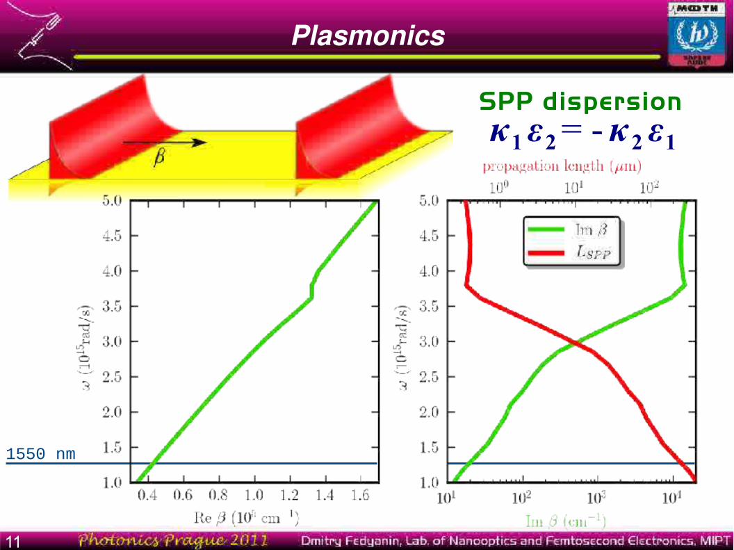
κ1 ε2 = - κ 2 ε1
SPP dispersion
-SPPwavevector
Lspp=1
2 Im k xpropagation length
spp=2
Re k xSPP wavelength
10
TM wave
Plasmonics
11
κ1 ε2 = - κ 2 ε1
SPP dispersion
D.Y. Fedyanin , A.V. Arsenin, Stored light in a plasmonic nanocavity based on extremelysmallenergyvelocity modes, Photon. Nanostruct.: Fundam. Appl., 8, 264272 (2010).
1550 nm

Plasmonics
12
κ1 ε2 = - κ 2 ε1
SPP dispersion
D.Y. Fedyanin , A.V. Arsenin, Stored light in a plasmonic nanocavity based on extremelysmallenergyvelocity modes, Photon. Nanostruct.: Fundam. Appl., 8, 264272 (2010).
1550 nm
λ = 1550 nmλSPP ≈ 1.5 μmLSPP
≈ 270 μmρAir
≈ 2.5 μmρAu
≈ 23 nm

Passive Plasmonic Waveguides
13
Dielectric Loaded SPP Waveguides (DLSPPWs)Why DLSPPWs?
- Are easily fabricated- Are easily coupled to other passive devices due to their planar structure- High confinement and endurable propagation losses
A. V. Krasavin, A. V. Zayats, Siliconbased plasmonic waveguides, Opt. Express 18, 11791 (2010)
Si
LSPP10 m at telecom wavelengths
Effective index method

Active Plasmonic Waveguide
● M. Nezhad, K. Tezt and Y. Fainman, Opt. Express 12, 40724079 (2004)
●J. Seidel, S. Grafström and L. Eng, Phys. Rev. Lett. 94, 177401 (2005).
●M. A. Noginov, et al., Opt. Express 16, 1385 (2008).
●M.Ambati, Sung Hyun Nam, E. UlinAvila, D.A. Genov, G. Bartal, and X. Zhang, Nano Lett. (2008)
●I. De Leon and P. Berini, Opt Express 17, 20191 (2009).
●P. M. Bolger, W. Dickson, A. V. Krasavin, L. Liebscher, S. G. Hickey, D. V. Skryabin, and A. V. Zayats, Opt. Lett. 35, 1197–1199 (2010).
●and many other papers14
High propagation losses due to Joule heating restrict the application of SPPs. Thus, one should increase the SPP propagation length, i.e. partially or fully compensate Joule losses. This can be done by using an active media placed near a metal surface. In recent years, a number of paper devoted to the SPP amplification have been published

15
Is it possible to design a COMPACT SPP waveguide with NEGLIGIBLY SMALL LOSSES?Requirements:- Compact pumping- Full loss compensation- Сompatibility with compact SPP waveguides- Single mode guiding
Active Plasmonic Waveguide
Recently, we have proposed a novel scheme of SPP amplification that is based on a minority carrier injection in a metal–semiconductor diode. This scheme uses a compact electrical pumping instead of a bulky optical one. Moreover, the proposed technique can be used to obtain surface plasmon lasing and design spasers, actually nanoscale coherent light sources.
We answer YES !
D.Yu. Fedyanin, A.V. Arsenin, Surface plasmon polariton amplification in metalsemiconductor structures, Opt. Express, Vol. 19, No. 13, pp. 1252412531 (2011)

SPP Amplification
16
D.Yu. Fedyanin, A.V. Arsenin, Surface plasmon polariton amplification in metalsemiconductor structures, Opt. Express 19, 1252412531 (2011)

17
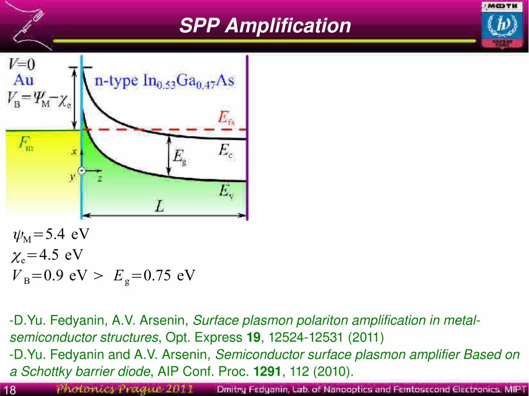
Usually, Schottky diodes are treated as majority carrier devices. However, the situation changes drastically when the metal work function ΨM exceeds χe+Eg/2, where
χe and Eg are the electron affinity
and the band gap of the semiconductor, respectively. In this case,an inversion layer is formed. Under forward bias, holes are injected into the bulk of the semiconductor and recombine with
electrons, that results in light emission. So, Schottky barriers can be used to design efficient and compact light- and plasmon-emitting diodes, but what about lasers and amplifiers? To design a laser, one should satisfy the condition for net stimulated emission or gain
K.W. Nill, A.R. Calawa, T. C. Harman and J.N. Walpole, Laser mission from metalsemiconductor barriers on PbTe and Pb0.8Sn0.2Te, Appl. Phys. Lett. 16, 375 (1970).D.Yu. Fedyanin and A.V. Arsenin, Semiconductor surface plasmon amplifier Based on a Schottky barrier diode, AIP Conf. Proc. 1291, 112 (2010).
F e−F hℏEg
SPP Amplification
18
D.Yu. Fedyanin, A.V. Arsenin, Surface plasmon polariton amplification in metalsemiconductor structures, Opt. Express 19, 1252412531 (2011)D.Yu. Fedyanin and A.V. Arsenin, Semiconductor surface plasmon amplifier Based on a Schottky barrier diode, AIP Conf. Proc. 1291, 112 (2010).
SPP Amplification
ψM=5.4 eVχe=4.5 eVV B=0.9 eV > E g=0.75 eV

19
SPP Amplification
We solve six nonlinear first order differential equations that describe the carrier behavior within the semiconductor
where
U=U stimU spontU Auger
D.Yu. Fedyanin, A.V. Arsenin, Surface plasmon polariton amplification in metalsemiconductor structures, Opt. Express 19, 1252412531 (2011)

20
SPP Amplification
together with six boundary conditions
where
nr≈14 8 k BT
mn
; pr≈14 8 k BT
mp
D.Yu. Fedyanin, A.V. Arsenin, Surface plasmon polariton amplification in metalsemiconductor structures, Opt. Express 19, 1252412531 (2011)

21
SPP Amplification
Stimulated emission and gain
L=400 nm, ΨM=5.4 eV,
εst=13.94, ε
opt=15.0,
χe=4.5 eV, E
g=0.75 eV that
correspond to Ga0.47
In0.53
As at T=300 K, donor concentration Nd=4.3x1018 cm-3, ħω=0.73 eV
(λ=1.7 μm).
g=4π 2e2
c n̄me02 ω
∣M b∣2∫
0
+∞
∣M env(E , E−ℏω)∣2
ρc(E−E c) ρv(E v−E+ℏω)×
{ 11+exp [(E−F e)/kBT ]
−
11+exp [(E−ℏω−F h)/kBT ] }dE
● Gaussian Halperin-Lax band-tail (GHLBT) model● Stern's envelope matrix element M
env
U stim( z)=g (F e( z) , F h( z)) S /ℏω

22
SPP Amplification
Stimulated emission and gain
L=400 nm, ΨM=5.4 eV,
εst=13.94, ε
opt=15.0,
χe=4.5 eV, E
g=0.75 eV that
correspond to Ga0.47
In0.53
As at T=300 K, donor concentration Nd=4.3x1018 cm-3, ħω=0.73 eV
(λ=1.7 μm).
g=4 π 2e2
c n̄me02 ω
∣M b∣2∫
0
+∞
∣M env(E , E−ℏω)∣2
ρc(E−E c) ρv(E v−E+ℏω)×
{ 11+exp [(E−F e)/kBT ]
−
11+exp [(E−ℏω−F h)/kBT ] }dE
≈8.76×10¹⁶(min (n , p)−3.7×10¹⁶)
U stim( z)=g (F e( z) , F h( z)) S / ℏω

23
Without gain: 2Imβ = 1630 cm-1
With gain: 2Imβ = -150 cm-1 (at V=1.07 V), so we have an amplification regime
SPP Amplification

24
Active Plasmonic Waveguide
What about of shrinking the lateral (y) dimension?There are no fundamental limitations for shrinking the lateral (y) dimension of the considered structure down to several hundred nanometers. Our structure has only two characteristic dimensions: thickness of the inversion layer and thickness of the depletion region. Both of them are appreciably less than 100 nm.
If the height h of the semiconductor region is large enough, we can consider only plasmonic modes at the metal-semiconductor interface and obtain a situation similar to DLSPPWs.

25
Active Plasmonic Waveguide
What about of shrinking the lateral (y) dimension?
εm=−141.6+15iεd=2.33εs=13.69
TM00
TM01
TM02

Summary
26
● Copper interconnects should be replaced by optical ones. However, despite the advantages of silicon photonics, even smaller interconnects are achievable with surface plasmon polariton based waveguides, which have the similar bandwidth and delays.● SPP waveguides are quite lossy. However, one can partially or fully compensate losses using an active medium placed near the metal surface. Compact electrical pumping can allow to use SPP waveguides in nanoscale circuits and design core-to-core and on-core interconnects.