Surface-Plasmon-Mediated Programmable Optical ... · XU ET AL. VOL. 8 ’ NO. 7 ’ 6682 – 6692...
11
XU ET AL. VOL. 8 ’ NO. 7 ’ 6682–6692 ’ 2014 www.acsnano.org 6682 June 04, 2014 C 2014 American Chemical Society Surface-Plasmon-Mediated Programmable Optical Nanofabrication of an Oriented Silver Nanoplate Bin-Bin Xu, † Lei Wang, † Zhuo-Chen Ma, † Ran Zhang, † Qi-Dai Chen, †, * Chao Lv, † Bing Han, † Xin-Ze Xiao, † Xu-Lin Zhang, † Yong-Lai Zhang, † Kosei Ueno, § Hiroaki Misawa, §, * and Hong-Bo Sun †,‡, * † State Key Laboratory on Integrated Optoelectronics, College of Electronic Science and Engineering, Jilin University, Changchun 130012, China, ‡ College of Physics, Jilin University, Changchun 130023, China, and § Research Institute for Electronic Science, Hokkaido University, Kita-Ku, Sapporo, Hokkaido 001-0021, Japan S ilver is considered particularly impor- tant due to its surface plasmon (SP) resonance wavelength at the visible spectral range and therefore is suitable for surface-enhanced Raman scattering (SERS) 15 and tip-enhanced Raman scattering (TERS), 6,7 photocatalysis, 8 and plasmonics. 9 Various nanofabrication technologies were adopted to produce silver nanostructures. Chemical approaches featuring bottom-up produc- tion of nanostructures, 10 including con- trolled reduction, seed-mediated growth, and template-directed growth, are advanta- geous in individual particle shape control and rapid production of a large amount of samples, but the capability of spatially ar- ranging nanostructures according to the requirements of device functions is appar- ently insufficient. In contrast, the nanofea- tures in top-down structures produced by, for example, electron beam lithography, focused ion beam lithography, and nano- sphere lithography are generally precisely designed, 1113 but the processing is re- strained by usage of photomasks, applica- tion solely to limited material species, and restrained geometries. Optical nanofabrica- tion has been demonstrated as an efficient technology in designing and achieving complex metal structures with nanometer accuracy either by pursuit of short-wave- length lasers down to extra ultraviolet to X-ray wavebands, 14 nonlinear lightmatter interactions including photon tunneling in near-field optics, 7,15,16 or multiphoton absorption in femtosecond laser direct writing. 1721 Especially in view of the fabri- cation precision, the designability of target structures, and the universality of useful materials, femtosecond laser direct writing is a relatively better choice, as proved by the enabled devices of microelectronical, 22 micro-optical, 23,24 micromechanical, 25 and microfluidic functions. 26,27 Femtosecond laser-induced photoreduc- tion of metal ions is an important optical method for fabricating nanostructures, by which three-dimensional (3D) nanowiring and 3D metal structures are realized. The laser-induced photochemical deposition of silver patterns is generally a nonlinear ab- sorption process; typically, when a single photon does not have enough energy to excite an electron from the valence to the conduction band, absorption of laser en- ergy can occur through a nonlinear process, * Address correspondence to [email protected], [email protected], [email protected]. Received for review December 26, 2013 and accepted June 4, 2014. Published online 10.1021/nn5029345 ABSTRACT We report polarized femtosecond laser-light- mediated growth and programmable assembly of photoreduced silver nanoparticles into triply hierarchical micropatterns. Formation of erected arrays of nanoplates with a thickness as small as λ/27 (λ, the writing laser wavelength) level is demonstrated. The growth mechanism of nanoplates has been clarified: (i) the excited surface plasmons enhance the local electric field and lead to spatially selective growth of silver atoms at the opposite ends of dipoles induced on early created silver seeds; (ii) the optical attractive force overcomes electrostatic repulsion in the enhanced local electric field to assemble the silver nanoparticles directly. The triply hierarchical micropattern shape and location, the nanoplate orientation, and thickness are all attained in controlled fashion. KEYWORDS: surface plasmons . silver . nanoplate . laser nanofabrication . SERS ARTICLE
-
Upload
trinhkhuong -
Category
Documents
-
view
216 -
download
0
Transcript of Surface-Plasmon-Mediated Programmable Optical ... · XU ET AL. VOL. 8 ’ NO. 7 ’ 6682 – 6692...

XU ET AL. VOL. 8 ’ NO. 7 ’ 6682–6692 ’ 2014
www.acsnano.org
6682
June 04, 2014
C 2014 American Chemical Society
Surface-Plasmon-MediatedProgrammable Optical Nanofabricationof an Oriented Silver NanoplateBin-Bin Xu,† Lei Wang,† Zhuo-Chen Ma,† Ran Zhang,† Qi-Dai Chen,†,* Chao Lv,† Bing Han,† Xin-Ze Xiao,†
Xu-Lin Zhang,† Yong-Lai Zhang,† Kosei Ueno,§ Hiroaki Misawa,§,* and Hong-Bo Sun†,‡,*
†State Key Laboratory on Integrated Optoelectronics, College of Electronic Science and Engineering, Jilin University, Changchun 130012, China, ‡College of Physics,Jilin University, Changchun 130023, China, and §Research Institute for Electronic Science, Hokkaido University, Kita-Ku, Sapporo, Hokkaido 001-0021, Japan
Silver is considered particularly impor-tant due to its surface plasmon (SP)resonance wavelength at the visible
spectral range and therefore is suitable forsurface-enhanced Raman scattering (SERS)1�5
and tip-enhanced Raman scattering (TERS),6,7
photocatalysis,8 and plasmonics.9 Variousnanofabrication technologies were adoptedto produce silver nanostructures. Chemicalapproaches featuring bottom-up produc-tion of nanostructures,10 including con-trolled reduction, seed-mediated growth,and template-directed growth, are advanta-geous in individual particle shape controland rapid production of a large amount ofsamples, but the capability of spatially ar-ranging nanostructures according to therequirements of device functions is appar-ently insufficient. In contrast, the nanofea-tures in top-down structures produced by,for example, electron beam lithography,focused ion beam lithography, and nano-sphere lithography are generally preciselydesigned,11�13 but the processing is re-strained by usage of photomasks, applica-tion solely to limited material species, andrestrained geometries. Optical nanofabrica-tion has been demonstrated as an efficient
technology in designing and achievingcomplex metal structures with nanometeraccuracy either by pursuit of short-wave-length lasers down to extra ultraviolet toX-ray wavebands,14 nonlinear light�matterinteractions including photon tunnelingin near-field optics,7,15,16 or multiphotonabsorption in femtosecond laser directwriting.17�21 Especially in view of the fabri-cation precision, the designability of targetstructures, and the universality of usefulmaterials, femtosecond laser direct writingis a relatively better choice, as proved bythe enabled devices of microelectronical,22
micro-optical,23,24 micromechanical,25 andmicrofluidic functions.26,27
Femtosecond laser-induced photoreduc-tion of metal ions is an important opticalmethod for fabricating nanostructures, bywhich three-dimensional (3D) nanowiringand 3D metal structures are realized. Thelaser-induced photochemical deposition ofsilver patterns is generally a nonlinear ab-sorption process; typically, when a singlephoton does not have enough energy toexcite an electron from the valence to theconduction band, absorption of laser en-ergy can occur through a nonlinear process,
* Address correspondence [email protected],[email protected],[email protected].
Received for review December 26, 2013and accepted June 4, 2014.
Published online10.1021/nn5029345
ABSTRACT We report polarized femtosecond laser-light-
mediated growth and programmable assembly of photoreduced
silver nanoparticles into triply hierarchical micropatterns. Formation
of erected arrays of nanoplates with a thickness as small as λ/27 (λ,
the writing laser wavelength) level is demonstrated. The growth
mechanism of nanoplates has been clarified: (i) the excited surface
plasmons enhance the local electric field and lead to spatially selective growth of silver atoms at the opposite ends of dipoles induced on early created silver
seeds; (ii) the optical attractive force overcomes electrostatic repulsion in the enhanced local electric field to assemble the silver nanoparticles directly. The
triply hierarchical micropattern shape and location, the nanoplate orientation, and thickness are all attained in controlled fashion.
KEYWORDS: surface plasmons . silver . nanoplate . laser nanofabrication . SERS
ARTIC
LE
XU ET AL. VOL. 8 ’ NO. 7 ’ 6682–6692 ’ 2014
www.acsnano.org
6683
which is known as multiphoton absorption.28 One ofthe most important issues for femtosecond laser-induced fabrication of metal structures is the realiza-tion of 3D structure and high resolution. For example,Kawata et al. reported fabrication of electrically con-ductive silver wires with a minimum width of 400 nmand 3D silver microstructures by using silver nitrateaqueous solution with coumarin 440 as a two-photonsensitive dye.29 Three-dimensional continuousmetallicstructures were fabricated by direct laser writing inpolymer composites containingmetal nanoparticles ormetal salts.26,27 A technology of flexible nanowiringof metal on nonplanar substrates by femtosecondlaser-induced electroless plating from metal ion pre-cursors was also demonstrated, by which a microhea-ter was integrated at the bed of the microfluidic chipchannel.22 These methods mainly depend on absorb-ing photons to provide energies to induce photore-duction and accelerate the reaction process occurringat limited microvolume of the laser focal spot. By now,through controlling the laser power according to thereaction threshold or inducing inhibitor molecules,the resolution could be increased beyond the opticaldiffraction limit. Although a resolution of 20 nm inphotopolymerization course through self-smoothingeffect was reported, the highest resolution obtained byTPA-induced fabrication of metal structures from anion precursor solution is about 100 nm.30
Conversion of light into surface plasmonwaves (SPs)leads to a significant wavelength reduction,31 consid-ered to be a promising avenue toward super-resolutionimaging,32 high-accuracy sensing,33,34 and on-chipoptical interconnection.35,36 The SPs based on noblemetals also play a crucial role in modification ofmolecular wave functions,37 photosensitization in can-cer therapy,38 and enhancement of solar cell powerconversion.39,40 Motion control of electrons by localfield-enhanced SPs fields built in semiconducting ormetallic nanostructures in terms of their shape, size,and periodicity of arrangement has been fully demon-strated.41�43 This scheme, however, has not beenutilized for optical nanofabrication but limited exam-ples of efforts in photochemical research; for example,Mirkin et al. introduced the concept of plasmonic seed-mediated triangular nanoprism shaping,44,45 and de-pending on the illumination wavelengths chosen, theplasmon excitations led either to fusion of nanoprismsin an edge-selective manner or to the growth of thenanoprisms until they reached a light-controlled finalsize. This method has been widely used to synthesizesilver nanoprisms and other related structures (e.g.,nanodisks or truncated prisms).46,47 Tatsuma et al.
reported the distribution of plasmon-induced chargeseparation sites at the Ag nanorod�TiO2 interface.
48,49
The charge separation sites are localized in almost thesame way as electric fields around the nanorods,indicating that the charge separation is induced or
promoted by the localized electric fields which facilitateapplication of the charge separation to nanofabricationandother nanolocalizedphotoelectrochemical reactions.48
Misawa et al. demonstrated for the first time that nano-particle plasmons can induce a detectable nanowire po-lymerization under irradiation by incoherent continuous-wave (CW) sources. Two-photon polymerization (TPP) ofthe photoresist surrounding the nanoparticles was foundin the high plasmonic field regions after irradiation by anincoherent light source, demonstrating that two-photonabsorption (TPA) triggered a photochemical reactionwith-out a laser source.50,51
Despite the broad studies on surface plasmonicsand the versatility of laser nanofabrication technolo-gies, SPs-induced local field enhancement has not yetbeen thought of as an effective means for assistingoptical fabrication of metal nanostructures. Herein,we report polarized femtosecond laser-light-mediatedgrowth and programmable assembly of photo-reduced silver nanoparticles into nanoplates andmicropatterns, during which the laser provides energy,optical force, and spatial resolution, which we call anoptical dynamic assembly process. The fabricatingsystem functions as an Otto configuration prism cou-pling system and was sufficient to excite SPs at theinterface between the metal and the lower-index pre-cursory solution.52 As far as we know, it is the firstreport of the formation of an erected array of nano-plates with a thickness of tens of nanometers as smallas λ/27 (λ, the writing laser wavelength) level, and it isattributed to spatially selective growth of silver atomsat the opposite ends of dipoles induced by highlylocalized and greatly enhanced electric fields on earlycreated silver seeds. The orientation of the nanoplateshas a strict dependence with the laser polarizationdirection.
RESULTS AND DISCUSSION
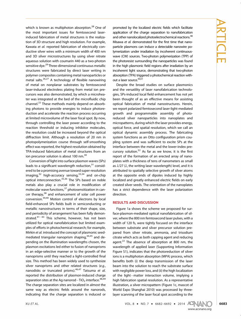
Figure 1a shows the scheme we proposed for sur-face-plasmon-mediated optical nanofabrication of sil-ver, where the 800 nm femtosecond laser pulses, with awidth of 120 fs, were tightly focused on the interfacebetween substrate and silver precursor solution pre-pared from silver nitrate, ammonia, and trisodiumcitrate which acts as both capping agent and reducingagent.22 The absence of absorption at 800 nm, thewavelength of applied laser (Supporting InformationFigure S1), indicates that the photoreduction of silverions is a multiphoton absorption (MPA) process, whichbenefits both (i) the deep transmission of the laserbeam into the solution to reach the substrate surfacewith negligible power loss, and (ii) the high localizationof the light�matter interaction volume, implying ahigh fabrication spatial resolution. As a representativeillustration, a silver micropattern (Figure 1c, mascot ofWorld Expo Shanghai 2010) was processed by three-layer scanning of the laser focal spot according to the
ARTIC
LE
XU ET AL. VOL. 8 ’ NO. 7 ’ 6682–6692 ’ 2014
www.acsnano.org
6684
designed program. In each layer of the writing, theplanar pattern program itself was kept identical but thelaser focal spot was vertically lifted for a distance,typically 50 nm. As a result of the unique 3D laserprocessing capability, the fabrication was not limitedto flat surfaces but possibly conducted in deep chan-nels (Figure 1a). For example, the silver sphere arraywith different diameters of 4.5, 8.5, and 12 μm werearranged at the intersections of two 30 μm deepmicrochannels (Figure 1b), which may serve as anintegrated SERS monitor in a microfluidic system tobe shown later. The capability of programmable as-sembly of the photoreduced nanoparticles is ensuredby the high-precision pinpoint laser writing scheme,which is not possibly fulfilled in various chemical self-organization processes. The patterns (Figure 1b,c) areconsidered as the first level of a triply hierarchicalstructure. As second level features, it is interesting torecognize from the magnified scanning electron mi-croscopic (SEM) image (Figure 1d) that the micropat-terns are actually composed of subwavelengthnanoplates. They are perpendicular to the substrateand possess a thickness on the order of several tens ofnanometers, which is one-tenth of the applied laserwavelength, and such small feature sizes have notbeen reported in laser-fabricated metal structures.The array of the erected nanoplates is apparently
different from the periodic structures created by inter-ference, either between the incident laser beams orbetween the incident beam and its excited waves,where patterns are replicas of light intensity
redistributions, and the structure periods depend inprinciple on the laser wavelength and the beamincident angles. Here, we attribute the nanoplate arrayproduction to local field enhancement induced by SPmode on silver particles. The initial silver nanoparticlesserving as seeds were produced in the first-layer laserscanning from the precursory solution through theMPA process, which is similar to the silver/gold micro-structures through a path of dot-by-dot and line-by-line reported before;18 in the course of second-layerlaser scanning, SP fields were significantly excited andestablished on the seeds, launching directional growthalong the dipole ends by attracting atoms that werephotoreducted in solution and the ripples and nano-plates were formed progressively (Figure 2c). Nano-particles are able to act as an electron storage andtransfer medium when the SPs are generated andthere is an increase of the chemical reactivity on itssurface.53,54 Hence, silver ions might more easily bereduced on the nanoparticle surface. In addition, forvery tinymetal nanoparticles, optical gradient force is amain part compared with scattering and absorptionforce.55,56 Under incident polarized light, the localelectric field of silver nanoparticles was enhanced,under which some other silver atoms or particles wereattracted due to optical gradient force along the dipoledirection to form longer and bigger nanostructures.They are developed from nanoparticles to ripples andfrom ripples to nanoplates. This essentially coincideswith what was reported by Tatsuma that plasmon-induced charge separation at the interface betweenAg
Figure 1. Surface-plasmon-mediated programmable optical nanofabrication of silver. (a) Scheme of femtosecond laser directwriting of silver triply hierarchical structures on a substrate. (b) SEM image of a Ag micropattern (the mascot of World ExpoShanghai 2010). (c) Locally magnified SEM image of themascot. (d) SEM image of a silver circle array patterned on the bed atthe intersection of two microchannels.
ARTIC
LE
XU ET AL. VOL. 8 ’ NO. 7 ’ 6682–6692 ’ 2014
www.acsnano.org
6685
nanorods and TiO2 was visualized by nanoscopic ima-ging of small satellite Ag nanoparticles deposited as aresult of the charge separation. The charge separationsites as well as localized electric fields around thenanorods are distributed anisotropically dependingon the excited plasmon modes, indicating that thecharge separation is localized and is induced or pro-moted by the localized electric fields.48,49
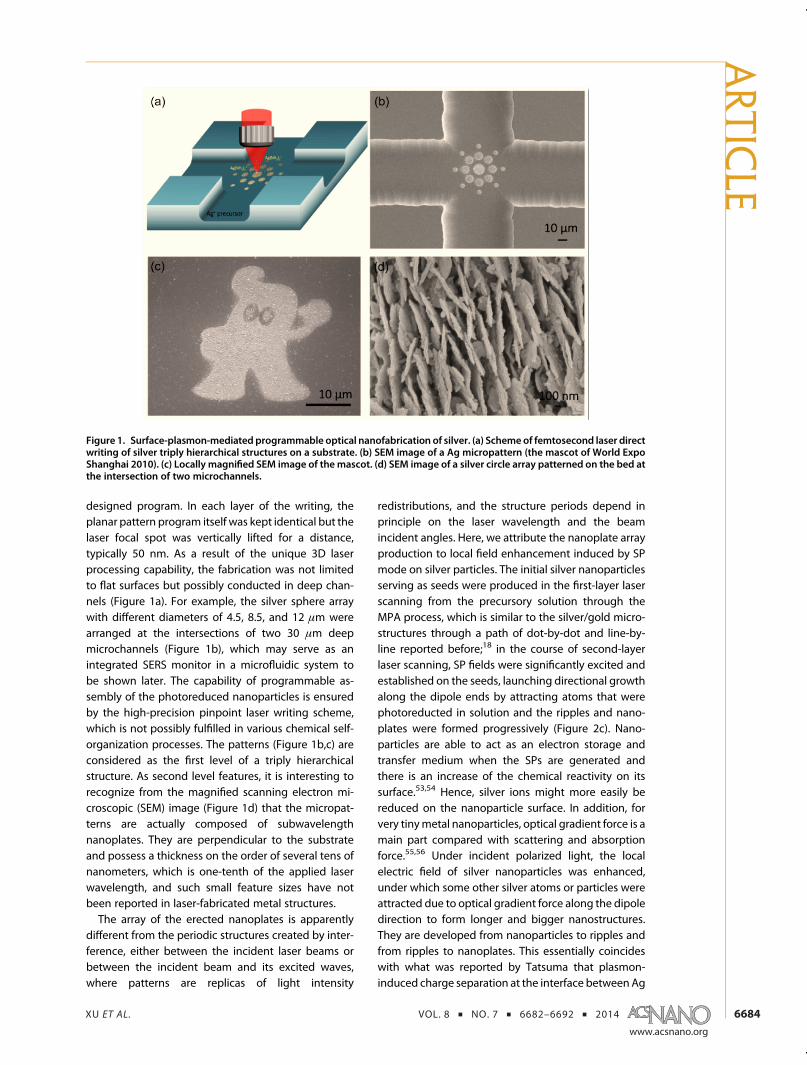
Figure 2 shows a simple estimation of the localelectric field distribution around a 50 nm silver nano-particle and a 300 nm silver ripple under excitation ofan 800 nm laser. The electric field intensity increaseswhen close to the surface of a silver nanoparticle/ripplewhich was demonstrated by the different colors inthe near region (Figure 2a,b). The optical gradientforce simulation is conducted to explain the processof the assembly of tiny clusters to form structures underthe focused laser field. During the first-layer scanningprocess, a continuous nanoparticle film was formedand the size of the nanoparticles distributed around50 nm, sowe just chose a single 50 nmnanosphere as asimulated sample to explain the ripple formationbased on nanoparticles in the second-layer scanningprocess in the next step. We suppose the simulatednanoparticle is relatively motionless and gave an en-hancement of local electric field, under which thesmaller clusters or ions were attracted to assemble inthe end. Similarly, we simulated that a ripple grewlonger to even form a nanoplate. We also attribute thisattraction force to optical gradient force and use thissimple model to show the assembly process directlyduring the formation of a single nanoplate. The opticalgradient force of attraction exerted by a 1 nm silver
nanoparticle by electric field near a pole of the dipolemay be as large as ∼pN, which is similar to a trappingforce of 2 pN/W/μm2 (numerical result) exerted on a50 nm diameter polystyrene bead in water that wasreported through an analytical Lorentz force model.57
The optical gradient force was shown as follows:F = 1/2RrE2, where E is the intensity of the electricfield and E2 the laser intensity, R is the polarizabilityof a nanoparticle; the detailed optical attracting forcemodel and calculation are given in the SupportingInformation. Obviously, the gradient force increaseswith the distance between the atoms with the surfaceof the dipoles along the fixed axis, as demonstrated bythe length of the red force arrows (Figure 2a,b).Although the single pulse duration is as short as100 fs, the relatively low scanning speed, around50 μm/s, and the finite focal spot size, ∼500 nm indiameter, estimated from the Airy spot size, leads to acontinuous crystal growth under irradiation for 1 ms,sufficient for diffusion of the surrounding ions andatoms (Figure 2c). Here, the incident ultrafast laserplays the roles of both photoreducing silver irons bymultiphoton absorption and, in themeantime, excitingSPs to direct the construction of nanostructures. Theinitial silver seed layer formation by laser scanningis critical, which guarantees appropriate surfaceroughness to ensure efficient coupling of light to SPmodes. Also, use of an oil-immersion high numericalaperture (NA, 1.40) objective lens is found to beindispensable for efficient SP coupling from the eva-nescent field built on a metal�solution interface,which constructs an Otto configuration prism couplingsystem (Figure S2).
Figure 2. (a) E-field distribution of a 50 nm silver seed and gradient force for attracting silver atoms in the dipole of the silverseed. (b) E-field distribution of 300 nm ripples andgradient force for attracting silver atoms in the dipole of the silver ripple. (c)Proposed mechanism for the formation of silver nanoplates.
ARTIC
LE
XU ET AL. VOL. 8 ’ NO. 7 ’ 6682–6692 ’ 2014
www.acsnano.org
6686
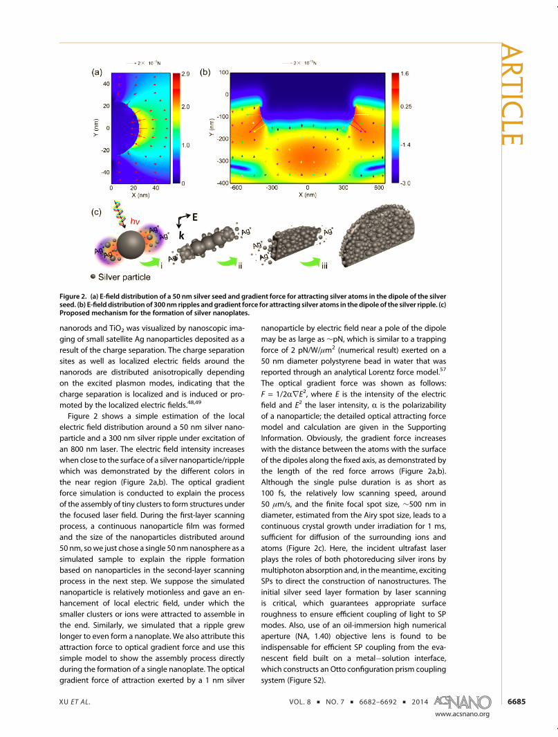
The above scenario was proved by the surfacefeature evolution in different stages of nanoplateformation in our experiments. The detailed multi-layer scanning process is shown as Figure S3. Duringthe first-layer scanning process, the silver nanoparti-cles were photoreduced, where some with sizes of20�80 nm were directly deposited on the surface ofsubstrate (glass) to form a film (Figure 3a) and otherssuspended in the vicinity. SPs could be excited in thesilver film that was sandwiched between a glass chipand precursor solution (insulator�metal�insulator,IMI). In the classical prism coupling scheme, SPs areconfined to the proximity of the metal�dielectricinterface and decay exponentially in both media. Thefabricating system functions as an Otto configurationprism coupling system, sufficient to excite SPs at theinterface between the metal and the lower-index pre-cursory solution. SPs can be excited, for example, by apolarized light incident onmetallic film from the side ofa glass prism at the critical angle θsp at which theprojection of the wave vector of the photon to thex axis, kx = k
√ε sin θsp is equal to ksp, is inherently leaky
waves which lose energy via absorption of the metal
and radiation into the lens (ε is the dielectric con-stant).58 In this case, the laser focusedbyanoil-immersionobjective lens propagates from optically dense medium(oil) to thinner medium (precursor solution�metal filminterface) which could achieve prism coupling of SPsusing attenuated total internal reflection.In the subsequent second-layer scanning process,
the ripples (Figure 3) were generated with subwave-length intervals of ∼200 nm, which is much smaller,considering that the wavelength of the femtosecondlaser is about 800 nm. To the best of our knowledge,the deep-subwavelength metal nanostructures pro-duced by photoreduction growth of metal ions havenot been reported. Resolution of 20 nmPt patterns wasachieved through photodeposition combined withmask assisting electron beam lithography.30 We deemthat these deep-subwavelength ripples were a syner-gistic effect by incident laser and excited SPs, which issimilar to some periodic subwavelength structuresmade by laser ablation on the solid substrate of aninsulator,59 semiconductor,60 or metals.61 The differ-ence is that the ripples they observed has a perpendi-cular relationship with the polarization of lasers.62
The transition/appearance (Figure 3c) and formation(Figure 3d) of plates were also shown as different stageoutcomes. According to the series of SEM images, thelengths ofmost of the nanoplates have values between1 and 2 μm. A scraped-off silver nanoplate is shown inFigure 3e, which is about 800 nm high and 2 μm long.In order to investigate the crystalline structure of thesesilver nanoplates, the sample was also characterizedby X-ray diffraction and high-resolution transmissionelectronmicroscopy (HR-TEM). The XRD spectra showedthe classic diffraction peak related to the lattice of the(111), (200), and (220) planes (Figure S4). These threepeaks were in accordance with the ones of Ag powder(Figure S5). The diffraction pattern of transmissionelectron microscopy (TEM) of the smooth bordershows that the nanoplate is a cubic-phase single crystal(Figure 3e). In the HR-TEM image (Figure 3e,f), thelattices of the [111] plane of cubic-phase silver couldbe easily identified, and the interplanar spacing ismeasured to be 0.24 nm, in agreement with thetheoretical value of 0.239 nm. Theoretical studiessuggest that citrate binds more strongly to Ag(111)than to Ag(100) surfaces at room temperature, whichfits well with these experimental results.63 Because ofthe stronger binding of citrate, the [111] facets areexpected to grow more slowly than the [100] facetswhen citrate ions are present. As a result, the [111]facets will become increasingly dominant on thesurface.43 In addition, some silver nanoparticles ad-hered to the surface of the nanoplate, and parts of thedetection area showed the polycrystalline structures ofthe silver nanoparticles. As shown in Figure S6, thelattice of the (111) and (200) planes could be clearlyidentified from the image, confirming their polycrystalline
Figure 3. SEM of different outcomes during the process offormation of nanoplates through tightly focused femtose-cond laser multilayer scanning process including differentsilver structures fabricated through tightly focused femto-second laser multilayer scanning process. (a) Silver filmcomposed of directed nanoseeds between 20 and 80 nmthrough single-layer scanning process. (b) Directed silverripples through bilayer scanning process. (c) Ripples trans-formed to nanoplates through triple-layer scanning pro-cess. (d) Upright nanoplates fabricated through four ormore than four-layer scanning process. (e) TEM image of asilver nanoplate; inset is the diffraction pattern. (f) HR-TEMimage of the edge of the nanoplate.
ARTIC
LE
XU ET AL. VOL. 8 ’ NO. 7 ’ 6682–6692 ’ 2014
www.acsnano.org
6687
properties. The interplanar spacings of these two planesare 0.24 and 0.20 nm, respectively, which are very close tothe theoretical values (0.236 and 0.201 nm). The inset ofFigure 2d is the electron diffraction pattern of the rougharea of this silver nanoplate, and the bright rings corre-spond to the (111), (200), (220), and (311) silver planes,confirming its polycrystalline structure.During the first-layer scanning process, photoche-
mical growth takes a leading role in controlling theshape and size of nanoparticle films that served asdipoles in the subsequent step; in the second, third,and more layer scanning steps, SPs begin to serve as amediator to induce the ripple and plate patterns. Thismodel is further evidenced by the polarization depen-dence experiment. The orientation of the plates wasnot found to be related to the scanning route in eitherthe mansard route or the involute coil route but wasdetermined by the polarization of the laser light. Asshown by SEM images of a series of 8 μm � 15 μmrectangles in Figure 4, nanoplates are always arrayedparallel to the laser polarization, as well as the electricfield direction of light and silver dipoles, which areindicated by inset arrows in Figure 4. Rotation of thepolarization of linear laser light causes sensitive corre-sponding change of the orientation of the upright
silver nanoplates. Figure 4a�d shows four differentdirections of nanoplate arrays, and the angle betweennanoplate orientation and horizontal direction chan-ged from 0� to 30, 60, and 90� when changing thedirection of laser polarization. It is consistent with theaxis characteristics of SPs induced by the enhancedlocal electric field. These results show the clear role ofSPs excitation in the nanoplates' growth.The concentration of silver precursor is also a vital
issue for processing. The UV�visible absorption spec-tra of different concentrations of silver precursor areshown in Figure 5. Obviously, the absorption peakswere all at 302 nm, and the intensity increases with theconcentration value accordingly. When the concentra-tion value was too low, for example, the absorptionpeak nearly disappeared at 0.00166 M. The differentconcentrations of silver precursor have differentlaser threshold power to induce photoreaction. Thesilver ion concentration we applied in this article is0.083 M, which we adopted as 0.02-, 0.1-, 0.5-, 5-, 10-,and 50-fold concentrations to study the threshold andmechanism. The threshold power and concentrationdependence is shown in Figure 5a. The lower concen-trations have higher threshold power. The thresholdvalue corresponding to 0.083Mwe used in the paper is0.8 mW, and the threshold nearly does not changewhen the concentration is greater than 0.083 M. Thesilver structures were different under different concen-trations. It is found that the nanoplates were difficult toproduce, and the structures were even discontinuousor some ripples appeared with lower concentrations,which was influenced by the poor ion supply anddelivery. When the concentration value is higher, thethickness of silver nanoplates increases, however, notso obviously compared with the change of the con-centration of silver ions and the nanoplates that seemto adhere to small particles more easily (Figure S7).At the same time, the silver precursor at high con-centration is easier to form a triangular nanoprismand truncated triangular nanoprism in solution. Thedeposited nanoparticles even go against the fabrica-tion when the concentration value attains 0.45 mol/L
Figure 4. Effect of laser beam polarization on the orienta-tion of silver nanoplates. (a�d) SEM images of silver hier-archical nanoplate array with different orientations byadjusting the laser polarization directions; the angles be-tween the polarization direction and horizontal directionwere 0, 30, 60, and 90�.
Figure 5. (a) Change of threshold power of photoreaction under different concentrations from 0.00166 to 4.15 M. (b)Nanoplates' thickness increasing with the laser power under a concentration of 0.083 M.
ARTIC
LE
XU ET AL. VOL. 8 ’ NO. 7 ’ 6682–6692 ’ 2014
www.acsnano.org
6688
(shown in Figure S8). This phenomenon coincides withthe series of work on the silver prisms reported byMirkin. The concentration of silver ions will influencethe material delivery and the photoreduction pro-cess directly. The order of magnitude analysis of heatand mass transport induced by Marangoni convectionwas given. The analysis suggests that the laser-inducedtemperature distribution develops within 1 ms andMarangoni convection flow commences within0.01�1 s, which increases by 1�2 orders of magnitudethe mass transfer of dissolved molecules into the laserfocus where they are trapped.64 The diffusion coeffi-cient of silver ions in water is 1.64� 10�9 m2/s, and thedelay for stabilization time for diffusion is ∼0.73�73 s.This suggests that the induced convection developedwithin∼1.2� 10�3 to 0.12 s can play a very significantrole. The extrapolated estimate shows that even in thecase of Mam = 4.18 � 103 (D = 1.64 � 10�9 m2/s) thisfactor reaches Deff/D ≈ 7; that is, a very strong en-hancement of mass transfer into the irradiated spottakes place. This means that during laser trapping theinduced Marangoni convection significantly increasesmass transfer within the area over which significantsurface tension gradients exist.With the SPs-mediated nanoplate directional
growth model confirmed, more phenomena could beinterpreted further. The larger laser intensity will pro-vide more energy for forming larger nanoparticlesas units which will construct thicker nanoplates. Wefabricated a silver hemisphere, and a 3D structure isshown in Figure S9 by a 50-layer scanning processunder different laser power. The thickness of thenanoplate increased with the applied laser power(Figure 5b). The values of the nanoplates' thicknessesare 29, 36, 45, 58, and 76 nm when applying a laserpower of 4, 5, 6, 7, and 9 mW, and the SEM images ofsome different thickness values of silver nanoplates areshown in Figure 6a�e. The attractive force generatedin the pole of the nanostructure is a mainly opticalgradient force in the enhanced optical field. The optical
gradient force will accelerate with the laser power, andthe assembly process of silver nanoparticles will also beenhanced. In addition, more photons will be providedunder higher laser power, which will accelerate thephotoreduction process of silver ions. Both of thesetwo impacts of enhanced assembly and photoreductionprocess will increase the thickness of silver nanoplates.The thinnest line width achieved by laser direct writingthrough the TPA process was about 100 nmas previouslyreported. In contrast, the thickness of the nanoplate herewas as small asλ/27 (λ, thewriting laserwavelength) level,far beyond the optical diffraction limit, and it is obviousthat SPs-mediated construction of metal structures couldbenefit from a lower limit line width and enhance thefabrication accuracy in optical nanofabrication. Throughthe lateral view of nanoplates (Figure 6f), we found thatthe surface of the nanoplates could still show a multiplestate, which confirms that the nanoplates were formeddue to the SPs-induced assembly of nanoparticles. So far,polarized femtosecond laser-induced photoreduction,growth, and programmable assembly of silver nanopar-ticles into nanoplates and micropatterns, during whichthe laser provides energy, excites SPs to assemble directlyand achieve high space resolution, so we call it an opticaldynamic assembly process.It was also found that the nanoplates could be
adhered with a series of nanoparticles, as shown inFigure 7. Statistical results show that the thicknessof the upright nanoplates in Figure 7a is in the rangeof 30�70 nm with an average value of ∼55 nm(Figure 7b). The diameter of the nanoparticles on thenanplates is between 25 and 80 nmwith a central valueof ∼50 nm (Figure 7c). These triply hierarchical nano-plates adhered with nanoparticles were providedas “hot spots” with an ultrahigh enhancement factorof 1011 with p-aminothiophenol (p-ATP) as the targetmolecule, with 514 nm laser as the excitation source(Figure 7d). The laser power of 10 mW combined withan elliptical spot size produced a power density of0.1 kW/cm�2. The typical accumulation time for each
Figure 6. (a�e) SEM images of the nanoplates with different thicknesses under different laser power. (f) Lateral view ofnanoplates in panel c.
ARTIC
LE

XU ET AL. VOL. 8 ’ NO. 7 ’ 6682–6692 ’ 2014
www.acsnano.org
6689
SERSmeasurement in this studywas 10 s. By simulatingan electric field of such adhered neighboring silvernanoparticles with the same diameter of 50 nm andwith a gap of 1 nm, the enhanced electromagnetic fieldE can reach a value of 800 (Figure S10). The reprodu-cible high enhancement factor should be associatedwith the fact that the SERS intensity is in directproportion to the fourth power of the field strength,|E|4. The 3D upright silver nanoplates will enhance theactual active surface, which is larger than the flatsurface under the same size of the laser spot. Theenhanced actual surface will benefit by absorbingmore molecules, so the collected signals were en-hanced relatively, which is also another advantagefor SERS detection. So the enhancement factor of1011 is based on both the enhanced actual absorbedsurface and the rough silver nanostructures just as thesilver island film. The rough surface of the nanoplateshould result from the fact that photogenerated atomsor small nanoparticles were attracted to the dipolesalong the dipole tips by optical gradient force in SP-enhanced electric field and also small particles ad-hered in the nanoplates through electrostatic force inthe vertical direction of the dipole ends; in other words,the thickness and smoothness of the nanoplates werealso influenced by electrostatic effect. The surfaces ofsilver nanoparticles were negatively charged becausethey were formed from silver ion solution with trisodiumcitrate acting as the capping agent. Citrate has threecarboxylic groups, and it has been shown by Munroet al.65 that mainly two of them would bind to the silversurface, leaving the third one normal to the surface andresponsible for the colloid stabilization by electrostaticrepulsion.44 So the SPs-induced directional assembly ofnanoparticles is a process of optical attraction force thatvanquishes electrostatic repulsion. In addition, the silver
Figure 7. Structural characterization of the hierar-chical silver substrate. (a) SEM image of the hierarchicalsilver substrate. (b) Thickness distribution of the nano-plates. (c) Size distribution of the nanoparticles. (d)SERS spectra of p-ATP molecules; the normalized inten-sity was gained by dividing the initial value by 10 mWand 10 s.
Figure 8. Thickness of silver nanoplates increases with the pH value of the precursor. (a) Photoreaction equation. (b)Nanoplate thickness increasing with the pH values. (c�f) SEM of different thickness of nanoplates with pH values of 10.8, 11,11.5, and 12.
ARTIC
LE
XU ET AL. VOL. 8 ’ NO. 7 ’ 6682–6692 ’ 2014
www.acsnano.org
6690
nanoparticle fusion is not efficient due to electrostaticrepulsion, which gives rise to the rough surface.The electrostatic force between nanoparticles de-
pends on the charge number that was affected by theionizing degree of capping agents when cappedwith acertain number of molecules. To clarify the electro-static force effect, we adjust the pH value of the silverprecursor with NaOH to study the changes of thenanoplates. We found that the thickness of nanoplatesincreasedwith the pH value from 10.8 to 12 (Figure 8b).However, the negative charges of the citrate anionincreasewith the pH of the solution. The increase of thenegative charges will increase the electrostatic forceand decrease the chance of nanoparticles adhering tothe side surface of the nanoplate freely, which willinfluence the roughness of the nanoplate. On the otherhand, the OH� is necessary in the photoreduction ofsilver ions,22,66 and the related reactionequation is shownin Figure 8a. The main OH� source comes from theionization of ammonia, and the photoreduction processwill be promoted when the pH value increases and thethickness of the nanoplates will increase, too. With pH 10as an example, the concentration of [OH�] is about10�4 M, and the precursor solution we used here is6.3 � 10�2 M; according to the reaction equation, the[OH�] is relatively insufficient. When the pH value is near12, the nanoplate is not only thicker but longer. Theoptical attractingmechanismwill competewith the staticrepulsion force under high pH value. However, the silverion precursor became muddy even with sediment, andthe high concentration of OH� resulted in the removal ofsilver ions from the precursor when the pH value ex-ceeded 12, which blocks the photoreaction.
CONCLUSION
In summary, a surface-plasmon-mediated programma-ble optical nanofabricationmethod was demonstrated
on silver. Three critical steps, namely, (i) seed produc-tion; (ii) excitation and coupling of light to localized SPsmodes and theirmediation to the directional growth ofnanoplates; and (iii) attraction of silver ions photore-ducted on the surface of nanoparticles and attractionof early produced nanoparticle assembly in the dipoleends. During these steps, the polarized laser pulsesprovide energy, excite SPs to assemble directly, andachieve high space resolution. The silver nanoplategrowth mechanism was clarified, and the SPs act as adirection guide for nanoplates growth, attract the silverions, and provide the driving force to overcome theelectrostatic repulsive force for nanoparticle assembly.The micropattern shape and location, the nanoplate
orientation, and the thickness are all attained incontrolled fashion. The triply hierarchical nanoplate(adheredwith nanoparticles)micropatternswere gaineddue to the inefficient fusion process between repulsivenanoparticles under high pH value. The laser powerthreshold decreases with the increase of the concentra-tion of silver precursor, and the Marangoni convectionsignificantly increases mass transfer within the area oflaser focus. The probability of free combination betweennanoparticles improved, and the thickness of the nano-plates increased from 60 to 300 nm when the pH valuewas changed from 10.8 to 12, during which the amountof OH� source is an important issue for photoreductionof silver ions. The thickness of the nanoplatewas as smallas λ/27 (λ, thewriting laserwavelength) level, far beyondthe optical diffraction limit, and it is obvious that SPs-mediated construction of metal structures could benefitfrom lower limit line width and enhance the fabricatingaccuracy in optical nanofabrication. In the future, SPs-assisted metal optical nanofabrication technology withtrue 3D and high precision structure fabrication onnanoelectronic devices and optical metamaterials mayfind broad application.
METHODS AND MATERIALS
Materials. Silver nitrate (AgNO3) and p-aminothiophenol(p-ATP) were purchased from Sigma-Aldrich Co., Ltd. Trisodiumcitrate (C6H5O6Na3), sodium hydroxide, and ammonia werepurchased from Beijing Chemicals Co., Ltd. The silver precursorwas prepared by dripping a suitable amount of aqueousammonia onto a mixture of silver nitrate aqueous solution(0.083 mol�1) and trisodium citrate (0.062 mol L�1) understirring until a clear solution was formed. The pH value of theprecursor was adjusted by adding NaOH solution. The micro-channel was fabricated on a normal glass substrate by usingphotolithography and wet etching techniques.
Femtosecond Laser Direct Writing Process. For each fabrication,the 800 nm femtosecond laser pulse, with a width of 120 fs andmode locked at 82 MHz (from Tsunami, Spectra Physics), wastightly focused by a high numerical aperture (NA = 1.4) oil-immersion objective lens (100�). The laser power was con-trolled by a gradual neutral density filter. The focal spot wasscanned laterally by steering a two galvano-mirror set and keptalong the optical axis by a piezo stage, both with high motionaccuracy. The silver nanoplates were fabricated with 1000 μs
exposure duration at each dot. All of the processes of fabricationwere controlled by a computer. The linear laser polarizationdirection was adjusted based on Glan prism and a half-waveplate.
Simulation. The optical electric field distribution of the nano-particle and nanorippple excited by an 800 nmwavelength lightwas simulated by the finite difference time domainmethod; theoptical gradient force distribution was gained throughMATLAB(Matrix Laboratory), and the gradient force was calculatedaccording to this formula:55
Fgrad ¼ jRj2rÆE2æ (1)
Characterization. The absorption spectra were measured on aShimadzu UV-3600 spectrometer. The surface morphologies ofthe samples weremeasured on a JEOL JSM-6700F field emissionscanning electron microscope operating at 3.0 keV. The crystal-line structure of the samples was characterized by a JEOL-2100FHR-TEM functioning at 200 kV. Surface-enhanced Raman spec-tra were measured on JOBIN YVON T64000 equipped with aliquid-nitrogen-cooled argon ion laser at 514.5 nm (Spectra-Physics
ARTIC
LE

XU ET AL. VOL. 8 ’ NO. 7 ’ 6682–6692 ’ 2014
www.acsnano.org
6691
Stabilite 2017) as excitation source (the laser power used wasabout 40 μWat the samples with an average spot size of 1 μm indiameter). The spectral resolution was 4 cm�1 at the excitationwavelength.
Conflict of Interest: The authors declare no competingfinancial interest.
Acknowledgment. The authors gratefully acknowledgesupport from 973 project (Grant Nos. 2011CB013003 and2013CBA01700), and National Science Foundation of China(NSFC) (Grant Nos. 51335008, 61378053, and 61377048). Thiswork is also supported by 2010 Ph.D. interdisciplinary projectNo. 450091102507, Jilin University.
Supporting Information Available: Absorption of silver pre-cursor, the highly focused laser beam exciting SPs, the layer-by-layer scanning process, the hierarchical silver nanoplate, theestimation of enhancement factor, and the enhanced electro-magnetic field E of the adhered nanoparticles. This material isavailable free of charge via the Internet at http://pubs.acs.org.
REFERENCES AND NOTES1. Cho, W. J.; Kim, Y.; Kim, J. K. Ultrahigh-Density Array of
Silver Nanoclusters for SERS Substrate with High Sensitivityand Excellent Reproducibility. ACS Nano 2011, 6, 249–255.
2. Zhu, Z.; Meng, H.; Liu, W.; Liu, X.; Gong, J.; Qiu, X.; Jiang, L.;Wang, D.; Tang, Z. Superstructures and SERS Properties ofGold Nanocrystals with Different Shapes. Angew. Chem.,Int. Ed. 2011, 50, 1593–1596.
3. Sun, M.; Zhang, Z.; Wang, P.; Li, Q.; Ma, F.; Xu, H. RemotelyExcited Raman Optical Activity Using Chiral PlasmonPropagation in AgNanowires. Light: Sci. Appl.2013, 2, e112.
4. Gervinskas, G.; Seniutinas, G.; Hartley, J. S.; Kandasamy, S.;Stoddart, P. R.; Fahim, N. F.; Juodkazis, S. Surface-EnhancedRaman Scattering Sensing on Black Silicon. Ann. Phys.2013, 525, 907–914.
5. Yokota, Y.; Ueno, K.; Juodkazis, S.; Mizeikis, V.; Murazawa,N.; Misawa, H.; Kasa, H.; Kintaka, K.; Nishii, J. Nano-texturedMetallic Surfaces for Optical Sensing and Detection Appli-cations. J. Photochem. Photobiol. A 2009, 207, 126–134.
6. Fleischer,M.;Weber-Bargioni, A.; Altoe,M. V. P.; Schwartzberg,A. M.; Schuck, P. J.; Cabrini, S.; Kern, D. P. Gold NanoconeNear-Field ScanningOptical Microscopy Probes. ACS Nano2011, 5, 2570–2579.
7. Kawata, S.; Inouye, Y.; Verma, P. Plasmonics for Near-FieldNano-imaging and Superlensing. Nat. Photonics 2009, 3,388–394.
8. Torimoto, T.; Horibe, H.; Kameyama, T.; Okazaki, K.-i.; Ikeda,S.; Matsumura, M.; Ishikawa, A.; Ishihara, H. Plasmon-Enhanced Photocatalytic Activity of Cadmium SulfideNanoparticle Immobilized on Silica-Coated Gold Particles.J. Phys. Chem. Lett. 2011, 2, 2057–2062.
9. Odom, T. W.; Schatz, G. C. Introduction to Plasmonics.Chem. Rev. 2011, 111, 3667–3668.
10. Stewart, M. E.; Anderton, C. R.; Thompson, L. B.; Maria, J.;Gray, S. K.; Rogers, J. A.; Nuzzo, R. G. NanostructuredPlasmonic Sensors. Chem. Rev. 2008, 108, 494–521.
11. De Angelis, F.; Gentile, F.; Mecarini, F.; Das, G.; Moretti, M.;Candeloro, P.; Coluccio, M. L.; Cojoc, G.; Accardo, A.;Liberale, C.; et al. Breaking the Diffusion Limit withSuper-hydrophobic Delivery of Molecules to PlasmonicNanofocusing SERS Structures. Nat. Photonics 2011, 5,682–687.
12. Ebbesen, T. W.; Lezec, H. J.; Ghaemi, H. F.; Thio, T.; Wolff,P. A. Extraordinary Optical Transmission through Sub-wavelength Hole Arrays. Nature 1998, 391, 667–669.
13. Masuda, H.; Fukuda, K. Ordered Metal Nanohole ArraysMade by a Two-Step Replication of Honeycomb Structuresof Anodic Alumina. Science 1995, 268, 1466–1468.
14. Grier, D. G. A Revolution in Optical Manipulation. Nature2003, 424, 810–816.
15. Fedoruk, M.; Lutich, A. A.; Feldmann, J. Subdiffraction-Limited Milling by an Optically Driven Single Gold Nano-particle. ACS Nano 2011, 5, 7377–7382.
16. Kumar, K.; Lee, K. K. C.; Li, J.; Nogami, J.; Kherani, N. P.;Herman, P. R. Quantized Structuring of Transparent Filmswith Femtosecond Laser Interference. Light: Sci. Appl.2014, 3, e157.
17. Shukla, S.; Vidal, X.; Furlani, E. P.; Swihart, M. T.; Kim, K.-T.;Yoon, Y.-K.; Urbas, A.; Prasad, P. N. Subwavelength DirectLaser Patterning of Conductive Gold Nanostructures bySimultaneous Photopolymerization and Photoreduction.ACS Nano 2011, 5, 1947–1957.
18. Zhang, Y.-L.; Chen, Q.-D.; Xia, H.; Sun, H.-B. Designable 3DNanofabrication by Femtosecond Laser Direct Writing.Nano Today 2010, 5, 435–448.
19. Kawata, S.; Sun, H.-B.; Tanaka, T.; Takada, K. Finer Featuresfor Functional Microdevices. Nature 2001, 412, 697–698.
20. Obata, K.; El-Tamer, A.; Koch, L.; Hinze, U.; Chichkov, B. N.High-Aspect 3D Two-Photon Polymerization StructuringwithWidenedObjectiveWorking Range (Wow-2pp). Light:Sci. Appl. 2013, 2, e116.
21. Sun, Y.-L.; Dong, W.-F.; Niu, L.-G.; Jiang, T.; Liu, D.-X.; Zhang,L.; Wang, Y.-S.; Chen, Q.-D.; Kim, D.-P.; Sun, H.-B. Protein-Based Soft Micro-optics Fabricated by Femtosecond LaserDirect Writing. Light: Sci. Appl. 2014, 3, e129.
22. Xu, B.-B.; Xia, H.; Niu, L.-G.; Zhang, Y.-L.; Sun, K.; Chen, Q.-D.;Xu, Y.; Lv, Z.-Q.; Li, Z.-H.; Misawa, H.; et al. Flexible Nanowiringof Metal on Nonplanar Substrates by Femtosecond-Laser-Induced Electroless Plating. Small 2010, 6, 1762–1766.
23. Wu, D.; Niu, L.-G.; Chen, Q.-D.; Wang, R.; Sun, H.-B. HighEfficiency Multilevel Phase-Type Fractal Zone Plates. Opt.Lett. 2008, 33, 2913–2915.
24. Juodkazis, S.; Mizeikis, V.; Misawa, H. Three-DimensionalMicrofabrication of Materials by Femtosecond Lasers forPhotonics Applications. J. Appl. Phys. 2009, 106, 051101.
25. Xia, H.; Wang, J.; Tian, Y.; Chen, Q.-D.; Du, X.-B.; Zhang, Y.-L.;He, Y.; Sun, H.-B. Ferrofluids for Fabrication of RemotelyControllable Micro-nanomachines by Two-Photon Poly-merization. Adv. Mater. 2010, 22, 3204–3207.
26. Wang, J.; He, Y.; Xia, H.; Niu, L.-G.; Zhang, R.; Chen, Q.-D.;Zhang, Y.-L.; Li, Y.-F.; Zeng, S.-J.; Qin, J.-H.; et al. Embellish-ment of Microfluidic Devices via Femtosecond LaserMicronanofabrication for Chip Functionalization. Lab Chip2010, 10, 1993–1996.
27. Sugioka, K.; Cheng, Y. Ultrafast Lasers;Reliable Tools forAdvanced Materials Processing. Light: Sci. Appl. 2014, 3,e149.
28. Malinauskas, M.; Farsari, M.; Piskarskas, A.; Juodkazis,S. Ultrafast Laser Nanostructuring of Photopolymers: ADecade of Advances. Phys. Rep. 2013, 533, 1–31.
29. Ishikawa, A.; Tanaka, T.; Kawata, S. Improvement in theReduction of Silver Ions in Aqueous Solution Using Two-Photon Sensitive Dye. Appl. Phys. Lett. 2006, 89, 113102.
30. Juodkazis, S.; Yamaguchi, A.; Ishii, H.; Matsuo, S.; Takagi, H.;Misawa, H. Photo-electrochemical Deposition of Platinumon TiO2 with Resolution of Twenty Nanometers Using aMask Elaborated with Electron-Beam Lithography. Jpn. J.Appl. Phys. 2001, 40, 4246.
31. Barnes, W. L.; Dereux, A.; Ebbesen, T. W. Surface PlasmonSubwavelength Optics. Nature 2003, 424, 824–830.
32. Hao, X.; Kuang, C.; Gu, Z.; Wang, Y.; Li, S.; Ku, Y.; Li, Y.; Ge, J.;Liu, X. From Microscopy to Nanoscopy via Visible Light.Light: Sci. Appl. 2013, 2, e108.
33. Dondapati, S. K.; Sau, T. K.; Hrelescu, C.; Klar, T. A.; Stefani,F. D.; Feldmann, J. Label-Free Biosensing Based on SingleGold Nanostars as Plasmonic Transducers. ACS Nano2010, 4, 6318–6322.
34. Ruach-Nir, I.; Bendikov, T. A.; Doron-Mor, I.; Barkay, Z.;Vaskevich, A.; Rubinstein, I. Silica-Stabilized Gold IslandFilms for Transmission Localized Surface Plasmon Sensing.J. Am. Chem. Soc. 2006, 129, 84–92.
35. Ahn, W.; Boriskina, S. V.; Hong, Y.; Reinhard, B. M. Photo-nic�Plasmonic Mode Coupling in On-Chip IntegratedOptoplasmonic Molecules. ACS Nano 2011, 6, 951–960.
36. Merlein, J.; Kahl, M.; Zuschlag, A.; Sell, A.; Halm, A.; Boneberg,J.; Leiderer, P.; Leitenstorfer, A.; Bratschitsch, R. Nanomecha-nical Control of an Optical Antenna. Nat. Photonics 2008, 2,230–233.
ARTIC
LE

XU ET AL. VOL. 8 ’ NO. 7 ’ 6682–6692 ’ 2014
www.acsnano.org
6692
37. Savasta, S.; Saija, R.; Ridolfo, A.; Di Stefano, O.; Denti, P.;Borghese, F. Nanopolaritons: Vacuum Rabi Splitting with aSingle Quantum Dot in the Center of a Dimer Nanoanten-na. ACS Nano 2010, 4, 6369–6376.
38. Wang, Y.; Chen, J.; Irudayaraj, J. Nuclear Targeting Dy-namics of Gold Nanoclusters for Enhanced Therapy ofHER2þ Breast Cancer. ACS Nano 2011, 5, 9718–9725.
39. Yang, J.; You, J.; Chen, C.-C.; Hsu, W.-C.; Tan, H.-R.; Zhang,X. W.; Hong, Z.; Yang, Y. Plasmonic Polymer Tandem SolarCell. ACS Nano 2011, 5, 6210–6217.
40. Choi, H.; Chen,W. T.; Kamat, P. V. Know ThyNanoNeighbor.Plasmonic versus Electron Charging Effects of Metal Nano-particles in Dye-Sensitized Solar Cells. ACS Nano 2012, 6,4418–4427.
41. Lee, S. Y.; Hung, L.; Lang, G. S.; Cornett, J. E.; Mayergoyz, I. D.;Rabin, O. Dispersion in the SERS Enhancement with SilverNanocube Dimers. ACS Nano 2010, 4, 5763–5772.
42. Schmucker, A. L.; Harris, N.; Banholzer, M. J.; Blaber, M. G.;Osberg, K. D.; Schatz, G. C.; Mirkin, C. A. CorrelatingNanorod Structure with Experimentally Measured andTheoretically Predicted Surface Plasmon Resonance. ACSNano 2010, 4, 5453–5463.
43. Rycenga, M.; Cobley, C. M.; Zeng, J.; Li, W.; Moran, C. H.;Zhang, Q.; Qin, D.; Xia, Y. Controlling the Synthesis andAssembly of Silver Nanostructures for Plasmonic Applica-tions. Chem. Rev. 2011, 111, 3669–3712.
44. Zhang, J.; Li, S.; Wu, J.; Schatz, G. C.; Mirkin, C. A. Plasmon-Mediated Synthesis of Silver Triangular Bipyramids. Angew.Chem., Int. Ed. 2009, 48, 7787–7791.
45. Jin, R.; Charles Cao, Y.; Hao, E.; Metraux, G. S.; Schatz, G. C.;Mirkin, C. A. Controlling Anisotropic Nanoparticle Growththrough Plasmon Excitation. Nature 2003, 425, 487–490.
46. Langille, M. R.; Zhang, J.; Mirkin, C. A. Plasmon-MediatedSynthesis of Heterometallic Nanorods and Icosahedra.Angew. Chem., Int. Ed. 2011, 50, 3543–3547.
47. Yoo, H.; Millstone, J. E.; Li, S.; Jang, J.-W.; Wei, W.; Wu, J.;Schatz, G. C.; Mirkin, C. A. Core�Shell Triangular Bifrus-tums. Nano Lett. 2009, 9, 3038–3041.
48. Kazuma, E.; Sakai, N.; Tatsuma, T. Nanoimaging of Loca-lized Plasmon-Induced Charge Separation. Chem. Com-mun. 2011, 47, 5777–5779.
49. Kazuma, E.; Matsubara, K.; Kelly, K. L.; Sakai, N.; Tatsuma, T.Bi- andUniaxiallyOrientedGrowth andPlasmonResonanceProperties of Anisotropic Ag Nanoparticles on SingleCrystalline TiO2 Surfaces. J. Phys. Chem. C 2009, 113,4758–4762.
50. Ueno, K.; Juodkazis, S.; Shibuya, T.; Yokota, Y.; Mizeikis, V.;Sasaki, K.; Misawa, H. Nanoparticle Plasmon-Assisted Two-Photon Polymerization Induced by Incoherent ExcitationSource. J. Am. Chem. Soc. 2008, 130, 6928–6929.
51. Geldhauser, T.; Ikegaya, S.; Kolloch, A.; Murazawa, N.; Ueno,K.; Boneberg, J.; Leiderer, P.; Scheer, E.; Misawa, H.Visualization of Near-Field Enhancements of Gold Trian-gles by Nonlinear Photopolymerization. Plasmonics 2011, 6,207–212.
52. Otto, A. Excitation of Nonradiative Surface Plasma Wavesin Silver by the Method of Frustrated Total Reflection. Z.Phys. 1968, 216, 398–410.
53. Henglein, A. Colloidal Silver Nanoparticles: PhotochemicalPreparation and Interaction with O2, CCl4, and SomeMetalIons. Chem. Mater. 1998, 10, 444–450.
54. Maillard, M.; Huang, P.; Brus, L. Silver Nanodisk Growth bySurface Plasmon Enhanced Photoreduction of Adsorbed[Agþ]. Nano Lett. 2003, 3, 1611–1615.
55. Xu, B.-B.; Zhang, R.; Wang, H.; Liu, X.-Q.; Wang, L.; Ma, Z.-C.;Chen, Q.-D.; Xiao, X.-Z.; Han, B.; Sun, H.-B. Laser Patterningof Conductive Gold Micronanostructures from Nanodots.Nanoscale 2012, 4, 6955–6958.
56. Svoboda, K.; Block, S. M. Optical Trapping of MetallicRayleigh Particles. Opt. Lett. 1994, 19, 930–932.
57. Seniutinas, G.; Rosa, L.; Gervinskas, G.; Brasselet, E.; Juodkazis,S. 3D Nano-structures for Laser Nano-manipulation. Beilstein.J. Nanotechnol. 2013, 4, 534–541.
58. Maier, S. A. Plasmonics: Fundamentals and Applications;Springer: New York, 2007.
59. Shimotsuma, Y.; Kazansky, P. G.; Qiu, J.; Hirao, K. Self-Organized Nanogratings in Glass Irradiated by UltrashortLight Pulses. Phys. Rev. Lett. 2003, 91, 247405.
60. Huang, M.; Zhao, F.; Cheng, Y.; Xu, N.; Xu, Z. Mechanisms ofUltrafast Laser-Induced Deep-Subwavelength Gratings onGraphite and Diamond. Phys. Rev. B 2009, 79, 125436.
61. Vorobyev, A. Y.; Makin, V. S.; Guo, C. Periodic Ordering ofRandom Surface Nanostructures Induced by FemtosecondLaser Pulses on Metals. J. Appl. Phys. 2007, 101, 034903.
62. Buividas, R.; Rosa, L.; �Sliupas, R.; Kudrius, T.; �Slekys, G.;Datsyuk, V.; Juodkazis, S. Mechanism of Fine Ripple For-mation on Surfaces of (Semi)Transparent Materials via aHalf-Wavelength Cavity Feedback. Nanotechnology 2011,22, 055304.
63. Kilin, D. S.; Prezhdo, O. V.; Xia, Y. Shape-Controlled Synthesisof Silver Nanoparticles: Ab Initio Study of Preferential Sur-face Coordination with Citric Acid. Chem. Phys. Lett. 2008,458, 113–116.
64. Louchev, O. A.; Juodkazis, S.; Murazawa, N.; Wada, S.;Misawa, H. Coupled Laser Molecular Trapping,ClusterAssembly, andDeposition FedbyLaser-InducedMarangoniConvection. Opt. Express 2008, 16, 5673–5680.
65. Munro, C. H.; Smith, W. E.; Garner, M.; Clarkson, J.; White,P. C. Characterization of the Surface of a Citrate-ReducedColloid Optimized for Use as a Substrate for Surface-Enhanced Resonance Raman Scattering. Langmuir 1995,11, 3712–3720.
66. Xue, C.; Métraux, G. S.; Millstone, J. E.; Mirkin, C. A. Mecha-nistic Study of Photomediated Triangular Silver NanoprismGrowth. J. Am. Chem. Soc. 2008, 130, 8337–8344.
ARTIC
LE