SUPREM-III User's Manual Version 8520 May 1985bariatto/fatec/spd/MAN_SUP6.pdf · Suprem-III User's...
96
SUPREM-III User's Manual Version 8520 May 1985 Stephen E. Hansen Copyright (C) May 7, 1985 by The Board of Trustees of Stanford University.
Transcript of SUPREM-III User's Manual Version 8520 May 1985bariatto/fatec/spd/MAN_SUP6.pdf · Suprem-III User's...
SUPREM-III User's Manual
Version 8520
May 1985
Stephen E. Hansen
Copyright (C) May 7, 1985
by The Board of Trustees of Stanford University.
Suprem-III User's Manual
2
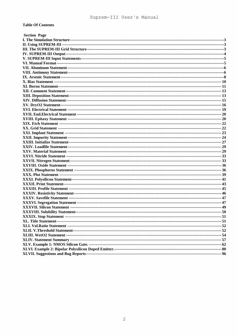
Table Of Contents
Section PageI. The Simulation Structure-------------------------------------------------------------------------------------------------------------------3II. Using SUPREM-III -------------------------------------------------------------------------------------------------------------------------3III. The SUPREM-III Grid Structure-------------------------------------------------------------------------------------------------------3IV. SUPREM-III Output ----------------------------------------------------------------------------------------------------------------------4V. SUPREM-III Input Statements-----------------------------------------------------------------------------------------------------------5VI. Manual Format -----------------------------------------------------------------------------------------------------------------------------5VII. Aluminum Statement ---------------------------------------------------------------------------------------------------------------------6VIII. Antimony Statement---------------------------------------------------------------------------------------------------------------------6IX. Arsenic Statement--------------------------------------------------------------------------------------------------------------------------8X. Bias Statement ----------------------------------------------------------------------------------------------------------------------------- 10XI. Boron Statement-------------------------------------------------------------------------------------------------------------------------- 11XII. Comment Statement -------------------------------------------------------------------------------------------------------------------- 13XIII. Deposition Statement------------------------------------------------------------------------------------------------------------------ 13XIV. Diffusion Statement-------------------------------------------------------------------------------------------------------------------- 15XV. DryO2 Statement------------------------------------------------------------------------------------------------------------------------ 16XVI. Electrical Statement ------------------------------------------------------------------------------------------------------------------- 19XVII. End.Electrical Statement ------------------------------------------------------------------------------------------------------------ 20XVIII. Epitaxy Statement ------------------------------------------------------------------------------------------------------------------- 20XIX. Etch Statement ------------------------------------------------------------------------------------------------------------------------- 22XX. Grid Statement -------------------------------------------------------------------------------------------------------------------------- 22XXI. Implant Statement --------------------------------------------------------------------------------------------------------------------- 23XXII. Impurity Statement------------------------------------------------------------------------------------------------------------------- 24XXIII. Initialize Statement ------------------------------------------------------------------------------------------------------------------ 27XXIV. Loadfile Statement------------------------------------------------------------------------------------------------------------------- 29XXV. Material Statement ------------------------------------------------------------------------------------------------------------------- 29XXVI. Nitride Statement -------------------------------------------------------------------------------------------------------------------- 33XXVII. Nitrogen Statement ----------------------------------------------------------------------------------------------------------------- 33XXVIII. Oxide Statement ------------------------------------------------------------------------------------------------------------------- 36XXIX. Phosphorus Statement -------------------------------------------------------------------------------------------------------------- 36XXX. Plot Statement ------------------------------------------------------------------------------------------------------------------------- 39XXXI. Polysilicon Statement---------------------------------------------------------------------------------------------------------------- 41XXXII. Print Statement---------------------------------------------------------------------------------------------------------------------- 43XXXIII. Profile Statement ------------------------------------------------------------------------------------------------------------------ 45XXXIV. Resistivity Statement -------------------------------------------------------------------------------------------------------------- 46XXXV. Savefile Statement ------------------------------------------------------------------------------------------------------------------ 47XXXVI. Segregation Statement ------------------------------------------------------------------------------------------------------------ 47XXXVII. Silicon Statement ----------------------------------------------------------------------------------------------------------------- 49XXXVIII. Solubility Statement------------------------------------------------------------------------------------------------------------- 50XXXIX. Stop Statement --------------------------------------------------------------------------------------------------------------------- 51XL. Title Statement--------------------------------------------------------------------------------------------------------------------------- 51XLI. Vol.Ratio Statement ------------------------------------------------------------------------------------------------------------------- 52XLII. V.Threshold Statement--------------------------------------------------------------------------------------------------------------- 52XLIII. WetO2 Statement -------------------------------------------------------------------------------------------------------------------- 54XLIV. Statement Summary ----------------------------------------------------------------------------------------------------------------- 57XLV. Example 1: NMOS Silicon Gate. --------------------------------------------------------------------------------------------------- 62XLVI. Example 2: Bipolar Polysilicon Doped Emitter.-------------------------------------------------------------------------------- 80XLVII. Suggestions and Bug Reports----------------------------------------------------------------------------------------------------- 96
Suprem-III User's Manual
3
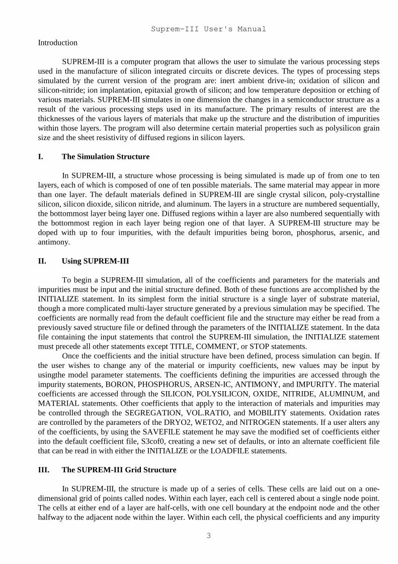
Introduction
SUPREM-III is a computer program that allows the user to simulate the various processing stepsused in the manufacture of silicon integrated circuits or discrete devices. The types of processing stepssimulated by the current version of the program are: inert ambient drive-in; oxidation of silicon andsilicon-nitride; ion implantation, epitaxial growth of silicon; and low temperature deposition or etching ofvarious materials. SUPREM-III simulates in one dimension the changes in a semiconductor structure as aresult of the various processing steps used in its manufacture. The primary results of interest are thethicknesses of the various layers of materials that make up the structure and the distribution of impuritieswithin those layers. The program will also determine certain material properties such as polysilicon grainsize and the sheet resistivity of diffused regions in silicon layers.
I. The Simulation Structure
In SUPREM-III, a structure whose processing is being simulated is made up of from one to tenlayers, each of which is composed of one of ten possible materials. The same material may appear in morethan one layer. The default materials defined in SUPREM-III are single crystal silicon, poly-crystallinesilicon, silicon dioxide, silicon nitride, and aluminum. The layers in a structure are numbered sequentially,the bottommost layer being layer one. Diffused regions within a layer are also numbered sequentially withthe bottommost region in each layer being region one of that layer. A SUPREM-III structure may bedoped with up to four impurities, with the default impurities being boron, phosphorus, arsenic, andantimony.
II. Using SUPREM-III
To begin a SUPREM-III simulation, all of the coefficients and parameters for the materials andimpurities must be input and the initial structure defined. Both of these functions are accomplished by theINITIALIZE statement. In its simplest form the initial structure is a single layer of substrate material,though a more complicated multi-layer structure generated by a previous simulation may be specified. Thecoefficients are normally read from the default coefficient file and the structure may either be read from apreviously saved structure file or defined through the parameters of the INITIALIZE statement. In the datafile containing the input statements that control the SUPREM-III simulation, the INITIALIZE statementmust precede all other statements except TITLE, COMMENT, or STOP statements.
Once the coefficients and the initial structure have been defined, process simulation can begin. Ifthe user wishes to change any of the material or impurity coefficients, new values may be input byusingthe model parameter statements. The coefficients defining the impurities are accessed through theimpurity statements, BORON, PHOSPHORUS, ARSEN-IC, ANTIMONY, and IMPURITY. The materialcoefficients are accessed through the SILICON, POLYSILICON, OXIDE, NITRIDE, ALUMINUM, andMATERIAL statements. Other coefficients that apply to the interaction of materials and impurities maybe controlled through the SEGREGATION, VOL.RATIO, and MOBILITY statements. Oxidation ratesare controlled by the parameters of the DRYO2, WETO2, and NITROGEN statements. If a user alters anyof the coefficients, by using the SAVEFILE statement he may save the modified set of coefficients eitherinto the default coefficient file, S3cof0, creating a new set of defaults, or into an alternate coefficient filethat can be read in with either the INITIALIZE or the LOADFILE statements.
III. The SUPREM-III Grid Structure
In SUPREM-III, the structure is made up of a series of cells. These cells are laid out on a one-dimensional grid of points called nodes. Within each layer, each cell is centered about a single node point.The cells at either end of a layer are half-cells, with one cell boundary at the endpoint node and the otherhalfway to the adjacent node within the layer. Within each cell, the physical coefficients and any impurity
Suprem-III User's Manual
4
concentrations are treated as constant. In the current version of the program there may be a maximum of500 node points or 499 cells or spaces. If an attempt is made to use more than the maximum number ofnode points during a simulation, the program will terminate with an error.
The distance between adjacent node points within each layer can be controlled by the user, eitherwhen a layer is first defined in an INITIALIZE or DEPOSITION statement or at any time in thesimulation through the GRID statement. The grid placement is controlled by five parameters; the layerthickness (THICKNESS), the nominal grid spacing (DX), the location of the nominal grid spacing relativeto the top surface of the layer (XDX), the number of spaces in the layer (SPACES), and the minimumallowed grid spacing (DX.MIN). The way these parameters are used to control the grid spacing isdescribed below. For the purposes of example, assume that a layer is being deposited on the structure.
In the simplest case the user need only specify the layer's thickness. In this case the program willassume that XDX is zero, placing the nominal grid spacing, DX, at the surface of the layer and will usethe default DX for the deposited material. The deposited material, specified by name, has itscharacteristics, including its default DX, defined by the appropriate material statement. The program willuse the number of spaces necessary to achieve a uniform grid spacing throughout the layer.
If the default DX is not adequate, then the user may specify both the thickness and the DX, and theprogram will work as above except that the specified DX will be used instead of the default value.
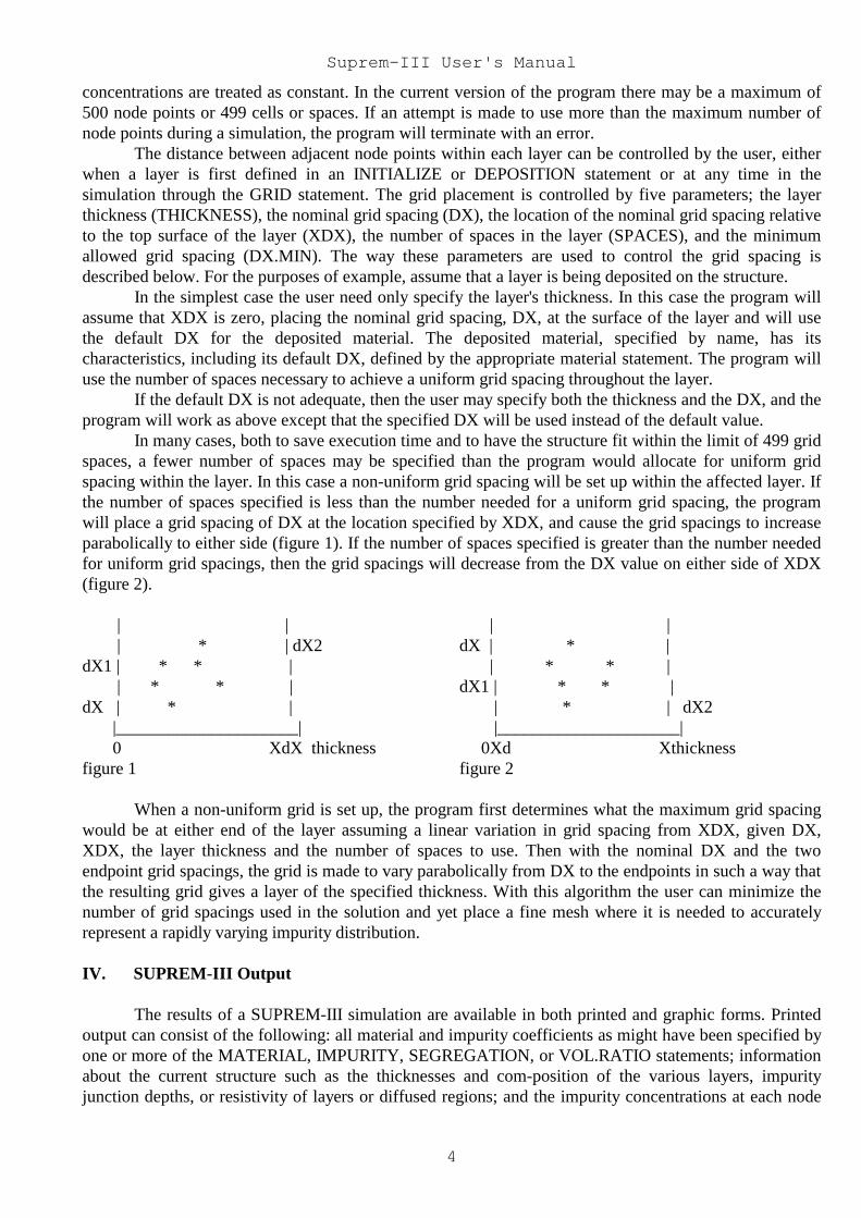
In many cases, both to save execution time and to have the structure fit within the limit of 499 gridspaces, a fewer number of spaces may be specified than the program would allocate for uniform gridspacing within the layer. In this case a non-uniform grid spacing will be set up within the affected layer. Ifthe number of spaces specified is less than the number needed for a uniform grid spacing, the programwill place a grid spacing of DX at the location specified by XDX, and cause the grid spacings to increaseparabolically to either side (figure 1). If the number of spaces specified is greater than the number neededfor uniform grid spacings, then the grid spacings will decrease from the DX value on either side of XDX(figure 2).
| | | * | dX2dX1 | * * | | * * |dX | * | |_____________________| 0 XdX thickness
| |dX | * | | * * |dX1 | * * | | * | dX2 |_____________________| 0Xd Xthickness
figure 1 figure 2
When a non-uniform grid is set up, the program first determines what the maximum grid spacingwould be at either end of the layer assuming a linear variation in grid spacing from XDX, given DX,XDX, the layer thickness and the number of spaces to use. Then with the nominal DX and the twoendpoint grid spacings, the grid is made to vary parabolically from DX to the endpoints in such a way thatthe resulting grid gives a layer of the specified thickness. With this algorithm the user can minimize thenumber of grid spacings used in the solution and yet place a fine mesh where it is needed to accuratelyrepresent a rapidly varying impurity distribution.
IV. SUPREM-III Output
The results of a SUPREM-III simulation are available in both printed and graphic forms. Printedoutput can consist of the following: all material and impurity coefficients as might have been specified byone or more of the MATERIAL, IMPURITY, SEGREGATION, or VOL.RATIO statements; informationabout the current structure such as the thicknesses and com-position of the various layers, impurityjunction depths, or resistivity of layers or diffused regions; and the impurity concentrations at each node
Suprem-III User's Manual
5
point and the distance of that point from the structure surface. Plotted or graphic output consists of plotsof the specified impurity concentrations versus distance.
V. SUPREM-III Input Statements
SUPREM-III normally takes its input from a user specified disk file. This file is madeup of variousstatements identified by a statement name followed by a parameter list. The statement name is delimitedfrom the parameter list by either a comma and/or one or more blanks. If a comma is present, it may bepreceded or followed by any number of blanks. Parameters in a SUPREM-III parameter list are delimitedfrom each other in the same way the statement name is delimited. If more than one line of input isrequired for a particular statement, it may be continued on subsequent lines by placing a plus sign as thefirst non-blank character on the continuation lines.
Parameters in a SUPREM-III parameter list may be one of three types that correspond to the typesof values that they may take on. These types are; Logical, numerical, and character. Logical parameterstake on a value of true if the parameter name appears by itself and a value of false if it is preceded by theNOT, (^), character. Numerical type parameters are assigned values in the parameter list by having theparameter name followed by an equal sign and the value. Blanks on either side of the equal sign areignored. Character parameters may appear in one of two ways depending of the statement involved. In onecase they have a formal parameter name and they are assigned a character string by use of an equal sign inthe same way as a numerical parameter. In the other case the statement has the character parameter as theonly valid parameter and the character string appears by itself following the statement name without anassociated parameter name.
VI. Manual Format
This manual presents each statement showing the statement name and the associated list ofparameters. There are a number of special characters that are used to aid in the description of theparameter lists. These characters are <, >, [, ], (, ), and |.
The <> characters are used to indicate classes of things. For example a parameter descriptionmight appear as: CONCENTRATION=<n>which indicates that the parameter name is concentration and it is assigned a numerical value. The <n>defines a class of things represented by n, where n represents the set of numerical values. Valid numericalvalues are of the form:9 1.2 -.345 6.7E8 -9.01E-2The only other class defined in this manual is that of character strings represented by <c>.
The [] characters enclose sets of optional items, usually parameters. For example:STMT1 [ PARM1 ] [ PARM2 PARM3 ] [ PARM4 [ PARM5 ] ]indicates that on the STMT1 statement, the PARM1 parameter is optional. PARM2 and PARM3 areoptional but if one is specified, both must be specified. PARM4 and PARM5 are optional but PARM5may be specified only if PARM4 is specified.
When one or more of a list of items are to be chosen from, they are separated by a | character andenclosed in parenthesis. For example:STMT2 (PARM1 | PARM2 | (PARM3 PARM4))This indicates that statement STMT2 requires that either PARM1, PARM2, or both PARM3 and PARM4be specified. In none of the above examples are the special characters actually typed by the user wheninputting a SUPREM-III input sequence.

Suprem-III User's Manual
6
VII. Aluminum Statement
The ALUMINUM statement is used to input or modify the characteristics of aluminum as a layermaterial.
ALUMINUM[ NAME=<c> ] [ DX.DEFAU=<n> ] [ CONDUCTO ] [ SPECIES=<n> ] [
DENSITY=<n> ][ AT.WT.1=<n> ] [ AT.NUM.1=<n> ] [ ABUND.1=<n> ] [ WORK.FUN=<n> ] [EPSILONF=<n> ]
Name Type Description Unit DefaultABUND.1 Num The relative abundance of element one
in the material. The sum of allabundances for a material must equalone.
the current value
AT.NUM.1 Num The atomic number of element one inthe material.
the current value
AT.WT.1 Num The atomic weight of element one inthe material.
amu the current value
CONDUCTO Log Specifies that the material is aconductor.
false
DENSITY Num The density of the material. grams/cm3 the current valueDX.DEFAU Num The default nominal grid spacing for
any layer containing this material.µm the current value
EPSILONF Num The dielectric constant of the materialrelative the dielectric constant of air.
the current value
NAME Char The name of the material. the current name of thematerial
SPECIES Num The number of different elements inthis material.
the current value
WORK.FUN Num The work function of the material. volts the current value
The ALUMINUM statement is an alias for the MATERIAL statement with an index of five and isused to define or modify the parameters and coefficients associated with the material aluminum. Not all ofthe parameters of the MATERIAL statement apply to aluminum and so are not listed here.
VIII. Antimony Statement
The ANTIMONY statement is used to input or modify the physical or model coefficientsassociated with antimony as a dopant impurity.
ANTIMONY[ NAME=<c> ] [ DONOR ] [ AT.WT=<n> ] [ AT.NUMB=<n> ] [ IONFILE1=<c> ] [
IONFILE2=<c> ][ ( ( SILICON [ FII.0=<n> ] [ FII.E=<n> ] [ K.MF=<n> ] [ K.A=<n> ] [ K.P=<n> ] ) | (
POLYSILI [ FII.0=<n> ] [ FII.E=<n> ] [ ENTROPY=<n> ] [ HEAT.SEG=<n> ] [ Q.SITES=<n> ]) | ( OXIDE | NITRIDE | ALUMINUM )
[ ELECT.ST=<n> ] [ DIX.0=<n> ] [ DIX.E=<n> ] [ DIM.0=<n> ] [ DIM.E=<n> ] [DIMM.0=<n> ] [ DIMM.E=<n> ] ]
Suprem-III User's Manual
7
Name Type Description Unit DefaultALUMINUM Log Specifies that the material dependent
parameters apply to antimony inaluminum
false
AT.NUMB Num The atomic number of the impurity the current valueAT.WT Num The atomic weight of the impurity amu the current valueDIM.0 Num The pre-exponential constant of the
diffusion coefficient of the impuritydiffusing with singly negative vacancies
µm 2/min. the current value
DIM.E Num The activation energy of the diffusioncoefficient of the impurity diffusing withsingly negative vacancies
eV the current value
DIMM.0 Num The pre-exponential constant of thediffusion coefficient of the impuritydiffusing with doubly negative vacancies
microns2/min. the current value
DIMM.E Num The activation energy of the diffusioncoefficient of the impurity diffusing withdoubly negative vacancies.
eV the current value
DIX.0 Num The pre-exponential constant of thediffusion coefficient of the impuritydiffusing with neutral vacancies.
µm 2/min. the current value
DIX.E Num The activation energy of the diffusioncoefficient of the impurity diffusing withneutral vacancies.
eV the current value
DONOR Log Specifies that the impurity is a donor. the current valueELECT.ST Num The electric stopping power of the
impurity in the specified material(KeV/ µm.) the current value
ENTROPY Num The entropy factor. Used to calculate theequilibrium segregation factor atpolysilicon grain boundaries.
the current value
FII.0 Num The pre-exponential constant of thefractional partial-interstitialcy contribution
(µm/min)-1/2 the current value
FII.E Num The activation energy of the fractionalpartial interstitialcy contribution
eV the current value
HEAT.SEG Num The activation energy of the equilibriumsegregation factor at polysilicon grainboundaries
eV the current value
IONFILE1 Char Specifies the primary ion implant rangedata file for implants using the analyticdistributions. This file will be searched forthe range statistics when implantingatomic antimony
the last filespecified
IONFILE2 Char Specifies the secondary ion implant rangedata file for implants using the analyticdistrbutions. This file will be searched forthe range statistics when implanting thecompound ions containing antimony.
the last filespecified
K.A Num Used in R. Reif's epitaxial doping model(see reference in EPITAXY statement).K.a is a thermodynamic constant relating
cm the current value
Suprem-III User's Manual
8
the dopant species concentration in solidsilicon and adsorbed layer
K.MF Num Used in R. Reif's epitaxial doping model(see reference in EPITAXY statement).K.mf is a kinetic coefficient controllingthe rate-limiting step of the dopantincorporation process
cm-2 min-1 atm-1 the current value
K.P Num Used in R. Reif's epitaxial doping model(see reference in EPITAXY statement).K.p is a thermodynamic constant relatingthe dopant species concentration in solidsilicon and gas phase
cm-3 atm-1 the current value
NAME Char The name of the impurity the last namespecified
NITRIDE Log Specifies that the material dependentparameters apply to antimony in siliconnitride
false
OXIDE Log Specifies that the material dependentparameters apply to antimony in silicondioxide
false.
POLYSILI Log Specifies that the material dependentparameters apply to antimony inpolysilicon
false
Q.SITES Num Effective density of segregation sites at agrain boundary
sites/cm2 the current value
SILICON Log Specifies that the material dependentparameters apply to antimony in silicon
false
The ANTIMONY statement is an alias for the IMPURITY statement with an index of four and isused to define or modify the parameters and coefficients associated with antimony as an impurity. Not allof the parameters of the IMPURITY statement apply to antimony and so are not listed here.
IX. Arsenic Statement
The ARSENIC statement is used to input or modify the physical or model coefficients associatedwith arsenic as a dopant impurity.
ARSENIC[ NAME=<c> ] [ DONOR ] [ AT.WT=<n> ] [ AT.NUMB=<n> ] [ IONFILE1=<c> ] [
IONFILE2=<c> ][ ( ( SILICON [ FII.0=<n> ] [ FII.E=<n> ] [ K.MF=<n> ] [ K.A=<n> ] [ K.P=<n> ] [ (
IMPLANT | CHEMICAL ) [ CTN.0=<n> ] [ CTN.E=<n> ] [ CTN.F=<n> ] ] ) | ( POLYSILI [ENTROPY=<n> ] [ HEAT.SEG=<n> ] [ Q.SITES=<n> ] [ FII.0=<n> ] [ FII.E=<n> ] [ (IMPLANT | CHEMICAL ) [ CTN.0=<n> ] [ CTN.E=<n> ] [ CTN.F=<n> ] ] ) | ( OXIDE |NITRIDE | ALUMINUM )
[ ELECT.ST=<n> ] [ DIX.0=<n> ] [ DIX.E=<n> ] [ DIM.0=<n> ] [ DIM.E=<n> ] [DIMM.0=<n> ] [ DIMM.E=<n> ] ]
Name Type Description Unit DefaultALUMINUM Log Specifies that the material dependent parameters
apply to arsenic in aluminum.false
Suprem-III User's Manual
9
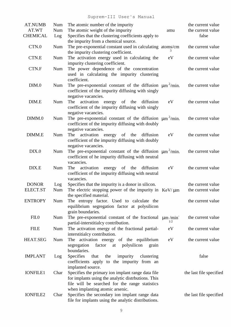
AT.NUMB Num The atomic number of the impurity the current valueAT.WT Num The atomic weight of the impurity amu the current value
CHEMICAL Log Specifies that the clustering coefficients apply tothe impurity from a chemical source.
false
CTN.0 Num The pre-exponential constant used in calculatingthe impurity clustering coefficient.
atoms/cm3
the current value
CTN.E Num The activation energy used in calculating theimpurity clustering coefficient.
eV the current value
CTN.F Num The power dependence of the concentrationused in calculating the impurity clusteringcoefficient.
the current value
DIM.0 Num The pre-exponential constant of the diffusioncoefficient of the impurity diffusing with singlynegative vacancies.
µm 2/min. the current value
DIM.E Num The activation energy of the diffusioncoefficient of the impurity diffusing with singlynegative vacancies.
eV the current value
DIMM.0 Num The pre-exponential constant of the diffusioncoefficient of the impurity diffusing with doublynegative vacancies.
µm 2/min. the current value
DIMM.E Num The activation energy of the diffusioncoefficient of the impurity diffusing with doublynegative vacancies.
eV the current value
DIX.0 Num The pre-exponential constant of the diffusioncoefficient of he impurity diffusing with neutralvacancies.
µm 2/min. the current value
DIX.E Num The activation energy of the diffusioncoefficient of the impurity diffusing with neutralvacancies.
eV the current value
DONOR Log Specifies that the impurity is a donor in silicon. the current valueELECT.ST Num The electric stopping power of the impurity in
the specified material.KeV/ µm the current value
ENTROPY Num The entropy factor. Used to calculate theequilibrium segregation factor at polysilicongrain boundaries.
the current value
FII.0 Num The pre-exponential constant of the fractionalpartial-interstitialcy contribution.
µm /min-
1/2the current value
FII.E Num The activation energy of the fractional partial-interstitialcy contribution.
eV the current value
HEAT.SEG Num The activation energy of the equilibriumsegregation factor at polysilicon grainboundaries.
eV the current value
IMPLANT Log Specifies that the impurity clusteringcoefficients apply to the impurity from animplanted source.
false
IONFILE1 Char Specifies the primary ion implant range data filefor implants using the analytic distrbutions. Thisfile will be searched for the range statisticswhen implanting atomic arsenic.
the last file specified
IONFILE2 Char Specifies the secondary ion implant range datafile for implants using the analytic distributions.
the last file specified

Suprem-III User's Manual
10
This file will be searched for the range statisticswhen implanting the compound ions containingarsenic.
K.A Num Used in R. Reif's epitaxial doping model (seereference in EPITAXY statement). K.a is athermodynamic constant relating the dopantspecies concentration in solid silicon andadsorbed layer.
cm the current value
K.MF Num Used in R. Reif's epitaxial doping model (seereference in EPITAXY statement). K.mf is akinetic coefficient controlling the rate-limitingstep of the dopant incorporation process.
cm-2
min.1 atm-
1
the current value
K.P Num Used in R. Reif's epitaxial doping model (seereference in EPITAXY statement). K.p is athermodynamic constant relating the dopantspecies concentration in solid silicon and gasphase.
cm-3 atm-1 the current value
NAME Char The name of the impurity. the last namespecified
NITRIDE Log Specifies that the material dependent parametersapply to arsenic in silicon nitride.
false
OXIDE Log Specifies that the material dependent parametersapply to arsenic in silicon dioxide.
false.
POLYSILI Log Specifies that the material dependent parametersapply to arsenic in polysilicon.
false
Q.SITES Num Effective density of segregation sites at a grainboundary.
sites/cm2 the current value
SILICON Log Specifies that the material dependent parametersapply to silicon.
false.
The ARSENIC statement is an alias for the IMPURITY statement with an index of three and isused to define or modify the parameters and coefficients associated with arsenic as an impurity. Not all ofthe parameters of the IMPURITY statement apply to arsenic and so are not listed here.
X. Bias Statement
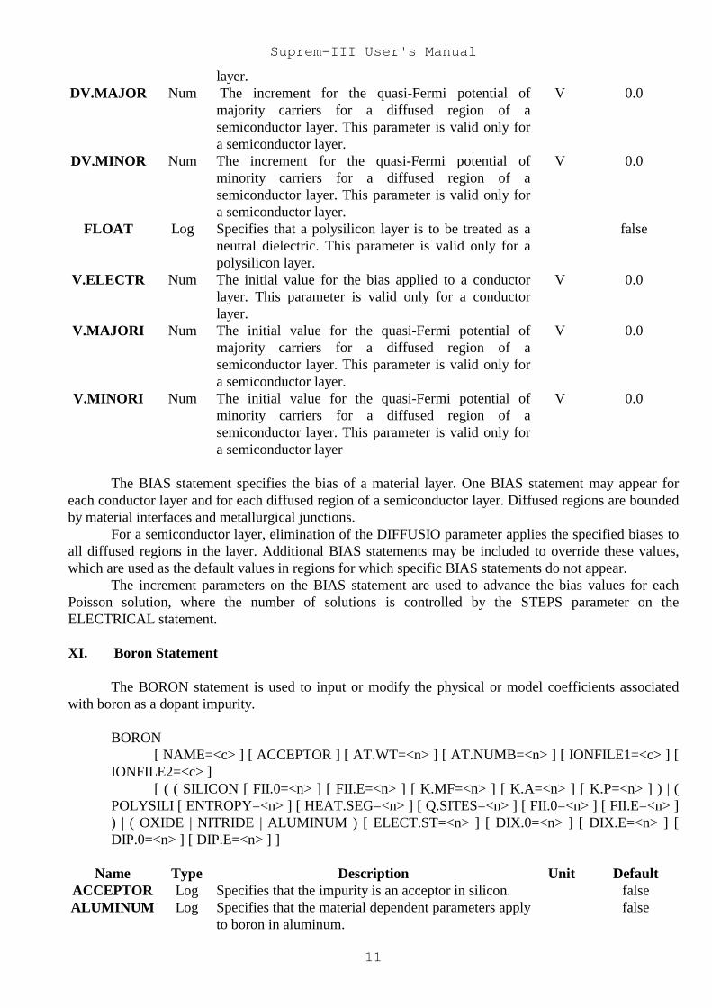
The BIAS statement is used to specify the bias of conductor and semiconductor layers during aPoisson solution initiated by the ELECTRICAL statement.
BIASLAYER=<n> ( [ V.ELECTR=<n> ] [ DV.ELECTR=<n> ] ) | ( ( [ DIFFUSIO=<n> ] [
V.MAJORI=<n> ] [ DV.MAJOR=<n> ] [ V.MINORI=<n> ] [ DV.MINOR=<n> ] ) | [ FLOAT ] )
Name Type Description Unit DefaultDIFFUSIO Num The index of the diffused region for which the quasi-
Fermi potentials are specified. The parameter is validonly for a semiconductor layer.
All diffusedregions in the
layerLAYER Num The index of the conductor or semiconductor layer
for which a bias is being specified.DV.ELECT Num The increment for the bias applied to a conductor
layer. This parameter is valid only for a conductorV 0.0
Suprem-III User's Manual
11
layer.DV.MAJOR Num The increment for the quasi-Fermi potential of
majority carriers for a diffused region of asemiconductor layer. This parameter is valid only fora semiconductor layer.
V 0.0
DV.MINOR Num The increment for the quasi-Fermi potential ofminority carriers for a diffused region of asemiconductor layer. This parameter is valid only fora semiconductor layer.
V 0.0
FLOAT Log Specifies that a polysilicon layer is to be treated as aneutral dielectric. This parameter is valid only for apolysilicon layer.
false
V.ELECTR Num The initial value for the bias applied to a conductorlayer. This parameter is valid only for a conductorlayer.
V 0.0
V.MAJORI Num The initial value for the quasi-Fermi potential ofmajority carriers for a diffused region of asemiconductor layer. This parameter is valid only fora semiconductor layer.
V 0.0
V.MINORI Num The initial value for the quasi-Fermi potential ofminority carriers for a diffused region of asemiconductor layer. This parameter is valid only fora semiconductor layer
V 0.0
The BIAS statement specifies the bias of a material layer. One BIAS statement may appear foreach conductor layer and for each diffused region of a semiconductor layer. Diffused regions are boundedby material interfaces and metallurgical junctions.
For a semiconductor layer, elimination of the DIFFUSIO parameter applies the specified biases toall diffused regions in the layer. Additional BIAS statements may be included to override these values,which are used as the default values in regions for which specific BIAS statements do not appear.
The increment parameters on the BIAS statement are used to advance the bias values for eachPoisson solution, where the number of solutions is controlled by the STEPS parameter on theELECTRICAL statement.
XI. Boron Statement
The BORON statement is used to input or modify the physical or model coefficients associatedwith boron as a dopant impurity.
BORON[ NAME=<c> ] [ ACCEPTOR ] [ AT.WT=<n> ] [ AT.NUMB=<n> ] [ IONFILE1=<c> ] [
IONFILE2=<c> ][ ( ( SILICON [ FII.0=<n> ] [ FII.E=<n> ] [ K.MF=<n> ] [ K.A=<n> ] [ K.P=<n> ] ) | (
POLYSILI [ ENTROPY=<n> ] [ HEAT.SEG=<n> ] [ Q.SITES=<n> ] [ FII.0=<n> ] [ FII.E=<n> ]) | ( OXIDE | NITRIDE | ALUMINUM ) [ ELECT.ST=<n> ] [ DIX.0=<n> ] [ DIX.E=<n> ] [DIP.0=<n> ] [ DIP.E=<n> ] ]
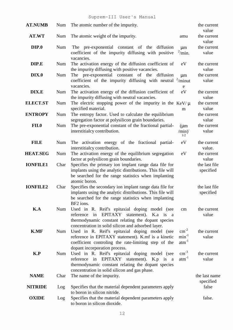
Name Type Description Unit DefaultACCEPTOR Log Specifies that the impurity is an acceptor in silicon. falseALUMINUM Log Specifies that the material dependent parameters apply
to boron in aluminum.false
Suprem-III User's Manual
12
AT.NUMB Num The atomic number of the impurity. the currentvalue
AT.WT Num The atomic weight of the impurity. amu the currentvalue
DIP.0 Num The pre-exponential constant of the diffusioncoefficient of the impurity diffusing with positivevacancies.
µm2/min.
the currentvalue
DIP.E Num The activation energy of the diffusion coefficient ofthe impurity diffusing with positive vacancies.
eV the currentvalue
DIX.0 Num The pre-exponential constant of the diffusioncoefficient of the impurity diffusing with neutralvacancies.
µm2/minut
e
the currentvalue
DIX.E Num The activation energy of the diffusion coefficient ofthe impurity diffusing with neutral vacancies.
eV the currentvalue
ELECT.ST Num The electric stopping power of the impurity in thespecified material.
KeV/ µm
the currentvalue
ENTROPY Num The entropy factor. Used to calculate the equilibriumsegregation factor at polysilicon grain boundaries.
the currentvalue
FII.0 Num The pre-exponential constant of the fractional partial-interstitialcy contribution.
(µm/min)-
1/2
the currentvalue
FII.E Num The activation energy of the fractional partial-interstitialcy contribution.
eV the currentvalue.
HEAT.SEG Num The activation energy of the equilibrium segregationfactor at polysilicon grain boundaries.
eV the currentvalue
IONFILE1 Char Specifies the primary ion implant range data file forimplants using the analytic distributions. This file willbe searched for the range statistics when implantingatomic boron.
the last filespecified
IONFILE2 Char Specifies the secondary ion implant range data file forimplants using the analytic distributions. This file willbe searched for the range statistics when implantingBF2 ions.
the last filespecified
K.A Num Used in R. Reif's epitaxial doping model (seereference in EPITAXY statement). K.a is athermodynamic constant relating the dopant speciesconcentration in solid silicon and adsorbed layer.
cm the currentvalue
K.MF Num Used in R. Reif's epitaxial doping model (seereference in EPITAXY statement). K.mf is a kineticcoefficient controling the rate-limiting step of thedopant incorporation process.
cm-2
min-1
atm-1
the currentvalue
K.P Num Used in R. Reif's epitaxial doping model (seereference in EPITAXY statement). K.p is athermodynamic constant relating the dopant speciesconcentration in solid silicon and gas phase.
cm-3
atm-1the current
value
NAME Char The name of the impurity. the last namespecified
NITRIDE Log Specifies that the material dependent parameters applyto boron in silicon nitride.
false
OXIDE Log Specifies that the material dependent parameters applyto boron in silicon dioxide.
false.
Suprem-III User's Manual
13
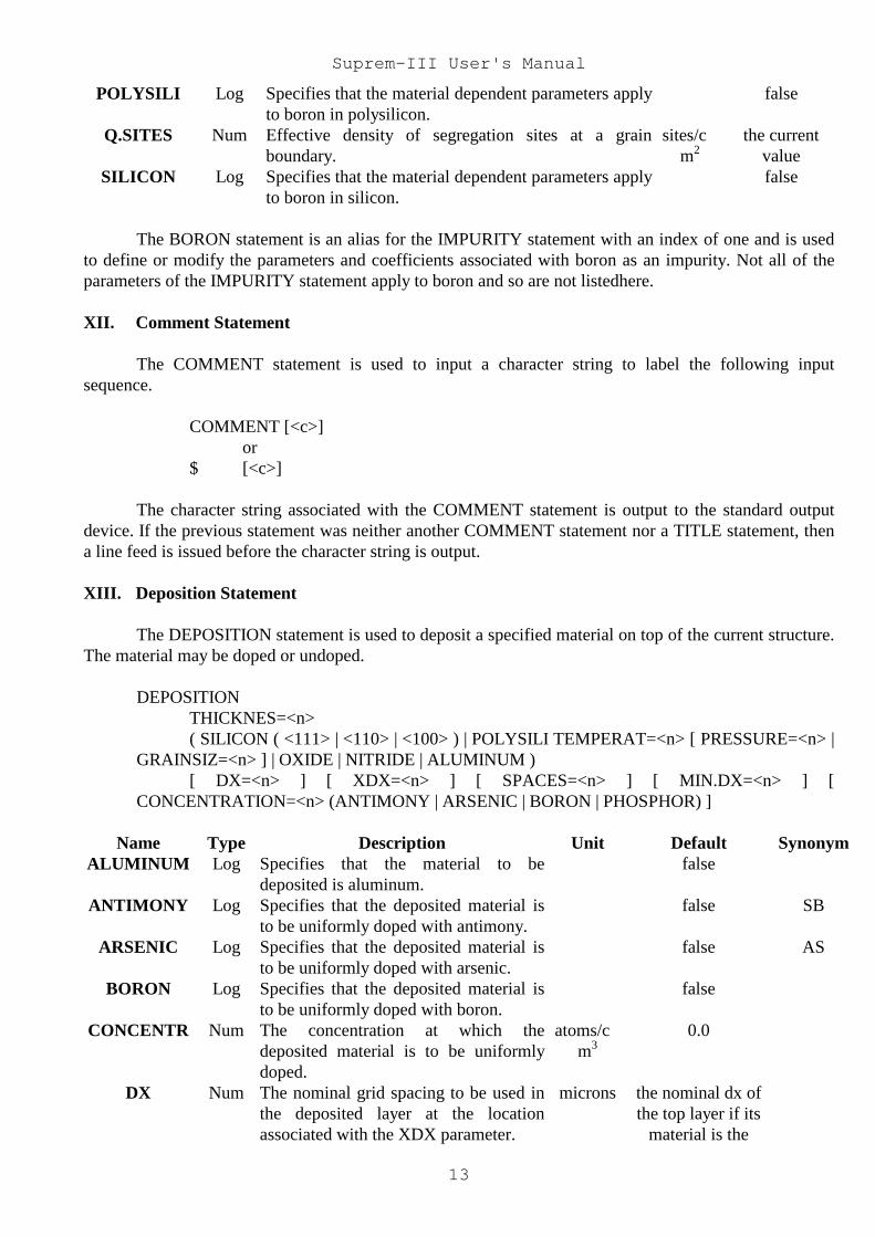
POLYSILI Log Specifies that the material dependent parameters applyto boron in polysilicon.
false
Q.SITES Num Effective density of segregation sites at a grainboundary.
sites/cm2
the currentvalue
SILICON Log Specifies that the material dependent parameters applyto boron in silicon.
false
The BORON statement is an alias for the IMPURITY statement with an index of one and is usedto define or modify the parameters and coefficients associated with boron as an impurity. Not all of theparameters of the IMPURITY statement apply to boron and so are not listedhere.
XII. Comment Statement
The COMMENT statement is used to input a character string to label the following inputsequence.
COMMENT [<c>]or
$ [<c>]
The character string associated with the COMMENT statement is output to the standard outputdevice. If the previous statement was neither another COMMENT statement nor a TITLE statement, thena line feed is issued before the character string is output.
XIII. Deposition Statement
The DEPOSITION statement is used to deposit a specified material on top of the current structure.The material may be doped or undoped.
DEPOSITIONTHICKNES=<n>( SILICON ( <111> | <110> | <100> ) | POLYSILI TEMPERAT=<n> [ PRESSURE=<n> |
GRAINSIZ=<n> ] | OXIDE | NITRIDE | ALUMINUM )[ DX=<n> ] [ XDX=<n> ] [ SPACES=<n> ] [ MIN.DX=<n> ] [
CONCENTRATION=<n> (ANTIMONY | ARSENIC | BORON | PHOSPHOR) ]
Name Type Description Unit Default SynonymALUMINUM Log Specifies that the material to be
deposited is aluminum.false
ANTIMONY Log Specifies that the deposited material isto be uniformly doped with antimony.
false SB
ARSENIC Log Specifies that the deposited material isto be uniformly doped with arsenic.
false AS
BORON Log Specifies that the deposited material isto be uniformly doped with boron.
false
CONCENTR Num The concentration at which thedeposited material is to be uniformlydoped.
atoms/cm3
0.0
DX Num The nominal grid spacing to be used inthe deposited layer at the locationassociated with the XDX parameter.
microns the nominal dx ofthe top layer if its
material is the
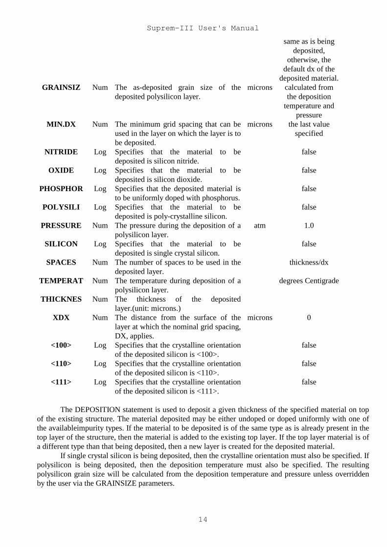
Suprem-III User's Manual
14
same as is beingdeposited,
otherwise, thedefault dx of the
deposited material.GRAINSIZ Num The as-deposited grain size of the
deposited polysilicon layer.microns calculated from
the depositiontemperature and
pressureMIN.DX Num The minimum grid spacing that can be
used in the layer on which the layer is tobe deposited.
microns the last valuespecified
NITRIDE Log Specifies that the material to bedeposited is silicon nitride.
false
OXIDE Log Specifies that the material to bedeposited is silicon dioxide.
false
PHOSPHOR Log Specifies that the deposited material isto be uniformly doped with phosphorus.
false
POLYSILI Log Specifies that the material to bedeposited is poly-crystalline silicon.
false
PRESSURE Num The pressure during the deposition of apolysilicon layer.
atm 1.0
SILICON Log Specifies that the material to bedeposited is single crystal silicon.
false
SPACES Num The number of spaces to be used in thedeposited layer.
thickness/dx
TEMPERAT Num The temperature during deposition of apolysilicon layer.
degrees Centigrade
THICKNES Num The thickness of the depositedlayer.(unit: microns.)
XDX Num The distance from the surface of thelayer at which the nominal grid spacing,DX, applies.
microns 0
<100> Log Specifies that the crystalline orientationof the deposited silicon is <100>.
false
<110> Log Specifies that the crystalline orientationof the deposited silicon is <110>.
false
<111> Log Specifies that the crystalline orientationof the deposited silicon is <111>.
false
The DEPOSITION statement is used to deposit a given thickness of the specified material on topof the existing structure. The material deposited may be either undoped or doped uniformly with one ofthe availableimpurity types. If the material to be deposited is of the same type as is already present in thetop layer of the structure, then the material is added to the existing top layer. If the top layer material is ofa different type than that being deposited, then a new layer is created for the deposited material.
If single crystal silicon is being deposited, then the crystalline orientation must also be specified. Ifpolysilicon is being deposited, then the deposition temperature must also be specified. The resultingpolysilicon grain size will be calculated from the deposition temperature and pressure unless overriddenby the user via the GRAINSIZE parameters.
Suprem-III User's Manual
15
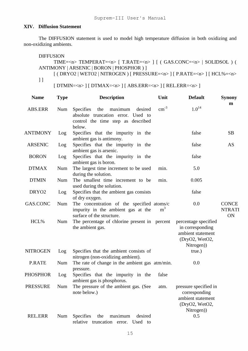
XIV. Diffusion Statement
The DIFFUSION statement is used to model high temperature diffusion in both oxidizing andnon-oxidizing ambients.
DIFFUSIONTIME=<n> TEMPERAT=<n> [ T.RATE=<n> ] [ ( GAS.CONC=<n> | SOLIDSOL ) (
ANTIMONY | ARSENIC | BORON | PHOSPHOR ) ][ ( DRYO2 | WETO2 | NITROGEN ) [ PRESSURE=<n> ] [ P.RATE=<n> ] [ HCL%=<n>
] ][ DTMIN=<n> ] [ DTMAX=<n> ] [ ABS.ERR=<n> ] [ REL.ERR=<n> ]
Name Type Description Unit Default Synonym
ABS.ERR Num Specifies the maximum desiredabsolute truncation error. Used tocontrol the time step as describedbelow.
cm-3 1.014
ANTIMONY Log Specifies that the impurity in theambient gas is antimony.
false SB
ARSENIC Log Specifies that the impurity in theambient gas is arsenic.
false AS
BORON Log Specifies that the impurity in theambient gas is boron.
false
DTMAX Num The largest time increment to be usedduring the solution.
min. 5.0
DTMIN Num The smallest time increment to beused during the solution.
min. 0.005
DRYO2 Log Specifies that the ambient gas consistsof dry oxygen.
false
GAS.CONC Num The concentration of the specifiedimpurity in the ambient gas at thesurface of the structure.
atoms/cm3
0.0 CONCENTRATI
ONHCL% Num The percentage of chlorine present in
the ambient gas.percent percentage specified
in correspondingambient statement(DryO2, WetO2,
Nitrogen))NITROGEN Log Specifies that the ambient consists of
nitrogen (non-oxidizing ambient).true.)
P.RATE Num The rate of change in the ambient gaspressure.
atm/min. 0.0
PHOSPHOR Log Specifies that the impurity in theambient gas is phosphorus.
false
PRESSURE Num The pressure of the ambient gas. (Seenote below.)
atm. pressure specified incorresponding
ambient statement(DryO2, WetO2,
Nitrogen))REL.ERR Num Specifies the maximum desired
relative truncation error. Used to0.5
Suprem-III User's Manual
16
control the time step as describedbelow.
SOLIDSOL Log Sets the concentration of the specifiedimpurity in the ambient gas at thesurface of the structure to the solidsolubility of the impurity in silicon.
false
TIME Num The total elapsed time of the diffusionstep being simulated.
min.
TEMPERAT Num The temperature of the ambient at thebeginning of the step.
°C
T.RATE Num The rate of change of the ambienttemperature.
°C /min. 0.0
WETO2 Log Specifies that the ambient gas consistsof wet oxygen or pyrogenic steam.(See note below.)
false
The DIFFUSION statement simulates impurity diffusion in the structure under a variety ofoxidizing and non-oxidizing conditions. At a minimum, only the time and temperature of a step needs tobe specified. In this case a non-oxidizing drive-in is assumed. For oxidizing ambients or gaseouspredepositions additional parameters need to be specified. The default pressures and chlorine percentagesare set previously by the oxidation ambient model cards (e.g. DRYO2, WETO2, NITROGEN),while thedefaults of the other optional parameters are set in the GENII key file S3FKY0.
The numerical solution of the diffusion equations requires that the total step time be divided into anumber of smaller time increments, dt's, in order to insure sufficient accuracy. There are two mechanismsthat control the choice of dt's, one is due to a restriction on interface movement such that no interfacemoves more than one cell spacing during a dt. The other time step control algorithm has been chosen togive the desired accuracy without using excessive amounts of computation time. Unless the interfacecontrol chooses a smaller dt, it will attempt to use a dt equal to that specified by the DTMIN parameter.Sub-sequent dt's are chosen in the following manner.
1. At each point in the current structure a projected concentration is calculated from the previoustwo solutions.
Cp = C' + (C' - C'')*dt/dt'Where C' is the previous concentration, C'' is the concentration before that, and dt' is the previous
dt.2. From the current solution value, C, and the absolute and relative truncation error parameters, an
`error' term at each point is then calculated.Cerr = abs(C - Cp) / (ABS.ERR + abs(C)*REL.ERR)
3. The next dt is then calculated from the following expression.dtnext = dt * sqrt( (1. + dt/dt')/Cerrmax )
Where Cerrmax is the maximum value of Cerr calculated at each point in the structure.4. A value of dtnext is calculated for each impurity present with the smallest value being the one
that is ultimately used.
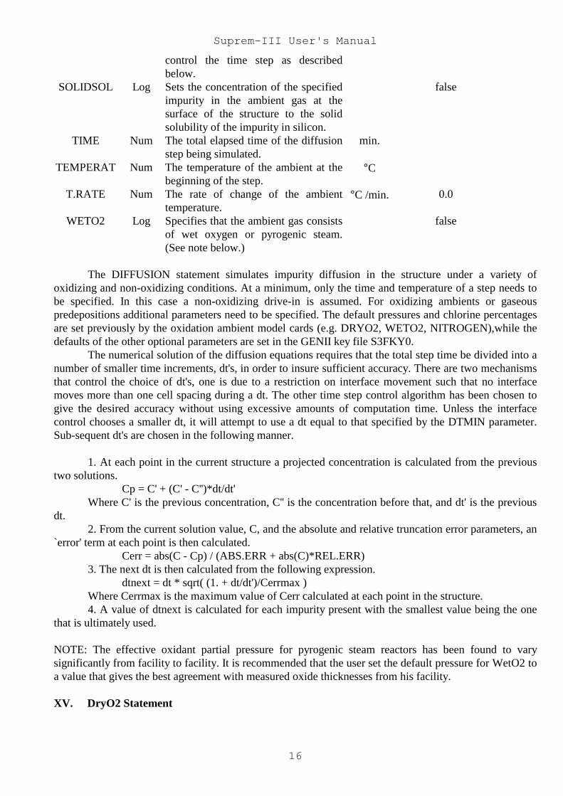
NOTE: The effective oxidant partial pressure for pyrogenic steam reactors has been found to varysignificantly from facility to facility. It is recommended that the user set the default pressure for WetO2 toa value that gives the best agreement with measured oxide thicknesses from his facility.
XV. DryO2 Statement
Suprem-III User's Manual
17
The DRYO2 statement allows the user to modify the coefficients used to model the oxidation ofthe various materials under dry ambient oxidation conditions.
DRYO2[ ( <111> | <110> | <100> ) [ LIN.L.0=<n> ] [ LIN.L.E=<n> ] [ LIN.H.0=<n> ] [
LIN.H.E=<n> ] [ THINOX.0=<n> ] [ THINOX.E=<n> ] [ THINOX.L=<n> ] ] [ PAR.L.0=<n> ] [PAR.L.E=<n> ] [ PAR.H.0=<n> ] [ PAR.H.E=<n> ] [ LIN.BREA=<n> ] [ PAR.BREA=<n> ] [LIN.PDEP=<n> ] [ PAR.PDEP=<n> ] [ PRESSURE=<n> ] [ HCL%=<n> ] [ GAMMA.0=<n> ] [GAMMA.E=<n> ] [ DELTA.0=<n> ] [ DELTA.E=<n> ] [ EXP.0=<n> ] [ EXP.E=<n> ] [ NIOX.0=<n> ][ NIOX.E=<n> ] [ NIOX.F=<n> ] [ CL.ROW=<n> [ CL.PCT=<n> ] CL.COLUM=<n> [CL.TEMPE=<n> ] [ CL.DEP.L=<n> ] [ CL.DEP.P=<n> ] ]
Name Type Description Unit DefaultCL.COLUM Num The column number in the table of coefficients used
to calculate the chlorine dependence of the oxidationrates.
the current value
CL.DEP.L Num The coefficient modifying the linear oxidation rate inthe presence of chlorine at the specified row andcolumn.
the current value
CL.DEP.P Num The coefficient modifying the parabolic oxidationrate in the presence of chlorine at the specified rowand column.
the current value
CL.PCT Num The percentage of chlorine for which the coefficientsin the specified row are valid.
percent the current value
CL.ROW Num The row number in the table of coefficients used tocalculate the chlorine dependence of the oxidationrates.
the current value
CL.TEMPE Num The temperature for which the coefficients in thespecified column are valid.
°C the current value
DELTA.0 Num The pre-exponential factor of the delta coefficientused in calculating the impurity concentrationdependence of the parabolic oxidation rate.
cm3/atom.
the current value
DELTA.E Num The activation energy of the delta coefficient used incalculating the impurity concentration dependence ofthe parabolic oxidation rate.
eV the current value
EXP.0 Num The pre-exponential factor of the exponent used incalculating the impurity concentration dependence ofthe parabolic oxidation rate.
the current value
EXP.E Num The activation energy of the exponent used incalculating the impurity concentration dependence ofthe parabolic oxidation rate.
eV the current value
GAMMA.0 Num The pre-exponential factor of the gamma coefficientused in calculating the impurity concentrationdependence of the linear oxidation rate.
the current value
GAMMA.E Num The activation energy of the gamma coefficient usedin calculating the impurity concentration dependenceof the linear oxidation rate.
eV the current value
HCL% Num The default percentage of chlorine present in theambient.
percent the current value
LIN.BREA Num The temperature at which the temperaturedependence of the linear oxidation rate changes.
°C the current value
Suprem-III User's Manual
18
LIN.H.0 Num The pre-exponential constant of the linear oxidationrate for temperatures above the breakpoint set byL.BREAKP.
microns/min.
the current value
LIN.H.E Num The activation energy of the linear oxidation rate fortemperatures above the breakpoint set byL.BREAKP.
eV the current value
LIN.L.0 Num The pre-exponential constant of the linear oxidationrate for temperatures below the breakpoint set byL.BREAKP.
microns/min.
the current value
LIN.L.E Num The activation energy of the linear oxidation rate fortemperatures below the breakpoint set byL.BREAKP.
eV the current value
LIN.PDEP Num The pressure dependence factor for the linearoxidation rate.
the current value
NIOX.0 Num The pre-exponential constant used to determine theoxidation rate of silicon nitride.
microns.
the current value
NIOX.E Num The activation energy used to determine theoxidation rate of silicon nitride.
eV the current value
NIOX.F Num The exponent factor used to determine the oxidationrate of silicon nitride.
the current value
PAR.BREA Num The temperature at which the temperaturedependence of the parabolic oxidation rate changes.
°C the current value
PAR.H.0 Num The pre-exponential constant of the parabolicoxidation rate for temperatures above the breakpointset by P.BREAKP.
microns2/min.
the current value
PAR.H.E Num The activation energy of the parabolic oxidation ratefor temperatures above the breakpoint set byP.BREAKP.
eV the current value
PAR.L.0 Num The pre-exponential constant of the parabolicoxidation rate for temperatures below the breakpointset by P.BREAKP.
microns2/min.
the current value
PAR.L.E Num The activation energy of the parabolic oxidation ratefor temperatures below the breakpoint set byP.BREAKP.
eV the current value.
PAR.PDEP Num The pressure dependence factor for the parabolicoxidation rate.
the current value
PRESSURE Num The default ambient pressure. atm. the current valueTHINOX.0 Num The pre-exponential constant of the thin oxide
growth rate parameter.microns/min.
the current value
THINOX.E Num The activation energy of the thin oxide growth rateparameter.
eV the current value
THINOX.L Num The characteristic length of the thin oxide growthrate parameter.
microns
the current value
<100> Log Specifies that the linear growth rate and thin oxidegrowth rate parameters apply to <100> orientationsilicon.
false
<110> Log Specifies that the linear growth rate and thin oxidegrowth rate parameters apply to <110> orientationsilicon.
false.
<111> Log Specifies that the linear growth rate and thin oxidegrowth rate parameters apply to <111> orientation
false
Suprem-III User's Manual
19
silicon.
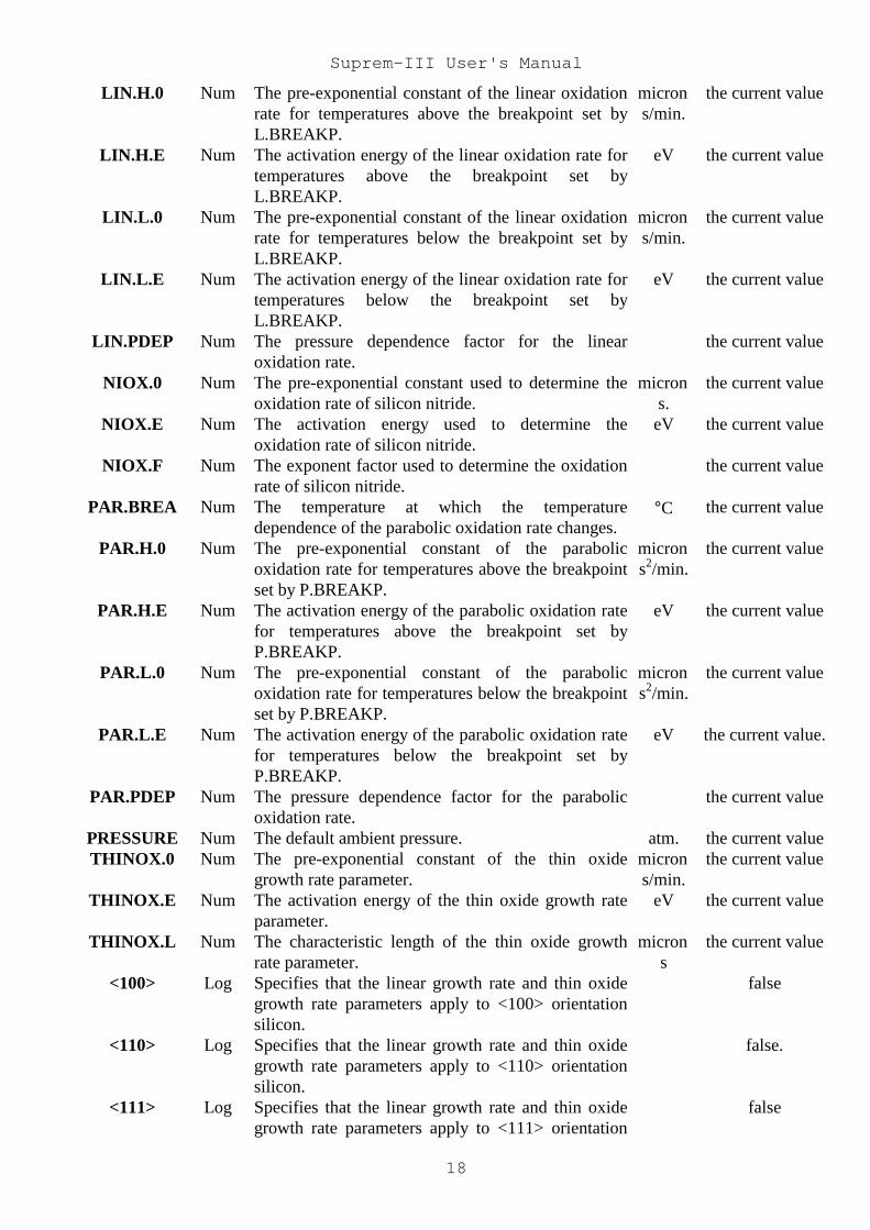
The three oxidation model statements, DRYO2, WETO2, and NITROGEN, use identicalparameters, differing only in the values assigned. The parameters NIOX.C, NIOX.E, and NIOX.F are usedin modeling the oxidation of silicon nitride while the others deal with the oxidation of single andpolycrystalline silicon.
The effects of chlorine in the ambient gas on the oxidation rate of silicon are currently modeled byan empirical expression whose only variable is defined by the L.CLDEP and P.CLDEP for the linear andparabolic rates respectively. To date no convenient function is available to calculate the chlorinedependence as a function of temperature and amount of chlorine present, therefor a table of values definesthe chlorine dependence factors at those temperatures and percentages for which reliable data is available.For those temperatures and chlorine percentages between the values in the table, linear interpolation isemployed to calculate the value used. For temperatures or percentages outside the range of values presentin the table, the values whose conditions most nearly match the current conditions are used. For example,if the current conditions are a temperature of 1175 degrees with three percent chlorine, but the highesttemperature entry in the table is 1150 degrees and the nearest chlorine percentages are for two and fourpercent, then a value halfway between the values at 1150 degrees and two and four percent chlorine willbe used.
XVI. Electrical Statement
The ELECTRICAL statement begins a series of numerical solutions of Poisson's equation for thecurrent structure.
ELECTRICAL[ STEPS=<n> ] [ EXTENT=<n> ] [ TEMPERAT=<n> ] [ ERROR=<n> ] [
MAX.ITER=<n> ] [ FILE.OUT=<c> ]
Name Type Description Unit DefaultERROR Num The allowed relative error between successive
approximations during the iterative solution of Poisson'sequation.
1 x 10⁻⁴
EXTENT Num The distance by which the bottom layer of the structure isextended for the numerical solution of Poisson's equation.This extension is necessary to allow for the proper treatmentof depletion regions which extend beyond the bottom of thesimulated structure.
microns 0.0
FILE.OUT char The name of the file to which the results of the electricalcalculations are to be output. The total hole and electronconcentrations and their respective conductivities andresistivities are normally written to the standard output, but ifa file is specified, they are also written to that file. Thepotential, net active impurity concentration and the distancefrom the surface at each node are also written to the file.
MAX.ITER Num The maximum number of iterations allowed for eachsolution of Poisson's equation.
50
STEPS Num The number of bias steps for which Poisson's equation issolved.
1
TEMPERAT Num The device temperature used during the solutions ofPoisson's equation.
°C 26.84

Suprem-III User's Manual
20
The ELECTRICAL statement performs the number of solutions of Poisson's equation specified bythe STEPS parameter for the current physical structure. The solution region can be extended below thestructure used for process simulation by using the EXTEND parameter. For a structure having an insulatorlayer at the top or bottom, reflection symmetry is used as the boundary condition at the associated externalboundary.
Insulator layers in the structure are treated as charge-neutral dielectrics. Conductor layers aretreated as regions having constant specified bias. Semiconductor layers have constant specified quasi-Fermi potentials for electrons and holes within each diffused region. Polysilicon layers can also be treatedas charge-neutral dielectric layers. The above bias information is specified through a series of BIASstatements which follow the ELECTRICAL statement and are terminated by an END.ELECTRICALstatement.
For each Poisson solution, the total electron and hole concentrations, conductivities, and sheetresistances are calculated and printed for all diffused regions in the semiconductor layers.
XVII. End.Electrical Statement
The END.ELEC statement terminates a sequence of BIAS statements associated with theELECTRIC statement.
END.ELEC [ <c> ]
XVIII. Epitaxy Statement
The EPITAXY statement simulates the epitaxial growth of silicon layers.
EPITAXYTEMPERAT=<n> TIME=<n> ( GROWTH.R=<n> | PP.SILAN=<n> ) [ ( ANTIMONY |
ARSENIC | BORON | PHOSPHOR ) ( CONCENTR=<n> | PP.DOPAN=<n> ) [ DTMIN=<n> ] [DTMAX=<n> ] [ ABS.ERR=<n> ] [ REL.ERR=<n> ]
Name Type Description Unit Default SynonymABS.ERR Num Specifies the maximum desired absolute truncation
error. Used to control the time step as describedbelow.
cm-3 1.014
ANTIMONY Log Specifies that the impurity in the ambient gas isantimony.
false SB
ARSENIC Log Specifies that the impurity in the ambient gas isarsenic.
false AS
BORON Log Specifies that the impurity in the ambient gas isboron.
false
CONCENTR Num The concentration of the specified impurity in theambient gas at the surface of the structure.
atoms/cm3
0.0 GAS.CONC
DTMAX Num The largest time increment to be used during thesolution.
min. 5.0
DTMIN Num The smallest time increment to be used during thesolution.
min. 0.005
GROWTH.R Num The growth rate of the epitaxial layer. microns/min.
PHOSPHOR Log Specifies that the impurity in the ambient gas isphosphorus.
false
PP.DOPAN Num Specifies the input dopant partial pressure. This is atm 0.0
Suprem-III User's Manual
21
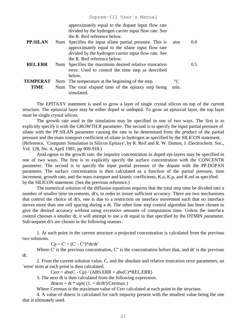
approximately equal to the dopant input flow ratedivided by the hydrogen carrier input flow rate. Seethe R. Reif reference below.
PP.SILAN Num Specifies the input silane partial pressure. This isapproximately equal to the silane input flow ratedivided by the hydrogen carrier input flow rate. Seethe R. Reif reference below.
atm 0.0
REL.ERR Num Specifies the maximum desired relative truncationerror. Used to control the time step as describedbelow.
0.5
TEMPERAT Num The temperature at the beginning of the step. °CTIME Num The total elapsed time of the epitaxy step being
simulated.min.
The EPITAXY statement is used to grow a layer of single crystal silicon on top of the currentstructure. The epitaxial layer may be either doped or undoped. To grow an epitaxial layer, the top layermust be single crystal silicon.
The growth rate used in the simulation may be specified in one of two ways. The first is toexplicitly specify it with the GROWTH.R parameter. The second is to specify the input partial pressure ofsilane with the PP.SILAN parameter causing the rate to be determined from the product of the partialpressure and the mass transport coefficient of silane in hydrogen as specified by the SILICON statement.(Reference, `Computer Simulation in Silicon Epitaxy', by R. Reif and R. W. Dutton, J. Electrochem. Soc.,Vol. 128, No. 4, April 1981, pp 909-918.)
AnaLogous to the growth rate, the impurity concentration in doped epi-layers may be specified inone of two ways. The first is to explicitly specify the surface concentration with the CONCENTRparameter. The second is to specify the input partial pressure of the dopant with the PP.DOPANparameter. The surface concentration is then calculated as a function of the partial pressure, timeincrement, growth rate, and the mass transport and kinetic coefficients, K.a, K.p, and K.mf as specifiedby the SILICON statement. (See the previous reference.)
The numerical solution of the diffusion equations requires that the total step time be divided into anumber of smaller time increments, dt's, in order to insure sufficient accuracy. There are two mechanismsthat control the choice of dt's, one is due to a restriction on interface movement such that no interfacemoves more than one cell spacing during a dt. The other time step control algorithm has been chosen togive the desired accuracy without using excessive amounts of computation time. Unless the interfacecontrol chooses a smaller dt, it will attempt to use a dt equal to that specified by the DTMIN parameter.Sub-sequent dt's are chosen in the following manner.
1. At each point in the current structure a projected concentration is calculated from the previoustwo solutions.
Cp = C' + (C' - C'')*dt/dt'Where C' is the previous concentration, C'' is the concentration before that, and dt' is the previous
dt.2. From the current solution value, C, and the absolute and relative truncation error parameters, an
`error' term at each point is then calculated.Cerr = abs(C - Cp) / (ABS.ERR + abs(C)*REL.ERR)
3. The next dt is then calculated from the following expression.dtnext = dt * sqrt( (1. + dt/dt')/Cerrmax )
Where Cerrmax is the maximum value of Cerr calculated at each point in the structure.4. A value of dtnext is calculated for each impurity present with the smallest value being the one
that is ultimately used.
Suprem-III User's Manual
22
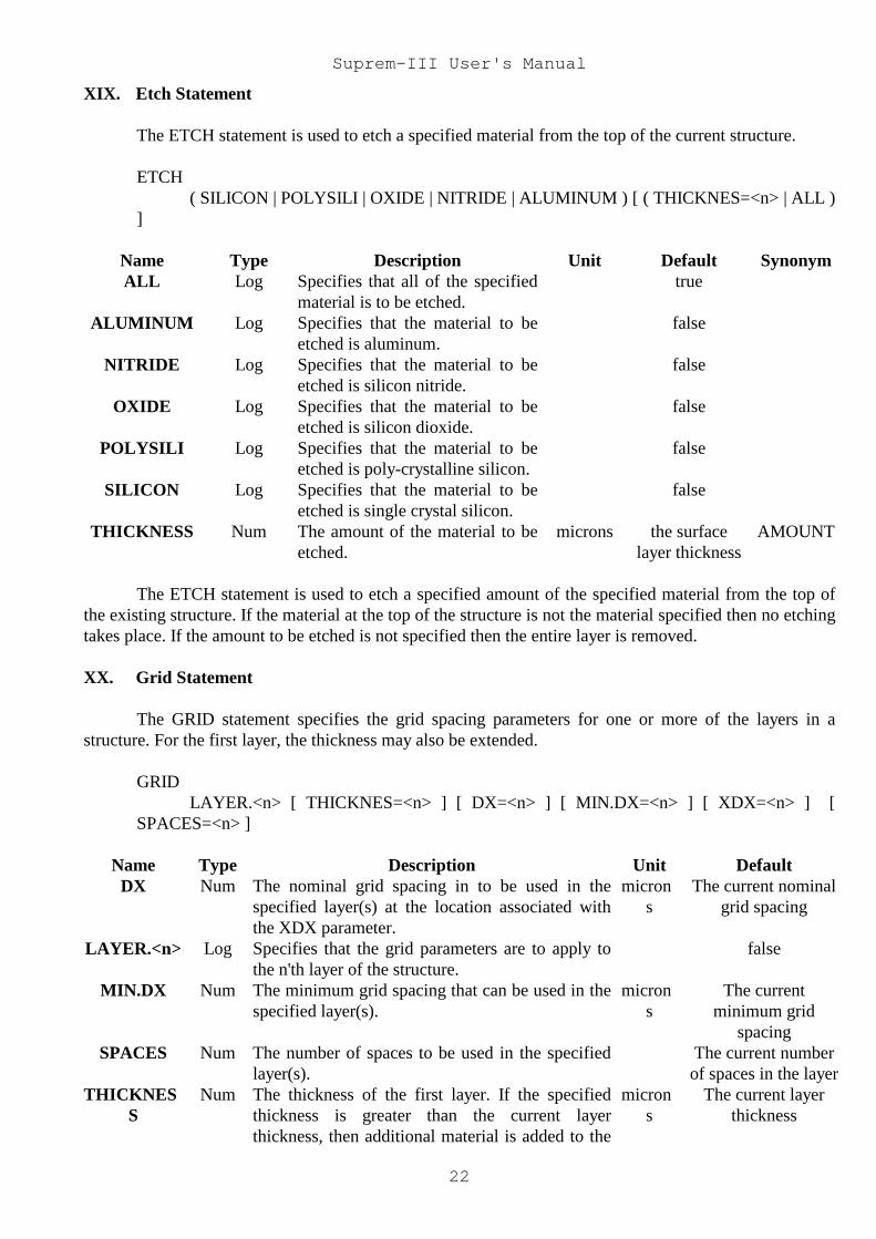
XIX. Etch Statement
The ETCH statement is used to etch a specified material from the top of the current structure.
ETCH( SILICON | POLYSILI | OXIDE | NITRIDE | ALUMINUM ) [ ( THICKNES=<n> | ALL )
]
Name Type Description Unit Default SynonymALL Log Specifies that all of the specified
material is to be etched.true
ALUMINUM Log Specifies that the material to beetched is aluminum.
false
NITRIDE Log Specifies that the material to beetched is silicon nitride.
false
OXIDE Log Specifies that the material to beetched is silicon dioxide.
false
POLYSILI Log Specifies that the material to beetched is poly-crystalline silicon.
false
SILICON Log Specifies that the material to beetched is single crystal silicon.
false
THICKNESS Num The amount of the material to beetched.
microns the surfacelayer thickness
AMOUNT
The ETCH statement is used to etch a specified amount of the specified material from the top ofthe existing structure. If the material at the top of the structure is not the material specified then no etchingtakes place. If the amount to be etched is not specified then the entire layer is removed.
XX. Grid Statement
The GRID statement specifies the grid spacing parameters for one or more of the layers in astructure. For the first layer, the thickness may also be extended.
GRIDLAYER.<n> [ THICKNES=<n> ] [ DX=<n> ] [ MIN.DX=<n> ] [ XDX=<n> ] [
SPACES=<n> ]
Name Type Description Unit DefaultDX Num The nominal grid spacing in to be used in the
specified layer(s) at the location associated withthe XDX parameter.
microns
The current nominalgrid spacing
LAYER.<n> Log Specifies that the grid parameters are to apply tothe n'th layer of the structure.
false
MIN.DX Num The minimum grid spacing that can be used in thespecified layer(s).
microns
The currentminimum grid
spacingSPACES Num The number of spaces to be used in the specified
layer(s).The current numberof spaces in the layer
THICKNESS
Num The thickness of the first layer. If the specifiedthickness is greater than the current layerthickness, then additional material is added to the
microns
The current layerthickness
Suprem-III User's Manual
23
bottom of the layer. The value specified must begreater than or equal to the current thickness.
XDX Num The distance from the surface of the layer at whichthe nominal grid spacing, DX, applies.
microns
The last valuespecified
The GRID statement is used primarily to change the grid spacing of one or more layers of thecurrent structure. In the case of the first, or bottom layer, the GRID statement may be used to extend thedepth of the layer by adding additional material to the bottom of the structure. In this case, the impurityconcentration at the bottommost cell in the structure is used uniformly in the added region.
XXI. Implant Statement
The IMPLANT statement is used to simulate the ion-implantation of impurities into the structure.Four types of implantation models are available, a numerical method based on the Boltzman transportequation, and three analytical methods based on simple Gaussian, two sided Gaussian, or Pearson type-IVdistributions.
IMPLANTDOSE=<n> ENERGY=<n> ( ANTIMONY | ARSENIC | BF2 | BORON | PHOSPHOR ) (
GAUSSIAN | 2-GAUSSI | PEARSON | ( BOLTZMAN [ MINSTEPS=<n> ] [ AT.WT=<n> ] [AT.NUMB=<n> ] ) )
Name Type Description Unit Default SynonymANTIMONY Log Specifies that the ion to be
implanted is antimony.false SB
ARSENIC Log Specifies that the ion to beimplanted is arsenic.
false AS
AT.NUMB Num The atomic number of the ion tobe implanted.
The last value specified inthe corresponding impurity
coefficient statementAT.WT Num The atomic weight of the ion to
be implanted.amu The last value specified in
the corresponding impuritycoefficient statement
AT.MASS
BF2 Log Specifies that the ion to beimplanted is boron-difluoride.
false
BOLTZMAN Log Specifies that the Boltzmantransport model is to be used insimulating the implantation.
false
BORON Log Specifies that the ion to beimplanted is atomic boron.
false
DOSE Num The implanted dose. atoms/cm2
ENERGY Num The energy of the implant beam. thousand eV
GAUSSIAN Log Specifies that a simple Gaussiandistribution is to be used tomodel the implanted profile.
false
MINSTEPS Num The minimum number of stepsbetween each grid point used incalculating the energydistribution during the solution
5.0
Suprem-III User's Manual
24
of the Boltzman transportequation.
PEARSON Log Specifies that a Pearson type-IVdistribution is to be used tomodel the implanted profile.
true, if no other model isspecified
PHOSPHOR Log Specifies that the ion to beimplanted is phosphorus.
false
2-GAUSSI Log Specifies that a two sidedGaussian distribution is to beused to model the implantedprofile.
false
The IMPLANT statement is used to simulate ion-implantation of impurities into the structure.Four different ion-implantation models are available.
When the BOLTZMANN option is selected, the implanted ion distribution is calculated by anumerical solution of the Boltzmann transport equation [1]. In this method, the momentum distribution ofthe implanted ion is determined at each depth in the target. Then distribution in energy and angle isrepresented numerically by a two-dimensional array (default size 15 x 8).
The calculation proceeds starting from the surface, where the momentum distribution is known tobe a delta function (mono-energetic beam moving normal to the target surface). A knowledge of thescattering cross section for both two-body atomic and electronic interactions, together with the transportequations, is then sufficient to determine how the momentum distribution evolves with depth. Materialdiscontinuities are simple to handle, since only the cross sections change as the ions cross any interface.When any ion scatters to an energy less than about 5% of the initial energy, or when an ion is scatteredback toward the target surface, that ion is considered stopped at that depth and becomes part of the rangedistribution.The calculation proceeds until the concentration of the implanted profile drops to 10-5 of itspeak value.
The other three models are based on fitting the as-implanted distribution to an analytical function.The three functions available are a simple Gaussian, a two sided Gaussian, or a Pearson type-IVdistribution. The necessary moments, or range statistics, are read from the implant moment data filespecified via the appropriate impuritys statement.
XXII. Impurity Statement
The IMPURITY statement is used to input or modify the physical or model coefficients associatedwith a dopant impurity.
IMPURITYINDEX=<n> [ NAME=<c> ] [ (DONOR | ACCEPTOR) ] [ AT.WT=<n> ] [
AT.NUMB=<n> ] [ IONFILE1=<c> ] [ IONFILE2=<c> ][ ( ( SILICON [ FII.0=<n> ] [ FII.E=<n> ] [ K.MF=<n> ] [ K.A=<n> ] [ K.P=<n> ] [
MISFITST=<n> ] [ CD=<n> ] [ MSF111FA=<n> ] [ MSF110FA=<n> ] [ MSF100FA=<n> ] [DAMAGEST=<n> ] [ NE.0=<n> ] [ NE.E=<n> ] [ ( IMPLANT | CHEMICAL ) [ CTN.0=<n> ] [CTN.E=<n> ] [ CTN.F=<n> ] ] ) | ( POLYSILI [ ENTROPY=<n> ] [ HEAT.SEG=<n> ] [Q.SITES=<n> ] [ FII.0=<n> ] [ FII.E=<n> ] [ ( IMPLANT | CHEMICAL ) [ CTN.0=<n> ] [CTN.E=<n> ] [ CTN.F=<n> ] ] ) | ( OXIDE | NITRIDE | ALUMINUM )
[ ELECT.ST=<n> ] [ DIX.0=<n> ] [ DIX.E=<n> ] [ DIM.0=<n> ] [ DIM.E=<n> ] [DIMM.0=<n> ] [ DIMM.E=<n> ] [ DIP.0=<n> ] [ DIP.E=<n> ] ]
Name Type Description Unit DefaultACCEPTOR Log Specifies that the impurity is an acceptor in false
Suprem-III User's Manual
25
silicon.ALUMINUM Log Specifies that the material dependent parameters
apply to the impurity in aluminum.false
AT.NUMB Num The atomic number of the impurity. the current valueAT.WT Num The atomic weight of the impurity. amu the current value
CD Num This parameter is used to calculate the temperaturedependent part of the expression for bandgapnarrowing due to lattice misfit strain from highconcentrations of phosphorus.
atoms/cm3
°C2current value
CHEMICAL Log Specifies that the clustering coefficients apply tothe impurity from a chemical source.
false
CTN.0 Num The pre-exponential constant used in calculatingthe impurity clustering coefficient.
atoms/cm3 the current value
CTN.E Num The activation energy used in calculating theimpurity clustering coefficient.
eV the current value
CTN.F Num The power dependence of the concentration usedin calculating the impurity clustering coefficient.
the current value
DAMAGEST Num The factor in the implant dose dependentexpression for calculating the bandgap narrowingdue to the residual damage of phosphorusimplants.
eV-cm1/2 the current value
DIM.0 Num The pre-exponential constant of the diffusioncoefficient of the impurity diffusing with singlynegative vacancies.
microns2/min.
the current value
DIM.E Num The activation energy of the diffusion coefficientof the impurity diffusing with singly negativevacancies.
eV the current value
DIMM.0 Num The pre-exponential constant of the diffusioncoefficient of the impurity diffusing with doublynegative vacancies.
microns2/min.
the current value
DIMM.E Num The activation energy of the diffusion coefficientof the impurity diffusing with doubly negativevacancies.
eV the current value
DIP.0 Num The pre-exponential constant of the diffusioncoefficient of the impurity diffusing with positivevacancies.
microns2/min.
the current value
DIP.E Num The activation energy of the diffusion coefficientof the impurity diffusing with positive vacancies.
eV the current value
DIX.0 Num The pre-exponential constant of the diffusioncoefficient of the impurity diffusing with neutralvacancies.
microns2/min.
the current value
DIX.E Num The activation energy of the diffusion coefficientof the impurity diffusing with neutral vacancies.
eV the current value
DONOR Log Specifies that the impurity is a donor in silicon. the current valueELECT.ST Num The electric stopping power of the impurity in the
specified material.KeV/micro
nthe current value
ENTROPY Num The entropy factor. Used to calculate theequilibrium segregation factor at polysilicon grainboundaries.
the current value
FII.0 Num The pre-exponential constant of the fractionalpartial-interstitialcy contribution.
(microns/minute)-1/2
the current value
Suprem-III User's Manual
26
FII.E Num The activation energy of the fractional partial-interstitialcy contribution.
eV the current value
HEAT.SEG Num The activation energy of the equilibriumsegregation factor at polysilicon grain boundaries.
eV the current value
IMPLANT Log Specifies that the impurity clustering coefficientsapply to the impurity from an implanted source.
false
IONFILE1 Char Specifies the primary ion implant range data filefor implants using the analytic distributions. Thisfile will be searched for the range statistics whenimplanting the atomic ion of this impurity.
the last filespecified
IONFILE2 Char Specifies the secondary ion implant range data filefor implants using the analytic distributions. Thisfile will be searched for the range statistics whenimplanting the compound ions containing thisimpurity.
the last filespecified
K.A Num Used in R. Reif's epitaxial doping model (seereference in EPITAXY statement). K.a is athermodynamic constant relating the dopantspecies concentration in solid silicon and adsorbedlayer.
cm the current value
K.MF Num Used in R. Reif's epitaxial doping model (seereference in EPITAXY statement). K.mf is akinetic coefficient controling the rate-limiting stepof the dopant incorporation process.
cm-2 min-1
atm-1the current value
K.P Num Used in R. Reif's epitaxial doping model (seereference in EPITAXY statement). K.p is athermodynamic constant relating the dopantspecies concentration in solid silicon and gasphase.
cm-3 atm-1 the current value
MISFITST Num The prefactor in the high concentration dependentexpression for calculating the bandgap narrowingdue to the lattice misfit strain from highconcentrations of phosphorus.
eV volts-cm-3
the current value
MSF100FA Num The orientation factor in <100> orientation siliconfor bandgap narrowing due to lattice misfit strainfrom high concentrations of phosphorus.
the current value
MSF110FA Num The orientation factor in <110> orientation siliconfor bandgap narrowing due to lattice misfit strainfrom high concentrations of phosphorus.
the current value
MSF111FA Num The orientation factor in <111> orientation siliconfor bandgap narrowing due to lattice misfit strainfrom high concentrations of phosphorus.
the current value
NAME Char The name of the impurity. the last namespecified
NE.0 Num The pre-exponential constant for Ne, theconcentration at which the P+V= pairsdisassociate. Used to calculate the diffusivity ofphosphorus at high concentrations.
atoms/cm3 the current value
NE.E Num The activation energy for calculating Ne, theconcentration at which the P+V= pairsdisassociate. Used to calculate the diffusivity of
eV the current value

Suprem-III User's Manual
27
phosphorus at high concentrations.NITRIDE Log Specifies that the material dependent parameters
apply to the impurity in silicon nitride.false
OXIDE Log Specifies that the material dependent parametersapply to the impurity in silicon dioxide.
false
POLYSILI Log Specifies that the material dependent parametersapply to the impurity in polysilicon.
false
Q.SITES Num Effective density of segregation sites at a grainboundary.
sites/cm2 the current value
SILICON Log Specifies that the material dependent parametersapply to the impurity in single crystal silicon.
false
The IMPURITY statement is used to input or modify the coefficients and parameters that define agiven impurity. Four impurities are defined, boron, phosphorus, arsenic, and antimony. These impuritieseach have their own impurity coefficient statements which are aliases of the general IMPURITYstatement.
XXIII. Initialize Statement
The INITIALIZE statement, as it's name implies, is used to set up the initial coefficients andstructure to be used in the processing steps that follow.
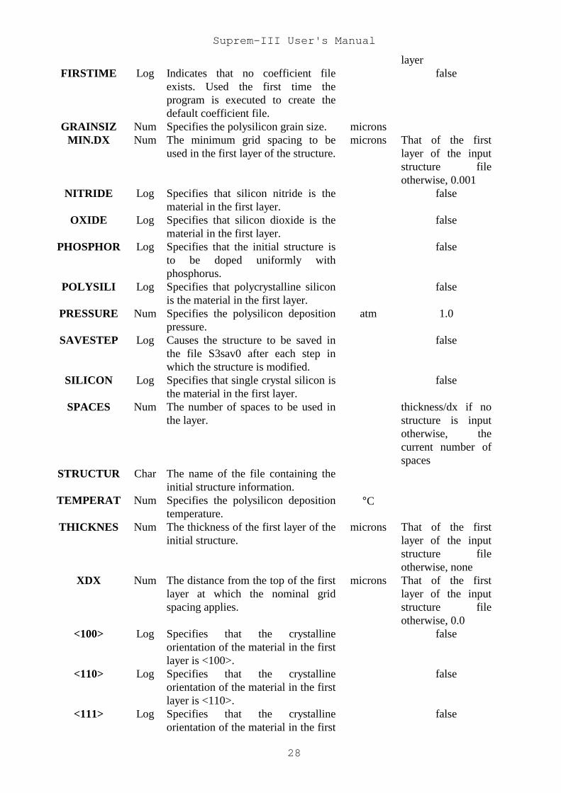
INITIALIZE[ ( COEFFICI=<c> | FIRSTIME ) ] [ STRUCTUR=<c> ] [ MIN.DX=<n> ] [ SAVESTEP ]
[ THICKNES=<n> ] [ DX=<n> ] [ XDX=<n> ] [ SPACES=<n> ][ ( SILICON ( <111> | <110> | <100> ) | POLYSILI ( GRAINSIZ=<n> | (
TEMPERAT=<n> [ PRESSURE=<n> ] ) ) | OXIDE | NITRIDE | ALUMINUM ) [CONCENTR=<n> ( ANTIMONY | ARSENIC | BORON | PHOSPHOR ) ] ]
Name Type Description Unit Default SynonymALUMINUM Log Specifies that aluminum is the
material in the first layer.false
ANTIMONY Log Specified that the initial structure isto be doped uniformly withantimony.
false SB
ARSENIC Log Specifies that the initial structure isto be doped uniformly with arsenic.
false AS
BORON Log Specifies that the initial structure isto be doped uniformly with boron.
false
COEFFICI Char The name of the file containing thephysical coefficients to be used bythe program.
S3cof0
CONCENTR Num The impurity concentration at whichthe structure is to be uniformlydoped.
atoms/cm3 0.0
DX Num The nominal grid spacing to be usedin the first layer of the structure atthe location specified by XDX.
microns That of the firstlayer of the inputstructure fileotherwise, thedefault for thematerial in the first
Suprem-III User's Manual
28
layerFIRSTIME Log Indicates that no coefficient file
exists. Used the first time theprogram is executed to create thedefault coefficient file.
false
GRAINSIZ Num Specifies the polysilicon grain size. micronsMIN.DX Num The minimum grid spacing to be
used in the first layer of the structure.microns That of the first
layer of the inputstructure fileotherwise, 0.001
NITRIDE Log Specifies that silicon nitride is thematerial in the first layer.
false
OXIDE Log Specifies that silicon dioxide is thematerial in the first layer.
false
PHOSPHOR Log Specifies that the initial structure isto be doped uniformly withphosphorus.
false
POLYSILI Log Specifies that polycrystalline siliconis the material in the first layer.
false
PRESSURE Num Specifies the polysilicon depositionpressure.
atm 1.0
SAVESTEP Log Causes the structure to be saved inthe file S3sav0 after each step inwhich the structure is modified.
false
SILICON Log Specifies that single crystal silicon isthe material in the first layer.
false
SPACES Num The number of spaces to be used inthe layer.
thickness/dx if nostructure is inputotherwise, thecurrent number ofspaces
STRUCTUR Char The name of the file containing theinitial structure information.
TEMPERAT Num Specifies the polysilicon depositiontemperature.
°C
THICKNES Num The thickness of the first layer of theinitial structure.
microns That of the firstlayer of the inputstructure fileotherwise, none
XDX Num The distance from the top of the firstlayer at which the nominal gridspacing applies.
microns That of the firstlayer of the inputstructure fileotherwise, 0.0
<100> Log Specifies that the crystallineorientation of the material in the firstlayer is <100>.
false
<110> Log Specifies that the crystallineorientation of the material in the firstlayer is <110>.
false
<111> Log Specifies that the crystallineorientation of the material in the first
false
Suprem-III User's Manual
29
layer is <111>.
An INITIALIZE statement is required in every SUPREM-III input sequence and it must preceedall other statements except for TITLE or COMMENT statements. At the start of execution the SUPREM-III program contains no information about any of the materials or impurities that may be used in theprocessing sequence. All of the physical and model coefficients and any initial structure information iscontained in one or two files and must be read into the programs internal storage before processing canproceed. Normally, all of the coefficient information is contained in a default file, S3COF0. If this is thecase, and if a coefficient file is not specified in the INITIALIZE statement, the data is read from thedefault coefficient file.
The same is true with the structure information, an initial structure of at least one layer of materialmust be present before execution can continue. A previously defined structure of arbitrary complexity canbe input from a file specified by the STRUCTUR parameter. The other parameters of the INITIALIZEstatement may be used to redefine the structure input from a file if the structure has only a single layer ofmaterial or, if no structure file is input, they may be used to set up the initial layer.
If no coefficient file is present, the FIRSTIME parameter must be specified and all of the neededcoefficients explicitly specified by subsequent statements before processing statements can be executed.As it's name implies, the FIRSTIME parameter should only be needed the first time the program isbrought up at a new installation.
XXIV. Loadfile Statement
The LOADFILE statement is used to input either a new structure to be processed, the physical andmodel coefficients to be used by the program, or both.
LOADFILEFILENAME=<c> ( ALL | COEFFICI | STRUCTUR )
Name Type Description Default SynonymALL Log Specifies that both the structure information and the
model coefficients are to be input from the specified file.false
COEFFICI Log Specifies that the coefficient information is to be inputfrom the specified file.
false
FILENAME Char The name of the file from which the specified informationis to be read.
NAME
STRUCTUR Log Specifies that the information describing the structure isto be input from the specified file.
false
The LOADFILE statement inputs two classes of information about the process that is to besimulated. The first class is the physical structure and impurity distributions of the materials to besimulated. This file is used as the starting point for subsequent processing steps. The other class ofinformation consists of all of the physical and model parameters or coefficients used by the program.
A LOADFILE statement may appear at any point in a processing sequence after the INITIALIZEstatement and before the STOP statement. If both structure and coefficient information are to be input, itis recommended that an INITIALIZE statement be used instead of LOADFILE.
XXV. Material Statement
The MATERIAL statement is used to input or modify the characteristics of a layer material. Theprogram is presently configured to handle up to ten different material types. Materials with index numbersone through five are defaulted to silicon, silicon dioxide, polysilicon, silicon nitride, and aluminum,
Suprem-III User's Manual
30
respectively. The parameter values for the defaulted materials may also be accessed via the SILICON,OXIDE, POLYSILI, NITRIDE, and ALUMINUM statements.
MATERIAL[ INDEX=<n> ] [ NAME=<c> ] [ DX.DEFAU=<n> ] [ ( SEMICOND | CONDUCTO |
INSULATO ) ] [ SPECIES=<n> ] [ DENSITY=<n> ] [ AT.WT.1=<n> ] [ AT.WT.2=<n> ] [AT.WT.3=<n> ] [ AT.NUM.1=<n> ] [ AT.NUM.2=<n> ] [ AT.NUM.3=<n> ] [ ABUND.1=<n> ][ ABUND.2=<n> ] [ ABUND.3=<n> ] [ DIFX.0=<n> ] [ DIFX.E=<n> ] [ DIMX.0=<n> ] [DIFM.E=<n> ] [ DIMMX.0=<n> ] [ DIFMM.E=<n> ] [ DIFP.0=<n> ] [ DIFP.E=<n> ] [NI.0=<n> ] [ NI.E=<n> ] [ NI.F=<n> ] [ DEFECTLN=<n> ] [ OEDK.0=<n> ] [ OEDK.E=<n> ] [OED.RATE=<n> ] [ 100.OEDF=<n> ] [ 110.OEDF=<n> ] [ 111.OEDF=<n> ] [ GSZ.H.0=<n> ] [GSZ.H.E=<n> ] [ GSZ.L.0=<n> ] [ GSZ.L.E=<n> ] [ MIN.GRAI=<n> ] [ TEMP.BRE=<n> ] [RATIO.0=<n> ] [ RATIO.E=<n> ] [ GEO.FACT=<n> ] [ GBE.0=<n> ] [ GBE.E=<n> ] [TAU.0=<n> ] [ TAU.E=<n> ] [ AFFINITY=<n> ] [ WORK.FUN=<n> ] [ EPSILONF=<n> ] [N.VALENC=<n> ] [ N.CONDUC=<n> ] [ BAND.GAP=<n> ] [ K.M=<n> ]
Name Type Description Unit DefaultABUND.1 Num The relative abundance of element one in the
material. The sum of all abundances for a materialmust equal one.
the current value
ABUND.2 Num The relative abundance of element two in thematerial. The sum of all abundances for a materialmust equal one.
the current value
ABUND.3 Num The relative abundance of element three in thematerial. The sum of all abundances for a materialmust equal one.
the current value
AFFINITY Num The electron affinity of the material. eV the current valueAT.NUM.1 Num The atomic number of element one in the
material.the current value
AT.NUM.2 Num The atomic number of element two in thematerial.
the current value
AT.NUM.3 Num The atomic number of element three in thematerial.
the current value
AT.WT.1 Num The atomic weight of element one in the material. amu the current valueAT.WT.2 Num The atomic weight of element two in the material. amu the current valueAT.WT.3 Num The atomic weight of element three in the
material.amu the current value
BAND.GAP Num The band gap of the material. eV the current valueCONDUCTO Num Specifies that the material is a conductor. falseDEFECTLN Num The decay length of point defects in the material. microns the current valueDENSITY Num The density of the material. grams/cm
3the current
value.DIFM.0 Num The pre-exponential constant used in the
calculation the component of the self-diffusivitydue to diffusion with singly negative vacancies.
microns2/min.
the current value
DIFM.E Num The activation energy used in the calculation thecomponent of the self-diffusivity due to diffusionwith singly negative vacancies.
eV the current value
DIFMM.0 Num The pre-exponential constant used in thecalculation of the component of the self-diffusivity due to diffusion with doubly negative
microns2/min.
the current value
Suprem-III User's Manual
31
vacancies.DIFMM.E Num The activation energy used in the calculation the
component of the self-diffusivity due to diffusionwith doubly negative vacancies.
eV the current value
DIFP.0 Num The pre-exponential constant used in thecalculation the component of the self-diffusivitydue to diffusion with positive vacancies.
microns2/min.
the current value
DIFP.E Num The activation energy used in the calculation thecomponent of the self-diffusivity due to diffusionwith positive vacancies.
eV the current value
DIFX.0 Num The pre-exponential constant used in thecalculation of the component of the self-diffusivity due to diffusion with neutralvacancies.
microns2/min.
the current value
DIFX.E Num The activation energy used in the calculation ofthe component of the self-diffusivity due todiffusion with neutral vacancies.
eV the current value
DX.DEFAU Num The default nominal grid spacing for any layercontaining this material.
microns the current value
EPSILONF Num The dielectric constant of the material relative thedielectric constant of air.
the current value
GBE.0 Num The pre-exponential constant used in calculatingthe grain-boundary energy
the current value
GBE.E Num The activation energy used in calculating thegrain-boundary energy.
eV the current value
GEO.FACT Num A geometric factor used in calculating the graingrowth driving force, F.
the current value
GSZ.H.0 Num The pre-exponential constant used in calculatingthe às deposited' polysilicon grain size forpressures near one atmosphere.
microns the current value
GSZ.H.E Num The activation energy used in calculating the àsdeposited' polysilicon grain size for pressures nearone atmosphere.
eV the current value
GSZ.L.0 Num The pre-exponential constant used in calculatingthe às deposited' polysilicon grain size for lowpressure CVD.
microns the current value
GSZ.L.E Num The activation energy used in calculating the `asdeposited' polysilicon grain size for low pressureCVD.
eV the current value
INDEX Num The material index of the material beingmodified. This number is used internally in theprogram to identify the material and point to itsparameters.
INSULATO Log Specifies that the material is an insulator. falseK.M Num Used in R. Reif's epitaxial growth model (see
reference in EPITAXY statement). K.m is themass transport coefficient for silane in hydrogen.
microns/min./atm
the current value
MIN.GRAI Num The minimum polysilicon grain size. Used for àsdeposited' LPCVD polysilicon when thetemperature is below that specified byTEMP.BRE
microns the current value
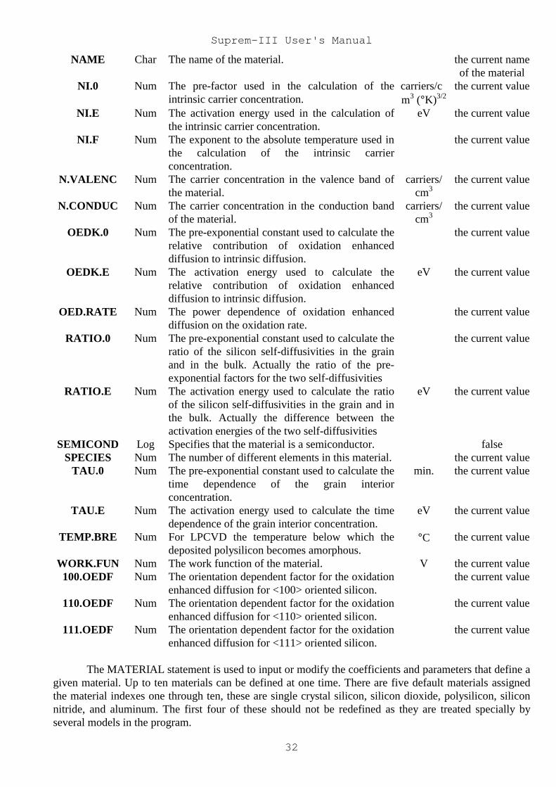
Suprem-III User's Manual
32
NAME Char The name of the material. the current nameof the material
NI.0 Num The pre-factor used in the calculation of theintrinsic carrier concentration.
carriers/cm3 (°K)3/2
the current value
NI.E Num The activation energy used in the calculation ofthe intrinsic carrier concentration.
eV the current value
NI.F Num The exponent to the absolute temperature used inthe calculation of the intrinsic carrierconcentration.
the current value
N.VALENC Num The carrier concentration in the valence band ofthe material.
carriers/cm3
the current value
N.CONDUC Num The carrier concentration in the conduction bandof the material.
carriers/cm3
the current value
OEDK.0 Num The pre-exponential constant used to calculate therelative contribution of oxidation enhanceddiffusion to intrinsic diffusion.
the current value
OEDK.E Num The activation energy used to calculate therelative contribution of oxidation enhanceddiffusion to intrinsic diffusion.
eV the current value
OED.RATE Num The power dependence of oxidation enhanceddiffusion on the oxidation rate.
the current value
RATIO.0 Num The pre-exponential constant used to calculate theratio of the silicon self-diffusivities in the grainand in the bulk. Actually the ratio of the pre-exponential factors for the two self-diffusivities
the current value
RATIO.E Num The activation energy used to calculate the ratioof the silicon self-diffusivities in the grain and inthe bulk. Actually the difference between theactivation energies of the two self-diffusivities
eV the current value
SEMICOND Log Specifies that the material is a semiconductor. falseSPECIES Num The number of different elements in this material. the current value
TAU.0 Num The pre-exponential constant used to calculate thetime dependence of the grain interiorconcentration.
min. the current value
TAU.E Num The activation energy used to calculate the timedependence of the grain interior concentration.
eV the current value
TEMP.BRE Num For LPCVD the temperature below which thedeposited polysilicon becomes amorphous.
°C the current value
WORK.FUN Num The work function of the material. V the current value100.OEDF Num The orientation dependent factor for the oxidation
enhanced diffusion for <100> oriented silicon.the current value
110.OEDF Num The orientation dependent factor for the oxidationenhanced diffusion for <110> oriented silicon.
the current value
111.OEDF Num The orientation dependent factor for the oxidationenhanced diffusion for <111> oriented silicon.
the current value
The MATERIAL statement is used to input or modify the coefficients and parameters that define agiven material. Up to ten materials can be defined at one time. There are five default materials assignedthe material indexes one through ten, these are single crystal silicon, silicon dioxide, polysilicon, siliconnitride, and aluminum. The first four of these should not be redefined as they are treated specially byseveral models in the program.
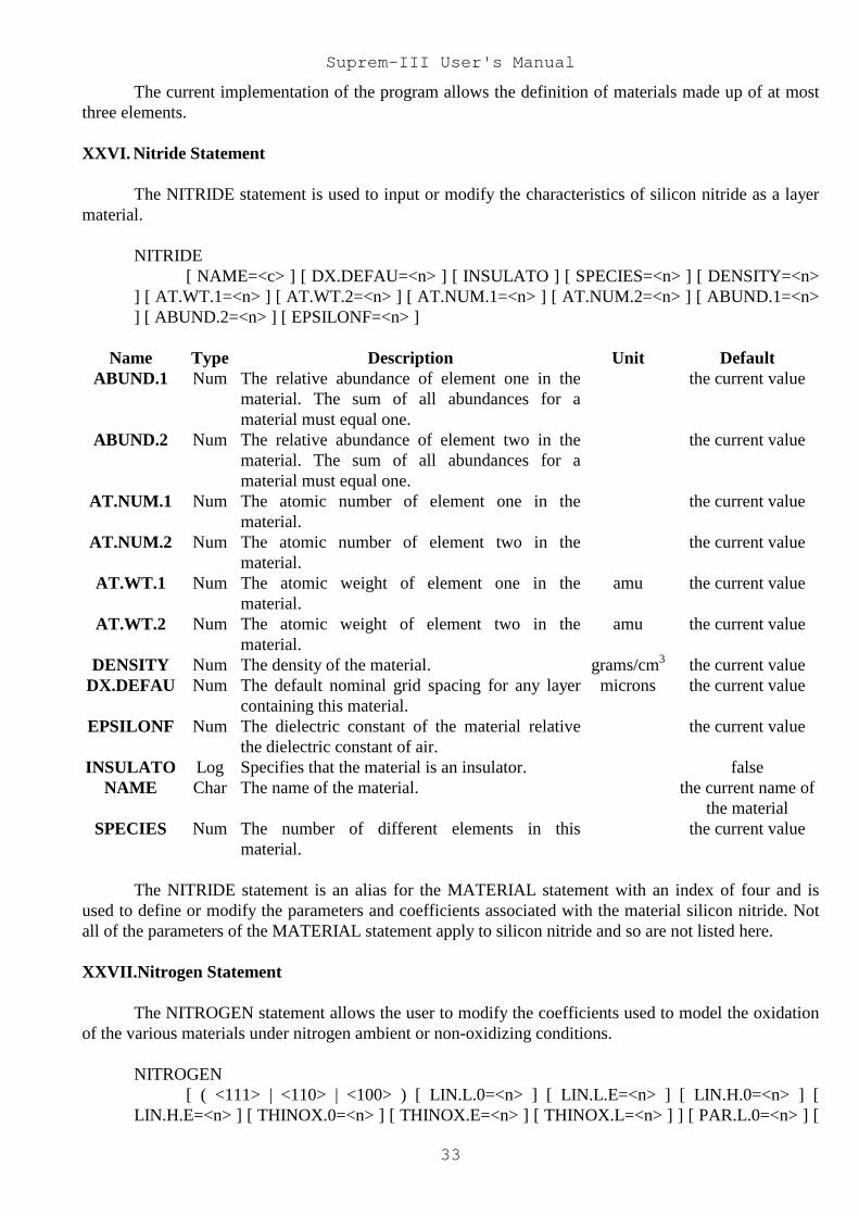
Suprem-III User's Manual
33
The current implementation of the program allows the definition of materials made up of at mostthree elements.
XXVI. Nitride Statement
The NITRIDE statement is used to input or modify the characteristics of silicon nitride as a layermaterial.
NITRIDE[ NAME=<c> ] [ DX.DEFAU=<n> ] [ INSULATO ] [ SPECIES=<n> ] [ DENSITY=<n>
] [ AT.WT.1=<n> ] [ AT.WT.2=<n> ] [ AT.NUM.1=<n> ] [ AT.NUM.2=<n> ] [ ABUND.1=<n>] [ ABUND.2=<n> ] [ EPSILONF=<n> ]
Name Type Description Unit DefaultABUND.1 Num The relative abundance of element one in the
material. The sum of all abundances for amaterial must equal one.
the current value
ABUND.2 Num The relative abundance of element two in thematerial. The sum of all abundances for amaterial must equal one.
the current value
AT.NUM.1 Num The atomic number of element one in thematerial.
the current value
AT.NUM.2 Num The atomic number of element two in thematerial.
the current value
AT.WT.1 Num The atomic weight of element one in thematerial.
amu the current value
AT.WT.2 Num The atomic weight of element two in thematerial.
amu the current value
DENSITY Num The density of the material. grams/cm3 the current valueDX.DEFAU Num The default nominal grid spacing for any layer
containing this material.microns the current value
EPSILONF Num The dielectric constant of the material relativethe dielectric constant of air.
the current value
INSULATO Log Specifies that the material is an insulator. falseNAME Char The name of the material. the current name of
the materialSPECIES Num The number of different elements in this
material.the current value
The NITRIDE statement is an alias for the MATERIAL statement with an index of four and isused to define or modify the parameters and coefficients associated with the material silicon nitride. Notall of the parameters of the MATERIAL statement apply to silicon nitride and so are not listed here.
XXVII. Nitrogen Statement
The NITROGEN statement allows the user to modify the coefficients used to model the oxidationof the various materials under nitrogen ambient or non-oxidizing conditions.
NITROGEN[ ( <111> | <110> | <100> ) [ LIN.L.0=<n> ] [ LIN.L.E=<n> ] [ LIN.H.0=<n> ] [
LIN.H.E=<n> ] [ THINOX.0=<n> ] [ THINOX.E=<n> ] [ THINOX.L=<n> ] ] [ PAR.L.0=<n> ] [
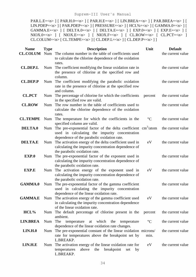
Suprem-III User's Manual
34
PAR.L.E=<n> ] [ PAR.H.0=<n> ] [ PAR.H.E=<n> ] [ LIN.BREA=<n> ] [ PAR.BREA=<n> ] [LIN.PDEP=<n> ] [ PAR.PDEP=<n> ] [ PRESSURE=<n> ] [ HCL%=<n> ] [ GAMMA.0=<n> ] [GAMMA.E=<n> ] [ DELTA.0=<n> ] [ DELTA.E=<n> ] [ EXP.0=<n> ] [ EXP.E=<n> ] [NIOX.0=<n> ] [ NIOX.E=<n> ] [ NIOX.F=<n> ] [ CL.ROW=<n> [ CL.PCT=<n> ]CL.COLUM=<n> [ CL.TEMPE=<n> ] [ CL.DEP.L=<n> ] [ CL.DEP.P=<n> ] ]
Name Type Description Unit DefaultCL.COLUM Num The column number in the table of coefficients used
to calculate the chlorine dependence of the oxidationrates.
the current value
CL.DEP.L Num The coefficient modifying the linear oxidation rate inthe presence of chlorine at the specified row andcolumn.
the current value
CL.DEP.P Num The coefficient modifying the parabolic oxidationrate in the presence of chlorine at the specified rowand column.
the current value
CL.PCT Num The percentage of chlorine for which the coefficientsin the specified row are valid.
percent the current value
CL.ROW Num The row number in the table of coefficients used tocalculate the chlorine dependence of the oxidationrates.
the current value
CL.TEMPE Num The temperature for which the coefficients in thespecified column are valid.
°C the current value
DELTA.0 Num The pre-exponential factor of the delta coefficientused in calculating the impurity concentrationdependence of the parabolic oxidation rate.
cm3/atom the current value
DELTA.E Num The activation energy of the delta coefficient used incalculating the impurity concentration dependence ofthe parabolic oxidation rate.
eV the current value
EXP.0 Num The pre-exponential factor of the exponent used incalculating the impurity concentration dependence ofthe parabolic oxidation rate.
the current value
EXP.E Num The activation energy of the exponent used incalculating the impurity concentration dependence ofthe parabolic oxidation rate.
eV the current value
GAMMA.0 Num The pre-exponential factor of the gamma coefficientused in calculating the impurity concentrationdependence of the linear oxidation rate.
the current value
GAMMA.E Num The activation energy of the gamma coefficient usedin calculating the impurity concentration dependenceof the linear oxidation rate.
eV the current value
HCL% Num The default percentage of chlorine present in theambient.
percent the current value
LIN.BREA Num The temperature at which the temperaturedependence of the linear oxidation rate changes.
°C the current value
LIN.H.0 Num The pre-exponential constant of the linear oxidationrate for temperatures above the breakpoint set byL.BREAKP.
microns/min.
the current value
LIN.H.E Num The activation energy of the linear oxidation rate fortemperatures above the breakpoint set byL.BREAKP.
eV the current value
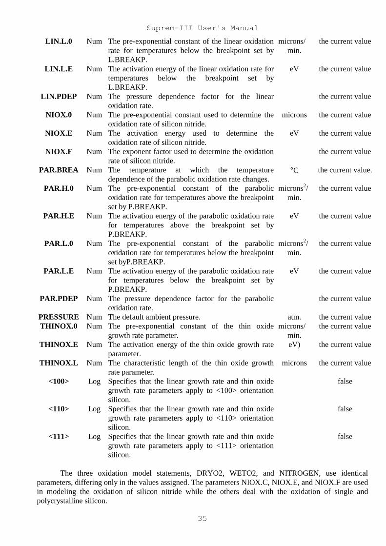
Suprem-III User's Manual
35
LIN.L.0 Num The pre-exponential constant of the linear oxidationrate for temperatures below the breakpoint set byL.BREAKP.
microns/min.
the current value
LIN.L.E Num The activation energy of the linear oxidation rate fortemperatures below the breakpoint set byL.BREAKP.
eV the current value
LIN.PDEP Num The pressure dependence factor for the linearoxidation rate.
the current value
NIOX.0 Num The pre-exponential constant used to determine theoxidation rate of silicon nitride.
microns the current value
NIOX.E Num The activation energy used to determine theoxidation rate of silicon nitride.
eV the current value
NIOX.F Num The exponent factor used to determine the oxidationrate of silicon nitride.
the current value
PAR.BREA Num The temperature at which the temperaturedependence of the parabolic oxidation rate changes.
°C the current value.
PAR.H.0 Num The pre-exponential constant of the parabolicoxidation rate for temperatures above the breakpointset by P.BREAKP.
microns2/min.
the current value
PAR.H.E Num The activation energy of the parabolic oxidation ratefor temperatures above the breakpoint set byP.BREAKP.
eV the current value
PAR.L.0 Num The pre-exponential constant of the parabolicoxidation rate for temperatures below the breakpointset byP.BREAKP.
microns2/min.
the current value
PAR.L.E Num The activation energy of the parabolic oxidation ratefor temperatures below the breakpoint set byP.BREAKP.
eV the current value
PAR.PDEP Num The pressure dependence factor for the parabolicoxidation rate.
the current value
PRESSURE Num The default ambient pressure. atm. the current valueTHINOX.0 Num The pre-exponential constant of the thin oxide
growth rate parameter.microns/
min.the current value
THINOX.E Num The activation energy of the thin oxide growth rateparameter.
eV) the current value
THINOX.L Num The characteristic length of the thin oxide growthrate parameter.
microns the current value
<100> Log Specifies that the linear growth rate and thin oxidegrowth rate parameters apply to <100> orientationsilicon.
false
<110> Log Specifies that the linear growth rate and thin oxidegrowth rate parameters apply to <110> orientationsilicon.
false
<111> Log Specifies that the linear growth rate and thin oxidegrowth rate parameters apply to <111> orientationsilicon.
false
The three oxidation model statements, DRYO2, WETO2, and NITROGEN, use identicalparameters, differing only in the values assigned. The parameters NIOX.C, NIOX.E, and NIOX.F are usedin modeling the oxidation of silicon nitride while the others deal with the oxidation of single andpolycrystalline silicon.
Suprem-III User's Manual
36
The effects of chlorine in the ambient gas on the oxidation rate of silicon are currently modeled byan empirical expression whose only variable is defined by the L.CLDEP and P.CLDEP for the linear andparabolic rates respectively. To date no convenient function is available to calculate the chlorinedependence as a function of temperature and amount of chlorine present, therefor a table of values definesthe chlorine dependence factors at those temperatures and percentages for which reliable data is available.For those temperatures and chlorine percentages between the values in the table, linear interpolation isemployed to calculate the value used. For temperatures or percentages outside the range of values presentin the table, the values whose conditions most nearly match the current conditions are used. For example,if the current conditions are a temperature of 1175 degrees with three percent chlorine, but the highesttemperature entry in the table is 1150 degrees and the nearest chlorine percentages are for two and fourpercent, then a value halfway between the values at 1150 degrees and two and four percent chlorine willbe used.
XXVIII. Oxide Statement
The OXIDE statement is used to input or modify the characteristics of silicon dioxide as a layermaterial.
OXIDE[ NAME=<c> ] [ DX.DEFAU=<n> ] [ INSULATO ] [ SPECIES=<n> ] [ DENSITY=<n>
] [ AT.WT.1=<n> ] [ AT.WT.2=<n> ] [ AT.NUM.1=<n> ] [ AT.NUM.2=<n> ] [ ABUND.1=<n>] [ ABUND.2=<n> ] [ EPSILONF=<n> ]
Name Type Description Unit DefaultABUND.1 Num The relative abundance of element one in the
material. The sum of all abundances for a materialmust equal one.
the current value
ABUND.2 Num The relative abundance of element two in thematerial. The sum of all abundances for a materialmust equal one.
the current value
AT.NUM.1 Num The atomic number of element one in the material. the current valueAT.NUM.2 Num The atomic number of element two in the material. the current valueAT.WT.1 Num The atomic weight of element one in the material. amu the current valueAT.WT.2 Num The atomic weight of element two in the material. amu the current valueDENSITY Num The density of the material. grams/cm
3the current value
DX.DEFAU Num The default nominal grid spacing for any layercontaining this material.
microns the current value
EPSILONF Num The dielectric constant of the material relative thedielectric constant of air.
the current value
INSULATO Log Specifies that the material is an insulator. falseNAME Char The name of the material. the current name
of the materialSPECIES Num The number of different elements in this material. the current value
The OXIDE statement is an alias for the MATERIAL statement with an index of two and is usedto define or modify the parameters and coefficients associated with the material silicon dioxide. Not all ofthe parameters of the MATERIAL statement apply to silicon dioxide and so are not listed here.
XXIX. Phosphorus Statement
Suprem-III User's Manual
37
The PHOSPHOR statement is used to input or modify the physical or model coefficientsassociated with phosphorus as a dopant impurity.
PHOSPHOR[ NAME=<c> ] [ DONOR ] [ AT.WT=<n> ] [ AT.NUMB=<n> ] [ IONFILE1=<c> ] [
IONFILE2=<c> ][ ( ( SILICON [ FII.0=<n> ] [ FII.E=<n> ] [ K.MF=<n> ] [ K.A=<n> ] [ K.P=<n> ] [
MISFITST=<n> ] [ CD=<n> ] [ MSF111FA=<n> ] [ MSF110FA=<n> ] [ MSF100FA=<n> ] [DAMAGEST=<n> ] [ NE.0=<n> ] [ NE.E=<n> ] [ ( IMPLANT | CHEMICAL ) [ CTN.0=<n> ] [CTN.E=<n> ] [ CTN.F=<n> ] ] ) | ( POLYSILI [ ENTROPY=<n> ] [ HEAT.SEG=<n> ] [Q.SITES=<n> ] [ FII.0=<n> ] [ FII.E=<n> ] [ ( IMPLANT | CHEMICAL ) [ CTN.0=<n> ] [CTN.E=<n> ] [ CTN.F=<n> ] ] ) | ( OXIDE | NITRIDE | ALUMINUM )
[ ELECT.ST=<n> ] [ DIX.0=<n> ] [ DIX.E=<n> ] [ DIM.0=<n> ] [ DIM.E=<n> ] [DIMM.0=<n> ] [ DIMM.E=<n> ] ]
Name Type Description Unit DefaultALUMINU
MLog Specifies that the material dependent parameters
apply to phosphorus in aluminum.false
AT.NUMB Num The atomic number of the impurity. the current valueAT.WT Num The atomic weight of the impurity. amu the current value
CD Num This parameter is used to calculate the temperaturedependent part of the expression for bandgapnarrowing due to lattice misfit strain from highconcentrations of phosphorus.
(atoms/cm3)(°C2)
the current value
CHEMICAL Log Specifies that the clustering coefficients apply tothe impurity from a chemical source.
false
CTN.0 Num The pre-exponential constant used in calculatingthe impurity clustering coefficient.
atoms/cm3
the current value
CTN.E Num The activation energy used in calculating theimpurity clustering coefficient.
eV the current value
CTN.F Num The power dependence of the concentration used incalculating the impurity clustering coefficient.
the current value
DAMAGEST
Num The factor in the implant dose dependentexpression for calculating the bandgap narrowingdue to the residual damage of phosphorus implants.
eV cm1/2 the current value
DIM.0 Num The pre-exponential constant of the diffusioncoefficient of the impurity diffusing with singlynegative vacancies.
microns2
/min.the current value
DIM.E Num The activation energy of the diffusion coefficientof the impurity diffusing with singly negativevacancies.
eV the current value
DIMM.0 Num The pre-exponential constant of the diffusioncoefficient of the impurity diffusing with doublynegative vacancies.
microns2
/min.the current value
DIMM.E Num The activation energy of the diffusion coefficientof the impurity diffusing with doubly negativevacancies.
eV the current value
DIX.0 Num The pre-exponential constant of the diffusioncoefficient of the impurity diffusing with neutralvacancies.
microns2
/min.the current value
DIX.E Num The activation energy of the diffusion coefficient eV the current value
Suprem-III User's Manual
38
of the impurity diffusing with neutral vacancies.DONOR Log Specifies that the impurity is a donor in silicon. the current value
ELECT.ST Num The electric stopping power of the impurity in thespecified material.
KeV/micron.
the current value
ENTROPY Num The entropy factor. Used to calculate theequilibrium segregation factor at polysilicon grainboundaries.
the current value
FII.0 Num The pre-exponential constant of the fractionalpartial-interstitialcy contribution.
(microns/min.)-1/2
the current value
FII.E Num The activation energy of the fractional partial-interstitialcy contribution.
eV the current value
HEAT.SEG Num The activation energy of the equilibriumsegregation factor at polysilicon grain boundaries.
eV the current value
IMPLANT Log Specifies that the impurity clustering coefficientsapply to the impurity from an implanted source.
false
IONFILE1 Char Specifies the primary ion implant range data filefor implants using the analytic distributions. Thisfile will be searched for the range statistics whenimplanting atomic phosphorus.
the last file specified
IONFILE2 Char Specifies the secondary ion implant range data filefor implants using the analytic distributions. Thisfile will be searched for the range statistics whenimplanting the compound ions containingphosphorus.
the last file specified
K.A Num Used in R. Reif's epitaxial doping model (seereference in EPITAXY statement). K.a is athermodynamic constant relating the dopantspecies concentration in solid silicon and adsorbedlayer.
cm the current value
K.MF Num Used in R. Reif's epitaxial doping model (seereference in EPITAXY statement). K.mf is akinetic coefficient controlling the rate-limiting stepof the dopant incorporation process.
cm-2
min-1
atm-1
the current value
K.P Num Used in R. Reif's epitaxial doping model (seereference in EPITAXY statement). K.p is athermodynamic constant relating the dopantspecies concentration in solid silicon and gasphase.
cm-3
atm-1the current value
MISFITST Num The prefactor in the high concentration dependentexpression for calculating the bandgap narrowingdue to the lattice misfit strain from highconcentrations of phosphorus.
eV-cm3 the current value
MSF100FA Num The orientation factor in <100> orientation siliconfor bandgap narrowing due to lattice misfit strainfrom high concentrations of phosphorus.
the current value
MSF110FA Num The orientation factor in <110> orientation siliconfor bandgap narrowing due to lattice misfit strainfrom high concentrations of phosphorus.
the current value
MSF111FA Num The orientation factor in <111> orientation siliconfor bandgap narrowing due to lattice misfit strainfrom high concentrations of phosphorus.
the current value
Suprem-III User's Manual
39
NAME Char The name of the impurity. the last namespecified
NE.0 Num The pre-exponential constant for Ne, theconcentration at which the P+V= pairsdisassociate. Used to calculate the diffusivity ofphosphorus at high concentrations.
atoms/cm3
the current value
NE.E Num The activation energy for calculating Ne, theconcentration at which the P+V= pairsdisassociate. Used to calculate the diffusivity ofphosphorus at high concentrations.
eV the current value
NITRIDE Log Specifies that the material dependent parametersapply to phosphorus in silicon nitride.
false
OXIDE Log Specifies that the material dependent parametersapply to phosphorus in silicon dioxide.
false
POLYSILI Log Specifies that the material dependent parametersapply to phosphorus in polysilicon.
false
Q.SITES Num Effective density of segregation sites at a grainboundary.
sites/cm2
the current value
SILICON Log Specifies that the material dependent parametersapply to phosphorus in silicon.
false
The PHOSPHOR statement is an alias for the IMPURITY statement with an index of two and isused to define or modify the parameters and coefficients associated with phosphorus as an impurity. Notall of the parameters of the IMPURITY statement apply to phosphorus and so are not listed here.
XXX. Plot Statement
The PLOT statement outputs a semi-Logarithmic plot of the specified impurity concentrationsversus depth into the structure.
PLOT[ ACTIVE ] [ CHEMICAL ] [ TOTAL ] [ NET ] [ ANTIMONY ] [ ARSENIC ] [ BORON
] [ PHOSPHOR ] [ XMIN=<n> ] [ XMAX=<n> ] [ CMIN=<n> ] [ CMAX=<n> ][ ( ( HP2648A | HP2623A ) [ CLEAR ] [ AXIS ] [ XPWIDTH=<n> ] [ YPWIDTH=<n> ] [
XPTS.IN=<n> ] [ YPTS.IN=<n> ] [ XOFSET=<n> ] [ YOFSET=<n> ] ] [ LINETYPE=<n> ] [FILENAME=<c> ] ) | ( LP.PLOT [ LINES/PA=<n> ] [ COLUMNS=<n> ] ) ]
Name Type Description Unit Default SynonymACTIVE Log Specifies that the electrically active
concentrations of the specified impurities are tobe plotted.
false
ANTIMONY
Log Specifies that the antimony concentration, eitheractive and/or chemical, is to be plotted.
false SB
ARSENIC Log Specifies that the arsenic concentration, eitheractive and/or chemical, is to be plotted.
false AS
AXIS Log Specifies that the axis is to be plotted. Not usedby line printer plots.
true
BORON Log Specifies that the boron concentration, eitheractive and/or chemical, is to be plotted.
false
CHEMICAL Log Specifies that the chemical concentration of thespecified impurities are to be plotted.
false
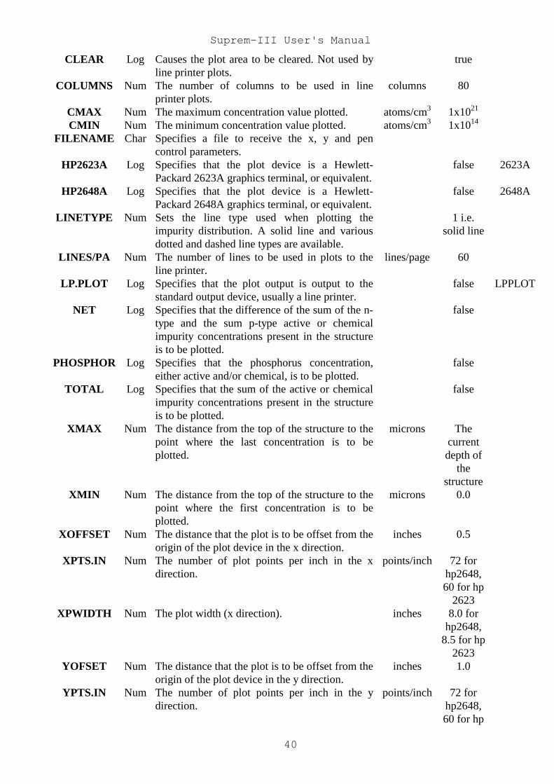
Suprem-III User's Manual
40
CLEAR Log Causes the plot area to be cleared. Not used byline printer plots.
true
COLUMNS Num The number of columns to be used in lineprinter plots.
columns 80
CMAX Num The maximum concentration value plotted. atoms/cm3 1x10²¹
CMIN Num The minimum concentration value plotted. atoms/cm3 1x10¹⁴
FILENAME Char Specifies a file to receive the x, y and pencontrol parameters.
HP2623A Log Specifies that the plot device is a Hewlett-Packard 2623A graphics terminal, or equivalent.
false 2623A
HP2648A Log Specifies that the plot device is a Hewlett-Packard 2648A graphics terminal, or equivalent.
false 2648A
LINETYPE Num Sets the line type used when plotting theimpurity distribution. A solid line and variousdotted and dashed line types are available.
1 i.e.solid line
LINES/PA Num The number of lines to be used in plots to theline printer.
lines/page 60
LP.PLOT Log Specifies that the plot output is output to thestandard output device, usually a line printer.
false LPPLOT
NET Log Specifies that the difference of the sum of the n-type and the sum p-type active or chemicalimpurity concentrations present in the structureis to be plotted.
false
PHOSPHOR Log Specifies that the phosphorus concentration,either active and/or chemical, is to be plotted.
false
TOTAL Log Specifies that the sum of the active or chemicalimpurity concentrations present in the structureis to be plotted.
false
XMAX Num The distance from the top of the structure to thepoint where the last concentration is to beplotted.
microns Thecurrentdepth of
thestructure
XMIN Num The distance from the top of the structure to thepoint where the first concentration is to beplotted.
microns 0.0
XOFFSET Num The distance that the plot is to be offset from theorigin of the plot device in the x direction.
inches 0.5
XPTS.IN Num The number of plot points per inch in the xdirection.
points/inch 72 forhp2648,60 for hp
2623XPWIDTH Num The plot width (x direction). inches 8.0 for
hp2648,8.5 for hp
2623YOFSET Num The distance that the plot is to be offset from the
origin of the plot device in the y direction.inches 1.0
YPTS.IN Num The number of plot points per inch in the ydirection.
points/inch 72 forhp2648,60 for hp
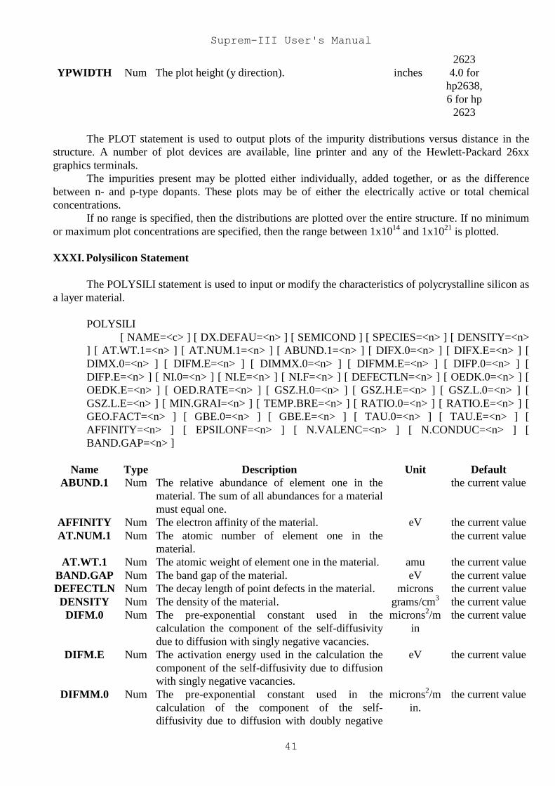
Suprem-III User's Manual
41
2623YPWIDTH Num The plot height (y direction). inches 4.0 for
hp2638,6 for hp
2623
The PLOT statement is used to output plots of the impurity distributions versus distance in thestructure. A number of plot devices are available, line printer and any of the Hewlett-Packard 26xxgraphics terminals.
The impurities present may be plotted either individually, added together, or as the differencebetween n- and p-type dopants. These plots may be of either the electrically active or total chemicalconcentrations.
If no range is specified, then the distributions are plotted over the entire structure. If no minimumor maximum plot concentrations are specified, then the range between 1x10¹⁴ and 1x10²¹ is plotted.
XXXI. Polysilicon Statement
The POLYSILI statement is used to input or modify the characteristics of polycrystalline silicon asa layer material.
POLYSILI[ NAME=<c> ] [ DX.DEFAU=<n> ] [ SEMICOND ] [ SPECIES=<n> ] [ DENSITY=<n>
] [ AT.WT.1=<n> ] [ AT.NUM.1=<n> ] [ ABUND.1=<n> ] [ DIFX.0=<n> ] [ DIFX.E=<n> ] [DIMX.0=<n> ] [ DIFM.E=<n> ] [ DIMMX.0=<n> ] [ DIFMM.E=<n> ] [ DIFP.0=<n> ] [DIFP.E=<n> ] [ NI.0=<n> ] [ NI.E=<n> ] [ NI.F=<n> ] [ DEFECTLN=<n> ] [ OEDK.0=<n> ] [OEDK.E=<n> ] [ OED.RATE=<n> ] [ GSZ.H.0=<n> ] [ GSZ.H.E=<n> ] [ GSZ.L.0=<n> ] [GSZ.L.E=<n> ] [ MIN.GRAI=<n> ] [ TEMP.BRE=<n> ] [ RATIO.0=<n> ] [ RATIO.E=<n> ] [GEO.FACT=<n> ] [ GBE.0=<n> ] [ GBE.E=<n> ] [ TAU.0=<n> ] [ TAU.E=<n> ] [AFFINITY=<n> ] [ EPSILONF=<n> ] [ N.VALENC=<n> ] [ N.CONDUC=<n> ] [BAND.GAP=<n> ]
Name Type Description Unit DefaultABUND.1 Num The relative abundance of element one in the
material. The sum of all abundances for a materialmust equal one.
the current value
AFFINITY Num The electron affinity of the material. eV the current valueAT.NUM.1 Num The atomic number of element one in the
material.the current value
AT.WT.1 Num The atomic weight of element one in the material. amu the current valueBAND.GAP Num The band gap of the material. eV the current valueDEFECTLN Num The decay length of point defects in the material. microns the current valueDENSITY Num The density of the material. grams/cm3 the current value
DIFM.0 Num The pre-exponential constant used in thecalculation the component of the self-diffusivitydue to diffusion with singly negative vacancies.
microns2/min
the current value
DIFM.E Num The activation energy used in the calculation thecomponent of the self-diffusivity due to diffusionwith singly negative vacancies.
eV the current value
DIFMM.0 Num The pre-exponential constant used in thecalculation of the component of the self-diffusivity due to diffusion with doubly negative
microns2/min.
the current value
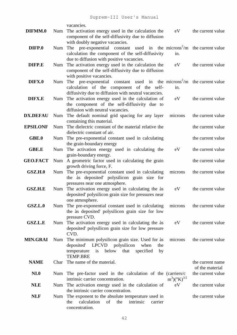
Suprem-III User's Manual
42
vacancies.DIFMM.0 Num The activation energy used in the calculation the
component of the self-diffusivity due to diffusionwith doubly negative vacancies.
eV the current value
DIFP.0 Num The pre-exponential constant used in thecalculation the component of the self-diffusivitydue to diffusion with positive vacancies.
microns2/min.
the current value
DIFP.E Num The activation energy used in the calculation thecomponent of the self-diffusivity due to diffusionwith positive vacancies.
eV the current value
DIFX.0 Num The pre-exponential constant used in thecalculation of the component of the self-diffusivity due to diffusion with neutral vacancies.
microns2/min.
the current value
DIFX.E Num The activation energy used in the calculation ofthe component of the self-diffusivity due todiffusion with neutral vacancies.
eV the current value
DX.DEFAU Num The default nominal grid spacing for any layercontaining this material.
microns the current value
EPSILONF Num The dielectric constant of the material relative thedielectric constant of air.
the current value
GBE.0 Num The pre-exponential constant used in calculatingthe grain-boundary energy
the current value
GBE.E Num The activation energy used in calculating thegrain-boundary energy.
eV the current value
GEO.FACT Num A geometric factor used in calculating the graingrowth driving force, F.
the current value
GSZ.H.0 Num The pre-exponential constant used in calculatingthe às deposited' polysilicon grain size forpressures near one atmosphere.
microns the current value
GSZ.H.E Num The activation energy used in calculating the àsdeposited' polysilicon grain size for pressures nearone atmosphere.
eV the current value
GSZ.L.0 Num The pre-exponential constant used in calculatingthe às deposited' polysilicon grain size for lowpressure CVD.
microns the current value
GSZ.L.E Num The activation energy used in calculating the àsdeposited' polysilicon grain size for low pressureCVD.
eV the current value
MIN.GRAI Num The minimum polysilicon grain size. Used for àsdeposited' LPCVD polysilicon when thetemperature is below that specified byTEMP.BRE
microns the current value
NAME Char The name of the material. the current nameof the material
NI.0 Num The pre-factor used in the calculation of theintrinsic carrier concentration.
(carriers/cm3)(°K)3/2
the current value
NI.E Num The activation energy used in the calculation ofthe intrinsic carrier concentration.
eV the current value
NI.F Num The exponent to the absolute temperature used inthe calculation of the intrinsic carrierconcentration.
the current value

Suprem-III User's Manual
43
N.CONDUC Num The carrier concentration in the conduction bandof the material.
carriers/cm3
the current value
N.VALENC Num The carrier concentration in the valence band ofthe material.
carriers/cm3
the current value
OEDK.0 Num The pre-exponential constant used to calculate therelative contribution of oxidation enhanceddiffusion to intrinsic diffusion.
the current value
OEDK.E Num The activation energy used to calculate therelative contribution of oxidation enhanceddiffusion to intrinsic diffusion.
eV the current value
OED.RATE Num The power dependence of oxidation enhanceddiffusion on the oxidation rate.
the current value
RATIO.0 Num The pre-exponential constant used to calculate theratio of the silicon self-diffusivities in the grainand in the bulk. Actually the ratio of the pre-exponential factors for the two self-diffusivities
the current value
RATIO.E Num The activation energy used to calculate the ratio ofthe silicon self-diffusivities in the grain and in thebulk. Actually the difference between theactivation energies of the two self-diffusivities
eV the current value
SEMICOND Log Specifies that the material is a semiconductor. falseSPECIES Num The number of different elements in this material. the current value
TAU.0 Num The pre-exponential constant used to calculate thetime dependence of the grain interiorconcentration.
min. the current value
TAU.E Num The activation energy used to calculate the timedependence of the grain interior concentration.
eV the current value
TEMP.BRE Num For LPCVD the temperature below which thedeposited polysilicon becomes amorphous.
°C the current value
The POLYSILI statement is an alias for the MATERIAL statement with an index of three and isused to define or modify the parameters and coefficients associated with the material polysilicon. Not allof the parameters of the MATERIAL statement apply to polysilicon and so are not listed here.
XXXII. Print Statement
The PRINT statement outputs information about the structure being simulated and the coefficientsused in the simulation. The printed out-put may consist of the impurity concentrations versus depth intothe structure, junction depths, sheet resistivities, layer thicknesses, diffusion or oxidation rates, etc.
PRINT[ CONCENTR [ ACTIVE ] [ CHEMICAL ] [ ALL ] [ TOTAL ] [ NET ] [ ANTIMONY ] [
ARSENIC ] [ BORON ] [ PHOSPHOR ] [ XMIN=<n> ] [ XMAX=<n> ] ] [ IMPURITY [ ALL | (ANTIMONY | ARSENIC | BORON | PHOSPHOR ) ] ]
[ MATERIAL [ ALL | ( SILICON | POLYSILI | OXIDE | NITRIDE | ALUMINUM ) ] ][ LAYERS ] [ SEGREGAT ] [ OXIDATIO ] [ LINES/PA=<n> ] [ COLUMNS=<n> ] [ LU=<n> |
FILENAME=<c> ]
Name Type Description Unit Default SynonymACTIVE Log Specifies that the electrically active concentration
of the specified impurities are to be printed.false
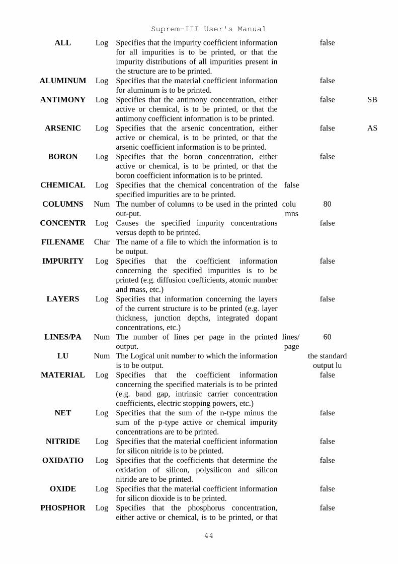
Suprem-III User's Manual
44
ALL Log Specifies that the impurity coefficient informationfor all impurities is to be printed, or that theimpurity distributions of all impurities present inthe structure are to be printed.
false
ALUMINUM Log Specifies that the material coefficient informationfor aluminum is to be printed.
false
ANTIMONY Log Specifies that the antimony concentration, eitheractive or chemical, is to be printed, or that theantimony coefficient information is to be printed.
false SB
ARSENIC Log Specifies that the arsenic concentration, eitheractive or chemical, is to be printed, or that thearsenic coefficient information is to be printed.
false AS
BORON Log Specifies that the boron concentration, eitheractive or chemical, is to be printed, or that theboron coefficient information is to be printed.
false
CHEMICAL Log Specifies that the chemical concentration of thespecified impurities are to be printed.
false
COLUMNS Num The number of columns to be used in the printedout-put.
columns
80
CONCENTR Log Causes the specified impurity concentrationsversus depth to be printed.
false
FILENAME Char The name of a file to which the information is tobe output.
IMPURITY Log Specifies that the coefficient informationconcerning the specified impurities is to beprinted (e.g. diffusion coefficients, atomic numberand mass, etc.)
false
LAYERS Log Specifies that information concerning the layersof the current structure is to be printed (e.g. layerthickness, junction depths, integrated dopantconcentrations, etc.)
false
LINES/PA Num The number of lines per page in the printedoutput.
lines/page
60
LU Num The Logical unit number to which the informationis to be output.
the standardoutput lu
MATERIAL Log Specifies that the coefficient informationconcerning the specified materials is to be printed(e.g. band gap, intrinsic carrier concentrationcoefficients, electric stopping powers, etc.)
false
NET Log Specifies that the sum of the n-type minus thesum of the p-type active or chemical impurityconcentrations are to be printed.
false
NITRIDE Log Specifies that the material coefficient informationfor silicon nitride is to be printed.
false
OXIDATIO Log Specifies that the coefficients that determine theoxidation of silicon, polysilicon and siliconnitride are to be printed.
false
OXIDE Log Specifies that the material coefficient informationfor silicon dioxide is to be printed.
false
PHOSPHOR Log Specifies that the phosphorus concentration,either active or chemical, is to be printed, or that
false
Suprem-III User's Manual
45
the phosphorus coefficient information is to beprinted.
POLYSILI Log Specifies that the material coefficient informationfor polysilicon is to be printed.
false
SEGREGAT Log Specifies that the coefficients that determine thesegregation of impurities across materialinterfaces are to be printed. The mass transportcoefficients and the volume ratios are alsoprinted.
false
SILICON Log Specifies that the material coefficient informationfor single crystal silicon is to be printed.
false
TOTAL Log Specifies that the sum of all of the active orchemical impurity concentrations present in thestructure is to be printed.
false
XMAX Num The distance from the top of the structure to thepoint where the last concentration is to be printed.
microns
The currentdepth of the
structureXMIN Num The distance from the top of the structure to the
point where the first concentration is to beprinted.
microns
0.0
The PRINT statement is used to output printed information. This information may consist ofstructural information such as junction depths, layer thicknesses or various impurity distributions versusdistance in the structure, or coefficient information such as the coefficients for impurity diffusion orsegregation, the oxidation of silicon, or the atomic number and mass of impurities or materials.
The impurities present may be printed either individually, added together, or as the differencebetween n- and p-type dopants. These prints may be of either electrically or total chemical concentrations.
If no range is specified, then the distributions are printed over the entire structure.Normally the output of the print statement goes to the standard output device (usually the line
printer), but the user may override the output Logical unit number by specifying the output lu, or he maydirect it into a specified file.
XXXIII. Profile Statement
The PROFILE statement is used to input an arbitrary impurity profile from a data file. The datamust be stored as two columns, one being the distance from the origin and the other being theconcentration at that point.
PROFILEFILE=<c> CONC.COL=<n> X.COL=<n> [ LAYER=<n> ] [ SKIP=<n> ] [
COUNT=<n> ] [ COM.CHAR=<c> ] ( ANTIMONY | ARSENIC | BORON | PHOSPHOR )
Name Type Description Default SynonymANTIMONY Log Specifies that the profile data is for the dopant
antimony.false SB
ARSENIC Log Specifies that the profile data is for the dopant arsenic. false ASBORON Log Specifies that the profile data is for the dopant boron. false
COM.CHAR Char Specifies the comment character for the lines in the file.Any line with this character in column one is ignored.
*
CONC.COL Num Specifies the column in the file containing theconcentration data.
Suprem-III User's Manual
46
COUNT Num Specifies the number of data points to be input. Input all everydata point.
LAYER Num Specifies the layer at which the first data point is to beplaced.
Topmost layer
PHOSPHOR Log Specifies that the profile data is for the dopantphosphorus.
false
SKIP Num Specifies the number of data points to be skipped oninput.
0
X.COL Num Specifies the column in the file containing the distanceof each data point from the origin.
The PROFILE statement inputs an arbitrary impurity distribution of the specified dopant from adata file. The data files must be organized in columns, with one column containing the concentration dataand another containing the distance from the origin at which the corresponding concentration applies. Thedata in the columns must be organized such that the locations are in increasing order. Comment lines mayappear at any point as long as they are preceded the comment character in column one.
XXXIV. Resistivity Statement
The RESISTIVITY statement is used to input a table of ordered resistivity/concentration pairs.This data is used by the program to calculate the resistivity of diffused layers in the current structure.
RESISTIVITYFILE=<c> CONC.COL=<n> RES.COL=<n> [ SKIP=<n> ] [ COUNT=<n> ] [
COM.CHAR=<c> ] ( ANTIMONY | ARSENIC | BORON | PHOSPHOR ) ( ALUMINUM |NITRIDE | OXIDE | POLYSILICON | SILICON )
Name Type Description Default SynonymALUMINUM Log Specifies that the resistivity data applies to the
impurity in the material aluminum.false
ANTIMONY Log Specifies that the resistivity data applies to the dopantantimony.
false SB
ARSENIC Log Specifies that the resistivity data applies to the dopantarsenic.
false AS
BORON Log Specifies that the resistivity data applies to the dopantboron.
false
COM.CHAR Char Specifies the comment character for the lines in thefile. Any line with this character in column one isignored.
*
CONC.COL Num Specifies the column in the data file containing theconcentrations at which the resistivity data applies.
CON.COL
COUNT Num Specifies the number of data points to be input. Input all everydata point
NITRIDE Log Specifies that the resistivity data applies to theimpurity in the material nitride.
false
OXIDE Log Specifies that the resistivity data applies to theimpurity in the material oxide.
false
PHOSPHOR Log Specifies that the resistivity data applies to the dopantphosphorus.
false
POLYSILI Log Specifies that the resistivity data applies to theimpurity in the material polysilicon.
false
Suprem-III User's Manual
47
RES.COL Num Specifies the column in the data file containing theresistivities associated with the correspondingconcentration values.
SKIP Num Specifies the number of data points to be skipped oninput.
0
SILICON Log Specifies that the resistivity data applies to theimpurity in the material silicon.
false
The RESISTIVITY statement inputs the resistivity vs. concentration data from the specified fileand associates it with one or more impurities in one or more materials. The data files must be organized incolumns, with one column containing the resistivity values and another containing corresponding impurityconcentrations. The data in the columns must be organized such that the concentration values are inincreasing order. Comment lines may appear at any point as long as they are preceded with the commentcharacter in column one.
XXXV. Savefile Statement
The SAVEFILE statement is used to save either the current structure being processed, the physicaland model coefficients being used, or both.
SAVEFILEFILENAME=<c> ( ALL | COEFFICI | STRUCTUR | EXPORT )
Name Type Description Default SynonymALL Log Specifies that both the structure information and the model
coefficients are to be written to the specified file.false
COEFFICI Log Specifies that the coefficient information is to be written tothe specified file.
false
EXPORT Log Specifies that the structure information be written in exportformat for use by a post-processor or device simulationprogram such as SEDAN-II or PISCES-II
false
FILENAME Char The name of the file to which the specified information is tobe written.
NAME
STRUCTUR Log Specifies that the information describing the current structureis to be written to the specified file.
false
The SAVEFILE statement saves two classes of information. One is class contains all of thephysical and model parameters or coefficients used by the program. A file containing this information isused by the INITIALIZATION statement at the beginning of each processing sequence to initialize theprogram. The other class of information contains the physical structure and impurity distributions of thematerials being simulated. There are two types of files that can be written containing this class ofinformation. One, the structure file, may be used as the starting point for subsequent processingsimulations in order to model process run splits or examine process sensitivity. The other is the export filewhich stores the current structure information in a format that is designed to be read by either post-processors or device simulation programs such as SEDAN-II or PISCES-II.
The information stored by the SAVEFILE statement, except for export files, can be read into theprogram either by the INITIALIZE statement at the start of a process, or at any time by a LOADFILEstatement.
XXXVI. Segregation Statement
Suprem-III User's Manual
48
The SEGREGAT statement is used to define or modify the impurity segregation coefficient andthe impurity transport coefficient across the interface between two material layers.
SEGREGAT
( ( SILICON [ 100.FACT=<n> ] [ 110.FACT=<n> ] [ 111.FACT=<n> ] ) | OXIDE |POLYSILI | NITRIDE | ALUMINUM | AIR )
( ( /SILICON [ 100.FACT=<n> ] [ 110.FACT=<n> ] [ 111.FACT=<n> ] ) | /OXIDE |/POLYSIL | /NITRIDE | /ALUMINU | /AIR )
( ANTIMONY | ARSENIC | BORON | PHOSPHOR ) [ SEG.0=<n> ] [ SEG.E=<n> ] [TRANS.0=<n> ] [ TRANS.E=<n> ] [ MUI.0=<n> ] [ MUI.E=<n> ]
Name Type
Description Unit Default Synonym
AIR Log Specifies that the material above theinterface is the ambient gas.
False AMBIENT
ALUMINUM Log Specifies that the material above theinterface is aluminum.
False
ANTIMONY Log Specifies that the coefficients apply to thedopant antimony.
false
ARSENIC Log Specifies that the coefficients apply to thedopant arsenic.
false
BORON Log Specifies that the coefficients apply to thedopant boron.
false
MUI.0 Num
The pre-exponential factor for the chemicalpotential segregation term.
microns the current value
MUI.E Num
The activation energy for the chemicalpotential segregation term.
eV the current value
NITRIDE Log Specifies that the material above theinterface is silicon nitride.
false
OXIDE Log Specifies that the material above theinterface is silicon dioxide.
false
PHOSPHOR Log Specifies that the specified coefficientsapply to the dopant phosphorus.
false
POLYSILI Log Specifies that the material above theinterface is polysilicon.
false
SEG.0 Num
The pre-exponential factor of the segregationcoefficient.
the current value
SEG.E Num
The activation energy of the segregationcoefficient.
eV the current value
SILICON Log Specifies that the material above theinterface is single crystal silicon.
false
TRANS.0 Num
The pre-exponential factor of the interfacetransport coefficient.
microns/min.
the current value
TRANS.E Num
The activation energy of the interfacetransport coefficient.
eV the current value
/AIR Log Specifies that the material below theinterface is air.
false AMBIENT
/ALUMINU Log Specifies that the material below theinterface is aluminum.
false
/NITRIDE Log Specifies that the material below the false
Suprem-III User's Manual
49
interface is silicon nitride./OXIDE Log Specifies that the material below the
interface is silicon dioxide.false
/POLYSIL Log Specifies that the material below theinterface is polysilicon.
false
/SILICON Log Specifies that the material below theinterface is single crystal silicon.
false
100.FACT Num
The orientation factor of the impurity'ssegregation coefficient for <100> orientationsilicon.
the current value
110.FACT Num
The orientation factor of the impurity'ssegregation coefficient for <110> orientationsilicon.
the current value
111.FACT Num
The orientation factor of the impurity'ssegregation coefficient for <111> orientationsilicon.
the current value
The SEGREGAT statement defines those parameters that have to do with transport of impuritiesacross material interfaces. The impurity type must be specified as well as the the material types on eitherside of the interface. The material above the interface is specified simply by name, while the materialbelow the interface is specified by its name preceded by a slash `/'.
XXXVII. Silicon Statement
The SILICON statement is used to input or modify the characteristics of single crystal silicon as alayer material.
SILICON[ NAME=<c> ] [ DX.DEFAU=<n> ] [ SEMICOND ] [ SPECIES=<n> ] [ DENSITY=<n>
] [ AT.WT.1=<n> ] [ AT.NUM.1=<n> ] [ ABUND.1=<n> ] [ NI.0=<n> ] [ NI.E=<n> ] [NI.F=<n> ] [ DEFECTLN=<n> ] [ OEDK.0=<n> ] [ OEDK.E=<n> ] [ OED.RATE=<n> ] [100.OEDF=<n> ] [ 110.OEDF=<n> ] [ 111.OEDF=<n> ] [ AFFINITY=<n> ] [ EPSILONF=<n> ][ N.VALENC=<n> ] [ N.CONDUC=<n> ] [ BAND.GAP=<n> ] [ K.M=<n> ]
Name Type Description Unit DefaultABUND.1 Num The relative abundance of element one in the material.
The sum of all abundances for a material must equalone.
the current value
AFFINITY Num The electron affinity of the material. eV the current valueAT.NUM.1 Num The atomic number of element one in the material. the current valueAT.WT.1 Num The atomic weight of element one in the material. amu the current value
BAND.GAP Num The band gap of the material. eV the current valueDEFECTLN Num The decay length of point defects in the material. micron
sthe current value
DENSITY Num The density of the material. grams/cm3
the current value
DX.DEFAU Num The default nominal grid spacing for any layercontaining this material.
microns
the current value
EPSILONF Num The dielectric constant of the material relative thedielectric constant of air.
the current value
K.M Num Used in R. Reif's epitaxial growth model (see reference micron the current value

Suprem-III User's Manual
50
in EPITAXY statement). K.m is the mass transportcoefficient for silane in hydrogen.
s/min/atm
NAME Char The name of the material. the current nameof the material
NI.0 Num The pre-factor used in the calculation of the intrinsiccarrier concentration.
(carriers/cm3)°
K3/2
the current value
NI.E Num The activation energy used in the calculation of theintrinsic carrier concentration.
eV the current value
NI.F Num The exponent to the absolute temperature used in thecalculation of the intrinsic carrier concentration.
the current value
N.CONDUC Num The carrier concentration in the conduction band of thematerial.
carriers/cm3
the current value
N.VALENC Num The carrier concentration in the valence band of thematerial.
carriers/cm3
the current value
OEDK.0 Num The pre-exponential constant used to calculate therelative contribution of oxidation enhanced diffusion tointrinsic diffusion.
the current value
OEDK.E Num The activation energy used to calculate the relativecontribution of oxidation enhanced diffusion to intrinsicdiffusion.
eV the current value
OED.RATE Num The power dependence of oxidation enhanced diffusionon the oxidation rate.
the current value
SEMICOND Log Specifies that the material is a semiconductor. falseSPECIES Num The number of different elements in this material. the current value100.OEDF Num The orientation dependent factor for oxidation
enhanced diffusion for <100> oriented silicon.the current value
110.OEDF Num The orientation dependent factor for oxidationenhanced diffusion for <110> oriented silicon.
the current value
111.OEDF Num The orientation dependent factor for oxidationenhanced diffusion for <111> oriented silicon.
the current value
The SILICON statement is an alias for the MATERIAL statement with an index of one and is usedto define or modify the parameters and coefficients associated with the material silicon. Not all of theparameters of the MATERIAL statement apply to silicon and so are not listed here.
XXXVIII. Solubility Statement
The SOLUBILITY statement is used to input a table of ordered temperature/solubility pairs. Thisdata is used by the program to calculate the solid solubility of the various impurities in the materialspresent in the structure.
SOLUBILITYFILE=<c> CONC.COL=<n> TEMP.COL=<n> [ SKIP=<n> ] [ COUNT=<n> ] [
COM.CHAR=<c> ] ( ANTIMONY | ARSENIC | BORON | PHOSPHOR ) ( ALUMINUM |NITRIDE | OXIDE | POLYSILICON | SILICON )
Name Type Description Default SynonymALUMINUM Log Specifies that the solubility data applies to the impurity in
the material aluminum.false
ANTIMONY Log Specifies that the solubility data applies to the dopant false SB

Suprem-III User's Manual
51
antimony.ARSENIC Log Specifies that the solubility data applies to the dopant
arsenic.false AS
BORON Log Specifies that the solubility data applies to the dopantboron.
false
COM.CHAR Char Specifies the comment character for the lines in the file.Any line with this character in column one is ignored.
*
CONC.COL Num Specifies the column in the data file containing thesolubility associated with the corresponding temperaturevalue.
COUNT Num Specifies the number of data points to be input. Input allevery data
pointNITRIDE Log Specifies that the solubility data applies to the impurity in
the material nitride.false
OXIDE Log Specifies that the solubility data applies to the impurity inthe material oxide.
false
PHOSPHOR Log Specifies that the solubility data applies to the dopantphosphorus.
false
POLYSILI Log Specifies that the solubility data applies to the impurity inthe material polysilicon.
false
SKIP Num Specifies the number of data points to be skipped on input. 0SILICON Log Specifies that the solubility data applies to the impurity in
the material silicon.false
TEMP.COL Num Specifies the column in the data file containing thetemperature associated with the corresponding solubilityvalues.
The SOLUBILITY statement inputs the solubility vs. temperature data from the specified file andassociates it with one or more impurities in one or more materials. The data files must be organized incolumns, with one column containing the temperature values and another containing correspondingsolubility concentrations. The data in the columns must be organized such that the temperature values arein increasing order. Comment lines may appear at any point as long as they are preceded the commentcharacter in column one.
XXXIX. Stop Statement
The STOP statement terminates the SUPREM-III execution.
STOP [ <c> ]
The STOP statement is usually the last statement in the input stream. Any statements following anSTOP statement are ignored by the program. The optional character string on the STOP statement isignored by the program and is used for input documentation purposes only.
XL. Title Statement
The TITLE statement is used to input a character string to label the following input sequence.
TITLE [ <c> ]
Suprem-III User's Manual
52
The character string associated with the TITLE statement is output to the standard output device. Ifthe previous statement was not either another TITLE statement nor a COMMENT statement, then a top-of-form is issued before the character string is output.
XLI. Vol.Ratio Statement
The VOL.RATIO statement is used to set the volume ratio between two materials, where onematerial might be converted into the material as in silicon to silicon dioxide.
VOL.RATIO( SILICON | OXIDE | POLYSILI | NITRIDE | ALUMINUM ) ( /SILICON | /OXIDE |
/POLYSIL | /NITRIDE | /ALUMINUM ) RATIO=<n>
Name Type Description Default SynonymALUMINU
MNum Specifies that the constant is the volume ratio of
aluminum to the other material specified.false
NITRIDE Log Specifies that the constant is the volume ratio ofsilicon nitride to the other material specified.
false
OXIDE Log Specifies that the constant is the volume ratio ofsilicon dioxide to the other material specified.
false
POLYSILI Log Specifies that the constant is the volume ratio ofpolycrystalline silicon to the other materialspecified.
false
RATIO Num The volume ratio between the materialsspecified.
the current value CONSTANT
SILICON Log Specifies that the constant is the volume ratio ofsilicon to the other material specified.
false
/ALUMINU Log Specifies that the constant is the volume ratio ofthe other material specified to aluminum.
false
/NITRIDE Log Specifies that the constant is the volume ratio ofthe other material specified to silicon nitride.
false
/OXIDE Log Specifies that the constant is the volume ratio ofthe other material specified to silicon dioxide.
false
/POLYSIL Log Specifies that the constant is the volume ratio ofthe other material specified to polycrystallinesilicon.
false
/SILICON Log Specifies that the constant is the volume ratio ofthe other material specified to silicon.
false
When oxidizing silicon, whether single crystal, poly crystalline, or silicon nitride, the oxideformed may have a different volume from that of the original material. The ratio between the volume ofthe original material and the resulting oxide is needed for modeling the moving interface during oxidation.
The ratio between any of the materials defined in the program can be specified, but only thosebetween the various silicon forms and silicon dioxide are used by the program.
XLII. V.Threshold Statement
The V.THRESHOLD statement is used to calculate and print out the threshold voltage as afunction of substrate bias for the current structure.
V.THRESHOLD
Suprem-III User's Manual
53
[ V.SUB.1=<n> ] [ V.SUB.2=<n> ] [ DV.SUB=<n> ] [ (SURFACE | BACKSIDE |(BULKCONC=<n> (PTYPE | NTYPE))) ] [ Q.F=<n> ] [ TEMPERAT=<n> ] [ FILENAME=<c>[ APPEND ] ]
Name Type Description Unit Default SynonymAPPEND Log Specifies that the threshold voltage data is to be
appended to the specified file. Otherwise the datawill appear at the beginning of the file, deleting theprevious contents of the file, if any.
False
BACKSIDE Log Specifies that the substrate bias contact is at thebackside of the wafer. This causes theconcentration at the last or bottommost point in thecurrent structure to be used as the concentration atthe point of contact.
true
BULKCONC Num Specifies the net active impurity concentration atthe substrate bias contact.
atoms/cm3
DV.SUB Num The incremental substrate bias voltage. Thethreshold and punchthrough calculations will bedone at sub-strate bias voltages from V.SUB1 toV.SUB2 in DV.SUB steps. At most 20 steps willbe attempted.
V 0.5
FILENAME Char Specifies the name of a file in which the calculatedthreshold and punchthrough voltages as a functionof substrate bias are to be output. If no file isspecified the data is output to the standard output.
NTYPE Log Specifies that the majority impurity type at the bulkcontact is n-type. Used only in conjunction with theBULKCONC parameter.
false N-TYPE
PTYPE Log Specifies that the majority impurity type at the bulkcontact is p-type. Used only in conjunction with theBULKCONC parameter.
false P-TYPE
Q.F Num Specifies the fixed oxide charge density. charges/unit area
0.0 Q.SS
SURFACE Log Specifies that the substrate bias contact is at the topsurface of the wafer. This causes the concentrationat the first or topmost point in the current structureto be used as the concentration at the point ofcontact.
true
TEMPERAT Num The calculations are done assuming that the deviceis operating at the temperature specified.
°C 27.0
V.SUB1 Num The initial substrate bias voltage used incalculating the threshold and punchthroughvoltages. The threshold and punchthroughcalculations will be done at substrate bias voltagesfrom V.SUB1 to V.SUB2 in DV.SUB steps. Atmost 20 steps will be attempted.
V 0.0
V.SUB2 Num The final substrate bias voltage used in calculatingthe threshold and punchthrough voltages. Thethreshold and punchthrough calculations will bedone at substrate bias voltages from V.SUB1 toV.SUB2 in DV.SUB steps. At most 20 steps will
V 5.0
Suprem-III User's Manual
54
be attempted.
The V.THRESHOLD statement calculates the threshold and punchthrough voltages for the currentstructure at one or more substrate biases. A MIS structure must exist for the calculations to be performed.If more than one substrate bias point is desired, then the first and last and optionally the increment biasvoltages are specified. The oxide fixed charge density and the substrate bias contact point may also bespecified.
Normally the results of the V.THRESHOLD calculations are output to the standard output,however if a file is specified, the results are instead sent to that file. The results of severalV.THRESHOLD calculations may be sent to the same file if the APPEND parameter is used.
An explanation of the algorithm used by the V.THRESHOLD statement can be found in`Calculation of Threshold Voltage in Nonuniformly Doped MOSFETS', by D. A. Antoniadis, IEEE Trans.E. D., Vol. ED-31, No. 3, March 1984, pp 303-307.
XLIII. WetO2 Statement
The WETO2 statement allows the user to modify the coefficients used to model the oxidation ofthe various materials under wet ambient oxidation conditions.
WETO2[ ( <111> | <110> | <100> ) [ LIN.L.0=<n> ] [ LIN.L.E=<n> ] [ LIN.H.0=<n> ] [
LIN.H.E=<n> ] [ THINOX.0=<n> ] [ THINOX.E=<n> ] [ THINOX.L=<n> ] ][ PAR.L.0=<n> ] [ PAR.L.E=<n> ] [ PAR.H.0=<n> ] [ PAR.H.E=<n> ] [ LIN.BREA=<n>
] [ PAR.BREA=<n> ] [ LIN.PDEP=<n> ] [ PAR.PDEP=<n> ] [ PRESSURE=<n> ] [ HCL%=<n>] [ GAMMA.0=<n> ] [ GAMMA.E=<n> ] [ DELTA.0=<n> ] [ DELTA.E=<n> ] [ EXP.0=<n> ] [EXP.E=<n> ] [ NIOX.0=<n> ] [ NIOX.E=<n> ] [ NIOX.F=<n> ] [ CL.ROW=<n> [ CL.PCT=<n>] CL.COLUM=<n> [ CL.TEMPE=<n> ] [ CL.DEP.L=<n> ] [ CL.DEP.P=<n> ] ]
Name Type Description Unit DefaultCL.COLUM Num The column number in the table of coefficients used to
calculate the chlorine dependence of the oxidation rates.the current value
CL.DEP.L Num The coefficient modifying the linear oxidation rate in thepresence of chlorine at the specified row and column.
the current value
CL.DEP.P Num The coefficient modifying the parabolic oxidation rate inthe presence of chlorine at the specified row and column.
the current value
CL.PCT Num The percentage of chlorine for which the coefficients inthe specified row are valid.
percent the current value
CL.ROW Num The row number in the table of coefficients used tocalculate the chlorine dependence of the oxidation rates.
the current value
CL.TEMPE Num The temperature for which the coefficients in thespecified column are valid.
°C the current value
DELTA.0 Num The pre-exponential factor of the delta coefficient used incalculating the impurity concentration dependence of theparabolic oxidation rate.
cm3/atom
the current value
DELTA.E Num The activation energy of the delta coefficient used incalculating the impurity concentration dependence of theparabolic oxidation rate.
eV the current value
EXP.0 Num The pre-exponential factor of the exponent used incalculating the impurity concentration dependence of theparabolic oxidation rate.
the current value
EXP.E Num The activation energy of the exponent used in calculating eV the current value
Suprem-III User's Manual
55
the impurity concentration dependence of the parabolicoxidation rate.
GAMMA.0 Num The pre-exponential factor of the gamma coefficient usedin calculating the impurity concentration dependence ofthe linear oxidation rate.
the current value
GAMMA.E Num The activation energy of the gamma coefficient used incalculating the impurity concentration dependence of thelinear oxidation rate.
eV the current value
HCL% Num The default percentage of chlorine present in theambient.
percent the current value
LIN.BREA Num The temperature at which the temperature dependence ofthe linear oxidation rate changes.
°C the current value
LIN.H.0 Num The pre-exponential constant of the linear oxidation ratefor temperatures above the breakpoint set by L.BREAKP.
microns/min.
the current value
LIN.H.E Num The activation energy of the linear oxidation rate fortemperatures above the breakpoint set by L.BREAKP.
eV the current value
LIN.L.0 Num The pre-exponential constant of the linear oxidation ratefor temperatures below the breakpoint set byL.BREAKP.
microns/min.
the current value
LIN.L.E Num The activation energy of the linear oxidation rate fortemperatures below the breakpoint set by L.BREAKP.
eV the current value
LIN.PDEP Num The pressure dependence factor for the linear oxidationrate.
the current value
NIOX.0 Num The pre-exponential constant used to determine theoxidation rate of silicon nitride.
microns
the current value
NIOX.E Num The activation energy used to determine the oxidationrate of silicon nitride.
eV the current value
NIOX.F Num The exponent factor used to determine the oxidation rateof silicon nitride.
the current value
PAR.BREA Num The temperature at which the temperature dependence ofthe parabolic oxidation rate changes.
°C the current value
PAR.H.0 Num The pre-exponential constant of the parabolic oxidationrate for temperatures above the breakpoint set byP.BREAKP.
microns2/min.
the current value
PAR.H.E Num The activation energy of the parabolic oxidation rate fortemperatures above the breakpoint set by P.BREAKP.
eV the current value
PAR.L.0 Num The pre-exponential constant of the parabolic oxidationrate for temperatures below the breakpoint set byP.BREAKP.
microns2/min.
the current value
PAR.L.E Num The activation energy of the parabolic oxidation rate fortemperatures below the breakpoint set by P.BREAKP.
eV the current value
PAR.PDEP Num The pressure dependence factor for the parabolicoxidation rate.
the current value
PRESSURE Num The default ambient pressure. (See note below.) atm. the current valueTHINOX.0 Num The pre-exponential constant of the thin oxide growth
rate parameter.microns/min.
the current value
THINOX.E Num The activation energy of the thin oxide growth rateparameter.
eV the current value
THINOX.L Num The characteristic length of the thin oxide growth rateparameter.
microns
the current value
<100> Log Specifies that the linear growth rate and thin oxide false
Suprem-III User's Manual
56
growth rate parameters apply to <100> orientationsilicon.
<110> Log Specifies that the linear growth rate and thin oxidegrowth rate parameters apply to <110> orientationsilicon.
false
<111> Log Specifies that the linear growth rate and thin oxidegrowth rate parameters apply to <111> orientationsilicon.
false
The three oxidation model statements, DRYO2, WETO2, and NITROGEN, use identicalparameters, differing only in the values assigned. The parameters NIOX.C, NIOX.E, and NIOX.F are usedin modeling the oxidation silicon nitride while the others deal with the oxidation of single andpolycrystalline silicon.
The effects of chlorine in the ambient gas on the oxidation rate of silicon are currently modeled byan empirical expression whose only variable is defined by the L.CLDEP and P.CLDEP for the linear andparabolic rates respectively. To date no convenient function is available to calculate the chlorinedependence as a function of temperature and amount of chlorine present, therefor a table of values definesthe chlorine dependence factors at those temperatures and percentages for which reliable data is available.For those temperatures and chlorine percentages between the values in the table, linear interpolation isemployed to calculate the value used. For temperatures or percentages outside the range of values presentin the table, the values whose conditions most nearly match the current conditions are used. For example,if the current conditions are a temperature of 1175 degrees with three percent chlorine, but the highesttemperature entry in the table is 1150 degrees and the nearest chlorine percentages are for two and fourpercent, then a value halfway between the values at 1150 degrees and two and four percent chlorine willbe used.
NOTE: The effective oxidant partial pressure for pyrogenic steam reactors has been found to varysignificantly from facility to facility. It is recommended that the user set the default pressure for WetO2 toa value that gives the best agreement with measured oxide thicknesses from his facility.
Suprem-III User's Manual
57
XLIV. Statement Summary
ALUMINUM[ NAME=<c> ] [ DX.DEFAU=<n> ] [ CONDUCTO ] [ SPECIES=<n> ] [
DENSITY=<n> ] [ AT.WT.1=<n> ] [ AT.NUM.1=<n> ] [ ABUND.1=<n> ] [ WORK.FUN=<n>] [ EPSILONF=<n> ]
ANTIMONY[ NAME=<c> ] [ DONOR ] [ AT.WT=<n> ] [ AT.NUMB=<n> ] [ IONFILE1=<c> ] [
IONFILE2=<c> ][ ( ( SILICON [ FII.0=<n> ] [ FII.E=<n> ] [ K.MF=<n> ] [ K.A=<n> ] [ K.P=<n> ] ) | (
POLYSILI [ FII.0=<n> ] [ FII.E=<n> ] [ ENTROPY=<n> ] [ HEAT.SEG=<n> ] [ Q.SITES=<n> ]) | ( OXIDE | NITRIDE | ALUMINUM )
[ ELECT.ST=<n> ] [ DIX.0=<n> ] [ DIX.E=<n> ] [ DIM.0=<n> ] [ DIM.E=<n> ] [DIMM.0=<n> ] [ DIMM.E=<n> ] ]
ARSENIC[ NAME=<c> ] [ DONOR ] [ AT.WT=<n> ] [ AT.NUMB=<n> ] [ IONFILE1=<c> ] [
IONFILE2=<c> ][ ( ( SILICON [ FII.0=<n> ] [ FII.E=<n> ] [ K.MF=<n> ] [ K.A=<n> ] [ K.P=<n> ] [ (
IMPLANT | CHEMICAL ) [ CTN.0=<n> ] [ CTN.E=<n> ] [ CTN.F=<n> ] ] ) | ( POLYSILI [ENTROPY=<n> ] [ HEAT.SEG=<n> ] [ Q.SITES=<n> ] [ FII.0=<n> ] [ FII.E=<n> ] [ (IMPLANT | CHEMICAL ) [ CTN.0=<n> ] [ CTN.E=<n> ] [ CTN.F=<n> ] ] ) | ( OXIDE |NITRIDE | ALUMINUM )[ ELECT.ST=<n> ] [ DIX.0=<n> ] [ DIX.E=<n> ] [ DIM.0=<n> ] [ DIM.E=<n> ] [ DIMM.0=<n>
] [ DIMM.E=<n> ] ]
BIASLAYER=<n> ( [ V.ELECTR=<n> ] [ DV.ELECTR=<n> ] ) | ( ( [ DIFFUSIO=<n> ] [
V.MAJORI=<n> ] [ DV.MAJOR=<n> ] [ V.MINORI=<n> ] [ DV.MINOR=<n> ] ) | [ FLOAT ] )
BORON[ NAME=<c> ] [ ACCEPTOR ] [ AT.WT=<n> ] [ AT.NUMB=<n> ] [ IONFILE1=<c> ] [
IONFILE2=<c> ][ ( ( SILICON [ FII.0=<n> ] [ FII.E=<n> ] [ K.MF=<n> ] [ K.A=<n> ] [ K.P=<n> ] ) | (
POLYSILI [ ENTROPY=<n> ] [ HEAT.SEG=<n> ] [ Q.SITES=<n> ] [ FII.0=<n> ] [ FII.E=<n> ]) | ( OXIDE | NITRIDE | ALUMINUM )
[ ELECT.ST=<n> ] [ DIX.0=<n> ] [ DIX.E=<n> ] [ DIP.0=<n> ] [ DIP.E=<n> ] ]
COMMENT [<c>] or $[<c>]
DEPOSITIONTHICKNES=<n>( SILICON ( <111> | <110> | <100> ) | POLYSILI TEMPERAT=<n> [ PRESSURE=<n> |
GRAINSIZ=<n> ] | OXIDE | NITRIDE | ALUMINUM )[ DX=<n> ] [ XDX=<n> ] [ SPACES=<n> ] [ MIN.DX=<n> ] [
CONCENTRATION=<n> (ANTIMONY | ARSENIC | BORON | PHOSPHOR) ]
DIFFUSIONTIME=<n> TEMPERAT=<n> [ T.RATE=<n> ] [ ( GAS.CONC=<n> | SOLIDSOL ) (
ANTIMONY | ARSENIC | BORON | PHOSPHOR ) ] [ ( DRYO2 | WETO2 | NITROGEN ) [

Suprem-III User's Manual
58
PRESSURE=<n> ] [ P.RATE=<n> ] [ HCL%=<n> ] ] [ DTMIN=<n> ] [ DTMAX=<n> ] [ABS.ERR=<n> ] [ REL.ERR=<n> ]
DRYO2[ ( <111> | <110> | <100> ) [ LIN.L.0=<n> ] [ LIN.L.E=<n> ] [ LIN.H.0=<n> ] [
LIN.H.E=<n> ] [ THINOX.0=<n> ] [ THINOX.E=<n> ] [ THINOX.L=<n> ] ][ PAR.L.0=<n> ] [ PAR.L.E=<n> ] [ PAR.H.0=<n> ] [ PAR.H.E=<n> ] [ LIN.BREA=<n>
] [ PAR.BREA=<n> ] [ LIN.PDEP=<n> ] [ PAR.PDEP=<n> ] [ PRESSURE=<n> ] [ HCL%=<n>] [ GAMMA.0=<n> ] [ GAMMA.E=<n> ] [ DELTA.0=<n> ] [ DELTA.E=<n> ] [ EXP.0=<n> ] [EXP.E=<n> ] [ NIOX.0=<n> ] [ NIOX.E=<n> ] [ NIOX.F=<n> ] [ CL.ROW=<n> [ CL.PCT=<n>] CL.COLUM=<n> [ CL.TEMPE=<n> ] [ CL.DEP.L=<n> ] [ CL.DEP.P=<n> ] ]
ELECTRICAL[ STEPS=<n> ] [ EXTENT=<n> ] [ TEMPERAT=<n> ] [ ERROR=<n> ] [
MAX.ITER=<n> ] [ FILE.OUT=<c> ]
END.ELEC [ <c> ]
EPITAXYTEMPERAT=<n> TIME=<n> ( GROWTH.R=<n> | PP.SILAN=<n> )[ ( ANTIMONY | ARSENIC | BORON | PHOSPHOR ) ( CONCENTR=<n> |
PP.DOPAN=<n> ) [ DTMIN=<n> ] [ DTMAX=<n> ] [ ABS.ERR=<n> ] [ REL.ERR=<n> ]
ETCH( SILICON | POLYSILI | OXIDE | NITRIDE | ALUMINUM ) [ ( THICKNES=<n> | ALL )
]
GRIDLAYER.<n> [ THICKNES=<n> ] [ DX=<n> ] [ MIN.DX=<n> ] [ XDX=<n> ] [
SPACES=<n> ]
IMPLANTDOSE=<n> ENERGY=<n>( ANTIMONY | ARSENIC | BF2 | BORON | PHOSPHOR )( GAUSSIAN | 2-GAUSSI | PEARSON | ( BOLTZMAN [ MINSTEPS=<n> ] [
AT.WT=<n> ] [ AT.NUMB=<n> ] ) )
IMPURITYINDEX=<n> [ NAME=<c> ] [ (DONOR | ACCEPTOR) ] [ AT.WT=<n> ] [
AT.NUMB=<n> ] [ IONFILE1=<c> ] [ IONFILE2=<c> ][ ( ( SILICON [ FII.0=<n> ] [ FII.E=<n> ] [ K.MF=<n> ] [ K.A=<n> ] [ K.P=<n> ] [
MISFITST=<n> ] [ CD=<n> ] [ MSF111FA=<n> ] [ MSF110FA=<n> ] [ MSF100FA=<n> ] [DAMAGEST=<n> ] [ NE.0=<n> ] [ NE.E=<n> ] [ ( IMPLANT | CHEMICAL ) [ CTN.0=<n> ] [CTN.E=<n> ] [ CTN.F=<n> ] ] ) | ( POLYSILI [ ENTROPY=<n> ] [ HEAT.SEG=<n> ] [Q.SITES=<n> ] [ FII.0=<n> ] [ FII.E=<n> ] [ ( IMPLANT | CHEMICAL ) [ CTN.0=<n> ] [CTN.E=<n> ] [ CTN.F=<n> ] ] ) | ( OXIDE | NITRIDE | ALUMINUM )
[ ELECT.ST=<n> ] [ DIX.0=<n> ] [ DIX.E=<n> ] [ DIM.0=<n> ] [ DIM.E=<n> ] [DIMM.0=<n> ] [ DIMM.E=<n> ] [ DIP.0=<n> ] [ DIP.E=<n> ] ]
INITIALIZE
Suprem-III User's Manual
59
[ ( COEFFICI=<c> | FIRSTIME ) ] [ STRUCTUR=<c> ] [ MIN.DX=<n> ] [ SAVESTEP ][ THICKNES=<n> ] [ DX=<n> ] [ XDX=<n> ] [ SPACES=<n> ]
[ ( SILICON ( <111> | <110> | <100> ) | POLYSILI ( GRAINSIZ=<n> | (TEMPERAT=<n> [ PRESSURE=<n> ] ) ) | OXIDE | NITRIDE | ALUMINUM ) [CONCENTR=<n> ( ANTIMONY | ARSENIC | BORON | PHOSPHOR ) ] ]
LOADFILEFILENAME=<c> ( ALL | COEFFICI | STRUCTUR )
MATERIAL[ INDEX=<n> ] [ NAME=<c> ] [ DX.DEFAU=<n> ] [ ( SEMICOND | CONDUCTO |
INSULATO ) ] [ SPECIES=<n> ] [ DENSITY=<n> ] [ AT.WT.1=<n> ] [ AT.WT.2=<n> ] [AT.WT.3=<n> ] [ AT.NUM.1=<n> ] [ AT.NUM.2=<n> ] [ AT.NUM.3=<n> ] [ ABUND.1=<n> ][ ABUND.2=<n> ] [ ABUND.3=<n> ] [ DIFX.0=<n> ] [ DIFX.E=<n> ] [ DIMX.0=<n> ] [DIFM.E=<n> ] [ DIMMX.0=<n> ] [ DIFMM.E=<n> ] [ DIFP.0=<n> ] [ DIFP.E=<n> ] [NI.0=<n> ] [ NI.E=<n> ] [ NI.F=<n> ] [ DEFECTLN=<n> ] [ OEDK.0=<n> ] [ OEDK.E=<n> ] [OED.RATE=<n> ] [ 100.OEDF=<n> ] [ 110.OEDF=<n> ] [ 111.OEDF=<n> ] [ GSZ.H.0=<n> ] [GSZ.H.E=<n> ] [ GSZ.L.0=<n> ] [ GSZ.L.E=<n> ] [ MIN.GRAI=<n> ] [ TEMP.BRE=<n> ] [RATIO.0=<n> ] [ RATIO.E=<n> ] [ GEO.FACT=<n> ] [ GBE.0=<n> ] [ GBE.E=<n> ] [TAU.0=<n> ] [ TAU.E=<n> ] [ AFFINITY=<n> ] [ WORK.FUN=<n> ] [ EPSILONF=<n> ] [N.VALENC=<n> ] [ N.CONDUC=<n> ] [ BAND.GAP=<n> ] [ K.M=<n> ]
NITRIDE[ NAME=<c> ] [ DX.DEFAU=<n> ] [ INSULATO ] [ SPECIES=<n> ] [ DENSITY=<n>
] [ AT.WT.1=<n> ] [ AT.WT.2=<n> ] [ AT.NUM.1=<n> ] [ AT.NUM.2=<n> ] [ ABUND.1=<n>] [ ABUND.2=<n> ] [ EPSILONF=<n> ]
NITROGEN[ ( <111> | <110> | <100> ) [ LIN.L.0=<n> ] [ LIN.L.E=<n> ] [ LIN.H.0=<n> ] [
LIN.H.E=<n> ] [ THINOX.0=<n> ] [ THINOX.E=<n> ] [ THINOX.L=<n> ] ][ PAR.L.0=<n> ] [ PAR.L.E=<n> ] [ PAR.H.0=<n> ] [ PAR.H.E=<n> ] [ LIN.BREA=<n>
] [ PAR.BREA=<n> ] [ LIN.PDEP=<n> ] [ PAR.PDEP=<n> ] [ PRESSURE=<n> ] [ HCL%=<n>] [ GAMMA.0=<n> ] [ GAMMA.E=<n> ] [ DELTA.0=<n> ] [ DELTA.E=<n> ] [ EXP.0=<n> ] [EXP.E=<n> ] [ NIOX.0=<n> ] [ NIOX.E=<n> ] [ NIOX.F=<n> ] [ CL.ROW=<n> [ CL.PCT=<n>] CL.COLUM=<n> [ CL.TEMPE=<n> ] [ CL.DEP.L=<n> ] [ CL.DEP.P=<n> ] ]
OXIDE[ NAME=<c> ] [ DX.DEFAU=<n> ] [ INSULATO ] [ SPECIES=<n> ] [ DENSITY=<n>
] [ AT.WT.1=<n> ] [ AT.WT.2=<n> ] [ AT.NUM.1=<n> ] [ AT.NUM.2=<n> ] [ ABUND.1=<n>] [ ABUND.2=<n> ] [ EPSILONF=<n> ]
PHOSPHOR[ NAME=<c> ] [ DONOR ] [ AT.WT=<n> ] [ AT.NUMB=<n> ] [ IONFILE1=<c> ] [
IONFILE2=<c> ][ ( ( SILICON [ FII.0=<n> ] [ FII.E=<n> ] [ K.MF=<n> ] [ K.A=<n> ] [ K.P=<n> ] [
MISFITST=<n> ] [ CD=<n> ] [ MSF111FA=<n> ] [ MSF110FA=<n> ] [ MSF100FA=<n> ] [DAMAGEST=<n> ] [ NE.0=<n> ] [ NE.E=<n> ] [ ( IMPLANT | CHEMICAL ) [ CTN.0=<n> ] [CTN.E=<n> ] [ CTN.F=<n> ] ] ) | ( POLYSILI [ ENTROPY=<n> ] [ HEAT.SEG=<n> ] [Q.SITES=<n> ] [ FII.0=<n> ] [ FII.E=<n> ] [ ( IMPLANT | CHEMICAL ) [ CTN.0=<n> ] [CTN.E=<n> ] [ CTN.F=<n> ] ] ) | ( OXIDE | NITRIDE | ALUMINUM )
Suprem-III User's Manual
60
[ ELECT.ST=<n> ] [ DIX.0=<n> ] [ DIX.E=<n> ] [ DIM.0=<n> ] [ DIM.E=<n> ] [DIMM.0=<n> ] [ DIMM.E=<n> ] ]
PLOT[ ACTIVE ] [ CHEMICAL ] [ TOTAL ] [ NET ] [ ANTIMONY ] [ ARSENIC ] [ BORON
] [ PHOSPHOR ] [ XMIN=<n> ] [ XMAX=<n> ] [ CMIN=<n> ] [ CMAX=<n> ][ ( ( HP2648A | HP2623A ) [ CLEAR ] [ AXIS ] [ XPWIDTH=<n> ] [ YPWIDTH=<n> ] [
XPTS.IN=<n> ] [ YPTS.IN=<n> ] [ XOFSET=<n> ] [ YOFSET=<n> ] ] [ LINETYPE=<n> ] [FILENAME=<c> ] ) | ( LP.PLOT [ LINES/PA=<n> ] [ COLUMNS=<n> ] ) ]
POLYSILI[ NAME=<c> ] [ DX.DEFAU=<n> ] [ SEMICOND ] [ SPECIES=<n> ] [ DENSITY=<n>
] [ AT.WT.1=<n> ] [ AT.NUM.1=<n> ] [ ABUND.1=<n> ] [ DIFX.0=<n> ] [ DIFX.E=<n> ] [DIMX.0=<n> ] [ DIFM.E=<n> ] [ DIMMX.0=<n> ] [ DIFMM.E=<n> ] [ DIFP.0=<n> ] [DIFP.E=<n> ] [ NI.0=<n> ] [ NI.E=<n> ] [ NI.F=<n> ] [ DEFECTLN=<n> ] [ OEDK.0=<n> ] [OEDK.E=<n> ] [ OED.RATE=<n> ] [ GSZ.H.0=<n> ] [ GSZ.H.E=<n> ] [ GSZ.L.0=<n> ] [GSZ.L.E=<n> ] [ MIN.GRAI=<n> ] [ TEMP.BRE=<n> ] [ RATIO.0=<n> ] [ RATIO.E=<n> ] [GEO.FACT=<n> ] [ GBE.0=<n> ] [ GBE.E=<n> ] [ TAU.0=<n> ] [ TAU.E=<n> ] [AFFINITY=<n> ] [ EPSILONF=<n> ] [ N.VALENC=<n> ] [ N.CONDUC=<n> ] [BAND.GAP=<n> ]
PRINT[ CONCENTR [ ACTIVE ] [ CHEMICAL ] [ ALL ] [ TOTAL ] [ NET ] [ ANTIMONY ] [
ARSENIC ] [ BORON ] [ PHOSPHOR ] [ XMIN=<n> ] [ XMAX=<n> ] ] [ IMPURITY [ ALL | (ANTIMONY | ARSENIC | BORON | PHOSPHOR ) ] ]
[ MATERIAL [ ALL | ( SILICON | POLYSILI | OXIDE | NITRIDE | ALUMINUM ) ] ][ LAYERS ] [ SEGREGAT ] [ OXIDATIO ] [ LINES/PA=<n> ] [ COLUMNS=<n> ] [
LU=<n> | FILENAME=<c> ]
PROFILEFILE=<c> CONC.COL=<n> X.COL=<n> [ LAYER=<n> ] [ SKIP=<n> ] [
COUNT=<n> ] [ COM.CHAR=<c> ] ( ANTIMONY | ARSENIC | BORON | PHOSPHOR )
RESISTIVITYFILE=<c> CONC.COL=<n> RES.COL=<n> [ SKIP=<n> ] [ COUNT=<n> ] [
COM.CHAR=<c> ] ( ANTIMONY | ARSENIC | BORON | PHOSPHOR ) ( ALUMINUM |NITRIDE | OXIDE | POLYSILICON | SILICON )
SAVEFILEFILENAME=<c> ( ALL | COEFFICI | STRUCTUR | EXPORT )
SEGREGAT( ( SILICON [ 100.FACT=<n> ] [ 110.FACT=<n> ] [ 111.FACT=<n> ] ) | OXIDE |
POLYSILI | NITRIDE | ALUMINUM | AIR )( ( /SILICON [ 100.FACT=<n> ] [ 110.FACT=<n> ] [ 111.FACT=<n> ] ) | /OXIDE |
/POLYSIL | /NITRIDE | /ALUMINU | /AIR ) ( ANTIMONY | ARSENIC | BORON | PHOSPHOR)
[ SEG.0=<n> ] [ SEG.E=<n> ] [ TRANS.0=<n> ] [ TRANS.E=<n> ] [ MUI.0=<n> ] [MUI.E=<n> ]
SILICON
Suprem-III User's Manual
61
[ NAME=<c> ] [ DX.DEFAU=<n> ] [ SEMICOND ] [ SPECIES=<n> ] [ DENSITY=<n>] [ AT.WT.1=<n> ] [ AT.NUM.1=<n> ] [ ABUND.1=<n> ] [ NI.0=<n> ] [ NI.E=<n> ] [NI.F=<n> ] [ DEFECTLN=<n> ] [ OEDK.0=<n> ] [ OEDK.E=<n> ] [ OED.RATE=<n> ] [100.OEDF=<n> ] [ 110.OEDF=<n> ] [ 111.OEDF=<n> ] [ AFFINITY=<n> ] [ EPSILONF=<n> ][ N.VALENC=<n> ] [ N.CONDUC=<n> ] [ BAND.GAP=<n> ] [ K.M=<n> ]
SOLUBILITYFILE=<c> CONC.COL=<n> TEMP.COL=<n> [ SKIP=<n> ] [ COUNT=<n> ] [
COM.CHAR=<c> ] ( ANTIMONY | ARSENIC | BORON | PHOSPHOR ) ( ALUMINUM |NITRIDE | OXIDE | POLYSILICON | SILICON )
STOP [ <c> ]
TITLE [ <c> ]
VOL.RATIO( SILICON | OXIDE | POLYSILI | NITRIDE | ALUMINUM ) ( /SILICON | /OXIDE |
/POLYSIL | /NITRIDE | /ALUMINUM ) RATIO=<n>
V.THRESHOLD[ V.SUB.1=<n> ] [ V.SUB.2=<n> ] [ DV.SUB=<n> ] [ (SURFACE | BACKSIDE |
(BULKCONC=<n> (PTYPE | NTYPE))) ] [ Q.F=<n> ] [ TEMPERAT=<n> ] [ FILENAME=<c>[ APPEND ] ]
WETO2[ ( <111> | <110> | <100> ) [ LIN.L.0=<n> ] [ LIN.L.E=<n> ] [ LIN.H.0=<n> ] [
LIN.H.E=<n> ] [ THINOX.0=<n> ] [ THINOX.E=<n> ] [ THINOX.L=<n> ] ][ PAR.L.0=<n> ] [ PAR.L.E=<n> ] [ PAR.H.0=<n> ] [ PAR.H.E=<n> ] [ LIN.BREA=<n>
] [ PAR.BREA=<n> ] [ LIN.PDEP=<n> ] [ PAR.PDEP=<n> ] [ PRESSURE=<n> ] [ HCL%=<n>] [ GAMMA.0=<n> ] [ GAMMA.E=<n> ] [ DELTA.0=<n> ] [ DELTA.E=<n> ] [ EXP.0=<n> ] [EXP.E=<n> ] [ NIOX.0=<n> ] [ NIOX.E=<n> ] [ NIOX.F=<n> ] [ CL.ROW=<n> [ CL.PCT=<n>]CL.COLUM=<n> [ CL.TEMPE=<n> ] [ CL.DEP.L=<n> ] [ CL.DEP.P=<n> ] ]
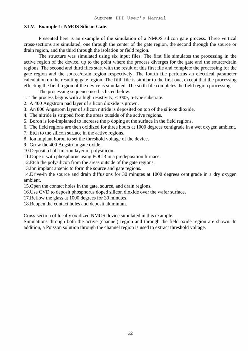
Suprem-III User's Manual
62
XLV. Example 1: NMOS Silicon Gate.
Presented here is an example of the simulation of a NMOS silicon gate process. Three verticalcross-sections are simulated, one through the center of the gate region, the second through the source ordrain region, and the third through the isolation or field region.
The structure was simulated using six input files. The first file simulates the processing in theactive region of the device, up to the point where the process diverges for the gate and the source/drainregions. The second and third files start with the result of this first file and complete the processing for thegate region and the source/drain region respectively. The fourth file performs an electrical parametercalculation on the resulting gate region. The fifth file is similar to the first one, except that the processingeffecting the field region of the device is simulated. The sixth file completes the field region processing.
The processing sequence used is listed below.1. The process begins with a high resistivity, <100>, p-type substrate.2. A 400 Angstrom pad layer of silicon dioxide is grown.3. An 800 Angstrom layer of silicon nitride is deposited on top of the silicon dioxide.4. The nitride is stripped from the areas outside of the active regions.5. Boron is ion-implanted to increase the p doping at the surface in the field regions.6. The field regions are then oxidized for three hours at 1000 degrees centigrade in a wet oxygen ambient.7. Etch to the silicon surface in the active regions.8. Ion implant boron to set the threshold voltage of the device.9. Grow the 400 Angstrom gate oxide.10. Deposit a half micron layer of polysilicon.11. Dope it with phosphorus using POCl3 in a predeposition furnace.12. Etch the polysilicon from the areas outside of the gate regions.13. Ion implant arsenic to form the source and gate regions.14. Drive-in the source and drain diffusions for 30 minutes at 1000 degrees centigrade in a dry oxygenambient.15. Open the contact holes in the gate, source, and drain regions.16. Use CVD to deposit phosphorus doped silicon dioxide over the wafer surface.17. Reflow the glass at 1000 degrees for 30 minutes.18. Reopen the contact holes and deposit aluminum.
Cross-section of locally oxidized NMOS device simulated in this example.Simulations through both the active (channel) region and through the field oxide region are shown. Inaddition, a Poisson solution through the channel region is used to extract threshold voltage.
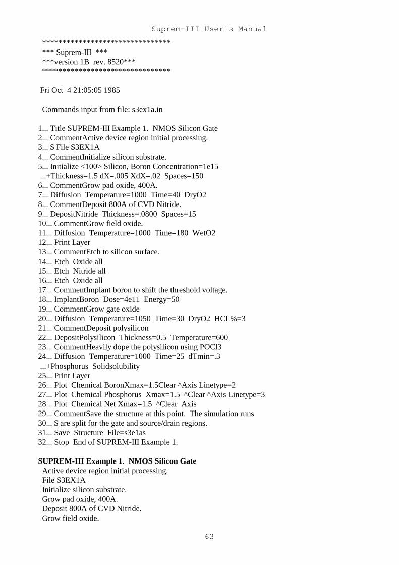
Suprem-III User's Manual
63
******************************** *** Suprem-III *** ***version 1B rev. 8520*** ********************************
Fri Oct 4 21:05:05 1985
Commands input from file: s3ex1a.in
1... Title SUPREM-III Example 1. NMOS Silicon Gate2... CommentActive device region initial processing.3... $ File S3EX1A4... CommentInitialize silicon substrate.5... Initialize <100> Silicon, Boron Concentration=1e15 ...+Thickness=1.5 dX=.005 XdX=.02 Spaces=1506... CommentGrow pad oxide, 400A.7... Diffusion Temperature=1000 Time=40 DryO28... CommentDeposit 800A of CVD Nitride.9... DepositNitride Thickness=.0800 Spaces=1510... CommentGrow field oxide.11... Diffusion Temperature=1000 Time=180 WetO212... Print Layer13... CommentEtch to silicon surface.14... Etch Oxide all15... Etch Nitride all16... Etch Oxide all17... CommentImplant boron to shift the threshold voltage.18... ImplantBoron Dose=4e11 Energy=5019... CommentGrow gate oxide20... Diffusion Temperature=1050 Time=30 DryO2 HCL%=321... CommentDeposit polysilicon22... DepositPolysilicon Thickness=0.5 Temperature=60023... CommentHeavily dope the polysilicon using POCl324... Diffusion Temperature=1000 Time=25 dTmin=.3 ...+Phosphorus Solidsolubility25... Print Layer26... Plot Chemical BoronXmax=1.5Clear ^Axis Linetype=227... Plot Chemical Phosphorus Xmax=1.5 ^Clear ^Axis Linetype=328... Plot Chemical Net Xmax=1.5 ^Clear Axis29... CommentSave the structure at this point. The simulation runs30... $ are split for the gate and source/drain regions.31... Save Structure File=s3e1as32... Stop End of SUPREM-III Example 1.
SUPREM-III Example 1. NMOS Silicon Gate Active device region initial processing. File S3EX1A Initialize silicon substrate. Grow pad oxide, 400A. Deposit 800A of CVD Nitride. Grow field oxide.
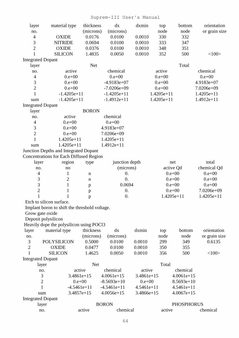
Suprem-III User's Manual
64
layer material type thickness dx dxmin top bottom orientationno. (microns) (microns) node node or grain size4 OXIDE 0.0176 0.0100 0.0010 330 3323 NITRIDE 0.0694 0.0100 0.0010 333 3472 OXIDE 0.0376 0.0100 0.0010 348 3511 SILICON 1.4835 0.0050 0.0010 352 500 <100>
Integrated Dopantlayer Net Totalno. active chemical active chemical4 0.e+00 0.e+00 0.e+00 0.e+003 0.e+00 -4.9183e+07 0.e+00 4.9183e+072 0.e+00 -7.0206e+09 0.e+00 7.0206e+091 -1.4205e+11 -1.4205e+11 1.4205e+11 1.4205e+11
sum -1.4205e+11 -1.4912e+11 1.4205e+11 1.4912e+11Integrated Dopant
layer BORONno. active chemical4 0.e+00 0.e+003 0.e+00 4.9183e+072 0.e+00 7.0206e+091 1.4205e+11 1.4205e+11
sum 1.4205e+11 1.4912e+11Junction Depths and Integrated DopantConcentrations for Each Diffused Region
layer region type junction depth net totalno. no (microns) active Qd chemical Qd4 1 n 0. 0.e+00 0.e+003 2 n 0. 0.e+00 0.e+003 1 p 0.0694 0.e+00 0.e+002 1 p 0. 0.e+00 7.0206e+091 1 p 0. 1.4205e+11 1.4205e+11
Etch to silicon surface. Implant boron to shift the threshold voltage. Grow gate oxide Deposit polysilicon Heavily dope the polysilicon using POCl3layer material type thickness dx dxmin top bottom orientationno. (microns) (microns) node node or grain size3 POLYSILICON 0.5000 0.0100 0.0010 299 349 0.61352 OXIDE 0.0477 0.0100 0.0010 350 3551 SILICON 1.4625 0.0050 0.0010 356 500 <100>
Integrated Dopantlayer Net Totalno. active chemical active chemical3 3.4861e+15 4.0061e+15 3.4861e+15 4.0061e+152 0.e+00 -8.5693e+10 0.e+00 8.5693e+101 -4.5461e+11 -4.5461e+11 4.5461e+11 4.5461e+11
sum 3.4857e+15 4.0056e+15 3.4866e+15 4.0067e+15Integrated Dopant
layer BORON PHOSPHORUSno. active chemical active chemical
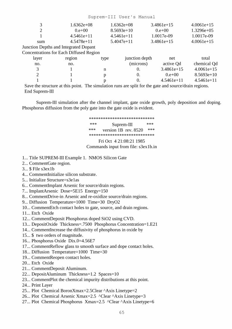
Suprem-III User's Manual
65
3 1.6362e+08 1.6362e+08 3.4861e+15 4.0061e+152 0.e+00 8.5693e+10 0.e+00 1.3296e+051 4.5461e+11 4.5461e+11 1.0017e-09 1.0017e-09
sum 4.5478e+11 5.4047e+11 3.4861e+15 4.0061e+15Junction Depths and Integrated DopantConcentrations for Each Diffused Region
layer region type junction depth net totalno. no. (microns) active Qd chemical Qd3 1 n 0. 3.4861e+15 4.0061e+152 1 p 0. 0.e+00 8.5693e+101 1 p 0. 4.5461e+11 4.5461e+11
Save the structure at this point. The simulation runs are split for the gate and source/drain regions. End Suprem-III
Suprem-III simulation after the channel implant, gate oxide growth, poly deposition and doping.Phosphorus diffusion from the poly gate into the gate oxide is evident.
******************************* Suprem-III ****** version 1B rev. 8520 *******************************
Fri Oct 4 21:08:21 1985Commands input from file: s3ex1b.in
1... Title SUPREM-III Example 1. NMOS Silicon Gate2... CommentGate region.3... $ File s3ex1b4... CommentInitialize silicon substrate.5... Initialize Structure=s3e1as6... CommentImplant Arsenic for source/drain regions.7... ImplantArsenic Dose=5E15 Energy=1508... CommentDrive-in Arsenic and re-oxidize source/drain regions.9... Diffusion Temperature=1000 Time=30 DryO210... CommentEtch contact holes to gate, source, and drain regions.11... Etch Oxide12... CommentDeposit Phosphorus doped SiO2 using CVD.13... DepositOxide Thickness=.7500 Phosphorus Concentration=1.E2114... CommentIncrease the diffusivity of phosphorus in oxide by15... $ two orders of magnitude.16... Phosphorus Oxide Dix.0=4.56E717... CommentReflow glass to smooth surface and dope contact holes.18... Diffusion Temperature=1000 Time=3019... CommentReopen contact holes.20... Etch Oxide21... CommentDeposit Aluminum.22... DepositAluminum Thickness=1.2 Spaces=1023... CommentPlot the chemical impurity distributions at this point.24... Print Layer25... Plot Chemical BoronXmax=2.5Clear ^Axis Linetype=226... Plot Chemical Arsenic Xmax=2.5 ^Clear ^Axis Linetype=327... Plot Chemical Phosphorus Xmax=2.5 ^Clear ^Axis Linetype=6
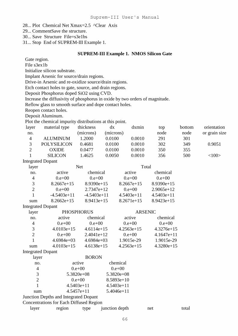
Suprem-III User's Manual
66
28... Plot Chemical Net Xmax=2.5 ^Clear Axis29... CommentSave the structure.30... Save Structure File=s3e1bs31... Stop End of SUPREM-III Example 1.
SUPREM-III Example 1. NMOS Silicon Gate Gate region. File s3ex1b Initialize silicon substrate. Implant Arsenic for source/drain regions. Drive-in Arsenic and re-oxidize source/drain regions. Etch contact holes to gate, source, and drain regions. Deposit Phosphorus doped SiO2 using CVD. Increase the diffusivity of phosphorus in oxide by two orders of magnitude. Reflow glass to smooth surface and dope contact holes. Reopen contact holes. Deposit Aluminum. Plot the chemical impurity distributions at this point.
layer material type thickness dx dxmin top bottom orientationno. (microns) (microns) node node or grain size4 ALUMINUM 1.2000 0.0100 0.0010 291 3013 POLYSILICON 0.4681 0.0100 0.0010 302 349 0.90512 OXIDE 0.0477 0.0100 0.0010 350 3551 SILICON 1.4625 0.0050 0.0010 356 500 <100>
Integrated Dopantlayer Net Totalno. active chemical active chemical4 0.e+00 0.e+00 0.e+00 0.e+003 8.2667e+15 8.9390e+15 8.2667e+15 8.9390e+152 0.e+00 2.7347e+12 0.e+00 2.9065e+121 -4.5403e+11 -4.5403e+11 4.5403e+11 4.5403e+11
sum 8.2662e+15 8.9413e+15 8.2671e+15 8.9423e+15Integrated Dopant
layer PHOSPHORUS ARSENICno. active chemical active chemical4 0.e+00 0.e+00 0.e+00 0.e+003 4.0103e+15 4.6114e+15 4.2563e+15 4.3276e+152 0.e+00 2.4041e+12 0.e+00 4.1647e+111 4.6984e+03 4.6984e+03 1.9015e-29 1.9015e-29
sum 4.0103e+15 4.6138e+15 4.2563e+15 4.3280e+15Integrated Dopant
layer BORONno. active chemical4 0.e+00 0.e+003 5.3820e+08 5.3820e+082 0.e+00 8.5893e+101 4.5403e+11 4.5403e+11
sum 4.5457e+11 5.4046e+11Junction Depths and Integrated DopantConcentrations for Each Diffused Region
layer region type junction depth net total
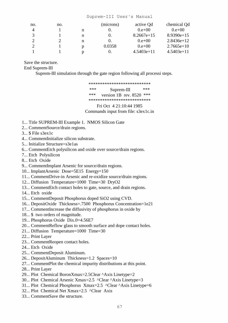
Suprem-III User's Manual
67
no. no. (microns) active Qd chemical Qd4 1 n 0. 0.e+00 0.e+003 1 n 0. 8.2667e+15 8.9390e+152 2 n 0. 0.e+00 2.8436e+122 1 p 0.0358 0.e+00 2.7665e+101 1 p 0. 4.5403e+11 4.5403e+11
Save the structure. End Suprem-III
Suprem-III simulation through the gate region following all processi steps.
****************************** Suprem-III ****** version 1B rev. 8520 ******************************
Fri Oct 4 21:10:44 1985Commands input from file: s3ex1c.in
1... Title SUPREM-III Example 1. NMOS Silicon Gate2... CommentSource/drain regions.3... $ File s3ex1c4... CommentInitialize silicon substrate.5... Initialize Structure=s3e1as6... CommentEtch polysilicon and oxide over source/drain regions.7... Etch Polysilicon8... Etch Oxide9... CommentImplant Arsenic for source/drain regions.10... ImplantArsenic Dose=5E15 Energy=15011... CommentDrive-in Arsenic and re-oxidize source/drain regions.12... Diffusion Temperature=1000 Time=30 DryO213... CommentEtch contact holes to gate, source, and drain regions.14... Etch oxide15... CommentDeposit Phosphorus doped SiO2 using CVD.16... DepositOxide Thickness=.7500 Phosphorus Concentration=1e2117... CommentIncrease the diffusivity of phosphorus in oxide by18... $ two orders of magnitude.19... Phosphorus Oxide Dix.0=4.56E720... CommentReflow glass to smooth surface and dope contact holes.21... Diffusion Temperature=1000 Time=3022... Print Layer23... CommentReopen contact holes.24... Etch Oxide25... CommentDeposit Aluminum.26... DepositAluminum Thickness=1.2 Spaces=1027... CommentPlot the chemical impurity distributions at this point.28... Print Layer29... Plot Chemical BoronXmax=2.5Clear ^Axis Linetype=230... Plot Chemical Arsenic Xmax=2.5 ^Clear ^Axis Linetype=331... Plot Chemical Phosphorus Xmax=2.5 ^Clear ^Axis Linetype=632... Plot Chemical Net Xmax=2.5 ^Clear Axis33... CommentSave the structure.

Suprem-III User's Manual
68
34... Save Structure File=s3e1cs35... Stop End of SUPREM-III Example 1.
SUPREM-III Example 1. NMOS Silicon Gate Source/drain regions. File s3ex1c Initialize silicon substrate. Etch polysilicon and oxide over source/drain regions. Implant Arsenic for source/drain regions. Drive-in Arsenic and re-oxidize source/drain regions. Error number 204 detected in line number 12 During this step,14 intermediate solutions resulted in distributions with at least one negative concentration. Etch contact holes to gate, source, and drain regions. Deposit Phosphorus doped SiO2 using CVD. Increase the diffusivity of phosphorus in oxide by two orders of magnitude. Reflow glass to smooth surface and dope contact holes.layer material type thickness dx dxmin top bottom orientationno. (microns) (microns) node node or grain size2 OXIDE 0.7500 0.0100 0.0010 285 3601 SILICON 1.4367 0.0050 0.0010 361 500 <100>
Integrated Dopantlayer Net Totalno. active chemical active chemical2 0.e+00 7.3656e+16 0.e+00 7.3656e+161 5.2811e+15 5.5049e+15 5.2818e+15 5.5056e+15
sum 5.2811e+15 7.9161e+16 5.2818e+15 7.9161e+16Integrated Dopantlayer PHOSPHORUS ARSENICno. active chemical active chemical2 0.e+00 7.3652e+16 0.e+00 3.4378e+121 6.6798e+14 6.7348e+14 4.6135e+15 4.8317e+15
sum 6.6798e+14 7.4326e+16 4.6135e+15 4.8352e+15Integrated Dopantlayer BORONno. active chemical2 0.e+00 1.0536e+101 3.5397e+11 3.5397e+11
sum 3.5397e+11 3.6451e+11Junction Depths and Integrated DopantConcentrations for Each Diffused Regionlayer region type junction depth net totalno. no. (microns) active Qd chemical Qd2 1 n 0. 0.e+00 7.3656e+161 2 n 0. 5.2812e+15 5.5054e+151 1 p 0.5219 1.3184e+11 1.3691e+11
Deposit Aluminum. Plot the chemical impurity distributions at this point.layer material type thickness dx dxmin top bottom orientationno. (microns) (microns) node node or grain size
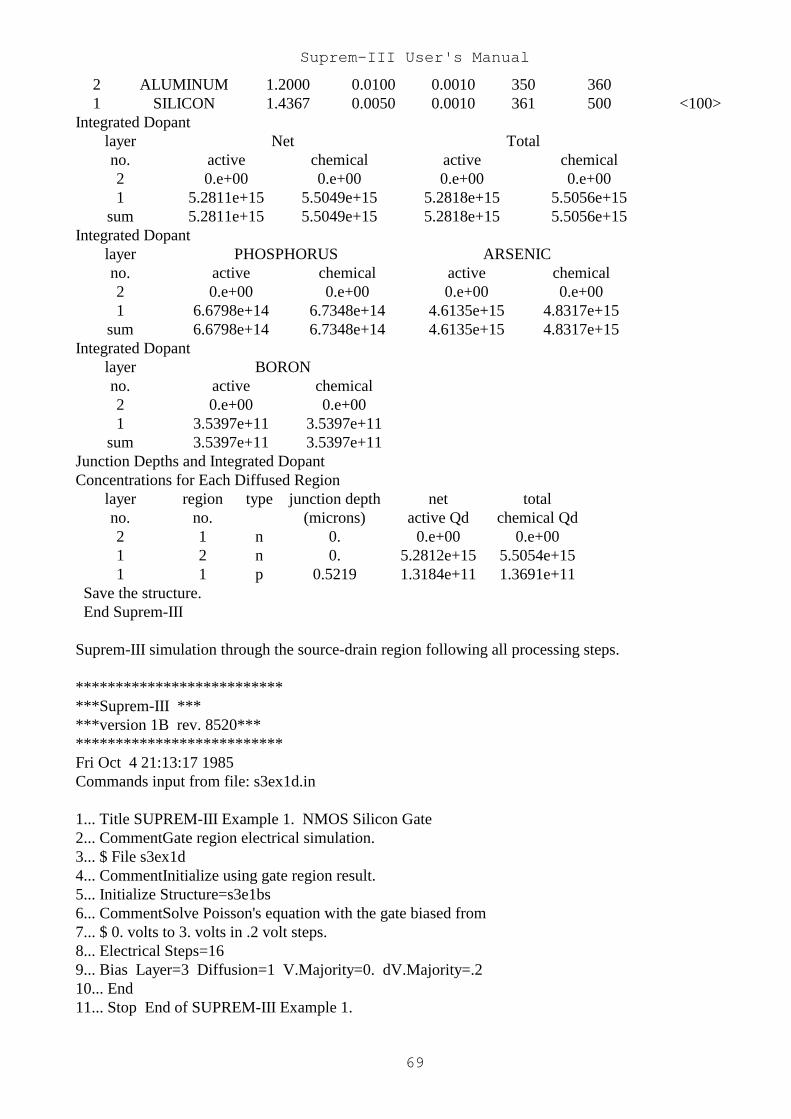
Suprem-III User's Manual
69
2 ALUMINUM 1.2000 0.0100 0.0010 350 3601 SILICON 1.4367 0.0050 0.0010 361 500 <100>
Integrated Dopantlayer Net Totalno. active chemical active chemical2 0.e+00 0.e+00 0.e+00 0.e+001 5.2811e+15 5.5049e+15 5.2818e+15 5.5056e+15
sum 5.2811e+15 5.5049e+15 5.2818e+15 5.5056e+15Integrated Dopant
layer PHOSPHORUS ARSENICno. active chemical active chemical2 0.e+00 0.e+00 0.e+00 0.e+001 6.6798e+14 6.7348e+14 4.6135e+15 4.8317e+15
sum 6.6798e+14 6.7348e+14 4.6135e+15 4.8317e+15Integrated Dopant
layer BORONno. active chemical2 0.e+00 0.e+001 3.5397e+11 3.5397e+11
sum 3.5397e+11 3.5397e+11Junction Depths and Integrated DopantConcentrations for Each Diffused Region
layer region type junction depth net totalno. no. (microns) active Qd chemical Qd2 1 n 0. 0.e+00 0.e+001 2 n 0. 5.2812e+15 5.5054e+151 1 p 0.5219 1.3184e+11 1.3691e+11
Save the structure. End Suprem-III
Suprem-III simulation through the source-drain region following all processing steps.
*****************************Suprem-III ******version 1B rev. 8520*****************************Fri Oct 4 21:13:17 1985Commands input from file: s3ex1d.in
1... Title SUPREM-III Example 1. NMOS Silicon Gate2... CommentGate region electrical simulation.3... $ File s3ex1d4... CommentInitialize using gate region result.5... Initialize Structure=s3e1bs6... CommentSolve Poisson's equation with the gate biased from7... $ 0. volts to 3. volts in .2 volt steps.8... Electrical Steps=169... Bias Layer=3 Diffusion=1 V.Majority=0. dV.Majority=.210... End11... Stop End of SUPREM-III Example 1.
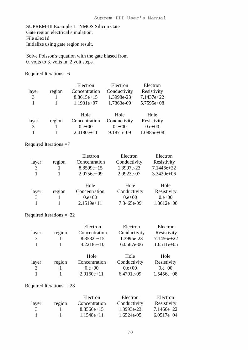
Suprem-III User's Manual
70
SUPREM-III Example 1. NMOS Silicon Gate Gate region electrical simulation. File s3ex1d Initialize using gate region result.
Solve Poisson's equation with the gate biased from 0. volts to 3. volts in .2 volt steps.
Required Iterations =6
Electron Electron Electronlayer region Concentration Conductivity Resistivity
3 1 8.8615e+15 1.3998e-23 7.1437e+221 1 1.1931e+07 1.7363e-09 5.7595e+08
Hole Hole Holelayer region Concentration Conductivity Resistivity
3 1 0.e+00 0.e+00 0.e+001 1 2.4180e+11 9.1871e-09 1.0885e+08
Required Iterations =7
Electron Electron Electronlayer region Concentration Conductivity Resistivity
3 1 8.8599e+15 1.3997e-23 7.1446e+221 1 2.0756e+09 2.9923e-07 3.3420e+06
Hole Hole Holelayer region Concentration Conductivity Resistivity
3 1 0.e+00 0.e+00 0.e+001 1 2.1519e+11 7.3465e-09 1.3612e+08
Required Iterations = 22
Electron Electron Electronlayer region Concentration Conductivity Resistivity
3 1 8.8582e+15 1.3995e-23 7.1456e+221 1 4.2218e+10 6.0567e-06 1.6511e+05
Hole Hole Holelayer region Concentration Conductivity Resistivity
3 1 0.e+00 0.e+00 0.e+001 1 2.0160e+11 6.4701e-09 1.5456e+08
Required Iterations = 23
Electron Electron Electronlayer region Concentration Conductivity Resistivity
3 1 8.8566e+15 1.3993e-23 7.1466e+221 1 1.1548e+11 1.6524e-05 6.0517e+04
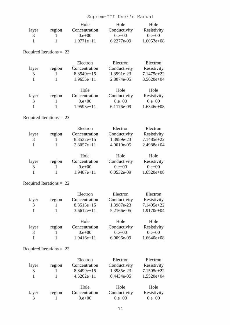
Suprem-III User's Manual
71
Hole Hole Holelayer region Concentration Conductivity Resistivity
3 1 0.e+00 0.e+00 0.e+001 1 1.9771e+11 6.2277e-09 1.6057e+08
Required Iterations = 23
Electron Electron Electronlayer region Concentration Conductivity Resistivity
3 1 8.8549e+15 1.3991e-23 7.1475e+221 1 1.9655e+11 2.8074e-05 3.5620e+04
Hole Hole Holelayer region Concentration Conductivity Resistivity
3 1 0.e+00 0.e+00 0.e+001 1 1.9593e+11 6.1176e-09 1.6346e+08
Required Iterations = 23
Electron Electron Electronlayer region Concentration Conductivity Resistivity
3 1 8.8532e+15 1.3989e-23 7.1485e+221 1 2.8057e+11 4.0019e-05 2.4988e+04
Hole Hole Holelayer region Concentration Conductivity Resistivity
3 1 0.e+00 0.e+00 0.e+001 1 1.9487e+11 6.0532e-09 1.6520e+08
Required Iterations = 22
Electron Electron Electronlayer region Concentration Conductivity Resistivity
3 1 8.8515e+15 1.3987e-23 7.1495e+221 1 3.6612e+11 5.2166e-05 1.9170e+04
Hole Hole Holelayer region Concentration Conductivity Resistivity
3 1 0.e+00 0.e+00 0.e+001 1 1.9416e+11 6.0096e-09 1.6640e+08
Required Iterations = 22
Electron Electron Electronlayer region Concentration Conductivity Resistivity
3 1 8.8499e+15 1.3985e-23 7.1505e+221 1 4.5262e+11 6.4434e-05 1.5520e+04
Hole Hole Holelayer region Concentration Conductivity Resistivity
3 1 0.e+00 0.e+00 0.e+00
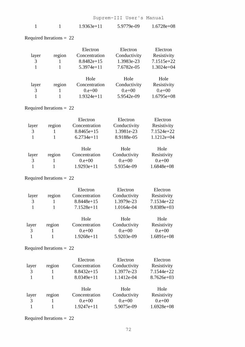
Suprem-III User's Manual
72
1 1 1.9363e+11 5.9779e-09 1.6728e+08
Required Iterations = 22
Electron Electron Electronlayer region Concentration Conductivity Resistivity
3 1 8.8482e+15 1.3983e-23 7.1515e+221 1 5.3974e+11 7.6782e-05 1.3024e+04
Hole Hole Holelayer region Concentration Conductivity Resistivity
3 1 0.e+00 0.e+00 0.e+001 1 1.9324e+11 5.9542e-09 1.6795e+08
Required Iterations = 22
Electron Electron Electronlayer region Concentration Conductivity Resistivity
3 1 8.8465e+15 1.3981e-23 7.1524e+221 1 6.2734e+11 8.9188e-05 1.1212e+04
Hole Hole Holelayer region Concentration Conductivity Resistivity
3 1 0.e+00 0.e+00 0.e+001 1 1.9293e+11 5.9354e-09 1.6848e+08
Required Iterations = 22
Electron Electron Electronlayer region Concentration Conductivity Resistivity
3 1 8.8448e+15 1.3979e-23 7.1534e+221 1 7.1528e+11 1.0164e-04 9.8389e+03
Hole Hole Holelayer region Concentration Conductivity Resistivity
3 1 0.e+00 0.e+00 0.e+001 1 1.9268e+11 5.9203e-09 1.6891e+08
Required Iterations = 22
Electron Electron Electronlayer region Concentration Conductivity Resistivity
3 1 8.8432e+15 1.3977e-23 7.1544e+221 1 8.0349e+11 1.1412e-04 8.7626e+03
Hole Hole Holelayer region Concentration Conductivity Resistivity
3 1 0.e+00 0.e+00 0.e+001 1 1.9247e+11 5.9075e-09 1.6928e+08
Required Iterations = 22
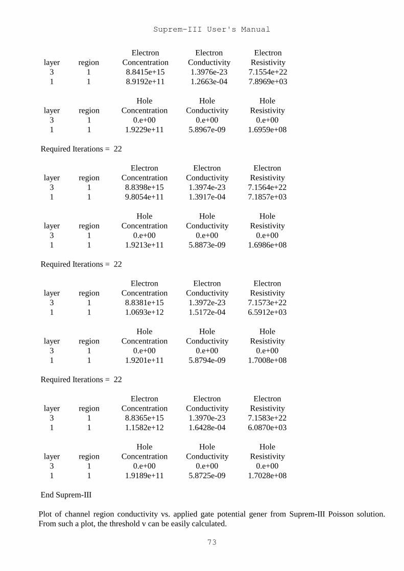
Suprem-III User's Manual
73
Electron Electron Electronlayer region Concentration Conductivity Resistivity
3 1 8.8415e+15 1.3976e-23 7.1554e+221 1 8.9192e+11 1.2663e-04 7.8969e+03
Hole Hole Holelayer region Concentration Conductivity Resistivity
3 1 0.e+00 0.e+00 0.e+001 1 1.9229e+11 5.8967e-09 1.6959e+08
Required Iterations = 22
Electron Electron Electronlayer region Concentration Conductivity Resistivity
3 1 8.8398e+15 1.3974e-23 7.1564e+221 1 9.8054e+11 1.3917e-04 7.1857e+03
Hole Hole Holelayer region Concentration Conductivity Resistivity
3 1 0.e+00 0.e+00 0.e+001 1 1.9213e+11 5.8873e-09 1.6986e+08
Required Iterations = 22
Electron Electron Electronlayer region Concentration Conductivity Resistivity
3 1 8.8381e+15 1.3972e-23 7.1573e+221 1 1.0693e+12 1.5172e-04 6.5912e+03
Hole Hole Holelayer region Concentration Conductivity Resistivity
3 1 0.e+00 0.e+00 0.e+001 1 1.9201e+11 5.8794e-09 1.7008e+08
Required Iterations = 22
Electron Electron Electronlayer region Concentration Conductivity Resistivity
3 1 8.8365e+15 1.3970e-23 7.1583e+221 1 1.1582e+12 1.6428e-04 6.0870e+03
Hole Hole Holelayer region Concentration Conductivity Resistivity
3 1 0.e+00 0.e+00 0.e+001 1 1.9189e+11 5.8725e-09 1.7028e+08
End Suprem-III
Plot of channel region conductivity vs. applied gate potential gener from Suprem-III Poisson solution.From such a plot, the threshold v can be easily calculated.

Suprem-III User's Manual
74

Suprem-III User's Manual
75
************************** *** Suprem-III*** ***version 1B rev. 8520*** **************************
Fri Oct 4 21:14:31 1985
Commands input from file: s3ex1e.in
1... Title SUPREM-III Example 1. NMOS Silicon Gate2... CommentIsolation region initial processing.3... $ File s3ex1e4... CommentInitialize silicon substrate.5... Initialize <100> Silicon, Boron Concentration=1e15 ... +Thickness=3.0 dX=.01 Spaces=1506... CommentGrow pad oxide, 400A.7... Diffusion Temperature=1000 Time=40 DryO28... CommentImplant boron to increase field region doping.9... ImplantBoron dose=1e13 energy=15010... CommentGrow field oxide.11... Diffusion Temperature=1000 Time=180 WetO212... Print Layer13... CommentImplant boron to shift the enhancement threshold voltage14... ImplantBoron Dose=4e11 Energy=5015... CommentGrow gate oxide16... Diffusion Temperature=1050 Time=30 DryO2 HCL%=317... CommentDeposit polysilicon18... DepositPolysilicon Thickness=0.5 Temperature=60019... CommentHeavily dope the polysilicon using POCl320... Diffusion Temperature=1000 Time=25 dTmin=.3 ...+Phosphorus Solidsolubility21... Print Layer22... Plot Chemical BoronClear ^Axis Linetype=223... Plot Chemical Phosphorus ^Clear ^Axis Linetype=324... Plot Chemical Net ^Clear Axis25... CommentSave the structure at this point.26... Save Structure File=s3e1es27... Stop End of SUPREM-III Example 1.
SUPREM-III Example 1. NMOS Silicon Gate Isolation region initial processing. File s3ex1e Initialize silicon substrate. Grow pad oxide, 400A. Implant boron to increase field region doping. Grow field oxide.
layer material type thickness dx dxmin top bottom orientationno. (microns) (microns) node node or grain size2 OXIDE 0.7610 0.0100 0.0010 348 3741 SILICON 2.6652 0.0100 0.0010 375 500 <100>

Suprem-III User's Manual
76
Integrated Dopantlayer Net Totalno. active chemical active chemical2 0.e+00 -6.1515e+12 0.e+00 6.1515e+121 -4.1597e+12 -4.1597e+12 4.1597e+12 4.1597e+12
sum -4.1597e+12 -1.0311e+13 4.1597e+12 1.0311e+13
Integrated Dopantlayer BORONno. active chemical2 0.e+00 6.1515e+121 4.1597e+12 4.1597e+12
sum 4.1597e+12 1.0311e+13
Junction Depths and Integrated DopantConcentrations for Each Diffused Region
layer region type junction depth net totalno. no. (microns) active Qd chemical Qd2 1 p 0. 0.e+00 6.1515e+121 1 p 0. 4.1597e+12 4.1597e+12
Implant boron to shift the enhancement threshold voltage. Grow gate oxide Deposit polysilicon Heavily dope the polysilicon using POCl3layer material type thickness dx dxmin top bottom orientationno. (microns) (microns) node node or grain size3 POLYSILICON 0.5000 0.0100 0.0010 297 347 0.61352 OXIDE 0.7657 0.0100 0.0010 348 3741 SILICON 2.6631 0.0100 0.0010 375 500 <100>
Integrated Dopantlayer Net Totalno. active chemical active chemical3 3.4861e+15 4.0061e+15 3.4861e+15 4.0061e+152 0.e+00 -6.6459e+12 0.e+00 6.6459e+121 -4.0648e+12 -4.0648e+12 4.0648e+12 4.0648e+12
sum 3.4821e+15 3.9954e+15 3.4902e+15 4.0168e+15
Integrated Dopantlayer BORON PHOSPHORUSno. active chemical active chemical3 1.2079e+07 1.2079e+07 3.4861e+15 4.0061e+152 0.e+00 6.6459e+12 0.e+00 6.2621e+051 4.0648e+12 4.0648e+12 0.e+00 0.e+00
sum 4.0649e+12 1.0711e+13 3.4861e+15 4.0061e+15
Junction Depths and Integrated DopantConcentrations for Each Diffused Region
layer region type junction depth net total
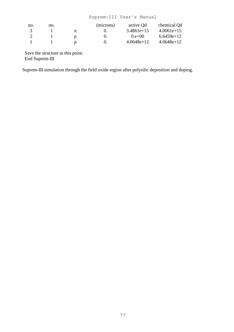
Suprem-III User's Manual
77
no. no. (microns) active Qd chemical Qd3 1 n 0. 3.4861e+15 4.0061e+152 1 p 0. 0.e+00 6.6459e+121 1 p 0. 4.0648e+12 4.0648e+12
Save the structure at this point. End Suprem-III
Suprem-III simulation through the field oxide region after polysilic deposition and doping.
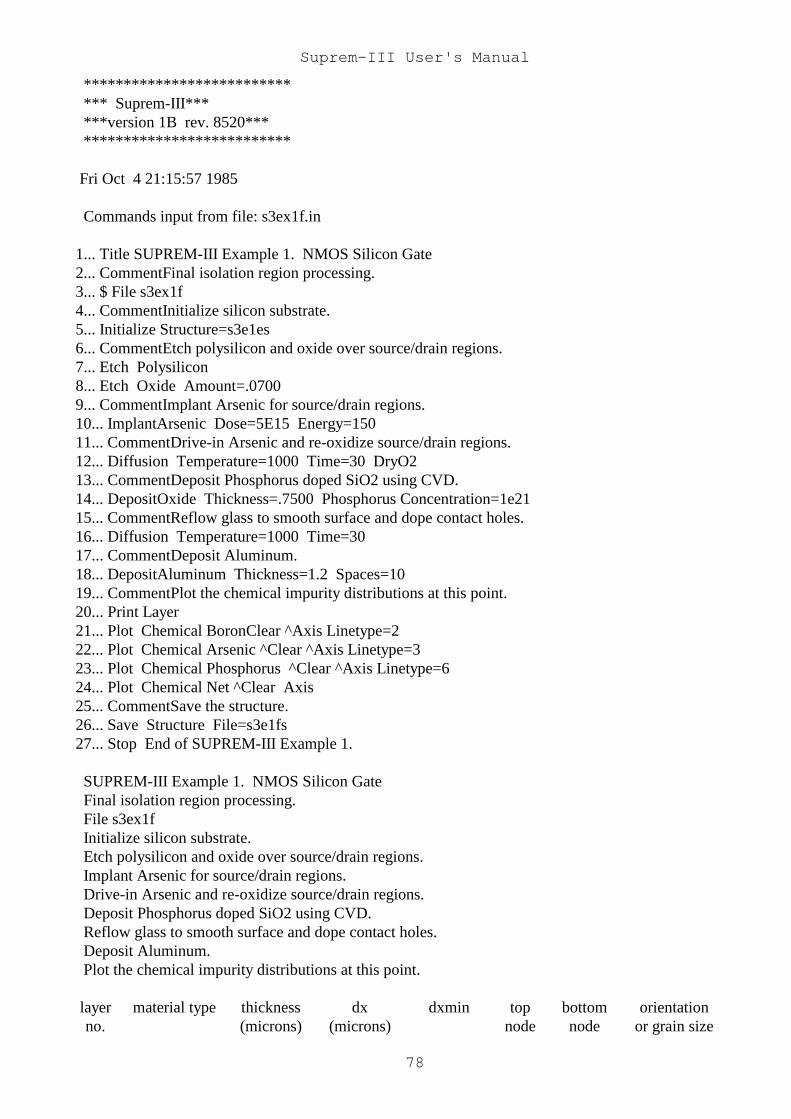
Suprem-III User's Manual
78
************************** *** Suprem-III*** ***version 1B rev. 8520*** **************************
Fri Oct 4 21:15:57 1985
Commands input from file: s3ex1f.in
1... Title SUPREM-III Example 1. NMOS Silicon Gate2... CommentFinal isolation region processing.3... $ File s3ex1f4... CommentInitialize silicon substrate.5... Initialize Structure=s3e1es6... CommentEtch polysilicon and oxide over source/drain regions.7... Etch Polysilicon8... Etch Oxide Amount=.07009... CommentImplant Arsenic for source/drain regions.10... ImplantArsenic Dose=5E15 Energy=15011... CommentDrive-in Arsenic and re-oxidize source/drain regions.12... Diffusion Temperature=1000 Time=30 DryO213... CommentDeposit Phosphorus doped SiO2 using CVD.14... DepositOxide Thickness=.7500 Phosphorus Concentration=1e2115... CommentReflow glass to smooth surface and dope contact holes.16... Diffusion Temperature=1000 Time=3017... CommentDeposit Aluminum.18... DepositAluminum Thickness=1.2 Spaces=1019... CommentPlot the chemical impurity distributions at this point.20... Print Layer21... Plot Chemical BoronClear ^Axis Linetype=222... Plot Chemical Arsenic ^Clear ^Axis Linetype=323... Plot Chemical Phosphorus ^Clear ^Axis Linetype=624... Plot Chemical Net ^Clear Axis25... CommentSave the structure.26... Save Structure File=s3e1fs27... Stop End of SUPREM-III Example 1.
SUPREM-III Example 1. NMOS Silicon Gate Final isolation region processing. File s3ex1f Initialize silicon substrate. Etch polysilicon and oxide over source/drain regions. Implant Arsenic for source/drain regions. Drive-in Arsenic and re-oxidize source/drain regions. Deposit Phosphorus doped SiO2 using CVD. Reflow glass to smooth surface and dope contact holes. Deposit Aluminum. Plot the chemical impurity distributions at this point.
layer material type thickness dx dxmin top bottom orientationno. (microns) (microns) node node or grain size
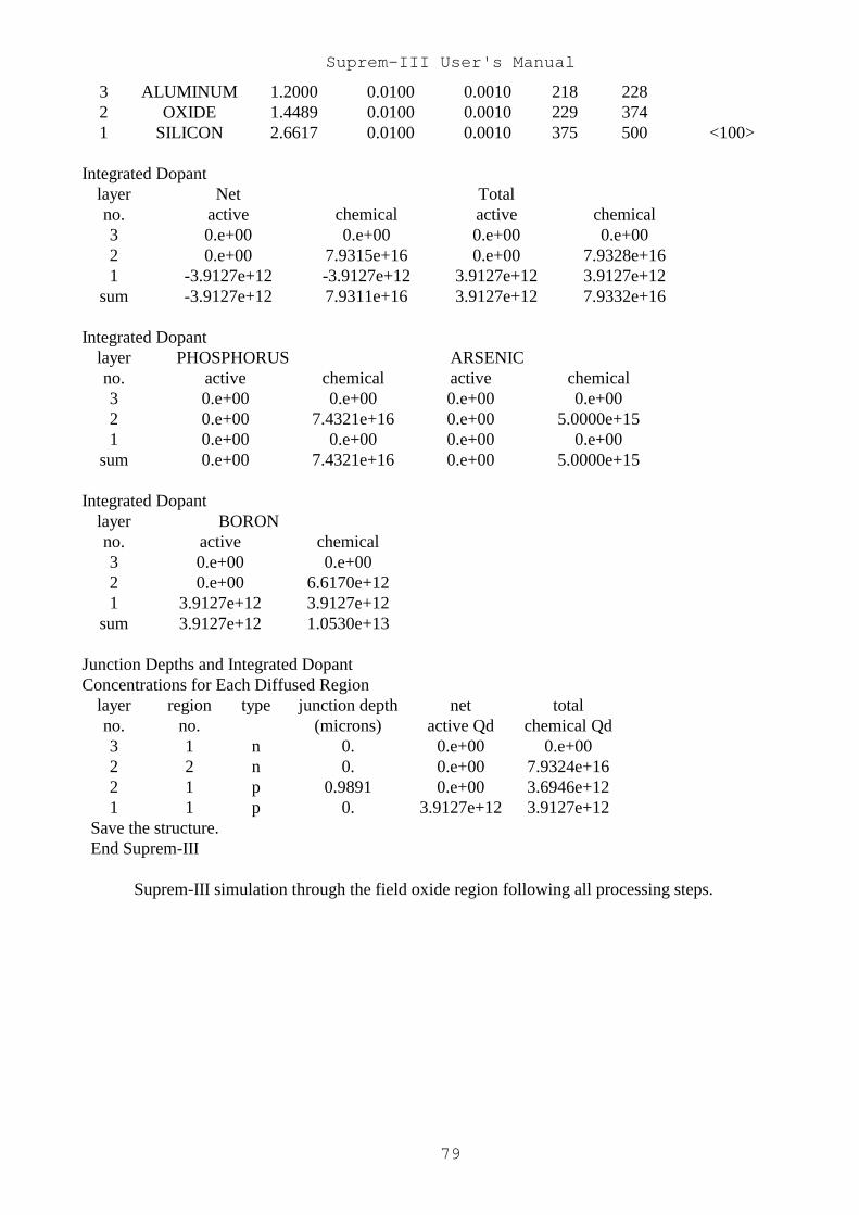
Suprem-III User's Manual
79
3 ALUMINUM 1.2000 0.0100 0.0010 218 2282 OXIDE 1.4489 0.0100 0.0010 229 3741 SILICON 2.6617 0.0100 0.0010 375 500 <100>
Integrated Dopantlayer Net Totalno. active chemical active chemical3 0.e+00 0.e+00 0.e+00 0.e+002 0.e+00 7.9315e+16 0.e+00 7.9328e+161 -3.9127e+12 -3.9127e+12 3.9127e+12 3.9127e+12
sum -3.9127e+12 7.9311e+16 3.9127e+12 7.9332e+16
Integrated Dopantlayer PHOSPHORUS ARSENICno. active chemical active chemical3 0.e+00 0.e+00 0.e+00 0.e+002 0.e+00 7.4321e+16 0.e+00 5.0000e+151 0.e+00 0.e+00 0.e+00 0.e+00
sum 0.e+00 7.4321e+16 0.e+00 5.0000e+15
Integrated Dopantlayer BORONno. active chemical3 0.e+00 0.e+002 0.e+00 6.6170e+121 3.9127e+12 3.9127e+12
sum 3.9127e+12 1.0530e+13
Junction Depths and Integrated DopantConcentrations for Each Diffused Region
layer region type junction depth net totalno. no. (microns) active Qd chemical Qd3 1 n 0. 0.e+00 0.e+002 2 n 0. 0.e+00 7.9324e+162 1 p 0.9891 0.e+00 3.6946e+121 1 p 0. 3.9127e+12 3.9127e+12
Save the structure. End Suprem-III
Suprem-III simulation through the field oxide region following all processing steps.
Suprem-III User's Manual
80
XLVI. Example 2: Bipolar Polysilicon Doped Emitter.
Presented here is an example of the simulation of a bipolar process with a polysilicon dopedemitter. Two vertical cross-sections are simulated, one through the emitter region, and other through theisolation region.
The structure was simulated using five input files. The first file simulates the processing in theactive region of the device up to the point of the isolation oxidation. The second file starts with the resultof this first file and completes the processing in the active region. The third file performs an electricalparameter calculation on the resulting structure. As in the first example, the fourth file is similar to thefirst one, except that the processing in the isolation region is simulated. The fifth file completes theisolation region processing.
The processing sequence used is listed below.
1. The process begins with a high resistivity, <100>, p-type substrate.2. Thermally oxidize the substrate, growing approximately one micron of silicon dioxide.3. Remove the oxide layer from the areas where the buried layers are to be placed.4. Ion implant antimony at a dose of 1015/cm2. Drive in the buried layer for five hours at 1150 °C.5. Etch the silicon dioxide from the surface.6. Epitaxial growth of 1.6 microns of arsenic doped silicon.7. Thermally grow a 400 Angstrom pad oxide.8. Deposit 800 Angstroms of silicon nitride.9. Etch the nitride and oxide from the isolation regions.10. Etch the silicon halfway through the epi-layer.11. Ion implant boron in the field regions to increase the surface p doping. Use a dose of 1013/cm2 and animplant energy of 50 KeV.12. Thermally oxidize the field regions to an oxide thickness equal to approximately one-half that of theepi-layer.13. Strip the nitride layer.14. Using a photoresist mask, implant the base region. Use boron at a dose of 10 14/cm2 and an energy of50KeV.15. Etch the oxide from the emitter region.16. Deposit arsenic doped polysilicon.17. Remove the polysilicon from the non-emitter regions.18. Anneal to drive-in the emitter and activate the base diffusion.
Cross-section of locally oxidized bipolar structure simulated in this example.Simulations through the active (emitter-base) region and through the field oxide are shown. In addition, aPoisson solution through the active region is used to calculate the base region sheet resistance as afunction of collector-base voltage.
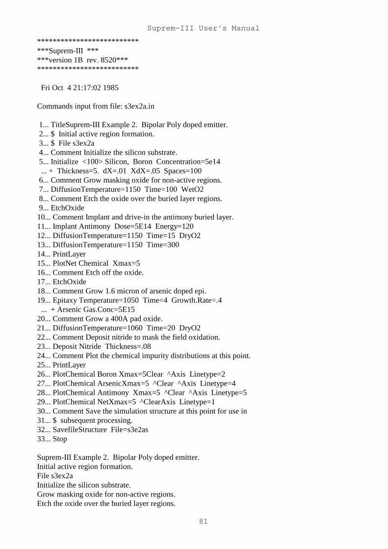
Suprem-III User's Manual
81
*****************************Suprem-III ******version 1B rev. 8520*****************************
Fri Oct 4 21:17:02 1985
Commands input from file: s3ex2a.in
1... TitleSuprem-III Example 2. Bipolar Poly doped emitter. 2... $ Initial active region formation. 3... $ File s3ex2a 4... Comment Initialize the silicon substrate. 5... Initialize <100> Silicon, Boron Concentration=5e14 ... + Thickness=5. dX=.01 XdX=.05 Spaces=100 6... Comment Grow masking oxide for non-active regions. 7... DiffusionTemperature=1150 Time=100 WetO2 8... Comment Etch the oxide over the buried layer regions. 9... EtchOxide10... Comment Implant and drive-in the antimony buried layer.11... Implant Antimony Dose=5E14 Energy=12012... DiffusionTemperature=1150 Time=15 DryO213... DiffusionTemperature=1150 Time=30014... PrintLayer15... PlotNet Chemical Xmax=516... Comment Etch off the oxide.17... EtchOxide18... Comment Grow 1.6 micron of arsenic doped epi.19... Epitaxy Temperature=1050 Time=4 Growth.Rate=.4 ... + Arsenic Gas.Conc=5E1520... Comment Grow a 400A pad oxide.21... DiffusionTemperature=1060 Time=20 DryO222... Comment Deposit nitride to mask the field oxidation.23... Deposit Nitride Thickness=.0824... Comment Plot the chemical impurity distributions at this point.25... PrintLayer26... PlotChemical Boron Xmax=5Clear ^Axis Linetype=227... PlotChemical ArsenicXmax=5 ^Clear ^Axis Linetype=428... PlotChemical Antimony Xmax=5 ^Clear ^Axis Linetype=529... PlotChemical NetXmax=5 ^ClearAxis Linetype=130... Comment Save the simulation structure at this point for use in31... $ subsequent processing.32... SavefileStructure File=s3e2as33... Stop
Suprem-III Example 2. Bipolar Poly doped emitter.Initial active region formation.File s3ex2aInitialize the silicon substrate.Grow masking oxide for non-active regions.Etch the oxide over the buried layer regions.

Suprem-III User's Manual
82
Implant and drive-in the antimony buried layer.
layer material type thickness dx dxmin top bottom orientationno. (microns) (microns) node node or grain size2 OXIDE 0.0692 0.0100 0.0010 422 4241 SILICON 4.5442 0.0100 0.0010 425 500 <100>
Integrated Dopantlayer Net Totalno. active chemical active chemical2 0.e+00 9.4142e+11 0.e+00 9.4788e+111 4.8900e+14 4.8900e+14 4.8942e+14 4.8942e+14
sum 4.8900e+14 4.8994e+14 4.8942e+14 4.9037e+14
Integrated Dopantlayer BORON ANTIMONYno. active chemical active chemical2 0.e+00 3.2324e+09 0.e+00 9.4465e+111 2.1123e+11 2.1123e+11 4.8921e+14 4.8921e+14
sum 2.1123e+11 2.1446e+11 4.8921e+14 4.9015e+14
Junction Depths and Integrated DopantConcentrations for Each Diffused Region
layer region type junction depth net totalno. no. (microns) active Qd chemical Qd2 1 n 0. 0.e+00 9.4788e+111 2 n 0. 4.8909e+14 4.8931e+141 1 p 2.4666 9.6637e+10 1.0719e+11
Etch off the oxide.Grow 1.6 micron of arsenic doped epi.Grow a 400A pad oxide.Deposit nitride to mask the field oxidation.Plot the chemical impurity distributions at this point.
layer Materialtype
thickness dx dxmin top bottom orientation
no. (microns) (microns) node node or grain size3 NITRIDE 0.0800 0.0100 0.0010 291 2992 OXIDE 0.0408 0.0100 0.0010 300 3021 SILICON 6.1263 0.0100 0.0010 303 500 <100>
Integrated Dopantlayer Net Totalno. active chemical active chemical3 0.e+00 0.e+00 0.e+00 0.e+002 0.e+00 1.6043e+09 0.e+00 1.6043e+091 4.8681e+14 4.8681e+14 4.8724e+14 4.8724e+14
sum 4.8681e+14 4.8682e+14 4.8724e+14 4.8724e+14
Integrated Dopant
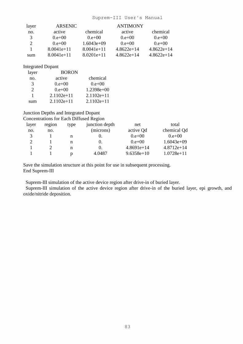
Suprem-III User's Manual
83
layer ARSENIC ANTIMONYno. active chemical active chemical3 0.e+00 0.e+00 0.e+00 0.e+002 0.e+00 1.6043e+09 0.e+00 0.e+001 8.0041e+11 8.0041e+11 4.8622e+14 4.8622e+14
sum 8.0041e+11 8.0201e+11 4.8622e+14 4.8622e+14
Integrated Dopantlayer BORONno. active chemical3 0.e+00 0.e+002 0.e+00 1.2398e+001 2.1102e+11 2.1102e+11
sum 2.1102e+11 2.1102e+11
Junction Depths and Integrated DopantConcentrations for Each Diffused Region
layer region type junction depth net totalno. no. (microns) active Qd chemical Qd3 1 n 0. 0.e+00 0.e+002 1 n 0. 0.e+00 1.6043e+091 2 n 0. 4.8691e+14 4.8712e+141 1 p 4.0487 9.6358e+10 1.0728e+11
Save the simulation structure at this point for use in subsequent processing.End Suprem-III
Suprem-III simulation of the active device region after drive-in of buried layer. Suprem-III simulation of the active device region after drive-in of the buried layer, epi growth, andoxide/nitride deposition.
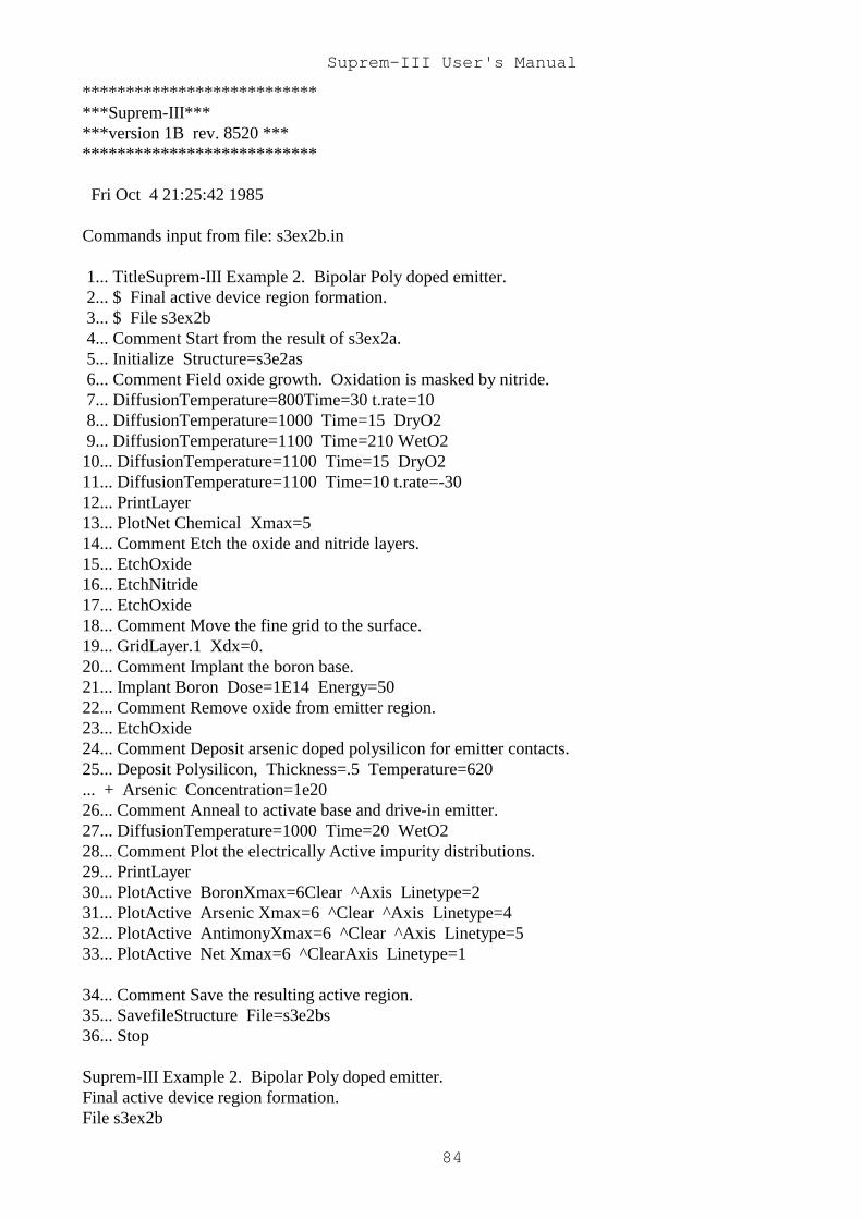
Suprem-III User's Manual
84
******************************Suprem-III******version 1B rev. 8520 ******************************
Fri Oct 4 21:25:42 1985
Commands input from file: s3ex2b.in
1... TitleSuprem-III Example 2. Bipolar Poly doped emitter. 2... $ Final active device region formation. 3... $ File s3ex2b 4... Comment Start from the result of s3ex2a. 5... Initialize Structure=s3e2as 6... Comment Field oxide growth. Oxidation is masked by nitride. 7... DiffusionTemperature=800Time=30 t.rate=10 8... DiffusionTemperature=1000 Time=15 DryO2 9... DiffusionTemperature=1100 Time=210 WetO210... DiffusionTemperature=1100 Time=15 DryO211... DiffusionTemperature=1100 Time=10 t.rate=-3012... PrintLayer13... PlotNet Chemical Xmax=514... Comment Etch the oxide and nitride layers.15... EtchOxide16... EtchNitride17... EtchOxide18... Comment Move the fine grid to the surface.19... GridLayer.1 Xdx=0.20... Comment Implant the boron base.21... Implant Boron Dose=1E14 Energy=5022... Comment Remove oxide from emitter region.23... EtchOxide24... Comment Deposit arsenic doped polysilicon for emitter contacts.25... Deposit Polysilicon, Thickness=.5 Temperature=620... + Arsenic Concentration=1e2026... Comment Anneal to activate base and drive-in emitter.27... DiffusionTemperature=1000 Time=20 WetO228... Comment Plot the electrically Active impurity distributions.29... PrintLayer30... PlotActive BoronXmax=6Clear ^Axis Linetype=231... PlotActive Arsenic Xmax=6 ^Clear ^Axis Linetype=432... PlotActive AntimonyXmax=6 ^Clear ^Axis Linetype=533... PlotActive Net Xmax=6 ^ClearAxis Linetype=1
34... Comment Save the resulting active region.35... SavefileStructure File=s3e2bs36... Stop
Suprem-III Example 2. Bipolar Poly doped emitter.Final active device region formation.File s3ex2b
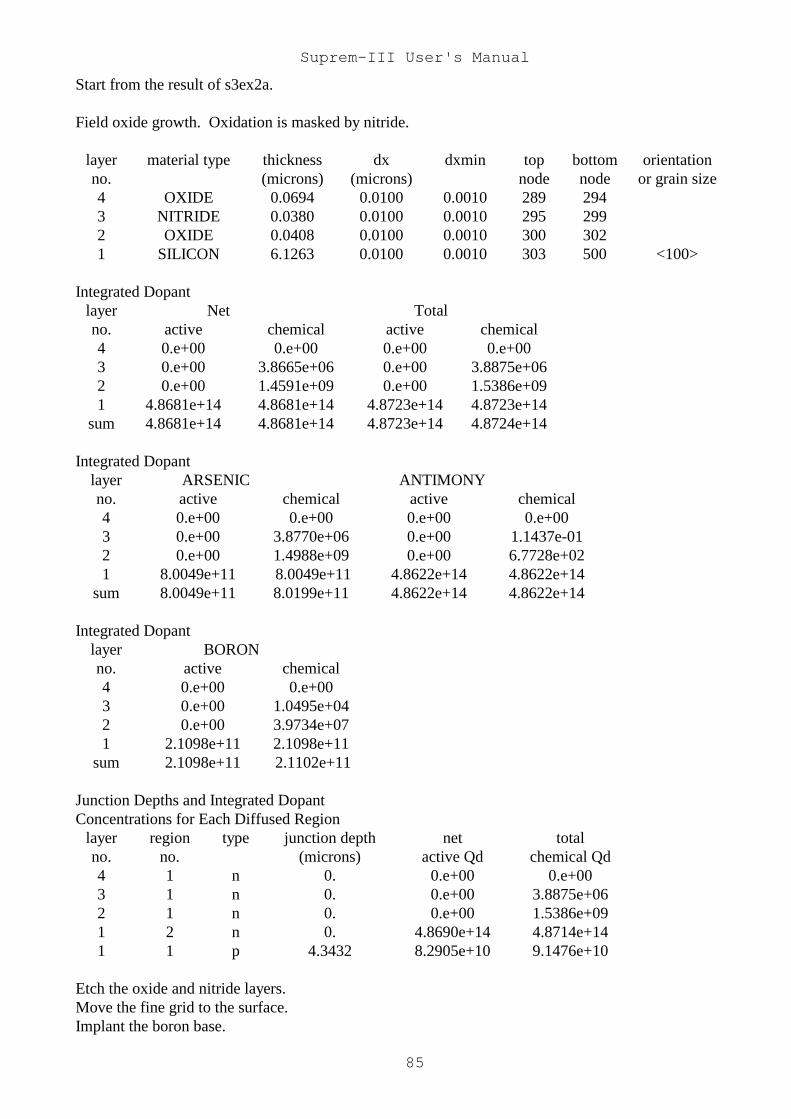
Suprem-III User's Manual
85
Start from the result of s3ex2a.
Field oxide growth. Oxidation is masked by nitride.
layer material type thickness dx dxmin top bottom orientationno. (microns) (microns) node node or grain size4 OXIDE 0.0694 0.0100 0.0010 289 2943 NITRIDE 0.0380 0.0100 0.0010 295 2992 OXIDE 0.0408 0.0100 0.0010 300 3021 SILICON 6.1263 0.0100 0.0010 303 500 <100>
Integrated Dopantlayer Net Totalno. active chemical active chemical4 0.e+00 0.e+00 0.e+00 0.e+003 0.e+00 3.8665e+06 0.e+00 3.8875e+062 0.e+00 1.4591e+09 0.e+00 1.5386e+091 4.8681e+14 4.8681e+14 4.8723e+14 4.8723e+14
sum 4.8681e+14 4.8681e+14 4.8723e+14 4.8724e+14
Integrated Dopantlayer ARSENIC ANTIMONYno. active chemical active chemical4 0.e+00 0.e+00 0.e+00 0.e+003 0.e+00 3.8770e+06 0.e+00 1.1437e-012 0.e+00 1.4988e+09 0.e+00 6.7728e+021 8.0049e+11 8.0049e+11 4.8622e+14 4.8622e+14
sum 8.0049e+11 8.0199e+11 4.8622e+14 4.8622e+14
Integrated Dopantlayer BORONno. active chemical4 0.e+00 0.e+003 0.e+00 1.0495e+042 0.e+00 3.9734e+071 2.1098e+11 2.1098e+11
sum 2.1098e+11 2.1102e+11
Junction Depths and Integrated DopantConcentrations for Each Diffused Region
layer region type junction depth net totalno. no. (microns) active Qd chemical Qd4 1 n 0. 0.e+00 0.e+003 1 n 0. 0.e+00 3.8875e+062 1 n 0. 0.e+00 1.5386e+091 2 n 0. 4.8690e+14 4.8714e+141 1 p 4.3432 8.2905e+10 9.1476e+10
Etch the oxide and nitride layers.Move the fine grid to the surface.Implant the boron base.
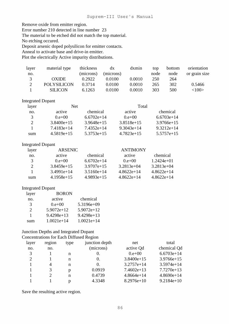
Suprem-III User's Manual
86
Remove oxide from emitter region.Error number 210 detected in line number 23The material to be etched did not match the top material.No etching occured.Deposit arsenic doped polysilicon for emitter contacts.Anneal to activate base and drive-in emitter.Plot the electrically Active impurity distributions.
layer material type thickness dx dxmin top bottom orientationno. (microns) (microns) node node or grain size3 OXIDE 0.2922 0.0100 0.0010 250 2642 POLYSILICON 0.3714 0.0100 0.0010 265 302 0.54661 SILICON 6.1263 0.0100 0.0010 303 500 <100>
Integrated Dopantlayer Net Totalno. active chemical active chemical3 0.e+00 6.6702e+14 0.e+00 6.6703e+142 3.8400e+15 3.9648e+15 3.8518e+15 3.9766e+151 7.4183e+14 7.4352e+14 9.3043e+14 9.3212e+14
sum 4.5819e+15 5.3753e+15 4.7823e+15 5.5757e+15
Integrated Dopantlayer ARSENIC ANTIMONYno. active chemical active chemical3 0.e+00 6.6702e+14 0.e+00 1.2424e+012 3.8459e+15 3.9707e+15 3.2813e+04 3.2813e+041 3.4991e+14 3.5160e+14 4.8622e+14 4.8622e+14
sum 4.1958e+15 4.9893e+15 4.8622e+14 4.8622e+14
Integrated Dopantlayer BORONno. active chemical3 0.e+00 5.3196e+092 5.9072e+12 5.9072e+121 9.4298e+13 9.4298e+13
sum 1.0021e+14 1.0021e+14
Junction Depths and Integrated DopantConcentrations for Each Diffused Region
layer region type junction depth net totalno. no. (microns) active Qd chemical Qd3 1 n 0. 0.e+00 6.6703e+142 1 n 0. 3.8400e+15 3.9766e+151 4 n 0. 3.2757e+14 3.5974e+141 3 p 0.0919 7.4602e+13 7.7270e+131 2 n 0.4739 4.8664e+14 4.8690e+141 1 p 4.3348 8.2976e+10 9.2184e+10
Save the resulting active region.
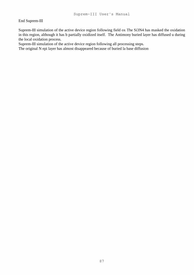
Suprem-III User's Manual
87
End Suprem-III
Suprem-III simulation of the active device region following field ox The Si3N4 has masked the oxidationin this region, although it has b partially oxidized itself. The Antimony buried layer has diffused u duringthe local oxidation process.Suprem-III simulation of the active device region following all processing steps.The original N epi layer has almost disappeared because of buried la base diffusion
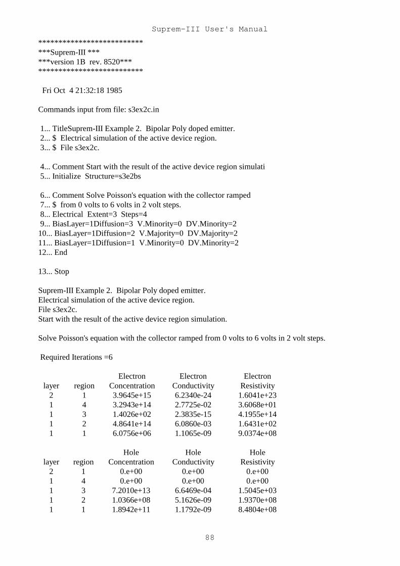
Suprem-III User's Manual
88
*****************************Suprem-III ******version 1B rev. 8520*****************************
Fri Oct 4 21:32:18 1985
Commands input from file: s3ex2c.in
1... TitleSuprem-III Example 2. Bipolar Poly doped emitter. 2... $ Electrical simulation of the active device region. 3... $ File s3ex2c.
4... Comment Start with the result of the active device region simulati 5... Initialize Structure=s3e2bs
6... Comment Solve Poisson's equation with the collector ramped 7... $ from 0 volts to 6 volts in 2 volt steps. 8... Electrical Extent=3 Steps=4 9... BiasLayer=1Diffusion=3 V.Minority=0 DV.Minority=210... BiasLayer=1Diffusion=2 V.Majority=0 DV.Majority=211... BiasLayer=1Diffusion=1 V.Minority=0 DV.Minority=212... End
13... Stop
Suprem-III Example 2. Bipolar Poly doped emitter.Electrical simulation of the active device region.File s3ex2c.Start with the result of the active device region simulation.
Solve Poisson's equation with the collector ramped from 0 volts to 6 volts in 2 volt steps.
Required Iterations =6
Electron Electron Electronlayer region Concentration Conductivity Resistivity
2 1 3.9645e+15 6.2340e-24 1.6041e+231 4 3.2943e+14 2.7725e-02 3.6068e+011 3 1.4026e+02 2.3835e-15 4.1955e+141 2 4.8641e+14 6.0860e-03 1.6431e+021 1 6.0756e+06 1.1065e-09 9.0374e+08
Hole Hole Holelayer region Concentration Conductivity Resistivity
2 1 0.e+00 0.e+00 0.e+001 4 0.e+00 0.e+00 0.e+001 3 7.2010e+13 6.6469e-04 1.5045e+031 2 1.0366e+08 5.1626e-09 1.9370e+081 1 1.8942e+11 1.1792e-09 8.4804e+08
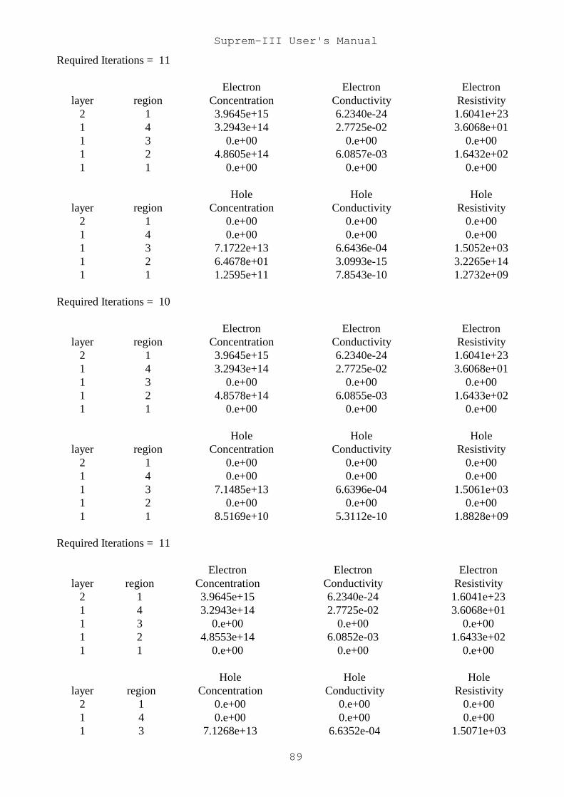
Suprem-III User's Manual
89
Required Iterations = 11
Electron Electron Electronlayer region Concentration Conductivity Resistivity
2 1 3.9645e+15 6.2340e-24 1.6041e+231 4 3.2943e+14 2.7725e-02 3.6068e+011 3 0.e+00 0.e+00 0.e+001 2 4.8605e+14 6.0857e-03 1.6432e+021 1 0.e+00 0.e+00 0.e+00
Hole Hole Holelayer region Concentration Conductivity Resistivity
2 1 0.e+00 0.e+00 0.e+001 4 0.e+00 0.e+00 0.e+001 3 7.1722e+13 6.6436e-04 1.5052e+031 2 6.4678e+01 3.0993e-15 3.2265e+141 1 1.2595e+11 7.8543e-10 1.2732e+09
Required Iterations = 10
Electron Electron Electronlayer region Concentration Conductivity Resistivity
2 1 3.9645e+15 6.2340e-24 1.6041e+231 4 3.2943e+14 2.7725e-02 3.6068e+011 3 0.e+00 0.e+00 0.e+001 2 4.8578e+14 6.0855e-03 1.6433e+021 1 0.e+00 0.e+00 0.e+00
Hole Hole Holelayer region Concentration Conductivity Resistivity
2 1 0.e+00 0.e+00 0.e+001 4 0.e+00 0.e+00 0.e+001 3 7.1485e+13 6.6396e-04 1.5061e+031 2 0.e+00 0.e+00 0.e+001 1 8.5169e+10 5.3112e-10 1.8828e+09
Required Iterations = 11
Electron Electron Electronlayer region Concentration Conductivity Resistivity
2 1 3.9645e+15 6.2340e-24 1.6041e+231 4 3.2943e+14 2.7725e-02 3.6068e+011 3 0.e+00 0.e+00 0.e+001 2 4.8553e+14 6.0852e-03 1.6433e+021 1 0.e+00 0.e+00 0.e+00
Hole Hole Holelayer region Concentration Conductivity Resistivity
2 1 0.e+00 0.e+00 0.e+001 4 0.e+00 0.e+00 0.e+001 3 7.1268e+13 6.6352e-04 1.5071e+03

Suprem-III User's Manual
90
1 2 0.e+00 0.e+00 0.e+001 1 5.2488e+10 3.2732e-10 3.0551e+09
End Suprem-III
Plot of base region sheet resistance vs. collector base voltage base upon a Suprem-III Poisson solutionthrough the active device region.
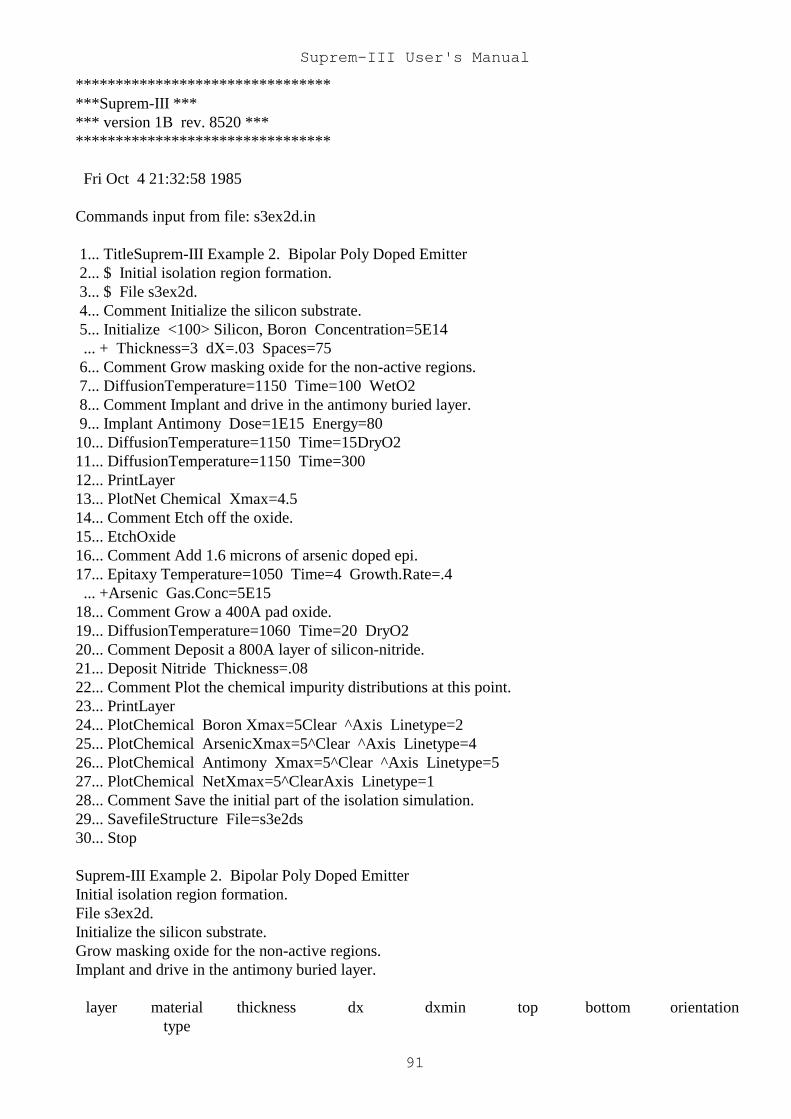
Suprem-III User's Manual
91
***********************************Suprem-III ****** version 1B rev. 8520 ***********************************
Fri Oct 4 21:32:58 1985
Commands input from file: s3ex2d.in
1... TitleSuprem-III Example 2. Bipolar Poly Doped Emitter 2... $ Initial isolation region formation. 3... $ File s3ex2d. 4... Comment Initialize the silicon substrate. 5... Initialize <100> Silicon, Boron Concentration=5E14 ... + Thickness=3 dX=.03 Spaces=75 6... Comment Grow masking oxide for the non-active regions. 7... DiffusionTemperature=1150 Time=100 WetO2 8... Comment Implant and drive in the antimony buried layer. 9... Implant Antimony Dose=1E15 Energy=8010... DiffusionTemperature=1150 Time=15DryO211... DiffusionTemperature=1150 Time=30012... PrintLayer13... PlotNet Chemical Xmax=4.514... Comment Etch off the oxide.15... EtchOxide16... Comment Add 1.6 microns of arsenic doped epi.17... Epitaxy Temperature=1050 Time=4 Growth.Rate=.4 ... +Arsenic Gas.Conc=5E1518... Comment Grow a 400A pad oxide.19... DiffusionTemperature=1060 Time=20 DryO220... Comment Deposit a 800A layer of silicon-nitride.21... Deposit Nitride Thickness=.0822... Comment Plot the chemical impurity distributions at this point.23... PrintLayer24... PlotChemical Boron Xmax=5Clear ^Axis Linetype=225... PlotChemical ArsenicXmax=5^Clear ^Axis Linetype=426... PlotChemical Antimony Xmax=5^Clear ^Axis Linetype=527... PlotChemical NetXmax=5^ClearAxis Linetype=128... Comment Save the initial part of the isolation simulation.29... SavefileStructure File=s3e2ds30... Stop
Suprem-III Example 2. Bipolar Poly Doped EmitterInitial isolation region formation.File s3ex2d.Initialize the silicon substrate.Grow masking oxide for the non-active regions.Implant and drive in the antimony buried layer.
layer materialtype
thickness dx dxmin top bottom orientation
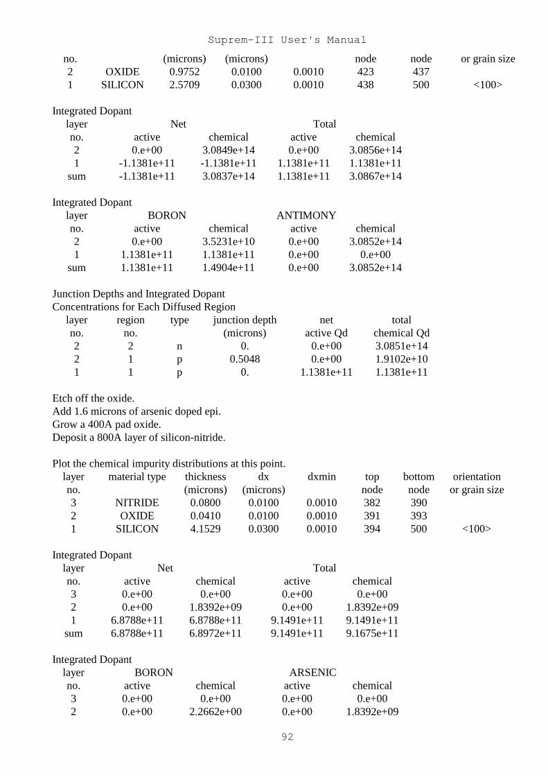
Suprem-III User's Manual
92
no. (microns) (microns) node node or grain size2 OXIDE 0.9752 0.0100 0.0010 423 4371 SILICON 2.5709 0.0300 0.0010 438 500 <100>
Integrated Dopantlayer Net Totalno. active chemical active chemical2 0.e+00 3.0849e+14 0.e+00 3.0856e+141 -1.1381e+11 -1.1381e+11 1.1381e+11 1.1381e+11
sum -1.1381e+11 3.0837e+14 1.1381e+11 3.0867e+14
Integrated Dopantlayer BORON ANTIMONYno. active chemical active chemical2 0.e+00 3.5231e+10 0.e+00 3.0852e+141 1.1381e+11 1.1381e+11 0.e+00 0.e+00
sum 1.1381e+11 1.4904e+11 0.e+00 3.0852e+14
Junction Depths and Integrated DopantConcentrations for Each Diffused Region
layer region type junction depth net totalno. no. (microns) active Qd chemical Qd2 2 n 0. 0.e+00 3.0851e+142 1 p 0.5048 0.e+00 1.9102e+101 1 p 0. 1.1381e+11 1.1381e+11
Etch off the oxide.Add 1.6 microns of arsenic doped epi.Grow a 400A pad oxide.Deposit a 800A layer of silicon-nitride.
Plot the chemical impurity distributions at this point.layer material type thickness dx dxmin top bottom orientationno. (microns) (microns) node node or grain size3 NITRIDE 0.0800 0.0100 0.0010 382 3902 OXIDE 0.0410 0.0100 0.0010 391 3931 SILICON 4.1529 0.0300 0.0010 394 500 <100>
Integrated Dopantlayer Net Totalno. active chemical active chemical3 0.e+00 0.e+00 0.e+00 0.e+002 0.e+00 1.8392e+09 0.e+00 1.8392e+091 6.8788e+11 6.8788e+11 9.1491e+11 9.1491e+11
sum 6.8788e+11 6.8972e+11 9.1491e+11 9.1675e+11
Integrated Dopantlayer BORON ARSENICno. active chemical active chemical3 0.e+00 0.e+00 0.e+00 0.e+002 0.e+00 2.2662e+00 0.e+00 1.8392e+09
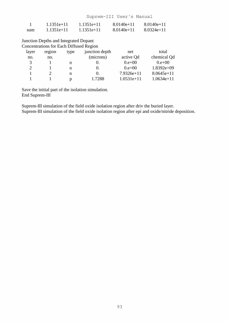
Suprem-III User's Manual
93
1 1.1351e+11 1.1351e+11 8.0140e+11 8.0140e+11sum 1.1351e+11 1.1351e+11 8.0140e+11 8.0324e+11
Junction Depths and Integrated DopantConcentrations for Each Diffused Region
layer region type junction depth net totalno. no. (microns) active Qd chemical Qd3 1 n 0. 0.e+00 0.e+002 1 n 0. 0.e+00 1.8392e+091 2 n 0. 7.9326e+11 8.0645e+111 1 p 1.7288 1.0531e+11 1.0634e+11
Save the initial part of the isolation simulation.End Suprem-III
Suprem-III simulation of the field oxide isolation region after driv the buried layer.Suprem-III simulation of the field oxide isolation region after epi and oxide/nitride deposition.
Suprem-III User's Manual
94
************************* ***** Suprem-III ******version 1B rev. 8520******************************
Fri Oct 4 21:35:35 1985
Commands input from file: s3ex2e.in
1... TitleSuprem-III Example 2. Bipolar Poly doped emitter. 2... $ Final isolation region formation. 3... $ File s3ex2e. 4... Comment Start with the result of S3EX2D. 5... Initialize Structure=s3e2ds Thickness=6 6... Comment Etch the nitride and oxide layers. 7... EtchNitride 8... EtchOxide 9... Comment Etch half the silicon epi layer.10... EtchSilicon Amount=.811... Comment Implant boron in the field region.12... Implant Boron Dose=2E13 Energy=10013... Comment Grow the field oxide.14... DiffusionTemperature=800Time=30 T.Rate=1015... DiffusionTemperature=1100 Time=15DryO216... DiffusionTemperature=1100 Time=210 WetO217... DiffusionTemperature=1100 Time=15DryO218... DiffusionTemperature=1100 Time=10 T.Rate=-3019... PrintLayer20... Comment Implant the boron base.21... Implant Boron Dose=1E14 Energy=8022... Comment Deposit arsenic doped polysilicon for the emitter contact.23... Deposit Polysilicon, Thickness=.5 Temperature=620. ...+ Arsenic Concentration=1E2024... Comment Remove the polysilicon.25... EtchPolysilicon26... Comment Anneal to activate base and emitter regions.27... DiffusionTemperature=1000 Time=20 WetO228... Comment Plot the electrically active impurity distributions.29... PrintLayer30... PlotActive BoronXmax=5Clear ^Axis Linetype=231... PlotActive Arsenic Xmax=5^Clear ^Axis Linetype=432... PlotActive AntimonyXmax=5^Clear ^Axis Linetype=533... PlotActive Net Xmax=5^ClearAxis Linetype=134... Comment Save the final isolation region simulation.35... SavefileStructure File=s3e2es36... Stop
Suprem-III Example 2. Bipolar Poly doped emitter.Final isolation region formation.File s3ex2e.Start with the result of S3EX2D.
Suprem-III User's Manual
95
Etch the nitride and oxide layers.Etch half the silicon epi layer.Implant boron in the field region.Grow the field oxide.
layer material type thickness dx dxmin top bottom orientationno. (microns) (microns) node node or grain size2 OXIDE 1.2357 0.0100 0.0010 412 4271 SILICON 4.6563 0.0300 0.0010 428 500 <100>
Integrated Dopantlayer Net Totalno. active chemical active chemical2 0.e+00 -1.3771e+13 0.e+00 1.4035e+131 -4.9493e+12 -4.9493e+12 5.4422e+12 5.4422e+12
sum -4.9493e+12 -1.8720e+13 5.4422e+12 1.9478e+13
Integrated Dopantlayer BORON ARSENICno. active chemical active chemical2 0.e+00 1.3903e+13 0.e+00 1.3241e+111 5.1957e+12 5.1957e+12 2.4646e+11 2.4646e+11
sum 5.1957e+12 1.9099e+13 2.4646e+11 3.7886e+11
Junction Depths and Integrated DopantConcentrations for Each Diffused Region
layer region type junction depth net totalno. no. (microns) active Qd chemical Qd2 1 p 0. 0.e+00 1.4035e+131 2 n 0. 1.5444e+10 5.6460e+101 1 p 0.0452 4.9231e+12 5.3460e+12
Implant the boron base.Deposit arsenic doped polysilicon for the emitter contact.Remove the polysilicon.Anneal to activate base and emitter regions.Plot the electrically active impurity distributions.Layer material type thickness dx dxmin top bottom orientation
no. (microns) (microns) node node or grain size2 OXIDE 1.2689 0.0100 0.0010 412 4271 SILICON 4.6417 0.0300 0.0010 428 500 <100>
Integrated Dopantlayer Net Totalno. active chemical active chemical2 0.e+00 -1.1433e+14 0.e+00 1.1460e+141 -4.8363e+12 -4.8363e+12 5.3259e+12 5.3259e+12
sum -4.8363e+12 -1.1917e+14 5.3259e+12 1.1993e+14Integrated Dopant
layer BORON ARSENICno. active chemical active chemical2 0.e+00 1.1447e+14 0.e+00 1.3411e+111 5.0811e+12 5.0811e+12 2.4476e+11 2.4476e+11
Suprem-III User's Manual
96
sum 5.0811e+12 1.1955e+14 2.4476e+11 3.7886e+11Junction Depths and Integrated DopantConcentrations for Each Diffused Region
layer region type junction depth net totalno. no. (microns) active Qd chemical Qd2 1 p 0. 0.e+00 1.1460e+141 1 p 0. 4.8363e+12 5.3259e+12
Save the final isolation region simulation.End Suprem-III
Suprem-III simulation through the field oxide isolation region after processing steps. Isolation has beenachieved since the substrate i p type, although barely. The base implant is also seen in the field
XLVII. Suggestions and Bug Reports
In any program of the size of Suprem-III there is bound to be at least one bug (Do I hear somelaughter?). And even if everything works as claimed, there will always be room for improvement. Therefore, I am listing both an electronic and U.S. mail address for such things as bug reports, suggestions,complaints, and compliments (if any).
Please send as much detail as possible about the problem and especially indicate which version ofthe program you are using and what system you are working on.
Electronic MailU.S Mail
sup3bugs@SU-FujiSuprem-III c/o Stephen E. Hansen Applied Electronics Labs Stanford University Stanford, California 94305
If you can manage it I really prefer electronic mail as it makes response easier. In either case theresponse time will depend on a number of factors, primarily the severity of the problem.
Your feedback is critical and appreciated!
Thanks,
Stephen E. Hansen