
Supplementary Materials for...Fig. S1. Schematic of the device and the processing temperatures of...
14
www.sciencemag.org/cgi/content/full/science.aao5561/DC1 Supplementary Materials for A generic interface to reduce the efficiency-stability-cost gap of perovskite solar cells Yi Hou,* Xiaoyan Du, Simon Scheiner, David P. McMeekin, Zhiping Wang, Ning Li, Manuela S. Killian, Haiwei Chen, Moses Richter, Ievgen Levchuk, Nadine Schrenker, Erdmann Spiecker, Tobias Stubhan, Norman A. Luechinger, Andreas Hirsch, Patrik Schmuki, Hans-Peter Steinrück, Rainer H. Fink, Marcus Halik, Henry J. Snaith, Christoph J. Brabec* *Corresponding author. Email: [email protected] (Y.H.); [email protected] (C.J.B) Published 9 November 2017 on Science First Release DOI: 10.1126/science.aao5561 This PDF file includes: Materials and Methods Figs. S1 to S13 Tables S1 to S4
Transcript of Supplementary Materials for...Fig. S1. Schematic of the device and the processing temperatures of...
www.sciencemag.org/cgi/content/full/science.aao5561/DC1
Supplementary Materials for
A generic interface to reduce the efficiency-stability-cost gap of
perovskite solar cells
Yi Hou,* Xiaoyan Du, Simon Scheiner, David P. McMeekin, Zhiping Wang, Ning Li,
Manuela S. Killian, Haiwei Chen, Moses Richter, Ievgen Levchuk, Nadine Schrenker,
Erdmann Spiecker, Tobias Stubhan, Norman A. Luechinger, Andreas Hirsch, Patrik
Schmuki, Hans-Peter Steinrück, Rainer H. Fink, Marcus Halik, Henry J. Snaith,
Christoph J. Brabec*
*Corresponding author. Email: [email protected] (Y.H.); [email protected] (C.J.B)
Published 9 November 2017 on Science First Release
DOI: 10.1126/science.aao5561
This PDF file includes:
Materials and Methods
Figs. S1 to S13
Tables S1 to S4
Materials and Methods
Materials and Preparation
Unless stated otherwise, all materials were purchased from Sigma Aldrich or Merck and used as
received. MAI, FAI, PbBr2, and PbI2, was purchased from Lumtec and Dyesol. To form a 1.4 M
MAPbI3 precursor solution, PbI2 and MAI were mixed with a mole ratio of 1:1 in a mixture of
DMF and DMSO (4:1 v/v). A 1.4 M FA0.83MA0.17Pb1.1Br0.50I2.80 precursor solution was similarly
prepared using a mixture of DMF and DMSO (4:1 v/v). The dry WOx and Ta-WOx nano powders
were prepared via flame spray synthesis using a precursor solution of tungsten and tantalum salts
in organic solvents. The precursor then was fed to a spray nozzle, dispersed by oxygen and ignited
by a premixed methane-oxygen flame. The off-gas was filtered through a steel mesh filter (20
micron mesh size) by a vacuum pump. The WOx and Ta-WOx nano powder obtained was collected
from the filter mesh. A stable suspension was prepared by dispersing the nano powder in ethanol
or isopropanol respectively using an undisclosed dispersant (proprietary information of Avantama
Ltd.). The P3HT, PTB7, pDPP5T-2, PffBT4T-2OD, PDBT-T1 and PDCBT were dissolved in
chlorobenzene or chloroform at concentrations of 5 mg/mL, and followed by stirring on a 60 °C
hot plate for 2 hours.
Solar cell fabrication
First, the patterned ITO substrates were ultrasonically cleaned using acetone and isopropanol for
10 minutes each. On each cleaned ITO substrate, a dense and smooth layer of C60-SAM was
deposited by dipping the ITO substrate into the C60-SAM solution for 24 hours. The SnOx layer
was prepared by spinning SnCl4.5H2O precursor in IPA (17.5mg/mL) at 3000 r.p.m. for 30s and
annealed the film at 140 °C for 45 min. 10 mg/mL PCBM solution in CB was deposited on to the
SnOx at a speed of 4000 r.p.m for 20 s. The as-prepared perovskite precursor solution was filtered
using a 0.45 µm PTFE syringe filter and coated onto substrates at a speed of 4000 r.p.m for 20 s.
The substrate (around 2.5 cm×2.5 cm) was quenched by CB solvent and annealed on a hot plate at
100 ◦C for 10 min in N2. The prepared polymer HTMs were spin-coated at 1000 r.p.m for 35 s.
Subsequently, Ta-WOx and WOx were coated onto polymer HTMs at a speed of 2000 r.p.m for 30
s. Finally, a 100-nm-thick Au counter electrode was deposited onto a hole-transporting layer
through a shadow mask by thermal evaporation.
Device characterizations
j-V characteristics of all the devices were measured using a source measurement unit from BoTest.
Illumination was provided by a Newport Sol1A solar simulator with AM 1.5G spectrum and light
intensity of 100 mWcm-2, which was determined by a calibrated crystalline Si-cell. During device
characterization, a shadow mask with an opening of 10 mm2 was used. For stability test, the
illumination was provided by a white LED (XLamp CXA2011 1300K CCT) and its intensity was
adjusted in a way that the generated photocurrent matched the one under a solar simulator. The
moisture and O2 concentrations were kept below 0.5 p.p.m. for the ageing experiments in N2
atmosphere at room temperature.
Material characterization
External quantum efficiency (EQE) spectra were recorded using an Enli Technology (Taiwan)
EQE measurement system (QE-R), and the light intensity at each wavelength was calibrated using
a standard single-crystal Si photovoltaic cell.
X-ray photoelectron spectroscopy (XPS) measurements were conducted in an ultrahigh vacuum
(UHV) chamber with a base pressure below 5×10⁻¹⁰ mbar using a Scienta ESCA 200 spectrometer
with a monochromatic Al Kα X-ray source (1486.6 eV) and a hemispherical electron energy
analyzer.
Ultraviolet photoelectron spectroscopy (UPS) measurements were performed in the same chamber
with a He I UV source, applying a – 5.00 V bias to the sample. The work function is calculated as
the energetic difference between the Fermi level and the vacuum level, as defined by the
secondary-electron edge. The ionization energy is estimated as the onset of the density of states at
the top of the valence band. Reported results were repeated on at least three spots per sample.
Scanning electron microscopy (SEM): A FEI Helios Nanolab 660 was used to acquire scanning
electron microscopy (SEM) images and to prepare FIB cross-sections. The final polishing with the
ion beam was performed at 30 kV and 80 pA. The SEM micrographs of the cross-sections as well
as the plan view samples were recorded at an acceleration voltage of 2 kV with a current of 100
pA.
X-ray powder diffraction (XRD): X-ray diffraction analysis was performed by classical ex situ
Bragg – Brentano geometry using a Panalytical X'pert powder diffractometer with filtered Cu-Kα
radiation and an X'Celerator solid-state stripe detector.
Time-of-flight secondary ion mass spectrometry (ToF-SIMS) was performed on a ToF-SIMS 5
spectrometer (ION-TOF; Munster, Germany) using 25 keV Bi+ bunched down to <0.8 ns. The
primary ion dose density for spectra acquisition was 5 × 10¹¹ ions cm-2 with an area of 100 µm ×
100 µm using negative polarity. Spectra were normalized to their total intensity and calibrated on
C−, O−, C2−, C2H
−, and C3−. Depth profiles were carried out with a crater size of 250 µm × 250 µm
and a measured spot of 50 µm × 50 µm in the center of crater. The sputter beam used was Cs 500
eV and the measurement beam was Bi+ using negative polarity. The interlaced mode was used
with 5s of sputtering and 1s flooding with low energy electrons for charge neutralization. Reported
results were repeated on at least three spots per sample.
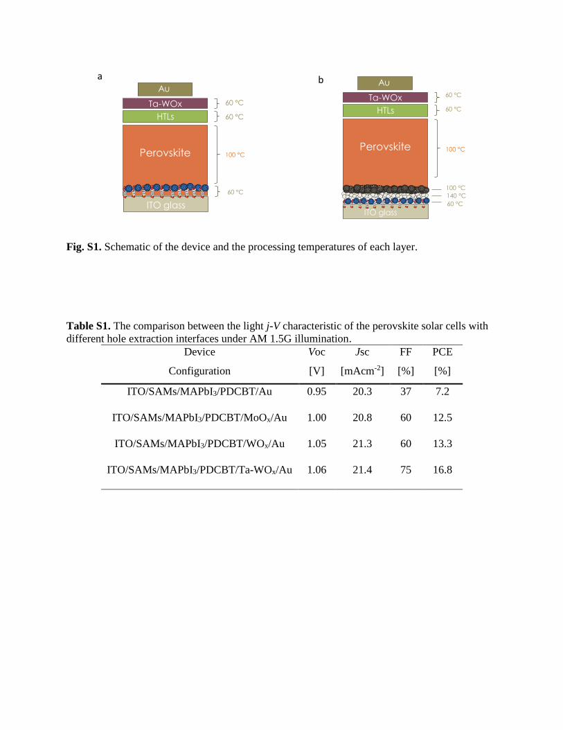
Fig. S1. Schematic of the device and the processing temperatures of each layer.
Table S1. The comparison between the light j-V characteristic of the perovskite solar cells with
different hole extraction interfaces under AM 1.5G illumination.
Device
Configuration
Voc
[V]
Jsc
[mAcm-2]
FF
[%]
PCE
[%]
ITO/SAMs/MAPbI3/PDCBT/Au 0.95 20.3 37 7.2
ITO/SAMs/MAPbI3/PDCBT/MoOx/Au 1.00 20.8 60 12.5
ITO/SAMs/MAPbI3/PDCBT/WOx/Au 1.05 21.3 60 13.3
ITO/SAMs/MAPbI3/PDCBT/Ta-WOx/Au 1.06 21.4 75 16.8
ITO glass
Perovskite
HTLs
Au
Ta-WOx
60 °C
100 °C
60 °C
60 °C
Perovskite
HTLs
Au
Ta-WOx
100 °C
100 °C
60 °C
60 °C
ITO glass
140 °C
60 °C
a b
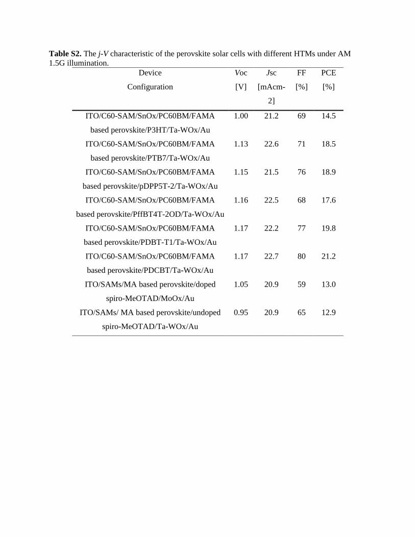
Table S2. The j-V characteristic of the perovskite solar cells with different HTMs under AM
1.5G illumination.
Device
Configuration
Voc
[V]
Jsc
[mAcm-
2]
FF
[%]
PCE
[%]
ITO/C60-SAM/SnOx/PC60BM/FAMA
based perovskite/P3HT/Ta-WOx/Au
1.00 21.2 69 14.5
ITO/C60-SAM/SnOx/PC60BM/FAMA
based perovskite/PTB7/Ta-WOx/Au
1.13 22.6 71 18.5
ITO/C60-SAM/SnOx/PC60BM/FAMA
based perovskite/pDPP5T-2/Ta-WOx/Au
1.15 21.5 76 18.9
ITO/C60-SAM/SnOx/PC60BM/FAMA
based perovskite/PffBT4T-2OD/Ta-WOx/Au
1.16 22.5 68 17.6
ITO/C60-SAM/SnOx/PC60BM/FAMA
based perovskite/PDBT-T1/Ta-WOx/Au
1.17 22.2 77 19.8
ITO/C60-SAM/SnOx/PC60BM/FAMA
based perovskite/PDCBT/Ta-WOx/Au
1.17 22.7 80 21.2
ITO/SAMs/MA based perovskite/doped
spiro-MeOTAD/MoOx/Au
1.05 20.9 59 13.0
ITO/SAMs/ MA based perovskite/undoped
spiro-MeOTAD/Ta-WOx/Au
0.95 20.9 65 12.9
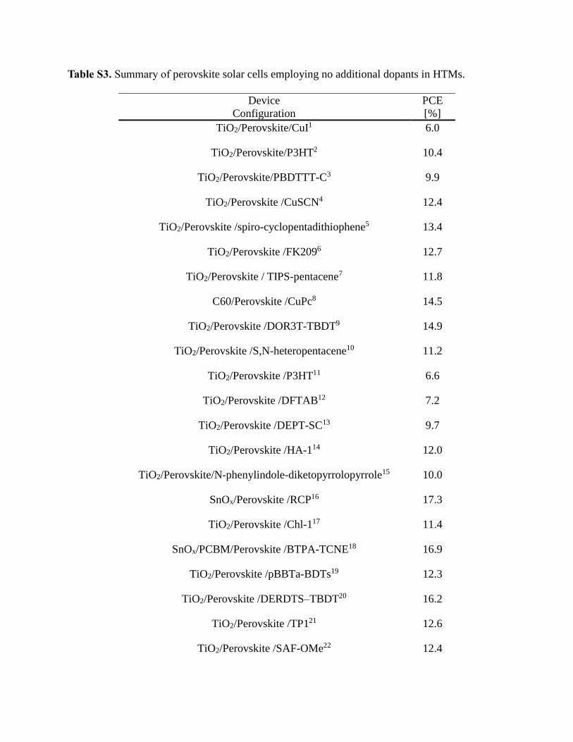
Table S3. Summary of perovskite solar cells employing no additional dopants in HTMs.
Device
Configuration
PCE
[%]
TiO2/Perovskite/CuI1 6.0
TiO2/Perovskite/P3HT2 10.4
TiO2/Perovskite/PBDTTT-C3 9.9
TiO2/Perovskite /CuSCN4 12.4
TiO2/Perovskite /spiro-cyclopentadithiophene5 13.4
TiO2/Perovskite /FK2096 12.7
TiO2/Perovskite / TIPS-pentacene7 11.8
C60/Perovskite /CuPc8 14.5
TiO2/Perovskite /DOR3T-TBDT9 14.9
TiO2/Perovskite /S,N-heteropentacene10 11.2
TiO2/Perovskite /P3HT11 6.6
TiO2/Perovskite /DFTAB12 7.2
TiO2/Perovskite /DEPT-SC13 9.7
TiO2/Perovskite /HA-114 12.0
TiO2/Perovskite/N-phenylindole-diketopyrrolopyrrole15 10.0
SnOx/Perovskite /RCP16 17.3
TiO2/Perovskite /Chl-117 11.4
SnOx/PCBM/Perovskite /BTPA-TCNE18 16.9
TiO2/Perovskite /pBBTa-BDTs19 12.3
TiO2/Perovskite /DERDTS–TBDT20 16.2
TiO2/Perovskite /TP121 12.6
TiO2/Perovskite /SAF-OMe22 12.4
TiO2/Perovskite /TPE-4DPA23 9.1
TiO2/Perovskite /HTM Z3424 16.1
TiO2/Perovskite /Z101125 16.3
TiO2/Perovskite /ST126 15.4
TiO2/Perovskite /DPP27 10.8
TiO2/Perovskite/KR32128 19.0
Trux-OMeTAD/Perovskite/PCBM/ZnO29 18.6
PTAA/Perovskite/PS/C60/BCP30 20.4
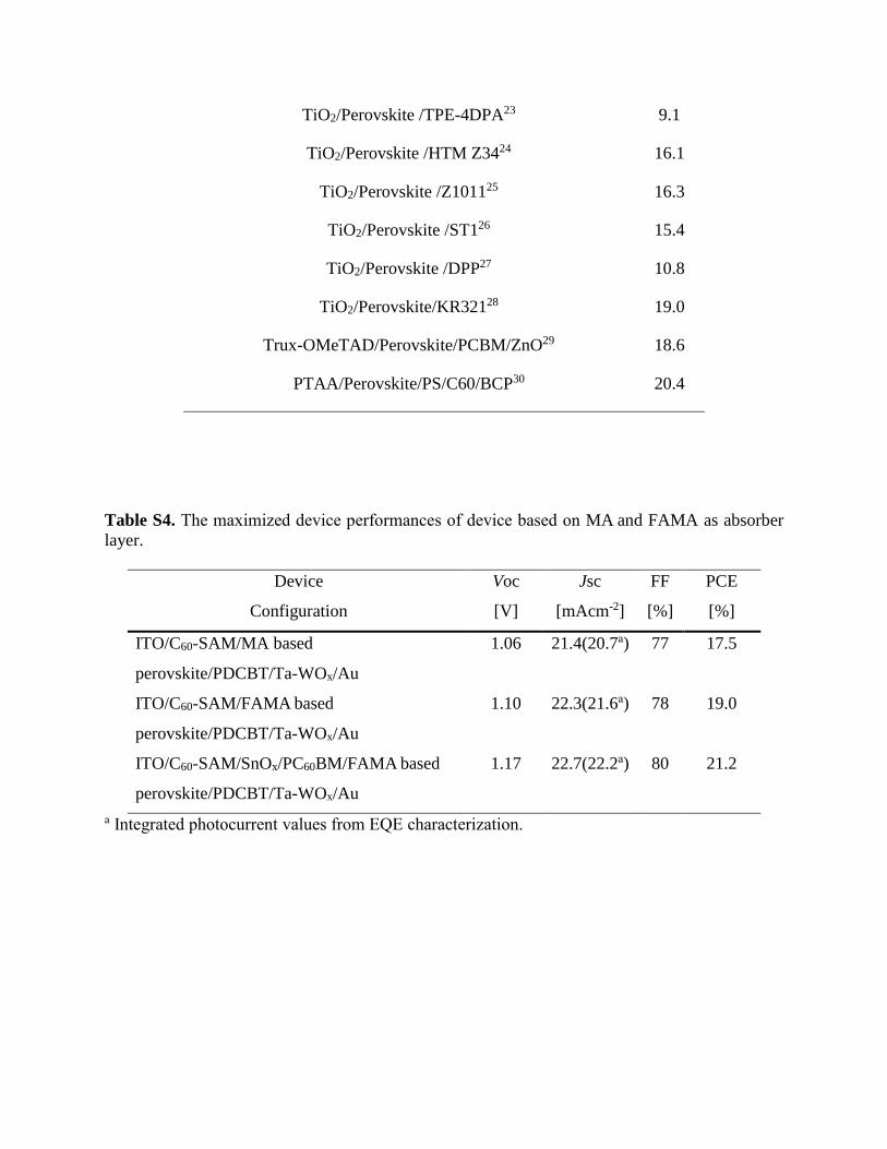
Table S4. The maximized device performances of device based on MA and FAMA as absorber
layer.
Device
Configuration
Voc
[V]
Jsc
[mAcm-2]
FF
[%]
PCE
[%]
ITO/C60-SAM/MA based
perovskite/PDCBT/Ta-WOx/Au
1.06 21.4(20.7a) 77 17.5
ITO/C60-SAM/FAMA based
perovskite/PDCBT/Ta-WOx/Au
ITO/C60-SAM/SnOx/PC60BM/FAMA based
perovskite/PDCBT/Ta-WOx/Au
1.10
1.17
22.3(21.6a)
22.7(22.2a)
78
80
19.0
21.2
a Integrated photocurrent values from EQE characterization.

Fig. S2. UV-vis absorption spectra of glass/WOx and glass/Ta-WOx, and the corresponding real
pictures of these two inks.
Fig. S3. XPS spectra of WOx and Ta-WOx.
400 600 800 1000 1200 14000.0
0.1
0.2
WOx
Ta-WOx
Wavelength (nm)
Ab
so
rba
nce
Ta-WOx WOx
32 31 30 29 28 27 26 25
Ta(V) 4f7/2
Inte
nsity (
a.u
.)
Binding Energy (eV)
WOx
Ta-WOx
Ta(V) 4f5/2
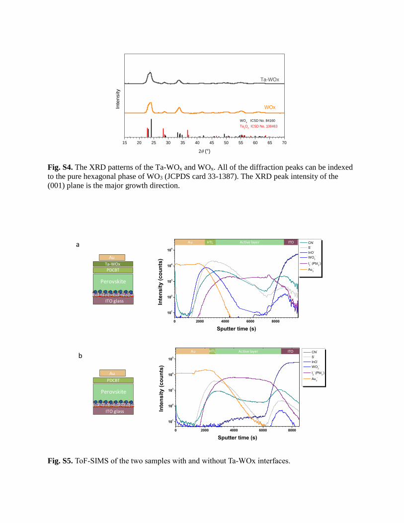
Fig. S4. The XRD patterns of the Ta-WOx and WOx. All of the diffraction peaks can be indexed
to the pure hexagonal phase of WO3 (JCPDS card 33-1387). The XRD peak intensity of the
(001) plane is the major growth direction.
Fig. S5. ToF-SIMS of the two samples with and without Ta-WOx interfaces.
ITO glass
Perovskite
PDCBT
Au
Ta-WOx
0 2000 4000 6000 8000
101
102
103
104
105
CN-
S-
InO-
WO3
-
I2
- (PbI
3
-)
Au3
-
Inte
nsit
y (
co
un
ts)
Sputter time (s)
Au Active layer ITO
0 2000 4000 6000 8000
101
102
103
104
105
CN-
S-
InO-
WO3
-
I2
- (PbI
3
-)
Au3
-
Inte
nsit
y (
co
un
ts)
Sputter time (s)
HTL
Au Active layer ITOHTLa
b
ITO glass
Perovskite
PDCBT
Au
15 20 25 30 35 40 45 50 55 60 65 70
(001)
24.0
WO3 ICSD No. 84160
Ta2O
5 ICSD No. 108463
In
ten
sity
2 (°)
23.8
(001)
WOx
Ta-WOx
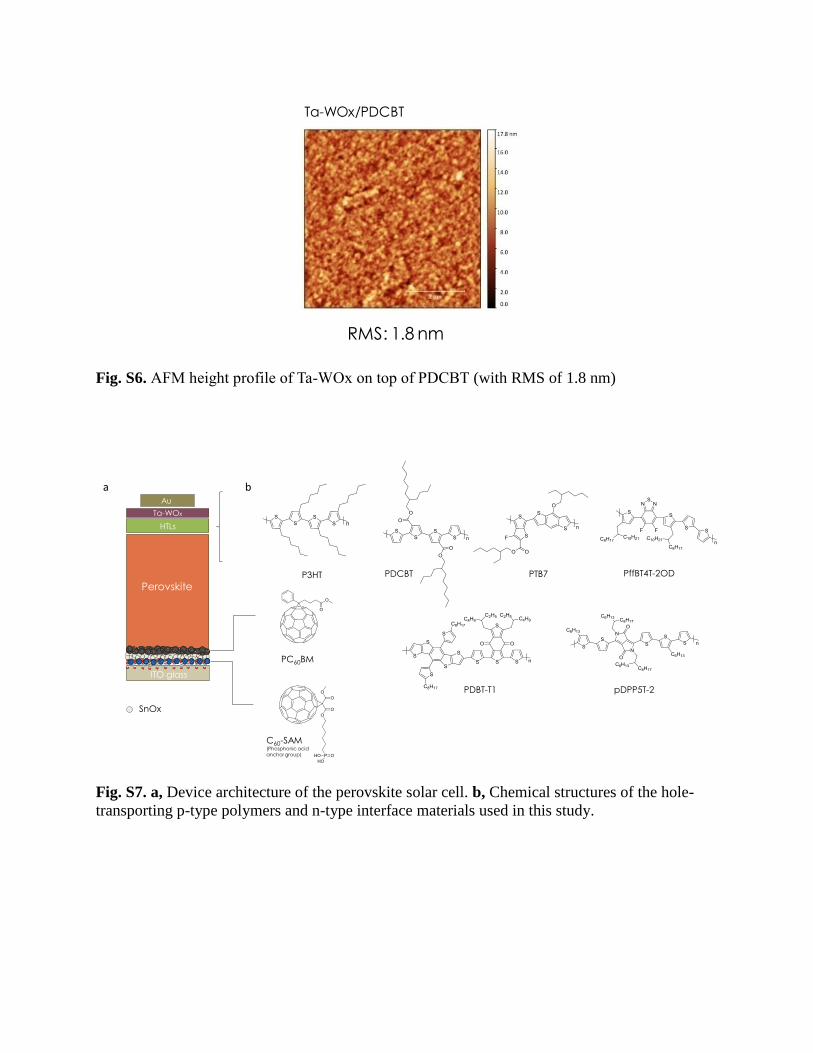
Fig. S6. AFM height profile of Ta-WOx on top of PDCBT (with RMS of 1.8 nm)
Fig. S7. a, Device architecture of the perovskite solar cell. b, Chemical structures of the hole-
transporting p-type polymers and n-type interface materials used in this study.
RMS: 1.8 nm
Ta-WOx/PDCBT
ITO glass
Perovskite
HTLs
Au
Ta-WOx
PDCBTP3HT
pDPP5T-2
C60-SAM(Phosphonic acid anchor group)
SnOx
PTB7
PC60BM
PffBT4T-2OD
PDBT-T1
a b
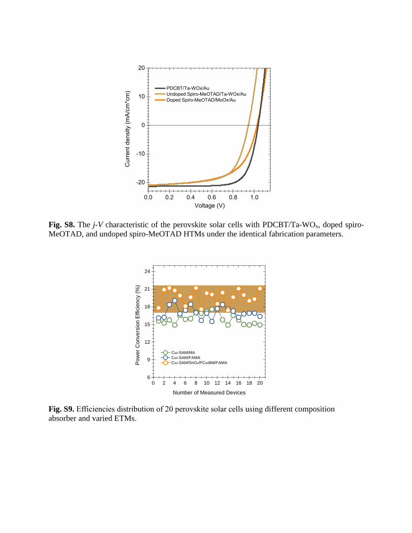
Fig. S8. The j-V characteristic of the perovskite solar cells with PDCBT/Ta-WOx, doped spiro-
MeOTAD, and undoped spiro-MeOTAD HTMs under the identical fabrication parameters.
0 2 4 6 8 10 12 14 16 18 206
9
12
15
18
21
24
C60-SAM/MA
C60-SAM/FAMA
C60-SAM/SnOx/PC60BM/FAMA
Po
we
r C
on
ve
rsio
n E
ffic
ien
cy (
%)
Number of Measured Devices
Fig. S9. Efficiencies distribution of 20 perovskite solar cells using different composition
absorber and varied ETMs.
0.0 0.2 0.4 0.6 0.8 1.0
-20
-10
0
10
20
PDCBT/Ta-WOx/Au
Undoped Spiro-MeOTAD/Ta-WOx/Au
Doped Spiro-MeOTAD/MoOx/Au
Voltage (V)
Cu
rre
nt d
en
sity (
mA
/cm
*cm
)

400 500 600 700 800 900 1000 1100
MA
FAMA
Wavelength (nm)
Norm
aliz
ed
abso
rbance
Fig. S10. UV-vis absorption spectra of FAMA and MA based perovskite, respectively.
400 500 600 700 8000
20
40
60
80
100
Inte
gra
ted
Cu
rre
nt
(mA
/cm
2)
Wavelength (nm)
Exte
rna
l Q
ua
ntu
m E
ffic
ien
cy (
%)
0
5
10
15
20
25
30
MA
FAMA
Fig. S11. EQE and integrated current spectrum of the devices with FAMA and MA based
perovskite as absorber layer.
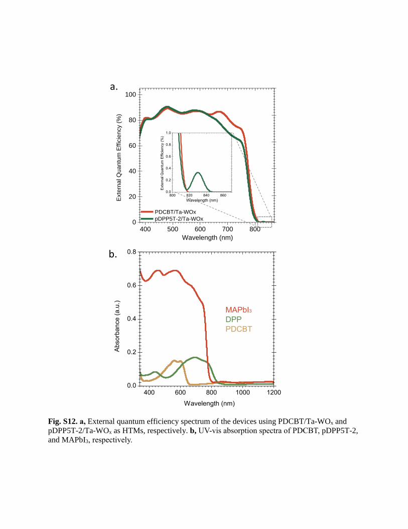
Fig. S12. a, External quantum efficiency spectrum of the devices using PDCBT/Ta-WOx and
pDPP5T-2/Ta-WOx as HTMs, respectively. b, UV-vis absorption spectra of PDCBT, pDPP5T-2,
and MAPbI3, respectively.
400 600 800 1000 12000.0
0.2
0.4
0.6
0.8
Wavelength (nm)
Absorb
ance (
a.u
.)
MAPbI3
DPP
PDCBT
400 500 600 700 8000
20
40
60
80
100
PDCBT/Ta-WOx
pDPP5T-2/Ta-WOx
Wavelength (nm)
Exte
rna
l Q
ua
ntu
m E
ffic
ien
cy (
%)
800 820 840 8600.0
0.2
0.4
0.6
0.8
1.0
Wavelength (nm)
Exte
rnal Q
uantu
m E
ffic
iency (
%)
a.
b.
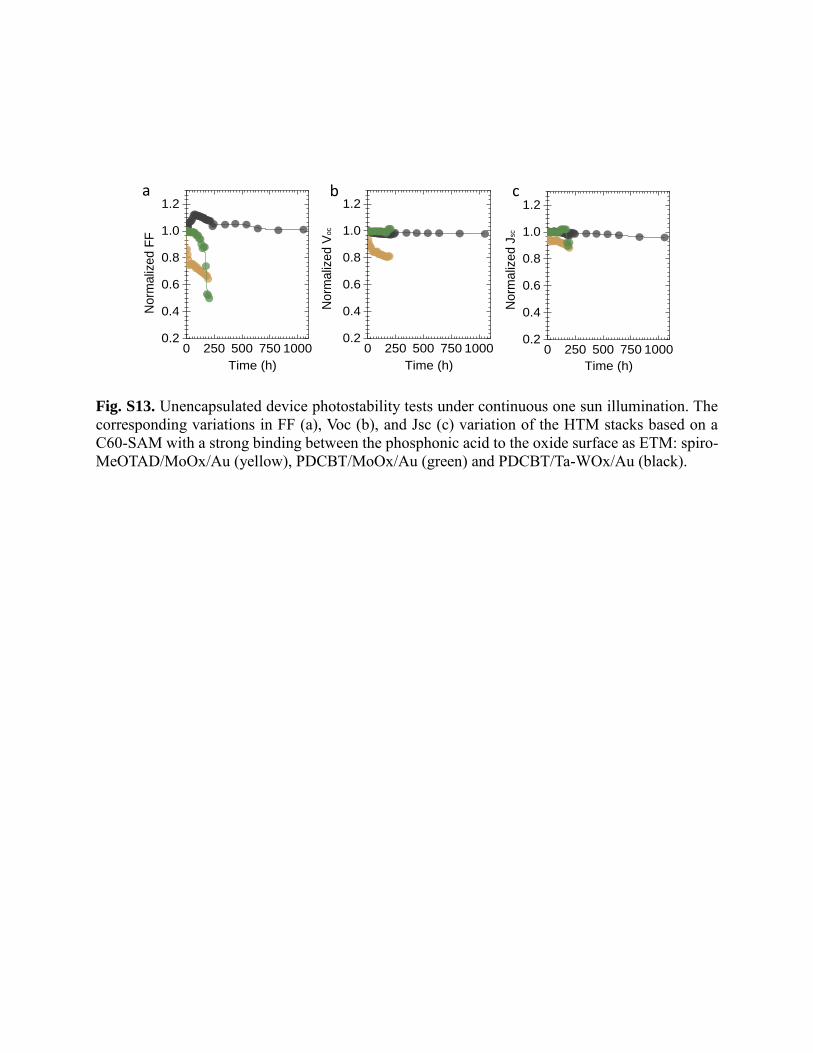
Fig. S13. Unencapsulated device photostability tests under continuous one sun illumination. The
corresponding variations in FF (a), Voc (b), and Jsc (c) variation of the HTM stacks based on a
C60-SAM with a strong binding between the phosphonic acid to the oxide surface as ETM: spiro-
MeOTAD/MoOx/Au (yellow), PDCBT/MoOx/Au (green) and PDCBT/Ta-WOx/Au (black).
0 250 500 750 10000.2
0.4
0.6
0.8
1.0
1.2
No
rmaliz
ed F
F
Time (h)
0 250 500 750 10000.2
0.4
0.6
0.8
1.0
1.2
No
rmaliz
ed V
oc
Time (h)
0 250 500 750 10000.2
0.4
0.6
0.8
1.0
1.2
No
rma
lize
d J
sc
Time (h)
cba