SUPPLEMENTARY INFORMATION - media.nature.com · 3 . I. Preparation and characterization of graphene...
25
Switching terahertz waves with gate-controlled active graphene metamaterials Seung Hoon Lee, Muhan Choi, Teun-Teun Kim, Seungwoo Lee, Ming Liu, Xiaobo Yin, Hong Kyw Choi, Seung S. Lee, Choon-Gi Choi, Sung-Yool Choi, Xiang Zhang & Bumki Min I. Preparation and characterization of graphene A. CVD growth of SLG and MLG and their transfer method B. Characterization of CVD-grown graphene II. Transparent EOT gate electrode A. Design of EOT electrode B. Polarization dependency III. Study on MLG metamaterials A. Amplitude and phase modulation IV. Study on SLG metamaterials A. Simulation method B. Modulation speed C. Mitigation of large voltage requirement D. Humidity effect on memory performance E. Reproducibility SUPPLEMENTARY INFORMATION DOI: 10.1038/NMAT3433 NATURE MATERIALS | www.nature.com/naturematerials 1 © 2012 Macmillan Publishers Limited. All rights reserved.
Transcript of SUPPLEMENTARY INFORMATION - media.nature.com · 3 . I. Preparation and characterization of graphene...
1
Switching terahertz waves with gate-controlled active graphene metamaterials
Seung Hoon Lee, Muhan Choi, Teun-Teun Kim, Seungwoo Lee, Ming Liu, Xiaobo Yin,
Hong Kyw Choi, Seung S. Lee, Choon-Gi Choi, Sung-Yool Choi, Xiang Zhang & Bumki
Min
I. Preparation and characterization of graphene A. CVD growth of SLG and MLG and their transfer method B. Characterization of CVD-grown graphene
II. Transparent EOT gate electrode A. Design of EOT electrode B. Polarization dependency
III. Study on MLG metamaterials A. Amplitude and phase modulation
IV. Study on SLG metamaterials A. Simulation method B. Modulation speed C. Mitigation of large voltage requirement D. Humidity effect on memory performance E. Reproducibility
SUPPLEMENTARY INFORMATIONDOI: 10.1038/NMAT3433
NATURE MATERIALS | www.nature.com/naturematerials 1
© 2012 Macmillan Publishers Limited. All rights reserved.

2
Figure S1 | Schematics of the gate-controlled active graphene metamaterials and their optical images a, Schematic view on fabrication of the active graphene metamaterial (PI: polyimide, td: total device thickness). b, Optical micrographs of the fabricated hexagonal meta-atoms c, Asymmetric double split ring (aDSR) meta-atoms.
2 NATURE MATERIALS | www.nature.com/naturematerials
SUPPLEMENTARY INFORMATION DOI: 10.1038/NMAT3433
© 2012 Macmillan Publishers Limited. All rights reserved.

3
I. Preparation and characterization of graphene
A. CVD growth of SLG and MLG and their transfer method
For the fabrication of samples, we used commercially available single-layer graphene
(SLG) from GRAPHENE SQUARE Inc., and multilayer graphene (MLG) grown by in-
house thermal chemical vapour deposition (CVD). For MLG growth, 300-nm-thick
nickel was deposited as a catalyst layer on a SiO2/Si substrate by an electron-beam
evaporator. Prepared Ni/SiO2/Si substrate was loaded in a quartz tube furnace, then
heated up to 1,000 °C under vacuum condition (30 mTorr) with a constant H2 flow (10
sccm). MLG was grown by flowing gas mixtures (CH4:H2 / 30:10 sccm) for 3 min and
MLG on the substrate was dismounted from the furnace and cooled down to room
temperature (25 °C) at a cooling rate of 5 °C/min under Ar gas flow of 1,000 sccm.
In order to transfer the CVD-grown SLG and MLG to a polyimide substrate, a
polydimethylsiloxane (PDMS) film was used to minimize undesired cracks and solvent-
induced effects. The thermally grown SLG (MLG) on the Cu foil (Ni/SiO2/Si substrate)
was peeled off from the substrate after 8-hour etching in a 0.1 mol% ammonium
persulfate (3-hour etching in a 12.5 mol% iron chloride) solution. After a two-step
rinsing process with DI water, the graphene layer was successfully transferred and
conformally attached to the prepared polyimide layer, on which the meta-atoms were
patterned.
B. Characterization of CVD-grown graphene
Confirmation of Single-Layer Graphene Raman spectroscopy was used with a 532
nm excitation laser for the characterization of graphene layers. The SLG, grown in the
same batch for samples used in the main manuscript, was transferred onto a 300-nm-thick
SiO2 substrate. The representative features of the SLG can be summarized as follows [1];
(1) The 2D-peak over G-peak intensity ratio (I2D/IG) is generally in the range between 2
and 4, (2) The full width at half maximum (FWHM) of 2D-peak is about ~30 cm-1. As
NATURE MATERIALS | www.nature.com/naturematerials 3
SUPPLEMENTARY INFORMATIONDOI: 10.1038/NMAT3433
© 2012 Macmillan Publishers Limited. All rights reserved.

4
shown in Fig. S2a, the location and FWHM of 2D peak of CVD-grown is 2,686 cm-1 and
30 cm-1, respectively. To further investigate the graphene’s quality, we have also
conducted Raman spectroscopic mapping of I2D/IG for CVD-grown graphene over an
arbitrarily chosen area of 20 × 20 μm2, and the data are presented in Fig. S2c. For
comparison, the mapping of I2D/IG is also added for a mechanically exfoliated graphene
in Figs. S2b and d.
Figure S2 | Comparison between CVD-grown graphene and mechanically exfoliated graphene a, Raman intensity plot of CVD-grown graphene shows that 2D peak is located at 2,686 cm-1 with the FWHM of about 30 cm-1. b, Raman intensity plot for mechanically exfoliated graphene, c, Mapping of Raman intensity ratio of G-peak to 2D-peak (I2D/IG) for arbitrarily chosen area of 20 × 20 μm2 of CVD-grown graphene and d, mechanically exfoliated graphene on a 300-nm-thick SiO2 substrate.
4 NATURE MATERIALS | www.nature.com/naturematerials
SUPPLEMENTARY INFORMATION DOI: 10.1038/NMAT3433
© 2012 Macmillan Publishers Limited. All rights reserved.

5
Amount of Doping In the main manuscript, we have estimated the doping level
(carrier density as a function of gate voltage) of the graphene integrated into the device in
Fig. 2f. It is generally known that during the synthesis and additional fabrication
processes CVD-grown graphene is in a p-doped state. For our graphene in the device, the
hole density under the condition at Vg = 0 V was estimated to be ~2.99 × 1012 cm-2 from
the gate capacitance in the electron charge (α = 8.54 × 109 cm-2V-1) and the measured
charge neutral gate voltage VCNP. Therefore, we have concluded that the corresponding
Fermi level of graphene inside the device was about -203 meV at Vg = 0 V.
For direct estimation of the amount of doping in CVD-grown graphene on a SiO2
substrate, we conducted further measurements using Raman spectroscopy as with the
work by Basko et al [2]. In their method, the doping level can be estimated non-
destructively by the ratio of the integrated area under 2D to that of G-peak (denoted as
A2D/AG) in the Raman spectra. Figures S3a and b show the measured spectrally-
integrated area ratio of 2D-peak to G-peak (A2D/AG) of the CVD-grown graphene on a
SiO2 substrate with the value of mechanically exfoliated graphene. The value of A2D/AG
for CVD-grown graphene is measured at about 2.8 while the value (A2D/AG) for
exfoliated graphene is slightly above 5. From the A2D/AG versus doping level plot from
the reference [2], we could estimate the doping level of the CVD-grown as -250 meV,
while that of mechanically exfoliated graphene as -100 meV. The doping level of CVD-
grown graphene on the SiO2 substrate (EF = -250 meV) is estimated to be slightly higher
than that of the graphene imbedded in the polyimide-based metamaterial (EF = -203
meV). This difference can be attributed to the following factors; (1) device (graphene)
variation as can be seen in the reference [2], (2) dependence on the substrate (i.e., SiO2
versus polyimide), (3) single-side versus double-side coverage of dielectric materials, and
(4) different method of graphene preparation.
We have also estimated the doping level using the other method established by Das et al.
[3]. The method is based on the measurement of the ratio of 2D- to G-peak intensity
(I2D/IG). In our graphene metamaterial, the doping level was comparable with the value
in the reference.
NATURE MATERIALS | www.nature.com/naturematerials 5
SUPPLEMENTARY INFORMATIONDOI: 10.1038/NMAT3433
© 2012 Macmillan Publishers Limited. All rights reserved.

6
Figure S3 | Raman mapping images Area ratio A2D/AG of a, CVD-grown graphene and b, mechanically exfoliated graphene as a reference sample. Intensity ratio ID/IG for c, the CVD-grown and d, exfoliated graphene.
Amount of Defects The D-peak is a crucial measure for the quantitative estimation of
the amount of defects, because the breathing modes of hexagonal carbon ring,
represented by D-peak, cannot be excited without defects. The relation between the
amount of defect and the intensity ratio of D-peak to G-peak (denoted as ID/IG) was
thoroughly discussed in the reference [4]. In Figs. S3c and d, the ID/IG mapping data for
the arbitrarily chosen area of 20 × 20 μm2 of CVD-grown graphene (mechanically
exfoliated graphene) shows that the average values of ID/IG is given by 0.287 (0.0441).
From that result, we have estimated the distance between point-like defects in graphene
of LD = 19.0 ~ 25.3 nm (48.6 ~ 64.6 nm) and the defect density of nD = 4.96 ~ 8.77 × 10¹⁰
cm-2 (0.76 ~ 1.35 × 1010 cm-2), respectively. Since ID/IG value corresponds to two
different defect densities, it is therefore necessary to use additional information such as
6 NATURE MATERIALS | www.nature.com/naturematerials
SUPPLEMENTARY INFORMATION DOI: 10.1038/NMAT3433
© 2012 Macmillan Publishers Limited. All rights reserved.

7
the FWHM of G-peak. The FWHM of G peak in our CVD-grown graphene (single layer
part) has a value < 15 cm-1, which allow the distance LD to be determined unambiguously
[4]. To conclude, from the evaluation of the intensity ratio of D- to G-peak, our CVD-
grown graphene turns out to be more defective and its defect density (single layer part) is
at least 6.5 times larger than that of the reference sample (exfoliated graphene).
Multilayer graphene Raman spectroscopy of MLG shows that the number of layer
varies spatially and is estimated to be approximately 1 to 10, as confirmed by
transmission electron micrographs (TEM) as shown in Fig. S4. A cross-sectional TEM
image of the fabricated MLG metamaterial shows that there are several discontinuities
with defects sites, such as gaps and wrinkles, which can be attributed to the one of the
dominant causes of electrically controlled photonic memory effects.
NATURE MATERIALS | www.nature.com/naturematerials 7
SUPPLEMENTARY INFORMATIONDOI: 10.1038/NMAT3433
© 2012 Macmillan Publishers Limited. All rights reserved.

8
Figure S4 | Characterization of MLG by Raman spectroscopy and transmission electron microscopy (TEM) a, OM image and b, Raman spectrum of MLG shows that the FWMH of 2D peak is larger than 45 cm-1. c, A cross-sectional TEM image of the MLG metamaterial. Between the polyimide layer and metallic meta-atoms, layered graphene is clearly identified. d, Average intensity profile across the graphene layer marked by red arrows.
8 NATURE MATERIALS | www.nature.com/naturematerials
SUPPLEMENTARY INFORMATION DOI: 10.1038/NMAT3433
© 2012 Macmillan Publishers Limited. All rights reserved.

9
II. Transparent EOT gate electrode
A. Design of EOT electrode
The gate electrode for the active graphene metamaterial was designed to apply a uniform
electric field in the graphene layer while maintaining a large transmission of terahertz
waves. In order to satisfy this requirement, an array of deep subwavelength-scale metallic
wires, referred to as an EOT electrode, was optimized. Figure S5a shows the schematics
(inset) of the EOT electrode dimension with numerically calculated transmission at
terahertz frequencies (0 – 2 THz). The EOT electrodes for the sample were fabricated
with the periodicity (a) of 6 μm and the gap width (a - wm) of 2 μm. Although the gap
width of the wire array is in the deep subwavelength-scale (~λ/150 at 1 THz), the
simulated transmission is found to be over 89% in the frequency band of interest. This
large transmission can be explained on the basis of well-known phenomena of
extraordinary optical transmission [5].
In addition, we have conducted finite element analysis using COMSOL Multiphysics and
calculated the gate-induced electric potential distribution inside the graphene
metamaterial. As illustrated by the flattened light blue area in the vicinity of graphene
(marked by the deep blue colour, Figs. S5b-d), the EOT gate electrode (even with low
width, 2 μm) can clearly induce a uniform static electric field in the vicinity of the
graphene layer.
NATURE MATERIALS | www.nature.com/naturematerials 9
SUPPLEMENTARY INFORMATIONDOI: 10.1038/NMAT3433
© 2012 Macmillan Publishers Limited. All rights reserved.

10
Figure S5 | EOT electrode design for the gate-controlled graphene metamaterials a, Schematic rendering of EOT electrodes along with simulated transmission spectra for metallic wire widths (wm) of 3, 4, and 5 m. b-d, Electric potential distribution in the periodic EOT electrode as function of wm when applying Vg = 100 V (periodicity a = 6 μm, device thickness t = 4 μm, and spacing s = 2 μm). Nearly uniform electric potential is distributed in the graphene layer which is conformally deposited onto the hexagonal meta-atoms.
10 NATURE MATERIALS | www.nature.com/naturematerials
SUPPLEMENTARY INFORMATION DOI: 10.1038/NMAT3433
© 2012 Macmillan Publishers Limited. All rights reserved.

11
B. Polarization dependency
Figure S6 | Polarization dependent transmission characteristics of the gate-controlled active SLG metamaterials The polarization dependency of graphene metamaterials is attributed to the polarization dependent transmission through the EOT electrode a, Schematic rendering of an active graphene metamaterial with only a EOT electrode. b-d, Polarization dependent transmission through the active graphene metamaterials as a function of gate voltage.
NATURE MATERIALS | www.nature.com/naturematerials 11
SUPPLEMENTARY INFORMATIONDOI: 10.1038/NMAT3433
© 2012 Macmillan Publishers Limited. All rights reserved.

12
III. Study on MLG metamaterials
A. Amplitude and phase modulation
Figure S7 | Amplitude and phase modulation of terahertz waves with the gate-controlled active MLG metamaterial a, Measured transmission spectra and their phase change as a function of ∆V (= VCNP - Vg) from 0 to 120 V. With increasing gate voltage, the resonant frequency was red-shifted and broadened by Joule losses in the graphene layer. Relative change in transmission (-∆T/TCNP) and phase change (∆ϕ) exceeded -138% and /3 radians at 120 V, respectively. b, For comparison, the simulated results of the active graphene metamaterials are plotted as a function of the Fermi level in a graphene layer (Here, we assumed the intraband scattering time of 25 fs and zero carrier density at conductivity minimum).
12 NATURE MATERIALS | www.nature.com/naturematerials
SUPPLEMENTARY INFORMATION DOI: 10.1038/NMAT3433
© 2012 Macmillan Publishers Limited. All rights reserved.

13
IV. Study on SLG metamaterials
A. Simulation method
For the modelling of gate-controlled active graphene metamaterials, we employed finite
element analysis provided by the commercially-available CST MICROWAVE STUDIO.
Frequency-dependent material parameters (complex permittivity) of gold at terahertz
frequencies were taken from the literature [6] and those of polyimide were taken from a
previously reported paper [7]. The complex dielectric constants of gold for the frequency
range of interest (0.1 ~ 2.5 THz) can be fitted by using the Drude model with a plasma
frequency of ωp = 1.37 × 10¹⁶ rad/s and collision frequency of γ = 4.07 × 10¹³ rad/s. For
the simulation of a unit cell, the periodic boundary condition is applied. After running
the finite element simulations with the appropriate boundary conditions, S-parameters
(transmission and reflection) were carefully extracted from the simulation results.
For graphene, Kubo formula was used to model the gate-variable complex optical
conductivity of graphene, σ(ω) = σintra(ω) + σinter(ω), where intraband transitions are the
dominant factors in the terahertz regime. The formulae for complex conductivity of
graphene are given as follows [8],
σ������ω� � � ���� � �� ���∆������������������ ���� � ��� � ���� � �����
∆ ,
σ������ω� � �����
������� � �� �� � ∆�
��� ���� � ��� � ��� � �����∆ .
Here, ��� � ��� is the Fermi distribution function with Fermi energy ��, � describes the
broadening of the interband transitions, � is the momentum relaxation time due to carrier
intraband scattering, and ∆ is a half bandgap energy from the tight-binding Hamiltonian
near K points of the Brillouin zone [9].
The effective complex permittivity of graphene can be directly calculated once the
complex conductivity is obtained by the Kubo formula given above. The conversion
between these two parameters is discussed in detail in the reference [10] and the final
NATURE MATERIALS | www.nature.com/naturematerials 13
SUPPLEMENTARY INFORMATIONDOI: 10.1038/NMAT3433
© 2012 Macmillan Publishers Limited. All rights reserved.
14
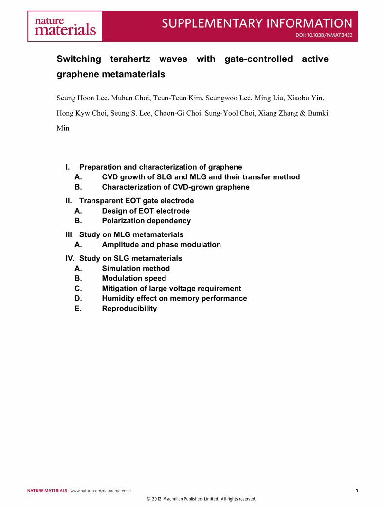
expressions are given here; ����eff � � ������ and ����eff � ����
�� , where ���� and ���� are the real and
imaginary part of complex conductivity of graphene, � is the angular frequency, and � is
the thickness of graphene. Here, � is not the actual thickness of graphene and it is
sufficient to choose the value of � much smaller than the wavelength of interest for the
simulation. The complex permittivity of graphene is shown in Fig. S8. The plots are
generated by assuming the thickness of graphene � = 1 nm and the intraband scattering
time of � = 16 fs.
Figure S8 | Complex permittivity of graphene used in the simulation of the active graphene metamaterials a, Real and b, imaginary part of the effective permittivity
14 NATURE MATERIALS | www.nature.com/naturematerials
SUPPLEMENTARY INFORMATION DOI: 10.1038/NMAT3433
© 2012 Macmillan Publishers Limited. All rights reserved.

15
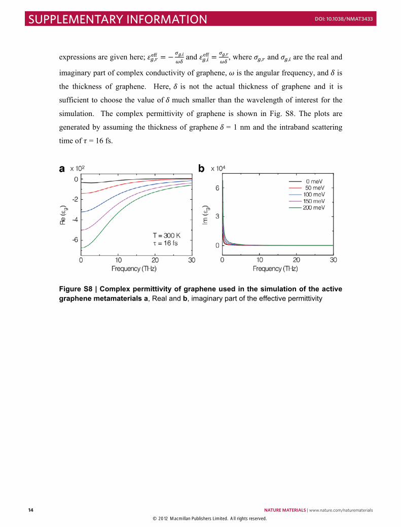
B. Modulation speed
In order to estimate the modulation speed of our devices, we have applied ac rectangular
voltage (0 – 10 V) simultaneously to the gate of the active metamaterial and the terahertz
emitter while sweeping the frequency of modulation from 1 to 100 kHz, as with the
method used in the previous studies of THz modulators [11, 12] (For our THz-TDS setup,
the highest frequency response that can be measured is limited to ~100 kHz, which is due
to the limited frequency response of the constituting components, such as the terahertz
emitter and the lock-in amplifier). Figure S9a shows the time-domain waveforms with
(bottom) and without (top) the active graphene metamaterials for the modulating
frequencies of 1, 50, and 100 kHz, respectively. As can be clearly seen from the plots,
the shape of the waveforms was not significantly altered with a variation in modulation
frequency. The peak-to-peak THz wave signal transmitted through the sample (i.e.,
active graphene metamaterial) is normalized to the reference signal (measured without
the sample) at each modulation frequency, and these normalized values are recorded as a
function of the modulation frequency (black circles in Fig. S9b). Up to 100 kHz, the
frequency response roll-off was not obviously observed in the frequency response. Thus,
we can conclude that the modulation speed of the proposed active graphene metamaterial
exceeds at least 100 kHz.
In order to make up for the limited response range that can be measured with THz-TDS
setup, we have measured the dynamic response (S21) of the device using a radio
frequency (r.f.) network analyser. Figure S9c shows a frequency dependent response of
the graphene metamaterial. With the RC time constant fitting, the 3-dB roll-off frequency
of the device was estimated to be 12.6 MHz, the value of which is comparable to those of
2DEG-based high speed terahertz modulators with metamaterials (~10 MHz) [13]. From
these results, we established that the operating bandwidth is not limited by the carrier
transit time in graphene layer, but by the parasitic response of the device.
NATURE MATERIALS | www.nature.com/naturematerials 15
SUPPLEMENTARY INFORMATIONDOI: 10.1038/NMAT3433
© 2012 Macmillan Publishers Limited. All rights reserved.
16
Figure S9 | Transmitted terahertz waves with and without the gate-controlled active graphene metamaterials and its frequency response measured by THz-TDS and network analyser a, The transmitted terahertz wave signals with and without the gate-controlled active graphene metamaterials for modulation frequencies of 1, 50, and 100 kHz. b, The frequency response of the graphene metamaterials as a function of modulation frequency (black circle). c, Frequency response of the graphene metamaterials measured by r.f. network analyser (black square). The modulation speed is limited by RC time constant of the device. The RC time constant fitting (red curve) shows that 3-dB roll-off frequency for the graphene metamaterial (spacing ~2 μm) is 12.6 MHz.
16 NATURE MATERIALS | www.nature.com/naturematerials
SUPPLEMENTARY INFORMATION DOI: 10.1038/NMAT3433
© 2012 Macmillan Publishers Limited. All rights reserved.

17
C. Mitigation of large voltage requirement
The maximum gate voltage applied to our graphene metamaterials (presented in the main
manuscript) was on the order of a few hundred volts (for devices with dielectric spacing
of ~2 μm). However, the required gate voltage can be reduced simply by decreasing the
dielectric (here, polyimide layer) spacing (d) between the EOT gate electrode and the
graphene layer. As mentioned in the main manuscript, the EOT gate capacitance in the
electron charge is estimated to be α = 8.54 × 109 cm-2V-1. This value is approximately an
order of magnitude smaller than previously reported value [14], for which the dielectric
spacing d between graphene and back-gate was ~300 nm.
A simple electrostatic parallel capacitor model can be adapted to provide the required
voltage dependence on the spacing of dielectric layer. The total number of charge
carriers accumulated in the proposed EOT gate (or graphene layer) can be expressed as:
�� � ��� � ������ � ����� � �����|��|�����, where q is the elementary charge, �� is
the relative permittivity of dielectric (polyimide), �� is the permittivity of free space, and
A is the area of graphene layer. By defining the EOT gate capacitance in the electron
charge � � ���������, we can obtain the gate-voltage dependent charge (hole) density in
the graphene layer as follows,
�� � ���� �
������ �� � ������ � ���
where VCNP is the charge neutral gate voltage in our device. As seen from above equation,
the rate of change in charge density with respect to the gate voltage (��� ���⁄ � � �) is the
EOT gate capacitance in the electron charge. Thus, one of the easiest ways to obtain a
high proportional constant � could be to reduce the dielectric spacing d.
As a proof of concept, we have fabricated active graphene metamaterials with two
different dielectric spacing and measured the rate of change of transmission with a
variation in gate voltage for these two sets of samples. The thickness of dielectric
spacing could be precisely controlled both by the spin-coating speed and by the
polyimide solution. Two sets of newly fabricated samples were designed to have
NATURE MATERIALS | www.nature.com/naturematerials 17
SUPPLEMENTARY INFORMATIONDOI: 10.1038/NMAT3433
© 2012 Macmillan Publishers Limited. All rights reserved.

18
dielectric spacing distance d of 1 and 2 μm, respectively. Figure S10 shows the gate
voltage dependent transmission spectra and its relative change as a function of dielectric
spacing for these two samples. For comparison, the relative changes in transmission at
resonance frequency for two samples are plotted as a function of Vg in Fig. S10e. As
seen from the plot, the sample with 2-μm-thick spacing needs approximately two times
larger gate voltage than that with 1-μm-thick spacing to achieve a comparable change of
transmission. This result confirms that the required voltage can be effectively reduced by
decreasing the dielectric spacing between the EOT electrodes and the graphene layer.
18 NATURE MATERIALS | www.nature.com/naturematerials
SUPPLEMENTARY INFORMATION DOI: 10.1038/NMAT3433
© 2012 Macmillan Publishers Limited. All rights reserved.

19
Figure S10 | Gate voltage dependent transmission spectra and its relative change as a function of dielectric spacing a and b for 2 μm spacing; c and d for 1 μm spacing. e, Relative change in transmission at resonance frequency plotted as a function of Vg for samples with two different dielectric spacing. The sample with 2-μm-thick spacing needs approximately two times larger gate voltage than that with 1-μm-thick spacing sample.
NATURE MATERIALS | www.nature.com/naturematerials 19
SUPPLEMENTARY INFORMATIONDOI: 10.1038/NMAT3433
© 2012 Macmillan Publishers Limited. All rights reserved.

20
D. Humidity effect on memory performance
In the main manuscript, we attributed one of the possible origins of hysteretic behaviour
in transmission to the adsorption/desorption process of H2O molecules. Although the
graphene layer in our device is partially protected from the air by the encapsulation of PI
(see schematic of device architecture), H2O molecules can still reach and adsorb onto the
graphene layer. This is because H2O molecules are able to penetrate into the PI layer
covering the graphene [15]. In order to clarify the effect of H2O adsorption, we have
carried out measurement under a controlled humidity environment. First, we recorded
the binary memory operation of active graphene metamaterial held in dry air (humidity of
~0.5%) and the results are shown in Fig. S11a. Prior to the measurement, the sample
under test was put in dry air chamber (humidity of ~0.5%) for 24 hours. As mentioned in
the main manuscript, the measured retention time is a function of applied gate voltage
and doping time. Here, for this measurement, the doping time and peak voltage are set to
60 seconds and 300 V gate voltages, respectively. The measured memory retention time
was found to be ~30 minutes and its decay time was estimated to be ~23 minutes. For
comparison, the identical sample was exposed to a highly humid environment (humidity
of ~70%) for 3 hours and the measurement was performed to estimate the retention time
and decay constant. Interestingly, the measured retention time of the sample held in
highly humid condition was approximately two times larger than that of the sample held
in dry air. The decay time was around 46 minutes as can be confirmed in Fig. S11b.
From these controlled experiments, we can conclude that the water adsorption plays a
pivotal role in memory retention time and decay time.
20 NATURE MATERIALS | www.nature.com/naturematerials
SUPPLEMENTARY INFORMATION DOI: 10.1038/NMAT3433
© 2012 Macmillan Publishers Limited. All rights reserved.

21
Figure S11 | Effect of humidity on the memory operation Binary memory operation in transmission near resonance (top panel) with gating pulse signal of 300 V (low panel) for the same sample measured a, in a dry air condition (humidity of ~0.5%) and b, after putting the samples in ~70% humidity for 3 hours. The measured memory retention time before and after the water adsorption is about ~30 and ~60 minutes, respectively. Owing to considerable water adsorption, decay constant of 70%-humidity-sample is also increased to be 46 minutes from sample in dry air of 23 minutes.
NATURE MATERIALS | www.nature.com/naturematerials 21
SUPPLEMENTARY INFORMATIONDOI: 10.1038/NMAT3433
© 2012 Macmillan Publishers Limited. All rights reserved.

22
E. Reproducibility
To check the reproducibility of hysteretic behaviour in gate-controlled transmission and
the photonic memory operation, we have fabricated three devices with the same
architecture (Fig. 1a in main manuscript). Three devices were constructed simultaneously
onto a single 4-inch silicon wafer. Arbitrary chosen parts of CVD-grown graphene (on
80 80 mm2 Cu foil) were transferred to three lithographically identical devices (parts
being shown in Fig. S12a). Finally, all samples were soldered to drilled PBC substrates
(Fig. S12b). We summarized in this response the results for three devices labelled as #1,
#2, and #3. First, the resonance frequencies for three devices are nearly the same, as can
be seen in Fig. S12c. The observation of nearly identical resonance frequencies indicates
that the structural fidelity of metamaterials (e.g., sizes, widths, gaps of meta-atoms) was
reproducible across three devices on a single wafer. However, for the hysteretic
behaviour in gate-controlled transmission (Fig. S12d) and the photonic memory operation
(Fig. S12e), while quite a similar trend is observed, they are not perfectly identical across
the three devices. This sample-to-sample variation in a single batch can be attributed to
the spatial variations (of defects and doping) of CVD-grown graphene. Even with the
state-of-the-art preparation of CVD-grown graphene, such variables seem to be
unavoidable at the current stage [16], and further improvements in the production of
CVD-graphene would be required to guarantee the complete reproducibility of the gate-
controlled active graphene metamaterials.
22 NATURE MATERIALS | www.nature.com/naturematerials
SUPPLEMENTARY INFORMATION DOI: 10.1038/NMAT3433
© 2012 Macmillan Publishers Limited. All rights reserved.

23
Figure S12 | Reproducibility test for the gate-controlled active graphene metamaterial a, large area CVD-grown graphene on Cu foil (80 × 80 mm2) purchased from GRAPHENE SQUARE. The parts designated with numbers represent the graphene used in the fabrication. b, All samples were soldered to drilled PBC substrates. c, Measured relative change in transmission with respect to the gate voltage of 80 V, d, hysteretic on-resonance transmission, e, binary memory operation of the three samples.
NATURE MATERIALS | www.nature.com/naturematerials 23
SUPPLEMENTARY INFORMATIONDOI: 10.1038/NMAT3433
© 2012 Macmillan Publishers Limited. All rights reserved.

24
References
[1] A. C. Ferrari, J. C. Meyer, V. Scardaci, C. Casiraghi, M. Lazzeri, F. Mauri, S. Piscanec, D. Jiang, K. S. Novoselov, S. Roth, and A. K. Geim, "Raman Spectrum of Graphene and Graphene Layers," Physical Review Letters, vol. 97, p. 187401, 2006.
[2] D. M. Basko, S. Piscanec, and A. C. Ferrari, "Electron-electron interactions and doping dependence of the two-phonon Raman intensity in graphene," Physical Review B, vol. 80, p. 165413, 2009.
[3] A. Das, S. Pisana, B. Chakraborty, S. Piscanec, S. K. Saha, U. V. Waghmare, K. S. Novoselov, H. R. Krishnamurthy, A. K. Geim, A. C. Ferrari, and A. K. Sood, "Monitoring dopants by Raman scattering in an electrochemically top-gated graphene transistor," Nat Nano, vol. 3, pp. 210-215, 2008.
[4] L. G. Cançado, A. Jorio, E. H. M. Ferreira, F. Stavale, C. A. Achete, R. B. Capaz, M. V. O. Moutinho, A. Lombardo, T. S. Kulmala, and A. C. Ferrari, "Quantifying Defects in Graphene via Raman Spectroscopy at Different Excitation Energies," Nano Letters, vol. 11, pp. 3190-3196, 2011.
[5] T. W. Ebbesen, H. J. Lezec, H. F. Ghaemi, T. Thio, and P. A. Wolff, "Extraordinary optical transmission through sub-wavelength hole arrays," Nature, vol. 391, pp. 667-669, 1998.
[6] M. A. Ordal, L. L. Long, R. J. Bell, S. E. Bell, R. R. Bell, J. R. W. Alexander, and C. A. Ward, "Optical properties of the metals Al, Co, Cu, Au, Fe, Pb, Ni, Pd, Pt, Ag, Ti, and W in the infrared and far infrared," Appl. Opt., vol. 22, pp. 1099-1119, 1983.
[7] M. Choi, S. H. Lee, Y. Kim, S. B. Kang, J. Shin, M. H. Kwak, K.-Y. Kang, Y.-H. Lee, N. Park, and B. Min, "A terahertz metamaterial with unnaturally high refractive index," Nature, vol. 470, pp. 369-373, 2011.
[8] V. P. Gusynin, S. G. Sharapov, and J. Carbotte, "Ac conductivity of graphene: From tight-binding model to 2+1-dimension electrodynamics," International Journal of Modern Physics B, vol. 21, pp. 4611-4658, Oct 30 2007.
[9] R. Saito, G. Dresselhaus, and S. Dresselhaus, Physical Properties of Carbon Nanotubes: Imperial College Press, 1998.
[10] A. Vakil and N. Engheta, "Transformation Optics Using Graphene," Science, vol. 332, pp. 1291-1294, Jun 10 2011.
[11] H. T. Chen, W. J. Padilla, J. M. O. Zide, A. C. Gossard, A. J. Taylor, and R. D. Averitt, "Active terahertz metamaterial devices," Nature, vol. 444, pp. 597-600, Nov 30 2006.
[12] H. T. Chen, S. Palit, T. Tyler, C. M. Bingham, J. M. O. Zide, J. F. O'Hara, D. R. Smith, A. C. Gossard, R. D. Averitt, W. J. Padilla, N. M. Jokerst, and A. J. Taylor, "Hybrid metamaterials enable fast electrical modulation of freely propagating terahertz waves," Applied Physics Letters, vol. 93, p. 091117, Sep 1 2008.
[13] D. Shrekenhamer, S. Rout, A. C. Strikwerda, C. Bingham, R. D. Averitt, S. Sonkusale, and W. J. Padilla, "High speed terahertz modulation from
24 NATURE MATERIALS | www.nature.com/naturematerials
SUPPLEMENTARY INFORMATION DOI: 10.1038/NMAT3433
© 2012 Macmillan Publishers Limited. All rights reserved.
25
metamaterials with embedded high electron mobility transistors," Optics Express, vol. 19, pp. 9968-9975, May 9 2011.
[14] F. Wang, Y. B. Zhang, C. S. Tian, C. Girit, A. Zettl, M. Crommie, and Y. R. Shen, "Gate-variable optical transitions in graphene," Science, vol. 320, pp. 206-209, Apr 11 2008.
[15] J. Seo and H. Han, "Water sorption behaviour of polyimide thin films with various internal linkages in the dianhydride component," Polymer Degradation and Stability, vol. 77, pp. 477-482, 2002.
[16] K. S. Kim, Y. Zhao, H. Jang, S. Y. Lee, J. M. Kim, K. S. Kim, J.-H. Ahn, P. Kim, J.-Y. Choi, and B. H. Hong, "Large-scale pattern growth of graphene films for stretchable transparent electrodes," Nature, vol. 457, pp. 706-710, 2009.
NATURE MATERIALS | www.nature.com/naturematerials 25
SUPPLEMENTARY INFORMATIONDOI: 10.1038/NMAT3433
© 2012 Macmillan Publishers Limited. All rights reserved.