
Suitability of nanodiamond nitrogen–vacancy centers for
25
PAPER • OPEN ACCESS Suitability of nanodiamond nitrogen–vacancy centers for spontaneous emission control experiments To cite this article: Abbas Mohtashami and A Femius Koenderink 2013 New J. Phys. 15 043017 View the article online for updates and enhancements. You may also like Charge state stabilization of shallow nitrogen vacancy centers in diamond by oxygen surface modification Hayate Yamano, Sora Kawai, Kanami Kato et al. - Screening and engineering of colour centres in diamond Tobias Lühmann, Nicole Raatz, Roger John et al. - Magnetometry with nitrogen-vacancy defects in diamond L Rondin, J-P Tetienne, T Hingant et al. - Recent citations Decay rate enhancement of diamond NV- centers on diamond thin films Hao Li et al - On Quantum Efficiency Measurements and Plasmonic Antennas Korenobu Matsuzaki et al - Hyperbolic metamaterial-based metal–dielectric resonator-antenna designs for GHz photon collection rates from wide-range solid-state single-photon sources Nadeem Ahmed et al - This content was downloaded from IP address 45.172.99.236 on 01/12/2021 at 06:13
Transcript of Suitability of nanodiamond nitrogen–vacancy centers for

PAPER • OPEN ACCESS
Suitability of nanodiamond nitrogen–vacancycenters for spontaneous emission controlexperimentsTo cite this article: Abbas Mohtashami and A Femius Koenderink 2013 New J. Phys. 15 043017
View the article online for updates and enhancements.
You may also likeCharge state stabilization of shallownitrogen vacancy centers in diamond byoxygen surface modificationHayate Yamano, Sora Kawai, KanamiKato et al.
-
Screening and engineering of colourcentres in diamondTobias Lühmann, Nicole Raatz, RogerJohn et al.
-
Magnetometry with nitrogen-vacancydefects in diamondL Rondin, J-P Tetienne, T Hingant et al.
-
Recent citationsDecay rate enhancement of diamond NV-centers on diamond thin filmsHao Li et al
-
On Quantum Efficiency Measurementsand Plasmonic AntennasKorenobu Matsuzaki et al
-
Hyperbolic metamaterial-basedmetal–dielectric resonator-antennadesigns for GHz photon collection ratesfrom wide-range solid-state single-photonsourcesNadeem Ahmed et al
-
This content was downloaded from IP address 45.172.99.236 on 01/12/2021 at 06:13
Suitability of nanodiamond nitrogen–vacancy centersfor spontaneous emission control experiments
Abbas Mohtashami1 and A Femius KoenderinkCenter for Nanophotonics, FOM Institute for Atomic and Molecular Physics(AMOLF), Science Park 104, 1098-XG Amsterdam, The NetherlandsE-mail: [email protected]
New Journal of Physics 15 (2013) 043017 (24pp)Received 20 December 2012Published 15 April 2013Online at http://www.njp.org/doi:10.1088/1367-2630/15/4/043017
Abstract. Nitrogen–vacancy (NV) centers in diamond are generally recog-nized as highly promising as indefinitely stable highly efficient single-photonsources. We report an experimental quantification of the brightness, radiativedecay rate, nonradiative decay rate and quantum efficiency of single NV centersin diamond nanocrystals. Our experiments show that the commonly observedlarge spread in fluorescence decay rates of NV centers in nanodiamond is incon-sistent with the common explanation of large nanophotonic mode-density varia-tions in the ultra-small high-index crystals at near-unity quantum efficiency. Wereport that NV centers in 25 nm nanocrystals are essentially insensitive to localdensity of optical states (LDOS) variations that we induce at a dielectric interfaceby using liquids to vary the refractive index, and propose that quantum efficien-cies in such nanocrystals are widely distributed between 0 and 20%. For singleNV centers in larger 100 nm nanocrystals, we show that decay rate changes canbe reversibly induced by nanomechanically approaching a mirror to change theLDOS. Using this scanning mirror method, for the first time we report calibratedquantum efficiencies of NV centers, and show that different but nominally iden-tical nanocrystals have widely distributed quantum efficiencies between 10 and90%. Our measurements imply that nanocrystals that are to be assembled intohybrid photonic structures for cavity QED should first be individually screenedto assess fluorescence properties in detail.
1 Author to whom any correspondence should be addressed.
Content from this work may be used under the terms of the Creative Commons Attribution 3.0 licence.Any further distribution of this work must maintain attribution to the author(s) and the title of the work, journal
citation and DOI.
New Journal of Physics 15 (2013) 0430171367-2630/13/043017+24$33.00 © IOP Publishing Ltd and Deutsche Physikalische Gesellschaft
2
Contents
1. Introduction 22. Experiment and methods 4
2.1. Sample preparation . . . . . . . . . . . . . . . . . . . . . . . . . . . . . . . . 42.2. Experimental setup . . . . . . . . . . . . . . . . . . . . . . . . . . . . . . . . 52.3. Measurement procedure to characterize single nanodiamonds . . . . . . . . . . 6
3. Statistics on fluorescence parameters of large nanodiamonds 83.1. Distribution of brightness and relation to g(2)(0) . . . . . . . . . . . . . . . . . 83.2. Correlation of emission rates and brightness . . . . . . . . . . . . . . . . . . . 103.3. Common local density of optical states (LDOS) argument for rate variation in
nanodiamonds . . . . . . . . . . . . . . . . . . . . . . . . . . . . . . . . . . . 103.4. LDOS argument beyond unit quantum efficiency . . . . . . . . . . . . . . . . 11
4. Statistics on small nanodiamonds 124.1. Brightness and g(2)(0) . . . . . . . . . . . . . . . . . . . . . . . . . . . . . . . 124.2. Distribution of rates . . . . . . . . . . . . . . . . . . . . . . . . . . . . . . . . 124.3. Comparison with the LDOS argument for distribution of rates . . . . . . . . . 13
5. LDOS tuning on single nitrogen–vacancy (NV) centers 145.1. Liquid tuning of LDOS on single NV centers in small nanodiamonds . . . . . . 155.2. Nanomechanical tuning of LDOS on large nanodiamonds . . . . . . . . . . . . 17
6. Conclusion 20Acknowledgments 22References 22
1. Introduction
The great promise of quantum-optical technologies to enable secure communication and novelcomputation architectures sets stringent targets for the quality of photon sources and detectors.In order to meet these demands, many efforts are currently devoted to realizing bright sourcesof single photons [1, 2]. These developments at the same time require novel nanophotonicengineering designs around emitters to enhance light–matter interaction strength as well asindefinitely stable two-level systems that neither bleach, blink nor spectrally jump. On thenanophotonic engineering side, many different systems have been proposed to control whereto,how fast and with which polarization an emitter emits provided that one manages to locateit exactly in the right location. These systems include whispering-gallery-mode cavities [2],micropillars and cylindrical wires [3–5], photonic-crystal microcavities [6–8], photonic-crystalwaveguides near cut-off [9, 10], Anderson localizing systems [11], as well as ultrabroadbandplasmonic waveguides and antennas [12–15]. Essentially, all these techniques modify thephotonic environment of an emitter via the local density of optical states (LDOS) [16, 17].The LDOS quantifies the light–matter interaction strength that appears in Fermi’s golden rulefor spontaneous emission. Placing the emitter at a position where the LDOS is enhanced firstlyimplies a much higher fluorescence decay rate. Secondly, if the LDOS enhancement is due toa select set of designed modes as in a cavity or waveguide, the enhanced rate is accompaniedby extraction of photons preferentially via these enhanced modes. Thus, photonic engineering
New Journal of Physics 15 (2013) 043017 (http://www.njp.org/)
3
promises optimum brightness, dynamics and collection efficiency. As regards the choice of theemitter, a wide variety of systems has been used. Unfortunately, all choices appear to carrylarge disadvantages when going beyond pilot studies: most dye molecules photobleach [18],II–VI quantum dots [19, 20] blink as well as bleach, and many systems, such as III–Vemitters, only have desirable properties when cooled to cryogenic temperatures [3–7, 10, 11].A promising candidate to provide an indefinitely stable source [21–23] that furthermore allowsroom-temperature spin control [24–28] is the nitrogen–vacancy (NV) color center in diamond.Offsetting their advantageous stability, a disadvantage of NV centers as single-photon sourcesis their very broadband fluorescence emission compared to other quantum emitters at roomtemperature, which makes frequency-selective photonic engineering challenging.
When one chooses diamond NV centers as emitters for quantum optics in nanophotonicdevices, one can either aim to manipulate emission by fabricating photonic structures directlyin diamond [29–31], or one can assemble diamond nanocrystals with photonic structures of adifferent material [32–39]. Recently, pick-and-place strategies [35–37] were reported in whicha single nanoparticle from a diluted powder of diamond nanocrystals dispersed on a substrateis selected and pushed to a desired location by a scanning probe, such as an atomic-force-microscopy tip, or a manipulator in a scanning electron microscope (SEM). Reports of thistechnique span from the coupling of nanodiamonds to photonic-crystal cavities [36, 37] tocoupling to plasmonic antennas and nanowires [38, 39]. As a variation of the pick-and-placestrategy, a few groups recently developed so-called ‘scanning-emitter’ near-field microscopesin which nanosources are not deposited irreversibly inside a nanostructure, but actually remainattached to a scanning probe [40–43]. The advantage of such a scanning-probe approach isthat one can first construct a full map of the LDOS using near-field lifetime imaging todetermine where one should ultimately place the nanosource [43]. Microscopy with a lightsource as a near-field tip is interesting as a microscopy technique, but only viable if thenanosource is indefinitely stable and does not blink, for which nanodiamonds appear to be thesole candidate [41, 42]. Moreover, nanodiamond scanning probes offer the possibility to createnanometer-sized local magnetometry probes read out optically by NV spectroscopy [44–47].
In view of the scanning probe microscopy and assembly efforts that seek to combinenanodiamonds and photonic structures, one question stands out as of key importance: givenan ensemble of individual nanodiamonds, how does one recognize the ideal nanocrystal? Thisquestion is especially relevant given that both fabrication of the photonic structure and theintended scanning-probe procedure are highly laborious [35]. Naively, one might think thatall nanocrystals of subwavelength size that contain a single NV center will be equally suited,since an NV center is a defect of uniquely defined composition and geometry in the diamondcrystalline matrix. However, many workers on diamond nanocrystals have established that NVcenters in diamond nanocrystals actually show a distribution of photophysical properties, suchas brightness, stability and decay rates [28, 36, 48–51]. This distribution is usually ascribed tothe fact that even though all NV centers are expected to have unit quantum efficiency and thesame oscillator strength, these identical unit-quantum-efficiency sources are each differentlyplaced inside their nanoscopic high-index diamond grains [21–23, 49, 51]. This is anticipated tocause different decay rates, due to the fact that the LDOS even in an isolated nanoscopic objectvaries as a function of position and dipole orientation [52].
In this paper we address the question of how to recognize the ideal nanocrystal froman ensemble of nanocrystals on the basis of the requirement that the ideal nanocrystal mustcontain a single NV− center that fluoresces with a high quantum yield, so that it can be
New Journal of Physics 15 (2013) 043017 (http://www.njp.org/)
4
useful as a reporting probe of LDOS in nanophotonic systems. We report that the commonlymade assumption that NV centers are unit-efficiency dipoles randomly distributed in high-indexnanoscopic objects is not reconcilable with measured brightness and decay rate histograms datafor nanocrystals in the frequently used size ranges around 20–50 and 50–150 nm. On the basisof the wide distribution of brightness and rate that cannot be explained by LDOS variationsbetween nanoparticles alone, we conclude that both the radiative and nonradiative rates arebroadly distributed. To quantify this distribution, we have performed experiments in which wemeasure emission rate changes of individual nanodiamonds as we controllably vary the LDOSof their environment. For small nanocrystals we find a decay rate distribution indicative of low-quantum-efficiency emitters. Furthermore, consistent with this low quantum efficiency, we findno evidence that small single NV centers are responsive LDOS probes when applying moderateLDOS variations. For the larger nanocrystals (100 nm diameter), we for the first time manageto induce reversible changes of up to 25% in the total decay rate of single NV centers using acalibrated LDOS change induced by a nanomechanically moved mirror. On the basis of thesemeasurements, we argue that the apparent quantum efficiency of nanodiamonds in the size rangeof 50–150 nm ranges widely from about 10 to 90%. This wide range of quantum efficienciesimplies that prior to constructing a photonic structure, it is necessary to screen the nanocrystalsusing a calibrated quantum-efficiency measurement on the single NV center level, as shown inthis paper. This paper is organized in the following manner. First we report on our experimentalmethods in section 2. Next, we discuss the distributions of brightnesses and rates for largenanocrystals in section 3 and for small nanocrystals in section 4. Finally, we report on effortsto tune rates of NV centers in small diamonds by controlled LDOS changes. The two methodsused are liquid tuning of LDOS in section 5.1, and nanomechanically approaching a mirror asreported in section 5.2.
2. Experiment and methods
2.1. Sample preparation
Since single NV centers in nanodiamonds are comparatively dim emitters that requirehigh excitation powers, it is essential to avoid background fluorescence when performingfluorescence microscopy. Therefore, we use intrinsically low-fluorescent quartz coverslips(Esco Products) as sample substrates that were cleaned by 15 min sonication in water followedby a 15 min bath in base Piranha (NH3(aq., 30%) : H2O2(aq., 30%) : H2O mixed at ratio 1 : 1 : 5,at 75 ◦C). In our work it is essential that we can unambiguously pinpoint the position ofnanodiamonds containing NV centers in the course of the measurement, so that we can revisitthe same color center after, for instance, material-deposition steps. To this end, we define anarray of markers on top of the coverslips using electron-beam lithography. To remove anyorganic residues after the lift-off process, we treated the coverslips with a mild O2-plasmadescum (Oxford Instruments Plasmalab 80+, using a 5 mTorr, 25 sccm O2 plasma). As sourcesfor NV centers, we use solutions of monocrystalline synthetic nanodiamonds (MicrodiamantMSY) with a narrow size tolerance obtained from Microdiamant AG, Lengwil, Switzerland. Wenote that these nanoparticles have been used recently by a large number of groups in experimentsthat rely on fluorescence [26, 27, 32, 36, 38, 39, 48–50]. We use these nanodiamonds exactlyin the manner as described by Schietinger et al, i.e. without further washing or purificationsteps [36, 53]. We prepared samples from diamond slurries with two different size distributions
New Journal of Physics 15 (2013) 043017 (http://www.njp.org/)

5
by spin-coating aqueous solutions of nanodiamonds that are diluted to a concentration of 1% ofthe as-received stock solutions on the cleaned and patterned coverslips. The first type of sample,from here on referred to as ‘25 nm diamond sample’, was made from Microdiamant MSY0–0.05, which nominally has sizes from 0 to 50 nm. These diamonds have a median diameterof 26 nm, with fewer than 1% of the diamonds above 50 nm in size, according to particle sizingperformed on this batch of diamonds by the manufacturer. The second type of sample (‘100 nmdiamond sample’) was made from Microdiamant MSY 0–0.2, which nominally has crystal sizesranging from 0 to 200 nm. This ensemble has crystals with median diameter 108 nm, and fewerthan 1% of particles above 175 nm in size, again according to the size-distribution histogramsupplied by the manufacturer. SEM inspection indicated a size distribution of nanodiamondsconsistent with these specifications. The average density of spin-coated nanodiamonds on thecoverslips as checked through the SEM images was about 1–8 µm−2 depending on the sample,ensuring that only a few nanodiamonds are illuminated at the diffraction-limited focus ofthe objective. Only a small fraction of the nanodiamonds is fluorescent, and an even smallerfraction fluoresces due to an NV center. We identify a diamond as containing at least one NVcenter, if we can clearly identify the characteristic zero phonon line (ZPL) [21–23, 54] in itsemission spectrum according to the criterion we specify in section 2.3. With this criterion,for 100 nm nanodiamonds at an average density of 1 µm−2, we found on average one NVcenter in an area equal to 50 × 50 µm2, while for 25 nm nanodiamonds at an average densityof 5 µm−2 we found on average two NV centers in a 100 × 100 µm2 area. These numberstranslate to identifying fewer than 0.05% of the 100 nm nanodiamonds, and fewer than 0.001%of the 25 nm diamonds as containing a single NV center beyond doubt. Schietinger et al [55]have reported a higher density of NV centers of about 1% for MSY 0–0.05 nanodiamonds.A difference in reported NV center densities could be either due to a different degree ofstrictness in labeling a fluorescent emitter as an NV center beyond doubt (see section 2.3 forour criteria), or alternatively due to batch-to-batch variations in nanodiamond slurries.
2.2. Experimental setup
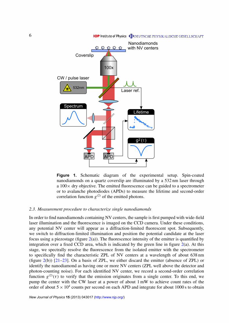
The optical setup, sketched in figure 1, consists of an inverted confocal fluorescence microscopeequipped with a sample scanning piezostage. NV centers are optically excited at 532 nm usingeither a frequency-doubled Nd : YAG pulsed laser (Time-Bandwidth, 10 MHz repetition rate) ora continuous-wave (CW) diode laser (CNI). The laser beam is focused through the coverslip toa diffraction-limited spot on top of the sample, using a 100× dry objective with a numericalaperture of 0.9 (Nikon CFI Plan Fluor). The same objective collects the luminescence andguides it through a long-pass filter (580 nm cut-off) before it is imaged on a charge-coupleddevice (CCD) camera (Nikon DS-Qi1Mc) or confocally detected on one or two avalanchephotodiodes (APDs) with single-photon sensitivity (both APDs: id Quantique id100-20ULN).The APDs in combination with a sub-nanosecond-resolution 16-channel correlator (Becker &Hickl, DPC-230) allow for single-photon counting. The correlator can perform time-correlatedsingle-photon-counting lifetime measurements by correlation of detection events with laserpulse arrival times, or photon–photon correlations using multiple APDs. We use a secondAPD in a Hanbury-Brown and Twiss configuration to measure photon correlation statistics(antibunching) at CW excitation. Single-nanocrystal spectra are collected using an imagingspectrometer (SpectraPro 2300i) equipped with a thermoelectrically cooled back-illuminatedSi CCD array detector (Princeton Instruments PIXIS:100B).
New Journal of Physics 15 (2013) 043017 (http://www.njp.org/)
6
Figure 1. Schematic diagram of the experimental setup. Spin-coatednanodiamonds on a quartz coverslip are illuminated by a 532 nm laser througha 100× dry objective. The emitted fluorescence can be guided to a spectrometeror to avalanche photodiodes (APDs) to measure the lifetime and second-ordercorrelation function g(2) of the emitted photons.
2.3. Measurement procedure to characterize single nanodiamonds
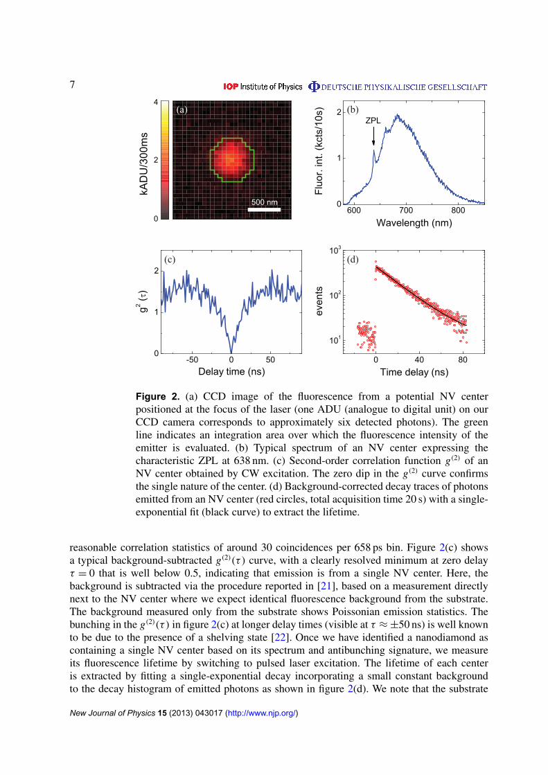
In order to find nanodiamonds containing NV centers, the sample is first pumped with wide-fieldlaser illumination and the fluorescence is imaged on the CCD camera. Under these conditions,any potential NV center will appear as a diffraction-limited fluorescent spot. Subsequently,we switch to diffraction-limited illumination and position the potential candidate at the laserfocus using a piezostage (figure 2(a)). The fluorescence intensity of the emitter is quantified byintegration over a fixed CCD area, which is indicated by the green line in figure 2(a). At thisstage, we spectrally resolve the fluorescence from the isolated emitter with the spectrometerto specifically find the characteristic ZPL of NV centers at a wavelength of about 638 nm(figure 2(b)) [21–23]. On a basis of ZPL, we either discard the emitter (absence of ZPL) oridentify the nanodiamond as having one or more NV centers (ZPL well above the detector andphoton-counting noise). For each identified NV center, we record a second-order correlationfunction g(2)(τ ) to verify that the emission originates from a single center. To this end, wepump the center with the CW laser at a power of about 1 mW to achieve count rates of theorder of about 5 × 10⁴ counts per second on each APD and integrate for about 1000 s to obtain
New Journal of Physics 15 (2013) 043017 (http://www.njp.org/)
7
Figure 2. (a) CCD image of the fluorescence from a potential NV centerpositioned at the focus of the laser (one ADU (analogue to digital unit) on ourCCD camera corresponds to approximately six detected photons). The greenline indicates an integration area over which the fluorescence intensity of theemitter is evaluated. (b) Typical spectrum of an NV center expressing thecharacteristic ZPL at 638 nm. (c) Second-order correlation function g(2) of anNV center obtained by CW excitation. The zero dip in the g(2) curve confirmsthe single nature of the center. (d) Background-corrected decay traces of photonsemitted from an NV center (red circles, total acquisition time 20 s) with a single-exponential fit (black curve) to extract the lifetime.
reasonable correlation statistics of around 30 coincidences per 658 ps bin. Figure 2(c) showsa typical background-subtracted g(2)(τ ) curve, with a clearly resolved minimum at zero delayτ = 0 that is well below 0.5, indicating that emission is from a single NV center. Here, thebackground is subtracted via the procedure reported in [21], based on a measurement directlynext to the NV center where we expect identical fluorescence background from the substrate.The background measured only from the substrate shows Poissonian emission statistics. Thebunching in the g(2)(τ ) in figure 2(c) at longer delay times (visible at τ ≈ ±50 ns) is well knownto be due to the presence of a shelving state [22]. Once we have identified a nanodiamond ascontaining a single NV center based on its spectrum and antibunching signature, we measureits fluorescence lifetime by switching to pulsed laser excitation. The lifetime of each centeris extracted by fitting a single-exponential decay incorporating a small constant backgroundto the decay histogram of emitted photons as shown in figure 2(d). We note that the substrate
New Journal of Physics 15 (2013) 043017 (http://www.njp.org/)

8
itself has a weak background fluorescence that shows time dependence. We correct for thisartifact by collecting decay traces from the sample pumped directly next to the NV center. Weparameterize the background by a tri-exponential fit (with a dominant sub-nanosecond lifetime),which we subtract from the NV center decay histogram prior to fitting. The residual backgroundis around 10 counts per bin for a total acquisition time of about 20 s.
3. Statistics on fluorescence parameters of large nanodiamonds
In this section we report on statistical distributions of the various fluorescence characteristics,i.e. brightness, g(2) and lifetime, that we collected on both nanodiamond size ranges. We firstdiscuss the ‘100 nm diamond’ sample, containing 0–200 nm size nanodiamonds with 108 nmmedian diameter, and subsequently we discuss the ‘25 nm diamond’ sample with 0–50 nmsize nanodiamonds and 26 nm median diameter. For each sample, our statistics is based onidentifying 30–40 NV centers as described in section 2.3.
3.1. Distribution of brightness and relation to g(2)(0)
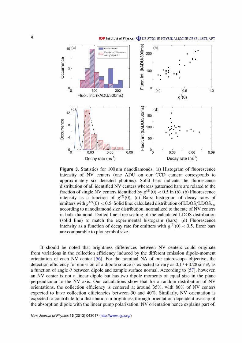
As a first step in the characterization process, we have measured the brightness of nanodiamondsthat show a clear ZPL line. Figure 3(a) shows a histogram of measured brightnesses as quantifiedby intensity on the CCD at fixed illumination intensity (solid bars). The intensity on the CCDis obtained by summing all pixels within the diffraction-limited image of each nanodiamond(green line in figure 2(a)). We observe a wide distribution of intensities, spanning from 50 × 103
to 210 × 103 ADUs on the CCD per 300 ms exposure time. At an estimated photon-to-ADUconversion factor of 6 for our CCD camera, these brightnesses correspond to 1 × 10⁶–4.2 × 10⁶
collected photons per second, at a pump power around 1 mW supplied by the CW laser. Firstly,these numbers show, at least assuming that NV centers are reasonably efficient emitters, that theabsorption cross sections of nanodiamond NV centers at a 532 nm pump wavelength are an orderof magnitude below those of dyes and II–VI quantum dot nanocrystals. Secondly, there is a widedistribution of brightnesses of over a factor 3–4 from nominally identical emitters. As describedin section 2.3, some nanodiamonds may have multiple NV centers, especially in the case of bignanoparticles. To exclude that brightness variations are due to multiple NV centers, we screenthe nanodiamonds on the basis of g(2) minimum values. Figure 3(b) shows a correlation plot,plotting the fluorescence intensities of all identified NV centers on the 100 nm nanodiamondsample versus the recorded value of g(2) at zero delay (g(2)(τ = 0)). We find that not just thebrightness, but also the minimum in g(2) is distributed with minima in g(2) ranging from 0 to0.75. The minimum in g(2) is only weakly correlated with collected intensity, especially via anapparent stepwise increase in the fluorescence intensity as g(2)(0) reaches above ≈ 0.5. Sucha stepwise increase would be expected since the minimum in g(2) scales with the number ofemitters n as 1 − 1/n. For g(2)(0)& 0.5 more than a single fluorescent center is involved in theemission, resulting in higher fluorescence intensities on average.
In the remainder we concentrate our analyses on single NV centers, i.e. those nanocrystalsfor which g(2)(0) < 0.5. In figure 3(a), we overplot a histogram of fluorescence intensities of thesubset of centers with g(2)(0) < 0.5 as patterned bars. The histogram shows a wide fluorescencedistribution, with a factor of three difference between brightest and dimmest NV centers, andwith a relative distribution of about 30% around the most frequent value. Figure 3(b) shows thatfor the single NV centers the wide distribution in fluorescence intensities notably does not showany correlation to g(2)(0) values.
New Journal of Physics 15 (2013) 043017 (http://www.njp.org/)
9
(b)
(c) (d)
0.0 0.5 1.00
100
200
Flu
or. i
nt. (
kAD
U/3
00m
s)
g2(0)
0 0.03 0.06 0.090
50
100
150
Flu
or. i
nt (
kAD
U/3
00m
s)
Decay rate (ns-1)
0 0.03 0.06 0.090
4
8
12
Occ
urre
nce
Decay rate (ns-1)
(a)
0 100 2000
5
10 All NV centers
Occ
urre
nce
Fluor. int. (kADU/300ms)
Fraction of NV centerswith g(2)(0)<0.5
Figure 3. Statistics for 100 nm nanodiamonds. (a) Histogram of fluorescenceintensity of NV centers (one ADU on our CCD camera corresponds toapproximately six detected photons). Solid bars indicate the fluorescencedistribution of all identified NV centers whereas patterned bars are related to thefraction of single NV centers identified by g(2)(0) < 0.5 in (b). (b) Fluorescenceintensity as a function of g(2)(0). (c) Bars: histogram of decay rates ofemitters with g(2)(0) < 0.5. Solid line: calculated distribution of LDOS/LDOSvac
according to nanodiamond size distribution, normalized to the rate of NV centersin bulk diamond. Dotted line: free scaling of the calculated LDOS distribution(solid line) to match the experimental histogram (bars). (d) Fluorescenceintensity as a function of decay rate for emitters with g(2)(0) < 0.5. Error barsare comparable to plot symbol size.
It should be noted that brightness differences between NV centers could originatefrom variations in the collection efficiency induced by the different emission dipole-momentorientation of each NV center [56]. For the nominal NA of our microscope objective, thedetection efficiency for emission of a dipole source is expected to vary as 0.17 + 0.28 sin2 θ , asa function of angle θ between dipole and sample surface normal. According to [57], however,an NV center is not a linear dipole but has two dipole moments of equal size in the planeperpendicular to the NV axis. Our calculations show that for a random distribution of NVorientations, the collection efficiency is centered at around 35%, with 80% of NV centersexpected to have collection efficiencies between 30 and 40%. Similarly, NV orientation isexpected to contribute to a distribution in brightness through orientation-dependent overlap ofthe absorption dipole with the linear pump polarization. NV orientation hence explains part of,
New Journal of Physics 15 (2013) 043017 (http://www.njp.org/)

10
if not the full detected intensity distribution of the NV centers in figure 3(a). Further potentialcauses of brightness variations are variations in the quantum efficiency or the absorptioncross-section as well as the dynamics of the metastable state in NV centers [58, 59] that cansignificantly affect the brightness of an NV center.
3.2. Correlation of emission rates and brightness
To examine whether quantum efficiency (QE) effects may be at play, we have measuredfluorescence decay rates for each identified single NV center. We plot a histogram of themeasured decay rates in figure 3(c). We observe a very wide distribution, with the slowestemitters decaying almost four times more slowly than the fastest ones. The most frequentlyoccurring decay rate is around γtot = 0.03 ns−1 (corresponding to about 33 ns). The time constantof 33 ns is appreciably slower than the fluorescence lifetime of NV centers in bulk diamond,for which the accepted literature value is 11.6 ns [23]. This much slower decay as well as theoccurrence of a distribution of rates is in agreement with previously reported values [49, 51].If the hypothesis that quantum efficiency variations are responsible for the large variability inbrightness in figure 3(a) is valid, one might expect a correlation between the brightness anddecay rate of the emitters. We plot the measured brightness as a function of decay rate for eachNV center in figure 3(d), which, however, displays no clear correlation. Importantly, we notethat the measured quantity here is the total decay rate γtot = γrad + γnonrad, which reflects bothvariations of radiative decay rate γrad and nonradiative decay rate γnonrad, whereas the quantumefficiency is given by γrad/γtot. Based on the collection efficiency of our microscope objective(∼10%), the count rates in figure 3 correspond to an intermediate (most data) to strong (datapoint at and above 150 kADU per 300 ms) excitation regime, where the photon emission rate isapproximately 0.2–0.9 times the total decay rate γtot. Both if one assumes to be in saturation,and below saturation, one expects the fastest decay to imply highest brightness if one assumesγnonrad to be approximately constant but γrad to be distributed. This conclusion is not stronglysupported by the data. If conversely we assume γrad to be approximately constant across NVcenters while γnonrad is distributed, one would expect the highest brightness to correlate withthe slowest decay rate (lowest γnonrad), a hypothesis also not strongly supported by the data.Specifically, we find that the subset of crystals around the most frequent brightness shows thefull spread of decay constants, while conversely also the subset of crystals that have decayconstants around the most frequent rate contains the full range of brightnesses. The lack ofstrong correlation between decay rate and brightness potentially suggests that the quantumefficiency of NV centers in nanodiamonds as we study here is distributed and not equal to unityfor all NV centers. However, as discussed in the previous section, we note that due to variationsin the collection efficiency and the unknown dipole orientation of NV centers, the interpretationof brightness in terms of quantum efficiency is convoluted. Therefore, it is essential to use awell-calibrated method in order to determine the quantum efficiency of the NV centers, as wediscuss in section 5.2.
3.3. Common local density of optical states (LDOS) argument for rate variation innanodiamonds
Many workers had already noticed that nanodiamond decay rates are widely distributed[28, 49, 51]. The variation is commonly attributed to variations solely in the radiative rate
New Journal of Physics 15 (2013) 043017 (http://www.njp.org/)
11
γrad due to a local-density-of-photonic-states effect, assuming zero nonradiative decay (i.e. unitquantum efficiency). The hypothesis, explained in detail by Inam et al [49], is that variationsare in large part due to the fact that the LDOS experienced by an NV center is influenced by thenanoscale geometry of its environment, i.e. the fact that the source is situated inside, and closeto the surface of, a very high-index nano-object that is embedded in a low-index environment.A distribution in LDOS can arise from the size distribution of nanodiamonds and from the factthat different NV centers have different dipole-moment orientation and positions within thecrystals [49, 52]. Here we assess whether this LDOS hypothesis is quantitatively reasonable.Considering that the radiative decay rate γrad(ρ) is proportional to LDOS, we evaluate theγrad(ρ) distribution by calculating the LDOS distribution assuming spherical nanoparticles, forwhich the LDOS is analytically known [60, 61]. We modeled nanodiamond NV centers as pointdipoles with randomly oriented dipole moments homogeneously distributed in position in a setof dielectric spheres with dielectric constant equal to the bulk diamond value (εsphere = 5.85).We furthermore take into account the distribution of particle size as specified according to thenanodiamond size-distribution histogram provided by the manufacturer. We make a histogramof the occurrence of LDOS values to find its probability distribution over all sphere sizes, dipolepositions and dipole configurations. The resulting LDOS distribution can be converted intoa distribution directly comparable to the experimentally measured decay rates by scaling theLDOS to the previously reported decay rate of (11.6 ns)−1
≈ 0.086 ns−1 of NV centers in bulkdiamond [23]. We note that this entire procedure involves no adjustable parameter or any fit todata. The final result is plotted in figure 3(c) as the blue solid line. The calculated histogramcorrectly predicts that emission is significantly decelerated compared to decay in bulk diamond,consistent with the fact that decay in small dielectric spheres is decelerated compared to bothvacuum and bulk dielectric. However, we observe that the calculated histogram peak falls atmuch lower decay rate than the experimentally measured histogram peak, with a discrepancyamounting to a factor of 3. A similar discrepancy between the calculated and experimentallymeasured decay rates of nanodiamond NV centers was recently reported for samples with amuch wider size distribution, centered at much larger median size, measured by Inam et al [49].We note that this discrepancy cannot be attributed to the fact that we have taken particle shapeto be simply spherical, and that we have neglected the presence of a substrate. These effectscause only small changes in the expected decay rate histogram, as verified in FDTD simulationsby Inam et al [49]. One might further argue that the occurrence of a degenerate in-plane dipolemoment [57] could skew the histogram of expected decay rates toward higher values, if oneassumes the dipole moment is free to diffuse prior to de-excitation. However, if we just makea histogram of the fastest rate instead of the average rate at each possible NV center position,the resulting histogram also does not lead to a consistent explanation (not shown). We concludethat LDOS variations in nanodiamond under the hypothesis of unit quantum efficiency and abulk decay rate of (11.6 ns)−1 do not explain the variation in measured decay rates.
3.4. LDOS argument beyond unit quantum efficiency
Inam et al proposed that although calculated and experimental absolute decay values areinconsistent on the basis of LDOS theory and the bulk rate in diamond, the calculated andexperimental results can be scaled onto each other. Indeed, if we scale the reference ratethat sets the rate axis for the calculated histogram peak not by 11.6 ns (rate constant in bulkdiamond [23]), but by a factor of 3 shorter, the calculated and measured histograms coincide
New Journal of Physics 15 (2013) 043017 (http://www.njp.org/)
12
reasonably (figure 3(c) black dotted line). Such a scaling would imply as hypothesis a unitquantum efficiency, together with an as yet hidden explanation that introduces a multiplicativecorrection factor in the calculated rate distribution.
A second hypothesis could be that no adjustment should be made of the bulk rate thatenters the comparison, but that the quantum efficiency of NV centers, while unity in bulk, isnot unity in nanocrystals. Indeed, an additive offset to the calculated histogram is introduced bynonradiative decay channels that do not occur for bulk diamond, but could occur for nanocrystalsdue to defects and the presence of large surface areas that could contain quenching sites. So far,significant nonradiative decay was evidenced only for very small nanocrystals (5 nm [54]). Adistribution of nonradiative rates around γnonrad = 0.15 ns−1 would shift the calculated histogramto the measured rates. The magnitude of the required γnonrad implies that quantum efficienciesshould be around 30–50% for the slowest nanocrystals in the measured ensemble (assumingunit efficiency in bulk).
A third hypothesis could be that the assumption that the bulk rate is entirely radiative to startwith, is incorrect, i.e. that the quantum efficiency of NV centers in bulk is significantly belowunity contrary to common assumption. Assuming a bulk quantum efficiency of 70% insteadof 100% would overlap the calculated histogram peak with the measured most frequent rate.However, this explanation would severely underestimate the width of the decay rate distributionunless a distribution of γnonrad is at play.
We conclude that LDOS variations in nanodiamond alone do not explain the variationin measured decay rates, and that a distribution of radiative and nonradiative decay constantsmust be at play for NV centers in nanodiamond. Furthermore, we conclude that an actualexperimental calibration of quantum efficiency of individual NV centers is highly desired, whichwe will return to in sections 5.1 and 5.2.
4. Statistics on small nanodiamonds
4.1. Brightness and g(2)(0)
For experiments in which nanodiamonds are intended as probes of, or sources to be embeddedin, nanophotonic environments, a size smaller than that of the 100 nm nanodiamonds wouldbe advantageous, as smaller size implies higher spatial resolution and a lower perturbativeeffect on the modes of the nanophotonic system [62, 63]. Therefore, we repeated the brightnessand decay rate statistical measurements for the 25 nm sample, i.e. the batch of crystals withmedian diameter 26 nm. For 25 nm nanodiamonds, background-subtracted g(2) measurementsshow a zero dip for all identified NV centers (for a typical 25 nm nanodiamond g(2), see e.g.figure 2(c)). The fact that we found no nanodiamonds with multiple NV centers for this sampleis commensurate with the smaller average crystal size. For these single NV centers, figure 4(a)shows a histogram of the fluorescence intensities measured on the CCD using CW illuminationat 1 mW µm−2. As in the case of the 100 nm sample, the histogram exhibits a wide fluorescenceintensity distribution, in this case spanning a factor of about two. The most frequent brightnessis approximately a factor of 2 below that of the 100 nm sample.
4.2. Distribution of rates
As in the case of the 100 nm nanocrystals, we have also measured the decay rate for all25 nm nanocrystals that we identified. The decay rate distribution, plotted as a histogram in
New Journal of Physics 15 (2013) 043017 (http://www.njp.org/)

13
0 50 1000
3
6
Occ
urre
nce
Fluor. int. (kADU/300ms)0 0.05 0.10 0.15
0
50
100
Flu
or. i
nt. (
kAD
U/3
00m
s)
Decay rate (ns-1)
0 0.05 0.10 0.150
5
10
15
Occ
urre
nce
Decay rate (ns-1)
0.147 0.154 0.161
0
7
14
LDOS/LDOSVAC
Poc
curr
ence
(%
)
(a) (b)
(c)
Figure 4. Statistics for 25 nm nanodiamonds. (a) Histogram of fluorescenceintensity (one ADU on our CCD camera corresponds to approximately sixdetected photons). (b) Fluorescence intensity as a function of decay rate. (c) Bars:histogram of the measured decay rates of NV centers. Solid blue line: calculateddistribution of LDOS/LDOSvac (shown in the inset) according to nanodiamondsize distribution, normalized to the rate of NV centers in bulk diamond. Solidblack line: free scaling of the calculated LDOS distribution (blue line) so as tomatch the experimental histogram (bars).
figure 4(c), again shows a very wide distribution, with a factor of 4 contrast in decay rate. Wefind higher decay rates on average compared to 100 nm nanodiamonds, with a most frequentdecay rate around γtot = 0.035 ns−1 (corresponding to about 28 ns). The most frequent decayrate is approximately 25% faster than for the 100 nm nanodiamonds. Exactly as in the case of100 nm nanodiamonds, the wide distribution of fluorescence brightness and decay rates does notimply a correlation between the two. As confirmation, in figure 4(b) we plot the fluorescenceintensities and decay rates of 25 nm diamond NV centers, where we find no clear correlation.
4.3. Comparison with the LDOS argument for distribution of rates
To assess whether the common hypothesis that the distribution in rate is due to a distributionin LDOS is valid for small nanodiamonds, we calculated the LDOS distribution (plotted inthe inset of figure 4(c)) also for the 25 nm sample taking into account the size distributionhistogram measured by the nanodiamond supplier. The rate distribution expected from thecalculated LDOS scaled with the bulk rate (blue solid line in figure 4(c)) is firstly considerably
New Journal of Physics 15 (2013) 043017 (http://www.njp.org/)
14
narrower than the experimental decay rate distribution, and secondly at considerably reducedrate compared to the measured decay rates. The magnitude of the discrepancy in decay rate isapproximately a factor of 6, i.e. twice larger than for the 100 nm nanodiamonds. A scaling of thecalculated distribution by a multiplicative factor (here a factor of about 6) as proposed by Inamet al [49] does not lead to a good correspondence as in the 100 nm case, as the relative widthof the measured histogram far exceeds that of the scaled calculation (black line in figure 4(c)).Taking our data on both 100 and 25 nm nanodiamonds together, we hence do not find supportfor the hypothesis by Inam et al that a hitherto hidden effect multiplies the radiative rate ofNV centers in nanocrystals compared to bulk diamond. A more likely explanation that does notinvolve a scaling of γrad due to an unknown origin is that NV centers are subject to a distributionof nonradiative rates on top of the LDOS-induced radiative rate distribution. The measureddistribution of 25 nm nanodiamond decay rates points to a wide distribution of nonradiativerates. According to this hypothesis, those crystals with decay around the most-frequent decayrate of 0.035 ns−1 must have a quantum efficiency below 15–20%, twice as low as for the100 nm nanocrystals. The overall lower quantum efficiency estimate is commensurate with thereduction in average brightness, and is also consistent with the fact that a larger sensitivity tononradiative decay channels is potentially associated with the increased nanocrystal surface-to-volume ratio.
5. LDOS tuning on single nitrogen–vacancy (NV) centers
Our data indicate that NV centers even in nanocrystals as large as 100 nm across do not have unitquantum efficiency, and that there is a distribution of nonradiative and radiative rates. Therefore,it is desirable to measure quantum efficiency, γrad and γnonrad independently on individual NVcenters in order to decide if/which NV centers in nanodiamonds are suitable for use as LDOSprobes for integration in nanophotonic devices. In the literature, several reports have appearedthat evidence lifetime changes of NV emission that are induced by placing nanocrystals inphotonic environments of varying index and topology [36, 38, 39, 49, 51]. To our knowledgeall these measurements of lifetime changes for nanodiamonds were performed by comparingthe mean rate from an ensemble of single-center measurements in one system, to measurementon a different ensemble of single centers in a second system [38, 49, 51]. Ruijgrok et al [51]in particular report changes for a system in which the induced LDOS change is exactly known,and report changes in the mean rate consistent with those expected for unit-quantum-efficiencyemitters. However, we note that in these ensemble measurements, the change of the mean decayrate was far smaller than the width of the rate distribution. Therefore, those measurements donot allow us to ascertain whether for any given single NV center the rate actually varies withvarying LDOS in a manner that is consistent with the expectations for efficient emitters.
We perform measurements in which we change the LDOS of single NV centers in twoways. Firstly, we have immobilized the nanocrystals by evaporating a thin layer of SiO2,and then introduced liquids with different refractive indices to systematically modify theLDOS around the NV centers (section 5.1). Secondly, we have used nanomechanical tuningof LDOS using a piezo-controlled mirror to effect a Drexhage experiment [68–72] on singlenanodiamonds (section 5.2). The nanomechanical method is preferable since it rapidly allowscontinuous variation of LDOS. Due to their smaller apparent brightness, however, we wereunable to apply the technique also to 25 nm diamond nanocrystals as the much higher pumpenergy required to reach appreciable count rates caused thermal breakdown of the micro-mirror.
New Journal of Physics 15 (2013) 043017 (http://www.njp.org/)
15
Therefore, we applied the liquid-tuning method (section 5.1) to the small nanodiamonds, andreport on the nanomechanical method for the large nanodiamonds (section 5.2).
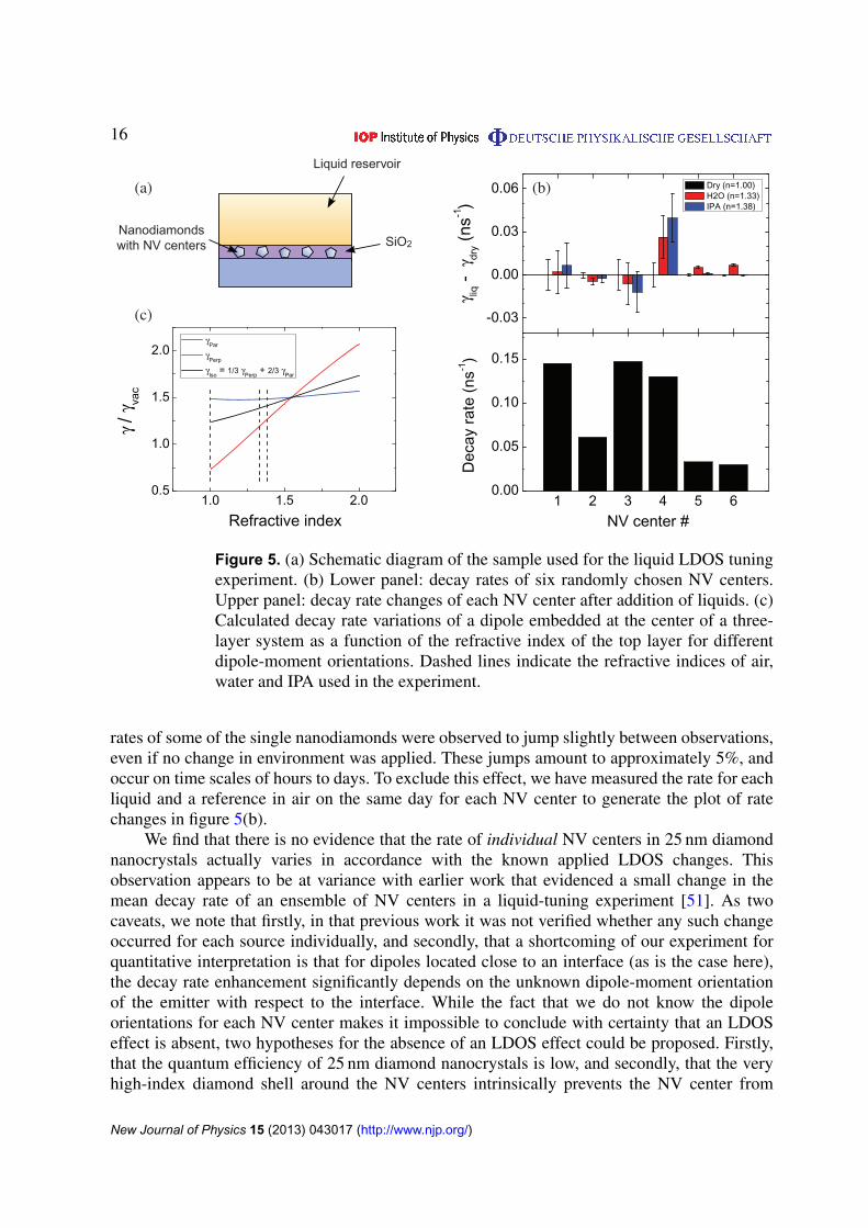
5.1. Liquid tuning of LDOS on single NV centers in small nanodiamonds
For the small nanodiamonds, only the liquid-tuning method could be applied due toexperimental constraints. The idea and first implementation of this method was pioneered bySnoeks et al [64], and later adopted by e.g. [51, 65, 67]. Emitters are placed in close proximityto a planar interface between a dielectric and a half-space that can be filled with liquids ofdifferent refractive index. The advantage of using liquid tuning of refractive index for sourcesnear an interface is that the LDOS changes near an interface are nearly independent of emissionfrequency, and are known to be excellently described by the theory explained in full by Urbachand Rikken [66]. In view of the broad emission spectrum of NV centers in diamond, it isimportant to apply a broadband LDOS change when seeking to measure lifetime changes. Anarrowband LDOS variation as obtained with a high-Q microcavity that would for instancebe tuned to the ZPL would not necessarily affect the rate, but rather only the branching ratiobetween the ZPL and the rest of the spectrum.
We prepared the sample by evaporating a 60 nm thick layer of SiO2 on one of the 25 nmnanodiamond samples on which we had identified single NV centers. This step immobilizes thenanodiamonds, and ensures that liquid application to tune LDOS does not add new chemicallyinduced nonradiative decay channels. Next, we defined a 3 mm deep liquid reservoir on top ofthe sample using a ring-shaped enclosure cut from polydimethylsiloxane (PDMS) bonded tothe substrate. Figure 5(a) depicts a schematic of the sample. In order to investigate the decaydynamics of the NV centers in response to the LDOS variations, we randomly selected six NVcenters from the ensemble of figure 4 and measured their lifetimes under three conditions: beforeadding any liquids where the top half-space of nanodiamonds consists of air (n = 1.00), afteradding water with a refractive index of n = 1.33, and after adding isopropyl alcohol (IPA) with arefractive index of n = 1.38 to the liquid bath on top of the nanodiamonds. In the lower panel offigure 5(b), we plot the decay rate of each NV center as a black bar measured when the sample isdry. The color bars in the upper panel of figure 5(b) show the difference between decay rates ofeach NV center after and before introducing a liquid. We observe that for most centers, the decayrate either barely varies, or varies nonmonotonically with applied index, although generally oneexpects to observe an increase in the decay rate of a dipole emitter in a homogeneous mediumby increasing the refractive index of the environment due to an increase of the LDOS [66].
For comparison with the data, we calculate the normalized decay rate of a dipole positionedin the middle of a 60 nm thick SiO2 slab (n = 1.52) which is sandwiched between a semi-infiniteslab of quartz with n = 1.46 at the bottom and a semi-infinite slab with varying refractive indexat the top. Figure 5(c) shows the calculated decay rate of the dipole as a function of the refractiveindex of the top layer for different dipole-moment orientations. The calculation shows that asthe refractive index increases the decay rate change is expected to be monotonic and increasingand is the largest for a dipole oriented perpendicular to the interface while the change is slightfor a dipole-moment parallel to the interface. Comparing the calculated rate changes with themeasured decay rates (figure 5(b)), we find no systematic rate variation for the NV centerswithin the error bars of our experimental data. The error bar for measurements on individual NVcenters is composed of two contributions. Firstly, the error bar contains the uncertainty in the fitto the fluorescence decay trace. Secondly, the experiment is hampered by the fact that the decay
New Journal of Physics 15 (2013) 043017 (http://www.njp.org/)
16
(b)
Nanodiamondswith NV centers SiO2
Liquid reservoir
(a)
(c)
1.0 1.5 2.00.5
1.0
1.5
2.0
γ / γ
vac
Refractive index
γPar
γPerp
γIso
= 1/3 γPerp
+ 2/3 γPar
-0.03
0.00
0.03
0.06
γ liq -
γdr
y (ns
-1)
Dry (n=1.00) H2O (n=1.33) IPA (n=1.38)
1 2 3 4 5 60.00
0.05
0.10
0.15
Dec
ay r
ate
(ns-1
)
NV center #
Figure 5. (a) Schematic diagram of the sample used for the liquid LDOS tuningexperiment. (b) Lower panel: decay rates of six randomly chosen NV centers.Upper panel: decay rate changes of each NV center after addition of liquids. (c)Calculated decay rate variations of a dipole embedded at the center of a three-layer system as a function of the refractive index of the top layer for differentdipole-moment orientations. Dashed lines indicate the refractive indices of air,water and IPA used in the experiment.
rates of some of the single nanodiamonds were observed to jump slightly between observations,even if no change in environment was applied. These jumps amount to approximately 5%, andoccur on time scales of hours to days. To exclude this effect, we have measured the rate for eachliquid and a reference in air on the same day for each NV center to generate the plot of ratechanges in figure 5(b).
We find that there is no evidence that the rate of individual NV centers in 25 nm diamondnanocrystals actually varies in accordance with the known applied LDOS changes. Thisobservation appears to be at variance with earlier work that evidenced a small change in themean decay rate of an ensemble of NV centers in a liquid-tuning experiment [51]. As twocaveats, we note that firstly, in that previous work it was not verified whether any such changeoccurred for each source individually, and secondly, that a shortcoming of our experiment forquantitative interpretation is that for dipoles located close to an interface (as is the case here),the decay rate enhancement significantly depends on the unknown dipole-moment orientationof the emitter with respect to the interface. While the fact that we do not know the dipoleorientations for each NV center makes it impossible to conclude with certainty that an LDOSeffect is absent, two hypotheses for the absence of an LDOS effect could be proposed. Firstly,that the quantum efficiency of 25 nm diamond nanocrystals is low, and secondly, that the veryhigh-index diamond shell around the NV centers intrinsically prevents the NV center from
New Journal of Physics 15 (2013) 043017 (http://www.njp.org/)
17
responding to (moderate) changes in the LDOS of the environment it is supposed to probe. Weexclude the latter explanation on the basis of a set of finite element (COMSOL) simulations, inwhich we calculate the decay rate of a point dipole randomly located in a diamond nanosphere,which in turn is placed at varying distances from a planar interface with materials of variousdielectric constants. We find that in all cases, the decay rate of the source simply follows thetheory of Urbach and Rikken [66] for a source without a dielectric shell, multiplied by a pre-factor that is essentially a quasistatic local-field correction factor due to the diamond shell andis independent of the varying LDOS.
To conclude, our observation that no NV center responds to LDOS changes together withour earlier correlation plots of brightness versus decay rate (figures 3 and 4) means that thequantum efficiencies of 25 nm diamond nanocrystals are low. A second important conclusionis that single NV centers of 25 nm size appear unsuitable to measure LDOS changes dueto the slight jumps in lifetime, unless the entire measurement scheme (including referencemeasurements) takes less than a few hours.
5.2. Nanomechanical tuning of LDOS on large nanodiamonds
In this section we report on the results of a second method to assess whether single NVcenters are suited for LDOS measurements, and to calibrate emission rates. This second methodhas the advantage that we can apply calibrated LDOS changes rapidly so that jumps in theintrinsic rate constants can be avoided that hamper experiments where macroscopic samplechanges are required to modify LDOS, as in a liquid immersion experiment. The scheme issimilar to a measurement procedure reported by Buchler et al [73], based on a Drexhageexperiment [68–72]. In a Drexhage experiment, a mirror is used to impose a large LDOSchange, and rates are measured as a function of the emitter–mirror separation. While this methodis usually implemented by creating a set of macroscopic samples where mirrors are coatedwith spacers of calibrated thicknesses [69–71] or by creating a single sloping wedge betweena mirror and an ensemble of emitters [72], Buchler et al realized a nanomechanical versionthat can be applied to a single emitter. Buchler et al used a silver-coated curved fiber end asa mirror attached to a piezostage to precisely tune the mirror distance to an underlying singleemitter on the sample [73]. Here, we use a similar method in a shear-force-feedback near-fieldmicroscope. However, instead of a vertical mirror displacement, we use a lateral displacement ofthe curved mirror while staying in shear-force feedback to keep the mirror and sample substratein near-contact. As the contact point moves sideways, the spherical mirror shape ensures that themirror-to-emitter distance varies (figure 6(a)). To fabricate the curved mirror, we glued 45 µmpolystyrene beads (Polysciences, Inc.) to the end of cleaved optical fibers and coated the beadswith about 200 nm of silver.
We have applied the scanning-mirror LDOS-changing technique to 100 nm nanodiamondscontaining single NV centers, prepared as described in section 2.1, and subsequently embeddedin a 200 nm thick layer of planarizing spin-on glass (FOX-14, Dow Corning). The spin-on glassimmobilizes the nanocrystals, so that they are not moved during shear-force scanning. In orderto vary the distance between the mirror and the emitter, we scan the mirror bead laterally ontop of an identified NV center. For each position of the mirror bead, we collect the fluorescenceemission of the NV center, positioned at the focus of the pump laser, through the confocalmicroscope setup described in section 2.2. By scanning the mirror bead, we obtain a confocalfluorescence intensity map as shown in figure 6(b). Here, each pixel represents the relative
New Journal of Physics 15 (2013) 043017 (http://www.njp.org/)

18
Figure 6. (a) Schematic diagram of the nanomechanical tuning of LDOS for100 nm nanodiamonds. (b) Fluorescence intensity map of an NV center (NVcenter 1 in table 1) as a function of mirror lateral displacement. (c) Correspond-ing decay rate map of the NV center as a function of mirror lateral displacement.Decay rates are extracted from a single-exponential fit to the time-trace datafor each pixel. (d) Dots: decay rate as a function of the emitter distance to themirror, extracted from the decay rate map shown in (c). Solid line: fitted LDOSon the measured rate oscillations with fit parameters γrad, γnonrad and a set ofdipole-moment orientations. The shown quantum efficiency (QE) is the most-likely value. (e) and (f) Decay rate as a function of emitter–mirror distance fortwo other NV centers (numbers 4 and 5 in table 1, respectively) and the fittedrate from LDOS calculation.
New Journal of Physics 15 (2013) 043017 (http://www.njp.org/)

19
position of the mirror bead with respect to the NV center with the false color representingthe collected fluorescence intensity. We clearly observe interference rings in the fluorescenceintensity map. These rings mainly stem from the fact that the mirror imposes a standing-wave pattern on the 532 nm pump field, which subsequently results in a modulation of thefluorescence intensity.
For each pixel in the fluorescence intensity map, we stored absolute photon arrival times,as well as laser pulse arrival times, allowing us to extract the decay dynamics. We use a single-exponential fit to obtain the corresponding decay rate of the emitter for each mirror position, asplotted in figure 6(c). Here, the color scale represents the fitted decay rate corresponding to adefined mirror position. Interestingly, we observe a radial modulation of the decay rates varyingbetween about 0.02 and 0.04 ns−1, which we attribute to the varying LDOS in front of the mirror.To quantify the variation as a function of the distance from the emitter to the mirror, we extractedthe decay rates as a function of the lateral distance to the mirror central position. To this end,we bin pixels in concentric rings of equal lateral distance to the mirror center, and concatenatethe photon-correlation time traces of all pixels in each bin to obtain a single fluorescence decaytrace per radial distance. Using the spherical form factor of the bead, we convert lateral positionof the mirror to normal distance of the mirror to emitter. The decay rate fitted to the fluorescencedecay for each mirror–emitter separation is depicted in figure 6(d) (black dots). We observe adistinct oscillation of the rate around 0.028 ns−1, with a 15% amplitude. To our knowledge, thisis the first report of a reversible change in the decay rate of a single NV center in a calibratedLDOS experiment.
Due to the large radius of the mirror compared to its distance to emitters, it is reasonableto consider the experimental configuration as a planar glass–air–mirror system in whichwe vary the air thickness. For this system, the LDOS is exactly known [17, 71] for anydipole orientation and position. We fit the experimental decay rate data using the theoreticalLDOS ρ(z, d, θ) according to γ (z) = γnonrad + γrρ(z, d, θ), where the fit parameters are thenonradiative decay rate γnonrad, the radiative decay rate γrad and the dipole orientation θ relativeto the normal to the plane. Finally a small offset d appears that is due to the unknown distance-of-closest approach in shear-force microscopy, of the order of 15 nm. Care must be takenthat a correlation exists between the dipole orientation θ and the apparent quantum efficiencyγrad/(γnonrad + γrad) returned by the fit routine, due to the fact that the LDOS for different dipole-moment orientations is similar in qualitative z-dependence, but different in oscillation contrast.To overcome this dependence, we examine fits of the rate oscillations for a set of dipoleorientations and evaluate the goodness of fit individually. The goodness of fit is establishedby measuring how far the residuals of the fit (point-by-point deviation between data and fitfunction) are within the data-point error bar. This gives a range of quantum efficiency values forwhich the fit is consistent with the data. In this paper we report the range of quantum efficiencyvalues consistent with the data given that the dipole orientation should be treated as an unknownparameter. In the case that the dipole-moment orientation of the NV center is known, whichcould in principle be realized using Fourier microscopy [74], one can extract a more precisevalue for the quantum efficiency. For the particular data set shown in figure 6(d), we find a mostlikely quantum efficiency of 26% and a dipole-moment orientation within 20◦ along the sampleplane. The range of quantum efficiencies consistent with the data for this NV center is boundedfrom below by 26%, and from above by 50%. To our knowledge this is the first experimentalcalibration of the quantum efficiency of a single NV center in a diamond nanocrystal.
New Journal of Physics 15 (2013) 043017 (http://www.njp.org/)

20
Table 1. Extracted quantum efficiencies, rates and brightnesses for five randomlychosen NV centers in 100 nm nanodiamonds. Quantum efficiencies are quotedas a range of values, taking into account that the dipole orientation is a freeparameter. In this fit procedure, the proper fit parameters are the quantumefficiency and the total decay rate, which has a small error bar. For completenesswe also show the two derived quantities γrad and γnonrad. These rates and theirerror bars are given as fitted when fixing the dipole orientation to its mostlikely value. Fitted brightnesses were converted to CCD response units tobe comparable with figure 3 (one ADU on our CCD camera corresponds toapproximately six detected photons).
NV center no. 1 2 3 4 5
QE range (%) 26–50 23–45 27–58 9–14 58–90γtot (ns−1
× 10−3) 25.7 ± 0.2 29.2 ± 0.2 33.9 ± 0.4 42.2 ± 0.2 39.7 ± 0.9γrad (ns−1
× 10−3) 6.7 ± 0.5 6.8 ± 0.6 9 ± 1 4.0 ± 0.4 23 ± 3γnonrad (ns−1
× 10−3) 19.0 ± 0.5 22.5 ± 0.6 25 ± 1 38.2 ± 0.5 17 ± 3Brightness (kADU per 300 ms) 102 112 139 144 135
In order to investigate the typical quantum efficiencies of NV centers, we selected fiverandom NV centers and examined them with the moving mirror experiment as explained above.Each nanodiamond was selected to be a single NV center containing a nanocrystal accordingto the criteria we outlined in section 2.3, without further post-selection for inclusion in theDrexhage experiment. Table 1 summarizes the confidence intervals for the fitted values of thequantum efficiencies, given that we do not know the dipole orientation a priori. The totaldecay rate γtot, i.e. the sum of γrad and γnonrad, varies almost over a factor of 2, and can befitted accurately. In table 1 we also report radiative and nonradiative decay rates. Values arereported as fitted to the data while fixing the dipole orientation at its most likely value, inwhich case the data can be fitted with small error bars on γrad and γnonrad. The wide range ofquantum efficiencies consistent with the data of course imply that in a completely free fit γrad
and γnonrad both have a large error bar, though their sum γtot does not. We find that the differentNV centers we probed, while having reasonably comparable brightness, in fact have widelydifferent quantum efficiencies. For instance, NV center 4 (figure 6(e)) has an efficiency certainlybelow 14%, whereas NV center 5 (figure 6(f)) has a quantum efficiency certainly above 58%, inthe range 58–90%. Furthermore, we note that the fits neither result in the conclusion of a fixednonradiative rate at varying radiative rate, nor conversely in the conclusion that the radiative rateis a constant while the nonradiative rate varies. Instead, both the radiative and the nonradiativedecay rates are distributed. Even with the wide error bars on quantum efficiencies, we establishthat both distributions span at least around a factor of 2 in range. Our measurements henceshow that the common tacit assumption of near-unity quantum efficiency and nearly identicalemission characteristics barring those due to depolarization factors in the nanodiamonds shouldbe discarded.
6. Conclusion
In order to assess the suitability of nanodiamonds as photonic LDOS probes and as buildingblocks for hybrid photonic systems, we have investigated the brightness, decay rate and quantum
New Journal of Physics 15 (2013) 043017 (http://www.njp.org/)
21
efficiency of single NV centers in nanodiamonds of 25 nm and of 100 nm median size. Forboth size ranges a wide distribution in brightnesses and rates is found, consistent with reportsby earlier workers. We conclude that the wide distribution of rates is due to a distribution inradiative rates, nonradiative rates and quantum efficiencies. This conclusion contradicts earlierwork, that interpreted the wide distribution of decay rates as mainly due to a photonic effectthat causes a distribution in radiative decay rates via the LDOS. Instead, our measurementsshow that even NV centers in large nanocrystals show a wide range of quantum efficiencieswhen probed in a controlled LDOS experiment. For NV centers in 100 nm nanocrystals we findquantum efficiencies distributed between 10 and 90%, while for the smaller NV centers thequantum efficiency for fluorescence is likely a factor of 2 smaller on average.
For applications in nanophotonic experiments using single NV centers, a highlyproblematic property is that quantum efficiency does not correlate with brightness, due to thefact that both the radiative and nonradiative rates are distributed. In other words, screeningnanodiamonds to pick the best one to probe LDOS or for incorporation in a photonic devicecannot rely on a simple metric such as spectrum or brightness. Instead, we argue that futurework in the hybrid assembly of nanodiamonds in plasmonics and photonic crystals to realizeaccelerated spontaneous emission decay always requires an experimental protocol in whichnanodiamonds are first individually calibrated in terms of quantum efficiency. While we haveshown a method for such calibration, this is a highly tedious procedure that is not easilyimplementable and requires dedicated near-field manipulation equipment.
In this work, we have not speculated on the origin of the apparent low quantum efficiencyof single NV centers in nanodiamonds. We close with two remarks on the origin of the lowapparent quantum efficiency. Firstly, we have treated the NV center as a quasi-two-level system.Our experiments thus address the question of what the apparent quantum efficiency is whenattempting to use an NV center as a two-level LDOS probe. From the NV center spectrum,it is clear that the spectrum is very wide with large vibrational broadening. Moreover, it iswell known that the NV− center is not a two-level system. Instead, the NV− has different spinsublevels, and may experience spin-flip intersystem crossing between allowed spin transitionmanifolds. The rates for these transitions were recently characterized in detail for NV centers inbulk diamond in [58]. A further complication is that the NV− defect may infrequently transitionto an uncharged NV center that also luminesces, yet at a different rate and efficiency. The manyrates involved in these transitions can further vary between NV centers due to, e.g., variations incrystal strain. A full treatment of the response of NV centers to LDOS changes would hencehave to treat the full rate equations in which radiative transition rates are, and intersystemcrossing rates are not, affected by LDOS. An important step beyond our work will be toperform the measurements we have described here but employing the spin selective techniquesreported by Robledo et al [58] to establish what the nonradiative and radiative rates are foreach transition separately, instead of lumping rates into effective two-level parameters. Whilethe LDOS changes we have applied using a mirror are broadband LDOS changes that modifyradiative transitions roughly equally across the emission spectrum, LDOS changes that havestrong spectral features could be used advantageously to enhance or suppress the importance ofintersystem crossing.
Having established that further work is required to separate the quantum efficienciesreported here into parameters per transition in a more complete level scheme, we turn to possiblereasons for the below-unity values of quantum efficiency that we find. The lower brightness ofthe smaller NV centers, as well as their lack of response to LDOS changes suggest that the
New Journal of Physics 15 (2013) 043017 (http://www.njp.org/)

22
surface, i.e. surface contamination with carbon, or surface defects may play a role in providingquenching sites. Indeed, it has already been suggested for very small (5 nm) nanodiamonds thatNV centers may suffer quenching due to graphite shells on the diamonds [54, 75]. While thenanodiamonds we used have been employed by several groups in spontaneous emission controlexperiments in untreated form, exactly as in our experiments, additional surface treatmentssuch as prolonged immersion in boiling sulfuric acid, or cleaning in Koningswasser have beenproposed by several workers. Whether or not such treatments actually affect quantum efficiencyis as yet unclear, as is whether quenching can be completely suppressed. We propose thatthe quantum efficiency calibration method that we demonstrated will be an indispensable toolto evaluate such cleaning methods, as well as to screen other color centers in diamond foradvantageous fluorescence properties.
Acknowledgments
We thank S Schietinger for communications regarding sample preparation methods, M Frimmerfor experimental help and discussions, and C Osorio for suggestions to improve the paper. Thiswork was part of the research program of the ‘Foundation for Fundamental Research on Matter(FOM)’, which was financially supported by the ‘The Netherlands Organization for ScientificResearch (NWO)’. AFK gratefully acknowledges a NWO-Vidi grant for financial support.
References
[1] Santori C, Fattal D and Yamamoto Y 2010 Single-Photon Devices and Applications (New York: Wiley)[2] Vahala K (ed) 2005 Optical Microcavities (Advanced Series in Applied Physics vol 5) (Singapore: World
Scientific)[3] Bleuse J, Claudon J, Creasey M, Malik N S, Gerard J M, Maksymov I, Hugonin J P and Lalanne P 2011
Phys. Rev. Lett. 106 103601[4] Gerard J M and Gayral B 1999 J. Light. Technol. 17 2089–95[5] Reithmaier J P, Sek G, Loffler A, Hofmann C, Kuhn S, Reitzenstein S, Keldysh L V, Kukalovskii V D,
Reinecke T L and Forchel A 2004 Nature 432 197[6] Yoshie T, Scherer A, Hendrickson J, Khitrova G, Gibbs H M, Rupper G, Ell C, Shchekin O B and Deppe D G
2004 Nature 432 200–3[7] Englund D, Fattal D, Waks E, Solomon G, Zhang B, Nakaoka T, Arakawa Y, Yamamoto Y and Vuckovic J
2005 Phys. Rev. Lett. 95 013904[8] Noda S, Fujita M and Asano T 2007 Nature Photon. 1 449[9] Yao P, Manga Rao V S C and Hughes S 2010 Laser Photon. Rev. 4 499
[10] Thyrrestrup H, Sapienza L and Lodahl P 2010 Appl. Phys. Lett. 96 231106[11] Sapienza L, Thyrrestrup H, Stobbe S, Garcia P D, Smolka S and Lodahl P 2010 Science 327 1352–5[12] Akimov A V, Mukherjee A, Yu C L, Chang D E, Zibrov A S, Hemmer P R, Park H and Lukin M D 2007
Nature 450 402–6[13] Ma R M, Oulton R F, Sorger V J, Bartal G and Zhang X 2011 Nature 10 110–3[14] Koenderink A F 2009 Nano Lett. 9 4228[15] Curto A G, Volpe G, Taminiau T H, Kreuzer M P, Quidant R and van Hulst N F 2010 Science 329 930–3[16] Sprik R, van Tiggelen B A and Lagendijk A 1996 Europhys. Lett. 35 265–70[17] Novotny L and Hecht B 2006 Principles of Nano-Optics (Cambridge: Cambridge University Press)[18] Lounis B and Orrit M 2005 Rep. Prog. Phys. 68 1129–79[19] Leatherdale C A, Woo W K, Mikulec F V and Bawendi M G 2002 J. Phys. Chem. B 106 7619–22
New Journal of Physics 15 (2013) 043017 (http://www.njp.org/)
23
[20] Donega C D, Hickey S G, Wuister S F, Vanmaekelbergh D and Meijerink A 2003 J. Phys. Chem. B 107 489[21] Brouri R, Beveratos A, Poizat J P and Grangier P 2000 Opt. Lett. 25 1294[22] Kurtsiefer C, Mayer S, Zarda P and Weinfurter H 2000 Phys. Rev. Lett. 85 290[23] Beveratos A, Brouri R, Gacoin T, Poizat J P and Grangier P 2001 Phys. Rev. A 64 061802[24] van der Sar T, Wang Z H, Blok M S, Bernien H, Taminiau T H, Toyli D M, Lidar D A, Awschalom D D,
Hanson R and Dobrovitski V V 2012 Nature 484 82[25] Robledo L, Childress L, Bernien H, Hensen B, Alkemade P F A and Hanson R 2011 Nature 477 574[26] Maze J R et al 2008 Nature 45 644[27] Horowitz V R, Aleman B J, Christle D J, Cleland A N and Awschalom D D 2012 Proc Natl. Acad. Sci. USA
109 13493[28] Tisler J et al 2009 ACS Nano 3 1959[29] Faraon A, Santori C, Huang Z H, Acosta V M and Beausoleil R G 2012 Phys. Rev. Lett. 109 033604[30] Santori C, Barclay P E, Fu K M C, Beausoleil R G, Spillane S and Fisch M 2010 Nanotechnology 21 274008[31] Babinec T M, Hausmann J M, Khan M, Zhang Y, Maze Y R, Hemmer P R and Loncar 2010 Nature
Nanotechnol. 5 195[32] Schroder T, Gadeke F, Banholzer M J and Benson O 2011 New J. Phys. 13 055017[33] Fu K M C, Barclay P E, Santori C, Faraon A and Beausoleil R G 2011 New J. Phys. 13 055023[34] Faraon A, Barclay P E, Santori C, Fu K M C and Beausoleil R G 2011 Nature Photon. 5 301[35] Benson O 2011 Nature 480 193–9[36] Schietinger S, Barth M, Aichele T and Benson O 2009 Nano Lett. 9 1694[37] van der Sar T, Hagemeier J, Pfaff W, Heeres E C, Thon S M, Kim H, Petroff P M, Oosterkamp T H,
Bouwmeester D and Hanson R 2011 Appl. Phys. Lett. 98 193103[38] Kolesov R, Grotz B, Balasubramanian G, Stohr R J, Nicolet A A L, Hemmer P R, Jelezko F and Wrachtrup
J 2009 Nature Phys. 5 470–4[39] Huck A, Kumar S, Shakoor A and Andersen U L 2011 Phys. Rev. Lett. 106 096801[40] Michaelis J, Hettich C, Mlynek J and Sandoghdar V 2000 Nature 405 325–8[41] Cuche A, Drezet A, Sonnefraud Y, Faklaris O, Treussart F, Roch J F and Huant S 2009 Opt. Express
17 19969–80[42] Cuche A, Mollet O, Drezet A and Huant S 2010 Nano Lett. 10 4566–70[43] Frimmer M, Chen Y and Koenderink A F 2011 Phys. Rev. Lett. 107 123602[44] Degen C L 2008 Appl. Phys. Lett. 92 243111[45] Taylor J M, Cappellaro P, Childress L, Jiang L, Budker D, Hemmer P R, Yacoby A, Walsworth R and Lukin
M D 2008 Nature Phys. 4 810–6[46] Balasubramanian G et al 2008 Nature 455 648–51[47] Maletinsky P, Hong S, Grinolds M S, Hausmann B, Lukin M D, Walsworth R L, Loncar M and Yacoba A
2012 Nature Nanotechnol. 7 320–4[48] Bradac C, Gaebel T, Naidoo N, Rabeau J R and Barnard A S 2009 Nano Lett. 9 3555[49] Inam F A, Gaebel T, Bradac C, Stewart L, Withford M J, Dawes J M, Rabeau J R and Steel M J 2011
New J. Phys. 13 073012[50] Tizei L H G and Kociak M 2012 Nanotechnology 23 175702[51] Ruijgrok P V, Wuest R, Rebane A A, Renn A and Sandoghdar V 2010 Opt. Exp. 18 6360[52] Schniepp H and Sandoghdar V 2002 Phys. Rev. Lett. 89 257403[53] Schietinger S 2011 private communication[54] Bradac C, Gaebel T, Naidoo N, Sellars M J, Twamley J, Brown L J, Barnard A S, Plakhotnik T, Zvyagin A V
and Rabeau J R 2010 Nature Nanotechnol. 5 345[55] Schietinger S, Schroder T and Benson O 2008 Nano Lett. 8 3911[56] Chapman R and Plakhotnik T 2011 Chem. Phys. Lett. 507 190[57] Alegre T P M, Santori C, Medeiros-Ribero G and Beausoleil R G 2007 Phys. Rev. B 76 165205[58] Robledo L, Bernien H, van der Sar T and Hanson R 2011 New J. Phys 13 025013
New Journal of Physics 15 (2013) 043017 (http://www.njp.org/)
24
[59] Plakhotnik T, Moerner W E, Palm V and Wild U P 1995 Opt. Commun. 114 83[60] Tai C T 1994 Dyadic Green Functions in Electromagnetic Theory (Piscataway, NJ: IEEE)[61] Mertens H, Koenderink A F and Polman A 2007 Phys. Rev. B 76 115123[62] Koenderink A F, Buchler B C, Kafesaki M and Sandoghdar V 2005 Phys. Rev. Lett. 95 153904[63] van der Sar T, Hagemeier J, Pfaff W, Heeres E, Thon S, Kim H, Petroff P, Tjerk O, Bouwmeester D and
Hanson R 2012 J. Opt. Soc. Am. B 29 698–703[64] Snoeks E, Lagendijk A and Polman A 1995 Phys. Rev. Lett. 74 2459–62[65] Hensen T M, de Dood M J A and Polman A 2000 J. Appl. Phys. 88 5142[66] Urbach H P and Rikken G L J A 1998 Phys. Rev. A 57 3913–30[67] Walters R J, Kalkman J, Polman A, Atwater H A and de Dood M J A 2006 Phys. Rev. B 73 132302[68] Drexhage K H 1970 J. Lumin. 1–2 693[69] Leistikow M D, Johansen J, Kettelarij A J, Lodahl P and Vos W L 2009 Phys. Rev. B 79 045301[70] Andersen M L, Stobbe S, Sørensen A S and Lodahl P 2011 Nature Phys. 7 215–8[71] Amos R M and Barnes W L 1997 Phys. Rev. B 55 7249[72] Kwadrin A and Koenderink A F 2012 J. Phys. Chem. C 116 16666[73] Buchler B C, Kalkbrenner T, Hettich C and Sandoghdar V 2005 Phys. Rev. Lett. 95 063003[74] Lieb M A, Zavislan J M and Novotny L 2004 J. Opt. Soc. Am. B 21 1210–5[75] Smith B R, Inglis D W, Sandnes B, Rabeau J R, Zvyagin A V, Gruber D, Noble C J, Vogel R, Osawa E and
Plakhotnik T 2009 Small 5 1649
New Journal of Physics 15 (2013) 043017 (http://www.njp.org/)