Sublimation of 6,13-pentacenequinone from pentacene single ... · Sublimation of...
50
1 Sublimation of 6,13-pentacenequinone from pentacene single crystal surfaces Gerard van Bemmel Master thesis Chemical Technology Enschede, May 2009 Faculty of Science and Technology Inorganic Materials Science Mesa + Institute for Nanotechnology University of Twente
Transcript of Sublimation of 6,13-pentacenequinone from pentacene single ... · Sublimation of...
1
Sublimation of 6,13-pentacenequinone from pentacene
single crystal surfaces
Gerard van Bemmel
Master thesis Chemical Technology
Enschede, May 2009
Faculty of Science and Technology
Inorganic Materials Science
Mesa+ Institute for Nanotechnology
University of Twente
2
Summary
Pentacene has become an important model system for the fundamental studies on
organic semiconductors. An introduction to organic semiconductor theory was presented
(Ch. 1). A cleaning procedure of the pentacene single crystals was proposed, based on the
difference in sublimation behavior of the two main components, pentacene and 6,13-
pentacenequinone (Ch. 2). The surface of pentacene single crystals was characterized by
SEM, at a low electron beam acceleration voltage (0.3 kV and 0.5 kV). (Ch. 3). The low
electron beam energy insured that only the surface of the crystals was imaged. It was
shown by SEM and AFM[44]
that patches of varying thickness and area size were present
on the as-received physical-vapor-grown pentacene single crystals. It was found that
6,13-pentacenequinone (PenQ) is present on the surface of these crystals, indicated by the
molecular step heights measured by AFM. The proposed cleaning method was
successfully applied in removing the surface layer PenQ. The PenQ surface layer could
be removed by heat-treating the pentacene single crystals samples in a vacuum, although
the temperature range was found to be narrow.
An semi-automatic SEM image processing technique was developed to monitor the
surface sublimation process more accurately. The sublimation rate was 75 nmol·h-1
·m-2
and 1933 nmol·h-1
·m-2
at 82°C and 118°C respectively. The samples were imaged by SEM
while they were being heated inside the vacuum chamber of the SEM. An SEM sample
heater was developed for the experiment. The sublimation activation energy of the
cleaning process was determined (0.85 eV) using the same imaging data. A standardized
cleaning procedure was recommended from these results.
3
Sublimation of 6,13-Pentacenequinone from pentacene
single crystal surfaces
Master thesis by Gerard van Bemmel on the project ‘Sublimation of 6,13-
pentacenequinone from pentacene single crystal surfaces’ in the IMS group of the
University of Twente and Mesa+ Institute for Nanotechnology, May 6 2009.
Graduation Committee
Chairman Prof.dr.ing. D.H.A. Blank
Members Ir. P.J. de Veen
Dr.ir. W.G. van der Wiel
Mentor Dr.ing. G. Rijnders
About the cover
The blue crystal is a model of a pentacene single crystal. The model was made using
Google Sketchup 7. A photograph of a pentacene singe crystal is textured on the model
surface. The green and blue arrows indicate the a-b plane, which is also the crystal
growth direction with the largest flat surfaces.

4
Contents
Introduction.…………………………………………... …… 6
1 Theoretical background……………………………… 8 1.1 Organic semiconductors……………………………….. 8 1.1.1 Semiconduction in organic materials……………………… 9
1.1.2 Conjugation………………………………………………... 9
1.1.3 Charge transport…………………………………………… 9
1.1.4 Charge carriers…………………………………………….. 10
1.1.5 Transport in non-ideal organic semiconductors……………12
1.1.6 Order……………………………………………………….. 13
1.2 Pentacene………………………………………………... 15 1.2.1 Single crystal pentacene…………………………………… 16
1.2.2 6,13-pentacenequinone on pentacene single crystals……...19
1.3 Pentacene field effect transistors………..…………….. 22
2 Experimental………………………………………….. 24 2.1 Equipment………………………………………………. 24 2.1.1 Nanomanipulator system…………………………………... 24
2.1.2 Pulsed laser deposition system…………………………….. 24
2.2 Pentacene single crystal surface characterization……. 24 2.2.1 Characterization by SEM…………………………………...24
2.2.2 Atomic force microscopy……………………………………24
2.3 Heat treatment of pentacene single crystals…………... 25
2.4 In situ heat-treatment…………………………………... 26 2.4.1 SEM image processing……………………………………... 26
3 Results and discussion………………………………....29 3.1 Pentacene single crystal surface……………………….. 29 3.1.1 Characterization by SEM…………………………………... 29
3.1.2 Characterization by AFM………………………………….. 29
3.2 Heat-treated pentacene single crystals………………... 31
3.3 In situ heat-treated pentacene single crystals………… 32 3.3.1 SEM image analysis…………………………..……............. 32
3.3.2 Sublimation model 6,13 pentacenequinone………............... 33
3.4 Discussion……………………………………………….. 35
3.5 Recommendations………………………………………. 35
4 Conclusions……………………………………………. 36
Acknowledgements………………………………………..... 37
References…………………………………………………… 38
5
Appendix…………………………………………………….. 43 A.1 Device fabrication……………………………………………... 43 a.1.1 Metal electrodes on pentacene single crystals……………………... 43
a.1.2 Metal oxide gate pattern on pentacene single crystals…………….. 43
A.2 Tools fabrication………………………………………………. 43 a.2.1 Carbon nanoprobe tips…………………………………………….. 43
a.2.2 Scanning electron microscope sample heater………………………44
a.2.3 Flexible polymer masks……………………………………………..45
a.2.4 Mask positioner…………………………………………………….. 46
A.3 SEM image processing………………………………………... 47 a.3.1 Perl script…………………………………………………………...47
6
Introduction
Traditionally, electronic devices have been manufactured using silicon-based
technologies. This silicon technology dates back as early as 1947 with the invention of
the first solid state transistor and the first silicon transistors in 1954[1]
. The matured
semiconductor technology and the industry surrounding it, has proven to be well suited
for the applications presently on the market, such as low cost and yet high performance
processors for laptop computers. However, a successor to this classical semiconductor
technology is beginning to emerge, as there is intensified interest in academia and
industry in organic electronics and organic semiconductors.
These new semiconductor devices are fabricated using carbon-based materials as the
functional semiconductor material. The potential commercial benefits, namely cost
reduction, are substantial to say the least. Although Keynian economics[81]
plays a large
role in the motivations to investigate these new materials, cost reduction is certainly not
the only reason why organic electronics has received such increased attention recently.
Exciting and seemingly endless novel applications will become possible in the near future
using the organic semiconductor materials in organic electronic devices. What specific
applications will find their way to the consumer or industrial market, only time will tell.
Several early adopter products and applications, e.g. flexible organic light emitting
displays (OLEDS), are entering the market at this moment[2]
.
Many of those more futuristic applications are prototyped today, e.g. the wearable eye
lens matrix display[3]
, potentially enabling the wearer to access online information at any
time and any place.
Having said that, these organic materials are not only useful in practical applications
but organic semiconductor systems have also found their way into fundamental research,
to investigate the mechanisms that give these materials their unique properties.
Material properties, e.g. electrical resistance, are closely connected to the underlying
chemistry and physics of a material. Notably, unintentional impurities can negatively
affect the performance of the organic semiconductor material, or any devices fabricated
with the material.
Single crystal systems are chosen for their highly pure composition. However, single
crystal systems are more complex than normally reported in literature, as was also
suggested in work by e.g. Jurchescu et al [4]
.
Pentacene (Pen) is a particularly well studied compound and has become the model
system for studying the physical properties in molecular organic semiconductor materials [5-8]
. Single crystal systems, including pentacene, are used increasingly in fundamental
research programs, while thin-film pentacene research is shifting towards industrial
applications. Single crystal pentacene is commonly selected by researchers to study the
intrinsic properties of the pentacene system [4]
.
One good method for the determination of the electrical properties of pentacene is by
making an organic field effect transistor (OFET) using pentacene as the semiconductor,
7
followed by electrical characterization of the system [9-14]
. A number of device structures
exist for OFETs, with the bottom-gate and top-gate devices as the main two device
geometries.
In the pentacene thin-film devices, a thermally evaporated layer of pentacene is applied
as the semiconductor layer. The apparent electrical properties of the pentacene is
influenced by a great number of causes, including the bulk purity and structural defects at
different lengths scales. The electrical properties pentacene depend, to a large degree on
the defects in the material. The presence of defects in pentacene can be differentiated into
extrinsic and intrinsic defects or properties. The presence of external factors, extrinsic
defects, in the pentacene material should be seen separated from the intrinsic properties
of pentacene. Intrinsic properties can be viewed as the physical properties of the material,
independent of length scale or processing techniques. In contrast, the extrinsic properties
can better be seen as the behavior of those intrinsic properties under some external factor.
Extrinsic defects in Pen thin films include grain boundary interfaces. These grain
boundaries interfere with the determination of the intrinsic properties. This leads to
measurements that show a non-optimal performance of the materials properties (e.g.
charge mobility) then what can be expected on theoretical grounds.
On the long term, the goal of these investigations is to learn about the fundamental
properties of pentacene. (by e.g. the fabrication and characterization of pentacene single
crystal field effect transistor devices.)
In this work we aim to investigate the surface of pentacene single crystals and the
presence of surface impurities on these crystals. It is hypothesized that the surface
impurities have a determining character on the electric properties of pentacene single
crystals, and that a solution to these surface impurities has to be found before one can
expect to fabricate pentacene single crystal field devices with a consistent and high
performance.
In order to improve the understanding of the intrinsic properties of short conjugated
molecular semiconductor compounds, it is necessary to study mono crystalline materials,
such as single crystal pentacene. The need to study single crystal organic semiconductor
materials is widely recognized within the material science community [4,15]
.
In chapter 1 an introduction to semiconductor theory can be found, followed by chapter
2 detailing about the equipment and the procedure that was used to characterize the
pentacene single crystals. In chapter 3 the results of these experiments are discussed, with
a brief summary of the most important topics in the conclusion of chapter 4.
8
Theoretical background
1.1 Organic semiconductors
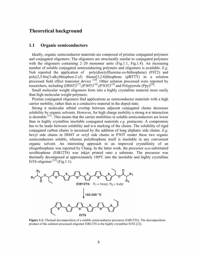
Ideally, organic semiconductor materials are composed of pristine conjugated polymers
and conjugated oligomers. The oligomers are structurally similar to conjugated polymers
with the oligomers containing 2–20 monomer units (Fig.1.1, Fig.1.4). An increasing
number of soluble conjugated semiconducting polymers and oligomers is available. E.g.
Noh reported the application of poly(dioctylfluorene-co-bithiophene) (F8T2) and
poly(2,5-bis(3-alkylthiophen-2-yl) thieno[3,2-b]thiophene (pBTTT) in a solution
processed field effect transistor device [16]
. Other solution processed were reported by
researchers, including (DH4T)[17]
,(P3HT)[18]
,(P3OT)[19]
and Polypyrrole (Ppy)[20]
.
Small molecular weight oligomers form into a highly crystalline material more easily
than high molecular weight polymers.
Pristine conjugated oligomers find applications as semiconductor materials with a high
carrier mobility, rather then as a conductive material in the doped state.
Strong π molecular orbital overlap between adjacent conjugated chains decreases
solubility by organic solvents. However, for high charge mobility a strong π-π interaction
is desirable [21]
. This means that the carrier mobilities in soluble semiconductors are lower
than in highly crystalline insoluble conjugated materials e.g. pentacene. A compromise
has to be made between solubility and π-π stacking of the chains. The solubility of rigid
conjugated carbon chains is increased by the addition of long aliphatic side chains. E.g.
hexyl side chains in DH4T or octyl side chains in P3OT render these two organic
semiconductors soluble, whereas polythiophene itself is insoluble in any convenient
organic solvent. An interesting approach to an improved crystallinity of an
oliogothiophene was reported by Chang. In the latter work, the precursor α,ω-substituted
sexithiophene (EtB12T6) was inkjet printed onto a substrate. The precursor was
thermally decomposed at approximately 180ºC into the insoluble and highly crystalline
EtT6 oligomer [21]
(Fig.1.1).
Figure 1.1: Thermal decomposition of a soluble semiconductor precursor (EtB12T6). The decomposition
product of the solution processed oligomer EtB12T6 is the highly crystalline EtT6 [22].
9
1.1.1 Semiconduction in organic materials
Semiconduction in polymer materials is rather interesting because most polymers are
extremely good electrical insulators. Indeed, polymers are the material type of choice in
the application of electrical cable insulation. What then, does make this class of organic
materials semiconductive? Organic semiconductors share common structure-function
properties, independent of the specific individual materials or their synthesis routes. This
class of materials differs on several key points from classical semiconductors. The next
paragraphs cover the basics of organic semiconductors and illustrates what mechanism
and structures allow the transport of charge carriers through the material.
1.1.2 Conjugation
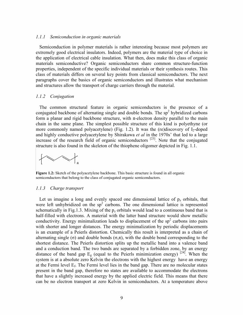
The common structural feature in organic semiconductors is the presence of a
conjugated backbone of alternating single and double bonds. The sp2 hybridized carbons
form a planar and rigid backbone structure, with π-electron density parallel to the main
chain in the same plane. The simplest possible structure of this kind is polyethyne (or
more commonly named polyacetylene) (Fig. 1.2). It was the (re)discovery of I2-doped
and highly conductive polyacetylene by Shirakawa et al in the 1970s’ that led to a large
increase of the research field of organic semiconductors [23]
. Note that the conjugated
structure is also found in the skeleton of the thiophene oligomer depicted in Fig. 1.1.
Figure 1.2: Sketch of the polyacetylene backbone. This basic structure is found in all organic
semiconductors that belong to the class of conjugated organic semiconductors.
1.1.3 Charge transport
Let us imagine a long and evenly spaced one dimensional lattice of pz orbitals, that
were left unhybridized on the sp2 carbons. The one dimensional lattice is represented
schematically in Fig.1.3. Mixing of the pz orbitals would lead to a continuous band that is
half-filled with electrons. A material with the latter band structure would show metallic
conductivity. Energy minimalization leads to displacement of the sp2 carbons into pairs
with shorter and longer distances. The energy minimalization by periodic displacements
is an example of a Peierls distortion. Chemically this result is interpreted as a chain of
alternating single (σ) and double bonds (σ,π), with the double bond corresponding to the
shortest distance. The Peierls distortion splits up the metallic band into a valence band
and a conduction band. The two bands are separated by a forbidden zone, by an energy
distance of the band gap Eg (equal to the Peierls minimization energy) [24]
. When the
system is at a absolute zero Kelvin the electrons with the highest energy have an energy
at the Fermi level Ef. The Fermi level lies in the band gap. There are no molecular states
present in the band gap, therefore no states are available to accommodate the electrons
that have a slightly increased energy by the applied electric field. This means that there
can be no electron transport at zero Kelvin in semiconductors. At a temperature above

10
absolute zero there is an increasing fraction of thermally excited electrons transferred
from the valence band into the conduction band. Both the electrons e- in the conduction
band (N-type) as well as the holes h+ in the valence band (P-type) contribute to the
transport of charge in the ideal material. Only a very small fraction of electrons is
thermally excited into the conduction band at room temperature, to give a free electron
concentration of n. These materials show an intrinsic electrical conductivity that lies
between that of good insulators and that of metals. Electrical conductivity (σ) is a
function of the carrier concentrations (n,p) and the carrier mobility (µ), shown in Eq.1.1.
The mobility is a material property that indicates how easy the charges are accelerated
through the lattice by an applied electrical field.
Σσn = qnµn (1.1)
Pristine organic conjugated materials show both N- and P-type conductivity in
principle, but most organic semiconductors show only hole conductivity because electron
conductivity is suppressed by electron traps. Charge traps occur at defects such as foreign
impurities at grain boundaries or at the interface with the electrodes.
Figure 1.3: Schematic of band formation and consequent band spitting caused by Peierls distortion of an
one-dimensional lattice of carbon sp2 atoms, represented by the black dots in c) and d). The energy ∆E that
is released during the transition corresponds to the band gap Eg. The evenly spaced orbitals of c) would
give rise to the metallic state a). At zero Kelvin the electrons with the highest energy are at the Fermi level
Ef.
1.1.4 Charge carriers
There are several important differences between conventional inorganic
semiconductors and organic semiconductors. Most notably, the charge carrier species
differ from classical inorganic semiconductors. In conventional semiconductors (e.g.
silicon) charges are fully delocalized and do not significantly distort the lattice in their
immediate surrounding. In organic semiconductors, electrons and holes are only
delocalized over a part of the conjugation length (Fig.1.4). The conjugation length is the
undisturbed section of alternating single and double bonds. Short oligomeric materials
show a conjugation length of 2-10 nm which is equal to their molecular length. Polymeric
materials show a wide range of effective conjugation lengths 2->>1 nm, largely
independent of the absolute chain length. The effective conjugation length in polymeric
semiconductors is determined by disorder [24]
(Fig.1.5).
11
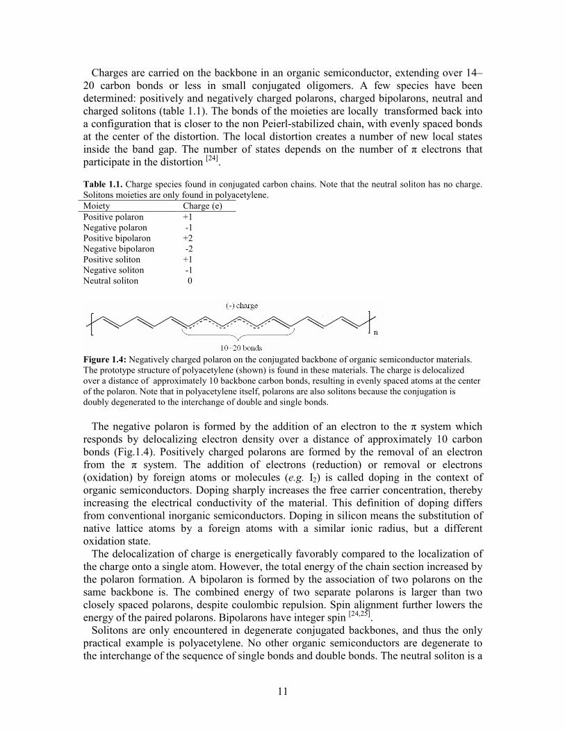
Charges are carried on the backbone in an organic semiconductor, extending over 14–
20 carbon bonds or less in small conjugated oligomers. A few species have been
determined: positively and negatively charged polarons, charged bipolarons, neutral and
charged solitons (table 1.1). The bonds of the moieties are locally transformed back into
a configuration that is closer to the non Peierl-stabilized chain, with evenly spaced bonds
at the center of the distortion. The local distortion creates a number of new local states
inside the band gap. The number of states depends on the number of π electrons that
participate in the distortion [24]
.
Table 1.1. Charge species found in conjugated carbon chains. Note that the neutral soliton has no charge.
Solitons moieties are only found in polyacetylene.
Moiety Charge (e)
Positive polaron +1
Negative polaron -1
Positive bipolaron +2
Negative bipolaron -2
Positive soliton +1
Negative soliton -1
Neutral soliton 0
Figure 1.4: Negatively charged polaron on the conjugated backbone of organic semiconductor materials.
The prototype structure of polyacetylene (shown) is found in these materials. The charge is delocalized
over a distance of approximately 10 backbone carbon bonds, resulting in evenly spaced atoms at the center
of the polaron. Note that in polyacetylene itself, polarons are also solitons because the conjugation is
doubly degenerated to the interchange of double and single bonds.
The negative polaron is formed by the addition of an electron to the π system which
responds by delocalizing electron density over a distance of approximately 10 carbon
bonds (Fig.1.4). Positively charged polarons are formed by the removal of an electron
from the π system. The addition of electrons (reduction) or removal or electrons
(oxidation) by foreign atoms or molecules (e.g. I2) is called doping in the context of
organic semiconductors. Doping sharply increases the free carrier concentration, thereby
increasing the electrical conductivity of the material. This definition of doping differs
from conventional inorganic semiconductors. Doping in silicon means the substitution of
native lattice atoms by a foreign atoms with a similar ionic radius, but a different
oxidation state.
The delocalization of charge is energetically favorably compared to the localization of
the charge onto a single atom. However, the total energy of the chain section increased by
the polaron formation. A bipolaron is formed by the association of two polarons on the
same backbone is. The combined energy of two separate polarons is larger than two
closely spaced polarons, despite coulombic repulsion. Spin alignment further lowers the
energy of the paired polarons. Bipolarons have integer spin [24,25]
.
Solitons are only encountered in degenerate conjugated backbones, and thus the only
practical example is polyacetylene. No other organic semiconductors are degenerate to
the interchange of the sequence of single bonds and double bonds. The neutral soliton is a
12
special case because no charge is carried by the neutral moieties. A change in the
sequence of singe-double bonds at the location of the neutral soliton gives rise to a
delocalized radical, similar to the delocalization of the polaron moieties but without
charge.
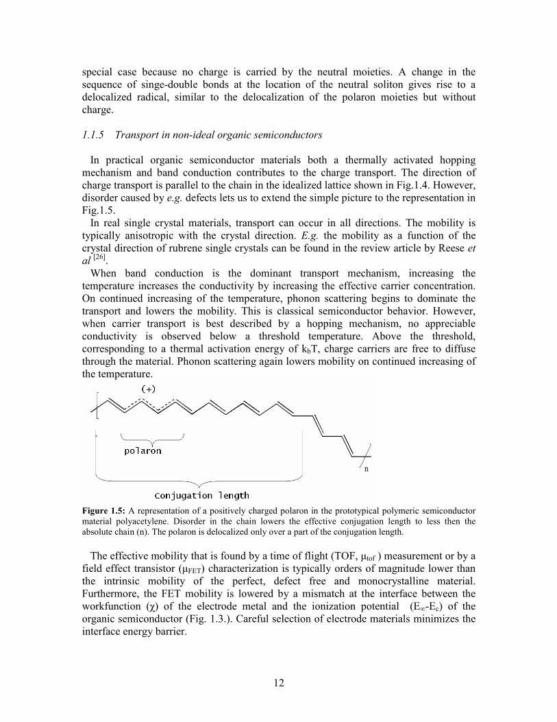
1.1.5 Transport in non-ideal organic semiconductors
In practical organic semiconductor materials both a thermally activated hopping
mechanism and band conduction contributes to the charge transport. The direction of
charge transport is parallel to the chain in the idealized lattice shown in Fig.1.4. However,
disorder caused by e.g. defects lets us to extend the simple picture to the representation in
Fig.1.5.
In real single crystal materials, transport can occur in all directions. The mobility is
typically anisotropic with the crystal direction. E.g. the mobility as a function of the
crystal direction of rubrene single crystals can be found in the review article by Reese et
al [26]
.
When band conduction is the dominant transport mechanism, increasing the
temperature increases the conductivity by increasing the effective carrier concentration.
On continued increasing of the temperature, phonon scattering begins to dominate the
transport and lowers the mobility. This is classical semiconductor behavior. However,
when carrier transport is best described by a hopping mechanism, no appreciable
conductivity is observed below a threshold temperature. Above the threshold,
corresponding to a thermal activation energy of kbT, charge carriers are free to diffuse
through the material. Phonon scattering again lowers mobility on continued increasing of
the temperature.
Figure 1.5: A representation of a positively charged polaron in the prototypical polymeric semiconductor
material polyacetylene. Disorder in the chain lowers the effective conjugation length to less then the
absolute chain (n). The polaron is delocalized only over a part of the conjugation length.
The effective mobility that is found by a time of flight (TOF, µtof ) measurement or by a
field effect transistor (µFET) characterization is typically orders of magnitude lower than
the intrinsic mobility of the perfect, defect free and monocrystalline material.
Furthermore, the FET mobility is lowered by a mismatch at the interface between the
workfunction (χ) of the electrode metal and the ionization potential (E∞-Ec) of the
organic semiconductor (Fig. 1.3.). Careful selection of electrode materials minimizes the
interface energy barrier.
13
Grain boundaries in polycrystalline organic materials introduce another extra barrier to
FET carrier mobility. The contribution of the grain boundaries to the total energy barrier
is a function of the number of grain boundaries. The grain boundaries are passed by the
carriers traveling between the electrodes. Large crystallite size compared to the electrode-
electrode distance minimizes the grain boundary influence. Other defects e.g. impurities,
further lower mobility. In general any defect type lowers the mobility by introducing
extra disorder (Eq.1.2).
1/µeffective = 1/µintrinsic + 1/µgrain boundary + 1/µelectrodes + 1/µm + 1/µm+1 + .. + 1/µM (1.2)
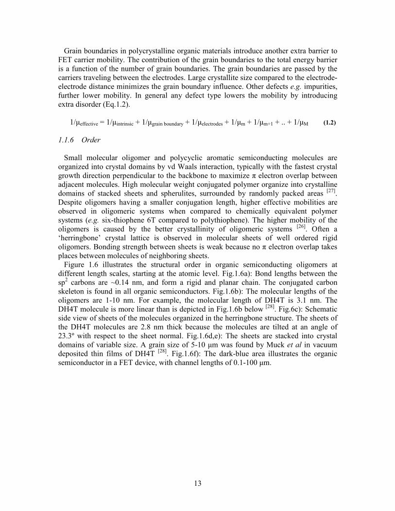
1.1.6 Order
Small molecular oligomer and polycyclic aromatic semiconducting molecules are
organized into crystal domains by vd Waals interaction, typically with the fastest crystal
growth direction perpendicular to the backbone to maximize π electron overlap between
adjacent molecules. High molecular weight conjugated polymer organize into crystalline
domains of stacked sheets and spherulites, surrounded by randomly packed areas [27]
.
Despite oligomers having a smaller conjugation length, higher effective mobilities are
observed in oligomeric systems when compared to chemically equivalent polymer
systems (e.g. six-thiophene 6T compared to polythiophene). The higher mobility of the
oligomers is caused by the better crystallinity of oligomeric systems [26]
. Often a
‘herringbone’ crystal lattice is observed in molecular sheets of well ordered rigid
oligomers. Bonding strength between sheets is weak because no π electron overlap takes
places between molecules of neighboring sheets.
Figure 1.6 illustrates the structural order in organic semiconducting oligomers at
different length scales, starting at the atomic level. Fig.1.6a): Bond lengths between the
sp2 carbons are ~0.14 nm, and form a rigid and planar chain. The conjugated carbon
skeleton is found in all organic semiconductors. Fig.1.6b): The molecular lengths of the
oligomers are 1-10 nm. For example, the molecular length of DH4T is 3.1 nm. The
DH4T molecule is more linear than is depicted in Fig.1.6b below [28]
. Fig.6c): Schematic
side view of sheets of the molecules organized in the herringbone structure. The sheets of
the DH4T molecules are 2.8 nm thick because the molecules are tilted at an angle of
23.3º with respect to the sheet normal. Fig.1.6d,e): The sheets are stacked into crystal
domains of variable size. A grain size of 5-10 µm was found by Muck et al in vacuum
deposited thin films of DH4T [28]
. Fig.1.6f): The dark-blue area illustrates the organic
semiconductor in a FET device, with channel lengths of 0.1-100 µm.
14
Figure 1.6: Order in organic semiconductor materials, starting at the nanometer scale of molecules a) up to
the micrometer scale length scale of f) devices.
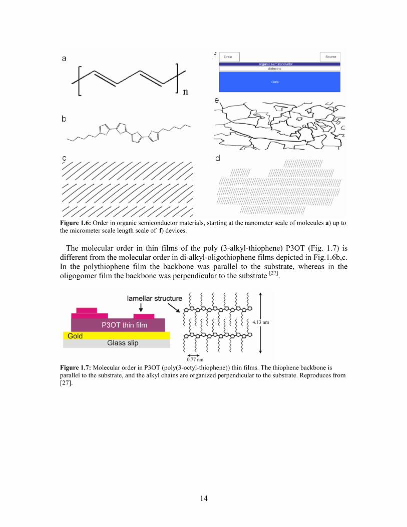
The molecular order in thin films of the poly (3-alkyl-thiophene) P3OT (Fig. 1.7) is
different from the molecular order in di-alkyl-oligothiophene films depicted in Fig.1.6b,c.
In the polythiophene film the backbone was parallel to the substrate, whereas in the
oligogomer film the backbone was perpendicular to the substrate [27]
.
Figure 1.7: Molecular order in P3OT (poly(3-octyl-thiophene)) thin films. The thiophene backbone is
parallel to the substrate, and the alkyl chains are organized perpendicular to the substrate. Reproduces from
[27].

15
1.2 Pentacene
Figure 1.8(a) shows the molecular structure of pentacene (C22H14). Then, at a larger
length scale, figure 1.8(b) shows multiple pentacene molecules stacked in the so called
herringbone crystal packing. Next, figure 1.8(c) shows a pentacene single crystal at an
even larger length scale. The individual molecules cannot longer be seen in the image.
These images show the idealized model of a defect free, high purity, single crystal of
pentacene. Although real pentacene single crystals are not nearly as perfect as shown in
image of figure 1.8, it is a useful starting model. The simplistic model can be extended
with the incorporation of defects (e.g. impurities, strain) to better approach the realistic
situation.
Figure 1.8(a): Pentacene molecular structure, C22H14.
Figure 1.8(b): Pentacene crystal packing with the characteristic herringbone structure in the a-b crystal
direction. Modified from [31].
Figure 1.8(c): Model of a pentacene single crystal. The a-b crystal direction is indicated by the red and
green arrows, the c crystal direction is indicated by the blue arrow.
Pentacene is the fifth in the aromatic series starting with benzene, naphthalene,
anthracene and tetracene. The molecular chemistry is related to both the aromatic parent
compound benzene and, at the other end of the scale, to a single sheet of graphite
(graphene). Structurally, pentacene behaves analogue to other the molecular organic
semiconductor compounds, such as the class of short thiophenes (e.g. Fig. 1.1).
16
Pentacene thin films are primarily deposited by a thermal evaporation technique[30]
. A
number of other techniques have been developed in literature for the deposition of
pentacene thin films or single crystals. Notably, molecular beam deposition (MBD) is
currently intensely studied as a means of kinetic controlling the growth of the pentacene
thin layers[31-35]
. Yet another, but not yet widely adopted method, is pulsed laser
deposition (PLD) of thin film pentacene. PLD potentially allow for a well controlled
kinetics of the pentacene layer growth[36-41]
.
Practical issues make the fabrication of electrodes and dielectrics on single crystals
challenging. Pentacene single crystal field effect transistors have been fabricated in
literature in two main ways: by directly patterning the source/drain and gate(dielectric)
structure onto the surface of the single crystal, or by the ‘flip crystal’ method. In the last
method, the single crystal is positioned onto a ready-made source/drain gate(dielectric)
structure and held in place by electrostatic forces. Both traditional metal-oxide based
dielectrics as well as organic (e.g. parylene) dielectric materials have been used.
Many groups have used Ag-epoxy or graphite-epoxy electrodes. These devices showed
problems such as ‘flicker’ noise [42]
in the IV data, or showed a large IV hysteresis in the
IV curve. The hysteresis effect means the IV curve is different when the current goes
from source to drain or drain to source respectively.
Pentacene is typically characterized as a P-type organic semiconductor. However, an
ultra pure, defect-free specimen of pentacene would show its intrinsic conductivity to be
originating from both free holes as well as free electrons. The normally observed absence
of significant electron conductivity is due to fixation, or trapping, of these negatively
charged electrons.
1.2.1 Single crystal pentacene
As mentioned earlier, single crystal pentacene is commonly selected in literature to
study the intrinsic properties of the pentacene system. Using single crystals effectively
eliminates grain boundary interfaces. Although the elimination of grain boundary
influences is a good first step, other interfaces play an equally important role during the
electrical characterization.
Figure 1.9 shows an optical photograph of an as-received pentacene single crystal.
Pentacene single crystals can be as large as 10x5 mm with ~ 20 µm thickness. The single
crystals have a dark blue appearance, fading into a dark purple when the crystals get very
thin. It was visible under the polarized lights of a optical microscope that the single
crystals were in fact composed of several large, mm-sized grains in most investigated
crystals.

17
Figure 1.9(a): Pentacene single crystal on a silicon substrate. A silver particle suspension glue was used to
secure the crystal in place, the glue is visible in the top left and bottom right in the picture. The crystal
width is approximately 1 mm. The diagonal features indicate that the top surface is not perfectly aligned to
the a-b direction; a perfect alignment would not show such features. The brighter colored squares and
circles are Au electrodes deposited by pulsed laser deposition on the pentacene surface. (b) SEM image of
the same sample.
As mentioned, single crystal pentacene is commonly selected by researchers to study
the intrinsic properties of the pentacene system[4]
. Using single crystals effectively
eliminates grain boundary interfaces. But quite independently of the bulk characteristics
of the crystals, it is the surface of the pentacene crystals that is important for the intended
application in field effect transistors.
The elimination of grain boundary influences is a good first step, however, other factors
play an important role during the electrical characterization. The other factors that have a
impact on the electrical characteristics of single crystals pentacene include: impurities,
adsorbed gasses (e.g. O2, N2), adsorbed water vapor, reaction products (e.g. by photo
catalyzed oxidation), fabrication techniques and the materials used.
The focus in this work lies with the oxidation product of pentacene: 6,13-
pentacenequinone (PenQ, C22H12O2). The overall reaction with water as the other product
is shown in Eq. 1.3. The detection of PenQ on the crystals is caused either by oxidation
after the crystals have been grown or is caused by the co-deposition of PenQ from an
impure pentacene source.
Hν,air
C22H14 + 3O2 ���� C22H12 + 2H2O (Eq. 1.3)
Jurchescu et al reported the electrical characteristics of single crystal pentacene,
influenced by the diffusion of air (ambient and dry) into the single crystals. In their 2005
paper, thermo gravimetric analysis (TGA) at room temperature and atmospheric pressure
was applied to monitor the mass change. After 5 hours (300 min) the sample mass
increased by approximately 2.0%, not depending on the gas used (O2, N2, Ar).
The intercalated water causes trapping of injected charges. The water-induced traps
lower the electrical conductivity by decreasing the number of free carriers and increasing
the energetic disorder. The opposite effect is observed on the absorption of O2 molecules
into the pentacene crystals. It is likely that the electronegative oxygen is able to increase
18
the conductivity by increasing the free carrier concentration. The pentacene molecules
donate electron density to the oxygen, thereby forming electron holes.
Additionally, in their work of 2005, they performed the identical experiment in the dark
and under illumination by fluorescent light. The experiment showed an increase in the
electrical conductivity of the samples, when compared to the dark measurement. No
apparent chemical reactions were observed in their samples, tested under any of the
experimental conditions. The samples could be brought back to the starting weight. The
electrical characteristics were reversible as well.
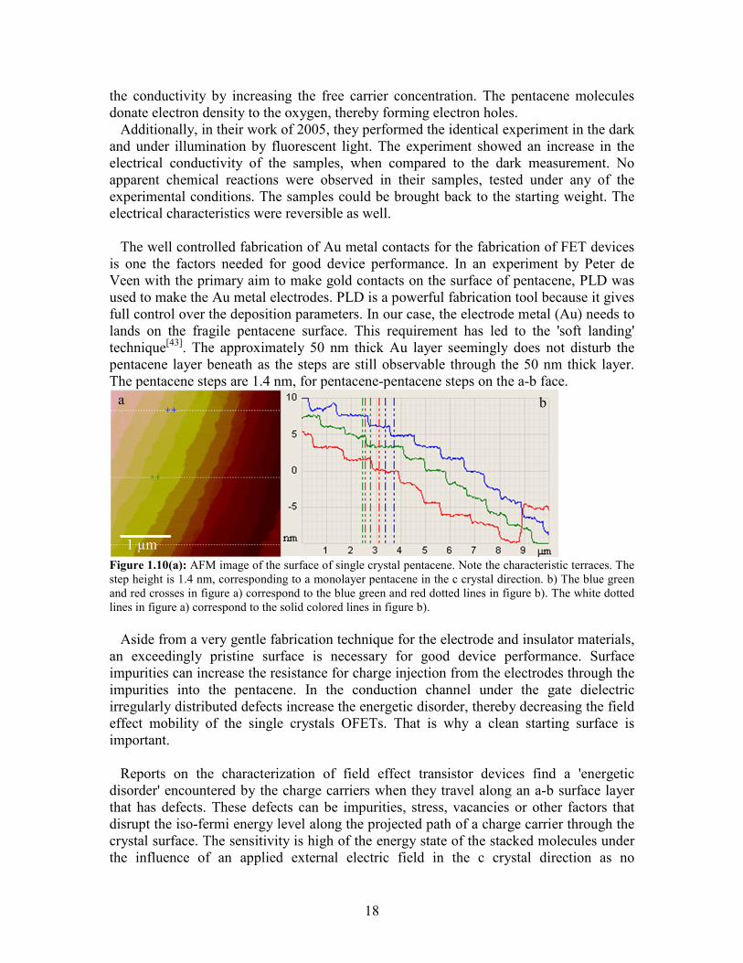
The well controlled fabrication of Au metal contacts for the fabrication of FET devices
is one the factors needed for good device performance. In an experiment by Peter de
Veen with the primary aim to make gold contacts on the surface of pentacene, PLD was
used to make the Au metal electrodes. PLD is a powerful fabrication tool because it gives
full control over the deposition parameters. In our case, the electrode metal (Au) needs to
lands on the fragile pentacene surface. This requirement has led to the 'soft landing'
technique[43]
. The approximately 50 nm thick Au layer seemingly does not disturb the
pentacene layer beneath as the steps are still observable through the 50 nm thick layer.
The pentacene steps are 1.4 nm, for pentacene-pentacene steps on the a-b face.
Figure 1.10(a): AFM image of the surface of single crystal pentacene. Note the characteristic terraces. The
step height is 1.4 nm, corresponding to a monolayer pentacene in the c crystal direction. b) The blue green
and red crosses in figure a) correspond to the blue green and red dotted lines in figure b). The white dotted
lines in figure a) correspond to the solid colored lines in figure b).
Aside from a very gentle fabrication technique for the electrode and insulator materials,
an exceedingly pristine surface is necessary for good device performance. Surface
impurities can increase the resistance for charge injection from the electrodes through the
impurities into the pentacene. In the conduction channel under the gate dielectric
irregularly distributed defects increase the energetic disorder, thereby decreasing the field
effect mobility of the single crystals OFETs. That is why a clean starting surface is
important.
Reports on the characterization of field effect transistor devices find a 'energetic
disorder' encountered by the charge carriers when they travel along an a-b surface layer
that has defects. These defects can be impurities, stress, vacancies or other factors that
disrupt the iso-fermi energy level along the projected path of a charge carrier through the
crystal surface. The sensitivity is high of the energy state of the stacked molecules under
the influence of an applied external electric field in the c crystal direction as no
a b
1 µm

19
significant hybridization of adjacent molecules takes place in the c direction. As a result,
no molecular band is formed in the c direction. Hybridization and band formation does
occur in the a-b direction however, as was reported in literature.
1.2.2 6,13-pentacenequinone on pentacene single crystals
The above mentioned factors that have an impact on the electrical performance, are not
necessarily distributed homogenously throughout the pentacene single crystals. The
defects at, or close to, the surface will have the greatest effect of these electrical
properties, and yet, it is the surface that shows the presence of increased concentration of
the oxidation impurity 6,13-pentacenequinone. Jurchescu et al reported an elegant way to
incorporate the surface impurities into the dielectric layer of a field effect transistor by
selecting 6,13-pentacenequinone as the dielectric layer. The FET devices showed a field
effect mobility approaching values that are normally only found in space charge limited
(SCLC) mobility measurements.
Both non-ohmic contacts as well as ohmic contacts were observed in work by de
Veen[44]
in an apparently similar system, raising questions on the origins of the observed
discrepancies.
A layer of PenQ can form an insulating surface layer, as was shown in work of
Jurchescu[45]
. For good electrical contacts, and therefore good devices, a clean pentacene
surface is needed. The surface of the pentacene crystals play a critical role during the
characterization of electrical properties when devices are fabricated on the surface of
these crystals. Irregular surface layers of PenQ cause an increase of the contact resistance
of metal-pentacene contacts.
Fig 1.11: 6,13-pentacenequinone molecular structure, C22H12O2.
Figure 1.12: Pentacene single crystal with Au contacts on a silicon substrate. A silver particle suspension
glue was used to secure the crystal in place, the glue is visible in the top left and bottom right in the picture.
The crystal width is approximately 1 mm.
It is our hypothesis that a significant fraction of 6,13-pentacenequinone is present on
the surface of the pentacene single crystals, even though the overall bulk purity is far

20
better than the purity of commercial pentacene powders. In such a scenario, 6,13-
pentacenequinone would be found at the pentacene-pentacene and pentacene-gas grain
boundaries as the crystals are grown. This first mechanism is based on the principle that
PenQ molecules do not get built into the growing lattice as easily as the pentacene
molecules. See figure 1.13 for a overview of the physical vapor deposition process used
for the growth of pentacene single crystals. Pentacene is synthesized by using 6,13-
pentacenequinone as the precursor and this ends up partially in the pentacene powders,
and finally, single crystals. During crystal growth a proportionally large fraction of the
impurities is deposited onto the surface, which then again can sublimate and crystallize
further along the crystallization tube. Any PenQ that does stay behind on the pentacene
single crystal surface is likely to adopt the bulk phase crystalline structure.
Figure 1.13: Physical vapor deposition setup for the growth of pentacene single crystals with Ar as the
carrier gas. a) Pentacene powder source powder. b) deposition location of the pentacene single crystals
inside the quartz tube. c) Location of the deposited 6,13-pentacenequinone impurity. The grey tube is
surrounded by a heating coil (yellow color) which is wound at a higher coil density at the point of the
pentacene powder source.
Figure 1.14(a): SEM image showing surface patches on a pentacene single crystal. b) AFM image
showing surface patches of PenQ on a pentacene single crystal.
The second mechanism to explain the presence of PenQ on the pentacene surface, is the
oxidation of the pentacene molecular layers that are exposed to light and oxygen from air
after the crystals are grown. Pentacene molecules are oxidized, forming a
pentacenequinone molecular layer. Bulk PenQ crystallizes in 1.779 nm think layers,
a b
Ar gas a
b
c
21
consisting of two alternating PenQ monolayers. PenQ monolayers are thinner (0.89 nm)
then pentacene monolayers (1.41nm).
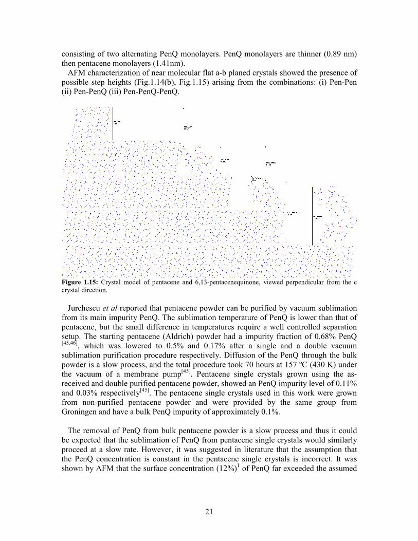
AFM characterization of near molecular flat a-b planed crystals showed the presence of
possible step heights (Fig.1.14(b), Fig.1.15) arising from the combinations: (i) Pen-Pen
(ii) Pen-PenQ (iii) Pen-PenQ-PenQ.
Figure 1.15: Crystal model of pentacene and 6,13-pentacenequinone, viewed perpendicular from the c
crystal direction.
Jurchescu et al reported that pentacene powder can be purified by vacuum sublimation
from its main impurity PenQ. The sublimation temperature of PenQ is lower than that of
pentacene, but the small difference in temperatures require a well controlled separation
setup. The starting pentacene (Aldrich) powder had a impurity fraction of 0.68% PenQ [45,46]
, which was lowered to 0.5% and 0.17% after a single and a double vacuum
sublimation purification procedure respectively. Diffusion of the PenQ through the bulk
powder is a slow process, and the total procedure took 70 hours at 157 ºC (430 K) under
the vacuum of a membrane pump[45]
. Pentacene single crystals grown using the as-
received and double purified pentacene powder, showed an PenQ impurity level of 0.11%
and 0.03% respectively[45]
. The pentacene single crystals used in this work were grown
from non-purified pentacene powder and were provided by the same group from
Groningen and have a bulk PenQ impurity of approximately 0.1%.
The removal of PenQ from bulk pentacene powder is a slow process and thus it could
be expected that the sublimation of PenQ from pentacene single crystals would similarly
proceed at a slow rate. However, it was suggested in literature that the assumption that
the PenQ concentration is constant in the pentacene single crystals is incorrect. It was
shown by AFM that the surface concentration (12%)1 of PenQ far exceeded the assumed
22
bulk purity (0.03%), whereas no surface PenQ could be detected by the AFM method on
an freshly exposed crystal interface[46]
.
1 The surface concentration was calculated from the ratio of the number of PenQ step-heights compared to
the number of pentacene step-heights as measured by AFM [46]
.
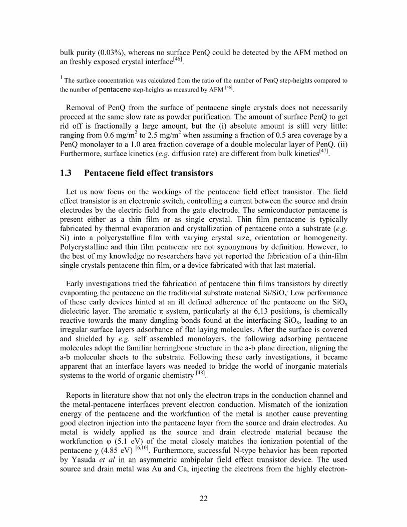
Removal of PenQ from the surface of pentacene single crystals does not necessarily
proceed at the same slow rate as powder purification. The amount of surface PenQ to get
rid off is fractionally a large amount, but the (i) absolute amount is still very little:
ranging from 0.6 mg/m2 to 2.5 mg/m
2 when assuming a fraction of 0.5 area coverage by a
PenQ monolayer to a 1.0 area fraction coverage of a double molecular layer of PenQ. (ii)
Furthermore, surface kinetics (e.g. diffusion rate) are different from bulk kinetics[47]
.
1.3 Pentacene field effect transistors
Let us now focus on the workings of the pentacene field effect transistor. The field
effect transistor is an electronic switch, controlling a current between the source and drain
electrodes by the electric field from the gate electrode. The semiconductor pentacene is
present either as a thin film or as single crystal. Thin film pentacene is typically
fabricated by thermal evaporation and crystallization of pentacene onto a substrate (e.g.
Si) into a polycrystalline film with varying crystal size, orientation or homogeneity.
Polycrystalline and thin film pentacene are not synonymous by definition. However, to
the best of my knowledge no researchers have yet reported the fabrication of a thin-film
single crystals pentacene thin film, or a device fabricated with that last material.
Early investigations tried the fabrication of pentacene thin films transistors by directly
evaporating the pentacene on the traditional substrate material Si/SiOx. Low performance
of these early devices hinted at an ill defined adherence of the pentacene on the SiOx
dielectric layer. The aromatic π system, particularly at the 6,13 positions, is chemically
reactive towards the many dangling bonds found at the interfacing SiOx, leading to an
irregular surface layers adsorbance of flat laying molecules. After the surface is covered
and shielded by e.g. self assembled monolayers, the following adsorbing pentacene
molecules adopt the familiar herringbone structure in the a-b plane direction, aligning the
a-b molecular sheets to the substrate. Following these early investigations, it became
apparent that an interface layers was needed to bridge the world of inorganic materials
systems to the world of organic chemistry [48]
.
Reports in literature show that not only the electron traps in the conduction channel and
the metal-pentacene interfaces prevent electron conduction. Mismatch of the ionization
energy of the pentacene and the workfuntion of the metal is another cause preventing
good electron injection into the pentacene layer from the source and drain electrodes. Au
metal is widely applied as the source and drain electrode material because the
workfunction φ (5.1 eV) of the metal closely matches the ionization potential of the
pentacene χ (4.85 eV) [6,10]
. Furthermore, successful N-type behavior has been reported
by Yasuda et al in an asymmetric ambipolar field effect transistor device. The used
source and drain metal was Au and Ca, injecting the electrons from the highly electron-
23
donating calcium electrode [49]
. Using this scheme, the ionization potential of the
pentacene is effectively shifted to a less oxidizing state with respect to the electrode
material. Similarly, using the highly electronegative fluor-pentacene (all hydrogen atoms
replaced by fluor atoms) also led to a N-type device, this time by shifting the organic
semiconductor to a more oxidizing state, enabling the transition of an electron from the
Au electrode into the fluor-pentacene matrix. An interesting application of self assembled
monolayers was reported by Calhoun et al. They reacted a very chemically reactive self
assembly monolayer (SAM) compound with an R-SiCl3 (chlorosilane) end group. The
chlorosilane group is reactive enough to receive electron density from the top pentacene
layer, rendering the pentacene top layer electrically conductive. The group led by
Calhoun et al showed that they could increase the surface concentration of charge carriers
to 3·1023
cm-2
, approaching the density in an opened channel in OFET devices [48]
.
The two most common FET architectures in organic thin film transistors are top gate
and bottom gate electrode geometries. Furthermore, the design either has top or bottom
source and drain electrodes (or a combination, e.g. up drain and bottom source).
Single pentacene FETs are often fabricated by the ‘flipped crystal’ method, for practical
convenience. Source and drain electrodes in the latter designs are usually Au or other
metal contact, fabricated by e.g. photo lithographical means. The gate electrode typically
consists of a doped silicon substrate, with SiOx or other insulating material acting as the
gate dielectric.
The measured total electrical resistance in a field effect transistor is composed of
several components: the channel resistance and the contact resistance at the source and
drain electrodes. The channel resistance and the contact resistance are convoluted in the
total resistance of a typical pentacene fields effect transistor. Recognizing the importance
of the components contributing to the resistance, Yagi et al, developed a method to
differentiate the individual contributions of total resistance [50]
. In their work, they
describe the fabrication and characterization of a four terminal thin film transistor by a
computer-controlled pulsed laser ablation (532 nm) technique of a 30 nm thick pentacene
thin-film on a SiO2/Si substrate.
Although thin-film applications of pentacene do not give the same control over the
investigated systems, it often sufficient for the targeted commercial applications.
Industrial applications do not require the same level of control as fundamental research.
The thin-films of pentacene are polycrystalline, and are typically fabricated by a thermal
evaporation technique, with the two important exceptions of molecular beam deposition
and pulsed laser deposition [37-41, 51,52]
.

24
2 Experimental
2.1 Equipment
2.1.1 Nanomanipulator system
SEM images were taken with the JEOL 6490 scanning electron microscope. The
scanning electron microscope is part of the nanomanipulator setup, further composed of
the Keithley 4200 source measure unit and the Zyvex s100 Nanoprober. The
nanomanipulator system is designed for nano-scale electrical characterization and
mechanical manipulation.
2.1.2 Pulsed laser deposition system
The pulsed laser deposition system consisted of a vacuum chamber with optical
window, a target of the deposition material, a sample holder with heater and a lens
system to direct the pulsed laser radiation from a LPX2000 KrF excimer laser (248 nm
25ns) to the target. The heater in the system was used to heat the pentacene samples in a
vacuum [53]
.
2.2 Pentacene single crystal surface characterization
2.2.1 Characterization by SEM
The Pentacene single crystals were kindly supplied by the Solid State Chem Lab,
University Groningen of the group led by Palstra.
As mentioned, 6,13-pentacenequinone (PenQ) is found as the main impurity in
commercial pentacene powder as well as in carefully grown single crystals [4,15,45,58,59,54-
56]. Other impurities with a lower concentration include 6,13-pentacenehydrides and
peripentacenes with the latter formed by linking multiple pentacene molecules together,
when the crystals are grown under a reducing atmosphere [57]
. Although the fraction of
PenQ is much less then what is found in the starting bulk powders: (i) it only takes a very
small fraction of impurities to significantly alter the electric properties of pentacene,
depending on the identity of the impurity. (ii) PenQ functions as a charge trap in the
pentacene system. (iii) During pentacene single crystal growth, the PenQ is not
distributed homogeneously, but is likely deposited largely on the surface of the crystal, as
was also suggested in recent literature [e.g. 15,55]
.
The pentacene single crystals were investigated using an electron microscope set at a
low electron acceleration setting.
25
2.2.2 Atomic force microscopy
AFM measurement of the pentacene samples were performed by Peter de Veen, IMS
group, University of Twente.
2.3 Heat treatment of pentacene single crystals
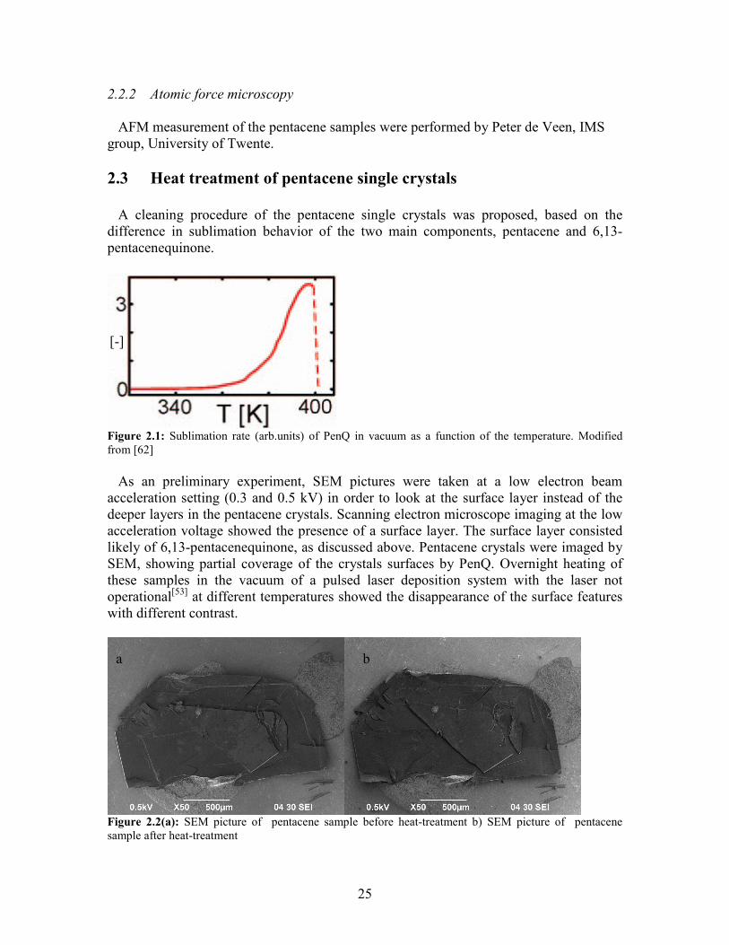
A cleaning procedure of the pentacene single crystals was proposed, based on the
difference in sublimation behavior of the two main components, pentacene and 6,13-
pentacenequinone.
Figure 2.1: Sublimation rate (arb.units) of PenQ in vacuum as a function of the temperature. Modified
from [62]
As an preliminary experiment, SEM pictures were taken at a low electron beam
acceleration setting (0.3 and 0.5 kV) in order to look at the surface layer instead of the
deeper layers in the pentacene crystals. Scanning electron microscope imaging at the low
acceleration voltage showed the presence of a surface layer. The surface layer consisted
likely of 6,13-pentacenequinone, as discussed above. Pentacene crystals were imaged by
SEM, showing partial coverage of the crystals surfaces by PenQ. Overnight heating of
these samples in the vacuum of a pulsed laser deposition system with the laser not
operational[53]
at different temperatures showed the disappearance of the surface features
with different contrast.
Figure 2.2(a): SEM picture of pentacene sample before heat-treatment b) SEM picture of pentacene
sample after heat-treatment
[-]
a b

26
Atomic force microscopy data showed step sizes consistent with the presence of
pentacene steps in the c direction, as well as PenQ monolayers. AFM showed that the
PenQ had disappeared after the heat treatments, but AFM also showed that the
temperature range for removal of the PenQ is narrow. At too high temperature, and with
too long heating of the samples the pentacene surface is changed significantly as the
pentacene is beginning to sublimate itself as well under these conditions (See ch.3.). The
AFM measurements were done by Peter de Veen [44]
.
Figure 2.3(a): AFM image from the surface of a pentacene single crystal before heating in vacuum. b)
AFM image from the surface of a pentacene single crystal after heating (70°C) in vacuum [44].
2.4 In situ heat treatment
2.4.1 SEM image processing
Optical and electron microscope imaging techniques are widely applied in research
because these techniques give fast and visual results. However, the interpretation of the
images typically yields qualitive information. Getting quantative information from a
sequence of images through image processing is rarely performed, although in recent
years good image processing software has begun to appear on the market.
As mentioned, it was observed by SEM that surface features disappeared at elevated
temperatures under vacuum. The image sequences taken at different temperatures give
information on the sublimation rate of the surface layer. A characterization procedure
was developed to quantitively monitor the surface of the pentacene single crystals while
they were being heated inside the scanning electron microscope.
The analysis procedure starts with an image sequence of the surface area of the
pentacene crystals at a specific temperature, at different time intervals. The images show
the surface of a pentacene crystal. Pentacene is indicated by the dark grey color, and
6,13-pentacenequinone is indicated by the lighter shade of grey. Very dark or very light
regions are caused by shadows or oversaturation of the electron detector caused by e.g.
obstruction and reflections. These regions do not change over time and can therefore be
differentiated from the pentacene and sublimating surface features. The contrast between
the light and dark grey value is too low to make a quantative analysis without image
processing.
1 µm 1 µm
27
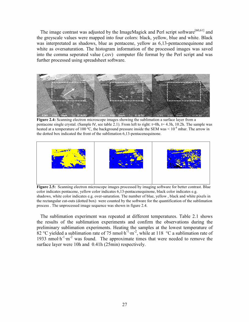
The image contrast was adjusted by the ImageMagick and Perl script software[60,61]
and
the greyscale values were mapped into four colors: black, yellow, blue and white. Black
was interpretated as shadows, blue as pentacene, yellow as 6,13-pentacenequinone and
white as oversaturation. The histogram information of the processed images was saved
into the comma seperated value (.csv) computer file format by the Perl script and was
further processed using spreadsheet software.
Figure 2.4: Scanning electron microscope images showing the sublimation a surface layer from a
pentacene single crystal. (Sample IV, see table 2.1). From left to right: t=0h, t= 4.3h, 10.2h. The sample was
heated at a temperature of 100 ºC, the background pressure inside the SEM was < 10-4
mbar. The arrow in
the dotted box indicated the front of the sublimation 6,13-pentacenequinone.
Figure 2.5: Scanning electron microscope images processed by imaging software for better contrast. Blue
color indicates pentacene, yellow color indicates 6,13-pentacenequinone, black color indicates e.g.
shadows, white color indicates e.g. over-saturation. The number of blue, yellow , black and white pixels in
the rectangular cut-outs (dotted box) were counted by the software for the quantification of the sublimation
process . The unprocessed image sequence was shown in figure 2.4.
The sublimation experiment was repeated at different temperatures. Table 2.1 shows
the results of the sublimation experiments and confirm the observations during the
preliminary sublimation experiments. Heating the samples at the lowest temperature of
82 °C yielded a sublimation rate of 75 nmol·h-1
·m-2
, while at 118 °C a sublimation rate of
1933 nmol·h-1
·m-2
was found. The approximate times that were needed to remove the
surface layer were 10h and 0.41h (25min) respectively.

28
Table 2.1: Sample data and sublimation rate calculated from the scanning electron microscope image
sequences.
Sample T Sublimation rate Sublimation rate
ºC -m-2
·h-1
·m-2
-10-9
·mol·h-1
·m-2
I 82 0.018 75 II 88 0.070 289 III 91 0.245 1005 IV 100 0.072 296 V 118 0.471 1933
Note: The sublimation rate in the third column is the actual measured sublimation rate; it is expressed in the
rate of disappearing surface area. The sublimation rate in the fourth column assumes a monolayer coverage
of 6,13-pentacenequinone.

29
3 Results and discussion
3.1 Pentacene single crystal surface
3.1.1 Characterization by SEM
Scanning electron microscope images showed the presence of a thin surface layer. The
thin surface layer was only visible by using an low electron beam acceleration energy.
(See also Ch.2.4).
Figure 3.0: Scanning electron microscope image of a pentacene single crystal at a low (0.5 keV) electron
beam acceleration energy. The inset show a magnification of the surface to show the irregular shaped
patches of 6,13-pentacenequinone.
3.1.2 Characterization by AFM
The as-received crystals were characterized with atomic force microscopy (AFM) by
Peter de Veen[44]
. Normal AFM height images (Fig 3.1(a) and Fig 3.1(c)) and AFM
image is shown below (Fig. 3.1(b). The SEM results combined with the AFM
measurements (height and phase data) indicate that the thin surface layer is a monolayer
6,13-pentacenequinone.
The height images showed step heights on the pentacene single crystal surface
corresponding to Pen-Pen, Pen-PenQ monolayers and Pen-PenQ double layers (see Fig.
1.15). In bulk crystalline PenQ the stacking of subsequent unit-cell layers in the c
direction normally shows steps consisting of two PenQ molecular layers, alternating with
its molecular axis between +φº or -φº from the c directional axis (Fig. 3.1). The latter
work by de Veen confirms that the surface shows irregular patches of PenQ. The phase
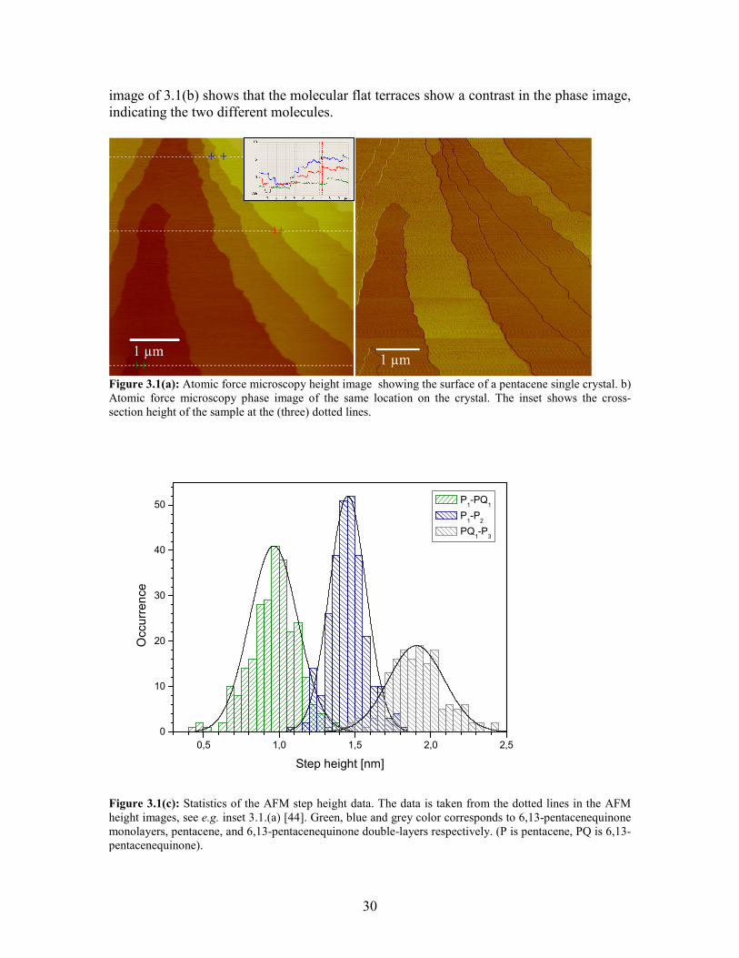
30
image of 3.1(b) shows that the molecular flat terraces show a contrast in the phase image,
indicating the two different molecules.
Figure 3.1(a): Atomic force microscopy height image showing the surface of a pentacene single crystal. b)
Atomic force microscopy phase image of the same location on the crystal. The inset shows the cross-
section height of the sample at the (three) dotted lines.
0,5 1,0 1,5 2,0 2,5
0
10
20
30
40
50
Occu
rre
nce
Step height [nm]
P1-PQ
1
P1-P
2
PQ1-P
3
Figure 3.1(c): Statistics of the AFM step height data. The data is taken from the dotted lines in the AFM
height images, see e.g. inset 3.1.(a) [44]. Green, blue and grey color corresponds to 6,13-pentacenequinone
monolayers, pentacene, and 6,13-pentacenequinone double-layers respectively. (P is pentacene, PQ is 6,13-
pentacenequinone).
1 µm 1 µm
31
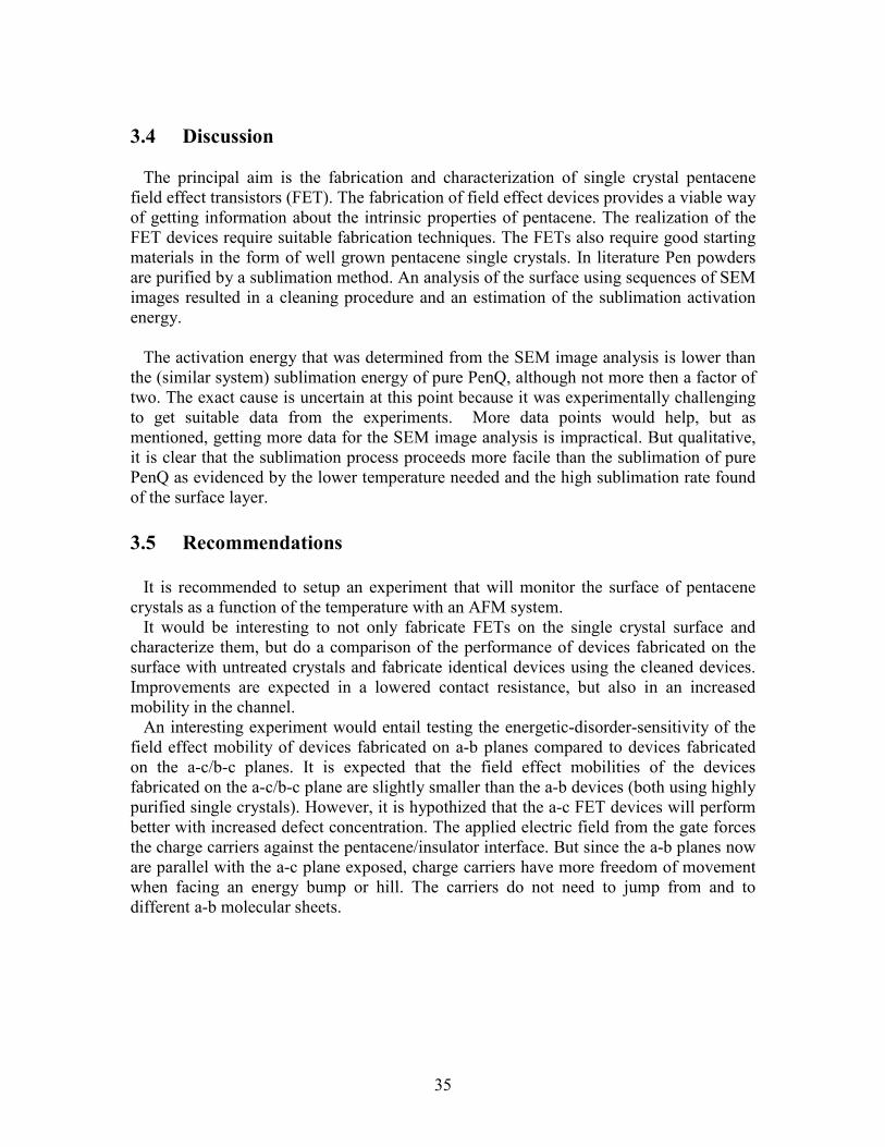
3.2 Heat treated pentacene single crystals
Although the heating procedure of the samples can take a very short time at high
temperatures, it is not well controlled. Uncontrolled heating at too high temperature or
too long duration leads to the degradation of the pentacene surface because the pentacene
begins to sublimate from the surface, leaving behind features resembling potholes. Figure
3.2 shows the pit formation as imaged by AFM. Since the sublimation of pentacene and
6,13-pentacenequinone takes place under near identical conditions, a slow surface
treatment is preferred.
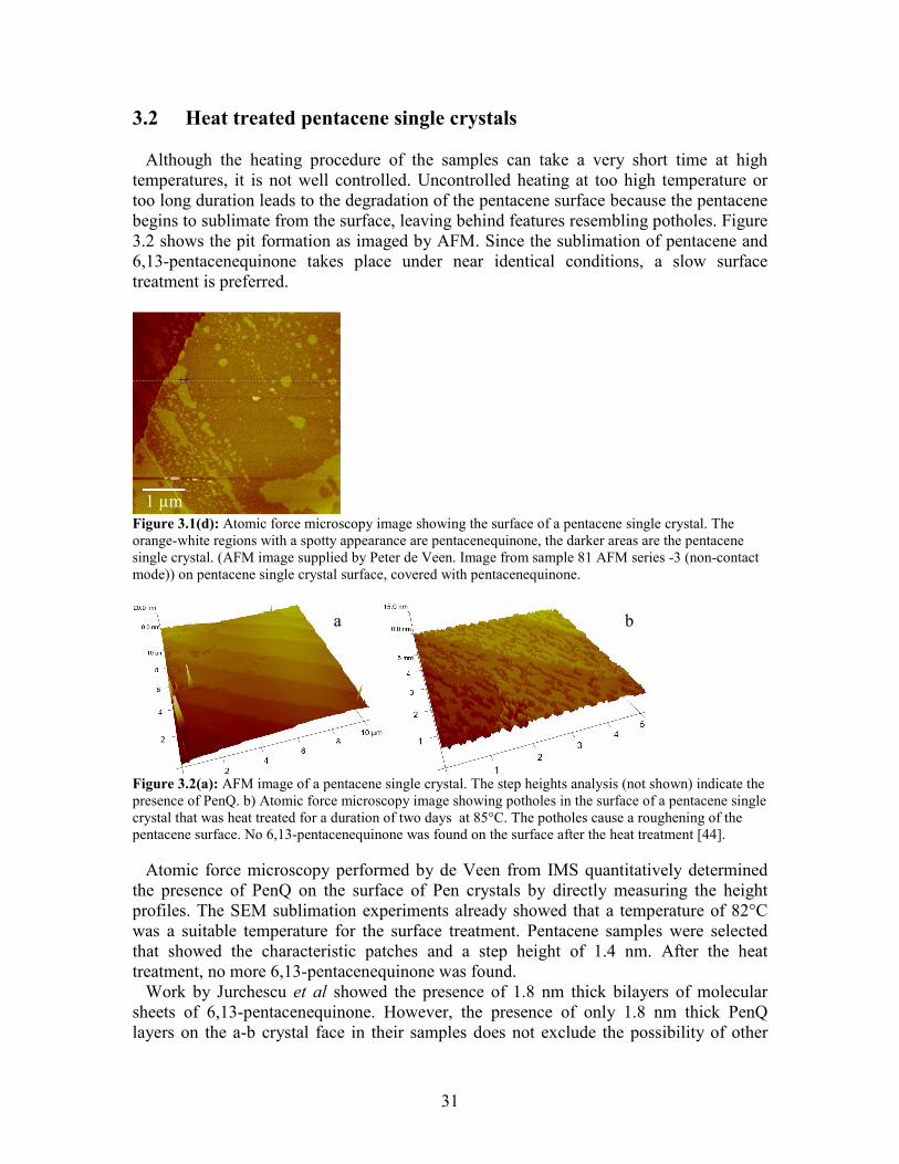
Figure 3.1(d): Atomic force microscopy image showing the surface of a pentacene single crystal. The
orange-white regions with a spotty appearance are pentacenequinone, the darker areas are the pentacene
single crystal. (AFM image supplied by Peter de Veen. Image from sample 81 AFM series -3 (non-contact
mode)) on pentacene single crystal surface, covered with pentacenequinone.
Figure 3.2(a): AFM image of a pentacene single crystal. The step heights analysis (not shown) indicate the
presence of PenQ. b) Atomic force microscopy image showing potholes in the surface of a pentacene single
crystal that was heat treated for a duration of two days at 85°C. The potholes cause a roughening of the
pentacene surface. No 6,13-pentacenequinone was found on the surface after the heat treatment [44].
Atomic force microscopy performed by de Veen from IMS quantitatively determined
the presence of PenQ on the surface of Pen crystals by directly measuring the height
profiles. The SEM sublimation experiments already showed that a temperature of 82°C
was a suitable temperature for the surface treatment. Pentacene samples were selected
that showed the characteristic patches and a step height of 1.4 nm. After the heat
treatment, no more 6,13-pentacenequinone was found.
Work by Jurchescu et al showed the presence of 1.8 nm thick bilayers of molecular
sheets of 6,13-pentacenequinone. However, the presence of only 1.8 nm thick PenQ
layers on the a-b crystal face in their samples does not exclude the possibility of other
1 µm
a b

32
molecular step heights. When the surface was investigated more closely, the step heights
found by AFM, indicated the presence of other combinations of molecular stacking: e.g.
Pen-Pen, Pen-PenQ. Atomic force microscopy cannot show the presence of a full
monolayer coverage of PenQ of the pentacene surface because the step height will be
identical, just translated in the c direction. AFM phase imaging can help to differentiate
these difficult to interpret regions.
Although the preferred crystal growth direction is in the a-b plane, not all of the
received crystals showed large flat a-b terraces. Smooth and large a-b terraces visible
under the optical microscope were a good first indicator for high quality crystals, as
characterized by scanning electron microscopy or AFM.
3.3 In situ heat treated pentacene single crystals
3.3.1 SEM image analysis
In order to get better insight into the processes that govern the selective sublimation of
the surface PenQ, a sequence of SEM images was taken. The image sequence showed the
progress of disappearing surface features while the samples were heated to five different
temperatures (82°C,88°C,91°C,100°C,118°C).
Figure 3.3: Illustration of the SEM imaging process. The front image is taken at time t, while the back
image is taken at time t0.
The samples were heated inside the electron microscope vacuum chamber by a heater
of custom design. During the SEM imaging analysis, monolayers of 6,13-
pentacenequinone were assumed. Low contrast images were semi-automatically
processed by the Image-Magick software and the Perl scripting language.
The number of black, blue, yellow and white pixels were counted by a Perl script. Each
yellow pixel (sample IV) represents a surface area of 6,13-pentacene of 5.7·10-13
m2.
Under the assumption that the surface is covered by a monolayer 6,13-pentacenequinone,
one yellow pixel corresponds to 7.21·10-16
mg PenQ, or 1.41·106 PenQ molecules. The
time

33
details of the calculation can be found in the spreadsheet in the appendix. Plotting the
quantity of surface 6,13-pentacenequinone (normalized to 1 m2) over time yields a
sublimation rate, by fitting a line to the data and taking the derivative.
The present work confirms that 6,13-pentacenequinone is present on the surface of the
as-grown pentacene single crystals, preventing a good ohmic contacts between pentacene
and metal (Au) electrodes. AFM data indicates the presence of monolayers of PenQ.
Although not excluding multilayers of PenQ, this result indicates pentacene can be
oxidized by oxygen from air combined with light when the crystals are stored in a
nitrogen flushed cupboard.
Scanning electron microscopy at low electron beam energy combined with digital
image processing was used to calculate the sublimation rate and energy of PenQ from the
Pen surface. The image processing was done with the open-source software
ImageMagick 6.4.8, controlled by a Perl script (ActivePerl 5.10.0).
3.3.2 Sublimation model 6,13 pentacenequinone
Sublimation is the solid-gas phase transition of a molecular compound. The
Sublimation of 6,13-pentacenequinone from the samples surface takes place, rather than
the evaporation, at the low partial pressure of 6,13-pentacenequinone in the vacuum
while the sample is heated up.
Sublimation of molecular vd Waals compounds was modeled by the empirical
Arrhenius equation 3.1 and plot (Fig. 3.4). The sublimation activation energy can be
found by taking the slope from the data in the Arrhenius plot. The sublimation activation
energy of pentacene and 6,13-pentacenequinone was reported in literature [62]
. However,
to the best knowledge of the author, no activation energy has been published on the
sublimation process of a molecular layer of 6,13-pentacene from the surface of pentacene
single crystals.
R = R0e-Esub/kbT
Eq 3.1
R sublimation rate
R0 sublimation rate at T=∞°C
Esub sublimation activation energy [eV]
kb Boltzmann constant [eVK-1
]
Figure 3.3 shows the decreasing amount of 6,13-pentacenequinone of a sample heated
to 100 °C (See also Fig.2.4). The data of the other temperatures can be found in table 2.1.
From each imaging sequence, the sublimation rate was calculated by this method. These
natural logarithms of the sublimation rates were then plotted as a function of 1/T, to give
the Arhhenius plot. The sublimation energy is calculated from the Arrhenius plot by
taking the derivative, followed by rearranging Eq. 3.1, to give an sublimation activation
energy of 0.85 eV. The intersection of the extrapolated linear fit to the Arrhenius data
give a setpoint R0 of the sublimation rate. The setpoint R0 is directly proportionally to the
assumed thickness of the sublimating layer.

34
As was already observed in the preliminary sublimation experiments, the sublimation
temperature of the surface PenQ is lower than the reported literature values of bulk PenQ.
The sublimation activation energy was calculated by quantitative image analysis of the
SEM image sequences. The Arrhenius plot of the sublimation rates versus the inverse of
the temperature showed an activation energy of 0.85 eV, significant lower than literature
bulk value of 1.2 eV.
However, practical issues of the SEM sublimation rate monitoring experiments limit
the accuracy of the obtained activation energy and more accurate measurement by other
means than SEM are necessary to confirm the results.
Although calculation of R0 is of interest, the sublimation activation energy is the more
interesting physical property in the application of surface cleaning. Fortunately, the
assumption on the PenQ thickness does not effect the calculation of the actrivation
energy; it only translates the linear fit of the Arrhenius plot in the y direction, keeping the
derivative identical.
Figure 3.4 shows an Arrhenius plot using the data in table 2.1. The offset in sublimation
rate-constant was determined by extrapolation of the linear fit in the plot to the
intersection of the y-axis. The activation energy of the sublimation process was
determined by taking the derivative of the linear fit and using the Arrhenius equation.
Figure 3.4: Arrhenius plot of the surface sublimation process. It is assumed that the surface layer consists
of a mono layer of 6,13-pentacenequinone. The thickness of the assumed layer does only affect the R0
(offset) of the sublimation rate; the plot then translates in the y direction. The slope is not a function of the
assumed layer thickness, and consequently, the calculated sublimation activation energy of the process does
not depend of the layer thickness.
35
3.4 Discussion
The principal aim is the fabrication and characterization of single crystal pentacene
field effect transistors (FET). The fabrication of field effect devices provides a viable way
of getting information about the intrinsic properties of pentacene. The realization of the
FET devices require suitable fabrication techniques. The FETs also require good starting
materials in the form of well grown pentacene single crystals. In literature Pen powders
are purified by a sublimation method. An analysis of the surface using sequences of SEM
images resulted in a cleaning procedure and an estimation of the sublimation activation
energy.
The activation energy that was determined from the SEM image analysis is lower than
the (similar system) sublimation energy of pure PenQ, although not more then a factor of
two. The exact cause is uncertain at this point because it was experimentally challenging
to get suitable data from the experiments. More data points would help, but as
mentioned, getting more data for the SEM image analysis is impractical. But qualitative,
it is clear that the sublimation process proceeds more facile than the sublimation of pure
PenQ as evidenced by the lower temperature needed and the high sublimation rate found
of the surface layer.
3.5 Recommendations
It is recommended to setup an experiment that will monitor the surface of pentacene
crystals as a function of the temperature with an AFM system.
It would be interesting to not only fabricate FETs on the single crystal surface and
characterize them, but do a comparison of the performance of devices fabricated on the
surface with untreated crystals and fabricate identical devices using the cleaned devices.
Improvements are expected in a lowered contact resistance, but also in an increased
mobility in the channel.
An interesting experiment would entail testing the energetic-disorder-sensitivity of the
field effect mobility of devices fabricated on a-b planes compared to devices fabricated
on the a-c/b-c planes. It is expected that the field effect mobilities of the devices
fabricated on the a-c/b-c plane are slightly smaller than the a-b devices (both using highly
purified single crystals). However, it is hypothized that the a-c FET devices will perform
better with increased defect concentration. The applied electric field from the gate forces
the charge carriers against the pentacene/insulator interface. But since the a-b planes now
are parallel with the a-c plane exposed, charge carriers have more freedom of movement
when facing an energy bump or hill. The carriers do not need to jump from and to
different a-b molecular sheets.
36
4 Conclusions
The relevant literature on the organic semiconductor pentacene was reviewed.
Pentacene has become an important model system for the fundamental studies on organic
semiconductors. An introduction to organic semiconductor theory was presented (Ch. 1).
A cleaning procedure of the pentacene single crystals was proposed, based on the
difference in sublimation behavior of the two main components, pentacene and 6,13-
pentacenequinone (Ch. 2).
The surface of pentacene single crystals was characterized by SEM, at a low electron
beam acceleration voltage (0.3 kV and 0.5 kV). (Ch. 3). The low electron beam energy
insured that only the surface of the crystals was imaged. It was shown by SEM and
AFM[44]
that patches of varying thickness and area size were present on the as-received
physical-vapor-grown pentacene single crystals. It was found that 6,13-pentacenequinone
(PenQ) is present on the surface of these crystals, indicated by the molecular step heights
measured by AFM.
The proposed cleaning method was successfully applied in removing the surface layer
PenQ. The PenQ surface layer could be removed by heat-treating the pentacene single
crystals samples in a vacuum, although the temperature range was found to be narrow.
An semi-automatic SEM image processing technique was developed to monitor the
surface sublimation process more accurately. The sublimation rate was 75 nmol·h-1
·m-2
and 1933 nmol·h-1
·m-2
at 82°C and 118°C respectively. The samples were imaged by SEM
while they were being heated inside the vacuum chamber of the SEM. An SEM sample
heater was developed for the experiment. The sublimation activation energy of the
cleaning process was determined (0.85 eV) using the same imaging data. A standardized
cleaning procedure was recommended from these results.
37
Acknowledgements
The help of many people is greatly acknowledged, without which the present work
would have been so much harder to do. Understandable, I cannot list everybody because
then the list would get too long. So, to all the people I have forgotten to include in this
list; my sincerest apologies. Having said that, I first would like to thank Yvo Brevoort
who helped me forming a strategy for the SEM image analysis and programmed the Perl
image process automation script. I would to express my gratitude to Peter de Veen, for
his good mentoring and guiding me in finding my ways in the academic world. Next, I
thank Guus Rijnders for his guidance and pointing me to an interesting master thesis
project subject. I thank Wilfred van der Wiel for being in my Graduation Committee. Of
cource, my thanks goes to David Blank for his cooking skills and playing a good host. I
thank my parent, Jannette Martine van Vlaanderen and Eduard van Bemmel for their
support and for believing in me. Then I would like to thank Kicki Martens, for perhaps
unknowingly, motivating me to go forwards during difficult times. And lastly, and
perhaps most importantly, I am thanking my sweet girlfriend Anke Koopmans. I cannot
put into words how much I am grateful for all her support, and sometimes putting up with
me, over the last few years. Anke, this work is dedicated to you.
Gerard.

38
References
[1] http://www.pbs.org/transistor/science/events/silicont1.html
[2] Gelinck, G. H., H. E. A. Huitema, et al. (2004). "Flexible active-matrix displays
and shift registers based on solution-processed organic transistors." Nature
Materials 3(2): 106-110.
[3] Parisse, P., S. Picozzi, et al. (2007). "Electronic, morphological and transport
properties of 6,13-pentacenequinone thin films: Theory and experiments."
Organic Electronics 8(5): 498-504.
[4] Jurchescu, O. D., J. Baas, et al. (2005). "Electronic transport properties of
pentacene single crystals upon exposure to air." Applied Physics Letters 87(5).
[5] Reese, C. and Z. N. Bao (2006). "Organic single crystals: tools for the exploration
of charge transport phenomena in organic materials." Journal of Materials
Chemistry 16(4): 329-333.
[6] Koch, N. (2008). "Energy levels at interfaces between metals and conjugated
organic molecules." Journal of Physics-Condensed Matter 20(18).
[7] Chapman, B. D., A. Checco, et al. (2006). "Dislocations and grain boundaries in
semiconducting rubrene single-crystals." Journal of Crystal Growth 290(2): 479-
484.
[8] Alves, H., A. S. Molinari, et al. (2008). "Metallic conduction at organic charge-
transfer interfaces." Nature Materials 7(7): 574-580.
[9] Reese, C. and Z. N. Bao (2007). "Organic single-crystal field-effect transistors."
Materials Today 10(3): 20-27.
[10] Mori, T. (2008). "Molecular materials for organic field-effect transistors." Journal
of Physics-Condensed Matter 20(18).
[11] Horowitz, G. (2004). "Organic thin film transistors: From theory to real devices."
Journal of Materials Research 19(7): 1946-1962.
[12] Kitamura, M. and Y. Arakawa (2008). "Pentacene-based organic field-effect
transistors." Journal of Physics: Condensed Matter 20(18): 184011.
[13] Dimitrakopoulos, C. D. and D. J. Mascaro (2001). "Organic thin-film transistors:
A review of recent advances." Ibm Journal of Research and Development 45(1):
11-27.
[14] Molinari, A., I. Gutierrez, et al. (2007). "Bias-dependent contact resistance in
rubrene single-crystal field-effect transistors." Applied Physics Letters 90(21).
[15] Jurchescu, O. D., M. Popinciuc, et al. (2007). "Interface-controlled, high-mobility
organic transistors." Advanced Materials 19(5): 688-+.
[16] Noh, Y. Y., N. Zhao, et al. (2007). "Downscaling of self-aligned, all-printed
polymer thin-film transistors." Nature Nanotechnology 2(12): 784-789.
[17] Kim, D. and J. Moon (2005). "Highly conductive ink jet printed films of
nanosilver particles for printable electronics." Electrochemical and Solid State
Letters 8(11): J30-J33.
[18] Xue, F. L., Z. C. Liu, et al. (2006). "Inkjet printed silver source/drain electrodes
for low-cost polymer thin film transistors." Microelectronic Engineering 83(2):
298-302
39
[19] Plotner, M., T. Wegener, et al. (2004). "Investigation of ink-jet printing of poly-3-
octylthiophene for organic field-effect transistors from different solutions."
Synthetic Metals 147(1-3): 299-303.
[20] Liu, Y., K. Varahramyan, et al. (2005). "Low-voltage all-polymer field-effect
transistor fabricated using an inkjet printing technique." Macromolecular Rapid
Communications 26(24): 1955-1959.
[21] Chang, P. C., S. E. Molesa, et al. (2006). "Inkjetted crystalline single monolayer
oligothiophene OTFTs." Ieee Transactions on Electron Devices 53(4): 594-600.
[22] Song, D. H., M. H. Choi, et al. (2007). "Process optimization of organic thin-film
transistor by ink-jet printing of DH4T on plastic." Applied Physics Letters 90(5).
[23] Chiang, C. K., M. A. Druy, et al. (1978). "Synthesis of Highly Conducting Films
of Derivatives of Polyacetylene, (Ch)X." Journal of the American Chemical
Society 100(3): 1013-1015.
[24] Hadziioannou G., Hutten P.F. van. “Semiconducting Polymers: Chemistry,
Physics and Engineering.” Wiley-VCH Verlag GmbH, 2000.
[25] Mostovoy, M. V., M. T. Figge, et al. (1997). "Disorder-induced solitons in
conjugated polymers." Europhysics Letters 38(9): 687-692.
[26] Reese, C. and Z. N. Bao (2007). "Organic single-crystal field-effect transistors."
Materials Today 10(3): 20-27.
[27] Perez-Garcia, B., J. Abad, et al. (2008). "Surface potential domains on lamellar
P3OT structures." Nanotechnology 19(6).
[28] Muck, T., V. Wagner, et al. (2004). "In situ electrical characterization of DH4T
field-effect transistors." Synthetic Metals 146(3): 317-320.
[31] Al-Mahboob, A., J. T. Sadowski, et al. (2008). "Kinetics-driven anisotropic
growth of pentacene thin films." Physical Review B 77(3).
[32] Beernink, G., T. Strunskus, et al. (2004). "Importance of dewetting in organic
molecular-beam deposition: Pentacene on gold." Applied Physics Letters 85(3):
398-400.
[33] Wu, Y., T. Toccoli, et al. (2007). "Controlling the early stages of pentacene
growth by supersonic molecular beam deposition." Physical Review Letters 98(7).
[34] Goose, J. E. and P. Clancy (2007). "Exploring the energetic deposition of
pentacene on pentacene through molecular dynamics Simulations." Journal of
Physical Chemistry C 111(43): 15653-15659.
[35] Yanagisawa, H., T. Tamaki, et al. (2004). "Structural and electrical
characterization of pentacene films on SiO2 grown by molecular beam
deposition." Thin Solid Films 464-65: 398-402.
[36] Yaginuma, S., K. Itaka, et al. (2008). "Composition-spread thin films of
pentacene and 6,13-pentacenequinone fabricated by using continuous-wave laser
molecular beam epitaxy." Applied Surface Science 254(8): 2336-2341.
[37] Itaka, K., T. Hayakawa, et al. (2004). "Pulsed laser deposition of c(*) axis
oriented pentacene films." Applied Physics a-Materials Science & Processing
79(4-6): 875-877.
[38] Blanchet, G. B., C. R. Fincher, et al. (2003). "Laser evaporation and the
production of pentacene films." Journal of Applied Physics 94(9): 6181-6184.
40
[39] Maud, J. M., A. J. Salih, et al. (1999). "Enhanced field effect carrier mobilities in
pentacene based thin film transistors via pulsed laser deposition." Synthetic
Metals 102(1-3): 986-986.
[40] Salih, A. J., S. P. Lau, et al. (1996). "Improved thin films of pentacene via pulsed
laser deposition at elevated substrate temperatures." Applied Physics Letters
69(15): 2231-2233.
[41] Yamaguchi, J., K. Itaka, et al. (2004). "Combinatorial pulsed laser deposition of
pentacene films for field effect devices." Macromolecular Rapid Communications
25(1): 334-338.
[43] Inorganic Material Science group, University of Twente.
[44] P. de Veen (2008). Unpublished work.
[45] Jurchescu, O. D., J. Baas, et al. (2004). "Effect of impurities on the mobility of
single crystal pentacene." Applied Physics Letters 84(16): 3061-3063.
[46] Jurchescu, O. D., M. Popinciuc, et al. (2007). "Interface-controlled, high-mobility
organic transistors." Advanced Materials 19(5): 688-+.
[47] Marc M Faktor, Ian Garret (1974). “Growth of crystals from the vapour”.
Chapman and Hall, London. ISBN 0412113201.
[48] Calhoun, M.F., et al. (2007). “Electronic functionalization of the surface of
organic semiconductors with self-assembled monolayers.”
[49] Yasuda, T., Goto, T., Fujita, K., Tsutsui, T. (2004). “Ambipolar pentacene field-
effect transistors with calcium source-drain electrodes.” Applied Physics Letters.
85(11):2089.
[50] Yagi, I., K. Tsukagoshi, et al. (2004). "Direct observation of contact and channel
resistance in pentacene four-terminal thin-film transistor patterned by laser
ablation method." Applied Physics Letters 84(5): 813-815.
[51] Yang, H. C., L. Yang, et al. (2008). "Aging Susceptibility of Terrace-Like
Pentacene Films." Journal of Physical Chemistry C 112(42): 16161-16165.
[52] Yaginuma, S. et al. (2007). “Continuous wave infrared laser deposition of organic
thin films.” Journal of Physics 59(2007).
[53] Masif pulsed laser system IMS group utwente.
[54] Vollmer, A., O. D. Jurchescu, et al. (2005). "The effect of oxygen exposure on
pentacene electronic structure." European Physical Journal E 17(3): 339-343.
[55] Conrad, B. R., E. Gomar-Nadal, et al. (2008). "Effect of impurities on
pentacene island nucleation." Physical Review B 77(20): 5.
[56] De Angelis, F., M. Gaspari, et al. (2009). "Direct mass spectrometry investigation
on Pentacene thin film oxidation upon exposure to air." Chemical Physics Letters
468(4-6): 193-196.
[57] Northrop, B. H., J. E. Norton, et al. (2007). "On the mechanism of peripentacene
formation from pentacene: Computational studies of a prototype for graphene
formation from smaller acenes." Journal of the American Chemical Society
129(20): 6536-6546.
[58] Parisse, P., S. Picozzi, et al. (2007). "Electronic, morphological and transport
properties of 6,13-pentacenequinone thin films: Theory and experiments."
Organic Electronics 8(5): 498-504.
41
[59] Koch, N., I. Salzmann, et al. (2006). "Molecular orientation dependent energy
levels at interfaces with pentacene and pentacenequinone." Organic Electronics
7(6): 537-545.
[60] Image Magick 6.4.8.Q16. Available online at http://www.imagemagick.org.
[61] ActivePerl 5.10.0. Available online at http://www.perl.com.
[62] Kafer, D., M. El Helou, et al. (2008). "Packing of planar organic molecules:
Interplay of van der waals and electrostatic interaction." Crystal Growth & Design
8(8): 3053-3057.
[63] Goldmann, C., D. J. Gundlach, et al. (2006). "Evidence of water-related discrete
trap state formation in pentacene single-crystal field-effect transistors." Applied
Physics Letters 88(6).
[64] Qiu, Y., Y. C. Hu, et al. (2003). "H2O effect on the stability of organic thin-film
field-effect transistors." Applied Physics Letters 83(8): 1644-1646.
[65] Goldmann, C., D. J. Gundlach, et al. (2006). "Evidence of water-related discrete
trap state formation in pentacene single-crystal field-effect transistors." Applied
Physics Letters 88(6).
[66] Laudise, R. A., C. Kloc, et al. (1998). "Physical vapor growth of organic
semiconductors." Journal of Crystal Growth 187(3-4): 449-454.
[67] Reese, C. and Z. N. Bao (2007). "Organic single-crystal field-effect transistors."
Materials Today 10(3): 20-27.
[68] AGA gas company is now part of the Linde gas group. http://www.lindegas.com
[69] C. D. Dimitrakopoulos, D. J. Mascaro (2001). “Organic thin film transistors:
A review of recent advances.” IBM J. Res. Dev. 45(1):11-27.
[70] Wu, Y., T. Toccoli, et al. (2007). "Controlling the early stages of pentacene
growth by supersonic molecular beam deposition." Physical Review Letters 98(7).
[71] Jurchescu, O. D., B. H. Hamadani, et al. (2008). "Correlation between
microstructure, electronic properties and flicker noise in organic thin film
transistors." Applied Physics Letters 92(13).
[72] Tesconi, M., M. J. Pikal, et al. (1997). "A method for the rapid estimation of
sublimation rates of organic compounds at standard temperature and pressure."
Journal of Pharmaceutical Sciences 86(11): 1299-1302.
[73] Weng, S. Z., W. S. Hu, et al. (2006). "Anisotropic field-effect mobility of
pentacene thin-film transistor: Effect of rubbed self-assembled monolayer."
Applied Physics Letters 89(17).
[74] Hwang, D. K., K. Kim, et al. (2005). "Structural and optical properties of 6,13-
pentacenequinone film." Applied Surface Science 244(1-4): 615-618.
[75] Vollmer, A., H. Weiss, et al. (2006). The interaction of oxygen and ozone with
pentacene.
[76] Salzmann, I., R. Opitz, et al. (2007). "Phase separation in vacuum codeposited
pentacene/6,13-pentacenequinone thin films." Physical Review B 75(17).
[77] Takenobu, T., K. Watanabe, et al. (2008). "Effect of postannealing on the
performance of pentacene single-crystal ambipolar transistors." Applied Physics
Letters 93(7).
[78] De Angelis, F., M. Gaspari, et al. (2009). "Direct mass spectrometry investigation
on Pentacene thin film oxidation upon exposure to air." Chemical Physics Letters
468(4-6): 193-196.

42
[79] http://www.highbeam.com/doc/1P3-1467974631.html
[80] Dzyabchenko, A. V., V. E. Zavodnik, et al. (1979). "6,13-Pentacenequinone -
Molecular Packing Analysis." Acta Crystallographica Section B-Structural
Science 35(SEP): 2250-2253.
[81] http://nl.wikipedia.org/wiki/John_Maynard_Keynes
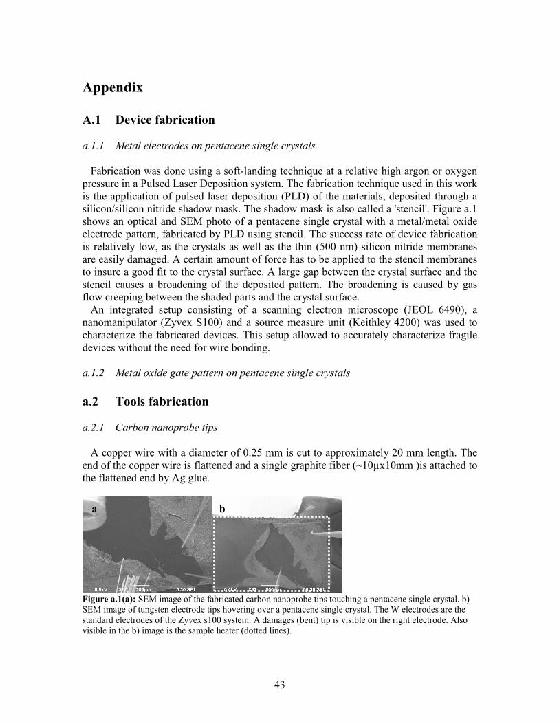
43
Appendix
A.1 Device fabrication
a.1.1 Metal electrodes on pentacene single crystals
Fabrication was done using a soft-landing technique at a relative high argon or oxygen
pressure in a Pulsed Laser Deposition system. The fabrication technique used in this work
is the application of pulsed laser deposition (PLD) of the materials, deposited through a
silicon/silicon nitride shadow mask. The shadow mask is also called a 'stencil'. Figure a.1
shows an optical and SEM photo of a pentacene single crystal with a metal/metal oxide
electrode pattern, fabricated by PLD using stencil. The success rate of device fabrication
is relatively low, as the crystals as well as the thin (500 nm) silicon nitride membranes
are easily damaged. A certain amount of force has to be applied to the stencil membranes
to insure a good fit to the crystal surface. A large gap between the crystal surface and the
stencil causes a broadening of the deposited pattern. The broadening is caused by gas
flow creeping between the shaded parts and the crystal surface.
An integrated setup consisting of a scanning electron microscope (JEOL 6490), a
nanomanipulator (Zyvex S100) and a source measure unit (Keithley 4200) was used to
characterize the fabricated devices. This setup allowed to accurately characterize fragile
devices without the need for wire bonding.
a.1.2 Metal oxide gate pattern on pentacene single crystals
a.2 Tools fabrication
a.2.1 Carbon nanoprobe tips
A copper wire with a diameter of 0.25 mm is cut to approximately 20 mm length. The
end of the copper wire is flattened and a single graphite fiber (~10µx10mm )is attached to
the flattened end by Ag glue.
Figure a.1(a): SEM image of the fabricated carbon nanoprobe tips touching a pentacene single crystal. b)
SEM image of tungsten electrode tips hovering over a pentacene single crystal. The W electrodes are the
standard electrodes of the Zyvex s100 system. A damages (bent) tip is visible on the right electrode. Also
visible in the b) image is the sample heater (dotted lines).
a b
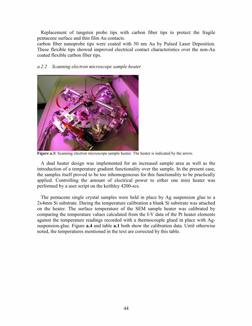
44
Replacement of tungsten probe tips with carbon fiber tips to protect the fragile
pentacene surface and thin film Au contacts.
carbon fiber nanoprobe tips were coated with 50 nm Au by Pulsed Laser Deposition.
These flexible tips showed improved electrical contact characteristics over the non-Au
coated flexible carbon fiber tips.
a.2.2 Scanning electron microscope sample heater
Figure a.3: Scanning electron microscope sample heater. The heater is indicated by the arrow.
A dual heater design was implemented for an increased sample area as well as the
introduction of a temperature gradient functionality over the sample. In the present case,
the samples itself proved to be too inhomogeneous for this functionality to be practically
applied. Controlling the amount of electrical power to either one mini heater was
performed by a user script on the keithley 4200-scs.
The pentacene single crystal samples were held in place by Ag suspension glue to a
2x4mm Si substrate. During the temperature calibration a blank Si substrate was attached
on the heater. The surface temperature of the SEM sample heater was calibrated by
comparing the temperature values calculated from the I-V data of the Pt heater elements
against the temperature readings recorded with a thermocouple glued in place with Ag-
suspension-glue. Figure a.4 and table a.1 both show the calibration data. Until otherwise
noted, the temperatures mentioned in the text are corrected by this table.

45
Figure a.4: Calibration curve of the scanning electron microscope sample heater, based on the HA 421
platinum temperature sensors, kindly provided by Joska Broekmaat. X-axis denote the temperature as
calculated from the I-V heater element data. Y-axis show the surface temperature on the silicone substrate
measured by a thermocouple.
Table a.1: Calibration curve data showing the difference in calculated and measured temperature in the
third column.
Sample heater [ºC] Thermocouple [ºC] ∆T [ºC] 68 57 11 81 69 12 111 97 14 132 117 15
Note: The linear fit equation is Theater = 0.9372·Tthermocouple – 6.8409
a.2.3 Flexible polymer masks
The broadening of the patterns can prevented by using a polymer foil based stencil
instead of the silicon nitride stencil. The suitability of the polymer stencils is based on the
elasticity and plasticity of polymers. The foils prevent damage to the fragile pentacene
surface. The pattern was fabricated into the polymer foils (Kaptop™) by using pulsed
laser ablation. These same flexible stencils formed the bases to prototype of an automized
mask positioned, for use in the vacuum chamber of the pulsed laser system. The mask
positioner can save time and exclude the influence of the ambient atmosphere when the
samples are taken out of the system during stencil change. Multiple aligned patterns are
necessary for the fabrication of a field effect transistor on the surface of the crystals.
The mask patterns were ablated into (6-8) micron thick polyimide films by using a
stainless steel YAG-laser cut mask template of larger dimensions, and positioning its
image onto the polyimide foils. Polyimide foils was selected as it has (i) a high melting
point, allowing patterning at the micrometer scale and (ii) has a high absorbance for
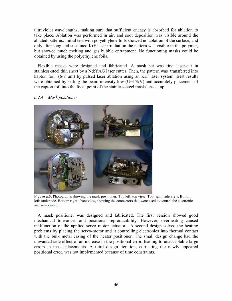
46
ultraviolet wavelengths, making sure that sufficient energy is absorbed for ablation to
take place. Ablation was performed in air, and soot deposition was visible around the
ablated patterns. Initial test with polyethylene foils showed no ablation of the surface, and
only after long and sustained KrF laser irradiation the pattern was visible in the polymer,
but showed much melting and gas bubble entrapment. No functioning masks could be
obtained by using the polyethylene foils.
Flexible masks were designed and fabricated. A mask set was first laser-cut in
stainless-steel thin sheet by a Nd:YAG laser cutter. Then, the pattern was transferred into
kapton foil (6-8 µm) by pulsed laser ablation using an KrF laser system. Best results
were obtained by setting the beam intensity low (U~17kV) and accurately placement of
the capton foil into the focal point of the stainless-steel mask/lens setup.
a.2.4 Mask positioner
Figure a.5: Photographs showing the mask positioner. Top left: top view. Top right: side view. Bottom
left: underside. Bottom right: front view, showing the connectors that were used to control the electronics
and servo motor.
A mask positioner was designed and fabricated. The first version showed good
mechanical tolerances and positional reproducibility. However, overheating caused
malfunction of the applied servo motor actuator. A second design solved the heating
problems by placing the servo-motor and it controlling electronics into thermal contact
with the bulk metal casing of the heater positioner. The small design change had the
unwanted side effect of an increase in the positional error, leading to unacceptable large
errors in mask placements. A third design iteration, correcting the newly appeared
positional error, was not implemented because of time constraints.
47
In situ device fabrication with the mask positioner
The design goal was to have the mask positioner functionality without having to modify
the electrical connector on the Masif PLD system, and thereby making the mask
positioner compatible with any of the PLD systems that make use of the standardized 3-
pin connectors. Electrical connection backwards compatible with the existing mechanical
connectors. Preventing (re)oxidation of the pentacene surface, and increasing the
workflow efficiency. Preparation is in progress to do all the necessary patterning steps in
situ by using a new mask positioning system.
A new flexible mask positioning technique was developed to prevent damage to the
fragile pentacene single crystals, as well as substantially decrease the gap between the
mask and substrate normally encountered when using conventional Si/SiNx or metal
masks. It was noted that the crystals had tendency to break, particularly in the a-b
direction. The fragile pentacene crystals motivated the development of novel ways in
crystal handling and device fabrication.
a.3 SEM image processing
a.3.1 Perl script
The Perl script reads the input SEM images from the /input/ folder and puts the
processed images under /output/. In the same output folder, the Perl script creates a .csv
file containing the individual file names, pixel count and time stamps
Filename: Convert.pl use strict; use Image::Magick; # Image manipulatie lib use Win32::FileTime; # Lib voor het uitlezen van informatie over
tijden die opgeslagen zijn in een bestand (creation, modify etc). # Directory namen voor input en output. Alle files in input worden als
bronbestand opgepikt, geconverteerd en daarna in de output dir weggeschreven na bewerking. # Deze mappen moeten bestaan, anders werkt het niet! my $inputdir = "input"; my $outputdir = "output"; # En dit bepaald dan hoe groot het gebied moet worden. Als je het hele
plaatje wilt hebben zet je deze op de afmetingen van de plaatjes (2560 en 1920). my $crop_x_size = 474; my $crop_y_size = 275; # Crop X start, Crop Y start is vanaf waar in het plaatje je wilt
knippen. Als je het hele plaatje zou willen hebben zet je deze op 0, 0 my $crop_x_start = 210; my $crop_y_start = 100;

48
# Haal een lijst op van de bestanden uit de input directory. my @files = ( ); opendir ( DIR, $inputdir ) || die "Error in opening dir $inputdir\n"; while (my $filename = readdir(DIR)){ push @files, $filename; } closedir(DIR); # Open het CSV bestand waar we de uitgelezen waardes in gaan opslaan,
en schrijf de koppen definitie er in. open CSV, "> " . $outputdir . "/fileinfo.csv"; print CSV
'"filename";"blacks";"blues";"yellows";"whites";"modifyyear";"modifymonth";"modifyday";"modifyhour";"modifyminute";"modifysecond"' . "\n"; # Loop over alle inputbestanden heen, en doe je ding. foreach my $file (@files) { my $filename = $inputdir . '/' . $file; print "Processing $filename\n"; # We slaan directories over, en gaan alleen aan de slag met
bestanden uit de input map. if (-d $filename) { next; } # Maak het image magick object aan, en lees het invoerbestand my $image = Image::Magick->new; $image->Read($filename); # Lees de tijdinformatie uit het bestand. my $filetime = Win32::FileTime->new( $filename ); my @modify = $filetime->Modify( 'year', 'month', 'day', 'hour', 'minute', 'second' ); # Image Magick bewerkingen om het plaatje om te vorm en meetbaar
te maken. $image->Blur(radius => 10, sigma => 2); #$image->Contrast(sharpen => 0); $image->Contrast(sharpen => 0); $image->Quantize(colorspace => 'Gray', colors => 4, dither => 0); $image->Crop(geometry=>$crop_x_size . 'x' . $crop_y_size . '+' .
$crop_x_start . '+' . $crop_y_start); # Haal histogram informatie van de afbeelding. Bepaal aan de hand
van de waardes de huidige kleurwaardes die we willen converteren naar zwart, blauw, geel en wit. my @histogram = $image->Histogram();
49
my $black = "#" . sprintf("%4x", $histogram[0]) . sprintf("%4x", $histogram[1]) . sprintf("%4x", $histogram[2]) . sprintf("%4x", $histogram[3]); my $blue = "#" . sprintf("%4x", $histogram[5]) .
sprintf("%4x", $histogram[6]) . sprintf("%4x", $histogram[7]) . sprintf("%4x", $histogram[8]); my $yellow = "#" . sprintf("%4x", $histogram[10]) .
sprintf("%4x", $histogram[11]) . sprintf("%4x", $histogram[12]) . sprintf("%4x", $histogram[13]); my $white = "#" . sprintf("%4x", $histogram[15]) .
sprintf("%4x", $histogram[16]) . sprintf("%4x", $histogram[17]) . sprintf("%4x", $histogram[18]); # Converteer de grijstinten naar zwart, blauw, geel en wit. $image->Opaque(color => $black, fill => "black"); $image->Opaque(color => $blue, fill => "blue"); $image->Opaque(color => $yellow, fill=> "yellow"); $image->Opaque(color => $white, fill=> "white"); # Schrijf het geconverteerde bestand weg naar de output
directory. Deze krijgt dezelfde naam die het inputbestand heeft voor latere referentie. $image->Write(filename => $outputdir . "/" . $file); # Schrijf de informatie over deze afbeelding naar de CSV. print CSV '"' . $file . '";'; # filename print CSV '"' . $histogram[4] . '";'; # blacks print CSV '"' . $histogram[9] . '";'; # blues print CSV '"' . $histogram[14] . '";'; # yellows print CSV '"' . $histogram[19] . '";'; # whites print CSV '"' . $modify[0] . '";'; # modification year print CSV '"' . $modify[1] . '";'; # modification month print CSV '"' . $modify[2] . '";'; # modification day print CSV '"' . $modify[3] . '";'; # modification hour print CSV '"' . $modify[4] . '";'; # modification minutes print CSV '"' . $modify[5] . '"'. "\n"; # modification seconds } # Sluit het CSV bestand en schrijf de gegevens weg.
close CSV;
2419technologies.
2419t_MTGvB_01022009.doc

50