Subjects from the book by Johns & Martin
24
5/25/2010 1 INF4420 Repetition Tuesday 25th of May, 2010, 9:15 Snorre Aunet, [email protected] Nanoelectronics Group, Dept. of Informatics Office 3432 Subjects from the book by Johns & Martin • Chapter 2 Processing and Layout • Chapter 8 Sample and Holds Voltage References and • Chapter 8 Sample and Holds, Voltage References, and Translinear Circuits • Chapter 9 Discrete-Time Signals • Chapter 10 Switched-Capacitor Circuits • Chapter 11 Data Converter Fundamentals • Chapter 12 Nyquist-Rate D/A Converters • Chapter 13 Nyquist-Rate A/D Converters • Chapter 14 Oversampling Converters • Chapter 16 Phase-Locked Loops
Transcript of Subjects from the book by Johns & Martin

5/25/2010
1
INF4420 RepetitionTuesday 25th of May, 2010, 9:15
Snorre Aunet, [email protected] Group, Dept. of Informatics
Office 3432
Subjects from the book by Johns & Martin
• Chapter 2 Processing and Layout• Chapter 8 Sample and Holds Voltage References and• Chapter 8 Sample and Holds, Voltage References, and
Translinear Circuits• Chapter 9 Discrete-Time Signals• Chapter 10 Switched-Capacitor Circuits• Chapter 11 Data Converter Fundamentals• Chapter 12 Nyquist-Rate D/A Converters• Chapter 13 Nyquist-Rate A/D Converters• Chapter 14 Oversampling Converters• Chapter 16 Phase-Locked Loops

5/25/2010
2
Chapter 8 Sample-and-Holds, Voltage References, Translinear Circuits
• Samples an analog signal andstores it for some time
• Often limiting the performancefor Analog-to-Digital Converters
Vin Vout1
clk
Chld
Q1 V
for Analog-to-Digital Converters • Performance limitations: hold step,
feedthrough, bandwidth (sample mode) and slew rate, droop rate, aperture jitter
• Charge injection• We have seen different topologies, having different
Chld
p g ginput impedance, operational speed, susceptibility to clock feedthrough, slewing properties, signal dependent charge injection etc.
Charge injection due to channel capacitance
clkWhen goes low, the channel charge of is equally distributed between source and drain, leaving 50% of the charge across Chld:
Q1
QQCH CoxWLVeff-1
= =
VQC-hld
Chld------------------- CoxWL VDD Vtn Vin––
2Chld----------------------------------------------------------------–= =
Veff-1 VGS1 Vtn– VDD Vtn Vin––= =
QChld 2
-----------2
---------------------------------= =
• is linearly related to Vin, resulting in a gain error for the S/H. There is also a linear relationship to Vtn, which is nonlinearly related to Vin ( through Vsb ) resulting in distortion for the overall S/H.
V

5/25/2010
3
Charge injection due to the gate overlap capacitance:
•
VCox WLov VDD VSS–
Chld--------------------------------------------------------–
• (See eq. 7.8) This component is usually smaller than that due to the channel charge, and appears as an offset, since it’s signal independent.
hld
Thus it may be removed in most systems.• The clock signal should be relatively noise free, as
the power-supply rejection ratio might be poor.
Hold step reduction
Vin Vout1
Chld
Q1 V
clk
clk
Vin Vout1
Chld
Q1 VQ2
clkclkslightly delayed
• Transmission gate reduces charge injection since the charge carriers in the NMOS and PMOS have inversed polarity -> The negative charge from the NMOS cancels the positive charge from the PMOS
• PMOS and NMOS are however hard to match in size, reducing the benefit.
• A NMOS dummy switch (S and D short circuited) of half channel area
CMOS transmission gate Dummy switch
• A NMOS dummy switch (S and D short-circuited) of half channel area clocked on inverted clock may be used to absorb charge
• Hold step reduced by approximately 80%• The dummy switch clock must be slightly delayed to ensure that no charge leaks
through Q1 while it is still open

5/25/2010
4
Bandgap reference - Basic principle
IB
VBE
• The voltage VBE is CTAT• The voltage is PTAT• is scaled by K to get the same slope as VBE
VBEVBE
PTAT Generator K
VBEΔ
V ref VBE K VBEΔ+=
is scaled by K to get the same slope as VBE
• By adding VBE and K , the output Vref
becomes independent of temperatureVBE
VBE
Theory• Collector current
• Solved with respect to VBE:
IC IseV
BEkT q
=
p BE
- The collector current density is related to the current:- The difference between two junctions biased at different
densities: IC AEJC=
VBE VG0 1TT0------–
VBE0
TT0------ mkT
q------------ ln
T0
T------ kT
q------- ln
JC
JC0--------
+ + +=
VBE V2 V1–kTq
------- lnJ2
J1----
= =

5/25/2010
5
Theory• Assuming that:
• Vref can then be written as:
Ji
Ji0------ T
T0------=
Vref can then be written as:
• For a given temperature this equation may be independent of changes in the temperature if a proper
Vref VBE2 K VBE+=
VG0TT0------ VBE0-2 VG0– m 1–
kTq
------- lnT0
T------ K
kTq
------- lnJ2
J1----
+ + +=
vaule of K is assigned
Theory• The change in Vref with respect to the temperature is:
• For zero temperature dependence at the
VrefT
------------ 1T0------ VBE0-2 VG0– K
kq--- ln
J2
J1---- m 1–
kq--- ln
T0
T------ 1–
+ +=
T T0=p pfollowing applies:
• Solving with respect to K gives:
0
VBE0-2 KkT0
q--------- ln
J2
J1----
+ VG0 m 1– kT0
q---------+=
kT
KVG 0 m 1–
kT0
q--------- VB E0-2–+
kT 0
q--------- ln
J2
J1----
--------------------------------------------------------------------1,24 VB E0-2–
0,0258 lnJ2
J1----
---------------------------------= =

5/25/2010
6
Chapter 9 Discrete-Time Signals
• Understanding theory and methods concerning Discrete-Time Signals are important in IC-design:
• The design of Switch-Capacitor filters and their analysis• The design of Switch-Capacitor filters and their analysis are based on discrete-time signal processing
• Discrete-time signal processing are necessary during analysis and design of oversampled data converters (Delta-Sigma) used in for example audio and instrumentation
• Digital filter design is also related to concepts from this g ta te des g s a so e ated to co cepts o t schapter
Overview of signal spectra – conceptual and physical realizations
convert todiscrete-time
sequenceDSP
convert toimpulse
trainhold
analog
low-passfilter
xc t( )
s t( )
xs t( )
x n( ) xc nT( )=y n( ) ys t( ) ysh t( )
yc t( )
• An anti-aliasing filter (not shown) is assumed to band limit the continous time signal, xc(t).
DSPA/D
converter
sample analog
low-passfilter
andhold
D/Aconverter
with hold
xc t( )
xsh t( ) x n( ) xc nT( )= y n( )ysh t( )
yc t( )
g , c( )• DSP (”discrete-time signal processing”) may be
accomplished using fully digital processing or discrete-time analog circuits (ex.: SC-circ.)

5/25/2010
7
Signals in time, and frequency spectra• S(t): periodic impulse
train with period T ( T = 1/fs )
Aliasing and potential degrading of signal / noise
• Figure from W. Kester et. Al.: ”Mixed-Signal Seminar”, Analog Devices, 1991., in S. Aunet: ”BiCMOS sample-and-hold for satellitt-kommunikasjon”, Cand. Scient. Thesis, University of Oslo, 1993.

5/25/2010
8
Chapter 10 Switched-Capacitor Circuits
10.1 Basic building blocks10.2 Basic operation and analysisp y10.3 First-order filters10.4 Biquad filters10.5 Charge injection10.6 SC gain circuits10.7 Correlated double sampling techniques10.8 Other SC circ.
SC Resistor Equivalent21
C1
V1 V2V1 V2
Req
Req
TC
1
------=Q C V V– every clock period=
IeqV1 V2–
Req-------------------=
ReqTC1------ 1
C1fs----------= =
The current through an equivalent resistor is given by:
Combining the previous equation with Iavg:
1Q C1
V1
V2– eve y c oc pe od
The resistor equivalence is valid when fs is much larger than the signal frequency. In the case of higher signal frequencies, z-domain analysis is required :

5/25/2010
9
Transfer function for simple discrete time integrator in chapter 10.2
•
Signal-flow-graph analysis (p. 407)
• Applying charge equations is tedious for larger circuits. Using some rules and signal-flow-graph analysis simplifies analysis and design of SC-circuits.
• Superposition (Wikipedia)In a linear th t t isystem, the net response at a given
place and time caused by two or more independent stimuli is the sum of the responses which would have been caused by each stimulus individually.

5/25/2010
10
Getting the transfer function..
25. mai 2010 19
Making 1st order SC-filter from active RC equivalent

5/25/2010
11
Charge Injection (chapter 10.5)
1a1
C2
CA
2
1C
3
C1
Q5
Q6
• To reduce the effects of charge injection in SC circuits, realize all switches connected to ground or virtual ground as n-channel switches only, and turn off the switches connected to ground or virtual ground first. Such an approach will minimize
12
22a
Vi z( )Vo z( )Q
1
Q2
Q4
Q3
ground or virtual ground first. Such an approach will minimize distortion and gain error as well as keeping DC offset low.
• In this case 1a and 2a are turned off first to prevent other switches affecting the output voltage of the circuit.
Chapter 11 Data Converter Fundamentals
•

5/25/2010
12
Main data converter types:
• Nyquist rate converters:• Nyquist-rate converters:• Each value has a one-to-one correspondencewith a single
input• The sample-rate must be at least equal to twice the signal
frequency (Typically somewhat higher)
• Oversampled converters:• The sample-rate is much higher than the signal frequency,
typically 20 512 timestypically 20 – 512 times.• The extra samples are used to increase the SNR
11.5 performance limitations• Resolution• Offset and gain error• Accuracy• Integral nonlinearity (INL) error• Differential nonlinearity (DNL) error• Monotonicity• Missing codes• A/D conversion time and sampling rate• D/A settling time and sampling rate• Sampling time uncertainty• Dynamic range• Dynamic range• NB!! Different meanings and definitions of performance parameters
sometimes exist. Be sure what’s meant in a particular specification or scientific paper.. There are also more than those mentioned here.

5/25/2010
13
Chapter 12 Nyquist Rate D/A Converters
•
Nyquist Rate D/A Converters• 12.1 Decoder-based converters
resistor string conv.
folded resistor string conv.multiple R-string converters
• 12.2 Binary-Scaled convertersbinary-weighted resistor convertersreduced resistance-ratio laddersR-2R-based converterscharge-redistribution switched-capacitor conv.current-mode conv.
• 12.3 Thermometer-code convertersthermometer-code current-mode D/A converters
single-supply positive-output converterssingle supply positive output convertersdynamically matched current sources
• 12.4 Hybrid convertersresistor-capacitor hybrid converters
segmented converters

5/25/2010
14
25. mai 2010 27
Chapter 13 Nyquist Rate A/D Converters
•

5/25/2010
15
Last time – and today, Tuesday 16th of March:
Last time:13.1 Integrating Converters13.2 Successive-Approx. Converters13.3 Algorithmic (or cyclic) A/D Converters13.4 Flash (or parallel) converters13 5 T St A/D t13.5 Two-Step A/D converters13.8 Pipelined A/D Converters13.9 Time-Interleaved A/D Converters
Today – from the following chapters:13.6 Interpolating A/D Converters 13.7 Folding A/D Converters 14.1 Oversampled converters
Different ADCs depending on needs

5/25/2010
16
Integrating Converters (13.1)
Control
b1b2b
S2
S1Vin–
V f
S1S2
R1
C1
Vx
Comparator
• Vx(t) = Vin t / RC (Vx ramp derivative depending on Vin )Hi h li it d l ff t/ i
(Vin is held constant during conversion.)
logicCounter b3
bN
Clock
fclk1
Tclk-----------=
Vref
Bout
• High linearity and low offset/gain error• Small amount of circuitry• Low conversion speed
• 2N+1 * 1/Tclk (Worst case)
Resistor-Capacitor Hybrid• First all capacitors are charged to
Vin before the comparator is being reset.
• Next a succ. approx. Conversion is performed to find the two adjacentperformed to find the two adjacent resistor nodes having voltages larger and smaller than Vin
• One bus will be connected to one node while the other is connected to the other node
• Then a successive approximation• Then a successive approximationusing the capacitor-array network is done, starting with the largest capacitor…

5/25/2010
17
Speed estimate for charge-redistribution converters
• Often major limitation• Individual time constant due to
the 2C cap.: (Rs1+R+Rs2)2C • (R ; bit line)(R ; bit line)• Taueq=(Rs1+R+Rs2)2NC, for the
circuit in fig. 13.12• For better tha 0.5 LSB accuracy:
e-T/Taueq < 1/2N+1, T = charging time
• T > Tau (N+1) ln2 =T > Taueq (N+1) ln2 0.69(N+1)Taueq
• 30 % higher than from Spice simulations (”J & M”)
Time-Interleaved – best compromise between complexity and sampling rate – may be used for
different architectures [Elbjornsson ’05]

5/25/2010
18
Chapter 14 Oversampling Converters
•

5/25/2010
19
Noise shaped Delta Sigma Modulator
14.2 Oversampling with noise shaping

5/25/2010
20
Second-order noise shaping
25. mai 2010 40

5/25/2010
21
OSR, modulator order and Dynamic Range
• 2 X increase in M (6L+3)dB or (L+0.5) bit increase in DRincrease in DR.
• L: sigma-delta order
• Oversampling and noise shapingshaping
Design example, 14b 2nd order Sigma-Delta mod
• Among most relevant nonidealities:• Finite DC gain• Bandwidth,• Slew rate• Swing limitation• Offset voltage• Gain nonlinearity• Flicker noise• Sampling jitter• Voltage dependent capacitors• Voltage dependent capacitors• Switch on-resistance• Offset voltage and settling time for
comparators

5/25/2010
22
Chapter 16 Phase-locked loops
•
PLLs
16.1Linearized small-signal analysis of general PLLs16.2 PLLs with charge-pump phase comparators16.3 Voltage controlled oscillators16.3 Voltage controlled oscillators16.4 Computer Simulations of PLLsAbout writing the report
5/25/2010
23
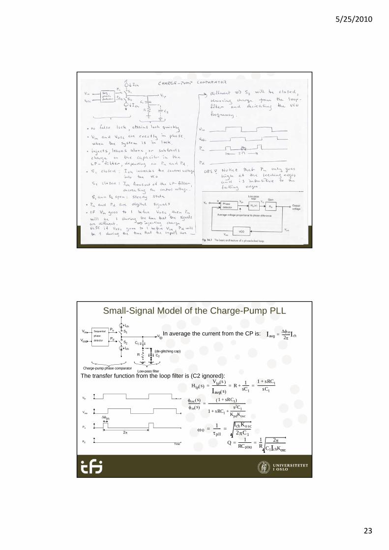
• dsdsd
Small-Signal Model of the Charge-Pump PLL
Iavgin
2-----------Ich=In average the current from the CP is:
Sequential
phase detector
Vin
Vosc
Pu
Pd
Ich
S1
S2 C1
R C2
Ich
Vlp
(de-glitching cap)
Hlp s Vlp s
Iavg s ------------------ R
1sC1---------+
1 sRC1+
sC1----------------------= = =
osc s in s ----------------
1 sRC1+
1 sRC1
s2C1
KpdKosc--------------------+ +
--------------------------------------------------=
The transfer function from the loop filter is (C2 ignored):Low-pass filter
Charge-pump phase comparator
Vin
Vosc
in
Pu
Pd
2
in
Time
01pll--------
Ich Ko sc
2C1-----------------= =
Q1
RC10----------------- 1
R---- 2
C1IchKosc
--------------------------= =

5/25/2010
24
Exam, Thursday 3rd of June• Individual written exam, counts 60 % (proj.:40 %) Both parts need not be
above “E” level to pass.. (ex: 0.4 * 60 % + 0.6 * 30 % = 24 % + 18 % = 42 % = “E”)
• 3 hours. Find exact time and place yourselves..• Questions based on material from the book, and from lectures, including
itt t i lwritten material.• You may bring any written material like for example books, papers and lecture
notes.• Consider writing at least something reasonable even if you feel that you don’t
know much about a given problem, as no answer means 0 points. A blank answer may have a bad impact on the average score.
• Read through all problems in the beginning. Your subconscious mind may work on the problems while you don’t noticework on the problems while you don t notice
• Parts of what I thought was important in the lectures, I probably think is important for the exam..
• Snorre will visit after about 30 minutes, and once later. Phone: 90013264
• Thanks for now, and good luck!