Subject: AITSDS/ECD/EXPT
27
ATMIYA INSTITUTE OF TECHNOLOGY & SCIENCE FOR DIPLOMA STUDIES, RAJKOT Subject: BE To study CRO. 1 Experiment No. 1. DATE: DOC. CODE AITSDS/ECD/EXPT/ CRO AIM:- To study the use of Cathode Ray Oscilloscope (CRO). Apparatus: - C.R.O, Connecting probe (BNC cable). Theory:- An CRO is easily the most useful instrument available for testing circuits at different points. The best way to investigate any electronic circuit is to monitor or check signal at input and output of each block, if they are correctly linked or not to next stage. The function of CRO is to draws graph of voltage against time (V/t), in that voltage is on vertical or Y-axis and time is on horizontal or X-axis. There are 8 squares or division on the X-axis and 10 squares on the Y-axis. The squares are of 1cm in each direction. FIGURE :-
Transcript of Subject: AITSDS/ECD/EXPT

ATMIYA INSTITUTE OF TECHNOLOGY & SCIENCE FOR DIPLOMA STUDIES, RAJKOT
Subject:
BE
To study CRO.
1
Experiment No.
1.
DATE:
DOC. CODE
AITSDS/ECD/EXPT/
CRO AIM:- To study the use of Cathode Ray Oscilloscope (CRO).
Apparatus: - C.R.O, Connecting probe (BNC cable).
Theory:-
An CRO is easily the most useful instrument available for testing circuits at different points. The
best way to investigate any electronic circuit is to monitor or check signal at input and output of each
block, if they are correctly linked or not to next stage.
The function of CRO is to draws graph of voltage against time (V/t), in that voltage is on vertical
or Y-axis and time is on horizontal or X-axis. There are 8 squares or division on the X-axis and 10
squares on the Y-axis. The squares are of 1cm in each direction.
FIGURE :-

ATMIYA INSTITUTE OF TECHNOLOGY & SCIENCE FOR DIPLOMA STUDIES, RAJKOT
Subject:
BE
To study CRO.
2
Experiment No.
1.
DATE:
DOC. CODE
AITSDS/ECD/EXPT/
Panel Control :-
Switch
No. Switch Use
1 Power On/Off Push button switch to supplying power to instrument.
2 X 10 MAG When pushed, gives 10 times magnification of the X
signal.
3 XY
4 CH-1 / CH-2 Select between channel 1 (when out) and channel 2
(when pressed)
5 Mono/Dual Selects Mono or Dual trace option.
6 ALT/CHOP/ADD
Selects alternate or chopped in dual mode and enable
for addition or subtraction of channel in mono mode
i.e CH-1± CH-2.
7 EXT. When pressed allows external triggering signal to be
fed.
8 Line When pressed displayed signal is synchronized with
mains line frequency.
9 ALT Selects alternate trigger mode from Ch1 and Ch2. In
this mode both the signals are synchronized.
10 +/- Selects the slope of triggering whether it is positive
going or negative going.
11 AT/NORM
12 Level Controls the trigger level from peak to peak amplitude
of signal.
13 Component tester When pressed starts component testing operation.
14 Pilot Lamp When glow indicates power ON position.
15 X-POS Controls horizontal position of the trace.
16 TB-VAR Controls time speed between two steps of Time/Div
switch, for calibration put it fully anticlockwise.
17 Trace Sep Separate traces X1 & X10 in 4 trace operation.
18 HOLD Off Controls Hold Off time between sweeps used for stable
triggering.
19 TRIG. INP To feed external trigger signal in EXT(external)
Trigger mode.

ATMIYA INSTITUTE OF TECHNOLOGY & SCIENCE FOR DIPLOMA STUDIES, RAJKOT
Subject:
BE
To study CRO.
3
Experiment No.
1.
DATE:
DOC. CODE
AITSDS/ECD/EXPT/
20 Intens Controls the brightness of trace.
21 TR Controls alignment of the trace with graticule.
22 Focus Controls sharpness of trace.
23 DC/AC/GD Input coupling switch for each channel.
24 CH1(Y) & CH2(X) BNC connector serve as input connection for CH1 and
CH2.
25 Illume For switching ON/Off graticule illumination.
26 CALOUT Socket provided for square wave output 200mv
27 CT To test any component in CT mode, put one test probe
in this socket and another to ground.
28 INV CH2 When pressed invert polarity of CH2.
29 Digital Readout LCD window displays Volt/Div and Time/Div.
30 Y Pos I & II Controls Vertical Position of signal.
31 Volts/Div Selects Volt/Div step for CH1.
32 Volts/Div Selects Volt/Div step for CH2.
33 NOR/ALT Switch selects Normal or Alternately expanded
simulation position.
34 Time/Div Selects Time/Div step for CH1 and CH2.
Application :-
1) Measurement of magnitude of signal.
2) View different type of signal.
3) Measurement of voltage , time period , frequency of any waveform.
4) To test component.
5) Compare two signal.
6) Measurement of phase difference.
7) To test electronic circuit.
PROCEDURE :-
1) For measurement of Voltage :-
a) Calculate the number of division covered by the entire height of the waveform.

ATMIYA INSTITUTE OF TECHNOLOGY & SCIENCE FOR DIPLOMA STUDIES, RAJKOT
Subject:
BE
To study CRO.
4
Experiment No.
1.
DATE:
DOC. CODE
AITSDS/ECD/EXPT/
b) Check the volt/div setting.
c) Now multiply two quantities: number of division covered by signal and reading of
Volt/Div.
Amplitude = Number of Division X Voil/Div.
2) For measurement of Currents :-
A CRO is basically a voltage indicating device. For measuring current, it is passed
through a suitable known resistor. Then the potential development across this resistor is
measured and put that value in below equation and the current can be find.
I = V / R
Where, I= current
V= Voltage / potential difference
R= Resistance
3) For measurement of frequency :-
a) Calculate the number of division in horizontal direction that are covered by the 1
complete cycle of waveform.
b) Observe the reading of Time/Div on the CRO front panel.
c) Multiply both , thus
Time period = No. of division X Time/Div
Frequency = 1 / Time period
4) For measurement of Phase Difference :-
a) Put the CRO in dual mode.
b) Apply two signals to CH-1 and CH-2 respectively and adjust the waveform.
c) Measure the time for one complete cycle of the signal, call it T sec.
d) Measure the time difference between the starting points or any same points of the two
signals. Call it t sec.
e) Now the phase difference between two signal is,
Phase Difference = (360 X t) / T.
CONCLUSION :

ATMIYA INSTITUTE OF TECHNOLOGY & SCIENCE FOR DIPLOMA STUDIES, RAJKOT
Subject:
BE
To study FUNCTION GENERATOR
1
Experiment No.
2
DATE:
DOC. CODE
AITSDS/ECD/EXPT/
Function Generator: Apparatus :- C.R.O, Function Generator , BNC cable.
Theory:-
The Function generator is a device which is used to generate different kind of waveforms. These
waveforms are used to test different electronic circuit. the function generator is having frequency range
from 2Hz to 2MHz. It can generate different type of waveforms like Sine wave, Square wave, Saw tooth
Wave, Triangle Wave, Pulse Train etc.
Figure:
Panel Control :-
Switch
No. Switch Use
1 Power On/Off Push button switch to switch ON device.
2 Display 7 Segment LED display to see value of Frequency.
3 Duty Cycle To adjust On/OFF time period of square wave.

ATMIYA INSTITUTE OF TECHNOLOGY & SCIENCE FOR DIPLOMA STUDIES, RAJKOT
Subject:
BE
To study FUNCTION GENERATOR
2
Experiment No.
2
DATE:
DOC. CODE
AITSDS/ECD/EXPT/
4 Freq. Vari. Adjust to Vary frequency.
5 Amp. Vari Adjust to vary amplitude of signal.
6 DC offset To remove DC component form AC waveform.
7 Attenuation (40 db/20
db) To attenuate amplitude of signal.
8 FM ext ( max 2Vp-p ) To apply FM external input.
9 Frequency range Band selection to generate frequency from 2Hz to
2MHz.
10 Output (50Ω,20Vp-
p,O.C.) Connect output probe to this knob.
11 FM Press it to take external FM input.
Application :-
1) To generate different frequencies.
2) For modulation of any signal.
3) To provide different waveforms.
4) To test any electronic circuit.
PROCEDURE :-
1) Switch ON the power supply.
2) Now select the range of frequency between 2Hz to 200MHz.
3) To change types of waveform select the type.
4) To change frequency preciously just vary frequency variation probe.
5) To change amplitude of waveform vary amplitude variation button.
6) Also can change the duty cycle of waveform.
7) To change DC level of waveform vary DC offset.

ATMIYA INSTITUTE OF TECHNOLOGY & SCIENCE FOR DIPLOMA STUDIES, RAJKOT
Subject:
BE
To study FUNCTION GENERATOR
3
Experiment No.
2
DATE:
DOC. CODE
AITSDS/ECD/EXPT/
WAVEFORM :-
CONCLUSION :-

ATMIYA INSTITUTE OF TECHNOLOGY & SCIENCE FOR DIPLOMA STUDIES, RAJKOT
Subject:
BE
To test half wave rectifier
1
Experiment No.
03
DATE:
DOC. CODE
AITSDS/ECD/EXPT/
AIM:- To test half wave rectifier.
Apparatus :- Trainer kit, Variable Voltage DC regulated power supply, Digital Multimeter,
Connecting probes, CRO.
Theory:-
Rectification means conversion of AC into DC. Diode has characteristics such that it allows
current to flow in one direction i.e. only in forward biased condition. AC is a sinusoidal waveform as
shown in Figure. Using positive half cycle current increases from zero to peak value and returns to
zero according to sine wave properly. During negative half cycle current goes to peak and returns to
zero.
Half wave rectifier circuit using diode is shown in Figure. During positive half cycle of AC
diode is forward biased, so it conducts heavily and current flows through the load resistance. During
negative half cycle of AC diode is reverse biased so no current flows through the diode as well as
through load resistance. Only a very small leakage current flows through the circuit. Thus output
voltage appears only during positive half cycles and waveform of voltage across load resistance is as
shown in Figure 3. Peak inverse voltage (PIV) is the maximum voltage across diode reverse bias.
PIV is the same as the peak amplitude of the input voltage as shown in Figure 4.
PROCEDURE :-
1) Connect the circuit as shown in figure-1.
2) Connect the resistance of known value
3) Measure the voltage and observe waveform with the help of CRO.
4) Draw the waveform across diode, supply voltage and output.
CIRCUIT DIAGRAM :-

ATMIYA INSTITUTE OF TECHNOLOGY & SCIENCE FOR DIPLOMA STUDIES, RAJKOT
Subject:
BE
To test half wave rectifier
2
Experiment No.
03
DATE:
DOC. CODE
AITSDS/ECD/EXPT/
Waveform :-
OBSERVATION TABLE :-
CONCLUSION :-
SR
No. V(p-p) Vout (p) PIV = Vm
1.
2.
3.
4.
5.

ATMIYA INSTITUTE OF TECHNOLOGY & SCIENCE FOR DIPLOMA STUDIES, RAJKOT
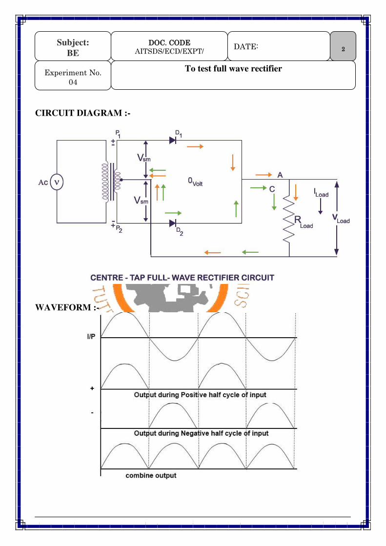
Subject:
BE
To test full wave rectifier
1
Experiment No.
04
DATE:
DOC. CODE
AITSDS/ECD/EXPT/
AIM:- To test full wave rectifier .
Apparatus :- Trainer kit, Digital Multimeter, Connecting probes, CRO.
Theory:-
In Full wave rectifier circuit, Center tapped transformer is used and two diodes are connected
as shown in Figure 1. During positive half cycle diode D1 conducts and current flows through the
load resistance. In this half cycle diode D2 is reverse biased and the maximum reverse voltage D2 is
the twice of the input peak voltage rating of the diode. During negative half cycle diode D2 conducts
and current flows through the load resistance in the same direction. In this half cycle diode D1
remains reverse biased.
Output from rectifier is pulsating DC. Most of the applications require smooth DC. This
output contains an AC portion, which is called ripple. Filters are used at output of rectifier to give
smooth DC without ripple.
A circuit in which capacitive filter is used as shown in Figure 1. During first quarter cycle in
which output is increasing, capacitor is charged to peak voltage. Then in second quarter cycle output
of rectifier decreases during that time capacitor discharges through the load resistance. But before
capacitor voltage discharges to zero, a next half cycle starts which again charges the capacitor. In this
way capacitive filter keeps the output voltage almost near to peak voltage by not allowing it to fall to
zero value. Thus ripples in rectifier output are filtered out by capacitance filter. Load resistance
provides path for capacitor discharge so it is also called bleeding resistance.
In capacitor filter circuit diodes do not conduct continuously. When output voltage from
transformer becomes larger than capacitor voltage, diode conducts. But most of the times diodes are
subjected to reverse voltage. Diodes must handle high peak current during recharging of capacitor for
a short period and this current increases with the value of capacitance. As the value of capacitor or
bleeding resistance increases ripple is reduced i.e. ripple factor is reduced. It means that load
resistance affects the ripple factor. Ripple factor is defined as the ratio of RMS value of AC
component present at output to DC voltage level at output.
PROCEDURE :-
1) Connect the circuit as shown in figure-1.
2) Connect voltmeter across load resistance.
3) Connect the C for capacitor load.
4) Turn ON the power supply
5) Measure voltage from voltmeter that is VDL and observe the output waveform..
6) Keep CRO in AC mode, measure the peak to peak voltage.
ATMIYA INSTITUTE OF TECHNOLOGY & SCIENCE FOR DIPLOMA STUDIES, RAJKOT
Subject:
BE
To test full wave rectifier
2
Experiment No.
04
DATE:
DOC. CODE
AITSDS/ECD/EXPT/
CIRCUIT DIAGRAM :-
WAVEFORM :-

ATMIYA INSTITUTE OF TECHNOLOGY & SCIENCE FOR DIPLOMA STUDIES, RAJKOT
Subject:
BE
To test full wave rectifier
3
Experiment No.
04
DATE:
DOC. CODE
AITSDS/ECD/EXPT/
OBSERVATION TABLE :-
SR
No. VDL Vp-p
1.
2.
3.
4.
5.
CONCLUSION :-

ATMIYA INSTITUTE OF TECHNOLOGY & SCIENCE FOR DIPLOMA STUDIES, RAJKOT
Subject:
BE
To test full wave rectifier bridge rectifier.
1
Experiment No.
05
DATE:
DOC. CODE
AITSDS/ECD/EXPT/
AIM:- To test full wave bridge rectifier .
Apparatus :- Trainer kit, Digital Multimeter, Connecting probes, CRO.
Theory:-
In Full wave rectifier circuit, Center tapped transformer is used and two diodes are connected
as shown in Figure 1. During positive half cycle diode D1 conducts and current flows through the
load resistance. In this half cycle diode D2 is reverse biased and the maximum reverse voltage D2 is
the twice of the input peak voltage rating of the diode. During negative half cycle diode D2 conducts
and current flows through the load resistance in the same direction. In this half cycle diode D1
remains reverse biased.
Output from rectifier is pulsating DC. Most of the applications require smooth DC.This output
contains an AC portion, which is called ripple. Filters are used at output of rectifier to give smooth
DC without ripple.
A circuit in which capacitive filter is used as shown in Figure 1. During first quarter cycle in
which output is increasing, capacitor is charged to peak voltage. Then in second quarter cycle output
of rectifier decreases during that time capacitor discharges through the load resistance. But before
capacitor voltage discharges to zero, a next half cycle starts which again charges the capacitor. In this
way capacitive filter keeps the output voltage almost near to peak voltage by not allowing it to fall to
zero value. Thus ripples in rectifier output are filtered out by capacitance filter. Load resistance
provides path for capacitor discharge so it is also called bleeding resistance.
In capacitor filter circuit diodes do not conduct continuously. When output voltage from
transformer becomes larger than capacitor voltage, diode conducts. But most of the times diodes are
subjected to reverse voltage. Diodes must handle high peak current during recharging of capacitor for
a short period and this current increases with the value of capacitance. As the value of capacitor or
bleeding resistance increases ripple is reduced i.e. ripple factor is reduced. It means that load
resistance affects the ripple factor. Ripple factor is defined as the ratio of RMS value of AC
component present at output to DC voltage level at output.
PROCEDURE :-
1) Connect the circuit as shown in figure-1.
2) Connect voltmeter across load resistance.
3) Connect the C for capacitor load.
4) Turn ON the power supply
5) Measure voltage from voltmeter that is VDL and observe the output waveform..
6) Keep CRO in AC mode, measure the peak to peak voltage.

ATMIYA INSTITUTE OF TECHNOLOGY & SCIENCE FOR DIPLOMA STUDIES, RAJKOT
Subject:
BE
To test full wave rectifier bridge rectifier.
2
Experiment No.
05
DATE:
DOC. CODE
AITSDS/ECD/EXPT/
CIRCUIT DIAGRAM :-
OBSERVATION TABLE :-
SR
No. VDL Vp-p
1.
2.
3.

ATMIYA INSTITUTE OF TECHNOLOGY & SCIENCE FOR DIPLOMA STUDIES, RAJKOT
Subject:
BE
To test full wave rectifier bridge rectifier.
3
Experiment No.
05
DATE:
DOC. CODE
AITSDS/ECD/EXPT/
WAVEFORM:-
CONCLUSION :-

ATMIYA INSTITUTE OF TECHNOLOGY & SCIENCE FOR DIPLOMA STUDIES, RAJKOT
Subject:
BE
TO STUDY P-N JUNCTION IN FORWARD BIAS
1
Experiment No.
6
DATE:
DOC. CODE
AITSDS/ECD/EXPT/
AIM: TO STUDY P-N JUNCTION IN FORWARD BIAS.
APPARATUS: Trainer kit, Variable voltage DC regulated power supply, Voltmeter,
Milli ammeter, Micro ammeter, connecting probes.
THEORY:
When diode is connected in such a way that its P terminal is connected with positive terminal of
battery and N terminal is connect to negative terminal of battery. Diode is forward bias is shown in
fig.2 in forward bias. Diode allows large current to flow in the circuit and voltage is developed across
resistance R1. As supply voltage is increased. Voltage across resistance increases because once diode
is turned on. The voltage across diode does not change appreciably. In forward bias the voltage across
diode is about 0.3V for germanium diode and 0.7V for a silicon diode. The reminder of the applied
voltage appears the resistor connected in series of the diode.
Circuit Diagram:
PROCEDURE:
1. Note down maximum forward current and peak inverse voltage of the diode given by
manufacturer.
2. Connect the circuit as shown in fig.
3. Increase the supply voltage in small steps and measure the current passing through the circuit as
well as voltage across diode. Note down the readings in table.
4. Plot forward current Vs forward voltage.

ATMIYA INSTITUTE OF TECHNOLOGY & SCIENCE FOR DIPLOMA STUDIES, RAJKOT
Subject:
BE
TO STUDY P-N JUNCTION IN FORWARD BIAS
2
Experiment No.
6
DATE:
DOC. CODE
AITSDS/ECD/EXPT/
OBSERVATION TABLE:
Sr.
No. Forward current Forward voltage Reverse current Reverse voltage
V-I characteristic:
CONCLUSION:

ATMIYA INSTITUTE OF TECHNOLOGY & SCIENCE FOR DIPLOMA STUDIES, RAJKOT
Subject:
BE
Obtain the V-I characteristic of zener diode.
1
Experiment No.
07
DATE:
DOC. CODE
AITSDS/ECD/EXPT/
AIM: - Obtain the V-I characteristic of zener diode.
Apparatus: - Trainer kit, Variable Voltage DC regulated power supply, Digital Multimeter, Connecting
probes.
Theory:-
Normal P-N junction diode, in reverse bias carries large amount of current ,so large amount of
power dissipation occurs that damage the P-N junction diode, so does not used in reverse bias. While
Zener diode is highly doped compare to P-N junction diode so it can be used in reverse bias region.
Symbol of Zener diode is shown in Figure-1.
Characteristic of voltage V/S current of zener diode is shown in figure-2. In forward bias zener
diode is same as forward characteristic of normal P-N junction diode. When the diode is reverse-biased, a
small reverse current is remains relatively constant despite an increase in reverse bias, until the Zener
breakdown region, in the vicinity of the Zener voltage Vz, is reached. In this vicinity reverse current starts
rising rapidly because of avalanche effect. Finally Zener breakdown occurs when the Zener voltage Vz is
reached. Zener breakdown need not result in the destruction of the diode.
CIRCUIT DIAGRAM :-
If
(mA)
Vz (v) Vf (v)
Iz
(mA)
Figure 2. Characteristic of Zener Diode

ATMIYA INSTITUTE OF TECHNOLOGY & SCIENCE FOR DIPLOMA STUDIES, RAJKOT
Subject:
BE
Obtain the V-I characteristic of zener diode.
2
Experiment No.
07
DATE:
DOC. CODE
AITSDS/ECD/EXPT/
PROCEDURE :-
1) Connect the circuit as shown in figure-3.
2) Connect regulated DC power supply of 0-18v.
3) Turn ON the power supply and increase slowly supply voltage and measure and note down zener
voltage Vz and zener current Iz.
4) Plot characteristic graph of zener voltage versus zener current.
OBSERVATION TABLE :-
Sr.
No.
Forward Bias Reverse Bias
Diode Voltage Forward
Current
Diode
Voltage
Reverse current
1. 0.1v 0.5v
2. 0.2v 1v
3. 0.3v 1.5v
4. 0.4v 2v
5. 0.5v 3v
6. 0.6v 4v
7. 0.7v 5v
8. 0.8v 6v
9. 0.9v 7v
CONCLUSION :-

ATMIYA INSTITUTE OF TECHNOLOGY & SCIENCE FOR DIPLOMA STUDIES, RAJKOT
Subject:
BE
To Study Filter
1
Experiment No.
8
DATE:
DOC. CODE
AITSDS/ECD/EXPT/
AIM: To Study Filter.
Apparatus : Trainer kit, CRO, Connecting probes
Theory :
The circuit diagram of the bridge rectifier with filter capacitor is shown in the following figure. When
capacitor charges during the first cycle, surge current flows because initially capacitor acts like a short
circuit. Thus, surge current is very large. If surge current exceeds rated current capacity of the diode it
can damage the diode. To limit surge current surge resistance is used in series as shown in the figure.
Similar surge resistance can be used in half wave as well as center-tapped full wave rectifier also.
Circuit Diagram:
Bridge rectifier package (combination of four diodes in form of bridge) is easily available in the market
for various current capacities ranging from 500 mA to 30A. For laboratory purpose you can use 1A
package.
Advantages:
No center tap is required in the transformer secondary hence transformer design is simple. If
stepping up and stepping down not required than transformer can be eliminated. (In SMPS used
in TV and computer, 230V is directly applied to the input of bridge rectifier).
The PIV of the diode is half than in center tap full wave rectifier
Transformer utilization factor is higher than in center tapped full wave rectifier
Smaller size transformer required for given capacity because transformer is utilized effectively
during both AC cycles.
Disadvantages:
Requires Four diodes (But package is low cost)
Forward voltage drop across two diodes. This will reduce efficiency particularly when low
voltage (less than 5V ) is required.
Load resistance and supply source have no common point which may be earthed.

ATMIYA INSTITUTE OF TECHNOLOGY & SCIENCE FOR DIPLOMA STUDIES, RAJKOT
Subject:
BE
To Study Filter
2
Experiment No.
8
DATE:
DOC. CODE
AITSDS/ECD/EXPT/
Waveform:
Conclusion:

ATMIYA INSTITUTE OF TECHNOLOGY & SCIENCE FOR DIPLOMA STUDIES, RAJKOT
Subject:
BE
TO BUILD AND TEST COLPITTS OSCILLATOR.
1
Experiment No.
09
.
DATE:
DOC. CODE
AIM: TO BUILD AND TEST COLPITTS OSCILLATOR.
Apparatus : Oscilloscope, +12V DC Adapter, Patch Cords.
Circuit Diagram :
Procedure :
1. Connect +12V DC Supply (adapter) to the trainer
2. Now connect +12V terminal to TP2 and Gnd to Gnd as shown in figure.
3. Connect terminals 1 and 2 and similarly 4 and Gnd together.
4. Switch ‘On’ the mains supply. 5. Connect oscilloscope between Vout and Gnd.
6. Measure the value of output frequency on oscilloscope.
7. Calculate the resonance frequency (theoretical) using equation 1.
8. Compare measured frequency with the theoretically calculated value.
9. Switch ‘Off’ the supply.
ATMIYA INSTITUTE OF TECHNOLOGY & SCIENCE FOR DIPLOMA STUDIES, RAJKOT
Subject:
BE
TO BUILD AND TEST COLPITTS OSCILLATOR.
2
Experiment No.
09
.
DATE:
DOC. CODE
Observation Table:
SR. NO. Capacitors Ceq.
(Equivalent
Capacitance)
Output
frequency
(Measured)
Output
frequency
(Theoretical)
CONCLUSION:

ATMIYA INSTITUTE OF TECHNOLOGY & SCIENCE FOR DIPLOMA STUDIES, RAJKOT
Subject:
BE
TO BUILD AND TEST HARTELY OSCILLATOR.
1
Experiment No.
10
.
DATE:
DOC. CODE
AIM: TO BUILD AND TEST HARTELY OSCILLATOR.
APPARATUS: Power Supply.
Trainer kit,
Connecting probe,
CRO.
THEORY: Any circuit generates an alternating voltage is called an oscillator. To generate AC voltage, the circuit. is
supplied energy from a DC source. Main application of positive feedback is oscillator. If output signal varies
sinusoidally, the circuit is referred to as a sinusoidal oscillator. If output voltage rises quickly to one voltage
level and later drops quickly to another voltage level, the circuit. is generally referred to as a pulse or square
wave oscillator.
Consider the feedback circuit, which is shown in the fig. When the switch at the amplifier input is open, no
oscillation occurs. Consider that we have a input (Vi). This results in an output voltage Vo = AVi after the
amplifier stage and in a voltage Vf = B (AVi) after the feed back stage. Thus, we have a feedback voltage Vf =
BAVi where BA is referred to as the loop gain if the circuit of the base amplifier and feedback network provide
BA of correct magnitude and phase, Vf can be made equal to Vi. Then when the switch is closed and voltage Vi
is removed, the circuit will continue operating since the feedback voltage is sufficient to drive the amplifier and
feedback circuit resulting in a proper input voltage to sustain the loop operation. The output waveform will still
exist after the switch is closed.
We derive the expression for the over all voltage gain of the amp. can be written as
Af=A/1-A.
It can now be seen that if AB =1, so Af= . The gain becoming infinity means that there is a output without any
input. In other words, the amp. Becomes an oscillator. The condition,
AB=1 is known as barkhausen critetion of oscillation.
As shown in the fig. of Hartley oscillator, two inductors L1 &L2 are placed across a capacitor C. Frequency is
determine by L1,L2 and C (tank circuit).
When the circuit is turned ON, the capacitor is charged. When this capacitor is fully charged it discharges
through coils L1 and L2.The output voltage of the ampere appears across L1 and feedback voltage across L2.
The voltage across L2 is 180 out of phase with the voltage developed across L1. It is easy to see that voltage
feedback to the transistor provides positive feedback. A phase shift of 180 is produced by the transistor and the
L1-L2 voltage divider produces further phase shift of 180, in this way feedback is continuous un-damped
oscillation.
PROCEDURE: 1. Assemble the circuit as shown in the fig.
2. Connect the CRO at the output terminals and observed the sine wave output.
3. Measure the output frequency on CRO.
OBSERVATION TABLE:
No. Inductor
(L)
Capacitor
(C1)
Capacitor
(C2)
Observed
frequency
Theoretical
frequency
1.
2.
3.

ATMIYA INSTITUTE OF TECHNOLOGY & SCIENCE FOR DIPLOMA STUDIES, RAJKOT
Subject:
BE
TO BUILD AND TEST HARTELY OSCILLATOR.
2
Experiment No.
10
.
DATE:
DOC. CODE
Circuit diagram:
CONCLUSION:

ATMIYA INSTITUTE OF TECHNOLOGY & SCIENCE FOR DIPLOMA STUDIES, RAJKOT
Subject:
BE
To understand working of transistor as a switch.
1
Experiment No.
11
DATE:
DOC. CODE
AITSDS/ECD/EXPT/
AIM: To understand working of transistor as a switch.
Introduction: Transistor can be operated in three region: cut-off region, active region and saturation region. While
using transistor in amplifier circuit, we are using active region. If transistor operated in cut-off and
saturation region in amplifier, clipping of waveforms will occur. When we use transistor as a switch,
only two regions cut-off and saturation are used. In saturation region transistor acts as ON switch. In cut-
off region, transistor acts as OFF switch. We are using only two points of DC load line while using
transistor as a switch.
Circuit diagram:
Experiment Procedure to obtain input characteristics:
Connect circuit as shown in the circuit diagram for input characteristics
Adjust collector supply Vcc = +12V and base supply VBB=+5V
You may use base voltage supply switch instead of switch shown in the circuit diagram.
Measure base current when switch is OFF (It will be zero). Measure collector current and voltage
between collector and emitter. LED is off because transistor is in cut-off region,
Now apply base voltage +5V, LED will be ON. Measure collector current and collector-emitter
voltage. Transistor is in saturation region.

ATMIYA INSTITUTE OF TECHNOLOGY & SCIENCE FOR DIPLOMA STUDIES, RAJKOT
Subject:
BE
To understand working of transistor as a switch.
2
Experiment No.
11
DATE:
DOC. CODE
AITSDS/ECD/EXPT/
Observations:
[1] Switch off (VBB=0): Ib = _________ VCE = __________ Ic = ________
[2] Switch ON (VBB=+5V): Ib = _________ VCE = __________ Ic = ________
Conclusion: