SUB-MICRON TECHNOLOGY DEVELOPMENT AND SYSTEM-ON …eprints.utm.my/id/eprint/2919/1/72319.pdf ·...
59
SUB-MICRON TECHNOLOGY DEVELOPMENT AND SYSTEM-ON-CHIP (SoC) DESIGN - DATA COMPRESSION CORE NASIR SHAIKH HUSIN Final Report for IRPA Vot 72319 Fakulti Kejuruteraan Elektrik Universiti Teknologi Malaysia DECEMBER 2002
Transcript of SUB-MICRON TECHNOLOGY DEVELOPMENT AND SYSTEM-ON …eprints.utm.my/id/eprint/2919/1/72319.pdf ·...
SUB-MICRON TECHNOLOGY DEVELOPMENT AND SYSTEM-ON-CHIP
(SoC) DESIGN - DATA COMPRESSION CORE
NASIR SHAIKH HUSIN
Final Report for IRPA Vot 72319
Fakulti Kejuruteraan Elektrik
Universiti Teknologi Malaysia
DECEMBER 2002

ii
ABSTRACT
Data compression removes redundancy from the source data and thereby
increases storage capacity of a storage medium or efficiency of data transmission in a
communication link. Although several data compression techniques have been
implemented in hardware, they are not flexible enough to be embedded in more
complex applications. Data compression software meanwhile cannot support the
demand of high-speed computing applications. Due to these deficiencies, in this
project we develop a parameterized lossless universal data compression IP core for
high-speed applications. The design of the core is based on the combination of
Lempel-Ziv-Storer-Szymanski (LZSS) compression algorithm and Huffman coding.
The resulting IP core offers a data-independent throughput that can process a symbol
in every clock cycle. The design is described in parameterized VHDL code to enable
a user to make a suitable compromise between resource constraints, operation speed
and compression saving, so that it can be adapted for any target application. In
implementation on Altera FLEX10KE FPGA device, the design offers a performance
of 800 Mbps with an operating frequency of 50 MHz. This IP core is suitable for
high-speed computing applications or for storage systems.

iii
ABSTRAK
Pemampatan data menyingkirkan lelebihan dari sumber data dan dengan itu
meningkatkan keupayaan simpanan sesuatu bahantara storan atau kecekapan
penghantaran data dalam sesuatu kait perhubungan. Walaupun beberapa teknik
pemampatan data telah dilaksanakan dalam perkakasan, mereka tidak mudah diubah
suai untuk digunakan di dalam aplikasi yang lebih kompleks. Perisian pemampatan
data pula tidak boleh menyokong keperluan aplikasi perkomputeran kelajuan tinggi.
Oleh kerana kekurangan tersebut, dalam projek ini kami membina satu teras IP
pemampatan data tanpa-kehilangan berparameter yang semesta untuk aplikasi
kelajuan tinggi. Rekabentuk teras adalah berdasarkan gabungan algoritma
pemampatan Lempel-Ziv-Storer-Szymanski (LZSS) dan pengekodan Huffman. Teras
IP yang dihasilkan mempunyai celusan yang tidak bergantung pada data dan boleh
memproses satu simbol dalam setiap kitar jam. Rekabentuk teras ditulis dalam kod
VHDL berparameter untuk membolehkan pengguna membuat kompromi yang sesuai
diantara kekangan komponen, kelajuan operasi dan penjimatan pemampatan, supaya
ia dapat disesuaikan untuk sebarang aplikasi sasaran. Berdasarkan pelaksanan dalam
peranti FPGA FLEX10KE Altera, rekabentuk ini mempunyai prestasi 800 Mbps
dengan frekuensi pengendalian 50 MHz. Teras IP ini adalah sesuai untuk aplikasi
perkomputeran kelajuan tinggi atau untuk sistem storan.

iv
TABLE OF CONTENTS
CHAPTER TITLE PAGE
ABSTRACT ii
ABSTRAK iii
TABLE OF CONTENTS iv
LIST OF TABLES vii
LIST OF FIGURES viii
LIST OF ABBREVIATIONS ix
CHAPTER I INTRODUCTION 1
1.1 Problem Statement
1.2 Objectives
1.3 Scope of Work
1.4 Contributions of the Research
1.5 Organization of Report
1.6 Summary
2
3
3
4
5
6
CHAPTER II LITERATURE REVIEW 7
2.1 Data Compression Background
2.2 Data Compression Algorithms
2.3 Previous work on Implementations of Data
Compression
2.4 Reconfigurability and Reusability
2.5 Systolic Architecture for LZ77/LZSS
2.6 Discussion and Summary
7
8
9
10
11
12

v
CHAPTER III METHODOLOGIES AND TOOLS 14
3.1 Research Procedure
3.2 Timing Simulation in Design Verification
3.3 Hardware Evaluation System for Test and
Performance Analysis
3.4 Hardware and Software Tools
3.5 Discussion and Summary
14
15
15
17
18
CHAPTER IV DESIGN OF DATA COMPRESSION
HARDWARE
19
4.1 Overview of Compression Hardware System
4.2 Design of Compression Core
4.3 Compression Interface Controller
4.4 Design of Decompression Core
4.5 Decompression Interface Controller
4.6 Summary
19
21
22
23
24
24
CHAPTER V DESIGN VERIFICATION AND PERFORMANCE
ANALYSIS
25
5.1 Design Verification
5.1.1 Results of Timing Simulation
5.1.2 Results of Hardware Test
5.2 Performance Analysis
5.2.1 Performance Metrics Applied
5.2.2 Performance Analysis – Clock Speed
and Area
5.2.3 Performance Analysis – Compression
Ratio
25
26
26
27
28
29
30

vi
5.2.4 Performance Analysis – Comparison
with Other Implementations
5.3 Summary
32
33
CHAPTER VI CONCLUSIONS 34
6.1 Concluding Remarks
6.2 Future Work
34
35
REFERENCES 37

CHAPTER I
INTRODUCTION
This project is a collaboration project between MIMOS, which acted as the
Project Leader, and Universiti Teknologi Malaysia, Universiti Putra Malaysia,
Universiti Sains Malaysia and Universiti Malaya. The main objective of the project is
to develop a 0.35-micron integrated circuit (IC) fabrication technology. MIMOS can
already fabricate ICs using 0.8-micron technology. However, this technology is
several generations behind state of the art fabrication process. With this project, the
gap can be reduced. The current state of the art fabrication technology is 0.15-micron
process. All current processes are called sub-micron processes because the smallest
feature that can be fabricated is less than 1 micron.
When the fabrication process is successfully upgraded, local research
institutions or companies can contract with MIMOS to fabricate their designs. To
help these clients, MIMOS must have many sub-system designs, ready to be
embedded by clients into their applications. These sub-systems should be in the form
of IP (intellectual property) cores, where the design is described in a hardware design
language like VHDL, and must be parameterizable so that customers can easily
modify the cores to suit their applications. For organizations that do not want to
fabricate their design, they can also use FPGA (Field Programmable Gate Array.)
The FPGA devices nowadays can accommodate really large designs, integrating
many sub-systems into a single device. These new FPGA devices give rise to so-
called SoC (Silicon-on-Chip) design methodology, where sub-system integration and
software interfacing have to be given serious consideration. The entire project is
distributed as follows:

2
MIMOS (Project Leader) is responsible for sub-micron process development
and device design.
UTM is responsible for IP core design and SoC design methodology.
UPM is responsible for sub-micron process and device simulations.
USM is responsible for process development test and characterization.
UM is also responsible for core design.
UTM chose to develop data compression IP core. The objective is to produce
a reusable data compression core such that a user can choose to compromise between
resource constraints, speed and compression level to suit a variety of high-speed
applications. The design is based on Lempel-Ziv-Storer-Szymanski (LZSS)
compression algorithm combined with Huffman coding. The rest of this report
describes the development of this data compression core. In this chapter, the
challenge of data compression implementation is discussed. The objective and scope
of this work is also presented.
1.1 Problem Statement
Data compression is a cost-effective way to increase the effective
communication bandwidth or the effective storage capacity without significant
increment in cost. It removes redundant information inherent in the source data,
thereby enabling a communication link to transmit the same amount of data in fewer
bits. For storage systems, fewer bits are actually stored thus increasing the effective
storage capacity.
The compression core must be able to handle any kind of source data so that
it can be used in real-world applications. The implementation has to be fast enough
to satisfy high-speed applications. Finally, the design must not be too complicated
such that hardware requirements are too excessive.
Several data compression techniques have been implemented in either
software or hardware. Data compression software, which runs on a personal

3
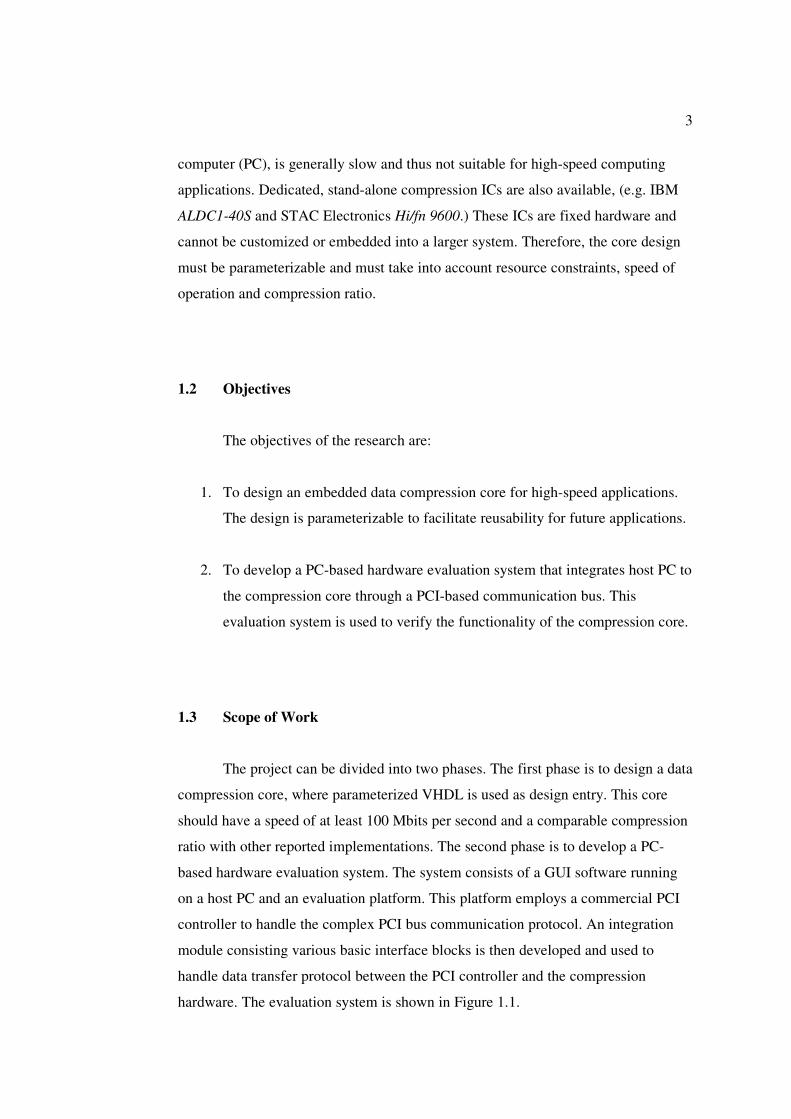
computer (PC), is generally slow and thus not suitable for high-speed computing
applications. Dedicated, stand-alone compression ICs are also available, (e.g. IBM
ALDC1-40S and STAC Electronics Hi/fn 9600.) These ICs are fixed hardware and
cannot be customized or embedded into a larger system. Therefore, the core design
must be parameterizable and must take into account resource constraints, speed of
operation and compression ratio.
1.2 Objectives
The objectives of the research are:
1. To design an embedded data compression core for high-speed applications.
The design is parameterizable to facilitate reusability for future applications.
2. To develop a PC-based hardware evaluation system that integrates host PC to
the compression core through a PCI-based communication bus. This
evaluation system is used to verify the functionality of the compression core.
1.3 Scope of Work
The project can be divided into two phases. The first phase is to design a data
compression core, where parameterized VHDL is used as design entry. This core
should have a speed of at least 100 Mbits per second and a comparable compression
ratio with other reported implementations. The second phase is to develop a PC-
based hardware evaluation system. The system consists of a GUI software running
on a host PC and an evaluation platform. This platform employs a commercial PCI
controller to handle the complex PCI bus communication protocol. An integration
module consisting various basic interface blocks is then developed and used to
handle data transfer protocol between the PCI controller and the compression
hardware. The evaluation system is shown in Figure 1.1.

4
Figure 1.1: Evaluation System
The implementation for this project is limited to Altera devices only. This is
because of the usage of Altera LPM modules to instantiate RAM and FIFO. For
implementations other than Altera devices, all the LPM modules should be replaced
with equivalent modules in the particular chosen device.
1.4 Contributions of the Research
This research work has led to the following outcomes:
1. The development of a parameterizable data compression embedded core with
a competitive performance, compared to other high-performance ASIC or
FPGA data compression hardware. It can process a symbol with a clock
speed of 50 MHz and offer a data-independent throughput of 50 Msymbols
per second. Since the design is parameterizable, it can be easily interfaced
Host PC
PCI Driver
GUI
Program
PCI Plug-In Card
EVALUATION PLATFORM
PCI Controller
Compression
Core
Integration
Module
PCI BUS

5
with any system and enable a user to choose a suitable compromise between
resource constraints, speed and compression ratio.
2. The development of a PC-based hardware evaluation system that allows a
host PC to access the hardware resources in the compression coprocessor via
the PCI communication bus interface. This evaluation system facilitates
verification of the coprocessor design.
3. With a suitable arrangement of compression and decompression units in an
embedded core environment, we can obtain a real-time data compression
system that can work in either half-duplex or full-duplex processing.
1.5 Organization of Report
This report is organized into six chapters. The first chapter introduces the
motivation of this research. Chapter II contains the literature review to support the
rationale behind this work and also to search for the solutions to the research
problem.
Chapter III describes the methodologies for this project where design
verification methods, tools and techniques used in this project are described. Chapter
IV presents the hardware design of the data compression core. Chapter V reports the
results obtained after testing the designed core. The results are analyzed to validate
the compression core design. The performance analysis of the core is also included in
this chapter. Finally, the last chapter summarizes the research findings and suggests
potential future work.

6
1.6 Summary
This chapter provides an overview of the project. The challenge of the data
compression implementation is discussed, and the objectives for the project are
identified.

SUB-MICRON TECHNOLOGY DEVELOPMENT AND SYSTEM-ON-CHIP
(SoC) DESIGN - DATA COMPRESSION CORE
NASIR SHAIKH HUSIN
Final Report for IRPA Vot 72319
Fakulti Kejuruteraan Elektrik
Universiti Teknologi Malaysia
DECEMBER 2002

ii
ABSTRACT
Data compression removes redundancy from the source data and thereby
increases storage capacity of a storage medium or efficiency of data transmission in a
communication link. Although several data compression techniques have been
implemented in hardware, they are not flexible enough to be embedded in more
complex applications. Data compression software meanwhile cannot support the
demand of high-speed computing applications. Due to these deficiencies, in this
project we develop a parameterized lossless universal data compression IP core for
high-speed applications. The design of the core is based on the combination of
Lempel-Ziv-Storer-Szymanski (LZSS) compression algorithm and Huffman coding.
The resulting IP core offers a data-independent throughput that can process a symbol
in every clock cycle. The design is described in parameterized VHDL code to enable
a user to make a suitable compromise between resource constraints, operation speed
and compression saving, so that it can be adapted for any target application. In
implementation on Altera FLEX10KE FPGA device, the design offers a performance
of 800 Mbps with an operating frequency of 50 MHz. This IP core is suitable for
high-speed computing applications or for storage systems.

iii
ABSTRAK
Pemampatan data menyingkirkan lelebihan dari sumber data dan dengan itu
meningkatkan keupayaan simpanan sesuatu bahantara storan atau kecekapan
penghantaran data dalam sesuatu kait perhubungan. Walaupun beberapa teknik
pemampatan data telah dilaksanakan dalam perkakasan, mereka tidak mudah diubah
suai untuk digunakan di dalam aplikasi yang lebih kompleks. Perisian pemampatan
data pula tidak boleh menyokong keperluan aplikasi perkomputeran kelajuan tinggi.
Oleh kerana kekurangan tersebut, dalam projek ini kami membina satu teras IP
pemampatan data tanpa-kehilangan berparameter yang semesta untuk aplikasi
kelajuan tinggi. Rekabentuk teras adalah berdasarkan gabungan algoritma
pemampatan Lempel-Ziv-Storer-Szymanski (LZSS) dan pengekodan Huffman. Teras
IP yang dihasilkan mempunyai celusan yang tidak bergantung pada data dan boleh
memproses satu simbol dalam setiap kitar jam. Rekabentuk teras ditulis dalam kod
VHDL berparameter untuk membolehkan pengguna membuat kompromi yang sesuai
diantara kekangan komponen, kelajuan operasi dan penjimatan pemampatan, supaya
ia dapat disesuaikan untuk sebarang aplikasi sasaran. Berdasarkan pelaksanan dalam
peranti FPGA FLEX10KE Altera, rekabentuk ini mempunyai prestasi 800 Mbps
dengan frekuensi pengendalian 50 MHz. Teras IP ini adalah sesuai untuk aplikasi
perkomputeran kelajuan tinggi atau untuk system storan.

iv
TABLE OF CONTENTS
CHAPTER TITLE PAGE
ABSTRACT ii
ABSTRAK iii
TABLE OF CONTENTS iv
LIST OF TABLES vii
LIST OF FIGURES viii
LIST OF ABBREVIATIONS ix
CHAPTER I INTRODUCTION 1
1.1 Problem Statement
1.2 Objectives
1.3 Scope of Work
1.4 Contributions of the Research
1.5 Organization of Report
1.6 Summary
2
3
3
4
5
6
CHAPTER II LITERATURE REVIEW 7
2.1 Data Compression Background
2.2 Data Compression Algorithms
2.3 Previous work on Implementations of Data
Compression
2.4 Reconfigurability and Reusability
2.5 Systolic Architecture for LZ77/LZSS
2.6 Discussion and Summary
7
8
9
10
11
12
v
CHAPTER III METHODOLOGIES AND TOOLS 14
3.1 Research Procedure
3.2 Timing Simulation in Design Verification
3.3 Hardware Evaluation System for Test and
Performance Analysis
3.4 Hardware and Software Tools
3.5 Discussion and Summary
14
15
15
17
18
CHAPTER IV DESIGN OF DATA COMPRESSION
HARDWARE
19
4.1 Overview of Compression Hardware System
4.2 Design of Compression Core
4.3 Compression Interface Controller
4.4 Design of Decompression Core
4.5 Decompression Interface Controller
4.6 Summary
19
21
22
23
24
24
CHAPTER V DESIGN VERIFICATION AND PERFORMANCE
ANALYSIS
25
5.1 Design Verification
5.1.1 Results of Timing Simulation
5.1.2 Results of Hardware Test
5.2 Performance Analysis
5.2.1 Performance Metrics Applied
5.2.2 Performance Analysis – Clock Speed
and Area
5.2.3 Performance Analysis – Compression
Ratio
25
26
26
27
28
29
30
vi
5.2.4 Performance Analysis – Comparison
with Other Implementations
5.3 Summary
32
33
CHAPTER VI CONCLUSIONS 34
6.1 Concluding Remarks
6.2 Future Work
34
35
REFERENCES 37

vii
LIST OF TABLES
TABLE NO TITLE PAGE
3.1 Compression Benchmark Data Set 16
5.1 Parameter Configuration of the PCI-Based Data
Compression Hardware Core
26
5.2 Standard Data Compression Benchmark Data
Sets
27
5.3 Latency of Compression Core 28
5.4 Latency of Decompression Core 29
5.5 Area and Speed Evaluation Results 30
5.6 Compression Ratio 31
5.7 Computation Time for Compression 31
5.8 Computation Time for Decompression 32
5.9 Comparison of Data Compression Hardware
using Text Data
33
6.1 Specifications of the Data Compression
Embedded Core
35

viii
LIST OF FIGURES
FIGURE NO TITLE PAGE
1.1 Evaluation System 4
2.1 Broadcast/Reduce Systolic Architecture 12
4.1 Compression System 20
4.2 Functional Block Diagram of the Compression
Subsystem
20
4.3 Functional Block Diagram of the
Decompression Subsystem
21
4.4 Block Diagram of Compression_Unit 21
4.5 Block Diagram of Compression_Interface 22
4.6 Block Diagram of Decompression_Unit 23
4.7 Block Diagram of Decompression_Interface 24

ix
LIST OF ABBREVIATIONS
API - Application Programming Interface
ASIC - Application Specific Integrated Circuit
CMOS - Complementary Metal Oxide Semiconductor
EAB - Embedded Array Block
FIFO - First In First Out
FLEX - Flexible Logic Element MatriX
FPGA - Field Programmable Gate Array
GUI - Graphic User Interface
I/O - Input/Output
IC - Integrated Circuit
IP - Intellectual Property
JTAG - Joint Action Test Group
LC - Logic Cell
LE - Logic Element
LPM - Library of Parameterized Modules
LZ - Lempel-Ziv
LZ77 - Lempel-Ziv-77
LZSS - Lempel-Ziv-Storer-Szymanski
OS - Operating System
PC - Personal Computer
PCI - Peripheral Component Interconnect
PE - Processing Element
RAM - Random Access Memory
SoC - System on Chip
UTM - Universiti Teknologi Malaysia
VHDL - Very high speed integrated circuit Hardware Description Language
VLSI - Very Large Scale Integration
CHAPTER I
INTRODUCTION
This project is a collaboration project between MIMOS, which acted as the
Project Leader, and Universiti Teknologi Malaysia, Universiti Putra Malaysia,
Universiti Sains Malaysia and Universiti Malaya. The main objective of the project is
to develop a 0.35-micron integrated circuit (IC) fabrication technology. MIMOS can
already fabricate ICs using 0.8-micron technology. However, this technology is
several generations behind state of the art fabrication process. With this project, the
gap can be reduced. The current state of the art fabrication technology is 0.15-micron
process. All current processes are called sub-micron processes because the smallest
feature that can be fabricated is less than 1 micron.
When the fabrication process is successfully upgraded, local research
institutions or companies can contract with MIMOS to fabricate their designs. To
help these clients, MIMOS must have many sub-system designs, ready to be
embedded by clients into their applications. These sub-systems should be in the form
of IP (intellectual property) cores, where the design is described in a hardware design
language like VHDL, and must be parameterizable so that customers can easily
modify the cores to suit their applications. For organizations that do not want to
fabricate their design, they can also use FPGA (Field Programmable Gate Array.)
The FPGA devices nowadays can accommodate really large designs, integrating
many sub-systems into a single device. These new FPGA devices give rise to so-
called SoC (Silicon-on-Chip) design methodology, where sub-system integration and
software interfacing have to be given serious consideration. The entire project is
distributed as follows:

2
MIMOS (Project Leader) is responsible for sub-micron process development
and device design.
UTM is responsible for IP core design and SoC design methodology.
UPM is responsible for sub-micron process and device simulations.
USM is responsible for process development test and characterization.
UM is also responsible for core design.
UTM chose to develop data compression IP core. The objective is to produce
a reusable data compression core such that a user can choose to compromise between
resource constraints, speed and compression level to suit a variety of high-speed
applications. The design is based on Lempel-Ziv-Storer-Szymanski (LZSS)
compression algorithm combined with Huffman coding. The rest of this report
describes the development of this data compression core. In this chapter, the
challenge of data compression implementation is discussed. The objective and scope
of this work is also presented.
1.1 Problem Statement
Data compression is a cost-effective way to increase the effective
communication bandwidth or the effective storage capacity without significant
increment in cost. It removes redundant information inherent in the source data,
thereby enabling a communication link to transmit the same amount of data in fewer
bits. For storage systems, fewer bits are actually stored thus increasing the effective
storage capacity.
The compression core must be able to handle any kind of source data so that
it can be used in real-world applications. The implementation has to be fast enough
to satisfy high-speed applications. Finally, the design must not be too complicated
such that hardware requirements are too excessive.
Several data compression techniques have been implemented in either
software or hardware. Data compression software, which runs on a personal
3
computer (PC), is generally slow and thus not suitable for high-speed computing
applications. Dedicated, stand-alone compression ICs are also available, (e.g. IBM
ALDC1-40S and STAC Electronics Hi/fn 9600.) These ICs are fixed hardware and
cannot be customized or embedded into a larger system. Therefore, the core design
must be parameterizable and must take into account resource constraints, speed of
operation and compression ratio.
1.2 Objectives
The objectives of the research are:
1. To design an embedded data compression core for high-speed applications.
The design is parameterizable to facilitate reusability for future applications.
2. To develop a PC-based hardware evaluation system that integrates host PC to
the compression core through a PCI-based communication bus. This
evaluation system is used to verify the functionality of the compression core.
1.3 Scope of Work
The project can be divided into two phases. The first phase is to design a data
compression core, where parameterized VHDL is used as design entry. This core
should have a speed of at least 100 Mbits per second and a comparable compression
ratio with other reported implementations. The second phase is to develop a PC-
based hardware evaluation system. The system consists of a GUI software running
on a host PC and an evaluation platform. This platform employs a commercial PCI
controller to handle the complex PCI bus communication protocol. An integration
module consisting various basic interface blocks is then developed and used to
handle data transfer protocol between the PCI controller and the compression
hardware. The evaluation system is shown in Figure 1.1.

4
Figure 1.1: Evaluation System
The implementation for this project is limited to Altera devices only. This is
because of the usage of Altera LPM modules to instantiate RAM and FIFO. For
implementations other than Altera devices, all the LPM modules should be replaced
with equivalent modules in the particular chosen device.
1.4 Contributions of the Research
This research work has led to the following outcomes:
1. The development of a parameterizable data compression embedded core with
a competitive performance, compared to other high-performance ASIC or
FPGA data compression hardware. It can process a symbol with a clock
speed of 50 MHz and offer a data-independent throughput of 50 Msymbols
per second. Since the design is parameterizable, it can be easily interfaced
Host PC
PCI Driver
GUI
Program
PCI Plug-In Card
EVALUATION PLATFORM
PCI Controller
Compression
Core
Integration
Module
PCI BUS

5
with any system and enable a user to choose a suitable compromise between
resource constraints, speed and compression ratio.
2. The development of a PC-based hardware evaluation system that allows a
host PC to access the hardware resources in the compression coprocessor via
the PCI communication bus interface. This evaluation system facilitates
verification of the coprocessor design.
3. With a suitable arrangement of compression and decompression units in an
embedded core environment, we can obtain a real-time data compression
system that can work in either half-duplex or full-duplex processing.
1.5 Organization of Report
This report is organized into six chapters. The first chapter introduces the
motivation of this research. Chapter II contains the literature review to support the
rationale behind this work and also to search for the solutions to the research
problem.
Chapter III describes the methodologies for this project where design
verification methods, tools and techniques used in this project are described. Chapter
IV presents the hardware design of the data compression core. Chapter V reports the
results obtained after testing the designed core. The results are analyzed to validate
the compression core design. The performance analysis of the core is also included in
this chapter. Finally, the last chapter summarizes the research findings and suggests
potential future work.

6
1.6 Summary
This chapter provides an overview of the project. The challenge of the data
compression implementation is discussed, and the objectives for the project are
identified.
CHAPTER II
LITERATURE REVIEW
In this chapter we present reviews regarding data compression technique and
its algorithms. The hardware implementation of data compression and
reconfigurability and reusability issues are also discussed.
2.1 Data Compression Background
Data compression is the science and the art of massaging data from a given
source data in such a way as to obtain a simple representation with at most a
tolerable loss of fidelity [Nelson 1996]. Such simplification may be necessitated by
storage constraints, bandwidth limitations, or communications channel capacity.
Depending on the tolerability of loss, data compression technique can be classified as
either lossless or lossy. A lossless technique means that the restored data is identical
to the original. It is necessary for many types of data, such as executable code, where
nobody can afford to misplace even a single bit of information. A lossy technique
means that the restored data approximates the original. This technique might be
suitable for data that represent images or voice, where the changes made to the
original data resemble a small amount of additional noise. Therefore a lossy
technique can produce more saving compared to the lossless techniques.
Data compression techniques are widely used to reduce the data to be stored
or transmitted. In addition, when the amount of data to be transmitted is reduced, the

8
communication channel is effectively increased, resulting in a higher data transfer
rate [Hifn 1999].
Data compression can also be applied in the field of cryptography [Lim
2001], due to some similarities between data compression and encryption techniques.
2.2 Data Compression Algorithms
Most of the widely used data compression algorithms are based on Lempel-
Ziv (LZ) compression [Lempel and Ziv 1977, 1978]. In LZ compression, the
previous seen symbols in the source data are used to build a dictionary (or encoding
table) adaptively. This dictionary is then used to detect the repeating symbols in the
incoming source data. When the repeating symbols are detected, the symbols are
replaced with a form whose length is as small as possible. This replacement method
is well known as textual substitution. Since the dictionary is adaptively generated
from the source data, a prior knowledge of the source properties is no longer
required. Therefore, LZ compression and its variants are the universal type of data
compression algorithm. Lempel-Ziv-77 (LZ77) algorithm proposed by Abraham
Lempel and Jacob Ziv in 1977 is the first LZ compression algorithm [Lempel and
Ziv 1977]. LZ77 is a lossless compression algorithm.
LZ77 algorithm achieves a very good compression ratio for many types of
data, but it involves a computation-intensive comparison during the matching
process. Furthermore, the LZ77 codeword is not optimal and it contains redundancy.
To overcome this redundancy problem, a more efficient encoding has been provided
in Lempel-Ziv-Storer-Szymanski (LZSS) algorithm [Storer and Szymanski 1982].
Unlike the LZ77, which produces fixed-length codeword, the LZSS produces
variable-length codeword. The LZSS codeword is a position-length pair when the
length is not zero. Otherwise, it outputs the explicit symbols (only the extension
symbol). This modification results in a better compression ratio than that of the LZ77
algorithm.

9
In general, the length in the LZ77/LZSS codeword is not uniform. A smaller
length occurs more frequently, and this suggests that Huffman coding [Huffman
1952] can be used to encode further the codeword to yield additional saving in the
compression. The general strategy in the Huffman coding is to construct a code table
that is optimized for known characteristics of source data. It allows codeword length
to vary from symbol to symbol, where fewer bits are assigned to the frequently
occurring symbols and more bits to the seldom-used symbols. In many practical
applications, Huffman coding is usually applied after an encoding process that
produce non-uniformly distributed codeword. With this strategy, a better
compression savings can be achieved.
2.3 Previous Work on Implementations of Data Compression
Software implementations can be divided into two types. The first type is
software that emphasizes on the compression ratio, sacrificing speed. These include
software like gzip, LZH and LZEXE, in which the compression is achieved based on
the combination of the LZ77/LZSS and Huffman coding algorithm. The second type
is software that emphasizes on the speed rather than on compression ratio. These
include Stac’s Stacker and Microsoft’s DoubleSpace, software compression
programs in which, data read or written to hard disk is compressed based on the
LZ77 algorithm or its variants.
To achieve high performance in both the speed and compression ratio, data
compression need to be implemented on hardware. Several parallel processing
hardware architectures that provide high throughput has been proposed. [Gonzalez-
Smith and Storer 1985, Storer 1992] introduced several systolic-array-based
architectures, differing in the manner the comparison output is transmitted. [Stauffer
and Hirshberg 1993] evaluated the performances of these systolic-array-based
architecture, including: Match Tree, Broadcast/Reduce, and Wrap architecture
[Gonzalez-Smith and Storer 1985, Zito-Wolf 1990, Storer 1992]. These systolic
array hardware architectures would be further elaborated in Section 2.5.

10
In 1995, the LZ77 algorithm with a dictionary size of 512-2048 bytes has
been made into a commercial product by IBM’s ALDC [Craft 1995]. In 1997,
[Benchop 1997] implemented the combination of LZSS and Huffman coding with a
dictionary size of up to 8192 bytes in VLSI circuit using a 0.35 µm process
technology. VLSI implementations are application-specific, hence they need to be
replaced when the target application change. On the other hand, FPGA-based
implementations provide an advantage over these custom VLSI implementations in
that they are reconfigurable, and therefore flexible and reusable. These
reconfigurability and reusability issues are discussed further in the next section.
FPGA-based hardware implementation of compression grows rapidly in the
late 1990s. [Huang 2000] from Stanford University has implemented the LZ77
algorithm on four Xilinx 4036XLA FPGA chips in 2000, with a throughput of 100
Mbits per second. In the same year, System Design Group from Loughborough
University [Nunez and Jones 2000] introduced their FPGA-based hardware
implementation, where they implement their X-MatchPRO algorithm into 0.25 µm
FLASH-CMOS FPGA Actel A500K ProASIC device and offer a throughput of 100
Mbytes per second at 25 MHz clock.
2.4 Reconfigurability and Reusability
Reusability promotes the use of the existing design (product) without
significant modifications of the original design. This helps to speed the production
line design and lower the cost of implementation. Reconfigurability promotes a
possibility to re-architect entire design in the existing component (product).
In reconfigurable hardware, designs are implemented in Field Programmable
Gate Array (FPGA) device. An FPGA is a type of user programmable gate array that
can provide the functionality of custom VLSI circuit. It is ideal for rapid-prototyping,
where the chip-level design can be implemented without having to fabricate the
microchip.

11
2.5 Systolic Architecture for LZ77/LZSS
A systolic array is composed of a collection of linearly connected processing
elements (PEs), where each processing element contains local units for processing
control and storage. Total processing time for a complete task is partitioned into
steps by a global clock so that the entire array operates synchronously.
Several VLSI implementations of systolic array architecture for the
LZ77/LZSS proposed by [Gonzalez-Smith and Storer 1985, Storer 1992] are
reviewed. For a fixed-sized dictionary of N symbols, the first systolic architecture,
called Match Tree architecture, employs 4N – 1 processors. The first 2N processors
are configured as a systolic array and the remaining 2N – 1 processors are arranged
as a binary tree (the match tree) attached to the systolic array. It is able to process a
new symbol in a given clock cycle (a step) but the drawback is that the data rate
(throughput) is dependant on the size of the dictionary.
Broadcast/Reduce is the second architecture, which is also built from a
systolic array and binary tree of processors. For a dictionary of size N, it consists of
3N – 2 processors. N processors are arranged in a systolic array and the remaining
processors are configured as two binary trees (called broadcast tree and reduce tree,
and each containing N – 1 processors) synchronized with the systolic array (as shown
in Figure 2.1). It is also able to process a new symbol in every clock cycle, and the
data rate is independent to the size of dictionary.
The third architecture is called Wrap architecture. It consists of a bi-
directional systolic array, where the trees in the previous two architectures are
removed. For a dictionary of size N, the systolic array consists of N/2 PEs connected
by a two-way communication channel. It allows a new input to be processed on
every cycle, but the PEs and data paths of this architecture are more complicated and
increase the processing time for each cycle.

12
Figure 2.1: Broadcast/Reduce Systolic Architecture
2.6 Discussion and Summary
Data compression techniques are widely used in a variety of applications,
especially in data storage and high-speed communications. It can be classified as
either lossless or lossy.
For many real-world applications, universal data compression is needed
because it provides an optimized compression performance to source data with
unknown characteristics. LZ77 and LZSS are two such universal data compression
techniques. The LZSS algorithm offers a better compression saving than the LZ77.
To achieve high-speed operation, a systolic architecture is proposed in the LZSS
hardware design.
Match
Result
Input
Symbol
Broadcast
Tree
Systolic
Array
Reduce
Tree

13
As the state-of-art digital design is moving to SoC technology, it is desirable
that a design is made reusable and reconfigurable, in order to support rapid
integration of new and existing technologies. Hence, this work uses a platform-based
approach to develop a library of parameterized components supplemented by the
verification support and documentation. For design implementation, an FPGA-based
hardware is chosen.

CHAPTER III
METHODOLOGIES AND TOOLS
This chapter describes the design methodology used in this research project.
Research procedure, design verification methods, and tools used will be discussed.
3.1 Research Procedure
The digital design is carried out by using top-down approach. This involves a
hierarchical and modular design methodology that divides a module into sub-
modules and then repeating this operation on the sub-modules until the complexity of
the sub-modules is at an appropriately comprehensible level of detail [Weste 1993].
The design is completely described in parameterized VHDL code using UTM
VHDLmg [Khalil and Koay 1999]. Leonardo Spectrum is used to synthesize the
VHDL code to produce a netlist, and this netlist is compiled using Altera MAX+plus
II. For implementation in an Altera FPGA device, the MegaWizard Plug-In Manager
from the MAX+plus II is used to infer the predefined component in VHDL code
(such as RAM, FIFO buffer and pci_mt64). A black box is then specified in the
VHDLmg to represent the predefined module.
While the hardware core is being produced, a software implementation of the
algorithm is also developed using Microsoft Visual C++. Testbench for the hardware
core is generated from the developed software, and it is used to verify the
functionality of the hardware core during design verification stage. In application

15
development stage, a real-time data compression platform is developed using the
Microsoft Visual C++. It serves as the test application to test the feasibility of the
hardware core in handling real-time applications, and the performance of the
resulting design is benchmarked.
3.2 Timing Simulation in Design Verification
A testbench for data compression hardware would consists of inputting
source data and output would be compressed data. At the timing simulation, the
testbench has to be translated into a form that is equivalent to the I/O format in the
MAX+plus II simulator, where both of the source data and the compressed data is
translated into a series of byte codes. The translation of the testbench is done using a
GUI program written in the Microsoft Visual C++.
Based on the translated testbench, test vectors for timing simulation are
created using Microsoft Excel, and are then exported to the MAX+plus II simulator.
After simulation, the design is verified by comparing the simulation result to the
translated output testbench.
Because of the difficulty to obtain the most suitable test vector, the timing
simulation is very time-consuming, especially when simulating a large testbench that
involved a lot of handshaking. Therefore, it is more practical to conduct the design
verification by using hardware evaluation system.
3.3 Hardware Evaluation System for Test and Performance Analysis
In hardware evaluation system, the design is programmed into FPGA-based
hardware. By connecting the FPGA to a host PC, the design can be interfaced to
software, which can concurrently generate the required test vectors. Compared to the
timing simulation method, this method reduces the time required in the design
verification. In this work, Peripheral Component Interconnect (PCI) bus is employed

16
to connect the FPGA to the host PC, due to its higher bandwidth in data transfer. The
PCI bus is able to transfer 32-bit data via 33 MHz clock, resulting in a throughput of
1.056 Gbps [PCI 1998].
A PCI controller is required to interface the design to the PCI bus. Altera
pci_mt64 MegaCore [Altera 2001] is the PCI controller that can be used as a master
or target on the PCI bus. The pci_mt64 provides flexible general-purpose PCI
interfaces that can be customized for specific peripheral requirements. To access the
design from the software, a PCI device driver is needed. NuMega DriverAgent
[Compuware 1999] is used to develop the PCI device driver. The DriverAgent is a
program used as an aid to write Windows-based device drivers. It provides a set of
Application Programming Interface (API) functions to directly access and control
hardware via the interface on various bus standards (such as PCI and ISA).
For the performance analysis of the compression core, three types of data sets
are used to evaluate the compression ratio achieved in the design. Table 3.1 lists the
types of the compression benchmark data, together with their sources. Those data
sets are chosen to assess the viability of the selected universal data compression
algorithms in handling different types of data. The first data set is commonly used to
test the text data compression, while the second data set is used to evaluate the
selected algorithms with different probabilities of data. The third data is the standard
image data used to test the feasibility of the design in image applications.
Table 3.1: Compression Benchmark Data Set
No Data Type Source
1 Text Calgary corpus
(ftp://ftp.cpsc.ucalgary.ca/pub/projects/text.compression.corpus/)
2 Binary
UNIX drand48 () pseudorandom number generator
(http://www.dcs.warwick.ac.uk/~nasir/work/fp/datasets/binary-
iid.tar.gz)
3 Image CCITT Fax Standard Image
(ftp://ftp.funet.fi/pub/graphics/misc/test-images/)

17
3.4 Hardware and Software Tools
To carry out this project, several tools are required. Following is a list of
software and hardware tools that are used in this work.
1. PCI-based Hardware Development Board – A configurable computing
FLEX10KE PCI card from Altera, with EPF10K200SFC672-1 FPGA
onboard to be used for verification and test of the design. The design is
programmed into the FPGA through JTAG chain.
2. PCI Controller Core – A master/target PCI controller core, pci_mt64, from
Altera to be used to interface our design to the PCI bus.
3. VHDLmg – A graphical VHDL design entry tool, developed by UTM, to be
used for hierarchical and modular VHDL code development.
4. Leonardo Spectrum 2001_1a_28_OEM_Altera – A VHDL synthesis tool.
5. Altera MAX+plus II 10.1 – A design entry, compilation, simulation and
implementation software tool.
6. Microsoft Visual C++ Version 6.0 – A window based C++ compiler for
creating the GUI test program.
7. NuMega DriverAgent – A device driver application development tool used to
create the PCI device driver, and to provide a set of API to the GUI test
program for accessing and controlling the hardware under test.
8. Microsoft Excel 2000 – A spreadsheet program to create the test vector for
timing simulation.

18
3.5 Discussion and Summary
The research procedure and design verification method, and the tools used are
presented. Timing simulation and hardware evaluation are the two methods used to
verify the design. Since design verification process using timing simulation is very
time-consuming, especially in handling a large testbench, the hardware evaluation is
mainly used for design verification, and performance analysis as well.

CHAPTER IV
DESIGN OF DATA COMPRESSION HARDWARE
In this chapter, the design of the proposed compression core is presented.
These include the design of the compression and decompression subsystems, with
their specific interfacing modules. The designs are described completely in
parameterized VHDL code, so that they can be easily modified to meet any design
requirements in a specific target application.
4.1 Overview of Compression Hardware System
Figure 4.1 gives a diagram of the proposed compression system. The general
operation of compression subsystem is as follows:
1. when compression is ready to receive data, it collects source data from the
host system
2. when the host system is ready to receive data, the compression subsystem
sends the compressed data to the host system
3. the status is monitored to determine the availability of this compression
system.
The decompression subsystem works similarly to that of compression subsystem.
The functional block diagram of the compression subsystem is shown in
Figure 4.2. Compression_Interface is the controller to interface the compression
core, labeled Compression_Unit, to the host system. The compression core is the
kernel of the design, where the combination of LZSS and Huffman encoding is

20
implemented. Figure 4.3 shows the functional block diagram of the decompression
subsystem. It consists of a decompression core and an interface controller.
Figure 4.1: Compression System
Figure 4.2: Functional Block Diagram of the Compression Subsystem
The design of these modules are presented in the following sections. Section
4.2 explains the design of the Compression_Unit, and Section 4.3 describes the
Compression_Interface. Sections 4.4 to 4.5 describe the design of the decompression
subsystem.
Source Data
Handshaking
Signal
Handshaking
Signal
Compressed
Data
Interface Controller
Compression Core
HOST
SYSTEM
(PC)
Input
Data
Compression
SYSTEM
Output
Data
Status
Compression
Subsystem
Decompression
Subsystem

21
Figure 4.3: Functional Block Diagram of the Decompression Subsystem
4.2 Design of Compression Core (Compression_Unit)
Figure 4.4 shows the block diagram of the Compression_Unit. It consists of
three hierarchical blocks, which are LZSS Coder, Fixed Huffman Coder and Data
Packer. All the modules are synchronously clocked. The LZSS Coder performs the
LZSS encoding of source data, which is obtained from the Compression_Interface,
and the Fixed Huffman Coder re-encodes the LZSS codeword to achieve a better
compression ratio. Finally, the Data Packer packs the unary codes from the Fixed
Huffman Coder into a fixed-length output packet and sends it to the
Compression_Interface.
Figure 4.4: Block Diagram of Compression_Unit
The LZSS Coder is designed to perform the LZSS encoding at high speed.
The algorithm of LZSS encoding is mapped into a systolic architecture to obtain a
LZSS
Coder
Fixed
Huffman
Coder
Data
Packer
Handshaking
Signal
Compressed
Data
Handshaking
Signal
Restored
Data
Interface Controller
Decompression Core

22
data-independent throughput. The Fixed Huffman Coder uses a table-lookup
procedure on a predefined code table to perform the Huffman encoding. Beside the
task of Huffman encoding, the Fixed Huffman Coder also computes the length of its
codeword. This information would be used in the Data Packer to pack all the
variable-length Huffman codeword into a fixed-length output packet. The Data
Packer consists of two registers and a queue. It allows only one fixed-length data to
be sent to the Compression_Interface in every cycle.
4.3 Compression Interface Controller (Compression_Interface)
The architecture of the Compression_Interface is shown in Figure 4.5. The
controllers are the main unit in this module. A controller is grouped together with
two FIFO buffers. Input Controller extracts input to the Compression_Unit, while the
Output Controller collects the output from the Compression_Unit.
Figure 4.5: Block Diagram of Compression_Interface
Interface_Data_In FIFO
Poll_Amount_In FIFO
Input
Controller
Interface_Data_Out FIFO
Poll_Amount_Out FIFO
Output
Controller
Connect to
Host System
Connect to
Compression Core

23
4.4 Design of Decompression Core (Decompression_Unit)
Figure 4.6 shows the block diagram of the Decompression_Unit. It consists of
a Data Unpacker, a Fixed Huffman Decoder, a LZSS codeword FIFO buffer, and a
LZSS Expander. All the modules are synchronously clocked. The Data Unpacker
unpacks the fixed-length compressed input packets from the
Decompression_Interface, and the unpacked data would be decoded in Fixed
Huffman Decoder to restore the LZSS codeword. The FIFO buffer stores the LZSS
codeword and supplies it to the LZSS Expander. Finally, the LZSS Expander restores
the symbols corresponding to the LZSS codeword and sends it to the
Decompression_Interface.
Figure 4.6: Block Diagram of Decompression_Unit
The Data Unpacker consists of a register and a queue. Fixed Huffman
Decoder is designed to perform Huffman decoding using a predefined code table.
During the decoding process, a Huffman codeword would be extracted from the
unpacked data, and the validity of the extracted Huffman codeword is evaluated. If a
valid Huffman codeword is detected, the decoder restores the corresponding LZSS
codeword from the predefined code table. In addition, the decoder also determines
the length of the extracted Huffman codeword. The LZSS Expander is designed to
perform the LZSS decoding procedure. It consists of a codeword analyzer, a
dictionary, a delay tree, and a symbol generator.
Data
Unpacker
Fixed
Huffman
Decoder
LZSS
Expander
LZSS
Codeword
FIFO
24
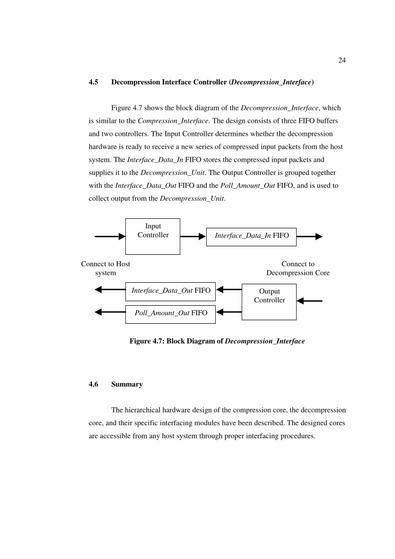
4.5 Decompression Interface Controller (Decompression_Interface)
Figure 4.7 shows the block diagram of the Decompression_Interface, which
is similar to the Compression_Interface. The design consists of three FIFO buffers
and two controllers. The Input Controller determines whether the decompression
hardware is ready to receive a new series of compressed input packets from the host
system. The Interface_Data_In FIFO stores the compressed input packets and
supplies it to the Decompression_Unit. The Output Controller is grouped together
with the Interface_Data_Out FIFO and the Poll_Amount_Out FIFO, and is used to
collect output from the Decompression_Unit.
Figure 4.7: Block Diagram of Decompression_Interface
4.6 Summary
The hierarchical hardware design of the compression core, the decompression
core, and their specific interfacing modules have been described. The designed cores
are accessible from any host system through proper interfacing procedures.
Interface_Data_In FIFO
Input
Controller
Interface_Data_Out FIFO
Poll_Amount_Out FIFO
Output
Controller
Connect to Host
system
Connect to
Decompression Core

CHAPTER V
DESIGN VERIFICATION AND PERFORMANCE ANALYSIS
This chapter reports the results obtained on testing the data compression
hardware design using the hardware evaluation system. It starts with design
verification, followed by the performance analysis.
5.1 Design Verification
In the following sub-sections, design verification results using timing
simulation and hardware test are presented. Section 5.1.1 describes the timing
simulation results and Section 5.1.2 presents the results obtained from hardware test.
Taking into account factors such as resource limitation on the FPGA device
and the 32-bit communication interface supported by the PCI device driver, the PCI-
based data compression hardware core (labeled as PCI_Chip) is configured
according to the parameters as listed in Table 5.1 for hardware implementation. The
actual hardware is the EPF10K200SFC672-1 FPGA device. This is the device
available on the Altera PCI development board. The device has 9984 logic cells
(LCs) grouped into 1248 logic array blocks (LABs) for complex logic functions, and
98304 memory bits grouped into 24 embedded array blocks (EABs) for memory
functions [Altera 1999].

26
Table 5.1: Parameter Configuration of the
PCI-based Data Compression Hardware Core
PARAMETER VALUE
SymbolWIDTH 16
DicLEVEL 7
MAXWIDTH 5
IniDicValue 0
InterfaceWIDTH 5
PollAmount 64
5.1.1 Results of Timing Simulation
For timing simulation, the design parameters are also set according to the
parameter configuration as listed in Table 5.1. Several simple source data are
encoded by the compression core. These encoded data (the compressed data) are then
decoded using the decompression core. The restored output is found to be identical to
the original source data. This timing simulation results prove that the decompression
core is able to restore the original source data, which are compressed by the
compression core.
Since timing simulation is very time-consuming, only one test vector from
the standard data set, “paper4.txt” (the benchmark data set obtained from Calgary
text compression corpus), is chosen for the timing simulation. This test vector is
successfully applied, proving correct operation of both compression and
decompression cores.
5.1.2 Results of Hardware Test
The complete compression and decompression design is further verified
through a PC-based compression hardware evaluation system. All the compression
27
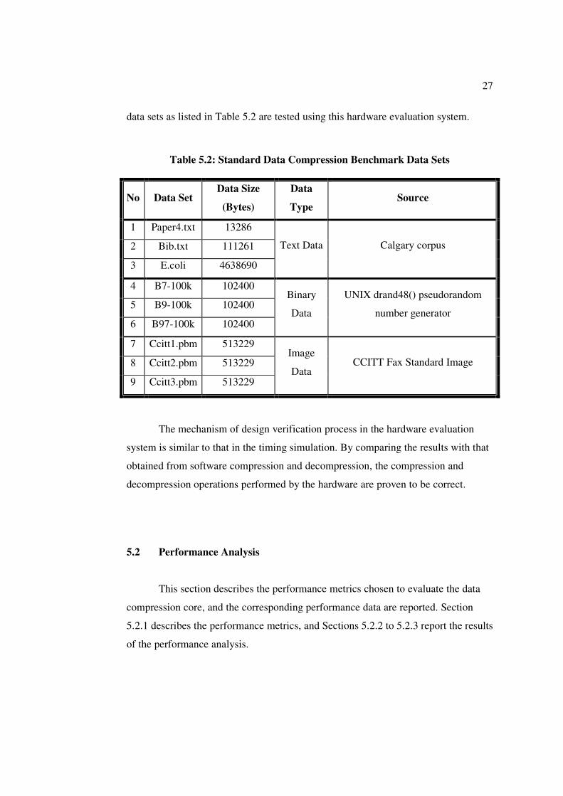
data sets as listed in Table 5.2 are tested using this hardware evaluation system.
Table 5.2: Standard Data Compression Benchmark Data Sets
No Data Set Data Size
(Bytes)
Data
Type Source
1 Paper4.txt 13286
2 Bib.txt 111261
3 E.coli 4638690
Text Data Calgary corpus
4 B7-100k 102400
5 B9-100k 102400
6 B97-100k 102400
Binary
Data
UNIX drand48() pseudorandom
number generator
7 Ccitt1.pbm 513229
8 Ccitt2.pbm 513229
9 Ccitt3.pbm 513229
Image
Data CCITT Fax Standard Image
The mechanism of design verification process in the hardware evaluation
system is similar to that in the timing simulation. By comparing the results with that
obtained from software compression and decompression, the compression and
decompression operations performed by the hardware are proven to be correct.
5.2 Performance Analysis
This section describes the performance metrics chosen to evaluate the data
compression core, and the corresponding performance data are reported. Section
5.2.1 describes the performance metrics, and Sections 5.2.2 to 5.2.3 report the results
of the performance analysis.

28
5.2.1 Performance Metrics Applied
The performance of the data compression core is analyzed using three main
performance metrics. The first metric is the area evaluation, where the amount of
logic cells (LC) and memory bits in the EPF10K200SFC672-1 device used to
implement the design is determined. It provides a measure of the required hardware
cost when fabricating the design. The second metric is compression saving, which
represents the efficiency of the compression algorithm. This is normally given as
compression ratio, and the formula used is
Compression Ratio (CR) = SCD / SSD (1)
where SCD is the size of compressed data and SSD is the size of source data. When
compressing several source data, the compression saving is measured using the
weighted average compression ratio, and the formula used is
Weighted Average CR = ���� SCD / ���� SSD (2)
The third metric is operation speed. Speed performance measures the time
required to compress source data or to restore a compressed data. It is related to
throughput, defined as
Throughput (TP) = SSD / T (3)
where T is the time to compress data or to restore the source data. The throughput
value is affected by the latency of the pipelined implementation. Tables 5.3 and 5.4
summarize the latency of our design.
Table 5.3: Latency of Compression Core
Function Pipelined Component Latency (clock cycle)
Systolic Array 1
Reduce Tree DicLEVEL LZSS Coding
Codeword Generator 1
Fixed Huffman Coding Fixed Huffman Coder 1
Pack Data Data Packer 1
Total Latency 4 + DicLEVEL

29
Table 5.4: Latency of Decompression Core
Function Pipelined Component Latency (clock cycle)
Unpack Data Data Unpacker 1
Fixed Huffman Decoding Fixed Huffman Decoder 1
Store LZSS Codeword LZSS Codeword FIFO 1
Codeword Analyzer 1
Dictionary 1 LZSS Decoding
Symbol Generator 1
Total Latency 6
Since our design processes a symbol every clock cycle, the formula for
calculating throughput is
TP = f * SymbolWIDTH (4)
where f is clock frequency and SymbolWIDTH is the length of the symbol.
From equations (3) and (4), the formula for calculating the time to compress
or decompress data is
T ≈≈≈≈ NoOfSymbol / f (5)
where NoOfSymbol = (SSD / SymbolWIDTH). Since typically the value of
NoOfSymbol >> total latency, the latency effect on throughput, and thus on time T
can be neglected.
5.2.2 Performance Analysis – Clock Speed and Area
The maximum clock speed can be obtained from the timing analyzer in
MAX+plus II. For the design configured according to the parameters listed in Table
5.1, the area and speed results are summarized in Table 5.5.

30
Table 5.5: Area and Speed Evaluation Results
Evaluation Compression
Core
Decompression
Core PCI_Chip
LE 7644 1145 9362
Area Memory
Bit 23040 26112 54528
Frequency 54.34 MHz 53.76 MHz 46.51 MHz Speed
Throughput 869.44 Mbps 860.16 Mbps 744.16 Mbps
5.2.3 Performance Analysis – Compression Ratio
In order to evaluate the compression ratio and computation time, the
hardware evaluation system is clocked at the PCI clock frequency, which is 33 MHz,
thus resulting in a throughput of 528 Mbps [calculated using equation (4)]. The
compression ratio achieved is shown in Table 5.6. A better compression ratio could
be achieved if the design is implemented in a larger device (because it can
accommodate a larger dictionary size).
The time taken to execute compression and decompression operations are
shown in Tables 5.7 and 5.8. The hardware evaluation system executes the
compression operation faster than that through software running on a 1 GHz PIII
CPU with 1 GB RDRAM. The computation time for the evaluation system is longer
than the actual compression time for the compression core calculated using equation
(5). This is because the whole operation performed by the evaluation system involves
a lot of software overhead. These software overheads include:
1. division of processor time among many tasks by the OS
2. data transfer between host PC and the PCI_Chip.

31
Table 5.6: Compression Ratio
Data Set Compression Ratio Weighted Average
Compression Ratio
Paper4.txt 0.760
Bib.txt 0.811 Text Data
E.coli 0.416
0.426
B7-100k 0.197
B9-100k 0.122 Binary Data
B97-100k 0.062
0.127
Ccitt1.pbm 0.104
Ccitt2.pbm 0.091 Image Data
Ccitt3.pbm 0.152
0.116
Table 5.7: Computation Time for Compression
Compression Time (ms)
Data Set No. of
Symbols Compression
Core (33 MHz)
PC-Based
Evaluation System
(33 MHz)
Software (1
GHz PIII
CPU)
Paper4.txt 6643 0.2 8 16
Bib.txt 55631 1.7 48 141
E.coli 2319345 70.3 2110 6140
B7-100k 51200 1.6 39 156
B9-100k 51200 1.6 39 156
B97-100k 51200 1.6 41 140
Ccitt1.pbm 256615 7.8 224 610
Ccitt2.pbm 256615 7.8 223 656
Ccitt3.pbm 256615 7.8 221 687
Total Computation
Time 100.1 2951 8702

32
Data transfer time for the PCI bus, system memory and hard disk varies
according to the mode of operation, that is whether read or write operation. Since the
size of a compressed data is smaller than the size of a source data, time for data
transfer for compression and decompression is not equal. Table 5.8 shows that the
PC-based evaluation system takes a longer time to execute decompression operation.
Table 5.8: Computation Time for Decompression
Decompression Time (ms)
Data Set No of
Symbol
Decompression
Core
(33MHz)
PC-Based Evaluation
System
(33MHz)
Software
(1GHz PIII
CPU)
Paper4.txt 6643 0.2 8 16
Bib.txt 55631 1.7 79 47
E.coli 2319345 70.3 3381 2562
B7-100k 51200 1.6 56 31
B9-100k 51200 1.6 53 32
B97-100k 51200 1.6 56 31
Ccitt1.pbm 256615 7.8 279 204
Ccitt2.pbm 256615 7.8 278 188
Ccitt3.pbm 256615 7.8 286 188
Total Computation
Time 100.1 4476 3299
5.2.4 Performance Analysis – Comparison with Other Implementations
The performance of our compression core, compared to other data
compression implementations is presented in this section. The comparisons are made
in terms of speed and compression ratio. The area comparison is not done due to
different process technology in implementing each design.

33
Table 5.9 compares the designed hardware against several popular high-
performance ASIC or FPGA lossless data compression hardware. It is found that our
data compression core offers a competitive performance to currently available ASIC
or FPGA data compression hardware. In addition, it is parameterizable to
accomodate reusability for future applications.
Table 5.9: Comparison of Data Compression Hardware Using Text Data
DEVELOPER
Technische
Universiteit
Eindhoven
[Benchop
1997]
System Design
Group
Loughborough
University
[Nunez 2000]
Universiti Teknologi
Malaysia
PROCESS
TECHNOLOGY
0.35 micron
gate array
0.25 micron
FLASH-CMOS
FPGA Actel
A500K ProASIC
EPF10K200SFC672-
1
ALGORITHM LZH X-MatchPRO LZSS + Huffman
THROUGHPUT 100 Mbps 800 Mbps 869.44 Mbps
PARAMETERIZABLE No No Yes
COMPRESSION
RATIO 0.358 0.58 0.426
5.3 Summary
The results of design verification and performance analysis are reported in
this chapter. With the results obtained from timing simulation and hardware
evaluation, the functionality of our design is proved. We also report the performance
metrics of our design, and compare the results with other data compression
implementations.
CHAPTER VI
CONCLUSIONS
This chapter summarizes the research findings, followed by suggestions for
potential future work.
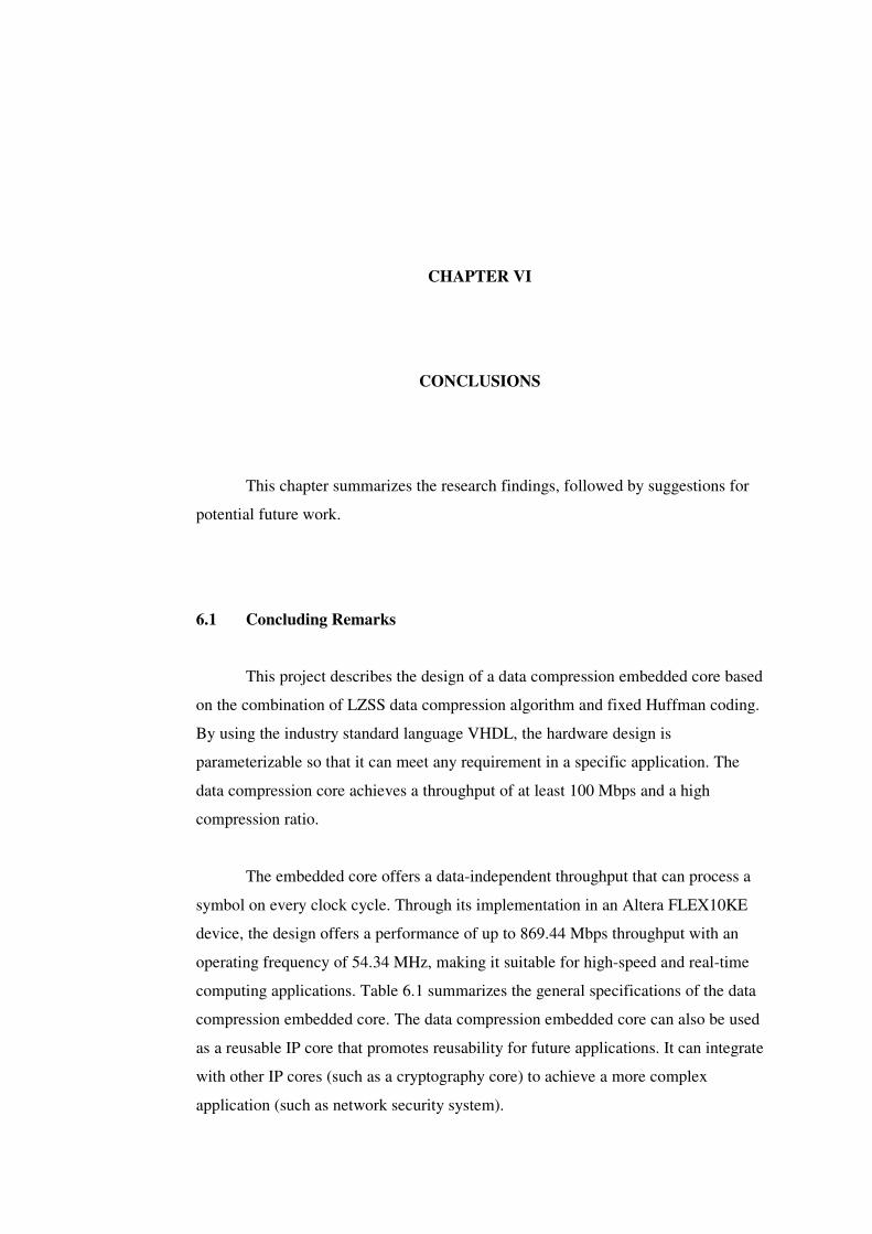
6.1 Concluding Remarks
This project describes the design of a data compression embedded core based
on the combination of LZSS data compression algorithm and fixed Huffman coding.
By using the industry standard language VHDL, the hardware design is
parameterizable so that it can meet any requirement in a specific application. The
data compression core achieves a throughput of at least 100 Mbps and a high
compression ratio.
The embedded core offers a data-independent throughput that can process a
symbol on every clock cycle. Through its implementation in an Altera FLEX10KE
device, the design offers a performance of up to 869.44 Mbps throughput with an
operating frequency of 54.34 MHz, making it suitable for high-speed and real-time
computing applications. Table 6.1 summarizes the general specifications of the data
compression embedded core. The data compression embedded core can also be used
as a reusable IP core that promotes reusability for future applications. It can integrate
with other IP cores (such as a cryptography core) to achieve a more complex
application (such as network security system).
35
Table 6.1: Specifications of the Data Compression Embedded Core
Function A real-time data compression and decompression engine
Algorithm Combination of Lempel-Ziv-Storer-Szymanski (LZSS) and
Huffman Coding
Architecture Systolic Array, Parallel, Pipelined
Feature Parameterizable - Compromise between speed, compression ratio
and resource
Other
Features
Data-independent throughput
Suitable for real-time and high-speed applications
Performance For the parameter configuration as listed in Table 5.1, a throughput
of 869.44 Mbps and a compression ratio of 0.426 is achieved
A PC-based hardware evaluation system for the data compression core was
also developed. This system integrates a host PC with the embedded core through
PCI communication bus. It has a user-friendly GUI program to facilitate the
verification of the data compression hardware core. The GUI program can be used to
evaluate the efficiency of a chosen configuration. It helps to evaluate the effect of
design parameters on the compression ratio. A customized version of the data
compression core can be generated using this GUI program.
6.2 Future Work
Further enhancements can be done based on the work in this project.
Adaptive Huffman coding can be implemented instead of the fixed Huffman
coder in the design. The adaptive Huffman coding proposed by [Vitter 1987] can
achieve a better compression saving than that of the fixed Huffman coding. A prior
knowledge of source data characteristics is not necessary in the adaptive Huffman
coding. It can estimate the source data characteristics during compression process,

36
and then modifies the code table that it currently uses to generate an adaptive
codeword that remains optimal for the current estimates.
The Wrap architecture proposed by [Gonzalez-Smith 1982, Storer 1992] is
worth studying. The resource utilization in this architecture is reduced. However, the
datapaths for this architecture are more complicated, resulting in a lower throughput.
The interface block in hardware evaluation platform can be enhanced to
suit hardware under test that has different types of I/O. This allows the PC-based
hardware evaluation system to test many other cores, not just the compression core.

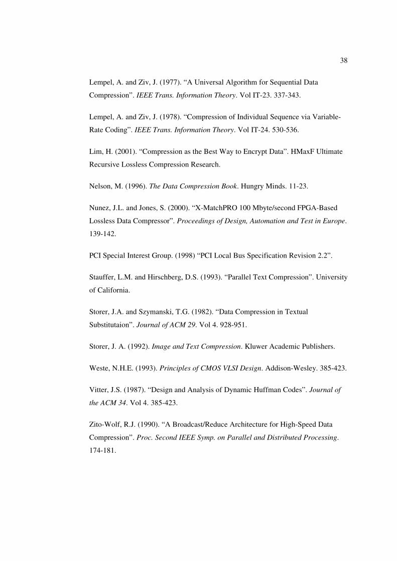
REFERENCES
Altera Corporation (1999). Altera Device Data Book. Altera Corporation.
Altera Corporation (2001). PCI MegaCore Function – User Guide. Altera
Corporation.
Benchop, L.C. (1997). “Lossless Data Compression in VLSI”. Technische
Universiteit Eindhoven: PhD’s Thesis.
Compuware Corporation (1999). “NuMega DriverAgent Help”. Compuware
Corporation.
Craft, D.J. (1995). “ALDC and a Pre-Processor Extension, BLDC, Provide Ultra Fast
Compression for General-Purpose and Bit-Mapped Image Data”. Data Compression
Conference in California. 440.
Gonzalez-Smith, M.E. and Storer, J.A. (1985). “Parallel Algorithms for Data
Compression”. Journal of the ACM. 32.
Hifn (1999). “9600 Data Compression Processor”. Hi/fn Inc.
Huang, W.J. (2000). “A Reliable LZ Data Compressor on Reconfigurable
Coprocessors”. IEEE Trans. Field-Programmable Custom Computing Machines.
249-258.
Huffman, D.A. (1952). “A Method for the Construction of Minimum Redundancy
Codes”. Proceedings IRE. Vol 40. 1098-1102.
Khalil, M. and Koay, K.H. (1999). “VHDL Module Generator: A Rapid-prototyping
Design Entry Tool for Digital ASICs”. Jurnal Teknologi 31. 45-61.
38
Lempel, A. and Ziv, J. (1977). “A Universal Algorithm for Sequential Data
Compression”. IEEE Trans. Information Theory. Vol IT-23. 337-343.
Lempel, A. and Ziv, J. (1978). “Compression of Individual Sequence via Variable-
Rate Coding”. IEEE Trans. Information Theory. Vol IT-24. 530-536.
Lim, H. (2001). “Compression as the Best Way to Encrypt Data”. HMaxF Ultimate
Recursive Lossless Compression Research.
Nelson, M. (1996). The Data Compression Book. Hungry Minds. 11-23.
Nunez, J.L. and Jones, S. (2000). “X-MatchPRO 100 Mbyte/second FPGA-Based
Lossless Data Compressor”. Proceedings of Design, Automation and Test in Europe.
139-142.
PCI Special Interest Group. (1998) “PCI Local Bus Specification Revision 2.2”.
Stauffer, L.M. and Hirschberg, D.S. (1993). “Parallel Text Compression”. University
of California.
Storer, J.A. and Szymanski, T.G. (1982). “Data Compression in Textual
Substitutaion”. Journal of ACM 29. Vol 4. 928-951.
Storer, J. A. (1992). Image and Text Compression. Kluwer Academic Publishers.
Weste, N.H.E. (1993). Principles of CMOS VLSI Design. Addison-Wesley. 385-423.
Vitter, J.S. (1987). “Design and Analysis of Dynamic Huffman Codes”. Journal of
the ACM 34. Vol 4. 385-423.
Zito-Wolf, R.J. (1990). “A Broadcast/Reduce Architecture for High-Speed Data
Compression”. Proc. Second IEEE Symp. on Parallel and Distributed Processing.
174-181.