Study of highly broadening Photonic band gaps extension in one-dimensional Metallo-organic...
17
IOSR Journal of Applied Physics (IOSR-JAP) e-ISSN: 2278-4861.Volume 5, Issue 3 (Nov. - Dec. 2013), PP 32-48 www.iosrjournals.org www.iosrjournals.org 32 | Page Study of highly broadening Photonic band gaps extension in one- dimensional Metallo-organic multilayer Photonic structure Sanjay Srivastava 1 ,Ritesh Kumar Kushwaha 2 ,K. B. Thapa 3 1 Department of Materials Science and Metallurgical Engineering, Maulana Azad National Institute of Technology, Bhoapl 462003 (M.P.) India 2 Department of Electronics and communication Engineering, Patel Institute of Technology,Bhopal 462044 (M.P.) India 3 Department of Physics,University Institute of Engineering & Technology, Chhatrapati Sahu Ji Maharaj University Kanpur -208024(U.P) India Abstract:In this paper, we show theoretically that the reflectance spectra of one dimensional multilayer metal- organic periodic structure (1D MOPS) can be enhanced due to the addition of the organic constituents. We have used simple transfer matrix method to calculate the absorption, transmittance and reflectance of the 1D MOPS systems. The organic component like N,N’-bis-(1-naphthyl)-N,N’diphenyl-1; 1biphenyl-4; 4diamine (NPB) absorbs the light in ultra-violet, visible and infrared electromagnetic region and the structure with Ag- metal also having the tendency to absorb the light by the plasmaonic action and their refractive can be calculated from Drude equation. The reflectance spectra of multilayer 1D MOPS containing a variable number periodic of Ag/N,N’-bis-(1-naphthyl)-N,N’diphenyl-1; 1biphenyl-4; 4diamine (NPB) structure are calculated taking optical constant of NPB and Ag. The optical band gap and reflectance spectra of 1D MOPS of the considered structure is obtained in the visible and near infrared regions either with the variation of the metal layer thickness or thickness of the organic layer. From the results under investigation through TMM, tunability in the optical band gap was observed either change in thickness of the other layer 1/ or 2 or the angle of the incident. Due to optical absorption of the light in the different region of electromagnetic spectrum due to either N,N’-bis-(1-naphthyl)-N,N’diphenyl-1; 1biphenyl-4; 4diamine (NPB) or silver metal, the optical band gap of 1DMOPS shows the shift of band edges of λ L and λ R from ultra-violet to visible and the infrared with change the optical constant. Keywords - Photonic crystals, Dielectric and organic layer, TE and TM mode I. Introduction Photonic band-gap material a new class of man-made material [1, 2] are a composite structure made up of periodic dielectric or metallic building blocks. Their powerful capability to control and manipulate the spectral properties of the electromagnetic waves (EM) waves leads to many novel applications in photonic devices such as frequency filters, mirrors, waveguides, frequency converters, which offers a rich ground for both theoretical and experimental research. These materials are by definition those that possess a gap in the electromagnetic wave spectrum, in which light cannot propagate in any direction. The main attraction of PBG materials is the existence of forbidden band gaps in their transmission spectra. Of the various applications on PCs, some of the important applications are optical filters, optical switches, and resonance cavities and waveguides [3, 4]. In the optical range, one-dimensional (1D) periodic structures composed of metal and dielectric layers, so-called 1D metallo-dielectric photonic crystals (MDPCs), can exhibit a high transmission band in the visible range only, blocking ultraviolet and infrared light, although the metal layer is lossy in the optical range [4-6]. As a consequence of the periodicity in the dielectric function, the speci fic wavelengths are efficiently reflected due to diffraction and interference of incident light at each interface of the periodically stacked composite. Enhanced reflectivity is achieved by increasing the number of bi -layers or by choosing dielectric materials featuring a high refractive index contrast [7]. Metallo-dielectric photonic crystals (MDPCs) can exhibit intriguing and potentially useful optical properties, including ultra-wide photonic band gaps, engineered thermal emission, and negative refractive index. They can be employed for eye protection devices, heat reflecting windows, and transparent electrodes for light- emitting diodes and liquid crystal displays [7]. One dimensional metallo-dielectric nano-films have been investigated theoretically and experimentally in the ultra-violet range [8, 9]. Zhang et al. [10] reported the optical properties of a one dimensional metallic organic photonic crystal with periodic Ag/N, N’ -bis-(1- naphthyl)-N; N’diphenyl-1; 1’biphenyl-4; 4’diamine (NPB) layers and observed the field localization within the organic layers at the resonance wavelength. Owing to resonant tunneling through the metal layers these structures combine certain properties of bulk metal with a high transparency in the desired wavelength range.
-
Upload
iosr-journals -
Category
Science
-
view
90 -
download
4
Transcript of Study of highly broadening Photonic band gaps extension in one-dimensional Metallo-organic...
IOSR Journal of Applied Physics (IOSR-JAP)
e-ISSN: 2278-4861.Volume 5, Issue 3 (Nov. - Dec. 2013), PP 32-48 www.iosrjournals.org
www.iosrjournals.org 32 | Page
Study of highly broadening Photonic band gaps extension in one-
dimensional Metallo-organic multilayer Photonic structure
Sanjay Srivastava1,Ritesh Kumar Kushwaha
2,K. B. Thapa
3
1Department of Materials Science and Metallurgical Engineering, Maulana Azad National Institute of
Technology, Bhoapl 462003 (M.P.) India 2Department of Electronics and communication Engineering, Patel Institute of Technology,Bhopal 462044
(M.P.) India 3Department of Physics,University Institute of Engineering & Technology, Chhatrapati Sahu Ji Maharaj
University
Kanpur -208024(U.P) India
Abstract:In this paper, we show theoretically that the reflectance spectra of one dimensional multilayer metal-
organic periodic structure (1D MOPS) can be enhanced due to the addition of the organic constituents. We
have used simple transfer matrix method to calculate the absorption, transmittance and reflectance of the 1D
MOPS systems. The organic component like N,N’-bis-(1-naphthyl)-N,N’diphenyl-1; 1biphenyl-4; 4diamine
(NPB) absorbs the light in ultra-violet, visible and infrared electromagnetic region and the structure with Ag-
metal also having the tendency to absorb the light by the plasmaonic action and their refractive can be calculated from Drude equation. The reflectance spectra of multilayer 1D MOPS containing a variable number
periodic of Ag/N,N’-bis-(1-naphthyl)-N,N’diphenyl-1; 1biphenyl-4; 4diamine (NPB) structure are calculated
taking optical constant of NPB and Ag. The optical band gap and reflectance spectra of 1D MOPS of the
considered structure is obtained in the visible and near infrared regions either with the variation of the metal
layer thickness or thickness of the organic layer. From the results under investigation through TMM, tunability
in the optical band gap was observed either change in thickness of the other layer 1/ or 2 or the angle of the
incident. Due to optical absorption of the light in the different region of electromagnetic spectrum due to either
N,N’-bis-(1-naphthyl)-N,N’diphenyl-1; 1biphenyl-4; 4diamine (NPB) or silver metal, the optical band gap of
1DMOPS shows the shift of band edges of λL and λR from ultra-violet to visible and the infrared with change the
optical constant.
Keywords - Photonic crystals, Dielectric and organic layer, TE and TM mode
I. Introduction Photonic band-gap material a new class of man-made material [1, 2] are a composite structure made
up of periodic dielectric or metallic building blocks. Their powerful capability to control and manipulate the
spectral properties of the electromagnetic waves (EM) waves leads to many novel applications in photonic
devices such as frequency filters, mirrors, waveguides, frequency converters, which offers a rich ground for both
theoretical and experimental research. These materials are by definition those that possess a gap in the
electromagnetic wave spectrum, in which light cannot propagate in any direction. The main attraction of PBG
materials is the existence of forbidden band gaps in their transmission spectra. Of the various applications on
PCs, some of the important applications are optical filters, optical switches, and resonance cavities and waveguides [3, 4]. In the optical range, one-dimensional (1D) periodic structures composed of metal and
dielectric layers, so-called 1D metallo-dielectric photonic crystals (MDPCs), can exhibit a high transmission
band in the visible range only, blocking ultraviolet and infrared light, although the metal layer is lossy in the
optical range [4-6]. As a consequence of the periodicity in the dielectric function, the specific wavelengths are
efficiently reflected due to diffraction and interference of incident light at each interface of the periodically
stacked composite. Enhanced reflectivity is achieved by increasing the number of bi-layers or by choosing
dielectric materials featuring a high refractive index contrast [7].
Metallo-dielectric photonic crystals (MDPCs) can exhibit intriguing and potentially useful optical
properties, including ultra-wide photonic band gaps, engineered thermal emission, and negative refractive index.
They can be employed for eye protection devices, heat reflecting windows, and transparent electrodes for light-
emitting diodes and liquid crystal displays [7]. One dimensional metallo-dielectric nano-films have been
investigated theoretically and experimentally in the ultra-violet range [8, 9]. Zhang et al. [10] reported the optical properties of a one dimensional metallic organic photonic crystal with periodic Ag/N, N’-bis-(1-
naphthyl)-N; N’diphenyl-1; 1’biphenyl-4; 4’diamine (NPB) layers and observed the field localization within the
organic layers at the resonance wavelength. Owing to resonant tunneling through the metal layers these
structures combine certain properties of bulk metal with a high transparency in the desired wavelength range.
Study of highly broadening Photonic band gaps extension in one-dimensional Metallo-organic
www.iosrjournals.org 33 | Page
The last advantage may be the most important for optical applications because it results in the tunability of both
the linear and nonlinear optical properties.
1D-PC multilayer structures of the metallic organic photonic crystal (MOPC) interacting with visible light require layer thicknesses corresponding to optical wavelengths. Actually, the structure of a transparent
metal and that of a metallodielectric photonic crystal [11] are identical, the difference being that in the case of
transparent metals the parameters are optimized for the maximum transmission. Especially, the broad
omnidirectional stop band in the metallic organic photonic crystal can inhibit light propagation in a certain
direction for a given frequency; therefore, PCs can modify significantly the emission characteristics of
embedded optically-active materials (dyes, polymers, semiconductors, etc.) as the emission wavelengths of the
active materials overlap the stop band, in the reflectance spectra of the photonic material.
The optical constant of the metal (Ag) film also depends on the wavelength which is taken from Palik
[12]. The long-range mode has an asymmetric charge distribution between the top and bottom surfaces with the
electric field predominantly normal to the surface in the metal. For thin metal films (usually less than 100 nm),
the two single-interface SPPs interact with each other and lead to two coupled SPPs, the long-range and short-range surface plasmon polariton. Conversely, the short range surface plasmon polariton (SRSPP) has a charge
distribution which is symmetric between the top and bottom surfaces with the electric field essentially parallel to
the surface.
Based on these facts, in this report, we discuss the enhanced reflectance spectra of the metallicorganic
periodic structure containing multiple layer of Ag/N,N’-bis-(1-naphthyl)-N,N’diphenyl-1; 1’biphenyl-4;
4’diamine (NPB) materials. The multiple thin layer of the various layers of periodic structure of Ag/NPB
experimentally is fabricated by dip coating technique. The thick organic layer may be deposited on the top of the
multilayer structure. TMM is used to study the reflectance spectra of the periodic structure with the air
substrates and also discussed the variation of thickness of the organic layer. The variable angle spectroscopic
ellipsometer (VASE) was used to measure the wavelength dependent optical constant of the organic film NPB
on the silver surface. The wavelength dependent optical constant of the metal (Ag) film is calculated from the
Drude relation in uv-visible region. The reflectance spectra of Ag/N, N’ bis-(1-naphthyl)-N, N’diphenyl-1; 1’biphenyl-4; 4’diamine (NPB) of multiple layer of the periodic structure is calculated by choosing proper
thickness of Ag/PNB layers and with a variation of the thickness of the organic layer NPB.
II. Formulation As for the metal layer, the usual Drude model will be employed. The temporal part of any field is
assumed to be eitω. Then the permittivity of the metal in Drude model takes the form
2
2 2( ) 1
p
j
(1)
Where ωp is the plasma frequency and γ is the damping frequency. The index of refraction of a metal is thus
given by n2 =√ε2. For obliquely incident of an electromagnetic wave on the most left boundary of organic/metal at an angle of incidence θ0, the reflectance can then be calculated by making use of the Abeles theory [13-14].
A 1D PC is composed of two different media, A and B, alternating in layers with dielectric constant "a and "b
and thickness a and b; the lattice constant d = a + b, and the number of periods is N. The photonic band structure
of a perfect photonic crystal is determined by the Eigenvalues of the following familiar equation [1]:
2
1( , ) ( )r H r H rc
(2)
Where ,r
is the dielectric constant of the crystal and ( )H r
is the monochromatic component (of
frequency v) of the magnetic field, which satisfies the Bloch condition [1]
( ) ( )bik r
kbH r e H r
(3)
bk
is the Bloch vector lying in the first Brillouin zone of the crystal’s reciprocal space ,bk
H r
and has the
same periodicity as the underlying Bravais lattice. In considering the Eigenvalue problem for the frequency ω,
Eq. (1) has a nonlinear character because the dielectric constant ,r
, which acts as a scattering potential, it
depends on the Eigenvalue ω. In terms of the electric fields, the solution of the differential Equation is
Study of highly broadening Photonic band gaps extension in one-dimensional Metallo-organic
www.iosrjournals.org 34 | Page
( / )
i t yE E x e
Where E (x/ω) can be taken as the superposition of the incident and reflected wave in
each medium, for jth layer can be written in the form
( / ) jx jxik x ik x
jE x A e Bje
(4)
Where cosjx j jkc
and εj are the wave vector and dielectric constant in the jth layer respectively, and
c is the speed of light in vacuum. The coefficients Aj and Bj have to be determined from the boundary condition
that both electric field and its first derivative are continuous across an interface. The magnetic field vector along
y-axis can be obtained by:
i
H E
(5)
Consider for the dielectric layer with no external current source and induced charge, the Maxwell equation
becomes:
. 0E
. 0B
B
Et
And D
Bt
(6)
By using the Snell’s law in the above equation, the dielectric constant of the given materials is given by the
following expression
22
2dkc
Or
2 2 22 2 2
2 2 2sin 1 sindxk
c c c
or
dx dk nc
(7)
Where the refractive index of the taken system is given by
2sindn
(8)
According to this theory, the transfer matrix methods are used to set the corresponding matrix of one period,
which is given by the following expression:
3 32 21,1 1,2
32
2,1 2,2
2 2 2 3 3 3
cos coscos cos
sin cos sin cos
jjm m
ppMm m
jp jp
32 3 2 3 2 3 2 3
2 3 2
32 2 3 3 2 3 2 3 2 3
2
cos cos sin sin cos sin sin cos
sin cos cos sin cos cos sin sin
p j j
p p pM
pjp jp
p
(9)
Where 2 2
0
2cossn d
and
3 3
0
2cosdn t
,
02 2
0
cossp n
, 0
3 3
0
cosdp n
for TE
mode and for TM-mode 0
2 2
0
1cos
s
pn
,
03 3
0
1cos
d
pn
and
0
0
2 2 c
k
is the
wavelength in free space. The angle θ1 and θ2 determined by the Snell’s law of refraction are the ray angle in
layer2 and 3 respectively. By using the above matrix, we try to construct the matrix for n-periods,
11 1 2 12 1
21 1 22 1 2
( ) ( ) ( )( ) [ ]
( ) ( ) ( )
N N NN
N N N
m U U m UM N M
m U m U U
(10) Where 11 22
1( )
2m m and UN are the Chebyshev polynomials of the second kind defined by
Study of highly broadening Photonic band gaps extension in one-dimensional Metallo-organic
www.iosrjournals.org 35 | Page
1
2
sin[( 1)cos ]( )
1N
NU
(11)
By using the above relation, the matrix elements are given by the following formula;
311 2 3 2 3 1 2
2
(cos cos sin sin ) ( ) ( )N N
pM U U
p
12 2 3 2 3 1
3 2
1 1( cos sin sin cos ) ( )NM j U
p p
12 2 2 3 3 2 3 1( sin cos cos sin ) ( )NM j p p U
211 2 3 2 3 1 2
3
(cos cos sin sin ) ( ) ( )N N
pM U U
p
(12)
The reflection and transmittance of the multilayered structure can be determined from the above Eq (12) and given
as fellows
11 12 0 21 22
11 12 0 21 22
( ) ( )
( ) ( )
s s
s s
M M p p M M pr
M M p p M M p
And 0
11 12 0 21 22
2
( ) ( )s s
pt
M M p p M M p
(13)
Here p0 and ps are the first and the last medium of the considered structure and given by, 00 0 0
0
cosp n
0
0
coss s sp n
and for TE-mode and for TM-mode0
0 0
0 0
1cosp
n
,
0
0
1coss s
s
pn
. Both
the media are taken to be a free space. The reflectivity and transmittance are given by 2
R r and 2
0
spT t
p .
III. Results And Discussion The theoretical reflectance spectra of the multilayer structure were calculated by solving the Maxwell
equations and the optical constants of Ag was calculated from the Drude model and the linear refractive index
of the N,N’-bis-(1-naphthyl)-N,N’diphenyl-1; 1’biphenyl-4; 4’diamine film was measured using an ellipsometer
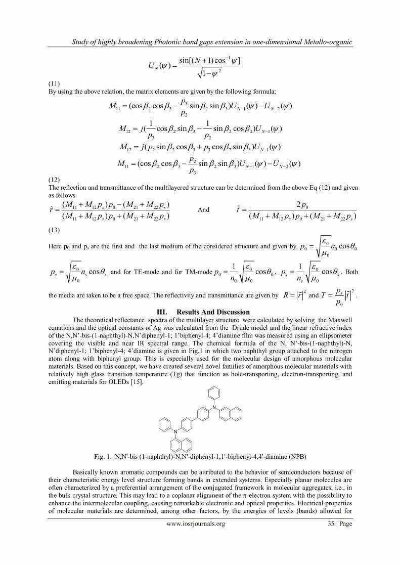
covering the visible and near IR spectral range. The chemical formula of the N, N’-bis-(1-naphthyl)-N, N’diphenyl-1; 1’biphenyl-4; 4’diamine is given in Fig.1 in which two naphthyl group attached to the nitrogen
atom along with biphenyl group. This is especially used for the molecular design of amorphous molecular
materials. Based on this concept, we have created several novel families of amorphous molecular materials with
relatively high glass transition temperature (Tg) that function as hole-transporting, electron-transporting, and
emitting materials for OLEDs [15].
N
N
Fig. 1. N,N'-bis (1-naphthyl)-N,N'-diphenyl-1,1'-biphenyl-4,4'-diamine (NPB)
Basically known aromatic compounds can be attributed to the behavior of semiconductors because of
their characteristic energy level structure forming bands in extended systems. Especially planar molecules are
often characterized by a preferential arrangement of the conjugated framework in molecular aggregates, i.e., in
the bulk crystal structure. This may lead to a coplanar alignment of the π-electron system with the possibility to
enhance the intermolecular coupling, causing remarkable electronic and optical properties. Electrical properties
of molecular materials are determined, among other factors, by the energies of levels (bands) allowed for
Study of highly broadening Photonic band gaps extension in one-dimensional Metallo-organic
www.iosrjournals.org 36 | Page
electrons and holes in these materials. The electrical energy gap molecular materials is then the difference of the
two latter parameters, being a measure of the energy difference between the energies of levels allowed for non-
interacting electrons and holes. Molecular organic materials like N,N’-bis-(1-naphthyl)-N,N’diphenyl-1; 1’biphenyl-4; 4’diamine function as holes transporting between HOMO and LUMO, electron-transporting, or
emitting materials, mainly depending upon their ionization potentials and electron affinities. HOMO and LUMO
are also called the frontier orbital’s, and their deference in energy ELUMO − EHOMO = Egap is sometimes called an
electronic band gap, although strictly speaking, bands do not occur until a spatially extended solid is formed.
The majority of typical non-substituted low-molecular weight materials like acenes, phenylenes, thiophenes,
phthalocyanines, behaves like as p-type semiconducting (hole-conducting) materials. A similar situation is
encountered in π-conjugated polymers: most of them are n-type semiconductors built of electron-releasing
macromolecules consisting of electron-rich subunits (like thiophene or pyrrole). That will provide the excess
electron density in the conduction band. Stable materials with electron accepting properties (n-type materials)
are required in all important electronic and opto-electronic applications: such as bipolar transistors, photovoltaic
devices, LEDs and FETs. Generally, organic materials having low ionization energy together with low electron affinities usually
function as hole-transporting materials by accepting holes carriers with a positive charge and transporting them
depends upon the concentration of the dopant in the matrix , while materials having high electron affinities
together with high ionization potentials usually function as electron-transporting materials by accepting negative
charges and allowing them to move through the molecules between the π-electron in the aromatic ring. Other
reasons for its popularity is because sublimed NPB can be manufactured readily and is thus abundantly
available even through its Tg at 98oC is a trifle low which may affect its morphological stability at high
operating temperature. The materials should possess high hole drift mobility to be capable of swiftly
transporting the hole through them. The following approaches used to design the complex organic molecules
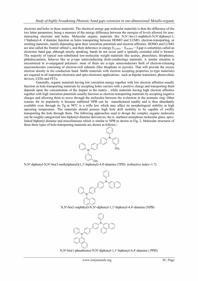
can be roughly categorized into biphenyl diamine derivatives; the π- starburst amorphous molecular glass; spiro-
linked biphenyl diamine and miscellaneous which is similar to NPB as shown in Fig. 2. Molecular structures of
these three types of hole-transporting materials are shown as follows:-
N
CH3
N
CH3
N,N'-diphenyl-N,N'-bis(3-methylphenyl)(1,1'-biphenyl)-4,4'-diamine (TPD) (refractive index=1.7)
N
N
N,N'-bis(1-naphthyl)-N,N'-diphenyl-1,1'-biphenyl-4,4'-diamine (NPB)
N
N
N,N'-bis(1-phnathrene)-N,N'-diphenyl-1,1'-biphenyl-4,4'-diamine ( PPD)
Study of highly broadening Photonic band gaps extension in one-dimensional Metallo-organic
www.iosrjournals.org 37 | Page
N
N
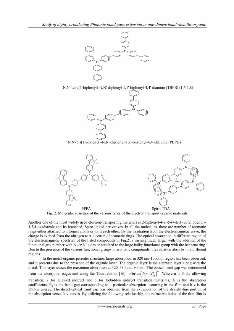
N,N'-tetra(1-biphenyl)-N,N'-diphenyl-1,1'-biphenyl-4,4'-diamine (TBPB) (1.6-1.8)
N
N
N,N'-bis(1-biphenyl)-N,N'-diphenyl-1,1'-biphenyl-4,4'-diamine (PBPD)
N
N
N
N
N
N
PFFA Spiro-TDA
Fig. 2. Molecular structure of the various types of the electron transport organic materials
Another one of the most widely used electron-transporting materials is 2-biphenyl-4-yl-5-(4-tert -butyl phenyl)-
1,3,4-oxadiazole and its branched, Spiro-linked derivatives. In all the molecules, there are number of aromatic
rings either attached to nitrogen atoms or joint each other. By the irradiation from the electromagnetic wave, the
charge is excited from the nitrogen to π-electron of aromatic rings. The optical absorption in different region of the electromagnetic spectrum of the listed compounds in Fig.2 is varying much larger with the addition of the
functional group either with N /or N’ sides or attached to the large bulky functional group with the benzene ring.
Due to the presence of the various functional groups in aromatic compounds, the radiation absorbs in a different
regions.
In the metal-organic periodic structure, large absorption in 320 nm-1000nm region has been observed,
and it presents due to the presence of the organic layer. The organic layer is the alternate layer along with the
metal. This layer shows the maximum absorption at 320, 380 and 800nm. The optical band gap was determined
from the absorption edges and using the Tauc-relation [16]: n
gAh h E . Where n is ½ for allowing
transition, 2 for allowed indirect and 3 for forbidden indirect transition materials, A is the absorption
coefficients, Eg is the band gap corresponding to a particular absorption occurring in the film and h ν is the
photon energy. The direct optical band gap was obtained from the extrapolation of the straight-line portion of
the absorption versus h ν curves. By utilizing the following relationship, the refractive index of the thin film is
Study of highly broadening Photonic band gaps extension in one-dimensional Metallo-organic
www.iosrjournals.org 38 | Page
directly calculated:
2
2
11
2 20
gEn
n
.However, metals are not optically transparent and the dielectric
constant is a complex quantity and a function of frequency. The metallic layer is taken to be silver (Ag) with the
plasma frequency ωp is defined by
22
0
p
eff
Ne
m
= 2πx2.175x1015 rad/s and the damping frequency is γ°
=2πx4.35x1012 rad/s [17] where N is the electron density, meff is the effective mass of the electron, e is the electronic charge and the permittivity of the vacuum is ε0. It is clear that changing N will cause the plasma
frequency to be changed, which, in turn, leads to a variation in the permittivity of a plasma system. The real part
of the permittivity is negative and describes the dielectric properties. The positive imaginary part defines the
intrinsic material absorption which leads to an evanescent mode of propagating electromagnetic (EM) wave
incident on the surface the metal from a dielectric medium. With a variable permittivity, a plasma system can be
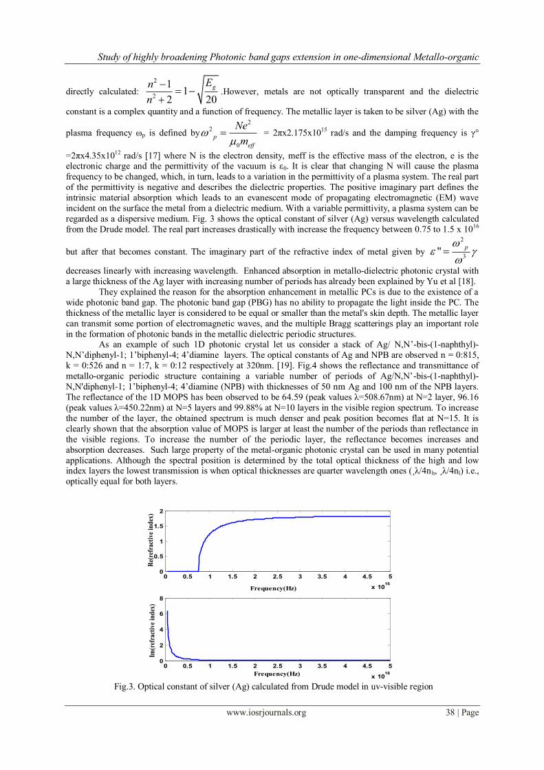
regarded as a dispersive medium. Fig. 3 shows the optical constant of silver (Ag) versus wavelength calculated
from the Drude model. The real part increases drastically with increase the frequency between 0.75 to 1.5 x 10¹⁶
but after that becomes constant. The imaginary part of the refractive index of metal given by
2
3"
p
decreases linearly with increasing wavelength. Enhanced absorption in metallo-dielectric photonic crystal with
a large thickness of the Ag layer with increasing number of periods has already been explained by Yu et al [18].
They explained the reason for the absorption enhancement in metallic PCs is due to the existence of a
wide photonic band gap. The photonic band gap (PBG) has no ability to propagate the light inside the PC. The
thickness of the metallic layer is considered to be equal or smaller than the metal's skin depth. The metallic layer
can transmit some portion of electromagnetic waves, and the multiple Bragg scatterings play an important role
in the formation of photonic bands in the metallic dielectric periodic structures. As an example of such 1D photonic crystal let us consider a stack of Ag/ N,N’-bis-(1-naphthyl)-
N,N’diphenyl-1; 1’biphenyl-4; 4’diamine layers. The optical constants of Ag and NPB are observed n = 0:815,
k = 0:526 and n = 1:7, k = 0:12 respectively at 320nm. [19]. Fig.4 shows the reflectance and transmittance of
metallo-organic periodic structure containing a variable number of periods of Ag/N,N’-bis-(1-naphthyl)-
N,N'diphenyl-1; 1’biphenyl-4; 4’diamine (NPB) with thicknesses of 50 nm Ag and 100 nm of the NPB layers.
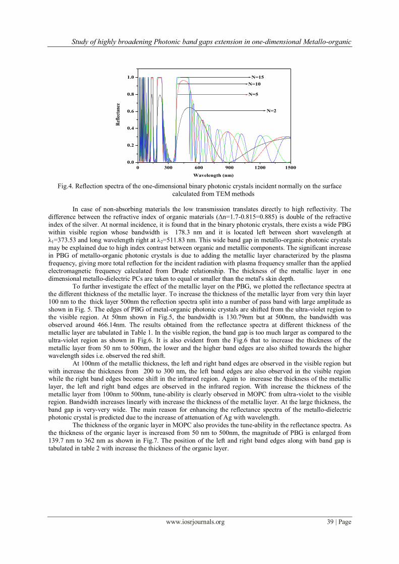
The reflectance of the 1D MOPS has been observed to be 64.59 (peak values λ=508.67nm) at N=2 layer, 96.16
(peak values λ=450.22nm) at N=5 layers and 99.88% at N=10 layers in the visible region spectrum. To increase
the number of the layer, the obtained spectrum is much denser and peak position becomes flat at N=15. It is
clearly shown that the absorption value of MOPS is larger at least the number of the periods than reflectance in
the visible regions. To increase the number of the periodic layer, the reflectance becomes increases and
absorption decreases. Such large property of the metal-organic photonic crystal can be used in many potential
applications. Although the spectral position is determined by the total optical thickness of the high and low index layers the lowest transmission is when optical thicknesses are quarter wavelength ones (¸λ/4nh, ¸λ/4nl) i.e.,
optically equal for both layers.
Fig.3. Optical constant of silver (Ag) calculated from Drude model in uv-visible region
0 0.5 1 1.5 2 2.5 3 3.5 4 4.5 5
x 1016
0
0.5
1
1.5
2
0 0.5 1 1.5 2 2.5 3 3.5 4 4.5 5
x 1016
0
2
4
6
8
Frequency(Hz)
Im(r
efra
ctiv
e in
dex
)R
e(re
frac
tive
in
dex
)
Frequency(Hz)
Study of highly broadening Photonic band gaps extension in one-dimensional Metallo-organic
www.iosrjournals.org 39 | Page
0 300 600 900 1200 1500
0.0
0.2
0.4
0.6
0.8
1.0
N=5
N=10
N=15
N=2
Ref
lect
ance
Wavelength (nm)
Fig.4. Reflection spectra of the one-dimensional binary photonic crystals incident normally on the surface
calculated from TEM methods
In case of non-absorbing materials the low transmission translates directly to high reflectivity. The
difference between the refractive index of organic materials (Δn=1.7-0.815=0.885) is double of the refractive
index of the silver. At normal incidence, it is found that in the binary photonic crystals, there exists a wide PBG
within visible region whose bandwidth is 178.3 nm and it is located left between short wavelength at
λ1=373.53 and long wavelength right at λ2=511.83 nm. This wide band gap in metallo-organic photonic crystals
may be explained due to high index contrast between organic and metallic components. The significant increase
in PBG of metallo-organic photonic crystals is due to adding the metallic layer characterized by the plasma
frequency, giving more total reflection for the incident radiation with plasma frequency smaller than the applied
electromagnetic frequency calculated from Drude relationship. The thickness of the metallic layer in one
dimensional metallo-dielectric PCs are taken to equal or smaller than the metal's skin depth.
To further investigate the effect of the metallic layer on the PBG, we plotted the reflectance spectra at the different thickness of the metallic layer. To increase the thickness of the metallic layer from very thin layer
100 nm to the thick layer 500nm the reflection spectra split into a number of pass band with large amplitude as
shown in Fig. 5. The edges of PBG of metal-organic photonic crystals are shifted from the ultra-violet region to
the visible region. At 50nm shown in Fig.5, the bandwidth is 130.79nm but at 500nm, the bandwidth was
observed around 466.14nm. The results obtained from the reflectance spectra at different thickness of the
metallic layer are tabulated in Table 1. In the visible region, the band gap is too much larger as compared to the
ultra-violet region as shown in Fig.6. It is also evident from the Fig.6 that to increase the thickness of the
metallic layer from 50 nm to 500nm, the lower and the higher band edges are also shifted towards the higher
wavelength sides i.e. observed the red shift.
At 100nm of the metallic thickness, the left and right band edges are observed in the visible region but
with increase the thickness from 200 to 300 nm, the left band edges are also observed in the visible region while the right band edges become shift in the infrared region. Again to increase the thickness of the metallic
layer, the left and right band edges are observed in the infrared region. With increase the thickness of the
metallic layer from 100nm to 500nm, tune-ability is clearly observed in MOPC from ultra-violet to the visible
region. Bandwidth increases linearly with increase the thickness of the metallic layer. At the large thickness, the
band gap is very-very wide. The main reason for enhancing the reflectance spectra of the metallo-dielectric
photonic crystal is predicted due to the increase of attenuation of Ag with wavelength.
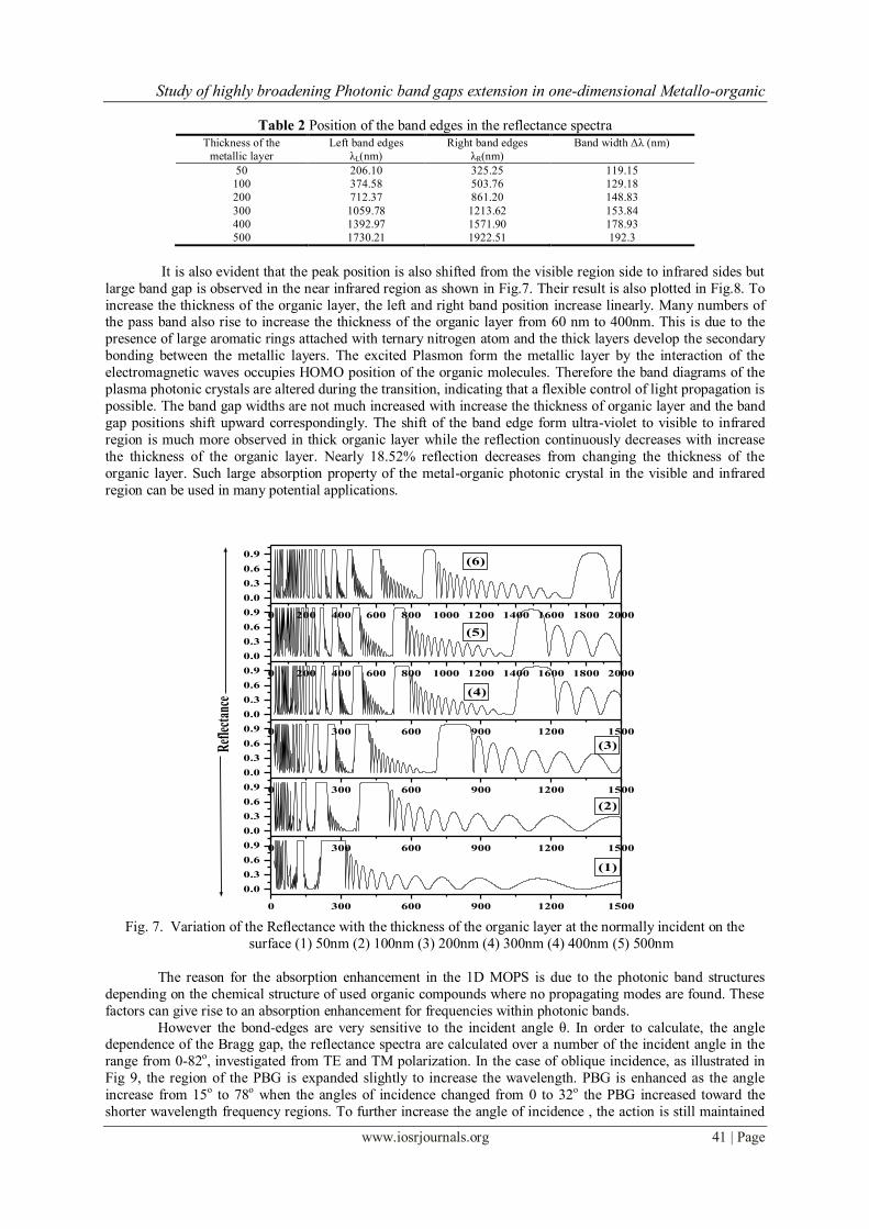
The thickness of the organic layer in MOPC also provides the tune-ability in the reflectance spectra. As
the thickness of the organic layer is increased from 50 nm to 500nm, the magnitude of PBG is enlarged from
139.7 nm to 362 nm as shown in Fig.7. The position of the left and right band edges along with band gap is
tabulated in table 2 with increase the thickness of the organic layer.
Study of highly broadening Photonic band gaps extension in one-dimensional Metallo-organic
www.iosrjournals.org 40 | Page
0 300 600 900 1200 1500
0.0
0.3
0.6
0.9
0.0
0.3
0.6
0.9
0.0
0.3
0.6
0.9
0.0
0.3
0.6
0.9
0.0
0.3
0.6
0.9
0.0
0.3
0.6
0.9
Wavelength(nm)
Ref
lect
ance
(6)
(5)
(4)
(3)
(2)
(1)
Fig. 5. Reflection spectra of the one-dimensional binary photonic crystals incident normally on the surface
versus wavelength at the different thickness of the metallic layer (1) 50nm (2) 100nm (3) 200nm (4) 300nm
(5) 400nm (6) 500nm
Table 1. Position of the band edges in the reflectance spectra with the variation of the metallic layer thickness
(the refractive index of the organic layer n2=1.7) Thickness of the
metallic layer
Left band edges
λL(nm)
Right band edges
λR(nm)
Band width Δλ (nm)
50 373.54 505.33 130.79
100 423.33 647.58 224.25
200 533.44 871.23 337.79
300 682.27 1079.43 397.16
400 831.52 1267.97 436.45
500 985.36 1457.50 472.14
0 100 200 300 400 500
300
450
600
750
900
1050
1200
1350
1500
Wavelength (nm)
Po
isti
on
of
the b
an
d e
dg
e (
nm
)
100
150
200
250
300
350
400
450
500
R
L
Ba
nd
wid
th(n
m)
Fig. 6 Variation of the band width with the thickness of the metallic layer at the normally incident on the surface
Study of highly broadening Photonic band gaps extension in one-dimensional Metallo-organic
www.iosrjournals.org 41 | Page
Table 2 Position of the band edges in the reflectance spectra Thickness of the
metallic layer
Left band edges
λL(nm)
Right band edges
λR(nm)
Band width Δλ (nm)
50 206.10 325.25 119.15
100 374.58 503.76 129.18
200 712.37 861.20 148.83
300 1059.78 1213.62 153.84
400 1392.97 1571.90 178.93
500 1730.21 1922.51 192.3
It is also evident that the peak position is also shifted from the visible region side to infrared sides but
large band gap is observed in the near infrared region as shown in Fig.7. Their result is also plotted in Fig.8. To
increase the thickness of the organic layer, the left and right band position increase linearly. Many numbers of the pass band also rise to increase the thickness of the organic layer from 60 nm to 400nm. This is due to the
presence of large aromatic rings attached with ternary nitrogen atom and the thick layers develop the secondary
bonding between the metallic layers. The excited Plasmon form the metallic layer by the interaction of the
electromagnetic waves occupies HOMO position of the organic molecules. Therefore the band diagrams of the
plasma photonic crystals are altered during the transition, indicating that a flexible control of light propagation is
possible. The band gap widths are not much increased with increase the thickness of organic layer and the band
gap positions shift upward correspondingly. The shift of the band edge form ultra-violet to visible to infrared
region is much more observed in thick organic layer while the reflection continuously decreases with increase
the thickness of the organic layer. Nearly 18.52% reflection decreases from changing the thickness of the
organic layer. Such large absorption property of the metal-organic photonic crystal in the visible and infrared
region can be used in many potential applications.
0 300 600 900 1200 1500
0.0
0.3
0.6
0.9 0 300 600 900 1200 1500
0.0
0.3
0.6
0.9 0 300 600 900 1200 1500
0.0
0.3
0.6
0.9 0 300 600 900 1200 1500
0.0
0.3
0.6
0.9 0 200 400 600 800 1000 1200 1400 1600 1800 2000
0.0
0.3
0.6
0.9 0 200 400 600 800 1000 1200 1400 1600 1800 2000
0.0
0.3
0.6
0.9(6)
(5)
(3)
(2)
(4)
Wavelength (nm)
(1)
Ref
lect
ance
Fig. 7. Variation of the Reflectance with the thickness of the organic layer at the normally incident on the
surface (1) 50nm (2) 100nm (3) 200nm (4) 300nm (4) 400nm (5) 500nm
The reason for the absorption enhancement in the 1D MOPS is due to the photonic band structures
depending on the chemical structure of used organic compounds where no propagating modes are found. These
factors can give rise to an absorption enhancement for frequencies within photonic bands.
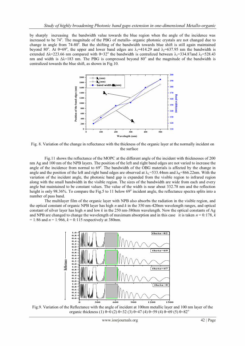
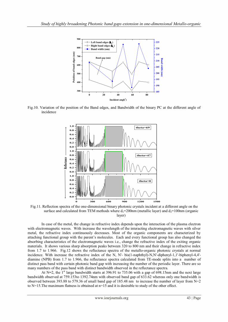
However the bond-edges are very sensitive to the incident angle θ. In order to calculate, the angle dependence of the Bragg gap, the reflectance spectra are calculated over a number of the incident angle in the
range from 0-82o, investigated from TE and TM polarization. In the case of oblique incidence, as illustrated in
Fig 9, the region of the PBG is expanded slightly to increase the wavelength. PBG is enhanced as the angle
increase from 15o to 78o when the angles of incidence changed from 0 to 32o the PBG increased toward the
shorter wavelength frequency regions. To further increase the angle of incidence , the action is still maintained
Study of highly broadening Photonic band gaps extension in one-dimensional Metallo-organic
www.iosrjournals.org 42 | Page
by sharply increasing the bandwidth value towards the blue region when the angle of the incidence was
increased to be 74o. The magnitude of the PBG of metallo- organic photonic crystals are not changed due to
change in angle from 74-80o. But the shifting of the bandwidth towards blue shift is still again maintained beyond 80o. At θ=69o, the upper and lower band edges are λ1=414.29 and λ2=637.95 nm the bandwidth is
extended Δλ=223.66 nm compared with θ=32o the bandwidth is centralized between λ1=334.87and λ2=528.43
nm and width is Δλ=183 nm. The PBG is compressed beyond 80o and the magnitude of the bandwidth is
centralized towards the blue shift, as shown in Fig.10.
0 100 200 300 400 500
0
200
400
600
800
1000
1200
1400
1600
1800
2000
R
L
L(nm)
R(nm)
band width (nm)
Wavelngth (nm)
Po
siti
on
of
the
ba
nd
ed
ges
(n
m)
110
120
130
140
150
160
170
180
190
200
Ba
nd
wid
th(n
m)
Fig. 8. Variation of the change in reflectance with the thickness of the organic layer at the normally incident on
the surface
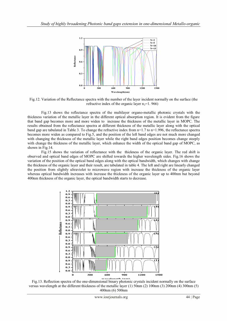
Fig.11 shows the reflectance of the MOPC at the different angle of the incident with thicknesses of 200
nm Ag and 100 nm of the NPB layers. The position of the left and right band edges are not varied to increase the
angle of the incidence from normal to 69o. The bandwidth of the OBG materials is affected by the change in
angle and the position of the left and right band edges are observed at λL=533.44nm and λR=866.22nm. With the
variation of the incident angle, the photonic band gap is expanded from the visible region to infrared region
along with the small bandwidth in the visible region. The sizes of the bandwidth are wide from each and every angle but maintained to be constant values. The value of the width is near about 332.78 nm and the reflection
height is only 98.36%. To compare the Fig.5 to 11 below 69o incident angle, the reflectance spectra splits into a
number of pass band.
The multilayer film of the organic layer with NPB also absorbs the radiation in the visible region, and
the optical constant of organic NPB layer has high n and k in the 350 nm-420nm wavelength ranges, and optical
constant of silver layer has high n and low k in the 250 nm-380nm wavelength. Now the optical constants of Ag
and NPB are changed to change the wavelength of maximum absorption and in this case it is taken n = 0:178, k
= 1:86 and n = 1:966, k = 0:115 respectively at 380nm.
0 300 600 900 1200 1500
0.0
0.2
0.4
0.6
0.8
1.0
0.0
0.2
0.4
0.6
0.8
1.0
0.0
0.2
0.4
0.6
0.8
1.0
0.0
0.2
0.4
0.6
0.8
1.0
Wavelength
theta=0
Refle
ctanc
e
theta=47
theta=69
theta=82
Fig.9. Variation of the Reflectance with the angle of incident at 100nm metallic layer and 100 nm layer of the
organic thickness (1) θ=0 (2) θ=32 (3) θ=47 (4) θ=59 (4) θ=69 (5) θ=82o
Study of highly broadening Photonic band gaps extension in one-dimensional Metallo-organic
www.iosrjournals.org 43 | Page
0 20 40 60 80
300
400
500
600
700
800
900
Left band edges (L)
Right band edges (L)
Band width (nm)
Incident angl(o)
Po
isit
ion
of
ba
nd
ed
ges
(n
m)
185
190
195
200
205
210
215
220
225
Band gap (nm) Ba
nd
wid
th (n
m)
Fig.10. Variation of the position of the Band edges, and Bandwidth of the binary PC at the different angle of
incidence
0 300 600 900 1200 1500
0.0
0.2
0.4
0.6
0.8
1.0
0.0
0.2
0.4
0.6
0.8
1.0
0.0
0.2
0.4
0.6
0.8
1.0
Wavelength (nm)
theta=0
Ref
lect
ance
theta=47
theta=69
Fig.11. Reflection spectra of the one-dimensional binary photonic crystals incident at a different angle on the
surface and calculated from TEM methods where d1=200nm (metallic layer) and d2=100nm (organic
layer)
In case of the metal, the change in refractive index depends upon the interaction of the plasma electron
with electromagnetic waves. With increase the wavelength of the interacting electromagnetic waves with silver
metal, the refractive index continuously decreases. Most of the organic components are characterized by
attaching functional group with the parent’s molecules. Each and every functional group has also changed the
absorbing characteristics of the electromagnetic waves i.e., change the refractive index of the exiting organic
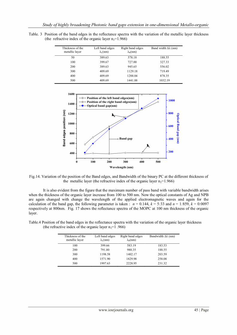
materials. It shows various sharp absorption peaks between 320 to 800 nm and their change in refractive index
from 1.7 to 1.966. Fig.12 shows the reflectance spectra of the metallo-organic photonic crystals at normal
incidence. With increase the refractive index of the N, N'- bis(1-naphthyl)-N,N'-diphenyl-1,1'-biphenyl-4,4'-
diamine (NPB) from 1.7 to 1.966, the reflectance spectra calculated from TE-mode splits into a number of
distinct pass band with certain photonic band gap with increasing the number of the periodic layer. There are so many numbers of the pass band with distinct bandwidth observed in the reflectance spectra.
At N=2, the 1st large bandwidth starts at 396.91 to 735.06 with a gap of 698.15nm and the next large
bandwidth observed at 759.153to 1392.74nm with observed band gap of 633.62 whereas only one bandwidth is
observed between 393.88 to 579.36 of small band gap of 185.48 nm to increase the number of layer from N=2
to N=15.The maximum flatness is obtained at n=15 and it is desirable to study of the other effect.
Study of highly broadening Photonic band gaps extension in one-dimensional Metallo-organic
www.iosrjournals.org 44 | Page
0 300 600 900 1200 1500
0.0
0.3
0.6
0.9
1.2
Ref
lect
an
ce
Wavelength(nm)
N=2
N=5
N=10
N=15
Fig.12. Variation of the Reflectance spectra with the number of the layer incident normally on the surface (the
refractive index of the organic layer n2=1. 966)
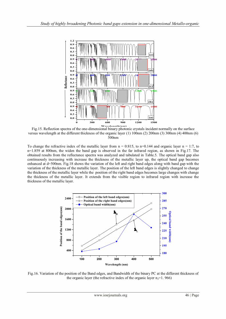
Fig.13 shows the reflectance spectra of the multilayer organo-metallic photonic crystals with the
thickness variation of the metallic layer in the different optical absorption region. It is evident from the figure
that band gap becomes more and more widen to increase the thickness of the metallic layer in MOPC. The results obtained from the reflectance spectra at different thickness of the metallic layer along with the optical
band gap are tabulated in Table 3. To change the refractive index from n=1.7 to n=1.996, the reflectance spectra
becomes more widen as compared to Fig.5, and the position of the left band edges are not much more changed
with changing the thickness of the metallic layer while the right band edges position becomes change steeply
with change the thickness of the metallic layer, which enhance the width of the optical band gap of MOPC, as
shown in Fig.14.
Fig.15 shows the variation of reflectance with the thickness of the organic layer. The red shift is
observed and optical band edges of MOPC are shifted towards the higher wavelength sides. Fig.16 shows the
variation of the position of the optical band edges along with the optical bandwidth, which changes with change
the thickness of the organic layer and their result, are tabulated in table 4. The left and right are linearly changed
the position from slightly ultraviolet to microwave region with increase the thickness of the organic layer whereas optical bandwidth increases with increase the thickness of the organic layer up to 400nm but beyond
400nm thickness of the organic layer, the optical bandwidth starts to decrease.
0 300 600 900 1200 1500
0.0
0.3
0.6
0.9
0.0
0.3
0.6
0.9
0.0
0.3
0.6
0.9
0.0
0.3
0.6
0.9
0.0
0.3
0.6
0.9
0.0
0.3
0.6
0.9
1.2
wavelength (nm)
(6)
(5)
(4)
(3)
(2)
(1)
Ref
lect
ance
Fig.13. Reflection spectra of the one-dimensional binary photonic crystals incident normally on the surface
versus wavelength at the different thickness of the metallic layer (1) 50nm (2) 100nm (3) 200nm (4) 300nm (5)
400nm (6) 500nm
Study of highly broadening Photonic band gaps extension in one-dimensional Metallo-organic
www.iosrjournals.org 45 | Page
Table. 3 Position of the band edges in the reflectance spectra with the variation of the metallic layer thickness
(the refractive index of the organic layer n2=1.966)
Thickness of the
metallic layer
Left band edges
λL(nm)
Right band edges
λR(nm)
Band width Δλ (nm)
50 389.63 578.18 188.55
100 399.67 727.00 327.33
200 389.63 945.65 556.02
300 409.69 1129.18 719.49
400 409.69 1288.04 878.35
500 409.69 1441.88 1032.19
0 100 200 300 400 500
400
600
800
1000
1200
1400
1600
R
L
Band gap
Position of the left band edges(nm)
Position of the right band edges(nm)
Optical band gap(nm)
Wavelength (nm)
Ban
d e
dg
es p
osit
ion
(n
m)
200
400
600
800
1000
Op
tical B
an
d g
ap
(nm
)
Fig.14. Variation of the position of the Band edges, and Bandwidth of the binary PC at the different thickness of
the metallic layer (the refractive index of the organic layer n2=1.966)
It is also evident from the figure that the maximum number of pass band with variable bandwidth arises
when the thickness of the organic layer increase from 100 to 500 nm. Now the optical constants of Ag and NPB are again changed with change the wavelength of the applied electromagnetic waves and again for the
calculation of the band gap, the following parameter is taken : n = 0.144, k = 5:33 and n = 1:859, k = 0:0097
respectively at 800nm. Fig. 17 shows the reflectance spectra of the MOPC at 100 nm thickness of the organic
layer.
Table.4 Position of the band edges in the reflectance spectra with the variation of the organic layer thickness
(the refractive index of the organic layer n2=1 .966)
Thickness of the
metallic layer
Left band edges
λL(nm)
Right band edges
λR(nm)
Bandwidth Δλ (nm)
100 399.66 583.19 183.53
200 791.80 980.35 188.55
300 1198.58 1402.17 203.59
400 1571.90 1829.98 258.08
500 1997.63 2228.95 231.32
Study of highly broadening Photonic band gaps extension in one-dimensional Metallo-organic
www.iosrjournals.org 46 | Page
0 300 600 900 1200 1500
0.0
0.3
0.6
0.9 0 300 600 900 1200 1500
0.0
0.3
0.6
0.9 0 300 600 900 1200 1500
0.0
0.3
0.6
0.9 0 400 800 1200 1600 2000
0.0
0.3
0.6
0.9 0 500 1000 1500 2000 2500
0.0
0.3
0.6
0.9
1.2
Wavelength(nm)
Ref
lect
ance
(e)
(c)
(b)
(d)
(a)
Fig.15. Reflection spectra of the one-dimensional binary photonic crystals incident normally on the surface
versus wavelength at the different thickness of the organic layer (1) 100nm (2) 200nm (3) 300nm (4) 400nm (6)
500nm
To change the refractive index of the metallic layer from n = 0:815, to n=0.144 and organic layer n = 1:7, to
n=1.859 at 800nm, the widen the band gap is observed in the far infrared region, as shown in Fig.17. The
obtained results from the reflectance spectra was analyzed and tabulated in Table.5. The optical band gap also
continuously increasing with increase the thickness of the metallic layer up, the optical band gap becomes enhanced at d=500nm. Fig.18 shows the variation of the left and right band edges along with band gap with the
variation of the thickness of the metallic layer. The position of the left band edges is slightly changed to change
the thickness of the metallic layer while the position of the right band edges becomes large changes with change
the thickness of the metallic layer. It extends from the visible region to infrared region with increase the
thickness of the metallic layer.
100 200 300 400 500
400
800
1200
1600
2000
2400
R
L
Position of the left band edges(nm)
Position of the right band edges(nm)
Optical band width(nm)
Wavelength (nm)
Po
siti
on
of
the
ba
nd
ed
ges
(nm
)
180
195
210
225
240
255
270
285
300
Op
tical b
an
d w
idth
(nm
)
Fig.16. Variation of the position of the Band edges, and Bandwidth of the binary PC at the different thickness of
the organic layer (the refractive index of the organic layer n2=1. 966)
Study of highly broadening Photonic band gaps extension in one-dimensional Metallo-organic
www.iosrjournals.org 47 | Page
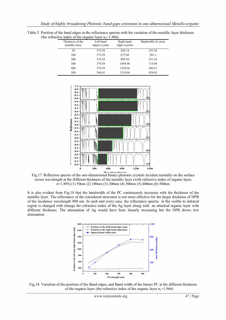
Table.5 Position of the band edges in the reflectance spectra with the variation of the metallic layer thickness
(the refractive index of the organic layer n2=1.966) Thickness of the
metallic layer
Left band
edges λL(nm)
Right band
edges λR(nm)
Bandwidth Δλ (nm)
50 374.58 568.14 193.56
100 374.58 677.68 303.1
200 374.58 905.94 531.36
300 379.59 1094.48 714.89
400 379.59 1228.26 848.67
500 384.61 1218.64 834.03
0 300 600 900 1200 1500
0.0
0.3
0.6
0.9
0.0
0.3
0.6
0.9
0.0
0.3
0.6
0.9
0.0
0.3
0.6
0.9
0.0
0.3
0.6
0.9
0.0
0.3
0.6
0.9
1.2
(f)
(e)
(d)
(c)
(b)
(a)
Wavelength(nm)
Ref
lect
ance
Fig.17. Reflection spectra of the one-dimensional binary photonic crystals incident normally on the surface
versus wavelength at the different thickness of the metallic layer (with refractive index of organic layer,
n=1.895) (1) 50nm (2) 100nm (3) 200nm (4) 300nm (5) 400nm (6) 500nm
It is also evident from Fig.18 that the bandwidth of the PC continuously increases with the thickness of the metallic layer. The reflectance of the considered structures is not more effective for the larger thickness of NPB
of the incidence wavelength 800 nm. In each and every case, the reflectance spectra in the visible to infrared
region is changed with change the refractive index of the Ag layer along with an attached organic layer with
different thickness. The attenuation of Ag would have been linearly increasing but the NPB shows low
attenuation.
0 100 200 300 400 500
400
600
800
1000
1200
1400
1600
1800
Position of the lefth band edges (nm)
Position of the right band edges(nm)
Optical Band width (nm)
Wavelength (nm)
Po
siti
on
of
the
left
an
d r
igh
t b
an
d e
dg
es (
nm
)
300
600
900
1200
Op
tical b
an
d g
ap
(nm
)
Fig.18. Variation of the position of the Band edges, and Band width of the binary PC at the different thickness
of the organic layer (the refractive index of the organic layer n2=1.966)
Study of highly broadening Photonic band gaps extension in one-dimensional Metallo-organic
www.iosrjournals.org 48 | Page
Due to tunability of the refractive index with applied frequency/or wavelength, the enhancement of reflectance
spectra in the Ag-NPB periodic system may lie in the peculiar photonic band gap of metallo-organic photonic
structure which has no tendency to give the propagating modes in the particular frequency region. The periodic structure to increase the number of period ‘N’ of Ag-NPB has concentrated more states on the frequency ranges
of particular photonic bands due to the conservation of the total number of states in between these gaps as
shown in Fig18. Widen bandgap is obtained at the less number of the periods but wideness decreases with
increase the number of the periods in the PC. The maximum number of band gap splitting is more observed at
the higher of periods in the system. More and more number of states of Ag-NPB has been concentrated over a
frequency range of the photonic band structure.
IV. Conclusion 1. In the metal-organic Photonic structure system large reflection at the periodic layer in 500 nm-1000nm
region has been observed due to the organic layer. The reason for the reflectance enhancement in the 1D
MOPS is due to the existence of photonic band gap where no propagating modes are available. Maximum
number of periods affects the density of the reflectance.
2. The study of the reflectance spectra versus thickness of the metallic layer in different region of the
electromagnetic spectrum at the different incident wavelengths are found that the optical band gap increase
and shows the maximum band gap at 500nm
3. Since metal-organic periodic structures show the multiple Bragg scatterings which play an important role
leading to the formation of photonic band gaps like metallic-dielectric photonic crystals.
4. The study of reflectance spectra of the same structure versus the thickness of the NPB layer at different
incidence wavelengths also found the enhanced the optical band gap but less compared to the metallic layer
when the attenuation of the metal is too low. 5. The attenuation of organic and metallic layers is important criteria which gives maximum band gap due to
the variation of the thickness of either organic layer or metallic layer. It means that the absorption can be
enhanced in a periodic structure due to the metal and organic layers; even the attenuation of the metal is too
low in certain frequency region.
6. The low attenuation at infrared region and large thickness of the organic/or metallic layers can also enhance
optical band gap in 1D MOPS system.
Reference [1] Joannopoulos J D, Meade R D, and Winn J N. Photonic Crystals: Molding the Flow of Light, Princeton University Press,
Princeton, NJ, 1995. ISBN 0691037442.
[2] Suthar B, and Bhargava A. Tunable multi-channel filtering using 1-D photonic quantum well structures, Progress In
Electromagnetics Research Letters, 2011, 27: 43-51.
[3] Bhargava A, and Suthar B. Optical switching properties of kerr-nonlinear chalcogenide photonic crystal, J. of Ovonic Research,
2009, 5(6): 187.
[4] Pendry J B, Holden A J, Robbins D J, and Stewart W J. Magnetism from conductors and enhanced nonlinear phenomena, IEEE
Trans. Microwave Theory Tech, 1999, 47: 2075–2084.
[5] Smith D R, Padilla W, Vier D C, Nemat-Nasser S C, and Chultz S. A composite medium with simultaneous negative permittivity
and permeability, Phys. Rev. Lett., 2000,84; 4184-4187.
[6] Sievenpiper D F, Zhang L, Jimenez Broas R F, Alexopolous N G, Yablonovitch E. High-impedance electromagnetic surfaces with
a forbidden frequency band, IEEE MTT, 1999, 47: 2059-2074.
[7] Hinterholzinger F M, Ranft A, Feckl J M, Ruhle B, Bein T, and Lotsch B V. One-dimensional metal–organic framework photonic
crystals used as platforms for vapor sorption, J. Mater. Chem., 2012, 22: 10356.
[8] Srivastava R, Thapa K B, Pati S, and Ojha S P. Omni-direction reflection in one dimensional photonic crystal, Progress In
Electromagnetics Research B, 2008,7: 133-143.
[9] Feng S, Elson J M, and Overfelt P L. Optical properties of multilayer metal-dielectric nano films with all evanescent modes, Optic
Express , 2005, 13: 4113-4124.
[10] Zhang L T, Xie W F, Wang J, Zhang H Z, and Zhang Y S. Optical properties of a periodic one-dimensional metallic-organic
photonic crystal, J. Phys. D: Appl. Phys. 2006, 39: 2373-2376.
[11] Ward A J, Pendry J B, Stewart W J. Photonicdispersion surfaces, J. Phys.: Condens. Matter,1995,7:2217-2224,.
[12] Palik E D. Handbook of Optical Constants of Solids I, II, III, Academic Press Ltd., 1998.
[13] Yeh P. Optical Waves in Layered Media, John Wiley and Sons, New York, 1988.
[14] Guida G, Lustrac A De, and Priou A. An introduction to photonic band gap (PBG) materials, Progress In Electromagnetics
Research, PIER ,2003, 41, 1-20.
[15] Shirota Y, Okumoto K, Inada H.Thermally stable organic light-emitting diodes using new families of hole-transporting amorphous
molecular materials. Synthetic Metals,2000, 111: 387–391.
[16] Tauc J, Grigorovici R & Vancu A. Optical properties and electronic structure of Amorphous germanium, Phys Stat. Sol, 1966, 15:
627.
[17] Markos P and Soukoulis C M. Wave Propagation: From Electrons to Photonic Crystals and Left-handed Materials, Princeton
University Press, New Jersey, 2008.
[18] Yu J, Shen Y, Liu X, Fu R, Zi J, and Zhu Z. Absorption in one dimensional metallo-dielectric photonic crystals, J. Phys.: Conden.
Matter, 2004, 16: L51-L56.
[19] Zhang L T, Xie W F, Wang J, Zhang H Z, and Zhang Y S. Optical properties of a periodic one-dimensional metallic-organic
photonic crystal, J. Phys. D: Appl. Phys. 2006, 39: 2373-2376.