Structural Modulation and Phase Transitions in Melilites
144
Structural Modulation and Phase Transitions in Melilites Dissertation zur Erlangung des Doktorgrades der Naturwissenschaften (Dr. rer. nat.) dem Fachbereich Geowissenschaften der Philipps-Universität Marburg vorgelegt von Zhihong Jia aus der V. R. China Marburg/Lahn, Germany 2005
Transcript of Structural Modulation and Phase Transitions in Melilites
Structural Modulation and Phase Transitions
in Melilites
Dissertation
zur Erlangung des Doktorgrades
der Naturwissenschaften (Dr. rer. nat.)
dem Fachbereich Geowissenschaften
der Philipps-Universität Marburg
vorgelegt von Zhihong Jia
aus der V. R. China
Marburg/Lahn, Germany 2005

Vom Fachbereich Geowissenschaften
der Philipps-Universität Marburg
als Dissertation am 17. 01. 2005 angenommen.
Erstgutachter: Dr. Helmut Rager
Zweitgutachter: Prof. Dr. Werner Massa
Tag der mündlichen Prüfung am 02. 02. 2005

Contents
Contents
1 Introduction......................................................................................................1
2 Structure modulation of melilites ...................................................................3
2.1 General aspects of incommensurability .............................................................3
2.2 The melilite system............................................................................................4
2.2.1 Temperature dependence of the structure modulation.......................................5
2.2.2 The compositional dependence of the structure modulation .............................8
2.3 Mechanisms of the structure modulation in melilites ........................................9
3 Experimental methods...................................................................................13
3.1 Single-crystal growth method and apparatus...................................................13
3.1.1 Double ellipsoid mirror furnace.......................................................................13
3.1.2 Factors affecting singe crystal quality .............................................................16
3.2 Electron microscopy ........................................................................................18
3.2.1 Transmission electron microscopy ..................................................................18
3.2.2 Scanning electron microscopy, energy-dispersive X-ray spectrometry and
wavelength-dispersive X-ray spectrometry .....................................................29
3.3 Electron spin resonance ...................................................................................32
3.4 X-ray diffraction ..............................................................................................34
3.5 Magnetic measurements...................................................................................36
3.6 Other methods..................................................................................................39
3.6.1 Differential scanning calorimeter ....................................................................39
3.6.2 Photoluminescence measurements...................................................................39
4 Results and discussions..................................................................................40
4.1 Synthesis of Ca2MgSi2O7, Ca2CoSi2O7 and Ca2ZnSi2O7 melilites..................40
4.2 Single crystal growth .......................................................................................44
4.2.1 The preparation of a feed rod and a seed crystal .............................................44
4.2.2 Growth of Ca2Mg1-xZnxSi2O7, Ca2Co1-xZnxSi2O7, (Ca1-xSrx)2CoSi2O7 crystals
..........................................................................................................................46
4.3 Investigations of Ca2Mg1-x(Zn, Co)xSi2O7 with modulated structure..............55
4.3.1 The Ca2Mg1-xZnxSi2O7 system.........................................................................55
i

Contents
4.3.2 The Ca2Mg1-xCoxSi2O7 system ........................................................................60
4.3.3 Conclusions......................................................................................................65
4.4 Modulation and phase transitions of Ca2Co1-xZnxSi2O7 in dependence on
temperature and composition...........................................................................66
4.4.1 Crystal growth and characterization ................................................................66
4.4.2 The average structure observed by high-resolution transmission electron
microscopy and corresponding image simulation............................................71
4.4.3 Electron microscope studies of the modulated structure .................................74
4.4.4 The transition from the incommensurate phase to the commensurate lock-in
phase and to the normal phase .........................................................................78
4.4.5 Refinement of the commensurate lock-in structure of Ca2Co0.9Zn0.1Si2O7 .....88
4.4.6 Conclusions......................................................................................................92
4.5 Investigations of the structural modulation of (Ca1-xSrx)2CoSi2O7..................94
4.5.1 Crystal characterization ...................................................................................94
4.5.2 The modulated structure and the transition from the incommensurate to the
normal phase with varying Sr-content .............................................................99
4.5.3 Conclusions....................................................................................................106
4.6 Investigations of Ca2(Mg,Co)Si2O7 doped with Cr and Eu ...........................107
4.6.1 Synthesis and characterization of Ca2MgSi2O7:Cr solid solutions ................107
4.6.2 Synthesis, characterization and optical properties of Ca2Mg(Co)Si2O7:Eu solid
solutions .........................................................................................................110
4.6.3 Conclusions....................................................................................................116
5 Summary and outlook .................................................................................117
6 Zusammenfassung und Ausblick................................................................120
7 References.....................................................................................................123
Appendix A. Lock-in phase of Ca2(Co0.9Zn0.1)Si2O7 refined in s. g. 222 11P
Appendix B. Lock-in phase of Ca2(Co0.9Zn0.1)Si2O7 refined in s. g. _4P .
Appendix C. Abbreviations
Acknowledgements
ii

1 Introduction
1 Introduction
A crystal consisting of atoms repeated regularly in three dimensions has a so-called
translational symmetry, which can be described by one of the 230 crystallographic
space groups. The lattice periodicity is apparent in X-ray, electron or neutron
diffraction patterns which consist of sharp spots located on points of the reciprocal
lattice. Often, additional spots besides the main reflections are observed, they can be
attributed to the existence of various kinds superlattice structures, lattice defects or
structure modulations. Incommensurately modulated crystals are known from, e.g.,
quasi one-dimensional conductors [1], ferroelectrics [2], alloys [3], minerals [4, 5],
composite crystals [6].
Extensive studies have been done on melilite-type compounds with the general
formula X2T1T22O7 to elucidate the nature of the observed incommensurate ordering.
The melilite structure consists of layers formed by T1 and T2 tetrahedra and the larger
X cations located halfway between adjacent layers. The incommensurate modulation
was first described independently by Hemingway et al. [4] and Seifert et al. [5] in
synthetic Ca2MgSi2O7 åkermanite. It was supposed that the misfit between the large X
cations and the sheet-like tetrahedral framework might be responsible for the
modulation. Changing the structural misfit by substitution of other cations or by
temperature varied the amplitude of the modulation and the length of the modulation
vector [7-11]. X-ray refinement suggested that the modulated structure is mPmgpP 124
4
according to the (3+2)-dimensional superspace formalism, and that the modulation is
caused by a displacive shift of the constituent atoms resulting in a rotation and
deformation of the T1 and T2 tetrahedra [12, 13]. These changes appear to be
accompanied by changes of the interlayer X-cation environment in a way that reduces
the coordination number of X from eight to seven or even six [14-17]. It was further
concluded that the flattened T1-tetrahedra surrounded by low-coordinated X cations
show the tendency to form octagonal clusters, and that the arrangement of these
clusters determines the strength of the overall modulation [16, 18, 19].
In spite of the number of studies, the detailed structure of modulated melilite
crystals has not yet been clarified till now. This holds for the atomic configurations
and the correct symmetry relations of the five-dimensional structure as well as the
different aspects of superstructure ordering. The transition from the incommensurate
1

1 Introduction
to the commensurate lock-in phase and the formation of domains during this process
in melilites are also not yet clear. Another open question remains the possible
contribution of occupational modulation in addition to the displacive modulation [9, 15].
Finally, studies of the structural modulation of Co/Zn-melilites are still lacking.
End-members of melilites like Ca2Al2SiO7 and Ca2MgSi2O7 have potential
applications as laser active materials [20, 21] and long-lasting phosphorescent materials [22-24]. Detailed knowledge of the structure is a prerequisite for the exploitation of the
appropriate material. On the other hand, because the melilite family occurs in igneous
rocks which come from continuous crystallization of magma compositions with
falling temperature, investigations of crystals of the melilite system are also important
to understand the formation of rocks.
This work will contribute to a better understanding of the fundamentals of the
structural modulation and its formation mechanisms in melilites as well as of the
correlation between the domain structure formed during phase transition and the
modulation. To begin it was necessary to find out the optimum conditions for growing
high-quality single crystals of the series Ca2Mg1-xZnxSi2O7, Ca2Co1-xZnxSi2O7 and
(Ca1-xSrx)2CoSi2O7 by the floating zone melting technique. Then the aim was to
investigate the variations of the modulation with composition and temperature, and to
find out the features occurring during transitions from the incommensurate phase to
the normal phase and to the low-temperature commensurate phase as well as the
details of the domain formations. Electron microscopy, electron and X-ray diffraction
techniques, X-ray analytic methods as well as differential scanning calorimetry were
applied as the main methods for the present studies. Preliminary investigations were
done to find out the effects of Cr and Eu doping on the structure and the optical
behavior of Ca2MgSi2O7 and Ca2CoSi2O7 melilites.
2

2 Structure modulation of melilites
2 Structure modulation of melilites
2.1 General aspects of incommensurability
As pointed out in the introduction, in crystal diffraction patterns additional
reflections can be observed besides the main lattice reflections, indicating the
existence of additional ordering schemes. Such crystals may have an incommensurate
crystal structure and can not be described by three-dimensional crystallographic space
groups.
An incommensurate crystal can be described in terms of a basic structure with
three-dimensional space group symmetry and a periodic deviation (the modulation)
which in the incommensurate phase has a period that does not fit to the lattice of the
basic space group. According to the different origin causing the modulation, one can
class them as the following:
(1) If the modulation consists of displacements one has a displacively modulated
structure (Fig.2.1.1a);
(2) If the modulation involves a variation of the occupation probability of given
atoms at crystallographic sites of the basic structure one has an occupation-modulated
structure (Fig.2.1.1b);
(3) A system consisting of at least two subsystems whose basis structures are
mutually incommensurate is called an incommensurate composite structure
(Fig.2.1.1c).
Fourier wave-vectors of a modulated crystal phase can be expressed as:
h = ha* + kb* + lc* + mq (2.1.1)
where a*, b*, c* are the basic vectors of the reciprocal lattice of the basic structure, q
is the modulation vector of the reciprocal lattice, and m is integer. In this case the rank
of the quasi-lattice is four and its dimension three. In general, the modulation is
multiperiodic and involves several wave vectors qj. Then, the quasi-lattice to which
the diffraction spots belong is
⎭⎬⎫
⎩⎨⎧
+∗= ∑ ∑= =
3
1 1
*
i
d
jjjii qmahM hi, mj integers (2.1.2)
The rank of the quasi-lattice is 3 + d, where d is called the dimension of the
modulation.
3

2.1 General aspects of incommensurability
Fig.2.1.1 Three types of incommensurate crystal phases. (a) Transversal displacive modulation with wave-vector 0.2881a*; each atom is displaced in the b direction. (b) Occupation modulation: the probability for finding an atom A (full circles) at a lattice position n is given by cos(q ⋅ n), with q = 0.2881a*. In the planes perpendicular to the a axis the atoms A are distributed statistically with this probability. At the remaining positions atoms B (open circles) are found. (c) Composite structure: two lattices are simultaneously present, one with lattice constants a, b and c, the other with a’, b and c, respectively, with irrational a’/a = 1.4085. (Reproduced from Janssen and Janner [25])
Satellite peaks may be temperature dependent. Thus, the incommensurate crystal
phase varies as a function of temperature. Many compounds including melilites
exhibit an incommensurate crystal phase in a certain temperature interval, which may
vary from one to several hundred degrees. Above this interval a normal crystal phase
exists, i.e. the basic crystal structure. At low temperatures the incommensurate crystal
phase may convert into a so called lock-in phase if the wave-vectors of the
incommensurate crystal phase are in mutually fixed rational relations. However, many
compounds behave differently without showing any transition into the lock-in phase.
2.2 The melilite system
The melilite group mainly consists of a solid solution of gehlenite, Ca2Al2SiO7, and
åkermanite, Ca2MgSi2O7, with variable amounts of CaNaAlSi2O7 and Ca2FeSi2O7.
Melilites occur in natural rock assemblages and have the general formula X2T1T22O7.
They have also been synthesized for a wide range of chemical composition, i.e. with
X = Ca, Sr, Ba, Na, La, T1 = Co, Mg, Fe, Cr, Zn, Al, …, and T2 = Si, Al, Ge, Ga,
Be, …[7]. The average structure of melilite, firstly determined by Warren [26] and
revised by Smith [27], consists of layers of corner sharing [T2O4] and [T1O4] tetrahedra,
as shown in Fig.2.2.1a. The eight-fold coordinated X cations provide the connection
between adjacent layers (Fig.2.2.1b) The symmetry of the average structure is
tetragonal with space group mP 124 .
4

2 Structure modulation of melilites
The [T2O4] tetrahedra occur as [T22O7] dimers linked by O1 atom. The four O3
atoms in the layer plane are linked to [T1O4] tetrahedra. The vertices of the dimer
tetrahedra are either both pointing up or both pointing down with respect to the layer
plane. The [T1O4] tetrahedra have one of their binary axes perpendicular to the layer
plane. The two upper corners are linked to the [T22O7] dimer with tops pointing down,
whereas the two lower corners of the [T1O4] tetrahedra are linked to the [T22O7]
dimers with tops pointing up. The resulting sheets are rather thin, and their thickness
is roughly the height of one [T2O4] tetrahedron. This corner share results in an
irregular pentagonal arrangement of tetrahedra. This arrangement forms channels
which are filled with large X-ions located about halfway between the sheets. A side
view of the structure is shown in Fig.2.2.1b.
Fig.2.2.1 Structure of melilite (X2T1T22O7). (a) The [T1O4] and [T2O4] tetrahedra are projected
on the c-plane as squares and triangles, respectively. A subunit containing a [T22O7] dimer is
outlined with dashed lines. The open circles represent the X-ions positioned halfway between the sheets as can be seen in (b). (Reproduced from von Heurck et al., 1992 [28])
2.2.1 Temperature dependence of the structure modulation
In synthetic Ca2MgSi2O7, Hemingway et al. [4] observed that the set of strong main
reflections is accompanied by weak satellite reflections, indicating an
incommensurate modulation. With in situ heating in the transmission electron
microscope, the intensity of the satellite reflections decreased significantly at
temperatures above 358K and disappeared completely at about 580K. Hemingway et
5

2.2 The melilite system
al. concluded that this behavior is associated with local displacements of calcium ions
from the mirror plane and accompanying distortion of the tetrahedral sheets.
The synthetic series Ca2Mg1-xFexSi2O7 (0 ≤ x ≤ 0.7) exhibit at room temperature an
incommensurate phase [5]. Satellite reflections along [100] and [110] in the reciprocal
lattice are observed and the distance of the satellites decreases with temperature, thus
the corresponding wavelength of the modulation, which is incommensurate with
respect to the average melilite structure, increases with temperature. Increasing
temperature leads to increasing diffuseness of all satellites, but the effect is stronger
for satellites on [100] than on [110]. The satellite peaks disappear at 130°C. When
lowering the temperature the satellites reappear at the same transition temperature and
attain the same intensity and position as before heating. This indicates that the phase
transition is completely reversible.
Schosnig et al. [11] investigated the temperature dependence of the phase transition
from the normal to the incommensurately modulated structure of (Ca1-xSrx)2MgSi2O7
(x = 0.04, 0.08, 0.16, and 0.22) åkermanites by electron diffraction. The value of the
modulation wavelength λ calculated from the corresponding patterns at different
temperatures reveals that the change of the modulation wavelength also strongly
depends on temperature.
The variation and disappearance of the satellites with increasing temperature up to
355K corresponds to the transition from the incommensurate to the normal phase. The
temperature dependent shift of the satellite reflections and the fact that
incommensurate phases are often intermediate between a high temperature parent
structure and a low temperature superstructure led to the prediction of a
commensurate low temperature phase. This has been proved by Riester and Böhm [29]
on the basis of the investigation of Ca2CoSi2O7 between 30K and 600K using X-ray
single crystal diffraction.
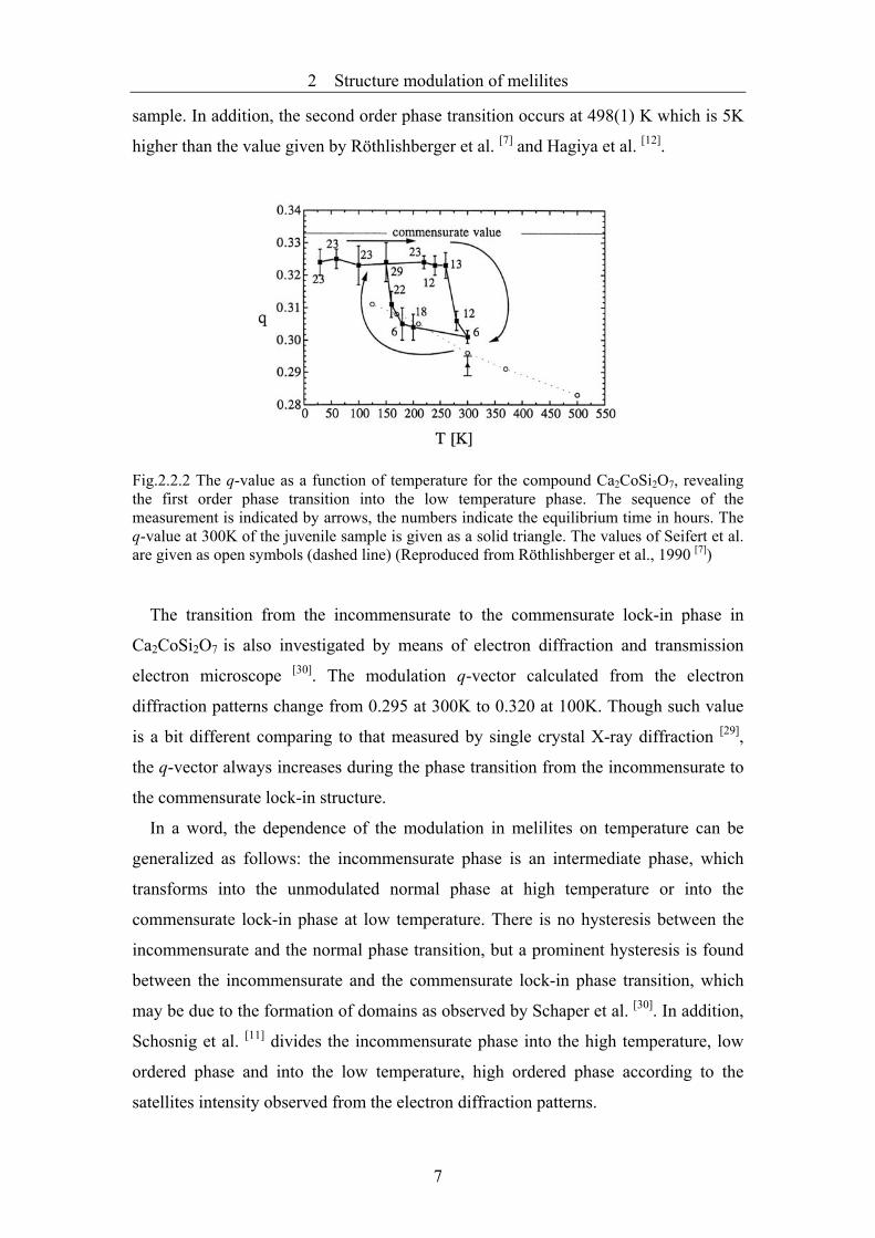
In Fig.2.2.2 the temperature dependence of the q-value is shown. The phase
transition between the incommensurate and the commensurate lock-in structure is
characterized by a prominent hysteresis, which spans over 110K. The low temperature
phase transition is observed at a higher temperature than predicted by Seifert and
Röthlisberger. The cause for this may be the lack of thermodynamical equilibration in
their experiments or just a difference in the thermal history during the synthesis of the
6
2 Structure modulation of melilites
sample. In addition, the second order phase transition occurs at 498(1) K which is 5K
higher than the value given by Röthlishberger et al. [7] and Hagiya et al. [12].
Fig.2.2.2 The q-value as a function of temperature for the compound Ca2CoSi2O7, revealing the first order phase transition into the low temperature phase. The sequence of the measurement is indicated by arrows, the numbers indicate the equilibrium time in hours. The q-value at 300K of the juvenile sample is given as a solid triangle. The values of Seifert et al. are given as open symbols (dashed line) (Reproduced from Röthlishberger et al., 1990 [7])
The transition from the incommensurate to the commensurate lock-in phase in
Ca2CoSi2O7 is also investigated by means of electron diffraction and transmission
electron microscope [30]. The modulation q-vector calculated from the electron
diffraction patterns change from 0.295 at 300K to 0.320 at 100K. Though such value
is a bit different comparing to that measured by single crystal X-ray diffraction [29],
the q-vector always increases during the phase transition from the incommensurate to
the commensurate lock-in structure.
In a word, the dependence of the modulation in melilites on temperature can be
generalized as follows: the incommensurate phase is an intermediate phase, which
transforms into the unmodulated normal phase at high temperature or into the
commensurate lock-in phase at low temperature. There is no hysteresis between the
incommensurate and the normal phase transition, but a prominent hysteresis is found
between the incommensurate and the commensurate lock-in phase transition, which
may be due to the formation of domains as observed by Schaper et al. [30]. In addition,
Schosnig et al. [11] divides the incommensurate phase into the high temperature, low
ordered phase and into the low temperature, high ordered phase according to the
satellites intensity observed from the electron diffraction patterns.
7

2.2 The melilite system
2.2.2 The compositional dependence of the structure modulation
Besides the dependence of the modulation in melilites on temperature, the
composition of melilites likewise influences the modulation. This has been
investigated in detail by synthetic melilites on the join Ca2MgSi2O7 (åkermanite) –
Ca2FeSi2O7 (iron åkermanite) [5]. The modulation wavelength decreases with
increasing Fe content in tetrahedral Mg sites. In pure Ca2MgSi2O7 all satellite peaks
are sharp. With increasing Fe content the intensity between the satellites on [100] and
[110] becomes diffuse forming a ring around the main peaks.
A compilation of different synthetic melilite-type compounds including phase-
transition temperatures, synthesis temperature and investigation techniques is given
by Röthlishberger et al. [7]. The incommensurate phase and its transition to the
unmodulated normal melilite structure can be followed by a variety of techniques,
such as calorimetry and single-crystal X-ray diffraction [4], 57Fe Mössbauer
spectroscopy [5], 29Si MAS NMR [31]. However, transmission electron microscopy and
electron diffraction provide the most direct and sensitive information [4]. Most of the
observed phase transition data are therefore based on electron diffraction
measurements.
Fig.2.2.3 Structural stability field of X2TSi2O7 end-member melilites as a function of the cation radii [X] and [T]. Filled circles: melilite structure; filled triangles: Ba2CuSi2O7 structure type; filled squares: melilite structure, modulated at room temperature; unfilled square: metastable melilite [32]; unfilled circles: no compound of this stoichiometry. The stippled area defines the range of compositions, including solid solution series, in which the melilites are modulated at room temperature (Reproduced from Röthlishberger et al., 1990 [7]).
8

2 Structure modulation of melilites
For X2TSi2O7 melilites the structural stability diagram in terms of ionic radii of X
and T cations is taken from Röthlishberger et al. [7] and shown in Fig.2.2.3. The field
of modulated melilites at room temperature is indicated. As hypothesized by Seifert et
al. [5], the modulated phases are restricted to an area close to the border of the melilite
structural field towards larger T and smaller X cations. The end-member melilites
Ca2TSi2O7 with T = Fe2+, Mn and Cd are not stable. With increasing rT an increasing
amount of Sr substituting for Ca is required to stabilize the particular melilite structure.
The incommensurately modulated phases extend in general to higher Sr contents with
larger rT, but for rT > rFe2+ the field of the modulated structures is truncated by the
overall instability of such melilites of high Ca contents.
The effects of more complex substitutions on the stability of the modulated phase
can be rationalized as follows. Starting from Ca2MgSi2O7, the “gehlenite” substitution
2Al for Mg + Si will decrease the average tetrahedral radius from 0.363 to 0.347Å.
Similarly, starting from Ca2ZnGe2O7, the 2Ga for Zn + Ge substitution decrease the
average tetrahedral radius from 0.460 to 0.443Å. The observed decrease in stability of
the modulated phase upon these substitutions is consistent with the above deductions
of Seifert et al. On the other hand, the substitution of Fe3+ + Al for Mg + Si increases
the average tetrahedral radius from 0.363 to 0.383Å, but instead of the expected
stabilization of the incommensurate structure, the modulation disappears at room
temperature.
In general, the transition temperature, TN-IC, from the unmodulated high-
temperature structure to the incommensurately modulated structure strongly depends
on the composition of the phase. TN-IC increases with increasing ionic radii of the two
types of tetrahedrally-coordinated cations by increasing the dimensions of the
tetrahedral sheet. The concept of a misfit between the size of the interlayer cation and
the size of the tetrahedral sheet is used to explain the absence of an incommensurate
phase in Ba- and Sr-melilites [33].
2.3 Mechanisms of the structure modulation in melilites
Since the phenomenon of the structural modulation was found in melilites [4],
scientists have been devoting themselves to pursue the nature causing modulation. By
substituting different ions for X or T in X2T1T22O7 melilites Seifert et al. [5] proposed
9

2.3 Mechanisms of the structure modulation in melilites
that the incommensurate phase is based on the misfit between the tetrahedral
(T1Si2O7)4-sheets and the Ca2+ ions.
A first structural model for the incommensurately modulated melilites has been
presented by van Heurck et al. [28] on the basis of their transmission electron
microscopy investigations of Ca2ZnGe2O7. Their model consists of commensurately
modulated micro-domains that are separated by antiphase boundaries. Statistical
fluctuations of the size of such domains yield an incommensurate average of the
modulation period. The domains are characterized by octagonal arrangements of Zn-
tetrahedra which form various ordering schemes and vary with temperature.
A structure determination for the incommensurate structure of Ca2CoSi2O7 from X-
ray data in the (3+2)-dimensional space has been reported by Hagiya and Ohmasa [12].
The satellites indicate that the modulation is two-dimensional with wavevectors q1 =
α (a* + b*), q2 = α (-a* + b*). All reflections could thus be written in terms of five
integers hklmn and five vectors in the five-dimensional expression [34] h = ha* + kb*
+ lc* + mq1 + nq2. Using the least-squares program REMOS developed by Yamamoto [35] the modulated structure of Ca2CoSi2O7 has been refined according to the
multidimensional treatment.
The Ca-O bond lengths depend on the Ca coordination. The SiO4 tetrahedron does
not behave as a rigid body, i.e. the distortion of the Si-O bonds is variable throughout
the crystal in agreement with the interpretation of the 29Si NMR spectra observed by
Merwin et al. [31] and of the Mössbauer spectra measured in synthetic iron-bearing
Ca2MgSi2O7 [5]. Variations of the Co-O bond lengths in the T1O4 tetrahedra show a
feature different from those of the Si-tetrahedra. All four Co-O bond lengths change
simultaneously. A histogram of the mean Co-O bond lengths shows two peaks which
probable correspond to a compressed and a normal Co-tetrahedra.
Kusaka et al. [18] have studied the details of the incommensurate structure of
Ca2(Mg0.55Fe0.45)Si2O7 and Ca2CoSi2O7, and proposed that these structures are
characterized by an octagonal arrangement of bundles along the c-axis that are
composed of four arrays of six-coordinated Ca polyhedra and a central array of T1O4
tetrahedra. The ratio of the six-coordinated Ca sites to all Ca sites in Co-åkermanite
(28.5%) is larger than that in Ca2(Mg0.55Fe0.45)Si2O7 (17.8%). The distribution and the
number of the octagons in these bundles vary with the modulation wavelength [36].
10

2 Structure modulation of melilites
The structure determination of the lock-in phase of synthetic Ca2CoSi2O7 elucidates
the driving forces of the modulation in melilites [16]. Two approaches have been
applied: a conventional refinement using a (3×3)-fold superstructure and a refinement
in the (3+2)-dimensional superspace. The representation of the lock-in structure
shows the distortion of the tetrahedral layer and the correlated displacements of
calcium atoms. The calculations of the bond lengths revealed six-, seven-, and eight-
fold oxygen coordinations for calcium. The atoms (Ca, Si, O(2)) are significantly
displaced from their former special positions in the non-modulated phase. The
displacement patterns of Ca and Co become apparent in the partial Fourier synthesis
of the satellite reflections. Within the tetrahedral layer the largest displacements are
observed for the bridging oxygen atoms O(1) and O(3). The distortion of the
tetrahedral layer is based mainly on rotations of the SiO4- and CoO4-tetrahedra. The
rotational distortions in the tetrahedral layer are accompanied by displacements of the
central atoms. The bond valence calculations revealed the expected valences for Co2+
and Si4+. The calculated valence sums for all nine symmetrically independent Ca
atoms, however, are too small. This can be explained by the high degree of distortion
of the Ca coordination.
In the non-modulated phase calcium is coordinated by eight oxygen atoms in a
distorted quadratic antiprism with four shorter and four longer bond distances. In the
incommensurate phase the increase of the distortion of the calcium coordination
polyhedra results in six-fold Ca coordination [12]. For the lock-in structure the
coordination of 2/3 of Ca sites is lower than eight-fold. The six- and seven-fold
coordinated calcium atoms show the largest distortion of the structure. The strong
distortion of the tetrahedral layer is obvious because the tilt angle can be up to 28° [16].
The number of lower coordinated calcium increases with decreasing temperature. This
process starts in the non-modulated phase when the thermal vibrations become too
small for a proper fit of calcium in the quadratic antiprism. At temperatures above the
normal to incommensurate phase transition the distortions are distributed statistically
and can be observed spectroscopically [5].
As suggested by Kusuka et al.[37] the six-fold coordination Ca form an ordered
distribution of clusters around the CoO4 tetrahedra, forming centered octagons in the
(3×3×1) super cell. The clusters with six-fold coordinated calcium sites are ordered in
11

2.3 Mechanisms of the structure modulation in melilites
domains with an average size of about (7×7×1) unit cells of the basic structure. The
average domain size is temperature dependent.
Such a centered octagonal arrangement agrees with TEM observations of
incommensurately modulated Ca2ZnGe2O7 at room temperature [28]. The centered
octagonal arrangements vary with temperature. The change from an octagonal
arrangement with diameter φ = 4 subunits and a tentative overlap of these units in the
incommensurate phase to a centered octagonal arrangement with diameter φ = 3
subunits in the lock-in phase is confirmed by high-resolution transmission electron
microscope (HREM) images [30]. In the lock-in phase the octagonal arrangements are
regarded as completely overlapping. This leads to a more general approach of
understanding of the structural modulation in melilites. The driving force for the
modulation in order to release internal stress leads to the formation of domains with
clusters arranged in octagons which represents an energetically favorable pattern.
On the basis of the results derived from an electron microscope imaging and
electron diffraction study, Jiang et al. [9] showed that an occupational modulation also
contributes to the overall modulation characteristics, as a consequence of the ordered
distribution of Sr. Accordingly, Bagautdinov et al. [15] found a sinusoidal form of the
occupancy modulation of Sr and Ca in the incommensurately modulated structure of
(Sr0.13Ca0.87)2CoSi2O7.
12

3 Experimental methods
3 Experimental methods
3.1 Single-crystal growth method and apparatus
3.1.1 Double ellipsoid mirror furnace
The floating zone (FZ) melting method is developed from the zone melting
technique, which is used to refine solid materials. In this method a molten zone is held
between two vertical collinear solid rods by its surface tension. Normally,
temperatures > 1000°C should be attainable for melting a raw material, thus the heat
source and the design to focus energy are very important. The ellipsoid mirror furnace
using focused light provides an efficient and compact way for a local heating,
especially for high temperature applications. The two main components of the
ellipsoid mirror furnace are the ellipsoidal reflectors and the lamps. The simplest
geometry for a mirror furnace is a closed ellipsoid of rotation with one lamp, so-called
mono-ellipsoid mirror furnace. If such a furnace is equipped with a device providing
translation and rotation movements of the raw material rod it is also suitable for
crystal growth experiments.
The application of such a mono-ellipsoid furnace is limited. The available radiation
energy is determined by the power rating of the lamp. A larger filament of the lamp
could deliver more power but decreases the furnace performance because of worse
focusing properties. Therefore, a two-ellipsoid arrangement consisting of two
ellipsoids has been developed.
A double-ellipsoid is to be preferred because it provides a much better peripheral
thermal distribution of energy than a mono-ellipsoid, although the latter has maximum
thermal efficiency. The double-ellipsoid is especially suitable for high-temperature
crystal growth because the power needed to melt a sample is divided up between two
halogen lamps. The small loss in efficiency is far outweighed by the fact that two
lamp filaments of favorable size can be operated at an electrical power rating far
below breakdown, resulting in a longer lamp life and a safer operation of the furnace.
Considering the demands for high efficiency, thermal symmetry, good focusing
properties and technical feasibility, a double-ellipsoid arrangement with axes a = 90
mm and b = 80 mm (b/a = 0.88) has usually been used.
13

3.1 Single-crystal growth method and apparatus
For all experiments of single crystal growth we used a double-ellipsoid mirror
furnace shown in Fig.3.1.1. It consists of (1) growth furnace; (2) pulling-rotation
system; (3) cooling unit; (4) visualizing system and (5) power supply system. If the
furnace is equipped by a sealed system, crystals can also be grown in protecting
atmospheres.
Fig.3.1.1 A double-ellipsoid mirror furnace. Numbers 1-5 see text.
The growth furnace (see (1) in Fig.3.1.1) is the most important part in the whole set
ups. The enlarged cross-section scheme is shown in Fig.3.1.2. It includes two
ellipsoidal mirrors. There is one halogen lamp (120 V, 1 kW) on each side. The
radiation heat from two halogen lamps is reflected by the ellipsoidal mirrors and
focused on an area of ca. 8mm length, which is the high temperature zone. Based on
the output of the halogen lamp a maximum temperature of about 2000°C can be
reached. This temperature is higher than the melting point of many inorganic
compounds and, therefore, this furnace can be used for synthesis of many kinds of
14

3 Experimental methods
compounds. The growth chamber is a long quartz tube with 2.8 cm diameter and 50
cm length.
Fig.3.1.2 A scheme of mirror furnace. L – Halogen lamps; S – Melting zone; Q – Quartz tube. (a = 90mm, b =c =80mm, b/a = 0.88)
The rotation and translation (see (2) in Fig.3.1.1) of the rod as well as of the seed
crystal are controlled independently through four micro-stepping motors. Normally,
the rod is mounted on the upper shaft and the seed crystal is fixed on the lower one.
By controlling the traveling speed of these two parts, crystals with different diameter
can be grown. The initial touch between the seed crystal and the molten raw material
is very critical for the formation of a stable interface.
The rotation equipment with different adjustment steps enables to choose a suitable
rotation speed. In course of growing a crystal, a concave or convex interface will be
formed due to the properties of the polycrystalline raw material. But these interfaces
do not benefit to grow a single crystal. Therefore, the relative rotating speed is
adjusted to get a relative flat interface.
A good cooling unit (see (3) in Fig.3.1.1) is necessary for running the mirror
furnace at high temperatures. Because the lamps give off plenty of heat energy during
growing process, the lamp holder can reach very high temperatures, which is
disadvantageous for long-time crystal growth. Also, the mirror furnace absorbs less
amount of infrared radiation and is getting hot. The cooling water cycle around two
15

3.1 Single-crystal growth method and apparatus
halogen lamps and the mirror furnace is used to keep an acceptable temperature
during the crystal growth.
A CCD-camera equipped with a monitor (see (4) in Fig.3.1.1) is used for watching
the whole growing process. Visualization enables to modify growth parameters during
growing and, hence, to gain high quality single crystals. It is especially helpful for the
adjustment of the stable interface. The FZ melting method combined with a
visualizing system is the most prominent feature comparing to the Czochralski and the
Bridgman-Stockbarger method.
The required temperature of the zone can be obtained by regulating the input
voltage (see (5) in Fig3.1.1) of the two halogen lamps. It should be noted that the
position and the shape of the lamp can affect, for example, the zone area, the
maximum temperature, the temperature gradient etc. As we know, the temperature
gradient is absolutely critical for the quality of single crystals; therefore, the position
of the lamp is adjusted and fixed before starting the growth procedure.
3.1.2 Factors affecting singe crystal quality
As outlined above, a double-ellipsoid mirror furnace is a good choice to grow
single crystals using the FZ melting method. However, there are several factors which
affect the growth of high quality crystals and, therefore, have to be considered during
growing process.
The zone length is one of the most important operational parameters. From the
condition of the stability the inward pressure on the planar surface of the liquid due to
surface tension should be equal at all points and opposite to the pressure exerted by
the liquid head. It is shown that the maximum height of the liquid, lm, which can be
supported in a floating zone technique, is given by the expression [38]
glm ρ
γ8.2≈ (3.1.1)
where γ is the surface tension of the liquid; ρ is the density of the liquid and g is the
gravitational acceleration. The maximum height of the liquid is related to the radius of
the rod, which is shown in Fig.3.1.3.
In general, lm increases with increasing radius of the rod. It should be noted that this
curve does not indicate any upper limit on the diameter of the rod. It must be
emphasized that equation (3.1.1) provides only a guide line for the selection of the
16

3 Experimental methods
zone length. The actual shape and the stability of the zone is greatly modified by the
degree of stirring and the thermal conductivity of the solid rod because these
parameters affect the curvature of the solid/liquid interface.
Fig.3.1.3 Variation of a maximum stable height, lm, of a floating zone versus radius, r, for cylindrical rods. (Reproduced from Heywang, 1956 [38])
The thickness of the diffusion layer at the solid/liquid interface is a function of
growth velocity. Therefore, the vertical zone velocity is one of the determining factors
for the shape of the solid/liquid interface. The onset of interface stability such as
constitutional supercooling is inherently dependent on the zone vertical-moving
velocity, the concentration of the solute and the temperature gradient at the
solid/liquid interface. It is therefore necessary for a homogeneous single phase single
crystal production to select the vertical-moving velocity with due care. Generally
speaking, slower growth rates are advantageous for producing perfect crystals. On the
other hand fast growth speeds may enable one to avoid interface instabilities simply
because a fast growth does not permit the diffusion processes to build an enhanced
impurity layer at the interface.
The temperature gradient at the solid/liquid interface is an important parameter
governing the onset of interface instability. A correct combination of the imposed
temperature gradient and traverse speed is essential for avoiding micro-segregation.
The imposed temperature gradient depends on the nature of the heat source, thermal
conductivity of the ingot material and other modes of heat losses. It should be noted
that the magnitude of the temperature gradient would affect the zone length and the
degree of mixing in the zone.
17

3.2 Electron microscopy
3.2 Electron microscopy
3.2.1 Transmission electron microscopy
3.2.1.1 Image formation in the TEM
The image formation in the electron microscope consists of three consecutive
processes: electron scattering in the specimen and formation of the exit wave,
formation of diffracted beams at the back focal plane of the objective lens, and
formation of an image in the image plane. Accordingly, the electron optical system of
a TEM can be approximated by the schematic principle shown in Fig.3.2.1.
Fig.3.2.1 Electron optical system of image formation in TEM. Ψi – the incident electron wave function; Ψe – the exit-surface wave function; Ψd – the diffraction pattern; Ψd´ – the corrected diffraction pattern; Ψim – the wave function in the image plane (according to [39]).
The electron wave ψi striking on the specimen depends on the characteristics of the
electron source (gun) and the condenser lens and can be described as a plane wave of
the form
( ikri −Ψ=Ψ exp0 ) (3.2.1)
where k is the wave vector and |k| = 2π/λ the wave number, r is the position vector.
The wavelength λ of the incident wave is determined by the principle of conservation
of energy of an electron in a potential field U:
18

3 Experimental methods
meUh
mvh
2==λ (3.2.2)
where h is Planck’s constant, ν is the velocity of the electron, m and e are the electron
mass and charge, respectively. Taking into account the relativistic variation of the
mass of the electron at high energies the relativistic mass of an electron can be
expressed as
⎟⎟⎠
⎞⎜⎜⎝
⎛−
=
2
2
0
1c
mm
ν (3.2.3)
where m0 = electron rest mass, c = velocity of light. Thus, the equation (3.2.2) has to
be rewritten as
rmeUh
2=λ (3.2.4)
where
202
00 2
Ucm
eUU r ⎟⎟⎠
⎞⎜⎜⎝
⎛+= (3.2.5)
where Ur is the relativistic accelerating voltage. The equation (3.2.4) shows that the
electron wavelength λ relates to the accelerating voltage. Table 3.2.1 lists values of
the electron wavelength and the interaction constant σ (see equation 3.2.7) for a
number of selected accelerating voltages.
Table 3.2.1 Electron wavelength λ and interaction constant σ at different accelerating voltage V.
Accelerating Voltage, V (kV)
Wavelength, λ (nm)
Interaction constant, σ (V-1 nm-1)
100 0.00417572 0.0100871 200 0.00250793 0.0072884 300 0.00196875 0.0065262 400 0.00164394 0.0061214 600 0.00125680 0.0057072 800 0.00102695 0.0055030 1000 0.00087192 0.0053850 1250 0.00073571 0.0052956 1500 0.00063745 0.0052397 2000 0.00050432 0.0051760 2500 0.00041783 0.0051423 3000 0.00035693 0.0051223
19

3.2 Electron microscopy
Within a crystal, the wavelength of the incident electron wave will be changed by
the crystal potential ϕ(r) from λ to λ´:
( ))(2 rUmeh
r ϕλ
+=′ (3.2.6)
When the electron wave passes through a thin crystal it undergoes a phase shift
which depends on the projected potential in the z-direction. This is illustrated in
Fig.3.2.2. The mean inner potential of a sample usually increases with increasing
atomic numbers present, and takes values in the range of a few volts to about 30V.
Fig.3.2.2 The electron wave illustrated in two cases passing through a specimen. The wave passing through the centre of an atom (where the potential is high) has its wavelength reduced and so suffers a phase advance relative to the wave passing the specimen between the atoms which experiences little change in its wavelength. (reproduced and processed according to [40]).
The complex exit wave function can be written as
[ ])()(exp rrie µσϕ −−=Ψ (3.2.7)
with µ(r) representing an absorption function and σ the so-called interaction constant,
2
2hmeλπσ = with relativistically corrected values for λ. σ generally decreases with
increasing acceleration voltage, see Table 3.2.1.
Equation (3.2.7) describes the specimen as a strong phase object. Further
simplification for very thin specimens and neglecting considerable absorption is
known as the weak phase object approximation (WPOA):
20

3 Experimental methods
)(1),( riyxe σϕ−≈Ψ (3.2.8)
which assumes only kinematical scattering and ignores dynamical scattering in the
specimen. The essential meaning of equation (3.2.8) is that the amplitude of a
transmitted wave is a linear function of the projected potential of the specimen.
The complex wave amplitude ψd in the back focal plane of the objective lens is
obtained by Fourier transformation of the transmission function:
[ ])().( rFivud ϕσδ −=Ψ (3.2.9)
where F represents the Fourier transformation. δ is a delta function which represents
the unscattered wave (i.e. the direct beam). However, equation (3.2.9) does not take
into account the additional phase shift due to the various aberrations (spherical,
chromatic, astigmatism) of the electron beam in the electron microscope. Spherical
aberration is introduced by the contrast transfer function (CTF)
[ ),(exp),(),( vuivuAvuT ]χ= (3.2.10)
where A(u,v) is the aperture function and χ (u,v) the phase shift due to lens aberrations.
Considering only the spherical aberration (Cs), and combining it with a term for the
focus error ∆f we obtain for the phase shift χ (u,v)
⎟⎟⎠
⎞⎜⎜⎝
⎛∆+=
242 2244 ufuCs
λλλπχ (3.2.11)
Relation (3.2.11) emphasizes the following particular aspects:
1) It is possible widely to compensate for the spherical lens error by choosing an
appropriate defocus value;
2) Defocusing allows phase contrast imaging of the object by making visible the
phase shift induced by the object potential.
Including the aberration effects, the wave amplitude in the back focal plane can be
written
[ ] [ ]),(exp),()().( vuivuArFivud χϕσδ −=Ψ ′ (3.2.12)
Inverse Fourier transformation of equation (3.2.12) leads to the complex image
amplitude Ψim
[ ] [ )exp()(1 ]χϕσ iAFrFiim ⊗−=Ψ (3.2.13)
where ⊗ is the symbol of convolution, and finally, the image intensity is obtained as 2
imI Ψ=ΨΨ= ∗ (3.2.14)
21

3.2 Electron microscopy
Carrying out the multiplication in equation (3.2.14) it becomes evident that only the
imaginary part of (3.2.10) contributes to the image intensity, i.e. only sinχ is
responsible for the final image contrast. sinχ is a complicated curve that depends on
the lens quality of the microscope (Cs) and the so-called “Scherzer defocus” ∆f, a
measure of the resolution power of the microscope. Fig.3.2.3 shows the contrast
transfer function of a JEM 3010 high-resolution TEM with LaB6 cathode mainly used
in this work. The microscope provides a point resolution of 0.167nm.
Fig.3.2.3 Phase contrast transfer function of a JEM 3010 microscope operated at 300kV.
3.2.1.2 Practical aspects of diffraction contrast
Besides the phase contrast outlined above, diffraction contrast which is one form of
the amplitude contrast is often used in imaging defect structures. When electrons with
wavelength λ pass through a crystal of lattice spacing d diffracted waves will be
produced at angles 2θ according to the Bragg condition, λθ =sin2d (See also 3.4).
The diffraction waves form diffraction spots in the back focal plane (Fig.3.2.4). By
choosing different diffraction spots using the objective aperture diffraction contrast
images are obtained.
22

3 Experimental methods
Bright-field (BF) and dark-field (DF) images will be formed when an objective
aperture selects only the spot formed by the direct electron beam (Fig.3.2.4a) or any
diffracted spots (Fig.3.2.4b). The high-resolution image is obtained by choosing both
kinds of diffracted spots (Fig.3.2.4c). It emphasizes the information corresponding to
the selected diffracted spots. To get strong diffraction contrast the specimen is tilted to
two-beam conditions.
Fig.3.2.4. Three observed modes in electron microscopy using an objective aperture. The
center of the objective aperture is assumed to be set to the optical axis. (a) bright-field method;
(b) dark-field method; (c) high-resolution electron microscopy (reproduced from [41]).
3.2.1.3 Structure factor and crystal potential
The introduction of the structure factor concept is most important in solving crystal
structures from high-resolution images and diffraction patterns. The structure factor is
defined as
∑=
⋅=N
jjj ruiufuF
1)(2exp)()( π (3.2.15)
where fj(u) is the atomic scattering factor for atom j and u are coordinates of atom j in
three dimensional direction. N is the number of atoms in the unit cell. rj is the position
vector.
The equation (3.2.15) means that the amplitude of the scattering is influenced by
the type of the atom, its position in the unit cell and the specific atomic phases
contributing to the discrete reciprocal lattice. F(u) is complex and consists of the
amplitude |F(u)| and the phase φ(u)
23

3.2 Electron microscopy
[ )(exp)()( uiuFuF φ= ] (3.2.16)
The phase depends on the origin chosen of the unit cell (in centro-symmetic
structures it is always in the center of symmetry).
The crystal potential ϕ(r) introduced in equation (3.2.6) is closely related to the
structure factor F(u):
[∑ ⋅−Ω
= )(2exp)()( ruiuFr πσ
]λϕ (3.2.17)
where σ = interaction constant, Ω = unit cell volume. Therefore, if both the
amplitudes |F(u)| and the phase φ(u) of the structure factor are known for all
reflections u, the potential ϕ(r) can be determined. This is the key principle in the
analysis of unknown crystals within the bounds of Electron Crystallography [42].
3.2.1.4 Image simulation
Image simulation was originally developed for interpreting experimental high-
resolution TEM images because high-resolution images are affected not only by
various aberrations but also by dynamical diffraction effects. Interpretation of atomic
resolution images taken by HRTEM makes image simulation necessary for
confirming the precise atomic positions. Two methods are available [40], namely, the
Bloch wave and the multislice method. The Bloch wave method solves directly the
time independent Schrödinger equation and the exit wave function of the crystal is
obtained. The multislice method is based on the physical optics approach [43]. The
crystal of the thickness t is sliced into many thin slices of small thickness ∆t. For each
slice the potential is projected onto a plane and the corresponding projected potential
is calculated. The propagation of the electron wave from the exit surface of one slice
to the incident surface of the next slice is considered as a Fresnel propagation in
vacuum. These two methods may be applied in complementary cases. However, the
multislice approach is more frequently used, e.g. in the JEMS software package
developed by Stadelmann (http://cimesg1.epfl.ch/CIOL/asu94/ICT_1.html).
3.2.1.5 Instrumentation
In this work mainly a JEOL 3010 TEM with LaB6 as electron source operated at
300 keV was used. The attainable point and lattice resolutions of the microscope are
24

3 Experimental methods
0.167nm and 0.14nm, respectively. The microscope is equipped with a 2048 ×2048
CCD camera for image acquisition. The sample can be tilted in two directions along x
and y axis up to 20° using the double tilt specimen holder. Phase transitions can be
investigated by a double tilt cooling specimen holder (636-DH) in which the sample
can be cooled down, using liquid nitrogen, to a temperature of about -170°C. The
temperature stability is better than ± 1°C in the range from -170°C to -130°C.
The JEOL-ARM1250 „Atomic-Resolution Microscope” at MPI in Stuttgart
operating at an accelerating voltage of 1250 keV was used for detecting atomic
positions in the studied systems. A point resolution of 0.12 nm can be reached with
the “side-entry” goniometer in this microscope.
A cryo-high-resolution microscope JEM-4000SFX operating at 400 keV was also
used for additional very low-temperature measurements at liquid He temperature.
3.2.1.6 Specimen preparation for TEM
Because of the strong interaction of electrons with matter, very thin specimen (<
100Å) should be used for high resolution imaging. Preparation of thin specimens with
extremely smooth surfaces is highly important for any TEM investigation, especially
for high-resolution TEM structural studies. Such a specimen can be prepared by ion
beam milling at low incident angles.
For our TEM investigations, high-resolution structural image of (001) plane is
helpful for studying the modulated structure, so the c-axis of the sample should be
parallel to the direction of the electron beam, so several steps were taken before final
ion milling as shown in scheme 3.2.1.
Cutting Fixing
The precession method [44] had been used to orient the specimen. According to the
reflection dots on the film, we adjusted the goniometer in three directions to make the
c-axis of the crystal parallel to the direction of the X-ray beam.
Scheme 3.2.1 The pre-preparation process before ion milling.
Grinding Polishing Orientating
25
3.2 Electron microscopy
After orientation the crystal of 1mm × 1.8mm size was cut from the bulk material.
A Well Precision Diamond Wire Saw (Model 3242) was used for this cutting. The
diameter of the wire is 0.3mm. The cutting speed and strength depend on the nature of
the material. For brittle materials a small cutting speed and strength were applied;
otherwise, the material got easily broken.
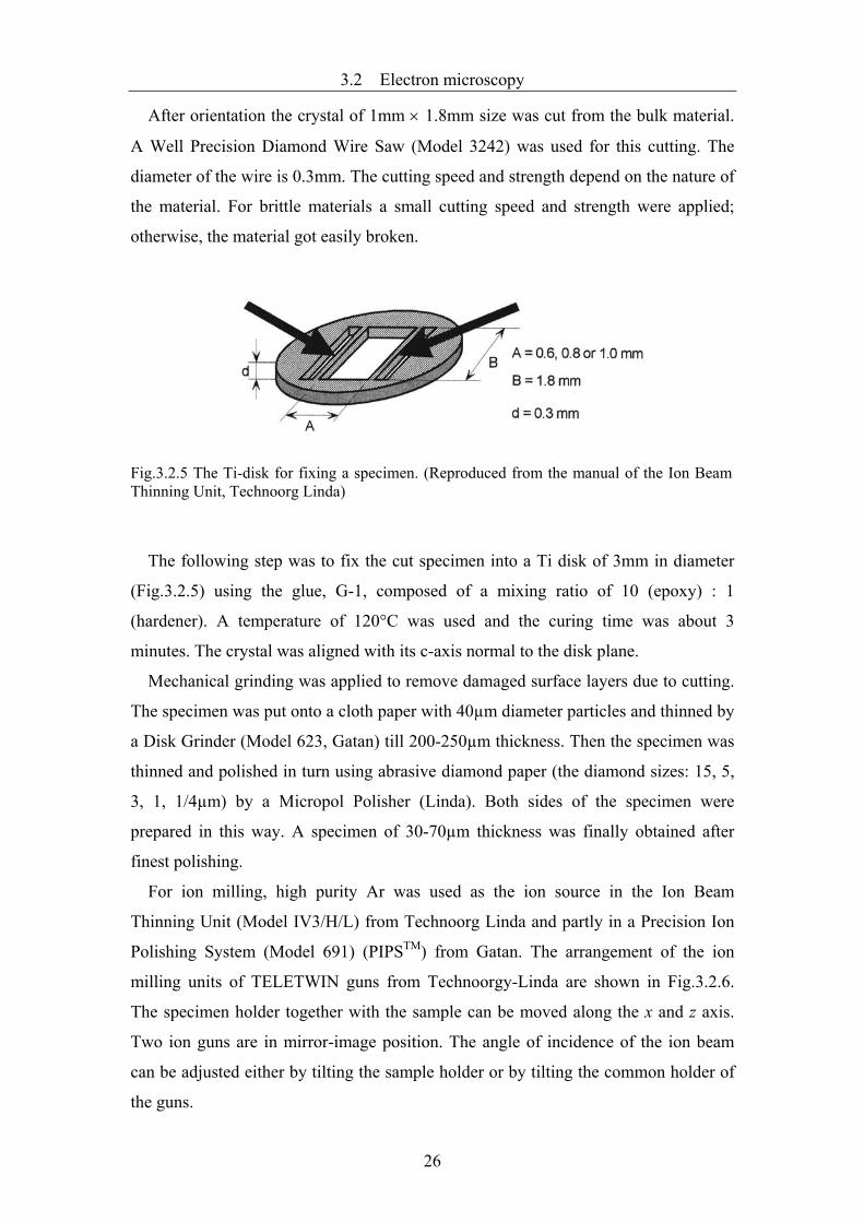
Fig.3.2.5 The Ti-disk for fixing a specimen. (Reproduced from the manual of the Ion Beam Thinning Unit, Technoorg Linda)
The following step was to fix the cut specimen into a Ti disk of 3mm in diameter
(Fig.3.2.5) using the glue, G-1, composed of a mixing ratio of 10 (epoxy) : 1
(hardener). A temperature of 120°C was used and the curing time was about 3
minutes. The crystal was aligned with its c-axis normal to the disk plane.
Mechanical grinding was applied to remove damaged surface layers due to cutting.
The specimen was put onto a cloth paper with 40µm diameter particles and thinned by
a Disk Grinder (Model 623, Gatan) till 200-250µm thickness. Then the specimen was
thinned and polished in turn using abrasive diamond paper (the diamond sizes: 15, 5,
3, 1, 1/4µm) by a Micropol Polisher (Linda). Both sides of the specimen were
prepared in this way. A specimen of 30-70µm thickness was finally obtained after
finest polishing.
For ion milling, high purity Ar was used as the ion source in the Ion Beam
Thinning Unit (Model IV3/H/L) from Technoorg Linda and partly in a Precision Ion
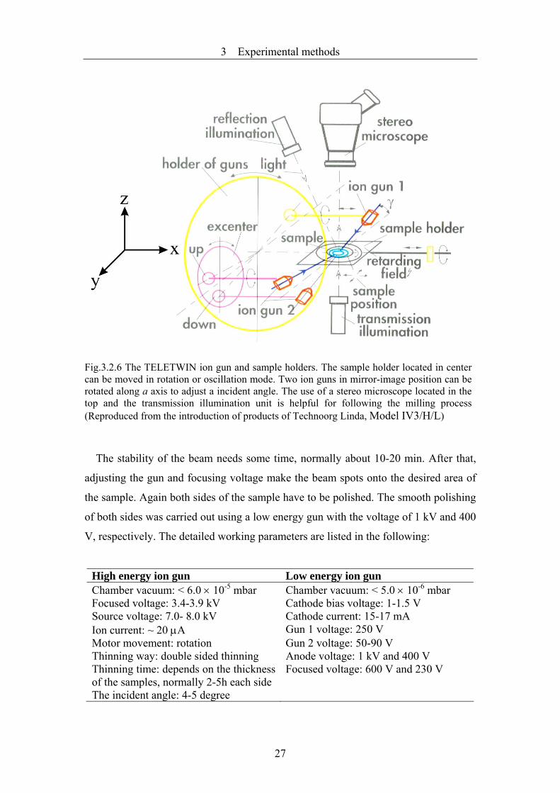
Polishing System (Model 691) (PIPSTM) from Gatan. The arrangement of the ion
milling units of TELETWIN guns from Technoorgy-Linda are shown in Fig.3.2.6.
The specimen holder together with the sample can be moved along the x and z axis.
Two ion guns are in mirror-image position. The angle of incidence of the ion beam
can be adjusted either by tilting the sample holder or by tilting the common holder of
the guns.
26
3 Experimental methods
Fig.3.2.6 The TELETWIN ion gun and sample holders. The sample holder located in center can be moved in rotation or oscillation mode. Two ion guns in mirror-image position can be rotated along a axis to adjust a incident angle. The use of a stereo microscope located in the top and the transmission illumination unit is helpful for following the milling process (Reproduced from the introduction of products of Technoorg Linda, Model IV3/H/L)
The stability of the beam needs some time, normally about 10-20 min. After that,
adjusting the gun and focusing voltage make the beam spots onto the desired area of
the sample. Again both sides of the sample have to be polished. The smooth polishing
of both sides was carried out using a low energy gun with the voltage of 1 kV and 400
V, respectively. The detailed working parameters are listed in the following:
High energy ion gun Low energy ion gun Chamber vacuum: < 6.0 × 10⁻⁵ mbar Chamber vacuum: < 5.0 × 10⁻⁶ mbar Focused voltage: 3.4-3.9 kV Cathode bias voltage: 1-1.5 V Source voltage: 7.0- 8.0 kV Cathode current: 15-17 mA Ion current: ~ 20 µA Gun 1 voltage: 250 V Motor movement: rotation Gun 2 voltage: 50-90 V Thinning way: double sided thinning Anode voltage: 1 kV and 400 V Thinning time: depends on the thickness of the samples, normally 2-5h each side
Focused voltage: 600 V and 230 V
The incident angle: 4-5 degree
27

3.2 Electron microscopy
The Precision Ion Polishing System (PIPS) was also used for the preparation of a
few specimens. The corresponding conditions are listed as follows:
αup 7° 5° 4° 4° 4° 2° αdown 7° 5° 4° 4° 4° 2°
Voltage (kV) 5 5 5 4 3 1.7 Time (min) 35 35 115 20 15 15
αup and αdown- the incident angle of the ion gun above and below the sample with respect tothe surface of the sample.
The PIPS with a small volume of the chamber easily reaches the final vacuum after
putting in or taking out the sample. During the whole process of preparation, the
incident angles of the two guns and the gun voltage were decreased step by step at a
rather good focus. The sample was thinned and polished on both sides at the same
time. The lowest voltage of the gun available is about 1.5 kV.
Comparing the two ion beam thinning units, the PIPS allows better to adjust the
incident angle and to control the beam focus, while the Technoorg-Linda apparatus
provides a higher quality surface of the sample because of the use of low energy gun.
Fig.3.2.7 shows a final sample prepared by the two techniques. The former has a very
good surface and the center hole indicates a good focus and alignment of two guns
(Fig.3.2.7a). The latter shows a irregular hole and relative rough surface (Fig.3.2.7b).
Fig.3.2.7 (a) a sample prepared by Technoorg-Linda apparatus showing the smooth surface; (b) a sample prepared by PIPS showing damaged surface.
28

3 Experimental methods
3.2.2 Scanning electron microscopy, energy-dispersive X-ray
spectrometry and wavelength-dispersive X-ray spectrometry
3.2.2.1 SEM
The principle function of SEM is to produce surface images of three-dimensional
objects. The most commonly used types of images are secondary electron (SE)
images, which show topographic features, and backscattered electron (BSE) images,
which are used to reveal compositional variations.
Secondary electrons with energies less than 50eV are emitted from the specimen
after collision with high energy incident electron beams. The emission of secondary
electrons is very sensitive to the angle at which the electron beam strikes the surface.
To a large extent, contrast in SE images arises from the variation of the angle between
the running direction of secondary electrons emitted from the specimen surface and
the detector.
Backscattered electrons are electrons from the incident beam which have interacted
with atoms in the specimen and reflected out again. Owing to their relatively high
energy comparable to the energy of the primary electrons, backscattered electrons
travel in almost straight lines. The amount of the BSE shows a dependence on the
angle between primary beam and specimen surface similar to that of the SE, so the
apparent brightness of those regions which can be ‘seen’ by the detector varies with
the angle between the surface and detector. The resulting effect gives a good
impression of the topography of the specimen. With the usual types of BSE detector
which are insensitive to low-energy electrons it is desirable to use an accelerating
voltage of 15kV or higher for BSE imaging.
3.2.2.2 EDS and WDS
The energy-dispersive (ED) type consists of a solid-state detector which produces
pulses proportional to X-ray photon energy, which are sorted electronically by their
amplitude in order to produce a spectrum. The pulses are processed in quick
succession and the whole spectrum is effectively recorded in ‘parallel’.
In ED spectrometers the X-ray detection medium is a semiconductor crystal
(usually silicon doped with Lithium which provides the formation of electron-hole
pairs) with an electronic band structure in which the valence band is normally fully
29

3.2 Electron microscopy
occupied by electrons. When an X-ray photon is absorbed it generates Auger and
photo-electrons, which dissipate their energy partly by raising valence electrons to the
conduction band. The arrival of each photon thus creates a brief pulse of current
caused by electrons and holes moving in opposite directions under the influence of the
bias voltage of the detector. The X-ray collection efficiency of an ED spectrometer
can be maximized by placing the detector as close as possible to the source. The
efficiency of detection of the X-rays reaching the detector is close to 100% over the
energy range of 2 ~ 20keV.
The wavelength-dispersive (WD) type makes use of Bragg reflection by a crystal.
X-rays are scattered by the atoms in the crystal similar to that of the electron. The
result causes the strong reflections where the Bragg equation is satisfied. The most
intense reflections (the first order n = 1) is normally used in WD analysis. The
wavelength range (for n = 1) is limited for a given value of d. Several detecting
crystals of different spacing are therefore needed to cover an appropriate range of
wavelengths. The crystals normally used are LiF (d = 2.013Å), PET (4.371Å) and
TAP (12.95Å). WD spectrometers operate in ‘serial’ mode and are turned to only one
wavelength at a time.
The comparison of ED and WD spectrometry is summarized in Table 3.2.1.
Table 3.2.1 Comparison of ED and WD spectrometry. ED WD Spectrum resolution Low (110-140eV) High (ca. 10eV) Signal-to-noise ratio Low (ca. 100) High (ca. 1000) Count rate/specimen current High/ca. 10-10 A Low/ca. 10-7 A
Detection method All elements at the same time One by one
Spectrum record simultaneous Sequential Analysis time Short Long Element range 5B-92U 4Be-92U Accuracy 2-10% 1-2%
3.2.2.3 Instrumentation further used
A CamScan 4 SEM equipped with a Thermo Noran detector was used for EDS
mapping and compositional analysis. Thin sections of as-grown crystals were cut and
polished for SEM measurements. The images using backscattered electrons or
secondary electrons were taken at 15kV accelerating voltage, respectively.
30

3 Experimental methods
A SX100 electron probe micro analyzer produced by CAMECA was used for high
precision quantitative analysis for some as-grown crystals. The back scatter images
and composition of the sample were measured using at 20kV accelerating voltage and
40.2nA beam current. The size of each measured spot was about 10 µm in diameter.
31

3.3 Electron spin resonance
3.3 Electron spin resonance
Electron Spin Resonance (ESR), also referred to as Electron Paramagnetic
Resonance (EPR), is concerned with the energy differences between allowed spin
states of an electron spin. An electron has a spin S = ½ and an associated magnetic
moment. In a magnetic field B two spin states S = +1/2 and S = -1/2 occur with
different energies (Fig.3.3.1).
Fig.3.3.1 Energy levels of a spin S = ½ in a magnetic field B. g is g-factor. βe is the Bohr magneton.
The energy difference for an electron spin, S, is in the microwave region and, hence,
transitions between the two spin states can be induced by applying a microwave
radiation to the sample within a magnetic field.
Normally, ESR spectra are obtained by keeping the microwave frequency fixed and
varying the magnetic field until the resonance is reached. At resonance, the energy
difference between the two states is given by
0BgE eβν ==∆ h (3.36)
where βe is the Bohr magneton (magnetic moment of a free electron), B is the applied
magnetic field, ν is the frequency and g is the so-called g-factor [45].
For an isolated free electron g = 2.0023. The g-factor is strictly a tensor and its
effective value may vary depending on the symmetry of the paramagnetic centre. In
single crystal studies the symmetry may be determined by observing the variation of
ESR transitions with changing orientation of the crystal relative to the magnetic field
B.
32

3 Experimental methods
ESR is very sensitive in detecting low spin concentrations, and the detection limit
can be as low as 1011 spins. Sensitivity is improved by keeping the sample at low
temperature (e. g. liquid helium temperature, 4.2K), which increases the population
difference between two energy states.
The description above refers to a single electron with two spin states +1/2 and -1/2.
However, transition metal ions and rare earth ions have more than one unpaired
electron i.e. S = n/2 where n is the number of unpaired electrons and 2S + 1 spin
energy levels occur in a magnetic field. Transitions within these 2S + 1 levels are
governed by the selection rule ∆S = ± 1, which results in a spectrum with 2S lines,
referred to as the fine structure in ESR.
In a spherically symmetric electric field, all of these 2S + 1 energy levels are
degenerate and the application of an external magnetic field B, splits the levels
equally, so only one line will be seen in the ESR spectrum. However, in a crystal the
electric field is generally distorted depending on the coordination of the paramagnetic
ion and, therefore, the effect of the unpaired electrons on each other depends on the
symmetry of the ligand field which produces a so called zero field splitting of the
energy levels. Hence, resonance does not occur at the same value of the applied field
B but at different values of B. Therefore, more than one line will be seen in the ESR
spectrum.
ESR spectroscopy is a very sensitive tool for detecting paramagnetic centres in
small concentration. The spectrum can provide information about the local structural
and electronic environment of the paramagnetic centre e.g. Cr3+, Co2+ etc. This can be
applied to a wide variety of problems either in directly studying the local structure or
in using the paramagnetic centre as a probe to monitor processes and reaction in
minerals. In addition, ESR technique may be used to determine the site occupied by
elements with unpaired electrons, the oxidation state of an element, change in local
structure etc.
33

3.4 X-ray diffraction
3.4 X-ray diffraction
X-rays are high frequency (~ 1018Hz) electromagnetic waves. The oscillating
electric field of X-rays interacts with the electrons of an atom, causing them to
oscillate with the same frequency. In general, heavy atoms scatter more strongly
electrons than light atoms. This proportionality would only be a simple one if the size
of atoms is small relative to the X-ray wavelength. However, heavy atoms have
dimensions of the same order as the X-ray wavelength. The effect of this is that X-
rays scattered from different points in the electron cloud of the same atom interfere
with one another resulting in a fall-off in the scattered intensity with the angle through
which the incident beam has been scattered. At small scattering angles the scattering
is proportional to the atomic number.
When X-rays pass through a crystal the diffraction wave conform to the Bragg
equation, that is, the diffractions from a row of lattice points occur at distinct angles
and interfere each other when their path differences are integral number of
wavelengths. Figure 3.4.1 shows the diffraction geometry. An incident beam is
diffracted from two successive (hkl) planes with interplanar spacing dhkl. The path
difference for beams from successive planes is given by AB + BC = 2dhkl sinθ and,
hence, the condition for diffraction maxima is
λθ ndhkl =sin2 (3.4.1).
Fig.3.4.1 The condition for Bragg reflection from planes (hkl) with spacing dhkl. The path difference between X-rays reflected from successive planes is AB + BC.
The most common application of the Bragg equation is in the interpretation of X-
ray diffraction pattern from powders. X-ray powder diffraction is a standard method
for identifying crystalline materials, determining their lattice parameters, and in some
cases determining crystal structures from the diffracted intensities.
34
3 Experimental methods
A Siemens DIFFRAC-500 diffractometer with a Cu-Kα radiation (λ = 0.15406nm,
Ni filter, sample pressed onto glass plates) and a Philips X`Pert MRD (θ-θ geometry,
samples on Si single crystal sample holder, secondary monochromator, point detector)
with CuKα radiation (Si as an external standard) was used for phase identification.
The scanning range of 10° ≤ 2θ ≤ 80° is used with the scanning steps of 0.03°. The
measured results are compared with the corresponding data from inorganic crystal
structure data (ICSD) using PowderCell program.
An imaging plate diffraction system (STOE IPDS-II) using graphite-
monochromatized Mo Kα radiation was used for collecting single crystal data. An
Oxford cryosystem device which can be cooled down to 100K was used for
investigations of the phase transition.
35

3.5 Magnetic measurements
3.5 Magnetic measurements
Magnetic moments associated with atoms in magnetic materials have three origins:
These are the electron spins, the electron orbital motion and the change in orbital
motion of the electrons caused by an applied magnetic field H.
The diamagnets are solids with no permanent net magnetic moment per atom.
Diamagnetic susceptibility χ arises from the realignment of electron orbital under the
action of a magnetic field. Therefore all materials exhibit a diamagnetic susceptibility,
although not all are classified as diamagnets. Some materials have a net magnetic
moment per atom, due to an unpaired electron spin in each atom which leads to
paramagnetism or even to ordered magnetic states such as ferromagnetism and
antiferromagnetism. In each case the paramagnetic or ferromagnetic susceptibility is
much greater than the diamagnetic susceptibility and therefore is the dominant effect.
Paramagnetism occurs at higher temperatures in all materials which have a net
magnetic moment. The atomic magnetic moments are randomly oriented but can be
aligned by a magnetic field.
Only the change in orbital motion gives rise to a diamagnetic susceptibility.
Diamagnetism leads to a very weak magnetization which opposes the applied
magnetic field. The diamagnetic susceptibility is therefore negative and has an order
of magnitude of -χ ≈ 10-5 or 10-6. It is also found to be independent of temperature.
Both the electron spin and the orbital angular momentum contribute to the
magnetization which leads to positive susceptibility. The susceptibilities of
paramagnets are typically of the order of χ ≈ 10-3 to 10-5, and at low fields H the
magnetization M is proportional to H. The susceptibilities of a large number of
paramagnetic solids were measured over a wide temperature range. It is found that the
susceptibility varies inversely with temperature,
TC
=χ (3.5.1)
where C is the Curie constant. The materials obeying this law are materials in
which the magnetic moments are localized at the atomic sites, i.e. the magnetic atoms
are surrounded by a number of non-magnetic atoms. But it was also found that for the
description of χ (T) a more generalized form is necessary known as the Curie-Weiss
law:
36

3 Experimental methods
)( pTCθ
χ−
= (3.5.2)
where θp is the paramagnetic Curie temperature. θp can be either positive, negative or
zero. For materials that undergo a paramagnetic to ferromagnetic transition θp > 0
corresponds to the Curie temperature TC. For materials that undergo a paramagnetic to
antiferromagnetic transition the term θp is less than zero (θp < 0), although in practice
the transition temperature between the paramagnetic and antiferromagnetic phases
occurs at a positive temperature TN known as the Neel temperature. It should be
remembered that the susceptibility only follows the Curie-Weiss law in the
paramagnetic region. As soon as the material becomes ordered the susceptibility
behaves in a very complicated way and no longer has a unique value for a given field
strength.
There are a number of different types of magnetic order in solids including
ferromagnetism, antiferromagnetism, weak ferromagnetism ferrimagnetism and
helimagnetism. Rare earth compounds, for example, exhibit more than one ordered
magnetic state. These ordered states undergo transitions at critical temperatures so
that every solid that exhibits one of these types of magnetic order will become
paramagnetic at higher temperatures. For example in a ferromagnet, e.g. Fe, Co, Ni
with strong exchange interactions between the magnetic dipoles, the Curie point is the
transition temperature above which the material becomes paramagnetic and below
which an ordered ferromagnetic state exists. The Neel point is the temperature below
which an ordered antiferromagnetic state exists. Some solids such as terbium,
dysprosium and holmium have both Curie and Neel temperatures. Fig.3.5.1 shows
some possible types of magnetic ordering of solids.
In oxides a different kind of exchange interaction occurs via the oxygen atoms, and
the spins of neighbouring metal ions become aligned in an antiparallel way. This
coupling mechanism, e.g. Fe (↑) – O – Fe (↓), is termed as superexchange interactions,
and becomes most effective as the Fe – O – Fe bond angle approaches 180°. If the
moments are exactly antiparallel, there is no net magnetic moment. In some cases the
spin directions are not precisely antiparallel and a small net magnetic moment results
from this spin canting.
37

3.5 Magnetic measurements
Fig.3.5.1 Different types of magnetic ordering
Hematite (Fe2O3) is a famous example for a canted antiferromagnet with a Curie
temperature of 680°C. Silicate minerals containing paramagnetic ions only become
magnetically ordered at low temperatures and therefore they do not play a role in the
magnetism of rocks. But none the less a lot of silicates can stand for model substances.
The Quantum Design Magnetic Properties Measurement System (MPMS-2) is a
SQUID-magnetometer allowing highly automated measurements of the magnetic
moment of a wide variety of samples as a function of magnetic field, temperature or
time. Magnetic moments down to 10-7emu (10-7Gcm3) can be measured in a
reproducible way. The MPMS has a temperature range between 1.8K and 400K, the
superconducting magnet can reach magnetic fields between -5.5Tesla and +5.5Tesla.
Specimens must be fixed rigidly inside a tube which is magnetically homogeneous
and of low magnetic susceptibility. For experiments in the temperature range 2K-
330K, we use transparent drinking straws.
The background signal contributed by the mount can be recorded separately and
subtracted from the data. Fields are applied parallel to the specimen tube, and the
magnetisation of the specimen is measured along the same direction.
38

3.6 Other methods
3.6 Other methods
Besides the techniques outlined in some detail above the following experimental
techniques have also been used to characterize and investigate the samples.
3.6.1 Differential scanning calorimeter
A Mettler Toledo DSC 821e was used for the investigation of the anomaly of heat
capacity in the selected system under nitrogen atmosphere. The sample was placed in
a standard aluminum pan. The sample amount was 7mg. The cycle of heating and
cooling at a rate of 5K /min was carried out twice. The second heating curve was used
to calculate the phase transition temperature. Temperature and enthalpy were
calibrated with ultra-pure zinc- and indium-sample.
3.6.2 Photoluminescence measurements
A Perkin-Elmer Lamda 9 with a spectral resolution of about 2nm was used for the
measurements of the excitation and emission spectra. The setup was equipped with a
Xe lamp of 1000W as heat source and two monochromators (spectropro 300I, Acton
Research, Polytec) controlled by a NCL single-channel spectroscopy detection system.
A Shimadzu RF-1502 spectrofluorometer (light source = XBO lamp) with a
resolution of about 15nm was also used. The light power at the excitation wavelength
was in the range below 1mW.
39

4.1 Synthesis of Ca2MgSi2O7, Ca2CoCoSi2O7 and Ca2ZnSi2O7 melilites
4 Results and discussions
4.1 Synthesis of Ca2MgSi2O7, Ca2CoSi2O7 and Ca2ZnSi2O7 melilites
Powder of high purity of CaCO3 (99.97%, Merck), of MgO (99.999%, Ventron
GMBH), of Co3O4 (99.7%, Merck), of ZnO (99.999%, Merck) and of SiO2 (99.995%,
Merck) were weighed in stoichiometric proportions. MgO was first heated at 1000°C
for 5h to remove absorbing water. The stoichiometric mixture was then ground in an
agate mortar, pressed into pellets and calcined in a program-controlled oven. The
calcined powder was mixed again and sintered until the pure intended compound was
obtained. The whole preparation procedure is given in scheme 4.1.1.
Raw materials
XRD Final Weigh Grind Press Sinter measurement compounds
Repeat
Scheme 4.1.1 The procedure of preparing powder material.
The reaction equations for the three compounds are given as follows:
CaMg-åkermanite
2 CaCO3 + 1 MgO + 2 SiO2 → 1 Ca2MgSi2O7 + 2 CO2 ↑
CaCo-åkermanite
12 CaCO3 + 2 Co3O4 + 12 SiO2 → 6 Ca2CoSi2O7 + 12 CO2 ↑ + O2 ↑
CaZn-åkermanite
2 CaCO3 + 1 ZnO + 2 SiO2 → 1 Ca2ZnSi2O7 + 2 CO2 ↑
The reaction process involves the decomposition of CaCO3 when the temperature is
higher than about 900°C [46] according to:
T > 900°CCaCO3 CaO + CO2 ↑
For the CaCo-åkermanite synthesis, it also involves the decomposition of Co3O4 into
CoO and O2 according to:
40

4 Results and discussions
Taking into account the decomposition of CaCO3 and Co3O4, the sintering program
of four steps was taken (Table 4.1.1). Step1 was to preheat the oven and step 2 for
decomposition. The raw materials reaction to form the expected product was
performed in step 3, which should use a low heat rate. Step 4 was to drop temperature.
Table 4.1.1 Sintering program for three melilite systems.
Steps Heat rate (°C/h)
Final Temp. (°C)
Dwell time (h) Notes
1 800 200 0 System requirement
2 200 1000 2 In order to decompose CaCO3 and Co3O4
3 75 1350/1200/1300 48 CaMg- / CaCo- / /CaZn-åkermanite
4 -150 50 0 Temperature drop
After the first sintering, XRD results of the end-member of Ca2MgSi2O7 show that
the main phase is Ca2MgSi2O7. Some additional peaks correspond to Ca3MgSi2O8 and
CaMgSi2O6. The pure phase of Ca2MgSi2O7 could be achieved after a third sintering
process (Fig.4.1.1).
10 20 30 40 50 60 70 80
0
1000
2000
3000
4000
5000
6000
7000
c
b
a
Inte
nsity
(cps
)
2θ
For the end-member Ca2CoSi2O7 a longer reaction time was needed to obtain the
pure phase. The possible reason is due to the use of Co3O4. In the intended product Co
2 Co3O4T > 950°C 6 CoO + O2 ↑.
Fig.4.1.1 XRD diagrams of Ca2MgSi2O7. a) after first sintering run; b) after third sintering run; c) data from ICSD-100736.
41

4.1 Synthesis of Ca2MgSi2O7, Ca2CoCoSi2O7 and Ca2ZnSi2O7 melilites
exists in the valence state 2+. Although Co3O4 starts to decompose at about 950°C,
the complete decomposition process is rather slow, which is confirmed by the color
change of the sample from grey-black to deep blue. After repeating the sintering five
times the pure phase was obtained as identified by XRD in Fig.4.1.2.
20 30 40 50-1000
0
1000
2000
3000
4000
5000
6000
d
c
b
a
Inte
nsity
(cps
)
2θ
Fig.4.1.2 XRD diagram of Ca2CoSi2O7. a), b) and c) corresponding to first, third and five sintering runs, respectively; d) data from ICSD-72543.
For the end-member Ca2ZnSi2O7 the experiments showed that it is very difficult to
get the pure phase comparing to the former two. The stoichiometric raw materials
were calcined three times, however, four additional peaks were always observed in
the XRD diagrams. Refinement of the measurements using PowderCell program [47]
showed that these additional peaks belong to Ca3Si3O9-26553 from inorganic crystal
structure database (ICSD), which are obviously formed because of the evaporation of
ZnO during the high-temperature reaction process. The refinement results showed that
approximate 88% Ca2ZnSi2O7 and 12% Ca3Si3O9 were obtained. Therefore, 5/4 of
stoichiometric ZnO was added to the mixture and sintered again. The XRD results
then showed a good agreement with the single-crystal data of Ca2ZnSi2O7-18114
(Fig.4.1.3).
42

4 Results and discussions
20 30 40 50-1000
0
1000
2000
3000
4000
5000
6000
b
c
d
a
Inte
nsity
(cps
)
2θ
Fig.4.1.3 XRD diagram of Ca2ZnSi2O7 powder. a) after fourth sintering (additional ZnO); b) after third sintering; c) and d) the data of Ca3Si3O9 and Ca2ZnSi2O7 from ICSD, respectively.
43

4.2 Single crystal growth
4.2 Single crystal growth
For the growth of melilite crystal two main methods, the Czochralski (CZ) [48] and
the Floating Zone (FZ) melting [49] method, were reported. In the present work, all
single crystals were grown by the FZ melting method.
In this section, the preparations for single crystal growth, the growth parameters,
and the particular growth procedure for each system were described. The growing
steps responsible for the final crystal quality were outlined.
4.2.1 The preparation of a feed rod and a seed crystal
The preparation of the feed rod is crucial for a successful growth process. After
powder synthesis of the end-member compounds, melilites with different composition
were obtained by proportionally mixing two end-members. The mixtures then were
prepared into rods with certain diameter and length.
Normally, there are two ways to prepare a rod. One is that the powder is intimately
mixed together with acetone in a polyethylene blender, placed into a sealed rubber
tube to form a rod, and then hydrostatically pressed. Finally, the rod is calcined at a
certain temperature.
Another way is to place the powder into an alumina tube where it is calcined,
subsequently. We used the latter way to prepare rods of 4 mm diameter and 40-60 mm
length. A small quantity of the powder was given into the alumina tube and
immediately compressed by hand using a quartz stick. Then the next powder load was
added and compressed and so on. If too much powder was added at once, the rod can
break easily. The procedure is illustrated in Fig.4.2.1.
For the series Ca2MgSi2O7-Ca2ZnSi2O7, excess of 1% ZnO related to the amount of
the Ca2ZnSi2O7 as well as a small amount of Ca2CoSi2O7 was added into the rod. The
ZnO excess compensates the loss of evaporation during sintering and growing, while
Ca2CoSi2O7 increases the absorption of radiative energy by changing the rod color
from white to light blue. The experiments proved that the Ca2CoSi2O7 excess
decreased the input energy efficiently. The temperature for sintering was the same as
that of synthetic powder.
44

4 Results and discussions
Fig.4.2.1 (a) The preparation of a rod in an Al2O3 tube; (b) the centered rod of Ca2Co0.7Zn0.3Si2O7 used for crystal growth.
A seed crystal is necessary to grow single crystals. There are three advantages for
using a seed crystal:
- Crystals with a certain orientation can be grown by a pre-oriented seed crystal;
- Nucleation happens only on boundaries of a seed crystal;
- A stable growth interface can be reached easily.
To grow a seed crystal the following steps were performed:
1) The sintered rod, fixed into a ceramic tube located in the upper shaft of the
pulling unit, was used as nutrient. A Pt wire of 0.5mm diameter was mounted
into a ceramic rod of the lower shaft.
2) The rod and the Pt tip were centered along the rotating axis and counter-
rotated with a certain speed to ensure a flat interface and homogeneity.
3) The nutrient rod was moved into the focus area of the lamps and the input
power was increased step by step until the rod starts to melt.
4) When the material in the zone was melted homogeneously, the Pt tip was
moved upwards until the hanging melting drop was touched.
45

4.2 Single crystal growth
5) After the equilibrium was achieved, the Pt tip was pulled down carefully until
the solid-liquid interface could be observed.
6) The growing speed and the traveling-down speed of the feed rod could be set
at this time.
7) At the end of the growth procedure, the temperature was lowered slowly to
reduce the volume of the melting zone. Finally the as-grown crystal was
separated from the melt.
Because the as-grown crystal using a Pt tip is arbitrarily oriented a orientation of
the crystal has to be carried out, before a parallelepiped of 2 × 2 × 5mm3 size for the
use as seed crystal can be prepared.
4.2.2 Growth of Ca2Mg1-xZnxSi2O7, Ca2Co1-xZnxSi2O7, (Ca1-xSrx)2CoSi2O7
crystals
Generally, the growth of a high-quality crystal requires maintaining the growth
conditions as stable as possible. Fig.4.2.2 shows the four stages of the growth process.
The initial amount of the melt has a strong influence on the subsequent formation of
the solid-liquid interface and its position. Too much melt moves the solid-liquid
interface downwards even under the same input voltage. The increase of the melt
volume is especially disadvantageous for crystal growth when evaporating material
like ZnO is present. In addition, if the melting point of the seed crystal is a little bit
higher than that of the rod (for example, the seed crystal of Ca2Co0.7Zn0.3Si2O7 was
used for growing the Ca2Co0.9Zn0.1Si2O7 crystal), the seed crystal will be covered by
the melt and finally melted completely due to the heat capacity and conductivity if
there is an excess of the melt.
To obtain a suitable volume of the melt, one should first try to get a rough value of
the input voltage under which the rod can be melted. Then the input voltage must be
adjusted carefully. This step takes some time because the effect of the input voltage
on the rod can be detected after a certain time. Three different situations of the melt
are shown in Fig.4.2.3.
46

4 Results and discussions
Fig.4.2.2 The four stages of the FZ growing process. R – Rod; MZ – Melting zone; I – Solid-liquid interface; SC – Seed crystal. a) the melting rod (R) and the seed crystal (SC); b) contact between rod and seed crystal; c) crystal growth at the beginning with smaller diameter; d) crystal growth under fixed conditions.
Fig.4.2.3 Three possible melting shapes of the melt drop. The volume of the melt is indicated roughly by the white arrow. a) too less; b) just right; c) too much.
47

4.2 Single crystal growth
The suitable volume of the melt should be just a little bit larger than a half sphere
zone in place is the surface tension, it is possible to obtain the quantitative expression
by
whose radius is the same as that of the rod. Because the major force holding a floating
neglecting the cohesion between the solid and liquid and buoyancy. The growth
angle is often used for the description of the melt shape (or volume), which is defined
as the angle α between the meniscus surface and the growth direction of the crystal at
the solid-liquid-gas trijunction (Fig.4.2.4). More information can be referred to the
corresponding literatures [50].
touched the melt. To get the solid-liquid interface, one may drag the seed crystal
ownwards, and meanwhile, sometimes adjust the input voltage. In fact, careful
co
Fig.4.2.4 Growth angle α. Important parameters controlling the floating zone process: σlg, σsb, nd σsg are the interface free energies liquid-gas, solid-liquid and solid-gas, respectively. a
Once the melt was homogeneous, the seed crystal was moved upwards until it
d
ntrol of the melt volume as well as of the temperature gradient is important to attain
a stable solid-liquid interface. Fortunately, the situation of the interface can be
observed directly on the monitor by means of a CCD camera. In Fig.4.2.5 a good and
stable solid-liquid interface is shown.
48

4 Results and discussions
Fig.4.2.5 Picture taken at stable condition during growing crystal process. A stable and plane solid-liquid interface can be seen clearly.
The suitable traveling-down speed (growth speed) can be set up after obtaining the
sta
fro
growing condition with less oxygen pressure.
ble solid-liquid interface. For our experiments, a traveling-down speed of 1.0 mm/h
of the seed crystal was normally used. However, at the beginning, often a speed of 0.5
mm/h of the rod was used, leading to a smaller diameter of the as-grown crystal which
benefits to grow single crystal. Although the seed crystal with certain lattice facets
was used, growth of the crystal may occur in different directions at the beginning.
Therefore, the diameter of the crystal should be as small as possible to decrease the
number of nucleation possibilities. Furthermore, different growth directions would
compete with each other until the dominant direction was obtained as described in
Fig.4.2.6. After that, the traveling-down speed of the rod can be increased to grow the
crystal with a larger diameter. It should be noted that the separation of the crystal
from the melt is also an important step. If the cooling procedure is too fast, it will
cause the formation of cracks within the grown crystal (see 4.3) which will be
discussed in more detail later. Normally we reduced the input voltage by 0.1 V/min.
For the melilite rod, a little gas could be absorbed into the melting zone, as seen
m Fig.4.2.7, which would be influential for heat convection and further, for the
crystal quality. This effect can be weakened by quenching the melt or by using
49

4.2 Single crystal growth
Fig.4.2.6 The crystal growth with different growing direction. (a-c) the evolution from multi- to single-growing direction. d) the crystal shape.
Fig.4.2.7 The melt hanging on the rod. A large bubble inside near the solid-liquid interface can be seen.
In the floating zone melting method, to grow a crystal one can also fix a seed
rystal onto the upper shaft and move it upwards. However, such as-grown crystals
no
cross-section of a crystal grown at the speed of 1.5 mm/h (Fig.4.2.8).
c
rmally include bubbles, therefore, we have chosen the moving-down technique. On
the other hand, when the seed crystal is fixed in the lower shaft oxygen bubbles are
introduced if the growing speed is too high, for example, bubbles were observed in a
50

4 Results and discussions
he feed rods of Ca2Mg1-xZnxSi2O7 have white color. A white rod reflects the
radiative energy coming from halogen lamp more than a colored rod. Therefore, the
e increased to melt the rod, which may result in an overheating of
th
ermore, the instability of the solid-liquid interface. Under this growth
condition some cracks in the final crystal were observed. To solve this problem, one
Fig.4.2.8 Cross section of as-grown crystal at the speed of 1.5 mm/h. Dark circle dot representing bubbles.
Generally, each system required special growth conditions as described in the
following subparts.
Ca2Mg1-xZnxSi2O7
T
input power had to b
e rod. Further, ZnO easily evaporates at higher temperatures, therefore, overheating
must be avoided as much as possible. To solve this problem, 0.1 wt % Ca2CoSi2O7 of
deep blue color was added to the series Ca2Mg1-xZnxSi2O7. The acquired rods are light
blue and were sintered at 1350°C for 6h. The detailed conditions for growth are listed
in Table 4.2.1.
There was another problem during the growing process. The contamination of the
internal wall of the quartz tube by evaporating ZnO caused the loss of radiative
energy, and furth
51

4.2 Single crystal growth
had to use a small melt volume, which will be described in 4.4. Prolonging the
growing time, the loss of radiative energy was quite serious, so one had to keep the
temperature of the melting zone stable by increasing the input voltage or moving the
quartz tube. In the latter case, we could not grow long crystals because of the
limitation of the length of the quartz tube.
Table 4.2.1 Data of rods and as-grown crystals for the Ca2Mg1-xZnxSi2O7 system. Rods Crystals
Length Diameter Melting voltage
Growth Upper Lower Crystal voltage speed speed length x value
(mm) (mm) (V) (V) (mm/h) (mm/h) (mm)
0.0 37 87 73.3-73.5 0.5-1.0 1.0 4.7 23 0.1 36 7 4.8 87 3.6-73.9 0.5/1.2 1.0 9 0.3 34 4.6 88 7 3.4-74.2 0.5-1.2 1.0 10 0.5 32 4.6 7 77 3.8-74.9 0.5/1.0 1.0 11 0.7 69 .4 31 4.6 77 .0-70 0.7 1.0 10 0.9 30 4.6 75 72.2 0.5 1.0 7 1.0 32 4.6 62 66.7-67.0 0.7 1.0 14
Ca2 ZnxSi
A ds of 2 1-xZ x 2O7 so olut ue, t absorb the ra ve
nergy very well. Comparing to the rod of Ca2Mg1-xZnxSi2O7, the Ca2Co1-xZnxSi2O7
rod could be melted at a relatively low input voltage. The voltage to melt the rod was
that to keep a stable growth. The preparing method for rods was
th
Co1-x 2O7
ll ro Ca Co n Si lid s ions are bl hus ing diati
e
nearly the same as
e same as described above. For the solid solutions including Zn an excess of 1 wt %
ZnO was added. Because the difference of the melting points between the end-
members of Ca2CoSi2O7 and Ca2ZnSi2O7 is more than 100°C, the temperature for
sintering the rod was divided into two levels according to the ratio of Zn in the solid
solutions. Table 4.2.2 summarizes the details of the rod as well as the conditions for
growing crystals. The as-grown crystals are dark blue except that of the end-member
Ca2ZnSi2O7 (light blue). The crystals are free of bubbles, however, some cracks could
be observed at x > 0.7. The number of cracks increased with prolonging the growing
time. Evaporation of ZnO still exists during the whole growing process, but is much
smaller in comparison to the Ca2Mg1-xZnxSi2O7 system.
52
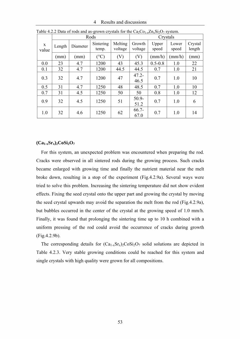
4 Results and discussions
Table 4.2.2 Data of rods and as-grown crystals for the Ca2Co1-xZnxSi2O7 system. Rods Crystals
Length Diameter Sintering temp.
Melting voltage
Growth voltage
Upper Lower Crystal speed speed length
x value
(mm) (mm) (°C) (V) (V) (mm/h) (mm/h) (mm) 0.0 23 4.7 1200 43 45.3 0.5-0.8 1.0 22 0.1 32 4.7 200 44.5 44.5 0. 0 21 1 7 1.
0 .3 32 4.7 1200 47 47.2-46.5 0.7 1.0 10
0.5 31 4.7 1250 48 48.5 0.7 1.0 10 0.7 31 4.5 1250 50 50 0.8 1.0 12
0.9 32 4.5 1250 51 50.9-51.2 0.7 1.0 6
1.0 32 4.6 1250 62 66.7-67.0 0.7 1.0 14
(C rx)2 i2O7
For this system, an unexpected problem was enc
racks were observed in all sintered rods during the growing process. Such cracks
became enlarged with growing time and finally the nutrient material near the melt
g in a stop of the experiment (Fig.4.2.9a). Several ways were
tri
a1-xS CoS
ountered when preparing the rod.
C
broke down, resultin
ed to solve this problem. Increasing the sintering temperature did not show evident
effects. Fixing the seed crystal onto the upper part and growing the crystal by moving
the seed crystal upwards may avoid the separation the melt from the rod (Fig.4.2.9a),
but bubbles occurred in the center of the crystal at the growing speed of 1.0 mm/h.
Finally, it was found that prolonging the sintering time up to 10 h combined with a
uniform pressing of the rod could avoid the occurrence of cracks during growth
(Fig.4.2.9b).
The corresponding details for (Ca1-xSrx)2CoSi2O7 solid solutions are depicted in
Table 4.2.3. Very stable growing conditions could be reached for this system and
single crystals with high quality were grown for all compositions.
53

4.2 Single crystal growth
Fig.4.2.9 a) The rod sintering 6 h at 1250°C showing the crack during the growing process; b) there are no cracks in the rod sintering 10 h or more at the same temperature.
Table 4.2.3 Data of rods and as-grown crystals for the (Ca1-xSrx)2CoSi2O7 system. Rods Crystals
Length Diameter Melting voltage
Growth voltage
Upper speed
Lower speed
Crystal length x value
(mm) (mm) (V) (V) (mm/h) (mm/h) (mm) 0.0 23 4.7 43 45.3 0.5-0.8 1.0 22 0.07 18 4.6 40.5 40.6 0.5-0.7 1.0 25 0.1 21 4.7 42 41 0.5-0.65 1.0 21 0.12 30 4.6 45 45.1 0.7-1.0 1.0 10 0.25 20 4.7 42 42 0.6 1.0 24 0.30 25 4.5 42.2 42.2 0.5-0.7 1.0 22 0.35 38 4.7 41.5 42 0.2-0.7 1.0 23 0.50 17 4.8 46.4 48.2 0.5-0.8 0.7 12 0.75 32 4.6 54 54.6 0.8 1.0 7
54

4 Results and discussions
4.3 Investigations of Ca2Mg1-x(Zn, Co)xSi2O7 with modulated
structure
This section includes two series melilites. The crystal characterization and the
incommensurate-to-normal phase transition were described in Ca2Mg1-xZnxSi2O7.
Studies of the structural modulation of Ca2Mg1-xCoxSi2O7 by means of TEM were
reported. Detailed growth conditions and the corresponding characterization can be
found in Pokoj’s diploma work [51].
4.3.1 The Ca2Mg1-xZnxSi2O7 system
4.3.1.1 Crystal characterization
A series of Ca2Mg1-xZnxSi2O7 single crystals with the nominal values x = 0, 0.1, 0.3,
0.5, 0.7, 0.9, 1.0 were grown using the floating zone melting method. Fig.4.3.1 shows
two as-grown crystals of different Zn concentration. Usually, at lower Zn
concentration crystals of high-quality were obtained. With increasing Zn/(Mg + Zn)
ratio, cracks were observed at the surface of the crystals. The number of cracks
increased with increasing Zn content and growth time. The main reason for that is the
evaporation of Zn at high melting temperatures. The evaporation of Zn causes an
unbalance of the composition and instability of the solid-liquid interface, yielding
atomic micro-arrangements of atoms inside the interface may occur with different
crystallographic orientations. Hence, the amount of Zn was kept as constant as
possible during the experiments (see 4.2).
(b) (a)
Fig.4.3.1 As-grown crystal of Ca2Mg0.9Zn0.1Si2O7 (a) and Ca2Mg0.3Zn0.7Si2O7 (b). The light blue color crystals correspond to a length of ca.10 mm.
55

4.3 Investigations of Ca2Mg1-x(Zn, Co)xSi2O7 with modulated structure
Besides these factors, the quality of the seed crystal is also important. Two different
seed crystals were used for growing the end member Ca2MgSi2O7. One seed crystal,
grown by pulling a Pt wire from the melt, had several cracks, the other was of good
quality with the crystallographic c axis parallel to the growing direction.
The crystal grown by the “cracked” seed crystal has cracks inside (Fig.4.3.2a).
However, the crystal grown by the second seed crystal has no cracks (Fig.4.3.2b).
Both as-grown crystals were free of bubbles and inclusions. On top of the crystal in
Fig.4.3.2a, the evident crack marked by arrow is due to the fast cooling speed after
finishing the growth. Therefore, always the lowest cooling speed of 1°/ min attainable
by the cooling system has been used. The crystal length is ca. 10 mm.
Fig.4.3.2 As-grown crystals of Ca2MgSi2O7 using the seed crystals with different quality. (a) the seed crystal with some cracks grown by Pt wire as seed crystal; (b) the seed crystal of Ca2MgSi2O7 with good quality and the crystallographic c axis paralleling to a growing direction
Thin polished sections cut from the bulk crystals were used for the SEM-EDS
compositional analysis. The calculated results based on the EDS measurements are
listed in Table 4.3.1. The measured concentrations of Zn are less than the
corresponding nominal values. The difference between the nominal and the measured
concentration of Zn increases with increasing Zn content of the raw material. This
implies that there is still an evident evaporation of Zn despite the above-mentioned
precautions.
56
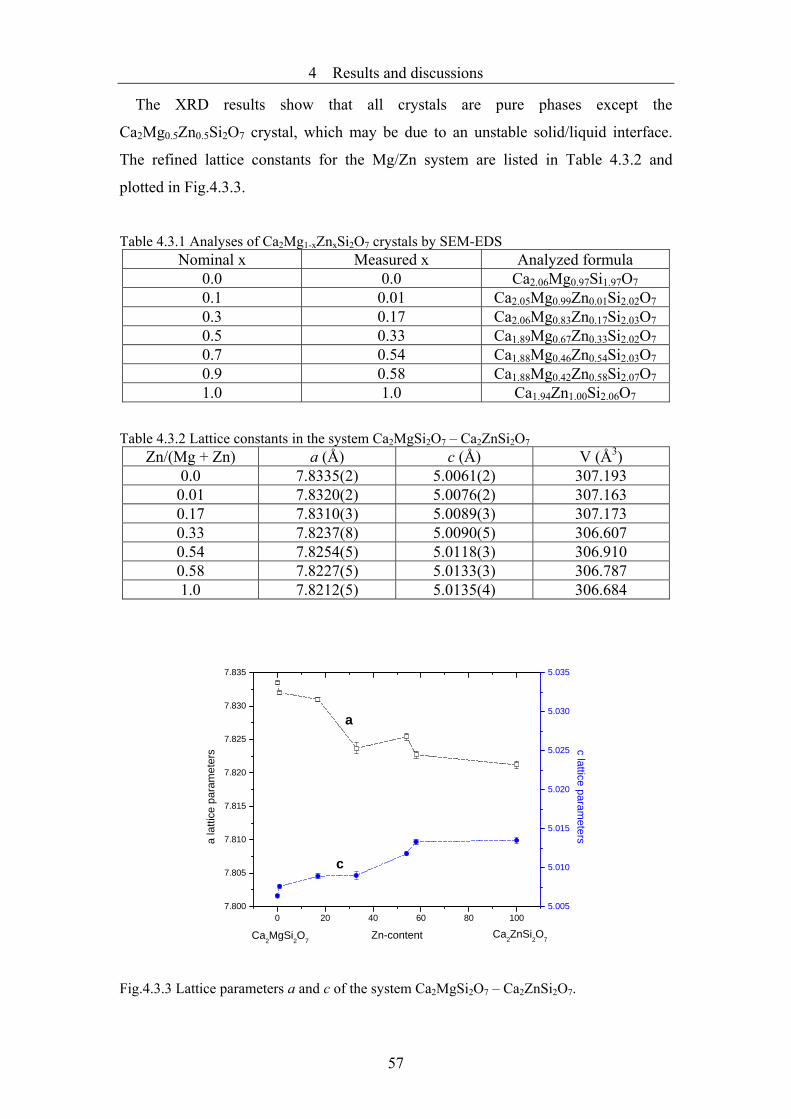
4 Results and discussions
The XRD results show that all crystals are pure phases except the
Ca2Mg0.5Zn0.5Si2O7 crystal, which may be due to an unstable solid/liquid interface.
The refined lattice constants for the Mg/Zn system are listed in Table 4.3.2 and
plotted in Fig.4.3.3.
Table 4.3.1 Analyses of Ca2Mg1-xZnxSi2O7 crystals by SEM-EDS Nominal x Measured x Analyzed formula
0.0 0.0 Ca2.06Mg0.97Si1.97O70.1 0.01 Ca2.05Mg0.99Zn0.01Si2.02O70.3 0.17 Ca2.06Mg0.83Zn0.17Si2.03O70.5 0.33 Ca1.89Mg0.67Zn0.33Si2.02O70.7 0.54 Ca1.88Mg0.46Zn0.54Si2.03O70.9 0.58 Ca1.88Mg0.42Zn0.58Si2.07O71.0 1.0 Ca1.94Zn1.00Si2.06O7
Table 4.3.2 Lattice constants in the system Ca2MgSi2O7 – Ca2ZnSi2O7
Zn/(Mg + Zn) a (Å) c (Å) V (Å3) 0.0 7.8335(2) 5.0061(2) 307.193 0.01 7.8320(2) 5.0076(2) 307.163 0.17 7.8310(3) 5.0089(3) 307.173 0.33 7.8237(8) 5.0090(5) 306.607 0.54 7.8254(5) 5.0118(3) 306.910 0.58 7.8227(5) 5.0133(3) 306.787 1.0 7.8212(5) 5.0135(4) 306.684
0 20 40 60 80 1007.800
7.805
7.810
7.815
7.820
7.825
7.830
7.835
Ca2ZnSi2O7Ca2MgSi2O7Zn-content
a la
ttice
par
amet
ers
5.005
5.010
5.015
5.020
5.025
5.030
5.035
c
a
c lattice parameters
Fig.4.3.3 Lattice parameters a and c of the system Ca2MgSi2O7 – Ca2ZnSi2O7.
57
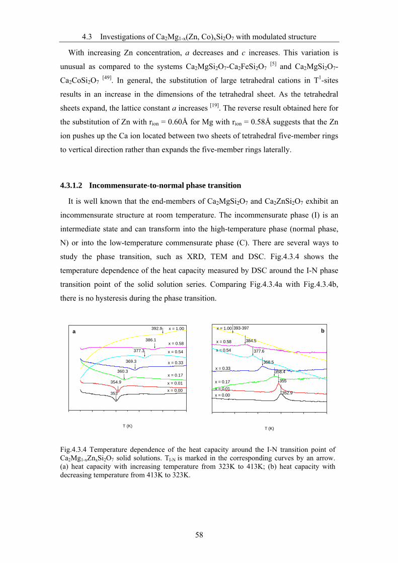
4.3 Investigations of Ca2Mg1-x(Zn, Co)xSi2O7 with modulated structure
With increasing Zn concentration, a decreases and c increases. This variation is
unusual as compared to the systems Ca2MgSi2O7-Ca2FeSi2O7 [5] and Ca2MgSi2O7-
Ca2CoSi2O7 [49]. In general, the substitution of large tetrahedral cations in T1-sites
results in an increase in the dimensions of the tetrahedral sheet. As the tetrahedral
sheets expand, the lattice constant a increases [19]. The reverse result obtained here for
the substitution of Zn with rion = 0.60Å for Mg with rion = 0.58Å suggests that the Zn
ion pushes up the Ca ion located between two sheets of tetrahedral five-member rings
to vertical direction rather than expands the five-member rings laterally.
4.3.1.2 Incommensurate-to-normal phase transition
It is well known that the end-members of Ca2MgSi2O7 and Ca2ZnSi2O7 exhibit an
incommensurate structure at room temperature. The incommensurate phase (I) is an
intermediate state and can transform into the high-temperature phase (normal phase,
N) or into the low-temperature commensurate phase (C). There are several ways to
study the phase transition, such as XRD, TEM and DSC. Fig.4.3.4 shows the
temperature dependence of the heat capacity measured by DSC around the I-N phase
transition point of the solid solution series. Comparing Fig.4.3.4a with Fig.4.3.4b,
there is no hysteresis during the phase transition.
a x = 1.00
x = 0.58
x = 0.54
x = 0.33
x = 0.17
x = 0.00
x = 0.01
353
354.9
360.3
369.3
377.3
386.1
392.9
T (K)
bx = 1.00
x = 0.58
x = 0.54
x = 0.33
x = 0.17x = 0.01x = 0.00
384.5
377.6
368.5
358.4
355
393-397
352.9
T (K)
Fig.4.3.4 Temperature dependence of the heat capacity around the I-N transition point of Ca2Mg1-xZnxSi2O7 solid solutions. TI-N is marked in the corresponding curves by an arrow. (a) heat capacity with increasing temperature from 323K to 413K; (b) heat capacity with decreasing temperature from 413K to 323K.
58
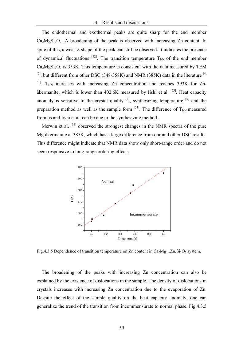
4 Results and discussions
The endothermal and exothermal peaks are quite sharp for the end member
Ca2MgSi2O7. A broadening of the peak is observed with increasing Zn content. In
spite of this, a weak λ shape of the peak can still be observed. It indicates the presence
of dynamical fluctuations [52]. The transition temperature TI-N of the end member
Ca2MgSi2O7 is 353K. This temperature is consistent with the data measured by TEM [5], but different from other DSC (348-358K) and NMR (385K) data in the literature [4,
31]. TI-N increases with increasing Zn concentration and reaches 393K for Zn-
åkermanite, which is lower than 402.6K measured by Iishi et al. [53]. Heat capacity
anomaly is sensitive to the crystal quality [4], synthesizing temperature [5] and the
preparation method as well as the sample form [53]. The difference of TI-N measured
from us and Iishi et al. can be due to the synthesizing method.
Merwin et al. [31] observed the strongest changes in the NMR spectra of the pure
Mg-åkermanite at 385K, which has a large difference from our and other DSC results.
This difference might indicate that NMR data show only short-range order and do not
seem responsive to long-range ordering effects.
0.0 0.2 0.4 0.6 0.8 1.0
350
360
370
380
390
400
Incommensurate
Normal
T (K
)
Zn content (x)
Fig.4.3.5 Dependence of transition temperature on Zn content in Ca2Mg1-xZnxSi2O7 system.
The broadening of the peaks with increasing Zn concentration can also be
explained by the existence of dislocations in the sample. The density of dislocations in
crystals increases with increasing Zn concentration due to the evaporation of Zn.
Despite the effect of the sample quality on the heat capacity anomaly, one can
generalize the trend of the transition from incommensurate to normal phase. Fig.4.3.5
59

4.3 Investigations of Ca2Mg1-x(Zn, Co)xSi2O7 with modulated structure
exhibits the phase diagram of Ca2Mg1-xZnxSi2O7 solid solution, which indicates an
almost linear increase of TI-N with the Zn/(Mg + Zn) ratio.
4.3.2 The Ca2Mg1-xCoxSi2O7 system
4.3.2.1 Average structure
As revealed by X-ray diffraction, the average structure of the melilite group shows
tetrahedral symmetry with the space group mP 124 . The projection of this basic
structure along the [001] direction is shown in Fig.4.3.6. A dashed square represents
the unit cell while a dotted square represents the subunit including one (Mg,Co)O4
tetrahedron and one Si2O7 dimer. Fig.4.3.7 shows an electron diffraction pattern of the
average structure of Ca2Mg0.75Co0.25Si2O7 crystal taken along the [001]. Only the
Bragg reflections of the unmodulated basic structure are observed.
Fig.4.3.6 Projection of the melilite structure along the c-direction.
Fig.4.3.7 Electron diffraction pattern of the average structure of Ca2Mg0.75Co0.25Si2O7.
The corresponding high-resolution image in Fig.4.3.8 exhibits the tetrahedral
average structure. By choosing some strong diffraction dots from the Fourier
transformation, a more clear structural image (Fig.4.3.8b) was obtained after Fourier-
filtering, which is completely consistent with the simulation image (inserted).
60

4 Results and discussions
Fig.4.3.8 (a) High-resolution image and corresponding Fourier transformation showing the average structure of Ca2Mg0.75Co0.25Si2O7; (b) inverse filtered Fourier transformation of (a) with the inserted multi-slice image simulation of the structure along with a model of the atomic positions within the unit cell.
4.3.2.2 Modulated structure
For the whole Ca2MgSi2O7-Ca2CoSi2O7 åkermanite series, the incommensurate
structure was detected by EDPs and HRTEM images in thicker sample regions.
Fig.4.3.9 shows the complex [001] zone diffraction pattern of Ca2Mg0.9Co0.1Si2O7 as
well as a schematic representation of the same diffraction pattern.
The most intense spots form a square grid corresponding to the basic reflections
due to the average structure. The first-, second- and even third-order of the
modulation can be observed as marked by the numbers 1, 2 and 3, respectively, in
Fig.4.3.9b. Normally, the intensity of these satellite spots weakens from the first to the
second and to the third order as observed from the experimental EDP. Relatively
intense satellites, which are due to combinations of the two modulation vectors, e.g.
q1 + q2 and q1 - q2, are also formed symmetrically on both [100] and [010] directions
between two basic reflections, which confirm that the modulation is two-dimensional
rather than the superposition of two one-dimensional modulations.
61

4.3 Investigations of Ca2Mg1-x(Zn, Co)xSi2O7 with modulated structure
Fig.4.3.9 (a) Electron diffraction pattern of Ca2Mg0.9Co0.1Si2O7 along [001] direction; (b) a schematic drawing of one enlarged reciprocal unit cell. The first-, second- and third-order satellites are indicated by numbers.
Fig.4.3.10 (a) A medium resolution image of Ca2Mg0.9Co0.1Si2O7 taken along the [001] direction. The two-dimensional modulation is indicated by M1 and M2. A “tartan-like” pattern is formed by intertwining of the modulation waves, which can be observed clearly from the inverse filtered Fourier transformation (inserted); (b) a high-resolution image of Ca2Mg0.5Co0.5Si2O7 taken along [113] direction. One-dimensional modulation is revealed from the image.
The two-dimensional modulation along [110] and [ 1 10] is directly observed in
Fig.4.3.10a, which shows a “tartan-like” pattern. This is revealed more clearly in the
inverse filtered Fourier transformation (inserted in Fig.4.3.10a). Such “tartan-like”
62

4 Results and discussions
pattern indicates the existence of nanometer-sized domains as observed in
Ca2ZnGe2O7 [28]. The modulation wavelength measured directly from the image is
about 21.8 Å. This value corresponds very closely to four times the dimension of a
subunit (5.53 Å). Along the modulation direction atomic arrays are detected which
alternatively show variations in density and brightness of the dots as indicated by two
parallel lines. This should be due to the overlapping of octagonal cell arrangements as
drawn in Fig.4 of literature [30]. A similar feature is observed in Fig.4.3.10b, but only
one-dimensional along [110].
0 20 40 60 80 100
285
290
295
300
305
310
q va
lue
(x 1
0-3)
x mol % Ca2Mg1-xCoxSi2O7
Fig.4.3.11 The q-value as a function of Co-content in Ca2Mg1-xCoxSi2O7 crystals. The value of every dot was the average of seven measured data from the corresponding EDPs.
The incommensurate structural modulation of the Ca2Mg1-xCoxSi2O7 system was
observed in the whole range of x at room temperature. The modulation vector q
calculated from the corresponding EDPs is plotted in Fig.4.3.11. With increasing
amount of Co, the modulation vector increases from 0.280 for Ca2MgSi2O7 to 0.307
for Ca2CoSi2O7. This tendency is the same as that observed by Seifert et al. [5] in
synthetic Ca2MgSi2O7-Ca2FeSi2O7 system.
63

4.3 Investigations of Ca2Mg1-x(Zn, Co)xSi2O7 with modulated structure
Fig.4.3.12 A medium image of Ca2Mg0.9Co0.1Si2O7 crystal revealing different structural information (a). Two-dimensional modulation observed by enlarged image (b) and the corresponding FFT (e) in thick area of the sample. One-dimensional modulation revealed from (c, f) and the unmodulated structure (d, g).
A medium resolution image of Ca2Mg0.9Co0.1Si2O7 with the large area is shown in
Fig.4.3.12a. Thickness of the sample increases from the right to the left according to
the wedge shape, which can be distinguished by changeable contrast. Two-
dimensional modulation was observed from area 1 (Fig.4.3.12b, e). In area 2, one can
observe one-dimensional modulation or the modulation exhibiting stronger in one
direction than another direction (Fig.4.3.12c, f). The unmodulated structure is
revealed in the area 3 (Fig.4.3.12d, g).
64

4 Results and discussions
The atomic position of the heavy cation of the constituent atom can be
distinguished from these high-resolution images, but the position of oxygen can not be
discerned. The resolution limitation of TEM itself and the weak scattering of the light
oxygen atom to the electron beam are reasons for that. In the modulated structure, it is
more difficult to resolve the atomic position. Although images are always taken in the
thin area, many layers of tetrahedral sheets are still included and the overlapping of
atoms also lowers the resolution.
The observations in a thick area show the two-dimensional incommensurate
modulation of Ca2Mg1-xCoxSi2O7 system at room temperature. Dark lines with
spacing of 3 and 4 subunits are observed along the two modulation directions and
alternating microdomains separated by such lines exhibit slightly different brightness
as investigated by von Heurck et al. [28]. They also observed various arrangements of
octagons from high-resolution images using a smaller objective aperture. At room
temperature, such arrangements of octagons partly overlap in a non-periodic way, but
almost completely overlap in the low-temperature lock-in structure as confirmed by
Schaper et al. [30].
4.3.3 Conclusions
The series of Ca2Mg1-xZnxSi2O7 crystals were grown by floating zone melting
method. The evaporation of Zn and the quality of a seed crystal influence the final
crystal quality. TI-N increases with the increase of the ratio of Zn/(Mg + Zn) from
353K for Ca2MgSi2O7 to 393K for Ca2ZnSi2O7.
The average structure of melilites was exhibited by the high-resolution image and
electron diffraction patterns in thin area in Ca2Mg1-xCoxSi2O7 system and all heavy
cation can be distinguished. Two-dimensional incommensurate modulation was
observed in thick area of the sample. The existence of microdomain structure was
revealed from high-resolution images.
65
4.4 Modulation and phase transitions of Ca2Co1-xZnxSi2O7
4.4 Modulation and phase transitions of Ca2Co1-xZnxSi2O7 in
dependence on temperature and composition
In this section, first the crystal characterization is described. The average structure
was resolved by high-resolution imaging and simulation. The two-dimensionally
modulated structure, including the variation of the modulation with the atomic
substitution as well as of the microdomain morphology, was studied by TEM. The
phase transition behavior was revealed by electron diffraction and thermal analysis.
The domains and discommensurations (DCs) formed during the phase transition are
described in detail. Finally, the crystal structure of the commensurate phase of
Ca2Co0.9Zn0.1Si2O7 was refined by XRD according to the orthorhombic space group
P21212 and the commensurate modulation was discussed.
4.4.1 Crystal growth and characterization
Crystals of the series of Ca2Co1-xZnxSi2O7 with x = 0.0, 0.1, 0.3, 0.5, 0.7, 0.9, 1.0
were grown by the FZ melting method. The charge rod and the seed crystal were
centered and mounted on the upper and lower shafts, respectively. The charge rod was
counter-rotated relatively to the rotation of the seed crystal with a speed of 40 rpm.
The growth rates were chosen between 0.5-1.2 mm/h.
The charge rods showed a color from pale blue to deep blue and, therefore, absorb
effectively the radiation energy, which is indicated by the close value between the
melting voltage and the stable voltage during growth. Supplementary 1 mol % ZnO
was added to all nominal charges except the end-member Ca2CoSi2O7 for
compensating the loss of ZnO during the growth process.
As already mentioned, low speeds have the advantage of avoiding possible crack
formations, the occurrence of bubbles, or inclusions. However, a too low growing
speed (< 0.5 mm/h) increases the unbalance of the components in the zone melting
process due to the evaporation of ZnO. On the other hand, high growing speeds (> 1.2
mm/h) may cause the formation of bubbles in the bulk. Therefore, in most
experiments, a speed of 1.0 mm/h was used. Note that under the condition of low
oxygen pressure, bubble-free crystals could be obtained at a growing speed higher
than the one in air atmosphere.
66

4 Results and discussions
Fig.4.4.1 shows macroscopic pictures of two as-grown crystals of the Ca2Co1-
xZnxSi2O7 system. The formation of microcracks approaching the crystal surface was
observed when the ratio of Zn/Co+Zn reached 0.5. These cracks increased in number
with increasing Zn content or prolonging the time of growth. Nevertheless, good
crystals could be obtained even at Zn contents as high as 70%.
Fig.4.4.1 Single crystals of Ca2Co0.7Zn0.3Si2O7 (a) and Ca2Co0.3Zn0.7Si2O7 (b) grown at ca. 1320 °C. The region of deep blue color corresponds to a length of 10mm; on the left hand side the seed crystal is seen.
Fig.4.4.2 XRD diagram of a Ca2ZnSi2O7 crystal: a) data of the ICSD standard; b) first as-grown crystal with large melting zone; c) second crystal grown applying a small melting zone. The arrows indicate peaks originating from the Ca3Si3O9 phase.
The growth of high purity crystal phases by the FZ technique generally requires a
careful control of the growth conditions and, in some cases, several repeats of the
growing run. For instance, in the end-member Ca2ZnSi2O7 a certain amount of
67

4.4 Modulation and phase transitions of Ca2Co1-xZnxSi2O7
Ca3Si3O9 has been found after the first experimental run: 5% according to the results
of XRD refinement (Fig.4.4.2a, b). Efforts to lower the evaporation of ZnO in a
second run have been successful through adjusting the zone volume to a size as small
as possible (Fig.4.4.2c).
All grown crystals were characterized by X-ray diffraction. The calculated and
observed relative intensities of the Ca2Co1-xZnxSi2O7 samples are in a good agreement,
which indicates a pure phase. The results for the example of Ca2Co0.5Zn0.5Si2O7 are
listed in Table 4.4.1 and plotted in Fig.4.4.3.
Table 4.4.1 Indices, 2 theta values, d-spacing and calculated and observed relative intensities of XRD analysis of Ca2Co0.5Zn0.5Si2O7
h k l 2Theta d-spacing Icalc. Iobs.0 0 1 17.653 5.02019 76 75 0 1 1 21.004 4.22617 26 26 1 1 1 23.908 3.71904 94 94 0 2 1 28.897 3.08723 138 155 1 2 1 31.115 2.87205 232 241 2 2 0 32.312 2.76835 18 17 0 0 2 35.743 2.51009 33 33 1 3 0 36.251 2.47609 58 58 2 2 1 37.054 2.42419 23 23 0 1 2 37.600 2.39028 30 37 0 3 1 38.858 2.31575 16 20 1 1 2 39.382 2.28613 19 21 1 3 1 40.593 2.22066 15 15 1 2 2 44.368 2.04010 48 47 1 4 0 47.860 1.89907 13 12 2 2 2 48.944 1.85952 30 29 1 4 1 51.402 1.77623 17 19 1 3 2 51.823 1.76276 101 106 2 4 0 52.202 1.75086 24 21 3 3 1 52.807 1.73222 16 14 1 1 3 57.487 1.60183 20 24 0 2 3 60.080 1.53873 20 21 1 2 3 61.352 1.50985 26 27 1 5 1 63.279 1.46844 15 16 2 4 2 64.879 1.43602 10 10 2 2 3 65.080 1.43209 21 22 0 3 3 66.297 1.40872 11 12 2 5 1 66.947 1.39661 15 15 1 3 3 67.502 1.38646 11 12 1 4 3 75.691 1.25551 15 17 0 0 4 75.724 1.25505 15 16 3 3 3 76.833 1.23968 12 14
68

4 Results and discussions
Fig.4.4.3 XRD diagram of Ca2Co0.5Zn0.5Si2O7 indicating the observed (blue line) and the calculated (red line) results. The difference between both is shown in the lower part.
Fig.4.4.4 XRD lattice parameters a and c versus composition in the system Ca2Co1-
xZnxSi2O7.
The refined lattice constants of Ca2Co1-xZnxSi2O7 obtained from the Rietveld
analysis are plotted in Fig.4.4.4. Because of the general rule that the substitution of
the T1-sites by larger tetrahedral cations should result in an increase in the dimensions
of the tetrahedral sheet, an increase of the a lattice parameter should be expected [53].
In the present system, the ionic radius of Zn2+ (0.60Å) is larger than that of Co2+
69
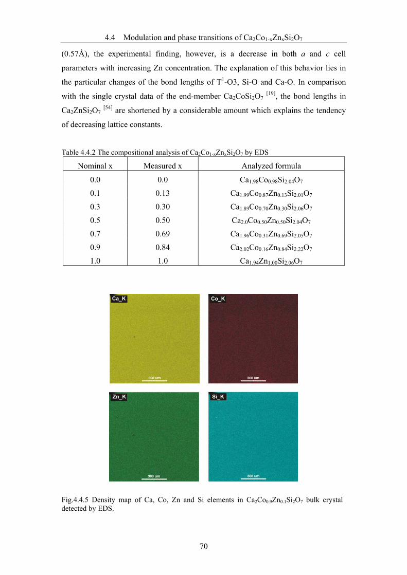
4.4 Modulation and phase transitions of Ca2Co1-xZnxSi2O7
(0.57Å), the experimental finding, however, is a decrease in both a and c cell
parameters with increasing Zn concentration. The explanation of this behavior lies in
the particular changes of the bond lengths of T1-O3, Si-O and Ca-O. In comparison
with the single crystal data of the end-member Ca2CoSi2O7 [19], the bond lengths in
Ca2ZnSi2O7 [54] are shortened by a considerable amount which explains the tendency
of decreasing lattice constants.
Table 4.4.2 The compositional analysis of Ca2Co1-xZnxSi2O7 by EDS
Nominal x Measured x Analyzed formula
0.0 0.0 Ca1.98Co0.98Si2.04O7
0.1 0.13 Ca1.99Co0.87Zn0.13Si2.01O7
0.3 0.30 Ca1.89Co0.70Zn0.30Si2.06O7
0.5 0.50 Ca2.0Co0.50Zn0.50Si2.04O7
0.7 0.69 Ca1.96Co0.31Zn0.69Si2.05O7
0.9 0.84 Ca2.02Co0.16Zn0.84Si2.22O7
1.0 1.0 Ca1.94Zn1.00Si2.06O7
Fig.4.4.5 Density map of Ca, Co, Zn and Si elements in Ca2Co0.9Zn0.1Si2O7 bulk crystal detected by EDS.
70
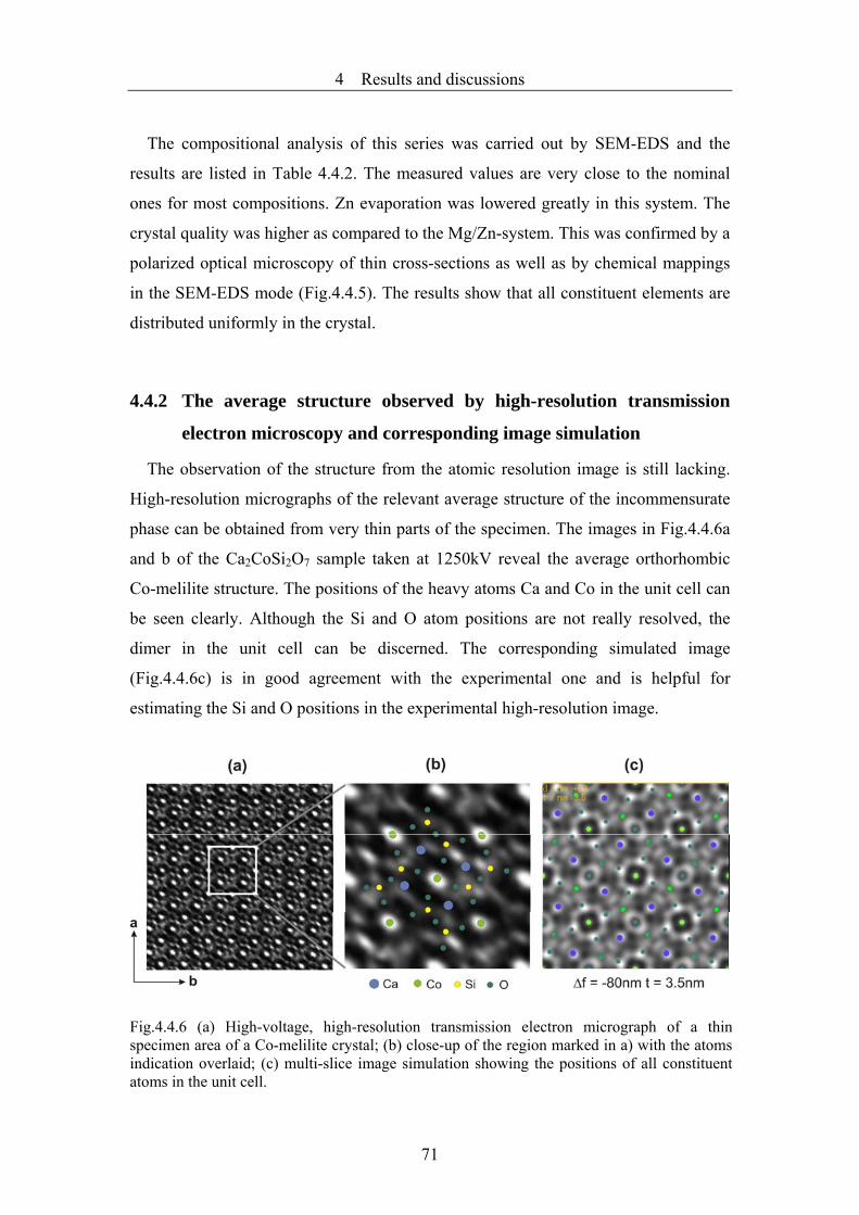
4 Results and discussions
The compositional analysis of this series was carried out by SEM-EDS and the
results are listed in Table 4.4.2. The measured values are very close to the nominal
ones for most compositions. Zn evaporation was lowered greatly in this system. The
crystal quality was higher as compared to the Mg/Zn-system. This was confirmed by a
polarized optical microscopy of thin cross-sections as well as by chemical mappings
in the SEM-EDS mode (Fig.4.4.5). The results show that all constituent elements are
distributed uniformly in the crystal.
4.4.2 The average structure observed by high-resolution transmission
electron microscopy and corresponding image simulation
The observation of the structure from the atomic resolution image is still lacking.
High-resolution micrographs of the relevant average structure of the incommensurate
phase can be obtained from very thin parts of the specimen. The images in Fig.4.4.6a
and b of the Ca2CoSi2O7 sample taken at 1250kV reveal the average orthorhombic
Co-melilite structure. The positions of the heavy atoms Ca and Co in the unit cell can
be seen clearly. Although the Si and O atom positions are not really resolved, the
dimer in the unit cell can be discerned. The corresponding simulated image
(Fig.4.4.6c) is in good agreement with the experimental one and is helpful for
estimating the Si and O positions in the experimental high-resolution image.
Fig.4.4.6 (a) High-voltage, high-resolution transmission electron micrograph of a thin specimen area of a Co-melilite crystal; (b) close-up of the region marked in a) with the atoms indication overlaid; (c) multi-slice image simulation showing the positions of all constituent atoms in the unit cell.
71

4.4 Modulation and phase transitions of Ca2Co1-xZnxSi2O7
Fig.4.4.7 (a-c) High-resolution images of different areas of thin specimens of Ca2CoSi2O7 taken by ARM-1250 microscope showing the average structure of the incommensurate phase; (d-f) The corresponding Fourier-filtered images by selecting most intense diffraction spots; (g-i) multislice image simulation for different defocus and thickness conditions using the EMS software package.
Fig.4.4.7a-c shows how the contrast of the lattice atoms varies with different
defocus and specimen thickness conditions. The inverse fast Fourier transforms (IFFT)
of the images by selecting the most intense diffraction spots provide better image
contrasts and a clearer structure imaging (Fig.4.4.7d-f). Corresponding multislice
image simulations are shown in Fig.4.4.7g-i for a variety of defocus and thickness
conditions. High-resolution images have also been taken using JEM 3010 microscope.
72

4 Results and discussions
Fig.4.4.8a-c shows three images taken at different defocus and thickness conditions
by JEM 3010 microscope. The corresponding IFFT and image simulations are given
for comparison (Fig.4.4.8d-i). Analyzing many high-resolution images, the
experimental images always showed a certain degree of distortion relative to the
corresponding simulations. Ruling out the error from operation and machine
conditions, this kind of distortion may come from the existence of the modulation,
which produces atomic shifts and deformation of the coordination polyhedra.
Fig.4.4.8 (a-c) High-resolution images of different areas of thin specimens of Ca2Co0.9Zn0.1Si2O7 taken by JEM 3010 microscope showing the average structure of the incommensurate phase; (d-f) The corresponding Fourier-filtered images by selecting most intense diffraction spots; (g-i) multislice image simulation for different defocus and thickness conditions using the EMS software package.
73

4.4 Modulation and phase transitions of Ca2Co1-xZnxSi2O7
4.4.3 Electron microscope studies of the modulated structure
In the Ca2Co1-xZnxSi2O7 system, satellite reflections of the modulated lattice were
observed in the (hk0) plane within the whole compositional range. Upon close
inspection of the diffraction patterns, systematic differences are observed between low
t and second
order satellites are clearly observed, and even
and high Zn content samples (Fig.4.4.9). While in the former the firs
third order reflections are weakly to be
detected, with increasing Zn content satellites higher than the first order disappear.
This behavior is illustrated by the two selected diffraction patterns inserted in
Fig.4.4.9 for the cases x = 0.1 (left inset), and x = 0.7 (right inset). As the diagram
curve shows, the changes in the intensity of the satellites goes along with an initial
increase and, above x ~ 0.5, nearly constant modulation wavelength in the <110>
direction at room temperature. Thereby, the wavelength ranges from 18.27 Å to
19.21Å.
gions, well distinguished with
respect to the appearance or disappearance of higher order satellites, to a high order
Fig.4.4.9 Variation of the modulation wavelength with increasing Zn content in Ca2Co1-
xZnxSi2O7, and typical [001] ED patterns for the case x = 0.1 (left inset) and x = 0.7 (right inset). Regions of high order (up to third order satellites are detectable), and of low order (only first order satellites are present) can be distinguished.
In a earlier publication Schosnig et al. reported a very similar behavior of the
satellite intensity of Sr-åkermanite in dependence on temperature during in situ
heating and cooling experiments. They denoted two re
[11]
74
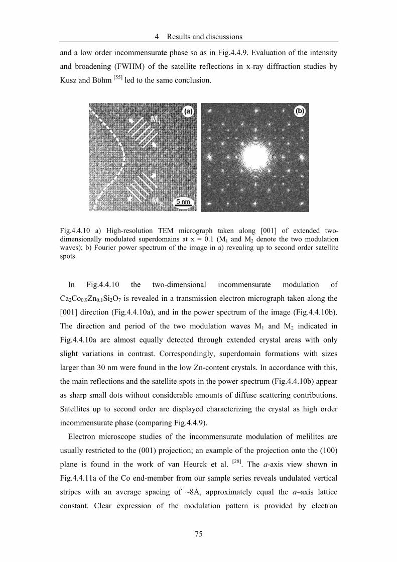
4 Results and discussions
and a low order incommensurate phase so as in Fig.4.4.9. Evaluation of the intensity
and broadening (FWHM) of the satellite reflections in x-ray diffraction studies by
Kusz and Böhm [55] led to the same conclusion.
irection and period of the two modulation waves M1 and M2 indicated in
Fig.4.4.10a are almost equally detected through extended crystal areas with only
sli
proximately equal the a–axis lattice
constant. Clear expression of the modulation pattern is provided by electron
Fig.4.4.10 a) High-resolution TEM micrograph taken along [001] of extended two-dimensionally modulated superdomains at x = 0.1 (M1 and M2 denote the two modulation waves); b) Fourier power spectrum of the image in a) revealing up to second order satellite spots.
In Fig.4.4.10 the two-dimensional incommensurate modulation of
Ca2Co0.9Zn0.1Si2O7 is revealed in a transmission electron micrograph taken along the
[001] direction (Fig.4.4.10a), and in the power spectrum of the image (Fig.4.4.10b).
The d
ght variations in contrast. Correspondingly, superdomain formations with sizes
larger than 30 nm were found in the low Zn-content crystals. In accordance with this,
the main reflections and the satellite spots in the power spectrum (Fig.4.4.10b) appear
as sharp small dots without considerable amounts of diffuse scattering contributions.
Satellites up to second order are displayed characterizing the crystal as high order
incommensurate phase (comparing Fig.4.4.9).
Electron microscope studies of the incommensurate modulation of melilites are
usually restricted to the (001) projection; an example of the projection onto the (100)
plane is found in the work of van Heurck et al. [28]. The a-axis view shown in
Fig.4.4.11a of the Co end-member from our sample series reveals undulated vertical
stripes with an average spacing of ~8Å, ap
75

4.4 Modulation and phase transitions of Ca2Co1-xZnxSi2O7
diffraction: The visible satellite reflections in Fig.4.4.11b (the reciprocal unit cell
viewed along [100] is marked by a black line) are due to combinations of the two
modulation vectors q1 and q2 with m × n = ± 1 and are, therefore, very closely spaced
on a*. They give rise to an averaged image contrast that overlies the regular (100)
lattice image. This superposition is supposed to be the reason for the formation of the
wavy stripes in the lattice image in Fig.4.4.11a.
The structural picture changes when the Zn-content in Ca2Co1-xZnxSi2O7 is
t order satellites. Its successful
etection strongly depends on the appropriate specimen thickness. The circular diffuse
in
Fig.4.4.11 a) TEM micrograph and b) selected area electron diffraction pattern along the [100] zone axis of Ca2CoSi2O7. The wavy stripes parallel c in the image are due to overlapping of the lattice planes and the modulation pattern formed by the combination ± (q1q2) of the two modulation vectors. The reciprocal unit cell is drawn in b).
increased up to x = 0.5 and higher. In the high-resolution image in Fig.4.4.12a,
variations in the modulated structure pattern are discernible which are reflected in the
Fourier power spectrum of the image in Fig.4.4.12b showing substantial diffuse
scattering intensity located on arcs connecting the firs
d
tensity patterns formed around the main reflections of the tetragonal lattice at radius
|q| are evidence of a short-range ordering scheme of the two-dimensional modulation
pattern.
76

4 Results and discussions
ig.4.4.12c. The modulation pattern varies from area to area in its propagation
di
Fig.4.4.12 a) TEM image of Ca2Co0.5Zn0.5Si2O7 taken along the [001] direction; b) corresponding Fourier power spectrum; c) filtered inverse Fourier transform clearly revealing the varying modulation pattern and arrangement of superdomains (domain boundary traces indicated); d) high-resolution close-up of the area marked in a) and c) with a few modulation periods and an octagonal cluster therein indicated.
The ordering is established in form of a complex arrangement of small
superdomains which can be seen only weakly in Fig.4.4.12a, but become developed
by appropriate filtering and processing of the Fourier transform as shown in
F
rection, phase of modulation wave and spatial coherency extent, thereby creating
irregular domains of sizes typically < 30 nm, on average. From a number of
observations it is suggested that the intensity of the diffuse scattering has its
maximum around x = 0.5 and decreases towards larger values of x. This behavior is
indicative of a contribution by occupational ordering of Co and Zn species to the
overall displacive modulation and ordering.
77

4.4 Modulation and phase transitions of Ca2Co1-xZnxSi2O7
Diffuse scattering due to short-range ordering within a many-domain structure that
has been observed here in dependence on compositional variations, also occurs when
the temperature changes. It is typically an intermediate state in phase transitional
processes as will be show in a forthcoming subpart.
n Heurck et al. [28], Riester et al. [16
he normal phase
The incommensurate - commensurate phase transition
incomm ealed from the
ositional shift of the satellite reflections. Fig.4.4.13 shows the electron diffraction
different temperatures for
1h
lites tended to shift closely each other along [110] or [1
Fig.4.4.12d is a close-up of the area framed in Fig.4.4.12a showing the modulation
pattern at atomic resolution. Several modulation periods are indicated along with the
octagonal arrangement of bright intensity dots that mark a typical cluster formation of
T1 tetrahedra. Such a clustering was predicted by va], Kusaka et al. [19], and Hagyia et al. [56]. According to these models the misfit-
induced strains cause changes of the Ca-O bonding resulting in a reduction of the
calcium-to-oxygen coordination from eight- to six-fold for different sections through
the superspace. Internal stress release is the driving force for the modulation
formation. It is realized on both a nanoscopic as well as microscopic scale by
octagonal clustering of the low-coordinated calcium polyhedra as well as by the
introduction of a network of domain boundaries.
4.4.4 The transition from the incommensurate phase to the
commensurate lock-in phase and to t
With changing temperature, the process of the phase transition from the
ensurate to the commensurate lock-in state could be rev
p
patterns of Ca2Co0.9Zn0.1Si2O7 taken after cooling down to
.
At 297K an incommensurate structure exists (Fig.4.4.13a). The satellite reflections
up to second order can be observed clearly as marked by numbers. Upon cooling
down to 168K, evident diffuse scattering of satellites was observed (Fig.4.4.13b).
Satel 1 0] as indicated by
arrows. Finally, the commensurate lock-in structure was formed as shown in the EDP
taken at 91K (Fig.4.4.13c).
78

4 Results and discussions
0.335
50 100 150 200 250 3000.295
0.300
0.305
0.310
0.315
0.320
0.325
0.330
q ve
ctor
T (K)
decrease temp. increase temp.
der to reach thermal equilibration of the
tructure, every EDP was taken after the temperature remained unchanged for 1h.
W
Fig.4.4.13 Electron diffraction patterns of Ca2Co0.9Zn0.1Si2O7 depending on temperature. a) Incommensurately modulated structure at 297K; b) diffuse scattering around Bragg reflections indicating the occurrence of the phase transition from the incommensurate to the commensurate lock-in phase at 168K; c) the commensurate lock-in structure at 91K.
Fig.4.4.14 The q-value as a function of temperature for the Ca2Co0.9Zn0.1Si2O7 crystal calculated from the corresponding EDPs. The sharp increase of the q-value between 175K and 130K indicated the phase transition occurred.
The change of the modulation vector with temperature calculated from EDPs is
shown in the diagram Fig.4.4.14. In or
s
ith the lowering of temperature from 300K to 91K, the q-vector is related linearly to
temperature within the intermediate incommensurate phase, and then jumps to 0.331
at about 130K. After that, it remains constant. The jumping of the modulation wave
vector between 175K and 130K indicates the phase transition from the
79

4.4 Modulation and phase transitions of Ca2Co1-xZnxSi2O7
incommensurate to the commensurate lock-in phase. The q value with varying
temperature from 90K to 300K is also given in Fig.4.4.14. It begins to decrease
rapidly after 200K. A strong hysteresis exists between the cooling and heating run of
the in situ experiments.
0.34
180 200 220 240 260 280 3000.29
0.30
0.31
0.32
0.33
q ve
ctor
T (K)
increase temp.
s also investigated by X-ray diffraction (Most XRD
easurements and all refinements mentioned later were carried out by Prof. Werner
M
Fig.4.4.15 The q-value as a function of temperature for the Ca2Co0.9Zn0.1Si2O7 crystal was investigated by single crystal X-ray diffraction. The measurements conformed to the ascending temperature sequence.
For comparison, the structural variation of the same crystal with temperature at
cooling from 300K to 90K wa
m
assa, Chemistry Department). The results in Fig.4.4.15 show the same tendency of
the q-value as observed from the EDPs. However, the transformation point from the
commensurate to the incommensurate phase measured by X-ray diffraction was about
250K which is higher than 200K measured by EDPs. This difference can be explained
by the differently measured range. The measured area in electron diffraction is in the
order of nanometer. As it is discussed in the following, domains in the order of
nanometer are formed during the phase transition and the point of the phase transition
is different from one domain to another. The q-value obtained from the electron
diffraction represents very local structural information of the crystal. On the contrary,
the measurement of X-ray diffraction is related to millimeter scale and, thus, gives
more average information. Another possible reason is due to the influence of the
80

4 Results and discussions
electron beam irradiation in the microscope. The formation of domains described later
are considered responsible for the phenomenon of the prominent hysteresis observed
by X-ray diffraction [29] and in our experiments.
The phase transition into the commensurate lock-in phase was found to occur up to
x-values < 0.5 at liquid nitrogen (LN2) temperature. Considering the plenty of EDPs
taken from different areas under the phase transition temperature, it was found that the
process of the phase transition is rather slow and also uneven from place to place.
Some areas started the phase transition firstly, but other areas not yet even at much
lower temperature. This is proved by Fig.4.4.16, where quite different diffraction
patterns from different areas of the same sample at 126K represent the
incommensurate phase (Fig.4.4.16a) and an almost commensurate lock-in phase
(Fig.4.4.16b). The quite different domain formations result in the hysteresis
phenomenon described above.
2CoSi2O7 with
rolonging cooling time and lowering temperature. Many domains separated by the
alls are formed at the beginning of the
ph
Fig.4.4.16 The EDPs of Ca2Co0.9Zn0.1Si2O7 crystal taken from different areas at 126K, indicating that incommensurate and commensurate domains exist in parallel.
Microdomains and discommensurations
Fig.4.4.17 shows a domain structure and its evolution in Ca
p
intersection of discommensuration (DC) w
ase transition (Fig.4.4.17a). The size of the majority of the domains was about
10nm. With further cooling and proceeding time the domains increased in size
81

4.4 Modulation and phase transitions of Ca2Co1-xZnxSi2O7
(Fig.4.4.17b-d) and finally developed into a random network structure (Fig.4.4.17e).
Lowering the temperature accelerated the increase of the domains in size.
Fig.4.4.17 Bright-field electron micrographs taken during the phase transition showing microdomains and the changes of the domains and the discommensuration network with time at decreasing temperature: (a) t1 = 50min at 150K; (b) t2 = t1 + 30min at 100K; (c) t3 = t2 + 30min; (d) t4 = t3 + 40min; (e) t2 = t4+ 50min.
82

4 Results and discussions
Fig.4.4.18 shows some domains of Ca2CoSi2O7 observed in the same specimen area
area almost reached the commensurate lock-
phase.
at 130K after different cooling times. As indicated in the images, the width of one
domain was about 70 nm and kept the same in size and shape during cooling for 240
min up to 360 min, which means that the
in
Comparable TEM measurements under liquid He condition are shown in Fig.4.4.19.
Even at He temperature, the uncompleted commensurate lock-in phase could still be
observed (Fig.4.4.19a) [57]. A high-resolution image taken at this temperature shows
two dimensional modulations assigned as M1 and M2 (Fig.4.4.19b).
Fig.4.4.18 Microdomain in Ca2CoSi2O7 taken at 130K in other area after cooling different time. a) 240 min; b) 300 min; c) 360 min.
Fig.4.4.19 Electron diffraction pattern (a) and high-resolution image (b) of Ca2CoSi2O7 taken at liquid He temperature. M1 and M2 assign to two-dimensional modulated directions.
83
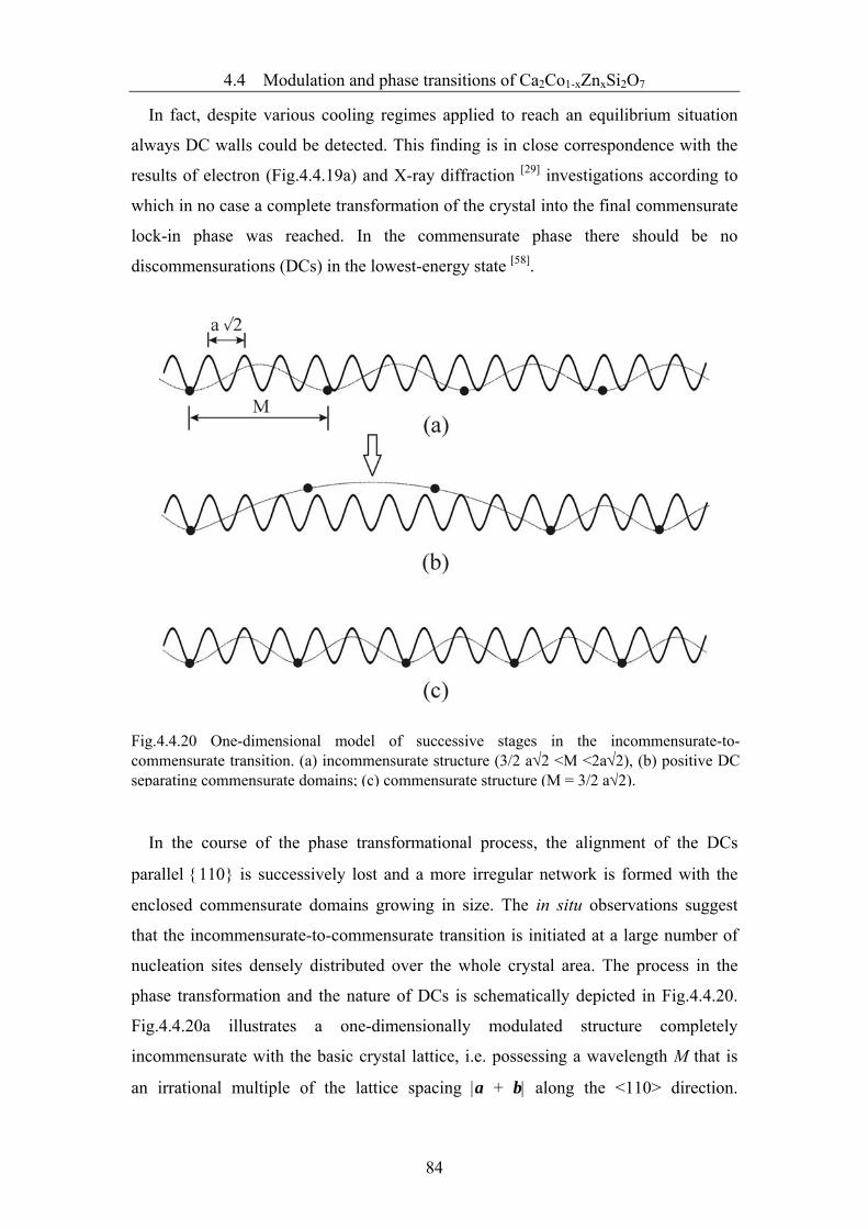
4.4 Modulation and phase transitions of Ca2Co1-xZnxSi2O7
In fact, despite various cooling regimes applied to reach an equilibrium situation
always DC walls could be detected. This finding is in close correspondence with the
results of electron (Fig.4.4.19a) and X-ray diffraction [29] investigations according to
which in no case a complete transformation of the crystal into the final commensurate
lock-in phase was reached. In the commensurate phase there should be no
discommensurations (DCs) in the lowest-energy state [58].
In the course of the phase transformational process, the alignment of the DCs
parallel 110 is successively lost and a more irregular network is formed with the
enclosed commensurate domains growing in size. The in situ observations suggest
that the incommensurate-to-commensurate transition is initiated at a large number of
nucleation sites densely distributed over the whole crystal area. The process in the
phase transformation and the nature of DCs is schematically depicted in Fig.4.4.20.
Fig.4.4.20a illustrates a one-dimensionally modulated structure completely
incommensurate with the basic crystal lattice, i.e. possessing a wavelength M that is
an irrational multiple of the lattice spacing |a + b| along the <110> direction.
Fig.4.4.20 One-dimensional model of successive stages in the incommensurate-to-commensurate transition. (a) incommensurate structure (3/2 a√2 <M <2a√2), (b) positive DC separating commensurate domains; (c) commensurate structure (M = 3/2 a√2).
84

4 Results and discussions
Approaching the phase transitional temperature region, the rearrangement and dense
packing on the nanometer level of the structural units under the influence of
increasing misfit stress leads to the nucleation of commensurate ‘islands’ within the
commensurate phase (Fig.4.4.20b). The commensurate kernels grow on the expense
of
in
the number (and of the width) of the incommensurate walls (Fig.4.4.20c), which
adopt the character of narrow boundaries: these boundaries we call
discommensurations. In this view, the DCs represent regions where the developing
commensurate registry between the basic lattice and the modulation wave is broken [59].
Fig.4.4.21 Discommensuration loop observed at 130K. (a) original image; (b) Fourier-filtered image using the eight basic orthorhombic reflections; (c) Fourier-filtered two-beam (± 100) lattice fringe image with dislocation-like defects arrowed.
Within the above-described two-dimensionally extended networks special
configurations of the DCs were observed, such as those in Fig.4.4.21. The relevant
information is selected by Fourier-filtering of the original high-resolution micrograph
(Fig.4.4.21a) using the eight basic nearest hk0 reflections of the orthorhombic
lattice (Fig.4.4.21b), or the two (± 100) spots only (Fig.4.4.20c). Fig.4.4.21c is
synonymous with a symmetrical two-beam lattice fringe image. What cannot be seen
in the original unprocessed image is revealed in Fig.4.4.21b: the central area of the
image contains an almost circularly shaped domain with very homogeneous structure,
enclosed by a DC boundary loop. Relics of a tetragonal mesh built-up by orthogonally
intersecting DCs surround the loop. Fig.4.4.21c clearly displays a lattice shift across
ith the presence of dislocation-
the DC constituting the loop as well as DCs separating other domains parts in the
surrounding crystal. This shift is usually connected w
85

4.4 Modulation and phase transitions of Ca2Co1-xZnxSi2O7
like defects as they are pointed out by arrows. Such a shift of the lattice fringes
alongside a discommensuration was detected also in other materials, e.g., by Jiang and
Zou [60]. However, the actual situation in the present case is more complicated than it
is shown in Fig.4.4.21c where only one crystal orientation has been filtered out for
clarity.
The formation of loops clearly indicates the tendency of the DCs to adopt low-
energy configurations. Quite a similar behavior is well known from dislocation type
defects [61, 62].
The incommensurate - normal phase transition
The phase transition of Ca2Co1-xZnxSi2O7 from the incommensurate to the normal
state was investigated by DSC between 350K and 500K and the results are shown in
Fig.4.4.22. The TI-N of Co and Zn end members are 478K and 390K, respectively,
similar to the results of Röthlishberger et al. [7]. TI-N shifts to lower temperature with
increasing Zn content and the peaks become broader. The heating and cooling
investigations revealed the peak of the heat capacity at the same temperature, which
indicates no hysteresis between the incommensurate and the normal phase transition.
340 360 380 400 420 440 460 480 50 520 540 5600
x = 1.0
x = 0.7
x = 0.5
x = 0.3
x = 0.0
T (K)
Fig.4.4.22 Temperature dependence of the heat capacity of Ca2Co1-xZnxSi2O7 compounds. The endothermal peak as indicated by arrow appears during the phase transition from the incommensurate to the normal structure.
86

4 Results and discussions
Table 4.4.3 TI-N and TI-C obtained through the measurements of the heat capacity of Ca2Co1-
xZnxSi2O7 solid solutions.
0
0
400
700
500
600
0.0 0.2 0.4 0.6 0.8 1.0
10
200
300
Commensurate
Ca2CoSi2O7Ca2Zn 2 7Zn
K)
The temperature of the phase transition of the Ca2Co1-xZnxSi2O7 system as
vestigated by DSC are listed in Table 4.4.3 and plotted in Fig.4.4.23. The data about
the I-C phase transition are included. The TI-N values exhibit a linear decrease with
increasing Zn content, similar to that in Ca2Mg1-xZnxSi2O7 solid solutions.
The hysteresis between the incommensurate and the commensurate phase transition
was revealed, but no hysteresis existed between the incommensurate and the normal
phase transitions.
Zn/(Co+Zn) TI-N (K) TI-C (K)
Normal
IncommensurateT (
-content Si O
0.0 478 153.7
0.1 477.7 146.5-165
0.3 463.6 145.5-123
0.5 446.4 -
0.7 422.7 -
0.9 404 -
1.0 388-394 -
Fig.4.4.23 Phase diagram of Ca2Co1-xZnxSi2O7 . system
in
87
4.4 Modulation and phase transitions of Ca2Co1-xZnxSi2O7
4.4.5 Refinement of the commensurate lock-in structure of
Ca2Co0.9Zn0.1Si2O7
As indicated by the q-vector measured by X-ray diffraction the almost
commensurate phase can be reached at liquid N2 temperature, and reversed into the
incommensurate phase at temperature higher than 250K. In the commensurate phase
the satellite reflections are located on rational positions with respect to the main
reflections in the reciprocal lattice. McConell [63] derived by group theoretical
methods 4P and as only suitable subgroups that are related to the modulation
of the me e. The space group
222 11P
lilite structur 4P was used for the description of the
commensurate lock-in phase of Ca2CoSi2O , but refinements as (110) twin could
etry for all SiO4 groups and by
sing common isotropic displacement parameters. Based on the diffraction studies of
Ca
7 [16]
be held stable only by applying constraints in geom
u
2CoSi2O7 at low temperature, Hagiya et al. [56] refined the same structure according
to 4P and 222 11P and found much better agreement of satellite intensities for the
latter space group.
Based on our area detector data measured at 190K for Ca2Co0.9Zn0.1Si2O7 we
performed refinements of both models and could clearly confirm the results of Hagiya.
Though all atoms could be refined without any positional constraints in s.g. 4P , some
of the displacement parameters became irregular. Even for the heavy Ca and Co
atoms, refinement of anisotropic parameters became unstable, the residuals were wR
sensible anis ent parameters could be refined. Even for most of the O
at
) and R = 6.05% (F>2σ). The crystal data, structure refinement parameters and
the interatomic distances are given in Appendix A. for s.g. and in Appendix B.
2
= 19.4% (all F2) and R = 7.56% (F>2σ). In s.g. 222 however, for all heavy atoms
otropic displacem
11P
oms good anisotropic displacement parameters could be refined, but for the final
cycles isotropic parameters were used only in order to reduce the number of
parameters. The crystal structure has been refined in the orthorhombic space group
222 11P as (110)-twin with a twin ratio of 46.5(3)%. The residuals were wR2 = 15.6% 2(all F
222 11P
for s.g. 4P .
The mean Si-O distance of each tetrahedron ranges from 1.620(10) to 1.643(9)Å.
The distance between the Si and O atoms bridging two Si tetrahedra forming a dimer
is the longest Si-O distance and the bond length between Si and the apical O atom is
88

4 Results and discussions
the shortest. Taking into account both bond length and bond angle five classes of Si
tetrahedra exist in the 3×3 super unit.
Co1
Si1
Co2
Co3
Si2
Si4
Co4O2
Si6
Si7O6
Si3
O21
O22
Si5
O19
O20Co5O3
Si8O7
O5
Si9
Ca1
O11
O23
O24
O12
O32
Ca3 O31
Ca4
O15
Ca2
Ca6
O13
Ca7
O1O16
O9
Ca9
Ca5
O8
O17
O26
O27
Ca8O10
O18
O4
O28
O25 O14
O29
O30
a
b
c
As known from the structural description of the average structure, Ca atoms are
located between the tetrahedral layers and are surrounded by eight O atoms. In the
3×3 superstructure, the Ca-O distances of each polyhedron show wide variations
(Fig.4.4.24). Based on a critical bond length of 2.6 Å, the Ca polyhedra can be
assigned to be of six-fold (Ca5, Ca6, Ca8, Ca9), of seven-fold (Ca2) and of eight-fold
coordination (Ca1, Ca3, Ca4). The “bundles” of the six-fold coordinated Ca polyhedra
were suggested to form octagonal arrangements [16, 18], which is thought to be
responsible for the formation of the incommensurate phase.
Fig.4.4.24 The commensurate lock-in structure of Ca2Co0.9Zn0.1Si2O7 determined at 190K. Projection of a part of the structure from about [001]. All atoms of the asymmetric unit are labeled (same selection and labeling scheme as in Hagiya et al. 2001).
89

4.4 Modulation and phase transitions of Ca2Co1-xZnxSi2O7
90
°. In comparison to the
corresponding values in Ca2CoSi2O7 [56], the substitution of Zn for Co makes the T1O4
tetrahedra to become more distorted. The rotation of T1O4 tetrahedra is evident and
varies from one to another (Fig.4.4.25). The rotation angle between the a axis and one
of the T1-O bonds of each tetrahedron projected on the (001) plane was determined
Fig.4.4.25 Projection of the T1 tetrahedra of the commensurate lock-in structure of Ca2Co0.9Zn0.1Si2O7 in [001]. T1 sites actually occupied by Co and Zn. The angle formed by the Co-O bond and a axis is named as Co1, Co1a, Co2 and so on.
There are five independent Co(Zn) atoms in the 3×3 superstructure. The mean
(Co,Zn)-O distances of T1O4 tetrahedra are in the range 1.945(9) – 1.958(9)Å, which
is the same as obtained by Hagiya et al. [56] in Ca2CoSi2O7. The substitution of a small
amount of Zn for Co in the T1O4 tetrahedra has no evident effect on the T1-O bond
because of the close ionic radius. Each tetrahedron shows a distortion and a rotation
with different degree. Especially, the Co,Zn(5) tetrahedron is very much flattened
along [001] and the two independent angles intersecting [001], 127.1° and 125.4°, are
much larger than the regular tetrahedral angle of 109.47

4 Results and discussions
and marked in Fig.4.4.25. The angle varies from 15.3° for the Co,Zn (3a) tetrahedron
to 40.1° for the Co,Zn (5) tetrahedron.
0 2 4 6 8 10 12 14 16 1814
16
18
20
22
24
26
28
Rot
atio
n an
gle
(?
Unit cell number
Ca polyhedra, which characterizes the incommensurate structure [18, 37], is not found in
the commensurate phase. The structural models in
The octagonal distribution of the bundles formed by T1-tetrahedra and four six-fold
4P and P show different 222 11
arrangement of “clusters” with 6-coordinated Ca. In the 4P model of Riester et al. [16]
octagons can be seen. But the clusters are more dilute and show no octagons in the
4P model of Hagiya and in the 4P model used in this work. In the 222 11P model,
there are no complete octagons only parts of it. Many fractions of the octagons are
scattered in the structure. The commensurate modulation must be due to other reason.
Considering the structural analysis from our experimental data the strong rotation of
these tetrahedra as well as the tetrahedra distortion should contribute to the strain of
tetrahedra sheet relative to the Ca polyhedra and regard as the main reason of the
formation of the incommensurately modulated structure. In the commensurate lock-in
phase a saw-tooth-like variation of Co,Zn-tetrahedra along a and b directions can be
observed clearly, formed due to the different rotation of Co,Zn-tetrahedra. Fig.4.4.26
shows a saw-tooth-like variation in one dimension. The saw-tooth-like variation
Fig.4.4.26 A saw-tooth-like ordering repeating according to the 3×3 superstructure Each solid spot represents a T1-tetrahedron.
91

4.4 Modulation and phase transitions of Ca2Co1-xZnxSi2O7
repeats according to the 3×3 super unit, which was not observed in the
incommensurate phase until now, is assumed as the equilibrium state of lowest energy.
his periodic ordering along a and b directions, formed by the distortion and rotation
of Co,Zn-tetrahedra, especially the rotation of Co,Zn-tetrahedra, causes the
commensurate modulated structure with q = 1/3.
4.4.6 Conclusions
Single crystals of Ca2Co1-xZnxSi2O7 free of inclusions and bubbles could be
obtained through precise control of the growing speed. Using a small melting length
made it possible to efficiently avoid undesired evaporation of Zn during the growth
process.
Two-dimensional incommensurate modulation of the Ca2Co1-xZnxSi2O7 structure
was observed by electron diffraction and high-resolution imaging. Different ordering
schemes within the modulated structure were observed, and changes of the domain
icator of short-range ordering associated with the
commensurate modulation. The octagonal arrangement of T1 tetrahedra surrounded
by
that the growing commensurate phase becomes separated by a network of straight
embles large-scale regular
pos
T
morphology were found in dependence on the Co/Zn ratio. The diffuse diffraction
intensity has been proved a clear ind
in
six-coordinated Ca atoms could be confirmed by HRTEM observations.
The phase transition process of Ca2Co0.9Zn0.1Si2O7 does not occur homogeneously
over extended crystal areas but is initiated at a great number of nucleation sites, and
DCs. In an early state of development the network res
“bundles composed of four CaO6 arrays and a central array of CaO4 tetrahedra” as
tulated in a recent simulation treatment by Kusaka et al. [64]. Progress in the very
slow first order I-C transition process can be thus read, on a mesoscale, from the
increasing separation of the DC lines. The equilibrium commensurate phase could be
approached but not reached completely as the number of DCs show which survived
even after prolonged and deep cooling. The TI-C and TI-N decreased slightly with
increasing amount of Zn.
The commensurate lock-in structure is orthorhombic P21212. The substitution of Zn
for Co makes the T1O4 tetrahedra even more distorted. The distortion and rotation of
92

4 Results and discussions
T1-tetrahedra is responsible for the commensurately modulated structure of
Ca2Co0.9Zn0.1Si2O7.
93

4.5 Investigations of the structural modulation of (Ca1-xSrx)2CoSi2O7
4.5 I ves igationn t s of the structural modulation of (Ca1-xSrx)2CoSi2O7
The temperature TI-N at which the incommensurately modulated structure turns into
the basic high-temperature structure depends on the chemical composition of the
melilites. Ca2CoSi2O7 with TI-N = 210-220°C shows the incommensurate structure at
room temperature, but Sr2CoSi2O7 with TI-N << 24°C shows the basic structure at
room temperature [7]. The shift of TI-N with the substitution of Sr for Ca is interesting
and helpful to understand the strain release by enlarging the cell. This chapter
describes the single crystal growth of (Ca1-xSrx)2CoSi2O7. The chemical analyses were
carried out by EDS and WDS. The structural variation caused by the substitution of Sr
for Ca in (Ca1-xSrx)2CoSi2O7 was investigated by TEM and XRD methods.
Measurements were carried out to determine the magnetic behavior of the material.
4.5.1 Crystal characterization
To obtain a crystal with a certain composition synthetic Ca- and Sr-end member
melilites were proportionally mixed and prepared into the nutrient rods for crystal
growth. The crystal growth of this system is comparatively easy because all raw
materials used are stable at high temperature. Comparing with the (Ca1-xSrx)2MgSi2O7
solid solutions, which were grown in the range x ≤ 0.32 using the Czochralski
technique [9], high-quality single crystals of (Ca1-xSrx)2CoSi2O7 in the whole range of
x were grown in air from the melt using the FZ method.
Diameter and length of the growing crystal can be adjusted by controlling the
moving speeds of the upper and lower shaft and the length of the nutrient rod. Single
crystals of ca. 3mm diameter and ca.20mm length were obtained shown in Fig.4.5.1.
The crystals are dark blue. The observation of a smooth surface and the
characterization by polarized optical microscopy confirmed that the crystals are of
good quality i.e. free of bubbles, cracks and inclusions. The numbered areas (see
figure caption) of the bulk crystal were used for different investigations.
The good agreement of the observed and calculated diffraction peaks confirms the
pure phase. From all crystals EDS chemical analyses were performed. The
measurements were carried out in different areas of each sample. The mean values are
listed in Table 4.5.1. They are rather close to the nominal ones.
94

4 Results and discussions
95
Table 4.5.1 The chemical analysis of (Ca1-xSrx)2CoSi2O7 by EDS Nominal x Measured x Analyzed formula
0.00 0.00 Ca1.98Co0.98Si2.04O70.10 0.10 (Ca0.90Sr0.10)2Co0.98Si2.06O70.12 0.11 (Ca0.89Sr0.11)2Co0.96Si2.13O70.25 0.25 (Ca Sr ) Co Si O0.75 0.25 2 0.98 2.08 70.30 0.30 (Ca0.70Sr0.30)2Co0.96Si2.09O70.35 0.36 (Ca0.64Sr0.36)2Co0.96Si2.27O70.50 0.57 (Ca0.43Sr0.57)2Co0.96Si2.23O70.75 0.71 (Ca0.29Sr0.71)2Co0.83Si2.04O7
The crystal (Ca0.75Sr0.25)2CoSi2O7 was also investigated by WDS technique for
comparison. The diameter of the beam selected was 10µm and 30 points along both x
and y were selected for analysis. The weight percent of each element as oxide shows
an almost straight line along the points (Fig.4.5.2), which means that the constituent
elements are homogeneously distributed in the bulk crystal. The content of Sr and Ca
is the same as the nominal concentration.
Fig.4.5.1 The as-grown crystal of (Ca0.75Sr0.25)2CoSi2O7. The length and the diameter of the crystal are 23mm and 3mm, respectively. The areas marked by numbers were used for a
rystal for other growth; (2) for single crystal X-ray analysis by EDS and WDS; (5) for magnetic
m
variety of measurements. (1) as seed cdiffraction; (3) for TEM; (4) for compositional
easurements; (6) for phase identification by X-ray powder diffraction.

4.5 Investigations of the structural modulation of (Ca1-xSrx)2CoSi2O7
10.00
15.00
20.00
25.00
30.00
35.00
40.00
1 3 5 7 9 11 13 15 17 19 21 23 25 27 29
points
oxid
e-w
t%SiO2
CaO
CoO
SrO
Cell parameters of (Ca0.75Sr0.25)2CoSi2O7 were determined using the intense
Fig.4.5.2 The correlation of the weight percent of each element as oxide with the measured spots by WDS.
reflections in the range of 3.65 ≤ θ ≤ 29.15 at 233K. The basic structure was refined
nt in the non-centrosymmetric space
group
only using the main reflections. The refineme
m124 by thP e least-square
main reflec led to R(F) = 0.0207 R(F) = 0.05 nt
and the refi
The basi cture of (Ca0.75Sr0.25 i2O7 determ in
Fig.4.5.3. The structural features are s to those o ]
and Ca2Co [12]. The structure is characterized by a strong anisotropy of the
isplacement ellipsoid of all O and Ca/Sr atoms which lie almost in the (001) plane
nd the long axes of the ellipsoids are oriented toward the <110> direction except the
ax
plitudes of the displacive modulation and
the occupational disorder due to the substitution of Ca by Sr.
s program SHELXL-97, using 438 independent
tions, and w 19. tai o the xp imeDe ls f e er
nement are summarized in Table 4.5.2.
c stru )2CoS ined 2 K is p d at 33 de icte
imilar f (Ca0.87Sr0.13)2CoSi2O7 [12, 15
Si2O7
d
a
is of O(3). The ellipsoids of Co and Si are almost spherical. O(1) bridging the two
tetrahedra in the Si2O7 dimer shows the largest anisotropy. The shift of O(1) towards
the center of the channels should be coupled with the displacement of the Ca/Sr atoms
located in the channels, because the displacement directions of Ca/Sr and O(1) atoms
are mutually perpendicular. The anomalously large displacement feature in the
average structure probably reflects the am
96

4 Results and discussions
Table 4.5.2. Crystal data and main structure refinement for (Ca0.75 Sr0.25)2Co Si2 O7 at 233 K Empirical formula Ca1.57 Sr0.43 Co Si2 O7Formula weight 327.71 Temperature 233(2) K Wavelength 0.71073 Å Crystal system tetragonal
Space group P 1m Unit cell dimensions a = 7.8912(9) Å α = 90°. b = 7.8912(9) Å β = 90°. c = 5.0461(6) Å γ = 90°. Volume 314.23(6) Å3 Z 2 Density (calculated) 3.464 Mg/m3 Absorption coefficient 7.993 mm-1 F(000) 317 Crystal size 0.36 x 0.22 x 0.16 mm3
-10<=h<=10, -10<=k<=10, -6<=l<=6 Reflections collected 2661
dependent reflections 438 [R(int) = 0.0270] Co Ab
indices
d -0.443 e.Å-3
_4 2
Theta range for data collection 3.65 to 29.15°. Index ranges
Inmpleteness to theta = 29.15° 94.0 % sorption correction multi-scan
Refinement method Full-matrix least-squares on F2 Data / restraints / parameters 438 / 0 / 35 Goodness-of-fit on F2 1.197 Final R [I>2sigma(I)] R1 = 0.0208, wR2 = 0.0520 R indices (all data) R1 = 0.0210, wR2 = 0.0521 Absolute structure parameter -0.02(3) Extinction coefficient 0.028(12) Largest diff. peak and hole 0.592 an
Interatomic distances (Table 4.5.3) show that (Ca,Sr) is coordinated by t
oxygens and the (Ca,Sr)-O distances range from 2.460(3) to 2.629(3). The average
distance of 2.593(4) is between the sum of the ionic radii of Ca
eigh
2+-O2- (2.54Å) and that
of Sr2+-O2- (2.68Å). There are four compressed and four stretched (Ca,Sr)-O bonds.
The CoO4 tetrahedron contains four regular Co-O bonds which are equal to
1.946(2)Å. However, both angles O(3)5-Co-O(3)6 and O(3)2-Co-O(3)7 are 113.10°
and indicate that the CoO4 tetrahedron is slightly flattened on [001]. The SiO4
tetrahedron, being more distorted, has three different Si-O bonds. The Si-O(2)8 is
compressed and the Si-O(1)2 and the Si-O(3)1,4 are stretched. The O(2)8-Si-O(3)1 and
O(2)8-Si-O(3)5 angles are 117.93° and deviate clearly from the regular tetrahedral
angle of 109.47°.
97

4.5 Investigations of the structural modulation of (Ca1-xSrx)2CoSi2O7
Co
O2O3'
b
a
O
⇓Si'
Ca,Sr
O1'
3''
Ta
98
ble 4.5.3 Interatomic distances (Å) and tetrahedral angles (°) (Ca0.75Sr0.25)2CoSi2O7 (Ca0.787Sr0.13)2CoSi2O7 233K 100K 297K
(Ca,Sr)-O(3)1,4 2.460(3) 2.461(3) 2.446(2) (Ca,Sr)-O(3)2,3 2.692(3) 2.690(4) 2.690(2) (Ca,Sr)-O(2)1,3 2.720(2) 2.717(3) 2.716(2) (Ca,Sr)-O(2)2 2.490(3) 2.489(4) 2.487(2) (Ca,Sr)-O(1)2 2.511(3) 2.515(4) 2.505(2) Mean 2.593(4) 2.592(9) 2.587(2) Co-O(3)2,5,6,7 1.946(2) 1.942(3) 1.944(2) Si-O(1)2 1.652(18) 1.649(2) 1.651(1) Si-O(2)8 1.595(3) 1.590(4) 1.596(2) Si-O(3)1,4 1.622(2) 1.621(3) 1.621(2) O(3)2(5)-Co-O(3)7(6) 113.10(13) 113.24(19) 112.70(7) O(2)8-Si-O(3)5(1) 117.93(10) 117.94(10) 118.00(9) O(3)1(4)-Si-O(1) 101.40(13) 101.37(18) 101.47(9) O(3)-Si-O(3)1 105.14(18) 105.30(3) 104.92(10)
Fig.4.5.3 Projection in [001] o Sif (Ca0.75Sr0.25)2Co ording to main structure refinement n anionic layer around cations at z = 0.5. Displacement
2O7 accat 233K. Section of a z = 0 and ellipsoids at the 50% level.

4 Results and discussions
99
Comparing the data in Table 4.5.3 taken at 233K and at 100K, the variation with
temperature has a small effect on the bond lengths and bond angles i.e. on the
tetrahedra. Increasing the substitution of Sr for Ca increases the Ca-O bond length.
4.5.2 The modulated structure and the transition from the
incommensurate to the normal phase with varying Sr-content
The modulated structure can be shown easily by electron diffraction patterns at
room temperature if the Sr content is lower than 25% (Fig.4.5.4). Satellite reflections
in (Ca0.75Sr.25)2CoSi2O7, which were observed by Iishi et al. [8], could not be observed.
Even at low temperature, the satellite reflections are quite weak and show strong
diffusion around the main reflections (Fig.4.5.4b). The reason for the different results
probably comes from the actual content of Sr in the specimen. As described above,
the Sr-content in our sample was investigated by the precise WDS technique and also
by EDS and XRD. Therefore, we think that x = 0.25 is close to the composition at
which the phase transition occurs from the incommensurate to the normal state.
X were a ed fo )2CoSi2 tellite
reflections can be detected but only with a long collecting time at roo re. It
is i satellites are d from e variatio lites
Fig diffraction patterns of Ca, s taken f ]. (a) (Ca Si2O7 at room temp (Ca0.75S O7 at 90K.
.4.5.4 ElectronSr ) C
Sr-meliliter ) CoSi
rom [0010.9 0.1 2 o erature; (b) 0.25 2 2
RD measurements lso preform r (Ca0.75Sr0.25 O7. The sa
m temperatu
ntelligible that not observe EDPs. Th n of the satel

4.5 Investigations of the structural modulation of (Ca1-xSrx)2CoSi2O7
intensity with respect to the main reflections is shown in Fig.4.5.5. The intensity
decreases with increasing temperature and is less than 0.01 at 300K. The intensity of
satellites at 100K increases with cooling time indicating the existence of hysteresis.
00.010.02
0.040.050.06
50 100 150 200 250 300 350
T [K]
rela
tive
inte
nsity
of s
0.03
0.070.080.09
atel
lites
Fig.4.5.6 The hk0-layers of (Ca0.7Sr0.3)2CoSi2O7 calculated from IPDS-II images. The weak ections and its strong diffuse scattering forming rings around the main reflections
re observable at 100K, revealing the modulated structure. Only the main reflections are ob ouwe
satellite refla
served at RT. The low-angle reflections seemingly causing d bling of a and b axes (as ll as of c in other layers) are probably due to the λ/2-effect.
Fig.4.5.5 Intensity ratio of the satellite 31043 to the main reflection 343 with varying temperature. The spot with stronger intensity at 100K was measured after a long cooling time.
100

4 Results and discussions
Until now, the modulated structure in (Ca1-xSrx)2CoSi2O7 was revealed by electron
diffraction patterns in the range of 0 ≤ x ≤0.25 [8]. For (Ca0.7Sr0.3)2CoSi2O7, the X-ray
diffraction investigations were preformed between room temperature and 100K. No
satellite reflections were observed at RT, but one could see weak satellites at 100K
(Fig.4.5.6). This means that the phase transition from the normal to the
incommensurate state occurs during decreasing the temperature down to 100K, which
confirmed the conjecture by Bagautdinov et al. [15]. The series of measurements with
temperature revealed that the TI-N is about 275K. The intensity of satellite reflections
increases with lowering the temperature. These experiments gave a powerful
confirmation that the modulated structure is caused by the misfit between the
interlayer X cation and the tetrahedra sheet. The substitution of Ca by Sr should cause
a relaxation in the distortion of the structure through increasing the X-O bond length.
Some magnetic measurements
were carried out. The magnetisation of a substance is normally expressed by a
term of magnetic susceptibility χ. The change of χ with temperature reveals the
magnetic state at corresponding temperature. Despite the magnetic moment of Co2+
these melilites show no net magnetic moment at room temperature because of the
random orientation of the magnetic moments. Fig.4.5.7 shows the temperature
dependence of the susceptibility χ measured between 2K and 330K under an external
field of H=10.000Oe. The curve of the inverse susceptibility 1/χ vs T was plotted. The
experimental data were fitted independently in the ranges 50K-150K and 250K-330K,
respectively. From the linear fits the Curie constants C and the paramagnetic Curie
temperatures θp (see in Table 4.5.4) were derived according to the
formula
The magnetic measurements of polycrystalline samples of melilites containing Co2+
ions
)(11pT
Cθ
χ−=
ractions of the Co2+
. The negative values of θp indicate antiferromagnetic (AF)
inte ions. The effective paramagnetic moment µeff can also be
calculated by the formula 2B
Beff zN µ
µ⋅⋅
= , where µ3 Ck
also listed in Table 4.5.4.
B is the Bohr magneton, N
Avogadro`s number, kB Boltzmann’s constant and z the number of magnetic ions
(Co2+, z = 1) per formula unit. The calculated results were
101

4.5 Investigations of the structural modulation of (Ca1-xSrx)2CoSi2O7
-50 0 50 100 150 200 250 300 350 T [Kelvin]
0
20
40
60
80
100
120
140
160
1/ χ
[ m
ol/c
m3 ]
measurementmeasurementpart 50K-150Kpart 50K-150Kpart 250K-330Kpart 250K-330K
linefit 50K-150Klinefit 50K-150Klinefit 250K-330Klinefit 250K-330K
Ca2CoSi2O7Ca2CoSi2O7
Fig.4.5.7 χ of Ca-1 tion of temperature for an external magnetic field of H = n for the temperature ranges: 50K – 150K and 250K –
33
2CoSi2O7 as a func10.000Oe. Two linear fits are show
0K.
Table 4.5.4 The Curie constants C and the temperatures θp obtained from the linear fits and the calculated µeff for Ca2CoSi2O7.
50K – 150K 250K – 330K C = 2.69cm3K/mol C = 2.74cm3K/mol θp = -12.5K θp = -13.0K µeff = 4.64µB µeff = 4.68µB
The effective paramagnetic moments, µeff, calculated from two temperature ranges
of 50K-150K and 250K-330K have a slight difference. This may be caused by the
slight change of the structure with temperature. The commensurate lock-in to the
incommensurate phase transition of Ca2CoSi2O7 takes place at ca.250K [29]. The
structure before and after the transition temperature shows a slight change which is
change of the structure is ascribed to the change of the strain between the tetrahedra
framework and the Ca cations laye rotation and distortion of CoO
indicated in the diffraction patterns by positional shifts of satellites. This kind of
r as well as the
SiO4-tetrahedra, which results in the change of the sum magnetic moment of the Co
7
compound. The correlation between the inverse magnetic susceptibility and
temperature as well as the fit lines is plotted in Fig.4.5.8. The change of 1/χ with
4- and 2+
ions.
Similarly, magnetic measurements have been done for the (Ca0.75Sr0.25)2CoSi2O
102

4 Results and discussions
temperature is also divided into two parts. The Curie constants C and the
paramagnetic Curie temperatures θp as well as the calculated effective paramagnetic
moments µeff are quite different below and above 200K (Table 4.5.5). Comparing
these values with the values for Ca2CoSi2O7, the substitution of 25%) Sr for Ca
increases the difference of the magnetic parameters in the two temperature ranges.
-50 0 50 100 150 200 250 300 350T [Kelvin]
0
20
60
80
100
120
140
401/χ
[ m
ol/c
m3 ]
measurementmeasurementpart 50K - 150Kpart 50K - 150Kpart 250K - 330Kpart 250K - 330K
linefit 50K - 150Klinefit 50K - 150Klinefit 250K - 330Klinefit 250K - 330K
(Ca0.75Sr0.25)2CoSi2O7(Ca0.75Sr0.25)2CoSi2O7
F 0.75 0.25)2CoSi2O7 as a functi nal magnetic fi 00Oe (ZFC-mode). Two fits are e temperature ranges: 50K –
– 330K.
ig.4.5.8 χ of d 0
-1 (Ca Sr on of temperaho h
ture for an exterel of H=10.50K and 250K
s wn for t1
Table 4.5.5 The Curie constants C and the paramagnetic Curie temperatures θp obtained from the linear fits and the calculated magnetic moments µeff for (Ca0.75Sr0.25)2CoSi2O7.
50K – 150K 250K – 330K C = 2.60cm3K/mol C = 2.86cm3K/mol θp = -14.2K θp = -37.2K µeff = 4.56µB µeff = 4.78µB
All investigated compounds are isomorphous. In the paramagnetic state we find
different behaviour below and above 200K. This effect can be corrected by assuming
a temperature independent paramagnetic susceptibility of about χ0 ≈ 0.001 cm3/mol.
The transition from the paramagnetic state to a magnetically ordered state with
lo
final low-temperature transition should be an antiferromagnetic one (θp < 0). The
ng-range correlations between the magnetic moments is a real magnetic phase
transition. From the paramagnetic Curie temperature obtained from the fit lines the
103

4.5 Investigations of the structural modulation of (Ca1-xSrx)2CoSi2O7
magnetic susceptibility at low temperatures was measured and the Neel temperature
TN is ca.5.7K. An additional effect plays an important role, namely a weak
ferromagnetism (WF) when temperature is lower than TN. A canting of the spins is
then formed with a canting angle, α, far less than 1° (α≈0.1°).
0 5 10 15 20T [Kelvin]
0.05
0.35
/mol
]
-0.18
-0.15
-0.12
-0.06
0
T
0.1
0.15χ
0.2
[cm
3
0.25
0.3
-0.09
∂χ/∂
-0.03
H=100 Oe, FCH=100 Oe, FC
∂χ/∂T∂χ/∂T
H=100 Oe, ZFCH=100 Oe, ZFC
TN=5.7KTN=5.7K
(Sr0.25Ca0.75)2CoSi2O7(Sr0.25Ca0.75)2CoSi2O7
Fig.4.5.9 A scheme of canting resulting in a weak antiferromagnetism. α-the canting angle; mA and mB-two magnetic moments in mirror symmetry; 2mf- the sum moment from mA and mB.
Fig.4.5.10 The temperature dependence of the magnetic susceptibility in Ca0.75Sr0.25CoSi2O7 at an external field of H = 100 Oe measured with the Zero-Field-Cooled (ZFC) and Field-Cooled (FC) mode. The Neel temperature TN = 5.7K is fixed by the inflection point of the blue curve (FC-mode). The minimum of the first partial derivative ∂χ/∂T (doted blue curve) is identical with the maximum of the red curve (ZFC-mode) typical for antiferromagnetism.
104

4 Results and discussions
The two sublattices mA and mB exist spontaneously canted without external
magnetic field. The magnetic phase transition was determined very clearly at a low
field of H=100 Oe (Fig.4.5.10).
The weak ferromagnetism (WF) is manifested macroscopically once the 3D order
sets in; for this reason the WF transition temperature will be associated with the 3D
AF order of the Co2+ ions. The separation of the tetrahedral planes plays an important
role in the difference between the intralayer interactions (J||) and the interlayer ones
(J⊥) of the Co2+ ions. Low dimensional correlations as 1D or 2D are still active above
TN. Whether the relation J|| > J⊥ is appropriate or not must be decided by theoretical
calculations.
Just below the Neel temperature i.e. at T = 5K we measured the complete field
dependence of the magnetisation of Ca0.75Sr0.25CoSi2O7. The parameter of the
hysteresis loop are given by the coercivity HC1 = 274 Oe, HC2 = -272 Oe and the
remanent moment mr1 = 0.0054µB, mr2 = -0.0054µB.
-500-500 -300-300 -100-100 100100 300300 500500
magnetic field [Oe]magnetic field [Oe]
-0.01-0.01
-0.005-0.005
00
0.0050.005
0.010.01
mag
netic
mom
ent
m [
µB ]
mag
netic
mom
ent
m [
µB ] m =0.0054µr1 Bm =0.0054µr1 B
HC2=-272OeHC2=-272Oe
mr2=-0.0054µBmr2=-0.0054µB
HC1=274OeHC1=274Oe
-60000 -40000 -20000 0 20000 40000 60000magnetic field [Oe]
-1.2
-0.8
-0.4
0
0.4
0.8
1.2
mag
netic
mom
ent
m [
µB
]
H upH upH downH down
(Ca Sr ) CoSi O0.75 0.25 2 2 7(Ca Sr ) CoSi O0.75 0.25 2 2 7
All magnetisation measurements of the samples (Ca1-xSrx)2CoSi2O7 show in
principle the same characteristic features as presented above. Weak ferromagnetism is
Fig.4.5.11 The magnetic moment m of (Ca0.75Sr0.25)2CoSi2O7 as a function of the external magnetic field H at T= 5K. The inset illustrates the loop parameter of the hysteresis.
105

4.5 Investigations of the structural modulation of (Ca1-xSrx)2CoSi2O7
generated in these materials by a very slight canting of the Co moments from a perfect
a
wer dimensional magnetism will follow up to about 10K.
ommensurate to the normal structure. The susceptibility in the
pa
antiferromagnetic structure below TN. The intra- and interlayer interactions of the
Co2+ ions regulate the 3D character at the point at which the phase transition occurs.
Due to a weaker interlayer coupling (J⊥) above TN J|| may still be active and then
lo
4.5.3 Conclusions
High-quality crystals of (Ca1-xSrx)2CoSi2O7 with 0 ≤ x ≤ 1 were grown by FZ
technique. A homogenous distribution of every constituent element is reached.
The refinement data of (Ca0.75Sr0.25)2CoSi2O7 according to the average structure
show that the variation of temperature hardly affects the situation of Si-, Co-tetrahedra
distortion. The substitution of Sr for Ca increases the X-O bond length, and
accordingly, causes a relaxation of the distorted strain resulting to the phase transition
from the inc
ramagnetic state shows a slight change with temperature. Weak ferromagnetism
exists below the Neel temperature 5.7K. Low dimensional magnetism remains up to
10K because the low dimensional correlations (1D or 2D) are still active well above
TN.
106
4 Results and discussions
4.6 Investigations of Ca2(Mg,Co)Si2O7 doped with Cr and Eu
The end-members of Ca2MgSi2O7 and Ca2CoSi2O7 exhibit at room temperature an
in
commensurately modulated structure along <110> and < 1 10>. Many studies have
been done on both systems to understand the modulation formation. In addition, these
compounds are also potential substrates for some active ions which can realize laser
output or long-lasting fluorescence. In this section investigations on the Cr and Eu
doping of Ca2MgSi2O7 and Ca2CoSi2O7 were described.
4.6.1 Synthesis and characterization of Ca2MgSi2O7:Cr solid solutions
Since the laser action of Cr4+:Mg2Si2O4 in the near infra-red region was reported [65],
ve been attracted and studied extensively to find new and more
su
uitable
sit
2O7 with nominal 1 mol % Cr. One part was cut from the top marked in
Fig.4.6.1 and used for phase identification by XRD. All peaks can be indexed to the
Ca2MgSi2O7 phase according to ICSD-100736 (Fig.4.6.2), indicating that no foreign
phase had formed.
One polished section cut from the middle part (see Fig.4.6.1) was used for chemical
analysis by WDS. Data from three different areas of the sample show that the
incorporated Cr content (ca. 0.01%) is much lower than the nominal one. So the
measurement gives no quantitative Cr content but proves that only a small amount of
Cr can be incorporated into the crystal. A similar result was obtained for Ca2MgSi2O7
doped with nominal 2 mol % and 10 mol % Cr crystals. The Cr concentration
increases only slightly with increasing nominal Cr content and the quality of the
Cr4+-doped crystals ha
itable hosts [66-68]. Cr4+ is often unstable and may be reduced to Cr3+, which is the
most common valence state in nature, or oxidized to Cr6+. Within melilites no s
es are present for Cr3+, however, tetrahedral sites needed by Cr4+ may be provided
by the Si-sites.
Ca2MgSi2O7:Cr polycrystalline powder was synthesized using high purity CaCO3
(99.97%, Merck), MgO (99.999%, Ventron GMBH) and Cr2O3 (99.997%, Alfa Aesar)
powders as raw materials. The molar concentration of added Cr2O3 was 1, 2 and 10
mol %, respectively. The synthesizing procedure was similar to that for the end-
member Ca2MgSi2O7. Crystals with pale purple color and usually about 30-40mm
length and 3-5mm diameter were obtained. Fig.4.6.1 shows the as-grown crystal
Ca2MgSi
107

4.6 Investigations of Ca2(Mg,Co)Si2O7 doped with Cr and Eu
crystals become increasingly worse. The reason is obviously the formation of
additi t optical
im
onal phase of Ca3MgSi2O8. This can be clearly seen in polarized-ligh
ages in Fig.4.6.3.
10 20 30 40 50 60 70 80
0
500
1000
1500
2000
Inte
nsity
(a.u
)
2 Theta/deg
The as-grown crystal Ca2MgSi2O7 with nominal 1 mol % Cr appears almost
homogenous (Fig.4.6.3a). The Ca2MgSi2O7 crystal with nominal 10 mol % Cr shows
many cracks and includes two additional phases, Ca3MgSi2O8 and properly Mg2CrO4
Fig.4.6.2 XRD diagram of the Ca2MgSi2O7 crystal with nominal 1 mol % Cr (black solid line) and the data of Ca2MgSi2O7 from ICSD (red dotted line).
Fig.4.6.1 As-grown crystal of Ca2MgSi2O7 with nominal 1 mol % Cr. The crystal is 30mm in length and 3-5mm in diameter.
108

4 Results and discussions
(Fig.4.6.3b). The cracks in Ca2MgSi2O7 with nominal 1 mol % Cr can be explained by
the fact that a Pt wire instead of a seed crystal was used as growth nucleus.
Fig.4.6.3 Thin polished sections ( µm ca. 50 ) observed by polarized-light optical microscopy. (a) Ca2MgSi2O7 with nominal 1 mol % Cr crystal; (b) Ca2MgSi2O7 with nominal 10 mol %
r crC
450 500 550 600 650
0.04
0.06
0.08
0.10
0.12
0.14
0.16
0.18
3A2 3T1(
3F)
577nm553nm
Inte
nsity
(a.u
)
Wavelength (nm)
ystal.
Fig.4.6.4 The excitation spectrum of Ca MgSi O with nomin2 2 7 al 1 mol % Cr crystal. Two vident peaks correspond to the transitions of A2 – 3T1 (3F) of Cr4+ ion. e
From the chemical analyses, a small amount of Cr was distributed into Ca2MgSi2O7,
but the valence state of Cr was unknown. The photoluminescent measurements have
been performed which are more sensitive than other methods. An excitation spectrum
109

4.6 Investigations of Ca2(Mg,Co)Si2O7 doped with Cr and Eu
of Ca2MgSi2O7 with nominal 1 mol % Cr is given in Fig.4.6.4. Two peaks with the
maximum values of 553nm and 577nm are observed. Comparison of this result with
the theoretically calculated data for Cr4+ by Ishii et al. [69], and with experimental
results by Sugimoto et al. [70] for Ca2MgSi2O7 shows that these two peaks correspond
to the transitions of 3A2 – 3T1, 3A2 – 3F of Cr4+. The intensity of the two peaks is quite
weak in accordance with the chemical analysis, which indicates only a small amount
of Cr4+ at Si4+ sites.
4.6.2 Synthesis, characterization and optical properties of
Ca2Mg(Co)Si2O7:Eu solid solutions
Eu occurs in the valence states +2 or +3. Eu2+ may emit long-lasting fluorescence in
some substrates e.g. Ca3MgSi2O8 [71-73]. It is also a potential ion realizing near
ixed and calcined in a program-controlled oven at different
atmospheres.
Fig.4.6.5 shows the XRD diagram of Ca2MgSi2O7 with nominal 5 mol % Eu
synthesized at different conditions. The sample synthesized in air condition shows
mainly the Ca2MgSi2O7 phase, but some additional weak peaks were also observed
and marked by arrows. They do not belong to Ca2MgSi2O7 phase and could not be
removed even by synthesizing the sample in high-purity N2 atmosphere or by
additional sintering runs in air. Ca2MgSi2O7 doped with low concentrations Eu, e.g. 2,
1, 0.5 and 0.1 mol %, showed the same impurity peaks. Based on these experiments it
must be assumed that the Eu may substitute Ca but form another compound in
oxidative and inert atmosphere.
ultraviolet-wavelength laser action.
Eu2O3 (99.99%, Merck) was used as raw material. High purity powders were
precisely weighed, m
110

4 Results and discussions
b
c
a
2 Theta/deg
Further experiments have been done to find out more about the impurity phase.
Thin sections cut from the bulk crystals were polished and the backscattered electrons
images were taken (Fig.4.6.6) show white stripes perpendicular to the growing
direction. The shapes and the distribution of these stripes are affected by the stability
of the growing process. The chemical analysis of Ca2MgSi2O7 with nominal 5 mol %
Eu sample was carried out along the growing direction by selecting 200 spots (φ =
10µm) at a small interval. The results of the Eu concentration are shown in Fig.4.6.7.
The Eu concentration in dark areas is low (ca. 0.24 wt %), however, rises evidently to
Fig.4.6.5 XRD diagram of Ca MgSi O with nom ol % Eu synthesized at different co
2 2 7 inal 5 mnditions. a) at air atmosphere; b) crystal sample; c) at high purity N2 atmosphere.
Additional diffraction peaks are marked by arrows.
Fig.4.6.6 Backscattered electrons images of (a) Ca2MgSi2O7 with nominal 5 mol % Eu and (b) Ca2MgSi2O7 with nominal 2 mol % Eu. The white stripes observed in both images are due to the formation of Ca2Eu8Si6O26 compound.
111

4.6 Investigations of Ca2(Mg,Co)Si2O7 doped with Cr and Eu
ca. 53.13 wt % in the white stripe areas, indicating the existence of two different
compounds. Combining the chemical analysis for all elements with the XRD database,
Ca2Eu8Si6O26 can be ascribed to the white stripes, and Ca2MgSi2O7 doped with a
small amount of Eu to the dark areas.
Europium-zoning
0,00
5,00
10,00
15,00
Eu2O
3
20,00
25,00
30,00
35,00
1 10 19 28 37 46 55 64 73 82 91 100 109 118 127 136 145 154 163 172 181 190 199
measurement points
(wt%
)
Fig.4.6.7 The compositional analysis of Ca2MgSi2O7 with nominal 5 mol % Eu by selecting 200 spots along the growing direction. The Eu content obviously rises in the white area.
Fig.4.6.8 Backscattered electrons image of Ca2MgSi2O7:5 mol % Eu after annealing 120h at 1350°C. The continuous stripes became discontinuous.
112

4 Results and discussions
After annealing Ca2MgSi2O7 with nominal 5 mol % Eu at 1350°C for 120h, the
backscattered electrons image of the same area shows that the continuous stripes
become discontinuous (Fig.4.6.8). An increase of Eu has not been found in the dark
areas. This means annealing makes the Ca2Eu8Si6O26 compound more aggregative.
he photoluminescent spectra of Ca2MgSi2O7 crystals with nominal 5 mol % Eu, 2
mol % Eu and the powder Ca2Eu8Si6O26 compound are shown in Fig.4.6.9. The
spectra have similar shape, but the emission intensity of the crystal samples is
stronger than that of the powder sample. This is because the crystal samples have
better crystallization than the powder sample. Due to the valence state Eu3+ in
Ca2Eu8Si6O26, the emission from all three samples results from the Eu3+. The emission
from Eu2+ is not observed in these spectra. Therefore, further experiments were
carried out using reduced atmosphere.
The synthesis of the Ca2MgSi2O7:Eu compound was also carried out in reduced
atmosphere (90% N2 and 10% H2). The synthetic powder is pale yellow. The
photoluminescent spectroscopic and ESR measurements were performed. The
emission spectra are plotted in Fig.4.6.10. A peak at maximum 524nm is observed,
which is different from that in Fig.4.6.9. This emission peak agrees with that of Eu2+
temperature shows a broad peak indicating the existence of Eu2+ (Fig.4.6.11).
T
which is measured by Jiang et al. [24]. In our experiments, the emission peak at 447nm
observed by Jiang et al. is almost invisible. The ESR spectrum taken at liquid He
400 450 500 550 600
0.0
0.5
1.0
1.5
2.0-0.020.000.020.040.060.080.100.12
0.0000.0050.0100.0150.0200.0250.030
2 Thetea /deg
Inte
nsity
(a.u
)
c
b
a
450 500 550 600
0
100
200
300
400
500
600
700
800
900
1000
Inte
nsity
(a.u
)
Wavelength (nm)
Ca2MgSi2O7:1 mol% Eu Ca2MgSi2O7:2 mol% Eu Ca2MgSi2O7:5 mol% Eu
Fig.4.6.9 Emission spectra of (a) Ca Eu Si O powder; (b) Ca MgSi O with
at air atmosphere.
Fig.4.6.10 Emission spectra of Ca2MgSi2O7 with nominal 1 mol % Eu synthesized at reduced atmosphere (90% N2 + 10% H2).
2 8 6 26 2 2 7nominal 2 mol % Eu crystal; (c) Ca2MgSi2O7 with nominal 5 mol % Eu crystal synthesized
113

4.6 Investigations of Ca2(Mg,Co)Si2O7 doped with Cr and Eu
The syntheses of Ca2CoSi2O7 with x mol % Eu and x = 0.1, 0.5, 1.0 were also
carried out in different atmospheres. Because of the sensitivity of Eu2+ to oxidation
atmosphere, the synthesis was preformed under the protection of inert or reduced
atmosphere.
The stoichiometric mixture was first calcined in a tube-type oven at high-purity N2
atmosphere. Each sintering run had been lasted for 48h. Even after three sintering runs,
there were still the diffraction peaks which do not belong to the Ca2CoSi2O7 phase as
indicated by arrows in Fig.4.6.12b. The pure phase of Ca2CoSi2O7 could be obtained
Fig.4.6.11 ESR spectrum of Ca2MgSi2O7 with nominal 1 mol % Eu synthesized at reduced atmosphere (90% N2 + 10% H2).
after five sintering runs (Fig.4.6.12c). The crys
slower in N
tallization process of Co-melilite is
2 than in air.
114

4 Results and discussions
20 30 40 50 60
0
1000
2000
3000
4000
5000
6000
7000
d
c
b
a
2 Theta/deg
Inte
nsity
(a.u
)
600
700
800
900
1000
1100
300 350 400 450 500 550
0
100
200
300
400
500 331nm
Inte
nsity
(a.u
)
389nm
λem=519nmλex=389nm
519nm
ission peaks are typical emission of Eu ascribed to the 4f-
of two emission peaks indicated that there are two
different luminescent centers. This can be explained by different Eu2+ sites
substituting for Ca2+. Kusaka et al [19] determined the structure of Ca2CoSi2O7 at room
466nm
Wavelength (nm)
The photoluminescent spectra of Ca2CoSi2O7: 0.5 mol % Eu are shown in
Fig.4.6.13. Two broad excitation peaks with the maxima at 331nm and at 389nm can
be observed. After excitation, two different emissions with wavelengths of 466nm and
519nm are visible. The em 2+
5d transitions. The observation
Fig.4.6.12 XRD diagrams of Ca2CoSi2O7: 0.1 mol % Eu after several sintering runs at N2 atmosphere. (a) first; (b) third; (c) fifth; (d) the data from ICSD-31236.
Fig.4.6.13 Excitation and emission spectra of Ca2CoSi2O7: 0.5 mol % Eu.
115
4.6 Investigations of Ca2(Mg,Co)Si2O7 doped with Cr and Eu
temperature and found six-fold coordinated Ca2+ sites except eight-fold coordinated
ones. Therefore, Eu2+ also may occupy two kinds of sites, which form two different
luminescent centers.
The sample synthesized at N2 was also sintered again at the same heating procedure
but under a reduced atmosphere (90% N2 + 10% H2). The obtained sample turned into
grey color from deep blue. The XRD measurement shows that the Ca2CoSi2O7: Eu
phase was decomposed in three other phases, i.e. Co, EuO and Ca3Si3O9. This means
that the Ca2CoSi2O7: Eu compound can not be synthesized in a reducing atmosphere.
4.6.3 Conclusions
4+ 4+
cture in tetrahedral
ites.
Eu can not be doped into Ca2MgSi2O7 compound as Eu2+ neither in air nor in N2
atmosphere. Another compound, Ca2Eu8Si6O26 is formed. However, Eu2+ substitutes
Ca2+ in an atmosphere (90% N2 + 10% H2) as proved by photoluminescent
spectroscopy.
Ca2CoSi2O7:Eu2+ compounds can be synthesized in N2 in a rather slow process, but
cannot be obtained in an atmosphere (90% N2 + 10% H2).
Cr can substitute Si as Cr ion. The weak intensity from the excitation spectrum
indicates that only a small amount of Cr enters the melilite stru
s
116

5 Summary and outlook
5 Summary and outlook
In this work, the modulation structure of melilites and their phase behavior upon
transition from the incommensurately modulated phase to the non-modulated normal
ph
properties of certain melilites were carried out. In summary, the experiments and the
xZnxSi2O7, Ca2Co1-xZnxSi2O7, (Sr1-xCax)2CoSi2O7 through the whole
dditives and under appropriate experimental conditions.
of the incommensurate-to-
normal phase transition TI-N increases linearly with the increase of the ratio of
Zn/(Mg + Zn) from 353K for Ca2MgSi2O7 to 393K for Ca2ZnSi2O7. An
anomalous behavior was observed of the lattice parameters in dependence on
the substitution of Mg by Zn as well as of Zn by Co within the system Ca2Co1-
xZnxSi2O7. The reason of this behavior could not unequivocally be clarified
within the scope of this work.
3. The normal as well as the incommensurately modulated structures within the
Ca2Mg1-xCoxSi2O7 system were studied in detail using high-resolution TEM
and electron diffraction. The findings relating the average structure were in
good agreement with the predictions of image simulation. The value of the
modulation vector ⎜q ⎜ as calculated from the corresponding diffraction patterns
increases from 0.280 for Ca2MgSi2O7 to 0.307 for Ca2CoSi2O7. The observation
ase, and from the incommensurate phase into the commensurate lock-in phase, was
studied by various methods, such as electron microscopy, X-ray diffraction, X-ray
microanalysis and calorimetry. The successful growth of single crystals with well
defined chemical composition was a general precondition of these studies. Based on
the structural investigations, experiments on the doping behavior and the optical
corresponding results are:
1. Using the floating zone melting technique, single crystals of about 3 mm
diameter and lengths up to 50 mm could be grown out of the series Ca2Mg1-
compositional range 0 ≤ x ≤ 1. For the series Ca2Mg1-xZnxSi2O7 and Ca2Co1-
xZnxSi2O7 it was found that the evaporation of Zn is the main factor that
determines the crystal quality but that this factor can effectively be reduced by
certain a
2. In the Ca2Mg1-xZnxSi2O7 system, the temperature
117

5 Summary and outlook
of one-dimensional and two-dimensional modulations at different areas
ins.
I-C) and the associated domain evolution were
observed up to a Zn concentration of 50%. The transition does not occur
e
dom
dom
for the
commensurate phase. The ordering scheme of the six-, seven- and eight-
5.
as at 233K were performed. The normal-to-
incommensurate phase transition of (Ca0.7Sr0.3)2CoSi2O7 was confirmed by
6.
indicates the existence of doma
4. Different ordering schemes within the modulated structure and changes of the
domain morphology were observed in the system Ca2Co1-xZnxSi2O7 in
dependence on the Co/Zn compound ratio. The intensity of the diffuse
scattering has been proved a clear indicator of short-range ordering associated
with the incommensurate modulation. The occurrence of octagonal
arrangements of T1 tetrahedra surrounded by six-coordinated Ca atoms could be
confirmed by HRTEM observations. The transformation of the incommensurate
into the commensurate phase (T
homogeneously over extended crystal areas at the same time but gets initiated at
a great number of nucleation sites, and shows a prominent hysteresis. Th
ain formation is an expression of the release of misfit-induced internal
stresses which increase toward low temperatures. The growing commensurate
ains are separated by a network of discommensurations, but the complete
commensurate phase has not been reached even at liquid helium temperature.
The X-ray refinement has led to an orthorhombic space group 222 11P
coordinated Ca environment seems to adopt a saw-tooth-like pattern of
repetition moieties formed by characteristic rotations and distortions of the T1
tetrahedra. A clear description of these superstructures requires additional
future investigations.
Refinements of the average structure of (Ca1-xSrx)2CoSi2O7 according to the
XRD data at 100K as well
observation of the weak satellite reflections at low temperature.
Doping experiments were performed of the end-members Ca2MgSi2O7 and
Ca2CoSi2O7 using Cr and Eu. Low amounts of Cr4+ doping on the Si-sites could
be reached in air atmosphere, and of Eu2+ on the Ca-sites at reduced atmosphere,
however, the capability of doping became increasingly impeded by the
118

5 Summary and outlook
formation of foreign phases and of other valence states. The degree of doping
achieved yielded a measurable but rather weak photoluminescence, however,
further intense studies are needed to improve the optical emission of melilites
for potential applications.
119

6 Zusammenfassung und ausblick
6 Z
In
Phasenumwandlungsverhalten beim Übergang von die inkommensurable modulierte
Phase in der unmodulierten Normalphase und von der inkommensurablen in die
kommensurable lock-in Phase mit verschiedenen Methoden, vorrangig der
Elektronenmikroskopie, der Röntgenbeugung, der Röntgenmikroanalyse und
kalorimetrischen Methoden, untersucht. Grundvoraussetzung für diese
Untersuchungen war das erfolgreiche Wachstum von Einkristallen definierter
chemischer Zusammensetzung. Aufbauend auf den strukturellen Arbeiten wurden
Untersuchungen zu den optischen Eigenschaften dotierter Melilite durchgeführt. Die
Experimente und die daraus gewonnenen Erkenntnisse lassen sich wie folgt
zusammenfassen:
1. In der Serie Ca2Mg1-xZnxSi2O7, Ca2Co1-xZnxSi2O7 and (Ca1-xSrx)2CoSi2O7
konnten im gesamten Bereich 0 ≤ x ≤ 1 durch Floating-Zone-Technik
Einkristalle mit Durchmessern von ca. 3 mm und Längen bis zu 50 mm
hergestellt werden. Es wurde herausgefunden, dass der wesentliche
qualitätsbestimmende Faktor die Verdampfung von Zn ist, dass dieser Effekt
aber effektiv durch Hinzufügung verschiedener Additive sowie durch die Wahl
geeigneter experimenteller Bedingungen minimiert werden kann.
2. Im System Ca2Mg1-xZnxSi2O7 steigt die Temperatur des
Phasenumwandlungspunktes TI-N von der normalen in die inkommensurable
Phase mit dem Verhältnis Zn/(Mg + Zn) linear von 353K für Ca2MgSi2O7 auf
393K für Ca2ZnSi2O7 an. Es wurde ein anomaler Verlauf der Gitterparameter
bei der Substitution von Mg durch Zn ebenso wie bei der Substitution von Zn
durch Co im System Ca2Co1-xZnxSi2O7 beobachtet, die Ursache hierfür konnte
im Rahmen dieser Arbeit nicht eindeutig geklärt werden.
3. Im System Ca2Mg1-xCoxSi2O7 wurde sowohl die Normalstruktur als auch die
inkommensurabel modulierte Struktur durch Hochauflösungs-TEM und
Elektronenbeugung näher untersucht. Für die Normalstruktur wurde eine gute
usammenfassung und Ausblick
der vorliegenden Arbeit wurden die Modulationsstruktur und das
120

6 Zusammenfassung und ausblick
Übereinstimmung mit den Vorhersagen aus der Bildsimulatuion gefunden. Der
0.280 für Ca2MgSi2O7 auf 0.307
M bestätigt werden. Die Umwandlung der inkommensurablen in
die kommensurable Phase (TI-C) und die damit verbundene
d durch ein
Netzwerk von Diskommensurationen unterbrochen, eine komplette
ren wird erst nach
weitergehenden zukünftigen Untersuchungen möglich sein.
5.
Betrag des Modulationsvektors |q| wächst von
für Ca2CoSi2O7. Der Nachweis ein- und zwei-dimensionaler Modulationen in
unterschiedlichen Probenbereichen deutet auf die Existenz von Domänen hin.
4. Im System Ca2Co1-xZnxSi2O7 wurden unterschiedliche Ordnungsstrukturen
innerhalb der modulierten Struktur und Änderungen in der
Domänenmorphologie in Abhängigkeit von dem Co/Zn-Verhältnis beobachtet.
Die Intensität diffuser Beugung erwies sich als deutlicher Indikator für das
Vorliegen kurzreichweitiger Ordnungserscheinungen in Zusammenhang mit der
inkommensurablen Modulation. Eine bevorzugt oktagonale Anordnung der T1
Tetraeder, die von sechsfach koordinierten Ca-Atomen umgeben sind, konnte
durch HRTE
Domänenentwicklung wurde bis zu einer Zn-Konzentration von 50% verfolgt.
Sie erfolgt nicht gleichzeitig und homogen über den gesamten Kristall, sondern
wird durch eine Vielzahl von Keimen initiiert, woraus sich das starke
Hysterese-Verhalten erklärt. Die Domänenbildung ist Ausdruck der Freisetzung
von Spannungen, die durch Fehlpassung zwischen den Tetraederschichten
eingebaut werden und die sich zu tiefen Temperaturen hin verstärken. Die sich
ausbreitenden kommensurablen Domänen sind dementsprechen
Phasenumwandlung wurde selbst bei der Temperatur flüssigen Heliums nicht
erreicht. Die röntgenographische Verfeinerung ergab die orthorhombische
Raumgruppe 222 11P für die kommensurable Phase. Das Ordnungsschema der
sechs-, sieben- und acht-fach koordinierten Calcium-Umgebung scheint einem
Sägezahn-förmigen Verlauf von Wiederholungseinheiten zu folgen, die durch
charakteristische Rotationen und Deformationen der T1-Tetraeder bestimmt
sind. Eine nähere Beschreibung dieser Überstruktu
Die Basisstructur von (Ca1-xSrx)2CoSi2O7 wurde anhand der XRD-Daten für
100K and 233K verfeinert. Die Umwandlung von der Normalphase in die
121

6 Zusammenfassung und ausblick
inkommensurable Phase von (Ca0.7Sr0.3)2CoSi2O7 wurde durch Beobachtung
der schwachen Satellit-Reflexe bei niedriger Temperatur bestätigt.
Dotierungs-Experimente mit Cr und Eu wurden an den Endgliedern
6.
Ca2MgSi2O7 und Ca2CoSi2O7 durchgeführt. Es konnte gezeigt werden, dass
geringe Dotierungen mit Cr4+ auf den Si-Plätzen in Luft-Atmosphere und von
Eu2+ auf den Ca-Plätzen in reduzierter Atmosphere möglich sind, jedoch durch
die Ausbildung von Fremdphasen und anderen Valenz-Zuständen begrenzt
werden. Die erzielten Dotierungen ergaben eine schwache, nachweisbare
Photolumineszenz, eine Verbesserung der optischen Emission der Melilite für
mögliche zukünftige Anwendungen erfordert jedoch weitere intensive
Untersuchungen.
122

7 References
7 R
[1] R. Comes, G. Shirane, S. M. Shapiro, A. F. Garito, A. J. Heeger, Physical
[2] [3]
[4]
[5]
[6]
[7]
[8] , Y. Furukawa, Physics and Chemistry of Minerals 1990, 17,
[9] J. C. Jiang, M. Schosnig, A. K. Schaper, K. Ganster, H. Rager, L. Toth, Physics and Chemistry of Minerals 1998, 26, 128.
[10] H. Böhm, American Mineralogist 1983, 68, 11. [11] M. Schosnig, A. K. Schaper, A. Kutoglu, W. Treutmann, H. Rager, Zeitschrift
für Kristallographie 2000, 215, 495. [12] K. Hagiya, M. Ohmasa, Acta Crystallographica Section B-Structural Science
1993, 49, 172. [13] N. E. Brown, C. R. Ross, S. L. Webb, Physics and Chemistry of Minerals
1994, 21, 469. [14] T. Tamura, A. Yoshiasa, K. Iishi, S. Takeno, H. Maeda, S. Emura, K. Koto,
Physics and Chemistry of Minerals 1996, 23, 81. [15] B. Bagautdinov, K. Hagiya, K. Kusaka, M. Ohmasa, K. Iishi, Acta
Crystallographica Section B-Structural Science 2000, 56, 811. [16] M. Riester, H. Böhm, V. Petricek, Zeitschrift für Kristallographie 2000, 215,
102. [17] L. Bindi, P. Bonazzi, M. Dusek, V. Petricek, G. Chapuis, Acta
Crystallographica Section B-Structural Science 2001, 57, 739. [18] K. Kusaka, M. Ohmasa, K. Hagiya, K. Iishi, N. Haga, Mineralogical Journal
1998, 20, 47. [19] K. Kusaka, K. Hagiya, M. Ohmasa, Y. Okano, M. Mukai, K. Iishi, N. Haga,
Physics and Chemistry of Minerals 2001, 28, 150. [20] P. Le Boulanger, J. L. Doualan, S. Girard, J. Margerie, R. Moncorge, B. Viana,
Journal of Luminescence 2000, 86, 15. [21] J. P. Foing, E. Scheer, B. Viana, N. Britos, Applied Optics 1998, 37, 4857. [22] N. Kodama, T. Takahashi, M. Yamaga, Y. Tanii, J. Qiu, K. Hirao, Applied
Physics Letters 1999, 75, 1715. [23] M. Yamaga, Y. Tanii, N. Kodama, T. Takahashi, M. Honda, Physical Review
B 2002, 65, 235108. [24] L. Jiang, C. K. Chang, D. L. Mao, Journal of Alloys and Compounds 2003,
360, 193. [25] T. Janssen, A. Janner, Advances in Physics 1987, 36, 519. [26] B. E. Warren, Zeitschrift für Kristallographie 1930, 74, 131.
eferences
Review B 1976, 14, 2376. S. V. Dmitriev, T. Shigenari, K. Abe, Ferroelectrics 1998, 217, 179. R. Portier, D. Gratias, Acta Crystallographica Section A-Foundations of Crystallography 1980, 36, 190. B. S. Hemingway, H. T. Evans, G. L. Nord, H. T. Haselton, R. A. Robie, J. J. Mcgee, Canadian Mineralogist 1986, 24, 425. F. Seifert, M. Czank, B. Simons, W. Schmahl, Physics and Chemistry of Minerals 1987, 14, 26. I. U. Heimann, J. D. Axe, J. M. Hastings, G. Shirane, Physical Review B 1979, 20, 751. F. Röthlishberger, F. Seifert, M. Czank, European Journal of Mineralogy 1990, 2, 585. K. Iishi, K. Fujino720.
123

7 References
[27] J. V. Smith, American Mineralogist 1953, 38, 643. , G. V. Tendeloo, S. Amelinckx, Physics and Chemistry of
Minerals 1992, 18, 441.
[30] nig, A. Kutoglu, W. Treutmann, H. Rager, Acta
[33] 4, 59, 700.
, 777.
[36] a, Doctorate Thesis, Himeji Institute of Technology, Himeji, 1999.
[38] Zeitschrift für Naturforsch 1956, 11a, 238.
scopy and Associated Techniques, Second ed., Oxford University Press,
[40] scopy, 3rd ed., Clarendon
phy 1959, 12, 360.
[47] rause, G. Nolze, 2.4 ed., Berlin, 2000.
[49] Jahrbuch für
[50] . C. Frank, G. W. Green, D. T. J. Hurle, Journal of Crystal
[51] burg, 2003.
don, 1981, pp. 1. of
[54] Kristallographie 1969, 130, 427.
[56] a, M. Ohmasa, K. Iishi, Acta Crystallographica Section
[57] awa, M. Tsuji, Nanotechnology Support Project,
[28] C. V. Heurck
[29] M. Riester, H. Böhm, Zeitschrift für Kristallographie 1997, 212, 506. A. K. Schaper, M. SchosCrystallographica Section B-Structural Science 2001, 57, 443.
[31] L. H. Merwin, A. Sebald, F. Seifert, Physics and Chemistry of Minerals 1989, 16, 752.
[32] F. Seifert, Carn. Inst. Vashington Year Book 1974, 73, 500. H. Ito, S. S. Hafner, American Mineralogist 197
[34] P. M. Wolff, Acta Crystallographica Section A-Foundations of Crystallography 1974, 30
[35] A. Yamamoto, 1 ed., Sakura mura, 1984. K. Kusak
[37] K. Kusaka, K. Hagiya, M. Ohmasa, K. Iishi, Ferroelectrics 2001, 250, 79. W. Heywang,
[39] P. Buseck, J. Cowley, L. Eyring, High-resolution Transmission Electron MicroNew York, 1992. J. C. H. Spence, High-resolution Electron MicroPress, 2003.
[41] D. Shindo, K. Hiraga, High-resolution Electron Microscopy for Materials Science, Springer, Tokyo, 1998.
[42] D. L. Dorset, Structural Electron Crystallograpy, Plenum Press, New York, 1995.
[43] J. M. Cowley, A. F. Moodie, Acta Crystallographica Section A-Foundations of Crystallogra
[44] M. J. Buerger, The Precession Method in X-ray Crystallography, John Wiley and Sons. Inc., New York, 1964.
[45] A. S. Marfunin, Spectroscopy, Luminescence and Radiation Centers in Minerals, Springer-Verlag, Berlin, 1979.
[46] G. Liptay, Atlas of Thermoanalytical Curves, 1971. W. K
[48] J. Liebertz, S. Stähr, Zeitschrift für Kristallographie 1982, 159, 271. K. Iishi, K. Fujimoto, Yamaguchi, K. Fujino, Ehime, NewesMineralogie 1989, 5, 219. W. Bardsley, FGrowth 1974, 23, 341. M. Pokoj, Diploma work, Philipps University, Mar
[52] R. A. Cowley, in Monographs on Physics: Structural Phase Transitions (Ed.: B. R. Coles), Taylor & Francis Ltd., Lon
[53] K. Iishi, T. Mizota, K. Fujino, Y. Furukawa, Physics and ChemistryMinerals 1991, 17, 720. S. J. Louisnathan, Zeitschrift für
[55] J. Kusz, H. Böhm, Zeitschrift für Kristallographie 2001, 216, 509. K. Hagiya, K. KusakB-Structural Science 2001, 57, 271.
A. K. Schaper, Z. H. Jia, T. OgInstitute for Chemical Research, Kyoto, 2004.
[58] W. L. McMillan, Physics Review B 1976, 14, 1496.
124

7 References
[59] P. M. Chaikin, T. C. Lubensky, Principles of Condensed Matter Physics,
[60] n International Conference of Electron Microscopy,
[63] cConnell, Zeitschrift für Kristallographie 1999, 214, 457. ographica Section
ters 1988, 52, 1040. , M. H. Whitemore, A. Sacra, D. J.
.
Advance Solid State
[68]
atter 2001, 13, 5757.
inerals 1997, 24, 326.
l of the European Ceramic Society 2001, 21, 683.
, 657.
Cambridge University Press, 1997. J. C. Jiang, X. D. Zou, iParis, 1994, pp. 745.
[61] P. Hirsch, A. Howie, R. Nicholson, D. W. Pashley, M. J. Whelan, Electron microscopy of thin crystals, second ed., Krieger, 1977.
[62] J. P. Hirth, J. Lothe, Theory of dislocations, New York Wiley, 1982. J. D. C. M
[64] K. Kusaka, K. Hagiya, M. Ohmasa, K. Iishi, Acta CrystallB-Structural Science 2004, 60, 369.
[65] V. Petricevic, S. K. Gayen, R. R. Alfano, K. Yamagishi, H. Anzai, Y. Yamaguchi, Applied Physics Let
[66] M. H. Garret, V. H. Chan, H. P. JenssenSingel, in Proceedings Advance Solid State Lasers, Vol. 10 (Eds.: G. Dube, LChase), Washington, 1991, pp. 76.
[67] T. H. Allik, B. H. T. Chai, L. D. Merkle, Proceedings Lasers 1991, 84. C. Deka, M. Bass, B. H. T. Chai, X. X. Zang, Proceedings Advance Solid State Lasers 1992, 47.
[69] T. Ishii, K. Fujimura, K. Ogasawara, H. Adachi, I. Tanaka, Journal of Physics: Condensed M
[70] A. Sugimoto, Y. Nobe, T. Yamazaki, Y. Anzai, K. Yamagishi, Y. Segawa, H. Takei, Physics and Chemistry of M
[71] Y. H. Lin, Z. T. Zhang, Z. L. Tang, X. X. Wang, J. Y. Zhang, Z. S. Zheng, Journa
[72] K. Yamazaki, H. Nakabayashi, Y. Kotera, A. Ueno, Journal of Electrochemistry Society 1986, 133
[73] N. Kodama, N. Sasaki, M. Yamaga, Y. Masui, Journal of Luminescence 2001, 94, 19.
125


Appendix
Appendix A. Lock-in phase of Ca2(Co0.9Zn0.1)Si2O7 refined in s. g. . 222 11P
Table 1 Crystal data and measurement conditions. Empirical formula Ca2 Co0.90 Zn0.10 Si2 O7Formula weight 307.91 Temperature 190(2) K Wavelength 0.71073 Å Crystal system Orthorhombic Space group P21212 Unit cell dimensions a = 23.518(1) Å α= 90°. b = 23.518(1) Å β= 90°. c = 5.0263(3) Å γ = 90°. Volume 2780.0(2) Å3 Z 18 Density (calculated) 3.311 Mg/m3 Absorption coefficient 4.935 mm-1 F(000) 2723 Crystal size 0.15 x 0.12 x 0.02 mm3 Theta range for data collection 1.94 to 31.21°. Index ranges -31<=h<=32, -33<=k<=33, -7<=l<=7 Reflections collected 25016 Independent reflections 8340 [R(int) = 0.0775] Completeness to theta = 31.21° 92.5 % Absorption correction Semi-empirical from equivalents Max. and min. transmission 0.814 and 0.567 Refinement method Full-matrix least-squares on F2 Data / restraints / parameters 8340 / 0 / 332 Goodness-of-fit on F2 1.051 Final R indices [I>2sigma(I)] R1 = 0.0605, wR2 = 0.1422 R indices (all data) R1 = 0.0827, wR2 = 0.1559 Absolute structure parameter -0.01(2) Extinction coefficient 0.0016(2) Largest diff. peak and hole 1.407 and -1.118 e.Å-3 Table 2 Atomic coordinates ( x 104) and equivalent isotropic displacement parameters (Å2x 10³). U(eq) is defined as one third of the trace of the orthogonalized Uij tensor.
x y z U(eq) Co(1) 0 0 -57(7) 14(1) Co(2) 66(1) 3361(1) 68(5) 14(1) Co(3) 1634(1) 1616(1) 104(5) 14(1) Co(4) 3335(1) 21(1) 96(5) 14(1) Co(5) 3347(1) 3304(1) 42(6) 14(1) Zn(1) 0 0 -57(7) 14(1) Zn(2) 66(1) 3361(1) 68(5) 14(1) Zn(3) 1634(1) 1616(1) 104(5) 14(1) Zn(4) 3335(1) 21(1) 96(5) 14(1) Zn(5) 3347(1) 3304(1) 42(6) 14(1) Ca(1) 1082(1) 536(1) 5003(7) 16(1)
I

Appendix
Ca(2) 1151(1) 3920(1) 4894(5) 17(1) Ca(3) 550(1) 2251(1) 4988(6) 16(1) Ca(4) 2754(1) 1112(1) 5102(6) 16(1) Ca(5) 2691(1) 4506(1) 4758(6) 17(1) Ca(6) 2156(1) 2659(1) 5210(5) 18(1) Ca(7) 4415(1) 527(1) 5218(5) 18(1) Ca(8) 4503(1) 3974(1) 5134(7) 17(1) Ca(9) 4012(1) 2127(1) 4956(6) 18(1) Si(1) 424(2) 1209(2) -738(8) 14(1) Si(2) 491(2) 4561(2) -813(7) 14(1) Si(3) 1256(2) 2857(2) 661(8) 14(1) Si(4) 2125(2) 415(2) 740(8) 13(1) Si(5) 2149(2) 3819(2) 464(8) 14(1) Si(6) 2833(2) 2097(2) -435(7) 14(1) Si(7) 3811(2) 1232(2) -531(7) 13(1) Si(8) 3828(2) 4516(2) -505(9) 14(1) Si(9) 4554(2) 2803(2) 587(9) 15(1) O(1) -79(4) 1648(3) 8189(19) 16(2) O(2) 1737(4) -139(3) 1804(16) 16(2) O(3) 1784(3) 3268(3) 1700(13) 16(1) O(4) 3386(4) 1752(4) 8390(17) 21(2) O(5) 5000 0 1990(20) 20(2) O(6) 426(4) 1188(4) 2430(20) 23(2) O(7) 504(4) 4576(4) 2385(15) 17(2) O(8) 1232(4) 2821(4) 7543(19) 22(2) O(9) 2158(4) 431(4) 7525(18) 19(2) O(10) 2096(4) 3843(4) 7251(18) 18(2) O(11) 2778(3) 2037(3) 2716(14) 16(2) O(12) 3849(4) 1223(4) 2630(15) 16(2) O(13) 3867(4) 4585(3) 2630(18) 19(2) O(14) 4612(4) 2758(4) 7479(18) 22(2) O(15) 248(4) 626(4) 7730(19) 20(2) O(16) 991(4) 1426(3) 7786(17) 17(2) O(17) 335(4) 3964(3) 7743(17) 19(2) O(18) 1048(4) 4792(3) 7610(17) 18(2) O(19) 1382(4) 2263(4) 2201(18) 20(2) O(20) 708(3) 3118(3) 2211(16) 15(2) O(21) 1832(4) 951(4) 2298(16) 19(2) O(22) 2716(3) 291(3) 2350(16) 14(2) O(23) 1865(3) 4361(3) 2073(16) 14(2) O(24) 2785(4) 3778(3) 1730(16) 22(2) O(25) 2878(3) 2725(3) 8294(14) 16(1) O(26) 2306(3) 1799(4) 7983(16) 18(2) O(27) 3558(4) 675(4) 7935(18) 17(2) O(28) 4408(3) 1374(3) 7899(16) 16(2) O(29) 3796(3) 3889(3) 8241(14) 18(2) O(30) 4345(4) 4816(4) 7821(18) 18(2) O(31) 4834(3) 2265(3) 2222(17) 17(2) O(32) 3924(3) 2847(3) 1782(16) 19(2)
II

Appendix
Table 3 Bond lengths [Å]. Ca(1)-O(15) 2.402(10) Ca(2)-O(17) 2.396(9) Ca(3)-O(19) 2.407(9) Ca(1)-O(30) 2.427(9) Ca(2)-O(23) 2.431(9) Ca(3)-O(8) 2.452(10) Ca(1)-O(21) 2.431(9) Ca(2)-O(18) 2.474(9) Ca(3)-O(31) 2.469(9) Ca(1)-O(16) 2.527(9) Ca(2)-O(7) 2.507(8) Ca(3)-O(20) 2.499(8) Ca(1)-O(6) 2.532(11) Ca(2)-O(10) 2.525(9) Ca(3)-O(14) 2.530(9) Ca(1)-O(13) 2.536(9) Ca(2)-O(20) 2.542(8) Ca(3)-O(1) 2.605(9) Ca(1)-O(2) 2.734(9) Ca(2)-O(3) 2.674(8) Ca(3)-O(16) 2.610(9) Ca(1)-O(9) 2.842(9) Ca(2)-O(8) 2.915(10) Ca(3)-O(6) 2.827(11) Mean 2.554(9) Mean 2.558(9) Mean 2.550(9) Ca(4)-O(22) 2.378(8) Ca(5)-O(24) 2.301(8) Ca(6)-O(25) 2.304(7) Ca(4)-O(26) 2.411(9) Ca(5)-O(2) 2.344(8) Ca(6)-O(11) 2.419(8) Ca(4)-O(9) 2.453(9) Ca(5)-O(23) 2.390(8) Ca(6)-O(3) 2.435(8) Ca(4)-O(11) 2.485(8) Ca(5)-O(10) 2.443(10) Ca(6)-O(26) 2.482(9) Ca(4)-O(27) 2.581(9) Ca(5)-O(9) 2.483(9) Ca(6)-O(8) 2.498(11) Ca(4)-O(21) 2.614(9) Ca(5)-O(22) 2.536(8) Ca(6)-O(19) 2.543(9) Ca(4)-O(4) 2.685(10) Ca(5)-O(13) 2.970(9) Ca(6)-O(10) 2.969(9) Ca(4)-O(12) 2.871(9) Mean 2.560(9) Mean 2.495(9) Mean 2.521(9) Ca(7)-O(28) 2.404(9) Ca(8)-O(29) 2.291(8) Ca(9)-O(32) 2.336(8) Ca(7)-O(27) 2.459(9) Ca(8)-O(30) 2.425(9) Ca(9)-O(31) 2.394(9) Ca(7)-O(5) 2.464(8) Ca(8)-O(13) 2.426(9) Ca(9)-O(14) 2.410(9) Ca(7)-O(12) 2.478(8) Ca(8)-O(1) 2.428(9) Ca(9)-O(4) 2.433(10) Ca(7)-O(18) 2.490(9) Ca(8)-O(15) 2.454(10) Ca(9)-O(12) 2.455(9) Ca(7)-O(7) 2.548(9) Ca(8)-O(6) 2.522(11) Ca(9)-O(28) 2.488(9) Ca(7)-O(7) 2.840(10) Ca(8)-O(14) 3.104(9) Ca(9)-O(11) 3.121(8) Ca(7)-O(17) 2.887(9) Mean 2.571(9) Mean 2.521(9) Mean 2.520(9) Si(1)-O(6) 1.591(12) Si(2)-O(7) 1.608(8) Si(3)-O(8) 1.571(11) Si(1)-O(16) 1.610(9) Si(2)-O(17) 1.622(9) Si(3)-O(19) 1.625(10) Si(1)-O(15) 1.626(10) Si(2)-O(18) 1.626(9) Si(3)-O(20) 1.626(9) Si(1)-O(1) 1.659(8) Si(2)-O(5) 1.658(5) Si(3)-O(3) 1.659(8) Mean 1.622(10) Mean 1.629(8) Mean 1.620(10) Si(4)-O(9) 1.619(10) Si(5)-O(10) 1.621(10) Si(6)-O(11) 1.596(8) Si(4)-O(22) 1.634(9) Si(5)-O(24) 1.627(9) Si(6)-O(25) 1.612(8) Si(4)-O(21) 1.637(9) Si(5)-O(23) 1.652(9) Si(6)-O(26) 1.630(9) Si(4)-O(2) 1.678(9) Si(5)-O(3) 1.673(8) Si(6)-O(4) 1.644(9) Mean 1.642(9) Mean 1.643(9) Mean 1.621(9) Si(7)-O(12) 1.592(9) Si(8)-O(13) 1.587(10) Si(9)-O(14) 1.572(10) Si(7)-O(27) 1.633(9) Si(8)-O(29) 1.604(8) Si(9)-O(32) 1.602(9) Si(7)-O(28) 1.645(9) Si(8)-O(30) 1.640(10) Si(9)-O(31) 1.647(9) Si(7)-O(4) 1.670(9) Si(8)-O(2) 1.688(9) Si(9)-O(1) 1.671(9) Mean 1.635(9) Mean 1.630(9) Mean 1.623(9) Co,Zn(1)-O(15) 1.935(9) Co,Zn(2)-O(20) 1.942(8)
III

Appendix
Co,Zn(1)-O(15) 1.935(9) Co,Zn(2)-O(17) 1.943(9) Co,Zn(1)-O(30) 1.954(9) Co,Zn(2)-O(31) 1.946(9) Co,Zn(1)-O(30) 1.954(9) Co,Zn(2)-O(28) 1.955(8) Mean 1.945(9) Mean 1.947(9) Co,Zn(3)-O(19) 1.944(9) Co,Zn(4)-O(18) 1.930(9) Co,Zn(3)-O(26) 1.956(8) Co,Zn(4)-O(22) 1.951(8) Co,Zn(3)-O(16) 1.961(9) Co,Zn(4)-O(27) 1.955(9) Co,Zn(3)-O(21) 1.970(8) Co,Zn(4)-O(23) 1.955(8) Mean 1.958(9) Mean 1.948(9) Co,Zn(5)-O(24) 1.927(8) Co,Zn(5)-O(25) 1.962(7) Co,Zn(5)-O(32) 1.940(8) Mean 1.947(9) Co,Zn(5)-O(29) 1.956(7)
Table 4 Anisotropic displacement parameters (Å2x 10³) according to . The
anisotropic displacement factor exponent takes the form: -2π2 [ h2a*2U11 + ... + 2 h k a* b* U12 ].
222 11P
U11 U22 U33 U23 U13 U12 Co(1) 14(1) 10(1) 18(1) 0 0 -2(1) Co(2) 14(1) 11(1) 18(1) 1(1) -1(1) -1(1) Co(3) 13(1) 11(1) 18(1) -1(1) 1(1) 1(1) Co(4) 13(1) 11(1) 18(1) 0(1) 0(1) -1(1) Co(5) 12(1) 10(1) 21(1) 1(1) -1(1) 0(1) Zn(1) 14(1) 10(1) 18(1) 0 0 -2(1) Zn(2) 14(1) 11(1) 18(1) 1(1) -1(1) -1(1) Zn(3) 13(1) 11(1) 18(1) -1(1) 1(1) 1(1) Zn(4) 13(1) 11(1) 18(1) 0(1) 0(1) -1(1) Zn(5) 12(1) 10(1) 21(1) 1(1) -1(1) 0(1) Ca(1) 16(1) 14(1) 17(1) -2(1) 0(1) 1(1) Ca(2) 14(1) 16(1) 20(1) -1(1) 1(1) 1(1) Ca(3) 16(1) 15(1) 16(1) 2(1) 0(1) -2(1) Ca(4) 16(1) 13(1) 20(1) 0(1) -1(1) -1(1) Ca(5) 19(1) 13(1) 19(1) -1(1) 1(1) -2(1) Ca(6) 15(1) 19(1) 19(1) 0(1) 1(1) 2(1) Ca(7) 18(1) 14(1) 22(1) 0(1) 0(1) 2(1) Ca(8) 16(1) 19(1) 17(1) -1(1) 1(1) 3(1) Ca(9) 19(1) 13(1) 21(1) 2(1) -1(1) -2(1) Si(1) 12(2) 14(2) 15(2) 0(1) 0(1) 0(1) Si(2) 11(1) 13(2) 16(1) 0(1) -1(1) 0(1) Si(3) 10(2) 16(2) 16(2) -2(1) 1(1) -1(1) Si(4) 10(1) 15(2) 15(2) 1(1) 2(1) 0(1) Si(5) 10(1) 13(1) 19(2) 0(1) -2(1) 0(1) Si(6) 9(1) 16(2) 16(1) 2(1) -1(1) 0(1) Si(7) 10(1) 11(1) 18(1) 1(1) 1(1) 2(1) Si(8) 11(1) 16(1) 15(2) 0(1) 0(1) 0(1) Si(9) 12(2) 14(1) 19(2) 1(1) -1(1) -2(1)
IV

Appendix
Appendix B. Lock-in phase of Ca2(Co0.9Zn0.1)Si2O7 refined in s. g._
4P . Table 1 Crystal data and structure refinement.
Identification code p-4 Empirical formula Ca2 Co0.90 O7 Si2 Zn0.10 Formula weight 307.91 Temperature 190(2) K Wavelength 0.71073 Å Crystal system tetragonal Space group
P _4
Unit cell dimensions a = 23.5180(10) Å α= 90°. b = 23.5180(10) Å β= 90°. c = 5.0263(3) Å γ = 90°. Volume 2780.0(2) Å3 Z 18 Density (calculated) 3.311 Mg/m3 Absorption coefficient 4.935 mm-1 F(000) 2723 Crystal size 0.15 x 0.12 x 0.02 mm3 Theta range for data collection 1.94 to 31.21°. Index ranges -31<=h<=32, -33<=k<=33, -
7<=l<=7
Reflections collected 25012 Independent reflections 8488 [R(int) = 0.0776] Completeness to theta = 31.21° 94.5 % Absorption correction Semi-empirical from
equivalents
Max. and min. transmission 0.814 and 0.567 Refinement method Full-matrix least-squares on
F2
Data / restraints / parameters 8488 / 0 / 331 Goodness-of-fit on F2 1.113 Final R indices [I>2sigma(I)] R1 = 0.0758, wR2 = 0.1751 R indices (all data) R1 = 0.1011, wR2 = 0.1948 Absolute structure parameter 0.00(3) Extinction coefficient 0.0048(4) Largest diff. peak and hole 1.497 and -1.198 e.Å-3
Table 2 Atomic coordinates (x 104) and equivalent isotropic displacement parameters (Å2 x
103) for _
4P . U(eq) is defined as one third of the trace of the orthogonalized Uij tensor. x y z U(eq) Ca(1) 1146(2) 3973(2) 5275(7) 30(1) Ca(2) 1105(1) 573(1) 4985(7) 21(1) Ca(3) 4523(1) 656(1) 4916(7) 28(1) Ca(4) 7803(2) 608(2) 5128(8) 36(1) Ca(5) 4334(1) 3808(1) 5181(6) 10(1)* Ca(6) -2219(1) 3899(1) 5064(8) 19(1) Ca(7) 1187(1) 7307(2) 5179(7) 26(1) Ca(8) -5602(1) 7194(1) 4942(7) 13(1)
V

Appendix
Ca(9) -2222(1) 7215(1) 5002(7) 20(1) Co(1) 0 0 0 29(1) Co(2) 3366(1) 26(1) -9(5) 19(1) Co(3) 3287(1) 3302(1) 39(4) 15(1) Co(4) 1639(1) 1685(1) -122(4) 15(1) Co(5) 4994(1) 1716(1) -29(6) 18(1) Co(6) 5000 5000 0 17(1) Zn(1) 0 0 0 29(1) Zn(2) 3366(1) 26(1) -9(5) 19(1) Zn(3) 3287(1) 3302(1) 39(4) 15(1) Zn(4) 1639(1) 1685(1) -122(4) 15(1) Zn(5) 4994(1) 1716(1) -29(6) 18(1) Zn(6) 5000 5000 0 17(1) Si(1) 492(2) 4569(2) 9520(7) 13(1) Si(2) 435(2) 1222(2) 9346(10) 20(1) Si(3) -509(2) 2136(2) 9588(10) 20(1) Si(4) 3824(2) 1221(2) 9321(9) 25(1) Si(5) -2862(2) 7882(2) 9263(7) 13(1) Si(6) 7124(2) 1152(2) 9380(9) 17(1) Si(7) 6226(2) 2108(2) 9235(9) 18(1) Si(8) 3792(2) 4487(2) 9548(10) 15(1) Si(9) 2936(2) 5483(2) 9333(9) 15(1) O(1) 0 5000 8400(40) 39(4) O(2) 538(4) 4600(4) 12810(20) 26(2) O(3) 404(6) 3934(6) 8310(30) 48(3) O(4) 1060(4) 4775(4) 7987(19) 18(2) O(5) 28(8) 1751(7) 8300(50) 61(5) O(7) 6639(4) 1586(4) 8177(19) 21(2) O(8) 3466(3) 5063(3) 8342(15) 6(1) O(6) 3289(4) 1600(4) 8080(20) 17(2) O(24) 5605(4) 1977(4) 7641(19) 18(2) O(18) -2858(4) 7871(4) 12450(20) 19(2) O(26) 6217(6) 2116(6) 12300(30) 35(3) O(21) 7124(6) 1220(6) 12630(30) 43(3) O(31) 2919(3) 5528(4) 12479(18) 12(2) O(27) 3718(3) 4441(3) 12632(16) 11(1) O(32) 3049(4) 6065(4) 7837(19) 14(2) O(20) -3072(4) 7323(4) 7830(20) 18(2) O(15) 4394(4) 1495(4) 7704(19) 18(2) O(30) 2381(3) 5199(3) 7829(16) 9(1) O(25) 6484(4) 2639(4) 7760(20) 20(2) O(13) -516(5) 2120(5) 12660(30) 29(2) O(19) -2263(4) 8076(4) 7643(18) 17(2) O(11) 457(4) 1216(4) 12530(20) 18(2) O(17) 3885(4) 1275(4) 12468(19) 23(2) O(12) -1035(4) 1849(4) 7830(20) 19(2) O(29) 3476(4) 3964(4) 7892(18) 14(2) O(10) 1017(4) 1401(4) 7640(20) 21(2) O(28) 4425(3) 4521(3) 8280(15) 9(1) O(16) 3782(4) 609(4) 8098(19) 24(2) O(22) 7675(5) 1446(5) 7870(30) 36(3) O(9) 197(5) 692(6) 7840(30) 39(3) O(23) 7099(5) 546(5) 8310(20) 34(2) O(14) -434(5) 2765(5) 8130(20) 33(2)
* non positive definite
VI
Appendix
Table 3 Bond lengths [Å].Ca(1)-O(3) 2.320(14) Ca(1)-O(4) 2.337(10) Ca(1)-O(2)#1 2.399(11) Ca(1)-O(7)#2 2.480(10) Ca(1)-O(26)#3 2.624(14) Ca(1)-O(24)#2 2.638(10) Ca(1)-O(21)#3 2.792(15) Ca(2)-O(10) 2.371(10) Ca(2)-O(11)#1 2.477(11) Ca(2)-O(9)#4 2.497(13) Ca(2)-O(12)#4 2.501(10) Ca(2)-O(9) 2.586(13) Ca(2)-O(5)#4 2.65(2) Ca(2)-O(13)#5 2.669(12) Ca(2)-O(11)#5 2.736(10) Ca(3)-O(16) 2.367(10) Ca(3)-O(2)#6 2.375(11) Ca(3)-O(4)#7 2.399(10) Ca(3)-O(17)#1 2.425(10) Ca(3)-O(15) 2.439(10) Ca(3)-O(1)#4 2.533(13) Ca(3)-O(2)#5 3.039(11) Ca(4)-O(23) 2.306(12) Ca(4)-O(22) 2.423(13) Ca(4)-O(5)#7 2.43(2) Ca(4)-O(21)#1 2.489(16) Ca(4)-O(10)#7 2.525(11) Ca(4)-O(11)#6 2.615(10) Ca(4)-O(13)#6 2.874(12) Ca(5)-O(28) 2.298(8) Ca(5)-O(8)#7 2.407(8) Ca(5)-O(31)#6 2.421(9) Ca(5)-O(27)#1 2.439(8) Ca(5)-O(29) 2.463(9) Ca(5)-O(32)#7 2.524(10) Ca(5)-O(27)#6 3.091(8) Ca(6)-O(32)#8 2.400(10) Ca(6)-O(15)#9 2.488(10) Ca(6)-O(31)#10 2.495(9) Ca(6)-O(17)#11 2.542(10) Ca(6)-O(30)#8 2.566(9) Ca(6)-O(6)#9 2.583(11) Ca(6)-O(20)#12 2.657(10) Ca(6)-O(18)#13 2.754(11) Ca(7)-O(14)#8 2.316(12) Ca(7)-O(6)#2 2.363(11) Ca(7)-O(12)#8 2.419(10) Ca(7)-O(13)#10 2.431(13) Ca(7)-O(19)#14 2.458(10) Ca(7)-O(18)#15 2.545(11) Ca(7)-O(17)#3 3.050(10) Ca(8)-O(29)#16 2.356(9) Ca(8)-O(24)#8 2.374(10)
Ca(8)-O(27)#17 2.471(8) Ca(8)-O(26)#10 2.547(15) Ca(8)-O(25)#8 2.543(10) Ca(8)-O(30)#16 2.547(8) Ca(8)-O(8)#16 2.753(8) Ca(8)-O(31)#17 2.968(9) Ca(9)-O(25)#9 2.419(10) Ca(9)-O(19) 2.423(9) Ca(9)-O(20) 2.467(10) Ca(9)-O(18)#1 2.502(10) Ca(9)-O(22)#9 2.566(13) Ca(9)-O(7)#9 2.574(10) Ca(9)-O(21)#11 2.649(15) Ca(9)-O(26)#11 2.722(14) Co(1)-O(9)#18 2.011(13) Co(1)-O(9)#4 2.011(13) Co(1)-O(9)#1 2.011(13) Co(1)-O(9)#9 2.011(13) Co(2)-O(3)#4 1.880(14) Co(2)-O(23)#19 1.929(11) Co(2)-O(16)#1 1.934(10) Co(2)-O(14)#4 1.952(11) Co(3)-O(20)#10 1.909(10) Co(3)-O(29)#1 1.945(9) Co(3)-O(25)#2 1.948(10) Co(3)-O(32)#7 1.955(10) Co(4)-O(19)#10 1.932(9) Co(4)-O(22)#2 1.938(13) Co(4)-O(10)#1 1.962(10) Co(4)-O(12)#4 1.977(10) Co(5)-O(15)#1 1.886(10) Co(5)-O(4)#7 1.930(10) Co(5)-O(24)#1 1.954(10) Co(5)-O(30)#7 1.967(8) Co(6)-O(28)#1 1.961(8) Co(6)-O(28)#20 1.961(8) Co(6)-O(28)#2 1.961(8) Co(6)-O(28)#7 1.961(8) Si(1)-O(4) 1.616(10) Si(1)-O(3) 1.626(14) Si(1)-O(1) 1.639(8) Si(1)-O(2) 1.658(11) Si(2)-O(9) 1.563(14) Si(2)-O(11) 1.602(12) Si(2)-O(5) 1.656(18) Si(2)-O(10) 1.667(11) Si(3)-O(13) 1.543(14) Si(3)-O(14) 1.660(12) Si(3)-O(12) 1.661(11) Si(3)-O(5) 1.685(18) Si(4)-O(16) 1.568(10) Si(4)-O(17) 1.594(11) Si(4)-O(6) 1.664(9)
VII

Appendix
Si(4)-O(15) 1.695(11) Si(5)-O(20) 1.578(10) Si(5)-O(18) 1.604(11) Si(5)-O(6)#8 1.689(9) Si(5)-O(19) 1.690(10) Si(6)-O(23) 1.525(12) Si(6)-O(21) 1.640(17) Si(6)-O(7) 1.644(10) Si(6)-O(22) 1.655(13) Si(7)-O(26) 1.541(16) Si(7)-O(25) 1.573(11) Si(7)-O(7) 1.654(11) Si(7)-O(24) 1.694(10) Si(8)-O(27) 1.563(10) Si(8)-O(28) 1.622(9) Si(8)-O(29) 1.662(10) Si(8)-O(8) 1.669(8) Si(9)-O(32) 1.583(10) Si(9)-O(31) 1.585(10) Si(9)-O(30) 1.650(9) Si(9)-O(8) 1.669(8) O(1)-Si(1)#8 1.639(7) O(1)-Ca(3)#9 2.533(13) O(1)-Ca(3)#2 2.533(13) O(2)-Ca(3)#3 2.375(11) O(2)-Ca(1)#21 2.399(11) O(2)-Ca(3)#11 3.039(11) O(3)-Zn(2)#9 1.880(14) O(3)-Co(2)#9 1.880(14) O(4)-Zn(5)#2 1.930(10) O(4)-Co(5)#2 1.930(10) O(4)-Ca(3)#2 2.399(10) O(5)-Ca(4)#2 2.43(2) O(5)-Ca(2)#9 2.65(2) O(7)-Ca(1)#7 2.480(10) O(7)-Ca(9)#4 2.574(10) O(8)-Ca(5)#2 2.407(8) O(8)-Ca(8)#14 2.753(8) O(6)-Si(5)#8 1.689(9) O(6)-Ca(7)#7 2.363(11) O(6)-Ca(6)#4 2.583(11) O(24)-Zn(5)#21 1.954(10) O(24)-Co(5)#21 1.954(10) O(24)-Ca(8)#8 2.374(10) O(24)-Ca(1)#7 2.638(10) O(18)-Ca(9)#21 2.502(10) O(18)-Ca(7)#17 2.545(11) O(18)-Ca(6)#22 2.754(11) O(26)-Ca(8)#23 2.547(15) O(26)-Ca(1)#6 2.624(14) O(26)-Ca(9)#5 2.722(14) O(21)-Ca(4)#21 2.489(16) O(21)-Ca(9)#5 2.649(15) O(21)-Ca(1)#6 2.792(15) O(31)-Ca(5)#3 2.421(9)
O(31)-Ca(6)#23 2.495(9) O(31)-Ca(8)#15 2.968(9) O(27)-Ca(5)#21 2.439(8) O(27)-Ca(8)#15 2.471(8) O(27)-Ca(5)#3 3.091(8) O(32)-Zn(3)#2 1.955(9) O(32)-Co(3)#2 1.955(9) O(32)-Ca(6)#8 2.400(10) O(32)-Ca(5)#2 2.524(10) O(20)-Zn(3)#23 1.909(10) O(20)-Co(3)#23 1.909(10) O(20)-Ca(6)#24 2.657(10) O(15)-Zn(5)#21 1.886(10) O(15)-Co(5)#21 1.886(10) O(15)-Ca(6)#4 2.488(10) O(30)-Zn(5)#2 1.967(8) O(30)-Co(5)#2 1.967(8) O(30)-Ca(8)#14 2.547(8) O(30)-Ca(6)#8 2.566(9) O(25)-Zn(3)#7 1.948(10) O(25)-Co(3)#7 1.948(10) O(25)-Ca(9)#4 2.419(10) O(25)-Ca(8)#8 2.543(10) O(13)-Ca(7)#23 2.431(13) O(13)-Ca(2)#11 2.669(12) O(13)-Ca(4)#3 2.874(12) O(19)-Zn(4)#23 1.932(9) O(19)-Co(4)#23 1.932(9) O(19)-Ca(7)#16 2.458(10) O(11)-Ca(2)#21 2.477(11) O(11)-Ca(4)#3 2.615(10) O(11)-Ca(2)#11 2.736(10) O(17)-Ca(3)#21 2.425(10) O(17)-Ca(6)#5 2.542(10) O(17)-Ca(7)#6 3.050(10) O(12)-Zn(4)#9 1.977(10) O(12)-Co(4)#9 1.977(10) O(12)-Ca(7)#8 2.419(10) O(12)-Ca(2)#9 2.501(10) O(29)-Zn(3)#21 1.945(9) O(29)-Co(3)#21 1.945(9) O(29)-Ca(8)#14 2.356(9) O(10)-Zn(4)#21 1.962(10) O(10)-Co(4)#21 1.962(10) O(10)-Ca(4)#2 2.525(10) O(28)-Zn(6)#21 1.961(8) O(28)-Co(6)#21 1.961(8) O(16)-Zn(2)#21 1.934(10) O(16)-Co(2)#21 1.934(10) O(22)-Zn(4)#7 1.938(13) O(22)-Co(4)#7 1.938(13) O(22)-Ca(9)#4 2.566(13) O(9)-Zn(1)#21 2.011(13) O(9)-Co(1)#21 2.011(13) O(9)-Ca(2)#9 2.497(13)
VIII
Appendix
O(23)-Zn(2)#25 1.929(11) O(14)-Co(2)#9 1.952(11) O(23)-Co(2)#25 1.929(11) O(14)-Ca(7)#8 2.316(12) O(14)-Zn(2)#9 1.952(11) Symmetry transformations used to generate equivalent atoms: #1 x,y,z-1 #2 y,-x+1,-z+1 #3 y,-x+1,-z+2 #4 y,-x,-z+1 #5 y,-x,-z+2 #6 -y+1,x,-z+2 #7 -y+1,x,-z+1 #8 -x,-y+1,z #9 -y,x,-z+1 #10 -x,-y+1,z-1 #11 -y,x,-z+2 #12 y-1,-x,-z+1 #13 y-1,-x,-z+2 #14 -y+1,x+1,-z+1 #15 -y+1,x+1,-z+2 #16 y-1,-x+1,-z+1 #17 y-1,-x+1,-z+2 #18 -x,-y,z-1 #19 -x+1,-y,z-1 #20 -x+1,-y+1,z-1 #21 x,y,z+1 #22 -y,x+1,-z+2 #23 -x,-y+1,z+1 #24 -y,x+1,-z+1 #25 -x+1,-y,z+1
Table 4 Anisotropic displacement parameters (Å2 x 10³) for _
4P . The anisotropic displacement factor exponent takes the form: -2π2 [ h2a*2U11 + ... + 2 h k a* b* U12 ].
U11 U22 U33 U23 U13 U12 Ca(1) 34(2) 40(2) 16(1) 1(1) 5(1) 19(1) Ca(2) 24(1) 22(1) 18(1) -4(1) -1(1) 7(1) Ca(3) 23(1) 31(1) 30(1) 16(1) 8(1) 10(1) Ca(4) 36(2) 46(2) 27(2) 17(2) 8(1) 19(1) Ca(5) 9(1) 3(1) 20(1) -1(1) 5(1) -5(1) Ca(6) 9(1) 19(1) 28(2) 5(1) 6(1) -1(1) Ca(7) 22(1) 38(2) 17(1) -9(1) -7(1) 8(1) Ca(8) 9(1) 10(1) 19(1) -1(1) -2(1) -7(1) Ca(9) 23(1) 15(1) 23(1) -3(1) 5(1) 7(1) Co(1) 42(2) 42(2) 5(2) 0 0 0 Co(2) 26(1) 9(1) 24(1) -2(1) -1(1) 2(1) Co(3) 13(1) 12(1) 19(1) 1(1) -3(1) -1(1) Co(4) 16(1) 14(1) 16(1) 2(1) -2(1) -1(1) Co(5) 18(1) 5(1) 31(1) 2(1) 8(1) 3(1) Co(6) 15(1) 15(1) 20(2) 0 0 0 Zn(1) 42(2) 42(2) 5(2) 0 0 0 Zn(2) 26(1) 9(1) 24(1) -2(1) -1(1) 2(1) Zn(3) 13(1) 12(1) 19(1) 1(1) -3(1) -1(1) Zn(4) 16(1) 14(1) 16(1) 2(1) -2(1) -1(1) Zn(5) 18(1) 5(1) 31(1) 2(1) 8(1) 3(1) Zn(6) 15(1) 15(1) 20(2) 0 0 0 Si(1) 12(1) 12(1) 13(1) -5(1) -2(1) -1(1) Si(2) 14(2) 24(2) 21(2) -5(2) -6(1) 4(2) Si(3) 20(2) 20(2) 19(2) 4(2) 6(2) 3(1) Si(4) 22(2) 22(2) 30(2) -2(2) 5(2) 7(2) Si(5) 11(1) 5(1) 21(2) 2(1) 1(1) -4(1) Si(6) 17(2) 16(2) 17(2) 5(1) 2(1) 1(1) Si(7) 17(2) 23(2) 15(2) -2(1) 0(1) 1(1) Si(8) 11(1) 12(1) 22(2) 0(1) -1(1) 2(1) Si(9) 9(1) 15(2) 22(2) 3(1) 0(1) -2(1)
IX

Appendix
Appendix C. Abbreviations
ARM Atomic Resolution Microscope BF Bright-Field BSE Backscattered Electron C phase Commensurate Phase CTF Contrast Transfer Function CZ Czochralski DC(s) Discommensuration(s) DF Dark-Field DSC Differential Scanning Calorimetry EDP(s) Electron Diffraction Pattern(s) EDS Energy Dispersive X-ray Spectrometry EPMA Electron Probe Microscopic Analyzer ESR Electron Spin Resonance FC Field Cooled FZ Floating Zone HRTEM High-Resolution Transmission Electron Microscope HVTEM Hihg-Voltage Transmission Electron Microscope I phase Incommensurate Phase ICCD International Center for Diffraction Data ICSD Inorganic Crystal Structure Database IFFT Inverse Fast Fourier Transformation MPMS Magnetic Properties Measurements System N phase Normal Phase SE Secondary Electron SEM Scanning Electron Microscope TI-C Transition Temperature from the Incommensurate to the
Commensurate Lock-in Phase TI-N Transition Temperature from the Incommensurate to the Normal
Phase WDS Wavelength Dispersive X-ray Spectrometry WF Weak Ferromagnetism WPOA Weak Phase Object Approximation XRD X-Ray Diffraction ZFC Zero Field Cooled
X

Acknowledgements
Acknowledgements
I gratefully acknowledge all the people who gave me supports and helps to my Ph.D program and my life during the past years of my stay in Germany, although the words here are too limited to express my sincere thanks. I also acknowledge the funding by the Deutsche Forschungsgemeinschaft (DFG). I would deeply thank Dr. Andreas K. Schaper who led me to the research field of the structure modulation. With his constant guidance and encouragement, I was more confident in the work of this dissertation. Many opportunities he gave me to practice have stimulated many of my interests and enabled me to gain more experiences in my research field. I have learned quite a lot from his extensive knowledge, especially in material sciences as well as electron microscopy and many brilliant and creative ideas. His kind and all-aspect help has made the past years an ever-good memory in my life. I am especially grateful to Dr. Helmut Rager for offering my Ph.D project. His supervision and continuous supports laid a smooth way for my studies and research work. I am also thankful to his kind understanding and support in all aspects, especially in ESR measurements. I am greatly thankful to Dr. Werner Treutmann for his powerful help about single crystal growth and magnetic measurements and for his kind supports in all aspects. I am deeply grateful to Prof. Dr. Haoqing Hou who introduces me a chance to Germany and gave me many helps in my research work and life since I came to Germany. I am especially grateful to Prof. Dr. Werner Massa who gives me many supports about XRD measurements. He is so kind and patient. I have also learned much knowledge about XRD by discussing with him. It has been a very nice and a good memory for me to share the office with Mr. Michael Hellwig. He is so kind that he is always willing to help me whenever being asked and he is always capable of solving problems. I am thankful to Mr. Norbert Lessmann for technical supports during crystal growth and kind help in other aspects. I want to express my thanks to Dr. Hans Ahsbahs for offering the sample orientation machine and to Mr. Heinz Jepsen for help on powder X-ray diffraction. I would like to show my sincere gratitude to Michael Pokoj, Sauerwald Frank and Torsten Torunski. I wish to say many thanks to Dr. Fritz Phillipp of the Max-Planck-Institüt für Metallforschung in Stuttgart for the ultra-high resolution TEM measurements and Dr. Dieter Rhede of the Geoforschungszentrum in Potsdam for the compositional analysis by EPMA.

Acknowledgements
I would also say thanks to all my friends in Marburg, especially, Dr. Aiguo Wu, Mrs. Jinju Lv, Dr. Yi Yu and Mrs. Siming Lu for their help in the past years. At last, I thank my wife, Lihua Yu, for giving me the most patient and loving supports and encouragement to my work; my parents, for their ever-loving supports and understanding during the years of my studies and work.

Curriculum Vitae
17. 06. 1974 born in Mutouhu Village, Baotou City,
Innermongolia province, P. R. China.
09. 1981 – 07. 1986 elementary school, Mutouhu, Innermongolia, P.R.
China.
09. 1986 – 07. 1991 middle school, Sandaohe, Innermongolia, P.R. China.
09. 1991 – 07. 1994 high school, the First High School of Salaqi County,
Innermongolia, P.R. China.
09. 1994 – 07. 1998 study in the Department of Chemistry, Innermongolia
Normal University, Hohhot, P. R. China.
07. 1991 BACHELOR`s degree of Chemistry Education.
09. 1998 -12. 2001 postgraduate study in the Key Laboratory of Rare
Earth Chemistry and Physics, Changchun Institute of
Applied Chemistry, Chinese Academy of Sciences,
130022 Changchun, P. R. China.
12. 2001 MASTER`s degree of Science.
from 01.2002 Ph.D student in the research group of Prof. Dr.
Helmut Rager, the Department of Geosciences and
Material Sciences Center, Philipps-University of
Marburg, 35032 Marburg, Germany.

Erklärung ich versichere, daß ich meine Dissertation Structure Modulation and Phase Transitions in Melilites selbständig, ohne unerlaubte Hilfe angefertigt und mich dabei keiner anderen als der von mir ausdrücklich bezeichneten Quellen und Hilfen bedient habe. Die Dissertation wurde in der jetzigen oder einer ähnlichen Form noch bei keiner anderen Hochschule eingereicht und hat noch keinen sonstigen Prüfungszwecken gedient. ______________________________ _________________________________ (Ort/Datum) (Unterschrift mit Vor- und Zuname)