Structural and Temporal Control for Simultaneous Speed and Power Improvement Applied on a 32x32...
23
Structural and Temporal Control for Simultaneous Speed and Power Improvement Applied on a 32x32 Dynamic Wallace Tree Multiplier EE241 Prof. Jan Rabaey Zhujie Lin and Michael Liao
-
date post
21-Dec-2015 -
Category
Documents
-
view
218 -
download
0
Transcript of Structural and Temporal Control for Simultaneous Speed and Power Improvement Applied on a 32x32...
Structural and Temporal Control for Simultaneous Speed and Power Improvement
Applied on a 32x32 Dynamic Wallace Tree Multiplier
EE241 Prof. Jan RabaeyZhujie Lin and Michael Liao
Motivation
Faster Evaluation Lower Power Performance and Power
determined by the typical case, not the worst case
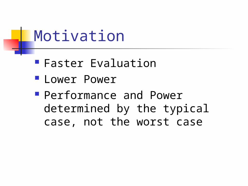
The Leakage Issue There is a only
one large “resistor”
Leakage current increases with technology
Solution? Introduce more large “resistors”
Rp
Rn
Precharge Eval
Leakage Paths without Sleep Mode
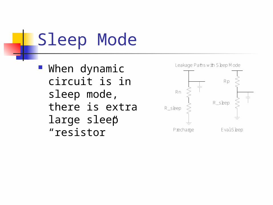
Sleep Mode When dynamic
circuit is in sleep mode, there is extra large sleep “resistor”
Rp
R_sleep
Rn
R_sleep
Precharge Eval-Sleep
Leakage Paths with Sleep Mode
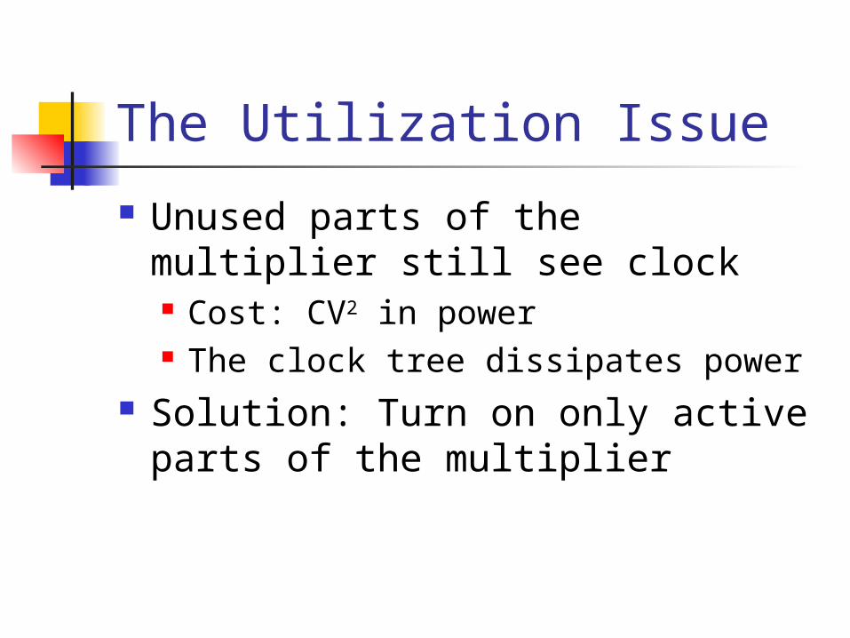
The Utilization Issue
Unused parts of the multiplier still see clock Cost: CV2 in power The clock tree dissipates power
Solution: Turn on only active parts of the multiplier
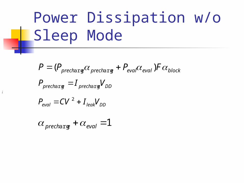
Power Dissipation w/o Sleep Mode
blockevalevaleprecheprech FPPP )( argarg
DDeprecheprech VIP argarg
DDleakeval VICVP 2
1arg evaleprech
;
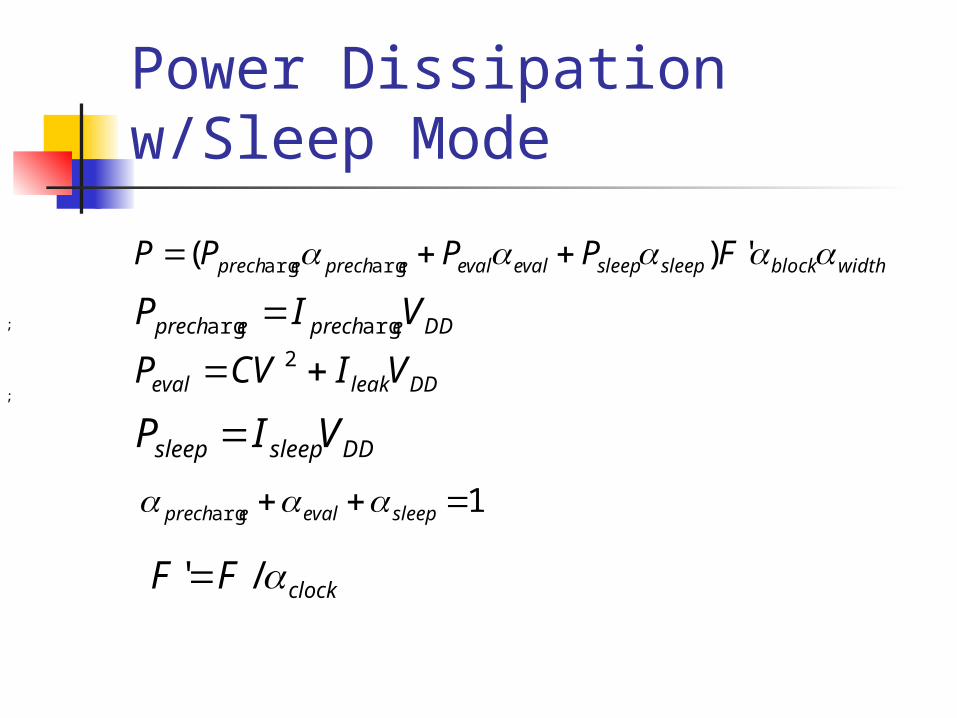
Power Dissipation w/Sleep Mode
widthblocksleepsleepevalevaleprecheprech FPPPP ')( argarg
DDeprecheprech VIP argarg
DDleakeval VICVP 2
DDsleepsleep VIP
1arg sleepevaleprech
clockFF /'
;
;
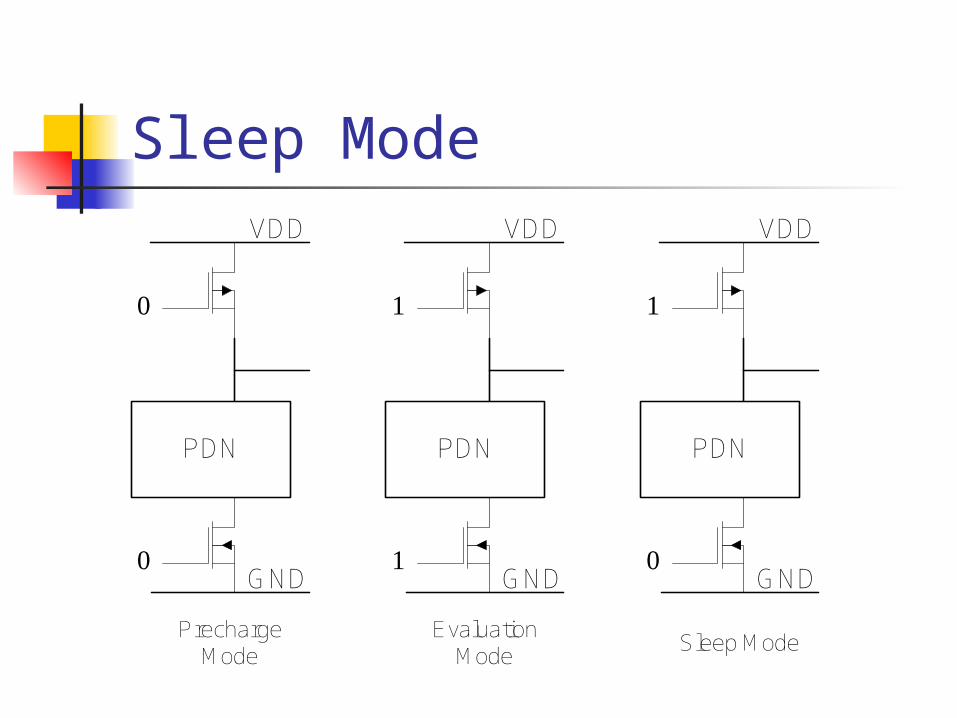
Sleep Mode
PDN
VDD
GND
0
0
PDN
VDD
GND
1
0
PDN
VDD
GND
1
1
Precharge Mode
Sleep ModeEvaluation
Mode
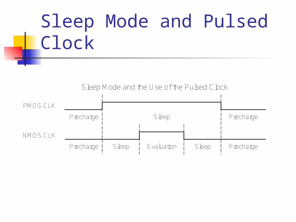
Sleep Mode and Pulsed Clock
PMOS CLK
NMOS CLK
Sleep Mode and the Use of the Pulsed Clock
Precharge
Precharge Sleep
Sleep
Evaluation Sleep Precharge
Precharge
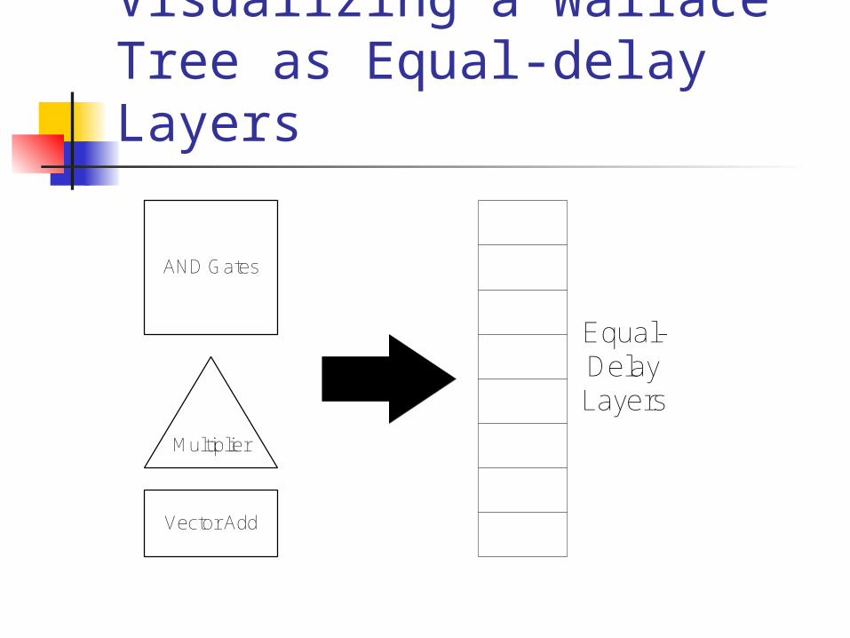
Visualizing a Wallace Tree as Equal-delay Layers
AND Gates
Vector Add
Multiplier
Equal- Delay Layers
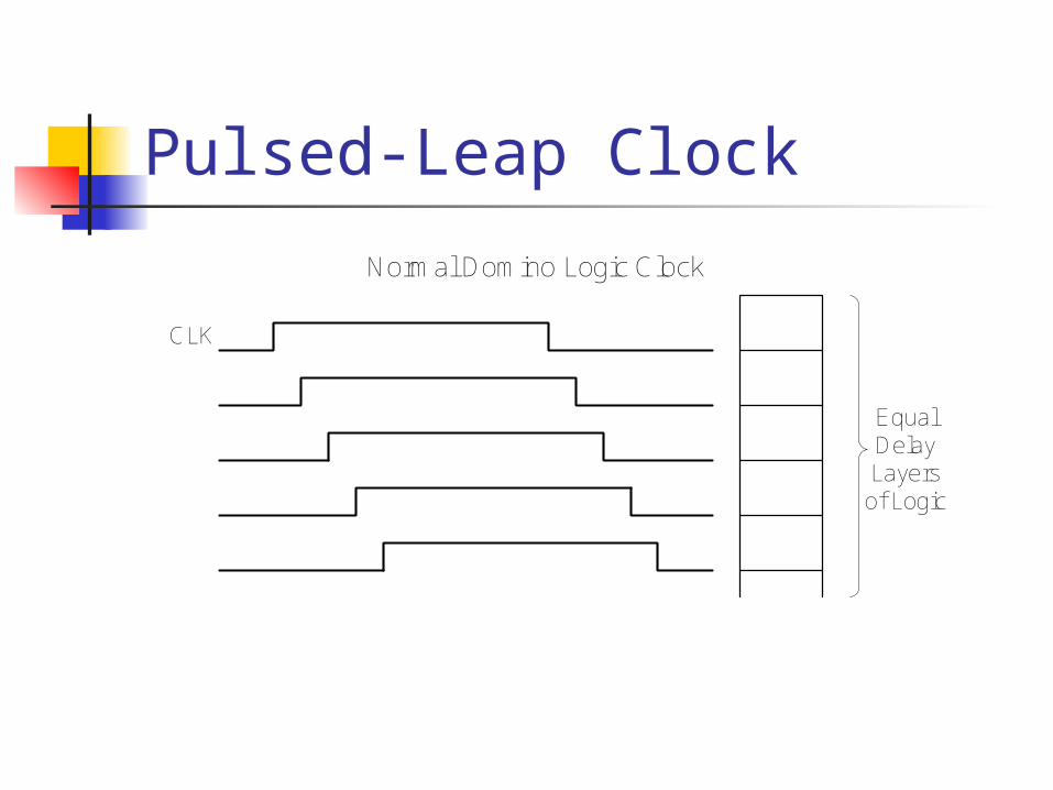
Pulsed-Leap Clock
Equal Delay Layers of Logic
CLK
Normal Domino Logic Clock
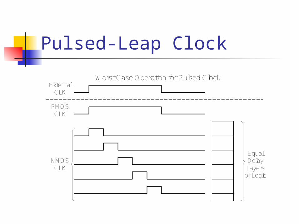
Pulsed-Leap Clock
Worst Case Operation for Pulsed Clock
Equal Delay Layers of Logic
NMOS CLK
PMOS CLK
External CLK
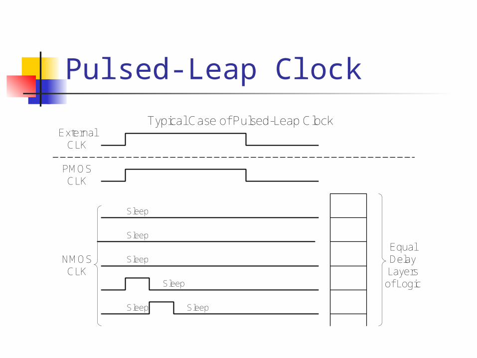
Pulsed-Leap Clock
External CLK
PMOS CLK
NMOS CLK
Typical Case of Pulsed-Leap Clock
Sleep
Sleep
SleepEqual Delay Layers of LogicSleep
SleepSleep
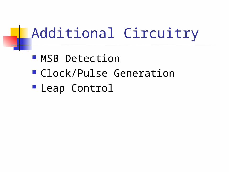
Additional Circuitry
MSB Detection Clock/Pulse Generation Leap Control
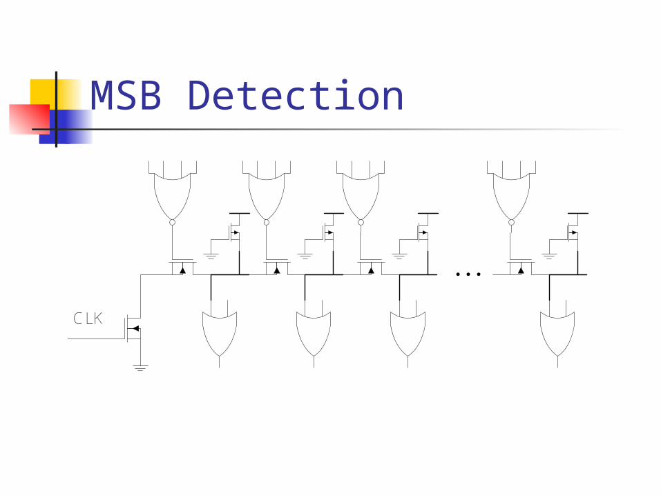
MSB Detection
. . .
CLK
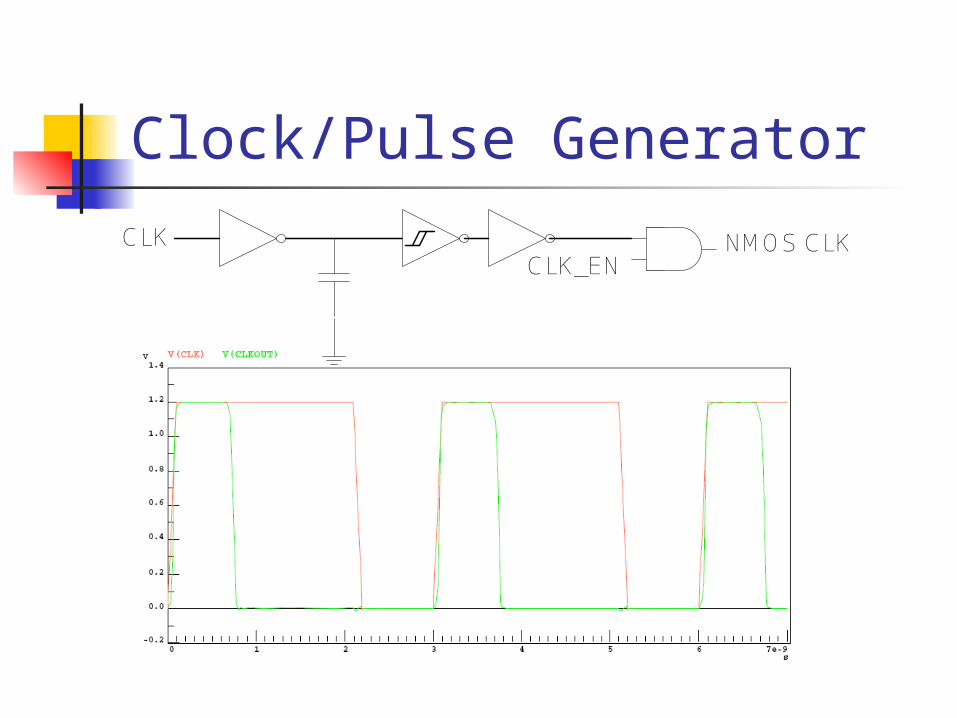
Clock/Pulse Generator
CLK_ENCLK NMOS CLK
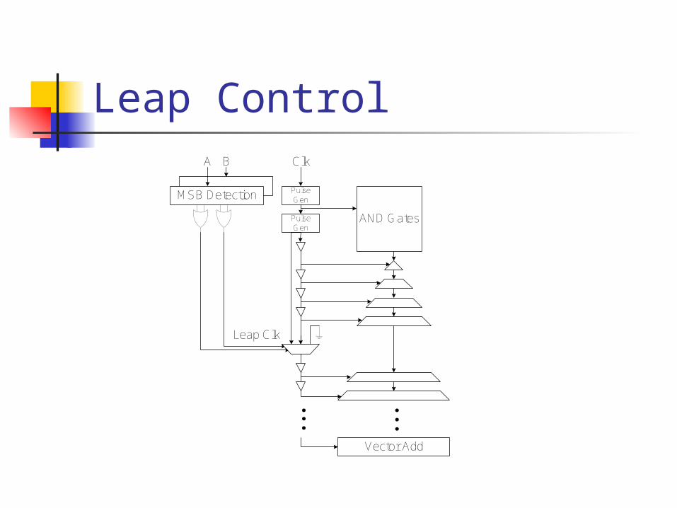
Leap Control
MSB Detection
A B
AND Gates
Vector Add
Pulse Gen
Pulse Gen
Clk
Leap Clk
......
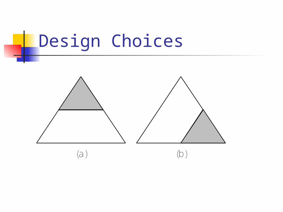
Design Choices
(a) (b)
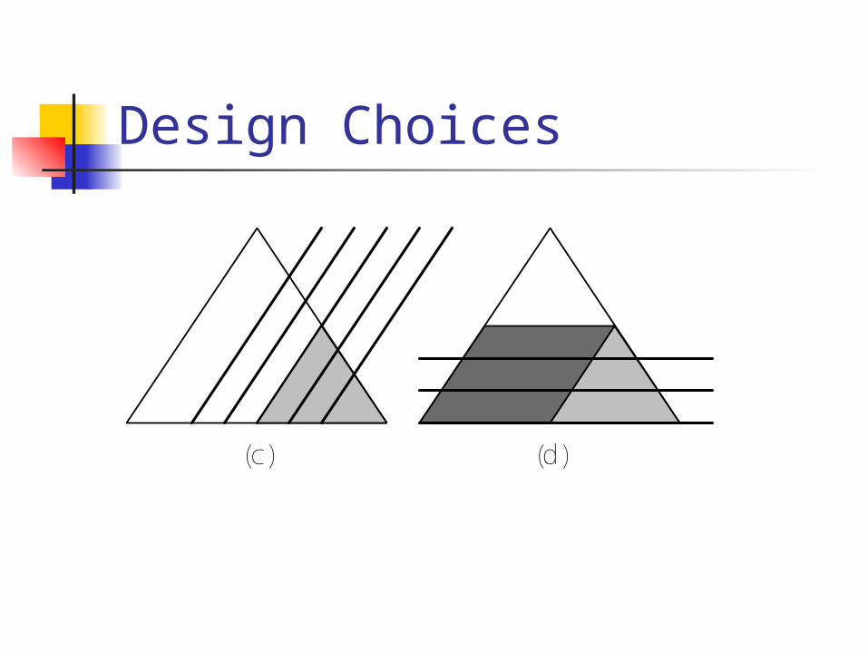
Design Choices
(c) (d)
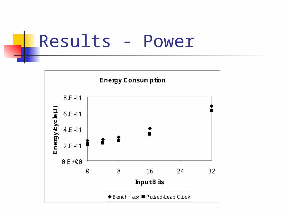
Results - Power
Energy Consumption
0.E+00
2.E-11
4.E-11
6.E-11
8.E-11
0 8 16 24 32
Input Bits
En
erg
y/c
yc
le(J
)
Benchmark Pulsed-Leap Clock
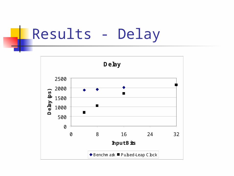
Results - Delay
Delay
0
500
1000
1500
2000
2500
0 8 16 24 32
Input Bits
De
lay
(p
s)
Benchmark Pulsed-Leap Clock
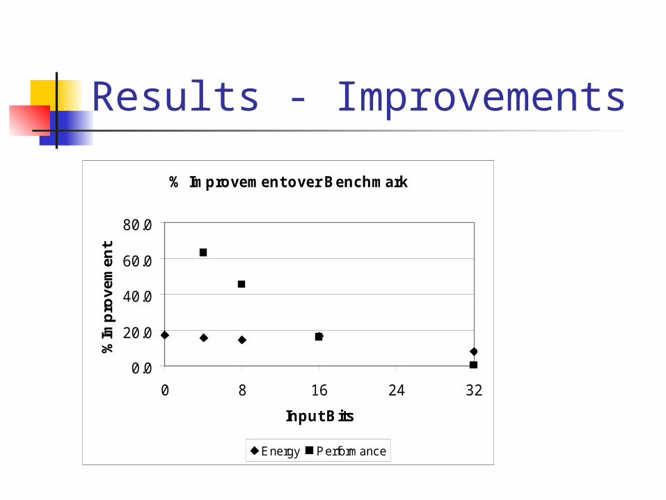
Results - Improvements
% Improvement over Benchmark
0.0
20.0
40.0
60.0
80.0
0 8 16 24 32
Input Bits
%Im
pro
ve
me
nt
Energy Performance
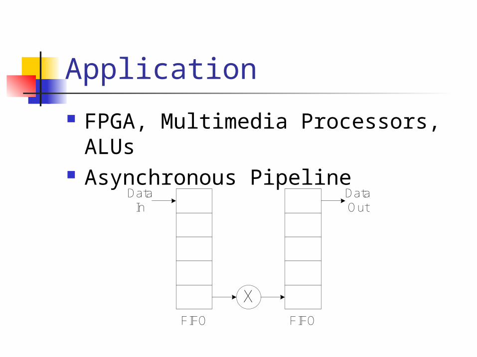
Application
FPGA, Multimedia Processors, ALUs Asynchronous Pipeline
XFIFO FIFO
Data In
Data Out