StratixGX FPGA Family - Altera · StratixGX FPGA Family ... and are designed for low power...
262
Altera Corporation 1 DS-STXGX-2.2 Preliminary Data Sheet Stratix GX FPGA Family Introduction The Stratix ® GX family of devices is Altera’s second FPGA family to combine high-speed serial transceivers with a scalable, high-performance logic array. Stratix GX devices include 4 to 20 high-speed transceiver channels, each incorporating clock data recovery (CDR) technology and embedded SERDES capability at data rates of up to 3.1875 gigabits per second (Gbps). These transceivers are grouped by four-channel transceiver blocks, and are designed for low power consumption and small die size. The Stratix GX FPGA technology is built upon the Stratix architecture, and offers a 1.5-V logic array with unmatched performance, flexibility, and time-to-market capabilities. This scalable, high-performance architecture makes Stratix GX devices ideal for high-speed backplane interface, chip-to-chip, and communications protocol-bridging applications. Features ■ Transceiver block features are as follows: ● High-speed serial transceiver channels with CDR provides 500-megabits per second (Mbps) to 3.1875-Gbps full-duplex operation ● Devices are available with 4, 8, 16, or 20 high-speed serial transceiver channels providing up to 127.5 Gbps of full-duplex serial bandwidth ● Support for transceiver-based protocols, including 10 Gigabit Ethernet attachment unit interface (XAUI), Gigabit Ethernet (GigE), and SONET/SDH ● Compatible with PCI Express, SMPTE 292M, Fibre Channel, and Serial RapidIO I/O standards ● Programmable differential output voltage (V OD ), pre-emphasis, and equalization settings for improved signal integrity ● Individual transmitter and receiver channel power-down capability implemented automatically by the Quartus ® II software for reduced power consumption during non-operation ● Programmable transceiver-to-FPGA interface with support for 8-, 10-, 16-, and 20-bit wide data paths ● 1.5-V pseudo current mode logic (PCML) for 500 Mbps to 3.1875 Gbps ● Support for LVDS, LVPECL, and 3.3-V PCML on reference clocks and receiver input pins (AC-coupled) ● Built-in self test (BIST) ● Hot insertion/removal protection circuitry December 2004, ver. 2.2
Transcript of StratixGX FPGA Family - Altera · StratixGX FPGA Family ... and are designed for low power...

Altera Corporation DS-STXGX-2.2
December 2004, ver. 2.2
Stratix GX FPGA Family
Data Sheet
Introduction The Stratix® GX family of devices is Altera’s second FPGA family to combine high-speed serial transceivers with a scalable, high-performance logic array. Stratix GX devices include 4 to 20 high-speed transceiver channels, each incorporating clock data recovery (CDR) technology and embedded SERDES capability at data rates of up to 3.1875 gigabits per second (Gbps). These transceivers are grouped by four-channel transceiver blocks, and are designed for low power consumption and small die size. The Stratix GX FPGA technology is built upon the Stratix architecture, and offers a 1.5-V logic array with unmatched performance, flexibility, and time-to-market capabilities. This scalable, high-performance architecture makes Stratix GX devices ideal for high-speed backplane interface, chip-to-chip, and communications protocol-bridging applications.
Features Transceiver block features are as follows: High-speed serial transceiver channels with CDR provides
500-megabits per second (Mbps) to 3.1875-Gbps full-duplex operation
Devices are available with 4, 8, 16, or 20 high-speed serial transceiver channels providing up to 127.5 Gbps of full-duplex serial bandwidth
Support for transceiver-based protocols, including 10 Gigabit Ethernet attachment unit interface (XAUI), Gigabit Ethernet (GigE), and SONET/SDH
Compatible with PCI Express, SMPTE 292M, Fibre Channel, and Serial RapidIO I/O standards
Programmable differential output voltage (VOD), pre-emphasis, and equalization settings for improved signal integrity
Individual transmitter and receiver channel power-down capability implemented automatically by the Quartus® II software for reduced power consumption during non-operation
Programmable transceiver-to-FPGA interface with support for 8-, 10-, 16-, and 20-bit wide data paths
1.5-V pseudo current mode logic (PCML) for 500 Mbps to 3.1875 Gbps
Support for LVDS, LVPECL, and 3.3-V PCML on reference clocks and receiver input pins (AC-coupled)
Built-in self test (BIST) Hot insertion/removal protection circuitry
1Preliminary

Stratix GX FPGA Family
Pattern detector and word aligner supports programmable patterns
8B/10B encoder/decoder performs 8- to 10-bit encoding and 10- to 8-bit decoding
Rate matcher compliant with IEEE 802.3-2002 for GigE mode and with IEEE 802-3ae for XAUI mode
Channel bonding compliant with IEEE 802.3ae (for XAUI mode only)
Device can bypass some transceiver block features if necessary
FPGA features are as follows: 10,570 to 41,250 logic elements (LEs); see Table 1 Up to 3,423,744 RAM bits (427,968 bytes) available without
reducing logic resources TriMatrix™ memory consisting of three RAM block sizes to
implement true dual-port memory and first-in-out (FIFO) buffers
Up to 16 global clock networks with up to 22 regional clock networks per device region
High-speed DSP blocks provide dedicated implementation of multipliers (faster than 300 MHz), multiply-accumulate functions, and finite impulse response (FIR) filters
Up to eight general usage phase-locked loops (four enhanced PLLs and four fast PLLs) per device provide spread spectrum, programmable bandwidth, clock switchover, real-time PLL reconfiguration, and advanced multiplication and phase shifting
Support for numerous single-ended and differential I/O standards
High-speed source-synchronous differential I/O support on up to 45 channels for 1-Gbps performance
Support for source-synchronous bus standards, including 10-Gigabit Ethernet XSBI, Parallel RapidIO, UTOPIA IV, Network Packet Streaming Interface (NPSI), HyperTransportTM technology, SPI-4 Phase 2 (POS-PHY Level 4), and SFI-4
Support for high-speed external memory, including zero bus turnaround (ZBT) SRAM, quad data rate (QDR and QDRII) SRAM, double data rate (DDR) SDRAM, DDR fast cycle RAM (FCRAM), and single data rate (SDR) SDRAM
Support for multiple intellectual property megafunctions from Altera® MegaCore® functions and Altera Megafunction Partners Program (AMPPSM) megafunctions
Support for remote configuration updates Dynamic phase alignment on LVDS receiver channels
2 Altera CorporationPreliminary

Features
Stratix GX devices are available in space-saving FineLine BGA® packages (refer to Tables 2 and 3), and in multiple speed grades (refer to Table 4). Stratix GX devices support vertical migration within the same package (that is, the designer can migrate between the EP1SGX10C and EP1SGX25C devices in the 672-pin FineLine BGA package). See the Stratix GX device pin tables for more information. Vertical migration means that designers can migrate to devices whose dedicated pins, configuration pins, and power pins are the same for a given package across device densities. For I/O pin migration across densities, the designer must cross-reference the available I/O pins using the device pin-outs for all planned densities of a given package type, to identify which I/O pins it is possible to migrate. The Quartus II software can automatically cross reference and place all pins for migration when given a device migration list.
Table 1. Stratix GX Device Features
Feature EP1SGX10CEP1SGX10D
EP1SGX25CEP1SGX25DEP1SGX25F
EP1SGX40DEP1SGX40G
LEs 10,570 25,660 41,250
Transceiver channels 4, 8 4, 8, 16 8, 20
Source-synchronous channels 22 39 45
M512 RAM blocks (32 × 18 bits) 94 224 384
M4K RAM blocks (128 × 36 bits) 60 138 183
M-RAM blocks (4K ×144 bits) 1 2 4
Total RAM bits 920,448 1,944,576 3,423,744
Digital signal processing (DSP) blocks 6 10 14
Embedded multipliers (1) 48 80 112
PLLs 4 4 8
Note to Table 1:(1) This parameter lists the total number of 9- × 9-bit multipliers for each device. For the total number of 18- × 18-bit
multipliers per device, divide the total number of 9- × 9-bit multipliers by 2. For the total number of 36- × 36-bit multipliers per device, decide the total number of 9- × 9-bit multipliers by 8.
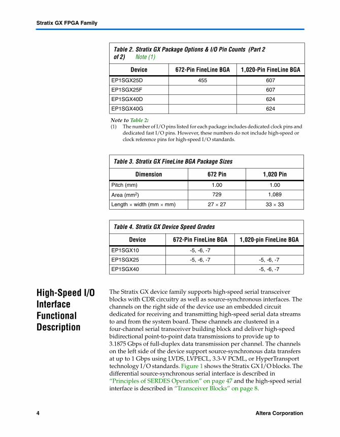
Table 2. Stratix GX Package Options & I/O Pin Counts (Part 1 of 2) Note (1)
Device 672-Pin FineLine BGA 1,020-Pin FineLine BGA
EP1SGX10C 362
EP1SGX10D 362
EP1SGX25C 455
Altera Corporation 3Preliminary
Stratix GX FPGA Family
High-Speed I/O Interface Functional Description
The Stratix GX device family supports high-speed serial transceiver blocks with CDR circuitry as well as source-synchronous interfaces. The channels on the right side of the device use an embedded circuit dedicated for receiving and transmitting high-speed serial data streams to and from the system board. These channels are clustered in a four-channel serial transceiver building block and deliver high-speed bidirectional point-to-point data transmissions to provide up to 3.1875 Gbps of full-duplex data transmission per channel. The channels on the left side of the device support source-synchronous data transfers at up to 1 Gbps using LVDS, LVPECL, 3.3-V PCML, or HyperTransport technology I/O standards. Figure 1 shows the Stratix GX I/O blocks. The differential source-synchronous serial interface is described in “Principles of SERDES Operation” on page 47 and the high-speed serial interface is described in “Transceiver Blocks” on page 8.
EP1SGX25D 455 607
EP1SGX25F 607
EP1SGX40D 624
EP1SGX40G 624
Note to Table 2:(1) The number of I/O pins listed for each package includes dedicated clock pins and
dedicated fast I/O pins. However, these numbers do not include high-speed or clock reference pins for high-speed I/O standards.
Table 3. Stratix GX FineLine BGA Package Sizes
Dimension 672 Pin 1,020 Pin
Pitch (mm) 1.00 1.00
Area (mm2) 729 1,089
Length × width (mm × mm) 27 × 27 33 × 33
Table 4. Stratix GX Device Speed Grades
Device 672-Pin FineLine BGA 1,020-pin FineLine BGA
EP1SGX10 -5, -6, -7
EP1SGX25 -5, -6, -7 -5, -6, -7
EP1SGX40 -5, -6, -7
Table 2. Stratix GX Package Options & I/O Pin Counts (Part 2 of 2) Note (1)
Device 672-Pin FineLine BGA 1,020-Pin FineLine BGA
4 Altera CorporationPreliminary

FPGA Functional Description
Figure 1. Stratix GX I/O Blocks Note (1)
Notes to Figure 1:(1) Figure 1 is a top view of the Stratix GX silicon die.(2) Banks 9 through 12 are enhanced PLL external clock output banks.(3) If the high-speed differential I/O pins are not used for high-speed differential signaling, they can support all of the
I/O standards except HSTL class I and II, GTL, SSTL-18 Class II, PCI, PCI-X, and AGP 1×/2×.(4) For guidelines for placing single-ended I/O pads next to differential I/O pads, see the Selectable I/O Standards in
Stratix & Stratix GX Devices chapter in the Stratix Device Handbook, Volume 2.(5) These I/O banks in Stratix GX devices also support the LVDS, LVPECL, and 3.3-V PCML I/O standards on reference
clocks and receiver input pins (AC coupled).
FPGA Functional Description
Stratix GX devices contain a two-dimensional row- and column-based architecture to implement custom logic. A series of column and row interconnects of varying length and speed provide signal interconnects between logic array blocks (LABs), memory block structures, and DSP blocks.
LVDS, LVPECL, 3.3-V PCML, and HyperTransport I/O Blockand Regular I/O Pins (3)
I/O Banks 3, 4, 9 & 10 Support All Single-Ended I/O Standards (2)
I/O Banks 7, 8, 11 & 12 Support All Single-Ended I/O Standards (2)
I/O Banks 1 and 2 Support AllSingle-Ended I/O Standards Except Differential HSTL Output Clocks, Differential SSTL-2 Output Clocks, HSTL Class II, GTL, SSTL-18 Class II, PCI, PCI-X, and AGP 1×/2×
DQST9 DQST8 DQST7 DQST6 DQST5 DQST4 DQST3 DQST2 DQST1 DQST0PLL5
VREF1B3 VREF2B3 VREF3B3 VREF4B3 VREF5B3 VREF1B4 VREF2B4 VREF3B4 VREF4B4 VREF5B4
VREF5B8 VREF4B8 VREF3B8 VREF2B8 VREF1B8 VREF5B7 VREF4B7 VREF3B7 VREF2B7 VREF1B7PLL6
DQSB9 DQSB8 DQSB7 DQSB6 DQSB5 DQSB4 DQSB3 DQSB2 DQSB1 DQSB0
9 10
VR
EF
1B2
VR
EF
2B2
VR
EF
3B2
VR
EF
4B2
VR
EF
1B1
VR
EF
2B1
VR
EF
3B1
VR
EF
4B1
PLL1
PLL2
Ban
k 1
Ban
k 2
Bank 3 Bank 4
11 12Bank 8 Bank 7
LVDS, LVPECL, 3.3-V PCML, and HyperTransport I/O Block
and Regular I/O Pins (3)
PLL7
PLL8 PLL12
PLL11
(4)
(4)
I/O Bank 13 (5)
I/O Bank 14 (5)
I/O Bank 17 (5)
I/O Bank 16 (5)
I/O Bank 15 (5)
1.5-V PCML (5)
Altera Corporation 5Preliminary
Stratix GX FPGA Family
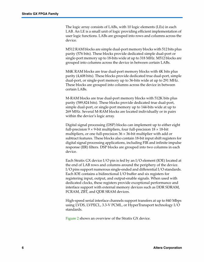
The logic array consists of LABs, with 10 logic elements (LEs) in each LAB. An LE is a small unit of logic providing efficient implementation of user logic functions. LABs are grouped into rows and columns across the device.
M512 RAM blocks are simple dual-port memory blocks with 512 bits plus parity (576 bits). These blocks provide dedicated simple dual-port or single-port memory up to 18-bits wide at up to 318 MHz. M512 blocks are grouped into columns across the device in between certain LABs.
M4K RAM blocks are true dual-port memory blocks with 4K bits plus parity (4,608 bits). These blocks provide dedicated true dual-port, simple dual-port, or single-port memory up to 36-bits wide at up to 291 MHz. These blocks are grouped into columns across the device in between certain LABs.
M-RAM blocks are true dual-port memory blocks with 512K bits plus parity (589,824 bits). These blocks provide dedicated true dual-port, simple dual-port, or single-port memory up to 144-bits wide at up to 269 MHz. Several M-RAM blocks are located individually or in pairs within the device’s logic array.
Digital signal processing (DSP) blocks can implement up to either eight full-precision 9 × 9-bit multipliers, four full-precision 18 × 18-bit multipliers, or one full-precision 36 × 36-bit multiplier with add or subtract features. These blocks also contain 18-bit input shift registers for digital signal processing applications, including FIR and infinite impulse response (IIR) filters. DSP blocks are grouped into two columns in each device.
Each Stratix GX device I/O pin is fed by an I/O element (IOE) located at the end of LAB rows and columns around the periphery of the device. I/O pins support numerous single-ended and differential I/O standards. Each IOE contains a bidirectional I/O buffer and six registers for registering input, output, and output-enable signals. When used with dedicated clocks, these registers provide exceptional performance and interface support with external memory devices such as DDR SDRAM, FCRAM, ZBT, and QDR SRAM devices.
High-speed serial interface channels support transfers at up to 840 Mbps using LVDS, LVPECL, 3.3-V PCML, or HyperTransport technology I/O standards.
Figure 2 shows an overview of the Stratix GX device.
6 Altera CorporationPreliminary
FPGA Functional Description
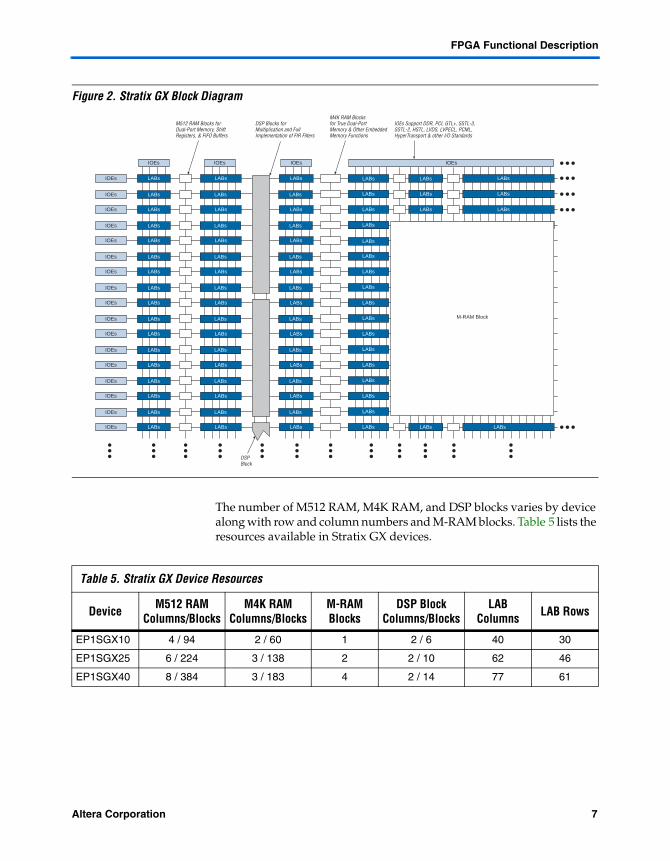
Figure 2. Stratix GX Block Diagram
The number of M512 RAM, M4K RAM, and DSP blocks varies by device along with row and column numbers and M-RAM blocks. Table 5 lists the resources available in Stratix GX devices.
M512 RAM Blocks for Dual-Port Memory, Shift Registers, & FIFO Buffers
DSP Blocks forMultiplication and FullImplementation of FIR Filters
M4K RAM Blocksfor True Dual-Port Memory & Other EmbeddedMemory Functions
IOEs Support DDR, PCI, GTL+, SSTL-3, SSTL-2, HSTL, LVDS, LVPECL, PCML, HyperTransport & other I/O Standards
IOEs
IOEs
IOEs
IOEs
IOEs
IOEs
IOEs
IOEs
IOEs
IOEs
IOEs
IOEs
IOEs
IOEs
IOEs
IOEs
IOEs
LABs
LABs
IOEs
LABs
LABs
LABs
LABs
LABs
LABs
LABs
LABs
LABs
LABs
LABs
LABs
LABs
LABs
LABs
LABs
LABs
IOEs
LABs
LABs
LABs
LABs
LABs
LABs
LABs
LABs
LABs
LABs
LABs
LABs
LABs
LABs
LABs
LABs LABs
LABs
IOEs IOEs
LABs
LABs LABs
LABs LABs
LABs
LABs
LABs
LABs
LABs
LABs
LABs
LABs
LABs
LABs
LABs
LABs
LABs
LABs
LABs LABs
LABs
LABs
LABs
LABs
LABs
LABs
LABs
LABs
LABs
LABs
LABs
LABs
LABs
LABs
LABs
LABs
LABs
LABs
LABs
LABs
DSPBlock
M-RAM Block
Table 5. Stratix GX Device Resources
Device M512 RAM Columns/Blocks
M4K RAM Columns/Blocks
M-RAM Blocks
DSP Block Columns/Blocks
LAB Columns LAB Rows
EP1SGX10 4 / 94 2 / 60 1 2 / 6 40 30
EP1SGX25 6 / 224 3 / 138 2 2 / 10 62 46
EP1SGX40 8 / 384 3 / 183 4 2 / 14 77 61
Altera Corporation 7Preliminary
Stratix GX FPGA Family
Transceiver Blocks
Stratix GX devices incorporate dedicated embedded circuitry on the right side of the device, which contains up to 20 high-speed 3.1875-Gbps serial transceiver channels. Each Stratix GX transceiver block contains four full-duplex channels and supporting logic to transmit and receive high-speed serial data streams. The transceiver block uses the channels to deliver bidirectional point-to-point data transmissions with up to 3.1875 Gbps of data transition per channel.
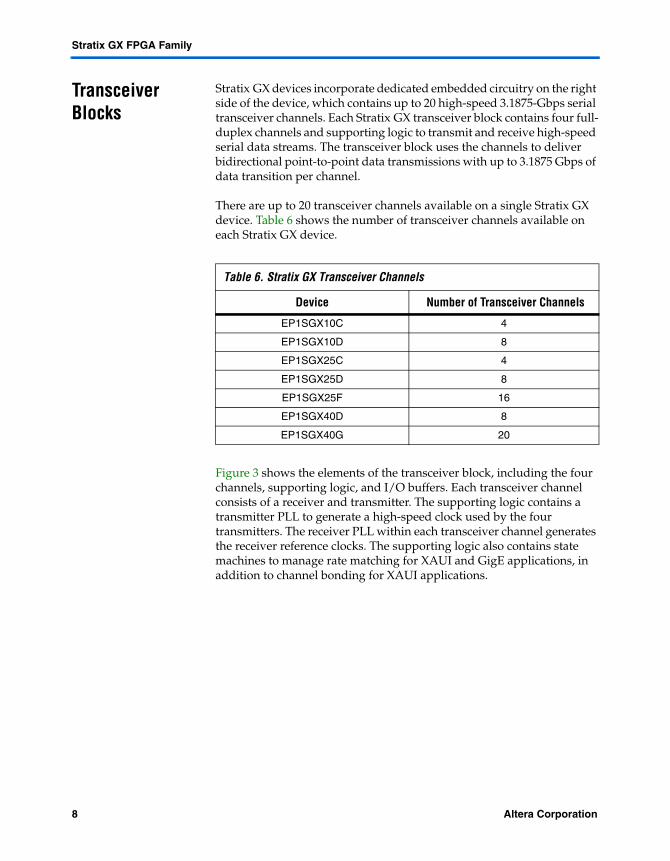
There are up to 20 transceiver channels available on a single Stratix GX device. Table 6 shows the number of transceiver channels available on each Stratix GX device.
Figure 3 shows the elements of the transceiver block, including the four channels, supporting logic, and I/O buffers. Each transceiver channel consists of a receiver and transmitter. The supporting logic contains a transmitter PLL to generate a high-speed clock used by the four transmitters. The receiver PLL within each transceiver channel generates the receiver reference clocks. The supporting logic also contains state machines to manage rate matching for XAUI and GigE applications, in addition to channel bonding for XAUI applications.
Table 6. Stratix GX Transceiver Channels
Device Number of Transceiver Channels
EP1SGX10C 4
EP1SGX10D 8
EP1SGX25C 4
EP1SGX25D 8
EP1SGX25F 16
EP1SGX40D 8
EP1SGX40G 20
8 Altera CorporationPreliminary

Transceiver Blocks
Figure 3. Stratix GX Transceiver Block
Channel 0
Receiver Channel 0
Transmitter Channel 0
Receiver Pins
Transmitter Pins
Channel 1
Receiver Channel 1
Transmitter Channel 1
Receiver Pins
Transmitter Pins
XAUIReceiver
StateMachine
TransmitterPLL
XAUITransmitter
StateMachine
ChannelAlignerState
Machine
Receiver Pins
Transmitter Pins
Receiver Pins
Transmitter Pins
PLDLogicArray
PLDLogicArray
PLDLogicArray
PLDLogicArray
PLDLogicArray
PLDLogicArray
Channel 2
Receiver Channel 2
Transmitter Channel 2
Channel 3
Receiver Channel 3
Transmitter Channel 3
Altera Corporation 9Preliminary
Stratix GX FPGA Family
Each Stratix GX transceiver channel consists of a transmitter and receiver. The transmitter contains the following:
Transmitter PLL Transmitter phase compensation FIFO buffer Byte serializer 8B/10B encoder Serializer (parallel to serial converter) Transmitter output buffer
The receiver contains the following:
Input buffer Clock recovery unit (CRU) Deserializer Pattern detector and word aligner Rate matcher and channel aligner 8B/10B decoder Receiver logic array interface
Designers can set all the Stratix GX transceiver functions through the Quartus II software. Designers can set programmable pre-emphasis, programmable equalizer, and programmable VOD dynamically as well. Each Stratix GX transceiver channel is also capable of BIST generation and verification in addition to various loopback modes. Figure 4 shows the block diagram for the Stratix GX transceiver channel.
Stratix GX transceivers provide physical coding sublayer (PCS) and physical media attachment (PMA) implementation for protocols such as 10-gigabit XAUI and GigE. The PCS portion of the transceiver consists of the logic array interface, 8B/10B encoder/decoder, pattern detector, word aligner, rate matcher, channel aligner, and the BIST and pseudo-random binary sequence pattern generator/verifier. The PMA portion of the transceiver consists of the serializer/deserializer, the CRU, and the I/O buffers.
10 Altera CorporationPreliminary

Transceiver Blocks
Figure 4. Stratix GX Transceiver Channel Note (1)
Note to Figure 4: (1) There are four transciever channels in a transceiver block.
Des
eria
lizer
Des
eria
lizer
Rec
eive
rP
LL
Tran
smitt
erP
LL
Clo
ckR
ecov
ery
Uni
t
Wor
dA
ligne
r
Cha
nnel
Alig
ner
Rat
eM
atch
er8B
/10B
Dec
oder
Byt
eD
eser
ializ
er
Pha
seC
ompe
nsat
ion
FIF
O
8B/1
0BE
ncod
er
Byt
eS
eria
lizer
Ref
eren
ceC
lock
Pha
seC
ompe
nsat
ion
FIF
O
Rec
eive
r
Tran
smitt
er
Cha
nnel
0
To C
hann
els
1-3
Altera Corporation 11Preliminary

Stratix GX FPGA Family
Transmitter Path
This section describes the data path through the Stratix GX transmitter (see Figure 4). Data travels through the Stratix GX transmitter via the following modules:
Transmitter PLL Transmitter phase compensation FIFO buffer Byte serializer 8B/10B encoder Serializer (parallel to serial converter) Transmitter output buffer
Transmitter PLL
Each transceiver block has one transmitter PLL, which receives the reference clock and generates the following signals:
High-speed serial clock used by the serializer Slow-speed reference clock used by the receiver Slow-speed clock used by the logic array (divisible by two for
double-width mode)
The INCLK clock is the input into the transmitter PLL. There is one INCLK clock per transceiver block. This clock can be fed by either the REFCLKB pin, PLD routing, or the inter-transceiver routing line. See the section “Stratix GX Clocking” on page 36 for more information about the inter-transceiver lines.
The transmitter PLL in each transceiver block clocks the circuits in the transmit path. The transmitter PLL is also used to train the receiver PLL. If no transmit channels are used in the transceiver block, the transmitter PLL can be turned off. Figure 5 is a block diagram of the transmitter PLL.
Figure 5. Transmitter PLL Block Diagram Note (1)
Note to Figure 5:(1) The divider in the PLL divides by 4, 8, 10, 16, or 20.
Inter Quad Routing (IQ1)Inter Quad Routing (IQ2)Global Clks, IO Bus, Gen Routing
DedicatedLocalREFCLKB
÷2
INCLKCharge Pump +Loop Filter
ClockDriver
÷m
Up
Down
High Speed Clock
Low Speed Clock
VCOPFD
12 Altera CorporationPreliminary

Transceiver Blocks
The transmitter PLL can support up to 3.1875 Mbps. The input clock frequency for –5 and –6 speed grade devices is limited to 650 MHz if designers use the REFCLKB pin or to 325 MHz if designers use the other clock routing resources. For –7 speed grade devices, the maximum input clock frequency is 312.5 MHz with the REFCLKB pin, and the maximum is 156.25 MHz for all other clock routing resources. An optional PLL_LOCKED port is available to indicate whether the transmitter PLL is locked to the reference clock. The transmitter PLL has a programmable loop bandwidth that can be set to low or high. The loop bandwidth parameter can be statically set in the Quartus II software.
Table 7 lists the adjustable parameters in the transmitter PLL.
Transmitter Phase Compensation FIFO Buffer
The transmitter phase compensation FIFO buffer resides in the transceiver block at the PLD boundary. This FIFO buffer compensates for the phase differences between the transmitter reference clock (inclk) and the PLD interface clock (tx_coreclk). The phase difference between the two clocks must be less than 360°. The PLD interface clock must also be frequency locked to the transmitter reference clock. The phase compensation FIFO buffer is four words deep and cannot be bypassed.
Byte Serializer
The byte serializer takes double-width words (16 or 20 bits) from the PLD interface and converts them to a single width word (8 or 10 bits) for use in the transceiver. The transmit data path after the byte serializer is single width (8 or 10 bits). The byte serializer is bypassed when single width mode (8 or 10 bits) is used at the PLD interface.
Table 7. Transmitter PLL Specifications
Parameter Specifications
Input reference frequency range 25 MHz to 650 MHz
Data rate support 500 Mbps to 3.1875 Gbps
Multiplication factor (W) 2, 4, 5, 8, 10, 16, or 20 (1)
Bandwidth Low, high
Note to Table 7:(1) Multiplication factors 2 and 5 can only be achieved with the use of the pre-divider
on the REFCLKB pin.
Altera Corporation 13Preliminary
Stratix GX FPGA Family
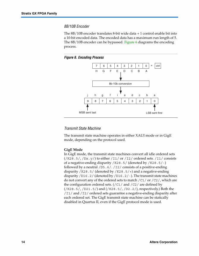
8B/10B Encoder
The 8B/10B encoder translates 8-bit wide data + 1 control enable bit into a 10-bit encoded data. The encoded data has a maximum run length of 5. The 8B/10B encoder can be bypassed. Figure 6 diagrams the encoding process.
Figure 6. Encoding Process
Transmit State Machine
The transmit state machine operates in either XAUI mode or in GigE mode, depending on the protocol used.
GigE ModeIn GigE mode, the transmit state machines convert all idle ordered sets (/K28.5/, /Dx.y/) to either /I1/ or /I2/ ordered sets. /I1/ consists of a negative-ending disparity /K28.5/ (denoted by /K28.5/-) followed by a neutral /D5.6/. /I2/ consists of a positive-ending disparity /K28.5/ (denoted by /K28.5/+) and a negative-ending disparity /D16.2/ (denoted by /D16.2/-). The transmit state machines do not convert any of the ordered sets to match /C1/ or /C2/, which are the configuration ordered sets. (/C1/ and /C2/ are defined by (/K28.5/, /D21.5/) and (/K28.5/, /D2.2/), respectively.) Both the /I1/ and /I2/ ordered sets guarantee a negative-ending disparity after each ordered set. The GigE transmit state machine can be statically disabled in Quartus II, even if the GigE protocol mode is used.
9 8 7 6 5 4 3 2 1 0
8b-10b conversion
7 6 5 4 3 2 1 0
H G F E D C B A
+ ctrl
j h g f i e d c b a
MSB sent last LSB sent first
14 Altera CorporationPreliminary
Transceiver Blocks
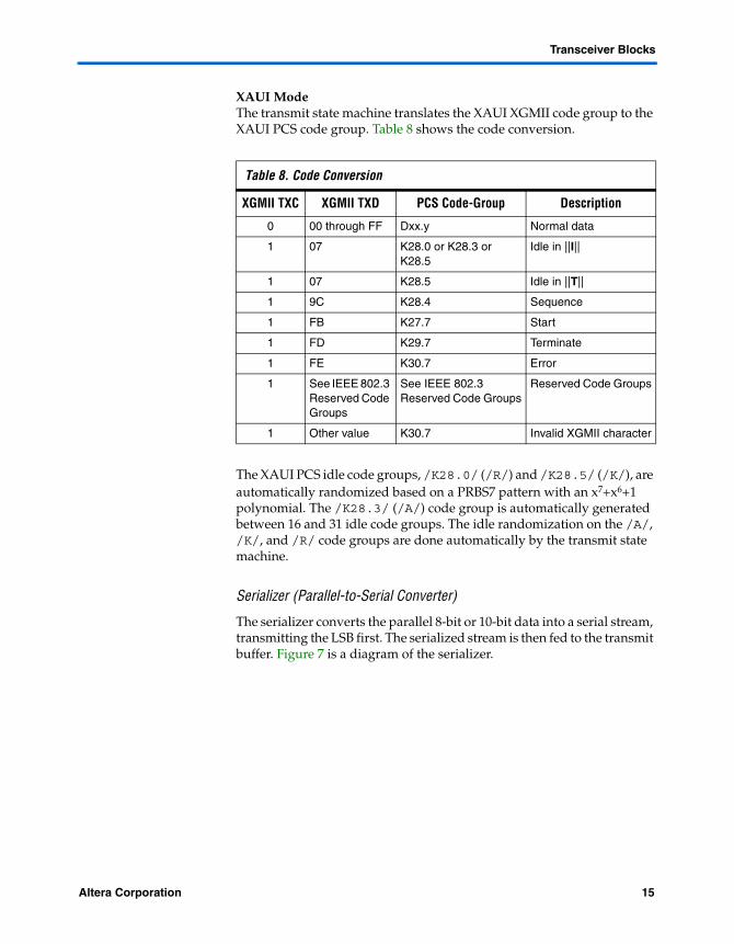
XAUI ModeThe transmit state machine translates the XAUI XGMII code group to the XAUI PCS code group. Table 8 shows the code conversion.
The XAUI PCS idle code groups, /K28.0/ (/R/) and /K28.5/ (/K/), are automatically randomized based on a PRBS7 pattern with an x7+x6+1 polynomial. The /K28.3/ (/A/) code group is automatically generated between 16 and 31 idle code groups. The idle randomization on the /A/, /K/, and /R/ code groups are done automatically by the transmit state machine.
Serializer (Parallel-to-Serial Converter)
The serializer converts the parallel 8-bit or 10-bit data into a serial stream, transmitting the LSB first. The serialized stream is then fed to the transmit buffer. Figure 7 is a diagram of the serializer.
Table 8. Code Conversion
XGMII TXC XGMII TXD PCS Code-Group Description
0 00 through FF Dxx.y Normal data
1 07 K28.0 or K28.3 or K28.5
Idle in ||I||
1 07 K28.5 Idle in ||T||
1 9C K28.4 Sequence
1 FB K27.7 Start
1 FD K29.7 Terminate
1 FE K30.7 Error
1 See IEEE 802.3 Reserved Code Groups
See IEEE 802.3 Reserved Code Groups
Reserved Code Groups
1 Other value K30.7 Invalid XGMII character
Altera Corporation 15Preliminary

Stratix GX FPGA Family
Figure 7. Serializer
Transmit Buffer
The Stratix GX transceiver buffers support the 1.5-V pseudo current mode logic (PCML) I/O standard at a rate up to 3.1875 Gbps, across up to 40 inches of FR4 trace, and across 2 connectors. Additional I/O standards, LVDS, 3.3-V PCML, LVPECL, can be supported when AC coupled. The common mode of the Output Driver is 750 mV.
The output buffer, as shown in Figure 8, consists of a programmable output driver and a programmable pre-emphasis circuit.
D7
D6
D5
D4
D3
D2
D1
D0
D7
D6
D5
D4
D3
D2
D1
D0
Low-speedparallel clock
High-speedserial clock
Serial dataout (to outputbuffer)
D8
D9
D8
D9
10
16 Altera CorporationPreliminary

Transceiver Blocks
Figure 8. Output Buffer
Programmable Output DriverThe programmable output driver can be set to drive out 400 to 1,600 mV. Table 9 shows the available settings for each termination value. The VOD can be dynamically or statically set. The output driver requires either internal or external termination at the source.
Table 9. Programmable VOD (Differential) Note (1)
Termination Setting (Ω) VO D Setting (mV)
100 400, 800, 1000, 1200, 1400, 1600
120 480, 960, 1200, 1440
150 600, 1200, 1500
Note to Table 9:(1) VOD differential is measured as VA – VB (see Figure 9).
Serializer
ProgrammableTermination
ProgrammablePre-Emphasis
Output Buffer
OutputPinsProgrammable
OutputDriver
Altera Corporation 17Preliminary
Stratix GX FPGA Family
Figure 9. VOD Differential
Programmable Pre-EmphasisThe programmable pre-emphasis module controls the output driver to boost the high frequency components, to compensate for losses in the transmission medium, as shown in Figure 10. The pre-emphasis can be dynamically or statically set. There are five possible pre-emphasis settings (1 through 5), with 5 being the highest and 0 being no pre-emphasis.
Figure 10. Programmable Pre-Emphasis Model
Pre-emphasis percentage is defined as VPP/VS – 1, where VPP is the differential emphasized voltage (peak-to-peak) and VS is the differential steady-state voltage (peak-to-peak).
Single-Ended Waveform
Differential Waveform
VA
VB
±VOD
+VOD
− VOD
VOCM − VOD (Differential) = VA − VB
VOD (Differential)
VOCM
VA VB−
2
VOCM + VA VB−
2
VCM VPP(p-p)VS(p-p)
BitTime
VPP
BitTime
VS
18 Altera CorporationPreliminary

Transceiver Blocks
Programmable Transmitter TerminationThe programmable termination can be statically set in the Quartus II software. The values are 100 Ω, 120 Ω, 150 Ω, and off. Figure 11 shows the setup for programmable termination.
Figure 11. Programmable Transmitter Termination
Receiver Path
This section describes the data path through the Stratix GX receiver (refer to Figure 4 on page 11). Data travels through the Stratix GX receiver via the following modules:
Input buffer Clock Recovery Unit (CRU) Deserializer Pattern detector and word aligner Rate matcher and channel aligner 8B/10B decoder Receiver logic array interface
Receiver Input Buffer
The Stratix GX receiver input buffer supports the 1.5-V PCML I/O standard at a rate up to 3.1875 Gbps. Additional I/O standards, LVDS, 3.3-V PCML, and LVPECL can be supported when AC coupled. The common mode of the input buffer is 1.1 V. The receiver can support Stratix GX-to-Stratix GX DC coupling.
Figure 12 shows a diagram of the receiver input buffer, which contains:
Programmable termination Programmable equalizer
ProgrammableOutputDriver
50, 60, or 75 ΩVCM
Altera Corporation 19Preliminary

Stratix GX FPGA Family
Figure 12. Receiver Input Buffer
Programmable TerminationThe programmable termination can be statically set in the Quartus II software. Figure 13 shows the setup for programmable receiver termination.
Figure 13. Programmable Receiver Termination
If external termination is used, then the receiver must be externally terminated and biased to 1.1 V. Figure 14 shows an example of an external termination/biasing circuit.
ProgrammableTermination
InputPins
DifferentialInputBuffer
ProgrammableEqualizer
DifferentialInputBuffer50, 60, or 75 Ω
50, 60, or 75 Ω
VCM
20 Altera CorporationPreliminary
Transceiver Blocks
Figure 14. External Termination & Biasing Circuit
Programmable Equalizer
The programmable equalizer module boosts the high frequency components of the incoming signal to compensate for losses in the transmission medium. There are five possible equalization settings (0, 1, 2, 3, 4) to compensate for 0”, 10”, 20”, 30”, and 40” of FR4 trace. These settings should be interpreted loosely. The programmable equalizer can be set dynamically or statically.
Receiver PLL & CRU
Each transceiver block has four receiver PLLs and CRUs, each of which is dedicated to a receive channel. If the receive channel associated with a particular receiver PLL or CRU is not used, then the receiver PLL or CRU is powered down for the channel. Figure 15 is a diagram of the receiver PLL and CRU circuits.
TransmissionLine
C1
R1/R2 = 1KVDD × R2/(R1 + R 2) = 1.1 V
50/60/75-ΩTerminationResistance
R1
R2
VDD
Receiver External Termination and Biasing
Stratix GX Device
Receiver External Termination and Biasing
RXIP
RXIN
Receiver
Altera Corporation 21Preliminary

Stratix GX FPGA Family
Figure 15. Receiver PLL & CRU Circuit
Note to Figure 15:(1) m = 8, 10 16, or 20.
The receiver PLLs and CRUs are capable of supporting up to 3.1875 Gbps. The input clock frequency for –5 and –6 speed grade devices is limited to 650 MHz if designers use the REFCLKB pin or 325 MHz if designers use the other clock routing resources. The maximum input clock frequency for –7 speed grade devices is 312.5 MHz if designers use the REFCLKB pin or 156.25 MHz with the other clock routing resources. An optional RX_LOCKED port (active low signal) is available to indicate whether the PLL is locked to the reference clock. The receiver PLL has a programmable loop bandwidth, which can be set to low, medium, or high. The loop bandwidth parameter can be statically set by the Quartus II software.
DedicatedLocalREFCLKB
÷ 2
PFD
VCO
÷ m (1)
Charge Pump and Loop Filter
rx_riv[ ]CRU
Global Clks, IO Bus, Gen Routing
rx_locktorefclk
rx_locktodata
RX_IN
rx_freqlocked[]
High-speed RCVD_CLK
Low-speed RCVD_CLK
Low-Speed TX_PLL_CLK
RX CRUCLK
updown
updown
Receiver PLL
Inter Transceiver Routing (IQ1)
rx_locked
22 Altera CorporationPreliminary
Transceiver Blocks
Table 10 lists the adjustable parameters of the receiver PLL and CRU. All the parameters listed are statically programmable in the Quartus II software.
The CRU has a built-in switchover circuit to select whether the voltage-controlled oscillator of the PLL is trained by the reference clock or the data. The optional port rx_freqlocked can be used to monitor when the CRU is in locked to data mode.
In the automatic mode, the following conditions must be met for the CRU to switch from locked to reference to locked to data mode:
The CRU PLL is within the prescribed PPM frequency threshold setting (125 PPM, 250 PPM, 500 PPM, 1,000 PPM) of the CRU reference clock.
The reference clock and CRU PLL output are phase matched (phases are within .08 UI).
The automatic switchover circuit can be overridden by using the optional ports rx_lockedtorefclk and rx_locktodata. Table 11 shows the possible combinations of these two signals.
If the rx_lockedtorefclk and rx_locktodata ports are not used, the default is auto mode.
Table 10. Receiver PLL & CRU Adjustable Parameters
Parameter Specifications
Input reference frequency range 25 MHz to 650 MHz
Data rate support 500 Mbps to 3.1875 Gbps
Multiplication factor (W) 2, 4, 5, 8, 10, 16, or 20 (1)
PPM detector 125, 250, 500, 1,000
Bandwidth Low, medium, high
Run length detector 10-bit or 20-bit mode: 5 to 160 in steps of 5
8-bit or 16-bit mode: 4 to 128 in steps of 4
Note to Table 10:(1) Multiplication factors 2, 4, and 5 can only be achieved with the use of the pre-
divider on the REFCLKB port or if the CRU is trained with the low speed clock from the transmitter PLL.
Altera Corporation 23Preliminary

Stratix GX FPGA Family
Deserializer (Serial-to-Parallel Converter)
The deserializer converts the serial stream into a parallel 8- or 10-bit data bus. The deserializer receives the least significant bit first. Figure 16 is a diagram of the deserializer.
Figure 16. Deserializer
Word Aligner
The word aligner aligns the incoming data based on the specific byte boundaries. The word aligner has three customizable modes of operation: bit-slip mode, 16-bit mode, and 10-bit mode, the last of which is available for the basic and SONET modes. The word aligner also has two non-customizable modes of operation, which are the XAUI and GigE modes.
Table 11. Possible Combinations of rx_lockedtorefclk & rx_locktodata
rx_locktodata rx_lockedtorefclk VCO (lock to mode)
0 0 Auto
0 1 Reference CLK
1 x DATA
High-speedserial clock
D7
D6
D5
D4
D3
D2
D1
D0
D8
D9
Low-speedparallel clock
D7
D6
D5
D4
D3
D2
D1
D0
D8
D9
10
24 Altera CorporationPreliminary
Transceiver Blocks
Figure 17 shows the word aligner in bit-slip mode.
Figure 17. Word Aligner in Bit-Slip Mode
In the bit-slip mode, the byte boundary can be modified by a barrel shifter to slip the byte boundary one bit at a time via a user-controlled bit-slip port. The bit-slip mode supports both 8-bit and 10-bit datapaths operating in a single or double-width mode.
The pattern detector is active in the bit-slip mode, and it will detect the user-defined pattern that is specified in the MegaWizard® Plug-In Manager.
The bit-slip mode is available only in basic mode and SONET mode.
Figure 18 shows the word aligner in 16-bit mode.
Word Aligner
Patterm Detector
10-BitMode
16-BitMode
7-BitMode
A1A2Mode
A1A1A2A2Mode
Bit-SlipMode
ManualAlignment
Mode
Altera Corporation 25Preliminary
Stratix GX FPGA Family
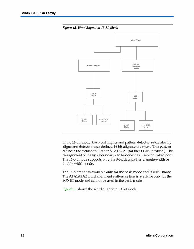
Figure 18. Word Aligner in 16-Bit Mode
In the 16-bit mode, the word aligner and pattern detector automatically aligns and detects a user-defined 16-bit alignment pattern. This pattern can be in the format of A1A2 or A1A1A2A2 (for the SONET protocol). The re-alignment of the byte boundary can be done via a user-controlled port. The 16-bit mode supports only the 8-bit data path in a single-width or double-width mode.
The 16-bit mode is available only for the basic mode and SONET mode. The A1A1A2A2 word alignment pattern option is available only for the SONET mode and cannot be used in the basic mode.
Figure 19 shows the word aligner in 10-bit mode.
Word Aligner
Pattern Detector
16-BitMode
A1A2Mode
A1A1A2A2Mode
ManualAlignment
Mode
16-BitMode
A1A2Mode
A1A1A2A2Mode
26 Altera CorporationPreliminary

Transceiver Blocks
Figure 19. Word Aligner in 10-Bit Mode
In the 10-bit mode, the word aligner automatically aligns the user’s predefined 10-bit alignment pattern. The pattern detector can detect the full 10-bit pattern or only the lower seven bits of the pattern. The word aligner and pattern detector detect both the positive and the negative disparity of the pattern. A user-controlled enable port is available for the word aligner.
The 10-bit mode is available only for the basic mode.
Figure 20 shows the word aligner in XAUI mode.
Word Aligner
Pattern Detector
10-BitMode
7-BitMode
ManualAlignment
Mode
10-BitMode
Altera Corporation 27Preliminary
Stratix GX FPGA Family
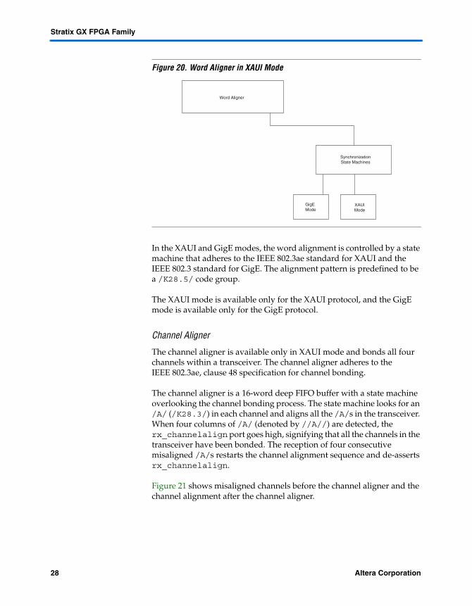
Figure 20. Word Aligner in XAUI Mode
In the XAUI and GigE modes, the word alignment is controlled by a state machine that adheres to the IEEE 802.3ae standard for XAUI and the IEEE 802.3 standard for GigE. The alignment pattern is predefined to be a /K28.5/ code group.
The XAUI mode is available only for the XAUI protocol, and the GigE mode is available only for the GigE protocol.
Channel Aligner
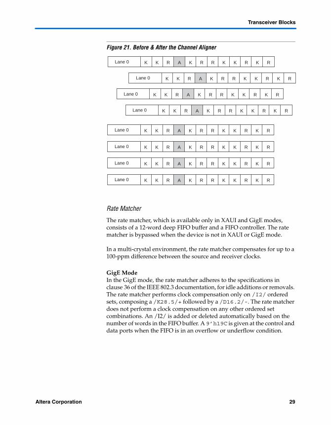
The channel aligner is available only in XAUI mode and bonds all four channels within a transceiver. The channel aligner adheres to the IEEE 802.3ae, clause 48 specification for channel bonding.
The channel aligner is a 16-word deep FIFO buffer with a state machine overlooking the channel bonding process. The state machine looks for an /A/ (/K28.3/) in each channel and aligns all the /A/s in the transceiver. When four columns of /A/ (denoted by //A//) are detected, the rx_channelalign port goes high, signifying that all the channels in the transceiver have been bonded. The reception of four consecutive misaligned /A/s restarts the channel alignment sequence and de-asserts rx_channelalign.
Figure 21 shows misaligned channels before the channel aligner and the channel alignment after the channel aligner.
Word Aligner
SynchronizationState Machines
XAUIMode
GigEMode
28 Altera CorporationPreliminary
Transceiver Blocks
Figure 21. Before & After the Channel Aligner
Rate Matcher
The rate matcher, which is available only in XAUI and GigE modes, consists of a 12-word deep FIFO buffer and a FIFO controller. The rate matcher is bypassed when the device is not in XAUI or GigE mode.
In a multi-crystal environment, the rate matcher compensates for up to a 100-ppm difference between the source and receiver clocks.
GigE ModeIn the GigE mode, the rate matcher adheres to the specifications in clause 36 of the IEEE 802.3 documentation, for idle additions or removals. The rate matcher performs clock compensation only on /I2/ ordered sets, composing a /K28.5/+ followed by a /D16.2/-. The rate matcher does not perform a clock compensation on any other ordered set combinations. An /I2/ is added or deleted automatically based on the number of words in the FIFO buffer. A 9’h19C is given at the control and data ports when the FIFO is in an overflow or underflow condition.
K RK K KRRR K KRALane 0
K RK K KRRR K KRALane 0
K RK K KRRR K KRALane 0
K RK K KRRR K KRALane 0
K RK K KRRR K KRALane 0
K RK K KRRR K KRALane 0
K RK K KRRR K KRALane 0
K RK K KRRR K KRALane 0
Altera Corporation 29Preliminary
Stratix GX FPGA Family
XAUI ModeIn XAUI mode, the rate matcher adheres to clause 48 of the IEEE 802.3ae specification for clock rate compensation. The rate matcher performs clock compensation on columns of /R/ (/K28.0/), denoted by //R//. An //R// is added or deleted automatically based on the number of words in the FIFO buffer.
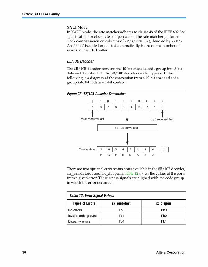
8B/10B Decoder
The 8B/10B decoder converts the 10-bit encoded code group into 8-bit data and 1 control bit. The 8B/10B decoder can be bypassed. The following is a diagram of the conversion from a 10-bit encoded code group into 8-bit data + 1-bit control.
Figure 22. 8B/10B Decoder Conversion
There are two optional error status ports available in the 8B/10B decoder, rx_errdetect and rx_disperr. Table 12 shows the values of the ports from a given error. These status signals are aligned with the code group in which the error occurred.
Table 12. Error Signal Values
Types of Errors rx_errdetect rx_disperr
No errors 1’b0 1’b0
Invalid code groups 1’b1 1’b0
Disparity errors 1’b1 1’b1
9 8 7 6 5 4 3 2 1 0
8b-10b conversion
j h g f i e d c b a
MSB received last LSB received first
7 6 5 4 3 2 1 0
H G F E D C B A
+ ctrlParallel data
30 Altera CorporationPreliminary
Transceiver Blocks
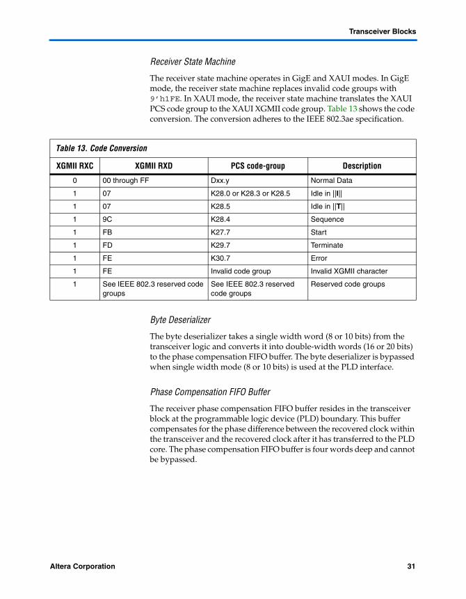
Receiver State Machine
The receiver state machine operates in GigE and XAUI modes. In GigE mode, the receiver state machine replaces invalid code groups with 9’h1FE. In XAUI mode, the receiver state machine translates the XAUI PCS code group to the XAUI XGMII code group. Table 13 shows the code conversion. The conversion adheres to the IEEE 802.3ae specification.
Byte Deserializer
The byte deserializer takes a single width word (8 or 10 bits) from the transceiver logic and converts it into double-width words (16 or 20 bits) to the phase compensation FIFO buffer. The byte deserializer is bypassed when single width mode (8 or 10 bits) is used at the PLD interface.
Phase Compensation FIFO Buffer
The receiver phase compensation FIFO buffer resides in the transceiver block at the programmable logic device (PLD) boundary. This buffer compensates for the phase difference between the recovered clock within the transceiver and the recovered clock after it has transferred to the PLD core. The phase compensation FIFO buffer is four words deep and cannot be bypassed.
Table 13. Code Conversion
XGMII RXC XGMII RXD PCS code-group Description
0 00 through FF Dxx.y Normal Data
1 07 K28.0 or K28.3 or K28.5 Idle in ||I||
1 07 K28.5 Idle in ||T||
1 9C K28.4 Sequence
1 FB K27.7 Start
1 FD K29.7 Terminate
1 FE K30.7 Error
1 FE Invalid code group Invalid XGMII character
1 See IEEE 802.3 reserved code groups
See IEEE 802.3 reserved code groups
Reserved code groups
Altera Corporation 31Preliminary

Stratix GX FPGA Family
Loopback Modes
The Stratix GX transceiver has built-in loopback modes to aid in debug and testing. The loopback modes are set in the Stratix GX MegaWizard Plug-In Manager in the Quartus II software. Only one loopback mode can be set at any single instance of the transceiver block. The loopback mode applies to all used channels in a transceiver block.
The available loopback modes are:
Serial loopback Parallel loopback Reverse serial loopback
Serial Loopback
Serial loopback exercises all the transceiver logic except for the output buffer and input buffer. The loopback function is dynamically switchable through the rx_slpbk port on a channel by channel basis. The VOD of the output is limited to 400 mV when the serial loopback option is selected. Figure 23 shows the data path in serial loopback mode.
Figure 23. Data Path in Serial Loopback Mode
Non-active Path
Active Path
ClockRecovery
Unit
BIST PRBSVerifier
BISTIncremental
VerifierChannelAligner Rate
Matcher 8B/10BDecoder Byte
Deserializer
PhaseCompensation
FIFO
ByteSerializerSerializer
BIST PRBSGenerator
8B/10BEncoder
Deserializer WordAligner
PhaseCompensation
FIFO
BISTGenerator
32 Altera CorporationPreliminary
Transceiver Blocks
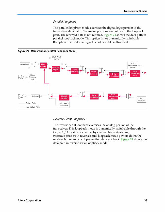
Parallel Loopback
The parallel loopback mode exercises the digital logic portion of the transceiver data path. The analog portions are not use in the loopback path. The received data is not retimed. Figure 24 shows the data path in parallel loopback mode. This option is not dynamically switchable. Reception of an external signal is not possible in this mode.
Figure 24. Data Path in Parallel Loopback Mode
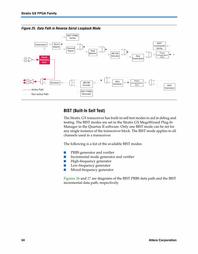
Reverse Serial Loopback
The reverse serial loopback exercises the analog portion of the transceiver. This loopback mode is dynamically switchable through the tx_srlpbk port on a channel by channel basis. Asserting rxanalogreset in reverse serial loopback mode powers down the receiver buffer and CRU, preventing data loopback. Figure 25 shows the data path in reverse serial loopback mode.
ClockRecovery
Unit
WordAligner
BIST PRBSVerifier
BISTIncremental
VerifierChannelAligner Rate
Matcher
BISTGenerator
ByteDeserializer
PhaseCompensation
FIFO
PhaseCompensation
FIFO
ByteSerializerSerializer
BIST PRBSGenerator
8B/10BEncoder
8B/10BDecoder
Deserializer
Non-active Path
Active Path
Altera Corporation 33Preliminary
Stratix GX FPGA Family
Figure 25. Data Path in Reverse Serial Loopback Mode
BIST (Built-In Self Test)
The Stratix GX transceiver has built-in self test modes to aid in debug and testing. The BIST modes are set in the Stratix GX MegaWizard Plug-In Manager in the Quartus II software. Only one BIST mode can be set for any single instance of the transceiver block. The BIST mode applies to all channels used in a transceiver.
The following is a list of the available BIST modes:
PRBS generator and verifier Incremental mode generator and verifier High-frequency generator Low-frequency generator Mixed-frequency generator
Figures 26 and 27 are diagrams of the BIST PRBS data path and the BIST incremental data path, respectively.
Non-active Path
Active Path
ClockRecovery
Unit
Deserializer
BIST PRBSVerifier
BISTIncremental
Verifier
BISTGenerator
ByteDeserializer
PhaseCompensation
FIFO
ByteSerializer
BIST PRBSGenerator
8B/10BEncoder
Serializer
PhaseCompensation
FIFO
8B/10BDecoder
RateMatcher
ChannelAligner
WordAligner
34 Altera CorporationPreliminary

Transceiver Blocks
Figure 26. BIST PRBS Data Path
Figure 27. BIST Incremental Data Path
Table 14 shows the BIST data output and verifier alignment pattern.
ClockRecovery
Unit
Deserializer WordAligner
BIST PRBSVerifier
BISTIncremental
Verifier
BISTGenerator
ByteDeserializer
PhaseCompensation
FIFO
PhaseCompensation
FIFO
ByteSerializer
ChannelAligner Rate
Matcher 8B/10BDecoder
Serializer
BIST PRBSGenerator
8B/10BEncoder
Non-active Path
Active Path
Deserializer WordAligner
BIST PRBSVerifier
ChannelAligner Rate
Matcher 8B/10BDecoder
BISTGenerator
ByteDeserializer
PhaseCompensation
FIFOSerializer
BIST PRBSGenerator
8B/10BEncoder
Non-active Path
Active Path
ClockRecovery
Unit
BISTIncremental
Verifier
PhaseCompensation
FIFO
ByteSerializer
Table 14. BIST Data Output & Verifier Alignment Pattern (Part 1 of 2)
BIST Mode Output Polynomials Verifier Word Alignment Pattern
PRBS 8-bit 28 – 1 x8 + x7 + x5 + x3 + 1 1000000011111111
PRBS 10-bit 210 – 1 x10 + x7 + 1 1111111111
Altera Corporation 35Preliminary
Stratix GX FPGA Family
Stratix GX Clocking
The Stratix GX global clock can be driven by certain REFCLKB pins, all transmitter PLL outputs, and all receiver PLL outputs. The REFCLKB pins (except for transceiver block 0 and transceiver block 4) can drive inter-transceiver and global clock lines as well as feed the transmitter and receiver PLLs. The output of the transmitter PLL can only feed global clock lines and the reference clock port of the receiver PLL.
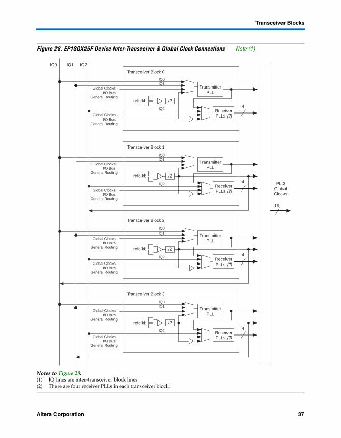
Figures 28 and 29 are diagrams of the Inter-Transceiver line connections as well as the global clock connections for the EP1SGX25F and EP1SGX40G devices. For devices with fewer transceivers, ignore the information about the unavailable transceiver blocks.
PRBS 16-bit 28 – 1 x8 + x7 + x5 + x3 + 1 1000000011111111
PRBS 20-bit 210 – 1 x10 + x7 + 1 1111111111
Incremental 10-bit K28.5, K27.7, Data (00-FF incremental), K28.0, K28.1, K28.2, K28.3, K28.4, K28.6, K28.7, K23.7, K30.7, K29.7 (1)
0101111100 (K28.5)
Incremental 20-bit K28.5, K27.7, Data (00-FF incremental), K28.0, K28.1, K28.2, K28.3, K28.4, K28.6, K28.7, K23.7, K30.7, K29.7 (1)
0101111100 (K28.5)
High frequency 1010101010
Low frequency 0011111000
Mixed frequency 0011111010 or 1100000101
Note to Table 14:(1) This output repeats.
Table 14. BIST Data Output & Verifier Alignment Pattern (Part 2 of 2)
BIST Mode Output Polynomials Verifier Word Alignment Pattern
36 Altera CorporationPreliminary
Transceiver Blocks
Figure 28. EP1SGX25F Device Inter-Transceiver & Global Clock Connections Note (1)
Notes to Figure 28:(1) IQ lines are inter-transceiver block lines.(2) There are four receiver PLLs in each transceiver block.
IQ0 IQ1 IQ2
PLDGlobalClocks
16
Global Clocks, I/O Bus,
General Routing
ReceiverPLLs (2)
IQ0IQ1
Global Clocks, I/O Bus,
General Routing
IQ2
Transceiver Block 0
/24
refclkb
refclkb
refclkb
refclkb
TransmitterPLL
Global Clocks, I/O Bus,
General Routing
ReceiverPLLs (2)
IQ0IQ1
Global Clocks, I/O Bus,
General Routing
IQ2
Transceiver Block 1
/24
TransmitterPLL
Global Clocks, I/O Bus,
General Routing
ReceiverPLLs (2)
IQ0IQ1
Global Clocks, I/O Bus,
General Routing
IQ2
Transceiver Block 2
/24
TransmitterPLL
Global Clocks, I/O Bus,
General Routing
ReceiverPLLs (2)
IQ0IQ1
Global Clocks, I/O Bus,
General Routing
IQ2
Transceiver Block 3
/24
TransmitterPLL
Altera Corporation 37Preliminary

Stratix GX FPGA Family
Figure 29. EP1SGX40G Device Inter-Transceiver & Global Clock Connections Note (1)
Notes to Figure 29:(1) IQ lines are inter-transceiver block lines.(2) There are four receiver PLLs in each transceiver block.
IQ0 IQ1 IQ2
PLDGlobalClocks
16
Global Clocks, I/O Bus,
General Routing
ReceiverPLLs (2)
IQ0IQ1
Global Clocks, I/O Bus,
General Routing
IQ2
Transceiver Block 0
/24
TransmitterPLL
Global Clocks, I/O Bus,
General Routing
ReceiverPLLs (2)
IQ0IQ1
Global Clocks, I/O Bus,
General Routing
IQ2
Transceiver Block 1
/24
TransmitterPLL
Global Clocks, I/O Bus,
General Routing
ReceiverPLLs (2)
IQ0IQ1
Global Clocks, I/O Bus,
General Routing
IQ2
Transceiver Block 4
/24
TransmitterPLL
Global Clocks, I/O Bus,
General Routing
ReceiverPLLs (2)
IQ0IQ1
Global Clocks, I/O Bus,
General Routing
IQ2
Transceiver Block 2
/24
TransmitterPLL
Global Clocks, I/O Bus,
General Routing
ReceiverPLLs (2)
IQ0IQ1
Global Clocks, I/O Bus,
General Routing
IQ2
Transceiver Block 3
/24
TransmitterPLL
refclkb
refclkb
refclkb
refclkb
refclkb
38 Altera CorporationPreliminary

Transceiver Blocks
The receiver PLL can also drive the fast regional, regional clocks, and local routing adjacent to the associated transceiver block. Figures 30 through 33 show which fast regional and regional clock resource can be used by the recovered clock.
In the EP1SGX25 device, the receiver PLL recovered clocks from transceiver blocks 0 and 1 drive RCLK[1..0] while transceiver blocks 2 and 3 drive RCLK[7..6]. The regional clocks feed logic in their associated regions.
Figure 30. EP1SGX25 Receiver PLL Recovered Clock to Regional Clock Connection
In addition, the receiver PLL’s recovered clocks can drive fast regional lines (FCLK) as shown Figure 31. The fast regional clocks can feed logic in their associated regions.
Stratix GXTransceiver BlocksPLD
RCLK[11..10]
Block 0
Block 1
Block 2
Block 3
RCLK[9..8]
Altera Corporation 39Preliminary
Stratix GX FPGA Family
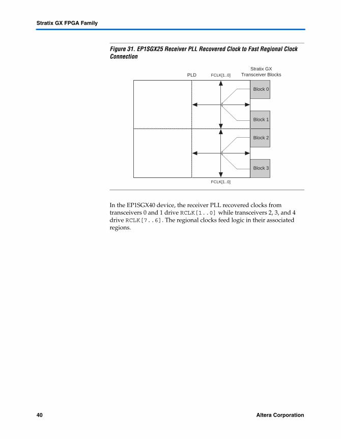
Figure 31. EP1SGX25 Receiver PLL Recovered Clock to Fast Regional Clock Connection
In the EP1SGX40 device, the receiver PLL recovered clocks from transceivers 0 and 1 drive RCLK[1..0] while transceivers 2, 3, and 4 drive RCLK[7..6]. The regional clocks feed logic in their associated regions.
PLD FCLK[1..0]
FCLK[1..0]
Block 0
Block 1
Block 2
Block 3
Stratix GXTransceiver Blocks
40 Altera CorporationPreliminary

Transceiver Blocks
Figure 32. EP1SGX40 Receiver PLL Recovered Clock to Regional Clock Connection
Figure 33 shows the possible recovered clock connection to the fast regional clock resource. The fast regional clocks can drive logic in their associated regions.
PLDStratix GX
Transceiver Blocks
Block 0
Block 1
Block 4
Block 2
Block 3
RCLK[9..8]
RCLK[11..10]
Altera Corporation 41Preliminary

Stratix GX FPGA Family
Figure 33. EP1SGX40 Receiver PLL Recovered Clock to Fast Regional Clock Connection
Table 15 summarizes the possible clocking connections for the transceivers.
PLD FCLK[1..0]
FCLK[1..0]
Stratix GXTransceiver Blocks
Block 0
Block 1
Block 4
Block 2
Block 3
Table 15. Possible Clocking Connections for Transceivers (Part 1 of 2)
Source
Destination
Transmitter PLL
Receiver PLL GCLK RCLK FCLK IQ Lines
REFCLKB v v v (1) v v (1)
Transmitter PLL v v v v
Receiver PLL v v v
GCLK v v
RCLK v v
FCLK v v
42 Altera CorporationPreliminary

Other Transceiver Features
Other Transceiver Features
Other important features of the Stratix GX transceivers are the power down and reset capabilities, the external voltage reference and bias circuitry, and hot swapping.
Individual Power-Down & Reset for the Transmitter & Receiver
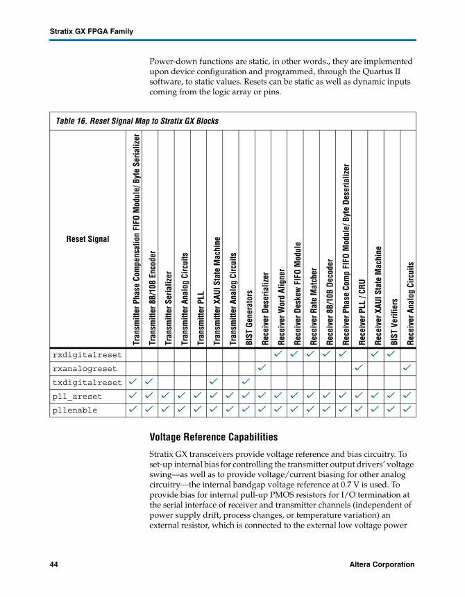
Stratix GX transceivers offer a power saving advantage with their ability to shut off functions that are not needed. The device can individually reset the receiver and transmitter blocks and the PLLs. The Stratix GX device can either globally power down and reset the transmitter and receiver channels or do each channel separately. Table 16 shows the connectivity between the reset signals and the Stratix GX logical blocks.
IQ lines v (2) v (2)
Notes to Table 15:(1) REFCLKB from transceiver block 0 and transceiver block 4 does not drive the inter-transceiver lines or the GCLK
lines.(2) Inter-transceiver line 0 and inter-transceiver line 1 drive the transmitter PLL, while inter-transceiver line 2 drives
the receiver PLLs.
Table 15. Possible Clocking Connections for Transceivers (Part 2 of 2)
Source
Destination
Transmitter PLL
Receiver PLL GCLK RCLK FCLK IQ Lines
Altera Corporation 43Preliminary
Stratix GX FPGA Family
Power-down functions are static, in other words., they are implemented upon device configuration and programmed, through the Quartus II software, to static values. Resets can be static as well as dynamic inputs coming from the logic array or pins.
Voltage Reference Capabilities
Stratix GX transceivers provide voltage reference and bias circuitry. To set-up internal bias for controlling the transmitter output drivers’ voltage swing—as well as to provide voltage/current biasing for other analog circuitry—the internal bandgap voltage reference at 0.7 V is used. To provide bias for internal pull-up PMOS resistors for I/O termination at the serial interface of receiver and transmitter channels (independent of power supply drift, process changes, or temperature variation) an external resistor, which is connected to the external low voltage power
Table 16. Reset Signal Map to Stratix GX Blocks
Reset Signal
Tran
smitt
er P
hase
Com
pens
atio
n FI
FO M
odul
e/ B
yte
Seria
lizer
Tran
smitt
er 8
B/10
B En
code
r
Tran
smitt
er S
eria
lizer
Tran
smitt
er A
nalo
g Ci
rcui
ts
Tran
smitt
er P
LL
Tran
smitt
er X
AUI S
tate
Mac
hine
Tran
smitt
er A
nalo
g Ci
rcui
ts
BIST
Gen
erat
ors
Rece
iver
Des
eria
lizer
Rece
iver
Wor
d Al
igne
r
Rece
iver
Des
kew
FIF
O M
odul
e
Rece
iver
Rat
e M
atch
er
Rece
iver
8B/
10B
Deco
der
Rece
iver
Pha
se C
omp
FIFO
Mod
ule/
Byt
e De
seria
lizer
Rece
iver
PLL
/ CR
U
Rece
iver
XAU
I Sta
te M
achi
ne
BIST
Ver
ifier
s
Rece
iver
Ana
log
Circ
uits
rxdigitalreset v v v v v v v
rxanalogreset v v v
txdigitalreset v v v v
pll_areset v v v v v v v v v v v v v v v v v v
pllenable v v v v v v v v v v v v v v v v v v
44 Altera CorporationPreliminary
Applications & Protocols Supported with Stratix GX Devices
supply, is accurately tracked by the internal bias circuit. Moreover, the reference voltage and internal resistor bias current is generated and replicated to the analog circuitry in each channel.
Hot-Socketing Capabilities
Each Stratix GX device is capable of hot-socketing. Because Stratix GX devices can be used in a mixed-voltage environment, they have been designed specifically to tolerate any possible power-up sequence. Signals can be driven into Stratix GX devices before and during power-up without damaging the device. Once operating conditions are reached and the device is configured, Stratix GX devices operate as specified by the designer. This feature provides the Stratix GX transceiver line card behavior, so designers can insert it into the system without powering the system down, offering more flexibility.
Applications & Protocols Supported with Stratix GX Devices
Each Stratix GX transceiver block is designed to operate at any serial bit rate from 500 Mbps to 3.1875 Gbps per channel. The wide, data rate range allows Stratix GX transceivers to support a wide variety of standard and future protocols such as 10-Gigabit Ethernet XAUI, InfiniBand, Fibre Channel, and Serial RapidIO. Stratix GX devices are ideal for many high-speed communication applications such as high-speed backplanes, chip-to-chip bridges, and high-speed serial communications standards support.
Stratix GX Example Application Support
Stratix GX devices can be used for many applications, including:
Backplanes for traffic management and quality of service (QOS) Switch fabric applications for complete set for backplane and switch
fabric transceivers Chip-to-chip applications such as: 10 Gigabit Ethernet XAUI to
XGMII bridge, 10 Gigabit Ethernet XGMII to POS-PHY4 bridge, POS-PHY4 to NPSI bridge, or NPSI to backplane bridge
Altera Corporation 45Preliminary
Stratix GX FPGA Family
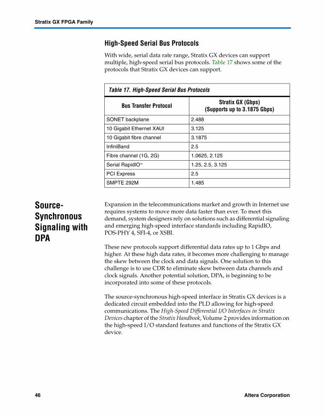
High-Speed Serial Bus Protocols
With wide, serial data rate range, Stratix GX devices can support multiple, high-speed serial bus protocols. Table 17 shows some of the protocols that Stratix GX devices can support.
Source-Synchronous Signaling with DPA
Expansion in the telecommunications market and growth in Internet use requires systems to move more data faster than ever. To meet this demand, system designers rely on solutions such as differential signaling and emerging high-speed interface standards including RapidIO, POS-PHY 4, SFI-4, or XSBI.
These new protocols support differential data rates up to 1 Gbps and higher. At these high data rates, it becomes more challenging to manage the skew between the clock and data signals. One solution to this challenge is to use CDR to eliminate skew between data channels and clock signals. Another potential solution, DPA, is beginning to be incorporated into some of these protocols.
The source-synchronous high-speed interface in Stratix GX devices is a dedicated circuit embedded into the PLD allowing for high-speed communications. The High-Speed Differential I/O Interfaces in Stratix Devices chapter of the Stratix Handbook, Volume 2 provides information on the high-speed I/O standard features and functions of the Stratix GX device.
Table 17. High-Speed Serial Bus Protocols
Bus Transfer Protocol Stratix GX (Gbps)(Supports up to 3.1875 Gbps)
SONET backplane 2.488
10 Gigabit Ethernet XAUI 3.125
10 Gigabit fibre channel 3.1875
InfiniBand 2.5
Fibre channel (1G, 2G) 1.0625, 2.125
Serial RapidIO™ 1.25, 2.5, 3.125
PCI Express 2.5
SMPTE 292M 1.485
46 Altera CorporationPreliminary
Source-Synchronous Signaling with DPA
Stratix GX I/O Banks
Stratix GX devices contain 17 I/O banks, as shown in Figure 1 on page 5. I/O banks one and two support high-speed LVDS, LVPECL, and 3.3-V PCML inputs and outputs. These two banks also incorporate an embedded dynamic phase aligner within the source-synchronous interface (see Figure 41 on page 56). The dynamic phase aligner corrects for the phase difference between the clock and data lines caused by skew. The dynamic phase aligner operates automatically and continuously without requiring a fixed training pattern, and allows the source-synchronous circuitry to capture data correctly regardless of the channel-to-clock skew.
Principles of SERDES Operation
Stratix GX devices support source-synchronous differential signaling up to 1 Gbps in DPA mode, and up to 840 Mbps in non-DPA mode. Serial data is transmitted and received along with a low-frequency clock. The PLL can multiply the incoming low-frequency clock by a factor of 1 to 10. The SERDES factor J can be 8 or 10 for the DPA mode, or 4, 7, 8, or 10 for all other modes. The SERDES factor does not have to equal the clock multiplication value. The ×1 and ×2 operation is also possible by bypassing the SERDES. The SERDES DPA cannot support ×1, ×2, or ×4 natively.
On the receiver side, the high-frequency clock generated by the PLL shifts the serial data through a shift register (also called deserializer). The parallel data is clocked out to the logic array synchronized with the low-frequency clock. On the transmitter side, the parallel data from the logic array is first clocked into a parallel-in, serial-out shift register synchronized with the low-frequency clock and then transmitted out by the output buffers.
There are two dedicated fast PLLs each in EP1SGX10 to EP1SGX25 devices, and four in EP1SGX40 devices. These PLLs are used for the SERDES operations as well as general-purpose use.
Stratix GX Differential I/O Receiver Operation (Non-DPA Mode)
Designers can configure any of the Stratix GX source synchronous differential input channels as a receiver channel (see Figure 34). The differential receiver deserializes the incoming high-speed data. The input shift register continuously clocks the incoming data on the negative transition of the high-frequency clock generated by the PLL clock (×W).
Altera Corporation 47Preliminary

Stratix GX FPGA Family
The data in the serial shift register is shifted into a parallel register by the RXLOADEN signal generated by the fast PLL counter circuitry on the third falling edge of the high-frequency clock. However, designers can select which falling edge of the high frequency clock loads the data into the parallel register, using the data-realignment circuit.
In normal mode, the enable signal RXLOADEN loads the parallel data into the next parallel register on the second rising edge of the low-frequency clock. Designers can also load data to the parallel register through the TXLOADEN signal when using the data-realignment circuit.
Figure 34 shows the block diagram of a single SERDES receiver channel. Figure 35 shows the timing relationship between the data and clocks in Stratix GX devices in ×10 mode. W is the low-frequency multiplier and J is the data parallelization division factor.
Figure 34. Stratix GX High-Speed Interface Deserialized in ×10 Mode
Notes to Figure 34:(1) W = 1, 2, 4, 7, 8, or 10.
J = 4, 7, 8, or 10 for non-DPA (J = 8 or 10 for DPA).W does not have to equal J. When J = 1 or 2, the deserializer is bypassed. When J = 2, the device uses DDRIO registers.
(2) This figure does not show additional circuitry for clock or data manipulation.
PD0PD1PD2PD3PD4PD5PD6PD7PD8PD9
PD0PD1PD2PD3PD4PD5PD6PD7PD8PD9
PD0PD1PD2PD3PD4PD5PD6PD7PD8PD9
Stratix GXLogic Array
Receiver Circuit
Serial ShiftRegisters
ParallelRegisters
ParallelRegisters
FastPLL (2)
RXIN+
RXIN−
RXCLKIN+
RXCLKIN−
×W ×W/J (1)
RXLOADEN
TXLOADEN
48 Altera CorporationPreliminary

Source-Synchronous Signaling with DPA
Figure 35. Receiver Timing Diagram
Stratix GX Differential I/O Transmitter Operation
Designers can configure any of the Stratix GX differential output channels as a transmitter channel. The differential transmitter is used to serialize outbound parallel data.
The logic array sends parallel data to the SERDES transmitter circuit when the TXLOADEN signal is asserted. This signal is generated by the high-speed counter circuitry of the logic array low-frequency clock’s rising edge. The data is then transferred from the parallel register into the serial shift register by the TXLOADEN signal on the third rising edge of the high-frequency clock.
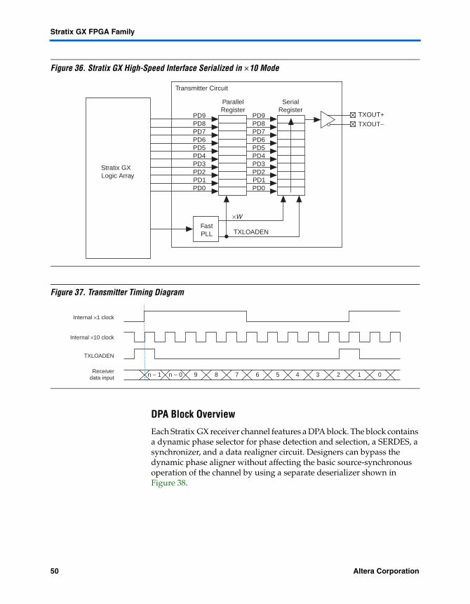
Figure 36 shows the block diagram of a single SERDES transmitter channel and Figure 37 shows the timing relationship between the data and clocks in Stratix GX devices in ×10 mode. W is the low-frequency multiplier and J is the data parallelization division factor.
RXLOADEN
Internal ×1 clock
Internal ×10 clock
Receiverdata input n – 1 n – 0 9 8 7 6 5 4 3 2 1 0
Altera Corporation 49Preliminary
Stratix GX FPGA Family
Figure 36. Stratix GX High-Speed Interface Serialized in ×10 Mode
Figure 37. Transmitter Timing Diagram
DPA Block Overview
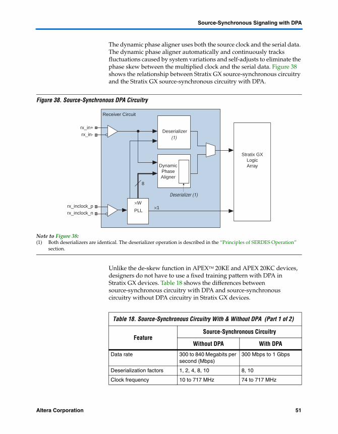
Each Stratix GX receiver channel features a DPA block. The block contains a dynamic phase selector for phase detection and selection, a SERDES, a synchronizer, and a data realigner circuit. Designers can bypass the dynamic phase aligner without affecting the basic source-synchronous operation of the channel by using a separate deserializer shown in Figure 38.
PD9PD8PD7PD6PD5PD4PD3PD2PD1PD0
PD9PD8PD7PD6PD5PD4PD3PD2PD1PD0
Stratix GX Logic Array
Transmitter Circuit
ParallelRegister
SerialRegister
FastPLL
TXOUT+
TXOUT−
×W
TXLOADEN
TXLOADEN
Internal ×1 clock
Internal ×10 clock
Receiverdata input n – 1 n – 0 9 8 7 6 5 4 3 2 1 0
50 Altera CorporationPreliminary
Source-Synchronous Signaling with DPA
The dynamic phase aligner uses both the source clock and the serial data. The dynamic phase aligner automatically and continuously tracks fluctuations caused by system variations and self-adjusts to eliminate the phase skew between the multiplied clock and the serial data. Figure 38 shows the relationship between Stratix GX source-synchronous circuitry and the Stratix GX source-synchronous circuitry with DPA.
Figure 38. Source-Synchronous DPA Circuitry
Note to Figure 38:(1) Both deserializers are identical. The deserializer operation is described in the “Principles of SERDES Operation”
section.
Unlike the de-skew function in APEXTM 20KE and APEX 20KC devices, designers do not have to use a fixed training pattern with DPA in Stratix GX devices. Table 18 shows the differences between source-synchronous circuitry with DPA and source-synchronous circuitry without DPA circuitry in Stratix GX devices.
PLL
DynamicPhaseAligner
Deserializer
Stratix GXLogicArray
Receiver Circuit
×W×1
rx_in+
rx_in-
rx_inclock_p
rx_inclock_n
8
Deserializer (1)
(1)
Table 18. Source-Synchronous Circuitry With & Without DPA (Part 1 of 2)
FeatureSource-Synchronous Circuitry
Without DPA With DPA
Data rate 300 to 840 Megabits per second (Mbps)
300 Mbps to 1 Gbps
Deserialization factors 1, 2, 4, 8, 10 8, 10
Clock frequency 10 to 717 MHz 74 to 717 MHz
Altera Corporation 51Preliminary
Stratix GX FPGA Family
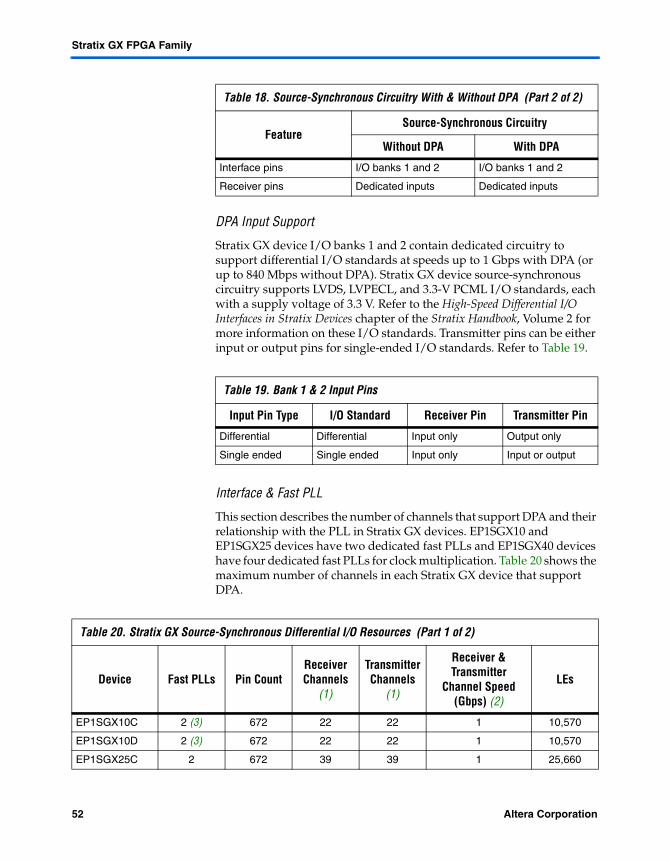
DPA Input Support
Stratix GX device I/O banks 1 and 2 contain dedicated circuitry to support differential I/O standards at speeds up to 1 Gbps with DPA (or up to 840 Mbps without DPA). Stratix GX device source-synchronous circuitry supports LVDS, LVPECL, and 3.3-V PCML I/O standards, each with a supply voltage of 3.3 V. Refer to the High-Speed Differential I/O Interfaces in Stratix Devices chapter of the Stratix Handbook, Volume 2 for more information on these I/O standards. Transmitter pins can be either input or output pins for single-ended I/O standards. Refer to Table 19.
Interface & Fast PLL
This section describes the number of channels that support DPA and their relationship with the PLL in Stratix GX devices. EP1SGX10 and EP1SGX25 devices have two dedicated fast PLLs and EP1SGX40 devices have four dedicated fast PLLs for clock multiplication. Table 20 shows the maximum number of channels in each Stratix GX device that support DPA.
Interface pins I/O banks 1 and 2 I/O banks 1 and 2
Receiver pins Dedicated inputs Dedicated inputs
Table 19. Bank 1 & 2 Input Pins
Input Pin Type I/O Standard Receiver Pin Transmitter Pin
Differential Differential Input only Output only
Single ended Single ended Input only Input or output
Table 18. Source-Synchronous Circuitry With & Without DPA (Part 2 of 2)
FeatureSource-Synchronous Circuitry
Without DPA With DPA
Table 20. Stratix GX Source-Synchronous Differential I/O Resources (Part 1 of 2)
Device Fast PLLs Pin CountReceiver Channels
(1)
Transmitter Channels
(1)
Receiver & Transmitter
Channel Speed (Gbps) (2)
LEs
EP1SGX10C 2 (3) 672 22 22 1 10,570
EP1SGX10D 2 (3) 672 22 22 1 10,570
EP1SGX25C 2 672 39 39 1 25,660
52 Altera CorporationPreliminary
Source-Synchronous Signaling with DPA
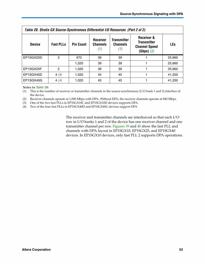
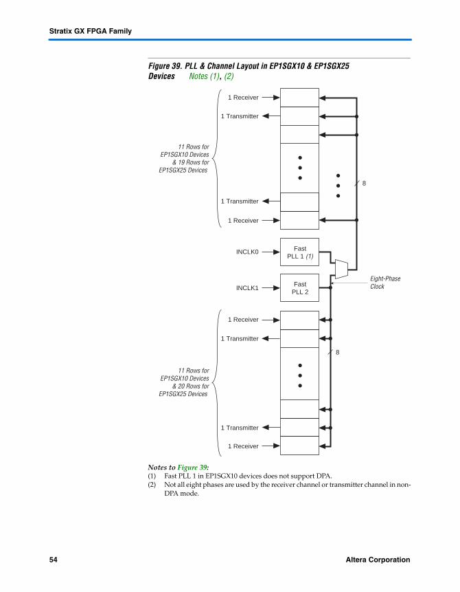
The receiver and transmitter channels are interleaved so that each I/O row in I/O banks 1 and 2 of the device has one receiver channel and one transmitter channel per row. Figures 39 and 40 show the fast PLL and channels with DPA layout in EP1SGX10, EP1SGX25, and EP1SGX40 devices. In EP1SGX10 devices, only fast PLL 2 supports DPA operations.
EP1SGX25D 2 672 39 39 1 25,660
1,020 39 39 1 25,660
EP1SGX25F 2 1,020 39 39 1 25,660
EP1SGX40D 4 (4) 1,020 45 45 1 41,250
EP1SGX40G 4 (4) 1,020 45 45 1 41,250
Notes to Table 20:(1) This is the number of receiver or transmitter channels in the source-synchronous (I/O bank 1 and 2) interface of
the device.(2) Receiver channels operate at 1,000 Mbps with DPA. Without DPA, the receiver channels operate at 840 Mbps.(3) One of the two fast PLLs in EP1SGX10C and EP1SGX10D devices supports DPA.(4) Two of the four fast PLLs in EP1SGX40D and EP1SGX40G devices support DPA
Table 20. Stratix GX Source-Synchronous Differential I/O Resources (Part 2 of 2)
Device Fast PLLs Pin CountReceiver Channels
(1)
Transmitter Channels
(1)
Receiver & Transmitter
Channel Speed (Gbps) (2)
LEs
Altera Corporation 53Preliminary
Stratix GX FPGA Family
Figure 39. PLL & Channel Layout in EP1SGX10 & EP1SGX25 Devices Notes (1), (2)
Notes to Figure 39:(1) Fast PLL 1 in EP1SGX10 devices does not support DPA.(2) Not all eight phases are used by the receiver channel or transmitter channel in non-
DPA mode.
FastPLL 1 (1)
FastPLL 2
1 Receiver
1 Receiver
1 Transmitter
1 Transmitter
1 Receiver
1 Receiver
1 Transmitter
1 Transmitter
INCLK0
INCLK1
11 Rows forEP1SGX10 Devices
& 20 Rows forEP1SGX25 Devices
11 Rows forEP1SGX10 Devices
& 19 Rows forEP1SGX25 Devices
8
Eight-PhaseClock
8
54 Altera CorporationPreliminary
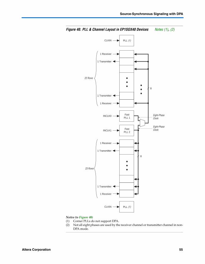
Source-Synchronous Signaling with DPA
Figure 40. PLL & Channel Layout in EP1SGX40 Devices Notes (1), (2)
Notes to Figure 40:(1) Corner PLLs do not support DPA.(2) Not all eight phases are used by the receiver channel or transmitter channel in non-
DPA mode.
FastPLL 1
FastPLL 2
1 Receiver
1 Receiver
1 Transmitter
1 Transmitter
1 Receiver
1 Receiver
1 Transmitter
1 Transmitter
INCLK0
PLL (1)CLKIN
PLL (1)CLKIN
INCLK1
23 Rows
22 Rows
8
Eight-PhaseClock
Eight-PhaseClock
8
Altera Corporation 55Preliminary
Stratix GX FPGA Family
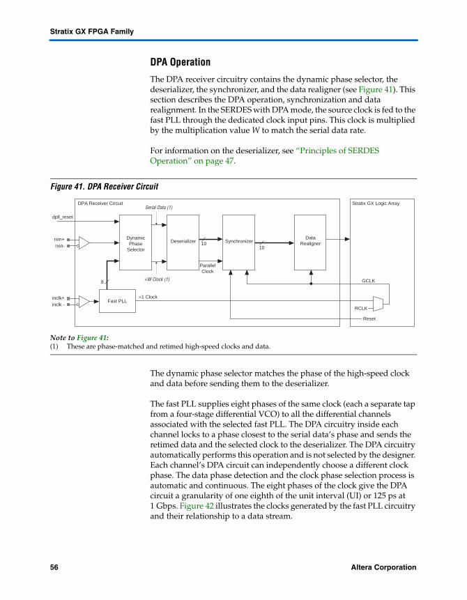
DPA Operation
The DPA receiver circuitry contains the dynamic phase selector, the deserializer, the synchronizer, and the data realigner (see Figure 41). This section describes the DPA operation, synchronization and data realignment. In the SERDES with DPA mode, the source clock is fed to the fast PLL through the dedicated clock input pins. This clock is multiplied by the multiplication value W to match the serial data rate.
For information on the deserializer, see “Principles of SERDES Operation” on page 47.
Figure 41. DPA Receiver Circuit
Note to Figure 41:(1) These are phase-matched and retimed high-speed clocks and data.
The dynamic phase selector matches the phase of the high-speed clock and data before sending them to the deserializer.
The fast PLL supplies eight phases of the same clock (each a separate tap from a four-stage differential VCO) to all the differential channels associated with the selected fast PLL. The DPA circuitry inside each channel locks to a phase closest to the serial data’s phase and sends the retimed data and the selected clock to the deserializer. The DPA circuitry automatically performs this operation and is not selected by the designer. Each channel’s DPA circuit can independently choose a different clock phase. The data phase detection and the clock phase selection process is automatic and continuous. The eight phases of the clock give the DPA circuit a granularity of one eighth of the unit interval (UI) or 125 ps at 1 Gbps. Figure 42 illustrates the clocks generated by the fast PLL circuitry and their relationship to a data stream.
rxin+rxin-
inclk+inclk -
Fast PLL
DynamicPhase
Selector
Deserializer
ParallelClock
SynchronizerData
Realigner
×W Clock (1)
×1 Clock
Serial Data (1)Stratix GX Logic ArrayDPA Receiver Circuit
GCLK
RCLK
Reset
8
1010
dpll_reset
56 Altera CorporationPreliminary

Source-Synchronous Signaling with DPA
Figure 42. Fast PLL Clocks & Data Input
Protocols, Training Pattern & DPA Lock Time
The dynamic phase aligner uses a fast PLL for clock multiplication, and the dynamic phase selector for the phase detection and alignment. The dynamic phase aligner uses the high-speed clock out of the dynamic phase selector to deserialize high-speed data and the receiver's source synchronous operations.
At each rising edge of the clock, the dynamic phase selector determines the phase difference between the clock and the data and automatically compensates for the phase difference between the data and clock.
Clock A
Data input
Clock B
Clock C
Clock D
Clock C'
Clock D'
Clock A'
Clock B'
D0 D1 D2 D3 D4 D5 Dn
Altera Corporation 57Preliminary
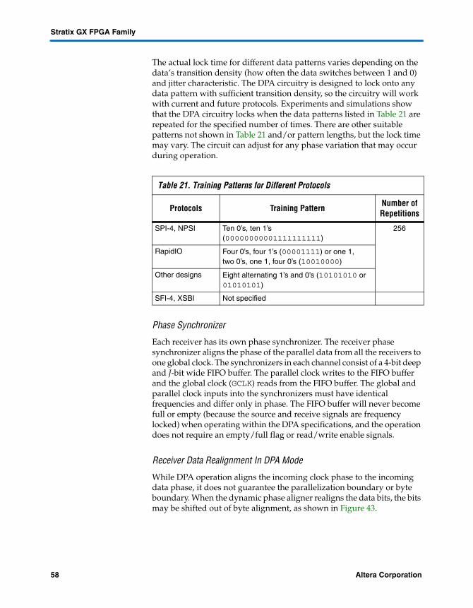
Stratix GX FPGA Family
The actual lock time for different data patterns varies depending on the data’s transition density (how often the data switches between 1 and 0) and jitter characteristic. The DPA circuitry is designed to lock onto any data pattern with sufficient transition density, so the circuitry will work with current and future protocols. Experiments and simulations show that the DPA circuitry locks when the data patterns listed in Table 21 are repeated for the specified number of times. There are other suitable patterns not shown in Table 21 and/or pattern lengths, but the lock time may vary. The circuit can adjust for any phase variation that may occur during operation.
Phase Synchronizer
Each receiver has its own phase synchronizer. The receiver phase synchronizer aligns the phase of the parallel data from all the receivers to one global clock. The synchronizers in each channel consist of a 4-bit deep and J-bit wide FIFO buffer. The parallel clock writes to the FIFO buffer and the global clock (GCLK) reads from the FIFO buffer. The global and parallel clock inputs into the synchronizers must have identical frequencies and differ only in phase. The FIFO buffer will never become full or empty (because the source and receive signals are frequency locked) when operating within the DPA specifications, and the operation does not require an empty/full flag or read/write enable signals.
Receiver Data Realignment In DPA Mode
While DPA operation aligns the incoming clock phase to the incoming data phase, it does not guarantee the parallelization boundary or byte boundary. When the dynamic phase aligner realigns the data bits, the bits may be shifted out of byte alignment, as shown in Figure 43.
Table 21. Training Patterns for Different Protocols
Protocols Training Pattern Number of Repetitions
SPI-4, NPSI Ten 0’s, ten 1’s (00000000001111111111)
256
RapidIO Four 0’s, four 1’s (00001111) or one 1, two 0’s, one 1, four 0’s (10010000)
Other designs Eight alternating 1’s and 0’s (10101010 or 01010101)
SFI-4, XSBI Not specified
58 Altera CorporationPreliminary
Source-Synchronous Signaling with DPA
Figure 43. Misaligned Captured Bits
The dynamic phase selector and synchronizer align the clock and data based on the power-up of both communicating devices, and the channel to channel skew. However, the dynamic phase selector and synchronizer cannot determine the byte boundary, and the data may need to be byte-aligned. The dynamic phase aligner’s data realignment circuitry shifts data bits to correct bit misalignments.
The Stratix GX circuitry contains a data-realignment feature controlled by the logic array. Stratix GX devices perform data realignment on the parallel data after the deserialization block. The data realignment can be performed per channel for more flexibility. The data alignment operation requires a state machine to recognize a specific pattern. The procedure requires the bits to be slipped on the data stream to correctly align the incoming data to the start of the byte boundary.
The DPA uses its realignment circuitry and the global clock for data realignment. Either a device pin or the logic array asserts the internal rx_channel_data_align node to activate the DPA data-realignment circuitry. Switching this node from low to high activates the realignment circuitry and the data being transferred to the logic array is shifted by one bit. The data realignment block cannot be bypassed. However, if the rx_channel_data_align is not turned on (through the altvlds MegaWizard Plug-In Manager), or when it is not toggled, it will only act as a register latency.
A state machine and additional logic can monitor the incoming parallel data and compare it against a known pattern. If the incoming data pattern does not match the known pattern, designers can activate the rx_channel_data_align node again. Repeat this process until the realigner detects the desired match between the known data pattern and incoming parallel data pattern.
0 1 2 3 4 5 6 7
3 4 5 6 7 0 1 2
Correct Alignment
Incorrect Alignment
Altera Corporation 59Preliminary
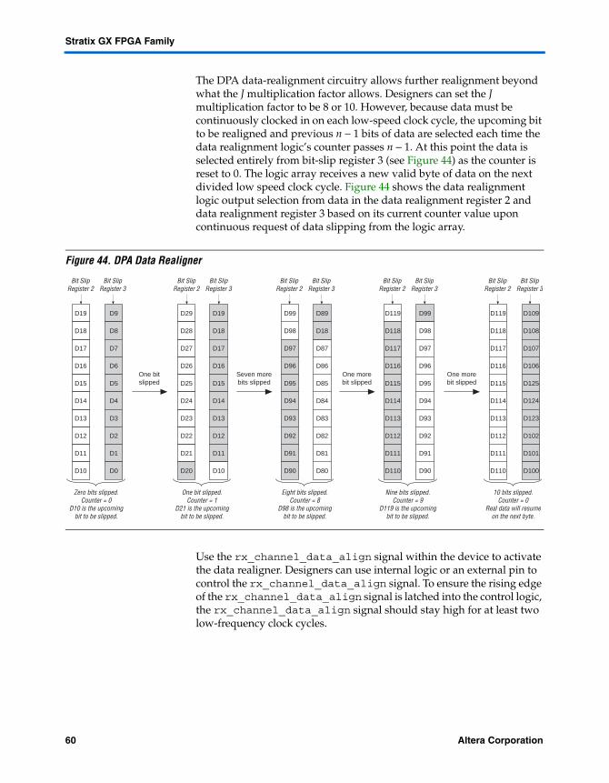
Stratix GX FPGA Family
The DPA data-realignment circuitry allows further realignment beyond what the J multiplication factor allows. Designers can set the J multiplication factor to be 8 or 10. However, because data must be continuously clocked in on each low-speed clock cycle, the upcoming bit to be realigned and previous n − 1 bits of data are selected each time the data realignment logic’s counter passes n − 1. At this point the data is selected entirely from bit-slip register 3 (see Figure 44) as the counter is reset to 0. The logic array receives a new valid byte of data on the next divided low speed clock cycle. Figure 44 shows the data realignment logic output selection from data in the data realignment register 2 and data realignment register 3 based on its current counter value upon continuous request of data slipping from the logic array.
Figure 44. DPA Data Realigner
Use the rx_channel_data_align signal within the device to activate the data realigner. Designers can use internal logic or an external pin to control the rx_channel_data_align signal. To ensure the rising edge of the rx_channel_data_align signal is latched into the control logic, the rx_channel_data_align signal should stay high for at least two low-frequency clock cycles.
D19
D18
D17
D16
D15
D14
D13
D12
D11
D10
D9
D8
D7
D6
D5
D4
D3
D2
D1
D0
One bitslipped
Zero bits slipped.Counter = 0
D10 is the upcomingbit to be slipped.
Bit SlipRegister 2
Bit SlipRegister 3
D29
D28
D27
D26
D25
D24
D23
D22
D21
D20
D19
D18
D17
D16
D15
D14
D13
D12
D11
D10
Seven morebits slipped
One bit slipped.Counter = 1
D21 is the upcomingbit to be slipped.
Bit SlipRegister 2
Bit SlipRegister 3
D99
D98
D97
D96
D95
D94
D93
D92
D91
D90
D89
D18
D87
D86
D85
D84
D83
D82
D81
D80
One morebit slipped
One morebit slipped
Eight bits slipped.Counter = 8
D98 is the upcomingbit to be slipped.
Bit SlipRegister 2
Bit SlipRegister 3
D119
D118
D117
D116
D115
D114
D113
D112
D111
D110
Nine bits slipped.Counter = 9
D119 is the upcomingbit to be slipped.
Bit SlipRegister 2
Bit SlipRegister 3
D119
D118
D117
D116
D115
D114
D113
D112
D111
D110
D109
D108
D107
D106
D125
D124
D123
D102
D101
D100
10 bits slipped.Counter = 0
Real data will resumeon the next byte.
Bit SlipRegister 2
Bit SlipRegister 3
D99
D98
D97
D96
D95
D94
D93
D92
D91
D90
60 Altera CorporationPreliminary

Logic Array Blocks
To manage the alignment procedure, a state machine should be built in the FPGA logic array to generate the realignment signal. The following guidelines outline the requirements for this state machine.
The design must include an input synchronizing register to ensure that data is synchronized to the ×W/J clock.
After the state machine, use another synchronizing register to capture the generated rx_channel_data_align signal and synchronize it to the ×W/J clock.
Because the skew in the path from the output of this synchronizing register to the PLL is undefined, the state machine must generate a pulse that is high for two W/J clock periods.
To guarantee the state machine does not incorrectly generate multiple rx_channel_data_align pulses to shift a single bit, the state machine must hold the rx_channel_data_align signal low for at least three ×1 clock periods between pulses.
Logic Array Blocks
Each LAB consists of 10 LEs, LE carry chains, LAB control signals, local interconnect, LUT chain, and register chain connection lines. The local interconnect transfers signals between LEs in the same LAB. LUT chain connections transfer the output of one LE’s LUT to the adjacent LE for fast sequential LUT connections within the same LAB. Register chain connections transfer the output of one LE’s register to the adjacent LE’s register within an LAB. The Quartus II Compiler places associated logic within an LAB or adjacent LABs, allowing the use of local, LUT chain, and register chain connections for performance and area efficiency. Figure 45 shows the Stratix GX LAB.
Altera Corporation 61Preliminary

Stratix GX FPGA Family
Figure 45. Stratix GX LAB Structure
LAB Interconnects
The LAB local interconnect can drive LEs within the same LAB. The LAB local interconnect is driven by column and row interconnects and LE outputs within the same LAB. Neighboring LABs, M512 RAM blocks, M4K RAM blocks, or DSP blocks from the left and right can also drive an LAB’s local interconnect through the direct link connection. The direct link connection feature minimizes the use of row and column interconnects, providing higher performance and flexibility. Each LE can drive 30 other LEs through fast local and direct link interconnects. Figure 46 shows the direct link connection.
Direct linkinterconnect fromadjacent block
Direct linkinterconnect toadjacent block
Row Interconnects ofVariable Speed & Length
Column Interconnects ofVariable Speed & Length
Three-Sided Architecture—LocalInterconnect is Driven from Either Side byColumns & LABs, & from Above by Rows
Local Interconnect LAB
Direct linkinterconnect from adjacent block
Direct linkinterconnect toadjacent block
62 Altera CorporationPreliminary
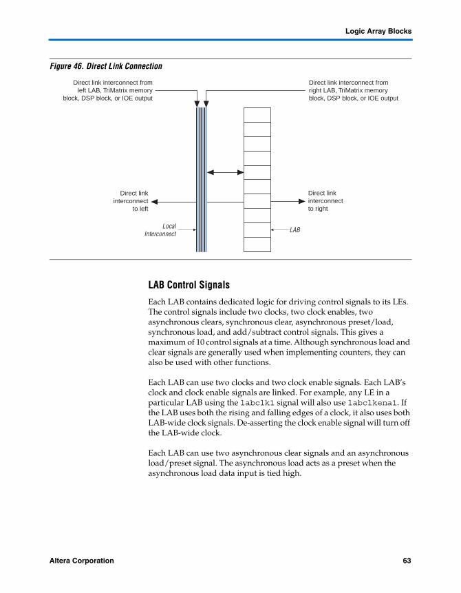
Logic Array Blocks
Figure 46. Direct Link Connection
LAB Control Signals
Each LAB contains dedicated logic for driving control signals to its LEs. The control signals include two clocks, two clock enables, two asynchronous clears, synchronous clear, asynchronous preset/load, synchronous load, and add/subtract control signals. This gives a maximum of 10 control signals at a time. Although synchronous load and clear signals are generally used when implementing counters, they can also be used with other functions.
Each LAB can use two clocks and two clock enable signals. Each LAB’s clock and clock enable signals are linked. For example, any LE in a particular LAB using the labclk1 signal will also use labclkena1. If the LAB uses both the rising and falling edges of a clock, it also uses both LAB-wide clock signals. De-asserting the clock enable signal will turn off the LAB-wide clock.
Each LAB can use two asynchronous clear signals and an asynchronous load/preset signal. The asynchronous load acts as a preset when the asynchronous load data input is tied high.
LAB
Direct linkinterconnectto right
Direct link interconnect fromright LAB, TriMatrix memoryblock, DSP block, or IOE output
Direct link interconnect fromleft LAB, TriMatrix memory
block, DSP block, or IOE output
LocalInterconnect
Direct linkinterconnect
to left
Altera Corporation 63Preliminary

Stratix GX FPGA Family
With the LAB-wide addnsub control signal, a single LE can implement a one-bit adder and subtractor. This saves LE resources and improves performance for logic functions such as DSP correlators and signed multipliers that alternate between addition and subtraction depending on data.
The LAB row clocks [7..0] and LAB local interconnect generate the LAB-wide control signals. The MultiTrackTM interconnect’s inherent low skew allows clock and control signal distribution in addition to data. Figure 47 shows the LAB control signal generation circuit.
Figure 47. LAB-Wide Control Signals
Logic Elements The smallest unit of logic in the Stratix GX architecture, the LE, is compact and provides advanced features with efficient logic utilization. Each LE contains a four-input LUT, which is a function generator that can implement any function of four variables. In addition, each LE contains a programmable register and carry chain with carry select capability. A single LE also supports dynamic single bit addition or subtraction mode selectable by an LAB-wide control signal. Each LE drives all types of interconnects: local, row, column, LUT chain, register chain, and direct link interconnects. See Figure 48.
labclkena1
labclk2labclk1
labclkena2
asyncloador labpre
syncload
DedicatedRow LABClocks
LocalInterconnect
LocalInterconnect
LocalInterconnect
LocalInterconnect
LocalInterconnect
LocalInterconnect
labclr1
labclr2
synclr
addnsub
8
64 Altera CorporationPreliminary
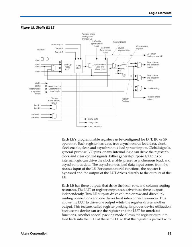
Logic Elements
Figure 48. Stratix GX LE
Each LE’s programmable register can be configured for D, T, JK, or SR operation. Each register has data, true asynchronous load data, clock, clock enable, clear, and asynchronous load/preset inputs. Global signals, general-purpose I/O pins, or any internal logic can drive the register’s clock and clear control signals. Either general-purpose I/O pins or internal logic can drive the clock enable, preset, asynchronous load, and asynchronous data. The asynchronous load data input comes from the data3 input of the LE. For combinatorial functions, the register is bypassed and the output of the LUT drives directly to the outputs of the LE.
Each LE has three outputs that drive the local, row, and column routing resources. The LUT or register output can drive these three outputs independently. Two LE outputs drive column or row and direct link routing connections and one drives local interconnect resources. This allows the LUT to drive one output while the register drives another output. This feature, called register packing, improves device utilization because the device can use the register and the LUT for unrelated functions. Another special packing mode allows the register output to feed back into the LUT of the same LE so that the register is packed with
labclk1
labclk2
labclr2labpre/aload
Carry-In1
Carry-In0
LAB Carry-In
Clock &Clock Enable
Select
LAB Carry-Out
Carry-Out1
Carry-Out0
Look-UpTable(LUT)
CarryChain
Row, column,and direct link routing
Row, column,and direct link routing
ProgrammableRegister
PRN/ALD
CLRN
D Q
ENA
Register Bypass
PackedRegister Select
Chip-WideReset
labclkena1labclkena2
SynchronousLoad andClear Logic
LAB-wideSynchronous
LoadLAB-wide
SynchronousClear
AsynchronousClear/Preset/Load Logic
data1
data2data3
data4
LUT chainrouting to next LE
labclr1
Local Routing
Register chainoutput
ADATA
addnsub
RegisterFeedback
Register chainrouting fromprevious LE
Altera Corporation 65Preliminary
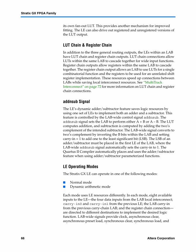
Stratix GX FPGA Family
its own fan-out LUT. This provides another mechanism for improved fitting. The LE can also drive out registered and unregistered versions of the LUT output.
LUT Chain & Register Chain
In addition to the three general routing outputs, the LEs within an LAB have LUT chain and register chain outputs. LUT chain connections allow LUTs within the same LAB to cascade together for wide input functions. Register chain outputs allow registers within the same LAB to cascade together. The register chain output allows an LAB to use LUTs for a single combinatorial function and the registers to be used for an unrelated shift register implementation. These resources speed up connections between LABs while saving local interconnect resources. See “MultiTrack Interconnect” on page 72 for more information on LUT chain and register chain connections.
addnsub Signal
The LE’s dynamic adder/subtractor feature saves logic resources by using one set of LEs to implement both an adder and a subtractor. This feature is controlled by the LAB-wide control signal addnsub. The addnsub signal sets the LAB to perform either A + B or A – B. The LUT computes addition, and subtraction is computed by adding the two’s complement of the intended subtractor. The LAB-wide signal converts to two’s complement by inverting the B bits within the LAB and setting carry-in = 1 to add one to the least significant bit (LSB). The LSB of an adder/subtractor must be placed in the first LE of the LAB, where the LAB-wide addnsub signal automatically sets the carry-in to 1. The Quartus II Compiler automatically places and uses the adder/subtractor feature when using adder/subtractor parameterized functions.
LE Operating Modes
The Stratix GX LE can operate in one of the following modes:
Normal mode Dynamic arithmetic mode
Each mode uses LE resources differently. In each mode, eight available inputs to the LE—the four data inputs from the LAB local interconnect; carry-in0 and carry-in1 from the previous LE; the LAB carry-in from the previous carry-chain LAB; and the register chain connection—are directed to different destinations to implement the desired logic function. LAB-wide signals provide clock, asynchronous clear, asynchronous preset load, synchronous clear, synchronous load, and
66 Altera CorporationPreliminary
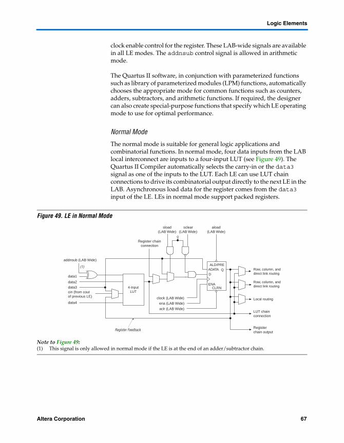
Logic Elements
clock enable control for the register. These LAB-wide signals are available in all LE modes. The addnsub control signal is allowed in arithmetic mode.
The Quartus II software, in conjunction with parameterized functions such as library of parameterized modules (LPM) functions, automatically chooses the appropriate mode for common functions such as counters, adders, subtractors, and arithmetic functions. If required, the designer can also create special-purpose functions that specify which LE operating mode to use for optimal performance.
Normal Mode
The normal mode is suitable for general logic applications and combinatorial functions. In normal mode, four data inputs from the LAB local interconnect are inputs to a four-input LUT (see Figure 49). The Quartus II Compiler automatically selects the carry-in or the data3 signal as one of the inputs to the LUT. Each LE can use LUT chain connections to drive its combinatorial output directly to the next LE in the LAB. Asynchronous load data for the register comes from the data3 input of the LE. LEs in normal mode support packed registers.
Figure 49. LE in Normal Mode
Note to Figure 49:(1) This signal is only allowed in normal mode if the LE is at the end of an adder/subtractor chain.
data1
4-InputLUT
data2
data3cin (from coutof previous LE)
data4
addnsub (LAB Wide)
clock (LAB Wide)
ena (LAB Wide)
aclr (LAB Wide)
aload(LAB Wide)
ALD/PRE
CLRN
DQ
ENA
ADATA
sclear(LAB Wide)
sload(LAB Wide)
Register chainconnection
LUT chainconnection
Registerchain output
Row, column, anddirect link routing
Row, column, anddirect link routing
Local routing
Register Feedback
(1)
Altera Corporation 67Preliminary

Stratix GX FPGA Family
Dynamic Arithmetic Mode
The dynamic arithmetic mode is ideal for implementing adders, counters, accumulators, wide parity functions, and comparators. An LE in dynamic arithmetic mode uses four 2-input LUTs configurable as a dynamic adder/subtractor. The first two 2-input LUTs compute two summations based on a possible carry-in of 1 or 0; the other two LUTs generate carry outputs for the two chains of the carry select circuitry. As shown in Figure 50, the LAB carry-in signal selects either the carry-in0 or carry-in1 chain. The selected chain’s logic level in turn determines which parallel sum is generated as a combinatorial or registered output. For example, when implementing an adder, the sum output is the selection of two possible calculated sums: data1 + data2 + carry-in0 or data1 + data2 + carry-in1. The other two LUTs use the data1 and data2 signals to generate two possible carry-out signals—one for a carry of 1 and the other for a carry of 0. The carry-in0 signal acts as the carry select for the carry-out0 output and carry-in1 acts as the carry select for the carry-out1 output. LEs in arithmetic mode can drive out registered and unregistered versions of the LUT output.
The dynamic arithmetic mode also offers clock enable, counter enable, synchronous up/down control, synchronous clear, synchronous load, and dynamic adder/subtractor options. The LAB local interconnect data inputs generate the counter enable and synchronous up/down control signals. The synchronous clear and synchronous load options are LAB-wide signals that affect all registers in the LAB. The Quartus II software automatically places any registers that are not used by the counter into other LABs. The addnsub LAB-wide signal controls whether the LE acts as an adder or subtractor.
68 Altera CorporationPreliminary
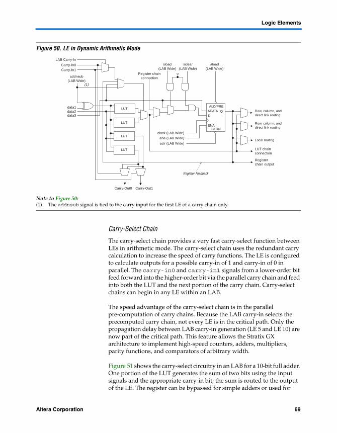
Logic Elements
Figure 50. LE in Dynamic Arithmetic Mode
Note to Figure 50:(1) The addnsub signal is tied to the carry input for the first LE of a carry chain only.
Carry-Select Chain
The carry-select chain provides a very fast carry-select function between LEs in arithmetic mode. The carry-select chain uses the redundant carry calculation to increase the speed of carry functions. The LE is configured to calculate outputs for a possible carry-in of 1 and carry-in of 0 in parallel. The carry-in0 and carry-in1 signals from a lower-order bit feed forward into the higher-order bit via the parallel carry chain and feed into both the LUT and the next portion of the carry chain. Carry-select chains can begin in any LE within an LAB.
The speed advantage of the carry-select chain is in the parallel pre-computation of carry chains. Because the LAB carry-in selects the precomputed carry chain, not every LE is in the critical path. Only the propagation delay between LAB carry-in generation (LE 5 and LE 10) are now part of the critical path. This feature allows the Stratix GX architecture to implement high-speed counters, adders, multipliers, parity functions, and comparators of arbitrary width.
Figure 51 shows the carry-select circuitry in an LAB for a 10-bit full adder. One portion of the LUT generates the sum of two bits using the input signals and the appropriate carry-in bit; the sum is routed to the output of the LE. The register can be bypassed for simple adders or used for
data1 LUTdata2data3
addnsub(LAB Wide)
clock (LAB Wide)
ena (LAB Wide)
aclr (LAB Wide)
ALD/PRE
CLRN
DQ
ENA
ADATA
Register chainconnection
LUT
LUT
LUT
Carry-Out1Carry-Out0
LAB Carry-In
Carry-In0Carry-In1
(1)
sclear(LAB Wide)
sload(LAB Wide)
LUT chainconnection
Registerchain output
Row, column, anddirect link routing
Row, column, anddirect link routing
Local routing
aload(LAB Wide)
Register Feedback
Altera Corporation 69Preliminary
Stratix GX FPGA Family
accumulator functions. Another portion of the LUT generates carry-out bits. An LAB-wide carry in bit selects which chain is used for the addition of given inputs. The carry-in signal for each chain, carry-in0 or carry-in1, selects the carry-out to carry forward to the carry-in signal of the next-higher-order bit. The final carry-out signal is routed to an LE, where it is fed to local, row, or column interconnects.
The Quartus II Compiler automatically creates carry chain logic during design processing, or the designer can create it manually during design entry. Parameterized functions such as LPM functions automatically take advantage of carry chains for the appropriate functions.
The Quartus II Compiler creates carry chains longer than 10 LEs by linking LABs together automatically. For enhanced fitting, a long carry chain runs vertically allowing fast horizontal connections to TriMatrix memory and DSP blocks. A carry chain can continue as far as a full column.
70 Altera CorporationPreliminary

Logic Elements
Figure 51. Carry Select Chain
Clear & Preset Logic Control
LAB-wide signals control the logic for the register’s clear and preset signals. The LE directly supports an asynchronous clear and preset function. The register preset is achieved through the asynchronous load of a logic high. The direct asynchronous preset does not require a NOT-gate push-back technique. Stratix GX devices support simultaneous preset/ asynchronous load, and clear signals. An asynchronous clear signal takes precedence if both signals are asserted simultaneously. Each LAB supports up to two clears and one preset signal.
In addition to the clear and preset ports, Stratix GX devices provide a chip-wide reset pin (DEV_CLRn) that resets all registers in the device. An option set before compilation in the Quartus II software controls this pin. This chip-wide reset overrides all other control signals.
LE4
LE3
LE2
LE1A1B1
A2B2
A3B3
A4B4
Sum1
Sum2
Sum3
Sum4
LE10
LE9
LE8
LE7A7B7
A8B8
A9B9
A10B10
Sum7
LE6A6B6
Sum6
LE5A5B5
Sum5
Sum8
Sum9
Sum10
0 1
0 1LAB Carry-In
LAB Carry-Out
LUT
LUT
LUT
LUT
data1
LAB Carry-In
data2
Carry-In0
Carry-In1
Carry-Out0 Carry-Out1
Sum
Altera Corporation 71Preliminary
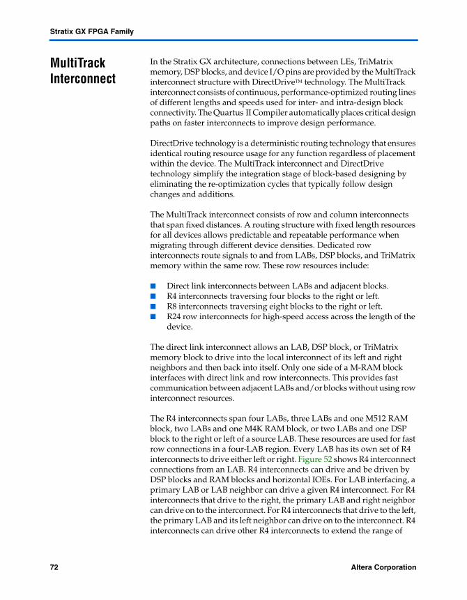
Stratix GX FPGA Family
MultiTrack Interconnect
In the Stratix GX architecture, connections between LEs, TriMatrix memory, DSP blocks, and device I/O pins are provided by the MultiTrack interconnect structure with DirectDriveTM technology. The MultiTrack interconnect consists of continuous, performance-optimized routing lines of different lengths and speeds used for inter- and intra-design block connectivity. The Quartus II Compiler automatically places critical design paths on faster interconnects to improve design performance.
DirectDrive technology is a deterministic routing technology that ensures identical routing resource usage for any function regardless of placement within the device. The MultiTrack interconnect and DirectDrive technology simplify the integration stage of block-based designing by eliminating the re-optimization cycles that typically follow design changes and additions.
The MultiTrack interconnect consists of row and column interconnects that span fixed distances. A routing structure with fixed length resources for all devices allows predictable and repeatable performance when migrating through different device densities. Dedicated row interconnects route signals to and from LABs, DSP blocks, and TriMatrix memory within the same row. These row resources include:
Direct link interconnects between LABs and adjacent blocks. R4 interconnects traversing four blocks to the right or left. R8 interconnects traversing eight blocks to the right or left. R24 row interconnects for high-speed access across the length of the
device.
The direct link interconnect allows an LAB, DSP block, or TriMatrix memory block to drive into the local interconnect of its left and right neighbors and then back into itself. Only one side of a M-RAM block interfaces with direct link and row interconnects. This provides fast communication between adjacent LABs and/or blocks without using row interconnect resources.
The R4 interconnects span four LABs, three LABs and one M512 RAM block, two LABs and one M4K RAM block, or two LABs and one DSP block to the right or left of a source LAB. These resources are used for fast row connections in a four-LAB region. Every LAB has its own set of R4 interconnects to drive either left or right. Figure 52 shows R4 interconnect connections from an LAB. R4 interconnects can drive and be driven by DSP blocks and RAM blocks and horizontal IOEs. For LAB interfacing, a primary LAB or LAB neighbor can drive a given R4 interconnect. For R4 interconnects that drive to the right, the primary LAB and right neighbor can drive on to the interconnect. For R4 interconnects that drive to the left, the primary LAB and its left neighbor can drive on to the interconnect. R4 interconnects can drive other R4 interconnects to extend the range of
72 Altera CorporationPreliminary
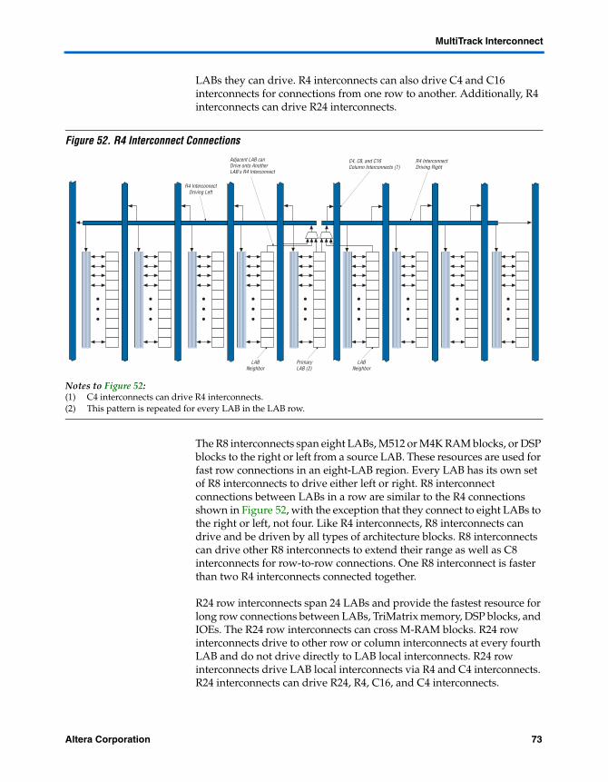
MultiTrack Interconnect
LABs they can drive. R4 interconnects can also drive C4 and C16 interconnects for connections from one row to another. Additionally, R4 interconnects can drive R24 interconnects.
Figure 52. R4 Interconnect Connections
Notes to Figure 52:(1) C4 interconnects can drive R4 interconnects.(2) This pattern is repeated for every LAB in the LAB row.
The R8 interconnects span eight LABs, M512 or M4K RAM blocks, or DSP blocks to the right or left from a source LAB. These resources are used for fast row connections in an eight-LAB region. Every LAB has its own set of R8 interconnects to drive either left or right. R8 interconnect connections between LABs in a row are similar to the R4 connections shown in Figure 52, with the exception that they connect to eight LABs to the right or left, not four. Like R4 interconnects, R8 interconnects can drive and be driven by all types of architecture blocks. R8 interconnects can drive other R8 interconnects to extend their range as well as C8 interconnects for row-to-row connections. One R8 interconnect is faster than two R4 interconnects connected together.
R24 row interconnects span 24 LABs and provide the fastest resource for long row connections between LABs, TriMatrix memory, DSP blocks, and IOEs. The R24 row interconnects can cross M-RAM blocks. R24 row interconnects drive to other row or column interconnects at every fourth LAB and do not drive directly to LAB local interconnects. R24 row interconnects drive LAB local interconnects via R4 and C4 interconnects. R24 interconnects can drive R24, R4, C16, and C4 interconnects.
PrimaryLAB (2)
R4 InterconnectDriving Left
Adjacent LAB canDrive onto AnotherLAB's R4 Interconnect
C4, C8, and C16Column Interconnects (1)
R4 InterconnectDriving Right
LABNeighbor
LABNeighbor
Altera Corporation 73Preliminary

Stratix GX FPGA Family
The column interconnect operates similarly to the row interconnect and vertically routes signals to and from LABs, TriMatrix memory, DSP blocks, and IOEs. Each column of LABs is served by a dedicated column interconnect, which vertically routes signals to and from LABs, TriMatrix memory and DSP blocks, and horizontal IOEs. These column resources include:
LUT chain interconnects within an LAB Register chain interconnects within an LAB C4 interconnects traversing a distance of four blocks in up and down
direction C8 interconnects traversing a distance of eight blocks in up and
down direction C16 column interconnects for high-speed vertical routing through
the device
Stratix GX devices include an enhanced interconnect structure within LABs for routing LE output to LE input connections faster using LUT chain connections and register chain connections. The LUT chain connection allows the combinatorial output of an LE to directly drive the fast input of the LE right below it, bypassing the local interconnect. These resources can be used as a high-speed connection for wide fan-in functions from LE 1 to LE 10 in the same LAB. The register chain connection allows the register output of one LE to connect directly to the register input of the next LE in the LAB for fast shift registers. The Quartus II Compiler automatically takes advantage of these resources to improve utilization and performance. Figure 53 shows the LUT chain and register chain interconnects.
74 Altera CorporationPreliminary

MultiTrack Interconnect
Figure 53. LUT Chain & Register Chain Interconnects
The C4 interconnects span four LABs, M512, or M4K blocks up or down from a source LAB. Every LAB has its own set of C4 interconnects to drive either up or down. Figure 54 shows the C4 interconnect connections from an LAB in a column. The C4 interconnects can drive and be driven by all types of architecture blocks, including DSP blocks, TriMatrix memory blocks, and vertical IOEs. For LAB interconnection, a primary LAB or its LAB neighbor can drive a given C4 interconnect. C4 interconnects can drive each other to extend their range as well as drive row interconnects for column-to-column connections.
LE 1
LE 2
LE 3
LE 4
LE 5
LE 6
LE 7
LE 8
LE 9
LE 10
LUT ChainRouting to
Adjacent LE
LocalInterconnect
Register ChainRouting to AdjacentLE's Register Input
Local InterconnectRouting Among LEsin the LAB
Altera Corporation 75Preliminary

Stratix GX FPGA Family
Figure 54. C4 Interconnect Connections Note (1)
Note to Figure 54:(1) Each C4 interconnect can drive either up or down four rows.
C8 interconnects span eight LABs, M512, or M4K blocks up or down from a source LAB. Every LAB has its own set of C8 interconnects to drive either up or down. C8 interconnect connections between the LABs in a column are similar to the C4 connections shown in Figure 54 with the exception that they connect to eight LABs above and below. The C8
C4 InterconnectDrives Local and R4Interconnectsup to Four Rows
Adjacent LAB candrive onto neighboringLAB's C4 interconnect
C4 InterconnectDriving Up
C4 InterconnectDriving Down
LAB
RowInterconnect
LocalInterconnect
76 Altera CorporationPreliminary

MultiTrack Interconnect
interconnects can drive and be driven by all types of architecture blocks similar to C4 interconnects. C8 interconnects can drive each other to extend their range as well as R8 interconnects for column-to-column connections. C8 interconnects are faster than two C4 interconnects.
C16 column interconnects span a length of 16 LABs and provide the fastest resource for long column connections between LABs, TriMatrix memory blocks, DSP blocks, and IOEs. C16 interconnects can cross M-RAM blocks and also drive to row and column interconnects at every fourth LAB. C16 interconnects drive LAB local interconnects via C4 and R4 interconnects and do not drive LAB local interconnects directly.
All embedded blocks communicate with the logic array similar to LAB-to-LAB interfaces. Each block (i.e., TriMatrix memory and DSP blocks) connects to row and column interconnects and has local interconnect regions driven by row and column interconnects. These blocks also have direct link interconnects for fast connections to and from a neighboring LAB. All blocks are fed by the row LAB clocks, labclk[7..0].
Altera Corporation 77Preliminary
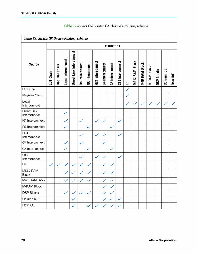
Stratix GX FPGA Family
Table 22 shows the Stratix GX device’s routing scheme.
Table 22. Stratix GX Device Routing Scheme
Source
DestinationLU
T Ch
ain
Regi
ster
Cha
in
Loca
l Int
erco
nnec
t
Dire
ct L
ink
Inte
rcon
nect
R4 In
terc
onne
ct
R8 In
terc
onne
ct
R24
Inte
rcon
nect
C4 In
terc
onne
ct
C8 In
terc
onne
ct
C16
Inte
rcon
nect
LE M51
2 RA
M B
lock
M4K
RAM
Blo
ck
M-R
AM B
lock
DSP
Bloc
ks
Colu
mn
IOE
Row
IOE
LUT Chain v
Register Chain v
Local Interconnect v v v v v v v
Direct Link Interconnect v
R4 Interconnect v v v v v
R8 Interconnect v v v
R24 Interconnect v v v v
C4 Interconnect v v v
C8 Interconnect v v v
C16 Interconnect v v v v
LE v v v v v v v v
M512 RAM Block v v v v v v
M4K RAM Block v v v v v v
M-RAM Block v v
DSP Blocks v v v v v v
Column IOE v v v v
Row IOE v v v v v v
78 Altera CorporationPreliminary
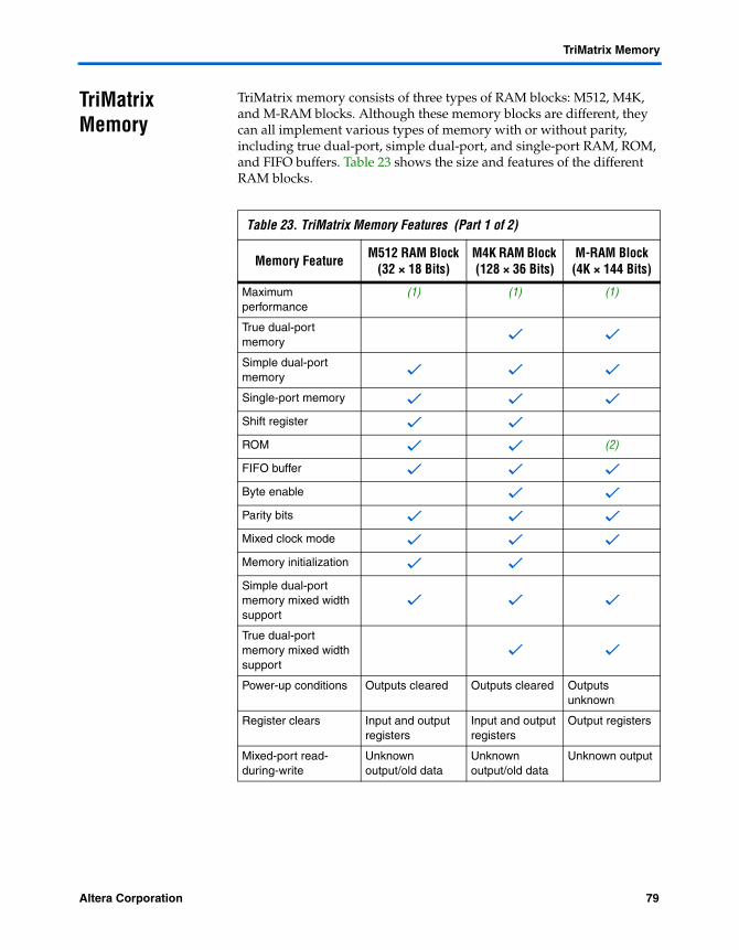
TriMatrix Memory
TriMatrix Memory
TriMatrix memory consists of three types of RAM blocks: M512, M4K, and M-RAM blocks. Although these memory blocks are different, they can all implement various types of memory with or without parity, including true dual-port, simple dual-port, and single-port RAM, ROM, and FIFO buffers. Table 23 shows the size and features of the different RAM blocks.
Table 23. TriMatrix Memory Features (Part 1 of 2)
Memory Feature M512 RAM Block (32 × 18 Bits)
M4K RAM Block (128 × 36 Bits)
M-RAM Block (4K × 144 Bits)
Maximum performance
(1) (1) (1)
True dual-port memory v v
Simple dual-port memory v v v
Single-port memory v v v
Shift register v v
ROM v v (2)
FIFO buffer v v v
Byte enable v v
Parity bits v v v
Mixed clock mode v v v
Memory initialization v v
Simple dual-port memory mixed width support
v v v
True dual-port memory mixed width support
v v
Power-up conditions Outputs cleared Outputs cleared Outputs unknown
Register clears Input and output registers
Input and output registers
Output registers
Mixed-port read-during-write
Unknown output/old data
Unknown output/old data
Unknown output
Altera Corporation 79Preliminary
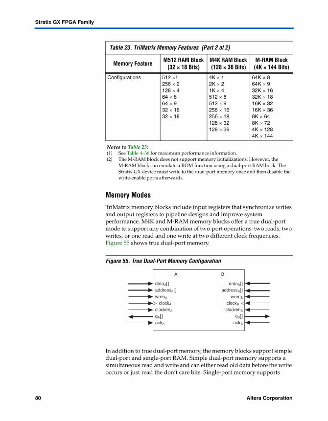
Stratix GX FPGA Family
Memory Modes
TriMatrix memory blocks include input registers that synchronize writes and output registers to pipeline designs and improve system performance. M4K and M-RAM memory blocks offer a true dual-port mode to support any combination of two-port operations: two reads, two writes, or one read and one write at two different clock frequencies. Figure 55 shows true dual-port memory.
Figure 55. True Dual-Port Memory Configuration
In addition to true dual-port memory, the memory blocks support simple dual-port and single-port RAM. Simple dual-port memory supports a simultaneous read and write and can either read old data before the write occurs or just read the don’t care bits. Single-port memory supports
Configurations 512 ×1256 × 2128 × 464 × 864 × 932 × 1632 × 18
4K × 12K × 21K × 4512 × 8512 × 9256 × 16256 × 18128 × 32128 × 36
64K × 864K × 932K × 1632K × 1816K × 3216K × 368K × 648K × 724K × 1284K × 144
Notes to Table 23:(1) See Table 4–36 for maximum performance information.(2) The M-RAM block does not support memory initializations. However, the
M-RAM block can emulate a ROM function using a dual-port RAM bock. The Stratix GX device must write to the dual-port memory once and then disable the write-enable ports afterwards.
Table 23. TriMatrix Memory Features (Part 2 of 2)
Memory Feature M512 RAM Block (32 × 18 Bits)
M4K RAM Block (128 × 36 Bits)
M-RAM Block (4K × 144 Bits)
dataA[ ]addressA[ ]wrenA
clockA
clockenA
qA[ ]aclrA
dataB[ ]addressB[ ]
wrenB
clockB clockenB
qB[ ]aclrB
A B
80 Altera CorporationPreliminary

TriMatrix Memory
non-simultaneous reads and writes, but the q[] port will output the data once it has been written to the memory (if the outputs are not registered) or after the next rising edge of the clock (if the outputs are registered). For more information, see the chapter TriMatrix Embedded Memory Blocks in Stratix & Stratix GX Devices of the Stratix Device Handbook, Volume 2. Figure 56 shows these different RAM memory port configurations for TriMatrix memory.
Figure 56. Simple Dual-Port & Single-Port Memory Configurations
Note to Figure 56:(1) Two single-port memory blocks can be implemented in a single M4K block as long
as each of the two independent block sizes is equal to or less than half of the M4K block size.
The memory blocks also enable mixed-width data ports for reading and writing to the RAM ports in dual-port RAM configuration. For example, the memory block can be written in ×1 mode at port A and read out in ×16 mode from port B.
TriMatrix memory architecture can implement pipelined RAM by registering both the input and output signals to the RAM block. All TriMatrix memory block inputs are registered providing synchronous write cycles. In synchronous operation, the memory block generates its own self-timed strobe write enable (WREN) signal derived from the global or regional clock. In contrast, a circuit using asynchronous RAM must
data[ ]wraddress[ ]wren inclockinclockeninaclr
rdaddress[ ]rden
q[ ]outclock outclocken
outaclr
data[ ]address[ ]wren inclockinclockeninaclr
q[ ]outclock outclocken
outaclr
Single-Port Memory (1)
Simple Dual-Port Memory
Altera Corporation 81Preliminary
Stratix GX FPGA Family
generate the RAM WREN signal while ensuring its data and address signals meet setup and hold time specifications relative to the WREN signal. The output registers can be bypassed. Flow-through reading is possible in the simple dual-port mode of M512 and M4K RAM blocks by clocking the read enable and read address registers on the negative clock edge and bypassing the output registers.
Two single-port memory blocks can be implemented in a single M4K block as long as each of the two independent block sizes is equal to or less than half of the M4K block size.
The Quartus II software automatically implements larger memory by combining multiple TriMatrix memory blocks. For example, two 256 × 16-bit RAM blocks can be combined to form a 256 × 32-bit RAM block. Memory performance does not degrade for memory blocks using the maximum number of words available in one memory block. Logical memory blocks using less than the maximum number of words use physical blocks in parallel, eliminating any external control logic that would increase delays. To create a larger high-speed memory block, the Quartus II software automatically combines memory blocks with LE control logic.
Parity Bit Support
The memory blocks support a parity bit for each byte. The parity bit, along with internal LE logic, can implement parity checking for error detection to ensure data integrity. Designers can also use parity-size data words to store user-specified control bits. In the M4K and M-RAM blocks, byte enables are also available for data input masking during write operations.
Shift Register Support
The designer can configure embedded memory blocks to implement shift registers for DSP applications such as pseudo-random number generators, multi-channel filtering, auto-correlation, and cross-correlation functions. These and other DSP applications require local data storage, traditionally implemented with standard flip-flops, which can quickly consume many logic cells and routing resources for large shift registers. A more efficient alternative is to use embedded memory as a shift register block, which saves logic cell and routing resources and provides a more efficient implementation with the dedicated circuitry.
The size of a w × m × n shift register is determined by the input data width (w), the length of the taps (m), and the number of taps (n). The size of a w × m × n shift register must be less than or equal to the maximum number of memory bits in the respective block: 576 bits for the M512
82 Altera CorporationPreliminary
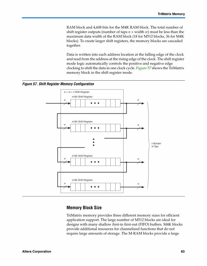
TriMatrix Memory
RAM block and 4,608 bits for the M4K RAM block. The total number of shift register outputs (number of taps n × width w) must be less than the maximum data width of the RAM block (18 for M512 blocks, 36 for M4K blocks). To create larger shift registers, the memory blocks are cascaded together.
Data is written into each address location at the falling edge of the clock and read from the address at the rising edge of the clock. The shift register mode logic automatically controls the positive and negative edge clocking to shift the data in one clock cycle. Figure 57 shows the TriMatrix memory block in the shift register mode.
Figure 57. Shift Register Memory Configuration
Memory Block Size
TriMatrix memory provides three different memory sizes for efficient application support. The large number of M512 blocks are ideal for designs with many shallow first-in first-out (FIFO) buffers. M4K blocks provide additional resources for channelized functions that do not require large amounts of storage. The M-RAM blocks provide a large
m-Bit Shift Registerw w
m-Bit Shift Register
m-Bit Shift Register
m-Bit Shift Register
w w
w w
w w
w × m × n Shift Register
n Numberof Taps
Altera Corporation 83Preliminary
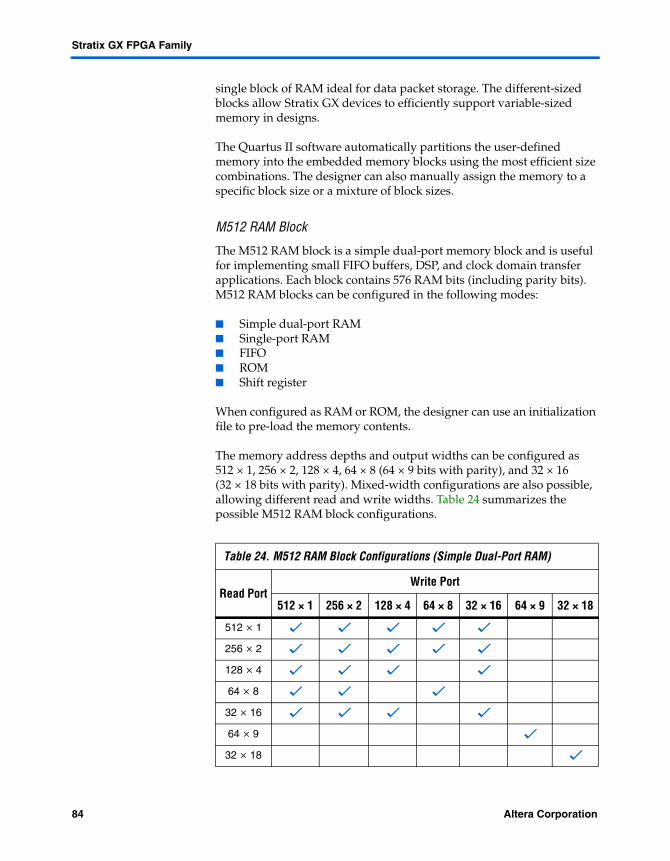
Stratix GX FPGA Family
single block of RAM ideal for data packet storage. The different-sized blocks allow Stratix GX devices to efficiently support variable-sized memory in designs.
The Quartus II software automatically partitions the user-defined memory into the embedded memory blocks using the most efficient size combinations. The designer can also manually assign the memory to a specific block size or a mixture of block sizes.
M512 RAM Block
The M512 RAM block is a simple dual-port memory block and is useful for implementing small FIFO buffers, DSP, and clock domain transfer applications. Each block contains 576 RAM bits (including parity bits). M512 RAM blocks can be configured in the following modes:
Simple dual-port RAM Single-port RAM FIFO ROM Shift register
When configured as RAM or ROM, the designer can use an initialization file to pre-load the memory contents.
The memory address depths and output widths can be configured as 512 × 1, 256 × 2, 128 × 4, 64 × 8 (64 × 9 bits with parity), and 32 × 16 (32 × 18 bits with parity). Mixed-width configurations are also possible, allowing different read and write widths. Table 24 summarizes the possible M512 RAM block configurations.
Table 24. M512 RAM Block Configurations (Simple Dual-Port RAM)
Read PortWrite Port
512 × 1 256 × 2 128 × 4 64 × 8 32 × 16 64 × 9 32 × 18
512 × 1 v v v v v
256 × 2 v v v v v
128 × 4 v v v v
64 × 8 v v v
32 × 16 v v v v
64 × 9 v
32 × 18 v
84 Altera CorporationPreliminary

TriMatrix Memory
When the M512 RAM block is configured as a shift register block, a shift register of size up to 576 bits is possible.
The M512 RAM block can also be configured to support serializer and deserializer applications. By using the mixed-width support in combination with DDR I/O standards, the block can function as a SERDES to support low-speed serial I/O standards using global or regional clocks. See “I/O Structure” on page 157 for details on dedicated SERDES in Stratix GX devices.
M512 RAM blocks can have different clocks on its inputs and outputs. The wren, datain, and write address registers are all clocked together from one of the two clocks feeding the block. The read address, rden, and output registers can be clocked by either of the two clocks driving the block. This allows the RAM block to operate in read/write or input/output clock modes. Only the output register can be bypassed. The eight labclk signals or local interconnect can drive the inclock, outclock, wren, rden, inclr, and outclr signals. Because of the advanced interconnect between the LAB and M512 RAM blocks, LEs can also control the wren and rden signals and the RAM clock, clock enable, and asynchronous clear signals. Figure 58 shows the M512 RAM block control signal generation logic.
The RAM blocks within Stratix GX devices have local interconnects to allow LEs and interconnects to drive into RAM blocks. The M512 RAM block local interconnect is driven by the R4, R8, C4, C8, and direct link interconnects from adjacent LABs. The M512 RAM blocks can communicate with LABs on either the left or right side through these row interconnects or with LAB columns on the left or right side with the column interconnects. Up to 10 direct link input connections to the M512 RAM block are possible from the left adjacent LABs and another 10 possible from the right adjacent LAB. M512 RAM outputs can also connect to left and right LABs through 10 direct link interconnects. The M512 RAM block has equal opportunity for access and performance to and from LABs on either its left or right side. Figure 59 shows the M512 RAM block to logic array interface.
Altera Corporation 85Preliminary
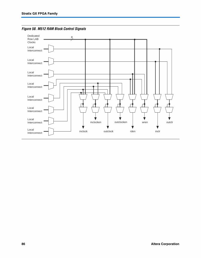
Stratix GX FPGA Family
Figure 58. M512 RAM Block Control Signals
inclocken
outclockinclock
outclocken
rden
wren
DedicatedRow LABClocks
LocalInterconnect
LocalInterconnect
LocalInterconnect
LocalInterconnect
LocalInterconnect
LocalInterconnect
inclr
outclr
8
LocalInterconnect
LocalInterconnect
86 Altera CorporationPreliminary

TriMatrix Memory
Figure 59. M512 RAM Block LAB Row Interface
M4K RAM Blocks
The M4K RAM block includes support for true dual-port RAM. The M4K RAM block is used to implement buffers for a wide variety of applications such as storing processor code, implementing lookup schemes, and implementing larger memory applications. Each block contains 4,608 RAM bits (including parity bits). M4K RAM blocks can be configured in the following modes:
True dual-port RAM Simple dual-port RAM Single-port RAM FIFO ROM Shift register
When configured as RAM or ROM, the designer can use an initialization file to pre-load the memory contents.
dataout
M512 RAMBlock
datain
Clocks
10
Direct link interconnectfrom adjacent LAB
Direct link interconnectto adjacent LAB
Direct link interconnectfrom adjacent LAB
Direct link interconnectto adjacent LAB
Small RAM Block LocalInterconnect Region
C4 and C8Interconnects R4 and R8
Interconnects
ControlSignals
address
LAB Row Clocks
2
8
Altera Corporation 87Preliminary
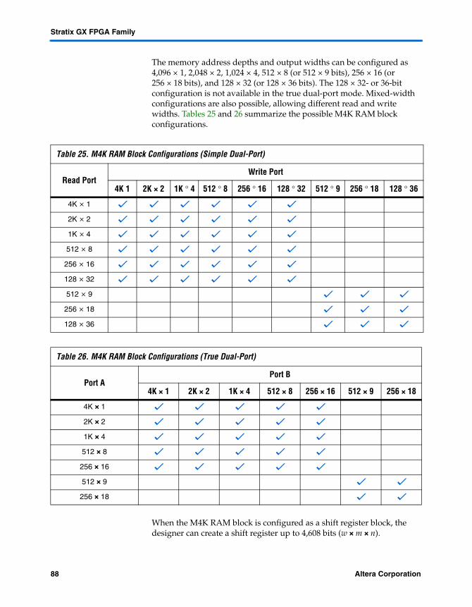
Stratix GX FPGA Family
The memory address depths and output widths can be configured as 4,096 × 1, 2,048 × 2, 1,024 × 4, 512 × 8 (or 512 × 9 bits), 256 × 16 (or 256 × 18 bits), and 128 × 32 (or 128 × 36 bits). The 128 × 32- or 36-bit configuration is not available in the true dual-port mode. Mixed-width configurations are also possible, allowing different read and write widths. Tables 25 and 26 summarize the possible M4K RAM block configurations.
When the M4K RAM block is configured as a shift register block, the designer can create a shift register up to 4,608 bits (w × m × n).
Table 25. M4K RAM Block Configurations (Simple Dual-Port)
Read PortWrite Port
4K 1 2K × 2 1K ° 4 512 ° 8 256 ° 16 128 ° 32 512 ° 9 256 ° 18 128 ° 36
4K × 1 v v v v v v
2K × 2 v v v v v v
1K × 4 v v v v v v
512 × 8 v v v v v v
256 × 16 v v v v v v
128 × 32 v v v v v v
512 × 9 v v v
256 × 18 v v v
128 × 36 v v v
Table 26. M4K RAM Block Configurations (True Dual-Port)
Port APort B
4K × 1 2K × 2 1K × 4 512 × 8 256 × 16 512 × 9 256 × 18
4K × 1 v v v v v
2K × 2 v v v v v
1K × 4 v v v v v
512 × 8 v v v v v
256 × 16 v v v v v
512 × 9 v v
256 × 18 v v
88 Altera CorporationPreliminary

TriMatrix Memory
M4K RAM blocks support byte writes when the write port has a data width of 16, 18, 32, or 36 bits. The byte enables allow the input data to be masked so the device can write to specific bytes. The unwritten bytes retain the previous written value. Table 27 summarizes the byte selection.
The M4K RAM blocks allow for different clocks on their inputs and outputs. Either of the two clocks feeding the block can clock M4K RAM block registers (renwe, address, byte enable, datain, and output registers). Only the output register can be bypassed. The eight labclk signals or local interconnects can drive the control signals for the A and B ports of the M4K RAM block. LEs can also control the clock_a, clock_b, renwe_a, renwe_b, clr_a, clr_b, clocken_a, and clocken_b signals, as shown in Figure 60.
The R4, R8, C4, C8, and direct link interconnects from adjacent LABs drive the M4K RAM block local interconnect. The M4K RAM blocks can communicate with LABs on either the left or right side through these row resources or with LAB columns on either the right or left with the column resources. Up to 10 direct link input connections to the M4K RAM Block are possible from the left adjacent LABs and another 10 possible from the right adjacent LAB. M4K RAM block outputs can also connect to left and right LABs through 10 direct link interconnects each. Figure 61 shows the M4K RAM block to logic array interface.
Table 27. Byte Enable for M4K Blocks Notes (1), (2)
byteena[3..0] datain ×18 datain ×36
[0] = 1 [8..0] [8..0]
[1] = 1 [17..9] [17..9]
[2] = 1 – [26..18]
[3] = 1 – [35..27]
Notes to Table 27:(1) Any combination of byte enables is possible.(2) Byte enables can be used in the same manner with 8-bit words, i.e., in ×16 and ×32
modes.
Altera Corporation 89Preliminary
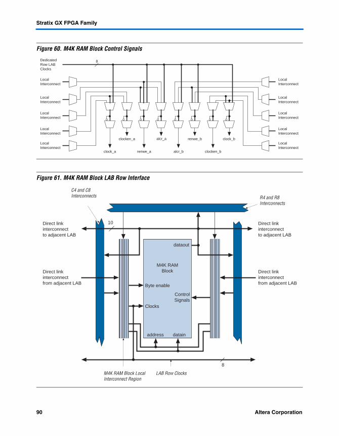
Stratix GX FPGA Family
Figure 60. M4K RAM Block Control Signals
Figure 61. M4K RAM Block LAB Row Interface
clocken_a
renwe_aclock_a
alcr_a
alcr_b
renwe_b
DedicatedRow LABClocks
LocalInterconnect
LocalInterconnect
LocalInterconnect
LocalInterconnect
LocalInterconnect
clocken_b
clock_b
8
LocalInterconnect
LocalInterconnect
LocalInterconnect
LocalInterconnect
LocalInterconnect
dataout
M4K RAMBlock
datainaddress
10
Direct link interconnectfrom adjacent LAB
Direct link interconnectto adjacent LAB
Direct link interconnectfrom adjacent LAB
Direct link interconnectto adjacent LAB
M4K RAM Block LocalInterconnect Region
C4 and C8Interconnects R4 and R8
Interconnects
LAB Row Clocks
Clocks
Byte enable
ControlSignals
8
90 Altera CorporationPreliminary
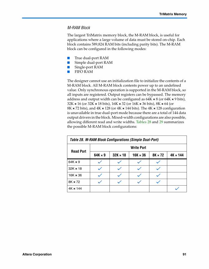
TriMatrix Memory
M-RAM Block
The largest TriMatrix memory block, the M-RAM block, is useful for applications where a large volume of data must be stored on-chip. Each block contains 589,824 RAM bits (including parity bits). The M-RAM block can be configured in the following modes:
True dual-port RAM Simple dual-port RAM Single-port RAM FIFO RAM
The designer cannot use an initialization file to initialize the contents of a M-RAM block. All M-RAM block contents power up to an undefined value. Only synchronous operation is supported in the M-RAM block, so all inputs are registered. Output registers can be bypassed. The memory address and output width can be configured as 64K × 8 (or 64K × 9 bits), 32K × 16 (or 32K × 18 bits), 16K × 32 (or 16K × 36 bits), 8K × 64 (or 8K × 72 bits), and 4K × 128 (or 4K × 144 bits). The 4K × 128 configuration is unavailable in true dual-port mode because there are a total of 144 data output drivers in the block. Mixed-width configurations are also possible, allowing different read and write widths. Tables 28 and 29 summarizes the possible M-RAM block configurations:
Table 28. M-RAM Block Configurations (Simple Dual-Port)
Read PortWrite Port
64K × 9 32K × 18 16K × 36 8K × 72 4K × 144
64K × 9 v v v v
32K × 18 v v v v
16K × 36 v v v v
8K × 72 v v v v
4K × 144 v
Altera Corporation 91Preliminary
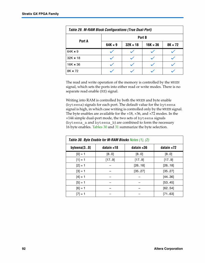
Stratix GX FPGA Family
The read and write operation of the memory is controlled by the WREN signal, which sets the ports into either read or write modes. There is no separate read enable (RE) signal.
Writing into RAM is controlled by both the WREN and byte enable (byteena) signals for each port. The default value for the byteena signal is high, in which case writing is controlled only by the WREN signal. The byte enables are available for the ×18, ×36, and ×72 modes. In the ×144 simple dual-port mode, the two sets of byteena signals (byteena_a and byteena_b) are combined to form the necessary 16 byte enables. Tables 30 and 31 summarize the byte selection.
Table 29. M-RAM Block Configurations (True Dual-Port)
Port APort B
64K × 9 32K × 18 16K × 36 8K × 72
64K × 9 v v v v
32K × 18 v v v v
16K × 36 v v v v
8K × 72 v v v v
Table 30. Byte Enable for M-RAM Blocks Notes (1), (2)
byteena[3..0] datain ×18 datain ×36 datain ×72
[0] = 1 [8..0] [8..0] [8..0]
[1] = 1 [17..9] [17..9] [17..9]
[2] = 1 – [26..18] [26..18]
[3] = 1 – [35..27] [35..27]
[4] = 1 – – [44..36]
[5] = 1 – – [53..45]
[6] = 1 – – [62..54]
[7] = 1 – – [71..63]
92 Altera CorporationPreliminary

TriMatrix Memory
Similar to all RAM blocks, M-RAM blocks can have different clocks on their inputs and outputs. All input registers—renwe, datain, address, and byte enable registers—are clocked together from either of the two clocks feeding the block. The output register can be bypassed. The eight labclk signals or local interconnect can drive the control signals for the A and B ports of the M-RAM block. LEs can also control the clock_a, clock_b, renwe_a, renwe_b, clr_a, clr_b, clocken_a, and clocken_b signals as shown in Figure 62.
Table 31. M-RAM Combined Byte Selection for ×144 Mode Notes (1), (2)
byteena[15..0] datain ×144
[0] = 1 [8..0]
[1] = 1 [17..9]
[2] = 1 [26..18]
[3] = 1 [35..27]
[4] = 1 [44..36]
[5] = 1 [53..45]
[6] = 1 [62..54]
[7] = 1 [71..63]
[8] = 1 [80..72]
[9] = 1 [89..81]
[10] = 1 [98..90]
[11] = 1 [107..99]
[12] = 1 [116..108]
[13] = 1 [125..117]
[14] = 1 [134..126]
[15] = 1 [143..135]
Notes to Tables 30 and 31:(1) Any combination of byte enables is possible.(2) Byte enables can be used in the same manner with 8-bit words, i.e., in ×16, ×32,
×64, and ×128 modes.
Altera Corporation 93Preliminary
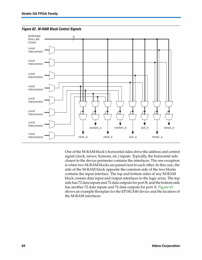
Stratix GX FPGA Family
Figure 62. M-RAM Block Control Signals
One of the M-RAM block’s horizontal sides drive the address and control signal (clock, renwe, byteena, etc.) inputs. Typically, the horizontal side closest to the device perimeter contains the interfaces. The one exception is when two M-RAM blocks are paired next to each other. In this case, the side of the M-RAM block opposite the common side of the two blocks contains the input interface. The top and bottom sides of any M-RAM block contain data input and output interfaces to the logic array. The top side has 72 data inputs and 72 data outputs for port B, and the bottom side has another 72 data inputs and 72 data outputs for port A. Figure 63 shows an example floorplan for the EP1SGX40 device and the location of the M-RAM interfaces.
clocken_a
clock_bclock_a
clocken_b
aclr_a
aclr_b
DedicatedRow LABClocks
LocalInterconnect
LocalInterconnect
LocalInterconnect
LocalInterconnect renwe_a
renwe_b
8
LocalInterconnect
LocalInterconnect
LocalInterconnect
LocalInterconnect
94 Altera CorporationPreliminary

TriMatrix Memory
Figure 63. EP1SGX40 Device with M-RAM Interface Locations Note (1)
Note to Figure 63:(1) Device shown is an EP1SGX40 device. The number and position of M-RAM blocks varies in other devices.
The M-RAM block local interconnect is driven by the R4, R8, C4, C8, and direct link interconnects from adjacent LABs. For independent M-RAM blocks, up to 10 direct link address and control signal input connections to the M-RAM block are possible from the left adjacent LABs for M-RAM
DSPBlocks
DSPBlocks
M512Blocks
LABs
M-RAMBlock
M-RAMBlock
M-RAMBlock
M-RAM interface to top, bottom, and side opposite
of block-to-block border.
Independent M-RAM blocksinterface to top, bottom, and side facing
device perimeter for easy accessto horizontal I/O pins.
M-RAMBlock
Altera Corporation 95Preliminary

Stratix GX FPGA Family
blocks facing to the left, and another 10 possible from the right adjacent LABs for M-RAM blocks facing to the right. For column interfacing, every M-RAM column unit connects to the right and left column lines, allowing each M-RAM column unit to communicate directly with three columns of LABs. Figures 64 through 66 show the interface between the M-RAM block and the logic array.
96 Altera CorporationPreliminary

TriMatrix Memory
Figure 64. Left-Facing M-RAM to Interconnect Interface Notes (1), (2)
Notes to Figure 64:(1) Only R24 and C16 interconnects cross the M-RAM block boundaries.(2) The right-facing M-RAM block has interface blocks on the right side, but none on the left. B1 to B6 and A1 to A6
orientation is clipped across the vertical axis for right-facing M-RAM blocks.
M-RAM Block
Port B
Port A
Row Unit InterfaceAllows LAB Rows toDrive Address andControl Signals toM-RAM Block
Column Interface BlockAllows LAB Columns toDrive datain and dataout toand from M-RAM Block
LABs in RowM-RAM Boundary
LABs in ColumnM-RAM Boundary
M512 RAM Block Columns
Column Interface BlockDrives to and fromC4 and C8 Interconnects
LAB InterfaceBlocks
R11
R10
R9
R8
R7
R6
R5
R4
R3
R2
R1
A1 A2 A3 A4 A5 A6
B1 B2 B3 B4 B5 B6
Altera Corporation 97Preliminary

Stratix GX FPGA Family
Figure 65. M-RAM Row Unit Interface to Interconnect
LAB
Row Interface Block
M-RAM Block
10
Up to 24
addressaaddressbrenwe_arenwe_bbyteenaA[ ]byteenaB[ ]clocken_aclocken_bclock_aclock_baclr_aaclr_b
M-RAM Block toLAB Row InterfaceBlock Interconnect Region
R4 and R8 InterconnectsC4 and C8 Interconnects
Direct LinkInterconnects
98 Altera CorporationPreliminary
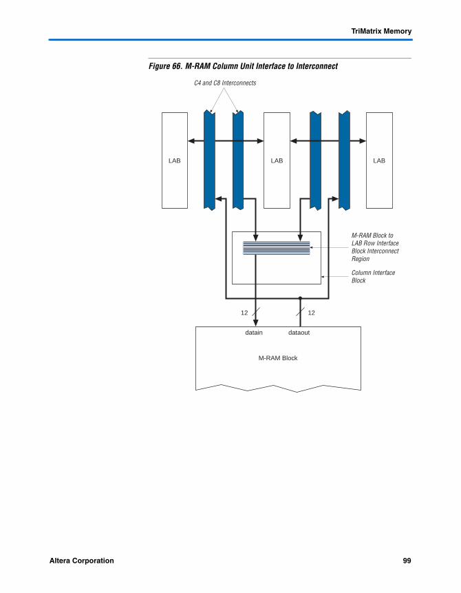
TriMatrix Memory
Figure 66. M-RAM Column Unit Interface to Interconnect
12 12
Column InterfaceBlock
M-RAM Block toLAB Row InterfaceBlock InterconnectRegion
datain dataout
LAB LABLAB
C4 and C8 Interconnects
M-RAM Block
Altera Corporation 99Preliminary
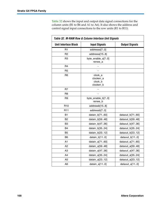
Stratix GX FPGA Family
Table 32 shows the input and output data signal connections for the column units (B1 to B6 and A1 to A6). It also shows the address and control signal input connections to the row units (R1 to R11).
Table 32. M-RAM Row & Column Interface Unit Signals
Unit Interface Block Input SIgnals Output Signals
R1 addressa[7..0]
R2 addressa[15..8]
R3 byte_enable_a[7..0]renwe_a
R4 -
R5 -
R6 clock_aclocken_aclock_b
clocken_b
R7 -
R8 -
R9 byte_enable_b[7..0]renwe_b
R10 addressb[15..8]
R11 addressb[7..0]
B1 datain_b[71..60] dataout_b[71..60]
B2 datain_b[59..48] dataout_b[59..48]
B3 datain_b[47..36] dataout_b[47..36]
B4 datain_b[35..24] dataout_b[35..24]
B5 datain_b[23..12] dataout_b[23..12]
B6 datain_b[11..0] dataout_b[11..0]
A1 datain_a[71..60] dataout_a[71..60]
A2 datain_a[59..48] dataout_a[59..48]
A3 datain_a[47..36] dataout_a[47..36]
A4 datain_a[35..24] dataout_a[35..24]
A5 datain_a[23..12] dataout_a[23..12]
A6 datain_a[11..0] dataout_a[11..0]
100 Altera CorporationPreliminary

TriMatrix Memory
Independent Clock Mode
The memory blocks implement independent clock mode for true dual-port memory. In this mode, a separate clock is available for each port (ports A and B). Clock A controls all registers on the port A side, while clock B controls all registers on the port B side. Each port, A and B, also supports independent clock enables and asynchronous clear signals for port A and B registers. Figure 67 shows a TriMatrix memory block in independent clock mode.
Altera Corporation 101Preliminary

Stratix GX FPGA Family
Figure 67. Independent Clock Mode Note (1)
Note to Figure 67:(1) All registers shown have asynchronous clear ports.
8D E
NA
Q
D EN
A
Q
D EN
A
Q
data
A[ ]
addr
ess A
[ ]
Mem
ory
Blo
ck25
6 ´
16 (
2)51
2 ´
81,
024
´ 4
2,04
8 ´
24,
096
´ 1
Dat
a In
Add
ress
A
Writ
e/R
ead
Ena
ble
Dat
a O
ut
Dat
a In
Add
ress
B
Writ
e/R
ead
Ena
ble
Dat
a O
ut
clke
n A
cloc
k A
D EN
A
Q
wre
n A
8 LA
B R
ow C
lock
s
q A[ ]
8da
taB[ ]
addr
ess B
[ ]
clke
n B
cloc
k B
wre
n B
q B[ ]
EN
A
AB
EN
ADQ
D EN
A
Qby
teen
a A[ ]
Byt
e E
nabl
e A
Byt
e E
nabl
e B
byte
ena B
[ ]
EN
ADQ
EN
ADQ
EN
ADQ
DQ
Writ
eP
ulse
Gen
erat
or
Writ
eP
ulse
Gen
erat
or
102 Altera CorporationPreliminary

TriMatrix Memory
Input/Output Clock Mode
Input/output clock mode can be implemented for both the true and simple dual-port memory modes. On each of the two ports, A or B, one clock controls all registers for inputs into the memory block: data input, wren, and address. The other clock controls the block’s data output registers. Each memory block port, A or B, also supports independent clock enables and asynchronous clear signals for input and output registers. Figures 68 and 69 show the memory block in input/output clock mode.
Altera Corporation 103Preliminary

Stratix GX FPGA Family
Figure 68. Input/Output Clock Mode in True Dual-Port Mode Note (1)
Note to Figure 68:(1) All registers shown have asynchronous clear ports.
8
D EN
A
Q
D EN
A
Q
D EN
A
Q
data
A[ ]
addr
ess A
[ ]
Mem
ory
Blo
ck25
6 ×
16 (2
)51
2 ×
81,
024
× 4
2,04
8 ×
24,
096
× 1
Dat
a In
Add
ress
A
Writ
e/R
ead
Ena
ble
Dat
a O
ut
Dat
a In
Add
ress
B
Writ
e/R
ead
Ena
ble
Dat
a O
ut
clke
n A
cloc
k A
D EN
A
Q
wre
n A
8 LA
B R
ow C
lock
s
q A[ ]
8
data
B[ ]
addr
ess B
[ ]
clke
n B
cloc
k B
wre
n B
q B[ ]
EN
A
AB
EN
ADQ
EN
ADQ
EN
ADQ
DQ
D EN
A
Qby
teen
a A[ ]
Byt
e E
nabl
e A
Byt
e E
nabl
e B
byte
ena B
[ ]
EN
ADQ
Writ
eP
ulse
Gen
erat
or
Writ
eP
ulse
Gen
erat
or
104 Altera CorporationPreliminary

TriMatrix Memory
Figure 69. Input/Output Clock Mode in Simple Dual-Port Mode Note (1)
Note to Figure 69:(1) All registers shown except the rden register have asynchronous clear ports.
Read/Write Clock Mode
The memory blocks implement read/write clock mode for simple dual-port memory. The designer can use up to two clocks in this mode. The write clock controls the block’s data inputs, wraddress, and wren. The read clock controls the data output, rdaddress, and rden. The memory blocks support independent clock enables for each clock and asynchronous clear signals for the read- and write-side registers. Figure 70 shows a memory block in read/write clock mode.
8
DENA
Q
D
ENA
Q
D
ENA
Q
D
ENA
Q
DENA
Q
data[ ]
DENA
Qwraddress[ ]
address[ ]
Memory Block256 ´ 16
512 ´ 81,024 ´ 42,048 ´ 24,096 ´ 1
Data In
Read Address
Write Address
Write Enable
Read Enable
Data Out
outclken
inclken
wrclock
rdclock
wren
rden
8 LAB Row Clocks
To MultiTrackInterconnect
DENA
Qbyteena[ ] Byte Enable
WritePulse
Generator
Altera Corporation 105Preliminary

Stratix GX FPGA Family
Figure 70. Read/Write Clock Mode in Simple Dual-Port Mode Note (1)
Note to Figure 70:(1) All registers shown except the rden register have asynchronous clear ports.
Single-Port Mode
The memory blocks also support single-port mode, used when simultaneous reads and writes are not required. See Figure 71. A single block in a memory block can support up to two single-port mode RAM blocks in the M4K RAM blocks if each RAM block is less than or equal to 2K bits in size.
8
DENA
Q
D
ENA
Q
D
ENA
Q
D
ENA
Q
DENA
Q
data[ ]
DENA
Qwraddress[ ]
address[ ]
Memory Block256 × 16
512 × 81,024 × 42,048 × 24,096 × 1
Data In
Read Address
Write Address
Write Enable
Read Enable
Data Out
outclken
inclken
wrclock
rdclock
wren
rden
8 LAB RowClocks
To MultiTrackInterconnect
DENA
Qbyteena[ ] Byte Enable
WritePulse
Generator
106 Altera CorporationPreliminary

Digital Signal Processing Block
Figure 71. Single-Port Mode
Digital Signal Processing Block
The most commonly used DSP functions are finite impulse response (FIR) filters, complex FIR filters, infinite impulse response (IIR) filters, fast Fourier transform (FFT) functions, direct cosine transform (DCT) functions, and correlators. All of these blocks have the same fundamental building block: the multiplier. Additionally, some applications need specialized operations such as multiply-add and multiply-accumulate operations. Stratix GX devices provide DSP blocks to meet the arithmetic requirements of these functions.
Each Stratix GX device has two columns of DSP blocks to efficiently implement DSP functions faster than LE-based implementations. Larger Stratix GX devices have more DSP blocks per column (see Table 33). Each DSP block can be configured to support up to:
Eight 9 × 9-bit multipliers Four 18 × 18-bit multipliers One 36 × 36-bit multiplier
As indicated, the Stratix GX DSP block can support one 36 × 36-bit multiplier in a single DSP block. This is true for any matched sign multiplications (either unsigned by unsigned or signed by signed), but
8
DENA
Q
D
ENA
Q
D
ENA
Q
DENA
Q
data[ ]
address[ ]
RAM/ROM256 × 16
512 × 81,024 × 42,048 × 24,096 × 1
Data In
Address
Write Enable
Data Out
outclken
inclken
inclock
outclock
WritePulse
Generator
wren
8 LAB RowClocks
To MultiTrackInterconnect
Altera Corporation 107Preliminary

Stratix GX FPGA Family
the capabilities for dynamic and mixed sign multiplications are handled differently. The following list provides the largest functions that can fit into a single DSP block.
36 × 36-bit unsigned by unsigned multiplication 36 × 36-bit signed by signed multiplication 35 × 36-bit unsigned by signed multiplication 36 × 35-bit signed by unsigned multiplication 36 × 35-bit signed by dynamic sign multiplication 35 × 36-bit dynamic sign by signed multiplication 35 × 36-bit unsigned by dynamic sign multiplication 36 × 35-bit dynamic sign by unsigned multiplication 35 × 35-bit dynamic sign multiplication when the sign controls for
each operand are different 36 × 36-bit dynamic sign multiplication when the same sign control
is used for both operands
1 This list only shows functions that can fit into a single DSP block. Multiple DSP blocks can support larger multiplication functions.
Figure 72 shows one of the columns with surrounding LAB rows.
108 Altera CorporationPreliminary
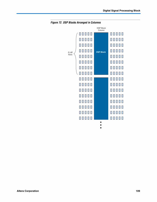
Digital Signal Processing Block
Figure 72. DSP Blocks Arranged in Columns
DSP BlockColumn
8 LABRows
DSP Block
Altera Corporation 109Preliminary

Stratix GX FPGA Family
Table 33 shows the number of DSP blocks in each Stratix GX device.
DSP block multipliers can optionally feed an adder/subtractor or accumulator within the block depending on the configuration. This makes routing to LEs easier, saves LE routing resources, and increases performance, because all connections and blocks are within the DSP block. Additionally, the DSP block input registers can efficiently implement shift registers for FIR filter applications.
Figure 73 shows the top-level diagram of the DSP block configured for 18 × 18-bit multiplier mode. Figure 74 shows the 9 × 9-bit multiplier configuration of the DSP block.
Table 33. DSP Blocks in Stratix GX Devices Notes (1), (2)
Device DSP Blocks Total 9 × 9 Multipliers
Total 18 × 18 Multipliers
Total 36 × 36 Multipliers
EP1SGX10 6 48 24 6
EP1SGX25 10 80 40 10
EP1SGX40 14 112 56 14
Notes to Table 33:(1) Each device has either the number of 9 × 9-, 18 × 18-, or 36 × 36-bit multipliers
shown. The total number of multipliers for each device is not the sum of all the multipliers.
(2) The number of supported multiply functions shown is based on signed/signed or unsigned/unsigned implementations.
110 Altera CorporationPreliminary

Digital Signal Processing Block
Figure 73. DSP Block Diagram for 18 × 18-Bit Configuration
Adder/Subtractor/
Accumulator2
Adder/Subtractor/
Accumulator1
Summation
Optional PipelineRegister Stage
Multiplier Stage
Output SelectionMultiplexer
Optional Output Register Stage
CLRN
D Q
ENA
CLRN
D Q
ENA
CLRN
D Q
ENA
CLRN
D Q
ENA
CLRN
D Q
ENA
CLRN
D Q
ENA
CLRN
D Q
ENA
CLRN
D Q
ENA
CLRN
D Q
ENA
CLRN
D Q
ENA
CLRN
D Q
ENA
CLRN
D Q
ENA
Optional Serial Shift RegisterInputs from Previous DSP Block
Optional Stage Configurableas Accumulator or DynamicAdder/Subtractor
Summation Stagefor Adding FourMultipliers Together
Optional Input RegisterStage with Parallel Input orShift Register Configuration
Optional Serial Shift Register Outputs to Next DSP Blockin the Column
to MultiTrackInterconnect
Altera Corporation 111Preliminary

Stratix GX FPGA Family
Figure 74. DSP Block Diagram for 9 × 9-Bit Configuration
CLRN
D QENA
CLRN
D QENA
CLRN
D QENA
Adder/Subtractor/
1a
Summation
Summation
CLRN
D QENA
CLRN
D QENA
CLRN
D QENA
CLRN
D QENA
CLRN
D QENA
CLRN
D QENA
CLRN
D QENA
Adder/Subtractor/
1b
CLRN
D QENA
CLRN
D QENA
CLRN
D QENA
CLRN
D QENA
CLRN
D QENA
CLRN
D QENA
Adder/Subtractor/
2a
CLRN
D QENA
CLRN
D QENA
CLRN
D QENA
CLRN
D QENA
CLRN
D QENA
CLRN
D QENA
Adder/Subtractor/
2b
CLRN
D QENA
CLRN
D QENA
CLRN
D QENA
OutputSelection
Multiplexer
To MultiTrackInterconnect
112 Altera CorporationPreliminary
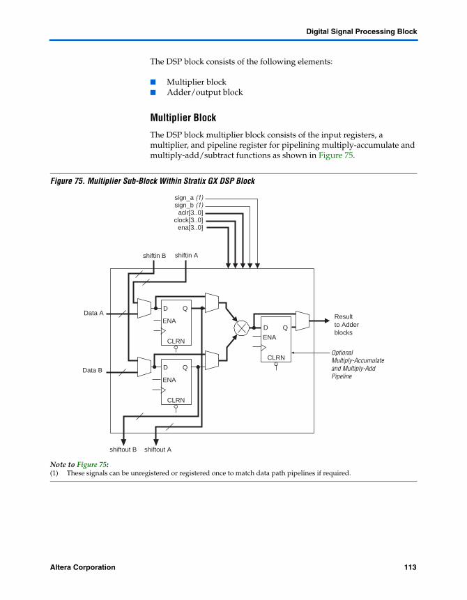
Digital Signal Processing Block
The DSP block consists of the following elements:
Multiplier block Adder/output block
Multiplier Block
The DSP block multiplier block consists of the input registers, a multiplier, and pipeline register for pipelining multiply-accumulate and multiply-add/subtract functions as shown in Figure 75.
Figure 75. Multiplier Sub-Block Within Stratix GX DSP Block
Note to Figure 75:(1) These signals can be unregistered or registered once to match data path pipelines if required.
CLRN
D Q
ENA
Data A
Data B
Resultto Adderblocks
shiftout B shiftout A
shiftin Ashiftin B
aclr[3..0]clock[3..0]
ena[3..0]
OptionalMultiply-Accumulateand Multiply-AddPipeline
sign_a (1)sign_b (1)
CLRN
D Q
ENA
CLRN
D Q
ENA
Altera Corporation 113Preliminary

Stratix GX FPGA Family
Input Registers
A bank of optional input registers is located at the input of each multiplier and multiplicand inputs to the multiplier. When these registers are configured for parallel data inputs, they are driven by regular routing resources. Designers can use a clock signal, asynchronous clear signal, and a clock enable signal to independently control each set of A and B inputs for each multiplier in the DSP block. Designers select these control signals from a set of four different clock[3..0], aclr[3..0], and ena[3..0] signals that drive the entire DSP block.
Designers can also configure the input registers for a shift register application. In this case, the input registers feed the multiplier and drive two dedicated shift output lines: shiftoutA and shiftoutB. The shift outputs of one multiplier block directly feed the adjacent multiplier block in the same DSP block (or the next DSP block) as shown in Figure 76, to form a shift register chain. This chain can terminate in any block, i.e., designers can create any length of shift register chain up to 224 registers. The designer can use the input shift registers for FIR filter applications. One set of shift inputs can provide data for a filter, and the other are coefficients that are optionally loaded in serial or parallel. When implementing 9 × 9- and 18 × 18-bit multipliers, the designer does not need to implement external shift registers in LAB LEs. The designer implements all the filter circuitry within the DSP block and its routing resources, saving LE and general routing resources for general logic. External registers are needed for shift register inputs when using 36 × 36-bit multipliers.
114 Altera CorporationPreliminary

Digital Signal Processing Block
Figure 76. Multiplier Sub-Blocks Using Input Shift Register Connections Note (1)
Note to Figure 76:(1) Either Data A or Data B input can be set to a parallel input for constant coefficient multiplication.
CLRN
D Q
ENA
Data A
Data B
A[n] × B[n]
CLRN
D Q
ENA
CLRN
D Q
ENA
CLRN
D Q
ENA
Data AData B
A[n Ð 1] × B[n Ð 1]
CLRN
D Q
ENA
CLRN
D Q
ENA
CLRN
D Q
ENA
Data AData B
A[n Ð 2] × B[n Ð 2]
CLRN
D Q
ENA
CLRN
D Q
ENA
Altera Corporation 115Preliminary
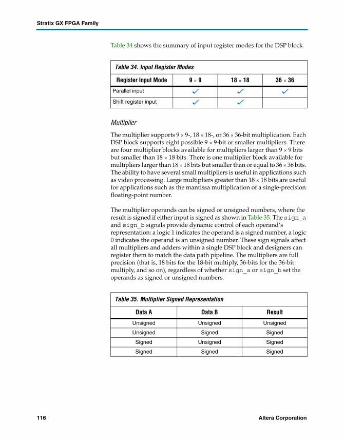
Stratix GX FPGA Family
Table 34 shows the summary of input register modes for the DSP block.
Multiplier
The multiplier supports 9 × 9-, 18 × 18-, or 36 × 36-bit multiplication. Each DSP block supports eight possible 9 × 9-bit or smaller multipliers. There are four multiplier blocks available for multipliers larger than 9 × 9 bits but smaller than 18 × 18 bits. There is one multiplier block available for multipliers larger than 18 × 18 bits but smaller than or equal to 36 × 36 bits. The ability to have several small multipliers is useful in applications such as video processing. Large multipliers greater than 18 × 18 bits are useful for applications such as the mantissa multiplication of a single-precision floating-point number.
The multiplier operands can be signed or unsigned numbers, where the result is signed if either input is signed as shown in Table 35. The sign_a and sign_b signals provide dynamic control of each operand’s representation: a logic 1 indicates the operand is a signed number, a logic 0 indicates the operand is an unsigned number. These sign signals affect all multipliers and adders within a single DSP block and designers can register them to match the data path pipeline. The multipliers are full precision (that is, 18 bits for the 18-bit multiply, 36-bits for the 36-bit multiply, and so on), regardless of whether sign_a or sign_b set the operands as signed or unsigned numbers.
Table 34. Input Register Modes
Register Input Mode 9 × 9 18 × 18 36 × 36
Parallel input v v v
Shift register input v v
Table 35. Multiplier Signed Representation
Data A Data B Result
Unsigned Unsigned Unsigned
Unsigned Signed Signed
Signed Unsigned Signed
Signed Signed Signed
116 Altera CorporationPreliminary
Digital Signal Processing Block
Pipeline/Post Multiply Register
The output of 9 × 9- or 18 × 18-bit multipliers can optionally feed a register to pipeline multiply-accumulate and multiply-add/subtract functions. For 36 × 36-bit multipliers, this register will pipeline the multiplier function.
Adder/Output Blocks
The result of the multiplier sub-blocks are sent to the adder/output block which consist of an adder/subtractor/accumulator unit, summation unit, output select multiplexer, and output registers. The results are used to configure the adder/output block as a pure output, accumulator, a simple two-multiplier adder, four-multiplier adder, or final stage of the 36-bit multiplier. The designer can configure the adder/output block to use output registers in any mode, and must use output registers for the accumulator. The system cannot use adder/output blocks independently of the multiplier. Figure 77 shows the adder and output stages.
Altera Corporation 117Preliminary
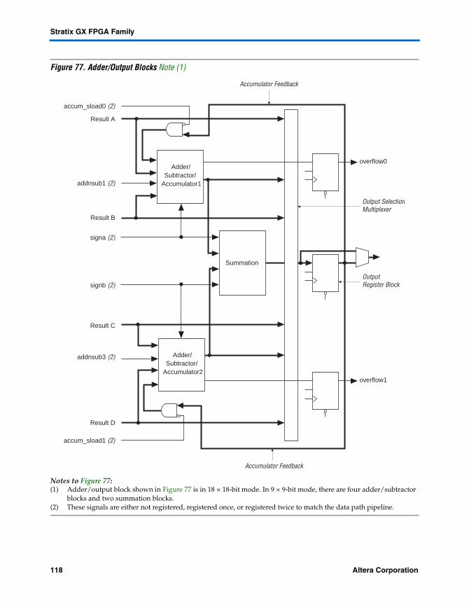
Stratix GX FPGA Family
Figure 77. Adder/Output Blocks Note (1)
Notes to Figure 77:(1) Adder/output block shown in Figure 77 is in 18 × 18-bit mode. In 9 × 9-bit mode, there are four adder/subtractor
blocks and two summation blocks.(2) These signals are either not registered, registered once, or registered twice to match the data path pipeline.
Adder/Subtractor/
Accumulator1
Summation
Result A
Result B
Result C
Result D
addnsub1 (2)
accum_sload0 (2)
addnsub3 (2)
signa (2)
signb (2)
accum_sload1 (2)
Accumulator Feedback
Accumulator Feedback
overflow0
Adder/Subtractor/
Accumulator2
Output SelectionMultiplexer
Output Register Block
overflow1
118 Altera CorporationPreliminary
Digital Signal Processing Block
Adder/Subtractor/Accumulator
The adder/subtractor/accumulator is the first level of the adder/output block and can be used as an accumulator or as an adder/subtractor.
Adder/SubtractorEach adder/subtractor/accumulator block can perform addition or subtraction using the addnsub independent control signal for each first-level adder in 18 × 18-bit mode. There are two addnsub[1..0] signals available in a DSP block for any configuration. For 9 × 9-bit mode, one addnsub[1..0] signal controls the top two one-level adders and another addnsub[1..0] signal controls the bottom two one-level adders. A high addnsub signal indicates addition, and a low signal indicates subtraction. The addnsub control signal can be unregistered or registered once or twice when feeding the adder blocks to match data path pipelines.
The signa and signb signals serve the same function as the multiplier block signa and signb signals. The only difference is that these signals can be registered up to two times. These signals are tied to the same signa and signb signals from the multiplier and must be connected to the same clocks and control signals.
AccumulatorWhen configured for accumulation, the adder/output block output feeds back to the accumulator as shown in Figure 77. The accum_sload[1..0] signal synchronously loads the multiplier result to the accumulator output. This signal can be unregistered or registered once or twice. Additionally, the overflow signal indicates the accumulator has overflowed or underflowed in accumulation mode. This signal is always registered and must be externally latched in LEs if the design requires a latched overflow signal.
Summation
The output of the adder/subtractor/accumulator block feeds to an optional summation block. This block sums the outputs of the DSP block multipliers. In 9 × 9-bit mode, there are two summation blocks providing the sums of two sets of four 9 × 9-bit multipliers. In 18 × 18-bit mode, there is one summation providing the sum of one set of four 18 × 18-bit multipliers.
Altera Corporation 119Preliminary

Stratix GX FPGA Family
Output Selection Multiplexer
The outputs from the various elements of the adder/output block are routed through an output selection multiplexer. Based on the DSP block operational mode and user settings, the multiplexer selects whether the output from the multiplier, the adder/subtractor/accumulator, or summation block feeds to the output.
Output Registers
Optional output registers for the DSP block outputs are controlled by four sets of control signals: clock[3..0], aclr[3..0], and ena[3..0]. Output registers can be used in any mode.
Modes of Operation
The adder, subtractor, and accumulate functions of a DSP block have four modes of operation:
Simple multiplier Multiply-accumulator Two-multipliers adder Four-multipliers adder
1 Each DSP block can only support one mode. Mixed modes in the same DSP block is not supported.
Simple Multiplier Mode
In simple multiplier mode, the DSP block drives the multiplier sub-block result directly to the output with or without an output register. Up to four 18 × 18-bit multipliers or eight 9 × 9-bit multipliers can drive their results directly out of one DSP block. See Figure 78.
120 Altera CorporationPreliminary

Digital Signal Processing Block
Figure 78. Simple Multiplier Mode
Note to Figure 78:(1) These signals are not registered or registered once to match the data path pipeline.
DSP blocks can also implement one 36 × 36-bit multiplier in multiplier mode. DSP blocks use four 18 × 18-bit multipliers combined with dedicated adder and internal shift circuitry to achieve 36-bit multiplication. The input shift register feature is not available for the 36 × 36-bit multiplier. In 36 × 36-bit mode, the device can use the register that is normally a multiplier-result-output register as a pipeline stage for the 36 × 36-bit multiplier. Figure 79 shows the 36 × 36-bit multiply mode.
CLRN
D Q
ENA
Data A
Data B
Data Out
shiftout B shiftout A
shiftin Ashiftin B
aclrclock
ena
signa (1)signb (1)
CLRN
D Q
ENA
CLRN
D Q
ENA
CLRN
D Q
ENA
Altera Corporation 121Preliminary

Stratix GX FPGA Family
Figure 79. 36 × 36 Multiply Mode
Notes to Figure 79:(1) These signals are not registered or registered once to match the pipeline.(2) These signals are not registered, registered once, or registered twice for latency to match the pipeline.
CLRN
D Q
ENA
A[17..0]
A[17..0]
B[17..0]
B[17..0]
A[35..18]
A[35..18]
B[35..18]
B[35..18]
aclrclock
ena
signa (1)signb (1)
CLRN
D Q
ENA
CLRN
D Q
ENA
CLRN
D Q
ENA
CLRN
D Q
ENA
CLRN
D Q
ENA
CLRN
D Q
ENA
CLRN
D Q
ENA
CLRN
D Q
ENA
CLRN
D Q
ENA
CLRN
D Q
ENA
CLRN
D Q
ENA
CLRN
D Q
ENA
Data Out
36 × 36Multiplier
Adder
signa (2)
signb (2)
122 Altera CorporationPreliminary

Digital Signal Processing Block
Multiply-Accumulator Mode
In multiply-accumulator mode (see Figure 80), the DSP block drives multiplied results to the adder/subtractor/accumulator block configured as an accumulator. A designer can implement one or two multiply-accumulators up to 18 × 18 bits in one DSP block. The first and third multiplier sub-blocks are unused in this mode, since only one multiplier can feed one of two accumulators. The multiply-accumulator output can be up to 52 bits—a maximum of a 36-bit result with 16 bits of accumulation. The accum_sload and overflow signals are only available in this mode. The addnsub signal can set the accumulator for decimation and the overflow signal will indicate underflow condition.
Figure 80. Multiply-Accumulate Mode
Notes to Figure 80:(1) These signals are not registered or registered once to match the data path pipeline.(2) These signals are not registered, registered once, or registered twice for latency to match the data path pipeline.
Two-Multipliers Adder Mode
The two-multipliers adder mode uses the adder/subtractor/accumulator block to add or subtract the outputs of the multiplier block, which is useful for applications such as FFT functions and complex FIR filters. A single DSP block can implement two sums or differences from two 18 × 18-bit multipliers each or four sums or differences from two 9 × 9-bit multipliers each.
CLRN
D Q
ENA
CLRN
D Q
ENA
Data A
Data B
Data Out
overflow
Shiftout B Shiftout A
Shiftin AShiftin B
aclrclock
ena
signa (1)signb (1)
CLRN
D Q
ENA
CLRN
D Q
ENA
Accumulator
addnsub (2)signa (2)signb (2)
accum_sload (2)
Altera Corporation 123Preliminary

Stratix GX FPGA Family
Designers can use the two-multipliers adder mode for complex multiplications, which are written as:
(a + jb) × (c + jd) = [(a × c) – (b × d)] + j × [(a × d) + (b × c)]
The two-multipliers adder mode allows a single DSP block to calculate the real part [(a × c) – (b × d)] using one subtractor and the imaginary part [(a × d) + (b × c)] using one adder, for data widths up to 18 bits. Two complex multiplications are possible for data widths up to 9 bits using four adder/subtractor/accumulator blocks. Figure 81 shows an 18-bit two-multipliers adder.
Figure 81. Two-Multipliers Adder Mode Implementing Complex Multiply
Four-Multipliers Adder Mode
In the four-multipliers adder mode, the DSP block adds the results of two first -stage adder/subtractor blocks. One sum of four 18 × 18-bit multipliers or two different sums of two sets of four 9 × 9-bit multipliers can be implemented in a single DSP block. The product width for each multiplier must be the same size. The four-multipliers adder mode is useful for FIR filter applications. Figure 82 shows the four multipliers adder mode.
Subtractor
36
36
18
18
18
37
A18
(A × C) − (B × D)(Real Part)
Adder
36
36
18
18
37
A
18
18
18
(A × D) + (B × C)(Imaginary Part)
18
18
18
DSP Block
C
B
D
D
B
C
124 Altera CorporationPreliminary
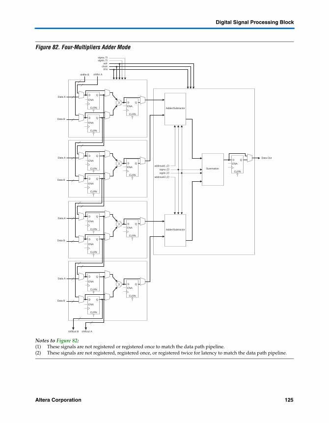
Digital Signal Processing Block
Figure 82. Four-Multipliers Adder Mode
Notes to Figure 82:(1) These signals are not registered or registered once to match the data path pipeline.(2) These signals are not registered, registered once, or registered twice for latency to match the data path pipeline.
CLRN
D Q
ENA
Data A
Data B
shiftin Ashiftin B
aclrclock
ena
signa (1)signb (1)
CLRN
D Q
ENA
CLRN
D Q
ENA
CLRN
D Q
ENA
Data A
Data B
CLRN
D Q
ENA
CLRN
D Q
ENA
Adder/Subtractor
CLRN
D Q
ENA
Data A
Data B
CLRN
D Q
ENA
CLRN
D Q
ENA
CLRN
D Q
ENA
Data A
Data B
shiftout B shiftout A
CLRN
D Q
ENA
CLRN
D Q
ENA
Adder/Subtractor
addnsub1 (2)signa (2)signb (2) CLRN
D Q
ENA
Data Out
addnsub3 (2)
Summation
Altera Corporation 125Preliminary
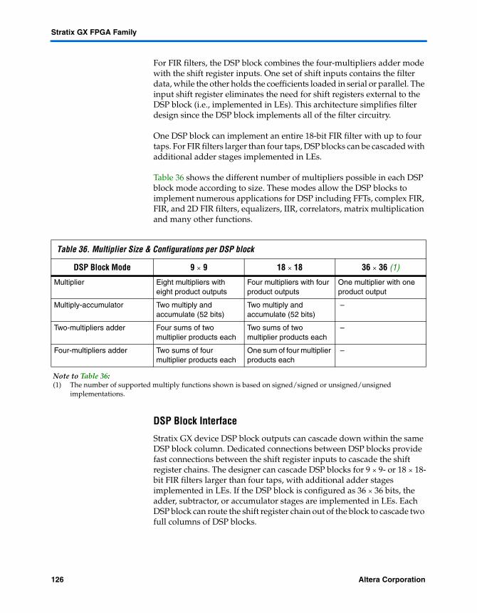
Stratix GX FPGA Family
For FIR filters, the DSP block combines the four-multipliers adder mode with the shift register inputs. One set of shift inputs contains the filter data, while the other holds the coefficients loaded in serial or parallel. The input shift register eliminates the need for shift registers external to the DSP block (i.e., implemented in LEs). This architecture simplifies filter design since the DSP block implements all of the filter circuitry.
One DSP block can implement an entire 18-bit FIR filter with up to four taps. For FIR filters larger than four taps, DSP blocks can be cascaded with additional adder stages implemented in LEs.
Table 36 shows the different number of multipliers possible in each DSP block mode according to size. These modes allow the DSP blocks to implement numerous applications for DSP including FFTs, complex FIR, FIR, and 2D FIR filters, equalizers, IIR, correlators, matrix multiplication and many other functions.
DSP Block Interface
Stratix GX device DSP block outputs can cascade down within the same DSP block column. Dedicated connections between DSP blocks provide fast connections between the shift register inputs to cascade the shift register chains. The designer can cascade DSP blocks for 9 × 9- or 18 × 18-bit FIR filters larger than four taps, with additional adder stages implemented in LEs. If the DSP block is configured as 36 × 36 bits, the adder, subtractor, or accumulator stages are implemented in LEs. Each DSP block can route the shift register chain out of the block to cascade two full columns of DSP blocks.
Table 36. Multiplier Size & Configurations per DSP block
DSP Block Mode 9 × 9 18 × 18 36 × 36 (1)
Multiplier Eight multipliers with eight product outputs
Four multipliers with four product outputs
One multiplier with one product output
Multiply-accumulator Two multiply and accumulate (52 bits)
Two multiply and accumulate (52 bits)
–
Two-multipliers adder Four sums of two multiplier products each
Two sums of two multiplier products each
–
Four-multipliers adder Two sums of four multiplier products each
One sum of four multiplier products each
–
Note to Table 36:(1) The number of supported multiply functions shown is based on signed/signed or unsigned/unsigned
implementations.
126 Altera CorporationPreliminary
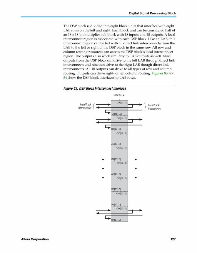
Digital Signal Processing Block
The DSP block is divided into eight block units that interface with eight LAB rows on the left and right. Each block unit can be considered half of an 18 × 18-bit multiplier sub-block with 18 inputs and 18 outputs. A local interconnect region is associated with each DSP block. Like an LAB, this interconnect region can be fed with 10 direct link interconnects from the LAB to the left or right of the DSP block in the same row. All row and column routing resources can access the DSP block’s local interconnect region. The outputs also work similarly to LAB outputs as well. Nine outputs from the DSP block can drive to the left LAB through direct link interconnects and nine can drive to the right LAB though direct link interconnects. All 18 outputs can drive to all types of row and column routing. Outputs can drive right- or left-column routing. Figures 83 and 84 show the DSP block interfaces to LAB rows.
Figure 83. DSP Block Interconnect Interface
A1[17..0]
B1[17..0]
A2[17..0]
B2[17..0]
A3[17..0]
B3[17..0]
A4[17..0]
B4[17..0]
OA[17..0]
OB[17..0]
OC[17..0]
OD[17..0]
OE[17..0]
OF[17..0]
OG[17..0]
OH[17..0]
DSP Block
MultiTrackInterconnect
MultiTrackInterconnect
Altera Corporation 127Preliminary

Stratix GX FPGA Family
Figure 84. DSP Block Interface to Interconnect
A bus of 18 control signals feeds the entire DSP block. These signals include clock[0..3] clocks, aclr[0..3] asynchronous clears, ena[1..4] clock enables, signa, signb signed/unsigned control signals, addnsub1 and addnsub3 addition and subtraction control signals, and accum_sload[0..1] accumulator synchronous loads. The
LAB LAB
Row InterfaceBlock
DSP BlockRow Structure
10
[17..0][17..0]
DSP Block toLAB Row InterfaceBlock Interconnect Region
18 Inputs per Row 18 Outputs per Row
R4 and R8 Interconnects
C4 and C8 Interconnects
Direct Link Interconnectfrom Adjacent LAB
Nine Direct Link Outputsto Adjacent LABs
Direct Link Interconnectfrom Adjacent LAB
18
18
18
Control3
9 9
10
128 Altera CorporationPreliminary

PLLs & Clock Networks
clock signals are routed from LAB row clocks and are generated from specific LAB rows at the DSP block interface. The LAB row source for control signals, data inputs, and outputs is shown in Table 37.
PLLs & Clock Networks
Stratix GX devices provide a hierarchical clock structure and multiple PLLs with advanced features. The large number of clocking resources in combination with the clock synthesis precision provided by enhanced and fast PLLs provides a complete clock management solution. Stratix GX devices contain up to four enhanced PLLs and up to four fast PLLs. In addition, there are four receiver PLLs and one transmitter PLL per transceiver block located on the right side of Stratix GX devices.
Global & Hierarchical Clocking
Stratix GX devices provide 16 dedicated global clock networks, 16 regional clock networks (four per device quadrant), 8 dedicated fast regional clock networks within EP1SGX10 and EP1SGX25, and 16 dedicated fast regional clock networks within EP1SGX40 devices.
Table 37. DSP Block Signal Sources & Destinations
LAB Row at Interface
Control Signals Generated Data Inputs Data Outputs
1 signa A1[17..0] OA[17..0]
2 aclr0accum_sload0
B1[17..0] OB[17..0]
3 addnsub1clock0ena0
A2[17..0] OC[17..0]
4 aclr1clock1ena1
B2[17..0] OD[17..0]
5 aclr2clock2ena2
A3[17..0] OE[17..0]
6 sign_bclock3ena3
B3[17..0] OF[17..0]
7 clear3accum_sload1
A4[17..0] OG[17..0]
8 addnsub3 B4[17..0] OH[17..0]
Altera Corporation 129Preliminary

Stratix GX FPGA Family
These clocks are organized into a hierarchical clock structure that allows for up to 22 clocks per device region with low skew and delay. This hierarchical clocking scheme provides up to 40 unique clock domains within EP1SGX10 and EP1SGX25 devices, and 48 unique clock domains within EP1SGX40 devices.
There are 12 dedicated clock pins (CLK[15..12], and CLK[7..0]) to drive either the global or regional clock networks. Three clock pins drive the top, bottom, and left side of the device. Enhanced and fast PLL outputs as well as an I/O interface can also drive these global and regional clock networks.
There are up to 20 recovered clocks (rxclkout[20..0]) and up to 5 transmitter clock outputs (coreclk_out) which can drive any of the global clock networks (CLK[15..0]), as shown in Figure 85.
Global Clock Network
These clocks drive throughout the entire device, feeding all device quadrants. The global clock networks can be used as clock sources for all resources within the device IOEs, LEs, DSP blocks, and all memory blocks. These resources can also be used for control signals, such as clock enables and synchronous or asynchronous clears fed from the external pin. The global clock networks can also be driven by internal logic for internally generated global clocks and asynchronous clears, clock enables, or other control signals with large fanout. Figure 85 shows the 12 dedicated CLK pins and the transceiver clocks driving global clock networks.
130 Altera CorporationPreliminary
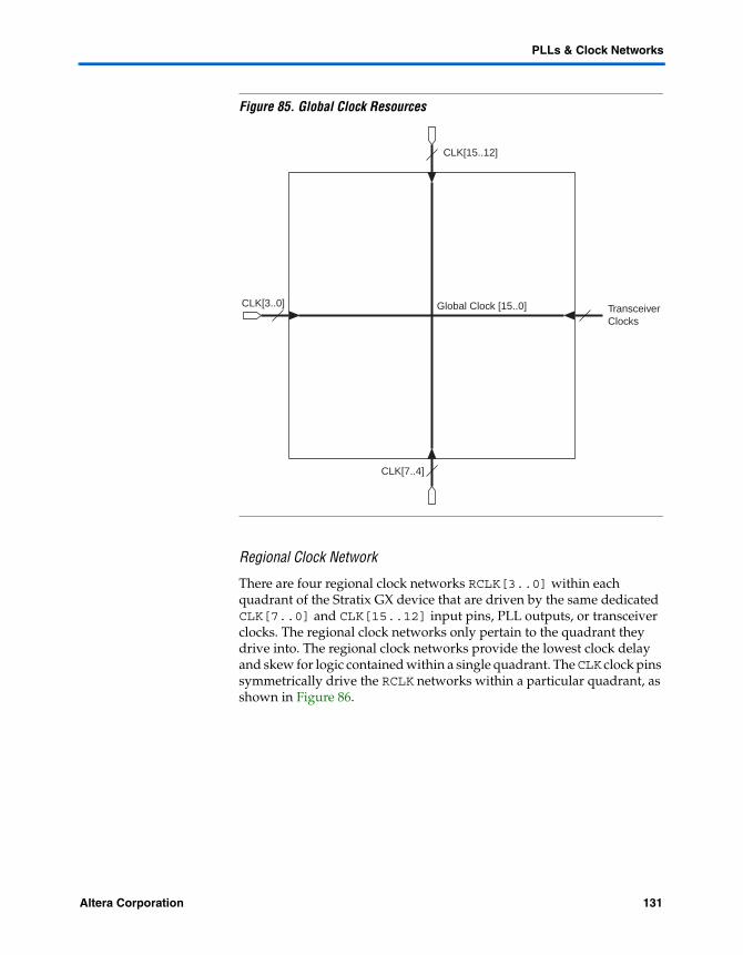
PLLs & Clock Networks
Figure 85. Global Clock Resources
Regional Clock Network
There are four regional clock networks RCLK[3..0] within each quadrant of the Stratix GX device that are driven by the same dedicated CLK[7..0] and CLK[15..12] input pins, PLL outputs, or transceiver clocks. The regional clock networks only pertain to the quadrant they drive into. The regional clock networks provide the lowest clock delay and skew for logic contained within a single quadrant. The CLK clock pins symmetrically drive the RCLK networks within a particular quadrant, as shown in Figure 86.
CLK[15..12]
CLK[3..0]
CLK[7..4]
Global Clock [15..0] TransceiverClocks
Altera Corporation 131Preliminary

Stratix GX FPGA Family
Figure 86. Regional Clocks
Fast Regional Clock Network
In EP1SGX25 and EP1SGX10 devices, there are two fast regional clock networks, FCLK[1..0], within each quadrant, fed by input pins (see Figure 87). In EP1SGX40 devices, there are two fast regional clock networks within each half-quadrant (see Figure 88). The FCLK[1..0] clocks can also be used for high fanout control signals, such as asynchronous clears, presets, clock enables, or protocol control signals such as TRDY and IRDY for PCI. Dual-purpose FCLK pins drive the fast clock networks. All devices have eight FCLK pins to drive fast regional clock networks. Any I/O pin can drive a clock or control signal onto any fast regional clock network with the addition of a delay. The I/O interconnect drives this signal.
RCLK[1..0]
RCLK[3..2]
RCLK[5..4] RCLK[7..6]
RCLK[15..14] RCLK[13..12]
RCLK[9..8]
RCLK[11..10]
CLK[15..12]
CLK[3..0]
CLK[7..4]
Regional Clocks Only Drive a Device Quadrant from Specified CLK Pins, Recovered Clocks, or PLLs within that Quadrant
TransceiverClocks
132 Altera CorporationPreliminary

PLLs & Clock Networks
Figure 87. EP1SGX25 & EP1SGX10 Device Fast Clock Pin Connections to Fast Regional Clocks
FCLK[1..0]
FCLK[1..0]
FCLK[1..0]
FCLK[1..0]
[3..2] [1..0]
[5..4] [7..6]
Fast Clock Fast Clock
Fast ClockFast Clock
Altera Corporation 133Preliminary

Stratix GX FPGA Family
Figure 88. EP1SGX40 Device Fast Regional Clock Pin Connections to Fast Regional Clocks
Combined Resources
Within each region, there are 22 distinct dedicated clocking resources consisting of 16 global clock lines, 4 regional clock lines, and 2 fast regional clock lines. Multiplexers are used with these clocks to form 8-bit busses to drive LAB row clocks, column IOE clocks, or row IOE clocks. Another multiplexer is used at the LAB level to select two of the eight row clocks to feed the LE registers within the LAB. See Figure 89.
[3]
Fast Clock
[2]
Fast Clock
[1]
Fast Clock
[0]
[4] [5] [6] [7]
Fast Clock
fclk[1..0]
Fast ClockFast Clock Fast ClockFast Clock
134 Altera CorporationPreliminary
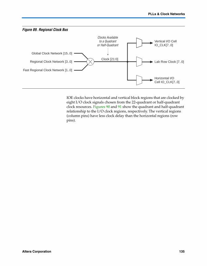
PLLs & Clock Networks
Figure 89. Regional Clock Bus
IOE clocks have horizontal and vertical block regions that are clocked by eight I/O clock signals chosen from the 22-quadrant or half-quadrant clock resources. Figures 90 and 91 show the quadrant and half-quadrant relationship to the I/O clock regions, respectively. The vertical regions (column pins) have less clock delay than the horizontal regions (row pins).
Clock [21:0]
Vertical I/O CellIO_CLK[7..0]
Lab Row Clock [7..0]
Horizontal I/OCell IO_CLK[7..0]
Global Clock Network [15..0]
Fast Regional Clock Network [1..0]
Regional Clock Network [3..0]
Clocks Availableto a Quadrant
or Half-Quadrant
Altera Corporation 135Preliminary

Stratix GX FPGA Family
Figure 90. EP1SGX25 & EP1SGX10 Device I/O Clock Groups
IO_CLKF[7:0] IO_CLKE[7:0]
IO_CLKA[7:0] IO_CLKB[7:0]
IO_CLKH[7:0]
IO_CLKG[7:0]
8
8
22 Clocks inthe Quadrant
22 Clocks inthe Quadrant
22 Clocks inthe Quadrant
22 Clocks inthe Quadrant
8
8
8 8I/O Clock Regions
13
14
16
15
136 Altera CorporationPreliminary

PLLs & Clock Networks
Figure 91. EP1SGX40 Device I/O Clock Groups
Designers can use the Quartus II software to control whether a clock input pin is either global, regional, or fast regional. The Quartus II software automatically selects the clocking resources if not specified.
Enhanced & Fast PLLs
Stratix GX devices provide robust clock management and synthesis using up to four enhanced PLLs and four fast PLLs. These PLLs increase performance and provide advanced clock interfacing and clock frequency synthesis. With features such as clock switchover, spread spectrum
IO_CLKJ[7:0] IO_CLKI[7:0]
IO_CLKA[7:0] IO_CLKB[7:0]
8
22 Clocks in theHalf-Quadrant
22 Clocks in theHalf-Quadrant
22 Clocks in theHalf-Quadrant
22 Clocks in theHalf-Quadrant
22 Clocks in theHalf-Quadrant
22 Clocks in theHalf-Quadrant
22 Clocks in theHalf-Quadrant
22 Clocks in theHalf-Quadrant
8 8 8
I/O Clock Regions
IO_CLKL[7:0] IO_CLKK[7:0]
IO_CLKC[7:0] IO_CLKD[7:0]
8 8 8 8
8
8
8
8
IO_CLKN[7:0]
IO_CLKM[7:0]
IO_CLKP[7:0]
IO_CLKO[7:0]
13
14
17
16
15
Altera Corporation 137Preliminary

Stratix GX FPGA Family
clocking, programmable bandwidth, phase and delay control, and dynamic PLL reconfiguration, the Stratix GX device’s enhanced PLLs provide designers with complete control of their clocks and system timing. The fast PLLs provide general purpose clocking with multiplication and phase shifting as well as high-speed outputs for high-speed differential I/O support. Enhanced and fast PLLs work together with the Stratix GX high-speed I/O and advanced clock architecture to provide significant improvements in system performance and bandwidth.
The Quartus II software enables the PLLs and their features without requiring any external devices. Table 38 shows which PLLs are available for each Stratix GX device and their type. Table 39 shows the enhanced PLL and fast PLL features in Stratix GX devices.
Table 38. Stratix GX Device PLL Availability
DeviceFast PLLs Enhanced PLLs
1 2 3 (1) 4 (1) 7 8 9 (1) 10 (1) 5 (2) 6 (2) 11 (3) 12 (3)
EP1SGX10 v v v v
EP1SGX25 v v v v
EP1SGX40 v v v v v v v v
Notes to Table 38:(1) PLLs 3, 4, 9, and 10 are not available in Stratix GX devices. However, these PLLs are listed in Table 38 because the
Stratix GX PLL numbering scheme is consistent with Stratix devices.(2) PLLs 5 and 6 each have eight single-ended outputs or four differential outputs.(3) PLLs 11 and 12 each have one single-ended output.
Table 39. Stratix GX Enhanced PLL & Fast PLL Features (Part 1 of 2) Notes (1)–(8)
Feature Enhanced PLL Fast PLL
Clock multiplication and division m/ (n × post-scale counter) (1) m/(post-scale counter) (2)
Phase shift Down to 156.25-ps increments (3), (4)
Down to 125-ps increments (3), (4)
Delay shift 250-ps increments for ±3 ns
Clock switchover v
PLL reconfiguration v
Programmable bandwidth v
Spread spectrum clocking v
Programmable duty cycle v v
Number of internal clock outputs 6 3 (5)
138 Altera CorporationPreliminary
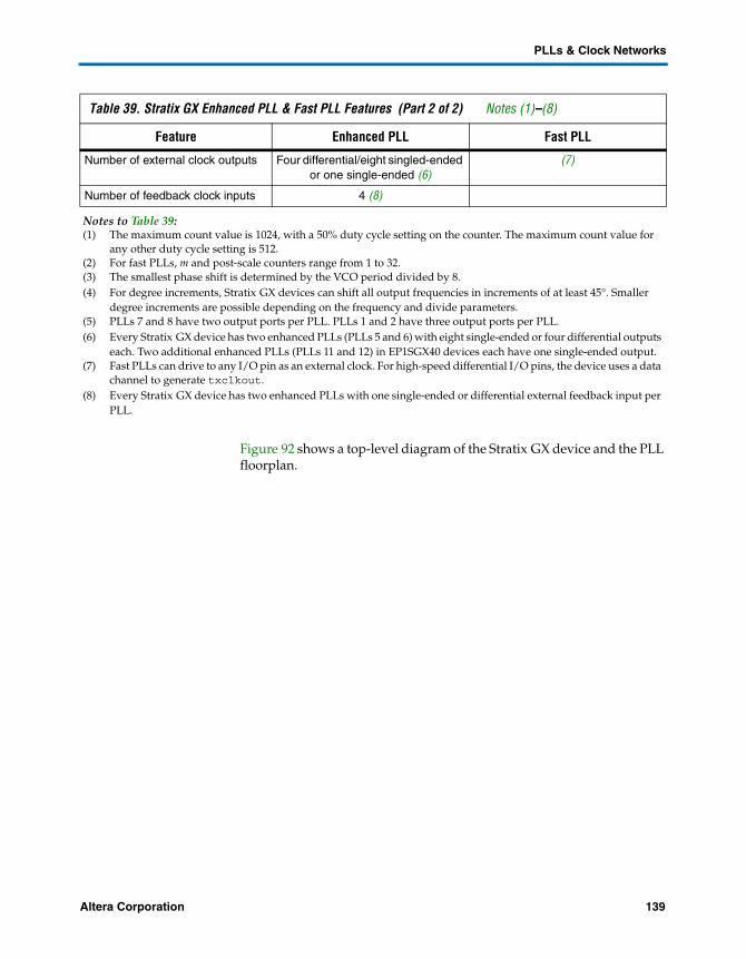
PLLs & Clock Networks
Figure 92 shows a top-level diagram of the Stratix GX device and the PLL floorplan.
Number of external clock outputs Four differential/eight singled-ended or one single-ended (6)
(7)
Number of feedback clock inputs 4 (8)
Notes to Table 39:(1) The maximum count value is 1024, with a 50% duty cycle setting on the counter. The maximum count value for
any other duty cycle setting is 512.(2) For fast PLLs, m and post-scale counters range from 1 to 32.(3) The smallest phase shift is determined by the VCO period divided by 8.(4) For degree increments, Stratix GX devices can shift all output frequencies in increments of at least 45°. Smaller
degree increments are possible depending on the frequency and divide parameters.(5) PLLs 7 and 8 have two output ports per PLL. PLLs 1 and 2 have three output ports per PLL.(6) Every Stratix GX device has two enhanced PLLs (PLLs 5 and 6) with eight single-ended or four differential outputs
each. Two additional enhanced PLLs (PLLs 11 and 12) in EP1SGX40 devices each have one single-ended output.(7) Fast PLLs can drive to any I/O pin as an external clock. For high-speed differential I/O pins, the device uses a data
channel to generate txclkout.(8) Every Stratix GX device has two enhanced PLLs with one single-ended or differential external feedback input per
PLL.
Table 39. Stratix GX Enhanced PLL & Fast PLL Features (Part 2 of 2) Notes (1)–(8)
Feature Enhanced PLL Fast PLL
Altera Corporation 139Preliminary

Stratix GX FPGA Family
Figure 92. PLL Floorplan
Figure 93 shows the global and regional clock connections from the PLL outputs and the CLK pins.
FPLL7CLK
FPLL8CLK
CLK[3..0]
7
1
2
8
115
126
CLK[7..4]
CLK[15..12]
PLLs
High-SpeedTransceivers
inclk1
inclk2
inclk3
inclk4
inclk5
140 Altera CorporationPreliminary
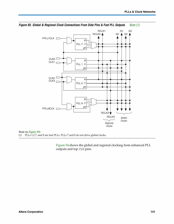
PLLs & Clock Networks
Figure 93. Global & Regional Clock Connections From Side Pins & Fast PLL Outputs Note (1)
Note to Figure 93:(1) PLLs 1,2 7, and 8 are fast PLLs. PLLs 7 and 8 do not drive global clocks.
Figure 94 shows the global and regional clocking from enhanced PLL outputs and top CLK pins.
2
CLK0CLK1
CLK2CLK3
G0
FPLL7CLK
G1G2
G3RCLK0
RCLK1
RCLK2
RCLK3 GlobalClocks
PLL 7
l0
l1
g0
PLL 1
PLL 2
FPLL8CLK
PLL 8
RegionalClocks
l0
l1
g0
l0
l1
g0
l0
l1
g0
Altera Corporation 141Preliminary
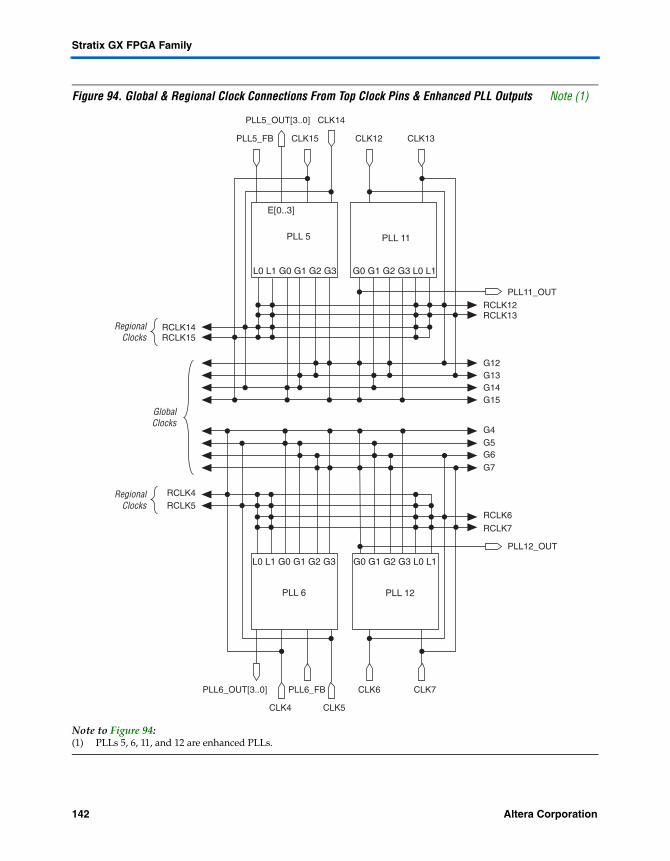
Stratix GX FPGA Family
Figure 94. Global & Regional Clock Connections From Top Clock Pins & Enhanced PLL Outputs Note (1)
Note to Figure 94:(1) PLLs 5, 6, 11, and 12 are enhanced PLLs.
G12G13G14G15
RCLK12RCLK13
RCLK14RCLK15
G7
G6G5G4
RCLK7
RCLK6RCLK5RCLK4
PLL 12
L0 L1 G0 G1 G2 G3
CLK7CLK6
CLK5CLK4
PLL 6
G0 G1 G2 G3 L0 L1
PLL 11
L0 L1 G0 G1 G2 G3
CLK13CLK12
CLK14
CLK15
PLL 5
G0 G1 G2 G3 L0 L1
E[0..3]
PLL12_OUT
PLL6_OUT[3..0]
PLL11_OUT
PLL5_OUT[3..0]
PLL5_FB
PLL6_FB
GlobalClocks
RegionalClocks
RegionalClocks
142 Altera CorporationPreliminary

PLLs & Clock Networks
Enhanced PLLs
Stratix GX devices contain up to four enhanced PLLs with advanced clock management features. Figure 95 shows a diagram of the enhanced PLL.
Figure 95. Stratix GX Enhanced PLL
Notes to Figure 95:(1) External feedback is available in PLLs 5 and 6.(2) This external output is available from the g0 counter for PLLs 11 and 12.(3) These counters and external outputs are available in PLLs 5 and 6.
/n ChargePump VCO /g0
/g1
/g2
/e0
8
4
GlobalClocks
/e1
/e2
I/O Buffers (3)
/e3 ∆t
∆t
∆t
∆t
∆t
∆t
∆t
∆t
Lock Detect to I/O or generalrouting
CLK0
CLK1
FBIN
PFD
/g3
/l1
/l0
From Adjacent PLL
/m
SpreadSpectrum
I/O Buffers (2)(1)
LoopFilter
& Filter
Programmable Time Delay on Each PLL Port
Post-ScaleCounters
ClockSwitch-Over
Circuitry Phase FrequencyDetector
VCO Phase SelectionSelectable at EachPLL Output Port
VCO Phase SelectionAffecting All Outputs
∆t
∆t
∆t
∆t
RegionalClocks
4
Altera Corporation 143Preliminary
Stratix GX FPGA Family
Clock Multiplication & Division
Each Stratix GX device enhanced PLL provides clock synthesis for PLL output ports using m/(n × post-scale counter) scaling factors. The input clock is divided by a pre-scale divider, n, and is then multiplied by the m feedback factor. The control loop drives the VCO to match fIN × (m/n). Each output port has a unique post-scale counter that divides down the high-frequency VCO. For multiple PLL outputs with different frequencies, the VCO is set to the least common multiple of the output frequencies that meets its frequency specifications. Then, the post-scale dividers scale down the output frequency for each output port. For example, if output frequencies required from one PLL are 33 and 66 MHz, set the VCO to 330 MHz (the least common multiple in the VCO’s range). There is one pre-scale divider, n, and one multiply divider, m, per PLL, with a range of 1 to 512 on each. There are two post-scale dividers (l) for regional clock output ports, four counters (g) for global clock output ports, and up to four counters (e) for external clock outputs, all ranging from 1 to 512. The Quartus II software automatically chooses the appropriate scaling factors according to the input frequency, multiplication, and division values entered.
Clock Switchover
To effectively develop high-reliability network systems, clocking schemes must support multiple clocks to provide redundancy. For this reason, Stratix GX device enhanced PLLs support a flexible clock switchover capability. Figure 96 shows a block diagram of the switchover circuit.The switchover circuit is configurable, so designers can define how to implement it. Clock-sense circuitry automatically switches from the primary to secondary clock for PLL reference when the primary clock signal is not present.
144 Altera CorporationPreliminary

PLLs & Clock Networks
Figure 96. Clock Switchover Circuitry
Note to Figure 96:(1) PFD: phase frequency detector.
There are two possible ways to use the clock switchover feature.
Designers can use automatic switchover circuitry for switching between inputs of the same frequency. For example, in applications that require a redundant clock with the same frequency as the primary clock, the switchover state machine generates a signal that controls the multiplexer select input on the bottom of Figure 96. In this case, the secondary clock becomes the reference clock for the PLL.
Designers can use the clkswitch input for user- or system-controlled switch conditions. This is possible for same-frequency switchover or to switch between inputs of different frequencies. For example, if inclk0 is 66 MHz and inclk1 is 100 MHz, designers must control the switchover because the automatic clock-sense circuitry cannot monitor primary and secondary clock frequencies with a frequency difference of more than ±20%. This feature is useful
n Counter
CLKLOSS
CLK0
CLK1
CLK1_BAD
CLK0_BAD
CLKSWITCH
PFD
FBCLK
ClockSense
SMCLKSW
Enhanced PLL
Active Clock
Switch-OverState Machine
∆t
MUXOUT
Altera Corporation 145Preliminary

Stratix GX FPGA Family
when clock sources can originate from multiple cards on the backplane, requiring a system-controlled switchover between frequencies of operation. Designers can use clkswitch together with the lock signal to trigger the switch from a clock that is running but becomes unstable and cannot be locked onto.
During switchover, the PLL VCO continues to run and will either slow down or speed up, generating frequency drift on the PLL outputs. The clock switchover transitions without any glitches. After the switch, there is a finite resynchronization period to lock onto new clock as the VCO ramps up. The exact amount of time it takes for the PLL to relock relates to the PLL configuration and may be adjusted by using the programmable bandwidth feature of the PLL. The preliminary specification for the maximum time to relock is 100 µs.
f For more information on clock switchover, see AN313: Implementing Clock Switchover in Stratix & Stratix GX Devices.
PLL Reconfiguration
The PLL reconfiguration feature enables system logic to change Stratix GX device enhanced PLL counters and delay elements without reloading a Programmer Object File (.pof). This provides considerable flexibility for frequency synthesis, allowing real-time PLL frequency and output clock delay variation. The designer can sweep the PLL output frequencies and clock delay in prototype environments. The PLL reconfiguration feature can also dynamically or intelligently control system clock speeds or tCO delays in end systems.
Clock delay elements at each PLL output port implement variable delay. Figure 97 shows a diagram of the overall dynamic PLL control feature for the counters and the clock delay elements. The configuration time is less than 20 µs for the enhanced PLL using a input shift clock rate of 25 MHz. The charge pump, loop filter components, and phase shifting using VCO phase taps cannot be dynamically adjusted.
146 Altera CorporationPreliminary
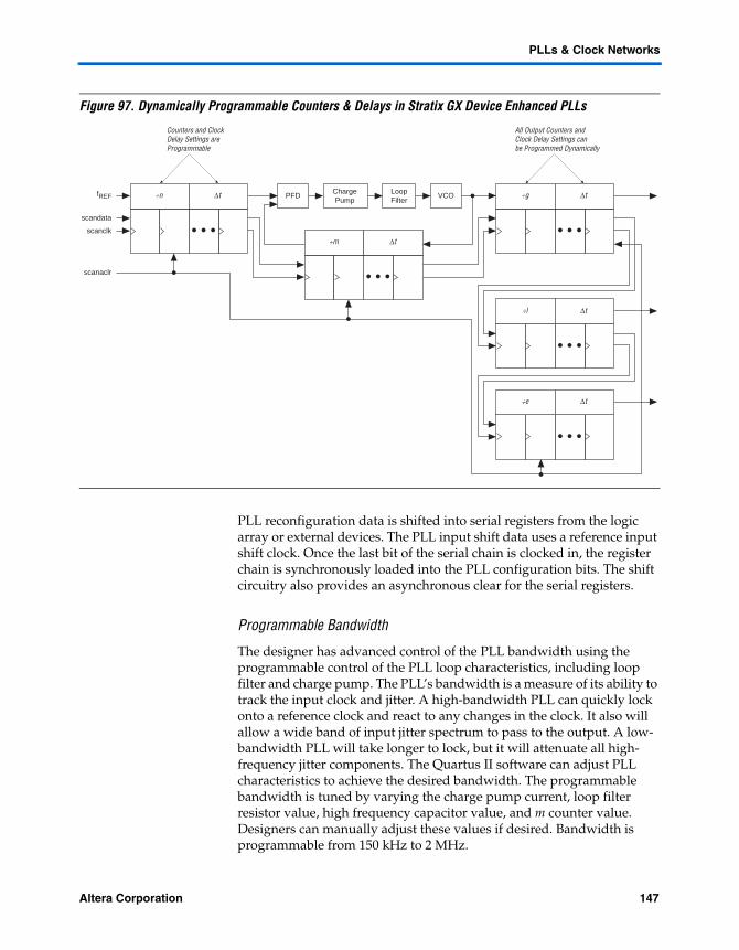
PLLs & Clock Networks
Figure 97. Dynamically Programmable Counters & Delays in Stratix GX Device Enhanced PLLs
PLL reconfiguration data is shifted into serial registers from the logic array or external devices. The PLL input shift data uses a reference input shift clock. Once the last bit of the serial chain is clocked in, the register chain is synchronously loaded into the PLL configuration bits. The shift circuitry also provides an asynchronous clear for the serial registers.
Programmable Bandwidth
The designer has advanced control of the PLL bandwidth using the programmable control of the PLL loop characteristics, including loop filter and charge pump. The PLL’s bandwidth is a measure of its ability to track the input clock and jitter. A high-bandwidth PLL can quickly lock onto a reference clock and react to any changes in the clock. It also will allow a wide band of input jitter spectrum to pass to the output. A low-bandwidth PLL will take longer to lock, but it will attenuate all high-frequency jitter components. The Quartus II software can adjust PLL characteristics to achieve the desired bandwidth. The programmable bandwidth is tuned by varying the charge pump current, loop filter resistor value, high frequency capacitor value, and m counter value. Designers can manually adjust these values if desired. Bandwidth is programmable from 150 kHz to 2 MHz.
÷n ∆t
∆t÷m
÷g ∆t
÷l ∆t
÷e ∆t
PFD VCOChargePump
LoopFilter
fREF
scandata
scanclk
scanaclr
Counters and ClockDelay Settings areProgrammable
All Output Counters andClock Delay Settings canbe Programmed Dynamically
Altera Corporation 147Preliminary
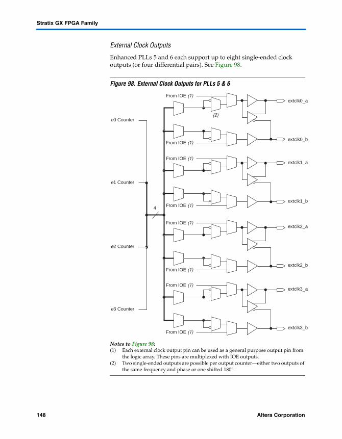
Stratix GX FPGA Family
External Clock Outputs
Enhanced PLLs 5 and 6 each support up to eight single-ended clock outputs (or four differential pairs). See Figure 98.
Figure 98. External Clock Outputs for PLLs 5 & 6
Notes to Figure 98:(1) Each external clock output pin can be used as a general purpose output pin from
the logic array. These pins are multiplexed with IOE outputs.(2) Two single-ended outputs are possible per output counter—either two outputs of
the same frequency and phase or one shifted 180°.
e0 Counter
extclk0_a
extclk0_b
extclk1_a
extclk1_b
extclk2_a
extclk2_b
extclk3_a
extclk3_b
e1 Counter
e2 Counter
e3 Counter
From IOE (1)
From IOE (1)
From IOE (1)
From IOE (1)
From IOE (1)
From IOE (1)
From IOE (1)
From IOE (1)4
(2)
148 Altera CorporationPreliminary

PLLs & Clock Networks
Any of the four external output counters can drive the single-ended or differential clock outputs for PLLs 5 and 6. This means one counter or frequency can drive all output pins available from PLL 5 or PLL 6. Each pair of output pins (four pins total) has dedicated VCC and GND pins to reduce the output clock’s overall jitter by providing improved isolation from switching I/O pins.
For PLLs 5 and 6, each pin of a single-ended output pair can either be in phase or 180° out of phase. The clock output pin pairs support the same I/O standards as standard output pins (in the top and bottom banks) as well as LVDS, LVPECL, 3.3-V PCML, HyperTransport technology, differential HSTL, and differential SSTL. Table 40 shows which I/O standards the enhanced PLL clock pins support. When in single-ended or differential mode, the two outputs operate off the same power supply. Both outputs use the same standards in single-ended mode to maintain performance. Designers can also use the external clock output pins as user output pins if external enhanced PLL clocking is not needed.
Table 40. I/O Standards Supported for Enhanced PLL Pins (Part 1 of 2)
I/O StandardInput Output
INCLK FBIN PLLENABLE EXTCLK
LVTTL v v v v
LVCMOS v v v v
2.5 V v v v
1.8 V v v v
1.5 V v v v
3.3-V PCI v v v
3.3-V PCI-X v v v
LVPECL v v v
3.3-V PCML v v v
LVDS v v v
HyperTransport technology v v v
Differential HSTL v v
Differential SSTL v
3.3-V GTL v v v
3.3-V GTL+ v v v
1.5-V HSTL class I v v v
1.5-V HSTL class II v v v
SSTL-18 class I v v v
SSTL-18 class II v v v
Altera Corporation 149Preliminary

Stratix GX FPGA Family
Enhanced PLLs 11 and 12 support one single-ended output each (see Figure 99). These outputs do not have their own VCC and GND signals. Therefore, to minimize jitter, do not place switching I/O pins next to this output pin.
Figure 99. External Clock Outputs for Enhanced PLLs 11 & 12
Note to Figure 99:(1) For PLL 11, this pin is CLK13n; for PLL 12 this pin is CLK7n.
Stratix GX devices can drive any enhanced PLL driven through the global clock or regional clock network to any general I/O pin as an external output clock. The jitter on the output clock is not guaranteed for these cases.
SSTL-2 class I v v v
SSTL-2 class II v v v
SSTL-3 class I v v v
SSTL-3 class II v v v
AGP (1× and 2×) v v v
CTT v v v
Table 40. I/O Standards Supported for Enhanced PLL Pins (Part 2 of 2)
I/O StandardInput Output
INCLK FBIN PLLENABLE EXTCLK
CLK13n, I/O, PLL11_OUTor CLK6n, I/O, PLL12_OUT (1)
From InternalLogic or IOE
g0Counter
150 Altera CorporationPreliminary
PLLs & Clock Networks
Clock Feedback
The following four feedback modes in Stratix GX device enhanced PLLs allow multiplication and/or phase and delay shifting:
Zero delay buffer: The external clock output pin is phase-aligned with the clock input pin for zero delay.
External feedback: The external feedback input pin, FBIN, is phase-aligned with the clock input, CLK, pin. Aligning these clocks allows the designer to remove clock delay and skew between devices. This mode is only possible for PLLs 5 and 6. PLLs 5 and 6 each support feedback for one of the dedicated external outputs, either one single-ended or one differential pair. In this mode, one e counter feeds back to the PLL FBIN input, becoming part of the feedback loop.
Normal mode: If an internal clock is used in this mode, it is phase-aligned to the input clock pin. The external clock output pin will have a phase delay relative to the clock input pin if connected in this mode. The designer defines which internal clock output from the PLL should be phase-aligned to the internal clock pin.
No compensation: In this mode, the PLL will not compensate for any clock networks or external clock outputs.
Phase & Delay Shifting
Stratix GX device enhanced PLLs provide advanced programmable phase and clock delay shifting. For phase shifting, designers can specify a phase shift (in degrees or time units) for each PLL clock output port or for all outputs together in one shift. Phase-shifting values in time units are allowed with a resolution range of 160 to 420 ps. This resolution is a function of frequency input and the multiplication and division factors. In other words, it is a function of the VCO period equal to one-eighth of the VCO period. Each clock output counter can choose a different phase of the VCO period from up to eight taps. Designers can use this clock output counter along with an initial setting on the post-scale counter to achieve a phase-shift range for the entire period of the output clock. The phase tap feedback to the m counter can shift all outputs to a single phase or delay. The Quartus II software automatically sets the phase taps and counter settings according to the phase shift entered.
Altera Corporation 151Preliminary
Stratix GX FPGA Family
In addition to the phase-shift feature, the fine tune clock delay shift feature provides advanced time delay shift control on each of the four PLL outputs. Each PLL output shifts in 250-ps increments for a range of–3.0 ns to +3.0 ns between any two outputs using discrete delay elements. Total delay shift between any two PLL outputs must be less than 3 ns. For example, shifts on outputs of –1 and +2 ns is allowed, but not –1 and +2.5 ns. There is some delay variation due to process, voltage, and temperature. Only the clock delay shift blocks can be controlled during system operation for dynamic clock delay control.
Spread-Spectrum Clocking
The Stratix GX device’s enhanced PLLs use spread-spectrum technology to reduce electromagnetic interference generation from a system by distributing the energy over a broader frequency range. The enhanced PLL typically provides 0.5% down spread modulation using a triangular profile. The modulation frequency is programmable. Enabling spread spectrum for a PLL affects all of its outputs.
Lock Detect
The lock output indicates that there is a stable clock output signal in phase with the reference clock. Without any additional circuitry, the lock signal may toggle as the PLL begins tracking the reference clock. Designers may need to gate the lock signal for use as a system control. The lock signal from the locked port can drive the logic array or an output pin.
Whenever the PLL loses lock for any reason (be it excessive inclk jitter, clock switchover, PLL reconfiguration, power supply noise etc.), the PLL must be reset with the areset signal for correct phase shift operation. If the phase relationship between the input clock versus output clock, and between different output clocks from the PLL is not important in the design, then the PLL need not be reset.
f See the Stratix GX FPGA Errata Sheet for more information on implementing the gated lock signal in the design.
Programmable Duty Cycle
The programmable duty cycle allows enhanced PLLs to generate clock outputs with a variable duty cycle. This feature is supported on each enhanced PLL post-scale counter (g0..g3, l0..l3, e0..e3). The duty cycle setting is achieved by a low and high time count setting for the post-scale dividers. The Quartus II software uses the frequency input and the required multiply or divide rate to determine the duty cycle choices.
152 Altera CorporationPreliminary

PLLs & Clock Networks
Advanced Clear & Enable Control
There are several control signals for clearing and enabling PLLs and their outputs. Designers can use these signals to control PLL resynchronization and gate PLL output clocks for low-power applications.
The pllenable pin is a dedicated pin that enables/disables PLLs. When the pllenable pin is low, the clock output ports are driven by GND and all the PLLs go out of lock. When the pllenable pin goes high again, the PLLs relock and resynchronize to the input clocks. Designers can choose which PLLs are controlled by the pllenable signal by connecting the pllenable input port of the altpll megafunction to the common pllenable input pin.
The areset signals are reset/resynchronization inputs for each PLL. The areset signal should be asserted every time the PLL loses lock to guarantee correct phase relationship between the PLL output clocks. Users should include the areset signal in designs if any of the following conditions are true:
PLL Reconfiguration or Clock switchover enables in the design. Phase relationships between output clocks need to be maintained
after a loss of lock condition
The device input pins or logic elements (LEs) can drive these input signals. When driven high, the PLL counters resets, clearing the PLL output and placing the PLL out of lock. The VCO sets back to its nominal setting (~700 MHz). When driven low again, the PLL resynchronizes to its input as it relocks. If the target VCO frequency is below this nominal frequency, then the output frequency starts at a higher value than desired as the PLL locks. If the system cannot tolerate this, the clkena signal can disable the output clocks until the PLL locks.
The pfdena signals control the phase frequency detector (PFD) output with a programmable gate. If designers disable the PFD, the VCO will operate at its last set value of control voltage and frequency with some long-term drift to a lower frequency. The system will continue running when the PLL goes out of lock or the input clock is disabled. By maintaining the last locked frequency, the system has time to store its current settings before shutting down. Designers can either use their own control signal or a clkloss status signal to trigger pfdena.
Altera Corporation 153Preliminary
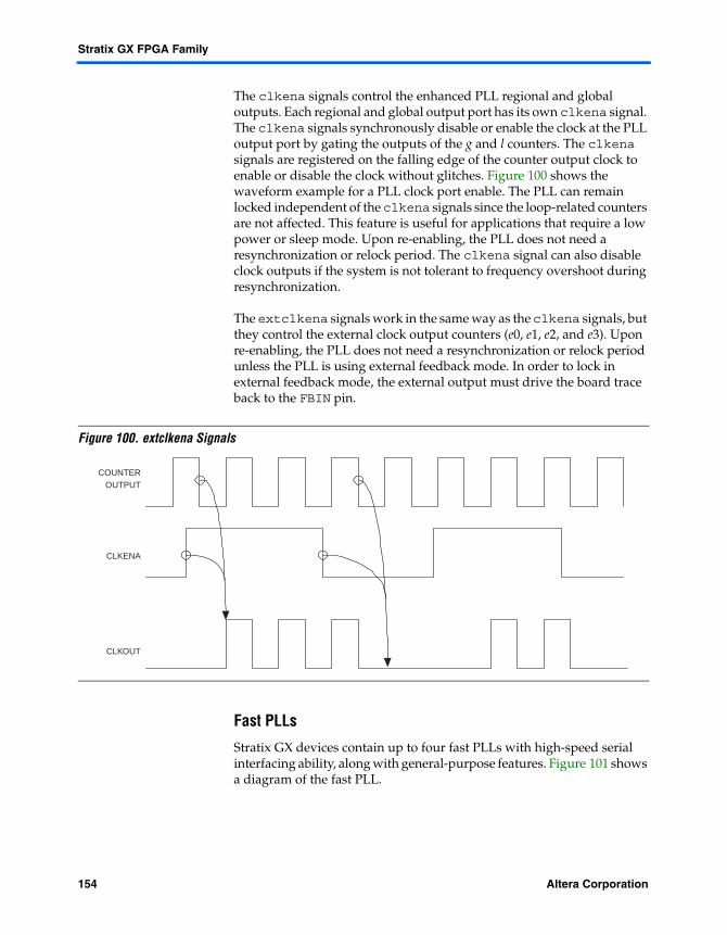
Stratix GX FPGA Family
The clkena signals control the enhanced PLL regional and global outputs. Each regional and global output port has its own clkena signal. The clkena signals synchronously disable or enable the clock at the PLL output port by gating the outputs of the g and l counters. The clkena signals are registered on the falling edge of the counter output clock to enable or disable the clock without glitches. Figure 100 shows the waveform example for a PLL clock port enable. The PLL can remain locked independent of the clkena signals since the loop-related counters are not affected. This feature is useful for applications that require a low power or sleep mode. Upon re-enabling, the PLL does not need a resynchronization or relock period. The clkena signal can also disable clock outputs if the system is not tolerant to frequency overshoot during resynchronization.
The extclkena signals work in the same way as the clkena signals, but they control the external clock output counters (e0, e1, e2, and e3). Upon re-enabling, the PLL does not need a resynchronization or relock period unless the PLL is using external feedback mode. In order to lock in external feedback mode, the external output must drive the board trace back to the FBIN pin.
Figure 100. extclkena Signals
Fast PLLs
Stratix GX devices contain up to four fast PLLs with high-speed serial interfacing ability, along with general-purpose features. Figure 101 shows a diagram of the fast PLL.
COUNTEROUTPUT
CLKENA
CLKOUT
154 Altera CorporationPreliminary
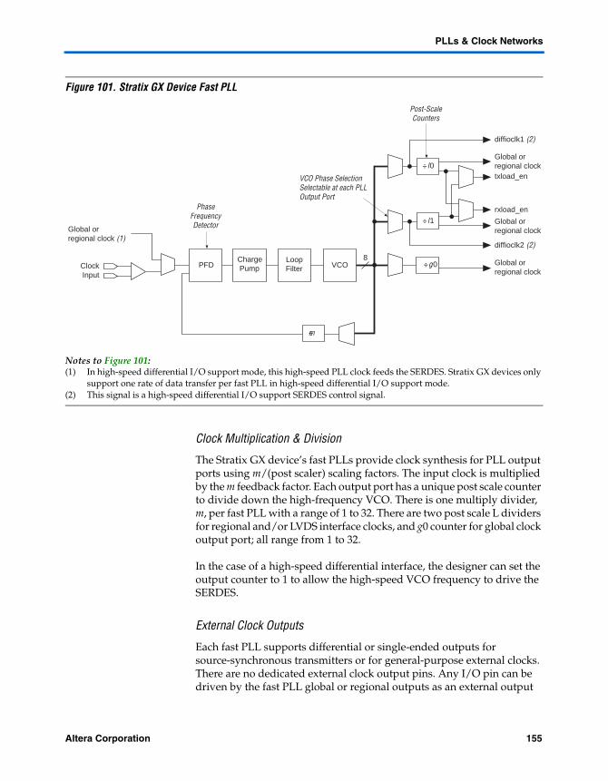
PLLs & Clock Networks
Figure 101. Stratix GX Device Fast PLL
Notes to Figure 101:(1) In high-speed differential I/O support mode, this high-speed PLL clock feeds the SERDES. Stratix GX devices only
support one rate of data transfer per fast PLL in high-speed differential I/O support mode.(2) This signal is a high-speed differential I/O support SERDES control signal.
Clock Multiplication & Division
The Stratix GX device’s fast PLLs provide clock synthesis for PLL output ports using m/(post scaler) scaling factors. The input clock is multiplied by the m feedback factor. Each output port has a unique post scale counter to divide down the high-frequency VCO. There is one multiply divider, m, per fast PLL with a range of 1 to 32. There are two post scale L dividers for regional and/or LVDS interface clocks, and g0 counter for global clock output port; all range from 1 to 32.
In the case of a high-speed differential interface, the designer can set the output counter to 1 to allow the high-speed VCO frequency to drive the SERDES.
External Clock Outputs
Each fast PLL supports differential or single-ended outputs for source-synchronous transmitters or for general-purpose external clocks. There are no dedicated external clock output pins. Any I/O pin can be driven by the fast PLL global or regional outputs as an external output
ChargePump VCO ÷g0
8ClockInput
PFD
÷ l1
÷ l0
÷m
LoopFilter
PhaseFrequencyDetector
VCO Phase SelectionSelectable at each PLLOutput Port
Post-ScaleCounters
Global orregional clock
Global orregional clock
Global orregional clock
diffioclk2 (2)
diffioclk1 (2)
txload_en
rxload_en
Global orregional clock (1)
Altera Corporation 155Preliminary
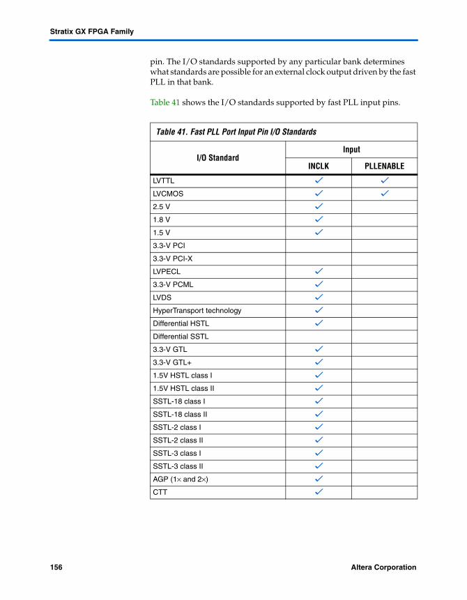
Stratix GX FPGA Family
pin. The I/O standards supported by any particular bank determines what standards are possible for an external clock output driven by the fast PLL in that bank.
Table 41 shows the I/O standards supported by fast PLL input pins.
Table 41. Fast PLL Port Input Pin I/O Standards
I/O StandardInput
INCLK PLLENABLE
LVTTL v v
LVCMOS v v
2.5 V v
1.8 V v
1.5 V v
3.3-V PCI
3.3-V PCI-X
LVPECL v
3.3-V PCML v
LVDS v
HyperTransport technology v
Differential HSTL v
Differential SSTL
3.3-V GTL v
3.3-V GTL+ v
1.5V HSTL class I v
1.5V HSTL class II v
SSTL-18 class I v
SSTL-18 class II v
SSTL-2 class I v
SSTL-2 class II v
SSTL-3 class I v
SSTL-3 class II v
AGP (1× and 2×) v
CTT v
156 Altera CorporationPreliminary
I/O Structure
Phase Shifting
Stratix GX device fast PLLs have advanced clock shift capability that enables programmable phase shifts. Designers can enter a phase shift (in degrees or time units) for each PLL clock output port or for all outputs together in one shift. Designers can perform phase shifting in time units with a resolution range of 150 to 400 ps. This resolution is a function of the VCO period.
Control Signals
The fast PLL has the same lock output, pllenable input, and areset input control signals as the enhanced PLL.
For more information on high-speed differential I/O support, see “Source-Synchronous Signaling with DPA” on page 46.
I/O Structure IOEs provide many features, including:
Dedicated differential and single-ended I/O buffers 3.3-V, 64-bit, 66-MHz PCI compliance 3.3-V, 64-bit, 133-MHz PCI-X 1.0 compliance Joint Test Action Group (JTAG) boundary-scan test (BST) support Differential on-chip termination for LVDS I/O standard Programmable pull-up during configuration Output drive strength control Slew-rate control Tri-state buffers Bus-hold circuitry Programmable pull-up resistors Programmable input and output delays Open-drain outputs DQ and DQS I/O pins Double-data rate (DDR) Registers
The IOE in Stratix GX devices contains a bidirectional I/O buffer, six registers, and a latch for a complete embedded bidirectional single data rate or DDR transfer. Figure 102 shows the Stratix GX IOE structure. The IOE contains two input registers (plus a latch), two output registers, and two output enable registers. The design can use both input registers and the latch to capture DDR input and both output registers to drive DDR outputs. Additionally, the design can use the output enable (OE) register for fast clock-to-output enable timing. The negative edge-clocked OE register is used for DDR SDRAM interfacing. The Quartus II software automatically duplicates a single OE register that controls multiple output or bidirectional pins.
Altera Corporation 157Preliminary

Stratix GX FPGA Family
Figure 102. Stratix GX IOE Structure
The IOEs are located in I/O blocks around the periphery of the Stratix GX device. There are up to four IOEs per row I/O block and six IOEs per column I/O block. The row I/O blocks drive row, column, or direct link interconnects. The column I/O blocks drive column interconnects. Figure 103 shows how a row I/O block connects to the logic array. Figure 104 shows how a column I/O block connects to the logic array.
D Q
Output Register
Output A
D Q
Output Register
Output B
Input A
Input B
D Q
OE Register
OE
D Q
OE Register
D Q
Input Register
D Q
Input Register
D Q
Input Latch
Logic Array
CLK
ENA
158 Altera CorporationPreliminary

I/O Structure
Figure 103. Row I/O Block Connection to the Interconnect
Notes to Figure 103:(1) The 16 control signals are composed of four output enables io_boe[3..0], four clock enables io_bce[3..0],
four clocks io_clk[3..0], and four clear signals io_bclr[3..0].(2) The 28 data and control signals consist of eight data out lines: four lines each for DDR applications
io_dataouta[3..0] and io_dataoutb[3..0], four output enables io_coe[3..0], four input clock enables io_cce_in[3..0], four output clock enables io_cce_out[3..0], four clocks io_cclk[3..0], and four clear signals io_cclr[3..0].
16
28
R4, R8 & R24Interconnects
C4, C8 & C16Interconnects
I/O Block Local Interconnect
16 Control Signalsfrom I/O Interconnect (1)
I/O Interconnect
28 Data & Control Signals from Logic Array (2)
io_dataouta[3..0]io_dataoutb[3..0]
io_clk[7:0]
Horizontal I/OBlock Containsup to Four IOEs
Direct LinkInterconnect
to Adjacent LAB
Direct LinkInterconnect
to Adjacent LAB
LAB LocalInterconnect
LAB HorizontalI/O Block
Altera Corporation 159Preliminary

Stratix GX FPGA Family
Figure 104. Column I/O Block Connection to the Interconnect
Notes to Figure 104:(1) The 16 control signals are composed of four output enables io_boe[3..0], four clock enables io_bce[3..0],
four clocks io_bclk[3..0], and four clear signals io_bclr[3..0].(2) The 42 data and control signals consist of 12 data out lines; six lines each for DDR applications
io_dataouta[5..0] and io_dataoutb[5..0], six output enables io_coe[5..0], six input clock enables io_cce_in[5..0], six output clock enables io_cce_out[5..0], six clocks io_cclk[5..0], and six clear signals io_cclr[5..0].
16 Control Signals from I/O Interconnect (1)
42 Data &Control Signals
from Logic Array (2) Vertical I/O Block Containsup to Six IOEs
I/O BlockLocal Interconnect
I/O Interconnect
IO_datain[3:0]
R4, R8 & R24Interconnects
LAB LocalInterconnect
C4, C8 & C16Interconnects
16 42
LAB LAB LAB
io_clk[7..0]
Vertical I/O Block
160 Altera CorporationPreliminary

I/O Structure
Stratix GX devices have an I/O interconnect similar to the R4 and C4 interconnect to drive high-fanout signals to and from the I/O blocks. There are 16 signals that drive into the I/O blocks composed of four output enables io_boe[3..0], four clock enables io_bce[3..0], four clocks io_bclk[3..0], and four clear signals io_bclr[3..0]. The pin’s datain signals can drive the IO interconnect, which in turn drives the logic array or other I/O blocks. In addition, the control and data signals can be driven from the logic array, providing a slower but more flexible routing resource. The row or column IOE clocks, io_clk[7..0], provide a dedicated routing resource for low-skew, high-speed clocks. I/O clocks are generated from regional, global, or fast regional clocks (see “PLLs & Clock Networks” on page 129). Figure 105 illustrates the signal paths through the I/O block.
Figure 105. Signal Path Through the I/O Block
Each IOE contains its own control signal selection for the following control signals: oe, ce_in, ce_out, aclr/preset, sclr/preset, clk_in, and clk_out. Figure 106 illustrates the control signal selection.
Row or Columnio_clk[7..0]
io_boe[3..0]
io_bce[3..0]
io_bclk[3..0]
io_bclr[3..0]
io_datain0
io_datain1
io_dataout0
io_dataout1
io_coe
oe
ce_in
ce_out
io_cce_inaclr/preset
io_cce_outsclr
io_cclrclk_in
io_cclkclk_out
ControlSignal
Selection
IOE
From I/OInterconnect
To LogicArray
From LogicArray
To OtherIOEs
Altera Corporation 161Preliminary

Stratix GX FPGA Family
Figure 106. Control Signal Selection per IOE
In normal bidirectional operation, the input register can be used for input data requiring fast setup times. The input register can have its own clock input and clock enable separate from the OE and output registers. The output register can be used for data requiring fast clock-to-output performance. The OE register can be used for fast clock-to-output enable timing. The OE and output register share the same clock source and the same clock enable source from local interconnect in the associated LAB, dedicated I/O clocks, and the column and row interconnects. Figure 107 shows the IOE in bidirectional configuration.
clk_out
ce_inclk_in
ce_out
aclr/preset
sclr/preset
I/O Interconnect[15..0]
Dedicated I/OClock [7..0]
LocalInterconnect
LocalInterconnect
LocalInterconnect
LocalInterconnect
LocalInterconnect
oe
io_coe
io_cclr
io_cce_out
io_cce_in
io_cclk
io_bclk[3..0] io_bce[3..0] io_bclr[3..0] io_boe[3..0]
162 Altera CorporationPreliminary
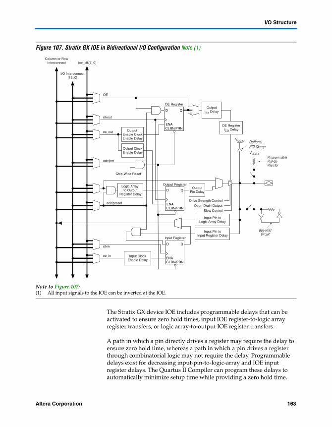
I/O Structure
Figure 107. Stratix GX IOE in Bidirectional I/O Configuration Note (1)
Note to Figure 107:(1) All input signals to the IOE can be inverted at the IOE.
The Stratix GX device IOE includes programmable delays that can be activated to ensure zero hold times, input IOE register-to-logic array register transfers, or logic array-to-output IOE register transfers.
A path in which a pin directly drives a register may require the delay to ensure zero hold time, whereas a path in which a pin drives a register through combinatorial logic may not require the delay. Programmable delays exist for decreasing input-pin-to-logic-array and IOE input register delays. The Quartus II Compiler can program these delays to automatically minimize setup time while providing a zero hold time.
CLRN/PRN
D Q
ENA
Chip-Wide Reset
OE Register
CLRN/PRN
D Q
ENA
Output Register
VCCIO
VCCIO OptionalPCI Clamp
ProgrammablePull-UpResistor
Column or RowInterconnect
I/O Interconnect[15..0]
ioe_clk[7..0]
Bus-HoldCircuit
Output Enable ClockEnable Delay
Output ClockEnable Delay
Logic Array to Output
Register Delay
OutputtZX Delay
OE RegistertCO Delay
CLRN/PRN
D Q
ENA
Input Register
Input ClockEnable Delay
Input Pin toInput Register Delay
Input Pin toLogic Array Delay
Drive Strength Control
Open-Drain Output
Slew Control
sclr/preset
OE
clkout
ce_out
aclr/prn
clkin
ce_in
OutputPin Delay
Altera Corporation 163Preliminary

Stratix GX FPGA Family
Programmable delays can increase the register-to-pin delays for output and/or output enable registers. A programmable delay exists to increase the tZX delay to the output pin, which is required for ZBT interfaces. Table 42 shows the programmable delays for Stratix GX devices.
The IOE registers in Stratix GX devices share the same source for clear or preset. The designer can program preset or clear for each individual IOE. The designer can also program the registers to power up high or low after configuration is complete. If programmed to power up low, an asynchronous clear can control the registers. If programmed to power up high, an asynchronous preset can control the registers. This feature prevents the inadvertent activation of another device’s active-low input upon power-up. If one register in an IOE uses a preset or clear signal then all registers in the IOE must use that same signal if they require preset or clear. Additionally a synchronous reset signal is available to the designer for the IOE registers.
Double-Data Rate I/O Pins
Stratix GX devices have six registers in the IOE, which support DDR interfacing by clocking data on both positive and negative clock edges. The IOEs in Stratix GX devices support DDR inputs, DDR outputs, and bidirectional DDR modes.
Table 42. Stratix GX Programmable Delay Chain
Programmable Delays Quartus II Logic Option
Input pin to logic array delay Decrease input delay to internal cells
Input pin to input register delay Decrease input delay to input register
Output pin delay Increase delay to output pin
Output enable register tCO delay Increase delay to output enable pin
Output tZX delay Increase tZX delay to output pin
Output clock enable delay Increase output clock enable delay
Input clock enable delay Increase input clock enable delay
Logic array to output register delay Decrease input delay to output register
Output enable clock enable delay Increase output enable clock enable delay
164 Altera CorporationPreliminary

I/O Structure
When using the IOE for DDR inputs, the two input registers clock double rate input data on alternating edges. An input latch is also used within the IOE for DDR input acquisition. The latch holds the data that is present during the clock high times. This allows both bits of data to be synchronous with the same clock edge (either rising or falling). Figure 108 shows an IOE configured for DDR input. Figure 109 shows the DDR input timing diagram.
Figure 108. Stratix GX IOE in DDR Input I/O Configuration Note (1)
Notes to Figure 108:(1) All input signals to the IOE can be inverted at the IOE.(2) This signal connection is only allowed on dedicated DQ function pins.(3) This signal is for dedicated DQS function pins only.
CLRN/PRN
D Q
ENA
Chip-Wide Reset
Input Register
CLRN/PRN
D Q
ENA
Input Register
VCCIO
VCCIO
OptionalPCI Clamp
ProgrammablePull-UpResistor
Column or RowInterconnect
I/O Interconnect[15..0]
DQS LocalBus (1), (2)
To DQS LocalBus (3)
ioe_clk[7..0]
Bus-HoldCircuit
Output ClockEnable Delay
CLRN/PRN
D Q
ENA
Latch
Input Pin toInput Register Delay
sclr
clkin
aclr/prn
(1)
(1)
Altera Corporation 165Preliminary
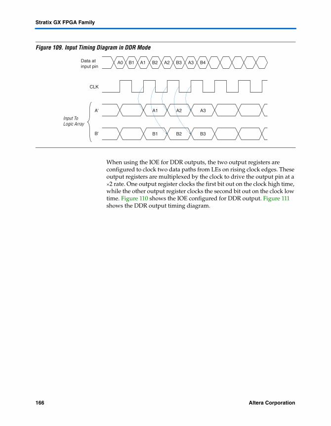
Stratix GX FPGA Family
Figure 109. Input Timing Diagram in DDR Mode
When using the IOE for DDR outputs, the two output registers are configured to clock two data paths from LEs on rising clock edges. These output registers are multiplexed by the clock to drive the output pin at a ×2 rate. One output register clocks the first bit out on the clock high time, while the other output register clocks the second bit out on the clock low time. Figure 110 shows the IOE configured for DDR output. Figure 111 shows the DDR output timing diagram.
Data atinput pin
A'
B'
CLK
A0 B1 A1
A1
B2 A2 A3
A2 A3
B1 B2 B3
B3 B4
Input ToLogic Array
166 Altera CorporationPreliminary
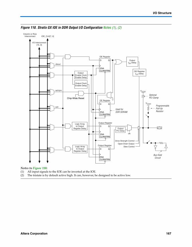
I/O Structure
Figure 110. Stratix GX IOE in DDR Output I/O Configuration Notes (1), (2)
Notes to Figure 110:(1) All input signals to the IOE can be inverted at the IOE.(2) The tristate is by default active high. It can, however, be designed to be active low.
CLRN/PRN
D Q
ENA
Chip-Wide Reset
OE Register
CLRN/PRN
D Q
ENA
OE Register
CLRN/PRN
D Q
ENA
Output Register
VCCIO
VCCIO
OptionalPCI Clamp
ProgrammablePull-UpResistor
Column or RowInterconnect
I/O Interconnect[15..0]
IOE_CLK[7..0]
Bus-HoldCircuit
Logic Arrayto Output
Register Delay
OutputtZX Delay
OE RegistertCO Delay
CLRN/PRN
D Q
ENA
Output RegisterLogic Arrayto Output
Register Delay
Drive Strength Control
Open-Drain Output
Slew Control
Used forDDR SDRAM
clk
sclr
aclr/prn
clkout
OutputPin Delay
Output Enable ClockEnable Delay
Output ClockEnable Delay
Altera Corporation 167Preliminary
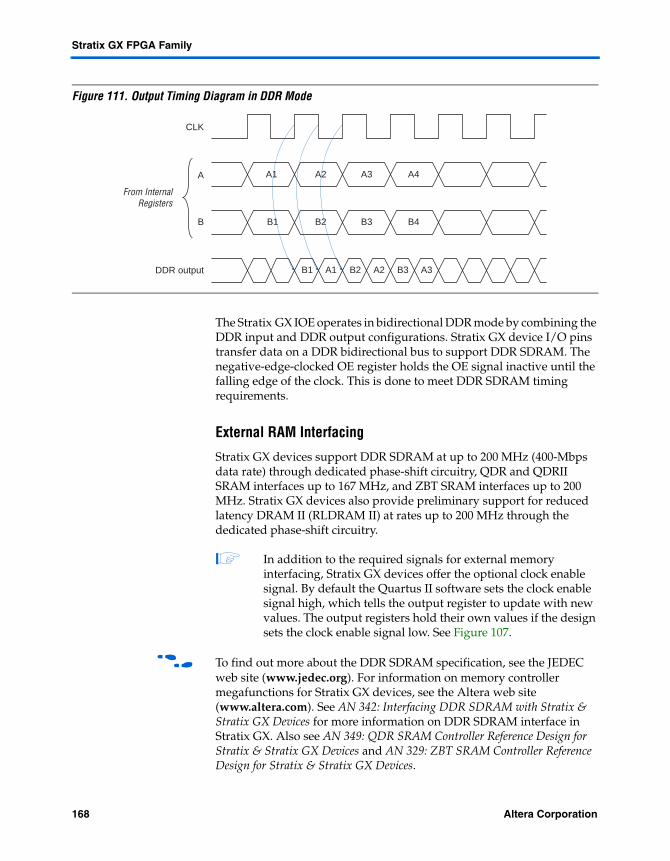
Stratix GX FPGA Family
Figure 111. Output Timing Diagram in DDR Mode
The Stratix GX IOE operates in bidirectional DDR mode by combining the DDR input and DDR output configurations. Stratix GX device I/O pins transfer data on a DDR bidirectional bus to support DDR SDRAM. The negative-edge-clocked OE register holds the OE signal inactive until the falling edge of the clock. This is done to meet DDR SDRAM timing requirements.
External RAM Interfacing
Stratix GX devices support DDR SDRAM at up to 200 MHz (400-Mbps data rate) through dedicated phase-shift circuitry, QDR and QDRII SRAM interfaces up to 167 MHz, and ZBT SRAM interfaces up to 200 MHz. Stratix GX devices also provide preliminary support for reduced latency DRAM II (RLDRAM II) at rates up to 200 MHz through the dedicated phase-shift circuitry.
1 In addition to the required signals for external memory interfacing, Stratix GX devices offer the optional clock enable signal. By default the Quartus II software sets the clock enable signal high, which tells the output register to update with new values. The output registers hold their own values if the design sets the clock enable signal low. See Figure 107.
f To find out more about the DDR SDRAM specification, see the JEDEC web site (www.jedec.org). For information on memory controller megafunctions for Stratix GX devices, see the Altera web site (www.altera.com). See AN 342: Interfacing DDR SDRAM with Stratix & Stratix GX Devices for more information on DDR SDRAM interface in Stratix GX. Also see AN 349: QDR SRAM Controller Reference Design for Stratix & Stratix GX Devices and AN 329: ZBT SRAM Controller Reference Design for Stratix & Stratix GX Devices.
From InternalRegisters
DDR output
CLK
A
B
B1 A1 B2 A2 B3 A3
A2A1 A3 A4
B1 B2 B3 B4
168 Altera CorporationPreliminary

I/O Structure
Table 43 shows the performance specification for DDR SDRAM, RLDRAM II, QDR SRAM, QDRII SRAM, and ZBT SRAM interfaces in EP1SGX10 through EP1SGX40 devices. The DDR SDRAM and QDR SRAM numbers in Table 43 have been verified with hardware characterization with third-party DDR SDRAM and QDR SRAM devices over temperature and voltage extremes.
In addition to six I/O registers and one input latch in the IOE for interfacing to these high-speed memory interfaces, Stratix GX devices also have dedicated circuitry for interfacing with DDR SDRAM. In every Stratix GX device, the I/O banks at the top (I/O banks 3 and 4) and bottom (I/O banks 7 and 8) of the device support DDR SDRAM up to 200 MHz. These pins support DQS signals with DQ bus modes of ×8, ×16, or ×32.
Table 43. External RAM Support in EP1SGX10 through EP1SGX40 Devices
DDR Memory Type I/O Standard
Maximum Clock Rate (MHz)
-5 Speed Grade -6 Speed Grade -7 Speed Grade
DDR SDRAM (1), (2) SSTL-2 200 167 133
DDR SDRAM - side banks (2), (3), (4)
SSTL-2 150 133 133
RLDRAM II (4) 1.8-V HSTL 200 (5) (5)
QDR SRAM (6) 1.5-V HSTL 167 167 133
QDRII SRAM (6) 1.5-V HSTL 200 167 133
ZBT SRAM (7) LVTTL 200 200 167
Notes to Table 43:(1) These maximum clock rates apply if the Stratix GX device uses DQS phase-shift circuitry to interface with DDR
SDRAM. DQS phase-shift circuitry is only available in the top and bottom I/O banks (I/O banks 3, 4, 7, and 8). (2) For more information on DDR SDRAM, see AN 342: Interfacing DDR SDRAM with Stratix & Stratix GX Devices.(3) DDR SDRAM is supported on the Stratix GX device side I/O banks (I/O banks 1, 2, 5, and 6) without dedicated
DQS phase-shift circuitry. The read DQS signal is ignored in this mode.(4) These performance specifications are preliminary.(5) This device does not support RLDRAM II.(6) For more information on QDR or QDRII SRAM, see AN 349: QDR SRAM Controller Reference Design for Stratix &
Stratix GX Devices.(7) For more information on ZBT SRAM, see AN 329: ZBT SRAM Controller Reference Design for Stratix & Stratix GX
Devices.
Altera Corporation 169Preliminary

Stratix GX FPGA Family
Table 44 shows the number of DQ and DQS buses that are supported per device.
A compensated delay element on each DQS pin automatically aligns input DQS synchronization signals with the data window of their corresponding DQ data signals. The DQS signals drive a local DQS bus in the top and bottom I/O banks. This DQS bus is an additional resource to the I/O clocks and is used to clock DQ input registers with the DQS signal.
Two separate single phase-shifting reference circuits are located on the top and bottom of the Stratix GX device. Each circuit is driven by a system reference clock through the CLK pins that is the same frequency as the DQS signal. Clock pins CLK[15..12]p feed the phase-shift circuitry on the top of the device and clock pins CLK[7..4]p feed the phase-shift circuitry on the bottom of the device. The phase-shifting reference circuit on the top of the device controls the compensated delay elements for all 10 DQS pins located at the top of the device. The phase-shifting reference circuit on the bottom of the device controls the compensated delay elements for all 10 DQS pins located on the bottom of the device. All 10 delay elements (DQS signals) on either the top or bottom of the device shift by the same degree amount. For example, all 10 DQS pins on the top of the device can be shifted by 90° and all 10 DQS pins on the bottom of the device can be shifted by 72°. The reference circuits require a maximum of 256 system reference clock cycles to set the correct phase on the DQS delay elements. Figure 112 illustrates the phase-shift reference circuit control of each DQS delay shift on the top of the device. This same circuit is duplicated on the bottom of the device.
Table 44. DQS & DQ Bus Mode Support Note (1)
Device Package Number of ×8 Groups
Number of ×16 Groups
Number of ×32 Groups
EP1SGX10 672-pin FineLine BGA 12 (2) 0 0
EP1SGX25 672-pin FineLine BGA 16 (3) 8 4
1,020-pin FineLine BGA 20 8 4
EP1SGX40 1,020-pin FineLine BGA 20 8 4
Notes to Table 44:(1) See the Selectable I/O Standards in Stratix & Stratix GX Devices chapter in the Stratix Device Handbook, Volume 2
for VREF guidelines.(2) These packages have six groups in I/O banks 3 and 4 and six groups in I/O banks 7 and 8.(3) These packages have eight groups in I/O banks 3 and 4 and eight groups in I/O banks 7 and 8.
170 Altera CorporationPreliminary

I/O Structure
Figure 112. Simplified Diagram of the DQS Phase-Shift Circuitry
See the External Memory Interfaces chapter in the Stratix Device Handbook, Volume 2 for more information on external memory interfaces.
Programmable Drive Strength
The output buffer for each Stratix GX device I/O pin has a programmable drive strength control for certain I/O standards. The LVTTL and LVCMOS standard has several levels of drive strength that the user can control. SSTL-3 class I and II, SSTL-2 class I and II, HSTL class I and II, and 3.3-V GTL+ support a minimum setting, the lowest drive strength that guarantees the IOH/IOL of the standard. Using minimum settings provides signal slew rate control to reduce system noise and signal overshoot.
PhaseComparator
Up/DownCounter
Delay Chains
InputReference
Clock
Control Signalsto DQS Pins
6
Altera Corporation 171Preliminary
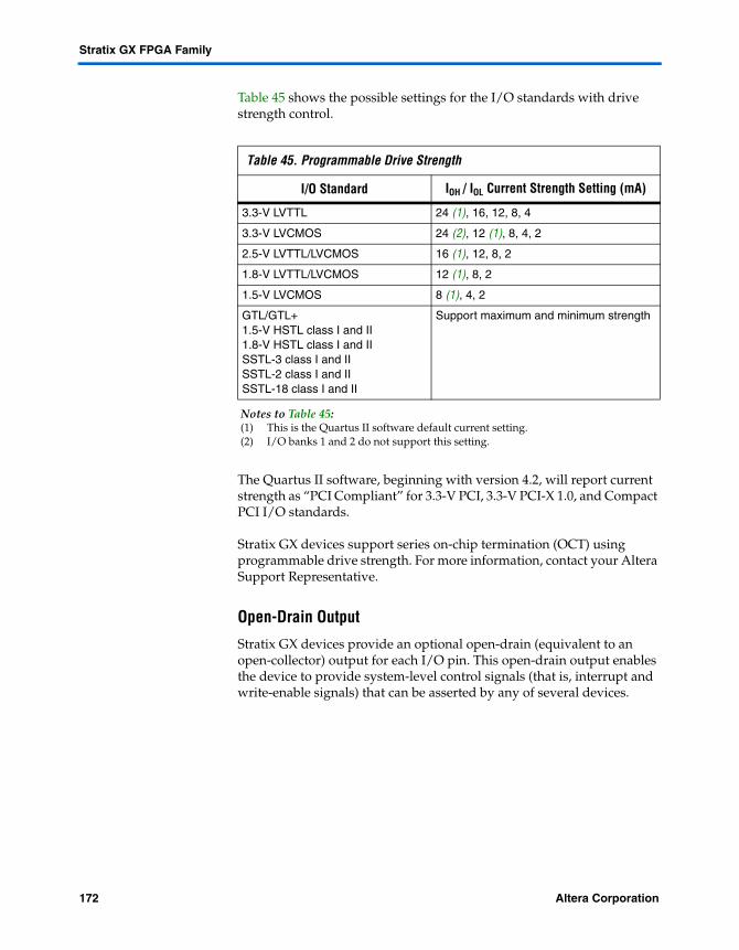
Stratix GX FPGA Family
Table 45 shows the possible settings for the I/O standards with drive strength control.
The Quartus II software, beginning with version 4.2, will report current strength as “PCI Compliant” for 3.3-V PCI, 3.3-V PCI-X 1.0, and Compact PCI I/O standards.
Stratix GX devices support series on-chip termination (OCT) using programmable drive strength. For more information, contact your Altera Support Representative.
Open-Drain Output
Stratix GX devices provide an optional open-drain (equivalent to an open-collector) output for each I/O pin. This open-drain output enables the device to provide system-level control signals (that is, interrupt and write-enable signals) that can be asserted by any of several devices.
Table 45. Programmable Drive Strength
I/O Standard IOH / IOL Current Strength Setting (mA)
3.3-V LVTTL 24 (1), 16, 12, 8, 4
3.3-V LVCMOS 24 (2), 12 (1), 8, 4, 2
2.5-V LVTTL/LVCMOS 16 (1), 12, 8, 2
1.8-V LVTTL/LVCMOS 12 (1), 8, 2
1.5-V LVCMOS 8 (1), 4, 2
GTL/GTL+1.5-V HSTL class I and II1.8-V HSTL class I and IISSTL-3 class I and IISSTL-2 class I and IISSTL-18 class I and II
Support maximum and minimum strength
Notes to Table 45:(1) This is the Quartus II software default current setting.(2) I/O banks 1 and 2 do not support this setting.
172 Altera CorporationPreliminary

I/O Structure
Slew-Rate Control
The output buffer for each Stratix GX device I/O pin has a programmable output slew-rate control that can be configured for low-noise or high-speed performance. A faster slew rate provides high-speed transitions for high-performance systems. However, these fast transitions may introduce noise transients into the system. A slow slew rate reduces system noise, but adds a nominal delay to rising and falling edges. Each I/O pin has an individual slew-rate control, allowing the designer to specify the slew rate on a pin-by-pin basis. The slew-rate control affects both the rising and falling edges.
Bus Hold
Each Stratix GX device I/O pin provides an optional bus-hold feature. The bus-hold circuitry can weakly hold the signal on an I/O pin at its last-driven state. Since the bus-hold feature holds the last-driven state of the pin until the next input signal is present, an external pull-up or pull-down resistor is not needed to hold a signal level when the bus is tri-stated.
Table 46 shows bus hold support for different pin types.
The bus-hold circuitry also pulls undriven pins away from the input threshold voltage where noise can cause unintended high-frequency switching. The designer can select this feature individually for each I/O pin. The bus-hold output will drive no higher than VCCIO to prevent overdriving signals. If the bus-hold feature is enabled, the programmable pull-up option cannot be used. Disable the bus-hold feature when using open-drain outputs with the GTL+ I/O standard or when the I/O pin has been configured for differential signals.
Table 46. Bus Hold Support
Pin Type Bus Hold
I/O pins v
CLK[15..0]
CLK[0,1,2,3,8,9,10,11]
FCLK v
FPLL[7..10]CLK
Altera Corporation 173Preliminary

Stratix GX FPGA Family
The bus-hold circuitry uses a resistor with a nominal resistance (RBH) of approximately 7 kΩ to weakly pull the signal level to the last-driven state. Table 4–32 on page 15 gives the specific sustaining current driven through this resistor and overdrive current used to identify the next-driven input level. This information is provided for each VCCIO voltage level.
The bus-hold circuitry is active only after configuration. When going into user mode, the bus-hold circuit captures the value on the pin present at the end of configuration.
Programmable Pull-Up Resistor
Each Stratix GX device I/O pin provides an optional programmable pull-up resistor during user mode. If this feature is enabled for an I/O pin, the pull-up resistor (typically 25 kΩ) weakly holds the output to the VCCIO level of the output pin’s bank. Table 47 shows which pin types support the weak pull-up resistor feature.
Advanced I/O Standard Support
Stratix GX device IOEs support the following I/O standards:
LVTTL LVCMOS 1.5 V 1.8 V 2.5 V 3.3-V PCI 3.3-V PCI-X 1.0 3.3-V AGP (1× and 2×)
Table 47. Programmable Weak Pull-Up Resistor Support
Pin Type Programmable Weak Pull-Up Resistor
I/O pins v
CLK[15..0]
FCLK v
FPLL[7..10]CLK
Configuration pins
JTAG pins v (1)
Note to Table 47:(1) TDO pins do not support programmable weak pull-up resistors.
174 Altera CorporationPreliminary
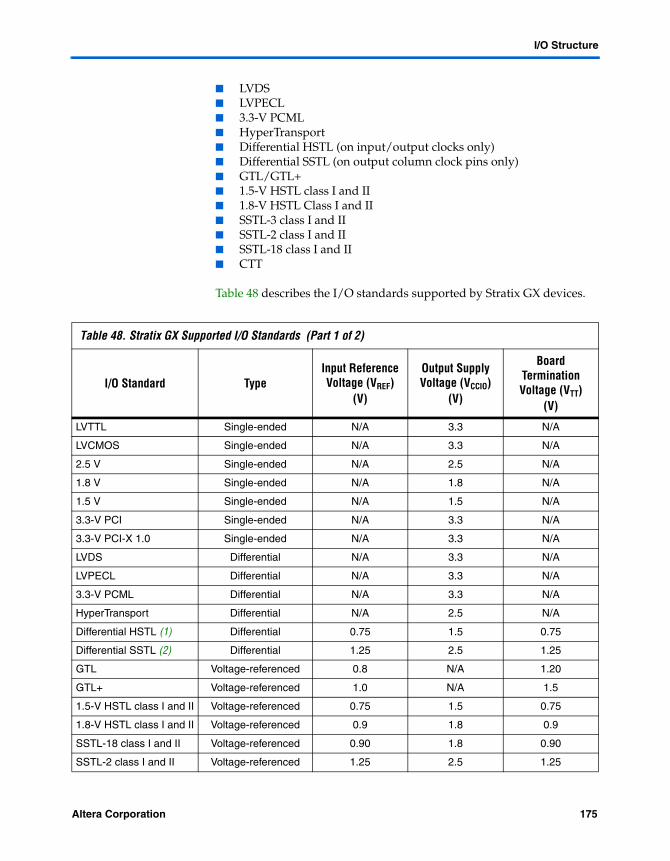
I/O Structure
LVDS LVPECL 3.3-V PCML HyperTransport Differential HSTL (on input/output clocks only) Differential SSTL (on output column clock pins only) GTL/GTL+ 1.5-V HSTL class I and II 1.8-V HSTL Class I and II SSTL-3 class I and II SSTL-2 class I and II SSTL-18 class I and II CTT
Table 48 describes the I/O standards supported by Stratix GX devices.
Table 48. Stratix GX Supported I/O Standards (Part 1 of 2)
I/O Standard TypeInput Reference Voltage (VREF)
(V)
Output Supply Voltage (VCCIO)
(V)
Board Termination Voltage (VTT)
(V)
LVTTL Single-ended N/A 3.3 N/A
LVCMOS Single-ended N/A 3.3 N/A
2.5 V Single-ended N/A 2.5 N/A
1.8 V Single-ended N/A 1.8 N/A
1.5 V Single-ended N/A 1.5 N/A
3.3-V PCI Single-ended N/A 3.3 N/A
3.3-V PCI-X 1.0 Single-ended N/A 3.3 N/A
LVDS Differential N/A 3.3 N/A
LVPECL Differential N/A 3.3 N/A
3.3-V PCML Differential N/A 3.3 N/A
HyperTransport Differential N/A 2.5 N/A
Differential HSTL (1) Differential 0.75 1.5 0.75
Differential SSTL (2) Differential 1.25 2.5 1.25
GTL Voltage-referenced 0.8 N/A 1.20
GTL+ Voltage-referenced 1.0 N/A 1.5
1.5-V HSTL class I and II Voltage-referenced 0.75 1.5 0.75
1.8-V HSTL class I and II Voltage-referenced 0.9 1.8 0.9
SSTL-18 class I and II Voltage-referenced 0.90 1.8 0.90
SSTL-2 class I and II Voltage-referenced 1.25 2.5 1.25
Altera Corporation 175Preliminary
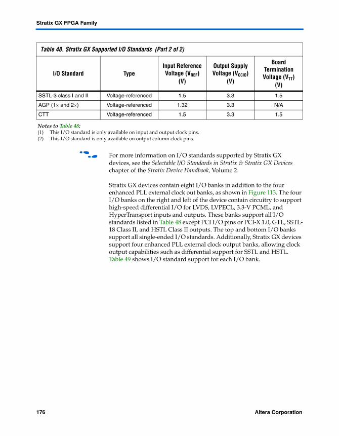
Stratix GX FPGA Family
f For more information on I/O standards supported by Stratix GX devices, see the Selectable I/O Standards in Stratix & Stratix GX Devices chapter of the Stratix Device Handbook, Volume 2.
Stratix GX devices contain eight I/O banks in addition to the four enhanced PLL external clock out banks, as shown in Figure 113. The four I/O banks on the right and left of the device contain circuitry to support high-speed differential I/O for LVDS, LVPECL, 3.3-V PCML, and HyperTransport inputs and outputs. These banks support all I/O standards listed in Table 48 except PCI I/O pins or PCI-X 1.0, GTL, SSTL-18 Class II, and HSTL Class II outputs. The top and bottom I/O banks support all single-ended I/O standards. Additionally, Stratix GX devices support four enhanced PLL external clock output banks, allowing clock output capabilities such as differential support for SSTL and HSTL. Table 49 shows I/O standard support for each I/O bank.
SSTL-3 class I and II Voltage-referenced 1.5 3.3 1.5
AGP (1× and 2×) Voltage-referenced 1.32 3.3 N/A
CTT Voltage-referenced 1.5 3.3 1.5
Notes to Table 48:(1) This I/O standard is only available on input and output clock pins.(2) This I/O standard is only available on output column clock pins.
Table 48. Stratix GX Supported I/O Standards (Part 2 of 2)
I/O Standard TypeInput Reference Voltage (VREF)
(V)
Output Supply Voltage (VCCIO)
(V)
Board Termination Voltage (VTT)
(V)
176 Altera CorporationPreliminary
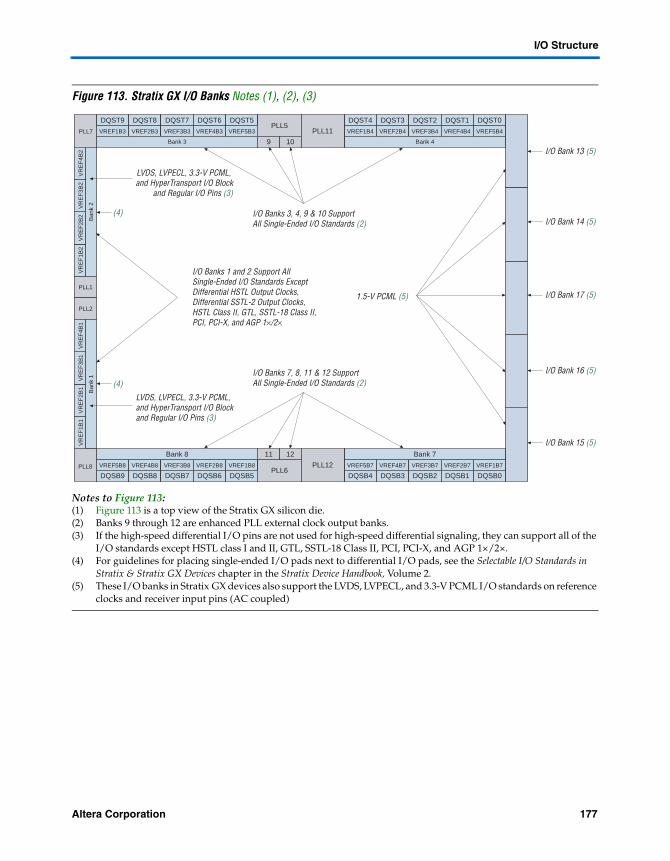
I/O Structure
Figure 113. Stratix GX I/O Banks Notes (1), (2), (3)
Notes to Figure 113:(1) Figure 113 is a top view of the Stratix GX silicon die.(2) Banks 9 through 12 are enhanced PLL external clock output banks.(3) If the high-speed differential I/O pins are not used for high-speed differential signaling, they can support all of the
I/O standards except HSTL class I and II, GTL, SSTL-18 Class II, PCI, PCI-X, and AGP 1×/2×.(4) For guidelines for placing single-ended I/O pads next to differential I/O pads, see the Selectable I/O Standards in
Stratix & Stratix GX Devices chapter in the Stratix Device Handbook, Volume 2.(5) These I/O banks in Stratix GX devices also support the LVDS, LVPECL, and 3.3-V PCML I/O standards on reference
clocks and receiver input pins (AC coupled)
LVDS, LVPECL, 3.3-V PCML, and HyperTransport I/O Blockand Regular I/O Pins (3)
I/O Banks 3, 4, 9 & 10 Support All Single-Ended I/O Standards (2)
I/O Banks 7, 8, 11 & 12 Support All Single-Ended I/O Standards (2)
I/O Banks 1 and 2 Support AllSingle-Ended I/O Standards Except Differential HSTL Output Clocks, Differential SSTL-2 Output Clocks, HSTL Class II, GTL, SSTL-18 Class II, PCI, PCI-X, and AGP 1×/2×
DQST9 DQST8 DQST7 DQST6 DQST5 DQST4 DQST3 DQST2 DQST1 DQST0PLL5
VREF1B3 VREF2B3 VREF3B3 VREF4B3 VREF5B3 VREF1B4 VREF2B4 VREF3B4 VREF4B4 VREF5B4
VREF5B8 VREF4B8 VREF3B8 VREF2B8 VREF1B8 VREF5B7 VREF4B7 VREF3B7 VREF2B7 VREF1B7PLL6
DQSB9 DQSB8 DQSB7 DQSB6 DQSB5 DQSB4 DQSB3 DQSB2 DQSB1 DQSB0
9 10
VR
EF
1B2
VR
EF
2B2
VR
EF
3B2
VR
EF
4B2
VR
EF
1B1
VR
EF
2B1
VR
EF
3B1
VR
EF
4B1
PLL1
PLL2
Ban
k 1
Ban
k 2
Bank 3 Bank 4
11 12Bank 8 Bank 7
LVDS, LVPECL, 3.3-V PCML, and HyperTransport I/O Block
and Regular I/O Pins (3)
PLL7
PLL8 PLL12
PLL11
(4)
(4)
I/O Bank 13 (5)
I/O Bank 14 (5)
I/O Bank 17 (5)
I/O Bank 16 (5)
I/O Bank 15 (5)
1.5-V PCML (5)
Altera Corporation 177Preliminary

Stratix GX FPGA Family
Table 49 shows I/O standard support for each I/O bank.
Table 49. I/O Support by Bank (Part 1 of 2)
I/O Standard Top & Bottom Banks (3, 4, 7 & 8)
Left Banks(1 & 2)
Enhanced PLL External Clock Output Banks
(9, 10, 11 & 12)
LVTTL v v v
LVCMOS v v v
2.5 V v v v
1.8 V v v v
1.5 V v v v
3.3-V PCI v v
3.3-V PCI-X 1.0 v v
LVPECL v v
3.3-V PCML v v
LVDS v v
HyperTransport technology v v
Differential HSTL (clock inputs) v v
Differential HSTL (clock outputs) v
Differential SSTL (clock outputs) v
3.3-V GTL v v
3.3-V GTL+ v v v
1.5-V HSTL class I v v v
1.5-V HSTL class II v v
1.8-V HSTL class I v v v
1.8-V HSTL class II v v
SSTL-18 class I v v v
SSTL-18 class II v v
SSTL-2 class I v v v
SSTL-2 class II v v v
SSTL-3 class I v v v
178 Altera CorporationPreliminary
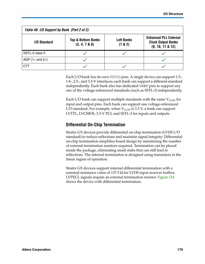
I/O Structure
Each I/O bank has its own VCCIO pins. A single device can support 1.5-, 1.8-, 2.5-, and 3.3-V interfaces; each bank can support a different standard independently. Each bank also has dedicated VREF pins to support any one of the voltage-referenced standards (such as SSTL-3) independently.
Each I/O bank can support multiple standards with the same VCCIO for input and output pins. Each bank can support one voltage-referenced I/O standard. For example, when VCCIO is 3.3 V, a bank can support LVTTL, LVCMOS, 3.3-V PCI, and SSTL-3 for inputs and outputs.
Differential On-Chip Termination
Stratix GX devices provide differential on-chip termination (LVDS I/O standard) to reduce reflections and maintain signal integrity. Differential on-chip termination simplifies board design by minimizing the number of external termination resistors required. Termination can be placed inside the package, eliminating small stubs that can still lead to reflections. The internal termination is designed using transistors in the linear region of operation.
Stratix GX devices support internal differential termination with a nominal resistance value of 137.5 Ω for LVDS input receiver buffers. LVPECL signals require an external termination resistor. Figure 114 shows the device with differential termination.
SSTL-3 class II v v v
AGP (1× and 2×) v v
CTT v v v
Table 49. I/O Support by Bank (Part 2 of 2)
I/O Standard Top & Bottom Banks (3, 4, 7 & 8)
Left Banks(1 & 2)
Enhanced PLL External Clock Output Banks
(9, 10, 11 & 12)
Altera Corporation 179Preliminary

Stratix GX FPGA Family
Figure 114. LVDS Input Differential On-Chip Termination
I/O banks on the left and right side of the device support LVDS receiver (far-end) differential termination.
Table 50 shows the Stratix GX device differential termination support.
Table 51 shows the termination support for different pin types.
The differential on-chip resistance at the receiver input buffer is 118 Ω ±20 %.
RD+
Ð
+
Ð
TransmittingDevice
Receiving Device withDifferential Termination
Z0
Z0
Table 50. Differential Termination Supported by I/O Banks
Differential Termination Support I/O Standard Support Top & Bottom Banks (3, 4, 7 & 8) Left Banks (1 & 2)
Differential termination (1), (2) LVDS v
Notes to Table 50:(1) Clock pin CLK0, CLK2, CLK9, CLK11, and pins FPLL[7..10]CLK do not support differential termination.(2) Differential termination is only supported for LVDS because of a 3.3-V VC C I O.
Table 51. Differential Termination Support Across Pin Types
Pin Type RD
Top and bottom I/O banks (3, 4, 7, and 8)
DIFFIO_RX[] v
CLK[0,2,9,11],CLK[4-7],CLK[12-15]
CLK[1,3,8,10] v
FCLK
FPLL[7..10]CLK
180 Altera CorporationPreliminary

I/O Structure
However, there is additional resistance present between the device ball and the input of the receiver buffer, as shown in Figure 1. This resistance is because of package trace resistance (which can be calculated as the resistance from the package ball to the pad) and the parasitic layout metal routing resistance (which is shown between the pad and the intersection of the on-chip termination and input buffer).
Figure 115. Differential Resistance of LVDS Differential Pin Pair (RD)
Table 52 defines the specification for internal termination resistance for commercial devices.
MultiVolt I/O Interface
The Stratix GX architecture supports the MultiVolt I/O interface feature, which allows Stratix GX devices in all packages to interface with systems of different supply voltages.
The Stratix GX VCCINT pins must always be connected to a 1.5-V power supply. With a 1.5-V VCCINT level, input pins are 1.5-V, 1.8-V, 2.5-V, and 3.3-V tolerant. The VCCIO pins can be connected to either a 1.5-V, 1.8-V,
LVDSInput Buffer
Differential On-ChipTermination Resistor
9.3 Ω
9.3 Ω
0.3 Ω
0.3 Ω
RD
PadPackage Ball
Package Ball Pad
Table 52. Differential On-Chip Termination
Symbol Description Conditions Resistance
UnitMin Typ Max
RD (2) Internal differential termination for LVDS Commercial (1), (3) 110 135 165 Ω
Industrial (2), (3) 100 135 170 Ω
Notes to Table 52:(1) Data measured over minimum conditions (Tj = 0 C, VC C I O +5%) and maximum conditions (Tj = 85 C,
VCCIO = –5%).(2) Data measured over minimum conditions (Tj = –40 C, VCCIO +5%) and maximum conditions (Tj = 100 C,
VCCIO = –5%).(3) LVDS data rate is supported for 840 Mbps using internal differential termination.
Altera Corporation 181Preliminary

Stratix GX FPGA Family
2.5-V, or 3.3-V power supply, depending on the output requirements. The output levels are compatible with systems of the same voltage as the power supply (for example, when VCCIO pins are connected to a 1.5-V power supply, the output levels are compatible with 1.5-V systems). When VCCIO pins are connected to a 3.3-V power supply, the output high is 3.3 V and is compatible with 3.3-V or 5.0-V systems.
Table 53 summarizes Stratix GX MultiVolt I/O support.
Power Sequencing & Hot Socketing
Because Stratix GX devices can be used in a mixed-voltage environment, they have been designed specifically to tolerate any possible power-up sequence. Therefore, the VCCIO and VCCINT power supplies may be powered in any order.
Signals can be driven into Stratix GX devices before and during power up without damaging the device. In addition, Stratix GX devices do not drive out during power up. Once operating conditions are reached and the device is configured, Stratix GX devices operate as specified by the user. For more information, see Hot Socketing in the Selectable I/O Standards in Stratix & Stratix GX Devices chapter in the Stratix Device Handbook, Volume 2.
Table 53. Stratix GX MultiVolt I/O Support Note (1)
VCCIO (V)Input Signal (5) Output Signal (6)
1.5 V 1.8 V 2.5 V 3.3 V 5.0 V 1.5 V 1.8 V 2.5 V 3.3 V 5.0 V
1.5 v v v (2) v (2) v
1.8 v (2) v v (2) v (2) v (3) v
2.5 v v v (3) v (3) v
3.3 v (2) v v (4) v (3) v (3) v (3) v v
Notes to Table 53:(1) To drive inputs higher than VCCIO but less than 4.1 V, disable the PCI clamping diode. However, to drive 5.0-V
inputs to the device, enable the PCI clamping diode to prevent VI from rising above 4.0 V.(2) The input pin current may be slightly higher than the typical value.(3) Although VCCIO specifies the voltage necessary for the Stratix GX device to drive out, a receiving device powered
at a different level can still interface with the Stratix GX device if it has inputs that tolerate the VCCIO value.(4) Stratix GX devices can be 5.0-V tolerant with the use of an external resistor and the internal PCI clamp diode.(5) This is the external signal that is driving the Stratix GX device.(6) This represents the system voltage that Stratix GX supports when a VCCIO pin is connected to a specific voltage
level. For example, when VCCIO is 3.3 V and if the I/O standard is LVTTL/LVCMOS, the output high of the signal coming out from Stratix GX is 3.3 V and is compatible with 3.3-V or 5.0-V systems.
182 Altera CorporationPreliminary

IEEE Std. 1149.1 (JTAG) Boundary-Scan Support
IEEE Std. 1149.1 (JTAG) Boundary-Scan Support
All Stratix GX devices provide JTAG BST circuitry that complies with the IEEE Std. 1149.1a-1990 specification. JTAG boundary-scan testing can be performed either before or after, but not during configuration. Stratix GX devices can also use the JTAG port for configuration together with either the Quartus II software or hardware using either Jam Files (.jam) or Jam Byte-Code Files (.jbc).
Stratix GX devices support IOE I/O standard setting reconfiguration through the JTAG BST chain. The JTAG chain can update the I/O standard for all input and output pins any time before or during user mode. Designers can use this ability for JTAG testing before configuration when some of the Stratix GX pins drive or receive from other devices on the board using voltage-referenced standards. Because the Stratix GX device may not be configured before JTAG testing, the I/O pins may not be configured for appropriate electrical standards for chip-to-chip communication. Programming those I/O standards via JTAG allows full designers to fully test I/O connection to other devices.
The enhanced PLL reconfiguration bits are part of the JTAG chain before configuration and after power-up. After device configuration, the PLL reconfiguration bits are not part of the JTAG chain.
Stratix GX devices also use the JTAG port to monitor the logic operation of the device with the SignalTap® embedded logic analyzer. Stratix GX devices support the JTAG instructions shown in Table 54.
Table 54. Stratix GX JTAG Instructions (Part 1 of 2)
JTAG Instruction Description
SAMPLE/PRELOAD Allows a snapshot of signals at the device pins to be captured and examined during normal device operation, and permits an initial data pattern to be output at the device pins. Also used by the SignalTap® embedded logic analyzer.
EXTEST (1) Allows the external circuitry and board-level interconnects to be tested by forcing a test pattern at the output pins and capturing test results at the input pins.
BYPASS Places the 1-bit bypass register between the TDI and TDO pins, which allows the BST data to pass synchronously through selected devices to adjacent devices during normal device operation.
USERCODE Selects the 32-bit USERCODE register and places it between the TDI and TDO pins, allowing the USERCODE to be serially shifted out of TDO.
IDCODE Selects the IDCODE register and places it between TDI and TDO, allowing the IDCODE to be serially shifted out of TDO.
HIGHZ (1) Places the 1-bit bypass register between the TDI and TDO pins, which allows the BST data to pass synchronously through selected devices to adjacent devices during normal device operation, while tri-stating all of the I/O pins.
Altera Corporation 183Preliminary
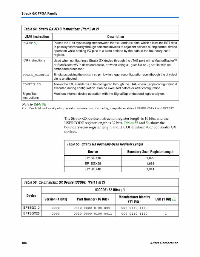
Stratix GX FPGA Family
The Stratix GX device instruction register length is 10 bits, and the USERCODE register length is 32 bits. Tables 55 and 56 show the boundary-scan register length and IDCODE information for Stratix GX devices.
CLAMP (1) Places the 1-bit bypass register between the TDI and TDO pins, which allows the BST data to pass synchronously through selected devices to adjacent devices during normal device operation while holding I/O pins to a state defined by the data in the boundary-scan register.
ICR instructions Used when configuring a Stratix GX device through the JTAG port with a MasterBlasterTM or ByteBlasterMVTM download cable, or when using a .jam file or .jbc file with an embedded processor.
PULSE_NCONFIG Emulates pulsing the nCONFIG pin low to trigger reconfiguration even though the physical pin is unaffected.
CONFIG_IO Allows the IOE standards to be configured through the JTAG chain. Stops configuration if executed during configuration. Can be executed before or after configuration.
SignalTap instructions
Monitors internal device operation with the SignalTap embedded logic analyzer.
Note to Table 54:(1) Bus hold and weak pull-up resistor features override the high-impedance state of HIGHZ, CLAMP, and EXTEST.
Table 54. Stratix GX JTAG Instructions (Part 2 of 2)
JTAG Instruction Description
Table 55. Stratix GX Boundary-Scan Register Length
Device Boundary-Scan Register Length
EP1SGX10 1,029
EP1SGX25 1,665
EP1SGX40 1,941
Table 56. 32-Bit Stratix GX Device IDCODE (Part 1 of 2)
Device
IDCODE (32 Bits) (1)
Version (4 Bits) Part Number (16 Bits) Manufacturer Identity (11 Bits) LSB (1 Bit) (2)
EP1SGX10 0000 0010 0000 0100 0001 000 0110 1110 1
EP1SGX25 0000 0010 0000 0100 0011 000 0110 1110 1
184 Altera CorporationPreliminary

IEEE Std. 1149.1 (JTAG) Boundary-Scan Support
Figure 116 shows the timing requirements for the JTAG signals.
Figure 116. Stratix GX JTAG Waveforms
Table 57 shows the JTAG timing parameters and values for Stratix GX devices.
EP1SGX40 0000 0010 0000 0100 0101 000 0110 1110 1
Notes to Table 56:(1) The most significant bit (MSB) is at the left end of the string.(2) The IDCODE’s least significant bit (LSB) is always 1.
Table 56. 32-Bit Stratix GX Device IDCODE (Part 2 of 2)
Device
IDCODE (32 Bits) (1)
Version (4 Bits) Part Number (16 Bits) Manufacturer Identity (11 Bits) LSB (1 Bit) (2)
Table 57. Stratix GX JTAG Timing Parameters & Values (Part 1 of 2)
Symbol Parameter Min (ns) Max (ns)
tJ C P TCK clock period 100
tJ C H TCK clock high time 50
tJ C L TCK clock low time 50
tJ P S U JTAG port setup time 20
TDO
TCK
tJPZX tJPCO
tJPH
t JPXZ
tJCP
tJPSU t JCL tJCH
TDI
TMS
Signalto Be
Captured
Signalto Be
Driven
tJSZX
tJSSU tJSH
tJSCO tJSXZ
Altera Corporation 185Preliminary

Stratix GX FPGA Family
f For more information on JTAG, see the following documents:
AN 39: IEEE Std. 1149.1 (JTAG) Boundary-Scan Testing in Altera Devices Jam Programming & Test Language Specification
SignalTap Embedded Logic Analyzer
Stratix GX devices feature the SignalTap embedded logic analyzer, which monitors design operation over a period of time through the IEEE Std. 1149.1 (JTAG) circuitry. A designer can analyze internal logic at speed without bringing internal signals to the I/O pins. This feature is particularly important for advanced packages, such as FineLine BGA packages, because it can be difficult to add a connection to a pin during the debugging process after a board is designed and manufactured.
Configuration The logic, circuitry, and interconnects in the Stratix GX architecture are configured with CMOS SRAM elements. Stratix GX devices are reconfigurable and are 100% tested prior to shipment. As a result, the designer does not have to generate test vectors for fault coverage purposes, and can instead focus on simulation and design verification. In addition, the designer does not need to manage inventories of different ASIC designs. Stratix GX devices can be configured on the board for the specific functionality required.
Stratix GX devices are configured at system power-up with data stored in an Altera serial configuration device or provided by a system controller. Altera offers in-system programmability (ISP)-capable configuration devices that configure Stratix GX devices via a serial data stream. Stratix GX devices can be configured in under 100 ms using 8-bit parallel data at 100 MHz. The Stratix GX device’s optimized interface allows microprocessors to configure it serially or in parallel, and synchronously
tJ P H JTAG port hold time 45
tJ P CO JTAG port clock to output 25
tJ P Z X JTAG port high impedance to valid output 25
tJ P X Z JTAG port valid output to high impedance 25
tJ S S U Capture register setup time 20
tJ S H Capture register hold time 45
tJ S CO Update register clock to output 35
tJ S Z X Update register high impedance to valid output 35
tJ S X Z Update register valid output to high impedance 35
Table 57. Stratix GX JTAG Timing Parameters & Values (Part 2 of 2)
Symbol Parameter Min (ns) Max (ns)
186 Altera CorporationPreliminary

Configuration
or asynchronously. The interface also enables microprocessors to treat Stratix GX devices as memory and configure them by writing to a virtual memory location, making reconfiguration easy. After a Stratix GX device has been configured, it can be reconfigured in-circuit by resetting the device and loading new data. Real-time changes can be made during system operation, enabling innovative reconfigurable computing applications.
Operating Modes
The Stratix GX architecture uses SRAM configuration elements that require configuration data to be loaded each time the circuit powers up. The process of physically loading the SRAM data into the device is called configuration. During initialization, which occurs immediately after configuration, the device resets registers, enables I/O pins, and begins to operate as a logic device. The I/O pins are tri-stated during power up, and before and during configuration. Together, the configuration and initialization processes are called command mode. Normal device operation is called user mode.
A built-in weak pull-up resistor pulls all user I/O pins to VCCIO before and during device configuration.
SRAM configuration elements allow Stratix GX devices to be reconfigured in-circuit by loading new configuration data into the device. With real-time reconfiguration, the device is forced into command mode with a device pin. The configuration process loads different configuration data, reinitializes the device, and resumes user-mode operation. Designers can perform in-field upgrades by distributing new configuration files either within the system or remotely.
Configuration Schemes
Designers can load the configuration data for a Stratix GX device with one of five configuration schemes (see Table 58), chosen on the basis of the target application. Designers can use a configuration device, intelligent controller, or the JTAG port to configure a Stratix GX device. A configuration device can automatically configure a Stratix GX device at system power-up.
Altera Corporation 187Preliminary

Stratix GX FPGA Family
Multiple Stratix GX devices can be configured in any of five configuration schemes by connecting the configuration enable (nCE) and configuration enable output (nCEO) pins on each device.
Partial Reconfiguration
The enhanced PLLs within the Stratix GX device family support partial reconfiguration of their multiply, divide, and time delay settings without reconfiguring the entire device. Designers can use either serial data from the logic array or regular I/O pins to program the PLL’s counter settings in a serial chain. This option provides considerable flexibility for frequency synthesis, allowing real-time variation of the PLL frequency and delay. The rest of the device is functional while reconfiguring the PLL. See “Enhanced PLLs” on page 143 for more information on Stratix GX PLLs.
Remote Update Configuration Modes
Stratix GX devices also support remote configuration using an Altera enhanced configuration device (for example, EPC16, EPC8, and EPC4 devices) with page mode selection. Factory configuration data is stored in the default page of the configuration device. This is the default configuration which contains the design required to control remote updates and handle or recover from errors. The designer writes the factory configuration once into the flash memory or configuration device. Remote update data can update any of the remaining pages of the configuration device. If there is an error or corruption in a remote update configuration, the configuration device reverts back to the factory configuration information.
Table 58. Data Sources for Configuration
Configuration Scheme Data Source
Configuration device Enhanced or EPC2 configuration device
Passive serial (PS) ByteBlasterMV or MasterBlaster download cable or serial data source
Passive parallel asynchronous (PPA)
Parallel data source
Fast passive parallel Parallel data source
JTAG MasterBlaster or ByteBlasterMV download cable or a microprocessor with a Jam or JBC file (.jam or .jbc)
188 Altera CorporationPreliminary
Configuration
There are two remote configuration modes: remote and local configuration. Designers can use the remote update configuration mode for all three configuration modes: serial, parallel synchronous, and parallel asynchronous. Configuration devices (for example, EPC16 devices) only support serial and parallel synchronous modes. Asynchronous parallel mode allows remote updates when an intelligent host is used to configure the Stratix GX device. This host must support page mode settings similar to an EPC16 device.
Remote Update Mode
When the Stratix GX device is first powered-up in remote update programming mode, it loads the configuration located at page address 000. The factory configuration should always be located at page address 000, and should never be remotely updated. The factory configuration contains the required logic to perform the following operations:
Determine the page address/load location for the next application’s configuration data
Recover from a previous configuration error Receive new configuration data and write it into the configuration
device
The factory configuration is the default and takes control if an error occurs while loading the application configuration.
While in the factory configuration, the factory-configuration logic performs the following operations:
Loads a remote update-control register to determine the page address of the new application configuration
Determines whether to enable a user watchdog timer for the application configuration
Determines what the watchdog timer setting should be if it is enabled
The user watchdog timer is a counter that must be continually reset within a specific amount of time in the user mode of an application configuration to ensure that valid configuration occurred during a remote update. Only valid application configurations designed for remote update can reset the user watchdog timer in user mode. If a valid application configuration does not reset the user watchdog timer in a specific amount of time, the timer updates a status register and loads the factory configuration. The user watchdog timer is automatically disabled for factory configurations.
Altera Corporation 189Preliminary
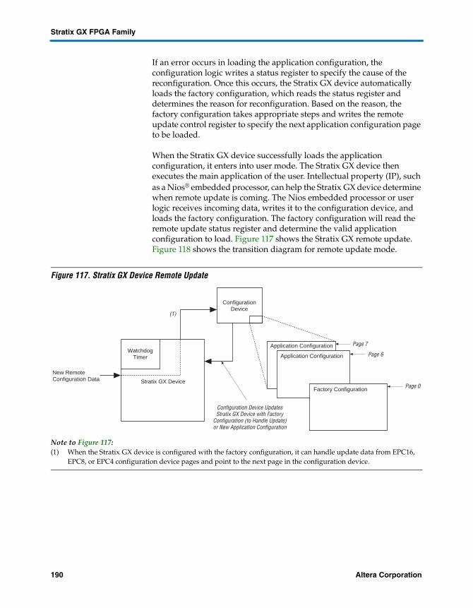
Stratix GX FPGA Family
If an error occurs in loading the application configuration, the configuration logic writes a status register to specify the cause of the reconfiguration. Once this occurs, the Stratix GX device automatically loads the factory configuration, which reads the status register and determines the reason for reconfiguration. Based on the reason, the factory configuration takes appropriate steps and writes the remote update control register to specify the next application configuration page to be loaded.
When the Stratix GX device successfully loads the application configuration, it enters into user mode. The Stratix GX device then executes the main application of the user. Intellectual property (IP), such as a Nios® embedded processor, can help the Stratix GX device determine when remote update is coming. The Nios embedded processor or user logic receives incoming data, writes it to the configuration device, and loads the factory configuration. The factory configuration will read the remote update status register and determine the valid application configuration to load. Figure 117 shows the Stratix GX remote update. Figure 118 shows the transition diagram for remote update mode.
Figure 117. Stratix GX Device Remote Update
Note to Figure 117:(1) When the Stratix GX device is configured with the factory configuration, it can handle update data from EPC16,
EPC8, or EPC4 configuration device pages and point to the next page in the configuration device.
WatchdogTimer
Stratix GX Device
New RemoteConfiguration Data
ConfigurationDevice
Application Configuration
Application Configuration
Factory Configuration
(1)
Configuration Device UpdatesStratix GX Device with Factory
Configuration (to Handle Update)or New Application Configuration
Page 7
Page 6
Page 0
190 Altera CorporationPreliminary

Configuration
Figure 118. Remote Update Transition Diagram Notes (1), (2)
Notes to Figure 118:(1) Remote update of application configuration is controlled by a Nios embedded processor or user logic programmed
in the factory or application configurations.(2) Up to seven pages can be specified allowing up to seven different configuration applications.
ConfigurationError
ConfigurationError
Application 1Configuration
ConfigurationError
FactoryConfiguration
Reload anApplication
Reload anApplication
Application nConfiguration
Power-Up
Altera Corporation 191Preliminary

Stratix GX FPGA Family
Local Update Mode
Local update mode is a simplified version of the remote update. This feature is intended for simple systems that need to load a single application configuration immediately upon power-up without loading the factory configuration first. Local update designs have only one application configuration to load, so it does not require a factory configuration to determine which application configuration to use. Figure 119 shows the transition diagram for local update mode.
Figure 119. Local Update Transition Diagram
Stratix GX Automated Single Event Upset (SEU) Detection
Stratix GX devices offer on-chip circuitry for automated checking of single event upset (SEU) detection. Some applications that require the device to operate error free at high elevations or in close proximity to earth’s North or South Pole will require periodic checks to ensure continued data integrity. The error detection cyclic redundancy code (CRC) feature controlled by the Device & Pin Options dialog box in the Quartus II software uses a 32-bit CRC circuit to ensure data reliability and is one of the best options for mitigating SEU.
nCONFIG
nCONFIGConfigurationError
ApplicationConfiguration
ConfigurationError
FactoryConfiguration
Power-Upor nCONFIG
192 Altera CorporationPreliminary

Temperature-Sensing Diode
Designers can implement the error detection CRC feature with existing circuitry in Stratix GX devices, eliminating the need for external logic. For Stratix GX devices, the CRC is computed by Quartus II and downloaded into the device as a part of the configuration bit stream. The CRC_ERROR pin reports a soft error when configuration SRAM data is corrupted, triggering device reconfiguration.
Custom-Built Circuitry
Dedicated circuitry is built into Stratix GX devices to perform error detection automatically. This error detection circuitry constantly checks for errors in the configuration SRAM cells while the device is in user mode. Designers can monitor one external pin for the error and use it to trigger a reconfiguration cycle. Designers can select the desired time between checks by adjusting a built-in clock divider.
Software Interface
In the Quartus II software version 4.1 and later, designers can turn on the automated error detection CRC feature in the Device & Pin Options dialog box. This dialog box allows designers to enable the feature and set the internal frequency of the CRC between 400 kHz to 100 MHz. This controls the rate that the CRC circuitry verifies the internal configuration SRAM bits in the FPGA device.
For more information on CRC, refer to AN 357: Error Detection Using CRC in Altera FPGA Devices.
Temperature-Sensing Diode
Stratix GX devices include a diode-connected transistor for use as a temperature sensor in power management. This diode is used with an external digital thermometer device such as a MAX1617A or MAX1619 from MAXIM Integrated Products. These devices steer bias current through the Stratix GX diode, measuring forward voltage and converting this reading to temperature in the form of an 8-bit signed number (7 bits plus sign). The external device’s output represents the package temperature of the Stratix GX device and can be used for intelligent power management.
The diode requires two pins (tempdiodep and tempdioden) on the Stratix GX device to connect to the external temperature-sensing device, as shown in Figure 120. The temperature-sensing diode is a passive element and therefore can be used before the Stratix GX device is powered.
Altera Corporation 193Preliminary

Stratix GX FPGA Family
Figure 120. External Temperature-Sensing Diode
Table 59 shows the specifications for bias voltage and current of the Stratix GX temperature-sensing diode.
The temperature-sensing diode works for the entire operating range shown in Figure 121.
Table 59. Temperature-Sensing Diode Electrical Characteristics
Parameter Minimum Typical Maximum Units
IB I A S high 80 100 120 µA
IB I A S low 8 10 12 µA
VB P – VB N 0.3 0.9 V
VB N 0.7 V
Series resistance 3 W
Stratix GX Device
Temperature-Sensing Device
tempdiodep
tempdioden
194 Altera CorporationPreliminary
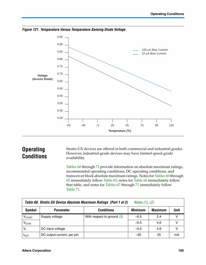
Operating Conditions
Figure 121. Temperature Versus Temperature-Sensing Diode Voltage
Operating Conditions
Stratix GX devices are offered in both commercial and industrial grades. However, industrial-grade devices may have limited speed-grade availability.
Tables 60 through 71 provide information on absolute maximum ratings, recommended operating conditions, DC operating conditions, and transceiver block absolute maximum ratings. Notes for Tables 60 through 65 immediately follow Table 65, notes for Table 66 immediately follow that table, and notes for Tables 67 through 71 immediately follow Table 71.
0.90
0.85
0.95
0.75
0.65
Voltage(Across Diode)
Temperature ( C)
0.55
0.45
0.60
0.50
0.40
0.70
0.80
–55 –30 –5 20 45 70 95 120
10 µA Bias Current100 µA Bias Current
Table 60. Stratix GX Device Absolute Maximum Ratings (Part 1 of 2) Notes (1), (2)
Symbol Parameter Conditions Minimum Maximum Unit
VCCINT Supply voltage With respect to ground (3) –0.5 2.4 V
VCCIO –0.5 4.6 V
VI DC input voltage –0.5 4.6 V
IOUT DC output current, per pin –25 25 mA
Altera Corporation 195Preliminary

Stratix GX FPGA Family
TSTG Storage temperature No bias –65 150 ° C
TAMB Ambient temperature Under bias –65 135 ° C
TJ Junction temperature BGA packages under bias 135 ° C
Table 61. Stratix GX Device Recommended Operating Conditions Note (7), (12), (13)
Symbol Parameter Conditions Minimum Maximum Unit
VCCINT Supply voltage for internal logic and input buffers
(4) 1.425 1.575 V
VCCIO Supply voltage for output buffers, 3.3-V operation
(4), (5) 3.00 (3.135) 3.60 (3.465) V
Supply voltage for output buffers, 2.5-V operation
(4) 2.375 2.625 V
Supply voltage for output buffers, 1.8-V operation
(4) 1.71 1.89 V
Supply voltage for output buffers, 1.5-V operation
(4) 1.4 1.6 V
VI Input voltage (3), (6) –0.5 4.1 V
VO Output voltage 0 VCCIO V
TJ Operating junction temperature For commercial use
0 85 ° C
For industrial use –40 100 ° C
Table 62. Stratix GX Device DC Operating Conditions Note (12)
Symbol Parameter Conditions Minimum Typical Maximum Unit
II Input pin leakage current
VI = VC C I O m a x to 0 V (8)
–10 10 µA
IOZ Tri-stated I/O pin leakage current
VO = VC CI O m a x to 0 V (8)
–10 10 µA
RCONF Value of I/O pin pull-up resistor before and during configuration
VCCIO = 3.0 V (9) 20 50 kΩ
VCCIO = 2.375 V (9) 30 80 kΩ
VCCIO = 1.71 V (9) 60 150 kΩ
Table 60. Stratix GX Device Absolute Maximum Ratings (Part 2 of 2) Notes (1), (2)
Symbol Parameter Conditions Minimum Maximum Unit
196 Altera CorporationPreliminary

Operating Conditions
Table 63. Stratix GX Transceiver Block Absolute Maximum Ratings
Symbol Parameter Conditions Minimum Maximum Units
VCC A Transceiver block supply voltage
Commercial and industrial
–0.5 4.6 V
VCC P Transceiver block supply voltage
Commercial and industrial
–0.5 2.4 V
VCC R Transceiver block supply Voltage
Commercial and industrial
–0.5 2.4 V
VCC T Transceiver block supply voltage
Commercial and industrial
–0.5 2.4 V
VCC G Transceiver block supply voltage
Commercial and industrial
–0.5 2.4 V
Receiver input voltage
VI C M ±VO D single / 2 Commercial and industrial
1.675 (10), (13)
V
refclkb input voltage
VI C M ±VO D single / 2 Commercial and industrial
1.675 (10), (13)
V
Table 64. Stratix GX Transceiver Block Operating Conditions (Part 1 of 2)
Symbol Parameter Conditions Minimum Typical Maximum Units
VCC A Transceiver block supply voltage
Commercial and industrial
3.135 3.3 3.465 V
VCC P Transceiver block supply voltage
Commercial and industrial
1.425 1.5 1.575 V
VCC R Transceiver block supply voltage
Commercial and industrial
1.425 1.5 1.575 V
VCC T Transceiver block supply voltage
Commercial and industrial
1.425 1.5 1.575 V
VCC G Transceiver block supply voltage
Commercial and industrial
1.425 1.5 1.575 V
VI D (differential p-p)
Receiver input differential voltage swing
Commercial and industrial
170 2,000 mV
refclkb input differential voltage swing
Commercial and industrial
400 2,000 mV
VI C M Receiver input common mode voltage
Commercial and industrial
1,025 1,100 1,175 V
VO D
(differential p-p)Transmitter output differential voltage
Commercial and industrial
350 1,600 mV
Altera Corporation 197Preliminary

Stratix GX FPGA Family
VO C M Transmitter output common mode voltage
Commercial and industrial
750 mV
RR E F (11) Reference resistor Commercial and industrial
2K –1% 2K 2K +1% Ω
Table 65. Stratix GX Transceiver Block On-Chip Termination
Symbol Parameter Conditions Min Typ Max Units
Rx Receiver termination Commercial and industrial, 100-Ω setting 103 108 113 Ω
Commercial and industrial, 120-Ω setting 120 128 134 Ω
Commercial and industrial, 150-Ω setting 149 158 167 Ω
Tx Transmitter termination Commercial and industrial, 100-Ω setting 103 108 113 Ω
Commercial and industrial, 120-Ω setting 120 128 134 Ω
Commercial and industrial, 150-Ω setting 149 158 167 Ω
Refclkb Dedicated transceiver clock termination
Commercial and industrial, 100-Ω setting 103 108 113 Ω
Commercial and industrial, 120-Ω setting 120 128 134 Ω
Commercial and industrial, 150-Ω setting 149 158 167 Ω
Notes to Tables 60 through 65:(1) See the Operating Requirements for Altera Devices Data Sheet.(2) Conditions beyond those listed in Table 60 may cause permanent damage to a device. Additionally, device
operation at the absolute maximum ratings for extended periods of time may have adverse affects on the device.(3) Minimum DC input is –0.5 V. During transitions, the inputs may undershoot to –0.5 V or overshoot to 4.6 V for
input currents less than 100 mA and periods shorter than 20 ns. (The information in this note does not include the transceiver pins. See note 13 for information about the transient voltage on the transceiver pins.)
(4) Maximum VCC rise time is 100 ms, and VCC must rise monotonically.(5) VCCIO maximum and minimum conditions for LVPECL, LVDS, and 3.3-V PCML are shown in parentheses.(6) All pins, including dedicated inputs, clock, I/O, and JTAG pins, may be driven before VCCINT and VCCIO are
powered.(7) Typical values are for TA = 25° C, VCCINT = 1.5 V, and VCCIO = 1.5 V, 1.8 V, 2.5 V, and 3.3 V.(8) This value is specified for normal device operation. The value may vary during power-up. This applies for all VCCIO
settings (3.3, 2.5, 1.8, and 1.5 V).(9) Pin pull-up resistance values will lower if an external source drives the pin higher than VCCIO.(10) The device can tolerate prolonged operation at this absolute maximum, as long as the maximum specification is
not violated.(11) The DC signal on this pin must be as clean as possible. Ensure that no noise is coupled to this pin.(12) The Stratix GX device’s recommended operating conditions do not include the transceiver. Refer to Tables 63 to 66.(13) Minimum DC input to the transceiver pins is –0.5 V. During transitions, the transceiver pins may undershoot to
–0.5 V or overshoot to 3.5 V for input currents less than 100 mA and periods shorter than 20 ns.
Table 64. Stratix GX Transceiver Block Operating Conditions (Part 2 of 2)
Symbol Parameter Conditions Minimum Typical Maximum Units
198 Altera CorporationPreliminary

Operating Conditions
Table 66. Stratix GX Transceiver Block AC Specification (Part 1 of 3)
Symbol / Description Conditions
-5 Commercial Speed Grade (5)
-6 Commercial & Industrial Speed
Grade(5)
-7 Commercial & Industrial Speed
Grade(5)
Unit
Min Typ Max Min Typ Max Min Typ Max
Power per quadrant (PCS + PMA)
3.125 Gbps, 400-mV Vo d
0 pre-emphasis
450 450 mW
Dedicated Reference Clock
REFCLK Jitter tolerance (peak-to-peak)
Jitter components <20 MHz
20 20 20 ps
Wideband 50 50 50 ps
REFCLK (reference input clock frequency)– dedicated refclkb pins
25 650 25 650 25 312.5 MHz
REFCLK (reference input clock frequency)– PLD clock resources
25 325 25 325 25 156.25 MHz
Receiver
Serial data rate (general)
Commercial / industrial
614 3,187.5 614 3,187.5 614 2,500 Mbps
Serial data rate (8B/10B encoded)
Commercial / industrial
500 3,187.5 500 3,187.5 500 2,500 Mbps
Parallel transceiver/logic array interface speed
20 398.4 20 375 20 312.5 MHz
Rate matching frequency tolerance
XAUI mode only
±100 ±100 ±100 ppm
Receiver total jitter tolerance
@ 3.125 Gbps
0.65 0.65 UI
Altera Corporation 199Preliminary
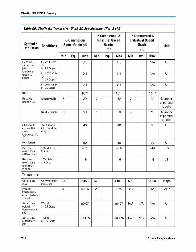
Stratix GX FPGA Family
Receive sinusoidal jitter tolerance (peak-to-peak)
f = 22.1 Khz @ 3.125 Gbps
8.5 8.5 N/A UI
f = 1.875 MHz @ 3.125 Gbps
0.1 0.1 N/A UI
f = 20 MHz @ 3.125 Gbps
0.1 0.1 N/A UI
BER 10-12 10-12 10-12
Receive latency (2)
Single width 7 32 7 32 7 32 Number of parallel
clocks
Double width 5 19 5 19 5 19 Number of parallel
clocks
Channel to channel bit skew tolerance (4), (7)
XAUI mode / inter quadrant only
40 40 40 UI
Run-length 80 80 80 UI
Receiver return loss (differential)
100 MHz to 2.5 Ghz
–10 –10 –10 dB
Receiver return loss (common mode)
100 MHz to 2.5 Ghz
–6 –6 –6 dB
Transmitter
Serial data rate
Commercial / industrial
500 3,187.5 500 3,187.5 500 2500 Mbps
Parallel transceiver/core interface speed
20 398.4 20 375 20 312.5 MHz
Serial data output deterministic jitter
TDJ @ 3.125 Gbps
±0.07 ±0.07 N/A N/A N/A UI
Serial data output total jitter
TTJ @ 3.125 Gbps
±0.175 ±0.175 N/A N/A N/A UI
Table 66. Stratix GX Transceiver Block AC Specification (Part 2 of 3)
Symbol / Description Conditions
-5 Commercial Speed Grade (5)
-6 Commercial & Industrial Speed
Grade(5)
-7 Commercial & Industrial Speed
Grade(5)
Unit
Min Typ Max Min Typ Max Min Typ Max
200 Altera CorporationPreliminary
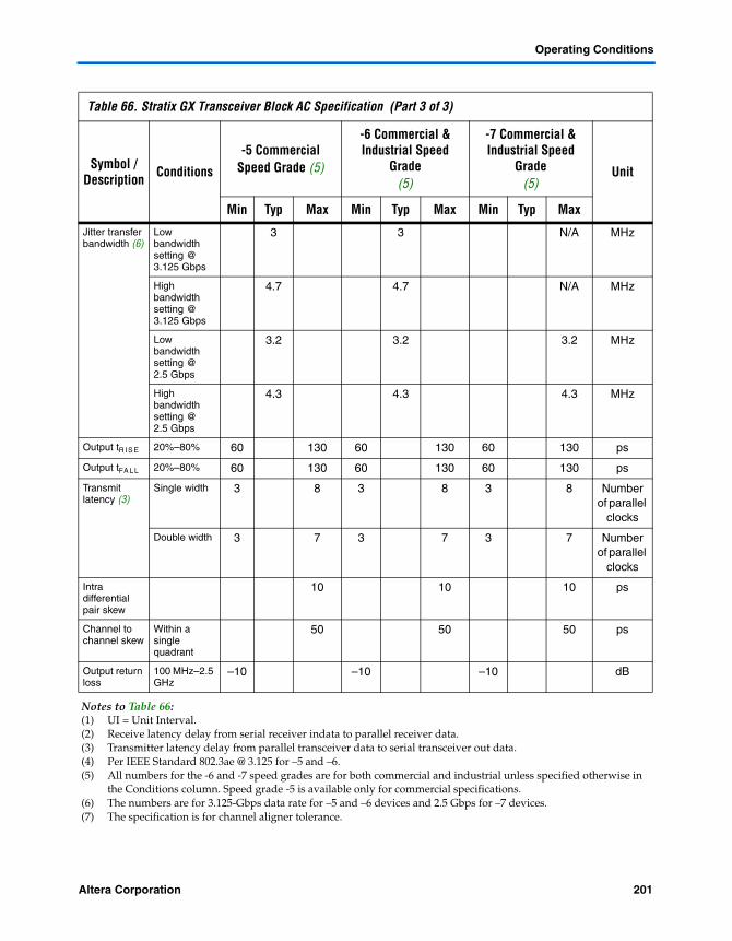
Operating Conditions
Jitter transfer bandwidth (6)
Low bandwidth setting @ 3.125 Gbps
3 3 N/A MHz
High bandwidth setting @ 3.125 Gbps
4.7 4.7 N/A MHz
Low bandwidth setting @ 2.5 Gbps
3.2 3.2 3.2 MHz
High bandwidth setting @ 2.5 Gbps
4.3 4.3 4.3 MHz
Output tR I S E 20%–80% 60 130 60 130 60 130 ps
Output tFA L L 20%–80% 60 130 60 130 60 130 ps
Transmit latency (3)
Single width 3 8 3 8 3 8 Number of parallel
clocks
Double width 3 7 3 7 3 7 Number of parallel
clocks
Intra differential pair skew
10 10 10 ps
Channel to channel skew
Within a single quadrant
50 50 50 ps
Output return loss
100 MHz–2.5 GHz
–10 –10 –10 dB
Notes to Table 66:(1) UI = Unit Interval.(2) Receive latency delay from serial receiver indata to parallel receiver data.(3) Transmitter latency delay from parallel transceiver data to serial transceiver out data.(4) Per IEEE Standard 802.3ae @ 3.125 for –5 and –6.(5) All numbers for the -6 and -7 speed grades are for both commercial and industrial unless specified otherwise in
the Conditions column. Speed grade -5 is available only for commercial specifications.(6) The numbers are for 3.125-Gbps data rate for –5 and –6 devices and 2.5 Gbps for –7 devices.(7) The specification is for channel aligner tolerance.
Table 66. Stratix GX Transceiver Block AC Specification (Part 3 of 3)
Symbol / Description Conditions
-5 Commercial Speed Grade (5)
-6 Commercial & Industrial Speed
Grade(5)
-7 Commercial & Industrial Speed
Grade(5)
Unit
Min Typ Max Min Typ Max Min Typ Max
Altera Corporation 201Preliminary

Stratix GX FPGA Family
Table 67. LVTTL Specifications
Symbol Parameter Conditions Minimum Maximum Units
VCCIO Output supply voltage 3.0 3.6 V
VI H High-level input voltage 1.7 4.1 V
VIL Low-level input voltage –0.5 0.7 V
VOH High-level output voltage IOH = –4 to –24 mA (1) 2.4 V
VOL Low-level output voltage IOL = 4 to 24 mA (1) 0.45 V
Table 68. LVCMOS Specifications
Symbol Parameter Conditions Minimum Maximum Units
VCCIO Output supply voltage 3.0 3.6 V
VIH High-level input voltage 1.7 4.1 V
VIL Low-level input voltage –0.5 0.7 V
VOH High-level output voltage VCCIO = 3.0, IOH = –0.1 mA
VCCIO – 0.2 V
VOL Low-level output voltage VCCIO = 3.0,IOL = 0.1 mA
0.2 V
Table 69. 2.5-V I/O Specifications Note (1)
Symbol Parameter Conditions Minimum Maximum Units
VCCIO Output supply voltage 2.375 2.625 V
VIH High-level input voltage 1.7 4.1 V
VIL Low-level input voltage –0.5 0.7 V
VOH High-level output voltage IOH = –0.1 mA 2.1 V
IOH = –1 mA 2.0 V
IOH = –2 to –16 mA (1) 1.7 V
VOL Low-level output voltage IOL = 0.1 mA 0.2 V
IOH = 1 mA 0.4 V
IOH = 2 to 16 mA (1) 0.7 V
202 Altera CorporationPreliminary

Operating Conditions
Figures 122 and 123 show receiver input and transmitter output waveforms, respectively, for all differential I/O standards (LVDS, 3.3-V PCML, LVPECL, and HyperTransport technology).
Table 70. 1.8-V I/O Specifications
Symbol Parameter Conditions Minimum Maximum Units
VCCIO Output supply voltage 1.65 1.95 V
VI H High-level input voltage 0.65 × VCCIO 2.25 V
VIL Low-level input voltage –0.3 0.35 × VCCIO V
VOH High-level output voltage IOH = –2 to –8 mA (1) VCCIO – 0.45 V
VOL Low-level output voltage IOL = 2 to 8 mA (1) 0.45 V
Table 71. 1.5-V I/O Specifications
Symbol Parameter Conditions Minimum Maximum Units
VCCIO Output supply voltage 1.4 1.6 V
VI H High-level input voltage 0.65 × VCCIO VCCIO + 0.3 V
VIL Low-level input voltage –0.3 0.35 × VCCIO V
VOH High-level output voltage IOH = –2 mA (1) 0.75 × VCCIO V
VOL Low-level output voltage IOL = 2 mA (1) 0.25 × VCCIO V
Note to Tables 67 through 71:(1) Drive strength is programmable according to values in Table 45 on page 172.
Altera Corporation 203Preliminary
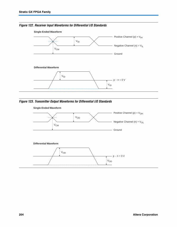
Stratix GX FPGA Family
Figure 122. Receiver Input Waveforms for Differential I/O Standards
Figure 123. Transmitter Output Waveforms for Differential I/O Standards
Single-Ended Waveform
Differential Waveform
Positive Channel (p) = VIH
Negative Channel (n) = VIL
Ground
VID
VID
VID
VCM
p − n = 0 V
Single-Ended Waveform
Differential Waveform
Positive Channel (p) = VOH
Negative Channel (n) = VOL
Ground
VOD
VOD
VOD
p − n = 0 V
VCM
204 Altera CorporationPreliminary
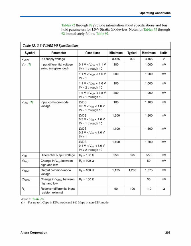
Operating Conditions
Tables 72 through 92 provide information about specifications and bus hold parameters for 1.5-V Stratix GX devices. Notes for Tables 73 through 92 immediately follow Table 92.
Table 72. 3.3-V LVDS I/O Specifications
Symbol Parameter Conditions Minimum Typical Maximum Units
VCCIO I/O supply voltage 3.135 3.3 3.465 V
VI D (1) Input differential voltage swing (single-ended)
0.1 V < VC M < 1.1 V W = 1 through 10
300 1,000 mV
1.1 V < VC M < 1.6 V W = 1
200 1,000 mV
1.1 V < VC M < 1.6 V W = 2 through 10
100 1,000 mV
1.6 V < VC M < 1.8 V W = 1 through 10
300 1,000 mV
VI C M (1) Input common-mode voltage
LVDS0.3 V < VI D < 1.0 VW = 1 through 10
100 1,100 mV
LVDS0.3 V < VI D < 1.0 VW = 1 through 10
1,600 1,800 mV
LVDS0.2 V < VI D < 1.0 VW = 1
1,100 1,600 mV
LVDS0.1 V < VI D < 1.0 VW = 2 through 10
1,100 1,600 mV
VOD Differential output voltage RL = 100 Ω 250 375 550 mV
∆VOD Change in VOD between high and low
RL = 100 Ω 50 mV
VOCM Output common-mode voltage
RL = 100 Ω 1,125 1,200 1,375 mV
∆VOCM Change in VOCM between high and low
RL = 100 Ω 50 mV
RL Receiver differential input resistor, external
90 100 110 Ω
Note to Table 72:(1) For up to 1 Gbps in DPA mode and 840 Mbps in non-DPA mode
Altera Corporation 205Preliminary

Stratix GX FPGA Family
Table 73. 3.3-V PCML Specifications
Symbol Parameter Conditions Minimum Typical Maximum Units
VCCIO I/O supply voltage 3.135 3.3 3.465 V
VID Input differential voltage swing (single-ended)
300 600 mV
VICM Input common mode voltage
1.5 3.465 V
VOD Output differential voltage (single-ended)
300 370 500 mV
∆VOD Change in VO D between high and low
50 mV
VO C M Output common mode voltage
2.5 2.85 3.3 V
∆VO C M Change in VO C M between high and low
50 mV
VT Output termination voltage VC C I O V
R1 Output external pull-up resistors
45 50 55 W
R2 Output external pull-up resistors
45 50 55 W
Table 74. LVPECL Specifications
Symbol Parameter Conditions Minimum Typical Maximum Units
VCCIO I/O supply voltage 3.135 3.3 3.465 V
VID Input differential voltage swing (single-ended)
300 1,000 mV
VICM Input common mode voltage
1 2 V
VOD Differential output voltage RL = 100 Ω 525 700 970 mV
VO C M Output common mode voltage
RL = 100 Ω 1.5 1.7 1.9 mV
RL Receiver differential input resistor, external
90 100 110 W
206 Altera CorporationPreliminary

Operating Conditions
Table 75. HyperTransport Specifications
Symbol Parameter Conditions Minimum Typical Maximum Units
VCCIO I/O supply voltage 2.375 2.5 2.625 V
VOD Differential output voltage RL = 100 Ω 380 485 820 mV
∆VO D Change in between high and low
RL = 100 Ω 50 mV
VOCM Output common mode voltage
RL = 100 Ω 440 650 780 mV
∆VO C M Change in between high and low
RL = 100 Ω 50 mV
VID Differential input voltage swing (single-ended)
300 900 mV
VICM Input common mode voltage
300 900 mV
RL Receiver differential input resistor, external
90 100 110 W
Table 76. 3.3-V PCI Specifications
Symbol Parameter Conditions Minimum Typical Maximum Units
VCCIO Output supply voltage 3.0 3.3 3.6 V
VIH High-level input voltage 0.5 × VCCIO
VCCIO + 0.5
V
VIL Low-level input voltage –0.5 0.3 × VCCIO
V
VOH High-level output voltage IOUT = –500 µA 0.9 × VCCIO
V
VOL Low-level output voltage IOUT = 1,500 µA 0.1 × VCCIO
V
Table 77. PCI-X Specifications (Part 1 of 2)
Symbol Parameter Conditions Minimum Typical Maximum Units
VCCIO Output supply voltage 3.0 3.6 V
VIH High-level input voltage 0.5 × VCCIO
VCCIO + 0.5
V
VIL Low-level input voltage –0.5 0.35 × VCCIO
V
VIPU Input pull-up voltage 0.7 × VCCIO
V
Altera Corporation 207Preliminary

Stratix GX FPGA Family
VO H High-level output voltage IO U T = –500 µA 0.9 × VC CI O
V
VO L Low-level output voltage IO U T = 1,500 µA 0.1 × VC C I O
V
Table 78. GTL+ I/O Specifications
Symbol Parameter Conditions Minimum Typical Maximum Units
VTT Termination voltage 1.35 1.5 1.65 V
VREF Reference voltage 0.88 1.0 1.12 V
VIH High-level input voltage VREF + 0.1 V
VIL Low-level input voltage VRE F – 0.1
V
VOL Low-level output voltage IOL = 36 mA (1) 0.65 V
Table 79. GTL I/O Specifications
Symbol Parameter Conditions Minimum Typical Maximum Units
VTT Termination voltage 1.14 1.2 1.26 V
VREF Reference voltage 0.74 0.8 0.86 V
VIH High-level input voltage VREF + 0.05
V
VIL Low-level input voltage VRE F – 0.05
V
VOL Low-level output voltage IOL = 40 mA (1) 0.4 V
Table 80. SSTL-18 Class I Specifications (Part 1 of 2)
Symbol Parameter Conditions Minimum Typical Maximum Units
VCCIO Output supply voltage 1.65 1.8 1.95 V
VREF Reference voltage 0.8 0.9 1.0 V
VTT Termination voltage VR E F – 0.04 VR E F VR E F + 0.04 V
VIH(DC) High-level DC input voltage VR E F + 0.125
V
VIL(DC) Low-level DC input voltage VRE F – 0.125
V
Table 77. PCI-X Specifications (Part 2 of 2)
Symbol Parameter Conditions Minimum Typical Maximum Units
208 Altera CorporationPreliminary

Operating Conditions
VIH(AC) High-level AC input voltage VR E F + 0.275
V
VIL(AC) Low-level AC input voltage VRE F – 0.275
V
VOH High-level output voltage IOH = –6.7 mA (1)
VTT + 0.475 V
VOL Low-level output voltage IOL = 6.7 mA (1) VT T – 0.475 V
Table 81. SSTL-18 Class II Specifications
Symbol Parameter Conditions Minimum Typical Maximum Units
VCCIO Output supply voltage 1.65 1.8 1.95 V
VREF Reference voltage 0.8 0.9 1.0 V
VTT Termination voltage VR E F – 0.04 VR E F VR E F + 0.04 V
VIH(DC) High-level DC input voltage VR E F + 0.125
V
VIL(DC) Low-level DC input voltage VR E F – 0.125
V
VIH(AC) High-level AC input voltage VR E F + 0.275
V
VIL(AC) Low-level AC input voltage VR E F – 0.275
V
VOH High-level output voltage IOH = –13.4 mA (1)
VTT + 0.630 V
VOL Low-level output voltage IOL = 13.4 mA (1) VT T – 0.630 V
Table 82. SSTL-2 Class I Specifications (Part 1 of 2)
Symbol Parameter Conditions Minimum Typical Maximum Units
VCCIO Output supply voltage 2.375 2.5 2.625 V
VTT Termination voltage VR E F – 0.04 VR E F VR E F + 0.04 V
VREF Reference voltage 1.15 1.25 1.35 V
VIH High-level input voltage VR E F + 0.18 3.0 V
VIL Low-level input voltage –0.3 VR E F – 0.18 V
Table 80. SSTL-18 Class I Specifications (Part 2 of 2)
Symbol Parameter Conditions Minimum Typical Maximum Units
Altera Corporation 209Preliminary
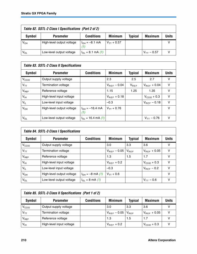
Stratix GX FPGA Family
VOH High-level output voltage IOH = –8.1 mA (1)
VTT + 0.57 V
VOL Low-level output voltage IOL = 8.1 mA (1) VT T – 0.57 V
Table 83. SSTL-2 Class II Specifications
Symbol Parameter Conditions Minimum Typical Maximum Units
VCCIO Output supply voltage 2.3 2.5 2.7 V
VTT Termination voltage VR E F – 0.04 VR E F VR E F + 0.04 V
VREF Reference voltage 1.15 1.25 1.35 V
VIH High-level input voltage VR E F + 0.18 VCCIO + 0.3 V
VIL Low-level input voltage –0.3 VR E F – 0.18 V
VOH High-level output voltage IOH = –16.4 mA (1)
VTT + 0.76 V
VOL Low-level output voltage IOL = 16.4 mA (1) VT T – 0.76 V
Table 84. SSTL-3 Class I Specifications
Symbol Parameter Conditions Minimum Typical Maximum Units
VCCIO Output supply voltage 3.0 3.3 3.6 V
VTT Termination voltage VR E F – 0.05 VR E F VR E F + 0.05 V
VREF Reference voltage 1.3 1.5 1.7 V
VIH High-level input voltage VR E F + 0.2 VCCIO + 0.3 V
VIL Low-level input voltage –0.3 VR E F – 0.2 V
VOH High-level output voltage IOH = –8 mA (1) VTT + 0.6 V
VOL Low-level output voltage IOL = 8 mA (1) VT T – 0.6 V
Table 85. SSTL-3 Class II Specifications (Part 1 of 2)
Symbol Parameter Conditions Minimum Typical Maximum Units
VCCIO Output supply voltage 3.0 3.3 3.6 V
VTT Termination voltage VR E F – 0.05 VR E F VR E F + 0.05 V
VREF Reference voltage 1.3 1.5 1.7 V
VIH High-level input voltage VR E F + 0.2 VCCIO + 0.3 V
Table 82. SSTL-2 Class I Specifications (Part 2 of 2)
Symbol Parameter Conditions Minimum Typical Maximum Units
210 Altera CorporationPreliminary

Operating Conditions
VIL Low-level input voltage –0.3 VR E F – 0.2 V
VOH High-level output voltage IOH = –16 mA (1) VT T + 0.8 V
VOL Low-level output voltage IOL = 16 mA (1) VT T – 0.8 V
Table 86. 3.3-V AGP 2× Specifications
Symbol Parameter Conditions Minimum Typical Maximum Units
VCCIO Output supply voltage 3.15 3.3 3.45 V
VREF Reference voltage 0.39 × VC CI O
0.41 × VC CI O
V
VIH High-level input voltage (2) 0.5 × VC CI O VCCIO + 0.5 V
VIL Low-level input voltage (2) 0.3 × VC CI O V
VOH High-level output voltage IOUT = –0.5 mA 0.9 × VC CI O 3.6 V
VOL Low-level output voltage IOUT = 1.5 mA 0.1 × VC CI O V
Table 87. 3.3-V AGP 1× Specifications
Symbol Parameter Conditions Minimum Typical Maximum Units
VCCIO Output supply voltage 3.15 3.3 3.45 V
VIH High-level input voltage (2) 0.5 × VC CI O VCCIO + 0.5 V
VIL Low-level input voltage (2) 0.3 × VC CI O V
VOH High-level output voltage IOUT = –0.5 mA 0.9 × VC CI O 3.6 V
VOL Low-level output voltage IOUT = 1.5 mA 0.1 × VC CI O V
Table 88. 1.5-V HSTL Class I Specifications (Part 1 of 2)
Symbol Parameter Conditions Minimum Typical Maximum Units
VCCIO Output supply voltage 1.4 1.5 1.6 V
VREF Input reference voltage 0.68 0.75 0.9 V
VTT Termination voltage 0.7 0.75 0.8 V
VIH (DC) DC high-level input voltage VR E F + 0.1 V
VIL (DC) DC low-level input voltage –0.3 VR E F – 0.1 V
VIH (AC) AC high-level input voltage VR E F + 0.2 V
VIL (AC) AC low-level input voltage VR E F – 0.2 V
Table 85. SSTL-3 Class II Specifications (Part 2 of 2)
Symbol Parameter Conditions Minimum Typical Maximum Units
Altera Corporation 211Preliminary

Stratix GX FPGA Family
VOH High-level output voltage IO H = 8 mA (1) VC CI O – 0.4 V
VOL Low-level output voltage IO H = –8 mA (1) 0.4 V
Table 89. 1.5-V HSTL Class II Specifications
Symbol Parameter Conditions Minimum Typical Maximum Units
VCCIO Output supply voltage 1.4 1.5 1.6 V
VREF Input reference voltage 0.68 0.75 0.9 V
VTT Termination voltage 0.7 0.75 0.8 V
VIH (DC) DC high-level input voltage VR E F + 0.1 V
VIL (DC) DC low-level input voltage –0.3 VR E F – 0.1 V
VIH (AC) AC high-level input voltage VR E F + 0.2 V
VIL (AC) AC low-level input voltage VR E F – 0.2 V
VOH High-level output voltage IOH = 16 mA (1) VC CI O – 0.4 V
VOL Low-level output voltage IO H = –16 mA (1) 0.4 V
Table 90. 1.5-V Differential HSTL Specifications
Symbol Parameter Conditions Minimum Typical Maximum Units
VCCIO I/O supply voltage 1.4 1.5 1.6 V
VDIF (DC) DC input differential voltage
0.2 V
VCM (DC) DC common mode input voltage
0.68 0.9 V
VDIF (AC) AC differential input voltage
0.4 V
Table 91. CTT I/O Specifications (Part 1 of 2)
Symbol Parameter Conditions Minimum Typical Maximum Units
VCCIO Output supply voltage 3.0 3.3 3.6 V
VT T/VREF Termination and input reference voltage
1.35 1.5 1.65 V
VIH High-level input voltage VR E F + 0.2 V
VIL Low-level input voltage VR E F – 0.2 V
Table 88. 1.5-V HSTL Class I Specifications (Part 2 of 2)
Symbol Parameter Conditions Minimum Typical Maximum Units
212 Altera CorporationPreliminary
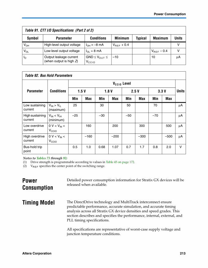
Power Consumption
Power Consumption
Detailed power consumption information for Stratix GX devices will be released when available.
Timing Model The DirectDrive technology and MultiTrack interconnect ensure predictable performance, accurate simulation, and accurate timing analysis across all Stratix GX device densities and speed grades. This section describes and specifies the performance, internal, external, and PLL timing specifications.
All specifications are representative of worst-case supply voltage and junction temperature conditions.
VOH High-level output voltage IOH = –8 mA VR E F + 0.4 V
VOL Low-level output voltage IOL = 8 mA VR E F – 0.4 V
IO Output leakage current (when output is high Z)
GND ≤ VO U T ≤ VC CI O
–10 10 µA
Table 92. Bus Hold Parameters
Parameter Conditions
VC C I O Level
Units1.5 V 1.8 V 2.5 V 3.3 V
Min Max Min Max Min Max Min Max
Low sustaining current
VIN > VIL (maximum)
25 30 50 70 µA
High sustaining current
VIN < VIH (minimum)
–25 –30 –50 –70 µA
Low overdrive current
0 V < VIN < VCCIO
160 200 300 500 µA
High overdrive current
0 V < VIN < VCCIO
–160 –200 –300 –500 µA
Bus-hold trip point
0.5 1.0 0.68 1.07 0.7 1.7 0.8 2.0 V
Notes to Tables 73 through 92:(1) Drive strength is programmable according to values in Table 45 on page 172.(2) VR E F specifies the center point of the switching range.
Table 91. CTT I/O Specifications (Part 2 of 2)
Symbol Parameter Conditions Minimum Typical Maximum Units
Altera Corporation 213Preliminary

Stratix GX FPGA Family
Preliminary & Final Timing
Timing models can have either preliminary or final status. The Quartus II software displays an informational message during the design compilation if the timing models are preliminary. Table 93 shows the status of the Stratix GX device timing models.
Preliminary status means the timing model is subject to change. Initially, timing numbers are created using simulation results, process data, and other known parameters. These tests are used to make the preliminary numbers as close to the actual timing parameters as possible.
Final timing numbers are based on actual device operation and testing. These numbers reflect the actual performance of the device under worst-case voltage and junction temperature conditions.
Performance
Table 94 shows Stratix GX performance for some common designs. All performance values were obtained with Quartus II software compilation of LPM, or MegaCore functions for the FIR and FFT designs.
Table 93. Stratix GX Device Timing Model Status
Device Preliminary Final
EP1SGX10 — v
EP1SGX25 — v
EP1SGX40 — v
Table 94. Stratix Performance (Part 1 of 3) Notes (1), (2)
Applications
Resources Used Performance
LEsTriMatrix Memory Blocks
DSP Blocks
-5 Speed Grade
-6 Speed Grade
-7 Speed Grade
Units
LE 16-to-1 multiplexer (1) 22 0 0 407.83 324.56 288.68 MHz
32-to-1 multiplexer (3) 46 0 0 318.26 255.29 242.89 MHz
16-bit counter 16 0 0 422.11 422.11 390.01 MHz
64-bit counter 64 0 0 321.85 290.52 261.23 MHz
TriMatrix memory M512 block
Simple dual-port RAM 32 × 18 bit
0 1 0 317.76 277.62 241.48 MHz
FIFO 32 × 18 bit 30 1 0 319.18 278.86 242.54 MHz
214 Altera CorporationPreliminary
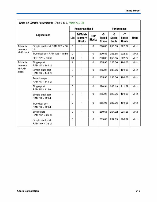
Timing Model
TriMatrix memory M4K block
Simple dual-port RAM 128 × 36 bit
0 1 0 290.86 255.55 222.27 MHz
True dual-port RAM 128 × 18 bit 0 1 0 290.86 255.55 222.27 MHz
FIFO 128 × 36 bit 34 1 0 290.86 255.55 222.27 MHz
TriMatrix memory M-RAM block
Single portRAM 4K × 144 bit
1 1 0 255.95 223.06 194.06 MHz
Simple dual-portRAM 4K × 144 bit
0 1 0 255.95 233.06 194.06 MHz
True dual-portRAM 4K × 144 bit
0 1 0 255.95 233.06 194.06 MHz
Single portRAM 8K × 72 bit
0 1 0 278.94 243.19 211.59 MHz
Simple dual-portRAM 8K × 72 bit
0 1 0 255.95 223.06 194.06 MHz
True dual-portRAM 8K × 72 bit
0 1 0 255.95 223.06 194.06 MHz
Single portRAM 16K × 36 bit
0 1 0 280.66 254.32 221.28 MHz
Simple dual-portRAM 16K × 36 bit
0 1 0 269.83 237.69 206.82 MHz
Table 94. Stratix Performance (Part 2 of 3) Notes (1), (2)
Applications
Resources Used Performance
LEsTriMatrix Memory Blocks
DSP Blocks
-5 Speed Grade
-6 Speed Grade
-7 Speed Grade
Units
Altera Corporation 215Preliminary
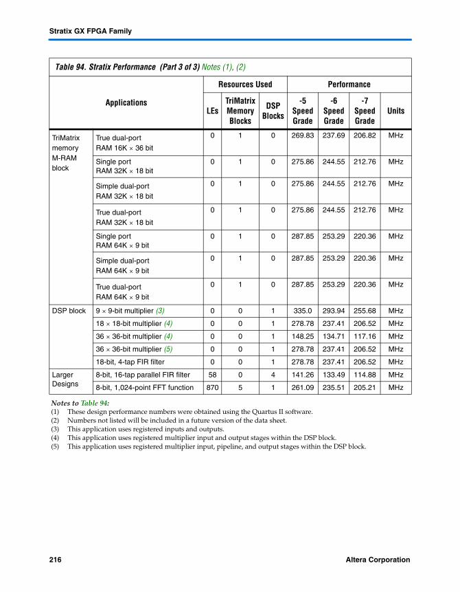
Stratix GX FPGA Family
TriMatrix memory M-RAM block
True dual-portRAM 16K × 36 bit
0 1 0 269.83 237.69 206.82 MHz
Single portRAM 32K × 18 bit
0 1 0 275.86 244.55 212.76 MHz
Simple dual-portRAM 32K × 18 bit
0 1 0 275.86 244.55 212.76 MHz
True dual-portRAM 32K × 18 bit
0 1 0 275.86 244.55 212.76 MHz
Single portRAM 64K × 9 bit
0 1 0 287.85 253.29 220.36 MHz
Simple dual-portRAM 64K × 9 bit
0 1 0 287.85 253.29 220.36 MHz
True dual-portRAM 64K × 9 bit
0 1 0 287.85 253.29 220.36 MHz
DSP block 9 × 9-bit multiplier (3) 0 0 1 335.0 293.94 255.68 MHz
18 × 18-bit multiplier (4) 0 0 1 278.78 237.41 206.52 MHz
36 × 36-bit multiplier (4) 0 0 1 148.25 134.71 117.16 MHz
36 × 36-bit multiplier (5) 0 0 1 278.78 237.41 206.52 MHz
18-bit, 4-tap FIR filter 0 0 1 278.78 237.41 206.52 MHz
Larger Designs
8-bit, 16-tap parallel FIR filter 58 0 4 141.26 133.49 114.88 MHz
8-bit, 1,024-point FFT function 870 5 1 261.09 235.51 205.21 MHz
Notes to Table 94:(1) These design performance numbers were obtained using the Quartus II software.(2) Numbers not listed will be included in a future version of the data sheet.(3) This application uses registered inputs and outputs.(4) This application uses registered multiplier input and output stages within the DSP block.(5) This application uses registered multiplier input, pipeline, and output stages within the DSP block.
Table 94. Stratix Performance (Part 3 of 3) Notes (1), (2)
Applications
Resources Used Performance
LEsTriMatrix Memory Blocks
DSP Blocks
-5 Speed Grade
-6 Speed Grade
-7 Speed Grade
Units
216 Altera CorporationPreliminary
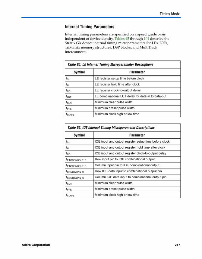
Timing Model
Internal Timing Parameters
Internal timing parameters are specified on a speed grade basis independent of device density. Tables 95 through 101 describe the Stratix GX device internal timing microparameters for LEs, IOEs, TriMatrix memory structures, DSP blocks, and MultiTrack interconnects.
Table 95. LE Internal Timing Microparameter Descriptions
Symbol Parameter
tSU LE register setup time before clock
tH LE register hold time after clock
tCO LE register clock-to-output delay
tLUT LE combinational LUT delay for data-in to data-out
tCLR Minimum clear pulse width
tPRE Minimum preset pulse width
tCLKHL Minimum clock high or low time
Table 96. IOE Internal Timing Microparameter Descriptions
Symbol Parameter
tSU IOE input and output register setup time before clock
tH IOE input and output register hold time after clock
tCO IOE input and output register clock-to-output delay
tPIN2COMBOUT_R Row input pin to IOE combinational output
tPIN2COMBOUT_C Column input pin to IOE combinational output
tCOMBIN2PIN_R Row IOE data input to combinational output pin
tCOMBIN2PIN_C Column IOE data input to combinational output pin
tCLR Minimum clear pulse width
tPRE Minimum preset pulse width
tCLKHL Minimum clock high or low time
Altera Corporation 217Preliminary
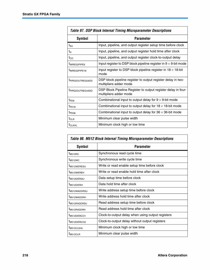
Stratix GX FPGA Family
Table 97. DSP Block Internal Timing Microparameter Descriptions
Symbol Parameter
tSU Input, pipeline, and output register setup time before clock
tH Input, pipeline, and output register hold time after clock
tCO Input, pipeline, and output register clock-to-output delay
tINREG2PIPE9 Input register to DSP block pipeline register in 9 × 9-bit mode
tINREG2PIPE18 Input register to DSP block pipeline register in 18 × 18-bit mode
tPIPE2OUTREG2ADD DSP block pipeline register to output register delay in two-multipliers adder mode
tPIPE2OUTREG4ADD DSP Block Pipeline Register to output register delay in four-multipliers adder mode
tPD9 Combinational input to output delay for 9 × 9-bit mode
tPD18 Combinational input to output delay for 18 × 18-bit mode
tPD36 Combinational input to output delay for 36 × 36-bit mode
tCLR Minimum clear pulse width
tCLKHL Minimum clock high or low time
Table 98. M512 Block Internal Timing Microparameter Descriptions
Symbol Parameter
tM512RC Synchronous read cycle time
tM512WC Synchronous write cycle time
tM512WERESU Write or read enable setup time before clock
tM512WEREH Write or read enable hold time after clock
tM512DATASU Data setup time before clock
tM512DATAH Data hold time after clock
tM512WADDRSU Write address setup time before clock
tM512WADDRH Write address hold time after clock
tM512RADDRSU Read address setup time before clock
tM512RADDRH Read address hold time after clock
tM512DATACO1 Clock-to-output delay when using output registers
tM512DATACO2 Clock-to-output delay without output registers
tM512CLKHL Minimum clock high or low time
tM512CLR Minimum clear pulse width
218 Altera CorporationPreliminary

Timing Model
Table 99. M4K Block Internal Timing Microparameter Descriptions
Symbol Parameter
tM4KRC Synchronous read cycle time
tM4KWC Synchronous write cycle time
tM4KWERESU Write or read enable setup time before clock
tM4KWEREH Write or read enable hold time after clock
tM4KBESU Byte enable setup time before clock
tM4KBEH Byte enable hold time after clock
tM4KDATAASU A port data setup time before clock
tM4KDATAAH A port data hold time after clock
tM4KADDRASU A port address setup time before clock
tM4KADDRAH A port address hold time after clock
tM4KDATABSU B port data setup time before clock
tM4KDATABH B port data hold time after clock
tM4KADDRBSU B port address setup time before clock
tM4KADDRBH B port address hold time after clock
tM4KDATACO1 Clock-to-output delay when using output registers
tM4KDATACO2 Clock-to-output delay without output registers
tM4KCLKHL Minimum clock high or low time
tM4KCLR Minimum clear pulse width
Table 100. M-RAM Block Internal Timing Microparameter Descriptions (Part 1 of 2)
Symbol Parameter
tMRAMRC Synchronous read cycle time
tMRAMWC Synchronous write cycle time
tMRAMWERESU Write or read enable setup time before clock
tMRAMWEREH Write or read enable hold time after clock
tMRAMBESU Byte enable setup time before clock
tMRAMBEH Byte enable hold time after clock
tMRAMDATAASU A port data setup time before clock
tMRAMDATAAH A port data hold time after clock
tMRAMADDRASU A port address setup time before clock
tMRAMADDRAH A port address hold time after clock
Altera Corporation 219Preliminary
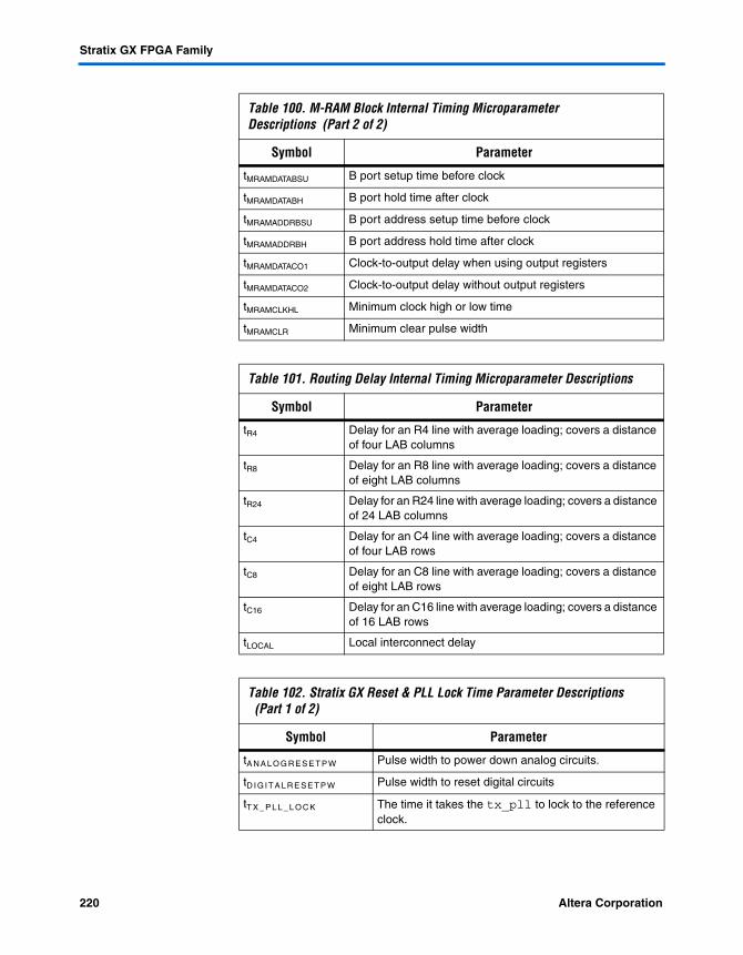
Stratix GX FPGA Family
tMRAMDATABSU B port setup time before clock
tMRAMDATABH B port hold time after clock
tMRAMADDRBSU B port address setup time before clock
tMRAMADDRBH B port address hold time after clock
tMRAMDATACO1 Clock-to-output delay when using output registers
tMRAMDATACO2 Clock-to-output delay without output registers
tMRAMCLKHL Minimum clock high or low time
tMRAMCLR Minimum clear pulse width
Table 101. Routing Delay Internal Timing Microparameter Descriptions
Symbol Parameter
tR4 Delay for an R4 line with average loading; covers a distance of four LAB columns
tR8 Delay for an R8 line with average loading; covers a distance of eight LAB columns
tR24 Delay for an R24 line with average loading; covers a distance of 24 LAB columns
tC4 Delay for an C4 line with average loading; covers a distance of four LAB rows
tC8 Delay for an C8 line with average loading; covers a distance of eight LAB rows
tC16 Delay for an C16 line with average loading; covers a distance of 16 LAB rows
tLOCAL Local interconnect delay
Table 102. Stratix GX Reset & PLL Lock Time Parameter Descriptions(Part 1 of 2)
Symbol Parameter
tA NA L O G R E S E T P W Pulse width to power down analog circuits.
tD I G I T A L R E S E T P W Pulse width to reset digital circuits
tT X _ P L L _ L O C K The time it takes the tx_pll to lock to the reference clock.
Table 100. M-RAM Block Internal Timing Microparameter Descriptions (Part 2 of 2)
Symbol Parameter
220 Altera CorporationPreliminary
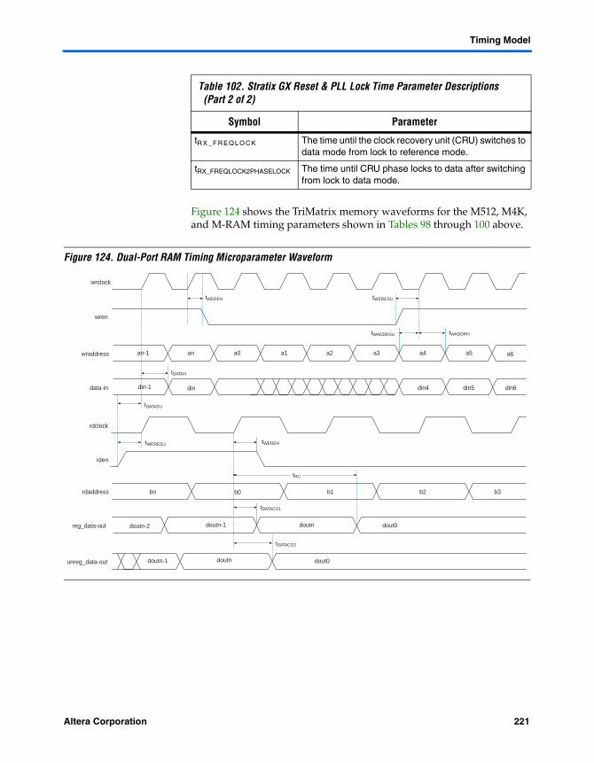
Timing Model
Figure 124 shows the TriMatrix memory waveforms for the M512, M4K, and M-RAM timing parameters shown in Tables 98 through 100 above.
Figure 124. Dual-Port RAM Timing Microparameter Waveform
tR X _ F R E Q L O C K The time until the clock recovery unit (CRU) switches to data mode from lock to reference mode.
tRX_FREQLOCK2PHASELOCK The time until CRU phase locks to data after switching from lock to data mode.
Table 102. Stratix GX Reset & PLL Lock Time Parameter Descriptions(Part 2 of 2)
Symbol Parameter
wrclock
wren
wraddress
data-in
reg_data-out
an-1 an a0 a1 a2 a3 a4 a5
din-1 din din4 din5
rdclock
a6
din6
unreg_data-out
rden
rdaddress bn b0 b1 b2 b3
doutn-2 doutn-1 doutn
doutn-1 doutn dout0
tWERESU tWEREH
tDATACO1
tDATACO2
tDATASU
tDATAH
tWEREH tWERESU
tWADDRSU tWADDRH
dout0
tRC
Altera Corporation 221Preliminary
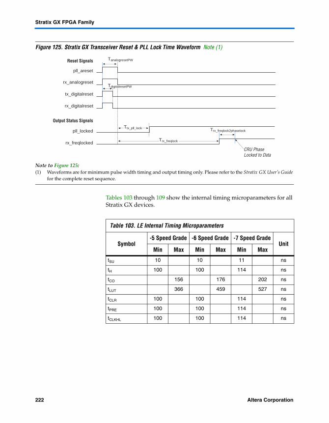
Stratix GX FPGA Family
Figure 125. Stratix GX Transceiver Reset & PLL Lock Time Waveform Note (1)
Note to Figure 125:(1) Waveforms are for minimum pulse width timing and output timing only. Please refer to the Stratix GX User’s Guide
for the complete reset sequence.
Tables 103 through 109 show the internal timing microparameters for all Stratix GX devices.
rx_analogreset
tx_digitalreset
rx_digitalreset
pll_locked
rx_freqlocked
pll_areset
Reset Signals
Output Status Signals
TanalogresetPW
TdigitalresetPW
Ttx_pll_lock Trx_freqlock2phaselock
Trx_freqlock
CRU PhaseLocked to Data
Table 103. LE Internal Timing Microparameters
Symbol-5 Speed Grade -6 Speed Grade -7 Speed Grade
UnitMin Max Min Max Min Max
tSU 10 10 11 ns
tH 100 100 114 ns
tCO 156 176 202 ns
tLUT 366 459 527 ns
tCLR 100 100 114 ns
tPRE 100 100 114 ns
tCLKHL 100 100 114 ns
222 Altera CorporationPreliminary

Timing Model
Table 104. IOE Internal Timing Microparameters
Symbol-5 Speed Grade -6 Speed Grade -7 Speed Grade
UnitMin Max Min Max Min Max
tSU 64 68 68 ns
tH 76 80 80 ns
tCO 162 171 171 ns
tPIN2COMBOUT_R 1,038 1,093 1,256 ns
tPIN2COMBOUT_C 927 976 1,122 ns
tCOMBIN2PIN_R 2,944 3,099 3,563 ns
tCOMBIN2PIN_C 3,189 3,357 3,860 ns
tCLR 262 276 317 ns
tPRE 262 276 317 ns
tCLKHL 90 95 109 ns
Table 105. DSP Block Internal Timing Microparameters
Symbol
-5 Speed Grade
-6 Speed Grade
-7 Speed Grade Unit
Min Max Min Max Min Max
tSU 0 0 0 ns
tH 67 75 86 ns
tCO 142 158 181 ns
tINREG2PIPE18 2,613 2,982 3,429 ns
tINREG2PIPE9 3,390 3,993 4,591 ns
tPIPE2OUTREG2ADD 2,002 2,203 2,533 ns
tPIPE2OUTREG4ADD 2,899 3,189 3,667 ns
tPD9 3,709 4,081 4,692 ns
tPD18 4,795 5,275 6,065 ns
tPD36 7,495 8,245 9,481 ns
tCLR 450 500 575 ns
tCLKHL 1,350 1,500 1,724 ns
Altera Corporation 223Preliminary

Stratix GX FPGA Family
Table 106. M512 Block Internal Timing Microparameters
Symbol-5 Speed Grade -6 Speed Grade -7 Speed Grade
UnitMin Max Min Max Min Max
tM512RC 3,340 3,816 4,387 ns
tM512WC 3,318 3,590 4,128 ns
tM512WERESU 110 123 141 ns
tM512WERH 34 38 43 ns
tM512DATASU 110 123 141 ns
tM512DATAH 34 38 43 ns
tM512WADDRASU 110 123 141 ns
tM512WADDRH 34 38 43 ns
tM512DATACO1 424 472 541 ns
tM512DATACO2 3,366 3,846 4,421 ns
tM512CLKHL 150 167 192 ns
tM512CLR 170 189 217 ns
Table 107. M4K Block Internal Timing Microparameters (Part 1 of 2)
Symbol-5 Speed Grade -6 Speed Grade -7 Speed Grade
UnitMin Max Min Max Min Max
tM4KRC 3,807 4,320 4,967 ns
tM4KWC 2,556 2,840 3,265 ns
tM4KWERESU 131 149 171 ns
tM4KWERH 34 38 43 ns
tM4KDATASU 131 149 171 ns
tM4KDATAH 34 38 43 ns
tM4KWADDRASU 131 149 171 ns
tM4KWADDRH 34 38 43 ns
tM4KRADDRASU 131 149 171 ns
tM4KRADDRH 34 38 43 ns
tM4KDATABSU 131 149 171 ns
tM4KDATABH 34 38 43 ns
tM4KADDRBSU 131 149 171 ns
tM4KADDRBH 34 38 43 ns
224 Altera CorporationPreliminary

Timing Model
tM4KDATACO1 571 635 729 ns
tM4KDATACO2 3,984 4,507 5,182 ns
tM4KCLKHL 150 167 192 ns
tM4KCLR 170 189 255 ns
Table 108. M-RAM Block Internal Timing Microparameters
Symbol-5 -6 -7
UnitMin Max Min Max Min Max
tMRAMRC 4,364 4,838 5,562 ns
tMRAMWC 3,654 4,127 4,746 ns
tMRAMWERESU 25 25 28 ns
tMRAMWERH 18 20 23 ns
tMRAMDATASU 25 25 28 ns
tMRAMDATAH 18 20 23 ns
tMRAMWADDRASU 25 25 28 ns
tMRAMWADDRH 18 20 23 ns
tMRAMRADDRASU 25 25 28 ns
tMRAMRADDRH 18 20 23 ns
tMRAMDATABSU 25 25 28 ns
tMRAMDATABH 18 20 23 ns
tMRAMADDRBSU 25 25 28 ns
tMRAMADDRBH 18 20 23 ns
tMRAMDATACO1 1,038 1,053 1,210 ns
tMRAMDATACO2 4,362 4,939 5,678 ns
tMRAMCLKHL 270 300 345 ns
tMRAMCLR 135 150 172 ns
Table 107. M4K Block Internal Timing Microparameters (Part 2 of 2)
Symbol-5 Speed Grade -6 Speed Grade -7 Speed Grade
UnitMin Max Min Max Min Max
Altera Corporation 225Preliminary

Stratix GX FPGA Family
Routing delays vary depending on the load on a specific routing line. The Quartus II software reports the routing delay information when running the timing analysis for a design. Contact Altera Applications Engineering for more details.
External Timing Parameters
External timing parameters are specified by device density and speed grade. Figure 126 shows the timing model for bidirectional IOE pin timing. All registers are within the IOE.
Table 109. Stratix GX Transceiver Reset & PLL Lock Time Parameters
Symbol Min Typ Max Units
tA N A L O G R E S E T P W (5) 1 mS
tD I G I TA L R E S E T P W (5) 4 Parallel clock cycle
tT X _ P L L _ L O C K (3) 10 µS
tR X _ F R E Q L O C K (4) 5 mS
tR X _ F R E Q L O C K 2 P H A S E L O C K (2) 2 mS
Notes to Table 109:(1) The minimum pulse width specified is associated with the power-down of circuits.(2) The clock recovery unit (CRU) phase locked-to-data time is based on a data rate of 500 Mbps and 8B/10B encoded
data.(3) After #pll_areset, pll_enable, or PLL power-up, the time required for the transceiver PLL to lock to the
reference clock.(4) After #rx_analogreset, the time for the CRU to switch to lock-to-data mode.(5) There is no maximum pulse width specification. The GXB can be held in reset indefinitely.
226 Altera CorporationPreliminary
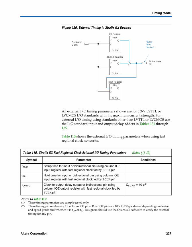
Timing Model
Figure 126. External Timing in Stratix GX Devices
All external I/O timing parameters shown are for 3.3-V LVTTL or LVCMOS I/O standards with the maximum current strength. For external I/O timing using standards other than LVTTL or LVCMOS use the I/O standard input and output delay adders in Tables 131 through 135.
Table 110 shows the external I/O timing parameters when using fast regional clock networks.
PRN
CLRN
D Q
PRN
CLRN
D Q
PRN
CLRN
D Q
DedicatedClock
BidirectionalPin
Output Register
Input Register
OE Register
tINSUtINHtOUTCO
Table 110. Stratix GX Fast Regional Clock External I/O Timing Parameters Notes (1), (2)
Symbol Parameter Conditions
tINSU Setup time for input or bidirectional pin using column IOE input register with fast regional clock fed by FCLK pin
tINH Hold time for input or bidirectional pin using column IOE input register with fast regional clock fed by FCLK pin
tOUTCO Clock-to-output delay output or bidirectional pin using column IOE output register with fast regional clock fed by FCLK pin
CL OA D = 10 pF
Notes to Table 110:(1) These timing parameters are sample-tested only.(2) These timing parameters are for column IOE pins. Row IOE pins are 100- to 250-ps slower depending on device
and speed grade and whether it is tCO or tSU. Designers should use the Quartus II software to verify the external timing for any pin.
Altera Corporation 227Preliminary
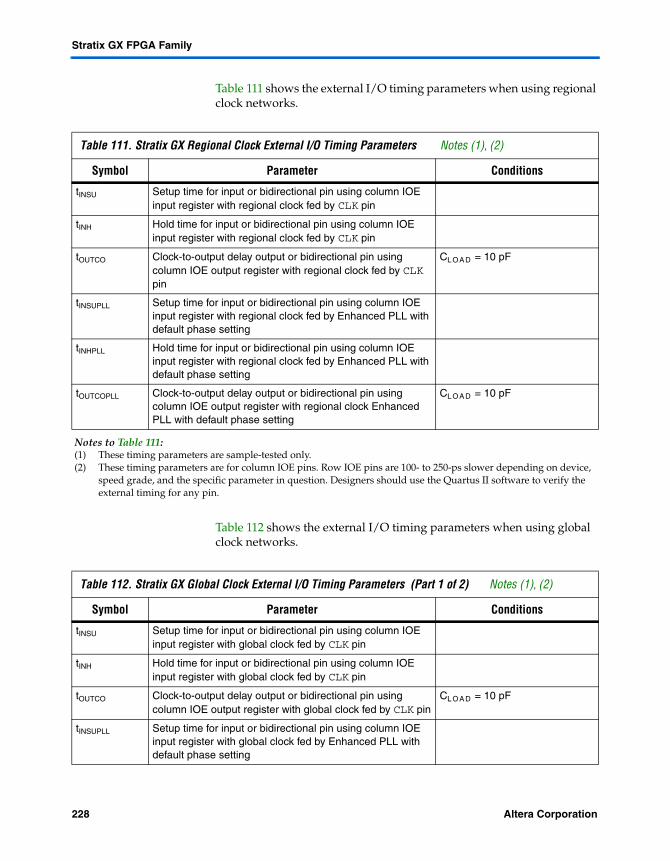
Stratix GX FPGA Family
Table 111 shows the external I/O timing parameters when using regional clock networks.
Table 112 shows the external I/O timing parameters when using global clock networks.
Table 111. Stratix GX Regional Clock External I/O Timing Parameters Notes (1), (2)
Symbol Parameter Conditions
tINSU Setup time for input or bidirectional pin using column IOE input register with regional clock fed by CLK pin
tINH Hold time for input or bidirectional pin using column IOE input register with regional clock fed by CLK pin
tOUTCO Clock-to-output delay output or bidirectional pin using column IOE output register with regional clock fed by CLK pin
CL OA D = 10 pF
tINSUPLL Setup time for input or bidirectional pin using column IOE input register with regional clock fed by Enhanced PLL with default phase setting
tINHPLL Hold time for input or bidirectional pin using column IOE input register with regional clock fed by Enhanced PLL with default phase setting
tOUTCOPLL Clock-to-output delay output or bidirectional pin using column IOE output register with regional clock Enhanced PLL with default phase setting
CL OA D = 10 pF
Notes to Table 111:(1) These timing parameters are sample-tested only.(2) These timing parameters are for column IOE pins. Row IOE pins are 100- to 250-ps slower depending on device,
speed grade, and the specific parameter in question. Designers should use the Quartus II software to verify the external timing for any pin.
Table 112. Stratix GX Global Clock External I/O Timing Parameters (Part 1 of 2) Notes (1), (2)
Symbol Parameter Conditions
tINSU Setup time for input or bidirectional pin using column IOE input register with global clock fed by CLK pin
tINH Hold time for input or bidirectional pin using column IOE input register with global clock fed by CLK pin
tOUTCO Clock-to-output delay output or bidirectional pin using column IOE output register with global clock fed by CLK pin
CL OA D = 10 pF
tINSUPLL Setup time for input or bidirectional pin using column IOE input register with global clock fed by Enhanced PLL with default phase setting
228 Altera CorporationPreliminary
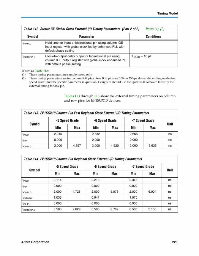
Timing Model
Tables 113 through 118 show the external timing parameters on column and row pins for EP1SGX10 devices.
tINHPLL Hold time for input or bidirectional pin using column IOE input register with global clock fed by enhanced PLL with default phase setting
tOUTCOPLL Clock-to-output delay output or bidirectional pin using column IOE output register with global clock enhanced PLL with default phase setting
CL OA D = 10 pF
Notes to Table 112:(1) These timing parameters are sample-tested only.(2) These timing parameters are for column IOE pins. Row IOE pins are 100- to 250-ps slower depending on device,
speed grade, and the specific parameter in question. Designers should use the Quartus II software to verify the external timing for any pin.
Table 112. Stratix GX Global Clock External I/O Timing Parameters (Part 2 of 2) Notes (1), (2)
Symbol Parameter Conditions
Table 113. EP1SGX10 Column Pin Fast Regional Clock External I/O Timing Parameters
Symbol-5 Speed Grade -6 Speed Grade -7 Speed Grade
UnitMin Max Min Max Min Max
tINSU 2.245 2.332 2.666 ns
tINH 0.000 0.000 0.000 ns
tOUTCO 2.000 4.597 2.000 4.920 2.000 5.635 ns
Table 114. EP1SGX10 Column Pin Regional Clock External I/O Timing Parameters
Symbol-5 Speed Grade -6 Speed Grade -7 Speed Grade
UnitMin Max Min Max Min Max
tINSU 2.114 2.218 2.348 ns
tINH 0.000 0.000 0.000 ns
tOUTCO 2.000 4.728 2.000 5.078 2.000 6.004 ns
tINSUPLL 1.035 0.941 1.070 ns
tINHPLL 0.000 0.000 0.000 ns
tOUTCOPLL 0.500 2.629 0.500 2.769 0.500 3.158 ns
Altera Corporation 229Preliminary

Stratix GX FPGA Family
Table 115. EP1SGX10 Column Pin Global Clock External I/O Timing Parameters
Symbol-5 Speed Grade -6 Speed Grade -7 Speed Grade
UnitMin Max Min Max Min Max
tINSU 1.785 1.814 2.087 ns
tINH 0.000 0.000 0.000 ns
tOUTCO 2.000 5.057 2.000 5.438 2.000 6.214 ns
tINSUPLL 0.988 0.936 1.066 ns
tINHPLL 0.000 0.000 0.000 ns
tOUTCOPLL 0.500 2.634 0.500 2.774 0.500 3.162 ns
Table 116. EP1SGX10 Row Pin Fast Regional Clock External I/O Timing Parameters
Symbol-5 Speed Grade -6 Speed Grade -7 Speed Grade
UnitMin Max Min Max Min Max
tINSU 2.194 2.384 2.727 ns
tINH 0.000 0.000 0.000 ns
tOUTCO 2.000 4.956 2.000 4.971 2.000 5.463 ns
Table 117. EP1SGX10 Row Pin Regional Clock External I/O Timing Parameters
Symbol-5 Speed Grade -6 Speed Grade -7 Speed Grade
UnitMin Max Min Max Min Max
tINSU 2.244 2.413 2.574 ns
tINH 0.000 0.000 0.000 ns
tOUTCO 2.000 4.906 2.000 4.942 2.000 5.616 ns
tINSUPLL 1.126 1.186 1.352 ns
tINHPLL 0.000 0.000 0.000 ns
tOUTCOPLL 0.500 2.804 0.500 2.627 0.500 2.765 ns
Table 118. EP1SGX10 Row Pin Global Clock External I/O Timing Parameters (Part 1 of 2)
Symbol-5 Speed Grade -6 Speed Grade -7 Speed Grade
UnitMin Max Min Max Min Max
tINSU 1.919 2.062 2.368 ns
tINH 0.000 0.000 0.000 ns
230 Altera CorporationPreliminary
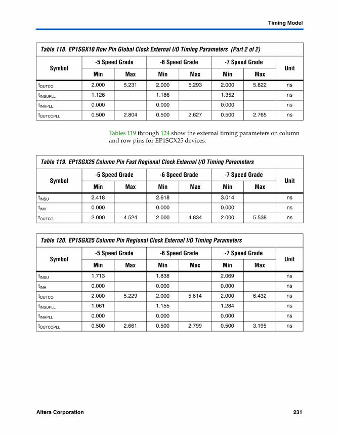
Timing Model
Tables 119 through 124 show the external timing parameters on column and row pins for EP1SGX25 devices.
tOUTCO 2.000 5.231 2.000 5.293 2.000 5.822 ns
tINSUPLL 1.126 1.186 1.352 ns
tINHPLL 0.000 0.000 0.000 ns
tOUTCOPLL 0.500 2.804 0.500 2.627 0.500 2.765 ns
Table 118. EP1SGX10 Row Pin Global Clock External I/O Timing Parameters (Part 2 of 2)
Symbol-5 Speed Grade -6 Speed Grade -7 Speed Grade
UnitMin Max Min Max Min Max
Table 119. EP1SGX25 Column Pin Fast Regional Clock External I/O Timing Parameters
Symbol-5 Speed Grade -6 Speed Grade -7 Speed Grade
UnitMin Max Min Max Min Max
tINSU 2.418 2.618 3.014 ns
tINH 0.000 0.000 0.000 ns
tOUTCO 2.000 4.524 2.000 4.834 2.000 5.538 ns
Table 120. EP1SGX25 Column Pin Regional Clock External I/O Timing Parameters
Symbol-5 Speed Grade -6 Speed Grade -7 Speed Grade
UnitMin Max Min Max Min Max
tINSU 1.713 1.838 2.069 ns
tINH 0.000 0.000 0.000 ns
tOUTCO 2.000 5.229 2.000 5.614 2.000 6.432 ns
tINSUPLL 1.061 1.155 1.284 ns
tINHPLL 0.000 0.000 0.000 ns
tOUTCOPLL 0.500 2.661 0.500 2.799 0.500 3.195 ns
Altera Corporation 231Preliminary

Stratix GX FPGA Family
Table 121. EP1SGX25 Column Pin Global Clock External I/O Timing Parameters
Symbol-5 Speed Grade -6 Speed Grade -7 Speed Grade
UnitMin Max Min Max Min Max
tINSU 1.790 1.883 2.120 ns
tINH 0.000 0.000 0.000 ns
tOUTCO 2.000 5.194 2.000 5.569 2.000 6.381 ns
tINSUPLL 1.046 1.141 1.220 ns
tINHPLL 0.000 0.000 0.000 ns
tOUTCOPLL 0.500 2.676 0.500 2.813 0.500 3.208 ns
Table 122. EP1SGX25 Row Pin Fast Regional Clock External I/O Timing Parameters
Symbol-5 Speed Grade -6 Speed Grade -7 Speed Grade
UnitMin Max Min Max Min Max
tINSU 2.394 2.594 2.936 ns
tINH 0.000 0.000 0.000 ns
tOUTCO 2.000 4.456 2.000 4.761 2.000 5.454 ns
Table 123. EP1SGX25 Row Pin Regional Clock External I/O Timing Parameters
Symbol-5 Speed Grade -6 Speed Grade -7 Speed Grade
UnitMin Max Min Max Min Max
tINSU 1.970 2.109 2.377 ns
tINH 0.000 0.000 0.000 ns
tOUTCO 2.000 4.880 2.000 5.246 2.000 6.013 ns
tINSUPLL 1.326 1.386 1.552 ns
tINHPLL 0.000 0.000 0.000 ns
tOUTCOPLL 0.500 2.304 0.500 2.427 0.500 2.765 ns
Table 124. EP1SGX25 Row Pin Global Clock External I/O Timing Parameters (Part 1 of 2)
Symbol-5 Speed Grade -6 Speed Grade -7 Speed Grade
UnitMin Max Min Max Min Max
tINSU 1.963 2.108 2.379 ns
tINH 0.000 0.000 0.000 ns
232 Altera CorporationPreliminary
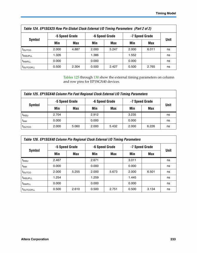
Timing Model
Tables 125 through 130 show the external timing parameters on column and row pins for EP1SGX40 devices.
tOUTCO 2.000 4.887 2.000 5.247 2.000 6.011 ns
tINSUPLL 1.326 1.386 1.552 ns
tINHPLL 0.000 0.000 0.000 ns
tOUTCOPLL 0.500 2.304 0.500 2.427 0.500 2.765 ns
Table 124. EP1SGX25 Row Pin Global Clock External I/O Timing Parameters (Part 2 of 2)
Symbol-5 Speed Grade -6 Speed Grade -7 Speed Grade
UnitMin Max Min Max Min Max
Table 125. EP1SGX40 Column Pin Fast Regional Clock External I/O Timing Parameters
Symbol-5 Speed Grade -6 Speed Grade -7 Speed Grade
UnitMin Max Min Max Min Max
tINSU 2.704 2.912 3.235 ns
tINH 0.000 0.000 0.000 ns
tOUTCO 2.000 5.060 2.000 5.432 2.000 6.226 ns
Table 126. EP1SGX40 Column Pin Regional Clock External I/O Timing Parameters
Symbol-5 Speed Grade -6 Speed Grade -7 Speed Grade
UnitMin Max Min Max Min Max
tINSU 2.467 2.671 3.011 ns
tINH 0.000 0.000 0.000 ns
tOUTCO 2.000 5.255 2.000 5.673 2.000 6.501 ns
tINSUPLL 1.254 1.259 1.445 ns
tINHPLL 0.000 0.000 0.000 ns
tOUTCOPLL 0.500 2.610 0.500 2.751 0.500 3.134 ns
Altera Corporation 233Preliminary

Stratix GX FPGA Family
Table 127. EP1SGX40 Column Pin Global Clock External I/O Timing Parameters
Symbol-5 Speed Grade -6 Speed Grade -7 Speed Grade
UnitMin Max Min Max Min Max
tINSU 2.033 2.184 2.451 ns
tINH 0.000 0.000 0.000 ns
tOUTCO 2.000 5.689 2.000 6.116 2.000 7.010 ns
tINSUPLL 1.228 1.278 1.415 ns
tINHPLL 0.000 0.000 0.000 ns
tOUTCOPLL 0.500 2.594 0.500 2.732 0.500 3.113 ns
Table 128. EP1SGX40 Row Pin Fast Regional Clock External I/O Timing Parameters
Symbol-5 Speed Grade -6 Speed Grade -7 Speed Grade
UnitMin Max Min Max Min Max
tINSU 2.450 2.662 3.046 ns
tINH 0.000 0.000 0.000 ns
tOUTCO 2.000 4.880 2.000 5.241 2.000 6.004 ns
Table 129. EP1SGX40 Row Pin Regional Clock External I/O Timing Parameters
Symbol-5 Speed Grade -6 Speed Grade -7 Speed Grade
UnitMin Max Min Max Min Max
tINSU 2.398 2.567 2.938 ns
tINH 0.000 0.000 0.000 ns
tOUTCO 2.000 4.932 2.000 5.336 2.000 6.112 ns
tINSUPLL 1.126 1.186 1.352 ns
tINHPLL 0.000 0.000 0.000 ns
tOUTCOPLL 0.500 2.304 0.500 2.427 0.500 2.765 ns
Table 130. EP1SGX40 Row Pin Global Clock External I/O Timing Parameters (Part 1 of 2)
Symbol-5 Speed Grade -6 Speed Grade -7 Speed Grade
UnitMin Max Min Max Min Max
tINSU 1.965 2.128 2.429 ns
tINH 0.000 0.000 0.000 ns
234 Altera CorporationPreliminary

Timing Model
External I/O Delay Parameters
External I/O delay timing parameters, both for I/O standard input and output adders and programmable input and output delays, are specified by speed grade, independent of device density.
Tables 131 through 136 show the adder delays associated with column and row I/O pins. If an I/O standard is selected other than LVTTL 24 mA with a fast slew rate, add the selected delay to the external tCO and tSU I/O parameters.
tOUTCO 2.000 5.365 2.000 5.775 2.000 6.621 ns
tINSUPLL 1.126 1.186 1.352 ns
tINHPLL 0.000 0.000 0.000 ns
tOUTCOPLL 0.500 2.304 0.500 2.427 0.500 2.765 ns
Table 130. EP1SGX40 Row Pin Global Clock External I/O Timing Parameters (Part 2 of 2)
Symbol-5 Speed Grade -6 Speed Grade -7 Speed Grade
UnitMin Max Min Max Min Max
Table 131. Stratix GX I/O Standard Column Pin Input Delay Adders (Part 1 of 2)
I/O Standard-5 Speed Grade -6 Speed Grade -7 Speed Grade
UnitMin Max Min Max Min Max
LVCMOS 0 0 0 ps
3.3-V LVTTL 0 0 0 ps
2.5-V LVTTL 30 31 35 ps
1.8-V LVTTL 150 157 180 ps
1.5-V LVTTL 210 220 252 ps
GTL 220 231 265 ps
GTL+ 220 231 265 ps
3.3-V PCI 0 0 0 ps
3.3-V PCI-X 1.0 0 0 0 ps
Compact PCI 0 0 0 ps
AGP 1× 0 0 0 ps
AGP 2× 0 0 0 ps
CTT 120 126 144 ps
SSTL-3 class I –30 –32 –37 ps
SSTL-3 class II –30 –32 –37 ps
Altera Corporation 235Preliminary
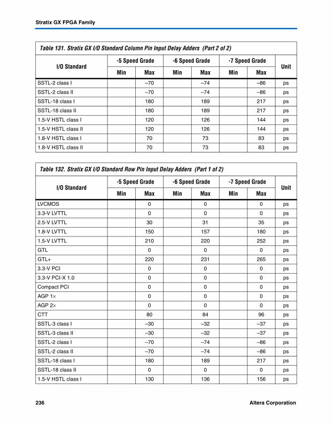
Stratix GX FPGA Family
SSTL-2 class I –70 –74 –86 ps
SSTL-2 class II –70 –74 –86 ps
SSTL-18 class I 180 189 217 ps
SSTL-18 class II 180 189 217 ps
1.5-V HSTL class I 120 126 144 ps
1.5-V HSTL class II 120 126 144 ps
1.8-V HSTL class I 70 73 83 ps
1.8-V HSTL class II 70 73 83 ps
Table 132. Stratix GX I/O Standard Row Pin Input Delay Adders (Part 1 of 2)
I/O Standard-5 Speed Grade -6 Speed Grade -7 Speed Grade
UnitMin Max Min Max Min Max
LVCMOS 0 0 0 ps
3.3-V LVTTL 0 0 0 ps
2.5-V LVTTL 30 31 35 ps
1.8-V LVTTL 150 157 180 ps
1.5-V LVTTL 210 220 252 ps
GTL 0 0 0 ps
GTL+ 220 231 265 ps
3.3-V PCI 0 0 0 ps
3.3-V PCI-X 1.0 0 0 0 ps
Compact PCI 0 0 0 ps
AGP 1× 0 0 0 ps
AGP 2× 0 0 0 ps
CTT 80 84 96 ps
SSTL-3 class I –30 –32 –37 ps
SSTL-3 class II –30 –32 –37 ps
SSTL-2 class I –70 –74 –86 ps
SSTL-2 class II –70 –74 –86 ps
SSTL-18 class I 180 189 217 ps
SSTL-18 class II 0 0 0 ps
1.5-V HSTL class I 130 136 156 ps
Table 131. Stratix GX I/O Standard Column Pin Input Delay Adders (Part 2 of 2)
I/O Standard-5 Speed Grade -6 Speed Grade -7 Speed Grade
UnitMin Max Min Max Min Max
236 Altera CorporationPreliminary
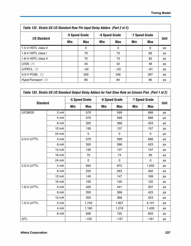
Timing Model
1.5-V HSTL class II 0 0 0 ps
1.8-V HSTL class I 70 73 83 ps
1.8-V HSTL class II 70 73 83 ps
LVDS (1) 40 42 48 ps
LVPECL (1) –50 –53 –61 ps
3.3-V PCML (1) 330 346 397 ps
HyperTransport (1) 80 84 96 ps
Table 133. Stratix GX I/O Standard Output Delay Adders for Fast Slew Rate on Column Pins (Part 1 of 2)
Standard-5 Speed Grade -6 Speed Grade -7 Speed Grade
UnitMin Max Min Max Min Max
LVCMOS 2 mA 570 599 689 ps
4 mA 570 599 689 ps
8 mA 350 368 423 ps
12 mA 130 137 157 ps
24 mA 0 0 0 ps
3.3-V LVTTL 4 mA 570 599 689 ps
8 mA 350 368 423 ps
12 mA 130 137 157 ps
16 mA 70 74 85 ps
24 mA 0 0 0 ps
2.5-V LVTTL 2 mA 830 872 1,002 ps
8 mA 250 263 302 ps
12 mA 140 147 169 ps
16 mA 100 105 120 ps
1.8-V LVTTL 2 mA 420 441 507 ps
8 mA 350 368 423 ps
12 mA 350 368 423 ps
1.5-V LVTTL 2 mA 1,740 1,827 2,101 ps
4 mA 1,160 1,218 1,400 ps
8 mA 690 725 833 ps
GTL –150 –157 –181 ps
Table 132. Stratix GX I/O Standard Row Pin Input Delay Adders (Part 2 of 2)
I/O Standard-5 Speed Grade -6 Speed Grade -7 Speed Grade
UnitMin Max Min Max Min Max
Altera Corporation 237Preliminary

Stratix GX FPGA Family
GTL+ –110 –115 –133 ps
3.3-V PCI –230 –241 –277 ps
3.3-V PCI-X 1.0 –230 –241 –277 ps
Compact PCI –230 –241 –277 ps
AGP 1× –30 –31 –36 ps
AGP 2× –30 –31 –36 ps
CTT 50 53 61 ps
SSTL-3 class I 90 95 109 ps
SSTL-3 class II –50 –52 –60 ps
SSTL-2 class I 100 105 120 ps
SSTL-2 class II 20 21 24 ps
SSTL-18 class I 230 242 278 ps
SSTL-18 class II 0 0 0 ps
1.5-V HSTL class I 380 399 459 ps
1.5-V HSTL class II 190 200 230 ps
1.8-V HSTL class I 380 399 459 ps
1.8-V HSTL class II 390 410 471 ps
Table 134. Stratix GX I/O Standard Output Delay Adders for Fast Slew Rate on Row Pins (Part 1 of 2)
Standard-5 Speed Grade -6 Speed Grade -7 Speed Grade
UnitMin Max Min Max Min Max
LVCMOS 2 mA 570 599 689 ps
4 mA 570 599 689 ps
8 mA 350 368 423 ps
12 mA 130 137 157 ps
24 mA 0 0 0 ps
3.3-V LVTTL 4 mA 570 599 689 ps
8 mA 350 368 423 ps
12 mA 130 137 157 ps
16 mA 70 74 85 ps
24 mA 0 0 0 ps
Table 133. Stratix GX I/O Standard Output Delay Adders for Fast Slew Rate on Column Pins (Part 2 of 2)
Standard-5 Speed Grade -6 Speed Grade -7 Speed Grade
UnitMin Max Min Max Min Max
238 Altera CorporationPreliminary
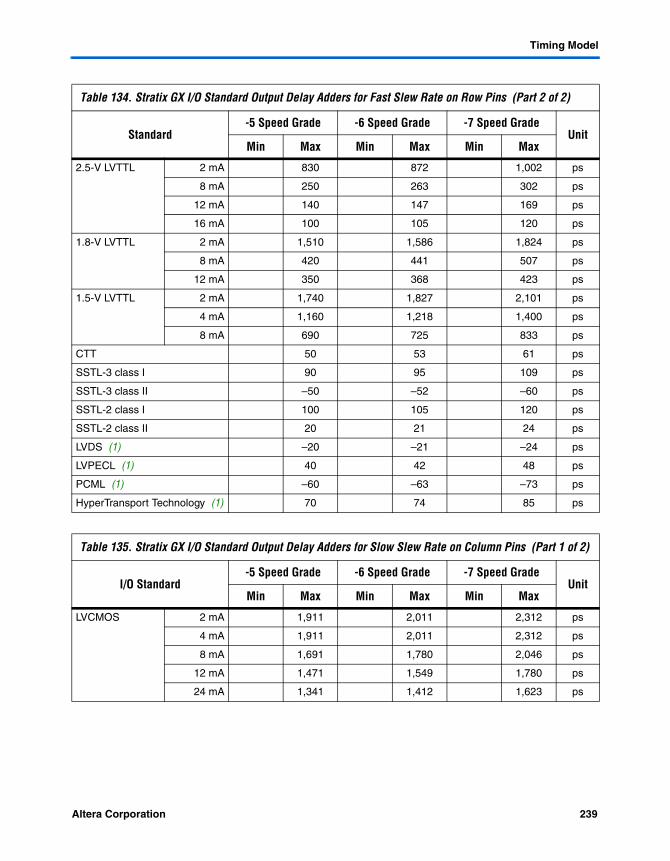
Timing Model
2.5-V LVTTL 2 mA 830 872 1,002 ps
8 mA 250 263 302 ps
12 mA 140 147 169 ps
16 mA 100 105 120 ps
1.8-V LVTTL 2 mA 1,510 1,586 1,824 ps
8 mA 420 441 507 ps
12 mA 350 368 423 ps
1.5-V LVTTL 2 mA 1,740 1,827 2,101 ps
4 mA 1,160 1,218 1,400 ps
8 mA 690 725 833 ps
CTT 50 53 61 ps
SSTL-3 class I 90 95 109 ps
SSTL-3 class II –50 –52 –60 ps
SSTL-2 class I 100 105 120 ps
SSTL-2 class II 20 21 24 ps
LVDS (1) –20 –21 –24 ps
LVPECL (1) 40 42 48 ps
PCML (1) –60 –63 –73 ps
HyperTransport Technology (1) 70 74 85 ps
Table 135. Stratix GX I/O Standard Output Delay Adders for Slow Slew Rate on Column Pins (Part 1 of 2)
I/O Standard-5 Speed Grade -6 Speed Grade -7 Speed Grade
UnitMin Max Min Max Min Max
LVCMOS 2 mA 1,911 2,011 2,312 ps
4 mA 1,911 2,011 2,312 ps
8 mA 1,691 1,780 2,046 ps
12 mA 1,471 1,549 1,780 ps
24 mA 1,341 1,412 1,623 ps
Table 134. Stratix GX I/O Standard Output Delay Adders for Fast Slew Rate on Row Pins (Part 2 of 2)
Standard-5 Speed Grade -6 Speed Grade -7 Speed Grade
UnitMin Max Min Max Min Max
Altera Corporation 239Preliminary

Stratix GX FPGA Family
3.3-V LVTTL 4 mA 1,993 2,097 2,411 ps
8 mA 1,773 1,866 2,145 ps
12 mA 1,553 1,635 1,879 ps
16 mA 1,493 1,572 1,807 ps
24 mA 1,423 1,498 1,722 ps
2.5-V LVTTL 2 mA 2,631 2,768 3,182 ps
8 mA 2,051 2,159 2,482 ps
12 mA 1,941 2,043 2,349 ps
16 mA 1,901 2,001 2,300 ps
1.8-V LVTTL 2 mA 4,632 4,873 5,604 ps
8 mA 3,542 3,728 4,287 ps
12 mA 3,472 3,655 4,203 ps
1.5-V LVTTL 2 mA 6,620 6,964 8,008 ps
4 mA 6,040 6,355 7,307 ps
8 mA 5,570 5,862 6,740 ps
GTL 1,191 1,255 1,442 ps
GTL+ 1,231 1,297 1,90 ps
3.3-V PCI 1,111 1,171 1,346 ps
3.3-V PCI-X 1.0 1,111 1,171 1,346 ps
Compact PCI 1,111 1,171 1,346 ps
AGP 1× 1,311 1,381 1,587 ps
AGP 2× 1,311 1,381 1,587 ps
CTT 1,391 1,465 1,684 ps
SSTL-3 class I 1,431 1,507 1,732 ps
SSTL-3 class II 1,291 1,360 1,563 ps
SSTL-2 class I 1,912 2,013 2,314 ps
SSTL-2 class II 1,832 1,929 2,218 ps
SSTL-18 class I 3,097 3,260 3,748 ps
SSTL-18 class II 2,867 3,018 3,470 ps
1.5-V HSTL class I 4,916 5,174 5,950 ps
1.5-V HSTL class II 4,726 4,975 5,721 ps
1.8-V HSTL class I 3,247 3,417 3,929 ps
1.8-V HSTL class II 3,257 3,428 3,941 ps
Table 135. Stratix GX I/O Standard Output Delay Adders for Slow Slew Rate on Column Pins (Part 2 of 2)
I/O Standard-5 Speed Grade -6 Speed Grade -7 Speed Grade
UnitMin Max Min Max Min Max
240 Altera CorporationPreliminary
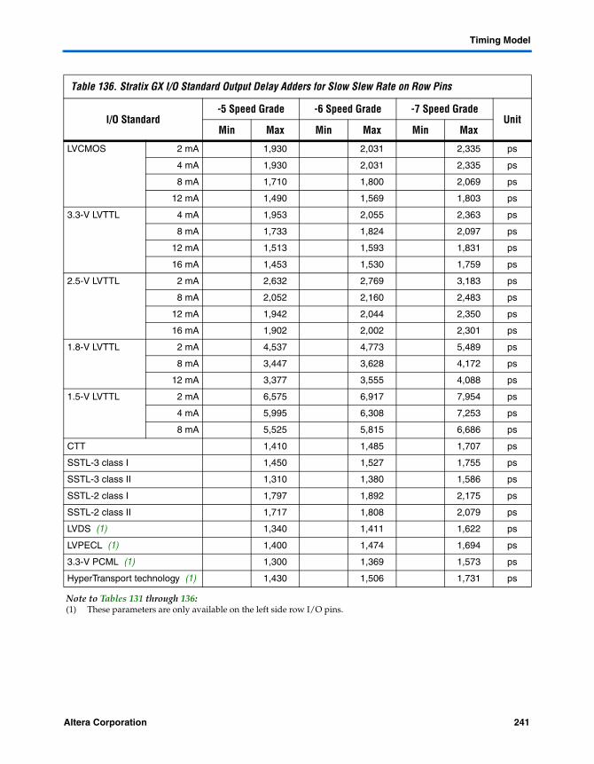
Timing Model
Table 136. Stratix GX I/O Standard Output Delay Adders for Slow Slew Rate on Row Pins
I/O Standard-5 Speed Grade -6 Speed Grade -7 Speed Grade
UnitMin Max Min Max Min Max
LVCMOS 2 mA 1,930 2,031 2,335 ps
4 mA 1,930 2,031 2,335 ps
8 mA 1,710 1,800 2,069 ps
12 mA 1,490 1,569 1,803 ps
3.3-V LVTTL 4 mA 1,953 2,055 2,363 ps
8 mA 1,733 1,824 2,097 ps
12 mA 1,513 1,593 1,831 ps
16 mA 1,453 1,530 1,759 ps
2.5-V LVTTL 2 mA 2,632 2,769 3,183 ps
8 mA 2,052 2,160 2,483 ps
12 mA 1,942 2,044 2,350 ps
16 mA 1,902 2,002 2,301 ps
1.8-V LVTTL 2 mA 4,537 4,773 5,489 ps
8 mA 3,447 3,628 4,172 ps
12 mA 3,377 3,555 4,088 ps
1.5-V LVTTL 2 mA 6,575 6,917 7,954 ps
4 mA 5,995 6,308 7,253 ps
8 mA 5,525 5,815 6,686 ps
CTT 1,410 1,485 1,707 ps
SSTL-3 class I 1,450 1,527 1,755 ps
SSTL-3 class II 1,310 1,380 1,586 ps
SSTL-2 class I 1,797 1,892 2,175 ps
SSTL-2 class II 1,717 1,808 2,079 ps
LVDS (1) 1,340 1,411 1,622 ps
LVPECL (1) 1,400 1,474 1,694 ps
3.3-V PCML (1) 1,300 1,369 1,573 ps
HyperTransport technology (1) 1,430 1,506 1,731 ps
Note to Tables 131 through 136:(1) These parameters are only available on the left side row I/O pins.
Altera Corporation 241Preliminary
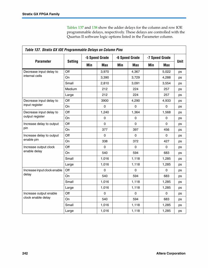
Stratix GX FPGA Family
Tables 137 and 138 show the adder delays for the column and row IOE programmable delays, respectively. These delays are controlled with the Quartus II software logic options listed in the Parameter column.
Table 137. Stratix GX IOE Programmable Delays on Column Pins
Parameter Setting-5 Speed Grade -6 Speed Grade -7 Speed Grade
UnitMin Max Min Max Min Max
Decrease input delay to internal cells
Off 3,970 4,367 5,022 ps
On 3,390 3,729 4,288 ps
Small 2,810 3,091 3,554 ps
Medium 212 224 257 ps
Large 212 224 257 ps
Decrease input delay to input register
Off 3900 4,290 4,933 ps
On 0 0 0 ps
Decrease input delay to output register
Off 1,240 1,364 1,568 ps
On 0 0 0 ps
Increase delay to output pin
Off 0 0 0 ps
On 377 397 456 ps
Increase delay to output enable pin
Off 0 0 0 ps
On 338 372 427 ps
Increase output clock enable delay
Off 0 0 0 ps
On 540 594 683 ps
Small 1,016 1,118 1,285 ps
Large 1,016 1,118 1,285 ps
Increase input clock enable delay
Off 0 0 0 ps
On 540 594 683 ps
Small 1,016 1,118 1,285 ps
Large 1,016 1,118 1,285 ps
Increase output enable clock enable delay
Off 0 0 0 ps
On 540 594 683 ps
Small 1,016 1,118 1,285 ps
Large 1,016 1,118 1,285 ps
242 Altera CorporationPreliminary

Timing Model
Table 138. Stratix GX IOE Programmable Delays on Row Pins
Parameter Setting-5 Speed Grade -6 Speed Grade -7 Speed Grade
UnitMin Max Min Max Min Max
Decrease input delay to internal cells
Off 3,970 4,367 5,022 ps
On 3,390 3,729 4,288 ps
Small 2,810 3,091 3,554 ps
Medium 164 173 198 ps
Large 164 173 198 ps
Decrease input delay to input register
Off 3,900 4,290 4,933 ps
On 0 0 0 ps
Decrease input delay to output register
Off 1,240 1,364 1,568 ps
On 0 0 0 ps
Increase delay to output pin
Off 0 0 0 ps
On 377 397 456 ps
Increase delay to output enable pin
Off 0 0 0 ps
On 348 383 441 ps
Increase output clock enable delay
Off 0 0 0 ps
On 180 198 227 ps
Small 260 286 328 ps
Large 260 286 328 ps
Increase input clock enable delay
Off 0 0 0 ps
On 180 198 227 ps
Small 260 286 328 ps
Large 260 286 328 ps
Increase output enable clock enable delay
Off 0 0 0 ps
On 540 594 683 ps
Small 1,016 1,118 1,285 ps
Large 1,016 1,118 1,285 ps
Altera Corporation 243Preliminary

Stratix GX FPGA Family
The scaling factors for output pin timing in Table 139 are shown in units of time per pF unit of capacitance (ps/pF). Add this delay to the combinational timing path for output or bidirectional pins in addition to the “I/O Adder” delays shown in Tables 131 through 136 and the “IOE Programmable Delays” in Tables 137 and 138.
Table 139. Output Delay Adder for Loading on LVTTL/LVCMOS Output Buffers
LVTTL/LVCMOS Standards
Conditions Output Pin Adder Delay (ps/pF)
Parameter Value 3.3-V LVTTL 2.5-V LVTTL 1.8-V LVTTL 1.5-V LVTTL LVCMOS
Drive Strength
24 mA 15 – – - 8
16 mA 25 18 – – –
12 mA 30 25 25 – 15
8 mA 50 35 40 35 20
4 mA 60 – – 80 30
2 mA – 75 120 160 60
SSTL/HSTL Standards
ConditionsOutput Pin Adder Delay (ps/pF)
SSTL-3 SSTL-2 SSTL-1.8 1.5-V HSTL 1.8-V HSTL
Class IClass II
25 25 25 25 25
25 20 25 20 20
GTL+/GTL/CTT/PCI Standards
Conditions Output Pin Adder Delay (ps/pF)
Parameter Value GTL+ GTL CTT PCI AGP
VC C I O voltage level
3.3 V 18 18 25 20 20
2.5 V 15 18 - - -
244 Altera CorporationPreliminary

Timing Model
Maximum Input & Output Clock Rates
Tables 140 through 142 show the maximum input clock rate for column and row pins in Stratix GX devices.
Table 140. Stratix GX Maximum Input Clock Rate for CLK[7..4] & CLK[15..12] Pins
I/O Standard -5 Speed Grade -6 Speed Grade -7 Speed Grade Unit
LVTTL 422 422 390 MHz
2.5 V 422 422 390 MHz
1.8 V 422 422 390 MHz
1.5 V 422 422 390 MHz
LVCMOS 422 422 390 MHz
GTL 300 250 200 MHz
GTL+ 300 250 200 MHz
SSTL-3 class I 400 350 300 MHz
SSTL-3 class II 400 350 300 MHz
SSTL-2 class I 400 350 300 MHz
SSTL-2 class II 400 350 300 MHz
SSTL-18 class I 400 350 300 MHz
SSTL-18 class II 400 350 300 MHz
1.5-V HSTL class I 400 350 300 MHz
1.5-V HSTL class II 400 350 300 MHz
1.8-V HSTL class I 400 350 300 MHz
1.8-V HSTL class II 400 350 300 MHz
3.3-V PCI 422 422 390 MHz
3.3-V PCI-X 1.0 422 422 390 MHz
Compact PCI 422 422 390 MHz
AGP 1× 422 422 390 MHz
AGP 2× 422 422 390 MHz
CTT 300 250 200 MHz
Differential HSTL 400 350 300 MHz
LVDS 645 645 622 MHz
LVPECL 645 645 622 MHz
PCML 300 275 275 MHz
HyperTransport technology 500 500 450 MHz
Altera Corporation 245Preliminary
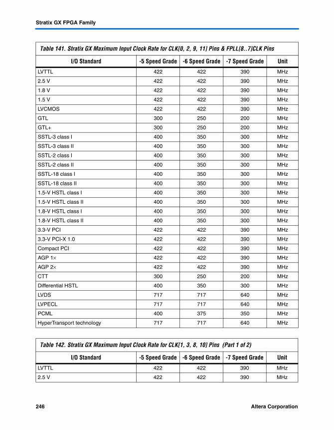
Stratix GX FPGA Family
Table 141. Stratix GX Maximum Input Clock Rate for CLK[0, 2, 9, 11] Pins & FPLL[8..7]CLK Pins
I/O Standard -5 Speed Grade -6 Speed Grade -7 Speed Grade Unit
LVTTL 422 422 390 MHz
2.5 V 422 422 390 MHz
1.8 V 422 422 390 MHz
1.5 V 422 422 390 MHz
LVCMOS 422 422 390 MHz
GTL 300 250 200 MHz
GTL+ 300 250 200 MHz
SSTL-3 class I 400 350 300 MHz
SSTL-3 class II 400 350 300 MHz
SSTL-2 class I 400 350 300 MHz
SSTL-2 class II 400 350 300 MHz
SSTL-18 class I 400 350 300 MHz
SSTL-18 class II 400 350 300 MHz
1.5-V HSTL class I 400 350 300 MHz
1.5-V HSTL class II 400 350 300 MHz
1.8-V HSTL class I 400 350 300 MHz
1.8-V HSTL class II 400 350 300 MHz
3.3-V PCI 422 422 390 MHz
3.3-V PCI-X 1.0 422 422 390 MHz
Compact PCI 422 422 390 MHz
AGP 1× 422 422 390 MHz
AGP 2× 422 422 390 MHz
CTT 300 250 200 MHz
Differential HSTL 400 350 300 MHz
LVDS 717 717 640 MHz
LVPECL 717 717 640 MHz
PCML 400 375 350 MHz
HyperTransport technology 717 717 640 MHz
Table 142. Stratix GX Maximum Input Clock Rate for CLK[1, 3, 8, 10] Pins (Part 1 of 2)
I/O Standard -5 Speed Grade -6 Speed Grade -7 Speed Grade Unit
LVTTL 422 422 390 MHz
2.5 V 422 422 390 MHz
246 Altera CorporationPreliminary

Timing Model
Tables 143 and 144 show the maximum output clock rate for column and row pins in Stratix GX devices.
1.8 V 422 422 390 MHz
1.5 V 422 422 390 MHz
LVCMOS 422 422 390 MHz
GTL 300 250 200 MHz
GTL+ 300 250 200 MHz
SSTL-3 class I 400 350 300 MHz
SSTL-3 class II 400 350 300 MHz
SSTL-2 class I 400 350 300 MHz
SSTL-2 class II 400 350 300 MHz
SSTL-18 class I 400 350 300 MHz
SSTL-18 class II 400 350 300 MHz
1.5-V HSTL class I 400 350 300 MHz
1.5-V HSTL class II 400 350 300 MHz
1.8-V HSTL class I 400 350 300 MHz
1.8-V HSTL class II 400 350 300 MHz
3.3-V PCI 422 422 390 MHz
3.3-V PCI-X 1.0 422 422 390 MHz
Compact PCI 422 422 390 MHz
AGP 1× 422 422 390 MHz
AGP 2× 422 422 390 MHz
CTT 300 250 200 MHz
Differential HSTL 400 350 300 MHz
LVDS 645 645 640 MHz
LVPECL 645 645 640 MHz
PCML 300 275 275 MHz
HyperTransport technology 645 645 640 MHz
Table 142. Stratix GX Maximum Input Clock Rate for CLK[1, 3, 8, 10] Pins (Part 2 of 2)
I/O Standard -5 Speed Grade -6 Speed Grade -7 Speed Grade Unit
Table 143. Stratix GX Maximum Output Clock Rate for PLL[5, 6, 11, 12] Pins (Part 1 of 2)
I/O Standard -5 Speed Grade -6 Speed Grade -7 Speed Grade Unit
LVTTL 350 300 250 MHz
2.5 V 350 300 300 MHz
Altera Corporation 247Preliminary
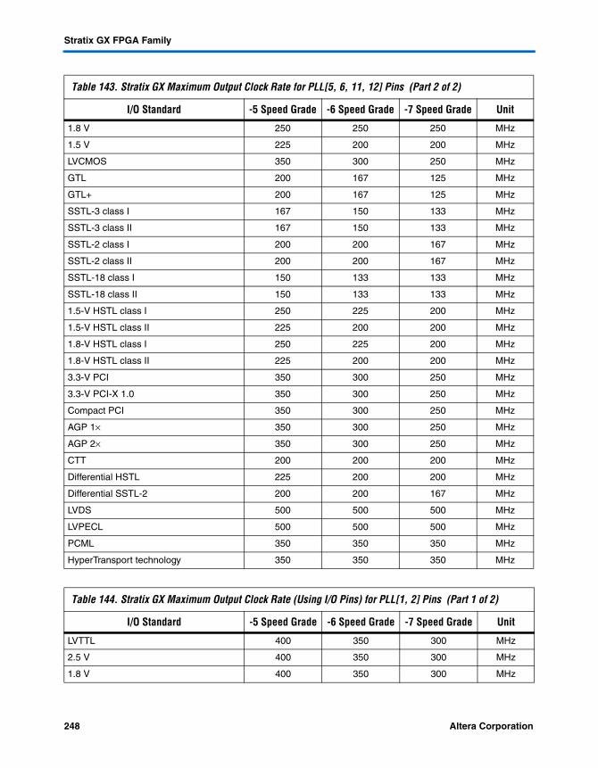
Stratix GX FPGA Family
1.8 V 250 250 250 MHz
1.5 V 225 200 200 MHz
LVCMOS 350 300 250 MHz
GTL 200 167 125 MHz
GTL+ 200 167 125 MHz
SSTL-3 class I 167 150 133 MHz
SSTL-3 class II 167 150 133 MHz
SSTL-2 class I 200 200 167 MHz
SSTL-2 class II 200 200 167 MHz
SSTL-18 class I 150 133 133 MHz
SSTL-18 class II 150 133 133 MHz
1.5-V HSTL class I 250 225 200 MHz
1.5-V HSTL class II 225 200 200 MHz
1.8-V HSTL class I 250 225 200 MHz
1.8-V HSTL class II 225 200 200 MHz
3.3-V PCI 350 300 250 MHz
3.3-V PCI-X 1.0 350 300 250 MHz
Compact PCI 350 300 250 MHz
AGP 1× 350 300 250 MHz
AGP 2× 350 300 250 MHz
CTT 200 200 200 MHz
Differential HSTL 225 200 200 MHz
Differential SSTL-2 200 200 167 MHz
LVDS 500 500 500 MHz
LVPECL 500 500 500 MHz
PCML 350 350 350 MHz
HyperTransport technology 350 350 350 MHz
Table 144. Stratix GX Maximum Output Clock Rate (Using I/O Pins) for PLL[1, 2] Pins (Part 1 of 2)
I/O Standard -5 Speed Grade -6 Speed Grade -7 Speed Grade Unit
LVTTL 400 350 300 MHz
2.5 V 400 350 300 MHz
1.8 V 400 350 300 MHz
Table 143. Stratix GX Maximum Output Clock Rate for PLL[5, 6, 11, 12] Pins (Part 2 of 2)
I/O Standard -5 Speed Grade -6 Speed Grade -7 Speed Grade Unit
248 Altera CorporationPreliminary
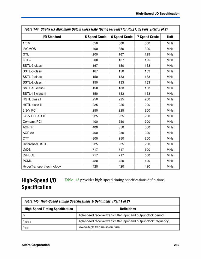
High-Speed I/O Specification
High-Speed I/O Specification
Table 145 provides high-speed timing specifications definitions.
1.5 V 350 300 300 MHz
LVCMOS 400 350 300 MHz
GTL 200 167 125 MHz
GTL+ 200 167 125 MHz
SSTL-3 class I 167 150 133 MHz
SSTL-3 class II 167 150 133 MHz
SSTL-2 class I 150 133 133 MHz
SSTL-2 class II 150 133 133 MHz
SSTL-18 class I 150 133 133 MHz
SSTL-18 class II 150 133 133 MHz
HSTL class I 250 225 200 MHz
HSTL class II 225 225 200 MHz
3.3-V PCI 250 225 200 MHz
3.3-V PCI-X 1.0 225 225 200 MHz
Compact PCI 400 350 300 MHz
AGP 1× 400 350 300 MHz
AGP 2× 400 350 300 MHz
CTT 300 250 200 MHz
Differential HSTL 225 225 200 MHz
LVDS 717 717 500 MHz
LVPECL 717 717 500 MHz
PCML 420 420 420 MHz
HyperTransport technology 420 420 420 MHz
Table 144. Stratix GX Maximum Output Clock Rate (Using I/O Pins) for PLL[1, 2] Pins (Part 2 of 2)
I/O Standard -5 Speed Grade -6 Speed Grade -7 Speed Grade Unit
Table 145. High-Speed Timing Specifications & Definitions (Part 1 of 2)
High-Speed Timing Specification Definitions
tC High-speed receiver/transmitter input and output clock period.
fHSCLK High-speed receiver/transmitter input and output clock frequency.
tRISE Low-to-high transmission time.
Altera Corporation 249Preliminary
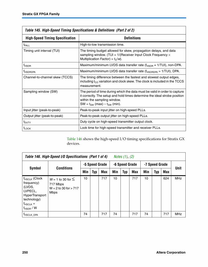
Stratix GX FPGA Family
Table 146 shows the high-speed I/O timing specifications for Stratix GX devices.
tFALL High-to-low transmission time.
Timing unit interval (TUI) The timing budget allowed for skew, propagation delays, and data sampling window. (TUI = 1/(Receiver Input Clock Frequency × Multiplication Factor) = tC/w).
fHSDR Maximum/minimum LVDS data transfer rate (fHSDR = 1/TUI), non-DPA.
fHSDRDPA Maximum/minimum LVDS data transfer rate (fHSDRDPA = 1/TUI), DPA.
Channel-to-channel skew (TCCS) The timing difference between the fastest and slowest output edges, including tCO variation and clock skew. The clock is included in the TCCS measurement.
Sampling window (SW) The period of time during which the data must be valid in order to capture it correctly. The setup and hold times determine the ideal strobe position within the sampling window.SW = tSW (max) – tSW (min).
Input jitter (peak-to-peak) Peak-to-peak input jitter on high-speed PLLs.
Output jitter (peak-to-peak) Peak-to-peak output jitter on high-speed PLLs.
tDUTY Duty cycle on high-speed transmitter output clock.
tLOCK Lock time for high-speed transmitter and receiver PLLs.
Table 145. High-Speed Timing Specifications & Definitions (Part 2 of 2)
High-Speed Timing Specification Definitions
Table 146. High-Speed I/O Specifications (Part 1 of 4) Notes (1), (2)
Symbol Conditions-5 Speed Grade -6 Speed Grade -7 Speed Grade
UnitMin Typ Max Min Typ Max Min Typ Max
fHSCLK (Clock frequency)(LVDS, LVPECL, HyperTransport technology)fHSCLK = fHSDR / W
W = 1 to 30 for ≤ 717 MbpsW = 2 to 30 for > 717 Mbps
10 717 10 717 10 624 MHz
fHSCLK_DPA 74 717 74 717 74 717 MHz
250 Altera CorporationPreliminary

High-Speed I/O Specification
fHSDR Device operation(LVDS, LVPECL, HyperTransport technology)
J = 10 300 840 300 840 300 840 Mbps
J = 8 300 840 300 840 300 840 Mbps
J = 7 300 840 300 840 300 840 Mbps
J = 4 300 840 300 840 300 840 Mbps
J = 2 100 624 100 624 100 462 Mbps
J = 1 (LVDS and LVPECL only)
100 462 100 462 100 462 Mbps
fHSDRDPA (LVDS, LVPECL)
J=10 300 1000 300 840 300 840 Mbps
J=8 300 1000 300 840 300 840 Mbps
fHSCLK (Clock frequency)(PCML)fHSCLK =fHSDR / W
W = 1 to 30 10 400 10 400 10 311 MHz
fHSDR Device operation (PCML)
J = 10 300 400 300 400 300 311 Mbps
J = 8 300 400 300 400 300 311 Mbps
J = 7 300 400 300 400 300 311 Mbps
J = 4 300 400 300 400 300 311 Mbps
J = 2 100 400 100 400 100 300 Mbps
J = 1 100 250 100 250 100 200 Mbps
DPA Run Length
6400 6400 6400 UI
DPA Jitter Tolerance(p-p)
all data rates 0.44 0.44 0.44 UI
DPA Minimum Eye opening (p-p)
0.56 0.56 0.56 UI
DPA Receiver Latency
5 9 5 9 5 9 Number of
parallel CLK
cycles
Table 146. High-Speed I/O Specifications (Part 2 of 4) Notes (1), (2)
Symbol Conditions-5 Speed Grade -6 Speed Grade -7 Speed Grade
UnitMin Typ Max Min Typ Max Min Typ Max
Altera Corporation 251Preliminary

Stratix GX FPGA Family
DPA Lock Time Stan-dard
Train-ing Pat-tern
Trans-ition Den-sity
SPI-4, CSIX
00000000001111111111
10% 256 256 256 Number of
repet-itions
Rapid IO
00001111
25% 256 256 256 Number of
repet-itions
10010000
50% 256 256 256 Number of
repet-itions
Misc 10101010
100% 256 256 256 Number of
repet-itions
01010101
256 256 256 Number of
repet-itions
TCCS All 200 200 300 ps
SW PCML (J = 4, 7, 8, 10)
750 750 800 ps
PCML (J = 2) 900 900 1,200 ps
PCML (J = 1) 1,500
1,500 1,700 ps
LVDS and LVPECL (J = 1)
500 500 550 ps
LVDS, LVPECL, HyperTransport technology (J = 2 through 10)
440 440 500 ps
Input jitter tolerance (peak-to-peak)
All 250 250 250 ps
Table 146. High-Speed I/O Specifications (Part 3 of 4) Notes (1), (2)
Symbol Conditions-5 Speed Grade -6 Speed Grade -7 Speed Grade
UnitMin Typ Max Min Typ Max Min Typ Max
252 Altera CorporationPreliminary

High-Speed I/O Specification
Output jitter (peak-to-peak)
All 160 160 200 ps
Output tRISE LVDS 80 110 120 80 110 120 80 110 120 ps
HyperTransport technology
110 170 200 110 170 200 120 170 200 ps
LVPECL 90 130 150 90 130 150 100 135 150 ps
PCML 80 110 135 80 110 135 80 110 135 ps
Output tFALL LVDS 80 110 120 80 110 120 80 110 120 ps
HyperTransport technology
110 170 200 110 170 200 110 170 200 ps
LVPECL 90 130 160 90 130 160 100 135 160 ps
PCML 105 140 175 105 140 175 110 145 175 ps
tDUTY LVDS (J = 2 through 10)
47.5 50 52.5 47.5 50 52.5 47.5 50 52.5 %
LVDS (J =1) and LVPECL, PCML, HyperTransport technology
45 50 55 45 50 55 45 50 55 %
tLOCK All 100 100 100 µs
Notes to Table 146:(1) When J = 4, 7, 8, and 10, the SERDES block is used.(2) When J = 2 or J = 1, the SERDES is bypassed.
Table 146. High-Speed I/O Specifications (Part 4 of 4) Notes (1), (2)
Symbol Conditions-5 Speed Grade -6 Speed Grade -7 Speed Grade
UnitMin Typ Max Min Typ Max Min Typ Max
Altera Corporation 253Preliminary

Stratix GX FPGA Family
PLL Timing
Tables 147 through 149 describe the Stratix GX device enhanced PLL specifications.
Table 147. Enhanced PLL Specifications for -5 Speed Grades (Part 1 of 2)
Symbol Parameter Min Typ Max Unit
fIN Input clock frequency 3 (1) 684 MHz
fINDUTY Input clock duty cycle 40 60 %
fEINDUTY External feedback clock input duty cycle
40 60 %
tINJITTER Input clock period jitter ±200 (2) ps
tEINJITTER External feedback clock period jitter ±200 (2) ps
tFCOMP External feedback clock compensation time (3)
6 ns
fOUT Output frequency for internal global or regional clock
0.3 500 MHz
fOUT_EXT Output frequency for external clock (2) 0.3 526 MHz
tOUTDUTY Duty cycle for external clock output (when set to 50%)
45 55 %
tJITTER Period jitter for external clock output (5) ±100 ps for >200 MHz outclk±20 mUI for <200 MHz outclk
ps or mUI
tCONFIG5,6 Time required to reconfigure the scan chains for PLLs 5 and 6
289/fSCANCLK
tCONFIG11,12 Time required to reconfigure the scan chains for PLLs 11 and 12
193/fSCANCLK
tSCANCLK scanclk frequency (4) 22 MHz
tDLOCK Time required to lock dynamically (after switchover or reconfiguring any non-post-scale counters/delays) (6)
100 µs
tLOCK Time required to lock from end of device configuration
10 400 µs
fVCO PLL internal VCO operating range 300 800 (7) MHz
tLSKEW Clock skew between two external clock outputs driven by the same counter
±50 ps
tSKEW Clock skew between two external clock outputs driven by the different counters with the same settings
±75 ps
fSS Spread spectrum modulation frequency 30 150 kHz
254 Altera CorporationPreliminary

High-Speed I/O Specification
% spread Percentage spread for spread spectrum frequency (9)
0.4 0.5 0.6 %
tARESET Minimum pulse width on areset signal
10 ns
Table 148. Enhanced PLL Specifications for -6 Speed Grades (Part 1 of 2)
Symbol Parameter Min Typ Max Unit
fIN Input clock frequency 3 (1) 650 MHz
fINDUTY Input clock duty cycle 40 60 %
fEINDUTY External feedback clock input duty cycle
40 60 %
tINJITTER Input clock period jitter ±200 (2) ps
tEINJITTER External feedback clock period jitter ±200 (2) ps
tFCOMP External feedback clock compensation time (3)
6 ns
fOUT Output frequency for internal global or regional clock
0.3 450 MHz
fOUT_EXT Output frequency for external clock (2) 0.3 500 MHz
tOUTDUTY Duty cycle for external clock output (when set to 50%)
45 55 %
tJITTER Period jitter for external clock output (5) ±100 ps for >200 MHz outclk±20 mUI for <200 MHz outclk
ps or mUI
tCONFIG5,6 Time required to reconfigure the scan chains for PLLs 5 and 6
289/fSCANCLK
tCONFIG11,12 Time required to reconfigure the scan chains for PLLs 11 and 12
193/fSCANCLK
tSCANCLK scanclk frequency (4) 22 MHz
tDLOCK Time required to lock dynamically (after switchover or reconfiguring any non-post-scale counters/delays) (6) (10)
(8) 100 µs
tLOCK Time required to lock from end of device configuration (10)
10 400 µs
fVCO PLL internal VCO operating range 300 800 (7) MHz
tLSKEW Clock skew between two external clock outputs driven by the same counter
±50 ps
Table 147. Enhanced PLL Specifications for -5 Speed Grades (Part 2 of 2)
Symbol Parameter Min Typ Max Unit
Altera Corporation 255Preliminary

Stratix GX FPGA Family
tSKEW Clock skew between two external clock outputs driven by the different counters with the same settings
±75 ps
fSS Spread spectrum modulation frequency 30 150 kHz
% spread Percentage spread for spread spectrum frequency (9)
0.4 0.5 0.6 %
tARESET Minimum pulse width on areset signal
10 ns
Table 149. Enhanced PLL Specifications for -7 Speed Grade (Part 1 of 2)
Symbol Parameter Min Typ Max Unit
fIN Input clock frequency 3 (1) 565 MHz
fINDUTY Input clock duty cycle 40 60 %
fEINDUTY External feedback clock input duty cycle
40 60 %
tINJITTER Input clock period jitter ±200 (2) ps
tEINJITTER External feedback clock period jitter ±200 (2) ps
tFCOMP External feedback clock compensation time (3)
6 ns
fOUT Output frequency for internal global or regional clock
0.3 420 MHz
fOUT_EXT Output frequency for external clock (2) 0.3 434 MHz
tOUTDUTY Duty cycle for external clock output (when set to 50%)
45 55 %
tJITTER Period jitter for external clock output (5) ±100 ps for >200 MHz outclk±20 mUI for <200 MHz outclk
ps or mUI
tCONFIG5,6 Time required to reconfigure the scan chains for PLLs 5 and 6
289/fSCANCLK
tCONFIG11,12 Time required to reconfigure the scan chains for PLLs 11 and 12
193/fSCANCLK
tSCANCLK scanclk frequency (4) 22 MHz
tDLOCK Time required to lock dynamically (after switchover or reconfiguring any non-post-scale counters/delays) (6) (10)
(8) 100 µs
tLOCK Time required to lock from end of device configuration (10)
10 400 µs
fVCO PLL internal VCO operating range 300 600 (7) MHz
Table 148. Enhanced PLL Specifications for -6 Speed Grades (Part 2 of 2)
Symbol Parameter Min Typ Max Unit
256 Altera CorporationPreliminary

High-Speed I/O Specification
tLSKEW Clock skew between two external clock outputs driven by the same counter
±50 ps
tSKEW Clock skew between two external clock outputs driven by the different counters with the same settings
±75 ps
fSS Spread spectrum modulation frequency 30 150 kHz
% spread Percentage spread for spread spectrum frequency (9)
0.5 0.6 %
tARESET Minimum pulse width on areset signal
10 ns
Notes to Tables 147 through 149:(1) The minimum input clock frequency to the PFD (fIN/N) must be at least 3 MHz for Stratix device enhanced PLLs.(2) See “Maximum Input & Output Clock Rates” on page 245.(3) tFCOMP can also equal 50% of the input clock period multiplied by the pre-scale divider n (whichever is less).(4) This parameter is timing analyzed by the Quartus II software because the scanclk and scandata ports can be
driven by the logic array.(5) Actual jitter performance may vary based on the system configuration.(6) Total required time to reconfigure and lock is equal to tDLOCK + tCONFIG. If only post-scale counters and delays are
changed, then tDLOCK is equal to 0.(7) The VCO range is limited to 500 to 800 MHz when the spread spectrum feature is selected.(8) Lock time is a function of PLL configuration and may be significantly faster depending on bandwidth settings or
feedback counter change increment.(9) Exact, user-controllable value depends on the PLL settings.(10) The LOCK circuit on Stratix PLLs does not work for industrial devices below -20C unless the PFD frequency > 200
MHz. See the Stratix FPGA Errata Sheet for more information on the PLL.
Table 149. Enhanced PLL Specifications for -7 Speed Grade (Part 2 of 2)
Symbol Parameter Min Typ Max Unit
Altera Corporation 257Preliminary

Stratix GX FPGA Family
Table 150 describes the Stratix GX device fast PLL specifications.
Table 150. Fast PLL Specifications for -5 & -6 Speed Grade Devices
Symbol Parameter Min Max Unit
fIN CLKIN frequency (for m = 1) (1) 300 717 MHz
CLKIN frequency (for m = 2 to 19) 300/m
1,000/m MHz
CLKIN frequency (for m = 20 to 32) 10 1,000/m MHz
fOUT Output frequency for internal global or regional clock (2)
9.4 420 MHz
fOUT_EXT Output frequency for external clock 9.375 717 MHz
fVCO VCO operating frequency 300 1,000 MHz
tINDUTY CLKIN duty cycle 40 60 %
tINJITTER Period jitter for CLKIN pin ±200 ps
tDUTY Duty cycle for DFFIO 1× CLKOUT pin (3) 45 55 %
tJITTER Period jitter for DIFFIO clock out (3) ±80 ps
Period jitter for internal global or regional clock
±100 ps for >200-MHz outclk±20 mUI for <200-MHz outclk
ps or mUI
tLOCK Time required for PLL to acquire lock 10 100 µs
m Multiplication factors for m counter (3) 1 32 Integer
l0, l1, g0 Multiplication factors for l0, l1, and g0 counter (4), (5)
1 32 Integer
tARESET Minimum pulse width on areset signal
10 ns
Table 151. Fast PLL Specifications for -7 & -8 Speed Grades (Part 1 of 2)
Symbol Parameter Min Max Unit
fIN CLKIN frequency (for m = 1) (1), 300 640 MHz
CLKIN frequency (for m = 2 to 19) 300/m
700/m MHz
CLKIN frequency (for m = 20 to 32) 10 700/m MHz
fOUT Output frequency for internal global or regional clock (2)
9.375 420 MHz
fOUT_EXT Output frequency for external clock 9.4 500 MHz
fVCO VCO operating frequency 300 700 MHz
tINDUTY CLKIN duty cycle 40 60 %
tINJITTER Period jitter for CLKIN pin ±200 ps
258 Altera CorporationPreliminary

DLL Jitter
DLL Jitter Table 152 reports the jitter for the DLL in the DQS phase shift reference circuit.
For more information on DLL jitter, see the DDR SRAM section in the Stratix Architecture chapter in the Stratix Device Handbook, Volume 1.
Software Stratix GX devices are supported by the Altera Quartus II design software, which provides a comprehensive environment for system-on-a-programmable-chip (SOPC) design. The Quartus II software includes hardware description language and schematic design entry, compilation and logic synthesis, full simulation and advanced timing analysis,
tDUTY Duty cycle for DFFIO 1× CLKOUT pin (3) 45 55 %
tJITTER Period jitter for DIFFIO clock out (3) ±80 ps
Period jitter for internal global or regional clock
±100 ps for >200 MHz outclk±20 mUI for <200 MHz outclk
ps or mUI
tLOCK Time required for PLL to acquire lock 10 100 µs
m Multiplication factors for m counter (4) 1 32 Integer
l0, l1, g0 Multiplication factors for l0, l1, and g0 counter (4), (5)
1 32 Integer
tARESET Minimum pulse width on areset signal
10 ns
Notes to Tables 150 and 151:(1) See “Maximum Input & Output Clock Rates” on page 245.(2) When using the SERDES, high-speed differential I/O mode supports a maximum output frequency of 210 MHz
to the global or regional clocks (i.e., the maximum data rate 840 Mbps divided by the smallest SERDES J factor of 4).
(3) This parameter is for high-speed differential I/O mode only.(4) These counters have a maximum of 32 if programmed for 50/50 duty cycle. Otherwise, they have a maximum
of 16. (5) High-speed differential I/O mode supports W = 1 to 16 and J = 4, 7, 8, or 10.
Table 151. Fast PLL Specifications for -7 & -8 Speed Grades (Part 2 of 2)
Symbol Parameter Min Max Unit
Table 152. DLL Jitter for DQS Phase Shift Reference Circuit
Frequency (MHz) DLL Jitter (ps)
197 to 200 ± 100
160 to 196 ± 300
100 to 159 ± 500
Altera Corporation 259Preliminary

Stratix GX FPGA Family
SignalTap logic analysis, and device configuration. See the Design Software Selector Guide for more details on the Quartus II software features.
The Quartus II software supports the Windows 2000/NT/98, Sun Solaris, Linux Red Hat v6.2 and HP-UX operating systems. It also supports seamless integration with industry-leading EDA tools through the NativeLink® interface.
Device Pin-Outs Device pin-outs for Stratix GX devices will be released on the Altera web site (www.altera.com).
Ordering Information
Ordering information will be available in a future version of this data sheet.
Revision History The information contained in the Stratix GX FPGA Family data sheet version 2.2 supersedes information published in previous versions.
Version 2.2
The following changes were made to the Stratix GX FPGA Family data sheet version 2.2:
Updated Figures 37, 38, and 125. Updated Tables 61, 66, 102, 109, 140, 141, and 143. Updated the section “Phase Compensation FIFO Buffer” on page 31. Updated the section “Logic Array Blocks” on page 61. Updated the section “Clock Switchover” on page 144. Updated the section “Lock Detect” on page 152. Updated the section “Advanced Clear & Enable Control” on
page 153. Updated the section “I/O Structure” on page 157. Updated the section “Power Sequencing & Hot Socketing” on
page 182. Removed Txz, Tzx, Tzxpll, and Txzpll parameters because of errors
in data. These parameters will be added in when new data is available.
Version 2.1
The following changes were made to the Stratix GX FPGA Family data sheet version 2.1:
260 Altera CorporationPreliminary

Revision History
Updated “Transceiver Blocks” section. Added “Stratix GX Clocking” section. Updated “Source-Synchronous Signaling with DPA” section. Updated termination information. Updated Figure 63. Updated timing parameters. Added Stratix GX transceiver parameters. Updated Gigabit Ethernet support information.
Altera Corporation 261Preliminary

Stratix GX FPGA Family
262 Altera CorporationPreliminary