STL2 Server Board - BLTP JINR Home Pagetheor.jinr.ru/guide/tfs/stl2_tps.pdf · STL2 Server Board...
113
STL2 Server Board Technical Product Specification Intel Order Number A44368-002 Revision 1.1 December 27, 2000 Enterprise Platforms Group
Transcript of STL2 Server Board - BLTP JINR Home Pagetheor.jinr.ru/guide/tfs/stl2_tps.pdf · STL2 Server Board...

STL2 Server Board
Technical Product Specification
Intel Order Number A44368-002
Revision 1.1
December 27, 2000
Enterprise Platforms Group
Revision History STL2 Server Board TPS
Revision 1.1 ii
Revision History Date Revision
Number Modifications
6/15/00 0.5 Initial release.
6/20/00 0.6 Updated connector reference designators
7/7/00 0.61 Updated silkscreen reference designators to agree with STL2 FAB2. Removed figure 2-3, IB6566 IRQ routing diagram. Added BIOS recovery jumper information. Corrected grammar / spelling errors. Updated table 5-1, STL2 Hardware Sensors, per recent information
8/24/00 0.7 Updated Section 5: Jumpers and Connectors, per modifications to the STL2 Fab3 Silver boards. Updated Section 4.2: BIOS Setup, per modifications included in BIOS Release 1.1. Added power consumption information to Section 6.
9/22/00 1.0 Released version
12/27/00 1.1 Added estimated MTBF calculation for the STL2 and absolute maximum ratings to Section 6. Added note to Section 5.2.1.4 that i t is not necessary to set the jumpers on the processor frequency jumper block 5E1 when using production level (SL Spec) processors. Modified step # 4 of Section 5.2.1.3 Performing a BIOS Recovery Boot.
Disclaimers
Information in this document is provided in connection with Intel® products. No license, express or implied, by estoppel or otherwise, to any intellectual property rights is granted by this document. Except as provided in Intel's Terms and Conditions of Sale for such products, Intel assumes no liability whatsoever, and Intel disclaims any express or implied warranty, relating to sale and/or use of Intel products including liability or warranties relating to fitness for a particular purpose, merchantability, or infringement of any patent, copyright or other intellectual property right. Intel products are not intended for use in medical, life saving, or life sustaining applications. Intel may make changes to specifications and product descriptions at any time, without notice.
Designers must not rely on the absence or characteristics of any features or instructions marked "reserved" or "undefined." Intel reserves these for future definition and shall have no responsibility whatsoever for conflicts or incompatibilities arising from future changes to them.
This document contains information on products in the design phase of development. Do not finalize a design with this information. Revised information will be published when the product is available. Verify with your local sales office that you have the latest datasheet before finalizing a design.
The STL2 platform may contain design defects or errors known as errata which may cause the product to deviate from published specifications. Current characterized errata are available on request.
Copyright © Intel Corporation 2000- 2001. *Other brands and names are the property of their respective owners.
STL2 Server Board TPS Table of Contents
Revision 1.1
iii
Table of Contents
1. Introduction......................................................................................................................1-1
1.1 Purpose .........................................................................................................................1-1
1.2 Audience........................................................................................................................1-1
1.3 STL2 Server Board Feature Overview.......................................................................1-1
1.4 STL2 Server Board Block Diagram ...........................................................................1-2
2. STL2 Server Board Architecture Overview..............................................................2-3
2.1 Intel® Pentium® III Processor Subsystem..................................................................2-3
2.1.1 Supported Processor Types.................................................................................2-3
2.1.2 Dual Processor Operation.....................................................................................2-4
2.1.3 PGA370 Socket .....................................................................................................2-4
2.1.4 Processor Bus Termination / Regulation / Power...............................................2-4
2.1.5 Termination Package.............................................................................................2-4
2.1.6 APIC Bus.................................................................................................................2-4
2.1.7 Boxed Processors..................................................................................................2-4
2.2 ServerWorks ServerSet III LE Chipset.......................................................................2-5
2.3 Memory..........................................................................................................................2-5
2.4 PCI I/O Subsystem........................................................................................................2-6
2.4.1 64-bit / 66 MHz PCI Subsystem............................................................................2-6
2.4.2 32-bit/33 MHz PCI Subsystem..............................................................................2-8
2.5 Chipset Support Components...................................................................................2-13
2.5.1 Legacy I/O (Super I/O) National* PC97317VUL ...............................................2-13
2.5.2 BIOS Flash............................................................................................................2-15

Table of Contents STL2 Server Board TPS
Revision 1.1 iv
2.5.3 External Device Connectors................................................................................2-15
2.6 Interrupt Routing ..........................................................................................................2-15
2.6.1 Default I/O APIC....................................................................................................2-15
2.6.2 Extended I/O APIC ...............................................................................................2-15
2.6.3 PCI Ids ...................................................................................................................2-18
2.6.4 Relationship between PCI IRQ and PCI Device ...............................................2-18
3. Server Management.....................................................................................................3-21
3.1 Baseboard Management Controller .........................................................................3-21
3.2 Hardware Sensors......................................................................................................3-22
3.3 ACPI.............................................................................................................................3-26
3.4 AC Link Mode .............................................................................................................3-26
3.5 Wake On LAN Function.............................................................................................3-27
4. Basic Input Output System (BIOS)...........................................................................4-29
4.1 BIOS Overview............................................................................................................4-29
4.1.1 System BIOS.........................................................................................................4-30
4.1.2 Flash Update Utility ..............................................................................................4-30
4.2 Setup Utility..................................................................................................................4-31
4.2.1 Configuration Utilities Overview..........................................................................4-31
4.2.2 Setup Utility Operation.........................................................................................4-31
4.3 CMOS Memory Definition..........................................................................................4-43
4.4 CMOS Default Override.............................................................................................4-43
4.5 Flash Update Utility.....................................................................................................4-43
4.5.1 Loading the System BIOS ...................................................................................4-44
4.5.2 OEM Customization.............................................................................................4-44
4.5.3 Language Area.....................................................................................................4-48

STL2 Server Board TPS Table of Contents
Revision 1.1
v
4.5.4 Recovery Mode.....................................................................................................4-48
4.6 Error Messages and Error Codes ............................................................................4-48
4.6.1 POST Codes ........................................................................................................4-48
4.6.2 POST Error Codes and Messages....................................................................4-53
4.7 Identifying BIOS and BMC Revision Levels .............................................................4-56
4.7.1 BIOS Revision Level Identification......................................................................4-56
4.7.2 BMC Revision Level Identification......................................................................4-56
4.8 Adaptec SCSI Utility...................................................................................................4-56
4.8.1 Running the SCSI Utility.......................................................................................4-57
4.8.2 Adaptec SCSI Utility Configuration Settings .....................................................4-57
4.8.3 Exiting Adaptec SCSI Utility................................................................................4-59
5. Jumpers and Connectors ..........................................................................................5-61
5.1 STL2 Server Board Jumper and Connector Locations..........................................5-61
5.2 Jumper Blocks ............................................................................................................5-63
5.2.1 Setting CMOS/Password Clear Jumper Block 1J15.......................................5-63
5.2.2 Setting Configuration Jumper Block 1L4...........................................................5-67
5.2.3 Setting Configuration Jumper Block 6A.............................................................5-67
5.3 Connectors ..................................................................................................................5-67
5.3.1 Main ATX Power Connector (P33).....................................................................5-68
5.3.2 Auxilary ATX Power Connector (P34)................................................................5-68
5.3.3 I2C Power Connector (P37).................................................................................5-68
5.3.4 System Fan Connectors (P29, P27, P11).........................................................5-69
5.3.5 Processor Connectors (P12, P36).....................................................................5-69
5.3.6 Speaker Connector (P31) ...................................................................................5-69
5.3.7 Speaker Connector (P25) ...................................................................................5-69
Table of Contents STL2 Server Board TPS
Revision 1.1 vi
5.3.8 Diskette Drive Connector (P20) .........................................................................5-70
5.3.9 SVGA Video Port.................................................................................................5-70
5.3.10 Keyboard and Mouse Connectors ...................................................................5-71
5.3.11 Parallel Port ........................................................................................................5-71
5.3.12 Serial Ports COM1 and COM2.........................................................................5-72
5.3.13 RJ-45 LAN Connector .......................................................................................5-72
5.3.14 USB Connectors ................................................................................................5-72
5.3.15 Ultra SCSI Connector (P9)................................................................................5-73
5.3.16 Ultra160 SCSI Connector (P8) .........................................................................5-73
5.3.17 IDE Connector (P19) .........................................................................................5-74
5.3.18 32-Bit PCI Connector.........................................................................................5-75
5.3.19 64-Bit PCI Connector.........................................................................................5-76
5.3.20 Front Panel 24-pin Connector Pinout (P23)....................................................5-77
6. Baseboard Specifications..........................................................................................6-81
6.1 Estimated Baseboard MTBF....................................................................................6-81
6.2 Absolute Maximum Ratings.......................................................................................6-82
6.3 Calculated Power Consumption ...............................................................................6-82
6.4 Measured Power Consumption ................................................................................6-83
6.5 Mechanical Specifications.........................................................................................6-84
7. Regulatory and Integration Information .................................................................7-87
7.1 Regulatory Compliance..............................................................................................7-87
7.2 Installation Instructions................................................................................................7-88
7.2.1 Ensure EMC..........................................................................................................7-88
7.2.2 Ensure Host Computer and Accessory Module Certifications........................7-89
7.2.3 Prevent Power Supply Overload.........................................................................7-89

STL2 Server Board TPS Table of Contents
Revision 1.1
vii
7.2.4 Place Battery Marking on Computer ..................................................................7-89
7.2.5 Use Only for Intended Applications.....................................................................7-90
7.2.6 Installation Precautions ........................................................................................7-90
8. Errata Listing .................................................................................................................8-91
8.1 Summary Errata Table ...............................................................................................8-91
8.1.1 Codes Used in Summary Table..........................................................................8-91
8.2 Errata ...........................................................................................................................8-91
Appendix A: Glossary ...............................................................................................................i
Appendix B: Reference Documents ...................................................................................III
List of Figures STL2 Server Board TPS
Revision 1.1 viii
List of Figures
Figure 1-1. STL2 Server Board Block Diagram.....................................................................1-2
Figure 2-1. Embedded NIC PCI Signals .................................................................................2-9
Figure 2-2. Video Controller PCI Signals ..............................................................................2-10
Figure 2-3. STL2 Baseboard Interrupt Routing Diagram (PIC mode) ...............................2-16
Figure 2-4. STL2 Baseboard Interrupt Routing Diagram (Symmetric mode) ...................2-17
Figure 5-1. STL2 Server Board Jumper and Connector Locations ...................................5-61
Figure 5-2. I/O Back Panel Connectors.................................................................................5-62
Figure 5-3. STL2 Jumper Locations ......................................................................................5-63
Figure 5-4. Diskette Drive Connector Pin Diagram.............................................................5-70
Figure 5-5. IDE Connector Pin Diagram...............................................................................5-74

List of Tables STL2 Server Board TPS
Revision 1.1 x
List of Tables
Table 2-1. STL2 Server Board Supported Processors .........................................................2-3
Table 2-2. SCSI Transfer Speeds............................................................................................2-7
Table 2-3. Embedded SCSI Supported PCI Commands .....................................................2-7
Table 2-4. Video Controller Supported PCI Commands.....................................................2-11
Table 2-5. Standard VGA Modes...........................................................................................2-11
Table 2-6. STL2 PCI IDs .........................................................................................................2-18
Table 2-7. STL2 Relationship between PCI IRQ and PCI Device......................................2-18
Table 3-1. STL2 Hardware Sensors ......................................................................................3-22
Table 3-2. STL2 Supported System Event Log (SEL) events ............................................3-23
Table 4-1. Setup Utility Screen...............................................................................................4-31
Table 4-2. Main Menu Selections...........................................................................................4-34
Table 4-3. Primary Master and Slave Adapters Submenu Selections...............................4-35
Table 4-4. Processor Settings Submenu Selections ...........................................................4-35
Table 4-5. Advanced Menu Selections..................................................................................4-36
Table 4-6. Memory Reconfiruation Submenu Selections ....................................................4-36
Table 4-7. Peripheral Configuration Submenu Selections ..................................................4-37
Table 4-8. PCI Device Submenu Selections.........................................................................4-38
Table 4-9. Option ROM Submenu Selections.......................................................................4-38
Table 4-10. Numlock Submenu Selections ...........................................................................4-39
Table 4-11. Security Menu Selections ...................................................................................4-39
Table 4-12. Secure Mode Submenu Selections...................................................................4-40
Table 4-13. Server Menu Selections......................................................................................4-40
Table 4-14. Wake On Events Submenu Selections .............................................................4-41
Table 4-15. Console Redirection Submenu Selections.......................................................4-41
Table 4-16. Boot Menu Selections.........................................................................................4-41
Table 4-17. Boot Device Priority Selections .........................................................................4-42
Table 4-18. Hard Drive Selections .........................................................................................4-42
Table 4-19. Removable Devices Selections.........................................................................4-42
Table 4-20. Exit Menu Selections...........................................................................................4-43

STL2 Server Board TPS List of Tables
Revision 1.1
xi
Table 4-21. User Binary Area Scan Point Definitions..........................................................4-47
Table 4-22. Format of the User Binary Information Structure..............................................4-47
Table 4-23. Port-80h Code Definition....................................................................................4-49
Table 4-24. Standard BIOS Port-80 Codes..........................................................................4-49
Table 4-25. Recovery BIOS Port-80 Codes..........................................................................4-52
Table 4-26. POST Error Messages and Codes...................................................................4-53
Table 4-27. POST Error Conditions and Beep Codes........................................................4-55
Table 4-28. Channel Configuration........................................................................................4-57
Table 4-29. Adapter Selection Options .................................................................................4-57
Table 4-30. Active Keys for SCSI Utility Screens.................................................................4-57
Table 4-31. Adaptec SCSI Utility Setup Configurations ......................................................4-58
Table 5-1. Jumper Block 1J15 Settings ................................................................................5-64
Table 5-2. Jumper Block 5E1 Settings..................................................................................5-66
Table 5-3. Jumper Block 1J15 Default Settings ...................................................................5-66
Table 5-4. Jumper Block 1L4 Settings ..................................................................................5-67
Table 5-5. Jumper Block 6A Settings ....................................................................................5-67
Table 5-6. Main ATX Power Connector Pinout.....................................................................5-68
Table 5-7. Auxiliary ATX Power Connector Pinout...............................................................5-68
Table 5-8. I2C Power Connector Pinout.................................................................................5-68
Table 5-9. Board Fan Connector Pinout................................................................................5-69
Table 5-10. Processor Fan Connector Pinout ......................................................................5-69
Table 5-11. Speaker Connector Pinout.................................................................................5-69
Table 5-12. Speaker Connector Pinout.................................................................................5-69
Table 5-13. Diskette Drive Connector Pinout .......................................................................5-70
Table 5-14. Video Port Connector Pinout .............................................................................5-70
Table 5-15. Keyboard and Mouse Connector Pinouts.........................................................5-71
Table 5-16. Parallel Port Connector Pinouts.........................................................................5-71
Table 5-17. Serial Ports COM1 and COM2 Connector Pinouts.........................................5-72
Table 5-18. RJ-45 LAN Connector Signals...........................................................................5-72
Table 5-19. USB Connectors..................................................................................................5-72
Table 5-20. Ultra SCSI Connector Pinout..............................................................................5-73
Table 5-21. Ultra160 SCSI Connector...................................................................................5-73

List of Tables STL2 Server Board TPS
Revision 1.1 xii
Table 5-22. IDE Connector Pinout .........................................................................................5-74
Table 5-23. 32-Bit PCI Connector Pinout..............................................................................5-75
Table 5-24. 64-Bit PCI Connctor Pinout................................................................................5-76
Table 5-25. Front Panel 24-pin Connector Pinout................................................................5-77
Table 6-1. Estimated MTBF Calculated Numbers for STL2 ...............................................6-81
Table 6-2. Absolute Maximum Ratings..................................................................................6-82
Table 6-3. STL2 Server Board Calculated Power Consumption........................................6-82
Table 6-4. STL2 Server Board Measured Power Consumption.........................................6-83
Table 7-1. Safety Regulations.................................................................................................7-87
Table 7-2. EMC Regulations...................................................................................................7-87

STL2 Server Board TPS Introduction
Revision 1.1
1-1
1. Introduction
1.1 Purpose This document provides an architectural overview of the STL2 server board, including the board layout of major components and connectors, and an overview of the server board’s feature set.
1.2 Audience This document is written for technical personnel who want a technical overview of the STL2 server board. Familiarity with the personal computer, Intel server architecture and the Peripheral Component Interconnect (PCI) local bus architecture is assumed.
1.3 STL2 Server Board Feature Overview The STL2 server board provides the following features:
• Dual Intel® Pentium® III processor support - Support for one or two identical Intel Pentium III processors for the PGA370 socket,
which utilizes a new package technology called the Flip Chip Pin Grid Array (FC-PGA) package
- One embedded Voltage Regulating Module (VRM) for support of the primary processor, and one VRM connector for support of the secondary processor
• ServerWorks* ServerSet* III LE chipset - 133-MHz Front Side Bus (FSB) Capability - NB6635 North Bridge 3.0 LE - IB6566 South Bridge
• Support for four 3.3-V, registered ECC SDRAM DIMMs that are compliant with the JEDEC PC133 specification - Support for DIMM sizes 64 MB to 1 GB. Four DIMM slots allow a maxiumum installed
memory of 4 GBs - ECC single-bit correction, and multiple-bit detection
• 64-bit, 66-MHz, 3.3-V keyed PCI segment with two expansion connectors and one embedded device - Two 64-bit, 66-MHz, 3.3-V keyed PCI expansion slots - Integrated on-board Adaptec* AIC7899 PCI dual-port SCSI controller that provides
separate Ultra160 and Ultra Wide SCSI channels
• 32-bit, 33-MHz, 5-V keyed PCI segment with four expansion connectors and three embedded devices - Four 32-bit, 33-MHz, 5-V keyed PCI expansion slots - IB6566 South Bridge, which provides Integrated Device Electronics (IDE) and
Universal Serial Bus (USB) controller functions
Introduction STL2 Server Board TPS
Revision 1.1 1-2
- Integrated on-board Intel® EtherExpress™ PRO100+ 10/100megabit PCI Ethernet controller (Intel® 82559) with an RJ-45 Ethernet connector
- Integrated on-board ATI Rage* IIC video controller with 4 MB of on-board SGRAM video memory
• Compatibility bus segment with three embedded devices - Super I/O Controller (PC97317) that provides all PC-compatible I/O (floppy, parallel,
serial, keyboard, mouse, and Real-Time Clock) - Baseboard Management Controller (BMC) (DS80CH11) that provides monitoring,
alerting, and logging of critical system information including thermal, voltage, fan, and chassis intrusion information obtained from embedded sensors on the server board
- 8-MB Flash device for system BIOS
• Dual Universal Serial Bus (USB) ports • One IDE connector • Flash BIOS support for all of the above • Extended ATX board form factor (12” x 13”)
1.4 STL2 Server Board Block Diagram The STL2 server board offers a “flat” design, with the processors and memory subsystems residing on the board. The following figure shows the major functional blocks of the STL2 server board. The following section describes the major components of the server board.
NB6635 North Bridge
3.0 LE
IB6566 SouthBridge
Two USBIDE
STL2 Server Board Block DiagramSTL2 Server Board Block Diagram
Two 64-bit/66-MHz, 3.3-V PCI
SCSI Adaptec*AIC7899
133 MHz System Bus
PC133 Registered ECC SDRAM DIMMs
PCI 32-bit/33-MHz
BMC80CH11
Super I/OPC97317VUL
FloppyKeyboard, MouseTwo Serial PortsParallel Port
10/100 LANIntel 82559
Two 32-bit/33-MHz, 5-V PCI
ServerSet*3.0 LE
STL2Features
BIOSFLASH
PCI VideoATI* Rage IIC
ISA Bus
PCI 64-bit/66-MHzS2S3
S5
S6
S4
S1
RTC
SGRAM4 MB
Figure 1-1. STL2 Server Board Block Diagram
STL2 Server Board TPS STL2 Server Board Architecture Overview
Revision 1.1
2-3
2. STL2 Server Board Architecture Overview
The architecture of the STL2 server board is based on a design that supports dual-processor operation with Intel Pentium III processors and the ServerWorks ServerSet III LE chipset.
The STL2 server contains embedded devices for video, Network Interface Card (NIC), SCSI, and IDE. The STL2 server board also provides support for server management and monitoring hardware, and interrupt control that supports dual-processor and PC/AT compatible operation.
The section provides an overview of the following STL2 subsystems:
• Pentium III processor subsystem • SeverWorks ServerSet III LE chipset • Memory • PCI subsystem • Chipset support components • BMC server management controller
2.1 Intel® Pentium® III Processor Subsystem The STL2 server board is designed to accommodate one or two Intel Pentium III processors for the PGA370 socket. The Pentium III processor for the PGA370 socket is the next member of the P6 family in the Intel IA-32 processor line. This processor uses the same core and offers the same performance as the Intel Pentium III processor for the SC242 connector, but utilizes a FC-PGA. This package utilizes the same 370-pin zero-insertion force socket (PGA370) used by the Intel® Celeron™ processor.
The STL2 server board utilizes Pentium III PGA370 socket processors, which interface with the front side bus at 133 MHz.
2.1.1 Supported Processor Types The table below summarizes the processors that are planned to be supported on the STL2 server board:
Table 2-1. STL2 Server Board Supported Processors
Speed FSB Frequency Cache Size 1 GHz 133 MHz 256 K
933 MHz 133 MHz 256 K
866 MHz 133 MHz 256 K
800 MHz 133 MHz 256 K
733 MHz 133 MHz 256 K
667 MHz 133 MHz 256 K
STL2 Server Board Architecture Overview STL2 Server Board TPS
Revision 1.1 2-4
2.1.2 Dual Processor Operation The Pentium III processor interface is designed to be multi-processor (MP)-ready. Each processor contains a local Intel Advanced Programmable Interrupt Controller (APIC) section for interrupt handling. When two processors are installed, both processors must be of identical revision, core voltage, and bus/core speeds.
2.1.3 PGA370 Socket The STL2 server board provides two PGA370 sockets. These are 370-pin zero-insertion force (ZIF) sockets that a FC-PGA package technology processor plugs into.
2.1.4 Processor Bus Termination / Regulation / Power The termination circuitry required by the Intel Pentium III processor bus (AGTL+) signaling environment, and the circuitry to set the AGTL+ reference voltage, are implemented directly on the processor. The STL2 server board provides VRM 8.4 compliant DC-to-DC converters to provide processor power ,Voltage Controlled Current Plane (VCCP), at each PGA370 socket. The server board provides an embedded VRM for the primary processor and a VRM socket for the secondary processor. These are powered from the +5-V supply.
2.1.5 Termination Package If a processor is not installed in a PGA370 socket, a termination package must be installed in the vacant socket to ensure reliable termination.
2.1.6 APIC Bus Interrupt notification and generation for the processors is done using an independent path between local APICs in each processor and the I/O APIC located in the IB6566 South Bridge component.
2.1.7 Boxed Processors The Intel Pentium III processor for the PGA370 socket is offered as an Intel boxed processor. Intel boxed processors are intended for system integrators who build systems from a server board and standard components.
2.1.7.1 Boxed Process Fan Heatsinks
The boxed Pentium III processor for the PGA370 socket will be supplied with an unattached fan heatsink that has an integrated clip. Clearance is required around the fan heatsink to ensure unimpeded airflow for proper cooling. Note that the airflow of the fan heatsink is into the center and out of the sides of the fan heatsink. The boxed processor thermal solution must be installed by a system integrator to secure the thermal cooling solution to the processor after it is installed in the 370-pin ZIF socket.
The boxed processor’s fan heatsink requires a +12-V power supply. A fan power cable is attached to the fan and connects to processor fan headers on the STL2 server board.
STL2 Server Board TPS STL2 Server Board Architecture Overview
Revision 1.1
2-5
The boxed processor fan heatsink will keep the processor core at the recommended junction temperature, as long as airflow through the fan heatsink is unimpeded. It is recommended that the air temperature entering the fan inlet be below 45 °C (measured at 0.3 inches above the fan hub).
2.2 ServerWorks ServerSet III LE Chipset The ServerWorks ServerSet III LE chipset provides an integrated I/O bridge and memory controller and a flexible I/O subsystem core (PCI), targeted for multiprocessor systems and standard high-volume servers that are based on the Intel Pentium III processor. The ServerWorks ServerSet III LE chipset consists of two components:
• NB6635 North Bridge 3.0 LE The NB6635 North Bridge 3.0 LE is responsible for accepting access requests from the host (processor) bus and for directing those accesses to memory or to one of the PCI buses. The NB6635 North Bridge 3.0 LE monitors the host bus, examining addresses for each request. Accesses may be directed to a memory request queue for subsequent forwarding to the memory subsystem, or to an outbound request queue for subsequent forwarding to one of the PCI buses. The NB6635 North Bridge 3.0 LE is reponsible for controlling data transfers to and from the memory. The NB6635 North Bridge 3.0 LE provides the interface for both the 64-bit/66-MHz, Revision 2.2-compliant PCI bus and the 32-bit/33-MHz, Revision 2.2-compliant PCI bus. The NB6635 North Bridge 3.0 LE is both a master and target on both PCI buses.
• IB6566 South Bridge The IB6566 South Bridge controller has several components. It can be both a master and a target on the 32-bit/33-MHz PCI bus. The IB6566 South Bridge also includes a USB controller and an IDE controller. The IB6566 South Bridge is responsible for many of the power management functions, with Advanced Configuration and Power Interface (ACPI) control registers built in. The IB6566 South Bridge provides a number of Infiniband pins.
2.3 Memory The STL2 server board contains four 168-pin DIMM sockets. Memory is partitioned as four banks of registered SDRAM DIMMs, each of which provides 72 bits of noninterleaved memory (64-bit main memory plus ECC).
The STL2 server board supports up to four 3.3-V, registered ECC SDRAM DIMMs that are compliant with the JEDEC PC133 specification. A wide range of DIMM sizes are supported, including 64 MB, 128 MB, 256 MB, 512 MB, and 1-GB DIMMs. The minimum supported memory configuration is 64 MB using one DIMM. The maximum configurable memory size is 4 GB using four DIMMs.
Note: Neither PC100 DIMMs nor non-ECC DIMMs can be used.
DIMMs may be installed in one, two, three, or four DIMM slots and must be populated starting with the lowest numbered slot and filling the slots in consecutive order. Empty memory slots between DIMMs are not supported. Although the STL2 server board architecture allows the user to mix various sizes of DIMMS, Intel recommends that module and DRAM vendors not be mixed in the same server system.
STL2 Server Board Architecture Overview STL2 Server Board TPS
Revision 1.1 2-6
System memory begins at address 0 and is continuous (flat addressing) up to the maximum amount of DRAM installed (exception: system memory is noncontiguous in the ranges defined as memory holes using configuration registers). The server board supports both base (conventional) and extended memory.
2.4 PCI I/O Subsystem The expansion capabilities of the STL2 server board meet the needs of file and application servers for high performance I/O by providing two PCI bus segments in the form of one 64-bit / 66-MHz bus segment and one 32-bit / 33-MHz bus segment. Each of the PCI buses comply with Revision 2.2 of the PCI Local Bus Specification.
2.4.1 64-bit / 66 MHz PCI Subsystem The 64-bit, 66-MHz, 3.3-V keyed PCI segment includes the following embedded devices and connectors:
• Two 64-bit, 66-MHz, 3.3-V keyed PCI expansion slots that can support 66-MHz, 64/32-bit cards or 33-MHz, 64/32-bit cards.
• Integrated Adaptec AIC-7899 PCI dual-port SCSI controller providing separate Ultra160 and Ultra Wide SCSI channels
64-bit PCI features include:
• Bus speed up to 66 MHz • 3.3-V signaling environment • Burst transfers up to a peak of 528 Megabytes per second (MBps) • 8-, 16-, 32-, or 64-bit data transfers • Plug-and-Play ready • Parity enabled
Note: If a 33-MHz PCI board is installed into one of the 64-bit PCI slots, the bus speed for the 66-MHz PCI slots and SCSI controller is decreased to 33-MHz.
2.4.1.1 Ultra160 / Ultra WideSCSI Controller
The STL2 server board includes an Adaptec AIC7899. This is an embedded dual-function, PCI SCSI host adapter on the 64-bit/66-MHz PCI bus. The AIC7899 contains two independent SCSI controllers that share a single PCI bus master interface as a multi-function device. Internally, each controller is identical, capable of operations using either 16-bit Single Ended (SE) or Low Voltage Differential (LVD) SCSI providing 40 MBps (Ultra-wide SE) or 160 MBps (Ultra160). The STL2 server board provides the ability to disable the embedded Ultra160 SCSI controller in the BIOS Setup option. When disabled, it will not be visible to the operating system.

STL2 Server Board TPS STL2 Server Board Architecture Overview
Revision 1.1
2-7
Table 2-2. SCSI Transfer Speeds
SCSI Port Asynchronous Fast-5 Fast-10 Fast-20 Fast-40 Fast-80/Ultra160
SE Yes yes yes yes no no
LVD Yes yes yes yes yes yes
In the STL2 server board implementation, channel A provides a 68-pin, 16-bit LVD Ultra160 SCSI interface. Channel B provides a 68-pin, 16-bit SE Ultra Wide SCSI interface. Each controller has its own set of PCI configuration registers and SCSI I/O registers. As a PCI 2.1/2.2 bus master, the AIC-7899 supports burst data transfers on PCI up to the maximum rate of 133 MBps using on-chip buffers.
Refer to the AIC-7899 PCI-Dual Channel SCSI Multi-Function Controller Data Manual for more information on the internal operation of this device and for descriptions of SCSI I/O registers.
2.4.1.1.1 AIC-7899 Supported PCI Commands
The AIC-7899 supports PCI commands as shown in the following table:
Table 2-3. Embedded SCSI Supported PCI Commands
AIC-7899 Support
C/BE [3::0] _L Command Target Master
0000 Interrupt Acknowledge No1 No
0001 Special Cycle No1 No
0010 I/O Read Yes2 No
0011 I/O Write Yes2 No
0100 Reserved No1 No
0101 Reserved No1 No
0110 Memory Read Yes2, 3 Yes4
0111 Memory Write Yes2 Yes4
1000 Reserved No1 No
1001 Reserved No1 No
1010 Configuration Read Yes No
1011 Configuration Write Yes No
1100 Memory Read Multiple Yes5 Yes4
1101 Dual Address Cycle Yes6 Yes
1110 Memory Read Line Yes5 Yes4
1111 Memory Write and Invalidate Yes7 Yes
Notes:
1. Ignored after checking address parity.
2. Support for 8-bit transfers only for all registers in its device register space.
3. Support for 32-bit transfers only for the external ROM/ EEPROM.
4. Support for transfers from system memory.
5. Defaults to Memory Read.
6. Will respond to DAC if PCI Address matches the MBAR[63:12].

STL2 Server Board Architecture Overview STL2 Server Board TPS
Revision 1.1 2-8
7. Defaults to Memory Write.
The extensions to memory commands (memory read multiple, memory read line, and memory write and invalidate) work with the cache line size register to give the cache controller advance knowledge of the minimum amount of data to expect. The decision to use either the memory read line or memory read multiple commands is determined by a bit in the configuration space command register for this device.
2.4.1.1.2 SCSI Bus
The SCSI data bus is 8 or 16 bits wide with odd parity generated per byte. SCSI control signals are the same for either bus width. To accommodate 8-bit devices on the 16-bit wide SCSI connector, the AIC-7899 assigns the highest arbitration priority to the low byte of the 16-bit word. This way, 16-bit targets can be mixed with 8-bit if the 8-bit devices are placed on the low data byte. For 8-bit mode, the unused high data byte is self-terminated and does not need to be connected. During chip power-down, all inputs are disabled to reduce power consumption.
2.4.2 32-bit/33 MHz PCI Subsystem The 32-bit, 33-MHz, 5-V keyed PCI includes the following embedded devices and connectors:
• Four 32-bit, 33-MHz, 5-V keyed PCI expansion slots • Integrated Intel® EtherExpress™ PRO100+ 10/100 megabit PCI Ethernet controller
(Intel® 82559) • Integrated ATI Rage* IIC video controller with 4 MB of on-board SGRAM • IB6566 South Bridge I/O APIC, PCI-to- Industry Standard Architecture (ISA) bridge, IDE
controller, USB controller, and power management.
32-bit PCI features include:
• Bus speed up to 33 MHz • 5-V signaling environment • Burst transfers up to a peak of 132 MBps • 8-, 16-, or 32-bit data transfers • Plug-and-Play ready • Parity enabled
2.4.2.1 Network Interface Controller (NIC)
The STL2 server board includes a 10Base-T / 100Base-TX network controller that is based on the Intel® 82559 Fast Ethernet PCI Bus Controller. This device is similar in architecture to its predecessor (Intel® 82558). No external devices are required to implement an embedded network subsystem, other than TX/RX magnetics, two status Light Emitting Diodes (LEDs), and a connector.
Status LEDs are not included on the external NIC connector, but there is a jumper head (6A) where status LEDs may be connected. The STL2 server board provides the ability to disable the embedded NIC in the BIOS Setup option. When disabled it is not visible to the operating system.
The 82559 is a highly integrated PCI Local Area Network (LAN) controller for 10 or 100 Mbps Fast Ethernet networks. As a PCI bus master, the 82559 can burst data at up to 132 MBps. This
STL2 Server Board TPS STL2 Server Board Architecture Overview
Revision 1.1
2-9
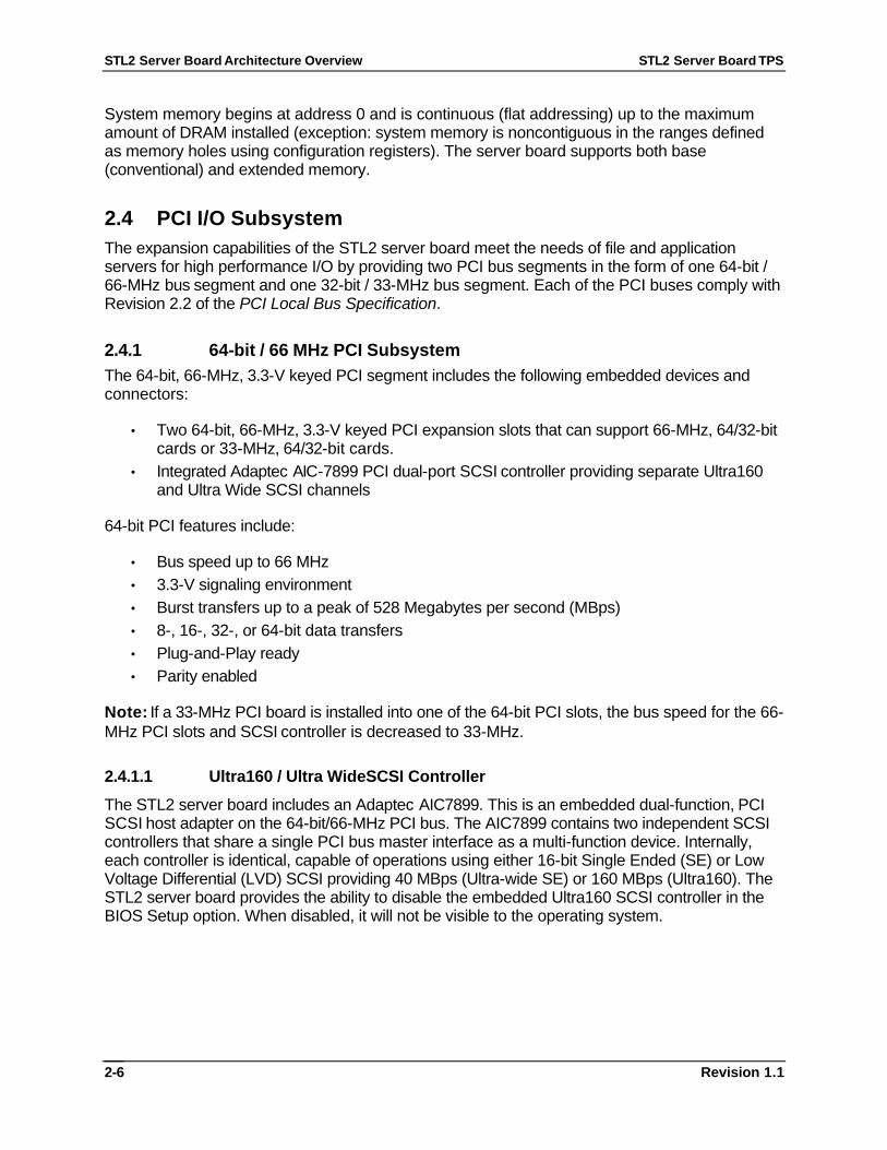
high-performance bus master interface can eliminate the intermediate copy step in RX/TX frame copies, resulting in faster frame processing.
The network operating system (OS) communicates with the 82559 using a memory-mapped I/O interface, PCI interrupt connected directly to the I/O Controller Hub (ICH), and two large receive and transmit FIFOs. The receive and transmit FIFOs prevent data overruns or underruns while waiting for access to the PCI bus, and also enable back-to-back frame transmission within the minimum 960ns inter-frame spacing. The figure below shows the PCI signals supported by the 82559:
i82559 NIC
PAR
STOP_L
TRDY_L
C/BE[3::0]_L
FRAME_L
AD[31::0]
SERR_L
PCI_CLK
RST_LPERR_L
GNT_L
IRDY_L
DEVSEL_LIDSELREQ_L
PCI_INT_L
Figure 2-1. Embedded NIC PCI Signals
2.4.2.1.1 Supported Network Features
The 82559 contains an IEEE MII compliant interface to the components necessary to implement an IEEE 802.3 100Base TX network connection. The STL2 supports the following features of the 82559 controller:
• Glueless 32-bit PCI Bus Master Interface (Direct Drive of Bus), compatible with PCI Bus Specification, revision 2.1 / 2.2
• Chained memory structure, with improved dynamic transmit chaining for enhanced performance
• Programmable transmit threshold for improved bus utilization • Early receive interrupt for concurrent processing of receive data • On-chip counters for network management • Autodetect and autoswitching for 10 or 100 Mbps network speeds • Support for both 10 Mbps and 100 Mbps networks, full or half duplex-capable, with back-
to-back transmit at 100 Mbps
STL2 Server Board Architecture Overview STL2 Server Board TPS
Revision 1.1 2-10
• Integrated physical interface to TX magnetics • The magnetics component terminates the 100Base-TX connector interface. A flash
device stores the network ID. • Support for Wake-on-LAN (WOL)
2.4.2.2 Video Controller
The STL2 server board includes an ATI Rage IIC video controller, 4-MB video SGRAM, and support circuitry for an embedded SVGA video subsystem. The Rage IIC, 64-bit VGA Graphics Accelerator contains a SVGA video controller, clock generator, BitBLT engine, and RAMDAC. Two 512 K x 32 SGRAM chips provide 4 MB of 10ns video memory.
The SVGA subsystem supports a variety of modes: up to 1280 X 1024 resolution, and up to 16.7 Million colors. It also supports analog VGA monitors, single- and multi-frequency, interlaced and non-interlaced, up to 100 Hz vertical refresh frequency. The STL2 server board provides a standard 15-pin VGA connector, and external video blanking logic for server management console redirection support.
2.4.2.2.1 Video Controller PCI Signals
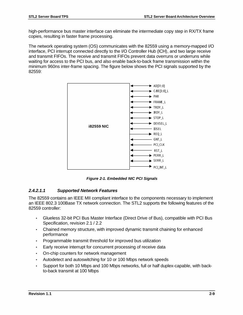
The Rage IIC supports a minimal set of 32-bit PCI signals because it never acts as a PCI master. As a PCI slave, the device requires no arbitration or interrupts.
Rage IIC
PAR
STOP_L
TRDY_L
C/BE[3::0]_L
FRAME_L
AD[31::0]
SERR_L
PCI_CLK
RST_LPERR_L
IRDY_L
DEVSEL_LIDSEL
PCI_INT_L
Figure 2-2. Video Controller PCI Signals

STL2 Server Board TPS STL2 Server Board Architecture Overview
Revision 1.1
2-11
2.4.2.2.2 Video Controller PCI Commands
The Rage IIC supports the following PCI commands:
Table 2-4. Video Controller Supported PCI Commands
Rage II C Support
C/BE[3::0]_L Command Type Target Master
0000 Interrupt Acknowledge No No
0001 Special Cycle No No
0010 I/O Read Yes No
0011 I/O Write Yes No
0100 Reserved No No
0101 Reserved No No
0110 Memory Read Yes No
0111 Memory Write Yes No
1000 Reserved No No
1001 Reserved No No
1010 Configuration Read Yes No
1011 Configuration Write Yes No
1100 Memory Read Multiple No No
1101 Dual Address Cycle No No
1110 Memory Read Line No No
1111 Memory Write and Invalidate No No
2.4.2.2.3 Video Modes
The Rage IIC supports all standard IBM* VGA modes. The following tables show the standard resolutions that this implementation supports, including the number of colors and the refresh rate.
Table 2-5. Standard VGA Modes
Resolution Refresh Rate (Hz) Colors
640x480 200 256
800x600 200 256
1024x768 150 256
1152x864 120 256
1280x1024 100 256
1600x1200 76 256
640x480 200 65K
800x600 200 65K
1024x768 150 65K
1152x864 120 65K
640x480 200 16.7 M
800x600 160 16.7 M
STL2 Server Board Architecture Overview STL2 Server Board TPS
Revision 1.1 2-12
2.4.2.3 IB6566 South Bridge
The IB6566 South Bridge is a PCI device that provides multiple PCI functions in a single package: PCI-to-ISA bridge, PCI IDE interface, PCI USB controller, and power management controller. Each function within the IB6566 South Bridge has its own set of configuration registers. Once configured, each appears to the system as a distinct hardware controller sharing the same PCI bus interface.
On the STL2 baseboard, the primary role of the IB6566 South Bridge is to provide the gateway to all PC-compatible I/O devices and features. The STL2 server board uses the following IB6566 South Bridge features:
• PCI interface • IDE interface • USB interface • PC-compatible timer/counters and Direct Memory Access (DMA) controllers • Baseboard Plug-and-Play support • General purpose I/O • Power management • APIC and 82C59 interrupt controller • Host interface for AT compatible signaling • Internal only ISA bus (no ISA expansion connectors) bridge for communication with Super
I/O, BIOS flash and BMC
The following sections describe each supported feature as used on the STL2 server board.
2.4.2.3.1 PCI Interface
The IB6566 South Bridge fully implements a 32-bit PCI master/slave interface, in accordance with Revision 2.2 of the PCI Local Bus Specification. On the STL2 server board, the PCI interface operates at 33 MHz, using the 5V-signaling environment.
2.4.2.3.2 PCI Bus Master IDE Interface
The IB6566 South Bridge acts as a PCI-based enhanced IDE 32-bit interface controller for intelligent disk drives that have disk controller electronics on-board. The server board includes a single IDE connector, featuring 40 pins (2 x 20) that support a master and a slave device. The IDE controller provides support for an internally mounted CD-ROM.
The IDE controller has the following features:
• Programmed Input/Output (PIO) and DMA transfer modes • Mode 4 timings • Transfer rates up to 33 MBps • Buffering for PCI/IDE burst transfers • Master/slave IDE mode • Support for up to two devices
STL2 Server Board TPS STL2 Server Board Architecture Overview
Revision 1.1
2-13
2.4.2.3.3 USB Interface
The IB6566 South Bridge contains a USB controller and USB hub. The USB controller moves data between main memory and the two USB connectors provided.
The STL2 server board provides a dual external USB connector interface. Both ports function identically and with the same bandwidth. The external connector is defined by Revision 1.0 of the USB Specification.
2.4.2.4 Compatibility Interrupt Control
The IB6566 South Bridge provides the functionality of two 82C59 Programmable Interrupt Controller (PIC) devices, for ISA-compatible interrupt handling.
2.4.2.5 APIC
The IB6566 South Bridge integrates a 16-entry I/O APIC that is used to distribute 16 PCI interrupts. It also includes an additional 16-entry I/O APIC for distribution of legacy ISA interrupts.
2.4.2.6 Power Management
One of the embedded functions of IB6566 South Bridge is a power management controller. The STL2 server board uses this to implement ACPI-compliant power management features. STL2 supports sleep states s0, s1, s4, and s5.
2.5 Chipset Support Components
2.5.1 Legacy I/O (Super I/O) National* PC97317VUL The National* PC97317VUL Super I/O Plug-and-Play Compatible with ACPI-Compliant Controller/Extender is used on the STL2 server board. This device provides the system with:
• Real-time Clock (RTC) • Two serial ports • One parallel port • Floppy disk controller (FDC) • PS/2-compatible keyboard and mouse controller • General purpose I/O pins • Plug-and-Play functions • A power management controller
The STL2 server board provides the connector interface for the floppy, dual serial ports, parallel port, PS/2 mouse and the PS/2 keyboard. Upon reset, the Super I/O (SIO) reads the values on strapping pins to determine the boot-up address configuration.
STL2 Server Board Architecture Overview STL2 Server Board TPS
Revision 1.1 2-14
2.5.1.1 Serial Ports
Two 9-pin connectors in D-Sub housing are provided for serial port A and serial port B. Both ports are compatible with 16550A and 16450 modes, and both are re-locatable. Each serial port can be set to one of four different COM-x ports, and each can be enabled separately. When enabled, each port can be programmed to generate edge- or level-sensitive interrupts. When disabled, serial port interrupts are available to add-in cards.
2.5.1.2 Parallel Port
The STL2 baseboard provides a 25-pin parallel port connector. The SIO provides an IEEE 1284-compliant 25-pin bi-directional parallel port. BIOS programming of the SIO registers enables the parallel port and determines the port address and interrupt. When disabled, the interrupt is available to add-in cards.
2.5.1.3 Floppy Port
The FDC in the SIO is functionally compatible with floppy disk controllers CMOS 765B and 82077AA. The baseboard provides the 24-MHz clock, termination resistors, and chip selects. All other FDC functions are integrated into the SIO, including analog data separator and 16-byte FIFO.
2.5.1.4 Keyboard and Mouse Connectors
The keyboard controller is functionally compatible with the 8042A. The keyboard and mouse connectors are PS/2-compatible.
2.5.1.5 Real-time Clock
The PC97317VUL contains an MC146818-compatible real-time clock with external battery backup. The device also contains 242 bytes of general purpose battery-backed CMOS RAM. The real-time clock provides system clock and calendar information stored in non-volatile memory.
2.5.1.6 Plug-and-Play Functions / ISA Data Transfers
The PC97317VUL contains all signals for ISA compatible interrupts and DMA channels. It also provides ISA control, data, and address signals to transfer data to/from the BMC and the BIOS flash device. This ISA subsystem transfers all SIO peripheral control data to the IB6566 South Bridge as well.
2.5.1.7 Power Management Controller
The PC97317VUL component contains functionality that allows various events to allow the power-on and power-off of the system. This can be from PCI Power Management Events, the BMC, or the front panel. This circuitry is powered from stand-by voltage, which is present anytime the system is plugged into the AC outlet.
STL2 Server Board TPS STL2 Server Board Architecture Overview
Revision 1.1
2-15
2.5.2 BIOS Flash The STL2 baseboard incorporates an Intel® 5V FlashFile™ 28F008SA Flash Memory component. The 28F008SA is a high-performance 8 Mbit memory that is organized as 1 MB of 8 bits each. There are 16 64-KB blocks.
The 8-bit flash memory provides 1024K x 8 of BIOS and nonvolatile storage space. The flash device is directly addressed as 8-bit ISA memory. For more information, see the 5 Volt FlashFile™ Memory (28F008SA x8) Datasheet.
2.5.3 External Device Connectors The external I/O connectors provide support for a PS/2 compatible mouse and keyboard, an SVGA monitor, two serial port connectors, a parallel port connector, a LAN port, and two USB connections.
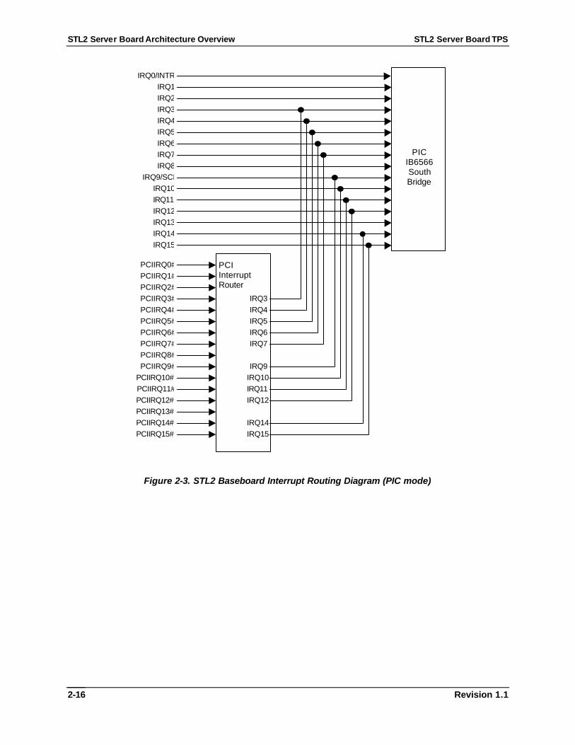
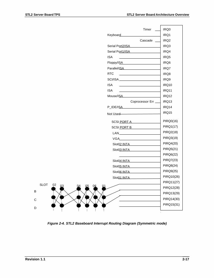
2.6 Interrupt Routing The STL2 server board interrupt architecture implements two I/O APICs and two PICs through the use of the integrated components in the IB6566 South Bridge component. The STL2 server board interrupt architecture allows first and second PCI interrupts to be mapped to compatible interrupt through the PCI Interrupt Address Index Register (I/O Address 0C00h) in the IB6566 South Bridge.
The IB6566 South Bridge uses integrated logic to map 16 PCI interrupts to EISA/ISA. In default or Extended APIC configurations, each PCI interrupt can be independently routed to one of the 11 EISA interrupts. The interrupt mapping logic for PCI interrupts is disabled when the make bit in the corresponding I/O APIC redirection table entry is disabled (clear). This interrupt routing mechanism allows a clean transition from PIC mode to an APIC during operating system boot.
2.6.1 Default I/O APIC The IB6566 South Bridge integrates a 16-entry I/O APIC which is used to distribute 16 PCI interrupts.
2.6.2 Extended I/O APIC An additional 16-entry I/O APIC is integrated in the IB6566 South Bridge to distribute EISA/ISA interrupts. This additional I/O APIC is enabled only when the IB6566 South Bridge is configured to the Extended APIC configuration.
STL2 Server Board Architecture Overview STL2 Server Board TPS
Revision 1.1 2-16
IRQ0/INTR
IRQ1
IRQ2
IRQ3
IRQ4
IRQ5
IRQ6
IRQ7
IRQ8
IRQ9/SCI
IRQ10
IRQ11
IRQ12
IRQ13
IRQ14
IRQ15
PCIIRQ0#
PCIIRQ1#
PCIIRQ2#
PCIIRQ3#
PCIIRQ4#
PCIIRQ5#
PCIIRQ6#
PCIIRQ7#
PICIB6566SouthBridge
PCIInterruptRouter
IRQ3
IRQ4
IRQ5
IRQ6
IRQ7
IRQ9
IRQ10
IRQ11
IRQ12
IRQ15
IRQ14
PCIIRQ8#
PCIIRQ9#
PCIIRQ10#
PCIIRQ11#
PCIIRQ12#
PCIIRQ13#
PCIIRQ14#
PCIIRQ15#
Figure 2-3. STL2 Baseboard Interrupt Routing Diagram (PIC mode)
STL2 Server Board TPS STL2 Server Board Architecture Overview
Revision 1.1
2-17
IRQ0
IRQ1
IRQ2
IRQ3
IRQ4
IRQ5
IRQ6
IRQ7
IRQ8
IRQ9
IRQ10
IRQ11
IRQ12
IRQ13
IRQ14
IRQ15
PIRQ0(16)
PIRQ1(17)
PIRQ2(18)
PIRQ3(19)
PIRQ4(20)
PIRQ5(21)
PIRQ6(22)
PIRQ7(23)
PIRQ8(24)
PIRQ9(25)
PIRQ10(26)
PIRQ11(27)
PIRQ12(28)
PIRQ13(29)
PIRQ14(30)
PIRQ15(31)
SCSI PORT A
SCSI PORT B
LAN
03
VGA
SLOT 04 0605
B
C
D
01
Timer
Cascade
Coprocessor Err
Keyboard
RTC
Serial Port2/ISA
Mouse/ISA
Serial Port1/ISA
Floppy/ISA
Parallel/ISA
P_IDE/ISA
ISA
SCI/ISA
ISA
ISA
Slot02 INTA
Slot03 INTA
Slot05 INTA
Slot04 INTA
Slot06 INTA
Slot01 INTA
Not Used
02
Figure 2-4. STL2 Baseboard Interrupt Routing Diagram (Symmetric mode)
STL2 Server Board Architecture Overview STL2 Server Board TPS
Revision 1.1 2-18
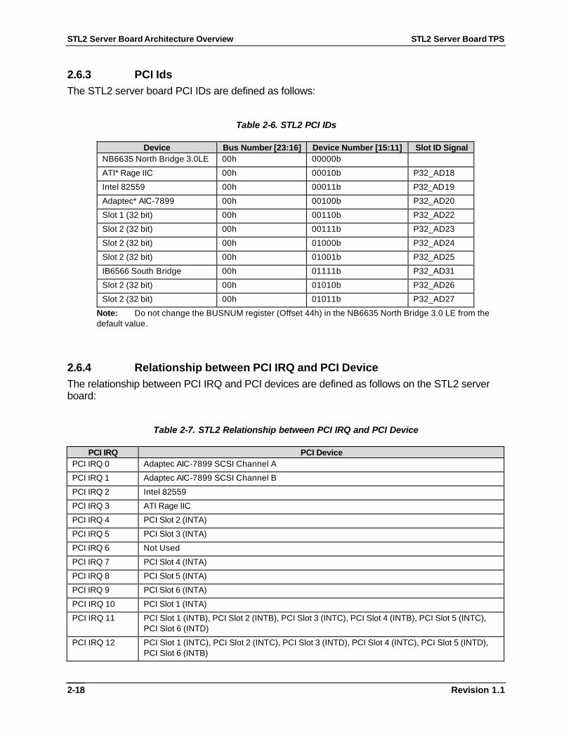
2.6.3 PCI Ids The STL2 server board PCI IDs are defined as follows:
Table 2-6. STL2 PCI IDs
Device Bus Number [23:16] Device Number [15:11] Slot ID Signal NB6635 North Bridge 3.0LE 00h 00000b
ATI* Rage IIC 00h 00010b P32_AD18
Intel 82559 00h 00011b P32_AD19
Adaptec* AIC-7899 00h 00100b P32_AD20
Slot 1 (32 bit) 00h 00110b P32_AD22
Slot 2 (32 bit) 00h 00111b P32_AD23
Slot 2 (32 bit) 00h 01000b P32_AD24
Slot 2 (32 bit) 00h 01001b P32_AD25
IB6566 South Bridge 00h 01111b P32_AD31
Slot 2 (32 bit) 00h 01010b P32_AD26
Slot 2 (32 bit) 00h 01011b P32_AD27
Note: Do not change the BUSNUM register (Offset 44h) in the NB6635 North Bridge 3.0 LE from the default value.
2.6.4 Relationship between PCI IRQ and PCI Device The relationship between PCI IRQ and PCI devices are defined as follows on the STL2 server board:
Table 2-7. STL2 Relationship between PCI IRQ and PCI Device
PCI IRQ PCI Device PCI IRQ 0 Adaptec AIC-7899 SCSI Channel A
PCI IRQ 1 Adaptec AIC-7899 SCSI Channel B
PCI IRQ 2 Intel 82559
PCI IRQ 3 ATI Rage IIC
PCI IRQ 4 PCI Slot 2 (INTA)
PCI IRQ 5 PCI Slot 3 (INTA)
PCI IRQ 6 Not Used
PCI IRQ 7 PCI Slot 4 (INTA)
PCI IRQ 8 PCI Slot 5 (INTA)
PCI IRQ 9 PCI Slot 6 (INTA)
PCI IRQ 10 PCI Slot 1 (INTA)
PCI IRQ 11 PCI Slot 1 (INTB), PCI Slot 2 (INTB), PCI Slot 3 (INTC), PCI Slot 4 (INTB), PCI Slot 5 (INTC), PCI Slot 6 (INTD)
PCI IRQ 12 PCI Slot 1 (INTC), PCI Slot 2 (INTC), PCI Slot 3 (INTD), PCI Slot 4 (INTC), PCI Slot 5 (INTD), PCI Slot 6 (INTB)
STL2 Server Board TPS STL2 Server Board Architecture Overview
Revision 1.1
2-19
PCI IRQ 13 PCI Slot 1 (INTD), PCI Slot 2 (INTD), PCI Slot 3 (INTB), PCI Slot 4 (INTC), PCI Slot 5 (INTD), PCI Slot 6 (INTB)
STL2 Server Board Architecture Overview STL2 Server Board TPS
2-20 Revision 1.1
< This page intentionally left blank >
STL2 Server Board TPS Server Management
Revision 1.1
3-21
3. Server Management
This section describes the features of the server management subsystem for the STL2 server board. The server management subsystem consists of the BIOS, hardware, and firmware features built into the server board. These features provide hardware monitoring, control, and logging to improve the reliability, availability, and serviceability of the server system.
The server management subsystem conforms to the IPMI (Intelligent Platform Management Interface) v1.0 specification. IPMI defines a standardized, abstracted, message-based interface between system management software and the platform management hardware.
The following comprise the major elements of the server management architecture for the STL2 server board.
• Baseboard Management Controller (BMC) • Sensors • Sensor Data Record (SDR) Repository and System Event Log (SEL) • Field Replaceable Unit (FRU) Information
3.1 Baseboard Management Controller The STL2 server management functionality is concentrated in the BMC. The BMC is comprised of a Dallas* Semiconductor DS80CH11 (or equivalent) microcontroller and associated circuitry located on the STL2 server board. The BMC and associated circuits are powered from a 5-V DC standby voltage, which remains active when system power is switched off, but the AC power source is still on and connected.
A major function of the BMC is to autonomously monitor system management events and log the occurrence in the nonvolatile System Event Log (SEL). The events being monitored include over/under temperature and over/under voltage conditions, fan failure, or chassis intrusion. To enable accurate monitoring, the BMC maintains the nonvolatile Sensor Data Record (SDR) from which sensor information can be retrieved. The BMC provides an ISA host interface to SDR sensor information, so that software running on the server can poll and retrieve the server’s current status. The BMC also provides the interface to the monitored information and SEL that System Management Software, such as Intel® Server Control, uses to poll and retrieve the platform status.
The BMC performs the following functions:
• Monitors server boad temperature and voltage • Monitors processor presence and controls Fault Resilient Boot (FRB) • Detects and indicates baseboard fan failure • Manages the SEL interface • Manages the SDR Repository interface • Monitors the SDR/SEL timestamp clock • Monitors the system management watchdog timer • Monitors the periodic SMI timer

Server Management STL2 Server Board TPS
Revision 1.1 3-22
• Monitors the event receiver • Controls secure mode, inlucluding video blanding, diskett write-protect monitoring, and
fornt panel lock/unlock initiation • Controls Wake-on-Lan via Magic Packet* support
3.2 Hardware Sensors The following table lists the hardware sensors present on the STL2 server board.
Table 3-1. STL2 Hardware Sensors
Sensor Number
Sensor Type Monitoring Device
01h Temperature ADM1024 Temperature
02h Processor 1 internal
03h Processor 2 internal
20h Voltage 3.3 V
21h 5 V
22h 12 V
23h 3.3 V Standby
24h Processor 1
25h Processor 2
29h 1.5 V
2Ah 2.5 V
2Ch SCSI-A 2.85 V
2Dh SCSI-B 2.85 V
2Eh SCSI-A Vref1
2Fh SCSI-A Vref2
30h SCSI-A Vref3
31h SCSI-B Vref1
32h SCSI-B Vref2
33h SCSI-B Vref3
34h Voltage (Discrete) Performance Lags
40h Fan Baseboard Fan 1
41h Baseboard Fan 2
42h Baseboard Fan 3
60h Processor Processor 1 State
61h Processor 2 State
70h Power Distribution Board Soft Power Control Failure (bit 5) Interlock Power
71h Power Distribution Board Supply 1 Power supply Failure detected (bit 1)
72h Power Distribution Board Supply 2 Power supply Failure detected (bit 1)
7Fh Power Redundancy Lost Redundancy Lost (bit 1) Redundancy Regained (bit 0)
90h Chassis Intrusion ID Drive Bay Intrusion (bit 1) LAN Leash Lost (bit 4)

STL2 Server Board TPS Server Management
Revision 1.1
3-23
Sensor Number
Sensor Type Monitoring Device
LAN Leash Lost (bit 4)
91h Security Violation Secure Mode Violation Attempt (bit 0)
92h Memory Error ECC multiple bit error (bit 1) ECC single bit error (bit 0)
93h POST Memory Resize
94h BIOS POST (Error) Code
95h Log Disable Log Area Reset / Cleared (bit 2) ECC single bit Error Disable (bit 0)
96h System Event Original Equipment Manufacturer (OEM) System Event (Hard Reset) (bit 1) System
97h Critical Interrupt PCI SERR (bit 5) PCI PERR (bit 4) Front Panel NMI (Dump SW) (bit 0)
98h Button Reset Button (bit 2) Sleep Button (bit 1) Power Button (bit 0)
99h No Processor or Termination Board
9Ah Boot Init User requested Preboot Execution Environment (PXE) boot (bit 3) Initiated by power up (bit 0)
9Bh Boot Error PXE Server not found (bit 2) No bootable media (bit 0)
9Ch OS Boot
9Dh OS Stop
9Fh ACPI State Sleeping in S1 state (bit 8) G3/Mechanical Off (bit 7) S5 / G2 Soft Off (bit 5) S4 (bit 4)
A0h BMC Watchdog BMC Watchdog Timer (WDT) Timeout
C0h Chassis Intrusion ID (Disable) Processor Area Intrusion (bit 4)
C1h Chassis Intrusion ID Drive Bay Intrusion (bit 1)
F3h Server Management Interrupt (SMI) State
SMI Stall State
The following table provides a list of System Event Log (SEL) events supported by the STL2 server board.
Table 3-2. STL2 Supported System Event Log (SEL) events
Sensor Type Sensor Type Code
Sensor-Specific Offset
Event Remarks
Reserved 00h – Reserved
Temperature 01h – Temperature An error occurred at thermal sensors
Server Management STL2 Server Board TPS
Revision 1.1 3-24
Sensor Type Sensor Type Code
Sensor-Specific Offset
Event Remarks
Voltage 02h – Voltage An error occurred at voltage sensors
01h Performance Lags In the single-end event mode, even if SCSI is available for a different mode event.
Fan 04h – Fan An error occurred at fan sensors.
Physical Security
05h 01h Drive Bay Intrusion Front cover has been opened or closed
03h Processor area intrusion Side (Chassis) cover has been opened or closed.
04h LAN Connection Lost
(System has been unplugged from LAN)
LAN cable has been plugged in or unplugged.
Platform Security Violation Attempt
06h 00h Secured Mode Violation Attempt
Power/sleep switch has been activated while in Secure Mode
03h Pre-boot Password Violation (network boot Password)
Bad Password at PXE Boot
Processor 07h 00h IERR Processor IERR has occurred
01h Thermal Trip Processor Thermal Trip has occurred
02h FRB1/BIST Failure BIST Error has occurred
04h FRB3/Processor Startup/Initialization failure (Processor didn’t start)
FRB3 Timeout has been detected
08h Processor disabled A processor has been disabled
Memory 0Ch 00h Correctable ECC ECC 1-bit error occurred
01h Uncorrectable ECC ECC 2-bit error occurred
POST Memory Resize
0Eh POST Memory Resize Displays the total amount of memory after memory failure
POST Error 0Fh POST Error POST Error occurred
Event Logging Disabled
10h 00h Correctable Memory Error Logging Disabled
Displays ECC single bit error monitoring disabled
01h Event ‘Type’ Logging Disabled Monitoring of a certain event type has been disabled
02h Log Area Reset/Cleared Displays the SEL area cleared.
03h All Event Logging Disabled Monitor for the entire BMC has been disabled.
System Event 12h 00h System Reconfigured Setup change has occurred
01h OEM System Boot Event (Hard Reset)
Cold reset has been issued

STL2 Server Board TPS Server Management
Revision 1.1
3-25
Sensor Type Sensor Type Code
Sensor-Specific Offset
Event Remarks
Critical Interrupt 13h 00h Front Panel Non-Maskable Interrupt (NMI) Dump Switch
Dump switch has been activated
02h I/O channel check NMI ISA I/O Check has occurred.
04h PCI SERR PCI SERR occurred
05h PCI PERR PCI PERR occurred
Button 14h 00h Power Button Power switch has been activated
01h Sleep Button Sleep switch has been activated
02h Reset Button Reset switch has been activated
Module / Board 15h Processor / Terminator Missing
Processor / Terminator is not mounted correctly
System Boot Initiated
1Dh 03h User requested PXE boot PXE (Network) Booted
04h Automatic boot to diagnostic When the maintenance Utility Booted
Boot Error 1Eh 00h No bootable media Boot Media does not exist.
02h PXE Server not found PXE Server is not found
00h C: boot completed ESM Pro installed OS has been booted
02h PXE boot completed PXE boot for the express server is finished (not supported)
03h Diagnostic boot completed Maintenance Utility has been booted (not supported)
04h CD-ROM boot completed The server has been booted (not supported)
OS Critical Stop 20h 00h Stop during OS load / Initialization
OS stalled during startup
01h Run-time Stop OS stalled during startup
System ACPI Power State
22h 00h S0 / G0 Working DC is ON
01h S1 “sleeping with system hardware and processor context Maintained”
S1 Sleep State
04h S4 “non-volatile sleep / suspend-to disk”
S4 Sleep State
05h S5 / G2 “soft-off” DC is OFF
07h G3 / Mechanical Off AC is OFF
08h Sleeping (cannot differentiate between S1-S3)
SUSC# OS has been asserted without the instruction to sleep
Watchdog 2 23h 01h Hard Reset POST/Boot monitor timed out
02h Power Down OS WDT shut down after the monitor timeout
Server Management STL2 Server Board TPS
Revision 1.1 3-26
Sensor Type Sensor Type Code
Sensor-Specific Offset
Event Remarks
08h Timer Interrupt OS WDT monitor timed out
SMI Timeout F3h SMI Timeout SMI# has been asserted for more than ten seconds
Emergency Management Port (EMP)
F5h 00h Communication Error Communication is unavailable even though the BMC is in communication status
Sensor Failure F6h 00h I2C Bus Device Address Not Acknowledged
SMBus Device does not answer.
01h I2C Bus Device Error Detected Other access errors
02h I2C Bus Timeout SMBus Timeout error
OEM Reserved F7h - FFh
3.3 ACPI The Advance Configuration and Power Interface (ACPI)-aware operating system can place the system into a state where the hard drives spin down, the sytem fans stop, and all processing is halted. In this state the power supply is still on and the processors still dissipate some power, such that the power supply fan and processor fans are still running.
Note: ACPI requires an operating system that supports this feature.
The ACPI sleep states discussed below are defined as:
• s0: Normal running state • s1: Processor sleep state. No content is lost in this state and the processor caches
maintain coherency. • s4: Hibernate or Save to Disk. The memory and machine state are saved to disk.
Pressing the power button or another wakeup event restores the system state from the disk and resumes normal operation. This assumes that no hardware changes were made to the system while it was off.
• s5: Soft off. Only the RTC section of the chip set and the BMC are running in this state.
The STL2 server board supports sleep states s0, s1, s4, and s5. When the server board is operating in ACPI mode, the OS retains control of the system and the OS policy determines the entry methods and wake up sources for each sleep state – sleep entry and wake up event capabilites are provided by the hardware but are enabled by the OS.
With future versions of Microsoft* Windows* 9X that support ACPI, the system BIOS supports only sleep states s0, s1, and s5. With future versions of Microsoft Windows NT* that support ACPI, the system BIOS will support sleep states s0, s1, s4, and s5.
3.4 AC Link Mode The AC link mode allows the system to monitor its AC input power so that if AC input power is lost and then restored, the system returns to one of the following preselected settings:
• Power On

STL2 Server Board TPS Server Management
Revision 1.1
3-27
• Last State (Factory Default Setting) • Stay Off
The AC link mode settings can be changed by running the BIOS Setup Utility.
3.5 Wake On LAN Function The remote power-on function turns on the system power by way of a network or modem. If the system power is set to Off, it can be turned on remotely by sending a specific packet from the main computer to the remote system.
Note: The standard default value of the remote power-on function is “Disabled”. The Wake-on-LAN / Ring function can changed by setting the option to “Enabled” in the BIOS Setup Utility.

STL2 Server Board Architecture Overview STL2 Server Board TPS
3-28 Revision 1.1
< This page intentionally left blank >
STL2 Server Board TPS Basic Input Output System (BIOS)
Revision 1.1
4-29
4. Basic Input Output System (BIOS)
This section describes BIOS embedded software for the STL2 board set. The BIOS contains standard PC-compatible basic input/output (I/O) services, standard Intel® server features, plus the STL2 system-specific hardware configuration routines and register default settings, embedded in Flash read-only memory (ROM). This section also describes BIOS support utilities (not ROM-resident) that are required for system configuration and flash ROM update.
The BIOS is implemented as firmware that resides in the flash ROM. Support for applicable baseboard peripheral devices (SCSI, NIC, and video adapters), which is also loaded into the baseboard flash ROM, is not specified in this document. Hooks are provided to support adding BIOS code for these adapters; the binaries must be obtained from the peripheral device manufacturers and loaded into the appropriate locations.
4.1 BIOS Overview The term BIOS, as used in the context of this section, refers to the system BIOS, the BIOS Setup and option ROMs for on-board peripheral devices that are contained in the system flash. System BIOS controls basic system functionality using stored configuration values. The terms flash ROM, system flash, and BIOS flash may be used interchangeably in this section.
The term BIOS Setup refers to the flash ROM-resident setup utility that provides the user with control of configuration values stored in battery-backed CMOS configuration RAM. The System Setup Utility (SSU), which also provides this functionality, is discussed in a separate document. BIOS Setup is closely tied with the system BIOS and is considered a part of BIOS.
Phoenix Phlash* (PHLASH.EXE) is used to load predefined areas of flash ROM with Setup, BIOS, and other code/data.
The following is the break-down of the STL2 product ID string:
• 4-byte board ID, ‘STL2’ • 1-byte board revision, starting from ‘0’ • 3-byte OEM ID, ‘86B’ for standard BIOS • 4-byte build number • 1-3 byte describing build type (D for development, A for Alpha, B for Beta, Pxx for
production version xx) • 6-byte build date in yymmdd format • 4-bytes time in hhmm format

Basic Input Output System (BIOS) STL2 Server Board TPS
Revision 1.1 4-30
4.1.1 System BIOS The system BIOS is the core of the flash ROM-resident portion of the BIOS. The system BIOS provides standard PC-BIOS services and support for some new industry standards, such as the Advanced Configuration and Power Interface Specification, Revision 1.0 and Wired For Management Baseline Specification, Revision 2.0. In addition, the system BIOS supports certain features that are common across all the Intel servers. These include:
• Security • Intel Multi-Processor Specification (MPS) support • Server management and error handling • CMOS configuration RAM management • OEM customization • PCI and Plug and Play (PnP) BIOS interface • Console redirection • Resource allocation support
BIOS setup is embedded in flash ROM and provides the means to configure on-board hardware devices and add-in cards. For more information, refer to Section 4.2, Setup Utility.
4.1.2 Flash Update Utility The system BIOS and the setup utility are resident in partitioned flash ROM. The device is in-circuit reprogrammable. On the STL2 platform, 1 MB of flash ROM is provided. The STL2 BIOS does not support a SecureBIOS feature like some server products from Intel. This is because the addition of SecureBIOS increases boot time, and complexities, and does not provide compelling benefits for the STL2 platform.
The Phoenix Phlash Utility may be used to reprogram the BIOS operational code located in the flash ROM. A BIOS image is provided on a diskette in the form of a binary file that is read by the Phoenix Phlash Utility. Baseboard revisions may create hardware incompatibilities and may require different BIOS code.
4.1.2.1 System Flash ROM Layout
The flash ROM contains system initialization routines, BIOS strings, BIOS Setup, and run-time support routines. The exact layout is subject to change, as determined by Intel. A 16-KB user block is available for user ROM code and another 128-KB block is available for custom logos. The flash ROM also contains compressed initialization code for on-board peripherals such as SCSI, NIC, and video controllers. The BIOS image contains all the BIOS components at appropriate locations. The Phoenix Phlash Utility can be used to reprogram the BIOS operational code areas.
At run time, none of the flash blocks is visible at the aliased addresses below 1 MB due to shadowing. Intel reserves the right to change the flash map without notice.
A 64-KB parameter block in the flash ROM is dedicated to storing configuration data that controls extended system configuration data (ESCD), on-board SCSI configuration, OEM configuration areas, etc. The block is partitioned into separate areas for logically different data. Application

STL2 Server Board TPS Basic Input Output System (BIOS)
Revision 1.1
4-31
software must use standard advanced programmable interrupts (APIs) to access these areas and may not access the data directly.
4.2 Setup Utility This section describes the ROM resident setup utility that provides the means to configure the platform. The setup utility is part of the system BIOS and allows limited control over on-board resources such as the parallel port and mouse. The following topics are covered below:
• Setup utility operation • Configuration CMOS RAM definition • Function of the CMOS clear jumper
4.2.1 Configuration Utilities Overview Configuration of on-board devices is done using the setup utility that is embedded in flash ROM. Setup provides sufficient configuration functionality to boot a system diskette or CD-ROM. The System Setup Utility (SSU), which is discussed in a separate document, is released on diskette or CD-ROM. Setup is always provided in flash for basic system configuration.
The configuration utilities modify CMOS RAM and Non-Volatile Random Access Memory (NVRAM) under direction of the user. The BIOS POST routines and the BIOS Plug-N-Play Auto-configuration Manager accomplish the actual hardware configuration. The configuration utilities always update a checksum for both areas, so that any potential data corruption is detectable by the BIOS before the hardware configuration takes place. If data is corrupted, the BIOS requests that the user reconfigure the system and reboot.
4.2.2 Setup Utility Operation The ROM-resident setup utility configures only on-board devices. The setup utility screen is divided into four functional areas. Table 4-1 describes each area:
Table 4-1. Setup Utility Screen
Functional Area Description
Keyboard Command Bar Located at the bottom of the screen. This bar displays the keyboard commands supported by the setup utility.
Menu Selection Bar Located at the top of the screen. Displays the various major menu selections available to the user. The server setup utility major menus are: Main Menu, Advanced Menu, Security Menu, System Menu, Boot Menu, and the Exit Menu.
Options Menu Each Option Menu occupies the left and center sections of the screen. Each menu contains a set of features. Selecting certain features within a major Option Menu drops you into submenus.
Item Specific Help Screen Located at the right side of the screen is an item-specific Help screen.

Basic Input Output System (BIOS) STL2 Server Board TPS
Revision 1.1 4-32
4.2.2.1 Entering Setup Utility
During POST operation, the user is prompted to enter Setup using the F2 function key as follows:
Press <F2> to enter Setup
After the F2 key is pressed, a few seconds might pass before Setup is entered while POST finishes test and initialization functions that must be completed before Setup can be entered. When Setup is entered, the Main Menu options page is displayed.
4.2.2.2 Keyboard Command Bar
The bottom portion of the screen provides a list of commands that are used for navigating the Setup utility. These commands are displayed at all times, for every menu and submenu.
Each Setup menu page contains a number of features. Except those used for informative purposes, each feature is associated with a value field. This field contains user-selectable parameters. Depending on the security option chosen and in effect via password, a menu feature’s value can be changeable or not. If a value is cannot be changed due to insufficient security privileges or other reasons, the feature’s value field is inaccessible. The Keyboard Command Bar supports the following:
F1 Help Pressing F1 on any menu invokes the general Help window. This window describes the Setup key legend. The up arrow, down arrow, Page Up, Page Down, Home, and End keys scroll the text in this window.
Enter Execute Command The Enter key is used to activate submenus when the selected feature is a submenu, or to display a pick list if a selected feature has a value field, or to select a subfield for multi-valued features like time and date. If a pick list is displayed, the Enter key will undo the pick list, and allow another selection in the parent menu.
ESC Exit The ESC key provides a mechanism for backing out of any field. This key will undo the pressing of the Enter key. When the ESC key is pressed while editing any field or selecting features of a menu, the parent menu is re-entered. When the ESC key is pressed in any submenu, the parent menu is re-entered. When the ESC key is pressed in any major menu, the exit confirmation window is displayed and the user is asked whether changes can be discarded.
↑↑ Select Item The up arrow is used to select the previous value in a pick list, or the previous feature in a menu item’s option list. The selected item must then be activated by pressing the Enter key.
↓↓ Select Item The down arrow is used to select the next value in a menu item’s option list, or a value field’s pick list. The selected item must then be activated by pressing the Enter key.
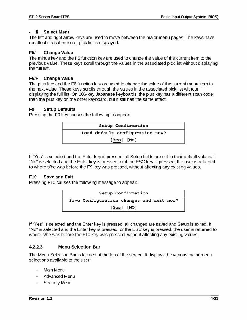
STL2 Server Board TPS Basic Input Output System (BIOS)
Revision 1.1
4-33
←← →→ Select Menu The left and right arrow keys are used to move between the major menu pages. The keys have no affect if a submenu or pick list is displayed.
F5/– Change Value The minus key and the F5 function key are used to change the value of the current item to the previous value. These keys scroll through the values in the associated pick list without displaying the full list.
F6/+ Change Value The plus key and the F6 function key are used to change the value of the current menu item to the next value. These keys scrolls through the values in the associated pick list without displaying the full list. On 106-key Japanese keyboards, the plus key has a different scan code than the plus key on the other keyboard, but it still has the same effect.
F9 Setup Defaults Pressing the F9 key causes the following to appear:
Setup Confirmation
Load default configuration now?
[Yes] [No]
If “Yes” is selected and the Enter key is pressed, all Setup fields are set to their default values. If “No” is selected and the Enter key is pressed, or if the ESC key is pressed, the user is returned to where s/he was before the F9 key was pressed, without affecting any existing values.
F10 Save and Exit Pressing F10 causes the following message to appear:
Setup Confirmation
Save Configuration changes and exit now?
[Yes] [NO]
If “Yes” is selected and the Enter key is pressed, all changes are saved and Setup is exited. If “No” is selected and the Enter key is pressed, or the ESC key is pressed, the user is returned to where s/he was before the F10 key was pressed, without affecting any existing values.
4.2.2.3 Menu Selection Bar
The Menu Selection Bar is located at the top of the screen. It displays the various major menu selections available to the user:
• Main Menu • Advanced Menu • Security Menu
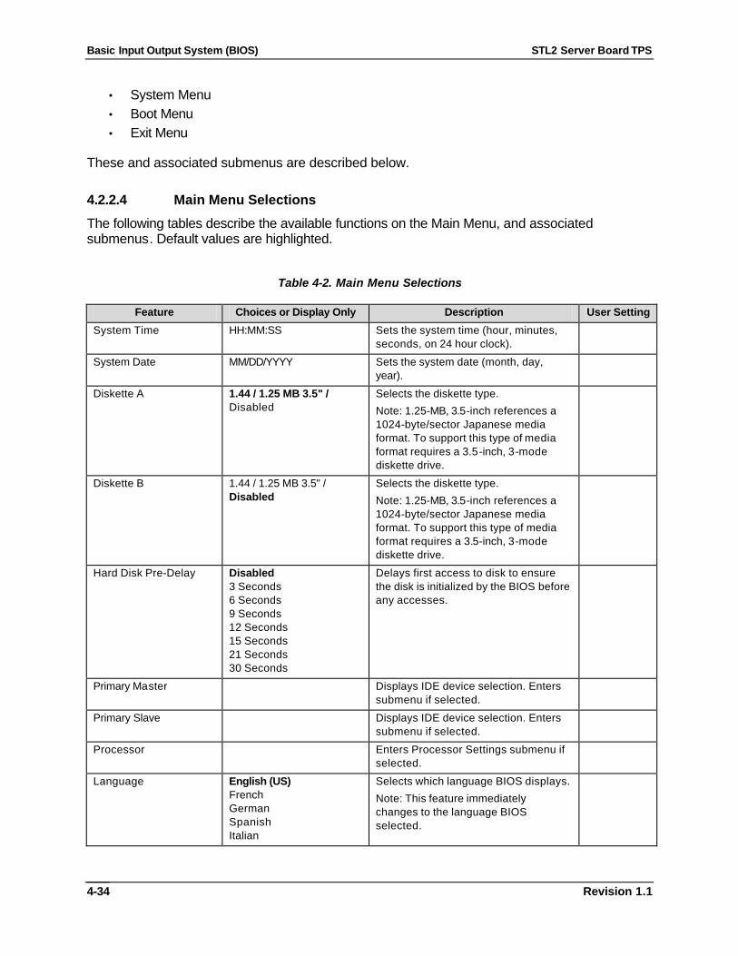
Basic Input Output System (BIOS) STL2 Server Board TPS
Revision 1.1 4-34
• System Menu • Boot Menu • Exit Menu
These and associated submenus are described below.
4.2.2.4 Main Menu Selections
The following tables describe the available functions on the Main Menu, and associated submenus. Default values are highlighted.
Table 4-2. Main Menu Selections
Feature Choices or Display Only Description User Setting
System Time HH:MM:SS Sets the system time (hour, minutes, seconds, on 24 hour clock).
System Date MM/DD/YYYY Sets the system date (month, day, year).
Diskette A 1.44 / 1.25 MB 3.5" / Disabled
Selects the diskette type.
Note: 1.25-MB, 3.5-inch references a 1024-byte/sector Japanese media format. To support this type of media format requires a 3.5-inch, 3-mode diskette drive.
Diskette B 1.44 / 1.25 MB 3.5" / Disabled
Selects the diskette type.
Note: 1.25-MB, 3.5-inch references a 1024-byte/sector Japanese media format. To support this type of media format requires a 3.5-inch, 3-mode diskette drive.
Hard Disk Pre-Delay Disabled 3 Seconds 6 Seconds 9 Seconds 12 Seconds 15 Seconds 21 Seconds 30 Seconds
Delays first access to disk to ensure the disk is initialized by the BIOS before any accesses.
Primary Master Displays IDE device selection. Enters submenu if selected.
Primary Slave Displays IDE device selection. Enters submenu if selected.
Processor Enters Processor Settings submenu if selected.
Language English (US) French German Spanish Italian
Selects which language BIOS displays.
Note: This feature immediately changes to the language BIOS selected.

STL2 Server Board TPS Basic Input Output System (BIOS)
Revision 1.1
4-35
Table 4-3. Primary Master and Slave Adapters Submenu Selections
Feature
Choices or Display Only Description
User Setting
Type Auto None CD-ROM ATAPI Removable IDE Removable Other ATAPI User
Select the type of device that is attached to the IDE channel
If User is selected, the user will need to enter the parameters of the IDE device (cylinders, heads and sectors).
Mult-Sector Transfers Disable 2 Sectors 4 Sectors 8 Sectors 16 Sectors
Specifies the number of sectors that are transferred per block during multiple sector transfers.
LBA Mode Control Disabled Enabled
Enable/Disable Logical Block Addressing instead of cylinder, head, sector addressing.
32 Bit I/O Disabled Enabled
Enable/Disable 32-Bit IDE data transfers
Transfer Mode Standard Fast PIO 1 Fast PIO 2 Fast PIO 3 Fast PIO 4 FPIO 3/ DMA 1 FPIO 4 / DMA 2
Select the method of moving data to and from the hard drive. (If Type: Auto is select, optimum transfer mode will be selected)
Ultra DMA Mode Disabled Enabled
Enable/Disable Ultra DMA mode (If Type: Auto is select, optimum transfer mode will be selected)
Table 4-4. Processor Settings Submenu Selections
Feature
Choices or Display Only Description
User Setting
Processor Speed XXX (Display Only). Indicates the processor speed.
Processor 1 Type XXX (Display Only). Indicates the CPUID of the installed processor.
Cache Ram XXXKB (Display Only). Indicates the cache RAM size.
Processor 2 Type XXX (Display Only). Indicates the CPUID of the installed processor.
Cache Ram XXXKB (Display Only). Indicates the cache RAM size.
Processor #1 Status Normal1 (Display Only)
Processor #2 Status Normal1 (Display Only)
Clear Processor Errors Press Enter Clears the processor error information.
Processor Error Pause Enabled Disabled
If enabled, the POST operation pauses if a processor error occurs.
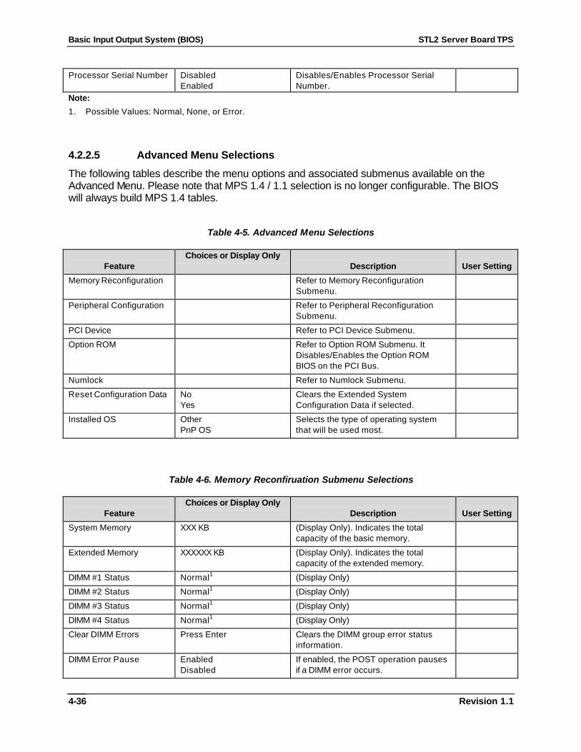
Basic Input Output System (BIOS) STL2 Server Board TPS
Revision 1.1 4-36
Processor Serial Number Disabled Enabled
Disables/Enables Processor Serial Number.
Note:
1. Possible Values: Normal, None, or Error.
4.2.2.5 Advanced Menu Selections
The following tables describe the menu options and associated submenus available on the Advanced Menu. Please note that MPS 1.4 / 1.1 selection is no longer configurable. The BIOS will always build MPS 1.4 tables.
Table 4-5. Advanced Menu Selections
Feature
Choices or Display Only Description
User Setting
Memory Reconfiguration Refer to Memory Reconfiguration Submenu.
Peripheral Configuration Refer to Peripheral Reconfiguration Submenu.
PCI Device Refer to PCI Device Submenu.
Option ROM Refer to Option ROM Submenu. It Disables/Enables the Option ROM BIOS on the PCI Bus.
Numlock Refer to Numlock Submenu.
Reset Configuration Data No Yes
Clears the Extended System Configuration Data if selected.
Installed OS Other PnP OS
Selects the type of operating system that will be used most.
Table 4-6. Memory Reconfiruation Submenu Selections
Feature
Choices or Display Only Description
User Setting
System Memory XXX KB (Display Only). Indicates the total capacity of the basic memory.
Extended Memory XXXXXX KB (Display Only). Indicates the total capacity of the extended memory.
DIMM #1 Status Normal1 (Display Only)
DIMM #2 Status Normal1 (Display Only)
DIMM #3 Status Normal1 (Display Only)
DIMM #4 Status Normal1 (Display Only)
Clear DIMM Errors Press Enter Clears the DIMM group error status information.
DIMM Error Pause Enabled Disabled
If enabled, the POST operation pauses if a DIMM error occurs.
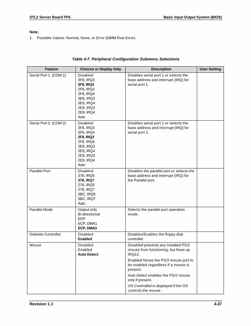
STL2 Server Board TPS Basic Input Output System (BIOS)
Revision 1.1
4-37
Note:
1. Possible Values: Normal, None, or Error (DIMM Row Error).
Table 4-7. Peripheral Configuration Submenu Selections
Feature Choices or Display Only Description User Setting
Serial Port 1: (COM 1) Disabled 3F8, IRQ3 3F8, IRQ4 2F8, IRQ3 2F8, IRQ4 3E8, IRQ3 3E8, IRQ4 2E8, IRQ3 2E8, IRQ4 Auto
Disables serial port 1 or selects the base address and interrupt (IRQ) for serial port 1.
Serial Port 2: (COM 2) Disabled 3F8, IRQ3 3F8, IRQ4 2F8, IRQ3 2F8, IRQ4 3E8, IRQ3 3E8, IRQ4 2E8, IRQ3 2E8, IRQ4 Auto
Disables serial port 2 or selects the base address and interrupt (IRQ) for serial port 2.
Parallel Port Disabled 378, IRQ5 378, IRQ7 278, IRQ5 278, IRQ7 3BC, IRQ5 3BC, IRQ7 Auto
Disables the parallel port or selects the base address and interrupt (IRQ) for the Parallel port.
Parallel Mode Output only Bi-directional EPP ECP, DMA1 ECP, DMA3
Selects the parallel port operation mode.
Diskette Controller Disabled Enabled
Disables/Enables the floppy disk controller.
Mouse Disabled Enabled Auto Detect
Disabled prevents any installed PS/2 mouse from functioning, but frees up IRQ12.
Enabled forces the PS/2 mouse port to be enabled regardless if a mouse is present.
Auto Detect enables the PS/2 mouse only if present.
OS Controlled is displayed if the OS controls the mouse.

Basic Input Output System (BIOS) STL2 Server Board TPS
Revision 1.1 4-38
Feature Choices or Display Only Description User Setting
SCSI Controller Disabled Enabled
Disables/Enables on-board SCSI controller. Frees resources.
LAN Controller Disabled Enabled
Disables/Enables on-board LAN controller. Frees resources.
VGA Controller Enabled Disabled
Disables/Enables on-board Video controller. Frees resources.
USB Controller Disabled Enabled
Enables/Disables on-board USB controller. Frees resources.
Table 4-8. PCI Device Submenu Selections
Feature Choices or Display Only Description User Setting
PCI IRQ1 through PCI IRQ14
Disabled Auto Select IRQ3 IRQ4 IRQ5 IRQ6 IRQ7 IRQ9 IRQ10 IRQ11 IRQ12
Specify which PIC IRQ a certain PCI IRQ maps to.
Table 4-9. Option ROM Submenu Selections
Feature Choices or Display Only Description User Setting
Onboard SCSI Enabled Disabled
Disables/Enables option ROM expansion for the on-board SCSI option ROM. This must be enable if a boot device is connected to the on-board device.
Onboard LAN Enabled Disabled
Disables/Enables option ROM expansion for the on-board LAN option ROM.
PCI Slot 1 Enabled Disabled
Disables/Enables the expansion of the option ROM for devices in PCI slot 1
PCI Slot 2 Enabled Disabled
Disables/Enables the expansion of the option ROM for devices in PCI slot 2
PCI Slot 3 Enabled Disabled
Disables/Enables the expansion of the option ROM for devices in PCI slot 3
PCI Slot 4 Enabled Disabled
Disables/Enables the expansion of the option ROM for devices in PCI slot 4
PCI Slot 5 Enabled Disabled
Disables/Enables the expansion of the option ROM for devices in PCI slot 5
PCI Slot 6 Enabled Disabled
Disables/Enables the expansion of the option ROM for devices in PCI slot 6
PCI Slot 7 Enabled Disabled
Disables/Enables the expansion of the option ROM for devices in PCI slot 7

STL2 Server Board TPS Basic Input Output System (BIOS)
Revision 1.1
4-39
Table 4-10. Numlock Submenu Selections
Feature Choices or Display Only Description User Setting
Numlock Auto On Off
Selects the power-on state for Numlock.
Key Click Disabled Enabled
Disables or enables keyclick.
Keyboard Auto-repeat Rate
2/sec 6/sec 10/sec 13.3/sec 18.5/sec 21.8/sec 26.7/sec 30/sec
Selects key repeat rate.
Keyboard Auto-repeat Delay
0.25 sec 0.5 sec 0.75 sec 1 sec
Selects delay before key repeat.
4.2.2.6 Security Menu Selections
Table 4-11. Security Menu Selections
Feature Choices or Display Only Description User Setting
Supervisor Password is Clear (Display only). Once set, this can be disabled by setting it to a null string, or by clearing password jumper on system board.
User Password is Clear (Display only). Once set, this can be disabled by setting it to a null string, or by clearing password jumper on system board
Set Supervisor Password Press Enter Supervisor password controls access to the setup utility.
When the <Enter> key is pressed, the user is prompted for a password; press ESC key to abort. Once set, this can be disabled by setting it to a null string, or by clearing password jumper on system board.
Set User Password Press Enter When the <Enter> key is pressed, the user is prompted for a password; press ESC key to abort. Once set, this can be disabled by setting it to a null string, or by clearing password jumper on system board.
Password on Boot Disabled Enabled
Disables or enables password entry on boot.
Fixed Disk Boot Sector Normal Write Protect
Write protects boot sector on hard disk.
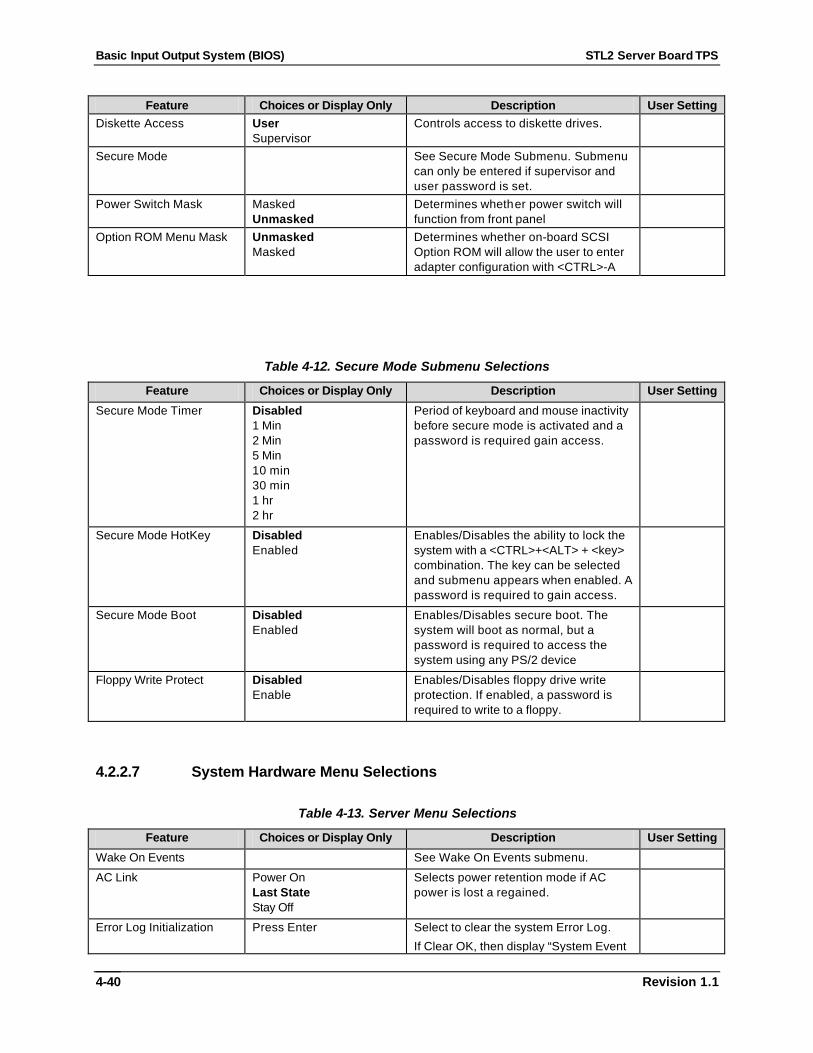
Basic Input Output System (BIOS) STL2 Server Board TPS
Revision 1.1 4-40
Feature Choices or Display Only Description User Setting
Diskette Access User Supervisor
Controls access to diskette drives.
Secure Mode See Secure Mode Submenu. Submenu can only be entered if supervisor and user password is set.
Power Switch Mask Masked Unmasked
Determines whether power switch will function from front panel
Option ROM Menu Mask Unmasked Masked
Determines whether on-board SCSI Option ROM will allow the user to enter adapter configuration with <CTRL>-A
Table 4-12. Secure Mode Submenu Selections
Feature Choices or Display Only Description User Setting
Secure Mode Timer Disabled 1 Min 2 Min 5 Min 10 min 30 min 1 hr 2 hr
Period of keyboard and mouse inactivity before secure mode is activated and a password is required gain access.
Secure Mode HotKey Disabled Enabled
Enables/Disables the ability to lock the system with a <CTRL>+<ALT> + <key> combination. The key can be selected and submenu appears when enabled. A password is required to gain access.
Secure Mode Boot Disabled Enabled
Enables/Disables secure boot. The system will boot as normal, but a password is required to access the system using any PS/2 device
Floppy Write Protect Disabled Enable
Enables/Disables floppy drive write protection. If enabled, a password is required to write to a floppy.
4.2.2.7 System Hardware Menu Selections
Table 4-13. Server Menu Selections
Feature Choices or Display Only Description User Setting
Wake On Events See Wake On Events submenu.
AC Link Power On Last State Stay Off
Selects power retention mode if AC power is lost a regained.
Error Log Initialization Press Enter Select to clear the system Error Log.
If Clear OK, then display “System Event
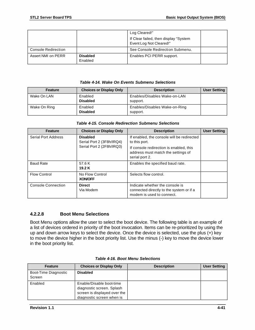
STL2 Server Board TPS Basic Input Output System (BIOS)
Revision 1.1
4-41
Log Cleared!”
If Clear failed, then display “System Event Log Not Cleared!”
Console Redirection See Console Redirection Submenu.
Assert NMI on PERR Disabled Enabled
Enables PCI PERR support.
Table 4-14. Wake On Events Submenu Selections
Feature Choices or Display Only Description User Setting
Wake On LAN Enabled Disabled
Enables/Disables Wake-on-LAN support.
Wake On Ring Enabled Disabled
Enables/Disables Wake-on-Ring support.
Table 4-15. Console Redirection Submenu Selections
Feature Choices or Display Only Description User Setting
Serial Port Address Disabled Serial Port 2 (3F8h/IRQ4) Serial Port 2 (2F8h/IRQ3)
If enabled, the console will be redirected to this port.
If console redirection is enabled, this address must match the settings of serial port 2.
Baud Rate 57.6 K 19.2 K
Enables the specified baud rate.
Flow Control No Flow Control XON/OFF
Selects flow control.
Console Connection Direct Via Modem
Indicate whether the console is connected directly to the system or if a modem is used to connect.
4.2.2.8 Boot Menu Selections
Boot Menu options allow the user to select the boot device. The following table is an example of a list of devices ordered in priority of the boot invocation. Items can be re-prioritized by using the up and down arrow keys to select the device. Once the device is selected, use the plus (+) key to move the device higher in the boot priority list. Use the minus (-) key to move the device lower in the boot priority list.
Table 4-16. Boot Menu Selections
Feature Choices or Display Only Description User Setting
Boot-Time Diagnostic Screen
Disabled
Enabled Enable/Disable boot-time diagnostic screen. Splash screen is displayed over the diagnostic screen when is
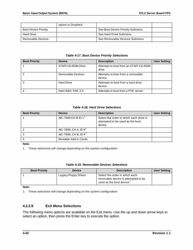
Basic Input Output System (BIOS) STL2 Server Board TPS
Revision 1.1 4-42
option is Disabled.
Boot Device Priority See Boot Device Priority Submenu
Hard Drive See Hard Drive Submenu
Removable Devices See Removable Devices Submenu
Table 4-17. Boot Device Priority Selections
Boot Priority Device Description User Setting
1 ATAPI CD-ROM Drive Attempts to boot from an ATAPI CD-ROM drive.
2 Removable Devices Attempts to boot from a removable device.
3 Hard Drive Attempts to boot from a hard drive device.
4 Intel UNDI, PXE-2.0 Attempts to boot from a PXE server.
Table 4-18. Hard Drive Selections
Boot Priority Device Description User Setting
1 AIC-7899,CH B ID 11 Select the order in which each drive is attempted to be used as the boot device.
2 AIC-7899, CH A, ID 91
3 AIC-7899, CH B, ID 41
4 Bootable Add-in Cards
Note:
1. These selections will change depending on the system configuration
Table 4-19. Removable Devices Selections
Boot Priority Device Description User Setting
1 Legacy Floppy Drives Select the order in which each removable device is attempted to be used as the boot device.1
Note:
1. These selections will change depending on the system configuration
4.2.2.9 Exit Menu Selections
The following menu options are available on the Exit menu. Use the up and down arrow keys to select an option, then press the Enter key to execute the option.
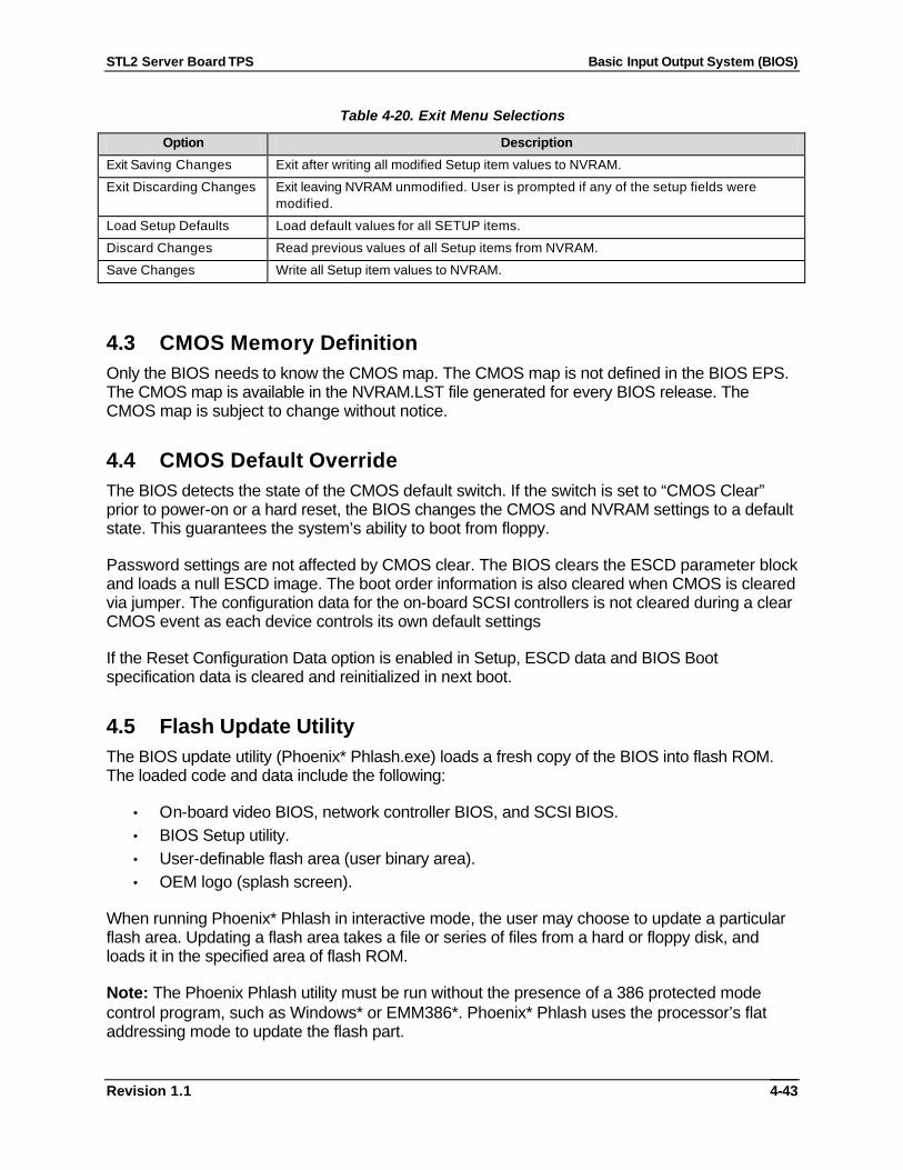
STL2 Server Board TPS Basic Input Output System (BIOS)
Revision 1.1
4-43
Table 4-20. Exit Menu Selections
Option Description
Exit Saving Changes Exit after writing all modified Setup item values to NVRAM.
Exit Discarding Changes Exit leaving NVRAM unmodified. User is prompted if any of the setup fields were modified.
Load Setup Defaults Load default values for all SETUP items.
Discard Changes Read previous values of all Setup items from NVRAM.
Save Changes Write all Setup item values to NVRAM.
4.3 CMOS Memory Definition Only the BIOS needs to know the CMOS map. The CMOS map is not defined in the BIOS EPS. The CMOS map is available in the NVRAM.LST file generated for every BIOS release. The CMOS map is subject to change without notice.
4.4 CMOS Default Override The BIOS detects the state of the CMOS default switch. If the switch is set to “CMOS Clear” prior to power-on or a hard reset, the BIOS changes the CMOS and NVRAM settings to a default state. This guarantees the system’s ability to boot from floppy.
Password settings are not affected by CMOS clear. The BIOS clears the ESCD parameter block and loads a null ESCD image. The boot order information is also cleared when CMOS is cleared via jumper. The configuration data for the on-board SCSI controllers is not cleared during a clear CMOS event as each device controls its own default settings
If the Reset Configuration Data option is enabled in Setup, ESCD data and BIOS Boot specification data is cleared and reinitialized in next boot.
4.5 Flash Update Utility The BIOS update utility (Phoenix* Phlash.exe) loads a fresh copy of the BIOS into flash ROM. The loaded code and data include the following:
• On-board video BIOS, network controller BIOS, and SCSI BIOS. • BIOS Setup utility. • User-definable flash area (user binary area). • OEM logo (splash screen).
When running Phoenix* Phlash in interactive mode, the user may choose to update a particular flash area. Updating a flash area takes a file or series of files from a hard or floppy disk, and loads it in the specified area of flash ROM.
Note: The Phoenix Phlash utility must be run without the presence of a 386 protected mode control program, such as Windows* or EMM386*. Phoenix* Phlash uses the processor’s flat addressing mode to update the flash part.

Basic Input Output System (BIOS) STL2 Server Board TPS
Revision 1.1 4-44
4.5.1 Loading the System BIOS The BIOS update utility (PHLASH) loads a new copy of the BIOS into Flash ROM. The loaded code and data include the following:
• On-board Video BIOS and SCSI BIOS • BIOS Setup Utility • Quiet Boot Logo Area
When running PHLASH in interactive mode, the user may choose to update a particular Flash area. Updating a flash area loads a file or a series of files from a hard or floppy disk into the specified area of Flash ROM.
To manually load a portion of the BIOS, the user must specify which data file(s) to load. The choices include
• PLATCBLU.BIN • PLATCXLU.BIN • PLATCXXX.BIN • PLATCXLX.BIN • PLATCXXU.BIN
The last three letters specify the functions to perform during the flash process:
• C = Rewrite BIOS • B = Rewrite Bootblock • L = Clear LOGO area • U = Clear user binary • X = place hold
This file is loaded into the PHLASH program with the /b=<bin file>.
The disk created by the BIOS.EXE program will automatically run phlash /s /b=PLATCXLU.BIN command in non-interactive mode. For a complete list of phlash switches, run phlash /h.
Once an update of the system BIOS is complete, the user is prompted for a reboot. The user binary area is also updated during a system BIOS update. User binary can be updated independently of the system BIOS. CMOS is cleared when the system BIOS is updated.
4.5.2 OEM Customization An OEM can customize the STL2 BIOS for product differentiation. The extent of customization is limited to what is stated in this section. OEMs can change the BIOS look and feel by adding their own splash screen/logo. OEMs can manage OEM-specific hardware, if any, by executing their own code during POST by using the “User-supplied BIOS Code Support.”
STL2 Server Board TPS Basic Input Output System (BIOS)
Revision 1.1
4-45
4.5.2.1 User-supplied BIOS Code Support
A 16 KB region of flash ROM is available to store a user binary. The Phoenix* Phlash utility allows the OEM or end user to update the user binary region with OEM supplied code and/or data. At several points throughout POST, control is passed to this user binary. Intel provides tools and reference code to help OEMs create a user binary. The user binary must adhere to the following requirements:
• To allow detection by BIOS and protection from run time memory managers, the user binary must have an option ROM header (i.e., 55AAh, size).
• The system BIOS performs a scan of the user binary area at predefined points during POST. Mask bits must be set within the user binary to inform the BIOS which entry points exist.
• The system state must be preserved by the user binary (all registers, including extended and MMX, stack contents, and nonuser binary data space, etc.).
• The user binary code must be relocatable. The user binary is located within the first 1 MB of memory. The user binary code must not make any assumptions about the value of the code segment.
• The user binary code is always executed from RAM and never from flash.
• The user binary must not hook critical interrupts, must not reprogram the chip set, and must not take any action that affects the correct functioning of the system BIOS.
• The user binary ROM must be checksummed. The checksum byte must be placed in the last byte position of the 16K ROM.
The BIOS copies the user binary into system memory before the first scan point. If the user binary reports that it does not contain run time code, it is located in conventional memory (0-640 KB). Reporting that the user binary has no run time code has the advantage of not using limited option ROM space (therefore, more option ROMs may be executed in a large system configuration). If user binary code is required at run time, it is copied into and executed from option ROM space (0C8000H – 0E7fffH).
At each scan-point during POST, the system BIOS determines if the scan-point has a corresponding user binary entry point to transfer control to the user binary. Presence of a valid entry point in the user binary is determined by examining the bitmap at byte 4 of the user binary header; each entry point has a corresponding “presence” bit in this bitmap. If the bitmap has the appropriate bit set, an entry point ID is placed in the “AL” register and execution is passed to the address computed by (ADR(Byte 5)+5*scan sequence #).
During execution, the user binary may access 11 bytes of extended BIOS data area RAM (EBDA). The segment of EBDA can be found at address 40:0e. Offset 18h through offset 22h is available for the user binary. The BIOS also reserves eight CMOS bits for the user binary. These bits are in an unchecksummed region of CMOS with default values of zero, and will always be located in the first bank of CMOS. These bits are contiguous, but are not in a fixed location. Upon entry into the user binary, DX contains a ‘token’ that points to the reserved bits. This token is of the following format:

Basic Input Output System (BIOS) STL2 Server Board TPS
Revision 1.1 4-46
MSB LSB
15 12 11 0
# of bit available –1 Bit offset from start of CMOS of first bit
The most significant four bits are equal to the number of CMOS bits available minus one. This field is equal to seven, since eight CMOS bits are available. The 12 least significant bits define the position of the CMOS bit in the real-time clock (RTC). This is a bit address rather than a byte address. The CMOS byte location is 1/8th of the 12-bit number, and the remainder is the starting bit position within that byte. For example, if the 12-bit number is 0109h, user binary can use bit 1 of CMOS byte 0108h/8 or 021h. It should be noted that the bits available to the user binary may span more than one byte of CMOS (i.e., a value of 07084h indicates that the upper nibble of byte 10h and the lower nibble of byte 11h are reserved for the user binary).
The following code fragment shows the header and format for a user binary:
db 55h, 0AAh, 20h ; 16KB USER Area
MyCode PROC FAR ; MUST be a FAR procedure
db CBh ; Far return instruction
db 04h ; Bit map to define call points, a 1
; in any bit specifies
; that the BIOS is called at that
; scan point in POST
db CBh ; First transfer address used to
; point to user binary extension
; structure
dw ? ; Word Pointer to extension
; structure
dw 0 ; Reserved
JMP ErrRet ; This is a list of 7 transfer
; addresses, one for each
JMP ErrRet ; bit in the bitmap.
; 5 Bytes must be used for each
JMP Start ; JMP to maintain proper offset for
; each entry. Unused entry JMP’s
; should be filled with 5 byte
; filler or JMP to a RETF
JMP ErrRet ;
JMP ErrRet
JMP ErrRet
JMP ErrRet
4.5.2.2 Scan Point Definitions
The table below defines the bitmap for each scan point, indicating when the scan point occurs and which resources are available (RAM, stack, binary data area, video, and keyboard).
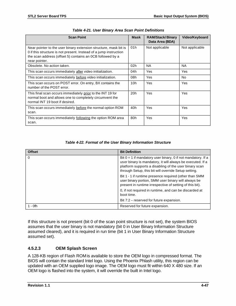
STL2 Server Board TPS Basic Input Output System (BIOS)
Revision 1.1
4-47
Table 4-21. User Binary Area Scan Point Definitions
Scan Point Mask RAM/Stack/ Binary Data Area (BDA)
Video/Keyboard
Near pointer to the user binary extension structure, mask bit is 0 if this structure is not present. Instead of a jump instruction the scan address (offset 5) contains an 0CB followed by a near pointer.
01h Not applicable Not applicable
Obsolete. No action taken. 02h NA NA
This scan occurs immediately after video initialization. 04h Yes Yes
This scan occurs immediately before video initialization. 08h Yes No
This scan occurs on POST error. On entry, BX contains the number of the POST error.
10h Yes Yes
This final scan occurs immediately prior to the INT 19 for normal boot and allows one to completely circumvent the normal INT 19 boot if desired.
20h Yes Yes
This scan occurs immediately before the normal option ROM scan.
40h Yes Yes
This scan occurs immediately following the option ROM area scan.
80h Yes Yes
Table 4-22. Format of the User Binary Information Structure
Offset Bit Definition
0 Bit 0 = 1 if mandatory user binary, 0 if not mandatory. If a user binary is mandatory, it will always be executed. If a platform supports a disabling of the user binary scan through Setup, this bit will override Setup setting.
Bit 1 - 1 if runtime presence required (other than SMM user binary portion, SMM user binary will always be present in runtime irrespective of setting of this bit).
0, if not required in runtime, and can be discarded at boot time.
Bit 7:2 – reserved for future expansion.
1 - 0fh Reserved for future expansion.
If this structure is not present (bit 0 of the scan point structure is not set), the system BIOS assumes that the user binary is not mandatory (bit 0 in User Binary Information Structure assumed cleared), and it is required in run time (bit 1 in User Binary Information Structure assumed set).
4.5.2.3 OEM Splash Screen
A 128-KB region of Flash ROM is available to store the OEM logo in compressed format. The BIOS will contain the standard Intel logo. Using the Phoenix Phlash utility, this region can be updated with an OEM supplied logo image. The OEM logo must fit within 640 X 480 size. If an OEM logo is flashed into the system, it will override the built in Intel logo.

Basic Input Output System (BIOS) STL2 Server Board TPS
Revision 1.1 4-48
Intel supplies utilities that will compress and convert a 16 color bitmap file into a logo file suitable for Phoenix8 Phlash.
4.5.3 Language Area The system BIOS language area can be updated only by updating the entire BIOS. The STL2 platform supports English, Spanish, French, German, and Italian. Intel provides translations for all the strings in five languages. These languages are selectable using Setup.
4.5.4 Recovery Mode In the case of a corrupt or an unsuccessful update of the system BIOS, the STL2 can boot in recovery mode. To place STL2 into recovery mode, move the boot option jumper (jumper block 1J15 pins 9-10) to the recovery boot position. By default and for normal operation, pins 9 and 10 are not jumpered.
Recovery mode requires at least 8 MB of RAM in the first DIMM socket, and drive A: must be set up to support a 3.5-inch, 1.44-MB floppy drive. (Note: the system requires 64 MB to boot). This is the mode of last resort, used only when the main system BIOS will not come up. In recovery mode operation, PHLASH (in non-interactive mode only) automatically updates only the main system BIOS. PHLASH senses that STL2 is in recovery mode and automatically attempts to update the system BIOS
Before powering up the system, the user must obtain a bootable diskette that contains a copy of the BIOS recovery files. This is created by running the “crisdisk.bat” from the compressed recovery file distributed with the BIOS.
Note: During recovery mode, video will not be initialized and many high-pitched beep tones will be heard. The entire process takes two to four minutes. When the process is completed, the tones will stop. The user may see a “Checksum error” on the first boot after updating the BIOS. This is normal and should correct itself after the first boot.
If a failure occurs, it is most likely that of the system BIOS .ROM file is corrupt or missing.
After a successful update, power down the system and remove the jumper from pins 9-10. Power up the system. Verify that the BIOS version number matches the version of the entire BIOS used in the original attempt to update.
4.6 Error Messages and Error Codes The system BIOS displays error messages on the video screen. Prior to video initialization, beep codes inform the user of errors. POST error codes are logged in the event log. The BIOS displays POST error codes on the video monitor.
Following are definitions of POST error codes, POST beep codes, and system error messages.
4.6.1 POST Codes After the video adapter has been successfully initialized, the BIOS indicates the current testing phase during POST by writing a 2-digit hex code to I/O location 80h. If a Port-80h card (Postcard*) is installed, it displays this 2-digit code on a pair of hex display LEDs.
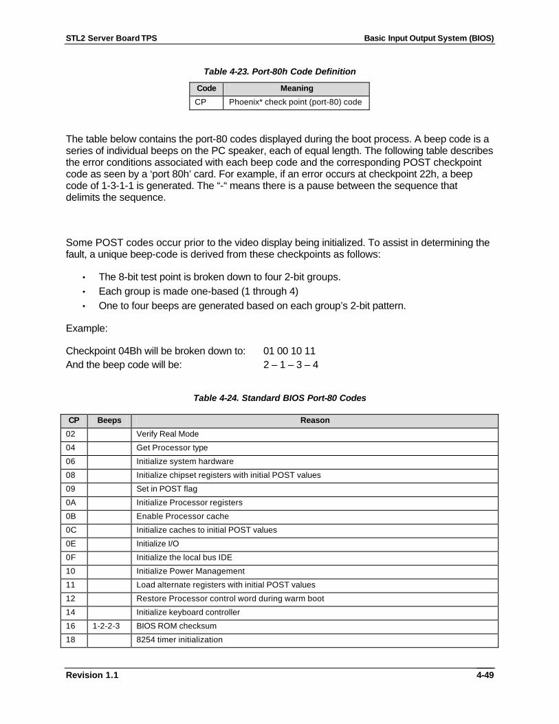
STL2 Server Board TPS Basic Input Output System (BIOS)
Revision 1.1
4-49
Table 4-23. Port-80h Code Definition
Code Meaning
CP Phoenix* check point (port-80) code
The table below contains the port-80 codes displayed during the boot process. A beep code is a series of individual beeps on the PC speaker, each of equal length. The following table describes the error conditions associated with each beep code and the corresponding POST checkpoint code as seen by a ‘port 80h’ card. For example, if an error occurs at checkpoint 22h, a beep code of 1-3-1-1 is generated. The “-“ means there is a pause between the sequence that delimits the sequence.
Some POST codes occur prior to the video display being initialized. To assist in determining the fault, a unique beep-code is derived from these checkpoints as follows:
• The 8-bit test point is broken down to four 2-bit groups. • Each group is made one-based (1 through 4) • One to four beeps are generated based on each group’s 2-bit pattern.
Example:
Checkpoint 04Bh will be broken down to: 01 00 10 11 And the beep code will be: 2 – 1 – 3 – 4
Table 4-24. Standard BIOS Port-80 Codes
CP Beeps Reason
02 Verify Real Mode
04 Get Processor type
06 Initialize system hardware
08 Initialize chipset registers with initial POST values
09 Set in POST flag
0A Initialize Processor registers
0B Enable Processor cache
0C Initialize caches to initial POST values
0E Initialize I/O
0F Initialize the local bus IDE
10 Initialize Power Management
11 Load alternate registers with initial POST values
12 Restore Processor control word during warm boot
14 Initialize keyboard controller
16 1-2-2-3 BIOS ROM checksum
18 8254 timer initialization

Basic Input Output System (BIOS) STL2 Server Board TPS
Revision 1.1 4-50
CP Beeps Reason
1A 8237 DMA controller initialization
1C Reset Programmable Interrupt Controller
20 1-3-1-1 Test DRAM refresh
22 1-3-1-3 Test 8742 Keyboard Controller
24 Set ES segment register to 4 GB
28 1-3-3-1 Autosize DRAM, system BIOS stops execution here if the BIOS does not detect any usable memory DIMMs
2A Clear 8 MB base RAM
2C 1-3-4-1 Base RAM failure, BIOS stops execution here if entire memory is bad
32 Test Processor bus-clock frequency
34 Test CMOS
35 RAM Initialize alternate chipset registers
36 Warm start shut down
37 Reinitialize the chipset
38 Shadow system BIOS ROM
39 Reinitialize the cache
3A Autosize cache
3C Configure advanced chipset registers
3D Load alternate registers with CMOS values
40 Set Initial Processor speed new
42 Initialize interrupt vectors
44 Initialize BIOS interrupts
46 2-1-2-3 Check ROM copyright notice
47 Initialize manager for PCI Option ROMs
48 Check video configuration against CMOS
49 Initialize PCI bus and devices
4A Initialize all video adapters in system
4B Display QuietBoot screen
4C Shadow video BIOS ROM
4E Display copyright notice
50 Display Processor type and speed
52 Test keyboard
54 Set key click if enabled
55 USB initialization
56 Enable keyboard
58 2-2-3-1 Test for unexpected interrupts
5A Display prompt "Press F2 to enter SETUP"
5C Test RAM between 512 and 640 k
60 Test extended memory
62 Test extended memory address lines
64 Jump to UserPatch1
66 Configure advanced cache registers
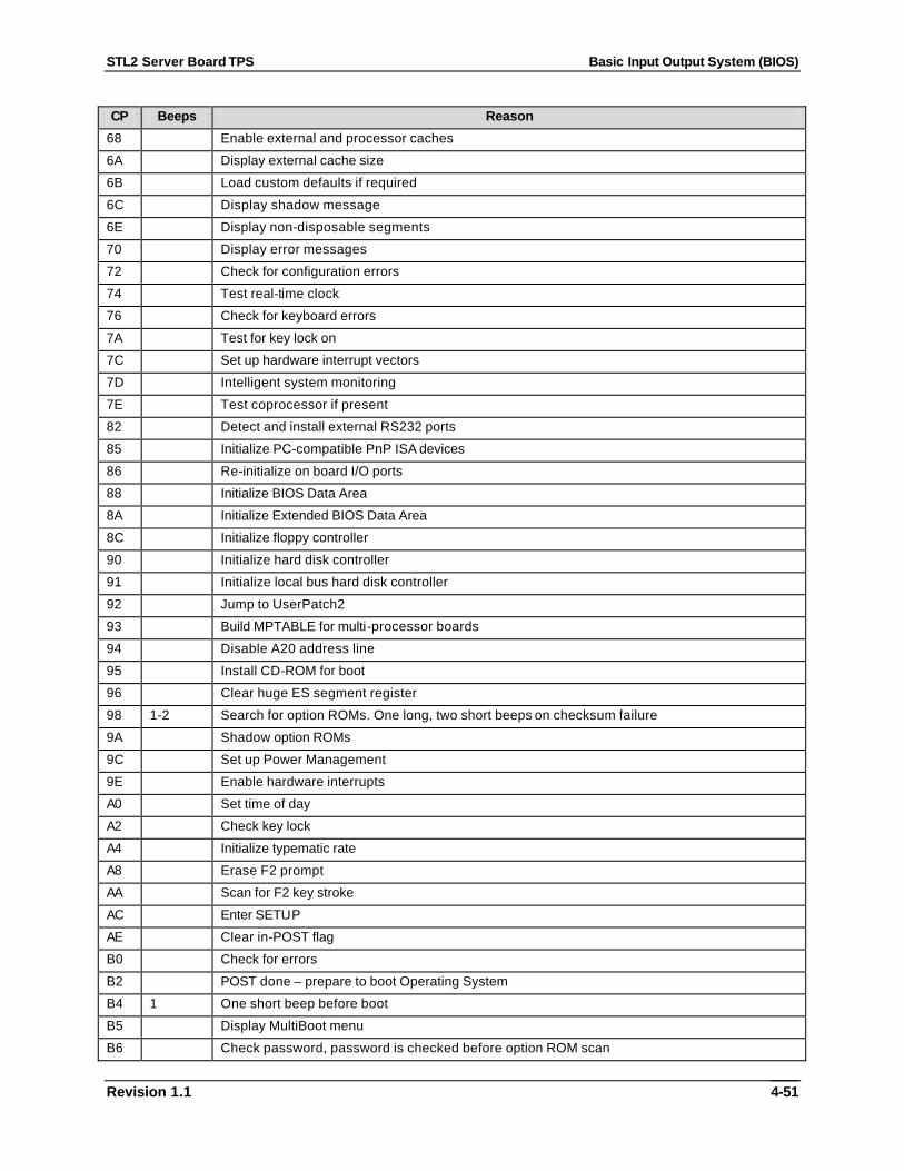
STL2 Server Board TPS Basic Input Output System (BIOS)
Revision 1.1
4-51
CP Beeps Reason
68 Enable external and processor caches
6A Display external cache size
6B Load custom defaults if required
6C Display shadow message
6E Display non-disposable segments
70 Display error messages
72 Check for configuration errors
74 Test real-time clock
76 Check for keyboard errors
7A Test for key lock on
7C Set up hardware interrupt vectors
7D Intelligent system monitoring
7E Test coprocessor if present
82 Detect and install external RS232 ports
85 Initialize PC-compatible PnP ISA devices
86 Re-initialize on board I/O ports
88 Initialize BIOS Data Area
8A Initialize Extended BIOS Data Area
8C Initialize floppy controller
90 Initialize hard disk controller
91 Initialize local bus hard disk controller
92 Jump to UserPatch2
93 Build MPTABLE for multi-processor boards
94 Disable A20 address line
95 Install CD-ROM for boot
96 Clear huge ES segment register
98 1-2 Search for option ROMs. One long, two short beeps on checksum failure
9A Shadow option ROMs
9C Set up Power Management
9E Enable hardware interrupts
A0 Set time of day
A2 Check key lock
A4 Initialize typematic rate
A8 Erase F2 prompt
AA Scan for F2 key stroke
AC Enter SETUP
AE Clear in-POST flag
B0 Check for errors
B2 POST done – prepare to boot Operating System
B4 1 One short beep before boot
B5 Display MultiBoot menu
B6 Check password, password is checked before option ROM scan

Basic Input Output System (BIOS) STL2 Server Board TPS
Revision 1.1 4-52
CP Beeps Reason
B7 ACPI initialization
B8 Clear global descriptor table
BC Clear parity checkers
BE Clear screen (optional)
BF Check virus and backup reminders
C0 Try to boot with INT 19
C8 Forced shutdown
C9 Flash recovery
DO Interrupt handler error
D2 Unknown interrupt error
D4 Pending interrupt error
D6 Initialize option ROM error
D8 Shutdown error
DA Extended Block Move
DC Shutdown 10 error
Table 4-25. Recovery BIOS Port-80 Codes
CP Beeps Reason
E0 Initialize chip set
E1 Initialize bridge
E2 Initialize processor
E3 Initialize timer
E4 Initialize system I/O
E5 Check forced recovery boot
E6 Validate checksum
E7 Go to BIOS
E8 Initialize processors
E9 Set 4 GB segment limits
EA Perform platform initialization
EB Initialize PIC and DMA
EC Initialize memory type
ED Initialize memory size
EE Shadow boot block
EF Test system memory
F0 Initialize interrupt services
F1 Initialize real time clock
F2 Initialize video
F3 Initialize beeper

STL2 Server Board TPS Basic Input Output System (BIOS)
Revision 1.1
4-53
CP Beeps Reason
F4 Initialize boot
F5 Restore segment limits to 64 KB
F6 Boot mini DOS
F7 Boot full DOS
4.6.2 POST Error Codes and Messages The following table defines POST error codes and their associated messages. The BIOS prompts the user to press a key in case of a serious error. Some error messages are preceded by the string "Error” to highlight that the system might be malfunctioning. All POST errors and warnings are logged in the system event log unless it is full.
Table 4-26. POST Error Messages and Codes
Code Error Message Failure Description
0200: Failure Fixed Disk hard disk error
0210: Stuck Key Keyboard connection error
0211: Keyboard error Keyboard failure
0212: Keyboard Controller Failed Keyboard Controller Failed
0213: Keyboard locked– Unlock key switch Keyboard locked
0220: Monitor type does not match CMOS– Run SETUP Monitor type does not match CMOS
0230: System RAM Failed at offset System RAM error Offset address
0231: Shadow RAM Failed at offset Shadow RAM Failed Offset address
0232: Extend RAM Failed at address line Extended RAM failed Offset address
0233: Memory type mixing detected Memory type mixing detected
0234: Single – bit ECC error Memory 1 bit error detected
0235: Multiple- bit ECC error Memory multiple-bit error detected
0250: System battery is dead – Replace and run SETUP NVRAM battery dead
0251: System CMOS checksum bad – Default configuration used
CMOS checksum error
0252: Password checksum bad - Passwords cleared
0260: System timer error System timer error
0270: Real time clock error RTC error
0271: Check date and time setting RTC time setting error
02B0: Diskette drive A error
02B2: Incorrect Drive A type – run SETUP Incorrect Drive A type
02D0: System cache error – Cache disabled Processor cache error
0B00: Rebooted during BIOS boot at Post Code
0B1B: PCI System Error on Bus/Device/Function PCI system error in Bus/device/Function
0B1C: PCI Parity Error in Bus/Device/Function PCI system error in Bus/device/Function

Basic Input Output System (BIOS) STL2 Server Board TPS
Revision 1.1 4-54
Code Error Message Failure Description
0B50: CPU#1 with error taken offline Failed Processor#1 because an error was detected
0B51: CPU#2 with error taken offline Failed Processor#2 because an error was detected
0B5F: Forced to use CPU with error An error detected in the entire processor
0B60: DIMM group #1 has been disabled Memory error, memory group #1 failed
0B61: DIMM group #2 has been disabled Memory error, memory group #2 failed
0B62: DIMM group #3 has been disabled Memory error, memory group #3 failed
0B63: DIMM group #4 has been disabled Memory error, memory group #4 failed
0B6F: DIMM group with error is enabled An error detected in all the memory
0B70: The error occurred during temperature sensor reading Error while detecting a temperature failure.
0B71: System temperature out of the range Temperature error detected.
0B74: The error occurred during voltage sensor reading Error while detecting voltage
0B75: System voltage out of the range System voltage error
0B7C: The error occurred during redundant power module confirmation
The error occurred while retrieving the power information
0B80: BMC Memory Test Failed BMC device (chip) failed
0B81: BMC Firmware Code Area CRC check failed
0B82: BMC core Hardware failure
0B83: BMC IBF or OBF check failed Access to BMC address failed
0B90: BMC Platform Information Area corrupted. BMC device(chip) failed
0B91: BMC update firmware corrupted.
0B92: Internal Use Area of BMC FRU corrupted. SROM storing chassis information failed
(Available for use except for FRU command and EMP function)
0B93: BMC SDR Repository empty. BMC device (chip) failed
0B94: Intelligent Platform Management Bus (IPMB) signal lines do not respond.
SMC(Satellite Management Controller) failed
(Available for use except for the access function to SMC via IPMB)
0B95 BMC FRU device failure. SROM storing chassis information failed
(Available for use except for FRU command and EMP function.)
0B96 BMC SDR Repository failure. BMC device (chip) failed
0B97 BMC SEL device failure.
0BB0: SMBIOS – SROM data read error SROM data read error
0BB1: SMBIOS – SROM data checksum bad Bad checksum of SROM data
0BD0: 1st SMBus device address not acknowledged. Some SMBus device (chip) failed
0BD1: 1st SMBus device Error detected.
0BD2: 1st SMBus timeout.
N/A Expansion ROM not initialized. PCI Expansion ROM card not initialized
N/A Invalid System Configuration Data System configuration data destroyed
N/A System Configuration Data Read Error System configuration data read error
N/A Resource Conflict PCI card resource is not mapped correctly.

STL2 Server Board TPS Basic Input Output System (BIOS)
Revision 1.1
4-55
Code Error Message Failure Description
N/A System Configuration Data Write error System configuration data write error
N/A Warning: IRQ not configured PCI interrupt is not configured correctly.
8503: Incorrect memory speed in location: XX, XX, … Non-PC133 DIMMs have been installed in slots XX, XX, …
A beep code is a series of individual beeps on the PC speaker, each of equal length. The following table describes the error conditions associated with each beep code and the corresponding POST check point code as seen by a port 80h card. For example, if an error occurs at checkpoint 22h, a beep code of 1-3-1-1 is generated. The beep codes 1-1-1-1, 1-5-1-1, 1-5-2-1 and 1-5-3-1 are reserved for BMC usage.
Table 4-27. POST Error Conditions and Beep Codes
Beeps Error Cause Recommended Action
1-2-2-3 ROM Checksum Error — Change system board
1-3-1-1 DRAM Refresh Test Error — Change memory DIMM's
1-3-1-3 Keyboard Controller Test Error — Change system board
1-3-3-1 Memory Not Detected No memory.
Can not write to memory
Verify DIMM installation.
Change memory DIMM's
Memory Capacity Check Error No memory.
Can not write to memory
Verify DIMM installation.
Change memory DIMM's
1-3-4-1 DRAM Address Test Error Memory address signal failure Change DIMM or M/B
1-3-4-3 DRAM Test low byte Error Memory data signal failure (low) Change DIMM or M/B
1-4-1-1 DRAM Test high byte Error Memory data signal failure (high) Change DIMM or M/B
1-4-3-3 All Memory Group Errors — —
2-1-2-3 BIOS ROM Copy-Write Test Error Error with Shadow RAM Change system board
2-2-3-1 Unexpected Interrupt Test Error Unexpected interrupt Change CPU or system board
2-3-1-3 All Memory Group Errors Memory address signal failure Change DIMM or M/B
3-3-1-4 Memory Not Detected — —
1-2 Option ROM Initialization Error Failure to initialize Option ROM BIOS
Change system board or option board
1-2 Video configuration fails Failure to initialize VGA BIOS Change option video board or system board
1-2 OPTION ROM Checksum Error Failure to initialize Option BIOS Change M/B or option board

Basic Input Output System (BIOS) STL2 Server Board TPS
Revision 1.1 4-56
4.7 Identifying BIOS and BMC Revision Levels The following sections provide information to help identify a system's current BIOS and BMC revision levels.
4.7.1 BIOS Revision Level Identification During system POST, which runs automatically when the system is powered on, the monitor displays several messages, one of which identifies the BIOS revision level currently loaded on the system (see the following example).
Phoenix BIOS 4.0 Release 6.0.250A
In the example above, BIOS 6.0.250A is the current BIOS revision level loaded on the system.
Note: Press the Esc key to see the diagnostic messages.
Note: The BIOS Revision Level stated in the example might not reflect the actual BIOS setting in any particular system.
4.7.2 BMC Revision Level Identification During system POST, which runs automatically when the system is powered on, system diagnostics are run. Following the memory test diagnostic, several messages appear to inform the user that the mouse was detected and system configuration data updated. The BMC messages follow these.
To identify the system's current BMC revision level, see the following example.
Base Board Management Controller Device ID :01 Device Revision :00 IPMI Version :1.0 Firmware Revision :00.60 Self Test Result :
In the example above, Firmware Revision 00.60 is the current BMC revision level loaded on the system.
Note: Press the Esc key to see the diagnostic messages.
Note: The Firmware Revision level in the example might not reflect the actual BMC revision level in any particular system.
4.8 Adaptec SCSI Utility The Adaptec SCSI Utility detects the SCSI host adapters on the server board. The Adaptec SCSI Utility is used to:
• Change default values • Check and/or change SCSI device settings that may conflict with those of other devices
in the server.
STL2 Server Board TPS Basic Input Output System (BIOS)
Revision 1.1
4-57
4.8.1 Running the SCSI Utility The user can access the Adaptec SCSI Utility when the system is powered on or rebooted. To run the Adaptec SCSI utility, perform the following procedure.
1. Power-on or reboot the system.
2. At the message to “Press Ctrl-A to run SCSI Utility”, press Ctrl+A.
3. Choose the host adapter that needs to be configured.
4. The SCSI utility starts. When the Adaptec SCSI Utility detects more than one AIC-78xx host adapter, it displays a selection menu listing the bus and device number of each adapter. When the selection menu appears, select the channel that should be configured as follows.
Table 4-28. Channel Configuration
Bus: Device: Channel Selected SCSI Adapter
01: 04: A1 AIC*7899
01: 04: B AIC7899
Note:
1. Internal SCSI Connector
When the adapter is selected, the following options display.
Table 4-29. Adapter Selection Options
Menu Description
Configure/View Host Adapter Settings Configure host adapter and device settings.
SCSI Disk Utilities The utility scans the SCSI bus for SCSI devices and reports a description of each device. Run these utilities before configuring SCSI devices.
To format a disk, verify disk media, or display a list of devices and their SCSI IDs, select “SCSI Disk Utilities”. To configure the adapter or a device, select “Configure/View Host Adapter Settings.”
4.8.2 Adaptec SCSI Utility Configuration Settings The following keys are active for all Adaptec SCSI Utility screens.
Table 4-30. Active Keys for SCSI Utility Screens

Basic Input Output System (BIOS) STL2 Server Board TPS
Revision 1.1 4-58
Key Action
Arrows Up and down arrows move from one parameter to another within a screen.
ENTER Displays options for a configurable parameter. Selects an option.
ESC Moves back to previous screen or parameter or EXIT if at the Main menu.
F5 Switches between color and monochrome.
F6 Resets to host adapter defaults.
The following table shows the normal settings for the Adaptec SCSI Utility and provides a place to record any changes made to these settings.
Table 4-31. Adaptec SCSI Utility Setup Configurations
Option Recommended Setting or Display Only
User Setting
SCSI Bus Interface Definitions
Host Adapter SCSI ID 7
SCSI Parity Checking Enabled
Host Adapter SCSI Termination Enabled
Additional Options
Boot Device Options Press Enter for menu
Boot Channel A First
Boot SCSI ID 0
Boot Logical Unit Number (LUN) Number 0
SCSI Device Configuration Press Enter for menu
Sync Transfer Rate (MBps) 160
Initiate Wide Negotiation Yes
Enable Disconnection Yes
Send Start Unit Command Yes
Enable Write Back Cache No
BIOS Multiple LUN Support No 1
Include in BIOS Scan Yes 1
Advanced Configuration Options Press Enter for menu.
Plug-and-Play SCAM Support Disabled
Reset SCSI Bus at IC Initialization Enabled
Display <Ctrl-A> Messages During BIOS Initialization Enabled
Extended BIOS Translation for DOS Drives >1 Gbyte Enabled
Verbose/Silent Mode Verbose
Host Adapter BIOS (Configuration Utility Reserves BIOS Space)
Enabled1
Domain Validation Enabled
Support Removable Disks Under BIOS as Fixed Disks Disabled1, 2
BIOS Support for Int13 Extensions Enabled1
STL2 Server Board TPS Basic Input Output System (BIOS)
Revision 1.1
4-59
Notes:
1. No effect if BIOS is disabled.
2. Do not remove media from a removable media drive if it is under BIOS control.
4.8.3 Exiting Adaptec SCSI Utility To exit the Adaptec SCSI Utility, the user presses the Esc key several times, until a message prompts him / her to exit. If changes have been made, the user is prompted to save them before exiting.

STL2 Server Board Architecture Overview STL2 Server Board TPS
4-60 Revision 1.1
< This page intentionally left blank >
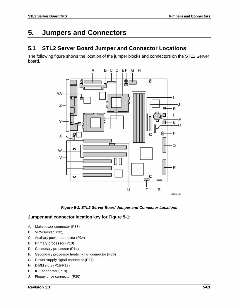
STL2 Server Board TPS Jumpers and Connectors
Revision 1.1
5-61
5. Jumpers and Connectors
5.1 STL2 Server Board Jumper and Connector Locations The following figure shows the location of the jumper blocks and connectors on the STL2 Server board.
Figure 5-1. STL2 Server Board Jumper and Connector Locations
Jumper and connector location key for Figure 5-1:
A. Main power connector (P33)
B. VRM socket (P32)
C. Auxiliary power connector (P34)
D. Primary processor (P13)
E. Secondary processor (P14)
F. Secondary processor heatsink fan connector (P36)
G. Power supply signal connector (P37)
H. DIMM slots (P15-P18)
I. IDE connector (P19)
J. Floppy drive connector (P20)

Jumpers and Connectors STL2 Server Board TPS
Revision 1.1 5-62
K. Two pin speaker connector (P31)
L. System fan connector FAN3A (P29)
M. Battery
N. System fan connector FAN2A (P27)
O. Front panel connector(P23)
P. Four pin speaker connector (P25)
Q. Ultra Single Ended (SE) SCSI connector (P9)
R. Ultra160 LVD SCSI connector (P8)
S. Configuration jumper block (1L4)
T. Configuration jumper block (1J15)
U. CPU speed jumper block (5E1)
V. 33-MHz/32-bit PCI connectors
W. 66-MHz/64-bit PCI connectors
X. Chassis intrusion connector (pins 1-2 of 6A)
Y. System fan connector FAN1 (P11)
Z. I/O ports
AA. Primary processor heatsink fan connector (P12)
The following diagram shows the location of the connectors on the STL2 server board I/O panel.
Figure 5-2. I/O Back Panel Connectors
I/O Back Panel location key for Figure 5-1:
A. USB connectors
B. Serial port 2 connector
C. Serial port 1 connector
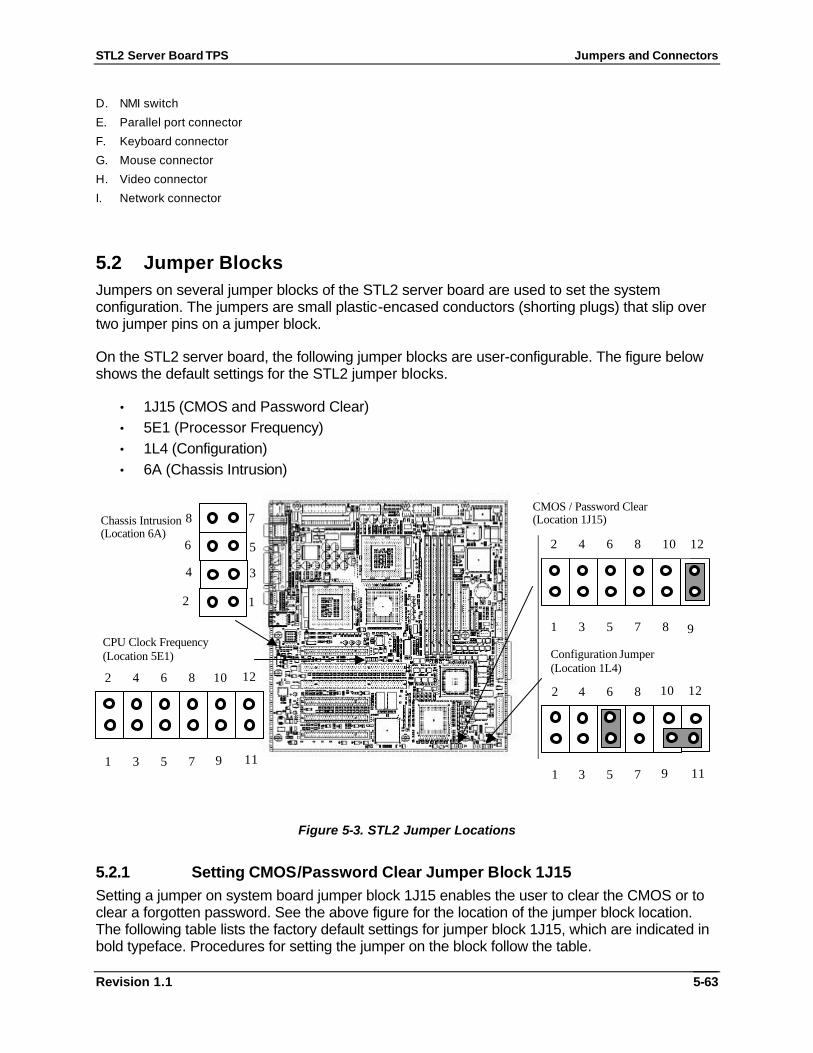
STL2 Server Board TPS Jumpers and Connectors
Revision 1.1
5-63
D. NMI switch
E. Parallel port connector
F. Keyboard connector
G. Mouse connector
H. Video connector
I. Network connector
5.2 Jumper Blocks Jumpers on several jumper blocks of the STL2 server board are used to set the system configuration. The jumpers are small plastic-encased conductors (shorting plugs) that slip over two jumper pins on a jumper block.
On the STL2 server board, the following jumper blocks are user-configurable. The figure below shows the default settings for the STL2 jumper blocks.
• 1J15 (CMOS and Password Clear) • 5E1 (Processor Frequency) • 1L4 (Configuration) • 6A (Chassis Intrusion)
CPU Clock Frequency(Location 5E1)
CMOS / Password Clear(Location 1J15)
2 84 6 10
31
12
875 9
Configuration Jumper(Location 1L4)
1 3
2
5
6
7
4 8 10 12
9 111 3
2
5
6
7
4 8 10 12
9 11
Chassis Intrusion(Location 6A)
12
34
56
78
Figure 5-3. STL2 Jumper Locations
5.2.1 Setting CMOS/Password Clear Jumper Block 1J15 Setting a jumper on system board jumper block 1J15 enables the user to clear the CMOS or to clear a forgotten password. See the above figure for the location of the jumper block location. The following table lists the factory default settings for jumper block 1J15, which are indicated in bold typeface. Procedures for setting the jumper on the block follow the table.
Jumpers and Connectors STL2 Server Board TPS
Revision 1.1 5-64
Table 5-1. Jumper Block 1J15 Settings
Jumper Pin Numbers
Function Jumper Position What it does at system reset
1 - 2 CMOS clear Open, Protect Preserves the contents of CMOS
Closed, Erase Clears CMOS
3 - 4 Password protected Open, Normal Preserves the password
Closed, Disable Disables the password
5 - 6 Reserved Open, Not Used No function
7 - 8 Reserved Open, Not Used No function
9 - 10 BIOS Recovery Boot Open, Normal BIOS Recovery Boot disabled. Normal operation.
Closed, Recovery Boot If this jumper is set, BIOS recovery will be attempted from a bootable BIOS recovery floppy diskette.
11 - 12 Spare Closed, Spare Provides a spare jumper
5.2.1.1 Clearing and Changing a Password
Clear and change a password as follows.
1. Power off the system, unplug the power cord, and remove the chassis panel.
2. Use needle nose pliers or your fingers to remove the spare jumper from pins 11-12 on jumper block 1J15.
3. Reinstall the jumper on pins 3-4 (Password Disable) of jumper block 1J15.
4. Reinstall the chassis panel, plug in the power cord(s), and power on the system.
5. While waiting for POST to complete, press the F2 key to enter BIOS setup.
6. This automatically clears all passwords, provided you save and exit the BIOS setup.
7. Power off the system, unplug the power cord(s), and remove the chassis panel.
8. Remove the Password Disable jumper from pins 3-4 and store the jumper on pins 11-12.
9. Replace the chassis panel, plug in the power cord(s), and power on the system.
10. To specify a new password run the BIOS Setup Utility as described earlier in this section.
5.2.1.2 Clearing CMOS
Clear CMOS as follows.
1. Power off the system, unplug the power cord, and remove the chassis panel.
2. Use needle-nose pliers or your fingers to remove the spare jumper from pins 11-12 on jumper block 1J15.
3. Position the jumper over pins 1-2 on jumper block 1J15.
4. Replace the chassis panel, plug in the power cable(s), and power on the system.

STL2 Server Board TPS Jumpers and Connectors
Revision 1.1
5-65
5. After POST completes, power down the system, unplug the power cable(s), and remove the chassis panel.
6. Remove the jumper from pins 1-2 and store the jumper on pins 11-12.
7. Replace the chassis panel and connect system cables.
8. Power on the system, press F2 at the prompt to run the BIOS Setup utility, and select “Get Default Values” at the Exit menu.
5.2.1.3 Perfoming a BIOS Recovery Boot
In the event of BIOS corruption, the following procedure may be used to perform a BIOS Recovery.
1. Obtain the BIOS update file package from Intel’s iBL or http://support.intel.com web site.
2. A file called “crisis.zip” is one of the files included with each STL2 BIOS release file package. Unzip the “crisis.zip” file to a directory on your hard drive.
3. Obtain a blank formatted floppy diskette (the floppy diskette should not be a bootable DOS diskette). Insert the blank formatted floppy diskette in the floppy drive.
4. From the MS-DOS prompt on an MS-DOS system, run the “crisdisk.bat” file from the directory you created on your hard drive. Follow the instructions on the screen to create the BIOS recovery floppy diskette. Note: The BIOS recovery floppy diskette will not be created correctly under the MS-DOS prompt window of a Windows operating system. It is necessary to use a MS-DOS system to create the BIOS recovery floppy diskette.
5. Power off the STL2 system, unplug the power cord, and remove the chassis panel.
6. Remove the spare jumper from pins 11-12 on jumper block 1J15.
7. Reinstall the jumper on pins 9-10 (BIOS Recovery) of jumper block 1J15.
8. Insert the BIOS recovery floppy diskette into the diskette drive.
9. Reinstall the chassis panel, plug in the power cord(s), and power on the system.
10. The screen will remain blank while the BIOS Recovery is performed. A number of beeps will occur during the BIOS update. The floppy drive access light will not turn off when the BIOS recovery is completed. Allow four minutes for the BIOS recovery to complete. If a POST card is installed in a PCI slot during the BIOS recovery, you can tell that the BIOS recovery is complete when code “EC” is displayed. When the BIOS Recovery is complete, it is safe to power off the system.
11. Power off the system, unplug the power cord(s), and remove the chassis panel.
12. Remove the BIOS Recovery jumper from pins 9-10 and store the jumper on pins 11-12.
13. Replace the chassis panel, plug in the power cord(s), and power on the system.
14. Perform a CMOS clear following the BIOS recovery.
5.2.1.4 Setting Processor Frequency Jumper Block 5E1
The jumpers on block 5E1 set the processor speed for the installed processor(s). The following table lists the settings for jumper block 5E1. Procedures for setting the jumpers follow the table.
Jumpers and Connectors STL2 Server Board TPS
Revision 1.1 5-66
NOTE: It is not necessary to set the jumpers on the processor frequency jumper block 5E1 when using production level (SL Spec) processors. The server board will automatically detect the frequency of production processors.
Table 5-2. Jumper Block 5E1 Settings
Processor Frequency ( MHz)
Jumper Settings
1-2 3-4 5-6 7-8
667 Not Jumpered Not Jumpered Jumpered Jumpered
733 Not Jumpered Not Jumpered Jumpered Not Jumpered
800 Jumpered Jumpered Not Jumpered Jumpered
867 Jumpered Jumpered Not Jumpered Not Jumpered
933 Jumpered Not Jumpered Not Jumpered Jumpered
1000 Jumpered Not Jumpered Not Jumpered Not Jumpered
Set the processor frequency jumpers as follows.
1. Power off the system, unplug the power cord.
2. From the “Jumper Block 5E1 Settings” table, select the processor frequency matching the installed processor.
3. Move the jumpers to the settings shown in the “Jumper Block 5E1 Settings” table.
4. Reinstall the left panel, plug in the power cord(s), and power on the system.
The following table lists the factory default settings for jumper block 5E1, which are indicated in bold typeface.
Table 5-3. Jumper Block 1J15 Default Settings
Jumper Pin Numbers
Function Jumper Position What it does at system reset
1 - 2 Processor Frequency Select Open
3 - 4 Processor Frequency Select Open
5 - 6 Processor Frequency Select Open
7 - 8 Processor Frequency Select Open
9 - 10 133-MHz FSB Open, Enabled Enables 133-MHz FSB
Closed, Disabled Disables 133-MHz FSB
11 - 12 Spread Spectrum Open, Disabled Disables FCC (Spread Spectrum)
Closed, Enabled Enables FCC (Spread Spectrum)
STL2 Server Board TPS Jumpers and Connectors
Revision 1.1
5-67
5.2.2 Setting Configuration Jumper Block 1L4 Setting the jumpers on system board jumper block 1L4 enables the user to configure chassis intrusion sensors, or enable/disable BMC FRB (see the above figure for jumper block location). The following table lists the factory default settings for jumper block 1L4.
Table 5-4. Jumper Block 1L4 Settings
Jumper Pin Numbers Function Jumper Position Function
1 – 2 FRB Open, Enabled Enables FRB
Closed, Disabled Disables FRB
3 – 4 Front Cover Chassis Intrusion Sensor
Open, Enabled Enables Chassis Intrusion sensing. This jumper may be used as a chassis intrusion switch connector.
5 – 6 Side Cover Chassis Intrusion Sensor
Closed, Disabled Disables Chassis Intrusion sensing
Open, Enabled Enables Chassis Intrusion sensing
7 – 8 No Function Open, Not Used No Function
9 – 10 Reserved Open, Not Used No Function
11 – 12 No Function Open, Not Used No Function
9 – 11 Spare Closed, Spare Provides a spare jumper
5.2.3 Setting Configuration Jumper Block 6A Setting the jumpers on system board jumper block 6A enables the user to configure the front cover chassis intrusion sensing. Jumper 6A pins 1-2 may also be used as a chassis intrusion switch connector. The following table lists the factory default settings for jumper block 6A.
Table 5-5. Jumper Block 6A Settings
Jumper Pin Numbers
Function Jumper Position Function
1 – 2 Front Cover Chassis Intrusion Sensor
Open, Enabled Enables Chassis Intrusion sensing. This jumper may be used as a chassis intrusion switch connector.
Closed, Disabled Disables Chassis Intrusion sensing
3 – 4 Reserved Open, Not Used No Function
5 – 6 No Function Open, Not Used No Function
7 – 8 Reserved Open, Not Used No Function
5.3 Connectors This section provides pin information about the connectors on the STL2 server board.
Jumpers and Connectors STL2 Server Board TPS
Revision 1.1 5-68
5.3.1 Main ATX Power Connector (P33)
Table 5-6. Main ATX Power Connector Pinout
Pin Signal Wire color Pin Signal Wire Color
1 +3.3 VDC Orange 13 +3.3 VDC Orange
2 +3.3 VDC Orange 14 -12 VDC Blue
3 COM Black 15 COM Black
4 +5 VDC Red 16 PS-ON_L Green
5 COM Black 17 COM Black
6 +5 VDC Red 18 COM Black
7 COM Black 19 COM Black
8 PWR-GD Grey 20 N.C. N.C.
9 5 VSB Purple 21 +5 VDC Red
10 +12 VDC Yellow 22 +5 VDC Red
11 +12 VDC Yellow 23 +5 VDC Red
12 +3.3 VDC Orange 24 COM Black
5.3.2 Auxilary ATX Power Connector (P34)
Table 5-7. Auxiliary ATX Power Connector Pinout
Pin Signal Wire Color
1 +5 VDC Red
2 +3.3 VDC Orange
3 +3.3 VDC Orange
4 COM Black
5 COM Black
6 COM Black
5.3.3 I2C Power Connector (P37)
Table 5-8. I2C Power Connector Pinout
Pin Signal Pin Signal
1 N.C. 6 N.C.
2 N.C. 7 N.C.
3 +3.3 VDC 8 N.C.
4 N.C. 9 I2C Data
5 N.C. 10 I2C Clock
STL2 Server Board TPS Jumpers and Connectors
Revision 1.1
5-69
5.3.4 System Fan Connectors (P29, P27, P11) • System Fan 1: P11 • System Fan 2: P27 • System Fan 3: P29
Table 5-9. Board Fan Connector Pinout
Pin Signal
1 Fan Sense
2 + 12 VDC
3 COM
5.3.5 Processor Connectors (P12, P36) • Primary Processor Fan 1: P36 • Secondary Processor Fan 2: P12
Table 5-10. Processor Fan Connector Pinout
Pin Signal
1 N.C.
2 + 12 VDC
3 COM
5.3.6 Speaker Connector (P31)
Table 5-11. Speaker Connector Pinout
Pin Signal
1 SPEAKER
2 GND
5.3.7 Speaker Connector (P25)
Table 5-12. Speaker Connector Pinout
Pin Signal
1 SPEAKER
2 GND
3 N.C.
Jumpers and Connectors STL2 Server Board TPS
Revision 1.1 5-70
4 GND
5.3.8 Diskette Drive Connector (P20)
18 3 4
1 17
Figure 5-4. Diskette Drive Connector Pin Diagram
Table 5-13. Diskette Drive Connector Pinout
Pin Signal Pin Signal
1 GND 18 FD_DENSEL
2 GND 19 No Connection
3 GND 20 FD_MDAID
4 GND 21 FD_INDEX_L
5 GND 22 FD_MON0_L
6 GND 23 FD_SEL1_L
7 GND 24 FD_SEL0_L
8 GND 25 FD_MON1_L
9 GND 26 FD_DIR_L
10 GND 27 FD_STEP_L
11 GND 28 FD_WDATA_L
12 GND 29 FD_WGATE_L
13 GND 30 FD_TRK0_L
14 GND 31 FD_WPT_L
15 GND 32 FD_RDATA_L
16 GND 33 FD_SIDE_L
17 GND 34 FD_DCHG_L
5.3.9 SVGA Video Port
Table 5-14. Video Port Connector Pinout
Pin Signal Pin Signal
1 Red 9 NC
STL2 Server Board TPS Jumpers and Connectors
Revision 1.1
5-71
Pin Signal Pin Signal
2 Green 10 GND
3 Blue 11 NC
4 NC 12 DDCDAT
5 GND 13 HSYNC
6 GND 14 VSYNC
7 GND 15 DDCCLK
8 GND
5.3.10 Keyboard and Mouse Connectors The keyboard and mouse connectors are functionally equivalent.
Table 5-15. Keyboard and Mouse Connector Pinouts
Pin Keyboard Signal Pin Mouse Signal
1 KEYDAT 1 MSEDAT
2 GND 2 NC
3 GND 3 GND
4 FUSED_VCC (+5 V) 4 FUSED_VCC (+5 V)
5 KEYCLK 5 MSECLK
6 NC 6 NC
5.3.11 Parallel Port
Table 5-16. Parallel Port Connector Pinouts
Pin Signal Pin Signal
1 STROBE_L 10 ACK_L
2 Data bit 0 11 Busy
3 Data bit 1 12 PE
4 Data bit 2 13 SLCT
5 Data bit 3 14 AUTO_L
6 Data bit 4 15 ERROR_L
7 Data bit 5 16 INIT_L
8 Data bit 6 17 SLCTIN_L
9 Data bit 7 18−25 GND

Jumpers and Connectors STL2 Server Board TPS
Revision 1.1 5-72
5.3.12 Serial Ports COM1 and COM2
Table 5-17. Serial Ports COM1 and COM2 Connector Pinouts
Pin Signal Description
1 DCD Data carrier detected
2 RXD Receive data
3 TXD Transmit data
4 DTR Data terminal ready
5 GND Ground
6 DSR Data set ready
7 RTS Return to send
8 CTS Clear to send
9 RIA Ring indication active
5.3.13 RJ-45 LAN Connector
Table 5-18. RJ-45 LAN Connector Signals
Pin Signal Description
1 TX+ Transmit data plus—the positive signal for the TD differential pair contains the serial output data stream transmitted onto the network
2 TX- Transmit data minus—the negative signal for the TD differential pair contains the same output as pin 1
3 RX+ Receive data plus—the positive signal for the RD differential pair contains the serial input data stream received from the network
4 NC
5 NC
6 RX- Receive data minus—the negative signal for the RD differential pair contains the same input as pin 3
7 NC
8 NC
5.3.14 USB Connectors
Table 5-19. USB Connectors
USB 1 Pin Signal USB 2 Pin Signal
1 +5 VDC 1 +5 VDC
2 USB_P1_N 2 USB_P0_N
3 USB_P1_P 3 USB_P0_P
4 GND 4 GND

STL2 Server Board TPS Jumpers and Connectors
Revision 1.1
5-73
5.3.15 Ultra SCSI Connector (P9)
Table 5-20. Ultra SCSI Connector Pinout
Pin Signal Pin Signal
1-16 GND 49-50 GND
17 TERMPWR 51 TERMPWR
18 TERMPWR 52 TERMPWR
19 NC 53 NC
20-34 GND 54 GND
35 SCD12_L 55 SATN_L
36 SCD13_L 56 GND
37 SCD14_L 57 SBSY_L
38 SCD15_L 58 SACK_L
39 SCDPH_L 59 RESET_L
40 SCD0_L 60 SMSG_L
41 SCD1_L 61 SSEL_L
42 SCD2_L 62 SCD_L
43 SCD3_L 63 SREQ_L
44 SCD4_L 64 SI/O_L
45 SCD5_L 65 SCD8_L
46 SCD6_L 66 SCD9_L
47 SCD7_L 67 SCD10_L
48 SCDP_L 68 SCD11_L
5.3.16 Ultra160 SCSI Connector (P8)
Table 5-21. Ultra160 SCSI Connector
Pin Signal Pin Signal
1 SCDAP12 35 SCDAN12_L
2 SCDAP13 36 SCDAN13_L
3 SCDAP14 37 SCDAN14_L
4 SCDAP15 38 SCDAN15_L
5 SCDAPHP 39 SCDAPHN_L
6 SCDAP0 40 SCDAN0_L
7 SCDAP1 41 SCDAN1_L
8 SCDAP2 42 SCDAN2_L
9 SCDAP3 43 SCDAN3_L
10 SCDAP4 44 SCDAN4_L
11 SCDAP5 45 SCDAN5_L
12 SCDAP6 46 SCDAN6_L
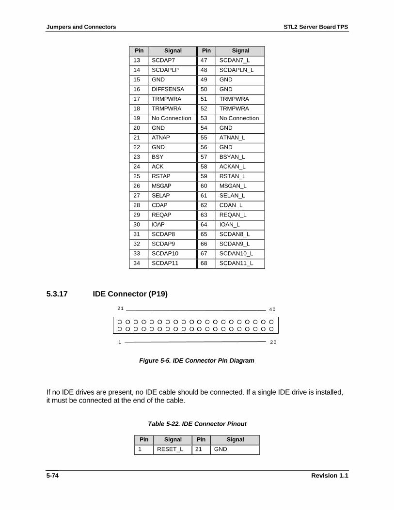
Jumpers and Connectors STL2 Server Board TPS
Revision 1.1 5-74
Pin Signal Pin Signal
13 SCDAP7 47 SCDAN7_L
14 SCDAPLP 48 SCDAPLN_L
15 GND 49 GND
16 DIFFSENSA 50 GND
17 TRMPWRA 51 TRMPWRA
18 TRMPWRA 52 TRMPWRA
19 No Connection 53 No Connection
20 GND 54 GND
21 ATNAP 55 ATNAN_L
22 GND 56 GND
23 BSY 57 BSYAN_L
24 ACK 58 ACKAN_L
25 RSTAP 59 RSTAN_L
26 MSGAP 60 MSGAN_L
27 SELAP 61 SELAN_L
28 CDAP 62 CDAN_L
29 REQAP 63 REQAN_L
30 IOAP 64 IOAN_L
31 SCDAP8 65 SCDAN8_L
32 SCDAP9 66 SCDAN9_L
33 SCDAP10 67 SCDAN10_L
34 SCDAP11 68 SCDAN11_L
5.3.17 IDE Connector (P19)
1 2 0
2 1 4 0
Figure 5-5. IDE Connector Pin Diagram
If no IDE drives are present, no IDE cable should be connected. If a single IDE drive is installed, it must be connected at the end of the cable.
Table 5-22. IDE Connector Pinout
Pin Signal Pin Signal
1 RESET_L 21 GND

STL2 Server Board TPS Jumpers and Connectors
Revision 1.1
5-75
Pin Signal Pin Signal
2 DD7 22 DD8
3 DD6 23 DD9
4 DD5 24 DD10
5 DD4 25 DD11
6 DD3 26 DD12
7 DD2 27 DD13
8 DD1 28 DD14
9 DD0 29 DD15
10 GND 30 No Connection
11 IDEDRQ 31 GND
12 DIOW_L 32 GND
13 DIOR_L 33 GND
14 IORDY 34 GND
15 IDEDAK_L 35 GND
16 IDEIRQ 36 No Connection
17 IDESA1 37 No Connection
18 IDESA0 38 IDESA2
19 IDECS0_L 39 IDECS1_L
20 Keyed 40 GND
5.3.18 32-Bit PCI Connector
Table 5-23. 32-Bit PCI Connector Pinout
Pin Signal Pin Signal Pin Signal Pin Signal
A1 TRST_L B1 -12 V A32 AD16 B32 AD17
A2 +12 V B2 TCK A33 +3.3 V B33 CBE2_L
A3 TMS B3 GND A34 FRAME_L B34 GND
A4 TDI B4 TD0 (NC) A35 GND B35 IRDY_L
A5 +5 V B5 +5 V A36 TRDY_L B36 +3.3 V
A6 INTA_L B6 +5 V A37 GND B37 DEVSEL_L
A7 INTC_L B7 INTB_L A38 STOP_L B38 GND
A8 +5 V B8 INTD_L A39 +3.3 V B39 LOCK_L
A9 Reserved B9 PRSNT1_L A40 SDONE B40 PERR_L
A10 +5 V B10 Reserved A41 SBO_L B41 +3.3 V
A11 Reserved B11 PRSNT2_L A42 GND B42 SERR_L
A12 GND B12 GND A43 PARITY B43 +3.3 V
A13 GND B13 GND A44 AD15 B44 CBE1_L
A14 Reserved B14 Reserved A45 +3.3 V B45 AD14
A15 RST_L B15 GND A46 AD13 B46 GND
A16 +5 V B16 PCICLK A47 AD11 B47 AD12
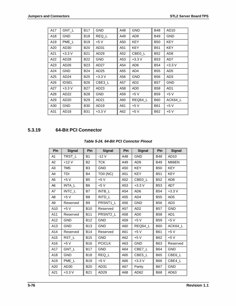
Jumpers and Connectors STL2 Server Board TPS
Revision 1.1 5-76
A17 GNT_L B17 GND A48 GND B48 AD10
A18 GND B18 REQ_L A49 AD9 B49 GND
A19 PME_L B19 +5 V A50 KEY B50 KEY
A20 AD30 B20 AD31 A51 KEY B51 KEY
A21 +3.3 V B21 AD29 A52 CBE0_L B52 AD8
A22 AD28 B22 GND A53 +3.3 V B53 AD7
A23 AD26 B23 AD27 A54 AD6 B54 +3.3 V
A24 GND B24 AD25 A55 AD4 B55 AD5
A25 AD24 B25 +3.3 V A56 GND B56 AD3
A26 IDSEL B26 CBE3_L A57 AD2 B57 GND
A27 +3.3 V B27 AD23 A58 AD0 B58 AD1
A28 AD22 B28 GND A59 +5 V B59 +5 V
A29 AD20 B29 AD21 A60 REQ64_L B60 ACK64_L
A30 GND B30 AD19 A61 +5 V B61 +5 V
A31 AD18 B31 +3.3 V A62 +5 V B62 +5 V
5.3.19 64-Bit PCI Connector
Table 5-24. 64-Bit PCI Connctor Pinout
Pin Signal Pin Signal Pin Signal Pin Signal
A1 TRST_L B1 -12 V A48 GND B48 AD10
A2 +12 V B2 TCK A49 AD9 B49 M66EN
A3 TMS B3 GND A50 KEY B50 KEY
A4 TDI B4 TD0 (NC) A51 KEY B51 KEY
A5 +5 V B5 +5 V A52 CBE0_L B52 AD8
A6 INTA_L B6 +5 V A53 +3.3 V B53 AD7
A7 INTC_L B7 INTB_L A54 AD6 B54 +3.3 V
A8 +5 V B8 INTD_L A55 AD4 B55 AD5
A9 Reserved B9 PRSNT1_L A56 GND B56 AD3
A10 +5 V B10 Reserved A57 AD2 B57 GND
A11 Reserved B11 PRSNT2_L A58 AD0 B58 AD1
A12 GND B12 GND A59 +5 V B59 +5 V
A13 GND B13 GND A60 REQ64_L B60 ACK64_L
A14 Reserved B14 Reserved A61 +5 V B61 +5 V
A15 RST_L B15 GND A62 +5 V B62 +5 V
A16 +5 V B16 PCICLK A63 GND B63 Reserved
A17 GNT_L B17 GND A64 CBE7_L B64 GND
A18 GND B18 REQ_L A65 CBE5_L B65 CBE6_L
A19 PME_L B19 +5 V A66 +3.3 V B66 CBE4_L
A20 AD30 B20 AD31 A67 Parity B67 GND
A21 +3.3 V B21 AD29 A68 AD62 B68 AD63
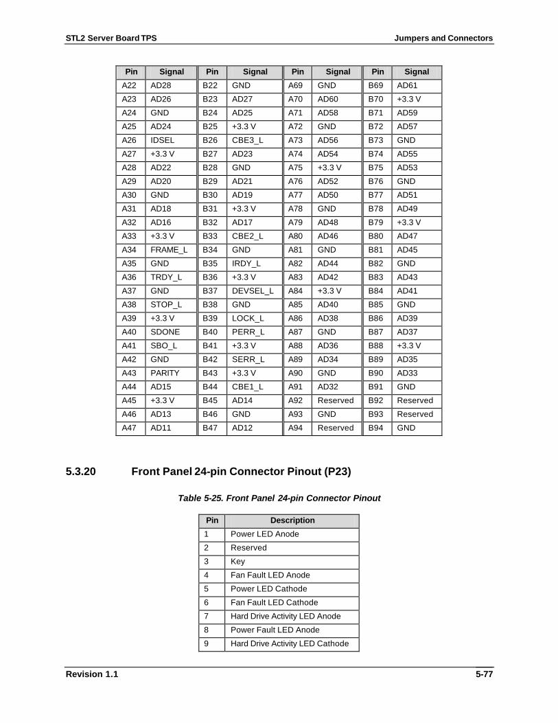
STL2 Server Board TPS Jumpers and Connectors
Revision 1.1
5-77
Pin Signal Pin Signal Pin Signal Pin Signal
A22 AD28 B22 GND A69 GND B69 AD61
A23 AD26 B23 AD27 A70 AD60 B70 +3.3 V
A24 GND B24 AD25 A71 AD58 B71 AD59
A25 AD24 B25 +3.3 V A72 GND B72 AD57
A26 IDSEL B26 CBE3_L A73 AD56 B73 GND
A27 +3.3 V B27 AD23 A74 AD54 B74 AD55
A28 AD22 B28 GND A75 +3.3 V B75 AD53
A29 AD20 B29 AD21 A76 AD52 B76 GND
A30 GND B30 AD19 A77 AD50 B77 AD51
A31 AD18 B31 +3.3 V A78 GND B78 AD49
A32 AD16 B32 AD17 A79 AD48 B79 +3.3 V
A33 +3.3 V B33 CBE2_L A80 AD46 B80 AD47
A34 FRAME_L B34 GND A81 GND B81 AD45
A35 GND B35 IRDY_L A82 AD44 B82 GND
A36 TRDY_L B36 +3.3 V A83 AD42 B83 AD43
A37 GND B37 DEVSEL_L A84 +3.3 V B84 AD41
A38 STOP_L B38 GND A85 AD40 B85 GND
A39 +3.3 V B39 LOCK_L A86 AD38 B86 AD39
A40 SDONE B40 PERR_L A87 GND B87 AD37
A41 SBO_L B41 +3.3 V A88 AD36 B88 +3.3 V
A42 GND B42 SERR_L A89 AD34 B89 AD35
A43 PARITY B43 +3.3 V A90 GND B90 AD33
A44 AD15 B44 CBE1_L A91 AD32 B91 GND
A45 +3.3 V B45 AD14 A92 Reserved B92 Reserved
A46 AD13 B46 GND A93 GND B93 Reserved
A47 AD11 B47 AD12 A94 Reserved B94 GND
5.3.20 Front Panel 24-pin Connector Pinout (P23)
Table 5-25. Front Panel 24-pin Connector Pinout
Pin Description
1 Power LED Anode
2 Reserved
3 Key
4 Fan Fault LED Anode
5 Power LED Cathode
6 Fan Fault LED Cathode
7 Hard Drive Activity LED Anode
8 Power Fault LED Anode
9 Hard Drive Activity LED Cathode
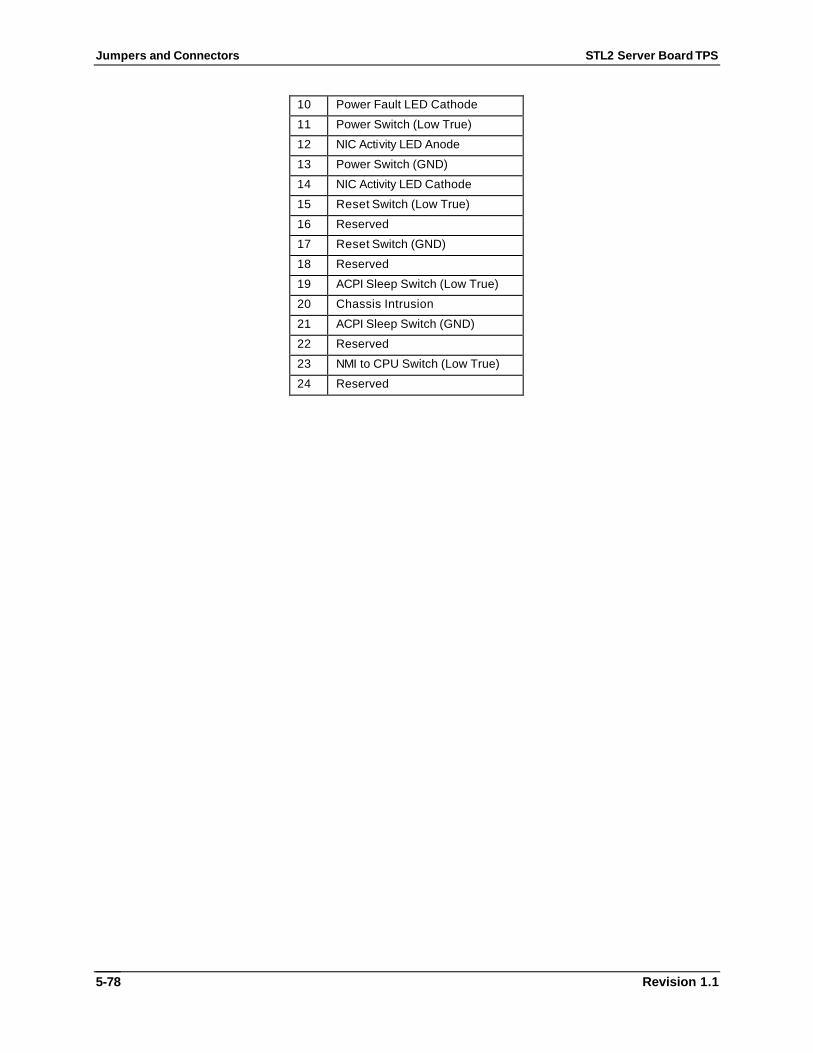
Jumpers and Connectors STL2 Server Board TPS
Revision 1.1 5-78
10 Power Fault LED Cathode
11 Power Switch (Low True)
12 NIC Activity LED Anode
13 Power Switch (GND)
14 NIC Activity LED Cathode
15 Reset Switch (Low True)
16 Reserved
17 Reset Switch (GND)
18 Reserved
19 ACPI Sleep Switch (Low True)
20 Chassis Intrusion
21 ACPI Sleep Switch (GND)
22 Reserved
23 NMI to CPU Switch (Low True)
24 Reserved
STL2 Server Board TPS Jumpers and Connectors
Revision 1.1
5-79
< This page intentionally left blank >
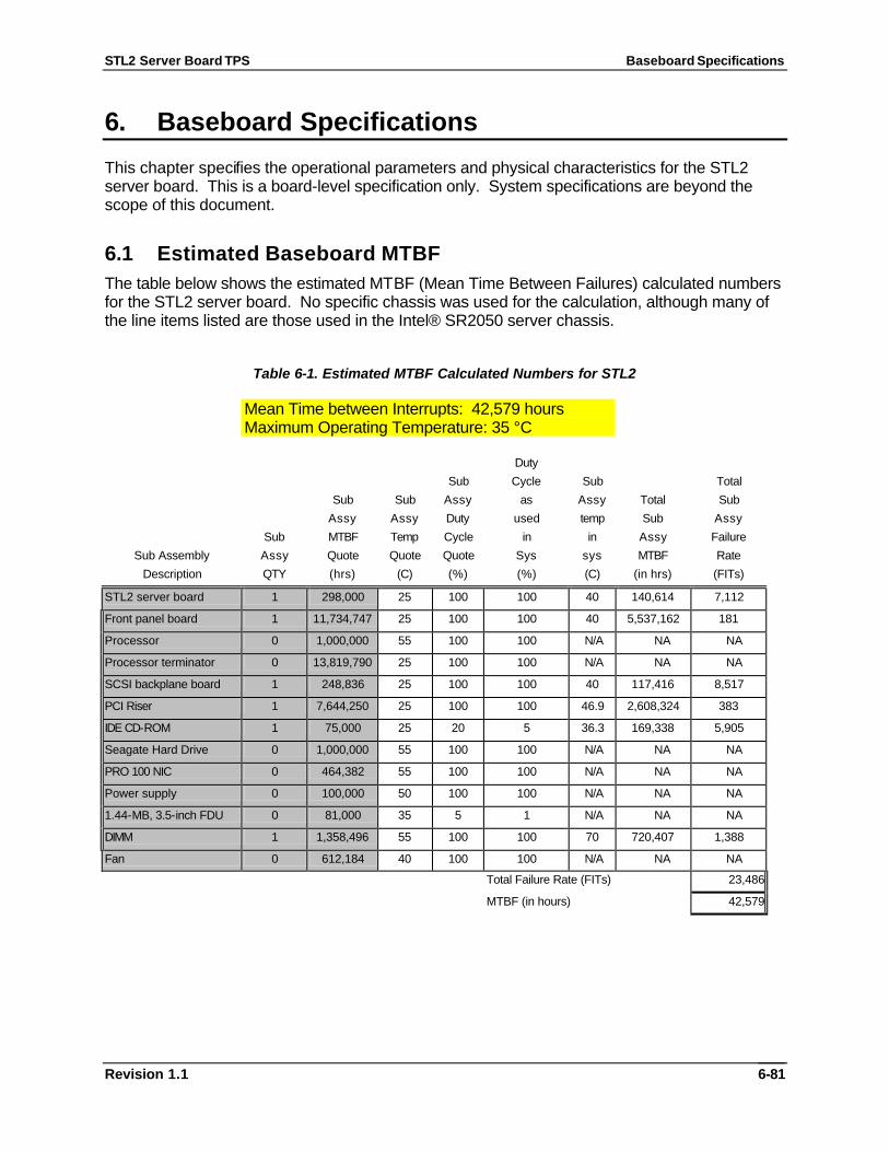
STL2 Server Board TPS Baseboard Specifications
Revision 1.1
6-81
6. Baseboard Specifications
This chapter specifies the operational parameters and physical characteristics for the STL2 server board. This is a board-level specification only. System specifications are beyond the scope of this document.
6.1 Estimated Baseboard MTBF The table below shows the estimated MTBF (Mean Time Between Failures) calculated numbers for the STL2 server board. No specific chassis was used for the calculation, although many of the line items listed are those used in the Intel® SR2050 server chassis.
Table 6-1. Estimated MTBF Calculated Numbers for STL2
Mean Time between Interrupts: 42,579 hours Maximum Operating Temperature: 35 °C Duty
Sub Cycle Sub Total
Sub Sub Assy as Assy Total Sub
Assy Assy Duty used temp Sub Assy
Sub MTBF Temp Cycle in in Assy Failure
Sub Assembly Assy Quote Quote Quote Sys sys MTBF Rate
Description QTY (hrs) (C) (%) (%) (C) (in hrs) (FITs)
STL2 server board 1 298,000 25 100 100 40 140,614 7,112
Front panel board 1 11,734,747 25 100 100 40 5,537,162 181
Processor 0 1,000,000 55 100 100 N/A NA NA
Processor terminator 0 13,819,790 25 100 100 N/A NA NA
SCSI backplane board 1 248,836 25 100 100 40 117,416 8,517
PCI Riser 1 7,644,250 25 100 100 46.9 2,608,324 383
IDE CD-ROM 1 75,000 25 20 5 36.3 169,338 5,905
Seagate Hard Drive 0 1,000,000 55 100 100 N/A NA NA
PRO 100 NIC 0 464,382 55 100 100 N/A NA NA
Power supply 0 100,000 50 100 100 N/A NA NA
1.44-MB, 3.5-inch FDU 0 81,000 35 5 1 N/A NA NA
DIMM 1 1,358,496 55 100 100 70 720,407 1,388
Fan 0 612,184 40 100 100 N/A NA NA
Total Failure Rate (FITs) 23,486
MTBF (in hours) 42,579
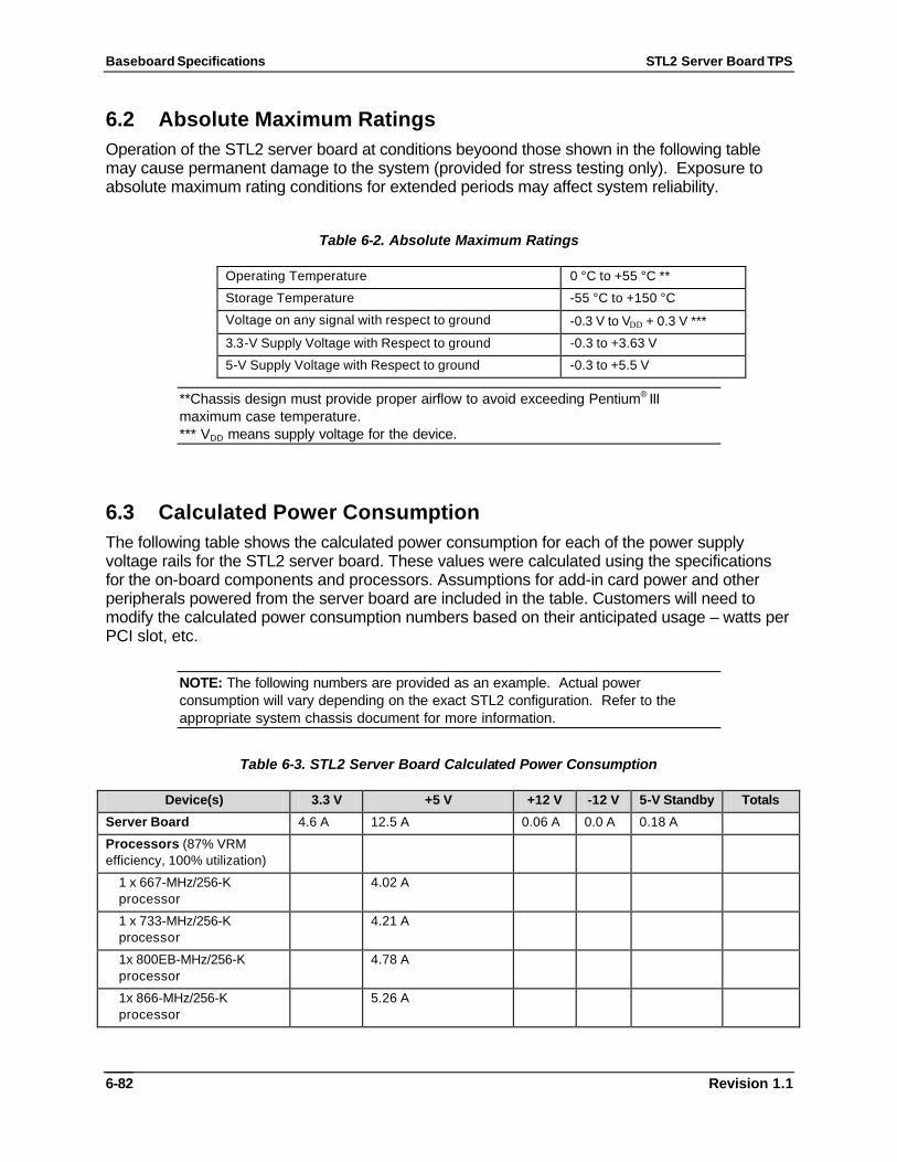
Baseboard Specifications STL2 Server Board TPS
Revision 1.1 6-82
6.2 Absolute Maximum Ratings Operation of the STL2 server board at conditions beyoond those shown in the following table may cause permanent damage to the system (provided for stress testing only). Exposure to absolute maximum rating conditions for extended periods may affect system reliability.
Table 6-2. Absolute Maximum Ratings
Operating Temperature 0 °C to +55 °C **
Storage Temperature -55 °C to +150 °C
Voltage on any signal with respect to ground -0.3 V to VDD + 0.3 V ***
3.3-V Supply Voltage with Respect to ground -0.3 to +3.63 V
5-V Supply Voltage with Respect to ground -0.3 to +5.5 V
**Chassis design must provide proper airflow to avoid exceeding Pentium® III maximum case temperature. *** VDD means supply voltage for the device.
6.3 Calculated Power Consumption The following table shows the calculated power consumption for each of the power supply voltage rails for the STL2 server board. These values were calculated using the specifications for the on-board components and processors. Assumptions for add-in card power and other peripherals powered from the server board are included in the table. Customers will need to modify the calculated power consumption numbers based on their anticipated usage – watts per PCI slot, etc.
NOTE: The following numbers are provided as an example. Actual power consumption will vary depending on the exact STL2 configuration. Refer to the appropriate system chassis document for more information.
Table 6-3. STL2 Server Board Calculated Power Consumption
Device(s) 3.3 V +5 V +12 V -12 V 5-V Standby Totals
Server Board 4.6 A 12.5 A 0.06 A 0.0 A 0.18 A
Processors (87% VRM efficiency, 100% utilization)
1 x 667-MHz/256-K processor
4.02 A
1 x 733-MHz/256-K processor
4.21 A
1x 800EB-MHz/256-K processor
4.78 A
1x 866-MHz/256-K processor
5.26 A

STL2 Server Board TPS Baseboard Specifications
Revision 1.1
6-83
Device(s) 3.3 V +5 V +12 V -12 V 5-V Standby Totals
1x 933-MHz/256-K processor
5.63 A
1x 1-GHz/256-K processor 6.0 A
Memory (Four PC133 Registered GB SDRAM DIMMs)
5.5 A
PCI Connectors
32-bit PCI slots (1 0W per slot on 5 V)
8.0 A 0.4 A
64-bit PCI slots (10 W per slot on 3.3 V)
6.06 A 0.2 A
USB (500mA per connector) 1.00 A
Keyboard/Mouse 0.50 A
SCSI term power Included in board spec.
Fans (Three chassis and two processor)
1.32 A
Total Current 16.16 A 34.0 A 1.38 A 0.0 A 0.78 A Total
Total Power 53.33 W 170.0 W 16.6 W 0.0 W 3.9 W 243.83 W
The total power calculation assumes a system configuration containing dual Pentium® III 1-GHz processors with the VRM for both processors supplied by the 5-V source, four 1-GHz DIMMs, all PCI slots containing 10-W cards, two USB devices, keyboard and mouse, three chassis fans, and two processor fan heat sinks.
6.4 Measured Power Consumption A STL2 FAB 2 server board was configured with dual 866-MHz processors, both supplied by the 5-V voltage regulation modules (VRMs), and four 1-GB PC133 SDRAM DIMMs (Infineon part number HYS72V128320GR).
The system was configured with Microsoft Windows NT 4.0. Test software utilized during the power consumption measurement consisted of the Hipower test suite, used to simulate medium processor activity, and the WinMTA memory stress test suite, used to simulate high memory activity.
The STL2 server board measured power consumption including the memory and processor power is listed in the following table.
Table 6-4. STL2 Server Board Measured Power Consumption
Device(s) 3.3 V +5 V +12 V Total Wattage
Server Board 6.0 A 8.5 A 0.01 A 63.5 W

Baseboard Specifications STL2 Server Board TPS
Revision 1.1 6-84
6.5 Mechanical Specifications The diagram on the following page shows the mechanical specifications of the STL2 server board. All dimensions are in inches. Connectors are dimensioned to pin 1.
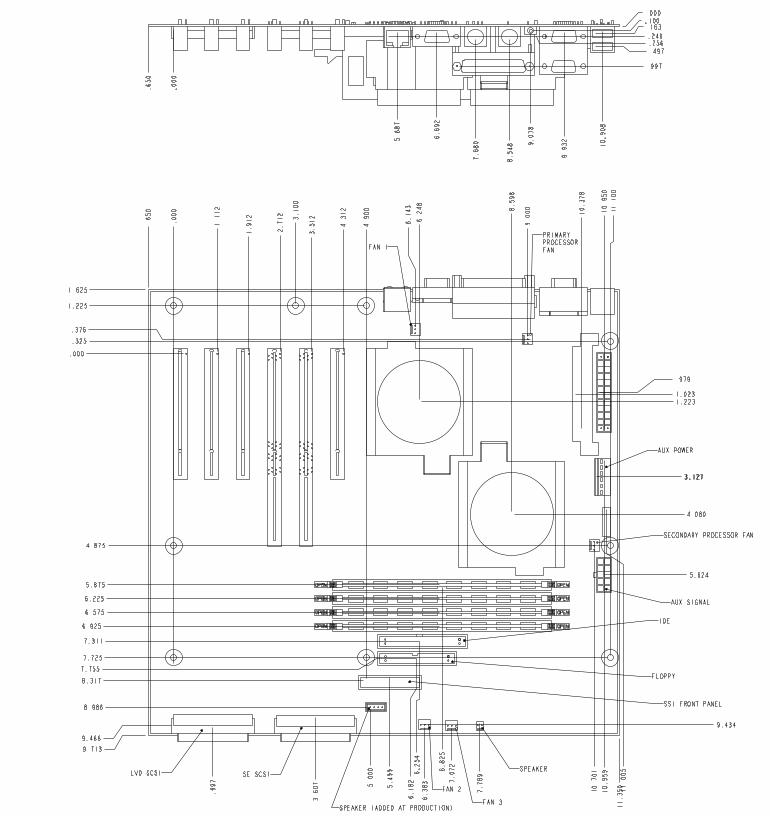

STL2 Server Board Architecture Overview STL2 Server Board TPS
6-86 Revision 1.1
< This page intentionally left blank >

STL2 Server Board TPS Regulatory and Integration Information
Revision 1.1
7-87
7. Regulatory and Integration Information
7.1 Regulatory Compliance The STL2 server board complies with the following safety standard requirements.
Table 7-1. Safety Regulations
Regulation Title
UL 1950/CSA950 Bi-National Standard for Safety of Information Technology Equipment including Electrical Business Equipment. (USA and Canada)
EN 60950 The Standard for Safety of Information Technology Equipment including Electrical Business Equipment. (European Community)
IEC60 950 The Standard for Safety of Information Technology Equipment including Electrical Business Equipment. (International)
EMKO-TSE (74-SEC) 207/94 Summary of Nordic deviations to EN 60950. (Norway, Sweden, Denmark, and Finland)
EU Low Voltage Directive 73/23/ECC Compliance to EU LV Directive via EN60 950 / IEC 60950
The STL2 server board has been tested and verified to comply with the following EMC regulations when installed in a compatible Intel host system. For information on Intel compatible host system(s), refer to Intel’s Server Builder website, or contact your local Intel representative.
Table 7-2. EMC Regulations
Regulation Title
FCC – Class A Title 47 of the Code of Federal Regulations, Parts 2 and 15, Subpart B, pertaining to unintentional radiators. (USA)
ICES-003 – Class A Interference-Causing Equipment Standard, Digital Apparatus, Class A (including CRC c. 1374) (Canada).
CISPR 22 Limits and methods of measurement of Radio Interference Characteristics of Information Technology Equipment. (International)
VCCI – Class A Implementation Regulations for Voluntary Control of Radio Interference by Data Processing Equipment and Electronic Office Machines. (Japan)
EN55022 Limits and methods of measurement of Radio Interference Characteristics of Information Technology Equipment. (Europe)
EN55024 Generic Immunity Standard; currently compliance is determined via testing to IEC 801-2, -3, and -4. (Europe)
EU EMC Directive
89/336/EEC Compliance to EU EMC Directive via EN55022 & EN55024
BSMI (CNS13438) – Class A Taiwan EMC Regulations based on CISPR 22
C-tick (AS/NZS 3548) Australia & New Zealand EMS Regulations based on CISPR 22

Regulatory and Integration Information STL2 Server Board TPS
Revision 1.1 7-88
This server board assembly has the following required certification type markings:
• UL Joint Recognition Mark: Consists of small c (for Canada) followed by a stylized backward UR and followed by a small US (USA) (on component side).
• Intel’s UL File Number E139761 (Component side). • Battery “+” marking: located on the component side of the board in close proximity to the
battery holder. • CE Mark: (Component side) • Australian C-Tick Mark: Consists of solid circle with white check mark and supplier code
N232. • Russian GOST (Open letter “C” with the letter “P” inside the “C” and the letter “T” in the
mouth of the “C”. • Taiwan BSMI Certification mark. Two Chinese characters and an 8 digit number.
7.2 Installation Instructions CAUTION: Follow these guidelines to meet safety and regulatory requirements when installing this board assembly.
Read and adhere to these instructions and to the instructions supplied with the host computer and associated modules. If the instructions for the host computer are inconsistent with these instructions or the instructions for associated modules, contact the supplier’s technical support to find out how to ensure that the system meets safety and regulatory requirements. If the instructions are not followed, the user increases safety risk and the possibility of noncompliance with regional laws and regulations.
7.2.1 Ensure EMC Before computer integration, the host chassis, power supply, and other modules should pass EMC certification testing.
In the installation instructions for the host chassis, power supply, and other modules, pay close attention to the following:
• Certifications. • External I/O cable shielding and filtering. • Mounting, grounding, and bonding requirements. • Keying connectors when mismating of connectors could be hazardous.
If the host chassis, power supply, and other modules have not passed applicable EMC certification testing before integration, EMC testing must be conducted on a representative sample of the newly completed computer.

STL2 Server Board TPS Regulatory and Integration Information
Revision 1.1
7-89
7.2.2 Ensure Host Computer and Accessory Module Certifications The host computer and any added subassembly (such as a board or drive assembly, including internal or external wiring) should be certified for the region(s) where the end product will be used. Marks on the product are proof of certification. Certification marks are as follows:
7.2.2.1 In Europe
The CE marking signifies compliance with all relevant European requirements. If the host computer does not bear the CE marking, obtain a supplier’s Declaration of Conformity to the appropriate standards required by the European EMC Directive and Low Voltage Directive. Other directives, such as the Machinery and Telecommunications Directives, may also apply depending on the type of product. No regulatory assessment is necessary for low voltage DC wiring used internally or wiring used externally when provided with appropriate overcurrent protection. Appropriate protection is provided by a maximum 8 Amp current limiting circuit or a maximum 5-Amp fuse or positive temperature coefficient (PTC) resistor. This Intel server board has PTCs on all external ports that provide DC power externally.
7.2.2.2 In the United States
A certification mark by a Nationally Recognized Testing Laboratory (NRTL) such as UL, CSA, or ETL signifies compliance with safety requirements. External wiring must be UL Listed and suitable for the intended use. Internal wiring must be UL Listed or Recognized and rated for applicable voltages and temperatures. The FCC mark (Class A for commercial or industrial only or Class B for residential) signifies compliance with electromagnetic interference requirements.
7.2.2.3 In Canada
A nationally recognized certification mark such as CSA or cUL signifies compliance with safety requirements. No regulatory assessment is necessary for low voltage DC wiring used internally or wiring used externally when provided with appropriate overcurrent protection. Appropriate protection is provided by a maximum 8 Amp current limiting circuit or a maximum approved 5 Amp fuse or positive temperature coefficient (PTC) resistor. This server board has PTCs on all external ports that provide DC power externally.
7.2.3 Prevent Power Supply Overload The power supply output must not be overloaded. To avoid overloading the power supply, the calculated total current load of all the modules within the computer should be less than the maximum output current rating of the power supply. If this is not adhered to, the power supply may overheat, catch fire, or damage the insulation that separates hazardous AC line circuitry from low voltage user accessible circuitry and result in a shock hazard. If the load drawn by a module cannot be determined by the markings and instructions supplied with the module, contact the module supplier’s technical support.
7.2.4 Place Battery Marking on Computer There is insufficient space on this server board to provide instructions for replacing and disposing of the battery. The following warning must be placed permanently and legibly on the host computer as near as possible to the battery.

Regulatory and Integration Information STL2 Server Board TPS
Revision 1.1 7-90
WARNING: Danger of explosion if battery is incorrectly replaced. Replace with only the same or equivalent type recommended by the manufacturer. Dispose of used batteries according to the manufacturer’s instructions.
7.2.5 Use Only for Intended Applications This product was evaluated for use in ITE computers that will be installed in offices, schools, computer rooms and similar locations. The suitability of this product for other product categories other than ITE applications, (such as medical, industrial, alarm systems, and test equipment) may require further evaluation.
7.2.6 Installation Precautions During the installation and testing of the board, the user should observe all warnings and cautions in the installation instructions. To avoid injury, be aware of the following:
• Sharp pins on connectors. • Sharp pins on printed circuit assemblies. • Rough edges and sharp corners on the chassis. • Hot components (like processors, voltage regulators, and heat sinks). • Damage to wires that could cause a short circuit. • Observe all warnings and cautions that instruct you to refer computer servicing to
qualified technical personnel.
WARNING: Do not open the power supply. There is risk of electric shock and burns from high voltage and rapid overheating. Refer servicing of the power supply to qualified technical personnel.

STL2 Server Board TPS Errata Listing
Revision 1.1
8-91
8. Errata Listing
8.1 Summary Errata Table The following table indicates the errata that apply to the STL2 server board. This table uses the following notations:
8.1.1 Codes Used in Summary Table
Doc: Intel intends to update the appropriate documentation in a future revision.
Fix: This erratum is intended to be fixed in a future stepping of the component.
Fixed: This erratum has been previously fixed.
NoFix: There are no plans to fix this erratum.
NO. Plans ERRATA
1 NoFix Processor fan speeds cannot be monitored
2 NoFix Full length PCI cards cannot be installed in PCI slot 1
3 NoFix Intrusion switch connector does not fit on connector 6A pins 1&2 in the SR2050 chassis
4 NoFix Microsoft* Windows 98* will not install
5 NoFix 4GB memory size reported incorrectly during POST
6 NoFix Arrowhead card fails installation under Microsoft* Windows 2000*
7 Fixed BIOS update process does not ask for confirmation
8 NoFix BMC firmware update process power down the system automatically upon completion
9 NoFix BMC firmware corruption is a non-recoverable condition.
10 NoFix STL2/SC5000 system exceeds system level acoustic specification
11 NoFix PIO IDE mode 3 drives cause no boot condition
12 Fixed SC5000 350 watt power supply fan failure not reported in the SEL
13 Fixed Boot order issue with SCSI CDROM drives
14 Fixed Three percent no boot failure following battery replacement due to Super I/O errata
15 Fixed Red Hat Linux 6.1 installation issue
16 NoFix SC5000/SR2050 chassis HSC firmware update is not possible with the STL2 server board installed
17 Fixed Red Hat Linux 6.2 SBE2 and 7.0 only recognize 64MB of memory with BIOS Release 1.2 and 1.3
18 NoFix STL2 System Setup Utility does not allow display or modification of system IRQ mapping
8.2 Errata 1. Processor fan speeds cannot be monitored
PROBLEM: The STL2 server board was not designed to monitor the speed of either the primary or secondary processor fans. The tachometer signal (pin 1) on both processor fan connectors

Errata Listing STL2 Server Board TPS
Revision 1.1 8-92
(P12 and P36) is not connected. Only the 12-V signal (pin 2) and ground signal (pin 3) are supplied to the processor fan connectors.
IMPLICATION: The processor fan speed cannot be monitored through the ISC software. Processor fan failures will not be recorded in the system event log (SEL).
WORKAROUND: The STL2 server board includes the ability to monitor the die temperature of the processor. The ISC version 2.5 software that ships with the STL2 server board includes the ability to monitor processor temperature. It is recommended that processor temperature be monitored in place of processor fan speed if processor monitoring is required.
STATUS: NoFix.
2. Full length PCI cards cannot be installed in PCI slot 1
PROBLEM: Full length PCI cards cannot be installed in PCI slot 1 of the STL2 server board, as a full length card will interfere with the DIMM slots.
IMPLICATION: Full length PCI cards cannot be utilized in PCI slot 1 of the STL2 server board.
WORKAROUND: Install any full length PCI cards in PCI slot 2-6 of the STL2 server board.
STATUS: NoFix.
3. Intrusion switch connector does not fit on connector 6A pins 1&2 in the SR2050 chassis
PROBLEM: When the STL2 server board is installed in the SR2000 chassis, the back side area for the PCI add in cards is indented 5/16 inches. This indented area is directly over the STL2 connector 6A, where the chassis intrusion connector is located. This indented area does not touch the connector pins, but there is not enough clearance to attach any connectors to this site.
IMPLICATION: The SR2050 chassis intrusion switch cannot be connected to STL2 connector 6A.
WORKAROUND: The SR2050 chassis intrusion switch should be connected to STL2 jumper 1L4 pins 3-4.
STATUS: NoFix.
4. Microsoft* Windows 98* will not install
PROBLEM: Microsoft* Windows 98* will not install the STL2 server board. Various error messages and hangs have been encountered when attempting the installation.
IMPLICATION: Microsoft* Windows 98* cannot be utilized with the STL2 server board.
WORKAROUND: No workaround exists for this issue.
STATUS: NoFix.
5. 4GB memory size reported incorrectly during POST

STL2 Server Board TPS Errata Listing
Revision 1.1
8-93
PROBLEM: When 4 GB total memory is installed in the STL2 server board, the BIOS reports the extended memory size as 3,999 MB during POST. The expected extended memory size is 4095 MB. The OS can access all of the installed memory.
IMPLICATION: The BIOS will report the extended memory size as 3,999 MB during POST when 4 GB total memory is installed in the STL2 server board. The OS can access all of the installed memory, so this issue has no impact on product functionality.
WORKAROUND: No workaround exists for this issue.
STATUS: NoFix. This issue is caused by an errata in the ServerWorks* III LE chipset. No fix is planned at this time.
6. Arrowhead card fails installation under Microsoft* Windows 2000*
PROBLEM: The Arrowhead server management card will not complete installation when used with the STL2 server board and Microsoft* Windows 2000*. A black screen is encountered during installation.
IMPLICATION: The Arrowhead server management card cannot be utilized with the STL2 server board and Microsoft* Windows 2000*.
WORKAROUND: No workaround exists for this issue.
STATUS: NoFix.
7. BIOS update process does not ask for confirmation
PROBLEM: When a STL2 BIOS update is performed, the STL2 BIOS update utility immediately begins programming the BIOS upon boot from the BIOS update diskette, without prompting for confirmation first. This is different than the BIOS update process for other Intel server products, which prompts the user to confirm the BIOS update before proceeding.
IMPLICATION: STL2 BIOS updates will be performed immediately after booting to the BIOS update diskette, without user confirmations.
WORKAROUND: No workaround exists for this issue.
STATUS: Fixed. This issue has been fixed in STL2 BIOS Release 1.2 (Build 16) and later versions.
8. BMC firmware update process powers down the system automatically upon completion
PROBLEM: When a STL2 BMC firmware update is performed, the STL2 BMC firmware update utility automatically powers down the system upon successful completion, without prompting for power down confirmation first. This is different than the BMC firmware update process for other Intel server products.
IMPLICATION: The STL2 system will automatically power down when a BMC firmware update is successfully completed. This is expected behavior.
WORKAROUND: No workaround exists for this issue.
Errata Listing STL2 Server Board TPS
Revision 1.1 8-94
STATUS: Fixed. STL2 BMC firmware update versions 1.17 and 11.17 and later versions include a user prompt that the system will power down after a key is pressed, instead of immediately powering down the system upon successful completion of the BMC firmware update.
9. BMC firmware corruption is a non-recoverable condition
PROBLEM: If BMC firmware corruption occurs on a STL2 board during the BMC firmware update process or by other means, this is a non-recoverable condition. This is different from some other Intel server boards which include a BMC force update jumper to allow recovery from BMC firmware corruption.
IMPLICATION: Since BMC firmware corruption is a non-recoverable condition, extra care should be taken to not accidentally power down the STL2 system when a BMC firmware update is in process.
WORKAROUND: No workaround exists for this issue.
STATUS: NoFix.
10. STL2 / SC5000 system exceeds system level acoustic specification
PROBLEM: Intel server boards typically have a protection circuit on the 12 V fan voltage pin that reduces the fan voltage from 12 V to approximately 11 V. On the STL2 server board, there is no protection circuit on the fan voltage pin, so the full 12 V is supplied to the system fan. This causes the system fans to run faster than designed and pushes the system acoustic level over Intel’s specified 50 dBA acoustic limit.
IMPLICATION: If the SC5000 chassis fans are connected directly to the STL2 baseboard fan connectors, the STL2/SC5000 system will exceed the acoustic level of 50 dB. This issue may affect customers using third party chassis.
WORKAROUND: A fan extension cable with a 5 ohm resistor has been designed (Intel part number A38302-001), which lowers the system fan voltage. Two fan extension cables are includes in the STL2 server boxed board. It is necessary to use a fan extension cable with each of the SC5000 system fans in order to lower the system level acoustics below 50 dBA. Customer using third party chassis should evaluate their system’s acoustics and use the fan cable if desired to lower system level acoustics.
STATUS: NoFix.
11. PIO IDE mode 3 drives causes no boot condition
PROBLEM: The STL2 server board will not boot with a PIO IDE mode 3 drive connected. Only PIO modes 0 and 4 IDE drives work with the STL2 server board.
IMPLICATION: PIO IDE mode 3 drives cannot be utilized with the STL2 server board.
WORKAROUND: No workaround exists for this issue.
STATUS: NoFix.
12. SC5000 350 watt power supply fan failure not reported in the SEL
PROBLEM: When a STL2 server board is installed in the SC5000 chassis, a 350-watt power supply fan failure will currently light the front panel fault LED but there will be no corresponding system event log (SEL) entry for this failure.
STL2 Server Board TPS Errata Listing
Revision 1.1
8-95
IMPLICATION: SC5000 chassis 350-watt power supply fan failures will not be recorded in the STL2 server board SEL.
WORKAROUND: No workaround exists for this issue.
STATUS: Fixed. This erratum has been fixed in STL2 FRU/SDR v. 4.3.6.
13. Boot order issue with SCSI CDROM drives
PROBLEM: The STL2 server board changes the boot order of an installed SCSI CDROM drive when a CDROM is not loaded in the CDROM drive. The SCSI CDROM drive is moved to a bottom of the boot priority list in BIOS setup when the system is booted without a CDROM in the CDROM drive.
IMPLICATION: The customer may need to set the boot order of the SCSI CDROM drive in <F2> BIOS setup prior to booting the system from a bootable CDROM, otherwise the system may not boot from the bootable CDROM.
WORKAROUND: Set the boot order of the SCSI CDROM drive in <F2> BIOS setup just prior to booting the system from a bootable CDROM.
STATUS: Fixed. This issue is fixed in STL2 BIOS Release 1.4 (Build 18) and later versions.
14. Three percent no boot failure following battery replacement due to Super I/O errata
PROBLEM: Due to an erratum with the Super I/O PC97317 component, approximately three percent of STL2 server boards will not boot following user replacement of an expired battery.
IMPLICATION: When the battery is replaced on the STL2 server board following battery expiration, there is a three percent chance that the board will not boot.
WORKAROUND: No workaround exists for this issue.
STATUS: Fixed. This issue has been fixed in STL2 BIOS Release 1.2 (Build 16) and later versions.
15. Red Hat Linux 6.1 installation issue
PROBLEM: The driver for the onboard Adaptec* AIC-7899 SCSI controller included in the Red Hat Linux 6.1 distribution does not load during the first part of the installation. The error message “SCSI HOST 0 ABORT TIMED OUT – RESETING” appears.
IMPLICATION: Difficulties installing Red Hat Linux 6.1on the STL2 server board may be encountered.
WORKAROUND: Red Hat Linux 6.2 SBE2 includes the correct drivers to allow normal installation. Install Red Hat Linux 6.2 or update the Adaptec drivers in Red Hat Linux 6.1.
STATUS: Fixed. This erratum is fixed in Red Hat Linux 6.2 SBE2.
16. SC5000/SR2050 chassis HSC firmware update is not possible with the STL2 server board installed
PROBLEM: It is not possible to update the SC5000 or SR2050 chassis’ HSC firmware with the STL2 server board installed in the chassis. This is because the STL2 server board does not support an I2C interface connection between the server board and the chassis’ hot swap backplane / SAF-TE card. The universal

Errata Listing STL2 Server Board TPS
Revision 1.1 8-96
versions of both the SC5000 and SR2050 chassis include the latest version of HSC firmware available. Any changes to the chassis HSC firmware will be made by incorporated by the ECO process.
IMPLICATION: It is not possible to update the SC5000 or SR2050 chassis’ HSC firmware with the STL2 server board installed.
WORKAROUND: It is possible to update the SC5000 or SR2050 chassis’ HSC firmware with the L440GX+ server board installed. If a non-universal version of the SC5000 or SR2050 chassis requires an update to the HSC firmware, a L440GX+ board may be installed in the chassis in order to perform the HSC firmware update.
STATUS: NoFix.
17. Red Hat Linux 6.2 SBE2 and 7.0 only recognize 64MB of memory with BIOS Release 1.2 and 1.3
PROBLEM: STL2 server boards programmed with BIOS Release 1.2 (Build 16) or BIOS Release 1.3 (Build 17) running Red Hat Linux 6.2 SBE2 or 7.0 will recognize only 64 MB of the total installed memory, regardless of the actual memory size installed on the server board. Other operating systems recognize the total installed memory size.
IMPLICATION: Only 64 MB of the total installed memory will be recognized by Red Hat Linux 6.2 SBE2 or 7.0.
WORKAROUND: This issue does not exist when using STL2 BIOS Release 1.1 (Build 15).
STATUS: Fixed. This issue is fixed in STL2 BIOS Release 1.4 (Build 18) and later versions.
18. STL2 System Setup Utility does not allow display or modification of system IRQ mapping
PROBLEM: The STL2 System Setup Utility (SSU) v. 1.R.1 does not contain an option to display or allow modification of the system IRQ mapping.
IMPLICATION: STL2 server board system IRQ mapping information cannot be displayed or modified within the SSU.
WORKAROUND: If system IRQ modification is necessary, this can be done in the STL2 BIOS Setup utility.
STATUS: NoFix.
STL2 Server Board TPS Glossary
Revision 1.1
i
Appendix A: Glossary Term Definition
ACPI Advanced Configuration and Power Interface
API Advanced Programmable Interrupt
APIC Intel Advanced Programmable Interrupt Controller
BDA Binary Data Area
BIOS Basic Input Output System
BMC Baseboard Management Controller
CMOS Complementary Metal-Oxide Semi-Conductor
DIMM Dual In-Line Memory Module
DMA Direct Memory Access
DRAM Dynamic Random Access Memory
EBDA Extended BIOS Data Area
ECC Error Correcting Code
EMP Emergency Management Port
ESCD Extended System Configuration Data
FC-PGA Flip Chip Pin Grid Array
FDC Floppy Disk Controller
FIFO First-In, First-Out
FRB Fault Resilient Booting
FRU Field Replaceable Unit
FSB Front Side Bus
ICH I/O Controller Hub
IDE Integrated Device Electronics
I/O Input / Output
IPMI Intelligent Platform Management Interface
IPMB Intelligent Platform Management Bus
IRQ Interrupt Request
ISA Industry Standard Architecture
LAN Local Area Network
LED Light Emitting Diode
LSB Least Significant Bit
LUN Logical Unit Number
LVD Low Voltage Differential
MP Multiprocessor
MPS Intel Multi-Processor Specification
MSB Most Significant Bit
MTBF Mean Time Between Failures
NIC Network Interface Card
NMI Non-Maskable Interrupt

Errata Listing STL2 Server Board TPS
Revision 1.1 ii
Term Definition
NRTL Nationally Recognized Testing Laboratory
NVRAM Non-Volatile Random Access Memory
OEM Original Equipment Manufacturer
OS Operating System
PCI Peripheral Component Interconnect
PIC Programmable Interrupt Controller
PIO Programmed Input/Output
PnP Plug-and-Play
POST Power On Self Test
PTC Positive Temperature Coefficient
PXE Preboot Execution Environment
RAM Random Access Memory
RAMDAC Random Access Memory Digital-to-Analog Converter
ROM Read Only Memory
RTC Real Time Clock
RX A communications abbreviation for receive. Contrast with TX.
SCAM SCSI Configuration Automatically
SDRAM Synchronous Dynamic Random Access Memory
SDR Sensor Data Record
SCSI Small Computer Systems Interface
SE Single Ended
SEL System Event Log
SGRAM Synchronous Graphics RAM
SIO Super I/O
SMC Satellite Management Controller
SMI Server Management Interrupt
SMM Server Management Module
SSU System Setup Utility
SVGA Super VGA
TX A communications abbreviation for transmit. Contrast with RX.
USB Universal Serial Bus
VCCP Voltage Controlled Current Plane
VRM Voltage Regulating Module
WDT Watchdog Timer
WOL Wake-on-LAN
ZIF Zero Insertion Force
STL2 Server Board TPS Glossary
Revision 1.1
III
Appendix B: Reference Documents
• 5-Volt Flash File (28F008SAx8) Datasheet.
• Adaptec AIC-7899 PCI Bus Master Dual-channel Ultra160 SCSI Host Adapter Chip Data Book.
• Advanced Configuration and Power Interface Specification, Revision 1.0
• AIC-7899 PCI-Dual Channel SCSI Multi-function Controller Data Manual.
• ATI Rage IIC Technical Reference Manual.
• I2C Bus Specification.
• Intel 82559 Fast Ethernet Multifunction PCI/CardBus Controller Datasheet.
• Intelligent Platform Management Bus Communications Protocol Specification.
• Intelligent Platform Management Interface (IPMI) Specification, Version 1.0.
• PCI Local Bus Specification, Revision 2.2.
• ServerWorks ServerSet* III LE North Bridge Specification.
• ServerWorks ServerSet* III LE South Bridge Specification.
• USB Specification, Revision 1.0.
• VRM 8.4 DC-DC Converter Specification.
• Wired For Management Baseline Specification, Revision 2.0
Reference Documents STL2 Server Board TPS
Revision 1.1 IV
< This page intentionally left blank. :>

STL2 Server Board TPS Index
Revision 1.1
V
Index
A
ACPI, 2-5, 3-21, 3-23, 3-24, 4-47, 5-71 Adaptec* AIC7899, 1-1, 2-6 Address, 2-7, 2-11, 2-15, 3-23, 4-37, 4-50 AIC-7899, 2-6, 2-7, 2-8, 2-18, 4-38, III APIC, 2-4, 2-8, 2-12, 2-13, 2-15 Architecture, 2-3 ATI* Rage IIC, 2-10, 2-11, 2-18, III
B
Baseboard Management Controller See BMC, 1-2, 3-19, i
BIOS, ii, 1-2, 2-6, 2-8, 2-12, 2-14, 2-15, 3-19, 3-21, 3-24, 4-25, 4-26, 4-27, 4-30, 4-32, 4-38, 4-39, 4-40, 4-41, 4-42, 4-43, 4-44, 4-45, 4-46, 4-48, 4-49, 4-50, 4-51, 4-53, 4-54, 5-58, 5-59
BIST, 3-22 BMC, 1-2, 2-3, 2-12, 2-14, 3-19, 3-21, 3-22, 3-23, 3-24, 4-
49, 4-50, 4-51, 5-61, i Bridge, 1-1, 2-4, 2-5, 2-8, 2-12, 2-13, 2-15, 2-18, III Built-in Self Test
See BIST, 3-22
C
Certification, 7-78 Chassis Intrusion, 3-20, 3-21, 5-57, 5-61, 5-71 Checksum, 4-44, 4-50, 4-51 CMOS, 2-14, 4-25, 4-26, 4-27, 4-38, 4-39, 4-40, 4-41, 4-
45, 4-46, 4-48, 4-49, 5-57, 5-58, 5-59 CMOS Clear Jumper, 5-57 Configuration, 2-7, 2-11, 3-24, 4-26, 4-27, 4-29, 4-32, 4-
33, 4-39, 4-50, 4-53, 5-56, 5-57, 5-61, i, III Connection, 3-22, 4-37, 5-64, 5-67, 5-68, 5-69 Connector, Drive, 5-64 Connector, Fan, 5-63 Connector, PCI, 5-69, 5-70, 6-75 Connector, Power, 5-62 Console Redirect, 4-36, 4-37 Console Redirection, 4-26, 4-36, 4-37 Controller, 1-2, 2-6, 2-7, 2-8, 2-10, 2-11, 2-13, 3-19, 4-33,
4-45, 4-48, 4-50, III
D
DC-to-DC converter, 2-4 DIMM, 1-1, 2-5, 4-32, 4-44, 4-49, 4-50, 5-55
E
ECC, 1-1, 2-5, 3-21, 3-22, 4-49, 7-77 EEPROM, 2-7 Emergency Management Port, See EMP, 3-23, 4-49, 4-
50, i EMP, 3-23, 4-49, 4-50, i Error, 3-21, 3-22, 3-23, 4-31, 4-32, 4-36, 4-44, 4-48, 4-49,
4-50, 4-51 ESM, See Enterprise System Management Console, 3-
23 Ethernet, 1-2, 2-8, III Exit Menu, 4-27, 4-30, 4-38
F
Fan, 3-21, 6-75 Fan, See also Sensor, Fan, 2-4, 3-20, 3-22 , 5-63, 5-71 Fan, System, 5-63 Fault Resilient Booting, See FRB, 3-19, 5-61, i FC-PGA, 1-1, 2-3, 2-4 Field Replaceable Unit
See FRU, 3-19, i Flash ROM, 4-26, 4-39, 4-43 Flip Chip Pin Grid Array, 1-1, i FRB, 3-19, 5-61, i Front Panel, 3-21, 3-22, 5-71 Front Panel reset, 3-21, 3-22, 3-23, 4-32, 4-39, 4-45, 4-
53, 5-71 Front Side Bus, 1-1 FRU, 3-19, 4-49, 4-50, i
G
Glossary, i GPIO, 2-5

Index STL2 Server Board TPS
Revision 1.1 VI
I
I2C, 3-23, 5-62, III IB6566 South Bridge, 1-1, 2-4, 2-5, 2-8, 2-12, 2-13, 2-14,
2-15, 2-18 ICH, 2-9 Initialization, 3-22, 3-23, 4-36, 4-51, 4-53 Install, 4-47 Intel® 82559, 1-2, 2-8, 2-9, 2-18, III Intel® Celeron™ processor, 2-3 Intelligent Platform Management Bus
See IPMB, i, III Interrupt Controller, 2-13, 4-45 IPMB, 4-50, i, III IRQ 12, 2-18 ISA, 2-12, 2-13, 2-14, 2-15, 3-19, 3-22, 4-46
J
JEDEC, 1-1, 2-5
L
LED, 5-71 Legacy, 2-13, 4-38 Logo, 4-39 LUN, 4-53
M
Magic Packet, 3-20 Main Menu, 4-27, 4-28, 4-29, 4-30 Management Controller
See also FPC See also BMC
See also HSC, 1-2, 2-14, 3-19, 4-49, 4-51 Memory, 2-3, 2-5, 2-7, 2-11, 2-15, 3-21, 3-22, 4-32, 4-38,
4-49, 4-50, 6-75, ii Message, 4-48 Modem, 4-37 MPS, 4-26, 4-32 Multi-Processor Specification, See MPS, 4-26, 4-32
N
NB6635 North Bridge, 1-1, 2-5, 2-18 NMI, 3-21, 3-22, 4-36, 5-56, 5-71, i Non-maskable Interrupt, i
North Bridge, 1-1, 2-5, 2-18, III NVRAM, 4-27, 4-38, 4-39, 4-49
P
Password, 3-22, 4-35, 4-39, 4-49, 5-57, 5-58 Password Clear, 5-57 PERR, 3-21, 3-22, 4-36, 5-69, 5-70 PGA370, 1-1, 2-3, 2-4 PIC, 2-13, 2-15, 2-16, 4-34, 4-48 POST, 3-21, 3-22, 3-23, 4-27, 4-28, 4-31, 4-32, 4-40, 4-41,
4-42, 4-44, 4-45, 4-47, 4-48, 4-50, 4-51, 5-58, 5-59, ii POST Code, 4-44 Power Button, 3-21, 3-22 Power Control, 3-20 Power Distribution Board, 3-20 Power Down, 3-23 Power state, 3-23 Power Supply
See Sensor, Power Supply, 3-20, 5-55 Power-on Self-Test
See POST, 3-21, 3-22, 3-23, 4-27, 4-28, 4-31, 4-32, 4-40, 4-41, 4-42, 4-44, 4-45, 4-47, 4-48, 4-50, 4-51, 5-58, 5-59, ii
PXE, 3-21, 3-22, 3-23, 4-37
R
Real Time Clock See RTC, 1-2, ii
Recovery, 4-43, 4-44, 4-48, 5-58, 5-59 Redirection, 4-36 Reference Documents, III Reset Button, 3-21, 3-23 RTC, 2-13, 3-24, 4-41, 4-49, ii
S
SC242, 2-3 SC242 connector, 2-3 SCSI, 1-1, 2-3, 2-6, 2-7, 2-8, 2-18, 3-21 , 4-25, 4-26, 4-33,
4-34, 4-35, 4-39, 4-52, 4-53, 4-54, 5-56, 5-66, 5-67, 6-75, III
SCSI Connector, 4-52, 5-66, 5-67 SDR, 3-19, 4-49, 4-50, ii SDR Repository, 3-19, 4-49, 4-50 SDRAM, 1-1, 2-5, 6-75 Secure Mode, 3-20, 3-22, 4-35, 4-36 SecureBIOS, 4-26 Security, 3-20, 3-22 , 4-26, 4-27, 4-29, 4-35

STL2 Server Board TPS Index
Revision 1.1
VII
Processor, 2-3, 2-4, 3-20, 3-21, 3-22 , 3-24, 4-30, 4-31, 4-45, 4-46, 5-57, 5-59, 5-60, 5-63
SEL, 3-19, 3-21, 3-22, 4-50, ii Sensor, ii, 3-19, 3-20 Sensor Data Record, See SDR, 3-19, ii Sensor Event, 3-19, 3-21, 3-22, 4-36, ii Sensor, Chassis Intrusion, 5-56 Sensor, Fan, 2-4, 3-20, 3-22 , 5-63, 5-71 Sensor, Processor, 2-3, 2-4, 3-20, 3-21, 3-22 , 3-24, 4-30,
4-31, 4-45, 4-46, 5-57, 5-59, 5-60, 5-63 Sensor, Temperature, 3-20, 3-21 , 4-49 Sensor, Type , 3-20 , 3-21 Sensor, Type Code , 3-21 Sensor, Voltage, 3-20, 3-21 , 7-77, 7-79 Serial, 1-1, 1-2, 2-14, 4-31, 4-33, 4-37, 5-56, 5-65, ii SERR, 3-21, 3-22, 5-69, 5-71 Server Management, 3-19, ii Server Menu, 4-36 ServerWorks ServerSet III LE chipset, 1-1, 2-3, 2-5 Setup Utility, 3-24, 4-25, 4-26, 4-27, 4-28, 4-39, 5-58, ii SGRAM, 1-2, 2-8, 2-10, ii Shadow, 4-45, 4-46, 4-47, 4-48, 4-49, 4-50 Shutdown, 4-47 SMBIOS, 4-50 SMI, 3-19, 3-21, 3-23 SMM, 4-43, ii South Bridge, 1-1, 2-4, 2-5, 2-8, 2-12, 2-13, 2-15, 2-18, III Speaker, 5-63 SSU, 4-25, 4-27, ii Super I/O Controller, 1-2 System Event Log, See SEL, 3-19, 3-21, 4-36, ii System Management Software, 3-19 System Setup Utility, See SSU, 4-25, 4-27, ii
T
Temperature, See also Sensor, Temperature, 3-20, 3-21 , 4-49
termination circuitry, 2-4 Third-party instrumentation, 1-1, 2-6, 2-18, 4-52, 4-53,
4-54, III Timeout, 3-21, 3-22, 3-23 Transfer Mode, 4-31 Type Code
See also Sensor, Type Code , 3-21
U
Ultra160 LVD, 5-56 Universal Serial Bus, 1-1, 1-2, 2-5, 2-8, 2-12, 2-13, 2-15,
4-33, 4-46, 5-56, 5-66, 6-75, ii, III USB, 1-1, 1-2, 2-5, 2-8, 2-12, 2-13, 2-15, 4-33, 4-46, 5-56,
5-66, 6-75, ii, III User Binary, 4-42, 4-43
V
Voltage, See also Sensor, Voltage, 3-20, 3-21 , 7-77, 7-79
VRM, 1-1, 2-4, 5-55, 6-74, 6-75, III
W
Warning, 4-50 Windows NT, 3-24, 6-75
Z
zero-insertion force socket, 2-3, 2-4 ZIF socket, 2-4