STI Effects
49
Layout-Dependent Proximity Effects in Deep Nanoscale CMOS John F aricelli – April 16, 2009
-
Upload
jithink883218 -
Category
Documents
-
view
231 -
download
0
Transcript of STI Effects

8/12/2019 STI Effects
http://slidepdf.com/reader/full/sti-effects 1/49
Layout-Dependent Proximity Effectsin Deep Nanoscale CMOS
John Faricelli – April 16, 2009
8/12/2019 STI Effects
http://slidepdf.com/reader/full/sti-effects 2/49
2April 16, 2009
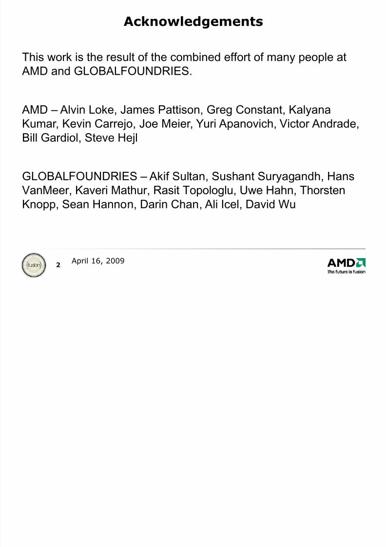
Acknowledgements
This work is the result of the combined effort of many people at AMD and GLOBALFOUNDRIES.
AMD – Alvin Loke, James Pattison, Greg Constant, KalyanaKumar, Kevin Carrejo, Joe Meier, Yuri Apanovich, Victor Andrade,Bill Gardiol, Steve Hejl
GLOBALFOUNDRIES – Akif Sultan, Sushant Suryagandh, HansVanMeer, Kaveri Mathur, Rasit Topologlu, Uwe Hahn, Thorsten
Knopp, Sean Hannon, Darin Chan, Ali Icel, David Wu
8/12/2019 STI Effects
http://slidepdf.com/reader/full/sti-effects 3/49
3April 16, 2009
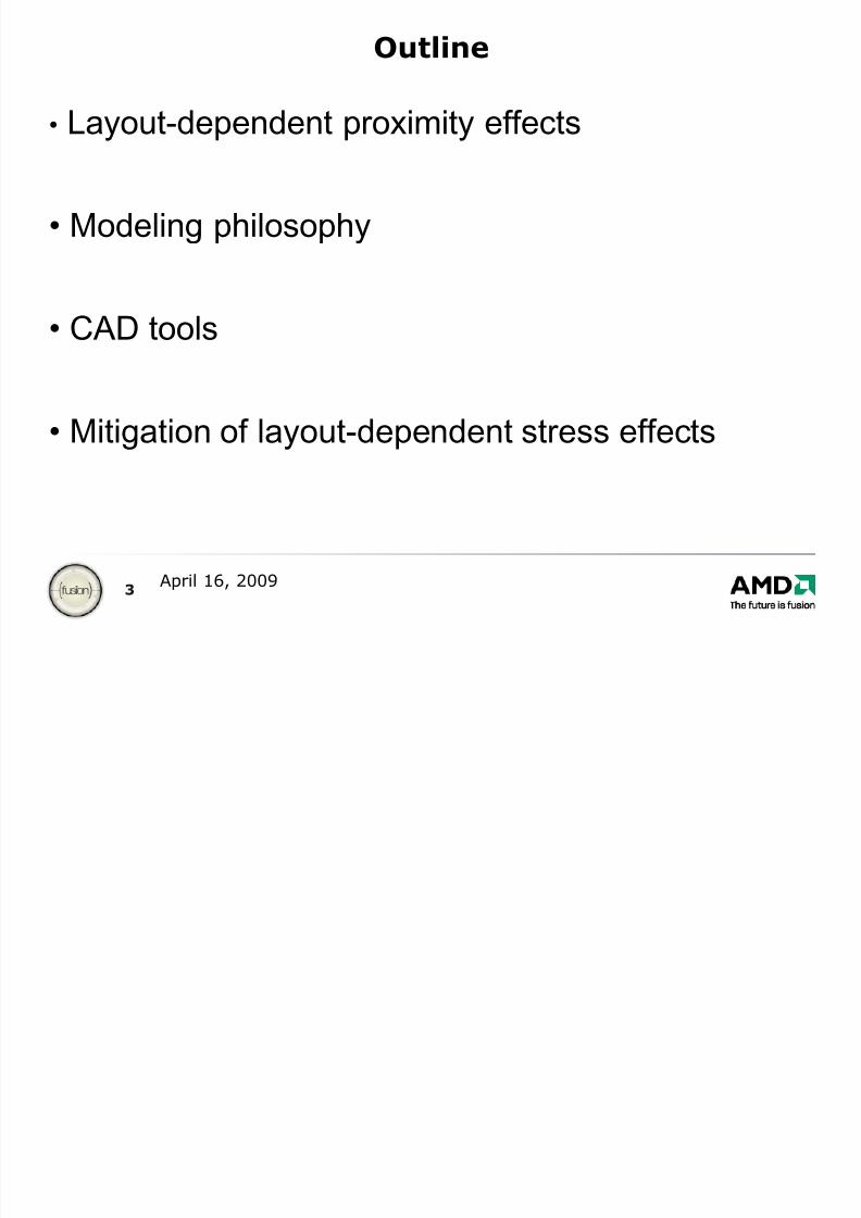
Outline
• Layout-dependent proximity effects
• Modeling philosophy
• CAD tools
• Mitigation of layout-dependent stress effects
8/12/2019 STI Effects
http://slidepdf.com/reader/full/sti-effects 4/49
4April 16, 2009
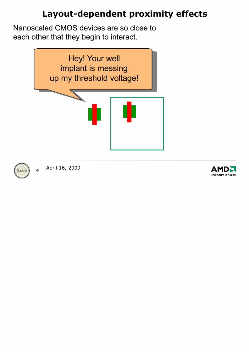
Nanoscaled CMOS devices are so close toeach other that they begin to interact.
Layout-dependent proximity effects
Hey! Your wellimplant is messing
up my threshold voltage!
8/12/2019 STI Effects
http://slidepdf.com/reader/full/sti-effects 5/49
8/12/2019 STI Effects
http://slidepdf.com/reader/full/sti-effects 6/49
6April 16, 2009
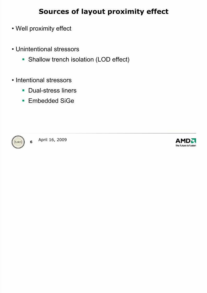
Sources of layout proximity effect
• Well proximity effect
• Unintentional stressors
Shallow trench isolation (LOD effect)
• Intentional stressors Dual-stress liners
Embedded SiGe
8/12/2019 STI Effects
http://slidepdf.com/reader/full/sti-effects 7/49
7April 16, 2009
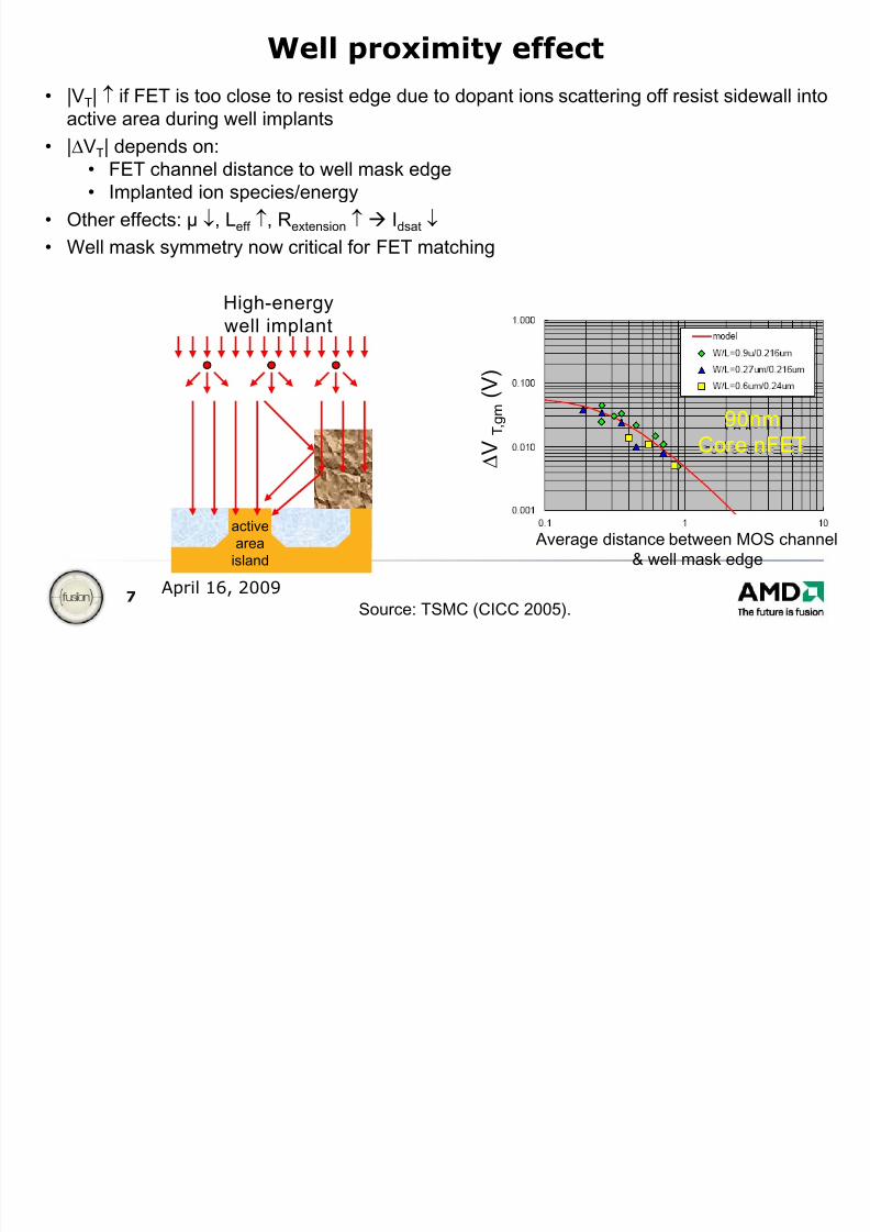
Well proximity effect
• |VT| ↑ if FET is too close to resist edge due to dopant ions scattering off resist sidewall into
active area during well implants
• |ΔVT| depends on:• FET channel distance to well mask edge• Implanted ion species/energy
• Other effects: µ ↓
, Leff ↑
, Rextension ↑
Idsat ↓
• Well mask symmetry now critical for FET matching
High-energy
well implant
Source: TSMC (CICC 2005).
90nm
Core nFET Δ V
T , g m
( V )
Average distance between MOS channel
& well mask edge
activearea
island
8/12/2019 STI Effects
http://slidepdf.com/reader/full/sti-effects 8/49
8April 16, 2009
A brief review of stress and strain…
8/12/2019 STI Effects
http://slidepdf.com/reader/full/sti-effects 9/49
9April 16, 2009
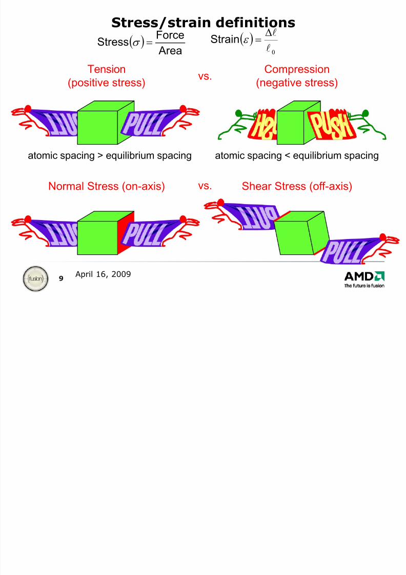
Stress/strain definitions
( ) Area
ForceStress =σ
atomic spacing > equilibrium spacing
Tension(positive stress)
Compression(negative stress)
atomic spacing < equilibrium spacing
Normal Stress (on-axis) Shear Stress (off-axis)
vs.
vs.
( )0
l
lΔ=ε Strain
8/12/2019 STI Effects
http://slidepdf.com/reader/full/sti-effects 10/49
10April 16, 2009
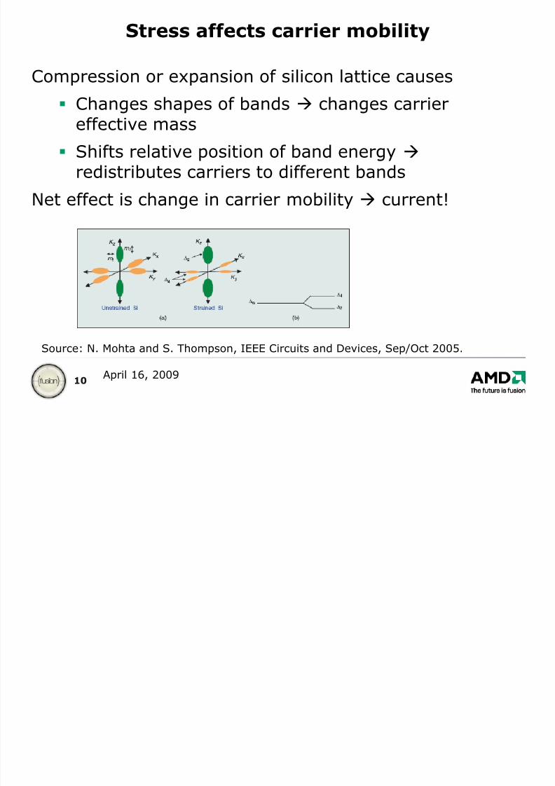
Stress affects carrier mobility
Compression or expansion of silicon lattice causes
Changes shapes of bands changes carriereffective mass
Shifts relative position of band energy
redistributes carriers to different bands
Net effect is change in carrier mobility current!
Source: N. Mohta and S. Thompson, IEEE Circuits and Devices, Sep/Oct 2005.
8/12/2019 STI Effects
http://slidepdf.com/reader/full/sti-effects 11/49
11April 16, 2009
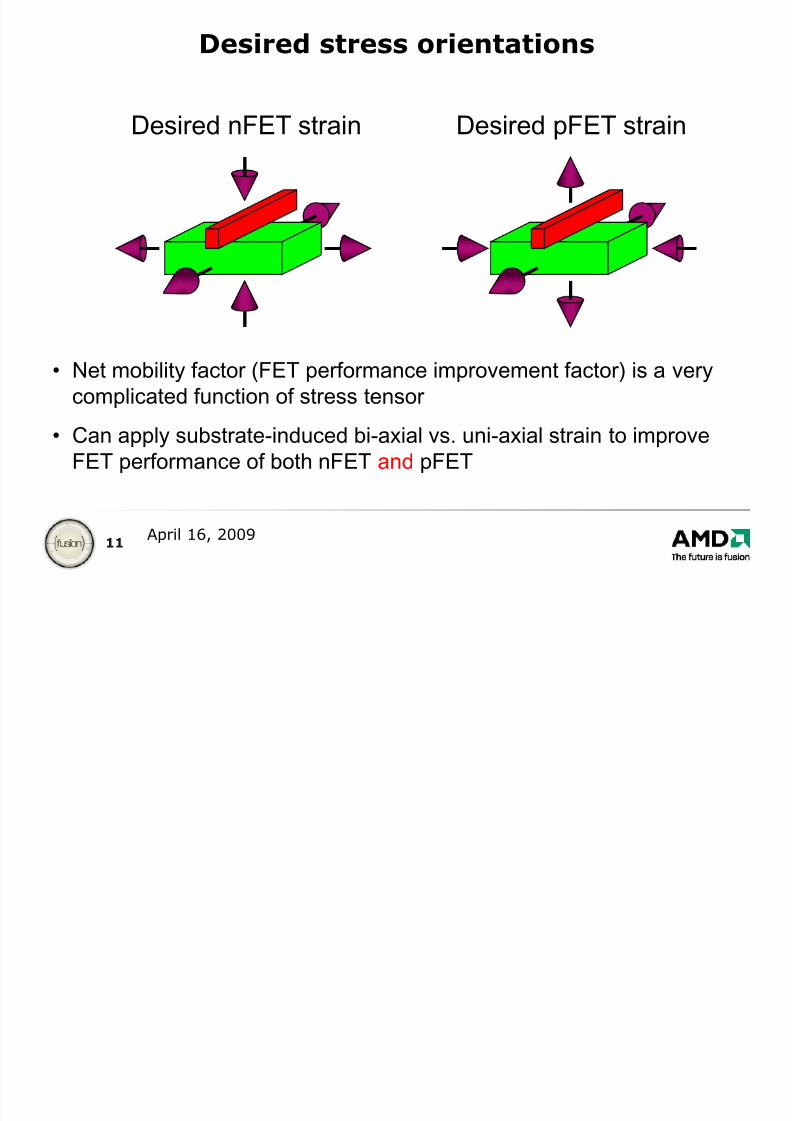
Desired stress orientations
• Net mobility factor (FET performance improvement factor) is a verycomplicated function of stress tensor
• Can apply substrate-induced bi-axial vs. uni-axial strain to improveFET performance of both nFET and pFET
Desired nFET strain Desired pFET strain
8/12/2019 STI Effects
http://slidepdf.com/reader/full/sti-effects 12/49
12April 16, 2009
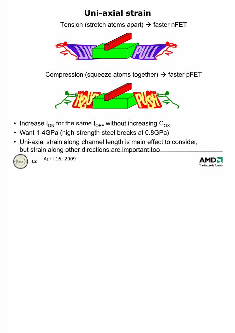
Uni-axial strain
Tension (stretch atoms apart) faster nFET
Compression (squeeze atoms together) faster pFET
• Increase ION for the same IOFF without increasing COX
• Want 1-4GPa (high-strength steel breaks at 0.8GPa)
• Uni-axial strain along channel length is main effect to consider,
but strain along other directions are important too
8/12/2019 STI Effects
http://slidepdf.com/reader/full/sti-effects 13/49
13April 16, 2009
Source of stress…
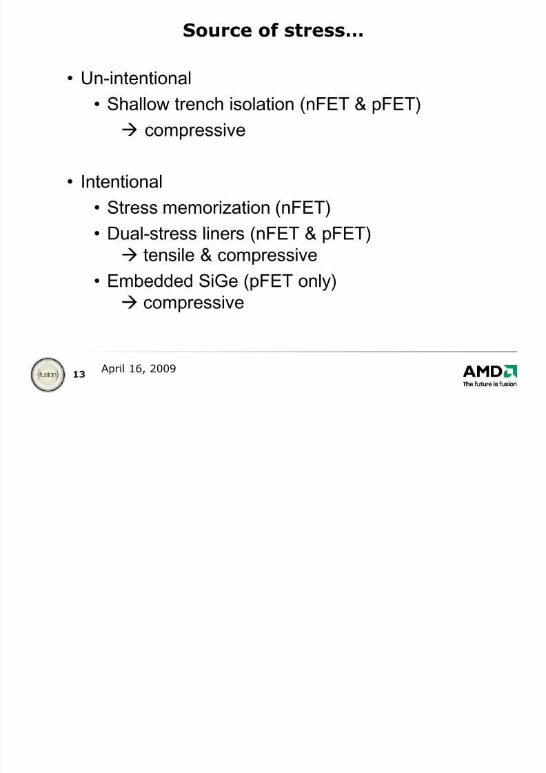
• Un-intentional
• Shallow trench isolation (nFET & pFET)
compressive
• Intentional
• Stress memorization (nFET)• Dual-stress liners (nFET & pFET)
tensile & compressive
• Embedded SiGe (pFET only) compressive
8/12/2019 STI Effects
http://slidepdf.com/reader/full/sti-effects 14/49
14April 16, 2009
Shallow trench isolation (LOD effect)
Source: Xi et al., UC Berkeley (2003).
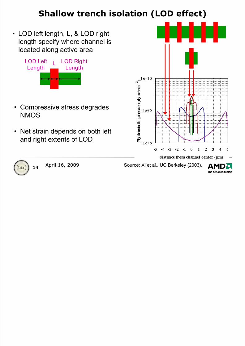
• LOD left length, L, & LOD rightlength specify where channel islocated along active area
LOD LeftLength L LOD RightLength
• Compressive stress degrades
NMOS
• Net strain depends on both leftand right extents of LOD
8/12/2019 STI Effects
http://slidepdf.com/reader/full/sti-effects 15/49
15April 16, 2009
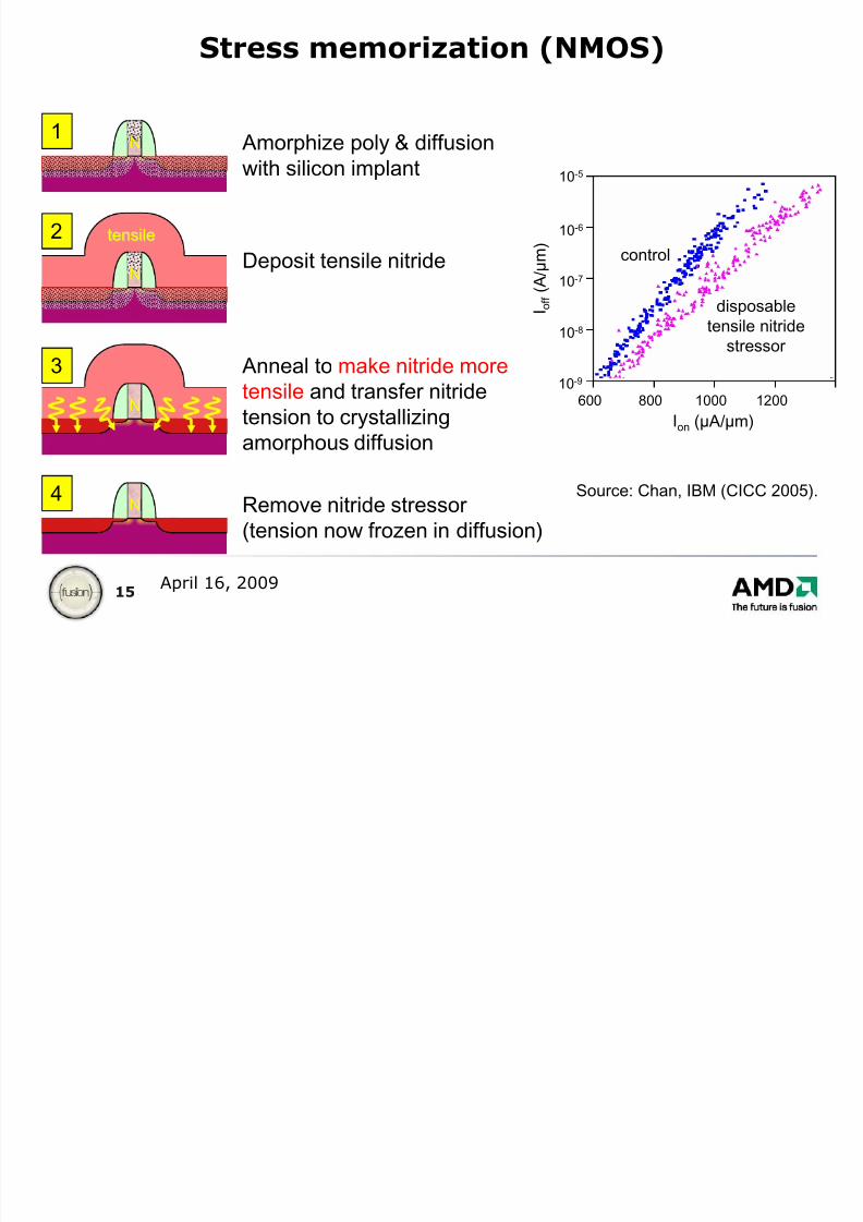
Stress memorization (NMOS)
Source: Chan, IBM (CICC 2005).
Ion (µA/µm)
I o f f
( A / µ m )
600 800 1000 120010-9
10-8
10-7
10-6
10-5
control
disposabletensile nitride
stressor
tensile
N
N
Amorphize poly & diffusionwith silicon implant
Deposit tensile nitride
N
Anneal to make nitride more
tensile and transfer nitridetension to crystallizing
amorphous diffusion
N Remove nitride stressor(tension now frozen in diffusion)
1
2
3
4
8/12/2019 STI Effects
http://slidepdf.com/reader/full/sti-effects 16/49
16April 16, 2009
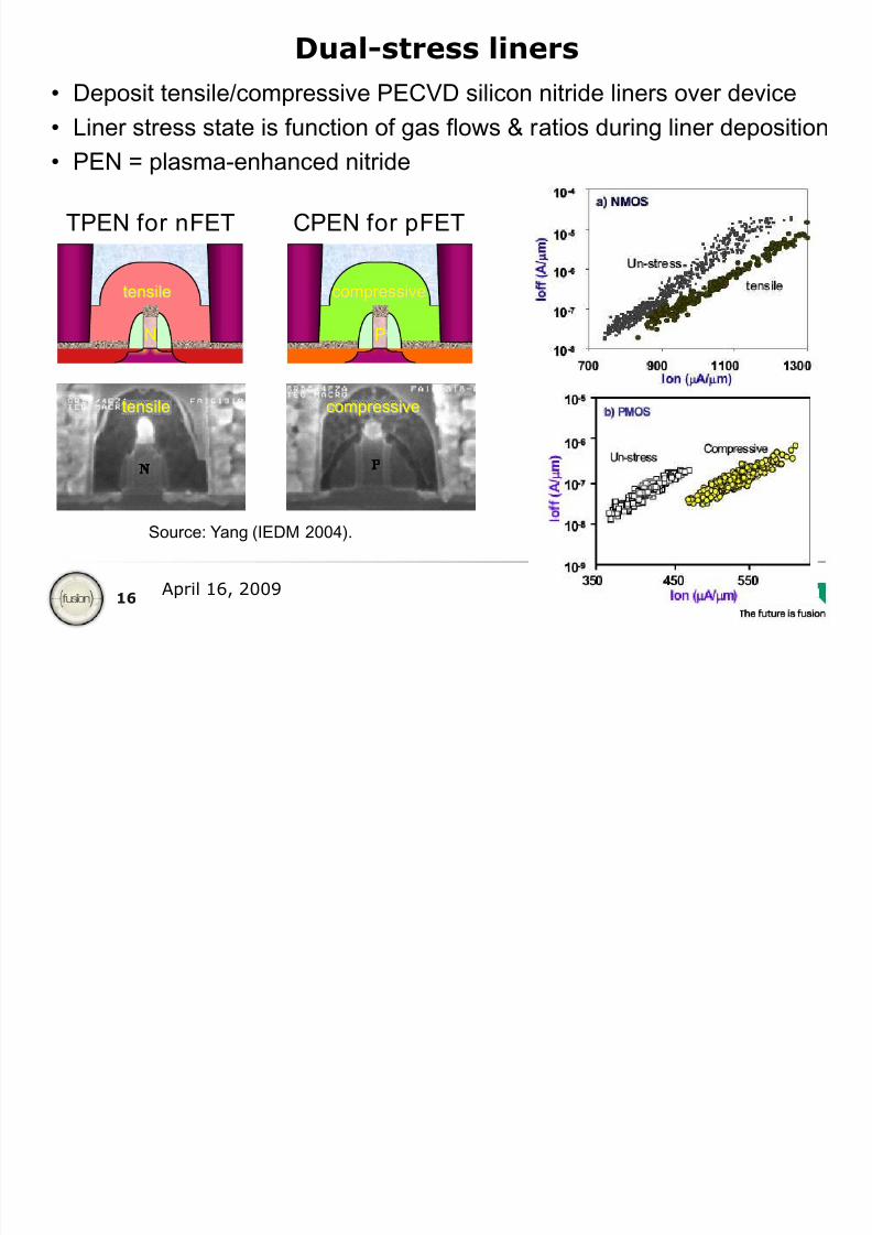
Dual-stress liners
• Deposit tensile/compressive PECVD silicon nitride liners over device
• Liner stress state is function of gas flows & ratios during liner deposition
• PEN = plasma-enhanced nitride
Source: Yang (IEDM 2004).
TPEN for nFET CPEN for pFET
tensile compressive
tensile
N P
compressive
8/12/2019 STI Effects
http://slidepdf.com/reader/full/sti-effects 17/49
17April 16, 2009
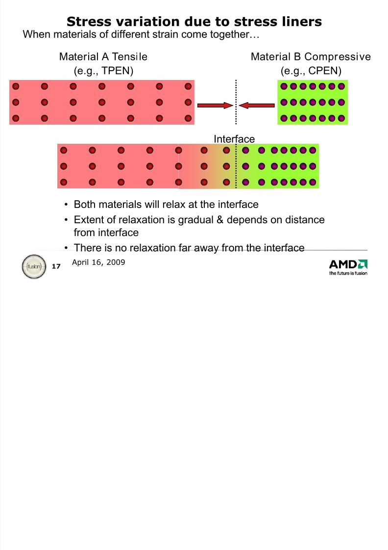
Stress variation due to stress linersWhen materials of different strain come together…
Material A Tensi le
(e.g., TPEN)
Material B Compressive
(e.g., CPEN)
• Both materials will relax at the interface• Extent of relaxation is gradual & depends on distance
from interface
• There is no relaxation far away from the interface
Interface
8/12/2019 STI Effects
http://slidepdf.com/reader/full/sti-effects 18/49
18April 16, 2009
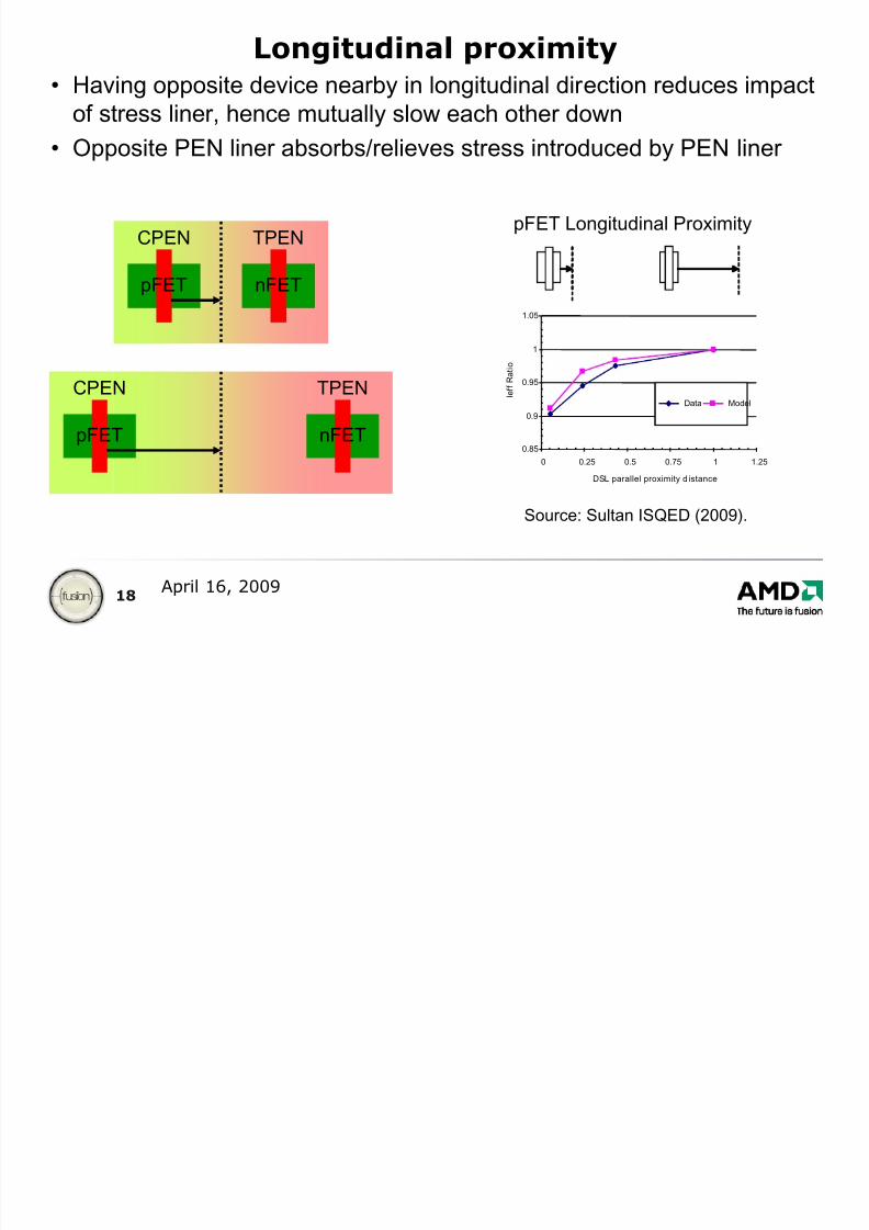
Longitudinal proximity
• Having opposite device nearby in longitudinal direction reduces impact
of stress liner, hence mutually slow each other down• Opposite PEN liner absorbs/relieves stress introduced by PEN liner
CPEN TPEN
pFET nFET
CPEN TPEN
pFET nFET
pFET Longitudinal Proximity
Source: Sultan ISQED (2009).
0.85
0.9
0.95
1
1.05
0 0.25 0.5 0.75 1 1.25
DSL parallel proximity d istance
I e f f R a t i o
Data Model
8/12/2019 STI Effects
http://slidepdf.com/reader/full/sti-effects 19/49
19April 16, 2009
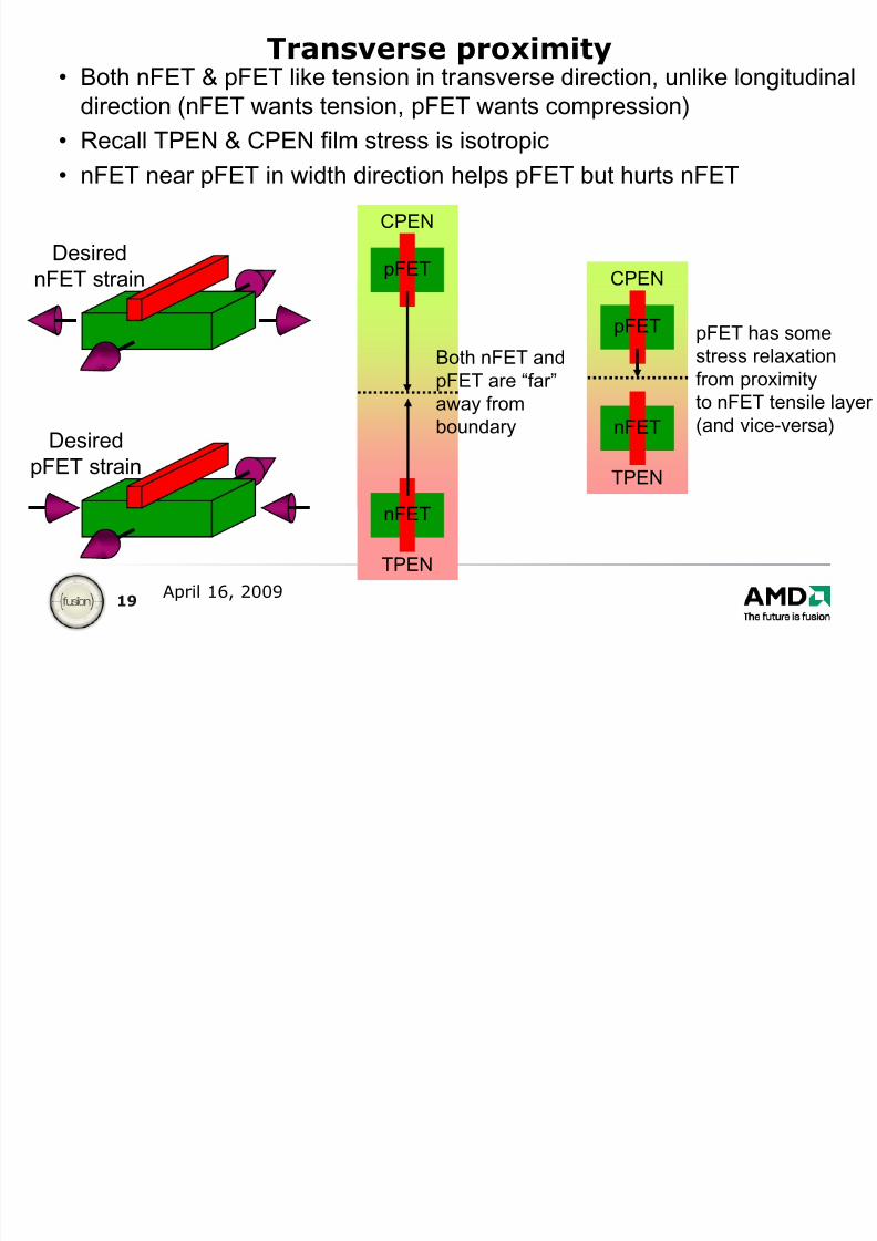
Transverse proximity• Both nFET & pFET like tension in transverse direction, unlike longitudinal
direction (nFET wants tension, pFET wants compression)• Recall TPEN & CPEN film stress is isotropic
• nFET near pFET in width direction helps pFET but hurts nFET
DesirednFET strain
DesiredpFET strain
CPEN
TPEN
pFET
nFET
CPEN
TPEN
pFET
nFET
Both nFET andpFET are “far”away fromboundary
pFET has somestress relaxationfrom proximityto nFET tensile layer (and vice-versa)
8/12/2019 STI Effects
http://slidepdf.com/reader/full/sti-effects 20/49
20April 16, 2009
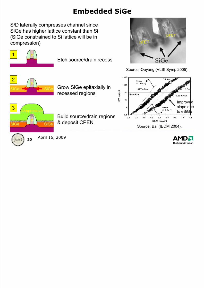
Embedded SiGe
3 compressive
P
P
Etch source/drain recess
Grow SiGe epitaxially inrecessed regions
2
SiGe SiGe
PSiGe SiGe
S/D laterally compresses channel sinceSiGe has higher lattice constant than Si(SiGe constrained to Si lattice will be incompression)
pFET
pFET
1
Source: Bai (IEDM 2004).
Source: Ouyang (VLSI Symp 2005).
Build source/drain regions& deposit CPEN
Improved
slope dueto eSiGe
8/12/2019 STI Effects
http://slidepdf.com/reader/full/sti-effects 21/49
21April 16, 2009
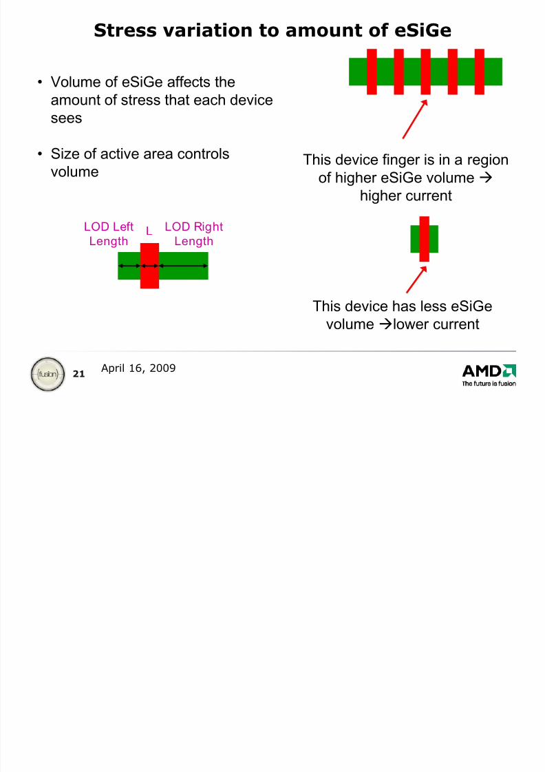
Stress variation to amount of eSiGe
• Volume of eSiGe affects theamount of stress that each devicesees
• Size of active area controlsvolume
LOD Left
LengthL LOD Right
Length
This device finger is in a regionof higher eSiGe volume
higher current
This device has less eSiGevolume lower current

8/12/2019 STI Effects
http://slidepdf.com/reader/full/sti-effects 22/49
22April 16, 2009
Modeling philosophy
Two scenarios:
PhD thesis approach – model everything possible
“Good enough” approach – model the most importanteffects and try to get those “right”
8/12/2019 STI Effects
http://slidepdf.com/reader/full/sti-effects 23/49
23April 16, 2009
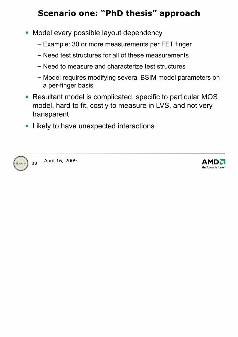
Scenario one: “PhD thesis” approach
Model every possible layout dependency
– Example: 30 or more measurements per FET finger
– Need test structures for all of these measurements
– Need to measure and characterize test structures
– Model requires modifying several BSIM model parameters ona per-finger basis
Resultant model is complicated, specific to particular MOSmodel, hard to fit, costly to measure in LVS, and not verytransparent
Likely to have unexpected interactions
8/12/2019 STI Effects
http://slidepdf.com/reader/full/sti-effects 24/49
24April 16, 2009
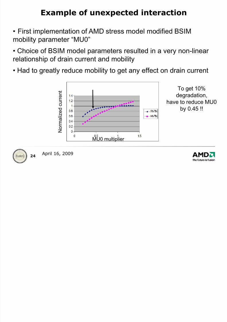
Example of unexpected interaction
• First implementation of AMD stress model modified BSIMmobility parameter “MU0”
• Choice of BSIM model parameters resulted in a very non-linear
relationship of drain current and mobility• Had to greatly reduce mobility to get any effect on drain current
MU0 multiplier
N o r m a
l i z e d c u r r e n t To get 10%
degradation,have to reduce MU0
by 0.45 !!
8/12/2019 STI Effects
http://slidepdf.com/reader/full/sti-effects 25/49
25April 16, 2009
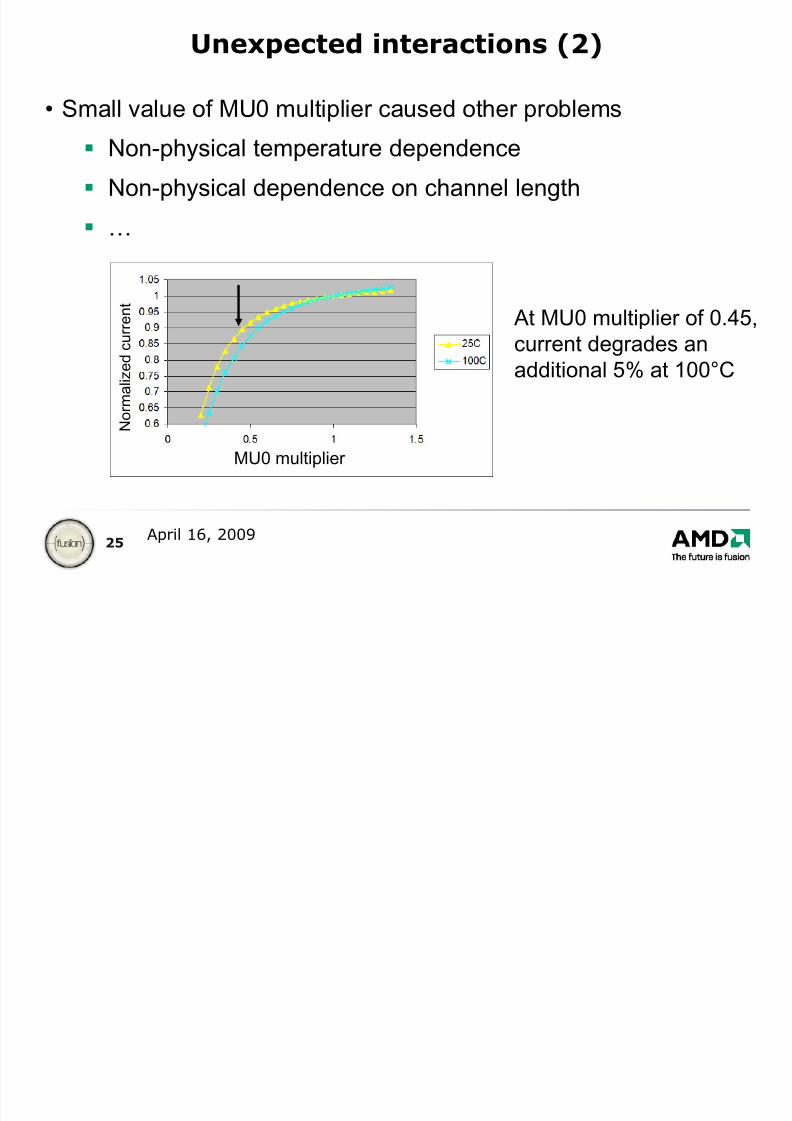
Unexpected interactions (2)
• Small value of MU0 multiplier caused other problems
Non-physical temperature dependence
Non-physical dependence on channel length
…
MU0 multiplier
N o r m a l i z e d c u r r e n
t
At MU0 multiplier of 0.45,current degrades anadditional 5% at 100°C
8/12/2019 STI Effects
http://slidepdf.com/reader/full/sti-effects 26/49
26April 16, 2009
Scenario two: “Good enough” approach
Model only most important effects
Use phenomenological approach – we measure changes indrain current and threshold on test structures
Use hooks in circuit simulator to adjust drain current andthreshold directly on per-instance basis
Transparent - designer sees exactly what is happening to
device
Easy to debug, no interaction with choice of transistor modelparameters
Downside - not every physical effect can be modeled(maybe a good thing?)
8/12/2019 STI Effects
http://slidepdf.com/reader/full/sti-effects 27/49
27April 16, 2009
“It’s only a model”
Monty Python and the HolyGrail
CAD
Implementation
8/12/2019 STI Effects
http://slidepdf.com/reader/full/sti-effects 28/49
28April 16, 2009
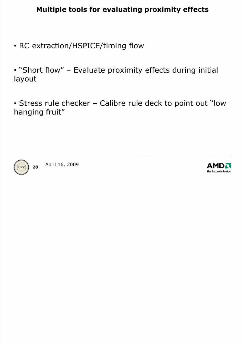
Multiple tools for evaluating proximity effects
• RC extraction/HSPICE/timing flow
• “Short flow” – Evaluate proximity effects during initiallayout
• Stress rule checker – Calibre rule deck to point out “lowhanging fruit”
8/12/2019 STI Effects
http://slidepdf.com/reader/full/sti-effects 29/49
29April 16, 2009
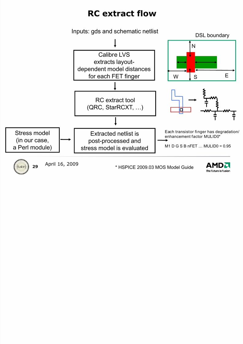
RC extract flow
Inputs: gds and schematic netlist
Calibre LVS
extracts layout-dependent model distancesfor each FET finger
RC extract tool(QRC, StarRCXT, …)
Extracted netlist ispost-processed and
stress model is evaluated
Stress model(in our case,
a Perl module)
Each transistor finger has degradation/
enhancement factor MULID0*
M1 D G S B nFET … MULID0 = 0.95
* HSPICE 2009.03 MOS Model Guide
DSL boundary
N
S EW
8/12/2019 STI Effects
http://slidepdf.com/reader/full/sti-effects 30/49
30April 16, 2009
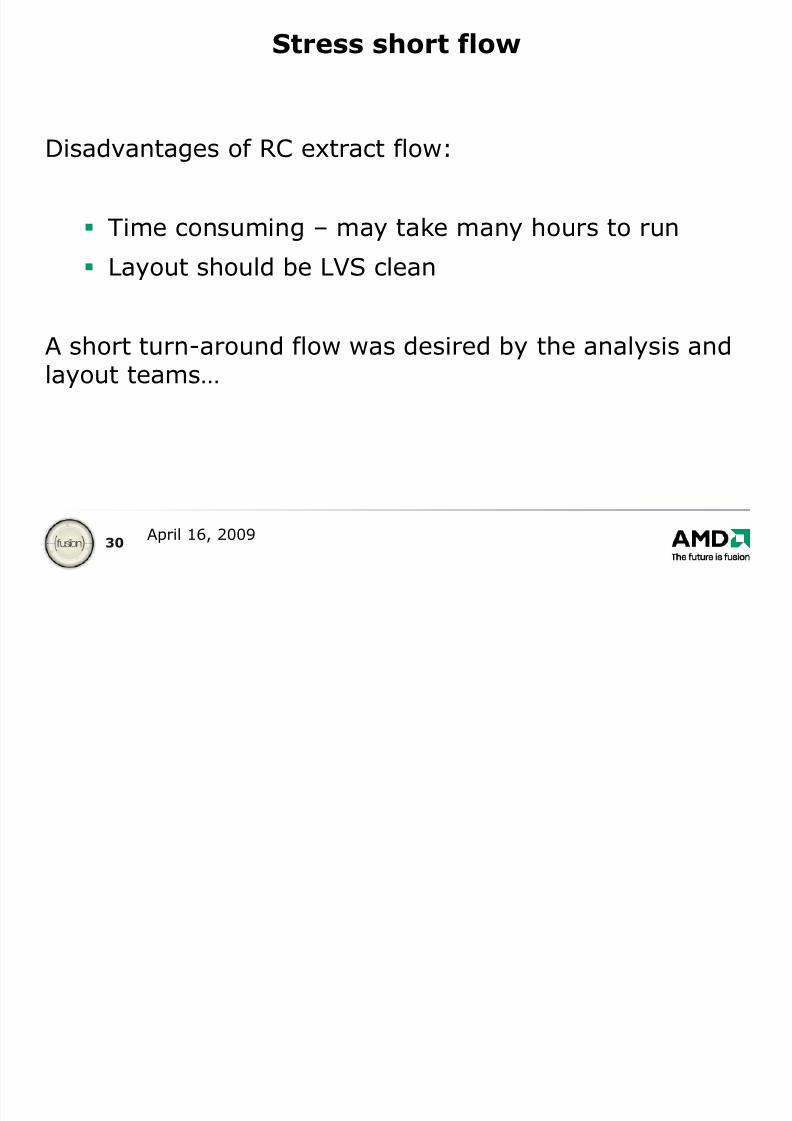
Stress short flow
Disadvantages of RC extract flow:
Time consuming – may take many hours to run
Layout should be LVS clean
A short turn-around flow was desired by the analysis andlayout teams…
8/12/2019 STI Effects
http://slidepdf.com/reader/full/sti-effects 31/49
31April 16, 2009
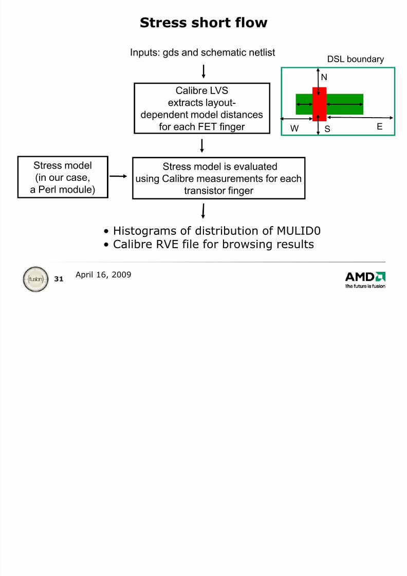
Stress short flow
Inputs: gds and schematic netlist
Calibre LVS
extracts layout-dependent model distancesfor each FET finger
Stress model is evaluatedusing Calibre measurements for each
transistor finger
Stress model(in our case,
a Perl module)
• Histograms of distribution of MULID0• Calibre RVE file for browsing results
DSL boundary
N
S EW
8/12/2019 STI Effects
http://slidepdf.com/reader/full/sti-effects 32/49
32April 16, 2009
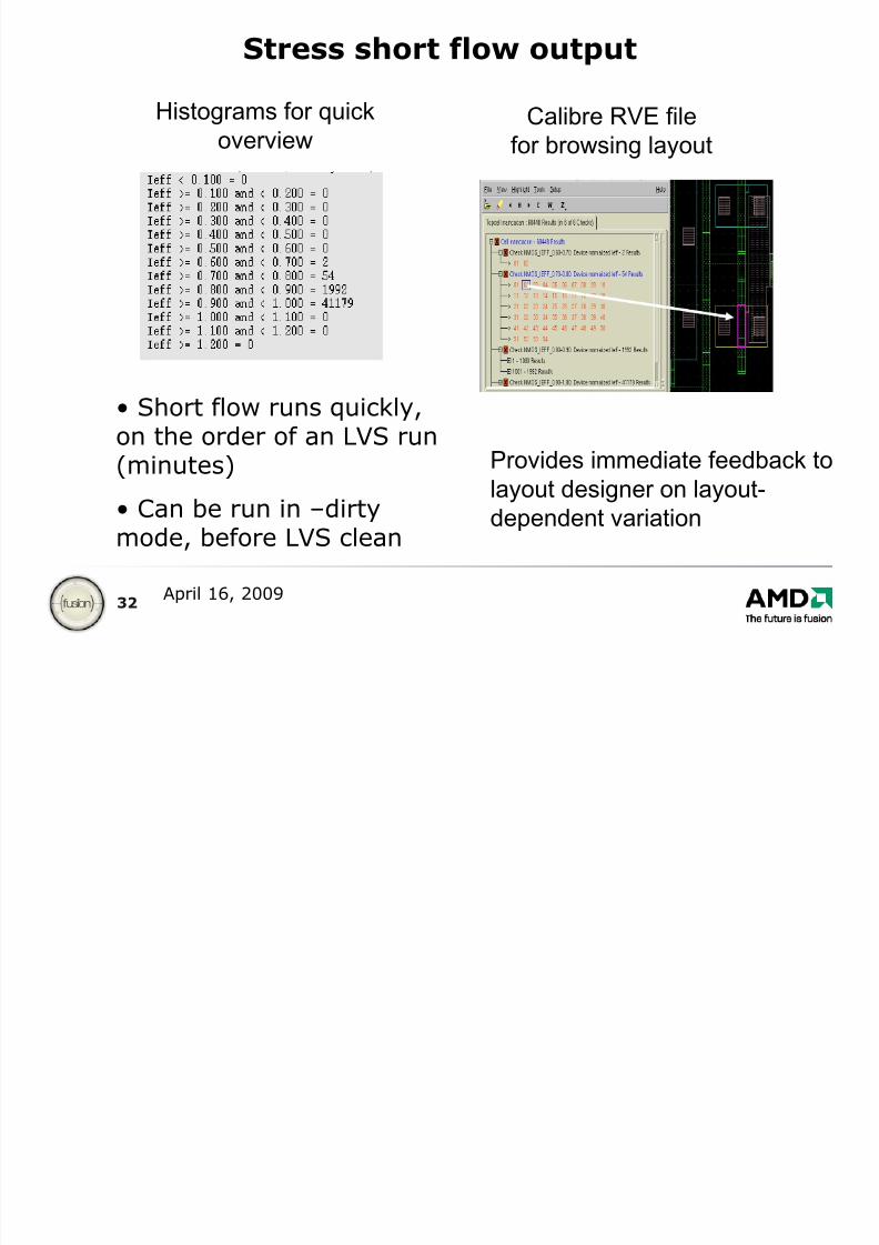
Stress short flow output
Histograms for quickoverview Calibre RVE filefor browsing layout
• Short flow runs quickly,on the order of an LVS run
(minutes)
• Can be run in –dirtymode, before LVS clean
Provides immediate feedback tolayout designer on layout-dependent variation
8/12/2019 STI Effects
http://slidepdf.com/reader/full/sti-effects 33/49
33April 16, 2009
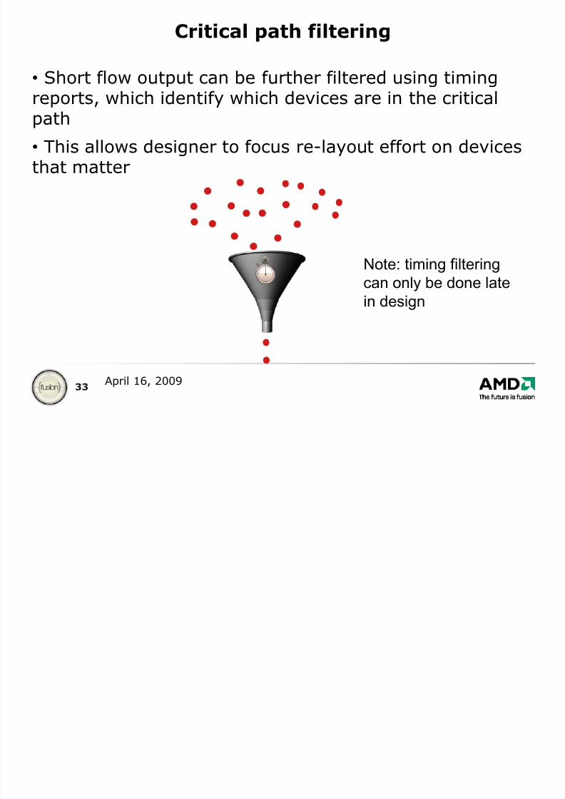
Critical path filtering
• Short flow output can be further filtered using timingreports, which identify which devices are in the criticalpath
• This allows designer to focus re-layout effort on devicesthat matter
Note: timing filteringcan only be done late
in design
8/12/2019 STI Effects
http://slidepdf.com/reader/full/sti-effects 34/49
34April 16, 2009
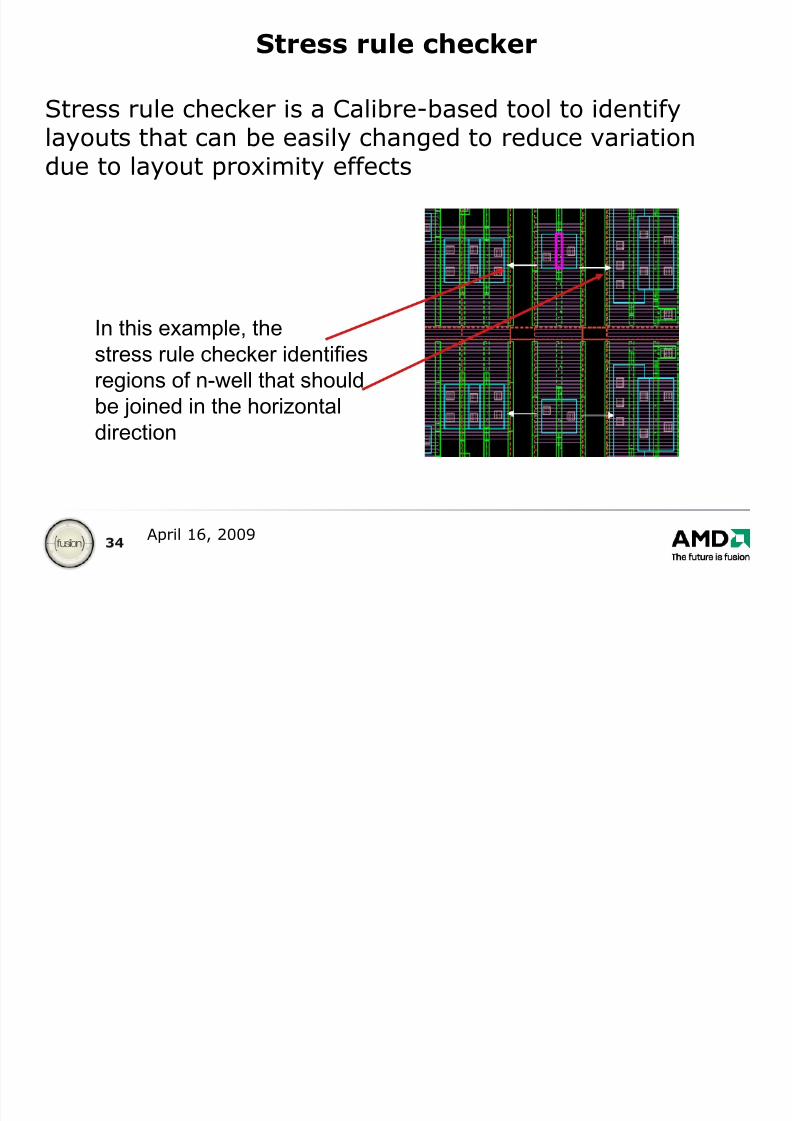
Stress rule checker
Stress rule checker is a Calibre-based tool to identifylayouts that can be easily changed to reduce variationdue to layout proximity effects
In this example, thestress rule checker identifiesregions of n-well that should
be joined in the horizontaldirection
8/12/2019 STI Effects
http://slidepdf.com/reader/full/sti-effects 35/49
35April 16, 2009
Guidelines for mitigation of
layout-dependent
effects
8/12/2019 STI Effects
http://slidepdf.com/reader/full/sti-effects 36/49
36April 16, 2009
Mitigation guidelines come in two flavors:
Minimize variation from base SPICE model
Minimize variation between devices that need to bematched
We’ll focus here on device matching…
8/12/2019 STI Effects
http://slidepdf.com/reader/full/sti-effects 37/49
37April 16, 2009
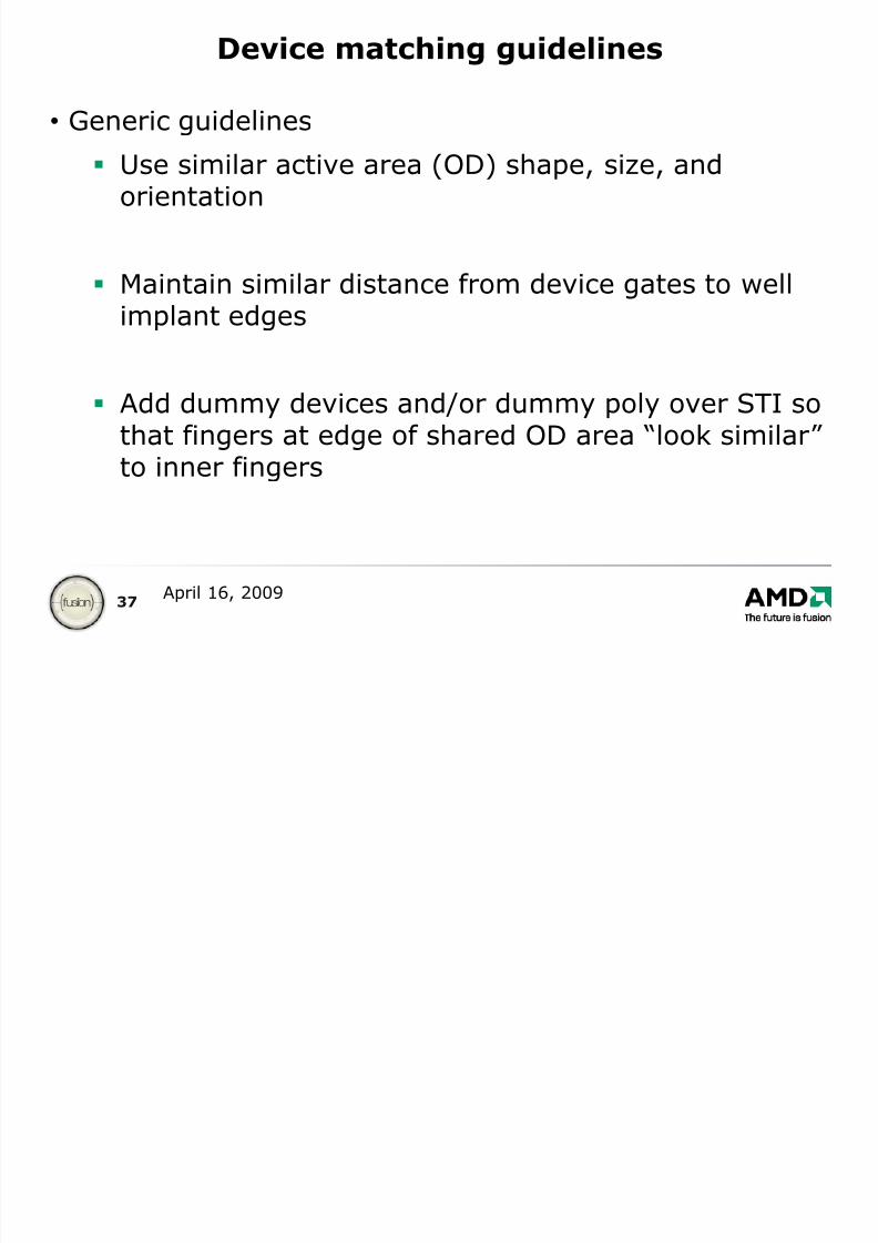
Device matching guidelines
• Generic guidelines
Use similar active area (OD) shape, size, andorientation
Maintain similar distance from device gates to wellimplant edges
Add dummy devices and/or dummy poly over STI sothat fingers at edge of shared OD area “look similar”
to inner fingers
8/12/2019 STI Effects
http://slidepdf.com/reader/full/sti-effects 38/49
38April 16, 2009
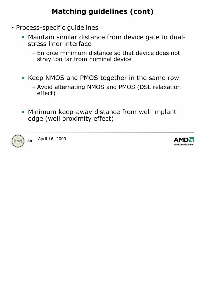
Matching guidelines (cont)
• Process-specific guidelines Maintain similar distance from device gate to dual-
stress liner interface
– Enforce minimum distance so that device does notstray too far from nominal device
Keep NMOS and PMOS together in the same row
– Avoid alternating NMOS and PMOS (DSL relaxationeffect)
Minimum keep-away distance from well implantedge (well proximity effect)
8/12/2019 STI Effects
http://slidepdf.com/reader/full/sti-effects 39/49
39April 16, 2009
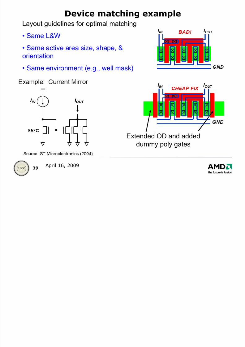
Device matching exampleLayout guidelines for optimal matching
• Same L&W
• Same active area size, shape, &orientation
• Same environment (e.g., well mask)
Extended OD and addeddummy poly gates
8/12/2019 STI Effects
http://slidepdf.com/reader/full/sti-effects 40/49
40April 16, 2009
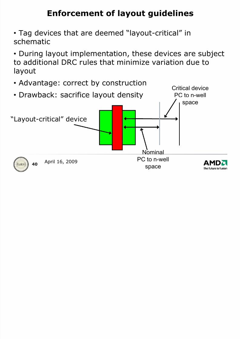
Enforcement of layout guidelines
• Tag devices that are deemed “layout-critical” inschematic
• During layout implementation, these devices are subject
to additional DRC rules that minimize variation due tolayout
• Advantage: correct by construction
• Drawback: sacrifice layout density
“Layout-critical” device
NominalPC to n-well
space
Critical device
PC to n-wellspace
8/12/2019 STI Effects
http://slidepdf.com/reader/full/sti-effects 41/49
8/12/2019 STI Effects
http://slidepdf.com/reader/full/sti-effects 42/49
42April 16, 2009
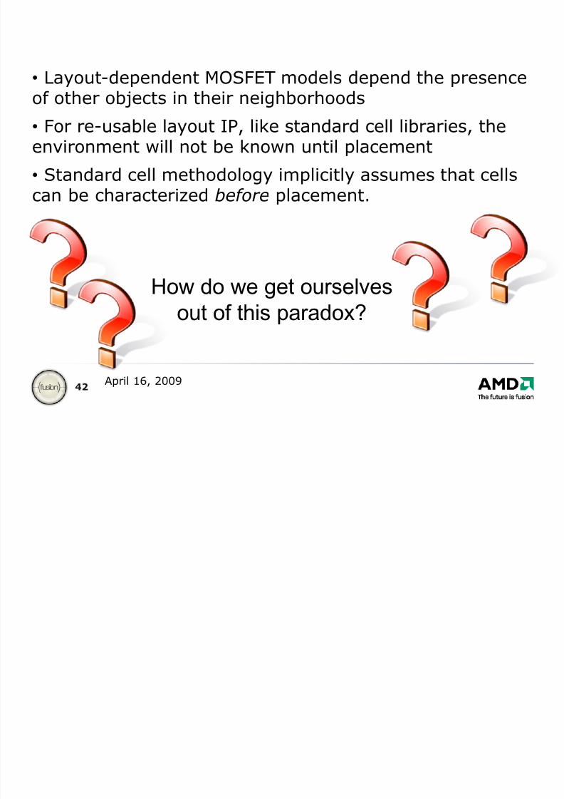
• Layout-dependent MOSFET models depend the presenceof other objects in their neighborhoods
• For re-usable layout IP, like standard cell libraries, the
environment will not be known until placement• Standard cell methodology implicitly assumes that cellscan be characterized before placement.
How do we get ourselvesout of this paradox?
8/12/2019 STI Effects
http://slidepdf.com/reader/full/sti-effects 43/49
43April 16, 2009
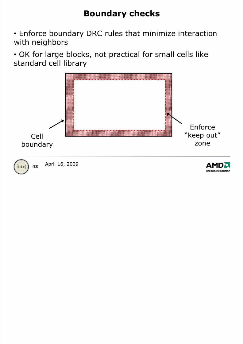
Boundary checks
• Enforce boundary DRC rules that minimize interactionwith neighbors
• OK for large blocks, not practical for small cells like
standard cell library
Cellboundary
Enforce “keep out”
zone
8/12/2019 STI Effects
http://slidepdf.com/reader/full/sti-effects 44/49
44April 16, 2009
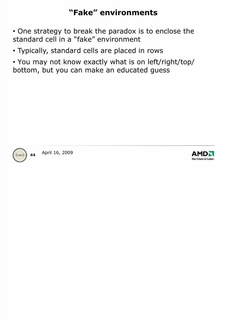
“Fake” environments
• One strategy to break the paradox is to enclose thestandard cell in a “fake” environment
• Typically, standard cells are placed in rows
• You may not know exactly what is on left/right/top/bottom, but you can make an educated guess
8/12/2019 STI Effects
http://slidepdf.com/reader/full/sti-effects 45/49
45April 16, 2009
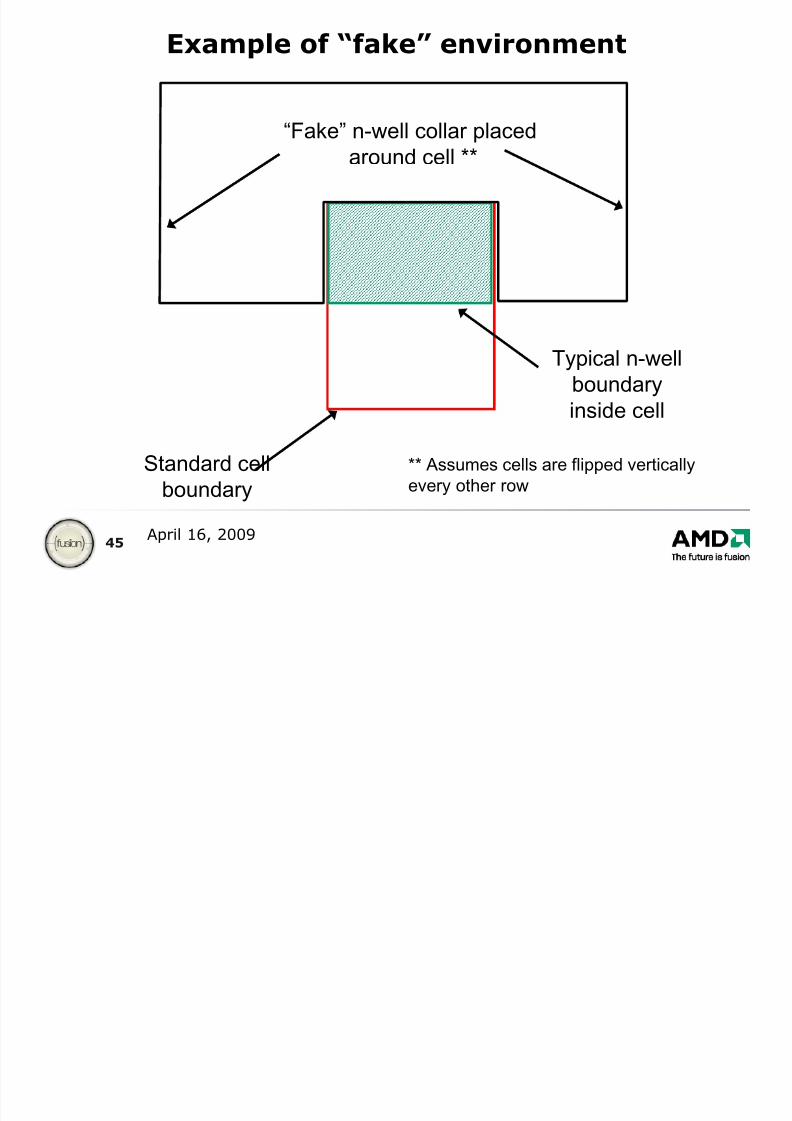
Example of “fake” environment
Standard cellboundary
Typical n-wellboundary
inside cell
“Fake” n-well collar placedaround cell **
** Assumes cells are flipped verticallyevery other row
8/12/2019 STI Effects
http://slidepdf.com/reader/full/sti-effects 46/49
46April 16, 2009
Exhaustive simulation
• CAD vendors provide tools that extract the cell with allpossible neighbor cells to quantify variation (example:Cadence LEA tool)
• Cell variation information is useful feedback for stdcelldesign team, but is it useful for design flow?
8/12/2019 STI Effects
http://slidepdf.com/reader/full/sti-effects 47/49
47April 16, 2009
A p o s t e r i o r i checks
• Run stress_short_flow after placement to look for outlierdevices
• The flow is efficient – cost is on the order of an LVS run
• But this is very late in the flow to find these issues
8/12/2019 STI Effects
http://slidepdf.com/reader/full/sti-effects 48/49
48April 16, 2009
Summary
• Described sources of device variation due to layout
• Modeling methodology
Keep things simple
A model that can be evaluated outside of a circuitsimulator is really handy
• CAD tool implementation
Provide quick feedback tools for the layout team
Interface to detailed analysis tools (e.g., circuitsimulation)
• Layout guidelines for critical devices
8/12/2019 STI Effects
http://slidepdf.com/reader/full/sti-effects 49/49
49April 16, 2009
Trademark Attribution
AMD, the AMD Arrow logo and combinations thereof are trademarks of Advanced Micro Devices,
Inc. in the United States and/or other jurisdictions. Other names used in this presentation are foridentification purposes only and may be trademarks of their respective owners.
©2009 Advanced Micro Devices, Inc. All rights reserved.