
SHIELD SECURITY - BALUNS PASIVOS, TODAS LAS MARCAS Y MODELOS

1
State of the Art for Differential Circuits and Baluns in Wireless
Communications Transceivers; A New Wideband Active Balun in SiGe-BiCMOS Technology
Balwant Godara Alain Fabre
e-mail: [email protected] e-mail: [email protected] Laboratoire IXL, Université Bordeaux 1, Talence, France
Key words: Active Baluns, Current Conveyors, Differential Analog Circuits, S-Parameters, SiGe BiCMOS
ABSTRACT
The aim of this paper is three-fold : firstly, to provide a comprehensive overview of the use of differential circuits for analog signal processing in wireless transceivers; secondly, to describe in detail the conversion of single-ended signals to differential : corresponding theory of such devices, their characterisation, various methods of implementation and comparative analyses of their performance; and, finally, to propose a new solution for wideband baluns using active elements. This novel solution is based on the current conveyor; it has been modelled using the transistors parameters of a 0.35µm SiGe BiCMOS technology. The salient features of the new implementation are : (a) stable 50Ω input-port impedance and easily controllable output impedance (50Ω/75Ω/100Ω); (b) stable matching between the differential output ports : within 1dB(3dB) amplitude and 10°(20°) phase balance up-to 2GHz(3GHz); (c) good signal quality : output signal harmonic distortion lower than 1% for input signals up-to 50mV; (d) excellent S-parameter performance (0-3GHz) : return losses lower than –10dB, reverse signal rejection better than 20dB, more than 25dB isolation between the two output ports, and 42dB common-mode rejection; and (d) stable performance over a 100°C operating temperature range. This performance advances the state of the art for single-ended to differential conversion circuits (evinced upon detailed comparisons to existent baluns).
I. INTRODUCTION Based on the type of signal, active networks can be classified into 3 different categories: single-ended or unbalanced (hereafter abbreviated as SE), differential and fully balanced (FB). The same nomenclature applies to systems, according to the kind of signal they process. The input of any system generally contains a common-mode (CM) component and a differential-mode (DM) component, the former representing the undesired signal (to be suppressed) and the latter the information to be treated [1].
Single-Ended signals are defined with the ground plane as reference; the CM and DM components are treated equally; and parasitic CM components accumulate at the output. Consequently, systems which treat such signals suffer from limited dynamic range. In a differential system the output is defined as the difference between two terminals, neither of which is at ground potential; the differential output is here independent of the input CM signal; engendering an improved performance. However, the output swing of the DM signal is limited because the undesired CM part of the inputs experiences the same gain as the differential signal and is still transferred to the output. Finally, a FB system is a differential system with a constant CM output signal; this additional property enhances the achievable dynamic range. In recent years, the use of differential, pseudo-differential and FB signals has increased at such a rate that there are reasonable claims that “differential signals are the wave of the future for high-speed, high-volume data transmissions” [2].
PLAN OF THE PAPER
This article purports to first provide a glimpse of the state of the art in single-ended to differential converters for wireless communications systems and then to advance this art. Its organisation is as follows. Section II, an extended prelude, discusses the deployment of differential signals (and corresponding processing circuits) in present-day wireless transceivers : examples of differential topologies, their inherent advantages and limitations, layout issues, a basic analysis using SE half-circuits, and, finally, the different ways of measuring the characteristics of differential devices. Section III deals with single-ended to differential conversion. Baluns are first defined and their major applications enumerated; the theory and performance parameters are then presented; the various methods used to implement balun functions are thereafter detailed and compared (transformers, waveguides, transmission lines, LC networks and, rarest of all, active circuits). The next section presents a new proposal for realising active baluns, with the current conveyor (CCII) at its core.

2
Current conveyors are first introduced, followed by the principle of converting SE signals to differential using CCCIIs, and the design methodology is explained. The simulated performance of this new realisation is then summarized : DC, AC, transient and noise responses, S-parameter analyses and temperature stability. Finally, this performance is scrutinised in light of comparisons to other balun structures taken from published literature and industry datasheets. The article ends with some discussions and concluding remarks.
II. THE DIFFERENTIAL WORLD
FUNDAMENTAL ASSUMPTION
The fundamental assumption made for analysis of differential circuits is perfect symmetry. (The differential circuit is considered to be two perfectly identical SE counterparts connected in parallel.) In reality, however, symmetry is disturbed; and the degree of dissymmetry is critical to the functioning of differential circuits [3].
EXAMPLES OF DIFFERENTIAL TOPOLOGIES Balanced circuits have historically been used in low frequency analog circuitry and digital devices, and much less so in RF and microwave applications. Given below are some examples of differential circuits as they are found in today’s transceivers. Emphasis is here laid on radio- and microwave frequencies.
Elementary building blocks Instances of fully differential analog building blocks abound. These are then used to realise functions which are themselves differential. Some of them are :
• Special differential pairs for neural networks [4]; • Wide-range differential difference amplifiers [5]; • Differential current conveyors (the advantage is
that both positive and negative CCII types have the same realization) [1], [6]; and
• Active loads for adaptive filtering [7].
Individual Components Several RF components also use differential structures. These are fabricated in all the leading technologies (silicon-based, GaAs, etc.), CMOS being the implementation choice at RF. Some of the commonest :
• Low Noise Amplifiers (LNA) : for 900MHz applications [8],[9], 2.1GHz WCDMA [10], 5GHz WLAN [11];
• Power Amplifiers (PA) : for frequencies from 700MHz [12] through 2GHz [13] to 5GHz [14];
• Variable Gain Amplifiers (VGA) : in bipolar [15] and CMOS for video applications [16];
• Other amplifiers : general-purpose wideband amplifiers in bipolar [17], wideband distributed
amplifier [18], buffer amplifiers [19]; IF amplifier [20]; high-power GaAs FET amplifiers for cellular base stations [21]; trans-impedance amplifier in InP–InGaAs SHBT for 40Gbps SONET [22], operational trans-conductance amplifier with read-out rates up to 10-Mpixels/s for image sensors [23];
• Double-balanced I/Q Mixers : in CMOS for 2.1GHz WCDMA [10], in InGaP/GaAs HBT, for 20–40GHz [24]; and
• Other circuits : 2.5V 40Gbps decision circuit [25], Current Mode Comparator [26].
Sub-systems
In an increasing trend, differential sub-systems are being developed :
• RF Front-ends, with LNA and mixer (fig. 1) : bipolar front-end for multi-standard receivers [27], BiCMOS front-end for dual-mode WCDMA/GSM [28], BiCMOS 5-6GHz WLAN front-end [29]; and
LNA
Mixer I
Mixer Q
IN
OUT I
OUT Q
Figure 1 : Typical Differential RF Front-end
• Up-converters, with I/Q modulator, IF VGA and double-balanced mixer [30], [31].
Receivers/Transmitters
Most communications transceiver architectures today utilise a combination of SE and differential components. But recently, some entirely differential transceivers (with a higher potential for single-chip implementation) have been reported :
• Multi-band GSM/GPRS/EDGE [32]; • Bipolar 5–6GHz [33]; • 900MHz CDMA/ISM [34]; and • 17GHz BiCMOS receiver [35].
ADVANTAGES OF DIFFERENTIAL TOPOLOGIES
The popularity of differential topologies can be attributed to some very significant advantages they offer :
• Rejection of parasitic coupling between transceiver components. External disturbances are CM and thus readily rejected [36],[37];

3
• Immunity to substrate coupling. This is especially important for high levels of integration and high operating frequencies [38],[39];
• Suppression of common-mode interference, even-order distortion (consequently, a reduced total harmonic distortion THD) and increase in IIP2 (and thus high linearity) [3],[6],[16]. This is the predominant advantage for high-frequency CMOS implementations because in MOS transistors, the nonlinearity in the I–V characteristic is mainly second-order, explaining their popularity for differential implementations [5],[27],[40],[41];
• Improvement in power supply rejection and immunity to power supply noise [3],[23],[42];
• Reduced radiation of signals (i.e. reduced electro-magnetic interference) [37];
• Better tolerance of poor RF grounds : the quality of the virtual ground in a differential circuit is independent of the physical ground path [37];
• Improvement of the quality factor Q (by up-to 50%) of passive devices such as inductors and transformers when driven differentially, thereby raising their bandwidths and easing the design of matching networks [14],[35],[43];
• Immunity to digital noise. Since digital signals behave like analog at RF, a balanced architecture of the analog part becomes essential [1],[2];
• Increased bandwidth. In present-day multi-standard receivers, the RF front-end components (eg. LNA) are invariably narrow-band, necessitating multiple devices in parallel, one for each band. A differential LNA, though consuming more area, is wide-band, which means that one differential LNA can replace 3 or 4 SE LNAs in multi-band receivers, saving area on the chip. This advantage is even greater since narrow-band receivers often contain several on-chip inductors in their LNAs [27],[29].
LIMITATIONS OF DIFFERENTIAL STRUCTURES
Despite the overwhelming advantages evident in differential signal processing, some unresolved issues and limitations hamper their wide-spread use :
• High noise figure (up-to 3dB higher than SE, due to a doubled number of components), which limits the receiver sensitivity [18],[27];
• Greater die size and power dissipation, again attributable to the increased number of components [18],[28],[35];
• Cumulative dc offsets which difficult to predict, and which imbalance the differential signal handling, sometimes negating the most important advantages [34]; and,
• Moreover, since not all blocks are differential, SE to differential converters (the focus of attention in the next section) are necessitated, further aggravating the issues of complexity, noise, consumption and area [28].
LAYOUT ISSUES
Symmetry being the fundamental assumption to realise benefits, added attention has to be paid to it during the layout of differential circuits. Matching between the left- and right-half circuits is critical for both CM and DM performances. Most frequently, a half circuit is first laid out and then copied to complete the layout [8],[18],[38].
ANALYSIS Fully differential circuits can be analyzed using differential- and common-mode half circuits; thus the SE counterparts provide good starting points and much of the existing theory can be used [18]. To demonstrate the utility of this ‘extrapolation’ of SE analyses to serve FB circuits, let us consider as an example the calculation of the noise power spectral density (PSD). If RSE and RDF denote, respectively, the input resistance for the SE and differential case, the relation between the noise PSDs (SinSE and SinDF) is [8] :
SE
DF
inDF
inSE
RR
SS
2= (1)
This equation allows the straight-forward calculation of the differential noise PSD from its SE half-circuit. Another example of the facility of calculations on differential topologies is the characteristic impedance : the differential impedance of a balanced device is twice the SE impedance of each device in parallel, referred to ground [43]. Fig. 2 demonstrates this calculation. For systematic analysis of a differential circuit, it is often sufficient to first construct the small-signal model for the SE device, then to construct a fully differential model by placing two identical SE devices in parallel [42].
AC
ZB
ZA
BA
BASE ZZ
ZZZ+
=
ZA
ZB
AC
BA
BAD ZZ
ZZZ+
=22
Figure 2 : Relation between Single-ended and differential impedances
4
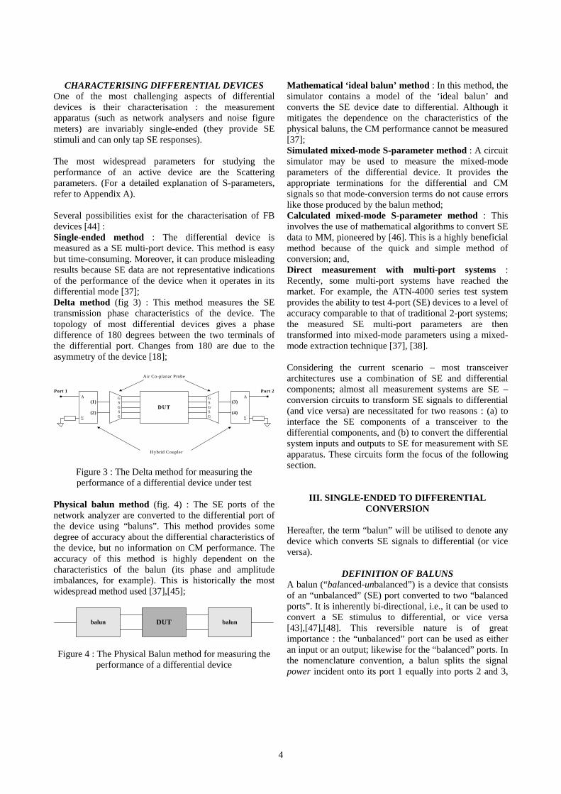
CHARACTERISING DIFFERENTIAL DEVICES One of the most challenging aspects of differential devices is their characterisation : the measurement apparatus (such as network analysers and noise figure meters) are invariably single-ended (they provide SE stimuli and can only tap SE responses). The most widespread parameters for studying the performance of an active device are the Scattering parameters. (For a detailed explanation of S-parameters, refer to Appendix A). Several possibilities exist for the characterisation of FB devices [44] : Single-ended method : The differential device is measured as a SE multi-port device. This method is easy but time-consuming. Moreover, it can produce misleading results because SE data are not representative indications of the performance of the device when it operates in its differential mode [37]; Delta method (fig 3) : This method measures the SE transmission phase characteristics of the device. The topology of most differential devices gives a phase difference of 180 degrees between the two terminals of the differential port. Changes from 180 are due to the asymmetry of the device [18];
DUT
Σ
Δ
Σ
Δ(1)
(2)
(3)
(4)
Port 1 Port 2GSGSG
GSGSG
Hybrid Coupler
Air Co-planar Probe
Figure 3 : The Delta method for measuring the performance of a differential device under test
Physical balun method (fig. 4) : The SE ports of the network analyzer are converted to the differential port of the device using “baluns”. This method provides some degree of accuracy about the differential characteristics of the device, but no information on CM performance. The accuracy of this method is highly dependent on the characteristics of the balun (its phase and amplitude imbalances, for example). This is historically the most widespread method used [37],[45];
DUTbalun balun
Figure 4 : The Physical Balun method for measuring the performance of a differential device
Mathematical ‘ideal balun’ method : In this method, the simulator contains a model of the ‘ideal balun’ and converts the SE device date to differential. Although it mitigates the dependence on the characteristics of the physical baluns, the CM performance cannot be measured [37]; Simulated mixed-mode S-parameter method : A circuit simulator may be used to measure the mixed-mode parameters of the differential device. It provides the appropriate terminations for the differential and CM signals so that mode-conversion terms do not cause errors like those produced by the balun method; Calculated mixed-mode S-parameter method : This involves the use of mathematical algorithms to convert SE data to MM, pioneered by [46]. This is a highly beneficial method because of the quick and simple method of conversion; and, Direct measurement with multi-port systems : Recently, some multi-port systems have reached the market. For example, the ATN-4000 series test system provides the ability to test 4-port (SE) devices to a level of accuracy comparable to that of traditional 2-port systems; the measured SE multi-port parameters are then transformed into mixed-mode parameters using a mixed-mode extraction technique [37], [38]. Considering the current scenario – most transceiver architectures use a combination of SE and differential components; almost all measurement systems are SE – conversion circuits to transform SE signals to differential (and vice versa) are necessitated for two reasons : (a) to interface the SE components of a transceiver to the differential components, and (b) to convert the differential system inputs and outputs to SE for measurement with SE apparatus. These circuits form the focus of the following section.
III. SINGLE-ENDED TO DIFFERENTIAL CONVERSION
Hereafter, the term “balun” will be utilised to denote any device which converts SE signals to differential (or vice versa).
DEFINITION OF BALUNS A balun (“balanced-unbalanced”) is a device that consists of an “unbalanced” (SE) port converted to two “balanced ports”. It is inherently bi-directional, i.e., it can be used to convert a SE stimulus to differential, or vice versa [43],[47],[48]. This reversible nature is of great importance : the “unbalanced” port can be used as either an input or an output; likewise for the “balanced” ports. In the nomenclature convention, a balun splits the signal power incident onto its port 1 equally into ports 2 and 3,

5
but as anti-phase voltages. When ports 2 and 3 are driven equally but in anti-phase, the balun combines the incident powers into the load terminating port 1 (fig. 5).
WHERE BALUNS ARE USED Inside a transceiver system using a combination of SE and differential components, baluns are necessary for interfacing the various components. These are often included on-chip. Some examples are : a multi-standard receiver with narrow-band baluns (one for each band) between SE filters and differential LNAs [27]; baluns for converting differential down-conversion mixer signal for SE processing [31]; baluns to transform the differential clock signal to SE [49]. Baluns are also deployed to measure differential signals using SE measurement systems. As an example, fig. 5 presents the use of baluns for characterising a differential amplifier. It is here important to compensate for the balun losses and the irregularities they introduce in the measurements [12],[50].
AC
Power SplitBalun
Power CombineBalun
DifferentialAmplifier
1
3
2
1
2
3
Single-EndedStimulus
Single-EndedResponse
A
Figure 5 : Measuring a differential amplifier using baluns Baluns may also form the end components of sub-systems (such as front-ends) so that they can be interfaced with other (SE) sub-systems to construct a complete transceiver. In such cases, the baluns are often placed off-chip or inter-chip. Some examples can be found in [9],[11],[12],[34],[38],[50],[51]. Sometimes, baluns fulfil the additional function of impedance matching, thus suppressing the impedance transformation loss [21],[48]. The most commonly used impedances of the “unbalanced” ports are 50Ω or 75Ω, and simple transformation ratios of 1:1, 1:2, and 1:4 are widely used. (This creates components with impedances in the ranges of 50:50, 50:100 and 50:200 for a 50Ω system). In particular instances, SE to differential converters improve the LO-to-RF isolation and isolate LNA resonators from the mixer [28].
PARAMETERS AND THEORY
Let us consider the balun as a power splitter (fig. 5, port 1 is excited with a SE stimulus; ports 2 and 3 give responses that are ideally equal in magnitude and 180° out of phase). The differential output voltage is VDM = V2 – V3, and the
differential current is IDM = (i2+i3)/2. The CM voltage and current are, respectively : VCM = (V2+V3)/2 and ICM = i2–i3. Ideally, V2 = -V3 and i2 = i3, cancelling out the CM terms. In an ideal balun, the signal voltage passes unchanged to the output ports (V2 = -V3 = V1), while the signal power undergoes a 3dB loss from port 1 to ports 2 and an identical loss to port 3 [40]. However, it is impossible to realise the ideal balun function. The voltage amplitude is attenuated (by a factor α) and its phase undergoes a shift (denoted by φ) in travelling through the balun. Moreover, ideally, the signals at the two terminals of the differential port are perfectly equal in magnitude and 180° out of phase for all frequencies. But in practice, the magnitudes of V2 and V3 are slightly different (let Δ denote this amplitude imbalance); similarly, there exists a phase imbalance between the two output signals away from the ideal 180° difference (denoted by the phase imbalance θ). Starting from the above definitions, we now proceed to an enumeration of the critical parameters that characterize a balun : Amplitude imbalance (Δ): The difference in attenuation between the two output signals, generally expressed as a maximum variation. In terms of the S-parameters :
Amplitude Imbalance = 20 log10|S31/S21| (2) Phase imbalance (θ) : The deviation from a 180 phase difference between ports, generally expressed as a maximum variation relative to 180° [43]. In terms of the S-parameters :
Phase Imbalance = ∠S21 - ∠S31 – 180° (3) The phase and amplitude imbalances are the two cardinal parameters in characterising any SE to balanced conversion circuit. Typically, split/combine imbalance is specified across a bandwidth. (For example, a typical specification of a 180° hybrid splitter is ±0.8dB amplitude imbalance and ±10° phase imbalance [52]). The effect of these imbalances is translated directly to the isolation between the two output ports [30]. The pre-eminence of either the phase imbalance or the amplitude imbalance is scenario- and application-dependant; and either the one or the other is more critical for signal cancellation [47]. Insertion loss : The attenuation in the signal amplitude. It is thus defined as the ratio between the outgoing power and the total incident power [13], [52]. For single-ended to differential conversion, the power incident on the input port is equally divided at the two output ports; thus, theoretically, all such conversions have a 3-dB loss between the input port and either of the two output ports.

6
The values given in balun datasheets and research results are those over and above the 3-dB loss. Isolation : Ideally, the two differential ports are completely isolated from one another. S-parameters S23 and S32 are the measure of the isolation between the two ports that together make up the differential port. Return Loss : The loss due to reflection at any port. It is characterised by the S-parameters S11, S22 and S33 Total loss : The total loss of a balun can be separated into two components : path loss and phase-error loss. Broken down into these two components, and represented in terms of S-parameters, this loss is [48] :
]**2²²
)cos(***2²²[log20]²²[log20)(31213121
312131213121
SSSSSSSSSSdBlossBalun error
++Θ++
−+−=
CMRR : Another way to determine the quality of a power splitter/combiner is suggested in the common mode rejection ratio. This is the ratio of the differential-mode gain to the common-mode gain. For a signal splitter or combiner, the CMRR is defined in terms of amplitude and phase imbalance by [13],[52] :
22
2θ+ΔΔ+
≈CMRR (5)
Impedances : Normally, baluns are connected to 50Ω systems, and all three ports must show a 50Ω characteristic impedance. Other variations also exist : unbalanced port impedances of 50Ω and 75Ω; balanced (to ground) port impedances of 12.5Ω, 25Ω, 37.5Ω, 50Ω, 75Ω, 100Ω have been encountered. (The differential balanced port impedance, as mentioned above, is twice the balanced-to-ground impedance of one of the constituent ports). Noise : Suppose the measured power gain (loss) and noise factor from port 1 to port 2 of the passive (active) input balun are G1 and F1. When port 1 is terminated with 50Ω, the noise PSD available at port 2 is kT*F1*G1 W²/Hz where k is the Boltzmann’s constant and T is the temperature. By symmetry, an equal noise power is also available at port 3. The noises at ports 2 and 3 are mutually uncorrelated. Similarly, the noise due to an output balun (with power gain G2 and noise factor F2 is kT*(F2-2)*G2 [40]. Signal quality : The nature of the signal after it has passed through the balun is important. Good indicators of the quality of the signal : transient amplitude difference between ports 2 and 3; DC offset of these signals, and total harmonic distortion (THD, expressed in percentage).
It is important that the signal be well matched to one another. Performance tradeoffs have invariably to be made between these parameters. The principal tradeoff is between frequency range, insertion loss and amplitude balance. Baluns can generally be separated into narrow band and broadband designs. For single-frequency applications the 10% bandwidth design (where the bandwidth is 10% of the working frequency) can achieve very low insertion loss (less than 0.2dB), but the amplitude balance will degrade rapidly away from the centre frequency. Octave bandwidth designs have more loss, but the amplitude balance is maintained over the octave range. Broadband designs are very sparingly used. It must be noted that because of the reversible nature of baluns and the nature of the S-parameters, the same definitions apply to a SE to differential balun as a differential-to-SE balun.
MEASURING A BALUN’S PERFORMANCE As instruments only measure in SE mode, the balun’s parameters have to be measured between ports 1 and 2, or ports 1 and 3. The third unused port is terminated with its characteristic impedance [40],[43]. Fig. 6 illustrates this 2-port characterisation of a balun’s noise figure using a noise figure meter.
Power SplitBalun
1
3
2
Noise FigureMeter
Power Combine
Balun
1
2
3
Noise FigureMeter
a B
Figure 6 : SE measurement of (a) an input balun and (b)
an output balun Another way to measure the characteristics of a balun using a 2-port vector network analyser is the back-to-back model, in which two equivalent baluns are connected back to back, their combined performance is measured, and averaged to give the performance of the balun. This type of measurement is important since it gives a good idea of the ‘differential’ action. For a passive splitter connected to a passive combiner, the SE cascade gain is 6dB greater than the sum of the SE gains of the two devices [40],[48]. An even better way to measure balun performance is by purely resistive terminations at two ports and the source voltage at the third [48].

7
Since the input and output typically have different impedances from each other, network analyzer calibration becomes more difficult.
HOW BALUN LIMITATIONS LIMIT SYSTEM
PERFORMANCE When incorporated into the system, baluns are often destined to interface circuits working at a certain frequency range. The balun has to be designed to have its optimum matching for the operating frequency. Accurate characterization thus becomes critical, and often limiting, in achieving optimal system-level performance [48]. When used to interface circuits to measurement apparatus, the baluns’ limited BW makes characterizing differential circuits across a wide frequency range tedious. Sometimes, the impedance ratio incompatibility makes certain measures impossible : for example, due to absence of a balun with desired impedance ratios at the frequency of interest, the IIP2 cannot be measured [27],[38]. Balun losses have to be calibrated out or de-embedded to attain the final performance of the device under test. But at present, there are no traceable calibration standards for balanced systems, and a standard error-correction methodology for balanced circuits has not been developed [10],[38]. Moreover, as MMICs advance, the need for broadband monolithic baluns that can be fabricated with the same technology becomes evident, and often impossible [24].
TYPES OF BALUNS Several options for the implementation of baluns exist. This section presents some of the major realisations of baluns : the ever-popular transformers and transmission lines, the rarer LC network realisation, and the rarest, but most interesting, transistor-based (“active”) baluns.
Transformers
A simple transformer can be converted to a balun by connecting the negative primary port to ground, thus making it SE on the primary winding side and differential on the secondary winding (fig. 7). Because of the ease of this realisation, a majority of balun structures are implemented using transformers.
Port 1 Port 2
Port 3
P : S
Figure 7 : Transformer connected to serve as a balun
The winding ratios of the transformers can be changed to give the desired impedance transformation along with the balun function. Lower turns ratio baluns operate at higher frequencies, but their lower impedance transformation reduces the overall conversion gain [21],[51]. A significant advantage is that such baluns introduce virtually no distortion to the RF signal [43]. The monolithic transformer remains the most popular for baluns, but cross-coupled and square-symmetric transformers are gaining in importance [27],[43],[53]. One major hindrance in transformer baluns is their incapacity for integration and often large sizes [14],[35]. However, recent advances have enabled a mitigation of the size problem to some degree : [25], for example, reports a Si-based mm-wave transformer with coupled symmetric inductors which occupies 45µmx45µm (a hundred-fold reduction compared to [43]). In addition to their prevalence in research findings, most of the industrially-available baluns are also transformer-based.
Planar waveguides and transmission lines The second most prevalent method of implementing baluns is using planar waveguides or micro-strip transmission lines (or a combination of the two). Fig. 8 presents a typical transmission-line type balun. The 20-40GHz MMIC balun reported in [24], for example, uses both coplanar waveguide and transmission lines. It is fabricated in an InGaP/GaAs HBT process, and occupies 0.7x1.4mm². Planar baluns are mostly fabricated in GaAs heterojunction technologies (no silicon-based planar solutions have been encountered thus far) [47].
Port 1
Port 2
Port 3
Figure 8 : Transmission line balun Sometimes, uni-planar slot-line baluns are also used, which combine unbalanced IMSL and unbalanced slot lines (fig. 9). Although these offer an improvement in the area occupied by the balun, they are still cumbersome (700×500µm²) [49],[54].

8
The Marchand balun offers a good trade-off between bandwidth and integration aspects, but its layout is typically too large for it to be integrated on-chip. A typical Marchand balun has an insertion loss better than 0.2dB and reflection coefficient S11 worse than -5dB [14], [55].
Port 1
Port 2
Port 3
Slot Line
Waveguide
Figure 9 : Combined waveguide-slot line balun Micro-strip baluns using quarter-wave lines are another variation of this class of baluns. They are designed with electromagnetic simulations [13],[21]. Other baluns which fall under the same category, the Lange, rat-race, and branch line couplers, require physical dimensions of the order of the signal wavelength and thus consume an unacceptably high chip area when operating below approximately 15GHz [13],[43].
LC Baluns Another class of baluns utilises passive LCR networks, and is a good option mainly because it exhibits higher potential for integration. They benefit, moreover, from small form factors : the balun in [14], for example, occupies only 180x160µm². Additionally such baluns allow impedance transformation [20]. Fig. 10 shows two such differential to SE balun implementations. Such baluns, however, are intrinsically narrow-band (since the LC network can only be tuned to a narrow band). The level of accuracy demanded from the passive elements is also very high (sometimes unattainably so) in order to reduce amplitude and phase imbalance between the two output ports.
Active Circuits The rarest class of balun structures, to which the present work hopes to add, consists of the use of transistors to realise the balun function. An active SE to differential converter will theoretically have the highest potential for integration and also the highest scope for a ‘programmable’ balun, with controllable performance.
VIN+
VIN-
VOUT
a
A -A
-2A
B
Figure 10 : Two LC baluns (these are differential to SE
converters and are not reversible) The commonest approach for an “active solution” makes use of the classic differential pair or its variations. The differential pair implementation in CMOS uses a simple comparator and level shifter to develop the desired output signals. This approach consumes very little area and power but yields highly distorted signals with a large offset (of the order of 600mV) [56]. Sometimes (for example, in [28]) a single transistor can be used to convert SE signals to differential, by providing the SE signal at the base and tapping the phase-inverted differential outputs at the collector and emitter (illustrated in fig. 11). The advantage over the classic differential pair is that it fulfils the high linearity requirements with a low supply and low current which the differential pair cannot. On the flip side, any such implementation is narrow-band, and it necessitates bulky and very accurately matched inductors and resistors (for good balance, the load impedances seen from the emitter and the collector must match well). FGMOS transistors with multiple gates can also be used to implement a differential to SE converter [57]. Here, the output signal is a function of the difference between the two inputs. This technique is advantageous in that it allows an expansion of the input signal range. The signals

9
obtained using this approach are distorted, with a THD of 0.3% for a 1kHz signal, and 1.2% for a 50MHz signal.
VIN
VOUT+
VOUT-
Figure 11 : Use of a single transistor to realise the balun function
Other Types
Among the least prevalent techniques for SE to differential conversion is the distributed divider circuit. While its promise lies in its excellent bandwidth, it is too large (typically 1.0×1.5mm²) to permit incorporation into chip [49].
BALUN PERFORMANCE COMPARISONS This section presents a comparison of the performances of the various balun implementations described above. Table I compares some baluns that have appeared in published literature. While very wideband baluns (up-to 40GHz) exist, there is often a price to be paid for their high bandwidths, in terms of high insertion loss: the balun in [24] has an insertion loss of at least 1.5dB as compared to 0.2dB for the narrow-band balun in [21]. The values given in tables 1 and 2 are over and above the 3-dB insertion loss that the signal suffers from ideally. Also, the higher the bandwidths, the larger are the amplitude and phase imbalances. The lowest amplitude imbalance encountered for any balun is 1dB. The various balun types have their specific advantages and drawbacks. In terms of size, transformer- and transmission-line based baluns are of the same order, while LC and active baluns are much smaller (minimum 500µm side for the former two compared to 150µm for the latter two). For monolithic implementation, the balun dimension is limited by the chip area, especially for frequencies below 20GHz. In such cases, active baluns are the only solution.
On the other hand, transformer baluns do not introduce any distortion to the signal, while active baluns do, sometimes to unacceptable levels.
Reference [24] [43] [47] [54] [21] [13] Range (GHz)
20– 40
0- 6
3- 18
0- 40
1.8– 2.3
1.5-3.0
Impedances Unbalanced 50Ω -** - - 50Ω - Balanced* 60Ω - - - 25Ω -
Losses Return >15dB - - - - - Insertion >1.5dB - - 1dB >0.2dB >1dB
Balance Amplitude ±1dB - 1.5dB >3dB >1dB - Phase 7° 5° 13° >20° >10° -
Single-Ended S-Parameters Best S11 -28B - - - - -3dB Best S21 -7dB –6dB -4dB - - -3dB BestS31 - -6dB -4dB - - -3dB Worst S32 - - -5dB - - - Worst S22 - - - - - -4dB Worst S33 - - - - - -6dB
*All balanced line impedances are given with respect to ground. The differential balanced line impedance is two times this value. ** Here, and in all further tables, the “-“ signifies that data is not available.
Table I : Comparative analyses of performance of some existent single-ended to differential converters
The variation of the output port impedances is impossible in LC networks, and almost always a feature of transformer-based baluns. From the multitude of industrially-available baluns, some were chosen, to showcase the widest range of operating frequency. Table II presents the performance of baluns furnished by three leading firms in the domain : Anaren Microwave (models 2425B50-50J [58] and 3A512 [59]), Johanson Technology (models 0900BL18B100 [60] and 0918BD41B050 [61]) and M/A-Com (models MABACT0034 [62] and MABAES0054 [63]). Provider Anaren Johanson M/Acom Reference [58] [59] [60] [61] [62] [63] Frequency (GHz)
2.4– 2.5
1.4– 1.6
0.8- 1.0
1.85- 1.92
0- 3.0
0- 1.0
Impedances Unbalanced 50Ω 50Ω 50Ω 50Ω 50Ω 50Ω Balanced* 100Ω 12.5Ω 50Ω 25Ω 50Ω 12.5Ω
Losses Return 22dB >15dB >9.5dB >8.5dB - - Insertion 0.65dB <0.3 <1.0dB <1.2dB 3.5dB <2.0dB
Balance Amplitude <±0.5dB 0.4dB <2.0dB 0.4dB <1.0dB <0.5dBPhase <±5° ±5° ±10° ±5° <20° <12°
*All balanced line impedances are given with respect to ground. The differential balanced line impedance is two times this value
Table II : Comparative analyses of performance of some
industrial baluns

10
As mentioned above, most of these are transformer-based. All (barring one) are narrow-band. Baluns with balanced port impedances of 12.5Ω, 25Ω, 50Ω, and 100Ω are encountered. Again, the wider the bandwidth, the worse is the insertion loss performance. The average phase imbalance is 10°.
Recent trends indicate that all future wireless communications receivers will be multi-band in order to cover multiple standards from the same hand-set. Sıngle-chip solutions are by far the best option. In order to reduce the number of components (and consequently, the size, cost and power consumption), it is necessary thaty the current method of having many narrow-band components in paralel and commutating between them be abandoned in favour of component-sharing. Baluns are also subject to the same constraints : they will have to be stable over large bandwidths, and be entirely integrable on the chip (active baluns are superior in this regard). As is evident from the comparisons presented above, balun solutions that fulfill both criteria (bandwidth and integration) simultaneously are non-existent. The following section presents a new solution that does fulfill both criteria.
IV. A NOVEL METHOD FOR SINGLE-ENDED TO DIFFERENTIAL CONVERSION
This section presents a new contribution to the implementation of single-ended to differential converters. The novel topology utilises the current conveyor as the basic building component.
THE CURRENT CONVEYOR Second-generation current conveyors (CCII) are widely used to realise analog electronics functions such as amplifiers, filters, active inductances, impedance converters and oscillators [64]. Such implementation benefit from the inherent advantages of current-mode signal processing : higher bandwidths, easier performance control, better distortion profiles, etc. CCIIs are active devices comprising three ports. The governing equation for the inter-relationship between these ports is given in matrix form as :
Figure 12 : 3-port representation of a CCII and its governing equations in matrix form
Each of the ports, X, Y and Z, presents an intrinsic parasitic impedance. The values of these impedances can be changed by varying the polarization current of the circuit, giving rise to the concept of the controlled current conveyor (CCC). It is this programmable characteristic that we will utilise. In its most elementary form, the CCII consists of a mixed trans-linear loop. Between the ports X and Y, it acts as a voltage follower; and between X and Z as current follower. Fig. 13 presents a basic CCII implementation using NPN-PNP transistors [65].
Figure 13 : “Classic” CCCII
In recent publications, many variations on this have been observed : CCCII with high RY [66]; NPN-PNP class-AB and all-NPN pseudo-class AB CCCIIs with low RX [67], [68]; CCCII with negative intrinsic resistance [69]; and fully differential conveyors [1], [6]. CCCIIs have been implemented in various technologies (bipolar technology with quasi-complementary n-p-n and p-n-p transistors remains the best). But pure CMOS conveyors also exist [70].
PRINCIPLE OF SINGLE-ENDED TO
DIFFERENTIAL CONVERSION Fig. 14 presents the principle of converting a single-ended signal to a differential one using current conveyor properties. The four blocks (designated 1 to 4) are current conveyors. The terminations of, and inter-connections between the different ports of the blocks are also given in the figure. The conversion of the positive polarity signal at the input VIN to a negative signal VOUT- is affected using blocks 1 and 2. In order to assure a maximum degree of symmetry (the determinant factor in phase and amplitude imbalance), blocks 1 and 2 are exactly identical, with the same polarisation current IO1 and IO2.

11
1
2
4
3
VOUT+
VOUT-
VINR1
R2
Y X
Y X
YX
Z
YZ
X
Figure 14 : Principle of the new single-ended to differential conversion scheme
Resistor R1 is used to fix the input port impedance to a constant value of 50Ω. Blocks 3 and 4 are current conveyors connected as voltage followers; they are exactly identical to each other; and their performance is controlled (using their respective biasing currents) to set the value for the output port impedances. TECHNOLOGY AND SIMULATION ENVIRONMENT For the design of the single-ended to differential converter, the technology parameters for transistors in 0.35µm SiGe BiCMOS from STMicroelectronics (BICMOS6G) were utilised. This is a high-end technology in which the NPN transistors have a transition frequency fT of around 45GHz. The circuit was simulated in the Cadence simulation environment for analog and mixed-mode circuits. The simulators Spectre and SpectreRF were used to carry out various analyses.
DESIGN METHODOLOGY A step-by-step design methodology was followed. Fırst of all, various current conveyor options were studied through simulation of their schematics and analysis of their performance. Final CCII topologies were settled upon, and their independant characteristics determined : performance in current-follower mode and in votlage follower mode. Parametric analyses were carried out where necessary (in order to determine optimum biasing currents, supply voltages and transistor dimensions). Additionally, the CCII architectures were modified in order to adapt them for the present purpose. The CCII characteristic that is of the highest importance is the -3dB bandwidth f-3dB in the current-follower mode. The phase of the output signal starts to trail off from the
ideal value - 0° or 180°- at a frequency of f-3dB/10; therefore, the highest possible bandwidth is necessary to ensure acceptable phase balance upto high frequencies. f-
3dB of up-to 12GHz was attained. Moreover, low distortion of the output signal is necessary : an upper limit of 1% was fixed for the THD of the signal. Various cominations of current conveyors were then connected according to the scheme presented in fig. 13 and their performance studied. Additional optimisation iterations were necessary for the conveyor blocks to determine the optimum performance of the SE to differential converter. Because the two signal paths (from VIN to VOUT+ and from VIN to VOUT-) contain a different number of active elements, additional care had to be taken that the two output signals be well matched to each other.
PERFORMANCE Circuit Conditions
The nominal supply voltage for the circuit is VDC = ±2.5V. Another version of the same circuit, which functions at ±2.2V, was also simulated. (Only the results for the ±2.5V version are presented here.) As mentioned earlier, the bias currents for block 1 (IO1) determines the input impedance of the circuit. It was set to a value that presented ZIN = 50Ω. To maintain symmetry, IO2 has the same value as IO1. The bias currents for voltage followers (blocks 3 and 4) determine the output impedance for the two output channels. Three different values were selected, which gave ZOUT of 50Ω, 75Ω and 100Ω. These values are the single-ended (that is, referenced to ground) impedances of each of the outputs, and the total differential fully-balanced impedance is two times this value. The optimum temperature at which the performance of this converter was determined is 27°C (300K). In later steps, this temperature was varied between to determine the temperature performance.
DC Response The single-ended to differential converter consumed 49mW, 42mW and 39mW from the stable ±2.5V supply, respectively, for output impedances of 50Ω, 75Ω and 100Ω.
AC Response Fıg. 15 presents a representative case of the amplitude and phase difference between the two outputs. As can be seen, there is an ideal balance for all frequencies from DC upto about 1GHz. In the low-frequency regime, the amplitude difference does not exceed 0.08dB and an ideal phase difference of 180° exists between the two output channels.

12
Fıgure 15 : Amplitude and phase balance, for ZOUT = 50Ω Table III presents the amplitude and phase imbalance between the differential output signals VOUT+ and VOUT-. The three different values are obtained for the three output port impedances.
ZOUT 50Ω 75Ω 100Ω Amplitude Imbalance
|VOUT+-VOUT-| 0.086dB 0.075dB 0.072dB Frequency at which magnitude difference is
1dB 1.82GHz 1.76GHz 1.74GHz 2dB 2.71GHz 2.65GHz 2.63GHz 3dB 3.23GHz 3.16GHz 3.13GHz
Phase Imbalance φ(VOUT+) - φ(VOUT-) 180° 180° 180° Frequency at which phase difference is :
5° 1.18GHz 1.24GHz 1.26GHz 10° 2.15GHz 2.20GHz 2.22GHz 15° 2.99GHz 2.98GHz 2.99GHz 20° 3.74GHz 3.67GHz 3.65GHz
Table III : Amplitude and phase balance, for different
values of ZOUT
For all the three values of the output impedance, the circuit evinces an excellent balance. Moreover, these performances are very similar to one another. For very strict balance requirements (1dB amplitude imbalance and 10° phase imbalance) the circuit can be utilised up-to 2GHz. However, as seen from tables I and II, these requirements are often eased (1dB and 20° balance); in these conditions, the circuit can operate up-to about 3GHz.
Noise Response The equivalent input noise was observed to be 3.34nV/√Hz, 3.38nV/√Hz, and 3.42nV/√Hz for ZOUT of 50Ω, 75Ω and 100Ω respectively.
Transient Response Figure 16 illustrates the nature of the two output signals.
Figure 16 : Transient signals VOUT+ and VOUT-; for ZOUT =
50Ω and VIN = 1mV ptp Table IV below presents the nature of the output signals for a 5mV peak-to-peak single-ended signals applied at the input. The results are given for three different values for the input signal frequency : 1kHz, 100kHz, and 100MHz.
ZOUT 50Ω 75Ω 100Ω Input signal : 5mV ptp; 1kHz
|VOUT+|, ptp 4.985mV 4.992mV 4.994mV THD (VOUT+) 0.009% 0.010% 0.010% |VOUT-|, ptp 4.944mV 4.956mV 4.960mV THD (VOUT-) 0.061% 0.061% 0.061%
Input signal : 5mV ptp; 100kHz |VOUT+|, ptp + 4.992mV 4.989mV 4.989mV THD (VOUT+) 0.010% 0.010% 0.010% |VOUT-|, ptp 4.938mV 4.951mV 4.951mV THD (VOUT-) 0.060% 0.064% 0.065%
Input signal : 5mV ptp; 100MHz |VOUT+|, ptp 4.991mV 4.997mV 4.994mV THD (VOUT+) 0.010% 0.009% 0.009% |VOUT-|, ptp 4.952mV 4.969mV 4.966mV THD (VOUT-) 0.483% 0.477% 0.486%
Table IV : Transient response, for different input signal
frequencies and different ZOUT It can be observed that the two output signals VOUT+ and VOUT- are excellently matched to the input signal as well as to each other : (a) VOUT+ and VOUT- attenuations are 0.2% and 1% of |VIN| respectively; and (b) on average, there is a 0.05mV (1% of |VIN|) difference between the amplitudes of VOUT+ and VOUT-. The distortion introduced to the signals can be summarized as : less than 0.06% THD for signal frequencies up-to 1MHz; and less than 0.5% THD for signal frequencies up-to 100MHz. Even signals of up-to 1GHz are distorted less than 1%. Moreover, for low-

13
frequency signals (1kHz), analyses showed that the THD remains below 1% for signals with amplitudes up-to 50mV ptp. The differences between the THDs of VOUT+ and VOUT- can be explained by the different number of transistors in the signal paths for the two outputs. This excellent value becomes even more prominent when compared to another ‘active’ balun implementation : [57], where the output signal has a THD of 0.3% for a 1kHz signal, and 1.2% for a 50MHz signal. The signals in another active baluns, presented in [56], are very highly distorted (although their distortion has not been quantified. As a further measure of the signal quality, an input step signal of 1µs pulse width and 1mV ptp amplitude was applied at the input. Very small peaks were observed in the VOUT+ and VOUT- responses. Pulse settling times (the time where the signal oscillations settle to within ±1% of the signal amplitude) of 0.07ns and 1.66ns were observed for the two output signals.
S-parameter Analysis The single-ended to differential converter was studied first as a three-port single-ended device; and then as a two-port device with one single-ended port (the input) and one balanced port (the output) (cf. Appendix A). All the results presented below are for ZIN = ZOUT+ = ZOUT- = 50Ω.
3-port Single-Ended Network In these analyses, the S-parameter responses were observed for the three combinations of two-ports. The unused port was terminated with 50Ω. Figure 17 below presents the nine single-ended S-parameters obtained from these analyses, for a frequency range of 1GHz to 5GHz. For frequencies up-to 3GHz, the return losses due to reflection of the three ports, denoted by S11, S22 and S33, respectively, remain lower than 10dB. Moreover, there is a good agreement between S22 and S33 (lower than 2dB difference), which testifies that the two output ports are symmetric. The single-ended insertion losses, represented by S21 and S31 are -3dB at low frequencies (up-to 1GHz). At higher frequencies of 3GHz, there is a loss of 0dB in the negative channel and 2dB in the positive channel. Thus, there is an improvement in the insertion loss at higher frequencies. The reverse signal gains S12 and S13, which quantify how much signal flows in the direction opposite to desired, are lower than –20dB for both channels for frequencies up-to 3GHz.
Finally, the isolation between the two output ports, represented by S23 and S32, remains better than 25dB up-to 3GHz. The differences between S23 and S32 can be attributed to the different signal paths in the two channels.
2-port Mixed-Mode Network Additionally, mixed-mode S-parameters were measured. These are important indicators of device symmetry and mode conversion. Here, port 1 signifies the input port and has only one signal component, single-ended; while port 2 consists of two components : differential mode and common mode. Fig. 18 presents the various mixed-mode S-parameters, for a frequency range of 1GHz to 5GHz. The input reflection coefficient SSS11 remains lower than -8dB up-to 3GHz. Moreover, the same values were obtained whether the output was connected in differential mode or in common mode, thus showing that the input reflection is totally independent of the output mode. When the output is in common-mode, its reflection (SCC22) is better than –10dB; whereas in differential mode it has a reflection (SDD22) better than -5dB up-to 3GHz. The differential insertion loss of the device (-SDS21), which is the best indicator of the insertion loss, is 0.6dB for frequencies up-to 2GHz and -0.8dB up-to 3GHz. When the device is differentially connected at the output, the reverse direction signal is very small (SSD12 is better than –24dB up-to 3GHz) The output signal is almost entirely differential mode, with the whole common-mode component being rejected (SCS21 : constant at –42dB at low frequencies, better than -15dB up-to 3GHz).
Temperature Performance The operating temperature of the circuit was varied from the nominal value of 27°C, to a range of –50°C to +50°C. This range was chosen because most of the industrially-available circuits are specified within it. The amplitude imbalance is lower than 0.22dB for all operating temperatures in the chosen range. Fig. 18 presents, as a function of the temperature, the frequency at which the amplitude imbalance exceeds 1dB and 3dB. For all temperatures, the 1dB imbalance is reached after 1.5GHz, 3dB imbalance is reached after 2.5GHz.

14
0
1
2
3
4
5
6
-60 -40 -20 0 20 40 60
Operating Temperature (°C)
Freq
uenc
y (G
Hz)
1dB amplitude imbalance3dB amplitude imbalance
Figure 19 : Amplitude Imbalance variation with operating
temperature Fig. 20 presents the phase imbalance performance within the same temperature range. Here, the y-axis presents the frequencies at which phase imbalance exceeds 10° and 20°. It can be seen that for all temperatures, phase imbalance is better than 10° up-to 1.5GHz and 20° up-to 2.5GHz.
0
1
2
3
4
5
6
-60 -40 -20 0 20 40 60
Operating Temperature (°C)
Freq
uenc
y (G
Hz)
10° phase imbalance 20° phase imbalance
Figure 20 : Phase Imbalance variation with operating
temperature
COMPARISONS AND DISCUSSIONS This section has described a new way of converting single-ended analog signals to differential. The new design, which makes use of the second generation current controlled conveyor, has shown a very promising performance when simulated. The design of the layout is currently underway and will soon be sent for fabrication in the 0.35µm SiGe BiCMOS technology of STMicroelectronics. To the best of the authors’ knowledge, this is the first wideband active balun which incorporates a variable output port impedance. Further, this variation is very easily realisable, by varying the circuit biasing current.
The promise of this new active balun is evident on comparison with the performances of structures, both passive and active, presented in other literature. In comparison with other active single-ended to differential converters, the new design gives rise to output signals that are minimally distorted. On a broader scale, on comparison with other major implementation schemes (active or passive), this balun shows an excellent bandwidth-balance characteristic thus easing the trade-of that has to be habitually made between these two parameters. The amplitude balance between the two output ports is by far the best encountered (0.08dB compared with 1dB). The balun gives a better overall S-parameter performance when compared to other baluns. Comparisons with industrial components further highlight this promise. While most other industrial baluns are narrow-band (typically specified over a 200MHz range), the new topology shows competitive performance from zero to 3GHz. The amplitude balance and phase balance are better, as is the return loss (by a factor of 5 to 10dB). One disadvantage of this topology (which it shares with LC- and active baluns, is that it is non-reversible, that is, it cannot be used to convert differential signals to single-ended. A topology which fulfils this function, and which is also based on the current conveyor is being developed.
V. CONCLUDING REMARKS This paper has endeavoured to add to the present understanding of differential circuits and their importance in wireless transceivers, especially for analog signal processing. Differential architectures and their relevant issues have been detailed. As things stand today, circuits that convert single-ended signals to differential (and vice versa) are an integral component : firstly, to interface the system’s single-ended constituents to its differential constituents; and secondly, to facilitate the measurement of differential device and system performance by making their inputs and outputs compatible with the single-ended ports of the measurement apparatus. Based on this significance, and due to the absence of any comprehensive review of such circuits in published literature, this paper has tried to cover all aspects of this conversion. Advancing one step further, the present work also proposes a novel scheme for the active implementation of the balun function, using current conveyors, a solution that exhibits excellent potential (testified on comparisons to other balun implementations, active and passive).

15
Figure 17 : Single-Ended 3-port S-Parameter Performance
Figure 18 : Mixed-mode 2-port S-Parameter Performance

16
REFERENCES 1. Alzaher, et al., A CMOS Fully Balanced Second-Generation Current Conveyor, IEEE TCAS-II, Vol. 50, No. 6, pp. 278 – 287, Jun. 2003 2. P. D. Applebee, Learn the Ins and Outs of Probing Those Tricky Differential Signals, Electronic Design Magazine, pp. 72 – 79, Apr. 1999 3. P. J. Hurst, et al., Determination of Stability Using Return Ratios in Balanced Fully Differential Feedback Circuits, IEEE TCAS-II, Vol. 42, No. 12, pp. 805 - 817, Dec. 1995 4. J. Mulder, et al., A Reduced-Area Low-Power Low-Voltage Single-Ended Differential Pair, IEEE JSSC, Vol. 32, No. 2, pp.254 – 257, Feb. 1997 5. H. Alzaher, et al., A CMOS Fully Balanced Differential Difference Amplifier and Its Applications, IEEE TCAS Transactions Briefs, Vol. 48, No. 6, pp. 614 - 620, June 2001 6. A. A. El-Adawy, et al., A Novel Fully Differential Current Conveyor and Applications for Analog VLSI, IEEE TCAS-II, Vol. 47, No. 4, pp. 306 - 313, Apr. 2000 7. V. I. Prodanov, et al., A Differential Active Load and its Applications in CMOS Analog Circuit Designs, IEEE TCAS-II, Vol. 44, No. 4, pp. 265 - 273, Apr. 1997 8. F. Gatta, et al., A 2-dB Noise Figure 900-MHz Differential CMOS LNA, IEEE JSSC, Vol. 36, No. 10, pp.1444 – 1452, Oct. 2001 9. J. J. Zhou, et al., Monolithic Transformers and Their Application in a Differential CMOS RF Low-Noise Amplifier, IEEE JSSC, Vol. 33, No. 12, pp.2020 – 2027, Dec. 1998 10. H. Sjöland, et al., A Merged CMOS LNA and Mixer for a WCDMA Receiver, IEEE JSSC, Vol. 38, No. 6, pp.1045 – 1050, Jun. 2003 11. D. J. Cassan, et al., A 1-V Transformer-Feedback Low-Noise Amplifier for 5-GHz Wireless LAN in 0.18µm CMOS, IEEE JSSC, Vol. 38, No. 3, pp.427 – 435, Mar. 2003 12. K. L. R. Mertens, et al., A 700-MHz 1-W Fully Differential CMOS Class-E Power Amplifier, IEEE JSSC, Vol. 37, No. 2, pp.137 – 141, Feb. 2002 13. K-C Tsai, et al., A 1.9-GHz, 1-W CMOS Class-E Power Amplifier for Wireless Communications, IEEE JSSC, Vol. 34, No. 7, pp.962 – 970, Jul.1999 14. W. Bakalski, et al., A Fully Integrated 5.3-GHz 2.4-V 0.3-W SiGe Bipolar Power Amplifier With 50Ω, IEEE JSSC, Vol. 39, No. 7, pp.1006 – 1014, Jul. 2004 15. P. J. G. van Lieshout, et al., A Power-Efficient, Low-Distortion Variable Gain Amplifier Consisting of Coupled Differential Pairs, IEEE JSSC, Brief Papers, Vol. 32, No. 12, pp.2105 – 2100, Dec. 1997 16. J. J. F. Rijns, CMOS Low-Distortion High-Frequency Variable-Gain Amplifier, IEEE JSSC, Brief Papers, Vol. 31, No. 7, pp.1029 – 1034, Jul. 1996
17. F. Centurelli, et al., A Bootstrap Technique for Wideband Amplifiers, IEEE TCAS–1, Vol. 49, No. 10, pp. 1474 – 1480, Oct. 2002 18. H-T Ahn, et al., A 0.5–8.5-GHz Fully Differential CMOS Distributed Amplifier, IEEE JSSC, Vol. 37, No. 8, pp. 985 – 993, Aug. 2002 19. Z. Y. Chang, et al., A CMOS Differential Buffer Amplifier with Accurate Gain and Clipping Control, IEEE JSSC, Vol. 30, No. 7, pp. 731 – 735, Jul. 1995 20. J. Durec, An Integrated Silicon Bipolar Receiver Subsystem for 900-MHz ISM Band Applications, IEEE JSSC, Vol. 33, No. 9, pp. 1352 – 1372, Sep. 1998 21. I. Takenaka, et al., L/S-Band 140-W Push–Pull Power AlGaAs/GaAs HFET’s for Digital Cellular Base Stations, IEEE JSSC, Vol. 34, No. 9, pp. 1181 – 1187, Sep. 1999 22. C. Q. Wu, et al., 40-GHz Transimpedance Amplifier With Differential Outputs Using InP–InGaAs Heterojunction Bipolar Transistors, IEEE JSSC, Vol. 38, No. 9, pp. 1518 - 1523, Sep. 2003 23. Y. Degerli, et al., Non-Stationary Noise Responses of Some Fully Differential On-Chip Readout Circuits Suitable for CMOS Image Sensors, IEEE TCAS–II, Vol. 46, No. 12, pp. 1461 – 1474, Dec. 1999 24. K. W. Hamed, et al., A Monolithic Double-Balanced Direct Conversion Mixer With an Integrated Wideband Passive Balun, IEEE JSSC, Vol. 40, No. 3, pp. 622 – 629, Mar. 2005 25. T. O. Dickson, et al., A 2.5-V, 40-Gb/s Decision Circuit Using SiGe BiCMOS Logic, Proc. of 2004 Symp/ on VLSI Circuits, pp. 206 – 209, 2004 26. C-H Lee, et al., Current-Mode Approach for Wide-Gain Bandwidth Product Architecture, IEEE TCAS–II, Transactions Briefs, Vol. 45, No. 5, pp. 626 – 632, May 1998 27. Adiseno, et al., A Wide-Band RF Front-End for Multiband Multistandard High-Linearity Low-IF Wireless Receivers, IEEE JSSC, Vol. 37, No. 9, pp. 1162 – 1168, Sep. 2002 28. J. Ryynänen, et al., A Dual-Band RF Front-End for WCDMA and GSM Applications, 1198-1204 IEEE JSSC, Vol. 36, No. 8, pp. 1198 – 1204, Aug. 2001 29. P. Rossi, et al., A Variable Gain RF Front-End, Based on a Voltage–Voltage Feedback LNA, for Multistandard Applications, IEEE JSSC, Vol. 40, No. 3, pp. 690 – 697, Mar. 2005 30. Ma. L. de la Fuente, et al., Low-Noise Ku-Band MMIC Balanced P-HEMT Upconverter, IEEE JSSC, Vol. 34, No. 2, pp. 259 – 263, Feb. 1999 31. D. S. Malhi, et al., SiGe W-CDMA Transmitter for Mobile Terminal Application, IEEE JSSC, Vol. 38, No. 9, pp. 1570 – 1574, Sep. 2003 32. Y. Le Guillou, et al., Highly Integrated Direct Conversion Receiver for GSM/GPRS/EDGE With On-Chip 84-dB Dynamic Range Continuous-Time ΣΔ ADC, IEEE JSSC, Vol. 40, No. 2, pp. 403 – 411, Feb. 2005

17
33. J. P. Maligeorgos, et al., A Low-Voltage 5.1–5.8-GHz Image-Reject Receiver with Wide Dynamic Range, IEEE JSSC, Vol. 35, No. 12, pp. 1917 – 1926, Dec. 2000 34. A. Rofougaran, et al., A Single-Chip 900-MHz Spread-Spectrum Wireless Transceiver in 1µm CMOS — Part I: Architecture and Transmitter Design, IEEE JSSC, Vol. 33, No. 4, pp. 515 – 534, Apr. 1998 35. S. Y. Yue, et al., A 17.1–17.3-GHz Image-Reject Downconverter With Phase-Tuneable LO Using 3 Subharmonic Injection Locking, IEEE JSSC, Vol. 39, No. 12, pp. 2321 – 2332, Dec. 2004 36. J. Jussila, et al., A 22-mA 3.0-dB NF Direct Conversion Receiver for 3G WCDMA, IEEE JSSC Brief Papers, Vol. 36, No. 12, pp. 2025 – 2029, Dec 2001 2025 37. G. Amorese, et al., RF Balanced Device Characterization, Presentation for Agilent Technologies, 14/01/2003 38. B. Cole, Fully Characterize Balanced Devices, Microwave and RF Magazine, pp. 90 – 99, Jan. 1999 39. S. M. Park, et al., 1-Gb/s 80-dB Fully Differential CMOS Transimpedance Amplifier in Multichip on Oxide Technology for Optical Interconnects, IEEE JSSC, Vol. 39, No. 6, pp. 971- 974, Jun. 2004 40. A. A. Abidi, et al., De-Embedding the Noise Figure of Differential Amplifiers, IEEE JSSC, Vol. 34, No. 6, pp. 882 – 885, Jun. 1999 41. W. Sansen, Distortion in Elementary Transistor Circuits, IEEE TCAS—II, Vol. 46, No. 3, pp. 315 – 325, Mar. 1999 42. G. Xu, et al., A Systematic Approach in Constructing Fully Differential Amplifiers, TCAS-II, Vol. 47, No. 12, pp. 1547 – 1550, Dec. 2000 43. J. R. Long, Monolithic Transformers for Silicon RF IC Design, IEEE JSSC, Vol. 35, No. 9, pp. 1368 – 1382, Sep. 2000 44. L. Betts, Theory and Analysis of Differential Measurement Techniques, Applied Microwave and Wireless Magazine, pp. 70 – 76, 2001 45. G. Sundberg, Understanding Single-Ended and Mixed-Mode S-parameters, in 4 parts, Microwave and RF Magazine, Mar., Apr., May, Jun. 2001 46. D. E. Bockelman and W. R. Eisenstadt, Combined Differential and Common-Mode Scattering Parameters : Theory and Simulation, IEEE Trans. on MTT, Vol. 43, No. 7, pp. 1530 – 1539, Jul. 1995 47. D. E. Meharry, et al., Broad Bandwidth Transformer Coupled Differential Amplifiers for High Dynamic Range, IEEE JSSC, Vol. 34, No. 9, pp. 1233 – 1238, Sep. 1999 48. B. E. Wilcox, Determine the Loss of Discrete Baluns, Microwaves and RF Magazine, pp. 103 - ?, Jan. 1998 49. K. Murata, et al., A Distributed Selector IC Using GaAs MESFET’s with Multilayer-Interconnection Structure, IEEE JSSC, Vol. 35, No. 2, pp. 258 – 267, Feb. 2000
50. T-P Liu, et al., 5-GHz CMOS Radio Transceiver Front-End Chipset, IEEE JSSC, Vol. 35, No. 12, pp. 1927 – 1933, Dec. 2000 51. J. P. Maligeorgos, et al., A Low-Voltage 5.1–5.8-GHz Image-Reject Receiver with Wide Dynamic Range, IEEE JSSC, Vol. 35, No. 12, pp. 1917 – 1926, Dec. 2000 52. D. E. Bockelman and W. R. Eisenstadt, Combined Differential and Common-Mode Analysis of Power Splitters and Combiners, IEEE Trans. on MTT, Vol. 43, No. 11, pp. 2627 – 2632, Nov. 1995 53. D. J. Cassan, et al., A 1-V Transformer-Feedback Low-Noise Amplifier for 5-GHz Wireless LAN in 0.18µm CMOS, IEEE JSSC, Vol. 38, No. 3, pp.427 – 435, Mar. 2003 54. M. Nakamura, et al., Over-30-GHz Limiting Amplifier IC’s with Small Phase Deviation for Optical Communications Systems, IEEE JSSC, Vol. 31, No. 8, pp. 1091 – 1099, Aug. 1996 55. A.B. Smolders, et al., Wide-band Antenna Element with Integrated Balun, - 56. Y. Toh, et al., Single-Ended to Differential Converter for Multiple-Stage Single-Ended Ring Oscillators, IEEE JSSC, Vol. 38, No. 1, pp. 141 – 145; Jan 2003 57. S. Vlassis, et al., Differential-Voltage Attenuator Based on Floating-Gate MOS Transistors and Its Applications, IEEE TCAS-I, Vol. 48, No. 11, pp. 1372 – 1378, Nov. 2001 58. Model 2425B50-50J Ultra low Profile 0805 Balun 50Ω to 100Ω Balanced product datasheet, Anaren Microwave 59. Model 3A512 Balun 50Ω to 12.5Ω Balanced product datasheet, Anaren Microwave 60. 900 MHz Balun P/N 0900BL18B100 product datasheet, Johanson Technology 61. 920/1885 MHz Dual Band Balun P/N 0918BD41B050 product datasheet, Johanson Technology 62. MABACT0034 1:1 Tx Line Balun Transformer 4.5 – 3000 MHz product datasheet, M/A-Com 63. MABAES0054 E-series 4:1 Transmission Line Transformer 5.0 – 1000.0 MHz product datasheet, M/A-Com 64. F. Seguin, et al., A gain-controllable wide-band low-noise amplifier in low-cost 0.8-µm Si BiCMOS technology, IEEE Trans. on MTT, Vol. 52, No. 1, pp. 154 – 160, Jan. 2004 65. A Fabre, et al., High frequency applications based on a new current controlled conveyor, IEEE TCAS–I, Vol. 43, No. 2, pp. 82 – 91, Feb. 1996 66. M. Alami, et al., Second Generation Current Conveyors with enhanced input resistance, Intl. Journal of Electronics; Vol. 86, No. 4; pp. 405 – 412, 1999 67. F. Seguin, et al., New Second-Generation Current Conveyor with Reduced Parasitic Resistance and Bandpass Filter Application, IEEE TCAS-I, Vol. 48, No. 6, pp. 781 – 785, Jun. 2001

18
68. F. Seguin, et al., 2.2 GHz All-n-p-n Second-Generation Controlled Conveyor in Pseudo-class AB Using 0.8-µm BiCMOS Technology, IEEE TCAS-II, Vol. 51, No. 7, pp/ 369 – 373, Jul. 2004 69. H. Barthélemy, et al., A Second Generation Current-Controlled Conveyor With Negative Intrinsic Resistance, IEEE TCAS—I, Transactions Briefs, Vol. 49, No. 1, pp. 63 – 65, Jan. 2002 70. I. A. Awad, et al., New CMOS Realization of the CCII-, IEEE TCAS—II, Vol. 46, No. 4, pp. 460 – 463, Apr. 1999
APPENDIX A : REVIEW OF SCATTERING
PARAMETERS In the past, differential communication circuits operated at low frequencies, where they could be designed and analyzed using lumped-element models and techniques. With the frequency of operation increasing beyond 1GHz, this lumped-element approach is no longer valid, because the physical size of the circuit approaches the size of a wavelength. Distributed models and analysis techniques are now used instead of lumped-element techniques. Scattering parameters, or S-parameters, have been developed for this purpose. These Scattering (or S-) parameters are widely accepted for characterizing the linear response of high frequency networks. They represent a scattering or separation of a signal by a device under test. These scattered signals are the reflected and transmitted waves that are produced when a device is struck with an incident wave.
2-PORT S-PARAMETERS A ratio of the incident and the outgoing wave is used.
jkforaabS k
j
iij ≠== 0 (A.1)
To measure Sij, port j is energized and the response is measured on port i. All ports, except the stimulus port, must be terminated with that port's characteristic impedance (typically 50Ω).
[ ] [ ][ ]aSb = (A.2)
[b] is an nx1 column matrix, [a] is an nx1 column matrix, and [S] is an nxn matrix, where n is the number of ports in the network. In the [S] matrix, the diagonal elements S11 and S22 are the reflection coefficients if and only if all other ports are terminated with their characteristic impedance. The voltage standing wave ratio (VSWR), the return loss and other parameters can be calculated from this. S12 and S21 are the transmission coefficients. From this quantity, gain in an active device, loss in a passive device, insertion loss, group delay, and other related parameters can be found.
MULTI-PORT DEVICES A multi-port device is any network with more than a single input and a single output. Each port is comprised of two terminals. When one terminal connection is used to transmit the RF signal and the other is used as a ground reference, the port is referred to as single-ended. Traditionally, most RF devices have been designed to operate in this mode. When a terminal is designed to reference a signal on another terminal, it is operating in a differential mode. The terminal pair is known as a differential or balanced port. Any signal that is common or in-phase to both terminals will ideally be rejected, and will not pass through the circuit.
4-PORT DEVICES The S-parameter matrix of a multi-port network must be expanded to n² elements, where n is the number of network ports. Fig. A.1 illustrates a 4-port device, in its single-ended connection, and differential port connection. The numbering scheme for the ports is universally-accepted and must be strictly adhered to.
Port 1
Port 3
Port 2
Port 4
Port 1 Port 2
+ +
--
A 4-port Single-ended Device
A 2-port Differential Device
Figure A.1 : Representing a differential device : as 4-port SE and as 2-port balanced
4-port : Single-ended S-parameters
This approach treats the component as a single-ended device. To measure the S-parameters for this single-ended approach using a two-port vector network analyzer (VNA), terminate the two unused ports with 50Ω and measure the two-port S-parameters for the two un-terminated ports. This method is very popular for the characterisation of differential devices. The matrix-form notation is given in fig. A.2.
⎥⎥⎥
⎦
⎤
⎢⎢⎢
⎣
⎡
44434241
34333231
24232221
14131211
SSSSSSSSSSSSSSSS
StimulusPorts
ResponsePorts
Figure A.2 : 4-port single-ended S-parameters
4-port Mixed-mode S-parameters For differential devices, single-ended S-parameters do not provide much insight into the circuit’s differential (or common-mode) operation. They can be misleading, or at best difficult to interpret. The S-parameter definition needs to be expanded to independently consider each mode in which a balanced device will operate. As in single-ended S-parameters, the voltages and currents defined on the balanced ports can be used to define a set of normalized power waves. The difference is that these new
19
mixed-mode normalized power waves are now mode specific. By again taking a ratio of the normalized response and incident power waves, a set of mixed-mode S-parameters can be defined. Conceptually the new 4x4 matrix can be sub-divided into four quadrants that symbolize four separate modes of operation: DD, CC, CD, and DC. Each quadrant gives the input and output reflection characteristics and the forward and reverses transmission characteristics for that mode.
Sghij = S(output-mode)(input-mode)(output-port)(input-port)
⎥⎥⎥
⎦
⎤
⎢⎢⎢
⎣
⎡
22212221
12111211
22212221
12111211
CCCCCDCD
CCCCCDCD
DCDCDDDD
DCDCDDDD
SSSSSSSSSSSSSSSS
Common-modeStimulus
Port 1 Port 2 Port 1 Port 2
Differential-modeStimulus
Port 1
Port 2
Port 1
Port 2
Differential-mode
Response
Common-mode
Response
Figure A.3 : Mixed-mode S-parameter matrix for a differential device
Differential-mode (DD) quadrant, in the upper-left corner of the mixed-mode S-parameter matrix, describes the behaviour of the circuit with a differential stimulus and differential response. These parameters describe the input and output reflections, and the forward and reverse transmissions in the differential mode. Common-mode (CC) quadrant, in the lower-right corner describes the behaviour of the circuit with a common-mode stimulus and common-mode response. By comparing the differential gain from the DD quadrant to the common-mode gain of the CC quadrant, the common- mode rejection ratio (CMRR) can be determined. These parameters describe the input and output reflections, and the forward and reverse transmissions in the common mode. Differential-to-common-mode-conversion (CD) quadrant, in the lower-left corner, describes the behaviour of the circuit with a differential stimulus and common-mode response. In an ideal balanced device, these terms are all equal to zero, that is, there is no mode conversion. In practice, there will be some amount of mode conversion. The more mode conversion from differential-mode to common-mode that exists, the more likely there will be EMI radiation from the system. As the device becomes asymmetrical, these terms become larger. Therefore, they provide a measure of the device symmetry. Common-mode-to-differential-conversion (DC) quadrant, in the upper-right corner, describes the behaviour of the circuit with a common-mode stimulus and differential- mode response. Again, in an ideal balanced device, these terms are all equal to zero. The more mode conversion from common-mode to differential-mode that exists, the more susceptible the system will be to common-mode noise, either as ground noise or EMI.
Conversion from Single-ended to mixed-mode S-parameters To convert from single-ended S-parameters to mixed-mode S-parameters, it is assumed that the device under test is being fed from differential input lines.
1−= MSMS stdmm (A.3) where
⎥⎥⎥
⎦
⎤
⎢⎢⎢
⎣
⎡−
−=
1100001111000011
21M
The above formula provides a straight-forward transformation between single-ended and mixed-mode S-parameters.
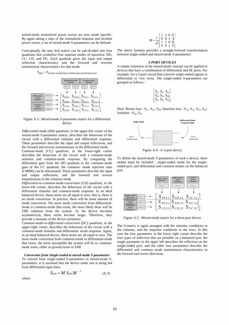
3-PORT DEVICES A simple extension of the mixed-mode concept can be applied to devices that have a combination of differential and SE ports. For example, for a 3-port circuit that converts single-ended signals to differential or vice versa. The single-ended S-parameters are goruped as follows :
⎥⎥
⎦
⎤
⎢⎢
⎣
⎡
333231
232221
131211
SSSSSSSSS
Here, Return loss : S11, S22, S33; Insertion loss : S13, S12, S21, S31; Isolation : S32, S23
Port 1(unbalanced)
Port 2(balanced)
Single-endedDifferential Mode
Common Mode
Figure A.4 : A 3-port device
To define the mixed-mode S-parameters of such a device, three modes must be included : single-ended mode for the single-ended port, and differential and common-modes on the balanced port.
C om m on-m od e
Stim ulus
P ort 1 Port 2 Port 2
Sin gle-end edStim ulus
Port 2
Port 2 ⎥⎥
⎦
⎤
⎢⎢
⎣
⎡
2 22 22 1
2 22 22 1
1 21 21 1
C CC DC S
D CD DD S
S CS DS S
SSSSSSSSS
D ifferential-m ode
Stim u lus
P ort 1Sin gle-end edR esp onse
D ifferentia l-m ode
R esp onseC om m on-
m odeR esp onse
Figure A.5 : Mixed-mode matrix for a three-port device
The S-matrix is again arranged with the stimulus conditions in the columns, and the response conditions in the rows. In this case the four parameters in the lower right corner describe the four types of reflection that are possible on a balanced port, the single parameter in the upper left describes the reflection on the single-ended port, and the other four parameters describe the differential and common mode transmission characteristics in the forward and revere directions.


