StandAlone – next generation functional electrical stimulator · Second Year Group Project...
39
Imperial College London, Electrical and Electronic Engineering Second Year Group Project Project Report StandAlone – next generation functional electrical stimulator Website: www.ee.ic.ac.uk/navneeth.jayan11/yr2proj/default.htm By: Asquini, Amedeo Badmos, Olatomiwa Jayan, Navneeth Upmanyu, Aashish Date: 03 March 2013 Special Thanks to: Bucci, Giovanni (Prof.) Eftekhar, Amir (Dr.) Onori, Luciano (Prof.) Pike T., William (Dr.) Zobel B., Pierluigi (Prof.) Sponsored By: Acme Systems srl (for hardware of prototype)
Transcript of StandAlone – next generation functional electrical stimulator · Second Year Group Project...

Imperial College London, Electrical and Electronic Engineering
Second Year Group Project
Project Report
StandAlone – next generation functional electrical stimulator
Website: www.ee.ic.ac.uk/navneeth.jayan11/yr2proj/default.htm
By:
Asquini, Amedeo
Badmos, Olatomiwa
Jayan, Navneeth
Upmanyu, Aashish
Date: 03 March 2013
Special Thanks to:
Bucci, Giovanni (Prof.)
Eftekhar, Amir (Dr.)
Onori, Luciano (Prof.)
Pike T., William (Dr.)
Zobel B., Pierluigi (Prof.)
Sponsored By:
Acme Systems srl (for hardware of prototype)

Group Project, Proposal 7 Functional Electrical Stimulator
Page 2 of 39
TABLE OF CONTENTS
Preview……………………………………………………………………………………………………… 3
1. Introduction ....................................................................................................................... 3
2. Motivation ........................................................................................................................... 3 Technical Section…………………………………………………………………………………… 3 -10
1. System Design Criteria .................................................................................................... 4 1.1. Optimal Signal Generation criteria .................................................................................. 4 1.2. Additional Features ............................................................................................................... 4
2. Design and Implementation.......................................................................................... 5 2.1. Linux board and FPGA implementation ......................................................................... 6 2.2. Sensor Interfacing .................................................................................................................. 7 2.3. Voltage-to-current converter ............................................................................................. 7 2.4. Biphasic stimulation with single power supply ........................................................... 7 2.5. High Voltage Generation ...................................................................................................... 8 2.6. Safety Circuit ............................................................................................................................ 8
3. Scalability and Flexibility ............................................................................................... 8
4. Power Consumption ........................................................................................................ 9
5. Further Improvements ................................................................................................... 9 Economic Feasibility and Business Plan……………………………………………… 10-11
1. Cost ..................................................................................................................................... 10
2. Business Plan .................................................................................................................. 11 Conclusion…………………………………………………………………………………………… 11-12
REFERENCES ............................................................................................................................ 12
APPENDIX A ............................................................................................................................. 13
APPENDIX B ............................................................................................................................. 14
APPENDIX C .............................................................................................................................. 15
APPENDIX D ............................................................................................................................. 16
APPENDIX E.............................................................................................................................. 25
APPENDIX F .............................................................................................................................. 27
APPENDIX G ............................................................................................................................. 33
APPENDIX H ............................................................................................................................. 36
APPENDIX I............................................................................................................................... 38
APPENDIX J ............................................................................................................................... 39

Group Project, Proposal 7 Functional Electrical Stimulator
Page 3 of 39
Preview
1. Introduction This report discusses the design and implementation of a low cost and fully programmable device
that can be used for various Functional Electrical Stimulation (FES) applications.
FES is the use of electrical stimulation to generate or restore specific motor functions [1]. This is
done by passing a charge to nerves controlling muscles and neuronal structures in which
functionality has been limited or completely compromised due to illnesses or traumas such as
Spinal Cord Injury (SCI), Multiple Sclerosis (MS), Stroke (cerebrovascular accident), Traumatic
Brain Injury (TBI), Brain tumour, or Cerebral Palsy (CP)[2]. Such techniques have been proven
to be effective but still suffer from numerous bottlenecks that have prevented their widespread
use. This report aims at presenting a functional stimulator module that can address some of these
limitations, as detailed in the technical section.
It should be noted that for the purposes of this report we have implemented a proof-of-concept
prototype of the signal generator (an integral part of the stimulator) and designed the other stages
to be interfaced with it. Although one stimulation channel was used, the design has been made
such that it can be scaled to as many channels as required with minimal additional effort (c.f. §3,
Technical).
2. Motivation As of 2012, there are 40,000 people with Spinal Cord Injury (SCI) in the UK [3] and
approximately 270,000 people in the US [4] with 1095 per year being added in the UK [3] and
12,000 per year in the US [4]. Additionally, the cost related to care of patients with SCI is
astounding: approximately £ 46,500 per person per year in the US and an estimated £500 million
for the SCI affected population in the UK. (See Appendix A)
Moreover, commercially available solutions are designed for very specific purposes. Hence, their
employment on a widespread basis requires costly hardware and software changes making it
unfeasible from a technical and business point of view. This is believed to be the main reason
why these devices have been unsuccessful in penetrating the market; in fact FES technologies are
believed to have only addressed less than 10% of the potential market [5][6]. Additionally, many
of these devices are expensive and require expert care to be maintained and be effective in the
long run. Lastly, the main limitation of current FES techniques is that they induce much higher
neuromuscular fatigue than natural movement [7], making their everyday use undesirable.
Therefore, the aim of this study was to design a device that could overcome all these problems, be
low-cost, effective, fully programmable and user-friendly. By doing so, we wanted to be able to
provide practitioners with a universal hardware platform, using which they can create custom
neuroprostheses, conduct electro-physiological studies and develop neurological assessment
devices.
Technical Section In order for the best performance to be guaranteed, several criteria regarding signal generation
need to be met, so the choice of the parameters of the electrical signals activating the nerve fibres
and muscles has to be accurate. Many studies have been conducted to investigate muscle response
to different pulse frequencies, amplitudes and durations [7]. The emphasis of this section,
therefore, is not determining the optimal values of the aforementioned quantities, but creating a
novel design with the ability to generate stimulating signals with parameter value range similar to
those used in currently available systems. Chosen parameter values and those from existing
products are presented in Appendix B.
We present here the thinking-process behind our product and its merits from a technical point of
view.

Group Project, Proposal 7 Functional Electrical Stimulator
Page 4 of 39
1. System Design Criteria
The following sub-sections discuss in some detail the characteristics of our system, including the
nature of the constraints that had to be accounted for, and reasons behind the choice of certain
features. Additional features geared more towards user-friendliness and programmability for
practitioners and users were also accounted for in our design criteria. Another section outlines
further improvements that could be made to this product to render it even more useful.
1.1. Optimal Signal Generation criteria
It is important to gain some understanding regarding the essential characteristics the output
signals need to have. These characteristics are mainly determined by constraints imposed by user
safety amongst other issues. It is essential to acquire this understanding, as this would largely
influence the software and hardware design. The factors that need to be considered are:
1. Current signals are preferred to voltage signals since the former are independent of tissue and
electrode contact resistance [2] (within current limits). Responses that are independent of the
resistance can also provide more reliable and reusable results in FES studies. Hence a voltage
to current converter will have to be implemented;
2. Biphasic stimulation is preferred to monophasic stimulation since the latter causes an alteration
in the tissue ionic distribution (hence polarization), which inevitably results in substantial
tissue damage, pain and electrode degradation (and reduced lifetime) [8]. More specifically,
the desired charge balance can be ensured with balanced biphasic stimulation. This further
reduces unnatural ion build up since it ensures that the charge displaced during the positive
phase of the pulse is equal to that in the following negative phase. Our stimulator will
therefore have to guarantee the possibility to generate current signals in both directions
(positive and negative) for every single channel;
3. A long signal rise time could result in accommodation of the membrane potential to the
stimulus and in the worst case prohibit the potential membrane threshold to be attained, thus
not resulting in the expected neuromuscular response [9]. This phenomenon is known as nerve
accommodation and must be avoided to allow excitation of a response with lower currents,
which translates in reduced discomfort and power consumption [5]. For these reasons, the rise
time should be no longer than 3µs. [1]
4. Lastly, it is necessary to use galvanic isolation. This is for two reasons:
To avoid cross-talk: if, for example, we have two channels with different voltages,
referred to the same node, the current would flow from the most positive to the least
positive node, which could be the two channels respectively. This is undesirable as it
precludes the correct functioning of the circuit and therefore should be eliminated.
To avoid excessive constant current from flowing to the body: this enhances safety for the
user by ensuring a short-circuit in some part of the device does not result in electrocution
of the user. In this regard, user safety can be further increased by including a current-
limiting stage in our circuit (§ 2.6, Technical)
1.2. Additional Features
The main characteristic that distinguishes our design is the ability to customize not only the
parameters of the stimuli but also the ability to completely define its shape (within band limits).
Indeed, commercially available products typically allow the generation of only square waves and
some other standard pre-defined waveform shapes [7]. The freedom to control all parameters of
the waveform is beneficial as it can allow practitioners to create tailor-made stimuli for specific
patient populations, allowing our product to have a more pronounced impact.
Several studies have already demonstrated the effectiveness of shaping the envelope of a
sequence of stimuli in improving various aspects of electrical stimulation. For example,
waveform parameter randomization has proven to provoke the same movements but with reduced

Group Project, Proposal 7 Functional Electrical Stimulator
Page 5 of 39
muscle fatigue [10] while adjustment of ramping increases comfort and safety [1].
The facility to program the shape of single pulses introduces an additional degree of freedom: it
provides users with the necessary means for researching a relatively unexplored field. In fact up
to date very few types of impulses, for example square waves, have been tested by clinicians [7]
probably due to lack of low cost equipment enabling generation of fully customisable signals.
The assumption here is that square waves are unnatural and as such are less efficient than stimuli
that emulate naturally occurring EMG signals, thus addressing the problem of excessive
neuromuscular fatigue.
Furthermore, besides the characteristics of the signals to be generated, the presence of other
features in our FES system for guaranteeing optimal functioning is vital:
1. Feedback for the system to be designed is essential. In this study we propose an inertial
navigation based control platform. In order to increase fluidity and effectiveness of the stimuli
(to produce more natural motion), the stimuli parameters have to be manipulated by the
control system in such a way that the readings of the accelerometers and the gyroscopes are
similar to, or exactly the same as the reference signal.
2. Given that the purpose of FES is to produce natural movements, logical choices of sensors
would be those that give information about inertia or movement. Therefore, by implementing
the control system outlined above, we are effectively transferring to the kinematic domain
from the electrical domain, to determine parameters of the control block. This has two
benefits:
We are not assuming that the signal we send is the one that is received by the neuronal
structures. Therefore, we are essentially rendering any distortion added by the skin (and
other factors beyond our control) less significant.
This also ensures that we do not need to perform percutaneous operations in order to
determine the signals that are actually received by the neuronal structures. By using
inertial readings, we can conduct trial and error experiments and create a database for
future reference while at the same time collecting data to design the control block and
create a model relating electrical signals and physical motion.
3. A great challenge for the device to be implemented is to satisfy the aforementioned
performance criteria without compromising high usability even for physicians or
practitioners with little or no knowledge of electronics and coding. This calls for the use of a
high level programmable computing environment for implementing a simple yet powerful
GUI with which impulse parameters and shape can be set and control laws manipulated.
Additionally, inclusion of wireless communication could augment accessibility and permit
remote programming and monitoring.
4. Power consumption is also important. If we want to address the needs of both present and
future FES applications then we have to ensure that the device can be used for a whole day
without need of recharging. Therefore a battery life of at least 14 hours is desirable.
2. Design and Implementation
One of the main technical aspects that need to be studied is the division of the computational
work needed. The emphasis here is on a heterogeneous computing environment exploiting the
strengths of both high and low level programmable electronics (see figure 1). This division is
between a microprocessor for high-level control and navigational (accelerometer-gyroscope
based) algorithms, data management, communication/user interface and the FPGA (Field
Programmable Gate Array) for fast custom hardware functions used for the signal generation.
High-level programming provides higher accessibility and easier handling of the functions not
requiring fast execution times. The microprocessor acts as a master, gathering sensor data and
distributing commands to the FPGA state machine slaves. These then can act with low latency

Group Project, Proposal 7 Functional Electrical Stimulator
Page 6 of 39
and great precision, allowing real time control of the low level tasks involved with single muscles
to reach a well-balanced and natural movement.
The proposed solution addresses the requested specifications with different technologies.
Figure 1: Flowchart of system depicting signal flow. NB: eight channels shown here, but only one used for
prototype and in analysis below
2.1. Linux board and FPGA implementation
An embedded Linux 40x40mm board (Aria G25 from Acme Systems and assembled prototype
shown in Appendix C), running a complete Debian Linux distribution, facilitates wireless user
interface – an indispensable feature given the current technological era – by providing a platform
for fast Wi-Fi connection to an external PC, Tablet or even a smartphone. This feature can be used
for not only displaying the status of the device but also controlling/programming the stimuli
parameters. Additionally, the Linux embedded board can also work as an access point, thus
avoiding any dependence on existing Wi-Fi networks. It should be noted that the prototype was
implemented using LAN (Local Area Network) but this can easily be exchanged to a Wi-Fi
interface (c.f. § 4).
Also, the transmission of parameters using the OSC (open sound control) protocol demonstrated
the possibility of fast, easy and reliable interfacing of the proposed solution with standard web
based protocols (see sample program stim2.c based on the library fpgastim.c in Appendix D).
This can be effectively used to control the system wirelessly, through a user interface, without the
need of a custom subsystem thus significantly reducing costs and hardware complexity, in
addition to reducing the time needed to develop the hardware. Possibility of connecting the
device to the Internet opens a plethora of possibilities in terms of updating the system and
monitoring it remotely (c.f. § 4).
The Linux embedded subsystem runs the main program which implements all the high level
functions, including reading of the inertial sensors (accelerometers and gyroscopes) used to
obtain feedback (see sample program stim1.c in Appendix E generating pulses based on
accelerometer readings) information from the muscles excited by the pulse generation subsystems
realized with a low-power FPGA (Microsemi A3P250, ProASIC3 series). With a parallel high-
speed link between the Linux embedded system and the FPGA it is possible to send in real time
the 16 bits samples used to shape the current impulse to the muscles by determining the duty
cycles of the output PWM signals (see sample programs Pulse1.c, Pulse2.c and Pulse3.c in
Appendix F). Inside the FPGA we have realized the hardware for interfacing 21 GPIO lines (16
bit samples and 5 control signals) with a PWM core operating in a low ripple DAC mode (see

Group Project, Proposal 7 Functional Electrical Stimulator
Page 7 of 39
Appendix G). In this mode pulses of constant narrow width are spread evenly over time such that
the mean voltage is proportional to the duty cycle. This greatly increases the frequency of the
PWM for duty cycles close to 50% compared to one functioning in standard mode (with constant
period), where the obtained frequency of the PWM signal is 45MHz. The higher bandwidth for
mid values greatly decreases the respective voltage ripple of the filtered signal. Although this
improvement will not be observed for very low and high duty cycles due to lower switching
frequencies (see Appendix H – figure 1 showing high ripple at high and low amplitudes); this can
be remedied with ease, as explained in the further improvements section.
The output PWM signals were fed to a single pole low pass filter for generating continuous
signals. From the conducted experiments, a cut-off frequency of 318kHz seemed to yield a good
trade-off between rise time (≈ 1.3µs) and ripple (maximum value ≈ 0.08V). This is shown in
Appendix H – figure 2 and 3.
2.2. Sensor Interfacing
To interface the inertial sensors (accelerometers and gyroscopes) needed for the real time
feedback algorithms controlling the pulses, it is possible to use I2C (Inter-Integrated Circuit TM
Philips) or SPI (Serial Peripheral Interface Bus) interface. In particular, in SPI mode it is possible
to sustain up to 10MHz clock frequency on both accelerometer and gyroscope readings and the
Linux board can address up to 32 different SPI peripherals so there is a very good margin for
reading all sensor values at a rate of several hundreds of samples per second. The chosen MEMS
chips are the ST LIS331DLH 3x3mm three axes 16 bits digital accelerometer and the ST
L3G4200D 4x4mm three axes 16-bit digital interface gyroscope. They are low cost and very
compact chips and thanks to their serial digital interface they can be conveniently placed in the
chosen monitoring point over the limb to be controlled. It should be noted that for the prototype
the I2C interface was used with a 400 kHz clock frequency and 600Hz sampling rate, using one
accelerometer.
2.3. Voltage-to-current converter
Since we have decided to use current signals for stimulation, it is necessary at some stage to
convert the voltage signals (standard method for circuit operation) on which the rest of the circuit
operates on, to current signals. This is done using voltage-to-current converters that essentially
use op-amps, MOSFETs and resistors (see schematic in Appendix I).
The op-amp is used for linearising the response of the MOSFET for a larger range, the MOSFET
itself is the component that converts voltage to current (due to its property of transconductance)
and the resistor is included to be able to scale the resulting current to any value we desire. By
scaling the input voltage to a lower value, a smaller resistance (R7&R11 or R8&R12) can be used
for forcing the same amount of current, thus reducing the I2R losses.
2.4. Biphasic stimulation with single power supply
In order to shape both the positive and negative parts of the impulse, the FPGA is connected to a
final stage with a full MOSFET H-bridge for each channel. In this way a single high voltage
supply can be used to produce biphasic pulses.
A single PWM channel can be used to shape both the positive and negative parts of the wanted
impulse. In this way a single low pass filter can be used. The selection between positive and
negative parts is done with two selector signals (Enable Positive and Enable Negative). They act
both as enable for the upper P-MOSFETs of the H-bridge and for shorting the positive inputs of
the voltage to current converters to ground. In this way only one path is open for the current (Q2
-> electrodes -> Q6 or Q3 -> electrodes -> Q7). The FPGA logic will guarantee, with a
programmable dead zone (taking into account the gate capacitance of the MOSFET and the
propagation delay of the op-amp) that it will not be possible to have MOSFETs Q6 and Q7 both
in active state at any given time (i.e. avoid any short path for current to flow through).

Group Project, Proposal 7 Functional Electrical Stimulator
Page 8 of 39
2.5. High Voltage Generation The circuit needs a high voltage power supply to be able to inject the desired levels of current in
the skin even with a relatively high tissue-electrode resistance. The average impedance between
electrodes in ideal conditions (degreased skin, application of gel and well-placed electrodes) for
normal patients (measured at 50kHz) can vary from 350 Ohm to 500 Ohm [11]. Considering a
non-ideal situation where the electrical contact impedance is higher and set a limit of 1600 ohm
for the maximum impedance, in order to be able to inject 125mA (maximum current from
criteria) we need up to 200V. The schematic in appendix I with the boost SMPS shows a principle
circuit. Being a single power supply the SMPS shown can be replaced with a good commercial
product, however for completeness of design it has been reported in its main components. The
feedback network formed by R22, R20 and R21 reduces the VHigh voltage to manageable
amplitudes. The zener diode will protect the op-amp in case of a short of one of the two resistors
R22 or R20 and the op-amp will buffer the signal. The red LED diode will signal the presence of
a high voltage in the circuit.
2.6. Safety Circuit
As safety measures for avoiding software or hardware faults from harming the patient, several
measures have been introduced in the design.
Galvanic isolation and protection against short circuits of the final stage and stalling situations is
guaranteed by using two capacitors in series with the electrodes themselves that block DC
components but not the frequencies involved in the impulses wanted.
To address other possible faults, a comparator fed with a maximum voltage selector (wired-OR)
implemented with diodes from all channels, has been realized. This can signal the FPGA
whenever one of the gate voltages is higher than a set threshold (potential divider R10 and R15),
thus effectively limiting the current. Moreover another protection has been put in place: a double
integrator per channel. They integrate the gate voltage when higher than a predefined threshold
set by R17 and R18 is applied. In this way if the rest interval between pulses is too low or there is
a constant voltage on the gate due to a fault, it will be reported to the FPGA with a logic signal of
zero. The FPGA will be programmed in such a way to switch off the channel and alarm the user
about the occurring fault in some way. This in effect limits the charge being displaced to and from
the stimulated tissue. This is different from the comparator, which limits the current and not the
charge displaced.
3. Scalability and Flexibility
The above section presented the design for one channel. However, the presented architecture is
very flexible and scalable since there is a lot of space for improvements for use as a multi-channel
system, where a single FPGA (that can drive easily multiple parallel channels) can be used to
generate the sample values from preloaded tables in a fast static RAM. In this way all channels’
actual pulse generation are realized from the internal FPGA logic and the Linux control board
will send to the FPGA the next pulse waveform only in case a different pulse (not in the
preloaded table) is required, along with the updated period between pulses. If we use the
previously stated parameters (maximum pulse duration and frequency of 1000µs and 100Hz
respectively) and a sample period for pulse generation of 1µs and 16-bit resolution, the
corresponding memory size for a table containing a generic programmable pulse is less than 2
kbytes. Hence, assuming 8 parallel channels of pulse generation, a total of 16 kbytes of static
RAM is needed for a single stored table per channel.
Moreover, using a double bank of RAM inside the FPGA for a grand total of 32 kbytes it is
possible to use the first bank to feed the PWM DAC with the samples via a state machine while
the Linux CPU can fill the second bank with the new pulse parameters and shape asynchronously.
When the state machine has finished generating the present pulse and the programmed delay
before next pulse it is possible to switch to the other bank for the generation of the new pulse
samples. This can be done in parallel for all channels with simple state machines. When the

Group Project, Proposal 7 Functional Electrical Stimulator
Page 9 of 39
control algorithm (using the feedback inertial measurements) needs to change the shape,
amplitude and period of the next pulse for a stimulation channel, it will send the new pulse
samples to the FPGA on the fast parallel channel along with the requested new period between
pulses.
To enable fast updates and low latencies, all possible tables can be preloaded in memory
(256MBytes available) on the Linux board from the Flash disk (micro SD card). It is possible to
show that for each channel, more than 1000 different tables can be easily stored where the tables
can themselves be generated on a standard PC using MATLAB®. Additionally, a
researcher/practitioner can create these tables and send them over Wi-Fi directly to the system
where it can be stored in the Flash file system, thus vastly enhancing usability by bringing the
subject/user and the researcher/practitioner closer. This is better explained in section 5.
This approach of using a complete table oriented pulse generation is important and desirable to be
able to realize a fast feedback control algorithm: it will be generating as output only the address
of the next table and the next period between pulses. Then the fast transfer to the FPGA and the
internal two-bank system will automatically produce the wanted pulse with a very low latency.
4. Power Consumption
A rough estimate of the average power consumed by the entire system is 0.98W. This value was
calculated based on the measured 0.3W and 0.2W power consumed by the Linux embedded
module and the FPGA respectively. Additionally, significant energy expenditure is to be attributed
to the high current signals being injected in the electrodes. These are more complex to calculate,
since generalisations have to be made on the mean amplitude, duration and frequency of the
signals produced. Assuming these values are 60mA, 100µs and 50Hz respectively, and the SMPS
operates at 200V, the resulting power consumed is 0.48W (for 8 channels). Thus by using four
1.2V AA batteries rated at 2.3Ah, the obtained battery life is just above 11 hours. Although this
value is below what had been set as a goal in section 2, it must be mentioned that the last power
consumption value was calculated for the highly unlikely case that the stimulator is constantly
generating signals for provoking tetanic muscular contractions (which is highly improbable, due
to muscle fatigue). We can therefore state with certainty that in reality the battery life would be
much longer as this is a very pessimistic (near worst-case) approximation. Although, it should be
acknowledged that this calculation does not take into account the power consumption of the Wi-
Fi module; this is a fair assumption given that this module is functional for a low percentage of
the overall on-time of the device.
5. Further Improvements
The system presented has room for some improvements. These are as follows:
1. By adding a Wi-Fi module as mentioned in §2.1, we open the possibility for creation of a
Web App (GUI) that enables the system to be easily controlled remotely. The ultimate goal
would be to provide a platform for starting an open source collaboration to allow researchers
to collaborate internationally and create/maintain a database with stimuli parameters such that
most conceivable combination already exists and a practitioner/user only needs to download
them directly to the Linux embedded Flash disk, thus saving him/her the time required to
generate them through experimentation.
2. Finding correlations between accelerations, angular momentum and other inertial quantities
with signal parameters is imperative for constructing effective control algorithms and for
maximising effectiveness of the electrical stimulation (for causing the desired motion). This,
however, would require significant research.
3. Reducing ripple and rise time by use of a better filter: we hypothesize that using a 4-pole
Sallen-Key low pass Butterworth filter placed at a higher cut-off frequency can lower
resulting ripple noise and further reduce the rise time (due to higher bandwidth) hence
broadening the types of waveform that can be generated.
Additionally, the diodes and the resistors between the low pass filters and voltage to current

Group Project, Proposal 7 Functional Electrical Stimulator
Page 10 of 39
converter resolve the problem linked to the voltage ripple explained in section 2.1. The
constant voltage drop of the diode allows generation of PWM signals with duty cycles
ranging from a minimum to a maximum threshold (by changing the software). This is
because the diode shifts the DC components of the PWM signals by a constant factor (such
that the minimum value is brought down to ground), with the aforementioned resistors
scaling the resulting voltage appropriately. This allows us to generate a signal of any
amplitude (within the chosen ranges in the design criteria) without using the low frequency
PWM signals with very high or low duty cycles. This will ensure that all the PWM switching
frequencies are properly filtered, thus resulting in a much lower ripple. Note that this method
would result in a slightly lower resolution (due to reduced range of PWM duty cycles) but the
error introduced is much less than that due to the ripple voltage thus making it an acceptable
trade-off.
4. Rise time can be further reduced by controlling the MOSFETs at the input of the voltage to
current converters (see schematic Appendix I) in switch mode (on or off) for blocking signal
values for a certain amount of time before letting the real signal go through. All of the
settings regarding the time when the MOSFET will switch to on mode, can be automatically
done in the FPGA state machines from pre-loaded parameters programmed from the Linux
board. Therefore, this would allow us to have a much lower rise time effectively equal to the
time required to charge the gate capacitance of the MOSFET and the propagation delays
(order of ns), which is significantly lower than the 1.3µs obtained earlier. 5. Novel state-of-the-art recharging techniques such as Inductive charging [12] (Qi interface
standard) can also be implemented in our product: the use of contactless magnetic chargers
would not only ensure galvanic isolation but also avoids the need of external electrical
contacts. 6. Lastly, existing research into bioimpedance can be used to model the response of the tissue to
input frequencies. The ability to identify the nature of the distortion introduced by tissue
would allow appropriate steps to be taken to counteract this phenomenon. This can be done
through use of high-level scientific packages (e.g. MATLAB®). In essence by gaining
knowledge of the transfer function of the tissue, code can be written to automatically apply
the inverse transfer function to the input signal. Thus, instead of applying a signal and
observing the response, a response is being forced by outputting a signal with appropriately
calculated parameters.
Economic Feasibility and Business Plan
This section will discuss the feasibility of the product from a marketing standpoint. Given that the
size (estimate: 80 x 100 x 35 mm) and weight of the used components (estimate: 100g) do not
pose any concern for the portability of the final product, the only major factor to consider is cost.
1. Cost
As mentioned in the introduction, FES devices have only penetrated less than 10% of the
potential market, with some very expensive solutions. For example ParastepTM
system costs
£8,600 [13] and WalkAide® system costs £3,000 [14] on the market. 1
The costs of greatest interest are those related to the components, which amount to approximately
£76 per unit. A detailed breakdown of these costs can be found in Appendix J. Moreover, there
are other costs that are related to the product such as the production cost (PCB manufacture,
plastic case etcetera) and those related to the registration of the product as a medical device.
These costs amount to an additional £30 for the first year and only £8.2 in the following years.
(see Appendix J for detailed breakdown). The calculation of the additional costs in the first year
was based on the sum of both initial one-off and recurrent production costs weighted over a sale
of 1000 units per annum, whereas the last figure keeps in account only the recurrent costs.

Group Project, Proposal 7 Functional Electrical Stimulator
Page 11 of 39
2. Business Plan Assuming we sell at least 1000 units in order to break even, the price would have to be £105.55
per unit. In light of the fact that some of the competing solutions in the market cost more than
£1000, we can safely assume that by increasing our price further, we would not lose any client
base because the demand would be fairly immune to relatively small deviations in price.
However, initially a lower price for a beta release could be set to attract demand and also some
research groups could be provided with our product free of charge (for clinical testing) to not only
gain indispensable feedback, allowing us to improve our design, but also to promote our product.
Once the demand for the product has grown to a satisfactory level, the final product can be
released to the general public at a higher cost than that for the beta release. Additionally, price
differentiation can be employed to appeal to a larger client base. We envision having three
categories2 (StandAlone is name of product, and company): StandAlone Crawl: priced at £179 with 4 channels of stimulation and limited features
geared towards athletes and patients who require the product for muscle rehabilitation.
No sensors are included.
StandAlone Walk: priced at £229 with 4 channels of stimulation geared towards general
practitioners prescribing the product to patients with mild SCI. 2 pairs of sensors
included.
StandAlone Run: priced at £299 with 8 channels geared towards professionals in this
field aiming to conduct research and other studies. Can also be used for patients with
severe SCI. 4 pairs of sensors included.
Furthermore important information can be inferred by use of the open source collaboration
platform. Through this we have the opportunity to gain feedback from a much larger client base
(than for the beta release) thus allowing us to better understand the demands of the users and
developing a more thorough and complete product. This has the additional advantage of easing
development with small funds (no major investment in surveys et cetera) and essentially forms a
self-developing and self-sustainable model. Lastly, if successful it would also create the
possibility of adopting a different pricing strategy than above (as economies of scale could occur
resulting in lower marginal costs).
Lastly, grants can be secured through organisations such as TBAT and the Wellcome Trust for
development of the product and possibly to save some money for advertising and other related
costs.
Conclusion The initial aims for this proposal were to develop a product that is flexible, effective, easy-to-use
and affordable. We believe that we have succeeded to a satisfactory level in achieving all of these
aims. Of course a lot of work still has to be done, in particular investigating the best pulse shape
and parameters and control algorithms for the feedback loop.
By providing the freedom to design individual pulses, which has the potential to address the
problem of excessive neuromuscular fatigue, along with the addition of the inertial feedback loop,
we hope that the field of FES can venture into a domain that is presently unexplored. Moreover,
the separation of high-level and low-level functions by use of a Linux board and an FPGA
respectively, complemented with a Wi-Fi module give the practitioner an unprecedented level of
freedom. Furthermore, to be able to address the needs of both present and future FES
applications, we have presented several improvements that could be made to our product to
render it even more effective and user-friendly. Lastly, in terms of cost it is quite evident from the
business section that our product is significantly cheaper than many competitors in the market.
We believe this is important to enable users interested in the field of FES, but financially
constrained, to discover this exciting field and possibly promote its scientific advancement.
Hence, it can be concluded that our design, reflected to a significant level in the prototype

Group Project, Proposal 7 Functional Electrical Stimulator
Page 12 of 39
developed, is feasible not only from a technical point of view but also from a business one. We
believe that it has the potential to be transformed into a real commercial product: one that
enhances the quality of life and helps overcome a significant socio-economic problem.
To be able to walk is the right of every human being. We believe that by providing a low cost and
high performance multi-purpose platform to advance and possibly standardise FES research and
applications, several diseases that limit mobility can be adequately addressed. The ultimate goal
is, of course, to restore motor functions in completely immobile patients, one that we can only
attain with careful planning, determination and cooperation.
REFERENCES
[1] Agnello, D. (2011) New Generation Fully Programmable Controller for Functional Electrical
Stimulation Applications. MASc Thesis. University of Toronto. [Online]. Available from:
https://tspace.library.utoronto.ca/bitstream/1807/29461/3/Agnello_Davide_201106_MASc_Thesis.pdf
[Accessed 06 February 2013]
[2] Popovic, M.R. & Thrasher, T.A. (2004). Neuroprostheses. Encyclopedia of Biomaterials and
Biomedical Engineering, G.E Wnek and G.L Bowlin. 2(1), 1056-1065.
[3] Back Up. (n.d.) About Spinal Cord Injury. [Online]. Available from:
http://www.backuptrust.org.uk/About-spinal-cord-injury [Accessed 02 Feb 2013]
[4] National Spinal Cord Injury Statistical Center (NSCISC). (2012) Spinal Cord Injury Facts and Figures
at a Glance. [Online]. Available from:
https://www.nscisc.uab.edu/PublicDocuments/fact_figures_docs/Facts 2012 Feb Final.pdf [Accessed 02
Feb 2013]
[5] Tarulli, M. (2009) New Generation of Programmable Neuroprostheses – Switched Mode Power Supply
Functional Electrical Stimulator. MASc Thesis. University of Toronto. [Online]. Available from:
https://tspace.library.utoronto.ca/bitstream/1807/30133/11/Tarulli_Massimo_G_200911_MASc_thesis.pdf
[Accessed 03 February 2013]
[6] Popovic, M.R. & Keller,T. (1989) Modular transcutaneous functional electrical stimulation system.
Medical Engineering and Physics, 11 (1), 338-344.
[7] Douchet B.M., Lam A. & Griffin, L. (2012) Neuromuscular Electrical Stimulation for Skeletal Muscle
Function. Yale Journal of Biology and Medicine, 85(2), 201-215.
[8] Baker, L. (2000) NeuroMuscular Electrical Stimulation – a Practical Guide. 4th
edition Downey
California, USA: Los Amigos Research & Education Institute, 251.
[9] Guyton, A.C. & Hall, J.E. (2006) Excitation of skeletal muscle: Neuromuscular transmission and
excitation-contraction coupling. Textbook of Medical Physiology. Philadelphia, Pennsylvania: Elsevier
Saunders, ed.11, 85.
[10] Graupe, D. (2000) Stochastically-modulated stimulation to slow down muscle fatigue at stimulated
sites in paraplegics using functional electrical stimulation for leg extension. Neurol Res, 22(1), 703-704.
[11] Biaioli, S. & Talluri, T. (1995) T. La bioimpedenza In Nefrologia dalla A alla Z. Egida. 60-64.
[12] Buchmann, I. (2012) Charge Medical Devices Without Wires. [Online]. Available from:
http://www.medicalelectronicsdesign.com/article/charge-your-medical-devices-without-wires [Accessed
26 February 2013]
[13] Christopher & Dana Reeve Foundation. (n.d.) ParaStep. [Online]. Available from:
http://www.christopherreeve.org/atf/cf/%7B173bca02-3665-49ab-9378-
be009c58a5d3%7D/PARASTEP%206-10.PDF [Accessed 14 February 2013]
[14] National STROKE Association. (2009) Back on Your Feet. [Online]. Available from:
http://www.stroke.org/site/PageServer?pagename=SS_MAG_jf2009_feature_walk [Accessed 14 February
2013]

Group Project, Proposal 7 Functional Electrical Stimulator
Page 13 of 39
APPENDIX A
Table 1: Shows the data with which the values were calculated. Extracted from [4]
Value in Section 2, Preview derived as follows:
𝑐𝑜𝑠𝑡 𝑝𝑒𝑟 𝑦𝑒𝑎𝑟 (𝑎𝑣𝑒𝑟𝑎𝑔𝑒) =
4,543,18236.9
+3,319,533
40.5+
2,221,59645.4
+1,517,806
52.54
≅ 𝑈𝑆$70, 000
≅ £46, 000∗
*using US$1 = £ 0.66 (4 March 2013)

Group Project, Proposal 7 Functional Electrical Stimulator
Page 14 of 39
APPENDIX B
Table 2: parameter values and characteristics of commercially available electrical stimulators [1, p.28] and proposed
system (StandAlone)
StandAlone 8 0-125 5-
1000 0-100 14 Hrs
Current pulses
Programmable shape
Mono/Biphasic
Symmetric/Asymmetric

Group Project, Proposal 7 Functional Electrical Stimulator
Page 15 of 39
APPENDIX C
Figure 2: Picture of prototype showing the function generator. NB: only labelled components will be used for actual product.
Figure 3: Linux Embedded module, Aria G25. For further information see: http://www.acmesystems.it/aria
Aria, G25 (see fig.4)
FPGA, A3P250
Sensor board (accelerometer & gyroscopes used only)
Buck SMPS (for voltage regulation)
LPFs
Prototyping board for Aria
Prototyping for FPGA

Group Project, Proposal 7 Functional Electrical Stimulator
Page 16 of 39
APPENDIX D
/* ----------------------------------------------------------------------------
Stim2 - Test Program for AriaG25 board to send shaped pulses
* using an FPGA implementing a low ripple DAC
* it uses OSC messages from a smartphone to shape the pulse
*
Copyright (c) 2012-2013 Amedeo Asquini.
* All rights reserved.
*
*
* http://.....
* Amedeo Asquini - [email protected]
*
* DISCLAIMER: THIS SOFTWARE IS PROVIDED "AS IS" IN THE SAME
* TERMS OF THE ORIGINAL DISCLAIMER LISTED BELOW.
* ----------------------------------------------------------------------------
*/
/*
* Copyright (C) 2004 Steve Harris, Uwe Koloska
*
* This program is free software; you can redistribute it and/or modify
* it under the terms of the GNU General Public License as published by
* the Free Software Foundation; either version 2 of the License, or
* (at your option) any later version.
*
* This program is distributed in the hope that it will be useful,
* but WITHOUT ANY WARRANTY; without even the implied warranty of
* MERCHANTABILITY or FITNESS FOR A PARTICULAR PURPOSE. See the
* GNU General Public License for more details.
*
* $Id: example_server.c,v 1.2 2005/04/25 21:46:46 xovo Exp $
*/
#include <stdio.h>
#include <stdlib.h>
#include <unistd.h>
#include<math.h>
#include <time.h>
#include <errno.h>
#include <fcntl.h>
#include <string.h>
#include <sys/wait.h>
#include <signal.h>
#include <termios.h>
#include <sys/ioctl.h>
#include "lo/lo.h"
#include "fpgastim.h"
int done = 0;
void sighandlersigterm(int sig); int fd_iduec=0;
unsigned int controlx, controly;
void error(int num, const char *m, const char *path);
int generic_handler(const char *path, const char *types, lo_arg **argv,
int argc, void *data, void *user_data);
int foo_handler(const char *path, const char *types, lo_arg **argv, int argc,
void *data, void *user_data);

Group Project, Proposal 7 Functional Electrical Stimulator
Page 17 of 39
int my_handler(const char *path, const char *types, lo_arg **argv, int argc,
void *data, void *user_data);
int quit_handler(const char *path, const char *types, lo_arg **argv,
int argc, void *data, void *user_data);
int main() {
/*collego il segnale di terminazione*/
signal(SIGTERM,sighandlersigterm);
printf("\n\nTest OSC messages on FPGA shaped pulses - Amedeo Asquini
Imperial College London\n");
/* start a new server on port 8000 */
lo_server_thread st = lo_server_thread_new("8000", error);
/* add method that will match any path and args */
lo_server_thread_add_method(st, NULL, NULL, generic_handler, NULL);
/* add method that will match the path /foo/bar, with two numbers, coerced
* to float and int */
lo_server_thread_add_method(st, "/foo/bar", "fi", foo_handler, NULL);
/* add method that will match the path /foo/bar, with two numbers, coerced
* to float and int */
lo_server_thread_add_method(st, "/3/xy", "ff", my_handler, NULL);
/* add method that will match the path /quit with no args */
lo_server_thread_add_method(st, "/quit", "", quit_handler, NULL);
lo_server_thread_start(st);
#if 1
// init FPGA hardware
initFPGABus();
resetFPGA();
sleep(1);
// test led for 1 second off-on-off
writeFPGARegister(0x8000, 0x0001);
sleep(1);
writeFPGARegister(0x8000, 0x2468);
sleep(1);
writeFPGARegister(0x8000, 0x2469);
// APB sequence to start the 2 PWM signals:
// -- w 0x0001 in 0x0011 Set PSEL on Peripheral 0
writeFPGARegister(0x0011, 0x0001);
// -- w 0x0001 in 0x0012 Set PWRITE on Peripheral 0
writeFPGARegister(0x0012, 0x0001);
// now writings on the APB registers
// -- w 0x0001 in 0x00 PRESCALE
writeAPB(0x0000, 0x0001);
// -- w 0x0100 in 0x04 PERIOD
writeAPB(0x0004, 0x0100);
// -- w onPWM0 in 0x14 DAC1 LevelOut set
writeAPB(0x0014, 0x0);
// -- w onPWM1 in 0x1C DAC2 LevelOut set
writeAPB(0x001C, 0x0);
// -- w 0x0003 in 0x08 PWM Enable channel 1 and 2
writeAPB(0x0008, 0x0003);

Group Project, Proposal 7 Functional Electrical Stimulator
Page 18 of 39
// first write to PWM register so after we can just call writeAPBdata
// writeAPB(0x0014, 0x0); // channel 1 J1:6
writeAPB(0x001C, 0x0); // channel 2 J1:8
#endif
controlx = 0x8000;
controly = 10000;
while (!done) {
// sleep(1);
// printf("Waiting...\n");
#if 1
writeAPBdata(controlx)
mynanosleep(controly);
writeAPBdata(0x0000);
mynanosleep(10000);
#endif
}
printf("Exit!\n");
#if 1
closeFPGABus();
#endif
fflush(stdout);
return 0;
}
void error(int num, const char *msg, const char *path)
{
printf("liblo server error %d in path %s: %s\n", num, path, msg);
fflush(stdout);
}
/* catch any incoming messages and display them. returning 1 means that the
message has not been fully handled and the server should try other methods */
int generic_handler(const char *path, const char *types, lo_arg **argv,int
argc, void *data, void *user_data)
{
int i;
printf("path: <%s>\n", path);
for (i=0; i<argc; i++) {
printf("arg %d '%c' ", i, types[i]);
lo_arg_pp(types[i], argv[i]);
printf("\n");
}
printf("\n");
fflush(stdout);
return 1;
}
int foo_handler(const char *path, const char *types, lo_arg **argv, int argc,
void *data, void *user_data)

Group Project, Proposal 7 Functional Electrical Stimulator
Page 19 of 39
{
/* example showing pulling the argument values out of the argv array */
printf("%s <- f:%f, i:%d\n\n", path, argv[0]->f, argv[1]->i);
fflush(stdout);
return 0;
}
int my_handler(const char *path, const char *types, lo_arg **argv, int argc,
void *data, void *user_data)
{
float xx, yy;
xx = argv[0]->f * 60000;
yy = argv[1]->f * 60000;
/* example showing pulling the argument values out of the argv array */
controlx = 5000 +(unsigned int)xx;
controly = 5000 +(unsigned int)yy;
printf("my_handler: %s <- f:%f, f:%f controlx = %05x controly = %05x\n\n",
path, argv[0]->f, argv[1]->f, controlx, controly);
fflush(stdout);
return 0;
}
int quit_handler(const char *path, const char *types, lo_arg **argv, int argc,
void *data, void *user_data)
{
done = 1;
printf("quiting\n\n");
fflush(stdout);
return 0;
}
void sighandlersigterm(int sig)
{
done = 1;
printf("quiting\n\n");
// exit(1); }
/* vi:set ts=8 sts=4 sw=4: */
/* ----------------------------------------------------------------------------
* fpgastim - Test library for AriaG25 board to send shaped pulses
* using an FPGA implementing a low ripple DAC
*
* Copyright (c) 2012-2013 Amedeo Asquini.
* All rights reserved.
*
* fpgastim is based on the work of Douglas Gilbert for its mem2io.c
* for accessing input output register of the CPU from userspace
*
* http://.....
* Amedeo Asquini - [email protected]
*
* DISCLAIMER: THIS SOFTWARE IS PROVIDED "AS IS" IN THE SAME

Group Project, Proposal 7 Functional Electrical Stimulator
Page 20 of 39
* TERMS OF THE ORIGINAL DISCLAIMER LISTED BELOW.
* ----------------------------------------------------------------------------
*/
/*
* Copyright (c) 2010-2012 Douglas Gilbert.
* All rights reserved.
*
* Redistribution and use in source and binary forms, with or without
* modification, are permitted provided that the following conditions
* are met:
* 1. Redistributions of source code must retain the above copyright
* notice, this list of conditions and the following disclaimer.
* 2. Redistributions in binary form must reproduce the above copyright
1. * notice, this list of conditions and the following disclaimer in the * documentation and/or other materials provided with the distribution. 2. * 3. The name of the author may not be used to endorse or promote products
3. * derived from this software without specific prior written permission. *
* THIS SOFTWARE IS PROVIDED BY THE AUTHOR AND CONTRIBUTORS ``AS IS'' AND
* ANY EXPRESS OR IMPLIED WARRANTIES, INCLUDING, BUT NOT LIMITED TO, THE
* IMPLIED WARRANTIES OF MERCHANTABILITY AND FITNESS FOR A PARTICULAR PURPOSE
* ARE DISCLAIMED. IN NO EVENT SHALL THE AUTHOR OR CONTRIBUTORS BE LIABLE
* FOR ANY DIRECT, INDIRECT, INCIDENTAL, SPECIAL, EXEMPLARY, OR CONSEQUENTIAL
* DAMAGES (INCLUDING, BUT NOT LIMITED TO, PROCUREMENT OF SUBSTITUTE GOODS
* OR SERVICES; LOSS OF USE, DATA, OR PROFITS; OR BUSINESS INTERRUPTION)
* HOWEVER CAUSED AND ON ANY THEORY OF LIABILITY, WHETHER IN CONTRACT, STRICT
* LIABILITY, OR TORT (INCLUDING NEGLIGENCE OR OTHERWISE) ARISING IN ANY WAY
* OUT OF THE USE OF THIS SOFTWARE, EVEN IF ADVISED OF THE POSSIBILITY OF
* SUCH DAMAGE.
*
*/
#include <stdio.h>
#include <stdlib.h>
#include <ctype.h>
#include <string.h>
#include <unistd.h>
#include <sys/mman.h>
#include <sys/types.h>
#include <sys/stat.h>
#include <fcntl.h>
#include <errno.h>
#include <time.h>
#include <math.h>
#include "fpgastim.h"
#define DEV_MEM "/dev/mem"
#define MAP_SIZE 4096 /* needs to be a power of 2! */
#define MAP_MASK (MAP_SIZE - 1)
#define PIOC_OER 0xfffff810 // (Wr) PIO Output Enable Register -> 1 to the
bit that has to be put in output
#define PIOC_ODR 0xfffff814 // (Wr) PIO Output Disable Register -> 1 to the
bit that has to be put in input
#define PIOC_SODR 0xfffff830 // (Wr) PIO Set Output Data Register -> 1 to the
output bit that has to be set
#define PIOC_CODR 0xfffff834 // (Wr) PIO Clear Output Data Register -> 1 to the
output bit that has to be cleared
#define PIOC_ODSR 0xfffff838 // (Rd) PIO Output Data Status Register : to read
the output status of the PortC pins
#define PIOC_PDSR 0xfffff83C // (Rd) PIO Pin Data Status Register _ to read the
status ofthe PortC input pins
int mem_fd;
void * mmap_ptr;
int verbose = 0;

Group Project, Proposal 7 Functional Electrical Stimulator
Page 21 of 39
int isRead = 1;
int isWrite = 1;
off_t mask_addr;
void * mapped_PIOC_OER_addr;
void * mapped_PIOC_ODR_addr;
void * mapped_PIOC_SODR_addr;
void * mapped_PIOC_CODR_addr;
void * mapped_PIOC_ODSR_addr;
void * mapped_PIOC_PDSR_addr;
void mynanosleep(int cycles) {
// to be used to develop very small delays
int i;
volatile int k,l=0;
for (i=0; i<cycles; i++) {
k=l;
}
}
int init_memoryToIO(void) {
// to map in a local page the peripheral addresses used
mem_fd = -1;
if ((mem_fd = open(DEV_MEM, O_RDWR | O_SYNC)) < 0) {
printf("open of " DEV_MEM " failed");
return 1;
} else
if (verbose) printf("open(" DEV_MEM "O_RDWR | O_SYNC) okay\n");
mask_addr = (PIOC_OER & ~MAP_MASK); // preparation of mask_addr (base
of the memory
accessed)
if (verbose) printf ("Mask address = %08x\n",(unsigned int)mask_addr);
mmap_ptr = (void *)-1;
mmap_ptr = mmap(0, MAP_SIZE, PROT_READ | PROT_WRITE,
MAP_SHARED, mem_fd, mask_addr);
if (verbose) printf ("Mmap_ptr = %08x\n",(unsigned int)mmap_ptr);
if ((void *)-1 == mmap_ptr) {
printf("addr=0x%x, mask_addr=0x%lx :\n", PIOC_OER,
mask_addr);
printf(" mmap");
return 1;
} else
if (verbose) printf("mmap() ok, mask_addr=0x%lx, mmap_ptr=%p\n",
mask_addr, mmap_ptr);
mapped_PIOC_OER_addr = mmap_ptr + (PIOC_OER & MAP_MASK);
mapped_PIOC_ODR_addr = mmap_ptr + (PIOC_ODR & MAP_MASK);
mapped_PIOC_SODR_addr = mmap_ptr + (PIOC_SODR & MAP_MASK);
mapped_PIOC_CODR_addr = mmap_ptr + (PIOC_CODR & MAP_MASK);
mapped_PIOC_ODSR_addr = mmap_ptr + (PIOC_ODSR & MAP_MASK);
mapped_PIOC_PDSR_addr = mmap_ptr + (PIOC_PDSR & MAP_MASK);
return 0;
}
int close_memoryToIO(void) {
// closing mmap
if (-1 == munmap(mmap_ptr, MAP_SIZE)) {

Group Project, Proposal 7 Functional Electrical Stimulator
Page 22 of 39
printf("mmap_ptr=%p:\n", mmap_ptr);
printf(" munmap");
return 1;
} else if (verbose) printf("call of munmap() ok, mmap_ptr=%p\n", mmap_ptr);
if (mem_fd >= 0)
close(mem_fd);
return 0;
}
int initFPGABus(void) {
// not working yet.
// Bus has to be initialized from Python test program initBus.py
// based on the APB_BUS preliminary specification ... TBD
// put PC2..PC26 in output all in logic zero state (so also reset of the
FPGA)
if (init_memoryToIO()) {
printf ("Error in init_memoryToIO() \n");
return 1;
}
// writes all zeroes on the data and control bus lines of the APB_Bone in the
FPGA
*((unsigned long *)mapped_PIOC_CODR_addr) = 0x07ffffc0;
mynanosleep(100000);
// put data and control bus lines in output mode
*((unsigned long *)mapped_PIOC_OER_addr) = 0x07ffffC0;
mynanosleep(100000);
return 0;
}
int closeFPGABus(void) {
if (close_memoryToIO()) {
printf ("Error in close_memoryToIO() \n");
return 1;
}
return 0;
}
void resetFPGA(void) {
// resets the FPGA with a negative pulse on PC2
// lower and raise RESETN (PC2)
*((unsigned long *)mapped_PIOC_CODR_addr) = 0x00000004;
mynanosleep(100000);
*((unsigned long *)mapped_PIOC_SODR_addr) = 0x00000004;
mynanosleep(100000);
}
unsigned int readRegister(unsigned int reg) {
// returns the content of the CPU register reg
void * ap;
unsigned long ul;
ap = mmap_ptr + (reg & MAP_MASK);
// read the register
ul = *((unsigned long *)ap);
if (verbose) printf("read: addr=0x%x, val=0x%x\n", reg, (unsigned int)ul);
return (unsigned int)ul;
}
void writeBus(unsigned int data) {

Group Project, Proposal 7 Functional Electrical Stimulator
Page 23 of 39
// write the output registers of Port C with the value "data"
*((unsigned long *)mapped_PIOC_SODR_addr) = data<<8;
*((unsigned long *)mapped_PIOC_CODR_addr) = (~data)<<8&0x00ffff00;
}
unsigned int readFPGARegister(unsigned int reg) {
unsigned long ul;
// writes in the Address Register of the APB_Bone in the FPGA
*((unsigned long *)mapped_PIOC_SODR_addr) = reg<<8;
*((unsigned long *)mapped_PIOC_CODR_addr) = ((~reg)<<8)&0x00ffff00;
// raise and lower the ADDRESS_WRITE line (PC24)
*((unsigned long *)mapped_PIOC_SODR_addr) = 0x01000000;
*((unsigned long *)mapped_PIOC_CODR_addr) = 0x01000000;
// put bus in input mode
*((unsigned long *)mapped_PIOC_ODR_addr) = 0x00ffff00;
// raise DATA_READ line (PC26)
*((unsigned long *)mapped_PIOC_SODR_addr) = 0x04000000;
// read the inbits
ul = *((unsigned long *)mapped_PIOC_PDSR_addr);
if (verbose) printf("read: addr=0x%x, val=0x%x\n", PIOC_PDSR,(unsigned int)
ul);
// lower DATA_READ line (PC26)
*((unsigned long *)mapped_PIOC_CODR_addr) = 0x04000000;
// put bus in output mode
*((unsigned long *)mapped_PIOC_OER_addr) = 0x00ffff00;
return (unsigned int)((ul&0x00ffff00)>>8);
}
void writeFPGARegister(unsigned int reg, unsigned int data) {
// writes in the Address Register of the APB_Bone in the FPGA
*((unsigned long *)mapped_PIOC_SODR_addr) = reg<<8;
*((unsigned long *)mapped_PIOC_CODR_addr) = ((~reg)<<8)&0x00ffff00;
// raise and lower the ADDRESS_WRITE line (PC24)
*((unsigned long *)mapped_PIOC_SODR_addr) = 0x01000000;
*((unsigned long *)mapped_PIOC_CODR_addr) = 0x01000000;
// writes on the bus of the APB_Bone in the FPGA
*((unsigned long *)mapped_PIOC_SODR_addr) = data<<8;
*((unsigned long *)mapped_PIOC_CODR_addr) = ((~data)<<8)&0x00ffff00;
// raise and lower DATA_WRITE line (PC25)
*((unsigned long *)mapped_PIOC_SODR_addr) = 0x02000000;
*((unsigned long *)mapped_PIOC_CODR_addr) = 0x02000000;
}
void fastwriteFPGARegister(unsigned int reg, unsigned int data) {
// continues to write on the same address register of fast update of
values
// writes on the bus of the APB_Bone in the FPGA
*((unsigned long *)mapped_PIOC_SODR_addr) = data<<8;
*((unsigned long *)mapped_PIOC_CODR_addr) = ((~data)<<8)&0x00ffff00;
// raise and lower DATA_WRITE line (PC25)
*((unsigned long *)mapped_PIOC_SODR_addr) = 0x02000000;
*((unsigned long *)mapped_PIOC_CODR_addr) = 0x02000000;
}

Group Project, Proposal 7 Functional Electrical Stimulator
Page 24 of 39
void writeAPBdata(unsigned int data) {
// continues to write on the same APB register fo fast update of values
// writes on the bus of the APB_Bone in the FPGA
*((unsigned long *)mapped_PIOC_SODR_addr) = data<<8;
*((unsigned long *)mapped_PIOC_CODR_addr) = ((~data)<<8)&0x00ffff00;
// raise and lower PENABLE line (PC3)
*((unsigned long *)mapped_PIOC_SODR_addr) = 0x00000008;
*((unsigned long *)mapped_PIOC_CODR_addr) = 0x00000008;
}
void writeAPB(unsigned int addr, unsigned int data) {
writeFPGARegister(0x0010, addr); //# write APB register pointer (0x10)
with the APB register to be written
writeAPBdata(data);
}
Group Project, Proposal 7 Functional Electrical Stimulator
Page 25 of 39
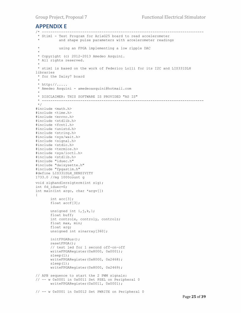
APPENDIX E /* ----------------------------------------------------------------------------
* Stim1 - Test Program for AriaG25 board to read accelerometer
* and shape pulse parameters with accelerometer readings
* using an FPGA implementing a low ripple DAC
*
* Copyright (c) 2012-2013 Amedeo Asquini.
* All rights reserved.
*
* stim1 is based on the work of Federico Lolli for its I2C and LIS331DLH
libraries
* for the Daisy7 board
*
* http://.....
* Amedeo Asquini - [email protected]
*
* DISCLAIMER: THIS SOFTWARE IS PROVIDED "AS IS"
* ----------------------------------------------------------------------------
*/
#include <math.h>
#include <time.h>
#include <errno.h>
#include <stdlib.h>
#include <fcntl.h>
#include <unistd.h>
#include <string.h>
#include <sys/wait.h>
#include <signal.h>
#include <stdio.h>
#include <termios.h>
#include <sys/ioctl.h>
#include <stdlib.h>
#include "iduec.h"
#include "daisysette.h"
#include "fpgastim.h"
#define LIS331DLH_SENSIVITY
1733.0 //mg 1000count g
void sighandlersigterm(int sig);
int fd_iduec=0;
int main(int argc, char *argv[])
{
int acc[3];
float accf[3];
unsigned int i,j,k,l;
float buff;
int controlx, controly, controlz;
float max, min;
float arg;
unsigned int sinarray[360];
initFPGABus();
resetFPGA();
// test led for 1 second off-on-off
writeFPGARegister(0x8000, 0x0001);
sleep(1);
writeFPGARegister(0x8000, 0x2468);
sleep(1);
writeFPGARegister(0x8000, 0x2469);
// APB sequence to start the 2 PWM signals:
// -- w 0x0001 in 0x0011 Set PSEL on Peripheral 0
writeFPGARegister(0x0011, 0x0001);
// -- w 0x0001 in 0x0012 Set PWRITE on Peripheral 0

Group Project, Proposal 7 Functional Electrical Stimulator
Page 26 of 39
writeFPGARegister(0x0012, 0x0001);
// now writings on the APB registers
// -- w 0x0001 in 0x00 PRESCALE
writeAPB(0x0000, 0x0001);
// -- w 0x0100 in 0x04 PERIOD
writeAPB(0x0004, 0x0100);
// -- w onPWM0 in 0x14 DAC1 LevelOut set
writeAPB(0x0014, 0x0);
// -- w onPWM1 in 0x1C DAC2 LevelOut set
writeAPB(0x001C, 0x0);
// -- w 0x0003 in 0x08 PWM Enable channel 1 and 2
writeAPB(0x0008, 0x0003);
// first write to PWM register so after we can just call writeAPBdata
// writeAPB(0x0014, 0x0); // channel 1 J1:6
writeAPB(0x001C, 0x0); // channel 2 J1:8
/*apertura i2c*/
fd_iduec=openi2c();
set_d7_initialize(fd_iduec);
/*collego il segnale di terminazione*/
signal(SIGTERM,sighandlersigterm);
printf("\n\nTest Accelerometer Daisy 7 - Amedeo Asquini Imperial
College London\n");
sleep(1);
/*main loop*/
printf("START!\n");
max = min = 0.0;
while (1) {
read_lis331dlh(fd_iduec ,acc);
// printf("Acc: x= %5.2f; y= %5.2f; z= %5.2f\n",accf[0],accf[1],
accf[2]); // controlx used to modulate the height of the pulse PWM// controly used to modulate the width of the pulse PWM
controlx = 0x8000 + acc[0]*2;
if (controlx<0) controlx = 0;
if (controlx>65500) controlx = 65500;
controly = (acc[1]<<1);
if (controly<-10000) controly = -10000;
// if (controly>200000) controly = 200000;
// if (acc[0] > max) max = acc[0];
// if (acc[0] < min) min = acc[0];
// printf("acc[0] = %12d accf[0] = %6.4f controlx = %8.3f min = %8.3f
max = %8.3f\n", acc[0], accf[0], controlx, min, max);
}
writeAPBdata((unsigned int)controlx);
mynanosleep(20001+controly);
writeAPBdata(0x0000);
mynanosleep(3000);
}//end main loop
closeFPGABus();
closei2c(fd_iduec);
return 0;
}
/*signal*/
void sighandlersigterm(int sig)
{
closei2c(fd_iduec);
exit(1);
}

Group Project, Proposal 7 Functional Electrical Stimulator
Page 27 of 39
APPENDIX F /* ----------------------------------------------------------------------------
* Pulse3 - Test Program for AriaG25 board to send shaped pulses
* using an FPGA implementing a low ripple DAC
*
* Copyright (c) 2012-2013 Amedeo Asquini.
* All rights reserved.
*
* Pulse3 is based on the work of Douglas Gilbert for its mem2io.c
* for accessing input output register of the CPU from userspace
*
* http://.....
* Amedeo Asquini - [email protected]
*
* DISCLAIMER: THIS SOFTWARE IS PROVIDED "AS IS" IN THE SAME
* TERMS OF THE ORIGINAL DISCLAIMER LISTED BELOW.
* ----------------------------------------------------------------------------
*/
/*
* Copyright (c) 2010-2012 Douglas Gilbert.
* All rights reserved.
*
* Redistribution and use in source and binary forms, with or without
* modification, are permitted provided that the following conditions
* are met:
* 1. Redistributions of source code must retain the above copyright
* notice, this list of conditions and the following disclaimer.
* 2. Redistributions in binary form must reproduce the above copyright
* notice, this list of conditions and the following disclaimer in the
* documentation and/or other materials provided with the distribution. * 3. The name of the author may not be used to endorse or promote products
* derived from this software without specific prior written permission. *
* THIS SOFTWARE IS PROVIDED BY THE AUTHOR AND CONTRIBUTORS ``AS IS'' AND
* ANY EXPRESS OR IMPLIED WARRANTIES, INCLUDING, BUT NOT LIMITED TO, THE
* IMPLIED WARRANTIES OF MERCHANTABILITY AND FITNESS FOR A PARTICULAR PURPOSE
* ARE DISCLAIMED. IN NO EVENT SHALL THE AUTHOR OR CONTRIBUTORS BE LIABLE
* FOR ANY DIRECT, INDIRECT, INCIDENTAL, SPECIAL, EXEMPLARY, OR CONSEQUENTIAL
* DAMAGES (INCLUDING, BUT NOT LIMITED TO, PROCUREMENT OF SUBSTITUTE GOODS
* OR SERVICES; LOSS OF USE, DATA, OR PROFITS; OR BUSINESS INTERRUPTION)
* HOWEVER CAUSED AND ON ANY THEORY OF LIABILITY, WHETHER IN CONTRACT, STRICT
* LIABILITY, OR TORT (INCLUDING NEGLIGENCE OR OTHERWISE) ARISING IN ANY WAY
* OUT OF THE USE OF THIS SOFTWARE, EVEN IF ADVISED OF THE POSSIBILITY OF
* SUCH DAMAGE.
*
*/
#include <stdio.h>
#include <stdlib.h>
#include <ctype.h>
#include <string.h>
#include <unistd.h>
#include <sys/mman.h>
#include <sys/types.h>
#include <sys/stat.h>
#include <fcntl.h>
#include <errno.h>
#include <time.h>
#include <math.h>
#define DEV_MEM "/dev/mem"
#define MAP_SIZE 4096 /* needs to be a power of 2! */
#define MAP_MASK (MAP_SIZE - 1)
#define PIOC_OER 0xfffff810 // (Wr) PIO Output Enable Register -> 1 to the
bit that has to be put in output
#define PIOC_ODR 0xfffff814 // (Wr) PIO Output Disable Register -> 1 to the
bit that has to be put in input

Group Project, Proposal 7 Functional Electrical Stimulator
Page 28 of 39
#define PIOC_SODR 0xfffff830 // (Wr) PIO Set Output Data Register -> 1 to the
output bitthat has to be set
#define PIOC_CODR 0xfffff834 // (Wr) PIO Clear Output Data Register -> 1 to
the output bit that has to be cleared
#define PIOC_ODSR 0xfffff838 // (Rd) PIO Output Data Status Register : to read
the output status of the PortC pins
#define PIOC_PDSR 0xfffff83C // (Rd) PIO Pin Data Status Register _ to read
the status of the PortC input pins
int mem_fd;
void * mmap_ptr;
int verbose = 0;
int isRead = 1;
int isWrite = 1;
off_t mask_addr;
void * mapped_PIOC_OER_addr;
void * mapped_PIOC_ODR_addr;
void * mapped_PIOC_SODR_addr;
void * mapped_PIOC_CODR_addr;
void * mapped_PIOC_ODSR_addr;
void * mapped_PIOC_PDSR_addr;
void mynanosleep(unsigned int cycles) {
// to be used to develop very small delays
int i;
volatile k,l=0;
for (i=0; i<cycles; i++) {
k=l;
}
}
init_memoryToIO(void) {
// to map in a local page the peripheral addresses used
mem_fd = -1;
if ((mem_fd = open(DEV_MEM, O_RDWR | O_SYNC)) < 0) {
printf("open of " DEV_MEM " failed");
return 1;
} else
if (verbose) printf("open(" DEV_MEM "O_RDWR | O_SYNC) okay\n");
mask_addr = (PIOC_OER & ~MAP_MASK); // preparation of mask_addr (base
of the memory accessed)
if (verbose) printf ("Mask address = %08x\n",mask_addr);
mmap_ptr = (void *)-1;
mmap_ptr = mmap(0, MAP_SIZE, PROT_READ | PROT_WRITE,
MAP_SHARED, mem_fd, mask_addr);
if (verbose) printf ("Mmap_ptr = %08x\n",mmap_ptr);
if ((void *)-1 == mmap_ptr) {
printf("addr=0x%x, mask_addr=0x%lx :\n", PIOC_OER,
mask_addr);
printf(" mmap");
return 1;
} else
}
if (verbose) printf("mmap() ok, mask_addr=0x%lx, mmap_ptr=%p\n",
mask_addr, mmap_ptr);
mapped_PIOC_OER_addr = mmap_ptr + (PIOC_OER & MAP_MASK);
mapped_PIOC_ODR_addr = mmap_ptr + (PIOC_ODR & MAP_MASK);
mapped_PIOC_SODR_addr = mmap_ptr + (PIOC_SODR & MAP_MASK);
mapped_PIOC_CODR_addr = mmap_ptr + (PIOC_CODR & MAP_MASK);
mapped_PIOC_ODSR_addr = mmap_ptr + (PIOC_ODSR & MAP_MASK);
mapped_PIOC_PDSR_addr = mmap_ptr + (PIOC_PDSR & MAP_MASK);
return 0;

Group Project, Proposal 7 Functional Electrical Stimulator
Page 29 of 39
close_memoryToIO(void) {
// closing mmap
if (-1 == munmap(mmap_ptr, MAP_SIZE)) {
printf("mmap_ptr=%p:\n", mmap_ptr);
printf(" munmap");
return 1;
} else if (verbose) printf("call of munmap() ok, mmap_ptr=%p\n", mmap_ptr);
if (mem_fd >= 0)
close(mem_fd);
return 0;
}
void initFPGABus(void) {
// not working yet.
// Bus has to be initialized from Python test program initBus.py
// based on the APB_BUS preliminary specification ... TBD
// put PC2..PC26 in output all in logic zero state (so also reset of the
FPGA)
// writes all zeroes on the data and control bus lines of the APB_Bone
in the FPGA
*((unsigned long *)mapped_PIOC_CODR_addr) = 0x07ffffc0;
mynanosleep(100000);
// put dat and control bus lines in output mode
*((unsigned long *)mapped_PIOC_OER_addr) = 0x07ffffC0;
}
mynanosleep(100000);
void resetFPGA(void) {
void * ap;
// resets the FPGA with a negative pulse on PC2
// lower and raise RESETN (PC2)
*((unsigned long *)mapped_PIOC_CODR_addr) = 0x00000004;
mynanosleep(100000);
*((unsigned long *)mapped_PIOC_SODR_addr) = 0x00000004;
mynanosleep(100000);
}
unsigned int readRegister(unsigned int reg) {
// returns the content of the CPU register reg
void * ap;
unsigned long ul;
ap = mmap_ptr + (reg & MAP_MASK);
// read the register
ul = *((unsigned long *)ap);
if (verbose) printf("read: addr=0x%x, val=0x%x\n", reg, (unsigned
int)ul);
}
return (unsigned int)ul;
#if 0
unsigned int readBusoutbits(void) {
// returns the content of the register reg
unsigned long ul;
}
// read the register
ul = *((unsigned long *)mapped_PIOC_ODSR_addr);
if (verbose) printf("read: addr=0x%x, val=0x%x\n", PIOC_PDSR, (unsigned
int)ul);
return (unsigned int)ul;
unsigned int readBusinbits(void) {
// returns the content of the register reg
unsigned long ul;
// read the register
ul = *((unsigned long *)mapped_PIOC_PDSR_addr);
if (verbose) printf("read: addr=0x%x, val=0x%x\n", PIOC_PDSR, (unsigned
int)ul);

Group Project, Proposal 7 Functional Electrical Stimulator
Page 30 of 39
return (unsigned int)ul;
#endif
}
void writeBus(unsigned int data) {
// write the output registers of Port C with the value "data"
*((unsigned long *)mapped_PIOC_SODR_addr) = data<<8;
*((unsigned long *)mapped_PIOC_CODR_addr) = (~data)<<8&0x00ffff00;
}
unsigned int readFPGARegister(unsigned int reg) {
void * ap;
unsigned long ul;
// writes in the Address Register of the APB_Bone in the FPGA
*((unsigned long *)mapped_PIOC_SODR_addr) = reg<<8;
*((unsigned long *)mapped_PIOC_CODR_addr) = ((~reg)<<8)&0x00ffff00;
// raise and lower the ADDRESS_WRITE line (PC24)
*((unsigned long *)mapped_PIOC_SODR_addr) = 0x01000000;
*((unsigned long *)mapped_PIOC_CODR_addr) = 0x01000000;
// put bus in input mode
*((unsigned long *)mapped_PIOC_ODR_addr) = 0x00ffff00;
// raise DATA_READ line (PC26)
*((unsigned long *)mapped_PIOC_SODR_addr) = 0x04000000;
// read the inbits
ul = *((unsigned long *)mapped_PIOC_PDSR_addr);
if (verbose) printf("read: addr=0x%x, val=0x%x\n", PIOC_PDSR, (unsigned
int)ul);
// lower DATA_READ line (PC26)
*((unsigned long *)mapped_PIOC_CODR_addr) = 0x04000000;
// put bus in output mode
*((unsigned long *)mapped_PIOC_OER_addr) = 0x00ffff00;
}
return (unsigned int)((ul&0x00ffff00)>>8);
void writeFPGARegister(unsigned int reg, unsigned int data) {
void * ap;
unsigned long ul;
// writes in the Address Register of the APB_Bone in the FPGA
*((unsigned long *)mapped_PIOC_SODR_addr) = reg<<8;
*((unsigned long *)mapped_PIOC_CODR_addr) = ((~reg)<<8)&0x00ffff00;
// raise and lower the ADDRESS_WRITE line (PC24)
*((unsigned long *)mapped_PIOC_SODR_addr) = 0x01000000;
*((unsigned long *)mapped_PIOC_CODR_addr) = 0x01000000;
// writes on the bus of the APB_Bone in the FPGA
*((unsigned long *)mapped_PIOC_SODR_addr) = data<<8;
*((unsigned long *)mapped_PIOC_CODR_addr) = ((~data)<<8)&0x00ffff00;
// raise and lower DATA_WRITE line (PC25)
*((unsigned long *)mapped_PIOC_SODR_addr) = 0x02000000;
*((unsigned long *)mapped_PIOC_CODR_addr) = 0x02000000;
}
void fastwriteFPGARegister(unsigned int reg, unsigned int data) {
void * ap;
unsigned long ul;
// continues to write on the same address register fo fast update of
values
// writes on the bus of the APB_Bone in the FPGA
*((unsigned long *)mapped_PIOC_SODR_addr) = data<<8;
*((unsigned long *)mapped_PIOC_CODR_addr) = ((~data)<<8)&0x00ffff00;
// raise and lower DATA_WRITE line (PC25)
*((unsigned long *)mapped_PIOC_SODR_addr) = 0x02000000;
*((unsigned long *)mapped_PIOC_CODR_addr) = 0x02000000;
}
void writeAPBdata(unsigned int data) {
// continues to write on the same APB register of fast update of values

Group Project, Proposal 7 Functional Electrical Stimulator
Page 31 of 39
// writes on the bus of the APB_Bone in the FPGA
*((unsigned long *)mapped_PIOC_SODR_addr) = data<<8;
*((unsigned long *)mapped_PIOC_CODR_addr) = ((~data)<<8)&0x00ffff00;
// raise and lower PENABLE line (PC3)
*((unsigned long *)mapped_PIOC_SODR_addr) = 0x00000008;
*((unsigned long *)mapped_PIOC_CODR_addr) = 0x00000008;
}
void writeAPB(unsigned int addr, unsigned int data) {
writeFPGARegister(0x0010, addr);
register to be written
writeAPBdata(data);
}
int main(int argc, char * argv[])
{
unsigned int i,j,k,l;
float buff;
float arg;
unsigned int sinarray[360];
unsigned int onPWM0 = 0x4000;
unsigned int onPWM1 = 0xd000;
float dutyPWM0, voltagePWM0;
float dutyPWM1, voltagePWM1;
unsigned int myreadregisterData;
// i = 0x1234;
// j = ~i;
// printf ("i= %08x j=%08x\n",i,j); if (init_memoryToIO()) {
printf ("Error in init_memoryToIO() \n");
}
return 1;
initFPGABus();
resetFPGA();
// test led for 1 second off-on-off
writeFPGARegister(0x8000, 0x0001);
sleep(1);
writeFPGARegister(0x8000, 0x2468);
sleep(1);
writeFPGARegister(0x8000, 0x2469);
// APB sequence to start the 2 PWM signals:
// -- w 0x0001 in 0x0011 Set PSEL on Peripheral 0
writeFPGARegister(0x0011, 0x0001);
// -- w 0x0001 in 0x0012 Set PWRITE on Peripheral 0
writeFPGARegister(0x0012, 0x0001);
// now writings on the APB registers
// -- w 0x0001 in 0x00 PRESCALE
writeAPB(0x0000, 0x0001);
// -- w 0x0100 in 0x04 PERIOD
writeAPB(0x0004, 0x0100);
// -- w onPWM0 in 0x14 DAC1 LevelOut set
writeAPB(0x0014, 0x0);
// -- w onPWM1 in 0x1C DAC2 LevelOut set
writeAPB(0x001C, 0x0);
// -- w 0x0003 in 0x08 PWM Enable channel 1 and 2
writeAPB(0x0008, 0x0003);
// first write to PWM register so after we can just call writeAPBdata
writeAPB(0x0014, 0x0); // writeAPB(0x001C, 0x0);
#if 0
printf("Pulse1 program rel 1.0\n");
//# write APB register pointer (0x10) with the APB
printf("Sawtooth enveloped pulses of 10us high and spaced 60us\n");
printf("START 10000 bursts! ...\n");

Group Project, Proposal 7 Functional Electrical Stimulator
Page 32 of 39
for(j=0; j<10000; j++) {
if (j%1000 == 0) printf ("j=%d\n");
for (k=0; k<16; k++) {
writeAPBdata(k<<12);
mynanosleep(200);
writeAPBdata(0x0000);
mynanosleep(1500);
}
} printf("STOP! \n");
#endif
#if 1
printf("Pulse2 program rel 1.0\n");
printf("Continuous sin and -sin output at 16kHz 16 bit. 1.7Msamples/s\n");
for (k=0; k<180; k++) {
buff = sin ((k<<1)*3.14159/180.0) + 1;
sinarray[k] = (unsigned int)(32000*buff)&0xffff;
}
for (k=0; k<180; k++) {
buff = -sin ((k<<1)*3.14159/180.0) + 1;
sinarray[k+180] = (unsigned int)(32000*buff)&0xffff;
}
for(j=0; j<10000; j++) {
if (j%1000 == 0) printf ("j=%d\n");
for (k=0; k<360; k++) {
writeAPBdata(sinarray[k]);
}
}
#endif
#if 1
printf("Pulse3 program rel 1.0\n");
printf("Shaped sin-sin pulses 100us wide\n");
for (k=0; k<90; k++) {
buff = 2.5+0.5*sin ((k<<2)*3.14159/180.0);
sinarray[k] = (unsigned int)(20000*buff)&0xffff;
}
for(j=0; j<100000; j++) {
if (j%1000 == 0) printf ("j=%d\n");
for (k=0; k<90; k++) {
if (j%1000 == 0) printf ("j=%d\n");
for (k=0; k<90; k++) { writeAPBdata(sinarray[k]);
}
writeAPBdata(0x0);
mynanosleep(3000);
}
#endif
if (close_memoryToIO()) {
printf ("Error in close_memoryToIO() \n");
return 1;
}
}

Group Project, Proposal 7 Functional Electrical Stimulator
Page 33 of 39
APPENDIX G
Figure 4: Shows internal architecture of the FPGA design using Microsemi Libero 9.1
For more details on the operation of the low ripple DAC mode and the PWM core, please visit http://www.actel.com/ipdocs/CorePWM_HB.pdf
For details on the operation of the PLL, please visit
http://www.actel.com/documents/gen_refguide_ide_ug.pdf (page 147).
The VHDL code for the interface logic between the Linux embedded board and the FPGA is
reported below:
-- APB_Bone_0_91.vhd
-- based on the Fox_Bone protocol from Acme Systems srl (www.acmesystems.it)
library ieee;
use ieee.std_logic_1164.all;
use ieee.std_logic_unsigned.all;
library proasic3;
-- The 16 bit registers enabled in this APB_Bone Sample code are:
-- 0x0004: readable register returning the APB_Bone release (presently 0x0080 or 0.8.0)
-- 0x0005: first hardware application word returning 0x0001 (Link Establishment)
-- 0x0006: second hardware application word returning 0x0001 (stands for example 1)
-- 0x0007: third hardware application word TBD for now returning zeroes.
-- 0x8000: read/write general register (for testing of external interfacing with the
Bone)
-- bit 0 register 0x8000 connected with output E3 on the FPGA to monitor with the
LED the connection
-- APB specific registers:
-- 0x0010: APB ADDRESS register (write here to store the address of the APB peripheral
-- register you need to write to
-- 0x0011: APB PERIPHERAL SELECT register (up to 16 APB peripherals PSEL selectable, also
in broadcast)
-- a '1' on more than one bit in this register will select more than one APB
peripheral to write
-- 0x0012: APB PERIPHERAL WRITE register (up to 16 APB peripherals PWRITE selectable)
-- 0x0020: APB_0_PRDATA register to be able to read back APB peripheral 0 addressed
register
-- connect to the PRDATA lines of the APB peripheral 0
entity APB_Bone is

Group Project, Proposal 7 Functional Electrical Stimulator
Page 34 of 39
port(-- APB_Bone Interface signals
HOST_BUS : inout std_logic_vector(15 downto 0); -- Host bus input/output lines.
ADDRESS_WRITE : in std_logic; -- to strobe the actual register address to be
used.
DATA_WRITE : in std_logic; -- to strobe the actual data in the previously
addressed register.
DATA_READ : in std_logic; -- to enable the addressed APB register of the
selected APB
-- peripheral to drive the APB_Bone data lines
-- as to be read from the Fox Board software
RESETN : in std_logic; -- active low
APB_ADDRESS_BUS : out std_logic_vector(7 downto 0);
APB_PERIPHERALSELECT : out std_logic_vector(15 downto 0);
APB_PERIPHERALWRITE : out std_logic_vector(15 downto 0);
APB_PRDATA : in std_logic_vector(15 downto 0);
APB_WRDATA : out std_logic_vector(15 downto 0);
APB_LED : out std_logic
);
end APB_Bone;
architecture Behavioral of APB_Bone is
-- declaration of some constants used as names for the FoxBone registers and their
fixed value (if applicable).
constant RELEASE_REGISTER_0_ADDRESS : std_logic_vector := x"0004";
constant RELEASE_REGISTER_1_ADDRESS : std_logic_vector := x"0005";
constant RELEASE_REGISTER_2_ADDRESS : std_logic_vector := x"0006";
constant RELEASE_REGISTER_3_ADDRESS : std_logic_vector := x"0007";
-- here declared the constants acting as fixed value registers.
constant RELEASE_REGISTER_0_VALUE : std_logic_vector := x"0091";
constant RELEASE_REGISTER_1_VALUE : std_logic_vector := x"0001";
constant RELEASE_REGISTER_2_VALUE : std_logic_vector := x"0001";
constant RELEASE_REGISTER_3_VALUE : std_logic_vector := x"0000";
-- here are the general registers address name definition (normally they are more
application specific)
constant GENERAL_REGISTER_8000_ADDRESS : std_logic_vector := x"8000";
constant APB_ADDRESS_REGISTER_ADDRESS : std_logic_vector := x"0010";
constant APB_PERIPHERALSELECT_REGISTER_ADDRESS : std_logic_vector := x"0011";
constant APB_PERIPHERALWRITE_REGISTER_ADDRESS : std_logic_vector := x"0012";
constant APB_0_PRDATA_ADDRESS : std_logic_vector := x"0020";
-- internal signals (going between components)
signal Address : std_logic_vector (15 downto 0); -- declaration of the internal signals
lines realizing the FoxBone address register.
-- register declaration (as a internal signal) for the general register at address
8000h
signal Register8000 : std_logic_vector(15 downto 0) := x"0000";
signal APB_ADDRESS_Reg : std_logic_vector(15 downto 0);
signal APB_PERIPHERALSELECT_Reg : std_logic_vector(15 downto 0);
signal APB_PERIPHERALWRITE_Reg : std_logic_vector(15 downto 0);
signal APB_0_PRDATA : std_logic_vector(15 downto 0);
-- here are the interconnections, the functional logic code blocks and the instantiation
of all the
-- required components of this VHDL source code file.
begin
-- this is the implementation of the FoxBone address register:
Address <= (others => '0') when RESETN = '0' else
HOST_BUS when ADDRESS_WRITE = '1';
-------------------------------------------
-- input from release registers
HOST_BUS <= RELEASE_REGISTER_0_VALUE when Address = RELEASE_REGISTER_0_ADDRESS and
DATA_READ = '1' else
(others=>'Z');
HOST_BUS <= RELEASE_REGISTER_1_VALUE when Address = RELEASE_REGISTER_1_ADDRESS and
DATA_READ = '1' else

Group Project, Proposal 7 Functional Electrical Stimulator
Page 35 of 39
(others=>'Z');
HOST_BUS <= RELEASE_REGISTER_2_VALUE when Address = RELEASE_REGISTER_2_ADDRESS and
DATA_READ = '1' else
(others=>'Z');
HOST_BUS <= RELEASE_REGISTER_3_VALUE when Address = RELEASE_REGISTER_3_ADDRESS and
DATA_READ = '1' else
(others=>'Z');
-------------------------------------------
-- implementation of a general register for read and write at address 8000 for
demonstration purposes
-- input from general register at 8000h
HOST_BUS <= Register8000 when Address = GENERAL_REGISTER_8000_ADDRESS and DATA_READ =
'1' else
(others=>'Z');
-- write operation to the general register at 8000h to set its value
Register8000 <= x"0000" when RESETN = '0' else
HOST_BUS when Address = GENERAL_REGISTER_8000_ADDRESS and DATA_WRITE
= '1';
APB_LED <= Register8000 (0);
-------------------------------------------
--APB section
APB_ADDRESS_BUS <= APB_ADDRESS_Reg (7 downto 0);
APB_0_PRDATA <= APB_PRDATA;
APB_WRDATA <= HOST_BUS;
APB_PERIPHERALSELECT <= APB_PERIPHERALSELECT_Reg;
APB_PERIPHERALWRITE <= APB_PERIPHERALWRITE_Reg;
-- input from APB_ADDRESS register
HOST_BUS <= APB_ADDRESS_Reg when Address = APB_ADDRESS_REGISTER_ADDRESS and DATA_READ =
'1' else
(others=>'Z');
-- write operation to the APB_ADDRESS register to set its value
APB_ADDRESS_Reg <= x"0000" when RESETN = '0' else
HOST_BUS when Address = APB_ADDRESS_REGISTER_ADDRESS and DATA_WRITE =
'1';
---
-- input from APB_PERIPHERALSELECT register
HOST_BUS <= APB_PERIPHERALSELECT_Reg when Address =
APB_PERIPHERALSELECT_REGISTER_ADDRESS and DATA_READ = '1' else
(others=>'Z');
-- write operation to the APB_PERIPHERALSELECT register to set its value
APB_PERIPHERALSELECT_Reg <= x"0000" when RESETN = '0' else
HOST_BUS when Address = APB_PERIPHERALSELECT_REGISTER_ADDRESS and
DATA_WRITE = '1';
---
-- input from APB_PERIPHERALWRITE register
HOST_BUS <= APB_PERIPHERALWRITE_Reg when Address = APB_PERIPHERALWRITE_REGISTER_ADDRESS
and DATA_READ = '1' else
(others=>'Z');
-- write operation to the APB_PERIPHERALWRITE register to set its value
APB_PERIPHERALWRITE_Reg <= x"0000" when RESETN = '0' else
HOST_BUS when Address = APB_PERIPHERALWRITE_REGISTER_ADDRESS and
DATA_WRITE = '1';
---
-- input from APB_0_PRDATA lines
HOST_BUS <= APB_0_PRDATA when Address = APB_0_PRDATA_ADDRESS and DATA_READ = '1' else
(others=>'Z');
end Behavioral;

Group Project, Proposal 7 Functional Electrical Stimulator
Page 36 of 39
APPENDIX H
Figure 5: Shows signal with higher ripple at high and low amplitudes
Figure 6: Shows arbitrary pulse waveform rise time and ripple

Group Project, Proposal 7 Functional Electrical Stimulator
Page 37 of 39
Figure 7: Shows magnified version of figure 7, highlighting the rise time

Group Project, Proposal 7 Functional Electrical Stimulator
Page 38 of 39
APPENDIX I
Figure 8: Schematic of circuit to interface with the electrodes

Group Project, Proposal 7 Functional Electrical Stimulator
Page 39 of 39
APPENDIX J
Table 3: Shows detailed breakdown of component costs (given in £)
†
quantity needed for 8 channels stimulator
††number in parentheses represents minimum number of components to avail this price
†††include resistors, capacitors, diodes, voltage regulators etc. Price provided is crude estimate
Table 4: Shows Initial costs that are incurred only once and production costs (given in £)
Start-Up costs
Medical Device Registration
Total cost Cost per
unit* Variable Fixed
Application of Designation
N/A 3850 3.85
Initial Designation Audit N/A 4670 4.67
Surveillance N/A 3840 3.84
Patents N/A 4000 4.00
Production costs
PCB manufacturing 1.20 364 1.56
Component mounting 0.02† 430 6.43
††
Encasing 1.00 4500 5.50
Total Additional Costs for First Year 29.85
Total Additional Costs Following Years 8.20
†Per component ††assuming 300 components per unit *Assuming 1000 unit sales