Stacking faults in WSi2: Resistivity effects
4
Stacking faults in WSi2: Resistivity effects F. M. d’Heurle, F. K. LeGoues, R. Joshi, and Ilka Suni Citation: Applied Physics Letters 48, 332 (1986); doi: 10.1063/1.96542 View online: http://dx.doi.org/10.1063/1.96542 View Table of Contents: http://scitation.aip.org/content/aip/journal/apl/48/5?ver=pdfcov Published by the AIP Publishing This article is copyrighted as indicated in the article. Reuse of AIP content is subject to the terms at: http://scitation.aip.org/termsconditions. Downloaded to IP: 142.134.145.190 On: Fri, 14 Mar 2014 08:19:44
Transcript of Stacking faults in WSi2: Resistivity effects
Stacking faults in WSi2: Resistivity effectsF. M. d’Heurle, F. K. LeGoues, R. Joshi, and Ilka Suni Citation: Applied Physics Letters 48, 332 (1986); doi: 10.1063/1.96542 View online: http://dx.doi.org/10.1063/1.96542 View Table of Contents: http://scitation.aip.org/content/aip/journal/apl/48/5?ver=pdfcov Published by the AIP Publishing
This article is copyrighted as indicated in the article. Reuse of AIP content is subject to the terms at: http://scitation.aip.org/termsconditions. Downloaded to IP:
142.134.145.190 On: Fri, 14 Mar 2014 08:19:44
Stacking faults in WSi2: Resistivity effects F. M. d'Heurle, F. K. LeGoues, and R. Joshi IBM Thomas 1. Watson Research Center, Yorktown Heights, New York /0598
IIka Suni Technical Research Center of Finland, Semiconductor Laboratory, Otakaari 7B, SF-02150, Espoo, Finland
(Received 5 September 1985; accepted for publication 4 December 1985)
Films ofWSi 2 initially deposited in an amorphous form have been known to display an unexpected resistivity maximum when annealed at a temperature corresponding to the transition from the low-temperature hexagonal structure to the high-temperature tetragonal structure. It is shown that the resistivity maximum is due to an extremely high (5 X 10⁶
/ cm) density of stacking faults. Thus, at least one of the scattering defects which contribute to the relatively high resistivity of WSi2 films has been identified.
The electrical transport properties of silicides, be it MoSi2, I or CoSi 2 and NiSi2
2 are the object of current investigations. From a practical point of view one is not only concerned with the intrinsic properties of these compounds but also with the various scattering mechanisms which prevent silicide films from reaching the maximum possible conductivity. To date relatively little is known about these mechanisms. The experimentally established correlation between a decreasing resistivity and an increasing grain size has led to the generally accepted (although partly faulty) conclusion that grain boundaries are the main scatterers in annealed silicide films. However, it has been noted} that the magnitude of the resistivity effects is incompatible with a valid model4 for grain boundary scattering; other scattering centers must be operative. In the case of the silicides such as WSi2 (and possibly also TaSi2 and TiSU it is thought that the stacking faults should playa significant role in determining the resistivity, although there has been no other report or mention of stacking faults in these silicides. Such planar defects in metals were the object of great interest many years ago, especially in face-centered-cubic materials (Cu and alpha brass), 5 and in Co (Ref. 6) which undergoes a transition from hexagonal to cubic symmetry at about 400 dc. Some attention has been paid to stacking faults in compounds,7 especially in materials with the wurtzite and zincblend structure,8 binary compounds with the same stacking orders as the two forms of Co. One recent pUblication9 shows that interest in stacking faults remains very much alive.
Crystalline WSi2 is constituted of stoichiometric planes of atoms with an hexagonal symmetry where each W is surrounded by six Si atoms, very similar to Cu3Au, or to Co (if one ignores the identity of the two types of atoms). At low temperatures the stacking order of the hexagonal phase 10. I I
is ABeA, above a transition temperature in the vicinity of 550°C the structure becomes tetragonal with stacking order ABA. But for the fact that the coordination number is 10 in WSi2 and 12 in Co, the transitions of these two materials appear to be quite similar. At the transition temperature the free energy (but not the enthalpy) of the stacking faults should fall to zero, and their density should increase accordingly. An unexpected resistivity maximum II in WSi2 films annealed near the transition temperature has been attributed to a presumed high resistivity of the hexagonal phase. How-
ever, this is suspicious for two reasons: (a) the atomic structures of the two phases are identical; (b) the isomorphous TaSi2 has a resistivity even lower than that of tetragonal WSi2 . For Co at 700 K the resistivity changes for 24.5 for the cubic form to 26.3 f-lO cm for the hexagonal form.12 It is more likely that the excess resistivity observed in WSi2,
amounting to some 100 f-lO cm, is due to stacking faults. The transition temperature referred to here, 550°C, is
rather poorly defined. Tungsten disilicide has a melting point close to 2500 DC; it is known3 that whereas the Si atoms become readily mobile at about 700 DC, a similar mobility of the metal atoms requires temperatures of the order of 1100 dc. Thus 550°C constitutes a very low temperature for such a material, making the transition extremely sluggish, and the exact determination of the true thermodynamic transition temperature extremely difficult; one can only say that the transition temperature appears to be 550 dc. As a matter of fact the transition temperature is so low that the transition is found to be experimentally irreversible, but this is not thought to affect its thermodynamic character- Perhaps this point need not be finally settled here: a high density of stacking faults is anticipated regardless of whether the transition is an equilibrium phenomenon or not. The transport properties of well annealed WSi2 have been analyzed quite thoroughly. 14,15
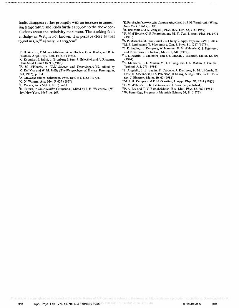
The results below were obtained with a film prepared initially in an amorphous condition by chemical vapor deposition from the reaction ofWF6 and SiH4 . The thickness was determined by Rutherford backscattering to be about 74 nm [from the number of Watoms per square centimeter, assuming (a) a stoichiometric composition and (b) an atomic density corresponding exactly to the unit cell for tetragonal WSi2 ]. The composition is known to correspond to a W -Si ratio close to 30-70. The films were annealed for 1 h at different temperatures in He purified both over hot Ti and hot ZrThe resistivity (measured by means of a four-point probe) is listed as a function of the annealing temperature in Table I. A series of x-ray diffraction patterns (eu Ka ) obtained with several of these samples is displayed in Fig. 1. The pattern for a sample annealed at 1000 °e shows distinctly those peaks belonging to the tetragonal structure. The other peaks belong to the hexagonal structure_ At least one broad peak at about 11 ° belongs to both structures.
332 Appl. Phys. Lett. 48 (5), 3 February 1986 0003-6951/86/050332-03$01.00 ~. 1986 American Institute of Physics 332
This article is copyrighted as indicated in the article. Reuse of AIP content is subject to the terms at: http://scitation.aip.org/termsconditions. Downloaded to IP:
142.134.145.190 On: Fri, 14 Mar 2014 08:19:44
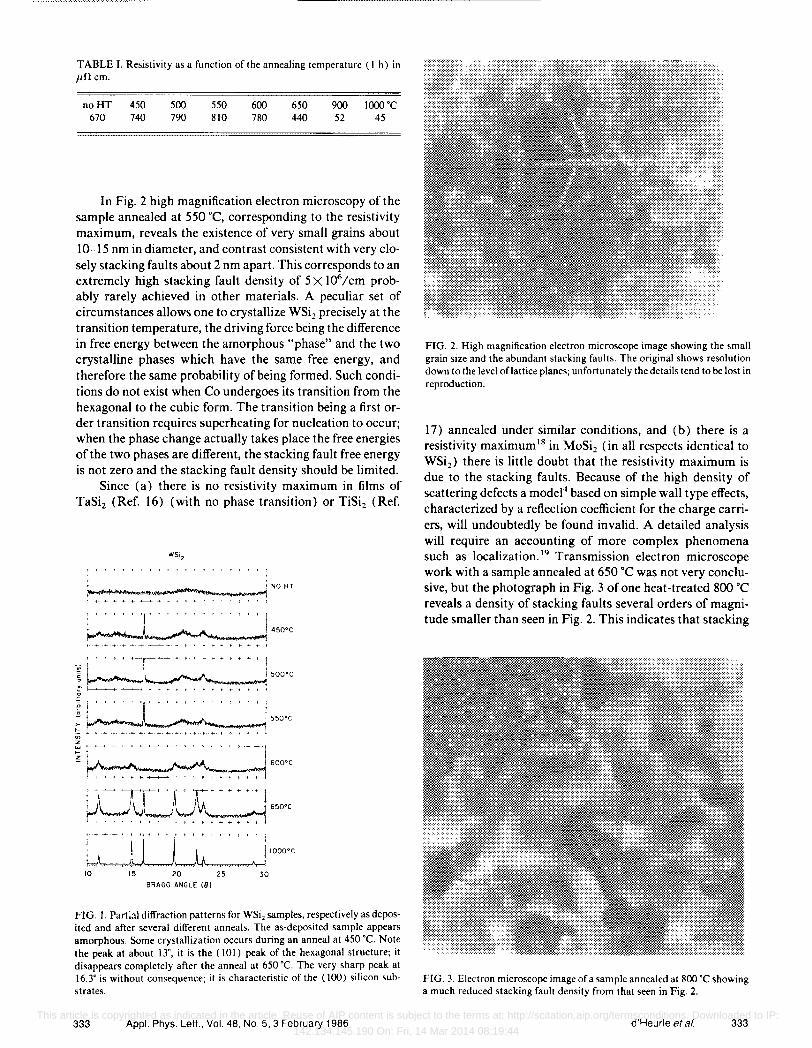
TABLE I. Resistivity as a function of the annealing temperature (I h) in flU em.
no HT 450 670 740
500 790
550 8\0
600 780
650 440
900 lOOOT 52 45
In Fig. 2 high magnification electron microscopy of the sample annealed at 550 ·C, corresponding to the resistivity maximum, reveals the existence of very small grains about 10-15 nm in diameter, and contrast consistent with very closely stacking faults about 2 nm apart. This corresponds to an extremely high stacking fault density of 5 X 10⁶ fcm probably rarely achieved in other materials. A peculiar set of circumstances allows one to crystallize WSi2 precisely at the transition temperature, the driving force being the difference in free energy between the amorphous "phase" and the two crystalline phases which have the same free energy, and therefore the same probability of being formed. Such conditions do not exist when Co undergoes its transition from the hexagonal to the cubic form. The transition being a first order transition requires superheating for nucleation to occur; when the phase change actually takes place the free energies of the two phases are different, the stacking fault free energy is not zero and the stacking fault density should be limited.
Since (a) there is no resistivity maximum in films of TaSi2 (Ref. 16) (with no phase transition) or TiSi2 (Ref.
;···'~T·-··-·-···-·'I
~~450'C
_ ; • , ~ • ~-+If-'-+---+ ..... I- +- .. ~ .. + t i ... t I I
~~~500'C ~~-"'-------+--t"+-j •• " ••• >.--t .. t~
~ i +- t- .. ~ T+ ... f • t • I L, T
~~~550'C z Wi-+----+-t +- + .. +----+ ... >.- .. ~ ~ •• L , >.- ~.
I- , , z I j
- lA........w.A. ....~ t 600'C
C-~~'.-.~.:-.. ~ ; ., ~ AT' , .. T-' .... , j ~Y.~~~)~~ 650'C
! . + ~, I r-' + I " + ' ••• , • llooo'c f-f~~~ 10 15 20 25 30
BRAGG ANGLE e81
FIG. I. Part;::1 diffraction patterns for WSi, samples, respectively as deposited and after several different anneals. The as-deposited sample appears amorphous. Some crystallization occurs during an anneal at 450·C. Note the peak at about 13', it is the (101) peak of the hexagonal structure; it disappears completely after the anneal at 650°C. The very sharp peak at 16.3° is without consequence; it is characteristic of the (100) silicon substrates.
333 Appl. Phys. Lett., Vol. 48, No 5, 3 February 1986
FIG. 2. High magnification electron microscope image showing the small grain size and the abundant stacking faults. The original shows resolution down to the level oflattice planes; unfortunately the details tend to be lost in reproduction.
17) annealed under similar conditions, and (b) there is a resistivity maximum 18 in MoSi2 (in all respects identical to WSi2 ) there is little doubt that the resistivity maximum is due to the stacking faults. Because of the high density of scattering defects a model4 based on simple wall type effects, characterized by a reflection coefficient for the charge carriers, will undoubtedly be found invalid. A detailed analysis will require an accounting of more complex phenomena such as localization. 19 Transmission electron microscope work with a sample annealed at 650·C was not very conclusive, but the photograph in Fig. 3 of one heat-treated 800 DC reveals a density of stacking faults several orders of magnitude smaller than seen in Fig. 2. This indicates that stacking
FIG. 3. Electron microscope image ofa sample annealed at 800'C showing a much reduced stacking fault density from that seen in Fig. 2.
d'Heurle et al. 333 This article is copyrighted as indicated in the article. Reuse of AIP content is subject to the terms at: http://scitation.aip.org/termsconditions. Downloaded to IP:
142.134.145.190 On: Fri, 14 Mar 2014 08:19:44
faults disappear rather promptly with an increase in annealing temperature and lends further support to the above conclusions about the resistivity maximum. The stacking fault enthalpy in WSi2 is not known; it is perhaps close to that found in CO,20 namely, 20 ergs/cm2.
'P. H. Woerlee, P. M. van Attekum, A. A. Hoeben, G. A. Hurks, and R. A. Wolters, App!. Phys. Lett. 44, 876 (1984).
2c. Krontiras, J. Salmi, L. Gronberg, I. Suni, J. He1eskivi, and A. Rissanen, Thin Solid Films 125, 93 (1985).
'F. M. d'Heurle, in VLSI Science and Technology/1982, edited by C. DelI'Oca and W. M. Bullis (The Electrochemical Society, Pennington, NJ, 1982), p. 194.
4A. Mayadas and M. Schatzkes, Phys. Rev. B 1,1382 (1970). 'c. N. Wagner, Acta Met. 5, 427 (1957). 6E. Votava, Acta Met. 8, 901 (1960). 'N. Brown, in Intermetallic Compounds, edited by J. H. Westbrook (Wiley, Ncow York, 1967), p. 265.
334 Appl. Phys Lett., Vol. 48, No.5, 3 February 1986
"E. Parthe, in Intermetallic Compounds, edited by J. H. Westbrook (Wiley, New York, 1967), p. 180.
OR. Bruinsma and A. Zangwill, Phys. Rev. Lett. 55, 214 ( 1985). !OF. M. d'Heurle, C. S. Petersson, and M. Y. Tsai, J. App!. Phys. 51, 5976
(1981 ). "s. P. Murarka, M. Read, and C. C. Chang, J. App!. Phys. 52, 7450 ( 1981). '2M. J. Laubitz and T. Matsumura, Can. J. Phys. 51, 1247 (1973). "]. E. Baglin, J. J. Dempsey, W. Hammer, F. M. d'Heurle, C. S. Petersson,
and C. Serrano, J. Electron, Mater. 8, 641 (1979). '·T. L. Martin, V. Malhotra, and J. E. Mahan, J. Electron. Mater. 13, 309
(1984). "V. Malhotra, T. L. Martin, M. T. Huang, and J. E. Mahan, J. Vac. Sci.
Techno!. A 2,271 (1984). '"J. Angilello, J. E. Baglin, F. Cardone, J. Dempsey, F. M. d'Heurle, E.
Irene, R. MacInness, C. S. Petersson, R. Savoy, A. Segmuller, and E. Tierney, J. Electron, Mater. 10,60 (1981).
17M. J. H. Kemper and P. H. Ooosting, J. App!. Phys. 53, 6214 (1982). '"F. M. d'Heurle, F. K. LeGoues, and I. Suni, (unpublished). ,op. A. Lee and T. V. Ramakrishnan, Rev. Mod. Phys. 57, 287 (1985). 2GW. Betteridge, Progress in Materials Science 24, 51 (1979).
d'Heurle et al. 334
This article is copyrighted as indicated in the article. Reuse of AIP content is subject to the terms at: http://scitation.aip.org/termsconditions. Downloaded to IP:
142.134.145.190 On: Fri, 14 Mar 2014 08:19:44


![Characterization of individual stacking faults in a …...Investigation of the scanning electron microscopy (SEM) images [see Fig. 1(a)] shows that a pyramidal base is formed at the](https://static.fdocuments.in/doc/165x107/5fa1f165e6a1ba11b36f72fd/characterization-of-individual-stacking-faults-in-a-investigation-of-the-scanning.jpg)