Stable, single-photon emitter in a thin organic crystal...
13
Stable, single-photon emitter in a thin organic crystal for application to quantum-photonic devices Claudio Polisseni, 1 Kyle D. Major, 1 Sebastien Boissier, 1 Samuele Grandi, 1 Alex S. Clark, 1 and E. A. Hinds 1,* 1 Centre for Cold Matter, Blackett Laboratory, Imperial College London, London, SW7 2AZ, UK 2 [email protected] * [email protected] Abstract: Single dibenzoterrylene (DBT) molecules offer great promise as bright, reliable sources of single photons on demand, capable of integra- tion into solid-state devices. It has been proposed that DBT in anthracene might be placed close to an optical waveguide for this purpose, but so far there have been no demonstrations of sufficiently thin crystals, with a con- trolled concentration of the dopant molecules. Here we present a method for growing very thin anthracene crystals from super-saturated vapour, which produces crystals of extreme flatness and controlled thickness. We show how this crystal can be doped with an adjustable concentration of diben- zoterrylene (DBT) molecules and we examine the optical properties of these molecules to demonstrate their suitability as quantum emitters in nanopho- tonic devices. Our measurements show that the molecules are available in the crystal as single quantum emitters, with a well-defined polarisation rela- tive to the crystal axes, making them amenable to alignment with optical nanostructures. We find that the radiative lifetime and saturation intensity vary little within the crystal and are not in any way compromised by the unusual matrix environment. We show that a large fraction of these emitters can be excited more than 10 12 times without photo-bleaching, making them suitable for real applications. Published by The Optical Society under the terms of the Creative Commons Attribution 4.0 License. Further distribution of this work must maintain attribution to the author(s) and the published article’s title, journal citation, and DOI. OCIS codes: (160.4890) Organic materials; (180.1790) Confocal microscopy; (310.1860) De- position and fabrication; (270.5290) Photon statistics. References and links 1. J. L. O’Brien, “Optical quantum computing,” Science 318, 1567–1570 (2007). 2. Y. He, Y.-M. He, Y.-J. Wei, X. Jiang, M.-C. Chen, F.-L. Xiong, Y. Zhao, C. Schneider, M. Kamp, S. H¨ ofling, C.- Y. Lu, and J.-W. Pan, “Indistinguishable tunable single photons emitted by spin-flip raman transitions in InGaAs quantum dots,” Phys. Rev. Lett. 111, 237403 (2013). 3. C. Kurtsiefer, S. Mayer, P. Zarda, and H. Weinfurter, “Stable solid-state source of single photons,” Phys. Rev. Lett. 85, 290–293 (2000). 4. I. Aharonovich, A. D. Greentree, and S. Prawer, “Diamond photonics,” Nature Photon. 5, 397–405 (2011). 5. A. A. L. Nicolet, C. Hofmann, M. A. Kolchenko, B. Kozankiewicz, and M. Orrit, “Single dibenzoterrylene molecules in an anthracene crystal: Spectroscopy and photophysics,” Chem. Phys. Chem. 8, 1215–1220 (2007). 6. P. Tamarat, A. Maali, B. Lounis, and M. Orrit, “Ten years of single molecule spectroscopy,” J. Phys. Chem. A 104, 1–16 (2000). #256843 Received 6 Jan 2016; revised 26 Jan 2016; accepted 5 Feb 2016; published 4 Mar 2016 © 2016 OSA 7 Mar 2016 | Vol. 24, No. 5 | DOI:10.1364/OE.24.005615 | OPTICS EXPRESS 5615
Transcript of Stable, single-photon emitter in a thin organic crystal...

Stable, single-photon emitter in a thinorganic crystal for application to
quantum-photonic devices
Claudio Polisseni,1 Kyle D. Major,1 Sebastien Boissier,1 SamueleGrandi,1 Alex S. Clark,1 and E. A. Hinds1,∗
1Centre for Cold Matter, Blackett Laboratory, Imperial College London,London, SW7 2AZ, UK
[email protected]∗[email protected]
Abstract: Single dibenzoterrylene (DBT) molecules offer great promiseas bright, reliable sources of single photons on demand, capable of integra-tion into solid-state devices. It has been proposed that DBT in anthracenemight be placed close to an optical waveguide for this purpose, but so farthere have been no demonstrations of sufficiently thin crystals, with a con-trolled concentration of the dopant molecules. Here we present a method forgrowing very thin anthracene crystals from super-saturated vapour, whichproduces crystals of extreme flatness and controlled thickness. We showhow this crystal can be doped with an adjustable concentration of diben-zoterrylene (DBT) molecules and we examine the optical properties of thesemolecules to demonstrate their suitability as quantum emitters in nanopho-tonic devices. Our measurements show that the molecules are available inthe crystal as single quantum emitters, with a well-defined polarisation rela-tive to the crystal axes, making them amenable to alignment with opticalnanostructures. We find that the radiative lifetime and saturation intensityvary little within the crystal and are not in any way compromised by theunusual matrix environment. We show that a large fraction of these emitterscan be excited more than 1012 times without photo-bleaching, making themsuitable for real applications.Published by The Optical Society under the terms of the Creative Commons Attribution 4.0License. Further distribution of this work must maintain attribution to the author(s) and thepublished article’s title, journal citation, and DOI.OCIS codes: (160.4890) Organic materials; (180.1790) Confocal microscopy; (310.1860) De-position and fabrication; (270.5290) Photon statistics.
References and links1. J. L. O’Brien, “Optical quantum computing,” Science 318, 1567–1570 (2007).2. Y. He, Y.-M. He, Y.-J. Wei, X. Jiang, M.-C. Chen, F.-L. Xiong, Y. Zhao, C. Schneider, M. Kamp, S. Hofling, C.-
Y. Lu, and J.-W. Pan, “Indistinguishable tunable single photons emitted by spin-flip raman transitions in InGaAsquantum dots,” Phys. Rev. Lett. 111, 237403 (2013).
3. C. Kurtsiefer, S. Mayer, P. Zarda, and H. Weinfurter, “Stable solid-state source of single photons,” Phys. Rev.Lett. 85, 290–293 (2000).
4. I. Aharonovich, A. D. Greentree, and S. Prawer, “Diamond photonics,” Nature Photon. 5, 397–405 (2011).5. A. A. L. Nicolet, C. Hofmann, M. A. Kolchenko, B. Kozankiewicz, and M. Orrit, “Single dibenzoterrylene
molecules in an anthracene crystal: Spectroscopy and photophysics,” Chem. Phys. Chem. 8, 1215–1220 (2007).6. P. Tamarat, A. Maali, B. Lounis, and M. Orrit, “Ten years of single molecule spectroscopy,” J. Phys. Chem. A
104, 1–16 (2000).
#256843 Received 6 Jan 2016; revised 26 Jan 2016; accepted 5 Feb 2016; published 4 Mar 2016 © 2016 OSA 7 Mar 2016 | Vol. 24, No. 5 | DOI:10.1364/OE.24.005615 | OPTICS EXPRESS 5615

7. J.-B. Trebbia, H. Ruf, P. Tamarat, and B. Lounis, “Efficient generation of near infra-red single photons from thezero-phonon line of a single molecule,” Opt. Express 17, 23986–23991 (2009).
8. J. Hwang and E. A. Hinds, “Dye molecules as single-photon sources and large optical nonlinearities on a chip,”New J. Phys. 13, 085009 (2011).
9. N. R. Verhart, G. Lepert, A. L. Billing, J. Hwang, and E. A. Hinds, “Single dipole evanescently coupled to amultimode waveguide,” Opt. Express 22, 19633–19640 (2014).
10. A. F. Oskooi, D. Roundy, M. Ibanescu, P. Bermel, J. D. Joannopoulos, and S. G. Johnson, “MEEP: A flexiblefree-software package for electromagnetic simulations by the FDTD method,” Comput. Phys. Commun. 181,687–702 (2010).
11. A. A. L. Nicolet, P. Bordat, C. Hofmann, M. A. Kolchenko, B. Kozankiewicz, R. Brown, and M. Orrit, “Singledibenzoterrylene molecules in an anthracene crystal: Main insertion sites,” Chem. Phys. Chem. 8, 1929–1936(2007).
12. A. Makarewicz, I. Deperasinska, E. Karpiuk, J. Nowacki, and B. Kozankiewicz, “Vibronic spectra of singledibenzoterrylene molecules in anthracene and 2,3-dimethylanthracene crystals,” Chem. Phys. Lett. 535, 140–145 (2012).
13. K. D. Major, Y.-H. Lien, C. Polisseni, S. Grandi, K. W. Kho, A. S. Clark, J. Hwang, and E. A. Hinds, “Growthof optical-quality anthracene crystals doped with dibenzoterrylene for controlled single photon production,” Rev.Sci. Instrum. 86, 083106 (2015).
14. C. Toninelli, K. Early, J. Bremi, A. Renn, S. Gotzinger, and V. Sandoghdar, “Near-infrared single-photons fromaligned molecules in ultrathin crystallinefilms at room temperature,” Opt. Express 18, 6577–6582 (2010).
15. A. C. Wirtz, M. Dokter, C. Hofmann, and E. J. J. Groenen, “Spincoated polyethylene films for single-moleculeoptics,” Chem. Phys. Lett. 417, 383–388 (2006).
16. S. Faez, P. Trschmann, H. R. Haakh, S. Gotzinger, and V. Sandoghdar, “Coherent interaction of light and singlemolecules in a dielectric nanoguide,” Phys. Rev. Lett. 113, 213601 (2014).
17. R. F. P. Grimbergen, M. F. Reedijk, H. Meekes, and P. Bennema, “Growth behavior of crystal faces containingsymmetry-related connected nets: a case study of naphthalene and anthracene,” J. Phys. Chem. B 102, 2646(1998).
18. S. Verlaak, S. Steudel, P. Heremans, D. Janssen, and M. S. Deleuze, “Nucleation of organic semiconductors oninert substrates,” Phys. Rev. B 68, 195409 (2003).
19. X. Chen, V. Oja, W. G. Chan, and M. R. Hajaligol, “Vapor pressure characterization of several phenolics andpolyhydric compounds by knudsen effusion method,” J. Chem. Eng. Data 51, 386–391 (2006).
20. D. R. Lide, ed., CRC Handbook of Chemistry and Physics (90th ed.) (CRC Press: Boca Raton, 2000).21. P. J. Linstrom and W. G. Mallard, Anthracene in NIST Chemistry WebBook, NIST Standard Reference Database
Number 69 (National Institute of Standards and Technology, Gaithersburg MD, 2014).22. A. Sassella, M. Campione, A. Papagni, C. Goletti, G. Bussetti, P., V. Marcon, and G. Raos, “Strategies for two-
dimensional growth of organic molecular films,” Chem. Phys. 325, 193–206 (2006).23. J. E. Northrup, M. L. Tiago, and S. G. Louie, “Surface energetics and growth of pentacene,” Phys. Rev. B 66,
121404(R) (2002).24. A. Migdall, S. Polyakov, J. Fan, and J. Bienfang, eds., Single-Photon Generation and Detection: Experimental
Methods in the Physical Sciences (Elsevier, 2013).25. R. Loudon, The Quantum Theory of Light (Oxford Science Publications, 2000), 3rd ed.26. B. Kozankiewicz and M. Orrit, “Single-molecule photophysics, from cryogenic to ambient conditions,” Chem.
Phys. Rev. 43, 1029–1043 (2014).
1. Introduction
Single photons are important as a means of transporting quantum information because theyinteract weakly with their environment and can carry information in many degrees of free-dom [1]. In order to scale up the complexity of quantum operations, there is now a real needfor a source of identical photons, promptly delivered on demand, and ideally integrated in thesolid state into a photonic chip. Quantum dots are one promising approach, but despite sig-nificant recent progress [2], photons produced by different dots are generally distinguishable.Nitrogen-vacancy centres in diamond are also promising [3], though it is challenging to placecolour centres at specific sites in a photonic circuit [4] and the emitted photons have uncer-tain frequencies due to phonon-assisted sidebands and the low probability of emission on thezero-phonon line. By contrast, dibenzoterrylene (DBT) molecules embedded in anthracene atcryogenic temperatures produce a high yield of indistinguishable photons [5] in a 30 MHz-wide line at 785 nm [6,7]. It has been proposed that these molecules could deliver photons very
#256843 Received 6 Jan 2016; revised 26 Jan 2016; accepted 5 Feb 2016; published 4 Mar 2016 © 2016 OSA 7 Mar 2016 | Vol. 24, No. 5 | DOI:10.1364/OE.24.005615 | OPTICS EXPRESS 5616

0 200 400 600 800
15
10
5
0
Co
up
ling
Effi
cien
cy (
%)
AC Thickness (nm)
(a) (b)
(c)
2 µm SiO2
120 nm Si3N40 – 1250 nm DBT in AC
(i) 50 nm
(ii) 150 nm
(iii) 400 nm
(iv) 1000 nm
1200
25
20
1000
Fig. 1. We have numerically solved Maxwell’s equations for a radiating dipole embeddedin a 2 µm-square “crystal” of anthracene. The dipole lies 32 nm above a silicon nitridewaveguide 500 nm wide and 120 nm thick on a glass substrate. (a) Sketch of the geome-try. (b) Top: side view of substrate, waveguide, anthracene and dipole. Below: Simulationresults for several thicknesses of the crystal. (i) Radiation is lost into the substrate. (ii) Radi-ation propagates in the waveguide. (iii-iv) Radiation is lost into the thick anthracene layer.(c) Graph showing the calculated coupling efficiency as the thickness of the anthracenecrystal is varied. This peaks at ∼ 22% (total in both directions) for a thickness of ∼ 150nm.
efficiently into a nearby waveguide [8, 9].In pursuit of that idea, we have used the open-source MEEP package [10] to solve Maxwell’s
equations for a radiating dipole located 32 nm above a silicon nitride waveguide and embeddedin a 2 µm-square “crystal” of anthracene, as illustrated in Fig. 1(a). The top panel in Fig. 1(b)illustrates this from the side, and plots the field radiated by the molecule for several differentthicknesses of crystal. Unless the crystal is thin, much of the radiation goes into the anthraceneinstead of the waveguide because the anthracene refractive index – n' 1.8 for the polarisationof interest – is almost as high as the n= 2.0 of the silicon nitride. Fig. 1(c) plots the efficiency ofcoupling into the waveguide as a function of the anthracene thickness and shows an optimumthickness of ∼ 150nm. To make such a crystal, we could not use the normal co-sublimationmethods [5,7,11–13], which yield crystals that are 1−2µm thick. Films of the desired thicknesswere made by spin coating a solution of DBT and anthracene, and these are known to give stablephoton emission from the DBT [14], but we found that these films are always too rough for ourpurpose, varying in thickness by as much as 50% over regions only a few microns across. Thereare other promising guest/host combinations - e.g. dibenzanthanthrene in polyethylene [15],and DBT in naphthalene [16] - but we choose DBT in anthracene, because the wavelength isconvenient and we know it can be photostable with a lifetime-limited linewidth.
In this paper we show how to grow a uniformly thin crystal of anthracene containing a con-trolled density of DBT dopant molecules, and we demonstrate that these molecules are suitablefor use as single photon sources on a chip. Section 2 presents our methods for growing anddoping the crystal. Section 3 describes the microscopy used to examine the crystals, image themolecules and investigate the molecular polarisation. In Sec. 4 we characterise the antibunch-
#256843 Received 6 Jan 2016; revised 26 Jan 2016; accepted 5 Feb 2016; published 4 Mar 2016 © 2016 OSA 7 Mar 2016 | Vol. 24, No. 5 | DOI:10.1364/OE.24.005615 | OPTICS EXPRESS 5617

243.0 oC+ −
AC
N2
Atmosphere
(a) (b)
(i)
(ii)
(iii)
(iv)
Fig. 2. Preparing the thin crystal of anthracene doped with DBT. (a) Steps involved inthe processing. (i) clean of the glass substrate in a plasma, (ii) spin-coat DBT moleculesonto the surface, (iii) grow a thin anthracene crystal over the molecules, (vi) spin-coat aprotective layer of PVA. (b) The crystal growth apparatus is a test tube with anthracenepowder heated at the bottom and the glass substrate covering the open top, all in a nitrogenatmosphere inside a glove bag.
ing and saturation of the fluorescence and we explore the photobleaching of the molecules.Section 5 provides a concluding summary of our results.
2. Growing the crystals
Figure 2(a) illustrates the steps we follow to produce suitable crystals. We start with (i), a glasscover slip that has been cleaned in an oxygen plasma. Next, we make a 1 mMol solution ofthe DBT molecules (7.8,15.16-dibenzoterrylene supplied by the Institute for PAH-Research,Greifenberg, Bavaria) in toluene, which we further dilute in diethyl ether at a ratio of 1:1000(volume) to reach the desired concentration. In step (ii) we spin-coat the cover slip with 20 µl ofthis solution, ramping up to 2000 rpm over 5 s, then holding for 60 s before ramping down sud-denly. This recipe gives a reproducible surface coverage of approximately 0.4 DBT moleculesper square micron, which ensures that we can always find a lone molecule to couple to an opti-cal structure of interest. In step (iii) we grow a thin anthracene crystal on the cover slip, insidea glove bag purged of air and filled with nitrogen, as sketched in Fig. 2(b). A temperature-controlled copper block heats the bottom end of a glass vial, containing 3g of anthracene pow-der, to a temperature Tb that we can set. Once the bottom temperature has stabilised, the DBT-coated cover slip is placed on top of the tube for approximately 1 minute to grow the crystal.During this growth period, the temperature at the top is Tt ' 25 C. Finally, in step (iv), wemix 4% by weight of PVA powder in deionised water at ∼ 65 C and wait (about an hour) untilthe powder is dissolved. We spin 20 µl of this solution on top of the anthracene, ramping upto 3000 rpm and back down again over a minute. This covering is necessary because uncoatedanthracene sublimes and is gone in less than a day, whereas the coated crystals last for months(at least) at room temperature.
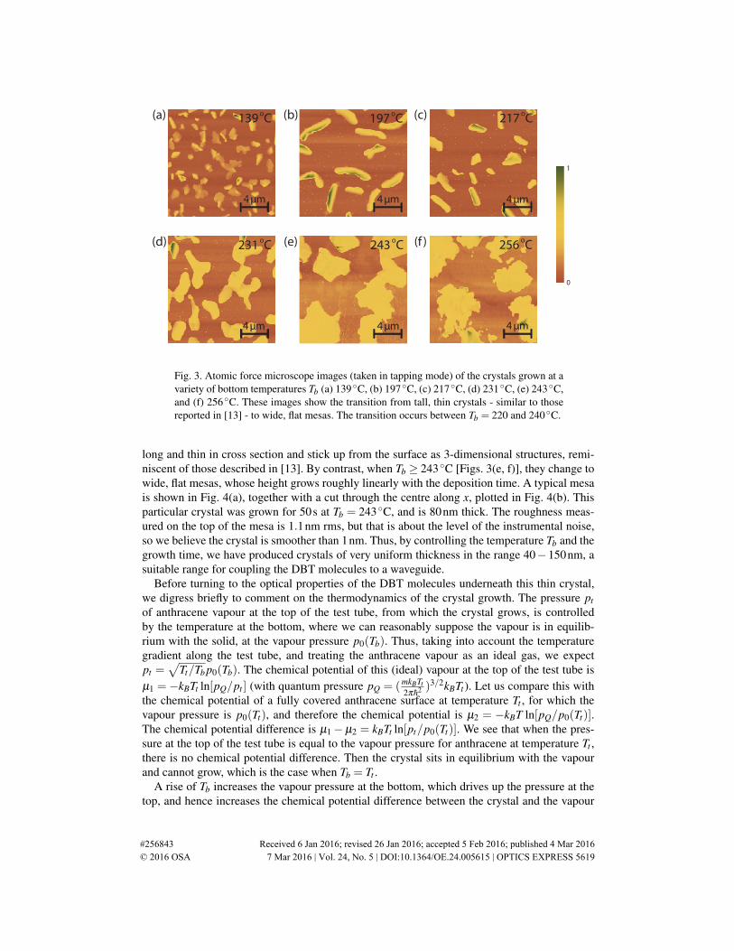
Changing Tb has a profound effect on the morphology of the crystals that grow, as we demon-strate in Fig. 3 – a set of atomic force microscope images showing crystals grown at succes-sively higher values of the bottom temperature. With Tb ≤ 218 C [Figs. 3(a-c)], the crystals are
#256843 Received 6 Jan 2016; revised 26 Jan 2016; accepted 5 Feb 2016; published 4 Mar 2016 © 2016 OSA 7 Mar 2016 | Vol. 24, No. 5 | DOI:10.1364/OE.24.005615 | OPTICS EXPRESS 5618
(a) (b) (c)
(d) (e) (f )
4 mμ 4 mμ 4 mμ
4 mμ 4 mμ 4 mμ
1
0
139 Co 217 Co
243 Co
197 Co
231 Co 256 Co
Fig. 3. Atomic force microscope images (taken in tapping mode) of the crystals grown at avariety of bottom temperatures Tb (a) 139C, (b) 197C, (c) 217C, (d) 231C, (e) 243C,and (f) 256C. These images show the transition from tall, thin crystals - similar to thosereported in [13] - to wide, flat mesas. The transition occurs between Tb = 220 and 240C.
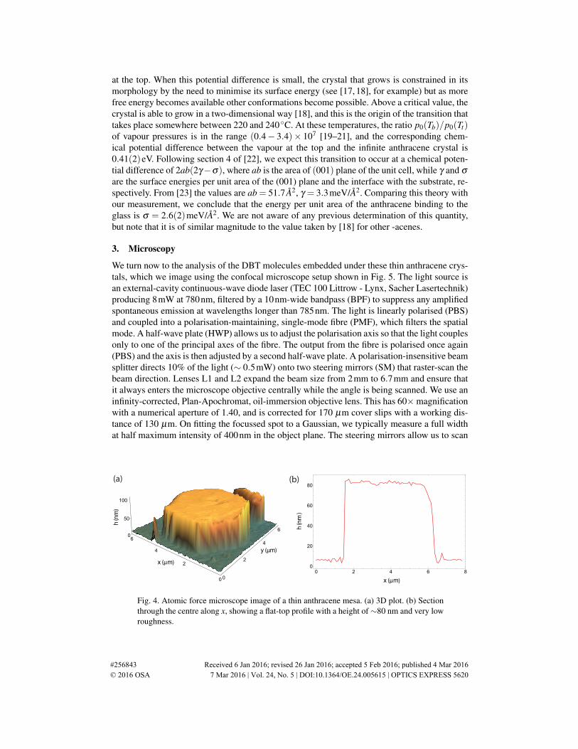
long and thin in cross section and stick up from the surface as 3-dimensional structures, remi-niscent of those described in [13]. By contrast, when Tb ≥ 243 C [Figs. 3(e, f)], they change towide, flat mesas, whose height grows roughly linearly with the deposition time. A typical mesais shown in Fig. 4(a), together with a cut through the centre along x, plotted in Fig. 4(b). Thisparticular crystal was grown for 50s at Tb = 243 C, and is 80nm thick. The roughness meas-ured on the top of the mesa is 1.1nm rms, but that is about the level of the instrumental noise,so we believe the crystal is smoother than 1nm. Thus, by controlling the temperature Tb and thegrowth time, we have produced crystals of very uniform thickness in the range 40−150nm, asuitable range for coupling the DBT molecules to a waveguide.
Before turning to the optical properties of the DBT molecules underneath this thin crystal,we digress briefly to comment on the thermodynamics of the crystal growth. The pressure ptof anthracene vapour at the top of the test tube, from which the crystal grows, is controlledby the temperature at the bottom, where we can reasonably suppose the vapour is in equilib-rium with the solid, at the vapour pressure p0(Tb). Thus, taking into account the temperaturegradient along the test tube, and treating the anthracene vapour as an ideal gas, we expectpt =
√Tt/Tb p0(Tb). The chemical potential of this (ideal) vapour at the top of the test tube is
µ1 = −kBTt ln[pQ/pt ] (with quantum pressure pQ = (mkBTt2π h2 )
3/2kBTt ). Let us compare this withthe chemical potential of a fully covered anthracene surface at temperature Tt , for which thevapour pressure is p0(Tt), and therefore the chemical potential is µ2 = −kBT ln[pQ/p0(Tt)].The chemical potential difference is µ1− µ2 = kBTt ln[pt/p0(Tt)]. We see that when the pres-sure at the top of the test tube is equal to the vapour pressure for anthracene at temperature Tt ,there is no chemical potential difference. Then the crystal sits in equilibrium with the vapourand cannot grow, which is the case when Tb = Tt .
A rise of Tb increases the vapour pressure at the bottom, which drives up the pressure at thetop, and hence increases the chemical potential difference between the crystal and the vapour
#256843 Received 6 Jan 2016; revised 26 Jan 2016; accepted 5 Feb 2016; published 4 Mar 2016 © 2016 OSA 7 Mar 2016 | Vol. 24, No. 5 | DOI:10.1364/OE.24.005615 | OPTICS EXPRESS 5619
at the top. When this potential difference is small, the crystal that grows is constrained in itsmorphology by the need to minimise its surface energy (see [17, 18], for example) but as morefree energy becomes available other conformations become possible. Above a critical value, thecrystal is able to grow in a two-dimensional way [18], and this is the origin of the transition thattakes place somewhere between 220 and 240C. At these temperatures, the ratio p0(Tb)/p0(Tt)of vapour pressures is in the range (0.4− 3.4)× 107 [19–21], and the corresponding chem-ical potential difference between the vapour at the top and the infinite anthracene crystal is0.41(2)eV. Following section 4 of [22], we expect this transition to occur at a chemical poten-tial difference of 2ab(2γ−σ), where ab is the area of (001) plane of the unit cell, while γ and σ
are the surface energies per unit area of the (001) plane and the interface with the substrate, re-spectively. From [23] the values are ab = 51.7 A2, γ = 3.3meV/A2. Comparing this theory withour measurement, we conclude that the energy per unit area of the anthracene binding to theglass is σ = 2.6(2)meV/A2. We are not aware of any previous determination of this quantity,but note that it is of similar magnitude to the value taken by [18] for other -acenes.
3. Microscopy
We turn now to the analysis of the DBT molecules embedded under these thin anthracene crys-tals, which we image using the confocal microscope setup shown in Fig. 5. The light source isan external-cavity continuous-wave diode laser (TEC 100 Littrow - Lynx, Sacher Lasertechnik)producing 8mW at 780nm, filtered by a 10nm-wide bandpass (BPF) to suppress any amplifiedspontaneous emission at wavelengths longer than 785nm. The light is linearly polarised (PBS)and coupled into a polarisation-maintaining, single-mode fibre (PMF), which filters the spatialmode. A half-wave plate (HWP) allows us to adjust the polarisation axis so that the light couplesonly to one of the principal axes of the fibre. The output from the fibre is polarised once again(PBS) and the axis is then adjusted by a second half-wave plate. A polarisation-insensitive beamsplitter directs 10% of the light (∼ 0.5mW) onto two steering mirrors (SM) that raster-scan thebeam direction. Lenses L1 and L2 expand the beam size from 2mm to 6.7mm and ensure thatit always enters the microscope objective centrally while the angle is being scanned. We use aninfinity-corrected, Plan-Apochromat, oil-immersion objective lens. This has 60×magnificationwith a numerical aperture of 1.40, and is corrected for 170 µm cover slips with a working dis-tance of 130 µm. On fitting the focussed spot to a Gaussian, we typically measure a full widthat half maximum intensity of 400nm in the object plane. The steering mirrors allow us to scan
0 2 4 6 80
20
40
60
80(a) (b)
x (μm)
y (μm)
0 0
2
4
6
2
4
60
50
100
h(n
m)
h(n
m)
x μm)(
Fig. 4. Atomic force microscope image of a thin anthracene mesa. (a) 3D plot. (b) Sectionthrough the centre along x, showing a flat-top profile with a height of∼80 nm and very lowroughness.
#256843 Received 6 Jan 2016; revised 26 Jan 2016; accepted 5 Feb 2016; published 4 Mar 2016 © 2016 OSA 7 Mar 2016 | Vol. 24, No. 5 | DOI:10.1364/OE.24.005615 | OPTICS EXPRESS 5620

this spot over an area of 20×20 µm.The 780nm laser excites molecules from the ground state S0 to the first excited singlet S1.
Although the laser frequency lies 2THz above the S0,0−S1,0 “zero-phonon” resonance of DBT,the homogeneous linewidth at room temperature is approximately 10THz, so molecules areexcited both to the S1,v=0 state at the bottom of the upper band and to vibrationally excited statesS1,v of the upper electronic level. These relax very rapidly to S1,0, which then decays radiativelyback to the ground level S0. The “zero-phonon” light is emitted at a wavelength of ∼ 785nm,while the transitions to vibrationally excited ground states S0,v produce sidebands further to thered. This fluorescence is collected by the microscope and retraces the path of the incident lightback as far as the beam splitter, where 90% of the photons are transmitted. A 792nm long-passfilter (LPF) rejects scattered excitation light – and also rejects DBT fluorescence close to thezero-phonon line – but transmits the more red-shifted sidebands of the fluorescence. This lightis coupled into a multimode fibre (MMF) and a fibre beam splitter delivers half the power toeach of two silicon avalanche photodiode detectors (Si-APD).
With the long-pass filter removed, there is a strong signal in the detectors from back-scattered780nm excitation light. Figure 6(a) shows six anthracene crystals, viewed in this way afterattenuating the excitation power to ∼ 1nW. The image in Fig. 6(b), taken with the long-pass
OBJECTIVE
3D Stage
X‐Y SM
L1
FCFC
90:10 BS
L2
HWP
Sample
Oil
PMF
MMFSi APD
Si APD50:50
Multimode Fiber BS
HWPFC PBS780 BPF
792 LPFPBS
780 nm CW Laser Source
Objective
Fig. 5. Schematic of our confocal microscope system. 780-BPF: 780 nm band pass filter;PBS: polarising beam splitter; HWP: half wave plate; FC: fiber coupler; PMF: polarisationmaintaining fiber; 90:10 BS: 90% transmission, 10% reflection cube beam splitter; X-YSM: X-Y steering mirrors; L1, L2: telecentric lens system f1 = 75mm, f2 = 250mm; Ob-jective: Nikon OFN25 DIC N2 60× microscope objective; 3D Stage: Thorlabs NanomaxMAX311/M translation stage for positioning the sample ; 792-LPF: Chroma technologyRET792LP long pass filter; MMF: multimode fiber; 50:50 Multimode Fiber BS: 50%transmission, 50% reflection multimode fiber beam splitter; Si APD: Perkin Elmer SPCM-AQRH-15-FC silicon avalanche photodiode detectors.
#256843 Received 6 Jan 2016; revised 26 Jan 2016; accepted 5 Feb 2016; published 4 Mar 2016 © 2016 OSA 7 Mar 2016 | Vol. 24, No. 5 | DOI:10.1364/OE.24.005615 | OPTICS EXPRESS 5621

filter in place and with the attenuator removed, shows the individual DBT molecules embeddedin the same crystals. These scans cover an area of 16×16 µm and have a resolution of 200×200pixels.
In order to have good control over the density of photo-emitters, we first deposit the DBTmolecules on the glass surface then over-coat them with anthracene, as described in section 2.We therefore needed to establish whether the molecules remain stuck on the surface, underneaththe crystal, or are incorporated into the anthracene matrix. DBT molecules occupying the mainsite in anthracene have the long axis of the terrylene moiety - and hence the S0− S1 opticaldipole moment - polarised along the b-axis of the crystal [11], whereas they must have a randomorientation when we first deposit them on the glass. Thus, our first test was to measure thefluorescence as a function of the polarisation angle of the excitation light, to see whether theDBT molecules in a given crystal share a common orientation. Figure 7(a) sums the two imagesin Fig. 6, to show the DBT molecules and the anthracene crystals simultaneously, and indicatesthree crystals, labeled (i - iii), where we have measured the DBT polarisation in some detail.In each crystal we identify molecules that are well isolated from each other, and for thosemolecules we measure the fluorescence intensity, normalised to incident power, as a functionof the polarisation angle θ . We determine the background level by measuring the signal from anearby place on the same crystal where there are no DBT molecules, and this is subtracted. Thepolar plots in Fig. 7(b) show the angular dependences measured in crystals (i - iii). In crystal (i)four out of the five molecules exhibit the same orientation, though one of these has quite poorcontrast. In crystal (ii) all six molecules have the same orientation, as do the three measured incrystal (iii). The lines drawn in Fig. 7(b) are fits of the form Acos2(θ +φ)+B/(A+B), with φ
being the direction of the molecular alignment. In all, we looked at 58 molecules in 12 crystalsand found, as summarised in Fig. 7(c), that the DBT molecules in a given crystal are indeedclosely aligned with each other. This provides strong evidence that the molecules move insidethe anthracene as it grows and become aligned with the b-axis of the crystal. It is possiblethat some of the dispersion in orientation is associated with DBT molecules that occupy thesecondary insertion site, known as the red site, where the orientation is rotated by 7 [11], butwe have not yet explored that possibility.
4. Optical properties of the DBT
In order to prove that the DBT fluorescence seen in Fig. 6(b) comes from individual molecules,we measure the correlation between photon arrival times in the two photodetectors [Fig. (5)]
(a) (b)
4 μm4 μm
Fig. 6. Confocal microscope images. (a) Anthracene crystals viewed in reflected excitationlight (long-pass filter removed). (b) The same crystals viewed with the long-pass filter inplace. Nearly all the spots are single DBT molecules.
#256843 Received 6 Jan 2016; revised 26 Jan 2016; accepted 5 Feb 2016; published 4 Mar 2016 © 2016 OSA 7 Mar 2016 | Vol. 24, No. 5 | DOI:10.1364/OE.24.005615 | OPTICS EXPRESS 5622

using a time-correlated counting card (TCCC, Picoquant Timeharp200) and a 755 nm, 83 pspulsed laser (Picoquant, PDL-800B). This determines the average probability of detecting aphoton in the second detector during a narrow time window δ t centred on time t + τ , havingpreviously registered one in the first detector at time t. For small enough δ t this is the discreteapproximation to the (unnormalised) second-order correlation function C(2)(τ) [24]
C(2)(τ) = 〈a†(t)a†(t + τ)a(t)a(t + τ)〉, (1)
where a† and a are the photon creation and annihilation operators, respectively. With δ t =106.9ps and an excitation power of 16 µW we have count rates of order 4× 10⁴ s−1 in eachdetector. Because the pulse repetition time ∆t = 25ns is substantially longer than the decaytime T1 of the excited state, we expect the correlation we measure to be well described by thefunction
C(2)(τ)' B+N∞
∑n=−∞
(1− δ0n
m)e−
|τ−n∆t|T1 , (2)
where B is a background due to dark counts in the detector, N is a normalising factor, n is aninteger that labels the excitation pulses, δ0n is the Kronecker delta, and m is the number ofmolecules emitting the light.
The black line plotted in Fig. 8 shows the experimental result obtained after 30 minutes ofmeasurement, while the red line is the fit of Eq. (2) to this measurement. We see that the centralpeak is strongly suppressed because we are observing a single molecule that is unable to emit
90 °
180 ° 0 °
270 °
90 °
180 ° 0 °
270 °
90 °
180 ° 0 °
270 °
- 40 - 20 0 20 400
2
4
6
8
10
Orientation relative to the mean ( )
No
.ofm
olec
ules
o
0
1
(a)
(b)
(c)
Visi
bilit
y(i) (ii) (iii)
(i)
(ii)
(iii)- 40 - 20 0 20 40
0
2
4
6
8
10
Orientation relative to crystal axis ( )
No.
ofm
olec
ules
o
Fig. 7. Test of DBT polarisation. (a) Sum of the two images from Fig. 6. (b) Normalisedpolar plots of molecule emission as the excitation laser polarisation angle is varied. Labels(i-iii) indicate the crystal in which the molecules reside, as shown in (a). The colour ofthe lines signifies the visibility of the fitted function to the data. Within a given crystalthe optical dipoles clearly share a common orientation. (c) Histogram showing the spreadof molecule orientations relative to the mean orientation, taken over 58 molecules in 12crystals.
#256843 Received 6 Jan 2016; revised 26 Jan 2016; accepted 5 Feb 2016; published 4 Mar 2016 © 2016 OSA 7 Mar 2016 | Vol. 24, No. 5 | DOI:10.1364/OE.24.005615 | OPTICS EXPRESS 5623

-60 -40 -20 0 20 40 600
200
400
600
800
t (ns)
C(2) (t)
Fig. 8. Second order correlation function of the light from a single fluorescent spot withina thin anthracene crystal when pumped with a pulsed laser. The reduced peak in the centreshows that this is a single DBT molecule. Black line: data accumulated over 30 minuteswith the timing resolution set to 106.9ps. Red line: fit to Eq.(2). Blue dashed line: back-ground level deduced from the fitted function.
two photons at once. The fit gives the number of molecules as m = 1.53(15), or in terms of thenormalised second-order correlation function, g(2)(0) = 1−1/m = 0.346(59). We interpret thisto mean that we are observing a single molecule, but that we also collect a small amount of lightfrom other nearby molecule(s) in the periphery of the field of view. By repeating this experimenton many different fluorescent spots we have established that virtually all the emitters are singlemolecules when the DBT density is low, as in Fig. 6. At higher density, we also see brightspots with higher central C(2) peaks, corresponding to clusters of two or more DBT molecules.Returning to Fig. 8, the blue dashed line shows the background level B = 44.7(2). The same fitgives the excited state lifetime as T1 = 4.23(5)ns, and this is typical of the lifetimes for all theemitters. It is also similar to the lifetimes measured in thick crystals [5–7,13] and in spin-coatedthin films [14].
When this same molecule is driven continuously by a laser on resonance, the scattering ratein steady state is given by the optical Bloch equations [25] as
R =I
I + IsatRmax , (3)
where I is the laser intensity at the molecule, Isat is the saturation intensity, and Rmax is thelimiting rate at high intensity. The saturation intensity is linked to the Rabi frequency Ω andto the relaxation times by I/Isat = Ω2T1T2. We have determined the saturation intensity of thismolecule by measuring the scattered photon rate as a function of the incident intensity, as shownby the points plotted in Fig. 9. The red line is a fit of Eq. (3) to the data, which gives the resultIsat = 75(3)kW/cm2. We are not aware of any other determination of this parameter, but notethat closely related data are also presented in [14].
When dye molecules are optically excited it is not unusual for them to react with ambi-ent oxygen molecules and stop fluorescing [26], which is clearly undesirable in a practicalsingle-photon source. In order to see whether oxygen plays an important role here, we grewDBT-doped crystals in an atmosphere of air instead of purging the glove bag with nitrogen.We then illuminated 36 molecules, one at a time, at a wavelength of 780nm and an inten-sity of ∼ 10kW/cm2 (s ' 0.13) and recorded how long each molecule survived before photo-
#256843 Received 6 Jan 2016; revised 26 Jan 2016; accepted 5 Feb 2016; published 4 Mar 2016 © 2016 OSA 7 Mar 2016 | Vol. 24, No. 5 | DOI:10.1364/OE.24.005615 | OPTICS EXPRESS 5624

bleaching. The orange squares in Fig. 10 show the number of molecules remaining unbleachedas a function of the illumination time. This evolution is reasonably well described by an ex-ponential decay, with a lifetime of 5.7s, as shown by the solid line. That corresponds to amolecule being excited (on average) ∼ 107 times before it photo-bleaches. Nicolet et al. [5]give the branching ratio for decay from S1 to the triplet state T0 as ∼ 10−7, so our result couldindicate that the photobleaching mechanism here is associated with passing through the tripletstate of DBT and subsequent reaction with the oxygen. However, DBT molecules on the sur-face of the slide, without any anthracene on top, bleach so quickly that they do not have time topass through the triplet state – indeed so quickly that we could not make a plot of their survivalover time – so, at least in that case, the triplet state of DBT does not seem to be playing a rolein the bleaching.
By contrast, the DBT molecules prepared without oxygen are extremely photostable. In orderto measure their bleaching, we removed LI and used L2 – shown in Fig. 5 – to focus theexcitation light onto the back aperture of the objective. This illuminated a circle of 9.3 µmFWHM in the plane of the sample, allowing us to expose all the molecules in a single crystal.We also used much higher laser power (125 mW from a Toptica TA 100 Pro at 780nm) sothat the intensity on each molecule increased to ∼ 130 kW/cm2 (s' 1.7). We then interleavedperiods of high-intensity exposure with confocal scans to check how many molecules remainedunbleached. The result, plotted using blue circles in Fig. 10, shows that these molecules areremarkably stable. An initial population of 75 molecules, observed in 3 separate crystals, decaysto 60 molecules after a minute, to 32 after an hour, and to 30 after 4 hours and 20 minutes. Thisevolution cannot be described by an exponential: the loss rate per molecule is much higher atearly times than it is at later times. To illustrate this, the solid blue line in Fig. 10 shows thatthis data can be described by the simple empirical formula 15e(−t/5.7) + 31e(−t/103) + 30. Atthe end of this experiment, the 30 photostable molecules have survived > 1012 excitations, andit seems likely that they could have survived many more. It remains to be seen whether all themolecules can be rendered photostable by a more serious effort to remove all the oxygen.
0 50 100 150 200 250 3000
100
200
300
400
Intensity (kW/cm2)
DetectedPhotons
(kC/s)
Fig. 9. A typical plot of detected molecule emission for various illumination intensities,showing a saturation intensity of Isat = 75(3) kW/cm2 and a maximum count rate of Rmax =440 kC/s. Red line: fit to the data using Eq. 3.
#256843 Received 6 Jan 2016; revised 26 Jan 2016; accepted 5 Feb 2016; published 4 Mar 2016 © 2016 OSA 7 Mar 2016 | Vol. 24, No. 5 | DOI:10.1364/OE.24.005615 | OPTICS EXPRESS 5625

5. Conclusions
We have demonstrated a method for growing anthracene crystals that are wide and thin. Thethickness, adjustable by the duration of the growth over the range 40− 150nm (at least),has excellent uniformity. A highly supersaturated anthracene vapour is used to obtain enoughchemical potential difference to favour this morphology. The anthracene is doped with DBTmolecules that are spun onto the surface prior to the crystal growth, and this makes it possi-ble to adjust the concentration of the dopant over a wide range. We have shown that after theanthracene is grown, the DBT molecules become aligned with a common axis in the crystal– presumably the b-axis – which indicates that they are accepted into the lattice, where mostof them occupy the main insertion site. This opens the possibility of aligning the moleculeswith nano-fabricated optical structures when we seek in the future to insert them into devices.The standard Hanbury Brown and Twiss method has shown that the bright spots seen in themicroscope are indeed single molecules, and the decay of the exponentials in the C(2) functionhave shown that the lifetime in these particular crystals is similar to that in other anthracenematrices. We have also measured the saturation intensity at room temperature and find that it isunremarkable. On subjecting these molecules to a long period of intense illumination, we findthat they are extremely photostable as long as we grow the anthracene in a nitrogen atmosphere,rather than in air. We presume that this hinges on the level of oxygen.
In summary, there is a need for quantum emitters able to radiate individual photons ondemand into optical nanostructures, and we have started to pursue the proposal that DBTmolecules in an organic matrix might be able to satisfy that need. Having shown that the matrixmust be thin to achieve efficient coupling to a waveguide, we have found a way to grow suitablefilms of anthracene, and how to dope them with DBT. On investigating their optical properties,we find that these molecules are very promising, being both polarised and photostable. This
1 10 100 1000 104
0
20
40
60
80
t (s)
No.ofmolecules
Fig. 10. Photo-bleaching of DBT in thin anthracene crystals. The graphs show the num-ber of DBT molecules remaining unbleached as a function of the exposure time. Orangesquares: Anthracene grown in an atmosphere of air and excited at 780 nm using an intensityof 10kW/cm2. Orange line: a fit to exponential decay, giving a lifetime of 5.7s. Blue Cir-cles: Anthracene grown in a nitrogen atmosphere and excited at 780 nm with 130kW/cm2.Blue line: simple empirical formula 15e(−t/5.7)+31e(−t/103)+30 intended to show that thedecay rate per molecule increases with time and hence that the bleaching is not exponential.
#256843 Received 6 Jan 2016; revised 26 Jan 2016; accepted 5 Feb 2016; published 4 Mar 2016 © 2016 OSA 7 Mar 2016 | Vol. 24, No. 5 | DOI:10.1364/OE.24.005615 | OPTICS EXPRESS 5626

stable emission at room temperature is immediately useful for quantum communication andsome quantum sensors. For applications that require interference between different photons,such as linear optical quantum computing, one needs to generate identical photons. That re-quires cooling to cryogenic temperatures, an investigation that is now under way. Whilst allof the anthracene growth presented in this paper was carried out on a glass substrate we haverecently grown crystals on silicon nitride, a material commonly used for nanophotonic devicesoperating at visible wavelengths. We find that these crystals appear to be the same as thosepresented here.
Acknowledgments
We are indebted to Jaesuk Hwang for suggesting this method of crystal growth, to Kiang-WeiKho for helping to set up the microscope, to Yu Hung Lien for valuable discussions, and to JonDyne, Steve Maine, and Valerijus Gerulis for their expert mechanical and electrical workshopsupport. We acknowledge funding from the Royal Society, the EPSRC, and dstl. The Euro-pean Commission supports A.S.C. through a Marie Skłodowska Curie Individual Fellowship(Q-MoPS) and S.G. through the Action-Initial Training Network: Frontiers in Quantum Tech-nology.
#256843 Received 6 Jan 2016; revised 26 Jan 2016; accepted 5 Feb 2016; published 4 Mar 2016 © 2016 OSA 7 Mar 2016 | Vol. 24, No. 5 | DOI:10.1364/OE.24.005615 | OPTICS EXPRESS 5627