Stability Analysis and Measurement of RC and RL Digital...
4
Stability Analysis and Measurement of RC and RL Digital Non-Foster Circuits with Latency Patrick J. Kehoe, Killian K. Steer, and Thomas P. Weldon Department of Electrical and Computer Engineering University of North Carolina at Charlotte Charlotte, NC, USA [email protected] Abstract—Stability analysis and measurements are presented for negative capacitance and negative inductance designs of digital non-Foster circuits that include a series resistance and model the effects of latency. Such digital non-Foster circuits provide a new important alternative to analog non-Foster circuits, with potential to address stability and performance issues in important non-Foster application areas such as metamaterials, acoustic cloaking, and electrically-small antennas. The proposed approach includes a resistive component in the signal processing of digital non-Foster RC and RL circuits to help control stability and to mitigate parasitic resistance, and also includes latency ef- fects associated with computation and conversion time. Analysis, simulation, and measured results confirm the desired non-Foster impedances, and show useful regions of stability as a function of resistance and latency. I. I NTRODUCTION Non-Foster circuits such as negative capacitors and negative inductors are of importance in enabling a number of exotic emerging technologies such as acoustic invisibility [1], [2], su- perluminal waveguides [3], [4], software-designed radios and electrically-small antennas beyond the Wheeler-Chu limit [5]– [8], and metamaterials [9], [10]. Notwithstanding so many promising applications, stability remains a central design issue with non-Foster circuits [11], [12]. More recently, digital non-Foster circuits have been proposed, with the potential of leveraging inherent advantages of digital technology to design repeatably stable digital implementations of non-Foster circuits [13], [14]. The following extends prior stability results in [15] to new Th´ evenin-form digital non-Foster RC (resistor-capacitor) and RL (resistor-inductor) circuits in [16] that have a voltage- output DAC (digital-to-analog converter), and that include the effects of latency associated with computation time and DAC and ADC (analog-to-digital converter) conversion times. Prior digital non-Foster stability analyses were limited to Norton- form implementations with a current-output DAC, and did not include effects of series resistance and latency [15]. The new stability analysis also considers a series resistance that is included within the signal processing of the digital non- Foster circuit, to provide additional control of stability, and to mitigate parasitic resistance. Therefore, root locus analyses for these new digital non-Foster configurations are presented below, to determine stable regions of operation. In the following section, background theory is reviewed for Th´ evenin-form digital discrete-time non-Foster RC and RL circuits. In Section III, stability theory is presented and root locus analysis is used to determine stable regions of operation. Lastly, measured results are provided for several stable prototype circuits and compared against theoretical results. II. DIGITAL NON-FOSTER RC AND RL THEORY Before proceeding with root locus stability analysis in the following section, the theory of Th´ evenin-form digital discrete-time non-Foster circuits is reviewed [16]. In Fig. 1, a Th´ evenin-form digital non-Foster circuit is driven by an ex- ternal Norton current source. Non-Foster input voltage v in (t) is converted into discrete time signal v in [n]= v in (nT ) by the ADC with clock period T . Signal processing block H(z) pro- duces the voltage-output DAC signal v dac [n]= h[n] ⇤ v in [n]. The final DAC output v dac (t) typically includes a ZOH (zero- order hold) and latency effects (associated with computa- tion time and DAC and ADC conversion times) modeled as time delay ⌧ . Also, the DAC has a finite source resistance (and/or added external resistance), which is represented by R dac . From R dac , the input current is i in (t)=[v in (t) - v dac (t)]/R dac . The Laplace transform, assuming a ZOH, gives V dac (s)= V ? in (s)H(z)(1 - z -1 )e -s⌧ /s z=e sT where Fig. 1. Block diagram of a Th´ evenin-form digital discrete-time non-Foster circuit [13] driven by external Norton current source is(t) [15]. ADC with clock period T converts input voltage into v in [n]= v in (nT ), with filter H(z) output v dac [n]= h[n] ⇤ v in [n], DAC output voltage v dac (t), latency ⌧ , and current i in (t)=[v in (t) - v dac (t)]/R dac . 978–1–5386–1539–3/17/$31.00 c 2017 IEEE
Transcript of Stability Analysis and Measurement of RC and RL Digital...

Stability Analysis and Measurement of RC and RLDigital Non-Foster Circuits with Latency
Patrick J. Kehoe, Killian K. Steer, and Thomas P. WeldonDepartment of Electrical and Computer Engineering
University of North Carolina at CharlotteCharlotte, NC, [email protected]
Abstract—Stability analysis and measurements are presented
for negative capacitance and negative inductance designs of
digital non-Foster circuits that include a series resistance and
model the effects of latency. Such digital non-Foster circuits
provide a new important alternative to analog non-Foster circuits,
with potential to address stability and performance issues in
important non-Foster application areas such as metamaterials,
acoustic cloaking, and electrically-small antennas. The proposed
approach includes a resistive component in the signal processing
of digital non-Foster RC and RL circuits to help control stability
and to mitigate parasitic resistance, and also includes latency ef-
fects associated with computation and conversion time. Analysis,
simulation, and measured results confirm the desired non-Foster
impedances, and show useful regions of stability as a function of
resistance and latency.
I. INTRODUCTION
Non-Foster circuits such as negative capacitors and negativeinductors are of importance in enabling a number of exoticemerging technologies such as acoustic invisibility [1], [2], su-perluminal waveguides [3], [4], software-designed radios andelectrically-small antennas beyond the Wheeler-Chu limit [5]–[8], and metamaterials [9], [10]. Notwithstanding so manypromising applications, stability remains a central design issuewith non-Foster circuits [11], [12]. More recently, digitalnon-Foster circuits have been proposed, with the potentialof leveraging inherent advantages of digital technology todesign repeatably stable digital implementations of non-Fostercircuits [13], [14].
The following extends prior stability results in [15] to newThevenin-form digital non-Foster RC (resistor-capacitor) andRL (resistor-inductor) circuits in [16] that have a voltage-output DAC (digital-to-analog converter), and that include theeffects of latency associated with computation time and DACand ADC (analog-to-digital converter) conversion times. Priordigital non-Foster stability analyses were limited to Norton-form implementations with a current-output DAC, and didnot include effects of series resistance and latency [15]. Thenew stability analysis also considers a series resistance thatis included within the signal processing of the digital non-Foster circuit, to provide additional control of stability, andto mitigate parasitic resistance. Therefore, root locus analysesfor these new digital non-Foster configurations are presentedbelow, to determine stable regions of operation.
In the following section, background theory is reviewedfor Thevenin-form digital discrete-time non-Foster RC andRL circuits. In Section III, stability theory is presented androot locus analysis is used to determine stable regions ofoperation. Lastly, measured results are provided for severalstable prototype circuits and compared against theoreticalresults.
II. DIGITAL NON-FOSTER RC AND RL THEORY
Before proceeding with root locus stability analysis inthe following section, the theory of Thevenin-form digitaldiscrete-time non-Foster circuits is reviewed [16]. In Fig. 1, aThevenin-form digital non-Foster circuit is driven by an ex-ternal Norton current source. Non-Foster input voltage vin(t)is converted into discrete time signal vin[n] = vin(nT ) by theADC with clock period T . Signal processing block H(z) pro-duces the voltage-output DAC signal vdac[n] = h[n] ⇤ vin[n].The final DAC output vdac(t) typically includes a ZOH (zero-order hold) and latency effects (associated with computa-tion time and DAC and ADC conversion times) modeled astime delay ⌧ . Also, the DAC has a finite source resistance(and/or added external resistance), which is represented byRdac. From Rdac, the input current is iin(t) = [vin(t) �vdac(t)]/Rdac. The Laplace transform, assuming a ZOH,gives Vdac(s) = V ?
in(s)H(z)(1� z�1)e�s⌧/s��z=esT
where
Fig. 1. Block diagram of a Thevenin-form digital discrete-time non-Fostercircuit [13] driven by external Norton current source is(t) [15]. ADC withclock period T converts input voltage into vin[n] = vin(nT ), with filterH(z) output vdac[n] = h[n] ⇤ vin[n], DAC output voltage vdac(t), latency⌧ , and current iin(t) = [vin(t)� vdac(t)]/Rdac.
978–1–5386–1539–3/17/$31.00 c� 2017 IEEE
Copyright 2017 IEEE. Published in 2017 IEEE SoutheastCon, Charlotte, NC, 31 Mar - 2 Apr, 2017. Personal use of this material is permitted. However, permission to reprint/republish this material for advertising or promotional purposes or for creating new collective works for resale or redistribution to servers or lists, or to reuse any copyrighted component of this work in other works, must be obtained from the IEEE, 445 Hoes Lane, Piscataway, NJ 08855, USA. Tel.: 908-562-3966. See http://ieeexplore.ieee.org/search/searchresult.jsp?newsearch=true&queryText=Stability%20Analysis%20and%20Measurement%20of%20RC%20and%20RL%20Digital%20Non-Foster%20Circuits%20with%20Latency .

Fig. 2. Root locus stability analysis of G(z) for a digital non-Foster RC circuitelement with C = �8 nF, and Rser varied from �85 ohms to 115 ohms insteps of 20. The edge of stability occurs near Rser ⇡ 100 ohms. Otherparameters were Rs = 50 ohms, Rdac = 1000 ohms, � = 1, and T =1120 ns. Poles are denoted ”X,” and zeroes denoted ”O.”
V ?(s) =P
v(nT )e�nsT is the the starred transform [17]. Forvin(t) sampled at 0.5/T Hz without aliasing, the impedanceof the digital non-Foster circuit element in the dashed box onthe right side of Fig. 1 is [16]
Zin(s) =Vin(s)
Iin(s)⇡ sT Rdac
sT �H(z)(1� z�1)e�s⌧
����z=esT
. (1)
The circuit of Fig. 1 and (1) can be used to design a range ofdigital implementations of non-Foster circuits, such as negativecapacitors, negative inductors, and the non-Foster RC and RLcircuits in [16].
For present purposes, first consider an analog series RCcircuit with capacitance C and resistance Rser. For thiscircuit, v(t) = i(t)Rser +
Ri(t)dt/C. Next, taking the
derivative gives dvin(t)/dt = Rserdiin(t)/dt + iin(t)/C.Approximating, dvin(t)/dt ⇡ (vin[n]� vin[n� 1])/T andiin[n] ⇡ (vin[n] � vdac[n])/Rdac, the circuit can be realizedas vdac[n] (RserC + T ) = vin[n] (RserC �RdacC + T ) +vin[n� 1] (RdacC �RserC) + vdac[n� 1]RserC. Taking thez-transform yields H(z) for the digital series RC [16]
HRC(z) =(RserC �RdacC + T ) z + (RdacC �RserC)
(RserC + T ) z �RserC. (2)
The same approach can be applied to an analog se-ries RL circuit with inductance L and resistance Rser. Forthis circuit, v(t) = Ldi(t)/dt + i(t)Rser. Approximatingdiin(t)/dt ⇡ (iin[n]� iin[n� 1])/T and with iin[n] ⇡(vin[n] � vdac[n])/Rdac , the equation can be realized asvdac[n] (1 +RserT/L) � vdac[n � 1] = vin[n](1 + RserT/L�RdacT/L)�vin[n�1]. Taking the z-transform yields [16]
HRL(z) =(L+RserT �RdacT ) z � L
(L+RserT ) z � L(3)
III. STABILITY ANALYSIS
When the non-Foster RC element is connected to the Nortonsource, as seen in Fig. 1, the closed-loop system transfer func-tion relating the source current to the non-Foster input current
Fig. 3. Root locus stability analysis of G(z) for a digital non-Foster RLcircuit element with L = �0.5 mH, and Rser varied from �500 ohms to0 ohms in steps of 100. The edge of stability occurs near Rser ⇡ �50 ohms.Other parameters were Rs = 50 ohms, Rdac = 1000 ohms, � = 1, andT = 1260 ns. Poles are denoted ”X,” and zeroes denoted ”O.”
(DAC current) is G(s) = Iin(s)/Is(s) with correspondingdiscrete-time transfer function [15], [17]
G(z) =�Rez
��H(z)/Rdac
1�Rez��H(z)/Rdac, (4)
where � is the (integer) latency in clock cycles, Re =RsRdac/(Rs+Rdac) is the parallel combination of the sourceand DAC resistances, and Vin(z)H(z)z��/Rdac would be theNorton-equivalent current of the Thevenin source comprised ofthe voltage-output DAC in series with Rdac. Then, the systemof Fig. 1 is stable as long as the poles of G(z) in (4) lie withinthe unit circle [17].
Root locus analysis was performed on (4) to investigatethe range of stable values of Rser. The example of Fig. 2shows the root locus plot for a digital non-Foster RC designof a C = �8 nF capacitor, as Rser was increased from�85 ohms to 115 ohms in steps of 20. Other parametersfor H(z) = HRC(z) in Fig. 2 were T = 1120 ns, Rdac =1000 ohms, � = 1, and Rs = 50 ohms. At Rser = �85 ohms,the two poles of G(z) are well within the unit circle. Thepoles become unstable and move outside the unit circle atRser = 115 in Fig. 2. The stability boundary was observednear Rser ⇡ 100 ohms, with instability for Rser > 100 ohms.
Similarly, the root locus plot of Fig. 3 is for a digital non-Foster RL design of a L = �0.5 mH inductor, as Rser wasincreased from �500 ohms to 0 ohms in steps of 100. Otherparameters for H(z) = HRL(z) in Fig. 3 were T = 1260 ns,Rdac = 1000 ohms, � = 1, and Rs = 50 ohms. At Rser =�500 ohms, the two poles of G(z) are well within the unitcircle, and move outside the unit circle at Rser = 0. Thestability boundary was observed near Rser ⇡ �50 ohms, withinstability for Rser > �50 ohms.
An additional root locus shown in Fig. 4 was performedon the series RC circuit to determine the effect of latency onsystem stability. Again, other parameters for H(z) = HRC(z)were T = 1120 ns, C = �8 nF, Rdac = 1000 ohms, Rser =

Fig. 4. Root locus stability analysis of G(z) for a digital non-Foster RCcircuit element with C = -8 nF, Rs = 50 ohms, Rser = 0 ohms, Rdac =1000 ohms, T = 1120 ns, and latency � is varied from 0 to 5 clock cyclesin steps of 1. Poles are denoted ”X,” and zeroes denoted ”O.”
0 ohms, and Rs = 50 ohms. Latency was increased from � =0 to � = 5 clock cycles in integer steps, and the system poleswere found to be inside the unit circle and stable for all cases.Note also, that the number of poles increases with the latencyat each step. Somewhat surprisingly, as latency increased to amaximum of 5 clock cycles, the system remained stable forthis particular example.
IV. PROTOTYPE AND MEASUREMENTS
The NXP FRDM-K64F board shown in Fig. 5 was usedto build prototypes of digital RC and RL non-Foster circuits,since this microcontroller has an on-board 16-bit ADC and 12-bit DAC. The transfer functions for the RC and RL systemsas given in (2) and (3) respectively, were programmed ontothe FRDM-K64F micro-controller.
First, a series RC digital discrete-time non-Foster circuitwas built and measured. The system was designed to havecapacitance C = �8 nF, and measurements were taken fortwo values of Rser within the stable region of the root locusof Fig. 2, with Rser = 0 ohms and Rser = 50 ohms. Themeasured results for Zin are given in Fig. 6 for Rser =0 ohms, and in Fig. 7 for Rser = 50 ohms. In both figures,the solid red and dotted blue lines represent the real andimaginary parts of the theoretical input impedance Zin, andthe magenta short-dashed and cyan long-dashed lines arethe real and imaginary components of the measured inputimpedance. In Fig. 6, at 0.05 MHz, the measured input
Fig. 5. Prototype digital non-Foster circuit using an NXP FRDM-K64Fdevelopment board to implement the system of Fig. 1.
Fig. 6. Measured and theoretical input impedance Zin for a digital seriesRC circuit of Fig. 1, where Rser = 0 ohms, T = 1120 ns, C = �8 nF,Rdac = 1000 ohms, and the latency ⌧ = 1120 ns. Solid red and dotted blueare real and imaginary parts of theoretical Zin, and the magenta short-dashedand cyan long-dashed line are real and imaginary parts of measured Zin.
impedance was �302 + j273 ohms, and the theoretical inputimpedance at 0.05 MHz was calculated as �357+j341 ohms.In Fig. 7, at 0.05 MHz, the measured input impedance was�234+ j294 ohms, and the theoretical input impedance from(1) at 0.05 MHz was calculated as �299+j390 ohms. Ideally,C = �8 nF would be j398 ohms at 0.05 MHz. In Fig. 6and Fig. 7, a period of 1120 ns was used, corresponding to asampling frequency of approximately 893 kHz, an externalDAC resistance of Rdac = 1000 ohms was added, andprocessing time plus ADC and DAC conversion times led toan observed latency of approx. 1 clock cycle. In both figures,the shape of the reactance curve, Im(Zin), at low frequencyhas the expected form, exhibiting the predicted change in signdue to the negative capacitance value.
Next, a series RL digital discrete-time non-Foster circuitwas built and measured. The system was designed to haveinductance L = �0.5 mH, and measurements were taken fortwo values of Rser within the stable region of the root locusof Fig. 3, with Rser = �50 ohms and Rser = �100 ohms.The measured results for Zin are given in Fig. 8 for Rser =�50 ohms, and in Fig. 9 for Rser = �100 ohms. In both fig-
Fig. 7. Measured and theoretical input impedance Zin for a digital seriesRC circuit of Fig. 1, where Rser = 50 ohms, T = 1120 ns, C = �8 nF,Rdac = 1000 ohms, and the latency ⌧ = 1120 ns. Solid red and dotted blueare real and imaginary parts of theoretical Zin, and the magenta short-dashedand cyan long-dashed line are real and imaginary parts of measured Zin.
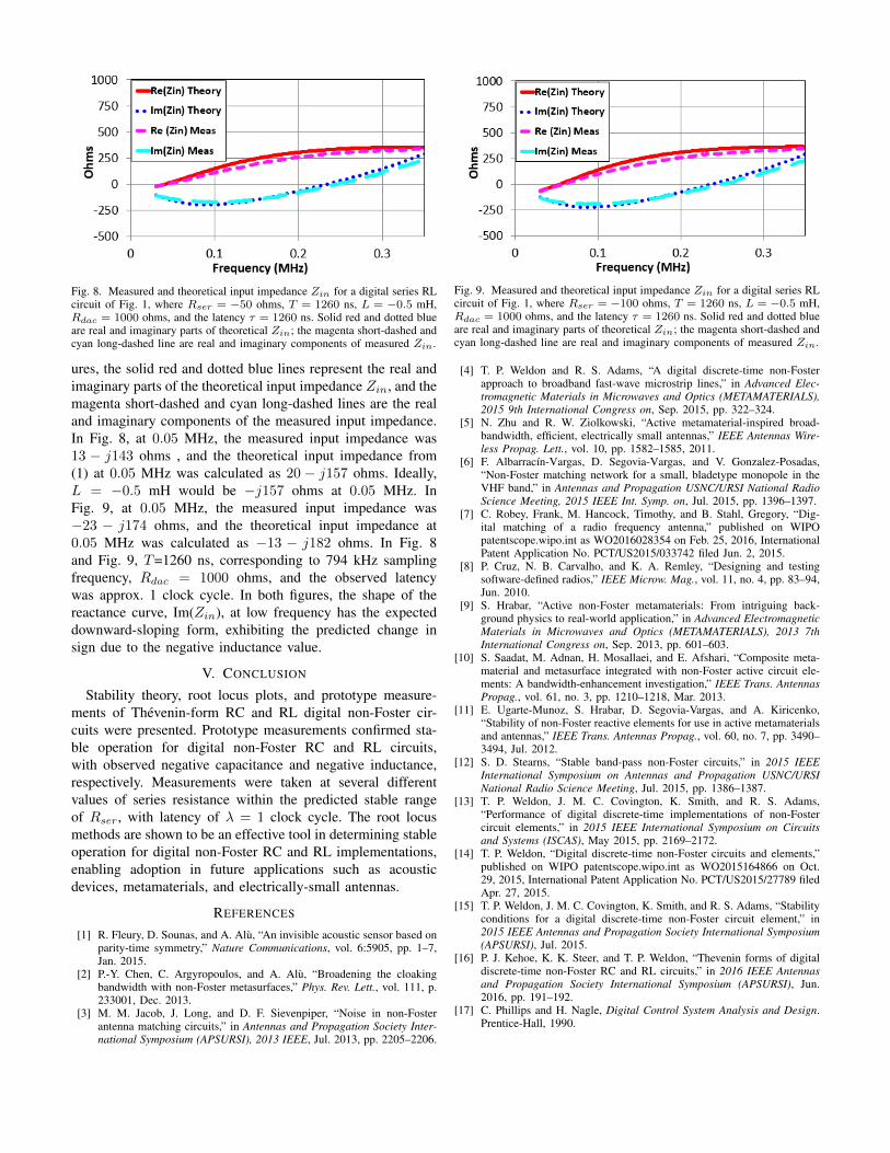
Fig. 8. Measured and theoretical input impedance Zin for a digital series RLcircuit of Fig. 1, where Rser = �50 ohms, T = 1260 ns, L = �0.5 mH,Rdac = 1000 ohms, and the latency ⌧ = 1260 ns. Solid red and dotted blueare real and imaginary parts of theoretical Zin; the magenta short-dashed andcyan long-dashed line are real and imaginary components of measured Zin.
ures, the solid red and dotted blue lines represent the real andimaginary parts of the theoretical input impedance Zin, and themagenta short-dashed and cyan long-dashed lines are the realand imaginary components of the measured input impedance.In Fig. 8, at 0.05 MHz, the measured input impedance was13 � j143 ohms , and the theoretical input impedance from(1) at 0.05 MHz was calculated as 20 � j157 ohms. Ideally,L = �0.5 mH would be �j157 ohms at 0.05 MHz. InFig. 9, at 0.05 MHz, the measured input impedance was�23 � j174 ohms, and the theoretical input impedance at0.05 MHz was calculated as �13 � j182 ohms. In Fig. 8and Fig. 9, T=1260 ns, corresponding to 794 kHz samplingfrequency, Rdac = 1000 ohms, and the observed latencywas approx. 1 clock cycle. In both figures, the shape of thereactance curve, Im(Zin), at low frequency has the expecteddownward-sloping form, exhibiting the predicted change insign due to the negative inductance value.
V. CONCLUSION
Stability theory, root locus plots, and prototype measure-ments of Thevenin-form RC and RL digital non-Foster cir-cuits were presented. Prototype measurements confirmed sta-ble operation for digital non-Foster RC and RL circuits,with observed negative capacitance and negative inductance,respectively. Measurements were taken at several differentvalues of series resistance within the predicted stable rangeof Rser, with latency of � = 1 clock cycle. The root locusmethods are shown to be an effective tool in determining stableoperation for digital non-Foster RC and RL implementations,enabling adoption in future applications such as acousticdevices, metamaterials, and electrically-small antennas.
REFERENCES
[1] R. Fleury, D. Sounas, and A. Alu, “An invisible acoustic sensor based onparity-time symmetry,” Nature Communications, vol. 6:5905, pp. 1–7,Jan. 2015.
[2] P.-Y. Chen, C. Argyropoulos, and A. Alu, “Broadening the cloakingbandwidth with non-Foster metasurfaces,” Phys. Rev. Lett., vol. 111, p.233001, Dec. 2013.
[3] M. M. Jacob, J. Long, and D. F. Sievenpiper, “Noise in non-Fosterantenna matching circuits,” in Antennas and Propagation Society Inter-national Symposium (APSURSI), 2013 IEEE, Jul. 2013, pp. 2205–2206.
Fig. 9. Measured and theoretical input impedance Zin for a digital series RLcircuit of Fig. 1, where Rser = �100 ohms, T = 1260 ns, L = �0.5 mH,Rdac = 1000 ohms, and the latency ⌧ = 1260 ns. Solid red and dotted blueare real and imaginary parts of theoretical Zin; the magenta short-dashed andcyan long-dashed line are real and imaginary components of measured Zin.
[4] T. P. Weldon and R. S. Adams, “A digital discrete-time non-Fosterapproach to broadband fast-wave microstrip lines,” in Advanced Elec-tromagnetic Materials in Microwaves and Optics (METAMATERIALS),2015 9th International Congress on, Sep. 2015, pp. 322–324.
[5] N. Zhu and R. W. Ziolkowski, “Active metamaterial-inspired broad-bandwidth, efficient, electrically small antennas,” IEEE Antennas Wire-less Propag. Lett., vol. 10, pp. 1582–1585, 2011.
[6] F. Albarracın-Vargas, D. Segovia-Vargas, and V. Gonzalez-Posadas,“Non-Foster matching network for a small, bladetype monopole in theVHF band,” in Antennas and Propagation USNC/URSI National RadioScience Meeting, 2015 IEEE Int. Symp. on, Jul. 2015, pp. 1396–1397.
[7] C. Robey, Frank, M. Hancock, Timothy, and B. Stahl, Gregory, “Dig-ital matching of a radio frequency antenna,” published on WIPOpatentscope.wipo.int as WO2016028354 on Feb. 25, 2016, InternationalPatent Application No. PCT/US2015/033742 filed Jun. 2, 2015.
[8] P. Cruz, N. B. Carvalho, and K. A. Remley, “Designing and testingsoftware-defined radios,” IEEE Microw. Mag., vol. 11, no. 4, pp. 83–94,Jun. 2010.
[9] S. Hrabar, “Active non-Foster metamaterials: From intriguing back-ground physics to real-world application,” in Advanced ElectromagneticMaterials in Microwaves and Optics (METAMATERIALS), 2013 7thInternational Congress on, Sep. 2013, pp. 601–603.
[10] S. Saadat, M. Adnan, H. Mosallaei, and E. Afshari, “Composite meta-material and metasurface integrated with non-Foster active circuit ele-ments: A bandwidth-enhancement investigation,” IEEE Trans. AntennasPropag., vol. 61, no. 3, pp. 1210–1218, Mar. 2013.
[11] E. Ugarte-Munoz, S. Hrabar, D. Segovia-Vargas, and A. Kiricenko,“Stability of non-Foster reactive elements for use in active metamaterialsand antennas,” IEEE Trans. Antennas Propag., vol. 60, no. 7, pp. 3490–3494, Jul. 2012.
[12] S. D. Stearns, “Stable band-pass non-Foster circuits,” in 2015 IEEEInternational Symposium on Antennas and Propagation USNC/URSINational Radio Science Meeting, Jul. 2015, pp. 1386–1387.
[13] T. P. Weldon, J. M. C. Covington, K. Smith, and R. S. Adams,“Performance of digital discrete-time implementations of non-Fostercircuit elements,” in 2015 IEEE International Symposium on Circuitsand Systems (ISCAS), May 2015, pp. 2169–2172.
[14] T. P. Weldon, “Digital discrete-time non-Foster circuits and elements,”published on WIPO patentscope.wipo.int as WO2015164866 on Oct.29, 2015, International Patent Application No. PCT/US2015/27789 filedApr. 27, 2015.
[15] T. P. Weldon, J. M. C. Covington, K. Smith, and R. S. Adams, “Stabilityconditions for a digital discrete-time non-Foster circuit element,” in2015 IEEE Antennas and Propagation Society International Symposium(APSURSI), Jul. 2015.
[16] P. J. Kehoe, K. K. Steer, and T. P. Weldon, “Thevenin forms of digitaldiscrete-time non-Foster RC and RL circuits,” in 2016 IEEE Antennasand Propagation Society International Symposium (APSURSI), Jun.2016, pp. 191–192.
[17] C. Phillips and H. Nagle, Digital Control System Analysis and Design.Prentice-Hall, 1990.