ST Strategy on 3D Integration LSI - semi.org 3D strategy Semi Janv... · ST Strategy on 3D...
22
ST Strategy on 3D Integration LSI Alexis Farcy, Nicolas Hotellier, Jean Michailos 3D Interconnects Front-End Manufacturing & Process R&D, Digital Sector STMicroelectronics 1 January 23, 2013 - Grenoble
Transcript of ST Strategy on 3D Integration LSI - semi.org 3D strategy Semi Janv... · ST Strategy on 3D...
ST Strategy on 3D Integration LSI
Alexis Farcy, Nicolas Hotellier, Jean Michailos
3D InterconnectsFront-End Manufacturing & Process R&D, Digital SectorSTMicroelectronics
1
January 23, 2013 - Grenoble
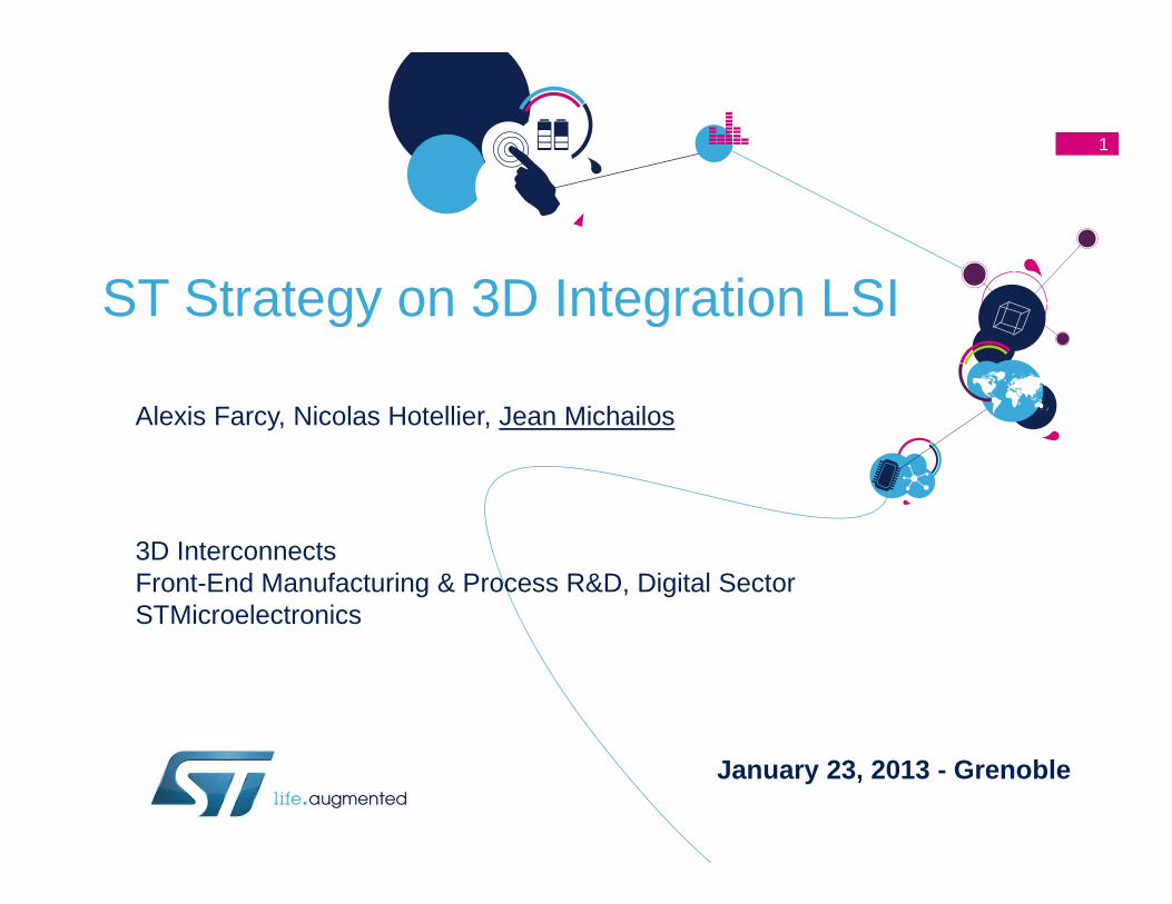
2Outline
• ST's competitiveness moving to 3D
• Via Middle Technology• Front side and Back side Process• Key process steps and challenges
• Electrical characterizations• Via Middle impact on electrical parameters & yield• Reliability assessment
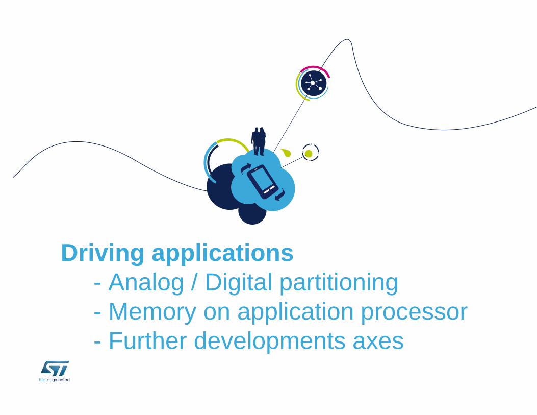
• Driving Applications• Analog / Digital partitioning• Memory on application processor• Further developments axes
• Conclusion & Perspectives
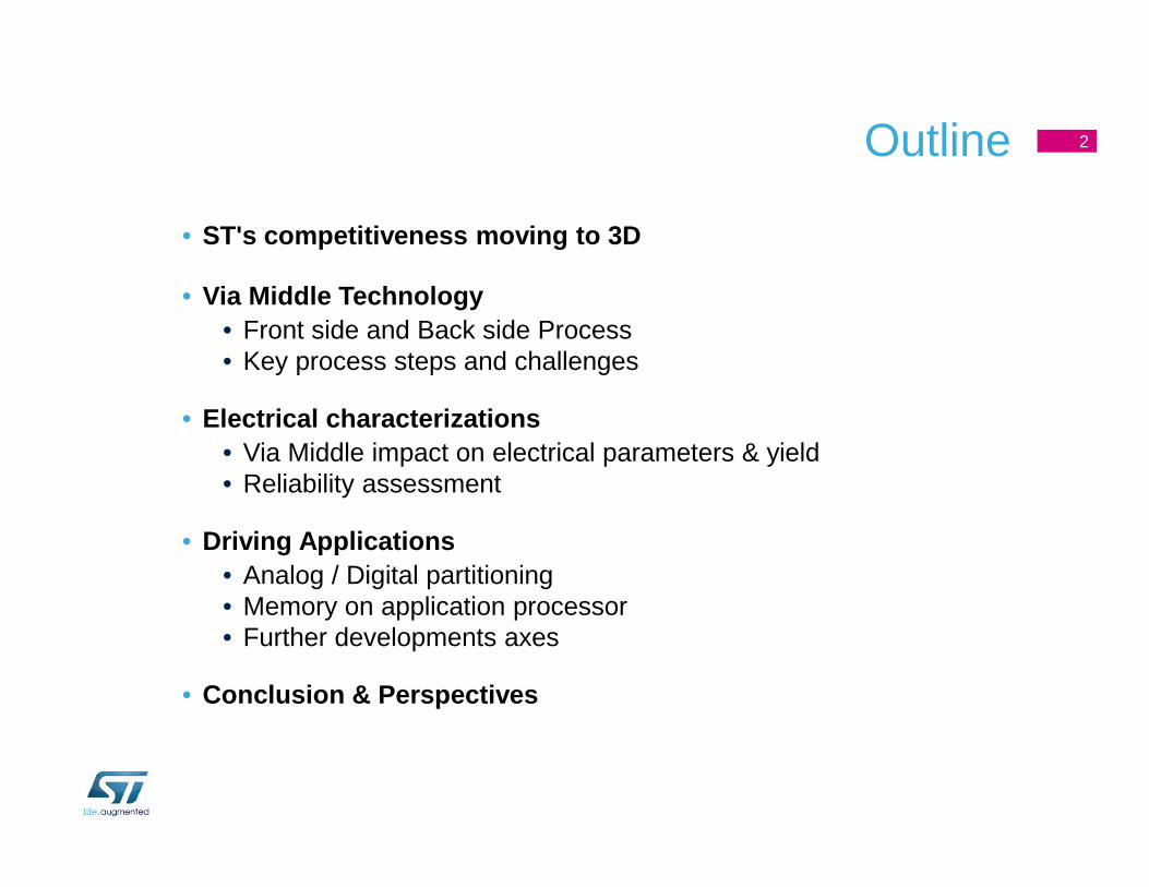
ST's competitiveness moving to 3D
• Our industry is looking for a complementary technology to the traditional 2D SoC or SiP design approach continuing to:
• Improve performances (enlarge bandwidth, enhance speed, reduce power consumption)
• Enlarge integration (reuse of existing IP, heterogeneous ICs, mixed technologies)
• Form Factor (Shrink feature sizes, Product partitioning )
• Lower cost (Reduce metal layer, Increase yield, Faster time to Market)
• 3D Interconnects provides another path with relatively smaller capital investments .
Source :Xilinx Source :IBM
3
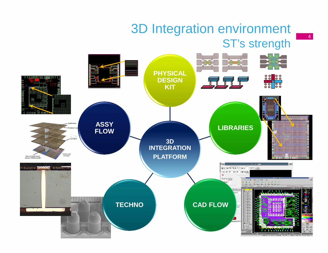
3D INTEGRATION
PLATFORM
PHYSICALDESIGN
KIT
LIBRARIES
CAD FLOWTECHNO
ASSY FLOW
43D Integration environment
ST’s strength
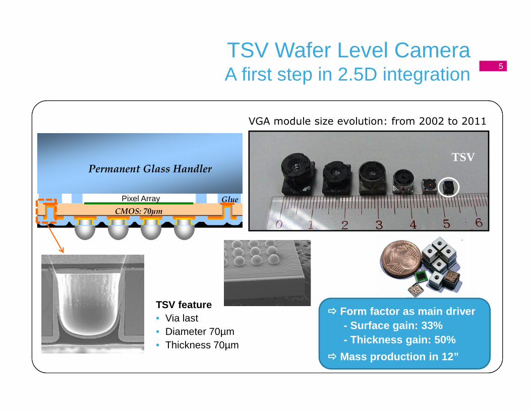
Pixel Array
Permanent Glass Handler
CMOS: 70µm
Glue
TSV
VGA module size evolution: from 2002 to 2011
5TSV Wafer Level Camera A first step in 2.5D integration
Form factor as main driver- Surface gain: 33%- Thickness gain: 50%
Mass production in 12”
TSV feature• Via last• Diameter 70µm• Thickness 70µm
Via Middle Technology- Front side and Back side Process- Key process steps and challenges
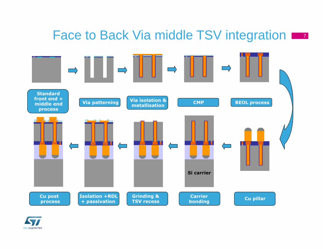
Standard front end + middle end process
Via patterningVia isolation & metallisation
CMP BEOL process
Cu pillarIsolation +RDL + passivation
Cu postprocess
Si carrier
Grinding & TSV recess
Carrier bonding
7Face to Back Via middle TSV integration
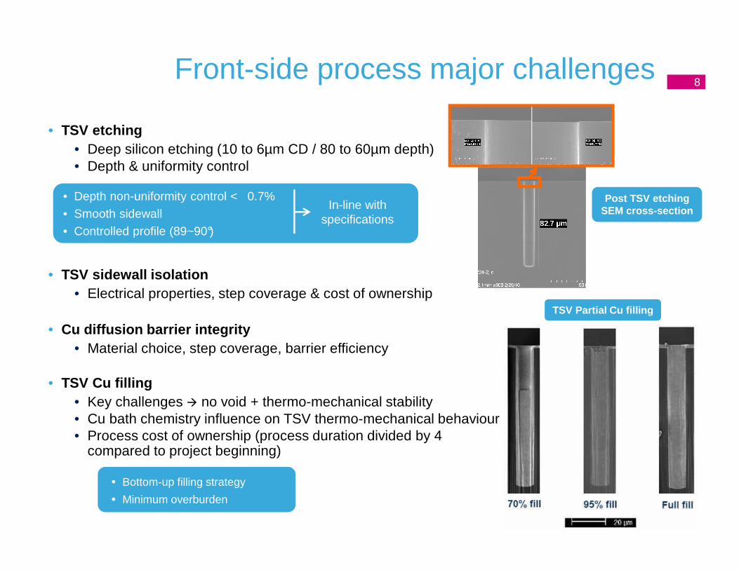
TSV Partial Cu filling
8Front-side process major challenges
• TSV sidewall isolation• Electrical properties, step coverage & cost of ownership
• TSV Cu filling• Key challenges no void + thermo-mechanical stability• Cu bath chemistry influence on TSV thermo-mechanical behaviour• Process cost of ownership (process duration divided by 4
compared to project beginning)
• Cu diffusion barrier integrity• Material choice, step coverage, barrier efficiency
• TSV etching• Deep silicon etching (10 to 6µm CD / 80 to 60µm depth)• Depth & uniformity control
• Depth non-uniformity control < 0.7%• Smooth sidewall• Controlled profile (89~90°)
In-line with specifications
• Bottom-up filling strategy
• Minimum overburden
Post TSV etching SEM cross-section
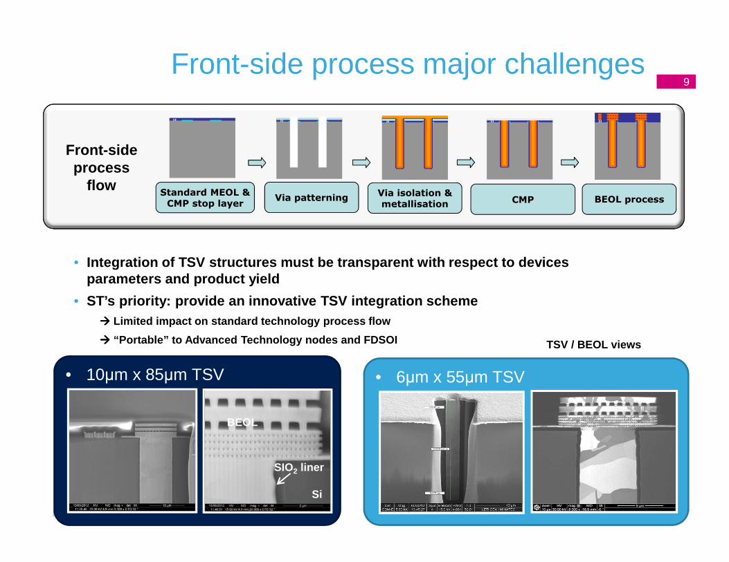
Front-side process
flow
Front-side process major challenges
• Integration of TSV structures must be transparent w ith respect to devices parameters and product yield
• ST’s priority: provide an innovative TSV integratio n scheme Limited impact on standard technology process flow
“Portable” to Advanced Technology nodes and FDSOI
BEOL processCMPVia isolation & metallisation
Via patterningStandard MEOL & CMP stop layer
9
TSV / BEOL views
BEOL• 10µm x 85µm TSV
Si
SIO2 liner
BEOL
• 6µm x 55µm TSV
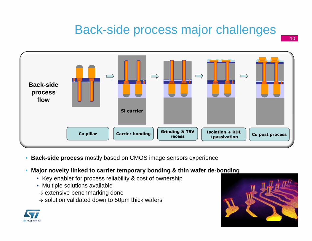
Back-side process
flow
Back-side process major challenges
Cu post processIsolation + RDL +passivation
Grinding & TSV recess
Carrier bondingCu pillar
10
Si carrier
• Back-side process mostly based on CMOS image sensors experience
• Major novelty linked to carrier temporary bonding & thin wafer de-bonding • Key enabler for process reliability & cost of ownership• Multiple solutions available extensive benchmarking done solution validated down to 50µm thick wafers
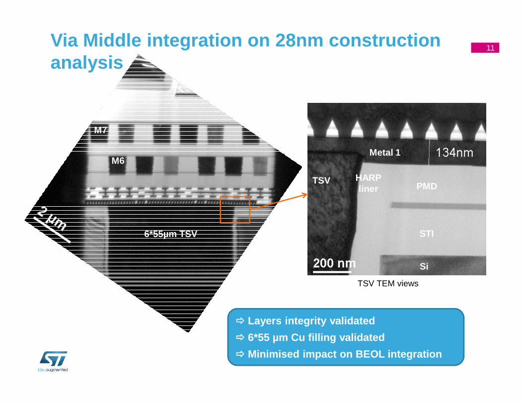
Via Middle integration on 28nm construction analysis
11
M6
Si
STI
Metal 1
TSVPMD
M7
HARPliner
6*55µm TSV
TSV TEM views
Layers integrity validated
6*55 µm Cu filling validated
Minimised impact on BEOL integration
Electrical characterizations- Via Middle impact on electrical parameters & yield- Reliability assessment
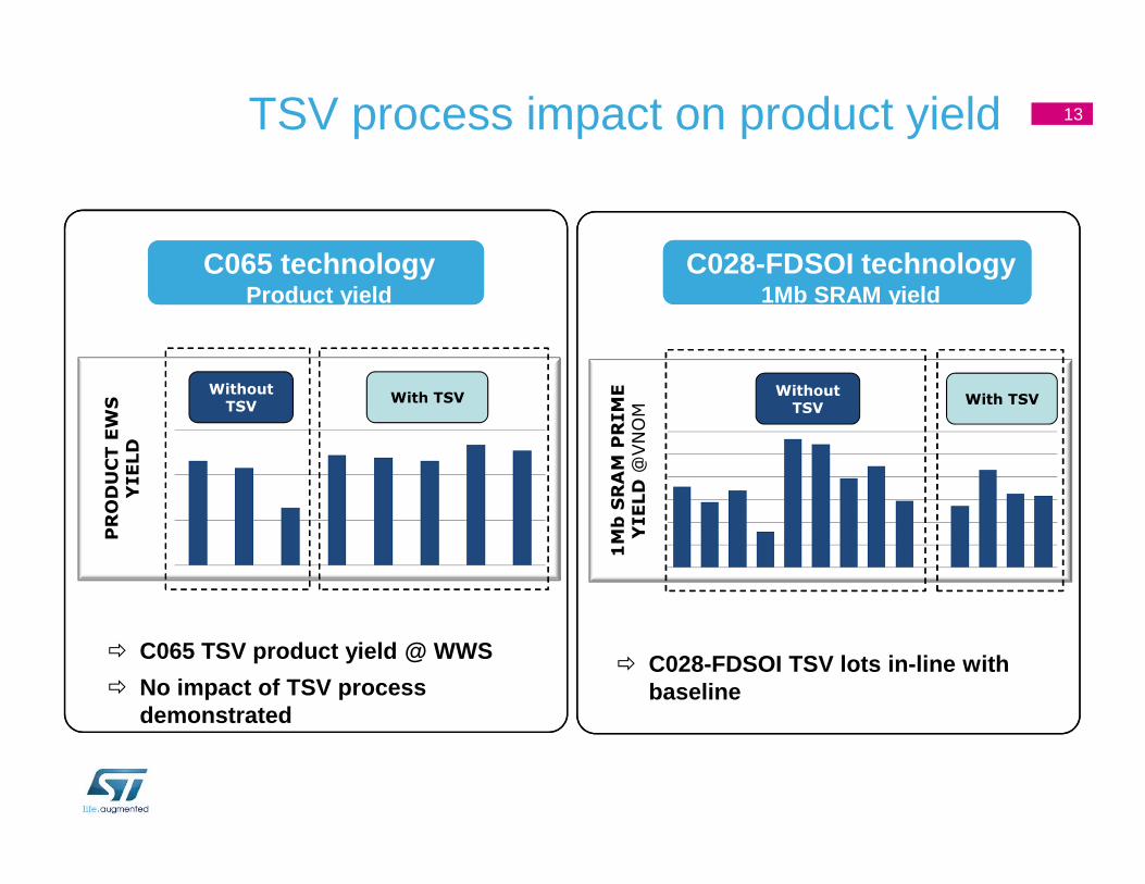
TSV process impact on product yield 13
C065 technologyProduct yield
C065 TSV product yield @ WWS
No impact of TSV process demonstrated
C028-FDSOI technology1Mb SRAM yield
PRODUCT EWS
YIELD
With TSVWithoutTSV
With TSVWithoutTSV
1Mb SRAM PRIME
YIELD @VNOM
C028-FDSOI TSV lots in-line with baseline
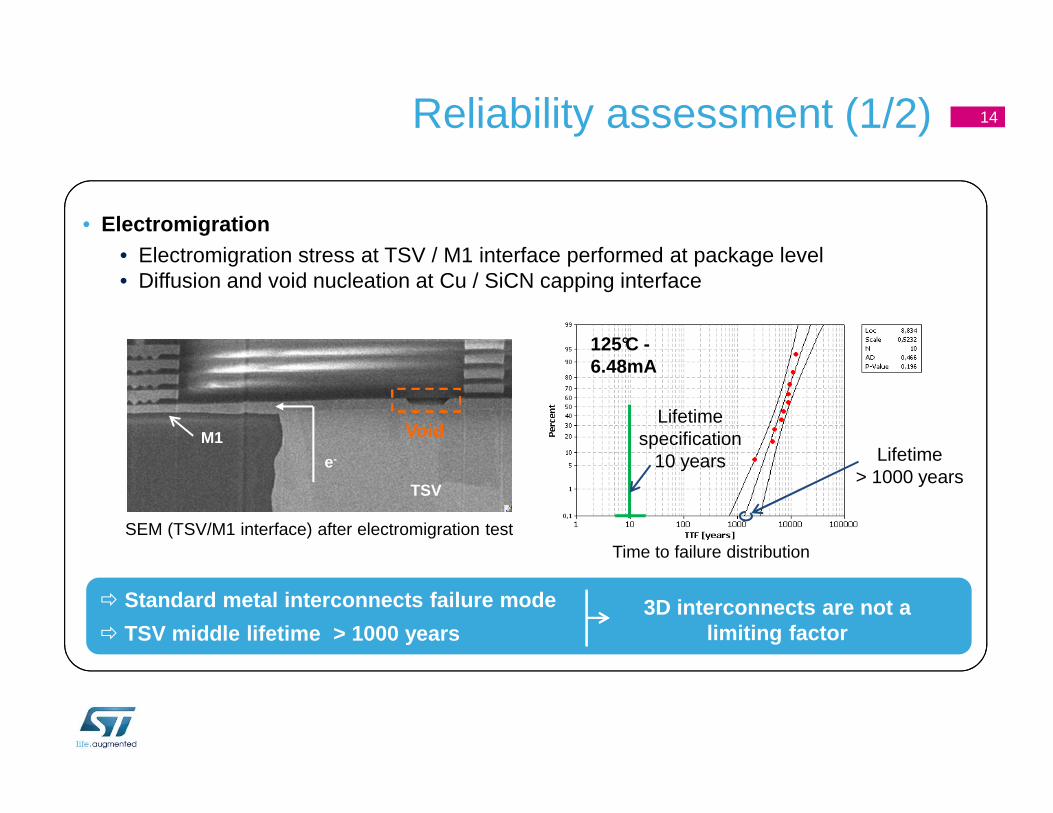
Reliability assessment (1/2) 14
Standard metal interconnects failure mode
TSV middle lifetime > 1000 years
• Electromigration• Electromigration stress at TSV / M1 interface performed at package level• Diffusion and void nucleation at Cu / SiCN capping interface
e-
M1 Void
TSV
SEM (TSV/M1 interface) after electromigration test
3D interconnects are not a limiting factor
Lifetime specification
10 years
125°C -6.48mA
Lifetime> 1000 years
Time to failure distribution
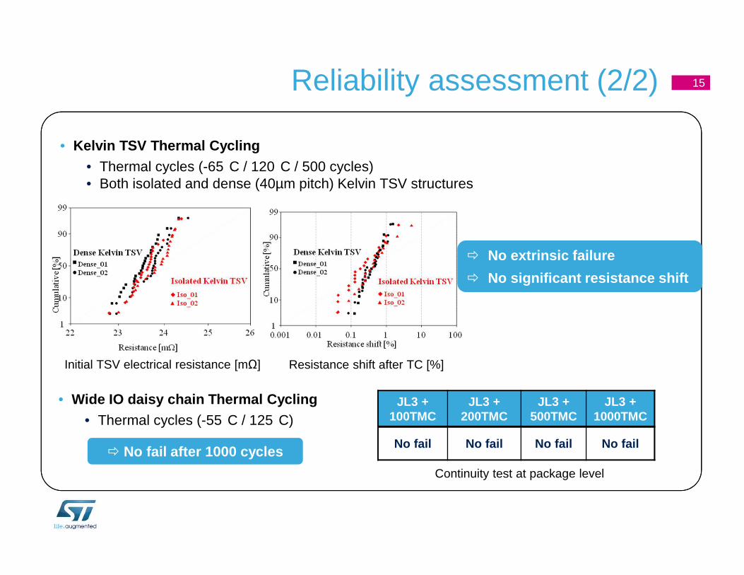
Reliability assessment (2/2) 15
No fail after 1000 cycles
• Kelvin TSV Thermal Cycling• Thermal cycles (-65 C / 120 C / 500 cycles)• Both isolated and dense (40µm pitch) Kelvin TSV structures
• Wide IO daisy chain Thermal Cycling• Thermal cycles (-55 C / 125 C)
JL3 +100TMC
JL3 +200TMC
JL3 +500TMC
JL3 +1000TMC
No fail No fail No fail No fail
Continuity test at package level
No extrinsic failure
No significant resistance shift
Initial TSV electrical resistance [mΩ] Resistance shift after TC [%]
Driving applications- Analog / Digital partitioning- Memory on application processor- Further developments axes
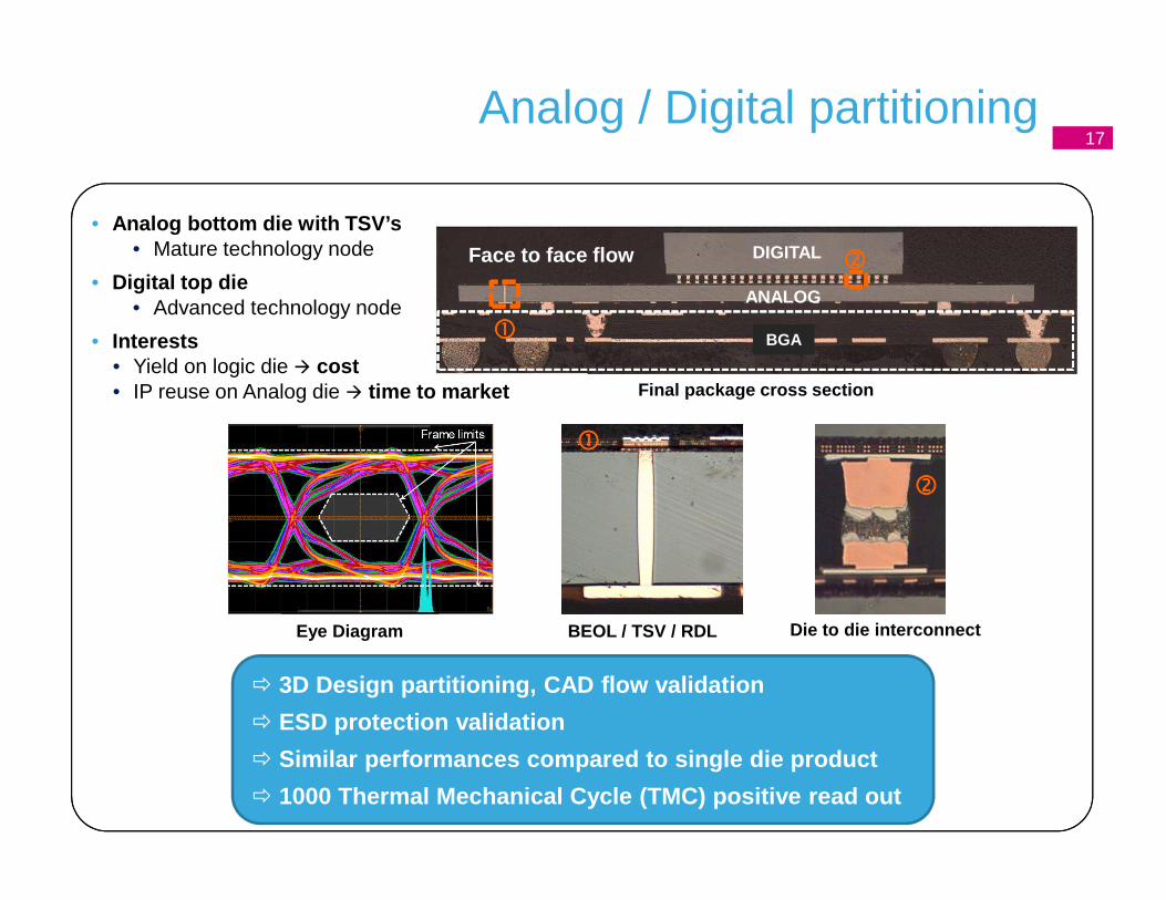
17Analog / Digital partitioning
3D Design partitioning, CAD flow validation
ESD protection validation
Similar performances compared to single die product
1000 Thermal Mechanical Cycle (TMC) positive read o ut
• Analog bottom die with TSV’s• Mature technology node
• Digital top die• Advanced technology node
• Interests• Yield on logic die cost• IP reuse on Analog die time to market
BGA
Face to face flow DIGITAL
ANALOG
Eye Diagram BEOL / TSV / RDL Die to die interconnect
Final package cross section

18
WIDE IO DRAM
SoCµ-pad
TSV
BGA
Cu pillar
WIDE IO DRAMSoC
Memory on Application processorBreakthrough in power efficiency
WIDE IO DRAM
• System on Chip co-designed by ST-E / ST / LETI • SoC key figures
• 73 mm2
• 1250 TSV’s & top / bottom interconnections• ~1000 flip chip Cu pillars (bottom / BGA)
Face to back flow
Full functionality demonstrated on first assembly lot
High final test yield
Performances in-line with JEDEC Wide IO specificati ons
SOC floor plan
TSV / µ-buffer array
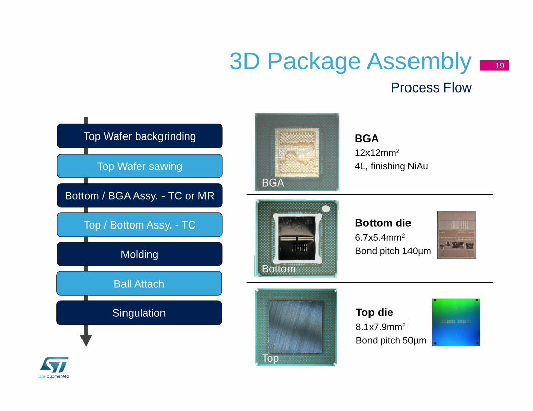
3D Package AssemblyProcess Flow
19
Top Wafer sawing
Top Wafer backgrinding
Top / Bottom Assy. - TC
Ball Attach
Singulation
Molding
Bottom / BGA Assy. - TC or MR
BGA12x12mm2
4L, finishing NiAu
Bottom die6.7x5.4mm2
Bond pitch 140µm
Top die8.1x7.9mm2
Bond pitch 50µm
BGA
Bottom
Top
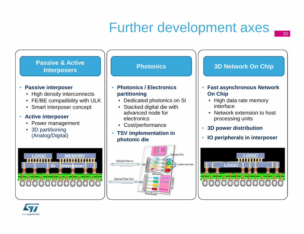
20Further development axes
Photonics 3D Network On Chip
• Photonics / Electronics partitioning• Dedicated photonics on Si• Stacked digital die with
advanced node for electronics
• Cost/performance
• TSV implementation in photonic die
• Fast asynchronous Network On Chip• High data rate memory
interface• Network extension to host
processing units
• 3D power distribution
• IO peripherals in interposer
Passive & Active Interposers
MEMORYLOGIC
Si Interposer
• Passive interposer• High density interconnects• FE/BE compatibility with ULK• Smart interposer concept
• Active interposer• Power management• 3D partitioning
(Analog/Digital)
LOGIC
LOGIC
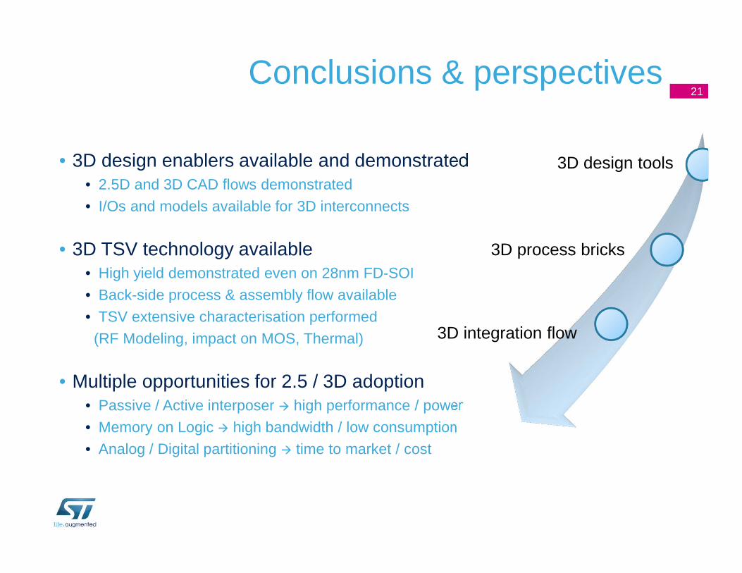
• 3D design enablers available and demonstrated• 2.5D and 3D CAD flows demonstrated
• I/Os and models available for 3D interconnects
• 3D TSV technology available• High yield demonstrated even on 28nm FD-SOI
• Back-side process & assembly flow available
• TSV extensive characterisation performed
(RF Modeling, impact on MOS, Thermal)
• Multiple opportunities for 2.5 / 3D adoption• Passive / Active interposer high performance / power
• Memory on Logic high bandwidth / low consumption
• Analog / Digital partitioning time to market / cost
21Conclusions & perspectives
3D process bricks
3D design tools
3D integration flow
• Many thanks to the whole teams within ST (Crolles and Grenoblesites), ST-Ericsson and CEA-LETI involved in the realization of theseworks
• Thank you for your attention
22Acknowledgements