SSD1306 - China LCD Module Manufacturer for … · ssd1306 rev 1.5 p 3/64 aug 2010 solomon systech...
64
SOLOMON SYSTECH SEMICONDUCTOR TECHNICAL DATA This document contains information on a new product. Specifications and information herein are subject to change without notice. http://www.solomon-systech.com SSD1306 Rev 1.5 P 1/64 Aug 2010 Copyright © 2010 Solomon Systech Limited Advance Information SSD1306 128 x 64 Dot Matrix OLED/PLED Segment/Common Driver with Controller
Transcript of SSD1306 - China LCD Module Manufacturer for … · ssd1306 rev 1.5 p 3/64 aug 2010 solomon systech...
SOLOMON SYSTECH SEMICONDUCTOR TECHNICAL DATA
This document contains information on a new product Specifications and information herein are subject to change without notice httpwwwsolomon-systechcom SSD1306 Rev 15 P 164 Aug 2010 Copyright copy 2010 Solomon Systech Limited
Advance Information
SSD1306
128 x 64 Dot Matrix OLEDPLED SegmentCommon Driver with Controller
Solomon Systech Aug 2010 P 264 Rev 15 SSD1306
Appendix IC Revision history of SSD1306 Specification
Version Change Items Effective Date
10 1st release
3-Oct-07
11 1 Revise typo 2 Revise command table
29-Apr-08
12 1 Add Charge pump section 2 Add Advance graphic commands 23h D6h
07-Jul-09
13 1 Revise Section 810 Charge Pump Regulator 2 Revise Section 12 DC Characteristics 3 Revise min tAS Address Setup Time in Table 13-2 to 5ns 4 Add Figure 10-7 Oscillator frequency setting 5 Update declaimer
07-May-10
14 1 Replace SSD1306Z by SSD1306Z2 and add SSD1306Z2 into ordering information (P7)
2 Add Power ON and OFF sequence with Charge Pump Application in section 89 (p29)
13-Jul-10
15 1 Update Power onoff sequence with charge pump application in section 89 (p29)
27-Aug-10
SSD1306 Rev 15 P 364 Aug 2010 Solomon Systech
CONTENTS
1 GENERAL DESCRIPTION 7
2 FEATURES7
3 ORDERING INFORMATION 7
4 BLOCK DIAGRAM 8
5 DIE PAD FLOOR PLAN 9
6 PIN ARRANGEMENT12 61 SSD1306TR1 PIN ASSIGNMENT 12
7 PIN DESCRIPTION 14
8 FUNCTIONAL BLOCK DESCRIPTIONS16 81 MCU INTERFACE SELECTION 16
811 MCU Parallel 6800-series Interface 16 812 MCU Parallel 8080-series Interface 17 813 MCU Serial Interface (4-wire SPI) 18 814 MCU Serial Interface (3-wire SPI) 19 815 MCU I2C Interface 20
82 COMMAND DECODER 23 83 OSCILLATOR CIRCUIT AND DISPLAY TIME GENERATOR 23 84 FR SYNCHRONIZATION 24 85 RESET CIRCUIT 24 86 SEGMENT DRIVERS COMMON DRIVERS 25 87 GRAPHIC DISPLAY DATA RAM (GDDRAM) 26 88 SEGCOM DRIVING BLOCK 27 89 POWER ON AND OFF SEQUENCE 28
891 Power ON and OFF sequence with External VCC 28 892 Power ON and OFF sequence with Charge Pump Application 29
810 CHARGE PUMP REGULATOR 30 9 COMMAND TABLE 30
91 DATA READ WRITE 36 10 COMMAND DESCRIPTIONS 37
101 FUNDAMENTAL COMMAND 37 1011 Set Lower Column Start Address for Page Addressing Mode (00h~0Fh) 37 1012 Set Higher Column Start Address for Page Addressing Mode (10h~1Fh) 37 1013 Set Memory Addressing Mode (20h) 37 1014 Set Column Address (21h) 38 1015 Set Page Address (22h) 39 1016 Set Display Start Line (40h~7Fh) 39 1017 Set Contrast Control for BANK0 (81h) 39 1018 Set Segment Re-map (A0hA1h) 39 1019 Entire Display ON (A4hA5h) 40 10110 Set NormalInverse Display (A6hA7h) 40 10111 Set Multiplex Ratio (A8h) 40 10112 Set Display ONOFF (AEhAFh) 40 10113 Set Page Start Address for Page Addressing Mode (B0h~B7h) 40 10114 Set COM Output Scan Direction (C0hC8h) 40 10115 Set Display Offset (D3h) 40 10116 Set Display Clock Divide Ratio Oscillator Frequency (D5h) 43
Solomon Systech Aug 2010 P 464 Rev 15 SSD1306
10117 Set Pre-charge Period (D9h) 43 10118 Set COM Pins Hardware Configuration (DAh) 44 10119 Set VCOMH Deselect Level (DBh) 46 10120 NOP (E3h) 46 10121 Status register Read 46 10122 Charge Pump Setting (8Dh) 46
102 GRAPHIC ACCELERATION COMMAND 47 1021 Horizontal Scroll Setup (26h27h) 47 1022 Continuous Vertical and Horizontal Scroll Setup (29h2Ah) 48 1023 Deactivate Scroll (2Eh) 49 1024 Activate Scroll (2Fh) 49 1025 Set Vertical Scroll Area(A3h) 49
103 ADVANCE GRAPHIC COMMAND 50 1031 Set Fade Out and Blinking (23h) 50 1032 Set Zoom In (D6h) 50
11 MAXIMUM RATINGS51
12 DC CHARACTERISTICS52
13 AC CHARACTERISTICS53
14 APPLICATION EXAMPLE59
15 PACKAGE INFORMATION61 151 SSD1306TR1 DETAIL DIMENSION 61 152 SSD1306Z2 DIE TRAY INFORMATION 63
SSD1306 Rev 15 P 564 Aug 2010 Solomon Systech
TABLES TABLE 5-1 SSD1306Z2 BUMP DIE PAD COORDINATES 11 TABLE 6-1 SSD1306TR1 PIN ASSIGNMENT TABLE 13 TABLE 7-1 MCU BUS INTERFACE PIN SELECTION 15 TABLE 8-1 MCU INTERFACE ASSIGNMENT UNDER DIFFERENT BUS INTERFACE MODE 16 TABLE 8-2 CONTROL PINS OF 6800 INTERFACE 16 TABLE 8-3 CONTROL PINS OF 8080 INTERFACE 18 TABLE 8-4 CONTROL PINS OF 4-WIRE SERIAL INTERFACE 18 TABLE 8-5 CONTROL PINS OF 3-WIRE SERIAL INTERFACE 19 TABLE 9-1 COMMAND TABLE 30 TABLE 9-2 READ COMMAND TABLE 36 TABLE 9-3 ADDRESS INCREMENT TABLE (AUTOMATIC) 36 TABLE 10-1 EXAMPLE OF SET DISPLAY OFFSET AND DISPLAY START LINE WITH NO REMAP 41 TABLE 10-2 EXAMPLE OF SET DISPLAY OFFSET AND DISPLAY START LINE WITH REMAP 42 TABLE 10-3 COM PINS HARDWARE CONFIGURATION 44 TABLE 11-1 MAXIMUM RATINGS (VOLTAGE REFERENCED TO VSS) 51 TABLE 12-1 DC CHARACTERISTICS 52 TABLE 13-1 AC CHARACTERISTICS 53 TABLE 13-2 6800-SERIES MCU PARALLEL INTERFACE TIMING CHARACTERISTICS 54 TABLE 13-3 8080-SERIES MCU PARALLEL INTERFACE TIMING CHARACTERISTICS 55 TABLE 13-4 4-WIRE SERIAL INTERFACE TIMING CHARACTERISTICS 56 TABLE 13-5 3-WIRE SERIAL INTERFACE TIMING CHARACTERISTICS 57 TABLE 13-6 I2C INTERFACE TIMING CHARACTERISTICS 58
Solomon Systech Aug 2010 P 664 Rev 15 SSD1306
FIGURES FIGURE 4-1 SSD1306 BLOCK DIAGRAM 8 FIGURE 5-1 SSD1306Z2 DIE DRAWING 9 FIGURE 5-2 SSD1306Z2 ALIGNMENT MARK DIMENSIONS 10 FIGURE 6-1 SSD1306TR1 PIN ASSIGNMENT 12 FIGURE 7-1 PIN DESCRIPTION 14 FIGURE 8-1 DATA READ BACK PROCEDURE - INSERTION OF DUMMY READ 17 FIGURE 8-2 EXAMPLE OF WRITE PROCEDURE IN 8080 PARALLEL INTERFACE MODE 17 FIGURE 8-3 EXAMPLE OF READ PROCEDURE IN 8080 PARALLEL INTERFACE MODE 17 FIGURE 8-4 DISPLAY DATA READ BACK PROCEDURE - INSERTION OF DUMMY READ 18 FIGURE 8-5 WRITE PROCEDURE IN 4-WIRE SERIAL INTERFACE MODE 19 FIGURE 8-6 WRITE PROCEDURE IN 3-WIRE SERIAL INTERFACE MODE 19 FIGURE 8-7 I2C-BUS DATA FORMAT 21 FIGURE 8-8 DEFINITION OF THE START AND STOP CONDITION 22 FIGURE 8-9 DEFINITION OF THE ACKNOWLEDGEMENT CONDITION 22 FIGURE 8-10 DEFINITION OF THE DATA TRANSFER CONDITION 22 FIGURE 8-11 OSCILLATOR CIRCUIT AND DISPLAY TIME GENERATOR 23 FIGURE 8-12 SEGMENT OUTPUT WAVEFORM IN THREE PHASES 25 FIGURE 8-13 GDDRAM PAGES STRUCTURE OF SSD1306 26 FIGURE 8-14 ENLARGEMENT OF GDDRAM (NO ROW RE-MAPPING AND COLUMN-REMAPPING) 26 FIGURE 8-15 IREF CURRENT SETTING BY RESISTOR VALUE 27 FIGURE 8-16 THE POWER ON SEQUENCE 28 FIGURE 8-17 THE POWER OFF SEQUENCE 28 FIGURE 8-18 THE POWER ON SEQUENCE WITH CHARGE PUMP APPLICATION 29 FIGURE 8-19 THE POWER OFF SEQUENCE WITH CHARGE PUMP APPLICATION 29 FIGURE 10-1 ADDRESS POINTER MOVEMENT OF PAGE ADDRESSING MODE 37 FIGURE 10-2 EXAMPLE OF GDDRAM ACCESS POINTER SETTING IN PAGE ADDRESSING MODE (NO ROW AND COLUMN-
REMAPPING) 37 FIGURE 10-3 ADDRESS POINTER MOVEMENT OF HORIZONTAL ADDRESSING MODE 38 FIGURE 10-4 ADDRESS POINTER MOVEMENT OF VERTICAL ADDRESSING MODE 38 FIGURE 10-5 EXAMPLE OF COLUMN AND ROW ADDRESS POINTER MOVEMENT 39 FIGURE 10-6 TRANSITION BETWEEN DIFFERENT MODES 40 FIGURE 10-7 OSCILLATOR FREQUENCY SETTING 43 FIGURE 10-8 HORIZONTAL SCROLL EXAMPLE SCROLL RIGHT BY 1 COLUMN 47 FIGURE 10-9 HORIZONTAL SCROLL EXAMPLE SCROLL LEFT BY 1 COLUMN 47 FIGURE 10-10 HORIZONTAL SCROLLING SETUP EXAMPLE 47 FIGURE 10-11 CONTINUOUS VERTICAL AND HORIZONTAL SCROLLING SETUP EXAMPLE 48 FIGURE 10-12 EXAMPLE OF FADE OUT MODE 50 FIGURE 10-13 EXAMPLE OF BLINKING MODE 50 FIGURE 10-14 EXAMPLE OF ZOOM IN 50 FIGURE 13-1 6800-SERIES MCU PARALLEL INTERFACE CHARACTERISTICS 54 FIGURE 13-2 8080-SERIES PARALLEL INTERFACE CHARACTERISTICS 55 FIGURE 13-3 4-WIRE SERIAL INTERFACE CHARACTERISTICS 56 FIGURE 13-4 3-WIRE SERIAL INTERFACE CHARACTERISTICS 57 FIGURE 13-5 I2C INTERFACE TIMING CHARACTERISTICS 58 FIGURE 14-1 APPLICATION EXAMPLE OF SSD1306Z2 WITH EXTERNAL VCC AND I2C INTERFACE 59 FIGURE 14-2 APPLICATION EXAMPLE OF SSD1306Z2 WITH INTERNAL CHARGE PUMP AND I2C INTERFACE 60 FIGURE 15-1 SSD1306TR1 DETAIL DIMENSION 61 FIGURE 15-2 SSD1306Z2 DIE TRAY INFORMATION 63
SSD1306 Rev 15 P 764 Aug 2010 Solomon Systech
1 GENERAL DESCRIPTION SSD1306 is a single-chip CMOS OLEDPLED driver with controller for organic polymer light emitting diode dot-matrix graphic display system It consists of 128 segments and 64 commons This IC is designed for Common Cathode type OLED panel
The SSD1306 embeds with contrast control display RAM and oscillator which reduces the number of external components and power consumption It has 256-step brightness control DataCommands are sent from general MCU through the hardware selectable 68008000 series compatible Parallel Interface I2C interface or Serial Peripheral Interface It is suitable for many compact portable applications such as mobile phone sub-display MP3 player and calculator etc
2 FEATURES bull Resolution 128 x 64 dot matrix panel bull Power supply
o VDD = 165V to 33V lt VBAT for IC logic o VBAT = 33V to 42V for charge pump regulator circuit o VCC = 7V to 15V for Panel driving
bull For matrix display o Segment maximum source current 100uA o Common maximum sink current 15mA o 256 step contrast brightness current control
bull Embedded 128 x 64 bit SRAM display buffer bull Pin selectable MCU Interfaces
o 8-bit 68008080-series parallel interface o 3 4 wire Serial Peripheral Interface o I2C Interface
bull Screen saving continuous scrolling function in both horizontal and vertical direction bull Internal charge pump regulator bull RAM write synchronization signal bull Programmable Frame Rate and Multiplexing Ratio bull Row Re-mapping and Column Re-mapping bull On-Chip Oscillator bull Chip layout for COG amp COF bull Wide range of operating temperature -40degC to 85degC
3 ORDERING INFORMATION
Table 3-1 Ordering Information
Ordering Part Number SEG COM Package Form Reference Remark
SSD1306Z2 128 64 COG 9 o Min SEG pad pitch 47um o Min COM pad pitch 40um o Die thickness 300 +- 25um
SSD1306TR1 104 48 TAB 12 61
o 35mm film 4 sprocket hole Folding TABo 8-bit 80 8-bit 68 SPI I2C interface o SEG COM lead pitch 01mm x 0997
=00997mm o Die thickness 457 +- 25um
Solomon Systech Aug 2010 P 864 Rev 15 SSD1306
4 BLOCK DIAGRAM
Figure 4-1 SSD1306 Block Diagram
Com
mon
Driv
er
Osc
illat
or
Gra
phic
Dis
play
Dat
aR
AM
(GD
DR
AM
)
MC
UIn
terf
ace
Com
man
dD
ecod
er
RESCS
DCE (RD)
RW(WR)BS2BS1BS0
D7D6D5D4D3D2D1D0
Cha
rge
pum
p R
egul
ator
Cur
rent
Con
trol
Vol
tage
Con
trol
VDD
SEG0SEG1||SEG126SEG127
CL
CLS
COM1COM3||COM61COM63
COM62COM60||COM2COM0
Dis
play
Con
trolle
r
FR
VSSVLSS
Com
mon
Driv
erSe
gmen
tD
river
C1N
VC
OM
HI R
EF
C1P
C2N C2PV
CC
VB
AT
BG
GN
D
SSD1306 Rev 15 P 964 Aug 2010 Solomon Systech
5 DIE PAD FLOOR PLAN
Figure 5-1 SSD1306Z2 Die Drawing
Pad 1
SSD1306Z2
Die Size (after sawing)
676mm +- 005mm x 086mm +- 005mm
Die thickness 300 +- 15um Min IO pad pitch 60um Min SEG pad pitch 47um Min COM pad pitch 40um
Bump height Nominal 12um
Bump size Pad 1 106 124 256 80um x 50um Pad 2-18 89-105 107-123 257-273 25um x 80um Pad 19-88 40um x 89um Pad 125-255 31um x 59um Pad 274-281 (TR pads) 30um x 50um
Alignment mark Position Size
+ shape (-2973 0) 75um x 75um + shape (2973 0) 75um x 75um Circle (2466665 7575) R375um inner 18um SSL Logo (-286235 14482) -
(For details dimension please see p9 ) Note (1) Diagram showing the Gold bumps face up (2) Coordinates are referenced to center of the chip (3) Coordinate units and size of all alignment marks are in um (4) All alignment keys do not contain gold
Pad 123hellip-gt281Gold Bumps face up
SSD1306 X
Y
Solomon Systech Aug 2010 P 1064 Rev 15 SSD1306
Figure 5-2 SSD1306Z2 alignment mark dimensions
T shape + shape Circle All units are in um
SSD1306 Rev 15 P 1164 Aug 2010 Solomon Systech
Table 5-1 SSD1306Z2 Bump Die Pad Coordinates
Pad no Pad Name X-pos Y-pos Pad no Pad Name X-pos Y-pos Pad no Pad Name X-pos Y-pos Pad no Pad Name X-pos Y-pos1 NC -3315 -3775 81 VCOMH 1875585 -35283 161 SEG35 13645 356 241 SEG114 -23985 3562 VSS -308477 -3625 82 VCC 1967185 -35283 162 SEG36 13175 356 242 SEG115 -24455 3563 COM49 -304477 -3625 83 VCC 2027185 -35283 163 SEG37 12705 356 243 SEG116 -24925 3564 COM50 -300477 -3625 84 VLSS 2109185 -35283 164 SEG38 12235 356 244 SEG117 -25395 3565 COM51 -296477 -3625 85 VLSS 2169185 -35283 165 SEG39 11765 356 245 SEG118 -25865 3566 COM52 -292477 -3625 86 VLSS 2254185 -35283 166 SEG40 11295 356 246 SEG119 -26335 3567 COM53 -288477 -3625 87 NC 2314185 -35283 167 SEG41 10825 356 247 SEG120 -26805 3568 COM54 -284477 -3625 88 NC 2374185 -35283 168 SEG42 10355 356 248 SEG121 -27275 3569 COM55 -280477 -3625 89 VSS 244477 -3625 169 SEG43 9885 356 249 SEG122 -27745 35610 COM56 -276477 -3625 90 COM31 248477 -3625 170 SEG44 9415 356 250 SEG123 -28215 35611 COM57 -272477 -3625 91 COM30 252477 -3625 171 SEG45 8945 356 251 SEG124 -28685 35612 COM58 -268477 -3625 92 COM29 256477 -3625 172 SEG46 8475 356 252 SEG125 -29155 35613 COM59 -264477 -3625 93 COM28 260477 -3625 173 SEG47 8005 356 253 SEG126 -29625 35614 COM60 -260477 -3625 94 COM27 264477 -3625 174 SEG48 7535 356 254 SEG127 -30095 35615 COM61 -256477 -3625 95 COM26 268477 -3625 175 SEG49 7065 356 255 NC -30565 35616 COM62 -252477 -3625 96 COM25 272477 -3625 176 SEG50 6595 356 256 NC -3315 367517 COM63 -248477 -3625 97 COM24 276477 -3625 177 SEG51 6125 356 257 COM32 -3315 31518 VCOMH -244477 -3625 98 COM23 280477 -3625 178 SEG52 5655 356 258 COM33 -3315 27519 NC -2334965 -35283 99 COM22 284477 -3625 179 SEG53 5185 356 259 COM34 -3315 23520 C2P -2278265 -35283 100 COM21 288477 -3625 180 SEG54 4715 356 260 COM35 -3315 19521 C2P -2218265 -35283 101 COM20 292477 -3625 181 SEG55 4245 356 261 COM36 -3315 15522 C2N -2136715 -35283 102 COM19 296477 -3625 182 SEG56 3775 356 262 COM37 -3315 11523 C2N -2055465 -35283 103 COM18 300477 -3625 183 SEG57 3305 356 263 COM38 -3315 7524 C1P -1995465 -35283 104 COM17 304477 -3625 184 SEG58 2835 356 264 COM39 -3315 3525 C1P -1904115 -35283 105 VSS 308477 -3625 185 SEG59 2365 356 265 COM40 -3315 -526 C1N -1844115 -35283 106 NC 3315 -3775 186 SEG60 1895 356 266 COM41 -3315 -4527 C1N -1762865 -35283 107 COM16 3315 -325 187 SEG61 1425 356 267 COM42 -3315 -8528 VBAT -167931 -35283 108 COM15 3315 -285 188 SEG62 955 356 268 COM43 -3315 -12529 VBAT -161931 -35283 109 COM14 3315 -245 189 SEG63 485 356 269 COM44 -3315 -16530 VBREF -153751 -35283 110 COM13 3315 -205 190 SEG64 15 356 270 COM45 -3315 -20531 BGGND -147751 -35283 111 COM12 3315 -165 191 SEG65 -455 356 271 COM46 -3315 -24532 VCC -141601 -35283 112 COM11 3315 -125 192 SEG66 -925 356 272 COM47 -3315 -28533 VCC -135601 -35283 113 COM10 3315 -85 193 SEG67 -1395 356 273 COM48 -3315 -32534 VCOMH -1266955 -35283 114 COM9 3315 -45 194 SEG68 -1865 35635 VCOMH -1206955 -35283 115 COM8 3315 -5 195 SEG69 -2335 356 Pad no Pad Name X-pos Y-pos36 VLSS -1125155 -35283 116 COM7 3315 35 196 SEG70 -2805 356 Pin Pin name X-dir Y-dir37 VLSS -1043355 -35283 117 COM6 3315 75 197 SEG71 -3275 356 274 TR0 275705 114838 VLSS -983355 -35283 118 COM5 3315 115 198 SEG72 -3745 356 275 TR1 269705 114839 VSS -920 -35283 119 COM4 3315 155 199 SEG73 -4215 356 276 TR2 263705 114840 VSS -856 -35283 120 COM3 3315 195 200 SEG74 -4685 356 277 TR3 257705 114841 VSS -796 -35283 121 COM2 3315 235 201 SEG75 -5155 356 278 VSS 251705 114842 VDD -732645 -35283 122 COM1 3315 275 202 SEG76 -5625 356 279 TR4 245705 114843 VDD -672645 -35283 123 COM0 3315 315 203 SEG77 -6095 356 280 TR5 239705 114844 BS0 -595655 -35283 124 NC 3315 3675 204 SEG78 -6565 356 281 TR6 233705 114845 VSS -531955 -35283 125 NC 30555 356 205 SEG79 -7035 35646 BS1 -467655 -35283 126 SEG0 30095 356 206 SEG80 -7505 35647 VDD -403155 -35283 127 SEG1 29625 356 207 SEG81 -7975 35648 VDD -342555 -35283 128 SEG2 29155 356 208 SEG82 -8445 35649 BS2 -279705 -35283 129 SEG3 28685 356 209 SEG83 -8915 35650 VSS -215705 -35283 130 SEG4 28215 356 210 NC -940 35651 FR -151955 -35283 131 SEG5 27745 356 211 SEG84 -9885 35652 CL -89815 -35283 132 SEG6 27275 356 212 SEG85 -10355 35653 VSS -25665 -35283 133 SEG7 26805 356 213 SEG86 -10825 35654 CS 38635 -35283 134 SEG8 26335 356 214 SEG87 -11295 35655 RES 109835 -35283 135 SEG9 25865 356 215 SEG88 -11765 35656 DC 182425 -35283 136 SEG10 25395 356 216 SEG89 -12235 35657 VSS 246125 -35283 137 SEG11 24925 356 217 SEG90 -12705 35658 RW 310425 -35283 138 SEG12 24455 356 218 SEG91 -13175 35659 E 373125 -35283 139 SEG13 23985 356 219 SEG92 -13645 35660 VDD 457175 -35283 140 SEG14 23515 356 220 SEG93 -14115 35661 VDD 517175 -35283 141 SEG15 23045 356 221 SEG94 -14585 35662 D0 609275 -35283 142 SEG16 22575 356 222 SEG95 -15055 35663 D1 692475 -35283 143 SEG17 22105 356 223 SEG96 -15525 35664 D2 765675 -35283 144 SEG18 21635 356 224 SEG97 -15995 35665 D3 828875 -35283 145 SEG19 21165 356 225 SEG98 -16465 35666 VSS 890325 -35283 146 SEG20 20695 356 226 SEG99 -16935 35667 D4 951275 -35283 147 SEG21 20225 356 227 SEG100 -17405 35668 D5 1013315 -35283 148 SEG22 19755 356 228 SEG101 -17875 35669 D6 1075355 -35283 149 SEG23 19285 356 229 SEG102 -18345 35670 D7 1137395 -35283 150 SEG24 18815 356 230 SEG103 -18815 35671 VSS 1220735 -35283 151 SEG25 18345 356 231 SEG104 -19285 35672 VSS 1280735 -35283 152 SEG26 17875 356 232 SEG105 -19755 35673 CLS 1362585 -35283 153 SEG27 17405 356 233 SEG106 -20225 35674 VDD 1425285 -35283 154 SEG28 16935 356 234 SEG107 -20695 35675 VDD 1485885 -35283 155 SEG29 16465 356 235 SEG108 -21165 35676 VDD 1553185 -35283 156 SEG30 15995 356 236 SEG109 -21635 35677 VDD 1613185 -35283 157 SEG31 15525 356 237 SEG110 -22105 35678 IREF 1684585 -35283 158 SEG32 15055 356 238 SEG111 -22575 35679 IREF 1744585 -35283 159 SEG33 14585 356 239 SEG112 -23045 35680 VCOMH 1815585 -35283 160 SEG34 14115 356 240 SEG113 -23515 356
Solomon Systech Aug 2010 P 1264 Rev 15 SSD1306
6 PIN ARRANGEMENT
61 SSD1306TR1 pin assignment
Figure 6-1 SSD1306TR1 Pin Assignment
Note (1) COM sequence (Split) is under command setting DAh 12h
SSD1306 Rev 15 P 1364 Aug 2010 Solomon Systech
Table 6-1 SSD1306TR1 Pin Assignment Table
Pin no Pin Name Pin no Pin Name Pin no Pin Name1 NC 81 SEG90 161 SEG102 VCC 82 SEG89 162 SEG93 VCOMH 83 SEG88 163 SEG84 IREF 84 SEG87 164 SEG75 D7 85 SEG86 165 SEG66 D6 86 SEG85 166 SEG57 D5 87 SEG84 167 SEG48 D4 88 SEG83 168 SEG39 D3 89 SEG82 169 SEG210 D2 90 SEG81 170 SEG111 D1 91 SEG80 171 SEG012 D0 92 SEG79 172 NC13 ERD 93 SEG78 173 NC14 RW 94 SEG77 174 NC15 DC 95 SEG76 175 NC16 RES 96 SEG75 176 NC17 CS 97 SEG74 177 NC18 NC 98 SEG73 178 NC19 BS2 99 SEG72 179 NC20 BS1 100 SEG71 180 NC21 VDD 101 SEG70 181 NC22 NC 102 SEG69 182 COM023 NC 103 SEG68 183 COM224 NC 104 SEG67 184 COM425 NC 105 SEG66 185 COM626 NC 106 SEG65 186 COM827 NC 107 SEG64 187 COM1028 NC 108 SEG63 188 COM1229 NC 109 SEG62 189 COM1430 VSS 110 SEG61 190 COM1631 NC 111 SEG60 191 COM1832 NC 112 SEG59 192 COM2033 NC 113 SEG58 193 COM2234 COM47 114 SEG57 194 COM2435 COM45 115 SEG56 195 COM2636 COM43 116 SEG55 196 COM2837 COM41 117 SEG54 197 COM3038 COM39 118 SEG53 198 COM3239 COM37 119 SEG52 199 COM3440 COM35 120 SEG51 200 COM3641 COM33 121 SEG50 201 COM3842 COM31 122 SEG49 202 COM4043 COM29 123 SEG48 203 COM4244 COM27 124 SEG47 204 COM4445 COM25 125 SEG46 205 COM4646 COM23 126 SEG45 206 NC47 COM21 127 SEG44 207 NC48 COM19 128 SEG4349 COM17 129 SEG4250 COM15 130 SEG4151 COM13 131 SEG4052 COM11 132 SEG3953 COM9 133 SEG3854 COM7 134 SEG3755 COM5 135 SEG3656 COM3 136 SEG3557 COM1 137 SEG3458 NC 138 SEG3359 NC 139 SEG3260 NC 140 SEG3161 NC 141 SEG3062 NC 142 SEG2963 NC 143 SEG2864 NC 144 SEG2765 NC 145 SEG2666 NC 146 SEG2567 NC 147 SEG2468 SEG103 148 SEG2369 SEG102 149 SEG2270 SEG101 150 SEG2171 SEG100 151 SEG2072 SEG99 152 SEG1973 SEG98 153 SEG1874 SEG97 154 SEG1775 SEG96 155 SEG1676 SEG95 156 SEG1577 SEG94 157 SEG1478 SEG93 158 SEG1379 SEG92 159 SEG1280 SEG91 160 SEG11
Solomon Systech Aug 2010 P 1464 Rev 15 SSD1306
7 PIN DESCRIPTION Key
I = Input NC = Not Connected O =Output Pull LOW= connect to Ground IO = Bi-directional (inputoutput) Pull HIGH= connect to VDD P = Power pin
Figure 7-1 Pin Description
Pin Name Type Description VDD P Power supply pin for core logic operation
VCC P Power supply for panel driving voltage This is also the most positive power voltage supply pin When charge pump is enabled a capacitor should be connected between this pin and VSS
VSS P This is a ground pin
VLSS P This is an analog ground pin It should be connected to VSS externally
VCOMH O The pin for COM signal deselected voltage level A capacitor should be connected between this pin and VSS
VBAT P Power supply for charge pump regulator circuit Status VBAT VDD VCC Enable charge pump
Connect to external VBAT source
Connect to external VDD source
A capacitor should be connected between this pin and VSS
Disable charge pump
Keep float Connect to external VDD source
Connect to external VCC source
BGGND P Reserved pin It should be connected to ground
C1PC1N C2PC2N
I C1PC1N ndash Pin for charge pump capacitor Connect to each other with a capacitor C2PC2N ndash Pin for charge pump capacitor Connect to each other with a capacitor
VBREF P Reserved pin It should be kept NC
BS[20]
I MCU bus interface selection pins Please refer to Table 7-1 for the details of setting
IREF
I This is segment output current reference pin A resistor should be connected between this pin and VSS to maintain the IREF current at 125 uA Please refer to Figure 8-15 for the details of resistor value
FR O This pin outputs RAM write synchronization signal Proper timing between MCU data writing and frame display timing can be achieved to prevent tearing effect It should be kept NC if it is not used Please refer to Section 84 for details usage
CL I This is external clock input pin When internal clock is enabled (ie HIGH in CLS pin) this pin is not used and should be connected to VSS When internal clock is disabled (ie LOW in CLS pin) this pin is the external clock source input pin
CLS I This is internal clock enable pin When it is pulled HIGH (ie connect to VDD) internal clock is enabled When it is pulled LOW the internal clock is disabled an external clock source must be connected to the CL pin for normal operation
SSD1306 Rev 15 P 1564 Aug 2010 Solomon Systech
Pin Name Type Description RES
I This pin is reset signal input When the pin is pulled LOW initialization of the chip is executed Keep this pin HIGH (ie connect to VDD) during normal operation
CS I This pin is the chip select input (active LOW)
DC I This is DataCommand control pin When it is pulled HIGH (ie connect to VDD) the data at D[70] is treated as data When it is pulled LOW the data at D[70] will be transferred to the command register In I2C mode this pin acts as SA0 for slave address selection When 3-wire serial interface is selected this pin must be connected to VSS For detail relationship to MCU interface signals please refer to the Timing Characteristics Diagrams Figure 13-1 to Figure 13-5
E (RD) I When interfacing to a 6800-series microprocessor this pin will be used as the Enable (E) signal Readwrite operation is initiated when this pin is pulled HIGH (ie connect to VDD) and the chip is selected When connecting to an 8080-series microprocessor this pin receives the Read (RD) signal Read operation is initiated when this pin is pulled LOW and the chip is selected When serial or I2C interface is selected this pin must be connected to VSS
RW(WR) I This is read write control input pin connecting to the MCU interface When interfacing to a 6800-series microprocessor this pin will be used as ReadWrite (RW) selection input Read mode will be carried out when this pin is pulled HIGH (ie connect to VDD) and write mode when LOW When 8080 interface mode is selected this pin will be the Write (WR) input Data write operation is initiated when this pin is pulled LOW and the chip is selected When serial or I2C interface is selected this pin must be connected to VSS
D[70] IO These are 8-bit bi-directional data bus to be connected to the microprocessorrsquos data bus When serial interface mode is selected D0 will be the serial clock input SCLK D1 will be the serial data input SDIN and D2 should be kept NC When I2C mode is selected D2 D1 should be tied together and serve as SDAout SDAin in application and D0 is the serial clock input SCL
TR0-TR6 - Testing reserved pins It should be kept NC
SEG0 ~ SEG127
O These pins provide Segment switch signals to OLED panel These pins are VSS state when display is OFF
COM0 ~ COM63
O These pins provide Common switch signals to OLED panel They are in high impedance state when display is OFF
NC - This is dummy pin Do not group or short NC pins together
Table 7-1 MCU Bus Interface Pin Selection
SSD1306 Pin Name
I2C Interface
6800-parallel interface (8 bit)
8080-parallel interface(8 bit)
4-wire Serial interface
3-wire Serial interface
BS0 0 0 0 0 1 BS1 1 0 1 0 0 BS2 0 1 1 0 0
Note (1) 0 is connected to VSS (2) 1 is connected to VDD
Solomon Systech Aug 2010 P 1664 Rev 15 SSD1306
8 FUNCTIONAL BLOCK DESCRIPTIONS
81 MCU Interface selection SSD1306 MCU interface consist of 8 data pins and 5 control pins The pin assignment at different interface mode is summarized in Table 8-1 Different MCU mode can be set by hardware selection on BS[20] pins (please refer to Table 7-1 for BS[20] setting)
Table 8-1 MCU interface assignment under different bus interface mode
DataCommand Interface Control Signal Pin Name Bus Interface D7 D6 D5 D4 D3 D2 D1 D0 E RW CS DC RES 8-bit 8080 D[70] RD WR CS DC RES 8-bit 6800 D[70] E RW CS DC RES 3-wire SPI Tie LOW NC SDIN SCLK Tie LOW CS Tie LOW RES 4-wire SPI Tie LOW NC SDIN SCLK Tie LOW CS DC RES I2C Tie LOW SDAOUT SDAIN SCL Tie LOW SA0 RES
811 MCU Parallel 6800-series Interface The parallel interface consists of 8 bi-directional data pins (D[70]) RW DC E and CS A LOW in RW indicates WRITE operation and HIGH in RW indicates READ operation A LOW in DC indicates COMMAND readwrite and HIGH in DC indicates DATA readwrite The E input serves as data latch signal while CS is LOW Data is latched at the falling edge of E signal
Table 8-2 Control pins of 6800 interface
Function E RW CS DC
Write command darr L L L
Read status darr H L L
Write data darr L L H
Read data darr H L H Note (1) darr stands for falling edge of signal H stands for HIGH in signal L stands for LOW in signal In order to match the operating frequency of display RAM with that of the microprocessor some pipeline processing is internally performed which requires the insertion of a dummy read before the first actual display data read This is shown in Figure 8-1
SSD1306 Rev 15 P 1764 Aug 2010 Solomon Systech
Figure 8-1 Data read back procedure - insertion of dummy read
N n n+1 n+2
RW
E
Databus
Write columnaddress Read 1st dataDummy read Read 2nd data Read 3rd data
812 MCU Parallel 8080-series Interface The parallel interface consists of 8 bi-directional data pins (D[70]) RD WR DC and CS A LOW in DC indicates COMMAND readwrite and HIGH in DC indicates DATA readwrite A rising edge of RD input serves as a data READ latch signal while CS is kept LOW A rising edge of WR input serves as a datacommand WRITE latch signal while CS is kept LOW
Figure 8-2 Example of Write procedure in 8080 parallel interface mode
CS
WR
D[70]
DC
RDhigh
low
Figure 8-3 Example of Read procedure in 8080 parallel interface mode
CS
WR
D[70]
DC
RD
high
low
Solomon Systech Aug 2010 P 1864 Rev 15 SSD1306
Table 8-3 Control pins of 8080 interface
Function RD WR CS DC Write command H uarr L L Read status uarr H L L Write data H uarr L H Read data uarr H L H
Note (1) uarr stands for rising edge of signal (2) H stands for HIGH in signal (3) L stands for LOW in signal In order to match the operating frequency of display RAM with that of the microprocessor some pipeline processing is internally performed which requires the insertion of a dummy read before the first actual display data read This is shown in Figure 8-4
Figure 8-4 Display data read back procedure - insertion of dummy read
N n n+1 n+2
WR
RD
Databus
Write columnaddress Read 1st dataDummy read Read 2nd data Read 3rd data
813 MCU Serial Interface (4-wire SPI) The 4-wire serial interface consists of serial clock SCLK serial data SDIN DC CS In 4-wire SPI mode D0 acts as SCLK D1 acts as SDIN For the unused data pins D2 should be left open The pins from D3 to D7 E and RW (WR) can be connected to an external ground
Table 8-4 Control pins of 4-wire Serial interface
Function E(RD) RW(WR) CS DC D0 Write command Tie LOW Tie LOW L L uarr Write data Tie LOW Tie LOW L H uarr
Note (1) H stands for HIGH in signal (2) L stands for LOW in signal SDIN is shifted into an 8-bit shift register on every rising edge of SCLK in the order of D7 D6 D0 DC is sampled on every eighth clock and the data byte in the shift register is written to the Graphic Display Data RAM (GDDRAM) or command register in the same clock Under serial mode only write operations are allowed
SSD1306 Rev 15 P 1964 Aug 2010 Solomon Systech
Figure 8-5 Write procedure in 4-wire Serial interface mode
814 MCU Serial Interface (3-wire SPI) The 3-wire serial interface consists of serial clock SCLK serial data SDIN and CS In 3-wire SPI mode D0 acts as SCLK D1 acts as SDIN For the unused data pins D2 should be left open The pins from D3 to D7 RW (WR) E and DC can be connected to an external ground The operation is similar to 4-wire serial interface while DC pin is not used There are altogether 9-bits will be shifted into the shift register on every ninth clock in sequence DC bit D7 to D0 bit The DC bit (first bit of the sequential data) will determine the following data byte in the shift register is written to the Display Data RAM (DC bit = 1) or the command register (DC bit = 0) Under serial mode only write operations are allowed
Table 8-5 Control pins of 3-wire Serial interface
Function E(RD) RW(WR) CS DC D0Write command Tie LOW Tie LOW L Tie LOW uarrWrite data Tie LOW Tie LOW L Tie LOW uarr
Note (1) L stands for LOW in signal
Figure 8-6 Write procedure in 3-wire Serial interface mode
D7 D6 D5 D4 D3 D2 D1 D0
SCLK (D0)
SDIN(D1)
DB1 DB2 DBn
CS
DC
SDIN SCLK
D7 D6 D5 D4 D3 D2 D1 D0
SCLK (D0)
SDIN(D1)
DB1 DB2 DBn
CS
DC
SDIN SCLK
Solomon Systech Aug 2010 P 2064 Rev 15 SSD1306
815 MCU I2C Interface The I2C communication interface consists of slave address bit SA0 I2C-bus data signal SDA (SDAOUTD2 for output and SDAIND1 for input) and I2C-bus clock signal SCL (D0) Both the data and clock signals must be connected to pull-up resistors RES is used for the initialization of device
a) Slave address bit (SA0) SSD1306 has to recognize the slave address before transmitting or receiving any information by the I2C-bus The device will respond to the slave address following by the slave address bit (ldquoSA0rdquo bit) and the readwrite select bit (ldquoRWrdquo bit) with the following byte format b7 b6 b5 b4 b3 b2 b1 b0 0 1 1 1 1 0 SA0 RW ldquoSA0rdquo bit provides an extension bit for the slave address Either ldquo0111100rdquo or ldquo0111101rdquo can be selected as the slave address of SSD1306 DC pin acts as SA0 for slave address selection ldquoRWrdquo bit is used to determine the operation mode of the I2C-bus interface RW=1 it is in read mode RW=0 it is in write mode
b) I2C-bus data signal (SDA) SDA acts as a communication channel between the transmitter and the receiver The data and the acknowledgement are sent through the SDA It should be noticed that the ITO track resistance and the pulled-up resistance at ldquoSDArdquo pin becomes a voltage potential divider As a result the acknowledgement would not be possible to attain a valid logic 0 level in ldquoSDArdquo ldquoSDAINrdquo and ldquoSDAOUTrdquo are tied together and serve as SDA The ldquoSDAINrdquo pin must be connected to act as SDA The ldquoSDAOUTrdquo pin may be disconnected When ldquoSDAOUTrdquo pin is disconnected the acknowledgement signal will be ignored in the I2C-bus
c) I2C-bus clock signal (SCL) The transmission of information in the I2C-bus is following a clock signal SCL Each transmission of data bit is taken place during a single clock period of SCL
SSD1306 Rev 15 P 2164 Aug 2010 Solomon Systech
8151 I2C-bus Write data The I2C-bus interface gives access to write data and command into the device Please refer to Figure 8-7 for the write mode of I2C-bus in chronological order
Figure 8-7 I2C-bus data format
8152 Write mode for I2C 1) The master device initiates the data communication by a start condition The definition of the start
condition is shown in Figure 8-8 The start condition is established by pulling the SDA from HIGH to LOW while the SCL stays HIGH
2) The slave address is following the start condition for recognition use For the SSD1306 the slave address is either ldquob0111100rdquo or ldquob0111101rdquo by changing the SA0 to LOW or HIGH (DC pin acts as SA0)
3) The write mode is established by setting the RW bit to logic ldquo0rdquo 4) An acknowledgement signal will be generated after receiving one byte of data including the slave
address and the RW bit Please refer to the Figure 8-9 for the graphical representation of the acknowledge signal The acknowledge bit is defined as the SDA line is pulled down during the HIGH period of the acknowledgement related clock pulse
5) After the transmission of the slave address either the control byte or the data byte may be sent across the SDA A control byte mainly consists of Co and DC bits following by six ldquo0rdquo lsquos
a If the Co bit is set as logic ldquo0rdquo the transmission of the following information will contain data bytes only
b The DC bit determines the next data byte is acted as a command or a data If the DC bit is set to logic ldquo0rdquo it defines the following data byte as a command If the DC bit is set to logic ldquo1rdquo it defines the following data byte as a data which will be stored at the GDDRAM The GDDRAM column address pointer will be increased by one automatically after each data write
6) Acknowledge bit will be generated after receiving each control byte or data byte 7) The write mode will be finished when a stop condition is applied The stop condition is also defined
in Figure 8-8 The stop condition is established by pulling the ldquoSDA inrdquo from LOW to HIGH while the ldquoSCLrdquo stays HIGH
0 1 1 1 1
P
Slave Address m ge 0 words n ge 0 bytes MSB helliphelliphelliphelliphelliphellipLSB
1 byte
Write mode
SSD1306 Slave Address
RW
DC
C
oA
CK
AC
KControl byte Data byte Control byte
AC
K Data byte
AC
K
S
0 1 1 1 1 0
SA
0 R
W
Co
DC
AC
K
Control byte
Note Co ndash Continuation bit DC ndash Data Command Selection bit ACK ndash Acknowledgement SA0 ndash Slave address bit RW ndash Read Write Selection bit S ndash Start Condition P ndash Stop Condition
0 0 0 0 0 0
0 1 1 1 1 0
DC
C
oA
CK
Solomon Systech Aug 2010 P 2264 Rev 15 SSD1306
Figure 8-8 Definition of the Start and Stop Condition
Figure 8-9 Definition of the acknowledgement condition
Please be noted that the transmission of the data bit has some limitations 1 The data bit which is transmitted during each SCL pulse must keep at a stable state within the ldquoHIGHrdquo
period of the clock pulse Please refer to the Figure 8-10 for graphical representations Except in start or stop conditions the data line can be switched only when the SCL is LOW
2 Both the data line (SDA) and the clock line (SCL) should be pulled up by external resistors
Figure 8-10 Definition of the data transfer condition
SDA
SCL
Data line is stable
Change of data
DATA OUTPUT BY RECEIVER
DATA OUTPUT BY TRANSMITTER
SCL FROM MASTER
S
START Condition
Clock pulse for acknowledgement
1 8 9
Non-acknowledge
2
Acknowledge
S
START condition
SDA
SCL P
STOP condition
SDA
SCL
tHSTART tSSTOP
SSD1306 Rev 15 P 2364 Aug 2010 Solomon Systech
82 Command Decoder This module determines whether the input data is interpreted as data or command Data is interpreted based upon the input of the DC pin If DC pin is HIGH D[70] is interpreted as display data written to Graphic Display Data RAM (GDDRAM) If it is LOW the input at D[70] is interpreted as a command Then data input will be decoded and written to the corresponding command register
83 Oscillator Circuit and Display Time Generator
Figure 8-11 Oscillator Circuit and Display Time Generator
Divider
InternalOscillator
FoscMUXCL
CLK DCLK
DisplayClock
CLS
This module is an on-chip LOW power RC oscillator circuitry The operation clock (CLK) can be generated either from internal oscillator or external source CL pin This selection is done by CLS pin If CLS pin is pulled HIGH internal oscillator is chosen and CL should be connected to VSS Pulling CLS pin LOW disables internal oscillator and external clock must be connected to CL pins for proper operation When the internal oscillator is selected its output frequency Fosc can be changed by command D5h A[74]
The display clock (DCLK) for the Display Timing Generator is derived from CLK The division factor ldquoDrdquo can be programmed from 1 to 16 by command D5h
DCLK = FOSC D The frame frequency of display is determined by the following formula
MuxofNoK DF
F oscFRM timestimes
=
where bull D stands for clock divide ratio It is set by command D5h A[30] The divide ratio has the range from 1 to
16 bull K is the number of display clocks per row The value is derived by
K = Phase 1 period + Phase 2 period + BANK0 pulse width = 2 + 2 + 50 = 54 at power on reset (Please refer to Section 86 ldquoSegment Drivers Common Driversrdquo for the details of the ldquoPhaserdquo)
bull Number of multiplex ratio is set by command A8h The power on reset value is 63 (ie 64MUX) bull FOSC is the oscillator frequency It can be changed by command D5h A[74] The higher the register
setting results in higher frequency
Solomon Systech Aug 2010 P 2464 Rev 15 SSD1306
84 FR synchronization FR synchronization signal can be used to prevent tearing effect
The starting time to write a new image to OLED driver is depended on the MCU writing speed If MCU can finish writing a frame image within one frame period it is classified as fast write MCU For MCU needs longer writing time to complete (more than one frame but within two frames) it is a slow write one For fast write MCU MCU should start to write new frame of ram data just after rising edge of FR pulse and should be finished well before the rising edge of the next FR pulse For slow write MCU MCU should start to write new frame ram data after the falling edge of the 1st FR pulse and must be finished before the rising edge of the 3rd FR pulse
85 Reset Circuit When RES input is LOW the chip is initialized with the following status
1 Display is OFF 2 128 x 64 Display Mode 3 Normal segment and display data column address and row address mapping (SEG0 mapped to
address 00h and COM0 mapped to address 00h) 4 Shift register data clear in serial interface 5 Display start line is set at display RAM address 0 6 Column address counter is set at 0 7 Normal scan direction of the COM outputs 8 Contrast control register is set at 7Fh 9 Normal display mode (Equivalent to A4h command)
Fast write MCU Slow write MCU
SSD1306 displaying memory updates to OLED screen
One frame
FR
100
0
Memory Access Process
Time
SSD1306 Rev 15 P 2564 Aug 2010 Solomon Systech
86 Segment Drivers Common Drivers Segment drivers deliver 128 current sources to drive the OLED panel The driving current can be adjusted from 0 to 100uA with 256 steps Common drivers generate voltage-scanning pulses The segment driving waveform is divided into three phases
1 In phase 1 the OLED pixel charges of previous image are discharged in order to prepare for next image content display
2 In phase 2 the OLED pixel is driven to the targeted voltage The pixel is driven to attain the corresponding voltage level from VSS The period of phase 2 can be programmed in length from 1 to 15 DCLKs If the capacitance value of the pixel of OLED panel is larger a longer period is required to charge up the capacitor to reach the desired voltage
3 In phase 3 the OLED driver switches to use current source to drive the OLED pixels and this is the current drive stage
Figure 8-12 Segment Output Waveform in three phases
After finishing phase 3 the driver IC will go back to phase 1 to display the next row image data This three-step cycle is run continuously to refresh image display on OLED panel In phase 3 if the length of current drive pulse width is set to 50 after finishing 50 DCLKs in current drive phase the driver IC will go back to phase 1 for next row display
Segment
VSS
Phase 1 2 3 Time
Solomon Systech Aug 2010 P 2664 Rev 15 SSD1306
87 Graphic Display Data RAM (GDDRAM) The GDDRAM is a bit mapped static RAM holding the bit pattern to be displayed The size of the RAM is 128 x 64 bits and the RAM is divided into eight pages from PAGE0 to PAGE7 which are used for monochrome 128x64 dot matrix display as shown in Figure 8-13
Figure 8-13 GDDRAM pages structure of SSD1306
Row re-mapping PAGE0 (COM0-COM7) Page 0 PAGE0 (COM 63-COM56)
PAGE1 (COM8-COM15) Page 1 PAGE1 (COM 55-COM48)
PAGE2 (COM16-COM23) Page 2 PAGE2 (COM47-COM40)
PAGE3 (COM24-COM31) Page 3 PAGE3 (COM39-COM32)
PAGE4 (COM32-COM39) Page 4 PAGE4 (COM31-COM24)
PAGE5 (COM40-COM47) Page 5 PAGE5 (COM23-COM16)
PAGE6 (COM48ndashCOM55) Page 6 PAGE6 (COM15-COM8)
PAGE7 (COM56-COM63) Page 7 PAGE7 (COM 7-COM0)
SEG0 ---------------------------------------------SEG127 Column re-mapping SEG127 ---------------------------------------------SEG0
When one data byte is written into GDDRAM all the rows image data of the same page of the current column are filled (ie the whole column (8 bits) pointed by the column address pointer is filled) Data bit D0 is written into the top row while data bit D7 is written into bottom row as shown in Figure 8-14
Figure 8-14 Enlargement of GDDRAM (No row re-mapping and column-remapping)
For mechanical flexibility re-mapping on both Segment and Common outputs can be selected by software as shown in Figure 8-13 For vertical shifting of the display an internal register storing the display start line can be set to control the portion of the RAM data to be mapped to the display (command D3h)
LSB D0
MSB D7
Each box represents one bit of image data
PAGE2
COM16COM17
COM23
SEG
0 SE
G1
SEG
2 SE
G3
SEG
4
SEG
123
SEG
134
SEG
125
SEG
126
SEG
127
SSD1306 Rev 15 P 2764 Aug 2010 Solomon Systech
88 SEGCOM Driving block This block is used to derive the incoming power sources into the different levels of internal use voltage and current
bull VCC is the most positive voltage supply bull VCOMH is the Common deselected level It is internally regulated bull VLSS is the ground path of the analog and panel current bull IREF is a reference current source for segment current drivers ISEG The relationship between reference
current and segment current of a color is
ISEG = Contrast 256 x IREF x scale factor in which
the contrast (0~255) is set by Set Contrast command 81h and the scale factor is 8 by default
The magnitude of IREF is controlled by the value of resistor which is connected between IREF pin and VSS as shown in Figure 8-15 It is recommended to set IREF to 125 plusmn 2uA so as to achieve ISEG = 100uA at maximum contrast 255
Figure 8-15 IREF Current Setting by Resistor Value
Since the voltage at IREF pin is VCC ndash 25V the value of resistor R1 can be found as below
For IREF = 125uA VCC =12V R1 = (Voltage at IREF ndash VSS) IREF
= (12 ndash 25) 125uA = 760KΩ
SSD1306
IREF (voltage at this pin = VCC ndash 25)
R1
VSS
IREF ~ 125uA
Solomon Systech Aug 2010 P 2864 Rev 15 SSD1306
89 Power ON and OFF sequence The following figures illustrate the recommended power ON and power OFF sequence of SSD1306
891 Power ON and OFF sequence with External VCC Power ON sequence
1 Power ON VDD 2 After VDD become stable set RES pin LOW (logic low) for at least 3us (t1) (4) and then HIGH (logic
high) 3 After set RES pin LOW (logic low) wait for at least 3us (t2) Then Power ON VCC
(1) 4 After VCC become stable send command AFh for display ON SEGCOM will be ON after 100ms (tAF)
Figure 8-16 The Power ON sequence
Power OFF sequence 1 Send command AEh for display OFF 2 Power OFF VCC
(1) (2) (3) 3 Power OFF VDD after tOFF (5) (Typical tOFF=100ms)
Figure 8-17 The Power OFF sequence
Note (1) Since an ESD protection circuit is connected between VDD and VCC VCC becomes lower than VDD whenever VDD is
ON and VCC is OFF as shown in the dotted line of VCC in Figure 8-16 and Figure 8-17 (2)
VCC should be kept float (ie disable) when it is OFF (3) Power Pins (VDD VCC) can never be pulled to ground under any circumstance (4) The register values are reset after t1 (5) VDD should not be Power OFF before VCC Power OFF
OFF
ON VDD RES ON VCC Send AFh command for Display ON
VDD
RES
OFF
t1
SEGCOM
tAF
ON OFF
VCC
GND t2
OFF VDD
VDD
VCC Send command AEh for display OFF OFF VCC
OFF
OFF tOFF
SSD1306 Rev 15 P 2964 Aug 2010 Solomon Systech
892 Power ON and OFF sequence with Charge Pump Application Power ON sequence
1 Power ON VDD 2 Wait for tON Power ON VBAT
(1) (2) (where Minimum tON = 0ms) 3 After VBAT become stable set RES pin LOW (logic low) for at least 3us (t1) (3) and then HIGH (logic
high) 4 After set RES pin LOW (logic low) wait for at least 3us (t2) Then input commands with below
sequence a 8Dh 14h for enabling charge pump b AFh for display ON
5 SEGCOM will be ON after 100ms (tAF)
Figure 8-18 The Power ON sequence with Charge Pump Application
Power OFF sequence 1 Send command AEh for display OFF 2 Send command 8Dh 10h to disable charge pump 3 Power OFF VBAT after tOFF (1) (2) (Typical tOFF =100ms) 4 Power OFF VDD after tOFF2 (where Minimum tOFF2 = 0ms (4) Typical tOFF2=5ms)
Figure 8-19 The Power OFF sequence with Charge Pump Application
Note (1)
VBAT should be kept float (ie disable) when it is OFF (2) Power Pins (VDD VBAT) can never be pulled to ground under any circumstance (3) The register values are reset after t1 (4) VDD should not be Power OFF before VBAT Power OFF
OFF VDD
VDD
Send command 8Dh 10h to disable charge pump
OFF VBAT
OFF
tOFF VBAT
OFF tOFF2
Send command AEh for display OFF
OFF
RESSend AFh command for display ON
VDD
RES
t1
SEGCOM
tAF
ON OFF
GND t2
OFF
VBAT
ON VBAT Send 8Dh 14h command for enabling charge pump ON VDD
tON
Solomon Systech Aug 2010 P 3064 Rev 15 SSD1306
810 Charge Pump Regulator The internal regulator circuit in SSD1306 accompanying only 2 external capacitors can generate a 75V voltage supply VCC and a maximum output loading of 6mA from a low voltage supply input VBAT The VCC is the voltage supply to the OLED driver block This regulator can be turned ONOFF by software command 8Dh setting
9 COMMAND TABLE
Table 9-1 Command Table
(DC=0 RW(WR) = 0 E(RD=1) unless specific setting is stated) 1 Fundamental Command Table DC Hex D7 D6 D5 D4 D3 D2 D1 D0 Command Description 0 81 1 0 0 0 0 0 0 1 0 A[70] A7 A6 A5 A4 A3 A2 A1 A0
Set Contrast Control Double byte command to select 1 out of 256 contrast steps Contrast increases as the value increases (RESET = 7Fh )
0 A4A5 1 0 1 0 0 1 0 X0 Entire Display ON A4h X0=0b Resume to RAM content display (RESET) Output follows RAM content A5h X0=1b Entire display ON Output ignores RAM content
0 A6A7 1 0 1 0 0 1 1 X0
Set NormalInverse Display
A6h X[0]=0b Normal display (RESET) 0 in RAM OFF in display panel 1 in RAM ON in display panel A7h X[0]=1b Inverse display 0 in RAM ON in display panel 1 in RAM OFF in display panel
0 AE 1 0 1 0 1 1 1 X0 AF
Set Display ONOFF
AEh X[0]=0bDisplay OFF (sleep mode) (RESET) AFh X[0]=1bDisplay ON in normal mode
SSD1306 Rev 15 P 3164 Aug 2010 Solomon Systech
2 Scrolling Command Table DC Hex D7 D6 D5 D4 D3 D2 D1 D0 Command Description 0 2627 0 0 1 0 0 1 1 X0 0 A[70] 0 0 0 0 0 0 0 0 0 B[20] B2 B1 B00 C[20] C2 C1 C00 D[20] D2 D1 D00 E[70] 0 0 0 0 0 0 0 0 0 F[70] 1 1 1 1 1 1 1 1
Continuous Horizontal Scroll Setup
26h X[0]=0 Right Horizontal Scroll 27h X[0]=1 Left Horizontal Scroll (Horizontal scroll by 1 column) A[70] Dummy byte (Set as 00h) B[20] Define start page address
000b ndash PAGE0 011b ndash PAGE3 110b ndash PAGE6001b ndash PAGE1 100b ndash PAGE4 111b ndash PAGE7010b ndash PAGE2 101b ndash PAGE5
C[20] Set time interval between each scroll step in terms of frame frequency
000b ndash 5 frames 100b ndash 3 frames 001b ndash 64 frames 101b ndash 4 frames 010b ndash 128 frames 110b ndash 25 frame 011b ndash 256 frames 111b ndash 2 frame
D[20] Define end page address 000b ndash PAGE0 011b ndash PAGE3 110b ndash PAGE6001b ndash PAGE1 100b ndash PAGE4 111b ndash PAGE7010b ndash PAGE2 101b ndash PAGE5
The value of D[20] must be larger or equal to B[20]
E[70] Dummy byte (Set as 00h) F[70] Dummy byte (Set as FFh)
0 292A 0 0 1 0 1 0 X1 X00 A[20] 0 0 0 0 0 0 0 0 0 B[20] B2 B1 B00 C[20] C2 C1 C00 D[20] D2 D1 D00 E[50] E5 E4 E3 E2 E1 E0
Continuous Vertical and Horizontal Scroll Setup
29h X1X0=01b Vertical and Right Horizontal Scroll2Ah X1X0=10b Vertical and Left Horizontal Scroll (Horizontal scroll by 1 column) A[70] Dummy byte B[20] Define start page address
000b ndash PAGE0 011b ndash PAGE3 110b ndash PAGE6001b ndash PAGE1 100b ndash PAGE4 111b ndash PAGE7010b ndash PAGE2 101b ndash PAGE5
C[20] Set time interval between each scroll step in
terms of frame frequency 000b ndash 5 frames 100b ndash 3 frames 001b ndash 64 frames 101b ndash 4 frames 010b ndash 128 frames 110b ndash 25 frame 011b ndash 256 frames 111b ndash 2 frame
D[20] Define end page address
000b ndash PAGE0 011b ndash PAGE3 110b ndash PAGE6001b ndash PAGE1 100b ndash PAGE4 111b ndash PAGE7010b ndash PAGE2 101b ndash PAGE5
The value of D[20] must be larger or equal to B[20] E[50] Vertical scrolling offset eg E[50]= 01h refer to offset =1 row E[50] =3Fh refer to offset =63 rows Note (1) No continuous vertical scrolling is available
Solomon Systech Aug 2010 P 3264 Rev 15 SSD1306
2 Scrolling Command Table DC Hex D7 D6 D5 D4 D3 D2 D1 D0 Command Description 0 2E 0 0 1 0 1 1 1 0
Deactivate scroll Stop scrolling that is configured by command 26h27h29h2Ah Note (1) After sending 2Eh command to deactivate the scrolling action the ram data needs to be rewritten
0 2F 0 0 1 0 1 1 1 1
Activate scroll Start scrolling that is configured by the scrolling setup commands 26h27h29h2Ah with the following valid sequences Valid command sequence 1 26h 2Fh Valid command sequence 2 27h 2Fh Valid command sequence 3 29h 2Fh Valid command sequence 4 2Ah 2Fh For example if ldquo26h 2Ah 2Fhrdquo commands are issued the setting in the last scrolling setup command ie 2Ah in this case will be executed In other words setting in the last scrolling setup command overwrites the setting in the previous scrolling setup commands
0 A3 1 0 1 0 0 0 1 1 0 A[50] A5 A4 A3 A2 A1 A00 B[60] B6 B5 B4 B3 B2 B1 B0
Set Vertical Scroll Area
A[50] Set No of rows in top fixed area The No of rows in top fixed area is referenced to the top of the GDDRAM (ie row 0)[RESET = 0]
B[60] Set No of rows in scroll area This is the
number of rows to be used for vertical scrolling The scroll area starts in the first row below the top fixed area [RESET = 64]
Note (1) A[50]+B[60] lt= MUX ratio (2) B[60] lt= MUX ratio (3a) Vertical scrolling offset (E[50] in 29h2Ah) lt
B[60] (3b) Set Display Start Line (X5X4X3X2X1X0 of
40h~7Fh) lt B[60] (4) The last row of the scroll area shifts to the first row
of the scroll area (5) For 64d MUX display A[50] = 0 B[60]=64 whole area scrolls A[50]= 0 B[60] lt 64 top area scrolls A[50] + B[60] lt 64 central area scrolls A[50] + B[60] = 64 bottom area scrolls
3 Addressing Setting Command Table DC Hex D7 D6 D5 D4 D3 D2 D1 D0 Command Description 0 00~0F 0 0 0 0 X3 X2 X1 X0
Set Lower Column Start Address for Page Addressing Mode
Set the lower nibble of the column start address register for Page Addressing Mode using X[30] as data bits The initial display line register is reset to 0000b after RESET Note (1) This command is only for page addressing mode
SSD1306 Rev 15 P 3364 Aug 2010 Solomon Systech
3 Addressing Setting Command Table DC Hex D7 D6 D5 D4 D3 D2 D1 D0 Command Description 0 10~1F 0 0 0 1 X3 X2 X1 X0
Set Higher Column Start Address for Page Addressing Mode
Set the higher nibble of the column start address register for Page Addressing Mode using X[30] as data bits The initial display line register is reset to 0000b after RESET Note (1) This command is only for page addressing mode
0 20 0 0 1 0 0 0 0 0 0 A[10] A1 A0
Set Memory Addressing Mode
A[10] = 00b Horizontal Addressing Mode A[10] = 01b Vertical Addressing Mode A[10] = 10b Page Addressing Mode (RESET)A[10] = 11b Invalid
0 21 0 0 1 0 0 0 0 1 0 A[60] A6 A5 A4 A3 A2 A1 A00 B[60] B6 B5 B4 B3 B2 B1 B0
Set Column Address Setup column start and end address A[60] Column start address range 0-127d
(RESET=0d) B[60] Column end address range 0-127d
(RESET =127d) Note (1) This command is only for horizontal or vertical addressing mode
0 22 0 0 1 0 0 0 1 0 0 A[20] A2 A1 A00 B[20] B2 B1 B0
Set Page Address Setup page start and end address A[20] Page start Address range 0-7d
(RESET = 0d) B[20] Page end Address range 0-7d
(RESET = 7d) Note (1) This command is only for horizontal or vertical addressing mode
0 B0~B7 1 0 1 1 0 X2 X1 X0
Set Page Start Address for Page Addressing Mode
Set GDDRAM Page Start Address (PAGE0~PAGE7) for Page Addressing Mode using X[20] Note (1) This command is only for page addressing mode
4 Hardware Configuration (Panel resolution amp layout related) Command Table DC Hex D7 D6 D5 D4 D3 D2 D1 D0 Command Description 0 40~7F 0 1 X5 X4 X3 X2 X1 X0
Set Display Start LineSet display RAM display start line register from 0-63 using X5X3X2X1X0 Display start line register is reset to 000000b during RESET
0 A0A1 1 0 1 0 0 0 0 X0
Set Segment Re-map A0h X[0]=0b column address 0 is mapped to SEG0 (RESET)
A1h X[0]=1b column address 127 is mapped to SEG0
0 A8 1 0 1 0 1 0 0 0 0 A[50] A5 A4 A3 A2 A1 A0
Set Multiplex Ratio Set MUX ratio to N+1 MUX N=A[50] from 16MUX to 64MUX RESET=
111111b (ie 63d 64MUX) A[50] from 0 to 14 are invalid entry
Solomon Systech Aug 2010 P 3464 Rev 15 SSD1306
4 Hardware Configuration (Panel resolution amp layout related) Command Table DC Hex D7 D6 D5 D4 D3 D2 D1 D0 Command Description 0 C0C8 1 1 0 0 X3 0 0 0
Set COM Output Scan Direction
C0h X[3]=0b normal mode (RESET) Scan from COM0 to COM[N ndash1]
C8h X[3]=1b remapped mode Scan from COM[N-1] to COM0
Where N is the Multiplex ratio
0 D3 1 1 0 1 0 0 1 1 0 A[50] A5 A4 A3 A2 A1 A0
Set Display Offset Set vertical shift by COM from 0d~63d The value is reset to 00h after RESET
0 DA 1 1 0 1 1 0 1 0 0 A[54] 0 0 A5 A4 0 0 1 0
Set COM Pins Hardware Configuration
A[4]=0b Sequential COM pin configuration A[4]=1b(RESET) Alternative COM pin configuration A[5]=0b(RESET) Disable COM LeftRight remap A[5]=1b Enable COM LeftRight remap
5 Timing amp Driving Scheme Setting Command Table DCHex D7 D6 D5 D4 D3 D2 D1 D0 Command Description 0 D5 1 1 0 1 0 1 0 1 0 A[70] A7 A6 A5 A4 A3 A2 A1 A0
Set Display Clock Divide RatioOscillator Frequency
A[30] Define the divide ratio (D) of the display clocks (DCLK) Divide ratio= A[30] + 1 RESET is 0000b (divide ratio = 1)
A[74] Set the Oscillator Frequency FOSC
Oscillator Frequency increases with the value of A[74] and vice versa RESET is 1000b
Range0000b~1111b Frequency increases as setting value increases
0 D9 1 1 0 1 1 0 0 1
0 A[70] A7 A6 A5 A4 A3 A2 A1 A0
Set Pre-charge Period A[30] Phase 1 period of up to 15 DCLK clocks 0 is invalid entry (RESET=2h)
A[74] Phase 2 period of up to 15 DCLK
clocks 0 is invalid entry (RESET=2h )
0 DB 1 1 0 1 1 0 1 1 0 A[64] 0 A6 A5 A4 0 0 0 0
Set VCOMH Deselect Level
A[64] Hex code
V COMH deselect level
000b 00h ~ 065 x VCC 010b 20h ~ 077 x VCC (RESET) 011b 30h ~ 083 x VCC
0 E3 1 1 1 0 0 0 1 1
NOP Command for no operation
SSD1306 Rev 15 P 3564 Aug 2010 Solomon Systech
6 Advance Graphic Command Table DC Hex D7 D6 D5 D4 D3 D2 D1 D0 Command Description 0 23 0 0 1 0 0 0 1 1 0 A[60] A5 A4 A3 A2 A1 A0
Set Fade Out and Blinking
A[54] = 00b Disable Fade Out Blinking Mode[RESET] A[54] = 10b Enable Fade Out mode Once Fade Mode is enabled contrast decrease gradually to all pixels OFF Output follows RAM content when Fade mode is disabled A[54] = 11b Enable Blinking mode Once Blinking Mode is enabled contrast decrease gradually to all pixels OFF and than contrast increase gradually to normal display This process loop continuously until the Blinking mode is disabled A[30] Set time interval for each fade step
Note (1) Refer to section 1031 for details
A[30] Time interval for each fade step 0000b 8 Frames 0001b 16 Frames 0010b 24 Frames
1111b 128 Frames
0 D6 1 1 0 1 0 1 1 0 0 A[0] 0 0 0 0 0 0 0 A0
Set Zoom In A[0] = 0b Disable Zoom in Mode[RESET] A[0] = 1b Enable Zoom in Mode Note (1) The panel must be in alternative COM pin configuration (command DAh A[4] =1) (2) Refer to section 1032 for details
7 Charge Pump Command Table DC Hex D7 D6 D5 D4 D3 D2 D1 D0 Command Description 0 8D 1 0 0 0 1 1 0 1 0 A[70] 0 1 0 A2 0 0
Charge Pump Setting
A[2] = 0b Disable charge pump(RESET) A[2] = 1b Enable charge pump during display on Note (1) The Charge Pump must be enabled by the following command sequence 8Dh Charge Pump Setting 14h Enable Charge Pump AFh Display ON
Note (1) ldquordquo stands for ldquoDonrsquot carerdquo
Solomon Systech Aug 2010 P 3664 Rev 15 SSD1306
Table 9-2 Read Command Table
Bit Pattern Command Description D7D6D5D4D3D2D1D0
Status Register Read
D[7] Reserved D[6] ldquo1rdquo for display OFF ldquo0rdquo for display OND[5] Reserved D[4] Reserved D[3] Reserved D[2] Reserved D[1] Reserved D[0] Reserved
Note (1) Patterns other than those given in the Command Table are prohibited to enter the chip as a command as unexpected results can occur
91 Data Read Write To read data from the GDDRAM select HIGH for both the RW (WR) pin and the DC pin for 6800-series parallel mode and select LOW for the E (RD) pin and HIGH for the DC pin for 8080-series parallel mode No data read is provided in serial mode operation In normal data read mode the GDDRAM column address pointer will be increased automatically by one after each data read Also a dummy read is required before the first data read To write data to the GDDRAM select LOW for the RW (WR) pin and HIGH for the DC pin for both 6800-series parallel mode and 8080-series parallel mode The serial interface mode is always in write mode The GDDRAM column address pointer will be increased automatically by one after each data write
Table 9-3 Address increment table (Automatic)
DC RW (WR) Comment Address Increment 0 0 Write Command No 0 1 Read Status No 1 0 Write Data Yes 1 1 Read Data Yes
SSD1306 Rev 15 P 3764 Aug 2010 Solomon Systech
10 COMMAND DESCRIPTIONS
101 Fundamental Command
1011 Set Lower Column Start Address for Page Addressing Mode (00h~0Fh) This command specifies the lower nibble of the 8-bit column start address for the display data RAM under Page Addressing Mode The column address will be incremented by each data access Please refer to Section Table 9-1 and Section 1013 for details
1012 Set Higher Column Start Address for Page Addressing Mode (10h~1Fh) This command specifies the higher nibble of the 8-bit column start address for the display data RAM under Page Addressing Mode The column address will be incremented by each data access Please refer to Section Table 9-1 and Section 1013 for details
1013 Set Memory Addressing Mode (20h) There are 3 different memory addressing mode in SSD1306 page addressing mode horizontal addressing mode and vertical addressing mode This command sets the way of memory addressing into one of the above three modes In there ldquoCOLrdquo means the graphic display data RAM column Page addressing mode (A[10]=10xb) In page addressing mode after the display RAM is readwritten the column address pointer is increased automatically by 1 If the column address pointer reaches column end address the column address pointer is reset to column start address and page address pointer is not changed Users have to set the new page and column addresses in order to access the next page RAM content The sequence of movement of the PAGE and column address point for page addressing mode is shown in Figure 10-1
Figure 10-1 Address Pointer Movement of Page addressing mode
COL0 COL 1 hellip COL 126 COL 127 PAGE0 PAGE1
PAGE6 PAGE7
In normal display data RAM read or write and page addressing mode the following steps are required to define the starting RAM access pointer location
bull Set the page start address of the target display location by command B0h to B7h bull Set the lower start column address of pointer by command 00h~0Fh bull Set the upper start column address of pointer by command 10h~1Fh
For example if the page address is set to B2h lower column address is 03h and upper column address is 10h then that means the starting column is SEG3 of PAGE2 The RAM access pointer is located as shown in Figure 10-2 The input data byte will be written into RAM position of column 3
Figure 10-2 Example of GDDRAM access pointer setting in Page Addressing Mode (No row and column-remapping)
LSB D0
MSB D7
Each lattice represents one bit of image data
PAGE2 (Starting page)
COM16COM17
COM23
SEG0 SEG3 (Starting column) SEG127 RAM access pointer
Solomon Systech Aug 2010 P 3864 Rev 15 SSD1306
Horizontal addressing mode (A[10]=00b) In horizontal addressing mode after the display RAM is readwritten the column address pointer is increased automatically by 1 If the column address pointer reaches column end address the column address pointer is reset to column start address and page address pointer is increased by 1 The sequence of movement of the page and column address point for horizontal addressing mode is shown in Figure 10-3 When both column and page address pointers reach the end address the pointers are reset to column start address and page start address (Dotted line in Figure 10-3)
Figure 10-3 Address Pointer Movement of Horizontal addressing mode
COL0 COL 1 hellip COL 126 COL 127 PAGE0 PAGE1
PAGE6 PAGE7
Vertical addressing mode (A[10]=01b) In vertical addressing mode after the display RAM is readwritten the page address pointer is increased automatically by 1 If the page address pointer reaches the page end address the page address pointer is reset to page start address and column address pointer is increased by 1 The sequence of movement of the page and column address point for vertical addressing mode is shown in Figure 10-4 When both column and page address pointers reach the end address the pointers are reset to column start address and page start address (Dotted line in Figure 10-4)
Figure 10-4 Address Pointer Movement of Vertical addressing mode
COL0 COL 1 hellip COL 126 COL 127 PAGE0 hellip PAGE1 hellip
PAGE6 hellip PAGE7 hellip
In normal display data RAM read or write and horizontal vertical addressing mode the following steps are required to define the RAM access pointer location
bull Set the column start and end address of the target display location by command 21h bull Set the page start and end address of the target display location by command 22h
Example is shown in Figure 10-5
1014 Set Column Address (21h) This triple byte command specifies column start address and end address of the display data RAM This command also sets the column address pointer to column start address This pointer is used to define the current readwrite column address in graphic display data RAM If horizontal address increment mode is enabled by command 20h after finishing readwrite one column data it is incremented automatically to the next column address Whenever the column address pointer finishes accessing the end column address it is reset back to start column address and the row address is incremented to the next row
SSD1306 Rev 15 P 3964 Aug 2010 Solomon Systech
1015 Set Page Address (22h) This triple byte command specifies page start address and end address of the display data RAM This command also sets the page address pointer to page start address This pointer is used to define the current readwrite page address in graphic display data RAM If vertical address increment mode is enabled by command 20h after finishing readwrite one page data it is incremented automatically to the next page address Whenever the page address pointer finishes accessing the end page address it is reset back to start page address The figure below shows the way of column and page address pointer movement through the example column start address is set to 2 and column end address is set to 125 page start address is set to 1 and page end address is set to 6 Horizontal address increment mode is enabled by command 20h In this case the graphic display data RAM column accessible range is from column 2 to column 125 and from page 1 to page 6 only In addition the column address pointer is set to 2 and page address pointer is set to 1 After finishing readwrite one pixel of data the column address is increased automatically by 1 to access the next RAM location for next readwrite operation (solid line in Figure 10-5) Whenever the column address pointer finishes accessing the end column 125 it is reset back to column 2 and page address is automatically increased by 1 (solid line in Figure 10-5) While the end page 6 and end column 125 RAM location is accessed the page address is reset back to 1 and the column address is reset back to 2 (dotted line in Figure 10-5)
Figure 10-5 Example of Column and Row Address Pointer Movement
Col 0 Col 1 Col 2 hellip helliphellip Col 125 Col 126 Col 127 PAGE0 PAGE1
PAGE6 PAGE7
1016 Set Display Start Line (40h~7Fh) This command sets the Display Start Line register to determine starting address of display RAM by selecting a value from 0 to 63 With value equal to 0 RAM row 0 is mapped to COM0 With value equal to 1 RAM row 1 is mapped to COM0 and so on Refer to Table 10-1 for more illustrations
1017 Set Contrast Control for BANK0 (81h) This command sets the Contrast Setting of the display The chip has 256 contrast steps from 00h to FFh The segment output current increases as the contrast step value increases
1018 Set Segment Re-map (A0hA1h) This command changes the mapping between the display data column address and the segment driver It allows flexibility in OLED module design Please refer to Table 9-1 This command only affects subsequent data input Data already stored in GDDRAM will have no changes
Solomon Systech Aug 2010 P 4064 Rev 15 SSD1306
1019 Entire Display ON (A4hA5h) A4h command enable display outputs according to the GDDRAM contents If A5h command is issued then by using A4h command the display will resume to the GDDRAM contents In other words A4h command resumes the display from entire display ldquoONrdquo stage A5h command forces the entire display to be ldquoONrdquo regardless of the contents of the display data RAM
10110 Set NormalInverse Display (A6hA7h) This command sets the display to be either normal or inverse In normal display a RAM data of 1 indicates an ldquoONrdquo pixel while in inverse display a RAM data of 0 indicates an ldquoONrdquo pixel
10111 Set Multiplex Ratio (A8h) This command switches the default 63 multiplex mode to any multiplex ratio ranging from 16 to 63 The output pads COM0~COM63 will be switched to the corresponding COM signal
10112 Set Display ONOFF (AEhAFh) These single byte commands are used to turn the OLED panel display ON or OFF When the display is ON the selected circuits by Set Master Configuration command will be turned ON When the display is OFF those circuits will be turned OFF and the segment and common output are in VSS state and high impedance state respectively These commands set the display to one of the two states o AEh Display OFF o AFh Display ON
Figure 10-6 Transition between different modes
10113 Set Page Start Address for Page Addressing Mode (B0h~B7h) This command positions the page start address from 0 to 7 in GDDRAM under Page Addressing Mode Please refer to Table 9-1 and Section 1013 for details
10114 Set COM Output Scan Direction (C0hC8h) This command sets the scan direction of the COM output allowing layout flexibility in the OLED module design Additionally the display will show once this command is issued For example if this command is sent during normal display then the graphic display will be vertically flipped immediately Please refer to Table 10-3 for details
10115 Set Display Offset (D3h) This is a double byte command The second command specifies the mapping of the display start line to one of COM0~COM63 (assuming that COM0 is the display start line then the display start line register is equal to 0) For example to move the COM16 towards the COM0 direction by 16 lines the 6-bit data in the second byte should be given as 010000b To move in the opposite direction by 16 lines the 6-bit data should be given by 64 ndash 16 so the second byte would be 100000b The following two tables (Table 10-1 Table 10-2) show the example of setting the command C0hC8h and D3h
Normal mode Sleep mode
AFh
AEh
SSD1306 Rev 15 P 4164 Aug 2010 Solomon Systech
Table 10-1 Example of Set Display Offset and Display Start Line with no Remap
Set MUX ratio(A8h)COM Normal Remapped (C0h C8h)Display offset (D3h)Display start line (40h - 7Fh)
COM0 Row0 RAM0 Row8 RAM8 Row0 RAM8 Row0 RAM0 Row8 RAM8 Row0 RAM8COM1 Row1 RAM1 Row9 RAM9 Row1 RAM9 Row1 RAM1 Row9 RAM9 Row1 RAM9COM2 Row2 RAM2 Row10 RAM10 Row2 RAM10 Row2 RAM2 Row10 RAM10 Row2 RAM10COM3 Row3 RAM3 Row11 RAM11 Row3 RAM11 Row3 RAM3 Row11 RAM11 Row3 RAM11COM4 Row4 RAM4 Row12 RAM12 Row4 RAM12 Row4 RAM4 Row12 RAM12 Row4 RAM12COM5 Row5 RAM5 Row13 RAM13 Row5 RAM13 Row5 RAM5 Row13 RAM13 Row5 RAM13COM6 Row6 RAM6 Row14 RAM14 Row6 RAM14 Row6 RAM6 Row14 RAM14 Row6 RAM14COM7 Row7 RAM7 Row15 RAM15 Row7 RAM15 Row7 RAM7 Row15 RAM15 Row7 RAM15COM8 Row8 RAM8 Row16 RAM16 Row8 RAM16 Row8 RAM8 Row16 RAM16 Row8 RAM16COM9 Row9 RAM9 Row17 RAM17 Row9 RAM17 Row9 RAM9 Row17 RAM17 Row9 RAM17COM10 Row10 RAM10 Row18 RAM18 Row10 RAM18 Row10 RAM10 Row18 RAM18 Row10 RAM18COM11 Row11 RAM11 Row19 RAM19 Row11 RAM19 Row11 RAM11 Row19 RAM19 Row11 RAM19COM12 Row12 RAM12 Row20 RAM20 Row12 RAM20 Row12 RAM12 Row20 RAM20 Row12 RAM20COM13 Row13 RAM13 Row21 RAM21 Row13 RAM21 Row13 RAM13 Row21 RAM21 Row13 RAM21COM14 Row14 RAM14 Row22 RAM22 Row14 RAM22 Row14 RAM14 Row22 RAM22 Row14 RAM22COM15 Row15 RAM15 Row23 RAM23 Row15 RAM23 Row15 RAM15 Row23 RAM23 Row15 RAM23COM16 Row16 RAM16 Row24 RAM24 Row16 RAM24 Row16 RAM16 Row24 RAM24 Row16 RAM24COM17 Row17 RAM17 Row25 RAM25 Row17 RAM25 Row17 RAM17 Row25 RAM25 Row17 RAM25COM18 Row18 RAM18 Row26 RAM26 Row18 RAM26 Row18 RAM18 Row26 RAM26 Row18 RAM26COM19 Row19 RAM19 Row27 RAM27 Row19 RAM27 Row19 RAM19 Row27 RAM27 Row19 RAM27COM20 Row20 RAM20 Row28 RAM28 Row20 RAM28 Row20 RAM20 Row28 RAM28 Row20 RAM28COM21 Row21 RAM21 Row29 RAM29 Row21 RAM29 Row21 RAM21 Row29 RAM29 Row21 RAM29COM22 Row22 RAM22 Row30 RAM30 Row22 RAM30 Row22 RAM22 Row30 RAM30 Row22 RAM30COM23 Row23 RAM23 Row31 RAM31 Row23 RAM31 Row23 RAM23 Row31 RAM31 Row23 RAM31COM24 Row24 RAM24 Row32 RAM32 Row24 RAM32 Row24 RAM24 Row32 RAM32 Row24 RAM32COM25 Row25 RAM25 Row33 RAM33 Row25 RAM33 Row25 RAM25 Row33 RAM33 Row25 RAM33COM26 Row26 RAM26 Row34 RAM34 Row26 RAM34 Row26 RAM26 Row34 RAM34 Row26 RAM34COM27 Row27 RAM27 Row35 RAM35 Row27 RAM35 Row27 RAM27 Row35 RAM35 Row27 RAM35COM28 Row28 RAM28 Row36 RAM36 Row28 RAM36 Row28 RAM28 Row36 RAM36 Row28 RAM36COM29 Row29 RAM29 Row37 RAM37 Row29 RAM37 Row29 RAM29 Row37 RAM37 Row29 RAM37COM30 Row30 RAM30 Row38 RAM38 Row30 RAM38 Row30 RAM30 Row38 RAM38 Row30 RAM38COM31 Row31 RAM31 Row39 RAM39 Row31 RAM39 Row31 RAM31 Row39 RAM39 Row31 RAM39COM32 Row32 RAM32 Row40 RAM40 Row32 RAM40 Row32 RAM32 Row40 RAM40 Row32 RAM40COM33 Row33 RAM33 Row41 RAM41 Row33 RAM41 Row33 RAM33 Row41 RAM41 Row33 RAM41COM34 Row34 RAM34 Row42 RAM42 Row34 RAM42 Row34 RAM34 Row42 RAM42 Row34 RAM42COM35 Row35 RAM35 Row43 RAM43 Row35 RAM43 Row35 RAM35 Row43 RAM43 Row35 RAM43COM36 Row36 RAM36 Row44 RAM44 Row36 RAM44 Row36 RAM36 Row44 RAM44 Row36 RAM44COM37 Row37 RAM37 Row45 RAM45 Row37 RAM45 Row37 RAM37 Row45 RAM45 Row37 RAM45COM38 Row38 RAM38 Row46 RAM46 Row38 RAM46 Row38 RAM38 Row46 RAM46 Row38 RAM46COM39 Row39 RAM39 Row47 RAM47 Row39 RAM47 Row39 RAM39 Row47 RAM47 Row39 RAM47COM40 Row40 RAM40 Row48 RAM48 Row40 RAM48 Row40 RAM40 Row48 RAM48 Row40 RAM48COM41 Row41 RAM41 Row49 RAM49 Row41 RAM49 Row41 RAM41 Row49 RAM49 Row41 RAM49COM42 Row42 RAM42 Row50 RAM50 Row42 RAM50 Row42 RAM42 Row50 RAM50 Row42 RAM50COM43 Row43 RAM43 Row51 RAM51 Row43 RAM51 Row43 RAM43 Row51 RAM51 Row43 RAM51COM44 Row44 RAM44 Row52 RAM52 Row44 RAM52 Row44 RAM44 Row52 RAM52 Row44 RAM52COM45 Row45 RAM45 Row53 RAM53 Row45 RAM53 Row45 RAM45 Row53 RAM53 Row45 RAM53COM46 Row46 RAM46 Row54 RAM54 Row46 RAM54 Row46 RAM46 Row54 RAM54 Row46 RAM54COM47 Row47 RAM47 Row55 RAM55 Row47 RAM55 Row47 RAM47 Row55 RAM55 Row47 RAM55COM48 Row48 RAM48 Row56 RAM56 Row48 RAM56 Row48 RAM48 - - Row48 RAM56COM49 Row49 RAM49 Row57 RAM57 Row49 RAM57 Row49 RAM49 - - Row49 RAM57COM50 Row50 RAM50 Row58 RAM58 Row50 RAM58 Row50 RAM50 - - Row50 RAM58COM51 Row51 RAM51 Row59 RAM59 Row51 RAM59 Row51 RAM51 - - Row51 RAM59COM52 Row52 RAM52 Row60 RAM60 Row52 RAM60 Row52 RAM52 - - Row52 RAM60COM53 Row53 RAM53 Row61 RAM61 Row53 RAM61 Row53 RAM53 - - Row53 RAM61COM54 Row54 RAM54 Row62 RAM62 Row54 RAM62 Row54 RAM54 - - Row54 RAM62COM55 Row55 RAM55 Row63 RAM63 Row55 RAM63 Row55 RAM55 - - Row55 RAM63COM56 Row56 RAM56 Row0 RAM0 Row56 RAM0 - - Row0 RAM0 - -COM57 Row57 RAM57 Row1 RAM1 Row57 RAM1 - - Row1 RAM1 - -COM58 Row58 RAM58 Row2 RAM2 Row58 RAM2 - - Row2 RAM2 - -COM59 Row59 RAM59 Row3 RAM3 Row59 RAM3 - - Row3 RAM3 - -COM60 Row60 RAM60 Row4 RAM4 Row60 RAM4 - - Row4 RAM4 - -COM61 Row61 RAM61 Row5 RAM5 Row61 RAM5 - - Row5 RAM5 - -COM62 Row62 RAM62 Row6 RAM6 Row62 RAM6 - - Row6 RAM6 - -COM63 Row63 RAM63 Row7 RAM7 Row63 RAM7 - - Row7 RAM7 - -
Display examples
(e) (f)(a) (b) (c) (d)
0 8 00 0 8
56 56 56Normal Normal Normal
64Normal
08
Output
Hardware pin name 0
0Normal
64 64Normal
80
(a) (b) (d)(c)
(e) (f) (RAM)
Solomon Systech Aug 2010 P 4264 Rev 15 SSD1306
Table 10-2 Example of Set Display Offset and Display Start Line with Remap
(a) (b) (d)(c)
(e) (f) (g) (RAM)
Set MUX ratio(A8h)COM Normal Remapped (C0h C8h)Display offset (D3h)Display start line (40h - 7Fh)
COM0 Row63 RAM63 Row7 RAM7 Row63 RAM7 Row47 RAM47 - - Row47 RAM55 - -COM1 Row62 RAM62 Row6 RAM6 Row62 RAM6 Row46 RAM46 - - Row46 RAM54 - -COM2 Row61 RAM61 Row5 RAM5 Row61 RAM5 Row45 RAM45 - - Row45 RAM53 - -COM3 Row60 RAM60 Row4 RAM4 Row60 RAM4 Row44 RAM44 - - Row44 RAM52 - -COM4 Row59 RAM59 Row3 RAM3 Row59 RAM3 Row43 RAM43 - - Row43 RAM51 - -COM5 Row58 RAM58 Row2 RAM2 Row58 RAM2 Row42 RAM42 - - Row42 RAM50 - -COM6 Row57 RAM57 Row1 RAM1 Row57 RAM1 Row41 RAM41 - - Row41 RAM49 - -COM7 Row56 RAM56 Row0 RAM0 Row56 RAM0 Row40 RAM40 - - Row40 RAM48 - -COM8 Row55 RAM55 Row63 RAM63 Row55 RAM63 Row39 RAM39 Row47 RAM47 Row39 RAM47 Row47 RAM63COM9 Row54 RAM54 Row62 RAM62 Row54 RAM62 Row38 RAM38 Row46 RAM46 Row38 RAM46 Row46 RAM62COM10 Row53 RAM53 Row61 RAM61 Row53 RAM61 Row37 RAM37 Row45 RAM45 Row37 RAM45 Row45 RAM61COM11 Row52 RAM52 Row60 RAM60 Row52 RAM60 Row36 RAM36 Row44 RAM44 Row36 RAM44 Row44 RAM60COM12 Row51 RAM51 Row59 RAM59 Row51 RAM59 Row35 RAM35 Row43 RAM43 Row35 RAM43 Row43 RAM59COM13 Row50 RAM50 Row58 RAM58 Row50 RAM58 Row34 RAM34 Row42 RAM42 Row34 RAM42 Row42 RAM58COM14 Row49 RAM49 Row57 RAM57 Row49 RAM57 Row33 RAM33 Row41 RAM41 Row33 RAM41 Row41 RAM57COM15 Row48 RAM48 Row56 RAM56 Row48 RAM56 Row32 RAM32 Row40 RAM40 Row32 RAM40 Row40 RAM56COM16 Row47 RAM47 Row55 RAM55 Row47 RAM55 Row31 RAM31 Row39 RAM39 Row31 RAM39 Row39 RAM55COM17 Row46 RAM46 Row54 RAM54 Row46 RAM54 Row30 RAM30 Row38 RAM38 Row30 RAM38 Row38 RAM54COM18 Row45 RAM45 Row53 RAM53 Row45 RAM53 Row29 RAM29 Row37 RAM37 Row29 RAM37 Row37 RAM53COM19 Row44 RAM44 Row52 RAM52 Row44 RAM52 Row28 RAM28 Row36 RAM36 Row28 RAM36 Row36 RAM52COM20 Row43 RAM43 Row51 RAM51 Row43 RAM51 Row27 RAM27 Row35 RAM35 Row27 RAM35 Row35 RAM51COM21 Row42 RAM42 Row50 RAM50 Row42 RAM50 Row26 RAM26 Row34 RAM34 Row26 RAM34 Row34 RAM50COM22 Row41 RAM41 Row49 RAM49 Row41 RAM49 Row25 RAM25 Row33 RAM33 Row25 RAM33 Row33 RAM49COM23 Row40 RAM40 Row48 RAM48 Row40 RAM48 Row24 RAM24 Row32 RAM32 Row24 RAM32 Row32 RAM48COM24 Row39 RAM39 Row47 RAM47 Row39 RAM47 Row23 RAM23 Row31 RAM31 Row23 RAM31 Row31 RAM47COM25 Row38 RAM38 Row46 RAM46 Row38 RAM46 Row22 RAM22 Row30 RAM30 Row22 RAM30 Row30 RAM46COM26 Row37 RAM37 Row45 RAM45 Row37 RAM45 Row21 RAM21 Row29 RAM29 Row21 RAM29 Row29 RAM45COM27 Row36 RAM36 Row44 RAM44 Row36 RAM44 Row20 RAM20 Row28 RAM28 Row20 RAM28 Row28 RAM44COM28 Row35 RAM35 Row43 RAM43 Row35 RAM43 Row19 RAM19 Row27 RAM27 Row19 RAM27 Row27 RAM43COM29 Row34 RAM34 Row42 RAM42 Row34 RAM42 Row18 RAM18 Row26 RAM26 Row18 RAM26 Row26 RAM42COM30 Row33 RAM33 Row41 RAM41 Row33 RAM41 Row17 RAM17 Row25 RAM25 Row17 RAM25 Row25 RAM41COM31 Row32 RAM32 Row40 RAM40 Row32 RAM40 Row16 RAM16 Row24 RAM24 Row16 RAM24 Row24 RAM40COM32 Row31 RAM31 Row39 RAM39 Row31 RAM39 Row15 RAM15 Row23 RAM23 Row15 RAM23 Row23 RAM39COM33 Row30 RAM30 Row38 RAM38 Row30 RAM38 Row14 RAM14 Row22 RAM22 Row14 RAM22 Row22 RAM38COM34 Row29 RAM29 Row37 RAM37 Row29 RAM37 Row13 RAM13 Row21 RAM21 Row13 RAM21 Row21 RAM37COM35 Row28 RAM28 Row36 RAM36 Row28 RAM36 Row12 RAM12 Row20 RAM20 Row12 RAM20 Row20 RAM36COM36 Row27 RAM27 Row35 RAM35 Row27 RAM35 Row11 RAM11 Row19 RAM19 Row11 RAM19 Row19 RAM35COM37 Row26 RAM26 Row34 RAM34 Row26 RAM34 Row10 RAM10 Row18 RAM18 Row10 RAM18 Row18 RAM34COM38 Row25 RAM25 Row33 RAM33 Row25 RAM33 Row9 RAM9 Row17 RAM17 Row9 RAM17 Row17 RAM33COM39 Row24 RAM24 Row32 RAM32 Row24 RAM32 Row8 RAM8 Row16 RAM16 Row8 RAM16 Row16 RAM32COM40 Row23 RAM23 Row31 RAM31 Row23 RAM31 Row7 RAM7 Row15 RAM15 Row7 RAM15 Row15 RAM31COM41 Row22 RAM22 Row30 RAM30 Row22 RAM30 Row6 RAM6 Row14 RAM14 Row6 RAM14 Row14 RAM30COM42 Row21 RAM21 Row29 RAM29 Row21 RAM29 Row5 RAM5 Row13 RAM13 Row5 RAM13 Row13 RAM29COM43 Row20 RAM20 Row28 RAM28 Row20 RAM28 Row4 RAM4 Row12 RAM12 Row4 RAM12 Row12 RAM28COM44 Row19 RAM19 Row27 RAM27 Row19 RAM27 Row3 RAM3 Row11 RAM11 Row3 RAM11 Row11 RAM27COM45 Row18 RAM18 Row26 RAM26 Row18 RAM26 Row2 RAM2 Row10 RAM10 Row2 RAM10 Row10 RAM26COM46 Row17 RAM17 Row25 RAM25 Row17 RAM25 Row1 RAM1 Row9 RAM9 Row1 RAM9 Row9 RAM25COM47 Row16 RAM16 Row24 RAM24 Row16 RAM24 Row0 RAM0 Row8 RAM8 Row0 RAM8 Row8 RAM24COM48 Row15 RAM15 Row23 RAM23 Row15 RAM23 - - Row7 RAM7 - - Row7 RAM23COM49 Row14 RAM14 Row22 RAM22 Row14 RAM22 - - Row6 RAM6 - - Row6 RAM22COM50 Row13 RAM13 Row21 RAM21 Row13 RAM21 - - Row5 RAM5 - - Row5 RAM21COM51 Row12 RAM12 Row20 RAM20 Row12 RAM20 - - Row4 RAM4 - - Row4 RAM20COM52 Row11 RAM11 Row19 RAM19 Row11 RAM19 - - Row3 RAM3 - - Row3 RAM19COM53 Row10 RAM10 Row18 RAM18 Row10 RAM18 - - Row2 RAM2 - - Row2 RAM18COM54 Row9 RAM9 Row17 RAM17 Row9 RAM17 - - Row1 RAM1 - - Row1 RAM17COM55 Row8 RAM8 Row16 RAM16 Row8 RAM16 - - Row0 RAM0 - - Row0 RAM16COM56 Row7 RAM7 Row15 RAM15 Row7 RAM15 - - - - - - - -COM57 Row6 RAM6 Row14 RAM14 Row6 RAM14 - - - - - - - -COM58 Row5 RAM5 Row13 RAM13 Row5 RAM13 - - - - - - - -COM59 Row4 RAM4 Row12 RAM12 Row4 RAM12 - - - - - - - -COM60 Row3 RAM3 Row11 RAM11 Row3 RAM11 - - - - - - - -COM61 Row2 RAM2 Row10 RAM10 Row2 RAM10 - - - - - - - -COM62 Row1 RAM1 Row9 RAM9 Row1 RAM9 - - - - - - - -COM63 Row0 RAM0 Row8 RAM8 Row0 RAM8 - - - - - - - -
Display examples
48Remap
816
8 00 8
48 48Remap Remap
48Remap
00
00 0 8
Hardware pin name
Output64 64 64
Remap Remap Remap0 8
(e) (f) (g)(a) (b) (c) (d)
SSD1306 Rev 15 P 4364 Aug 2010 Solomon Systech
10116 Set Display Clock Divide Ratio Oscillator Frequency (D5h) This command consists of two functions
bull Display Clock Divide Ratio (D)(A[30]) Set the divide ratio to generate DCLK (Display Clock) from CLK The divide ratio is from 1 to 16 with reset value = 1 Please refer to section 83 for the details relationship of DCLK and CLK
bull Oscillator Frequency (A[74]) Program the oscillator frequency Fosc that is the source of CLK if CLS pin is pulled high The 4-bit value results in 16 different frequency settings available as shown below The default setting is 1000b
Figure 10-7 Oscillator frequency setting
Oscillator Freqeuncy vs D5h (A[74]) command setting
0
100
200
300
400
500
600
700
0000 0001 0010 0011 0100 0101 0110 0111 1000 1001 1010 1011 1100 1101 1110 1111D5h (A[74]) command setting
Freq
uenc
y (k
Hz)
10117 Set Pre-charge Period (D9h) This command is used to set the duration of the pre-charge period The interval is counted in number of DCLK where RESET equals 2 DCLKs
Solomon Systech Aug 2010 P 4464 Rev 15 SSD1306
10118 Set COM Pins Hardware Configuration (DAh) This command sets the COM signals pin configuration to match the OLED panel hardware layout The table below shows the COM pin configuration under different conditions (for MUX ratio =64)
Table 10-3 COM Pins Hardware Configuration
Conditions COM pins Configurations 1 Sequential COM pin configuration (DAh A[4] =0)
COM output Scan direction from COM0 to COM63 (C0h)Disable COM LeftRight remap (DAh A[5] =0)
2 Sequential COM pin configuration (DAh A[4] =0)
COM output Scan direction from COM0 to COM63 (C0h)Enable COM LeftRight remap (DAh A[5] =1)
3 Sequential COM pin configuration (DAh A[4] =0)
COM output Scan direction from COM63 to COM0 (C8h)Disable COM LeftRight remap (DAh A[5] =0)
128 x 64
ROW63
ROW32 ROW31
ROW0
Pad 123hellip-gt126 Gold Bumps face up
SSD1306Z2 COM0
COM31
COM32
COM63
128 x 64 ROW32
ROW63
ROW0
ROW31
Pad 123hellip-gt126 Gold Bumps face up
SSD1306Z2
COM0
COM63
COM32
128x 64
ROW0
ROW31 ROW32
ROW63
Pad 123hellip-gt126 Gold Bumps face up
SSD1306Z2 COM0
COM31
COM32
COM63
SSD1306 Rev 15 P 4564 Aug 2010 Solomon Systech
Conditions COM pins Configurations 4 Sequential COM pin configuration (DAh A[4] =0)
COM output Scan direction from COM63 to COM0 (C8h)Enable COM LeftRight remap (DAh A[5] =1)
5 Alternative COM pin configuration (DAh A[4] =1)
COM output Scan direction from COM0 to COM63 (C0h)Disable COM LeftRight remap (DAh A[5] =0)
6 Alternative COM pin configuration (DAh A[4] =1) COM output Scan direction from COM0 to COM63 (C0h)Enable COM LeftRight remap (DAh A[5] =1)
128 x 64
ROW0
ROW62
ROW1
ROW63
Pad 123hellip-gt126 Gold Bumps face up
SSD1306Z2 COM0
COM31
COM32
COM63
ROW61
COM62
ROW2
COM1
128 x 64
ROW2
ROW63
ROW0
ROW62
Pad 123hellip-gt126 Gold Bumps face up
SSD1306Z2 COM0 COM32
COM63
ROW61
COM33
ROW1
COM31
COM30
128 x 64 ROW31
ROW0
ROW63
ROW32
Pad 123hellip-gt126 Gold Bumps face up
SSD1306Z2
COM0
COM31 COM63
COM32
Solomon Systech Aug 2010 P 4664 Rev 15 SSD1306
Conditions COM pins Configurations 7 Alternative COM pin configuration (DAh A[4] =1)
COM output Scan direction from COM63 to COM0(C8h) Disable COM LeftRight remap (DAh A[5] =0)
8 Alternative COM pin configuration (DAh A[4] =1)
COM output Scan direction from COM63 to COM0(C8h) Enable COM LeftRight remap (DAh A[5] =1)
10119 Set VCOMH Deselect Level (DBh) This command adjusts the VCOMH regulator output
10120 NOP (E3h) No Operation Command
10121 Status register Read This command is issued by setting DC ON LOW during a data read (See Figure 13-1 to Figure 13-2 for parallel interface waveform) It allows the MCU to monitor the internal status of the chip No status read is provided for serial mode
10122 Charge Pump Setting (8Dh) This command controls the ONOFF of the Charge Pump The Charge Pump must be enabled by the following command sequence
8Dh Charge Pump Setting 14h Enable Charge Pump AFh Display ON
128 x 64 ROW61
ROW0
ROW63
ROW1
Pad 123hellip-gt126 Gold Bumps face up
SSD1306Z2 COM0 COM32
COM63
ROW2
COM33
ROW62
COM31
COM30
128 x 64
ROW63
ROW1
ROW62
ROW0
Pad 123hellip-gt126 Gold Bumps face up
SSD1306Z2 COM0
COM31
COM32
COM63
ROW2
COM62
ROW61
COM1
SSD1306 Rev 15 P 4764 Aug 2010 Solomon Systech
102 Graphic Acceleration Command
1021 Horizontal Scroll Setup (26h27h) This command consists of consecutive bytes to set up the horizontal scroll parameters and determines the scrolling start page end page and scrolling speed Before issuing this command the horizontal scroll must be deactivated (2Eh) Otherwise RAM content may be corrupted The SSD1306 horizontal scroll is designed for 128 columns scrolling The following two figures (Figure 10-8 Figure 10-9 Figure 10-10) show the examples of using the horizontal scroll
Figure 10-8 Horizontal scroll example Scroll RIGHT by 1 column
Original Setting SEG
0
SEG
1
SEG
2
SEG
3
SEG
4
SEG
5 hellip
hellip
hellip
SEG
122
SEG
123
SEG
124
SEG
125
SEG
126
SEG
127
After one scroll step
SEG
127
SEG
0
SEG
1
SEG
2
SEG
3
SEG
4
hellip
hellip
hellip
SEG
121
SEG
122
SEG
123
SEG
124
SEG
125
SEG
126
Figure 10-9 Horizontal scroll example Scroll LEFT by 1 column
Original Setting SE
G0
SEG
1
SEG
2
SEG
3
SEG
4
SEG
5 hellip
hellip
hellip
SEG
122
SEG
123
SEG
124
SEG
125
SEG
126
SEG
127
After one scroll step SE
G1
SEG
2
SEG
3
SEG
4
SEG
5
SEG
6 hellip
hellip
hellip
SEG
123
SEG
124
SEG
125
SEG
126
SEG
127
SEG
0
Figure 10-10 Horizontal scrolling setup example
Solomon Systech Aug 2010 P 4864 Rev 15 SSD1306
1022 Continuous Vertical and Horizontal Scroll Setup (29h2Ah) This command consists of 6 consecutive bytes to set up the continuous vertical scroll parameters and determines the scrolling start page end page scrolling speed and vertical scrolling offset The bytes B[20] C[20] and D[20] of command 29h2Ah are for the setting of the continuous horizontal scrolling The byte E[50] is for the setting of the continuous vertical scrolling offset All these bytes together are for the setting of continuous diagonal (horizontal + vertical) scrolling If the vertical scrolling offset byte E[50] is set to zero then only horizontal scrolling is performed (like command 2627h) Before issuing this command the scroll must be deactivated (2Eh) Otherwise RAM content may be corrupted The following figure (Figure 10-11 ) show the example of using the continuous vertical and horizontal scroll
Figure 10-11 Continuous Vertical and Horizontal scrolling setup example
SSD1306 Rev 15 P 4964 Aug 2010 Solomon Systech
1023 Deactivate Scroll (2Eh) This command stops the motion of scrolling After sending 2Eh command to deactivate the scrolling action the ram data needs to be rewritten
1024 Activate Scroll (2Fh) This command starts the motion of scrolling and should only be issued after the scroll setup parameters have been defined by the scrolling setup commands 26h27h29h2Ah The setting in the last scrolling setup command overwrites the setting in the previous scrolling setup commands The following actions are prohibited after the scrolling is activated
1 RAM access (Data write or read) 2 Changing the horizontal scroll setup parameters
1025 Set Vertical Scroll Area(A3h) This command consists of 3 consecutive bytes to set up the vertical scroll area For the continuous vertical scroll function (command 292Ah) the number of rows that in vertical scrolling can be set smaller or equal to the MUX ratio
Solomon Systech Aug 2010 P 5064 Rev 15 SSD1306
103 Advance Graphic Command
1031 Set Fade Out and Blinking (23h) This command allow to set the fade mode and adjust the time interval for each fade step Below figures show the example of Fade Out mode and Blinking mode
Figure 10-12 Example of Fade Out mode
Figure 10-13 Example of Blinking mode
1032 Set Zoom In (D6h) Under Zoom in mode one row of display contents is expanded into two rows on the display That is contents of row0~31 fill the whole display panel of 64 rows It should be notice that the panel must be in alternative COM pin configuration (command DAh A[4] =1) for zoom in function
Figure 10-14 Example of Zoom In
SSD1306 Rev 15 P 5164 Aug 2010 Solomon Systech
11 MAXIMUM RATINGS
Table 11-1 Maximum Ratings (Voltage Referenced to VSS)
Symbol Parameter Value Unit VDD -03 to +4 V VBAT -03 to +5 V VCC
Supply Voltage 0 to 16 V
VSEG SEG output voltage 0 to VCC V VCOM COM output voltage 0 to 09VCC V Vin Input voltage VSS-03 to VDD+03 V TA Operating Temperature -40 to +85 ordmC Tstg Storage Temperature Range -65 to +150 ordmC
Maximum ratings are those values beyond which damages to the device may occur Functional operation should be restricted to the limits in the Electrical Characteristics tables or Pin Description section This device may be light sensitive Caution should be taken to avoid exposure of this device to any light source during normal operation This device is not radiation protected
Solomon Systech Aug 2010 P 5264 Rev 15 SSD1306
12 DC CHARACTERISTICS Condition (Unless otherwise specified)
Voltage referenced to VSS VDD = 165 to 33V TA = 25degC
Table 12-1 DC Characteristics
Symbol Parameter Test Condition Min Typ Max UnitVCC Operating Voltage - 7 - 15 V
VDD Logic Supply Voltage - 165 - 33 V
VBAT Charge Pump Regulator Supply Voltage - 33 - 42 V
Charge Pump VCC
Charge Pump Output Voltage VBAT = 33V~42V Output loading = 6mA 7 75 - V
VOH High Logic Output Level IOUT = 100uA 33MHz 09 x VDD - - V VOL Low Logic Output Level IOUT = 100uA 33MHz - - 01 x VDD V VIH High Logic Input Level - 08 x VDD - - V VIL Low Logic Input Level - - - 02 x VDD V ICC SLEEP
ICC Sleep mode Current VDD = 165V~33V VCC = 7V~15V Display OFF No panel attached - - 10 uA
IDD SLEEP
IDD Sleep mode Current VDD = 165V~33V VCC = 7V~15V Display OFF No panel attached - - 10 uA
ICC
VCC Supply Current VDD = 28V VCC = 12V IREF = 125uA No loading Display ON All ON
- 430 780 uA
IDD
VDD Supply Current VDD = 28V VCC = 12V IREF = 125uA No loading Display ON All ON
Contrast = FFh
- 50 150 uA
Contrast=FFh - 100 -
Contrast=AFh - 69 - ISEG
Segment Output Current VDD=28V VCC=12V IREF=125uA Display ON Contrast=3Fh - 25 -
uA
Dev Segment output current uniformity
Dev = (ISEG ndash IMID)IMID IMID = (IMAX + IMIN)2 ISEG[0131] = Segment current at contrast = FFh
-3 - +3
Adj Dev Adjacent pin output current uniformity (contrast = FF) Adj Dev = (I[n]-I[n+1]) (I[n]+I[n+1]) -2 - +2
SSD1306 Rev 15 P 5364 Aug 2010 Solomon Systech
13 AC CHARACTERISTICS Conditions
Voltage referenced to VSS VDD=165 to33V TA = 25degC
Table 13-1 AC Characteristics
Symbol Parameter Test Condition Min Typ Max UnitFOSC (1) Oscillation Frequency of Display
Timing Generator VDD = 28V
333 370 407 kHz
FFRM Frame Frequency for 64 MUX Mode
128x64 Graphic Display Mode Display ON Internal Oscillator Enabled
- FOSC x 1(DxKx64) (2)
- Hz
RES Reset low pulse width 3 - - us Note (1) FOSC stands for the frequency value of the internal oscillator and the value is measured when command D5h A[74] is in default value (2) D divide ratio (default value = 1) K number of display clocks (default value = 54) Please refer to Table 9-1 (Set Display Clock Divide RatioOscillator Frequency D5h) for detailed description
Solomon Systech Aug 2010 P 5464 Rev 15 SSD1306
Table 13-2 6800-Series MCU Parallel Interface Timing Characteristics
(VDD - VSS = 165V to 33V TA = 25degC) Symbol Parameter Min Typ Max Unit tcycle Clock Cycle Time 300 - - ns
tAS Address Setup Time 5 - - ns
tAH Address Hold Time 0 - - ns
tDSW Write Data Setup Time 40 - - ns
tDHW Write Data Hold Time 7 - - ns
tDHR Read Data Hold Time 20 - - ns
tOH Output Disable Time - - 70 ns
tACC Access Time - - 140 ns
PWCSL Chip Select Low Pulse Width (read) Chip Select Low Pulse Width (write)
120 60 - - ns
PWCSH Chip Select High Pulse Width (read) Chip Select High Pulse Width (write)
60 60 - - ns
tR Rise Time - - 40 ns
tF Fall Time - - 40 ns
Figure 13-1 6800-series MCU parallel interface characteristics
SSD1306 Rev 15 P 5564 Aug 2010 Solomon Systech
Table 13-3 8080-Series MCU Parallel Interface Timing Characteristics
(VDD - VSS = 165V to 33V TA = 25degC) Symbol Parameter Min Typ Max Unittcycle Clock Cycle Time 300 - - ns tAS Address Setup Time 10 - - ns tAH Address Hold Time 0 - - ns tDSW Write Data Setup Time 40 - - ns tDHW Write Data Hold Time 7 - - ns tDHR Read Data Hold Time 20 - - ns tOH Output Disable Time - - 70 ns tACC Access Time - - 140 ns tPWLR Read Low Time 120 - - ns tPWLW Write Low Time 60 - - ns tPWHR Read High Time 60 - - ns tPWHW Write High Time 60 - - ns tR Rise Time - - 40 ns tF Fall Time - - 40 ns tCS Chip select setup time 0 - - ns tCSH Chip select hold time to read signal 0 - - ns tCSF Chip select hold time 20 - - ns
Figure 13-2 8080-series parallel interface characteristics
Write Cycle
WR
D[70]
tAS
DC
CS
tCS
tAH
tPWLW
tcycle
tDSW tDHW
tPWHW
tCSF
tF tR
Read cycle
RD
D[70]
tAS
DC
CS
tCS
tAH
tPWLR
tcycle
tPWHR
tCSH
tACC tDHR
tOH
tF tR
Solomon Systech Aug 2010 P 5664 Rev 15 SSD1306
Table 13-4 4-wire Serial Interface Timing Characteristics
(VDD - VSS = 165V to 33V TA = 25degC)
Symbol Parameter Min Typ Max Unit tcycle Clock Cycle Time 100 - - ns tAS Address Setup Time 15 - - ns tAH Address Hold Time 15 - - ns tCSS Chip Select Setup Time 20 - - ns tCSH Chip Select Hold Time 10 - - ns tDSW Write Data Setup Time 15 - - ns tDHW Write Data Hold Time 15 - - ns tCLKL Clock Low Time 20 - - ns tCLKH Clock High Time 20 - - ns tR Rise Time - - 40 ns tF Fall Time - - 40 ns
Figure 13-3 4-wire Serial interface characteristics
t AHtAS
DC
Valid Data
tDHW
t CLKL
tDSW
t CLKH tcycle
t CSS tCSH
t F tR
SDIN(D 1 )
CS
SCLK(D 0 )
D7SDIN(D1)
CS
SCLK(D 0 )
D6 D5 D4 D3 D2 D1 D0
SSD1306 Rev 15 P 5764 Aug 2010 Solomon Systech
Table 13-5 3-wire Serial Interface Timing Characteristics
(VDD - VSS = 165V to 33V TA = 25degC)
Symbol Parameter Min Typ Max Unit tcycle Clock Cycle Time 100 - - ns tCSS Chip Select Setup Time 20 - - ns tCSH Chip Select Hold Time 10 - - ns tDSW Write Data Setup Time 15 - - ns tDHW Write Data Hold Time 15 - - ns tCLKL Clock Low Time 20 - - ns tCLKH Clock High Time 20 - - ns tR Rise Time - - 40 ns tF Fall Time - - 40 ns
Figure 13-4 3-wire Serial interface characteristics
SDIN
CS
SCLK
D7 D6 D5 D4 D3 D2 D1 D0 DC
Valid Data
tDSH
t CLKL
t DSW
tCLKHtCYCLE
t CSS tCSH
t F tR
SDIN
CS
SCLK
Solomon Systech Aug 2010 P 5864 Rev 15 SSD1306
Conditions
VDD - VSS = VDD - VSS = 165V to 33V TA = 25degC
Table 13-6 I2C Interface Timing Characteristics
Symbol Parameter Min Typ Max Unit
tcycle Clock Cycle Time 25 - - us
tHSTART Start condition Hold Time 06 - - us
Data Hold Time (for ldquoSDAOUTrdquo pin) 0 - - ns tHD
Data Hold Time (for ldquoSDAINrdquo pin) 300 - - ns
tSD Data Setup Time 100 - - ns
tSSTART Start condition Setup Time (Only relevant for a repeated Start condition)
06 - - us
tSSTOP Stop condition Setup Time 06 - - us
tR Rise Time for data and clock pin - - 300 ns
tF Fall Time for data and clock pin - - 300 ns
tIDLE Idle Time before a new transmission can start 13 - - us
Figure 13-5 I2C interface Timing characteristics
SDA
SCL
tHSTART
tCYCLE
tHD
tR
tF tSD
tSSTART tSSTOP
tIDLE
SSD1306 Rev 15 P 5964 Aug 2010 Solomon Systech
The configuration for I2C interface mode is shown in the following diagram (VDD= 165V ~ 33V VCC =7V~15V IREF=125uA) Pin connected to MCU interface RES SDA SCL Pin internally connected to VSS BS0 BS2 CL D[73] E RW CS DC BGGND Pin internally connected to VDD BS1 CLS VBAT C1P C1N C2P C2N VBREF FR should be left open C1 C2 22uF (1) C3 10uF (1)
RP Pull up resistor Voltage at IREF = VCC ndash 25V For VCC = 75V IREF = 125uA R1 = (Voltage at IREF - VSS) IREF = (75-25) 125u =400KΩ Note (1) The capacitor value is recommended value Select appropriate value against module application
14 Application Example
Figure 14-1 Application Example of SSD1306Z2 with External VCC and I2C interface
DISPLAY PANEL
128 x 64
CO
M62
C
OM
60
CO
M2
CO
M0
SEG
0 SE
G12
7 C
OM
1 C
OM
3 C
OM
61
CO
M63
SSD1306Z2
VCC VCOMH IREF D2 D1 D0 RES VDD VSS
R1
VCC SDA SCL RES VDD VSS
C3
C1
C2
RP RP
Solomon Systech Aug 2010 P 6064 Rev 15 SSD1306
The configuration for I2C interface mode is shown in the following diagram (VDD= 165V ~ 33V VBAT=33V~42V IREF=125uA) Pin connected to MCU interface RES D[20] Pin internally connected to VSS BS0 BS2 CL D[73] E RW CS DC BGGND Pin internally connected to VDD BS1 CLS VBREF FR should be left open C1 C2 22uF (1) C3 C4 10uF (1) C5 C6 10uF10V (1)
RP Pull up resistor Voltage at IREF = VCC ndash 25V For VCC = 75V IREF = 125uA R1 = (Voltage at IREF - VSS) IREF = (75-25) 125u =400KΩ Note (1) The capacitor value is recommended value Select appropriate value against module application
Figure 14-2 Application Example of SSD1306Z2 with Internal Charge Pump and I2C interface
DISPLAY PANEL
128 x 64
CO
M62
C
OM
60
CO
M2
CO
M0
SEG
0 SE
G12
7 C
OM
1 C
OM
3 C
OM
61
CO
M63
SSD1306Z2 VCC VCOMH IREF D2 D1 D0 RES VDD VBAT VSS C1N C1P C2N C2P
R1
SDA SCL RES VDD VBAT VSS
C3
C4 C1
C2
C5 C6
RP RP
SSD1306 Rev 15 P 6164 Aug 2010 Solomon Systech
15 PACKAGE INFORMATION
151 SSD1306TR1 Detail Dimension
Figure 15-1 SSD1306TR1 Detail Dimension
SSD1
306T
Solomon Systech Aug 2010 P 6264 Rev 15 SSD1306
SSD1306 Rev 15 P 6364 Aug 2010 Solomon Systech
152 SSD1306Z2 Die Tray Information
Figure 15-2 SSD1306Z2 die tray information
Solomon Systech Aug 2010 P 6464 Rev 15 SSD1306
Solomon Systech reserves the right to make changes without notice to any products herein Solomon Systech makes no warranty representation or guarantee regarding the suitability of its products for any particular purpose nor does Solomon Systech assume any liability arising out of the application or use of any product or circuit and specifically disclaims any and all liability including without limitation consequential or incidental damages ldquoTypicalrdquo parameters can and do vary in different applications All operating parameters including ldquoTypicalrdquo must be validated for each customer application by the customerrsquos technical experts Solomon Systech does not con-vey any license under its patent rights nor the rights of others Solomon Systech products are not designed intended or authorized for use as components in systems intended for surgical implant into the body or other applications intended to support or sustain life or for any other application in which the failure of the Solomon Systech product could create a situation where personal injury or death may occur Should Buyer purchase or use Solomon Systech products for any such unintended or unauthorized application Buyer shall indemnify and hold Solomon Systech and its offices employees subsidiaries affiliates and distributors harmless against all claims costs damages and expenses and reasonable attorney fees arising out of directly or indirectly any claim of personal injury or death associated with such unintended or unauthorized use even if such claim alleges that Solomon Systech was negligent regarding the design or manufacture of the part
The product(s) listed in this datasheet comply with Directive 200295EC of the European Parliament and of the council of 27 January 2004 on the restriction of the use of certain hazardous substances in electrical and electronic equipment and Peoplersquos Republic of China Electronic Industry Standard SJT 11363-2006 ldquoRequirements for concentration limits for certain hazardous substances in electronic information products (电子信息产品中有毒有害物质的限量要求)rdquo Hazardous Substances test report is available upon request httpwwwsolomon-systechcom
- 1 GENERAL DESCRIPTION
- 2 FEATURES
- 3 ORDERING INFORMATION
- 4 BLOCK DIAGRAM
- 5 DIE PAD FLOOR PLAN
- 6 PIN ARRANGEMENT
-
- 61 SSD1306TR1 pin assignment
-
- 7 PIN DESCRIPTION
- 8 FUNCTIONAL BLOCK DESCRIPTIONS
-
- 81 MCU Interface selection
-
- 811 MCU Parallel 6800-series Interface
- 812 MCU Parallel 8080-series Interface
- 813 MCU Serial Interface (4-wire SPI)
- 814 MCU Serial Interface (3-wire SPI)
- 815 MCU I2C Interface
-
- 8151 I2C-bus Write data
- 8152 Write mode for I2C
-
- 82 Command Decoder
- 83 Oscillator Circuit and Display Time Generator
- 84 FR synchronization
- 85 Reset Circuit
- 86 Segment Drivers Common Drivers
- 87 Graphic Display Data RAM (GDDRAM)
- 88 SEGCOM Driving block
- 89 Power ON and OFF sequence
-
- 891 Power ON and OFF sequence with External VCC
- 892 Power ON and OFF sequence with Charge Pump Application
-
- 810 Charge Pump Regulator
-
- 9 COMMAND TABLE
-
- 91 Data Read Write
-
- 10 COMMAND DESCRIPTIONS
-
- 101 Fundamental Command
-
- 1011 Set Lower Column Start Address for Page Addressing Mode (00h~0Fh)
- 1012 Set Higher Column Start Address for Page Addressing Mode (10h~1Fh)
- 1013 Set Memory Addressing Mode (20h)
- 1014 Set Column Address (21h)
- 1015 Set Page Address (22h)
- 1016 Set Display Start Line (40h~7Fh)
- 1017 Set Contrast Control for BANK0 (81h)
- 1018 Set Segment Re-map (A0hA1h)
- 1019 Entire Display ON (A4hA5h)
- 10110 Set NormalInverse Display (A6hA7h)
- 10111 Set Multiplex Ratio (A8h)
- 10112 Set Display ONOFF (AEhAFh)
- 10113 Set Page Start Address for Page Addressing Mode (B0h~B7h)
- 10114 Set COM Output Scan Direction (C0hC8h)
- 10115 Set Display Offset (D3h)
- 10116 Set Display Clock Divide Ratio Oscillator Frequency (D5h)
- 10117 Set Pre-charge Period (D9h)
- 10118 Set COM Pins Hardware Configuration (DAh)
- 10119 Set VCOMH Deselect Level (DBh)
- 10120 NOP (E3h)
- 10121 Status register Read
- 10122 Charge Pump Setting (8Dh)
-
- 102 Graphic Acceleration Command
-
- 1021 Horizontal Scroll Setup (26h27h)
- 1022 Continuous Vertical and Horizontal Scroll Setup (29h2Ah)
- 1023 Deactivate Scroll (2Eh)
- 1024 Activate Scroll (2Fh)
- 1025 Set Vertical Scroll Area(A3h)
-
- 103 Advance Graphic Command
-
- 1031 Set Fade Out and Blinking (23h)
- 1032 Set Zoom In (D6h)
-
- 11 MAXIMUM RATINGS
- 12 DC CHARACTERISTICS
- 13 AC CHARACTERISTICS
- 14 Application Example
- 15 PACKAGE INFORMATION
-
- 151 SSD1306TR1 Detail Dimension
- 152 SSD1306Z2 Die Tray Information
-
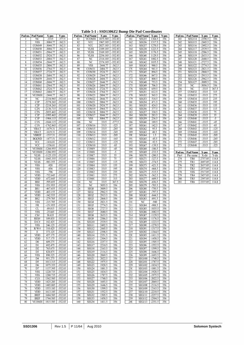
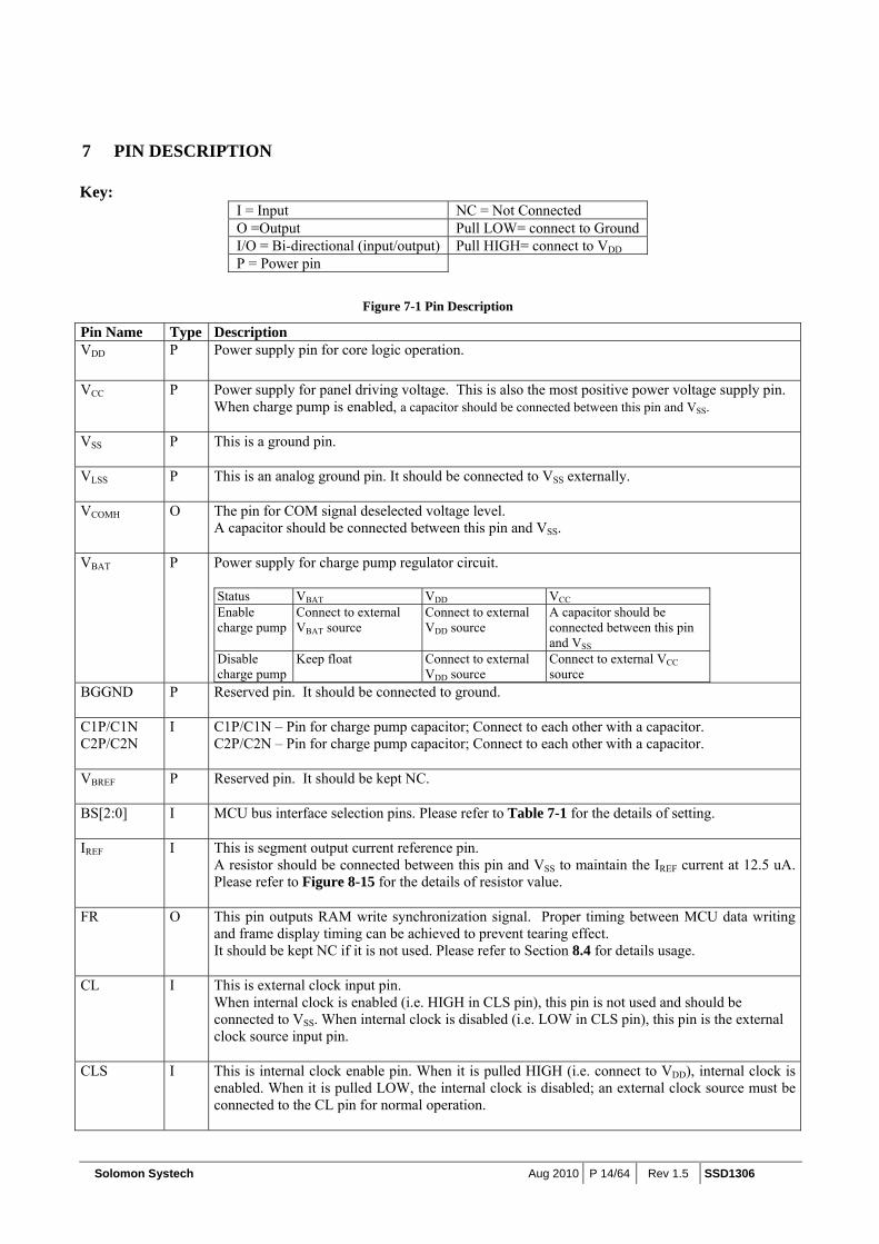
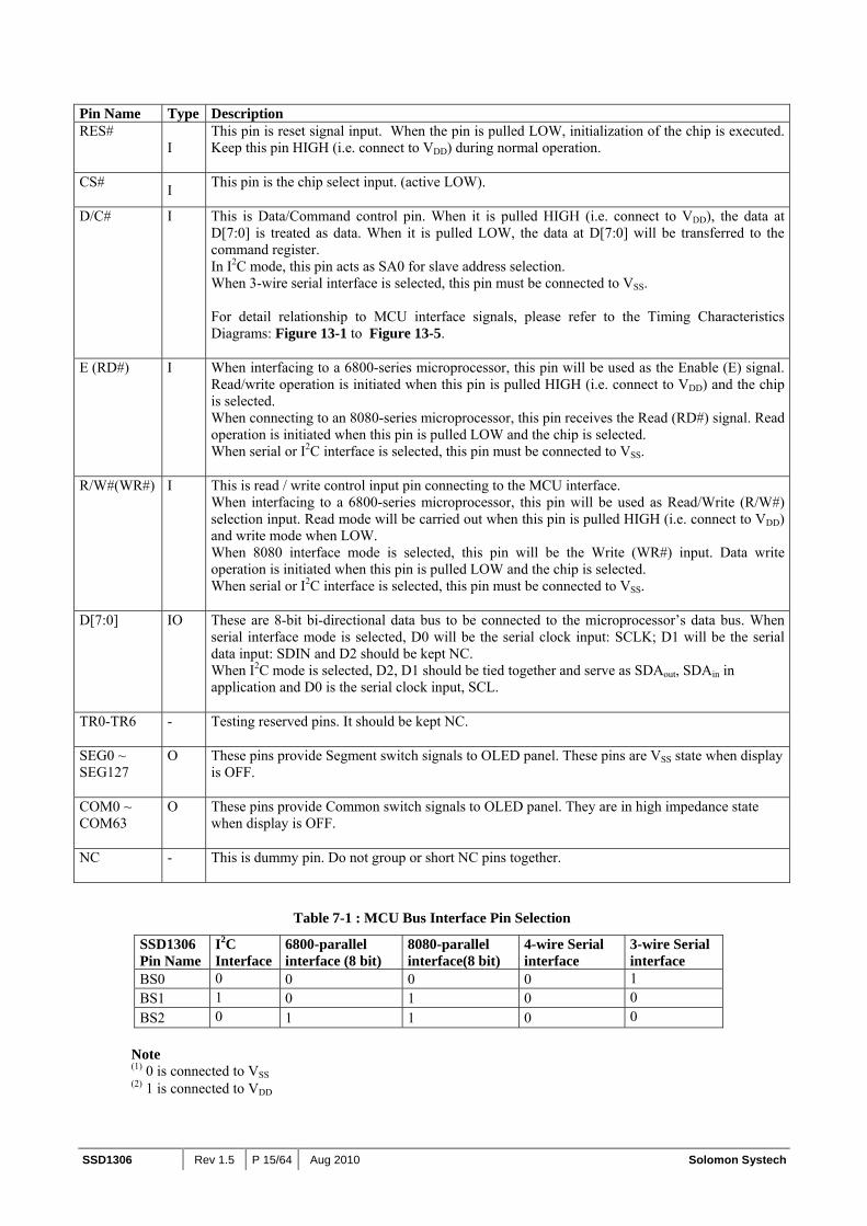
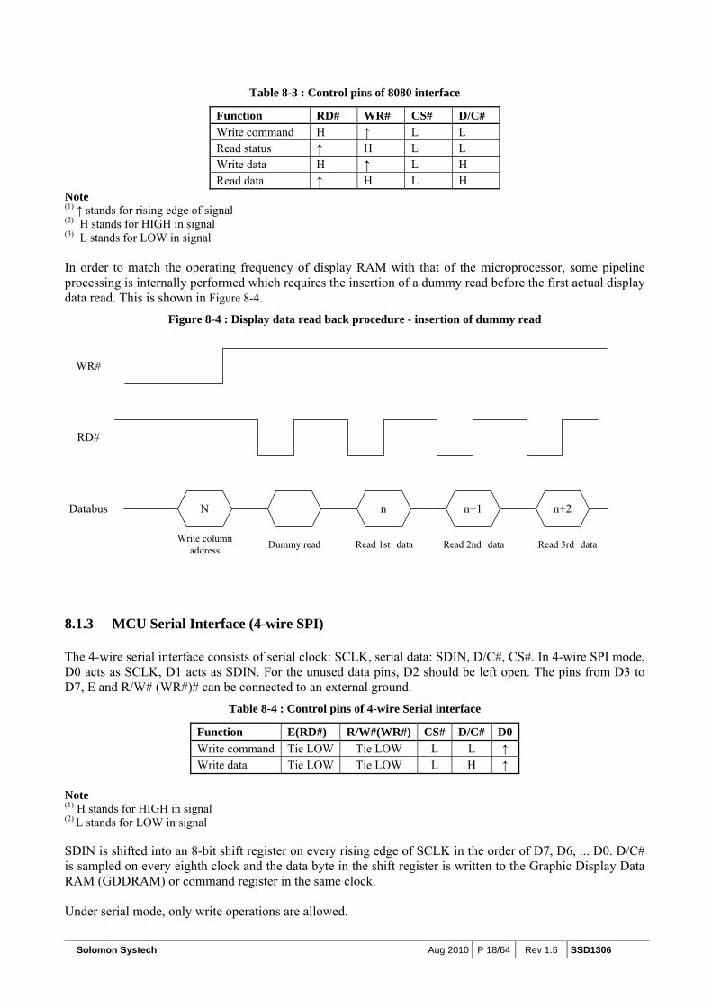
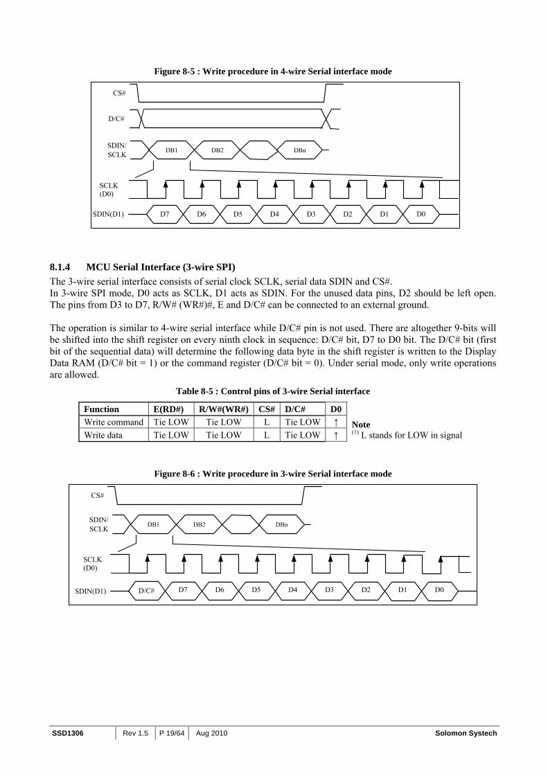
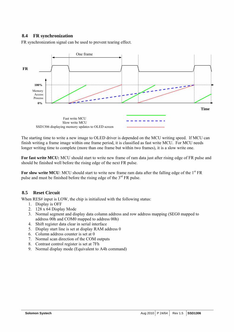
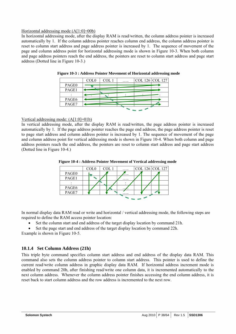
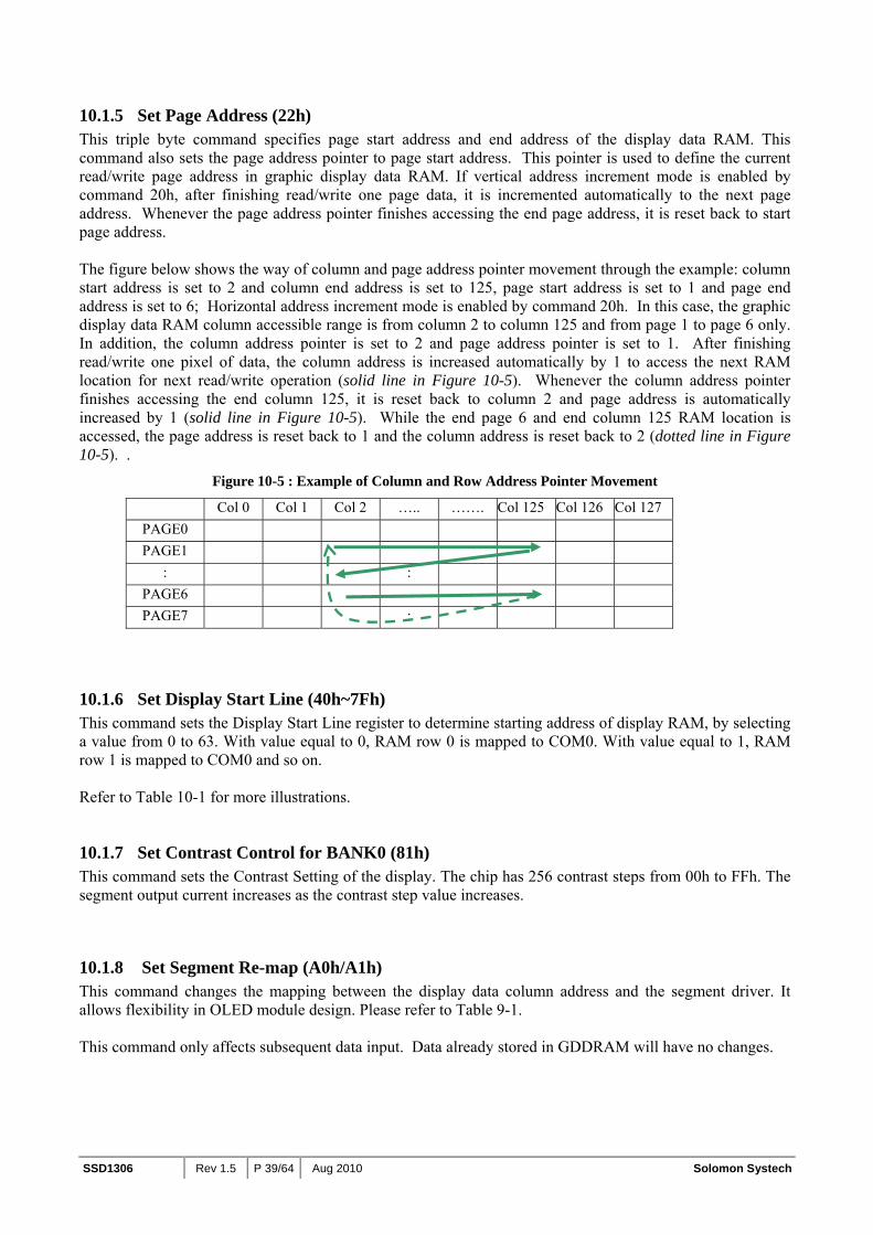
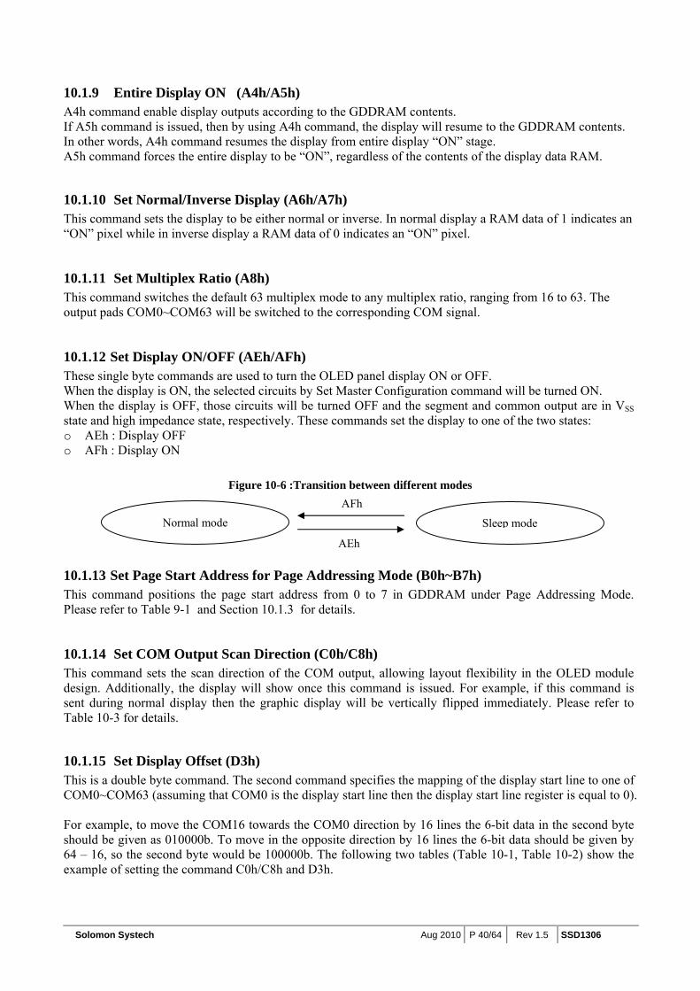
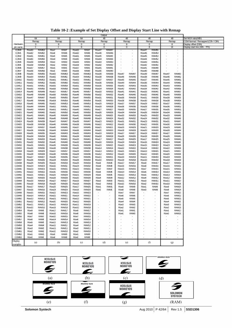
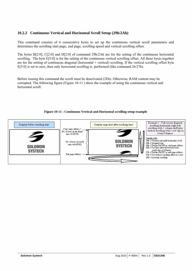
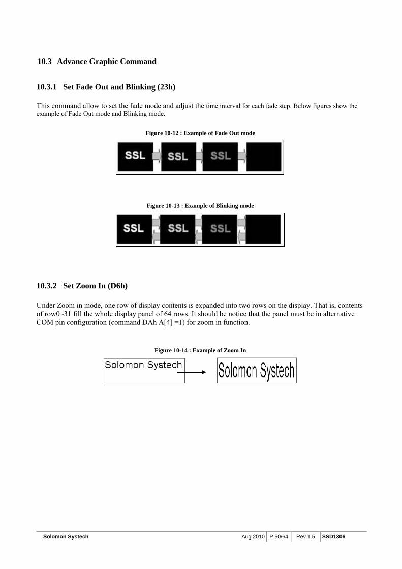
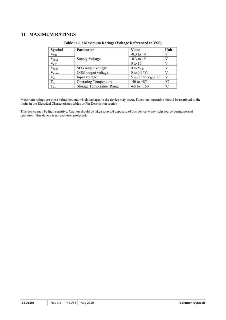
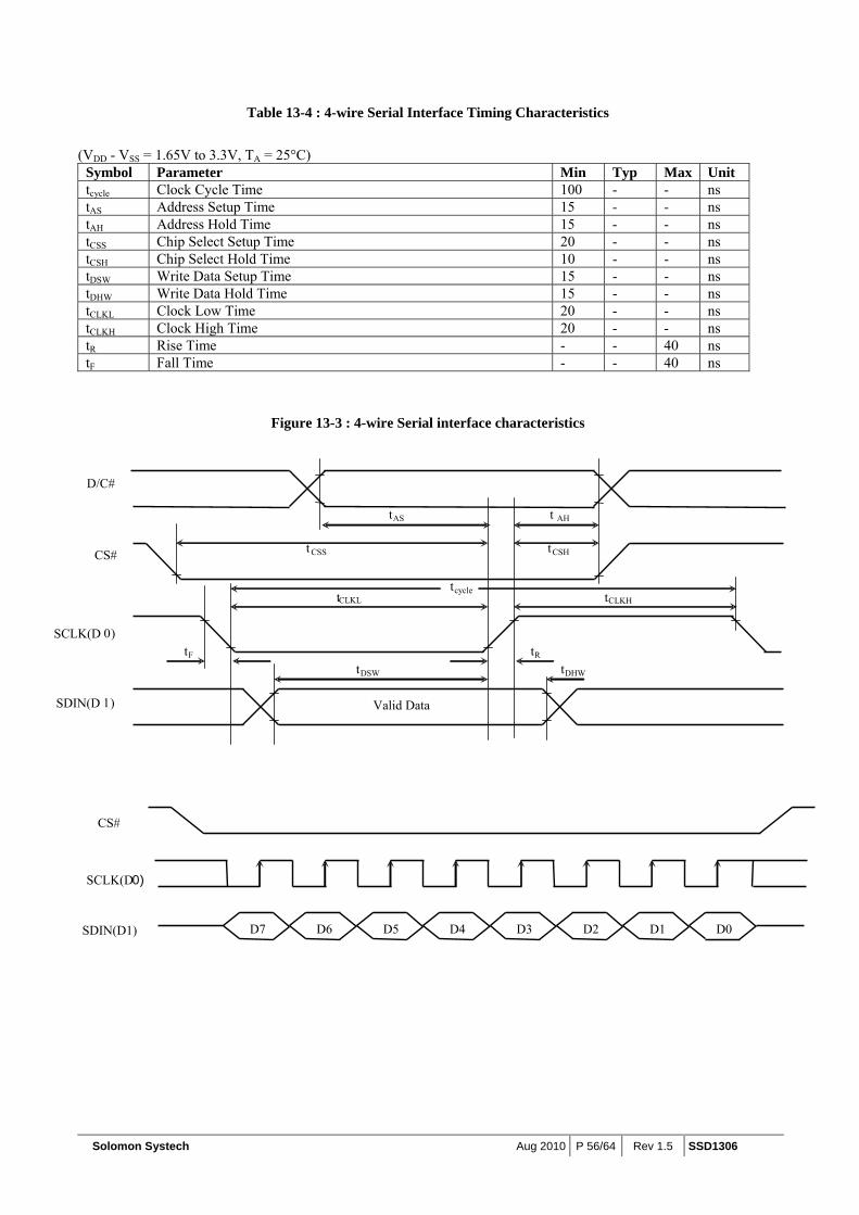
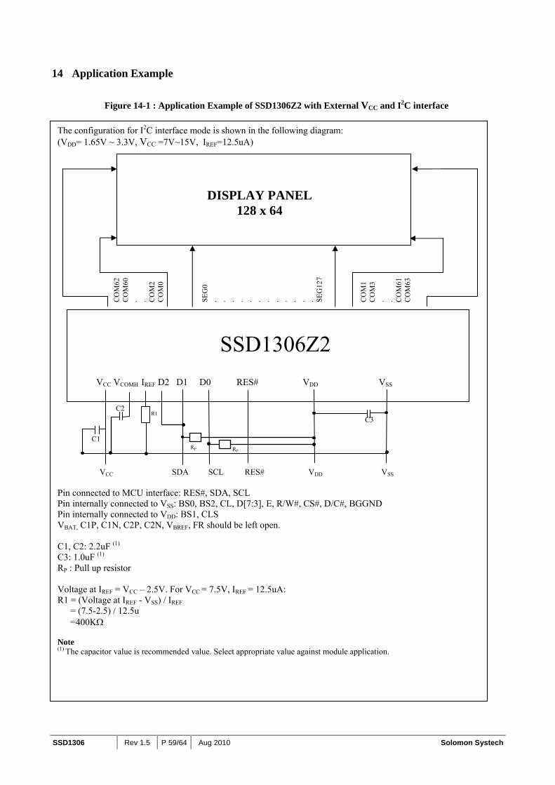