SSB RADIOTELEPHONE - ingelmar.cl Service Manual A.pdf · specifications conform to the FCC...
136
SSB RADIOTELEPHONE MODEL FS-1503
Transcript of SSB RADIOTELEPHONE - ingelmar.cl Service Manual A.pdf · specifications conform to the FCC...

SSB RADIOTELEPHONE
MODEL FS-1503

F I R S T E D I T I O N : A U G 1 9 9 8
Yo u r L o c a l A g e n t / D e a l e rFURUNO E L E C T R I C C O., LT D.c
9 - 5 2 , A s h i h a r a - c h o ,N i s h i n o m i y a , J a p a n 6 6 2
Te l e p h o n e : 0 7 9 8 - 6 5 - 2 1 1 1Te l e f a x : 0 7 9 8 - 6 5 - 4 2 0 0
A l l r i g h t s r e s e r v e d . Printed in Japan
P U B . N o . S M E - 5 6 1 4 0 - AF S - 1 5 0 3( K A O K )

i
Chapter 1 Configuration1.1 configuration..........................................................1-1
Chapter 2 Circuit Description2.1 General................................................................... 2-12.2 CPU........................................................................ 2-62.3 Oscillator................................................................ 2-132.4 TX/RX circuit......................................................... 2-172.5 Receiver Circuit...................................................... 2-212.6 Power Supply SW Circuit....................................... 2-262.7 SW REG Board (option)......................................... 2-272.8 ANT COUP (Antenna Coupler).............................. 2-282.9 Interface ................................................................. 2-34
Chapter 3 Location of Parts3.1 Main Unit ............................................................... 3-13.2 AT-1503................................................................. 3-53.3 Power Supply Unit ................................................. 3-6
Chapter 4 System Settings4.1 Changing System Settings ...................................... 4-24.2 System Channels List ............................................. 4-34.3 Channel Programming............................................ 4-84.4 Power Data Setting................................................. 4-134.5 BC Band Filter Setting ........................................... 4-184.6 Setting for NBDP (DP-6)........................................ 4-19
Chapter 5 Maintenance5.1 Periodical Checks ................................................... 5-15.2 Self-test .................................................................. 5-25.3 Troubleshooting...................................................... 5-65.4 Measurement .......................................................... 5-85.5 How to Change PA Transistor ................................ 5-115.6 Measurements and Transistor ................................. 5-125.7 Location of Parts .................................................... 5-16
Specifications _________________________________ AP1
Frequency List ________________________________ AP2
Parts List ____________________________________ D-0
Contents of Drawings __________________________ S-0
Table of Contents

1-1
1.1 Configuration
The basic FS-1503 consists of a transceiver unit (main unit) and antenna coupler (AT-1503), and covers the frequency range 1.6 to 27.5 MHz.
AT-1503
(Antenna coupler)
FS-1503
PC-220
(DC-DC CONV)
DB-500
(Distributor)
100/110 200/220
VAC
24 VDC
DSC-6
(DSC Terminal)
NBDP
MF/HF RT
DP-6
(NBDP Terminal)
MF/HF RT
DSC
COUPLER
REMOTE
CONTROL
13.6 VDC
MIC30 A
DSC
MF/HF RT
AA-50
(MF/HF WR)
Rem 1
Rem 2 Rem 3 Rem 4 Rem 5
MIC/HANDSET
SP
MF/HF RT orRECEIVER
ANT
TB1 TB2
TB3
ANT
Data transfer unit
or DB-120(Distributor)
Note)
1) Max. two DB-1202) No DB-500
connected to DB-120
PR-270(AC Rec.)
· BK ±12 V· TX KEYED· RX MUTE· GND
RB-500
(Remote station)
Figure 1-1 System Diagram
Chapter 1 Configuration

1-2
1. FS-1503 Standard Supply
There are four models depending on the selection of an antenna coupler and a handset.
Specification
Antenna Coupler HandsetCode No. Model
Yes Yes 000050900 FS-1503-01
Yes No 000050901 FS-1503-02
No Yes 000050902 FS-1503-03
No No 000050903 FS-1503-04
The table below lists the complete set.
Standard Supply
Name Type Q'ty Code No. Remarks
SSB Transceiver FS-1503 1 000050905
Antenna coupler AT-1503 1 000050904
CP05-07600 1 000050906 with couplerInstallation materials
CP05-07610 1 000050907 without coupler
FP05-05000 1 000050908 with handsetAccessories
FP05-05010 1 000050909 without handset
OME-56140 1 000808223 Operator's ManualDocument
IME-56140 1 000808224 Installation Manual

1-3
2. FS-1503 Optional Supply
Optional Supply
Name Type Q'Ty Code No. Remarks
AC Power Supply PR-270 1 000113349
DC Power Supply PC-220 1 000113350
Loudspeaker MX910-X01 1 000138001
REMOTE A Kit 0P05-82 1 005939810 05P0457 (RS-232C)
REMOTE B Kit 0P05-83 1 005939820 05P0458 (Current Loop)
CONTROL Board 0P05-41 1 005920330 05P0459
Filter (0.4 kHz) SF0L04 1 000116693 For TLX
SW REG Board 0P05-84 1 005939830 For BATT floating ground
Handset HS-6000FZ5 1 000112623
Microphone M112D 4509910 1 000116487 Noise canceling
Dummy load 0P05-85 1 005939840 05P0670
Copper band 04S0801 30x1200x0.3 1 000572187
U-Bolt 0P05-12 1 005923680 For fixing antenna
05S0949-0 L-20M 1 000130485
05S0949-0 L-30M 1 000130486
05S0949-0 L-40M 1 000130487Cable Assy
05S0949-0 L-50M 1 000130488
Control Cable betweenmain unit and antenna coupler
05S0462-1 L-20M 1 000113361
05S0462-1 L-30M 000113362
05S0462-1 L-40M 000113363Cable Assy
05S0462-1 L-50M 1 000113364
Coaxial Cable betweenmain unit and antenna coupler
Distributor DB-120 1 000057231 Two output, RB-500not connectable
Distributor DB-500-RS (E) 1 000056836 Five outputs
Remote Station RB-500 1 000054514
FAW-6D 1 000572128 With insulator
FAW-6R2 1 000572108 Welding mounting base(copper lug)
FAW-6RP2 1 000572109 Welding mounting base(M-type connector)
FAW-6R2A 1 000107921 Fixing to post (copper lug)
Whip antenna
FAW-6RP2A 1 000107920 Fixing to post(M-Type connector)

1-4
Optional Supply
Name Type Q'ty Code No. Remarks
E-22 1 000050632 Doublet Antenna Kit
E-24 1 000050634 Single Wire Antenna Kit
E-25 1 000050635 Doublet-span Antenna Kit
E-26 1 000050636 Whip Antenna Lead-in Kit
Antenna materials
E-27 1 000050637 Whip Antenna Feeder Kit

2-1
2.1 General
The SSB transmitter/receiver (FS-1503) has been developed as an upgraded successormodel of FS-1550 and FS-1502, which is used for pleasure boats and fishing boats. Thespecifications conform to the FCC regulations and the inspection standards of suchcountries as New Zealand, Australia, Russia, China, and southeastern Asian countries.
This model features that it uses DDS circuit for the local oscillator to reduce the frequen-cy switching time and thus enables telex communication. It has a built-in two-tone alarmand is powered by a 13.6 V supply.
The transmitter works in 1.6 MHz to 23.0 MHz, 150 Wpep and in 23.0 MHz to 27.5MHz, 75 Wpep with an automatic forced-air-cooling to PA section by FAN and the re-ceiver works in 0.1 MHz to 29.9 MHz. The antenna coupler is automatically tuned to op-erating frequencies and does not need matching operation. An optional dummy antennacan be installed in the antenna coupler.
ITU channels are standard channels. In addition, there are 199 user-programmable chan-nels and 65 station names among them can be displayed.
Chapter 2 Circuit Description

2-2
1. Interconnections
PA/FIL (05P0667)
COUP (05P0669)
DUMMY · DUMMY CONT (05P0670)
· DUMMY (10 Ω + 250 pF)
CPU (05P0665)
(CPU/LCD/KEY)
TX/RX (05P0666)
CONT (05P0459)
REMOTE-A/B (05P0457/8)
SW.REG (05P0668)(option)
RFCONT
FREQ/CH
SP
BK
REMOTE
TX
RXPA IN
RX OUTPA ON
TEMP
ALC
RF
BK ON
CLK, ST, DATA
12 V
ANT
13.6 V
13.0 V
13.6 V
30 A
12 V
TUNE, BUSY, THROU DUMMY, 12 V
CHK EXC, DDS DATA/CLK, RX, MUTE, TX KEY, TXD, RXD, TX KEYED
PTT, T/R, MUTE, SQ SIG, S, TONE, EXC ON, PA ON, BK ON, RF, ST FIL, ST TX/RX, CLK, DATA, PLL1 ENB, PLL3 ENB, DDS LOAD, ST SYN, UNLOCK, TEMP, ALC REF, FAN
TD/RD, LINE IN/OUT, TX KEY, RX MUTE
TX KEYED, RX MUTE, BK+/-
MIC
(option)
AT-1503
FS-1503
ANT
GND
13.6 V
Figure 2-1 Interconnection Diagram

2-3
2. Function of PCB
Table 2-1 Function of PCB
Board Name Type Description Remarks
FS-1503
CPU 05P0665Scans the key switches, outputs signalsto the LCD-panel display, and controlseach circuit block (input/output control).
TX/RX 05P0666
Comprises a modulator for microphoneand LINE input signals, a transmittingRF amplifier, a receiving RF amplifier,low-frequency amplifiers, and a synthe-sizer (DDS) circuit.
TLX FIL(optional)
NB DET 05P0466 Includes a noise blanking control circuit.
REMOTE (A) 05P0457 Equipped for remote control of DSC,RB-500, and NBDP.
OPTION(RS-232C)
REMOTE (B) 05P0458 Equipped for remote control of RB-500. OPTION(Current Loop)
CONTROL 05P0459 Equipped when BK and MUTE signalsare needed to interconnect receivers.
OPTION
PA/FIL 05P0667
Comprises the power input relay section,PA section, and TX-FIL section. Therelay section contains a power ON/OFFcircuit by a power input-line relay, and aprotection circuit against over-voltageand over-current. The PA section in-cludes a transmitting high-frequencypower amplifier circuit and a tempera-ture detecting circuit. The TX-FIL secti-on contains transmitting LPF,ALC/reflection detecting circuit, and atransmitter/receiver switching circuit.
BC BAND FILSetting
SW REG 05P0668Equipped to change the grounding of theunit from negative ground to floatingground.
OPTION
AT-1503
COUP 05P0669
The automatic tuning circuit in whichCPU controls L/C matching network bydetecting the phase, SWR, and frequencyof the RF input signal from the mainunit. The input/output signals are TUNE,BUSY, and THROU. The input imped-ance is 50 Ω and the maximum inputpower is 150 Wpep.
Selftest functionwith JP-1 set to"SELF TEST"
DUMMY CONT 05P0670Controls ON/OFF of the dummy antennaof 10 Ω + 250 pF, 100 W.
OPTION
Note) TX/RX board is equipped with CONTROL board (option), REMOTE-(A) or -(B)board (options), and NB-DET board. REMOTE-(A) or -(B) board is selected accordingto the used remote-control specification, RS-232C or current-loop, respectively.

2-4
3. Spectrum
1.5
455
456.5
54000
54455
F
F + 1.5
F + 54456.5
1.5
kH
z
45
5 k
Hz
54
45
5 k
Hz
TX
1st
mo
d./
RX
3rd
co
nv.
TX
2n
d m
od
./R
X 2
nd
co
nv.
TX
3rd
mo
d./
RX
1st
co
nv.
TX
sig
na
l
(3Lo)
(2Lo)
(1Lo)
1.5
455
456.5
54000
54455
F
F + 1.5
F + 54456.5
RX
sig
na
l
(3Lo)
(2Lo)
(1Lo)
kHz kHzJ3
E T
X
J3E
RX
1.5
455
456.5
54000
54455
F
F + 1.5
F + 54456.5
TX
sig
na
l
(3Lo)
(2Lo)
(1Lo)
1.5
455
456.5
54000
54455F
F + 1.5
F + 54455
RX
sig
na
l
(2Lo)
(1Lo)
kHz kHz
H3E
TX
H3E
RX
Ca
rrie
r a
dd
ed
F - 1.5
453.5
54456.5
54453.5
54456.5

2-5
1.7
455
456.7
54000
54455
F
F + 54455
1.7
kH
z
45
5 k
Hz
54
45
5 k
Hz
TX
1st
mo
d./
RX
3rd
co
nv.
TX
2n
d m
od
./R
X 2
nd
co
nv.
TX
3rd
mo
d./
RX
1st
co
nv.
TX
sig
na
l
(3Lo)
(2Lo)
(1Lo)
1.7
455
456.7
54000
54455
F
F + 54455
RX
sig
na
l
(3Lo)
(2Lo)
(1Lo)
kHz kHz
J2B
RX
J2B
TX
YB
17
00
± 8
5 H
z
YB
YB
YB
YB
YB
YB
YB
YB
YB
YB 1.9
455
456.9
54000
54455
F
F + 54455
RX
sig
na
l
(3Lo)
(2Lo)
(1Lo)
kHz
F3
C R
X
19
00
± 4
00
Hz
BW
BW
BW
BW
1.9
kH
z

2-6
2.2 CPU
1. General
LCD PANEL U1: 05S0805
LCD DRIV U2: HD61602
KEY PAD
LED DRIVEEROM U5: X24C16S
Analog signal Detected
Serial data (converted to parallel data on each PCB.)
Input/output control signal
CR1: BlinkingCPU: U6 HD6475328F10
(H8/532one-time)
or
HD6435328F
(H8/532maskROM)
CPU ROM RAM A/D I/O
TX/RX DATA (REMOTE CONT)
DATA, CLK, ST, ENB
S, IA, RF, TEMP, CHK EXC
Y1 20 MHz
TX/RX DATA
(IA not provided on standard set)
Figure 2-2 Block Diagram of CPU
U6: CPU is a 16-bit single-chip microcomputer with integrated peripheral functions suchas RAM, ROM, timer, serial I/O, A/D converter, and I/O ports. The system program,ITU frequency table, system settings, initial values of power data, etc. are stored inthe ROM of the CPU. EEROM U5: X24C16S (16 kB) stores set power data, userchannels, system settings, and key settings.
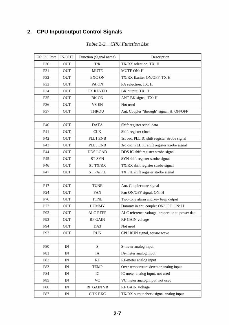
Refer to the next page for the functions of input/output control signals of the CPU.
Note) U6 is soldered to the board.
⋅ HD6475328F10 (H8/532: one-time)⋅ HD6435328F (H8/532: mask ROM) ----- for permanent use
* Program number: 05501-91-00X(This number can be confirmed by turning on power while depressing [ENT]key, and pressing any key.)
2-7
2. CPU Input/output Control Signals
Table 2-2 CPU Function List
U6: I/O Port IN/OUT Function (Signal name) Description
P30 OUT T/R TX/RX selection, TX: H
P31 OUT MUTE MUTE ON: H
P32 OUT EXC ON TX/RX Exciter ON/OFF, TX:H
P33 OUT PA ON PA selection, TX: H
P34 OUT TX KEYED BK output, TX: H
P35 OUT BK ON ANT BK signal, TX: H
P36 OUT VS EN Not used
P37 OUT THROU Ant. Coupler "through" signal, H: ON/OFF
P40 OUT DATA Shift register serial data
P41 OUT CLK Shift register clock
P42 OUT PLL1 ENB 1st osc. PLL IC shift register strobe signal
P43 OUT PLL3 ENB 3rd osc. PLL IC shift register strobe signal
P44 OUT DDS LOAD DDS IC shift register strobe signal
P45 OUT ST SYN SYN shift register strobe signal
P46 OUT ST TX/RX TX/RX shift register strobe signal
P47 OUT ST PA/FIL TX FIL shift register strobe signal
P17 OUT TUNE Ant. Coupler tune signal
P24 OUT FAN Fan ON/OFF signal, ON: H
P76 OUT TONE Two-tone alarm and key beep output
P77 OUT DUMMY Dummy in ant. coupler ON/OFF, ON: H
P92 OUT ALC REFF ALC reference voltage, propertion to power data
P93 OUT RF GAIN RF GAIN voltage
P94 OUT DA3 Not used
P97 OUT RUN CPU RUN signal, square wave
P80 IN S S-meter analog input
P81 IN IA IA-meter analog input
P82 IN RF RF-meter analog input
P83 IN TEMP Over temperature detector analog input
P84 IN IC IC meter analog input, not used
P85 IN VC VC meter analog input, not used
P86 IN RF GAIN VR RF GAIN Voltage
P87 IN CHK EXC TX/RX output check signal analog input

2-8
U6: I/O Port IN/OUT Function (Signal name) Description
P15 IN TX KEY Remote terminal TX signal, TX: L
P16 IN BUSY (TUNE OK) Busy signal from ant. coupler
P12 IN PTT PTT signal, ON: L
P73 IN RX MUTE MUTE signal from CONTROL terminal
P74 IN UNLOCK PLL unlock, unlock: L
P75 IN SQ SIG Squelch ON/OFF signal
P90 OUT DDS DATA DDS shift register serial data
P91 OUT DDS CLK DDS shift register clock
P95 OUT TXD Data to remote terminal
P96 IN RXD Data from remote terminal
P10 IN UP Freq./channel up signal
P11 IN DOWN Freq./channel down signal
P50 OUT D0 LCD data, key scan
P51 OUT D1 LCD data, key scan
P52 OUT D2 LCD data, key scan
P53 OUT D3 LCD data, key scan
P54 OUT D4 LCD data
P55 OUT D5 LCD data
P56 OUT D6 LCD data
P57 OUT D7 LCD data
P60 IN READY LCD control
P61 OUT CS LCD control
P62 OUT WE LCD control
P63 OUT SYNC LCD control
P20 IN S1 to S4 Scan input
P21 IN S5 to S8 Scan input
P22 IN S9 to S12 Scan input
P23 IN S13 to S16 Scan input
P70 OUT DIM LCD, KEY illumination
P71 OUT DIM LCD, KEY illumination
P72 OUT DIM LCD, KEY illumination
P14 IN/OUT S-DATA Serial data input/output
P13 OUT S-CLK EE-ROM clock

2-9
3. Control Signals
There are two ways for the CPU to control the transmitting/receiving circuits. One is, theCPU directly sends signals to them, and the other is, the CPU sends serial data to eachcircuit board and there the data are converted to parallel data that controls each circuit.
The CPU controls TX/RX board and PA/FIL board by sending serial-data from P40:DATA, and DDS circuit in TX/RX from P90: DDS DATA.
P40 DATAP41P46
CLKST TX/RX
P47 ST PA/FIL
P45P42P43
P90P91P44
DDS CLKDDS DATA
DDS LOAD
LOA
D
S.D
AT
A
S.C
LKST SYNPLL 1 ENBPLL 3 ENB
T So
ut
Sin
L T So
ut
Sin
L T So
ut
Sin
L
T So
ut
Sin
L CLK
LD
EN
B
Din
CLK
LD
EN
B
Din
Q1 2 3 4 5 6 7 8
SP
OF
F
RX
AF
OF
FM
IC&
TO
NE
LIN
E O
NM
IC O
N-6
dB
NB
OF
FT
ES
T
Q1 2 3 4 5 6 7 8
INT
ER
CO
M
AG
C O
FF
AG
C F
AS
TR
X H
3E
TX
H3
EF
IL W
FIL
NF
IL M
Q1 2 3 4 5 6 7 8
LP
F 6
LP
F 5
LP
F 4
LP
F 3
LP
F 2
LP
F 1
Q1 2 3 4 5 6 7 8
BA
MD
1B
AN
D 2
BA
ND
3B
AN
D 4
H/L
DD
S R
ES
ET
(DDS)
U503 U502 U504(3Lo)(1Lo)(1Lo)
U501
• U11 (M54972FP) • U12 (M54972FP) • U501 (AD7008AP20) • U502 (MC145170D1) • U503 (M54972FP) • U504 (MC145170D1)
U11U12
U7 (M54972P)
PA/FIL (05P0667)TX/RX (05P0666)
U6
CPU (05P0665)
HD6475328F10 or HD6435328F
Figure 2-3 Serial Data Lines
Serial-data transmission has an advantage of smaller number of control lines than paral-lel-data transmission. However, the signals T/R, MUTE, EXC ON, PA ON, TX KEYED,and BK ON are directly sent as parallel data from CPU, because these signals need pre-cisely matched timing with their object circuits.
Whereas DATA CLK for the serial-data is periodically sent from the CPU, ST (LATCH)signal is sent to control the circuit (M54972P) when the data are changed by key opera-tions.
The transmission timing of the serial-data is shown in Figure 2-4 and the functions of theserial control signals are listed on Table 2-3.

2-10
Serial-data
CLK
LATCH (ST)
While data and clock are sent from CPU, changed data is taken in by LATCH signal.
Figure 2-4 Transmission Timing
M54972P (8BIT SERIAL INPUT LATCHED DRIVER)
Q
LD
D Q
T
EN Enable input
LATCH Latch input
Sin Serial data input
T clock
O1
S out serial output
Q
LD
D Q
T
O2
Q
LD
D Q
T
O3
Q
LD
D Q
T
O4
Q
LD
D Q
T
O5
Q
LD
D Q
T
O6
Q
LD
D Q
T
O7
Q
LD
D Q
T
O8
Vcc power P-GND
Driver GND
4
7
6
2
1
3
16 15 14 13 10 9
5
8
12 11
Figure 2-5 Block Diagram of M54972P
M54972P consists of 8 D-flip-flops and 8 latches connected to the outputs of the flip-flops. Serial-data signals input to the serial-data input (S-in) and clock pulses input to theclock input (T). Every time the clock changes from L to H, the input signal is taken in theinternal shift register and the data in the shift register shifts successively.
The serial output (S-out) is connected to the serial input (S-in) of the next M54972P,when more than one M54972P are connected in series to increase bit number.
The data in the shift register output to the parallel output Q1 to Q8, when the latch input(LATCH) is H, the enable input for output control (EN) is L, and the clock changes fromL to H.

2-11
Table 2-3 TX/RX Serial Data List
IC NC
U11
U22
OU
T
NC
BIT
Q8
Q7
Q6
Q5
Q4
Q3
Q2
Q1
Q8
Q7
Q6
Q5
Q4
Q3
Q2
Q1
15 14 13 12 11 10 9 8 7 6 5 4 3 2 1 031 ↓
Func
tion
See
note
.
FIL
M
FIL
N
FIL
W
TX
H3E
RX
H3E
AG
C F
AST
AG
C O
FF
INT
ER
CO
M
TE
ST
NB
OFF
-6 d
B
MIC
ON
LIN
E O
N
MIC
& T
ON
E
RX
AF
OFF
SP O
FF
MU
TE
0 0 1 0 1 0 0 1 1 - 0 0 0 0 1 1
OFF
Def
ault
2182
kH
zH
3EL
SBU
SBH
3ET
LX
TL
XFA
X
1 0 0 0 0 0 - 1 1 - 0 0 0 0 1 -
OFF
1 0 0 0 0 0 - 1 1 - 0 0 0 0 1 -
OFF
0 0 1 0 1 0 - 1 1 - 0 0 0 0 1 -
OFF
1 (0
)
0 (1
)
0 0 0 1 - 1 1 1 0 0 0 0 1 -
OFF
1 0 0 0 0 0 - 1 1 - 0 0 0 0 1 -
OFF
1 0 0 0 1 0 1 1 1 - 0 1 0 1 1 0 ON
1 0 0 0 1 0 1 1 1 - 0 1 0 1 1 0 ON
1 0 0 1 1 0 1 1 1 - 1 1 0 1 1 0 ON
1 0 0 0 1 0 1 1 1 - 0 0 1 0 1 0 ON
1 0 0 0 1 0 1 1 1 - 0 0 1 0 1 0 ON
1 0 0 1 1 0 1 1 1 - 1 0 1 0 1 0 ON
1 0 0 0 1 0 1 1 1 - 0 0 1 0 1 0 ON
1 0 0 0 1 0 1 1 1 - 0 0 0 1 1 1 ON
1 0 0 0 1 0 1 1 1 - 0 0 0 1 1 1 ON
1 0 0 1 1 0 1 1 1 - 1 0 0 1 1 1 ON
1 0 0 0 0 1 0 1 0 1 0 0 0 0 0 1 ON
1 0 0 0 1 0 1 1 1 1 0 0 0 1 0 1 ON
1 0 0 0 1 0 1 1 1 - 0 0 0 1 1 - ON
- - - 0 - - - 0 1 - 0 1 0 0 1 1 ON
- - - 0 - - - 0 1 - 0 0 0 0 0 - ON
RX
MIC
TX
Rem
ote
TX
(T
X K
EY
)To
ne/2
-Ton
e A
LM
Self
test
Tun
eIn
terc
om
LSB
USB
H3E
LSB
USB
H3E
LSB
USB
H3E
RX
TL
XT
XT
LX
USB
(1.5
kH
z)C
allin
g/B
usy
Res
pons
e
CPU
I/O
: P31
Not
e) B
its 1
6 to
31
are
not u
sed.
(1: H
igh,
0: L
ow)

2-12
Table 2-4 PA/FIL Serial Data List
StatusIC OUT BIT Functions
TX RX
Q8 7 LPF1 0.1 to 2.4 MHz: "L"
Q7 6 LPF2 2.4 to 3.6 MHz: "L"
Q6 5 LPF3 3.6 to 6.0 MHz: "L"
Q5 4 LPF4 6.0 to 10.0 MHz: "L"
Q4 3 LPF5 10.0 to 18.0 MHz: "L"
Q3 2 LPF6 18.0 to 30.0 MHz: "L"
Q2 1 NOT USED
U7
Q1 0 NOT USED

2-13
2.3 Oscillator
Taking J3E as an example, the outline of the frequency conversion is shown in Figure 2-6and the relation between the transmitting and receiving frequencies and local frequenciesis shown in Table 2-6.
The frequency conversion circuit and the local oscillator circuit are included in TX/RXboard.
Outline of frequency conversion on J3E
1Lo (F + 54.455 MHz + 1.5 kHz)
2Lo (54 MHz)
3Lo (456.5 kHz)
T/RX (Fo + 1.5 kHz)
AF (1.5 kHz)
54.455 MHz 455 kHz
DDS PLL 1
1/2
PLL 3 1/100
36MHz
Ref. OSC
1 Lo
2 Lo
3 Lo
Ref.
Figure 2-6 Frequency Conversion
Table 2-5 Frequency of Local oscillator
Mode 1st Local oscillator (1Lo) 2nd Local oscillator(2Lo)
3rd Local oscillator(3Lo)
USB F + 54.455 MHz + 1.5 kHz 54 MHz 456.5 kHz
LSB F + 54.455 MHz - 1.5 kHz 54 MHz 453.5 kHz
TX F + 54.455 MHz + 1.5 kHz 54 MHz TX 456.5 kHzH3E
RX F + 54.455 MHz ± 0 kHz 54 MHz RX 455 kHz
TLX F + 54.455 MHz ± 0 kHz 54 MHz 456.7 kHz
FAX F + 54.455 MHz ± 0 kHz 54 MHz 456.7 kHz

2-14
Lo
op
Filt
er
VC
O
Re
f. O
SC
36
MH
z
(Ba
nd
se
lect
ion )
DD
S
Co
mp
. D
ivid
er
(N =
54
to
84
)
Re
f. D
ivid
er
(
M =
6)
Ph
ase
C
om
pa
rato
r
FL
50
2 6
MH
z
1/2
LAT
CH
C55
4
U50
6O
VE
N
S.D
AT
AS
.CL
K
U50
1 (A
D70
08A
P20
)
1L
o
2L
o
3L
o
Fo
= F
+ 5
4.4
55
M +
OF
F S
ET
54
M
45
3.5
to
45
6.9
kH
z
(54.
555
to 8
4.45
499
MH
z)
U50
3
Fro
m C
PU
LD
CLKPLL1 ENB
DATA
Un
lock
(S
ee
no
te)
U50
2
18 M
Hz
1
MH
zQ
501-
2
4 ×
2 ??
Ou
tpu
t o
f D
DS
is u
sed
as
a r
efe
ren
ce f
req
ue
ncy
of
PL
L.
Fre
qu
en
cy d
ata
ch
an
ge
s th
e r
efe
ren
ce f
req
ue
ncy
to
pro
du
ce 1
Lo
si
gn
al.
(6 M
Hz:
DD
S O
utp
ut
Fre
q.)
× N
1
Lo
Fre
q.
=M
Fre
q.
Da
ta
VC
O B
AN
D d
ata
No
te)
Wh
en
th
e C
PU
re
ceiv
es
"Un
lock
" S
ign
al f
rom
PL
L I
C U
50
2 o
r U
50
4,
T
X a
nd
RX
are
dis
ab
led
an
d f
req
ue
ncy
ind
ica
tion
blin
ks.
Ph
ase
A
ccu
mu
lato
rR
OM
L
oo
k-u
p T
ab
leD
/AF
IL
Re
f. C
LK
Fre
q.
Se
lect
Da
ta
OU
TP
UT
Sim
plif
ied
DD
S B
lock
Dia
gra
m
LOA
D
FL
50
1
Lo
op
Filt
er
VC
O
Co
mp
. D
ivid
er
(N =
45
35
to
45
69
)
Re
f. D
ivid
er
(M =
18
00
)P
ha
se
Co
mp
ara
tor
10 k
Hz
C5
39
/R5
37
DATA
LD
CLKPLL3 ENB
CLKST SYN
DATA
Q1
to
5
U50
4
1/1
00
U50
5
Fre
q. A
djus
ter
Q51
6
Y50
1Q
510
to 5
12
Q51
3
Q50
8
TP
50
6
(6
MH
z)
TP
50
7T
P5
02
TP
50
5
TP
50
3
U50
7/Q
515
12V
Q50
9
* D
ep
en
din
g o
n c
lass
of
em
issi
on
* D
ep
en
din
g o
n c
lass
of
em
issi
on
S.D
AT
AS
.CL
KLO
AD
CLK
PLL
1 E
NB
DA
TA
ST
SY
N
PLL
3 E
NB
(18
MH
z)
(36
MH
z)
(MC
1451
70D
1)
(MC
1451
70D
1)
(M54
972)(M
5445
9L)
(MB
511)
(6
MH
z)
DD
S R
ES
ET
Q6
DD
S R
ES
ET
Q50
6
Q50
5
Figure 2-7 Block Diagram of Synthesizer Circuit

2-15
3rd Local Frequency (3Lo)
3Lo is generated by PLL3 (U504). The oscillating frequency varies in accordance withthe class of emission. For example, 456.5 kHz is for J3E (USB) and 456.7 kHz for J2B(TLX).
2nd Local Frequency (2Lo)
2Lo, 54 MHz, is generated by mixing the output of a reference oscillator (Y501), 36MHz, with one half of the frequency, 18 MHz.
1st Local Frequency (1Lo)
1Lo is generated by PLL (U502) and DDS (U501). The output frequency is "the set fre-quency + 54.455 MHz + the offset frequency".
The frequency is generated by varying the reference frequency and the frequency divi-sion ratio of PLL in accordance with the set value of the frequency — the reference fre-quency of PLL is the output frequency of DDS (Direct Digital Synthesizer). The relationbetween the output frequency of DDS and the oscillating frequency of PLL is as follows.
DDS output frequency, fo = (K × fc) ÷ 2N,
where fc is DDS clock frequency (18 MHz) → the reference frequency 36 MHz isdivided into 1/2,
N is DDS phase accumulator bit number (32 bits), and
K is DDS phase data input (32 bits) → frequency data from CPU.
PLL oscillating frequency, 1Lo = (DDS output frequency, fo × N) ÷ M,
Where N is the dividing value of the comparing frequency divider (54 to 84) →frequency data from CPU, and
M is the dividing value of the reference frequency divider (fixed to 6).
PLL (VCO) has to oscillate in 54.555 MHz to 84.45499 MHz with the set frequencies of0.1 MHz to 29.99999 MHz. One VCO with a fixed inductance coil can not cover thewide frequency range of about 30 MHz. To cover the wide range, the VCO has four coilswith different inductance and selects one corresponding to the set frequency from them.Further, the two capacitors are switched each other in combination with each coil induc-tance.

2-16
T
C
CR
50
5
CR
50
6C
R5
08
CR
50
7
C
C
C
Q503
12 V
VCO OUT
VCO CONT
R5
19
R5
20
R522
H/L (Changing capacitance)
(L)C
(C1) (C2)
(C4)(C3)
T501 - 504 BAND Select
(f VCO)
f VCO =
(C1 + C2) + (C3 + C4)
(C1 + C2) × (C3 + C4)L ×2 π
1
Note) · C2, C4 Variable with H/L Signal · C1, C3 Variable with VCO CONT
T501 - 504
· C = 1000 pF · CR506 to 508 = 1SV232 (Variable capacity diode)
Figure 2-8 1Lo PLL VCO
Table 2-6 Oscillation Frequency on Each Band
Band Set Frequency VCO Output Frequency
1-L 0.1 to 2.99999 MHz 54.55500 to 57.45499 MHz
1-H 3.0 to 5.99999 MHz 57.45500 to 60.45499 MHz
2-L 6.0 to 9.49999 MHz 60.45500 to 63.95499 MHz
2-H 9.5 to 13.49999 MHz 63.95500 to 67.95499 MHz
3-L 13.5 to 17.49999 MHz 67.95500 to 71.95499 MHz
3-H 17.5 to 21.49999 MHz 71.95500 to 75.95499 MHz
4-L 21.5 to 25.49999 MHz 75.95500 to 79.95499 MHz
4-H 25.5 to 29.99999 MHz 79.95500 to 84.45499 MHz
Note) The above table shows the VCO output frequency on TLX and FAX modes. Add anoffset frequency for other modes.
Reference) PLL1, PLL3, DDS and BAND data are set in the following order every timeset frequency and/or class of emission is changed.
1) DDS data setting2) PLL1 data setting3) SYN shift register data setting (1Lo Band data)4) PLL3 data setting

2-17
2.4 TX/RX circuit
TX/RX section (J3E)
The AF input signal from a dynamic microphone (600 Ω, rated input -46 dBm) is ampli-fied by a compressor amplifier U14 (M51304L) to increase the average transmittingpower and to suppress an over-input as well.
At the next stage U5 2/2, the AF signal gain is adjusted in accordance with the radiowave format J3E and H3E.
Further, after passing through R156 [TX GAIN], the signal is mixed with 3Lo (456.5kHz) by a ring modulator CR22 (SMS3926-023) and converted to a signal of 456.5 kHz± AF (1.5 kHz).
This signal passes through a crystal filter FL2 (2.4 kHz) and derives the first IF signal of455 kHz.
Note) The passing filter is changed according to the class of emission.
FIL 2 (fB = 2.4 kHz) J3E, H3EFIL 3 (fB = 0.4 kHz) J2B (TLX) ---- optionFIL 4 (fB = 6 kHz) H3E receiving
With H3E, 3Lo signal (456.5 kHz) is added to the output signal from FL2 (2.4 kHz)through R101 [H3E CARR].
LIM
CR27 -30
FL2
2.4 kFL3
FL4
6.0 k
0.4 k
MIC
LINETONE
MIC
ON
MIC
&T
ON
E
TP6
U5 2/2
R156
INTERCOM
-6 d
B (
H3
E)
3Lo (456.5 kHz)
CR22
Q16U14
COMP
TX
TP5
R101
H3E CARR
TX GAIN(600 Ω – 46 dBm)
FIL
N/M
/W455 kHz
Figure 2-9 AF Amplifier thru 455 kHz Circuit
The signal of 455 kHz is mixed with 2Lo (54 MHz) by a ring modulator CR10(SMS3926-023) and converted to a signal of 54 MHz ± 455 kHz. This signal is amplifiedby Q7, passed through a filter FL1 (54.455 MHz), and derives the second IF signal.
This signal of 54.455 MHz is mixed with a local oscillator signal 1Lo (F + 54.455 MHz +1.5 kHz) by DBM CR5 (SBL-1C) and converted to a signal with frequency (F + 54.455MHz + 1.5 kHz) ± 54.455 MHz. This signal further passes through 30 MHz L.P.F. andderives a transmitting signal with a frequency of F + 1.5 kHz.
Note) The output impedance is matched to 50 Ω over the wide frequency range by in-corporating the 30 MHz L.P.P and 60 MHz H.P.F. to the output of DBM CR5, reducingspurious signals generated in the DBM.

2-18
ALC (From PA/FIL PCB)
ALC
FL1
U7/8
ALC
BLA
NK
TP3
CR5
U6
54.455 MHz
2Lo (54 MHz)
CR11 -12
NB
CR24
F + 1.5 kHz455 kHzCR10
Q7
30M L.P.F
1Lo (F + 54.455 MHz + offset:1.5 kHz)
TP1
60M H.P.F
Q26 Q25
ALC REF (From CPU: Power data)
(MC1350D)
CHK EXC
(To PA/FIL PCB)
(RF DET)
(Power CONT)
Figure 2-10 455 kHz Circuit thru Exciter
The power of this transmitting signal is adjusted in a gain-control IF amplifier U6(MC1350D), which is controlled by the ALC circuit that consists of U7 and U8.
The input signals to the ALC circuit are the power data (ALC REF) at CPU board and afeedback signal of transmitting power detected at the output of the FIL section on PA/FILboard. That is, the transmitter output level of TX/RX board is automatically adjusted soas to derive the transmitting power set by the power data.
This transmitting signal outputs to PA/FIL board after passing through amplifiers Q26and Q25.
The transmitting power signal of TX/RX board is detected by CR24, C103, and R112(self-check signal) and input to CPU as CHK EXC signal.
The transmitting power is self-checked in a condition; 3 MHz, J2B, 1700-Hz tone signaland a power data of 255.
Reference) When a transmitting power is 140 W to 150 W, CHK EXC level is 2.4 to 2.6 V.
PA/FIL section
The transmitting output signal from TX/RX board (EXC OUT) inputs to PA/FIL board. Itis passed through a π-type attenuater (-1.5 dB) that consists of R14 to R16, amplified bya two-stage push-pull amplifier, and sent to FIL section. The gain in the PA section isabout 25 dB, and the loss in the FIL section is less than 0.5 dB.
In transmitting, the gain of the PA circuit is controlled by switching ON/OFF the biasvoltage of the two-stage push-pull amplifier in accordance with PA ON signal from CPU.The bias voltage for Q4 and Q5 is 40 to 60 mV across R69.
For Q6 and Q7, the current flowing through FL3 is adjusted to 500 ± 50 mA by R39[BIAS].
To protect the PA circuit, a thermister RT2 detects the temperature of PA transistors. If itdetects a temperature of 90 to 100 °C, the power data is automatically decreased to alower set value (LOW) and prevents PA transistors from being damaged. When it detects45 °C, fan automatically air-cools the PA section.
The voltage at J1-7 (TEMP) is 1 V ± 0.1 V at the normal temperature of 25 °C, 1.85 V at45 °C (FAN ON), and 4.1 V at 90 to 100 °C (LOW).

2-19
Note) PA amplifier is high-frequency-grounded to -13.6 V line through capacitors C49to C52.
ATT
-1.5 dB
TX/RXEXC OUT
PA OUT
13.6 V +AVR
PA BIASDRIV BIASPA ON
R39
PA BIAS
RT2
PA ON
TEMP
Q4
Q5
Q6
Q7
U35V
U4
U6
Q8/U2Q9
J1
7
6
T4T1 T2
2SC32402SC3133
R14-16
FL3R69
Power on/off Circuit
Q1, 2, 3, 11, K1
RX IN
K3 (BK)
FIL
13.6 V –
PA IN
C49 to 52
PA Temp Detector
Figure 2-11 Block Diagram of PA
The PA output is supplied to L.P.F.'s B1 to B6 to reject spurious signal components. The-se filters are commonly used for transmitting and receiving. Their losses are less than 1dB.
Relays are used to switch each filter ON/OFF. U8 drives the relays with the parallel datawhich is converted by U7 from the serial data signal sent from CPU in accordance withthe set frequency.
L.P.FK10 K4
L.P.FK11 K5
L.P.FK12 K6
L.P.FK13 K7
L.P.FK14 K8
L.P.FK15 K9
B1: 0.1 to 2.4 MHz
B2: 2.4 to 3.6 MHz
B3: 3.6 to 6.0 MHz
B4: 6.0 to 10.0 MHz
B5: 10.0 to 18.0 MHz
B6: 18.0 to 30.0 MHz
Vf Vr
T5
CR6 CR7
ALC
RF
U4 2/2
U5 1/2 U5 2/2
RX OUT
PA IN
K3 (BK)
ANT
CLK
DATA
ST FILU7
K3 (BK)
K4 to 15 (B1 - B6)
U8
Figure 2-12 Block Diagram of FIL (TX)
T5 detects the traveling wave voltage (Vf) and reflecting wave voltage (Vr) on the outputsignal of the L.P.F. CPU receives the traveling wave voltage component and processes itfor the RF meter indication.
U5 1/2 amplifies the detected traveling wave voltage component and U4 2/2 amplifies thereflecting component. Both voltage components are amplified by U5 2/2 and derivesALC control signal. The ALC signal inputs to U8 2/2 on TX/RX board and automaticallycontrols the transmitting power on the basis of the set power data. The signal is also usedto protect the PA when the power output is opened or short-circuited.
2-20
ALC
ALC REF: POWER DATA
EXC OUTQ26, 25
ALC Circuit
U6
ALCU7, 8
TX/RX Board
Figure 2-13 ALC Signal

2-21
2.5 Receiver Circuit
PA/FIL section
The RF signal received by the antenna inputs to PA/FIL board, passes through the com-mon L.P.F.'s for transmitting/receiving and BC-band-rejection filter, and outputs toTX/RX board.
The BC-band-rejection filter is a 1.6 MHz H.P.F and switched ON/OFF with the jumperwire connections at J8 and J9. The factory default connection is OFF: 2. When a BC-band interference occurs in the receiving band higher than 1.6 MHz, the jumper wire isset to ON:1.
1.6 MHz H.P.F B1
J8 J9
1 1
22
B2
B3
B4
B5
B6
BK
PA
ANT
B1: 0.1 to 2.4 MHz B2: 2.4 to 3.6 MHz B3: 3.6 to 6.0 MHz B4: 6.0 to 10.0 MHz B5: 10.0 to 18.0 MHz B6: 18.0 to 30.0 MHz
T5
E1 350 V
To TX/RX PCB
J8/9 1: 1.6 to 30.0 MHz 2: 0.1 to 30.0 MHz
Figure 2-14 Block Diagram of FIL (RX)
TX/RX Section: Fo to NB (J3E)
The receiving signal (F + 1.5 kHz) from PA/FIL board is passed through a 30 MHz L.P.F.and amplified (G-G grounding amplification) by Q1/2. The gain is about 10 dB.
This signal is passed through 30 MHz L.P.F., mixed with a local oscillator signal 1Lo (F+ 54.455 MHz + 1.5 kHz) by DBM CR5 (SBL-1C), converted to a signal with frequency(F + 54.455 MHz + 1.5 kHz) ± (F + 1.5 kHz), and derives the first intermediate frequen-cy signal of 54.455 MHz with FL1.
The first IF signal is further amplified by U1, mixed with 2Lo (54 MHz) by a ringmodulator CR10 (SMS3926-023), and derives the second intermediate frequency signalof 455 kHz.
The second IF signal is passed through a noise blanking circuit NB (CR11/12) and FL2(455 kHz), and amplified by U2.
The gain of U1 and U2 (MC1350D) is controlled by AGC (forward AGC).
Note) The DBM impedance is matched to 50 Ω over the wide frequency range by incor-porating the 30 MHz L.P.P and 60 MHz H.P.F. to the input of DBM CR5, reducing spu-rious signals generated in the DBM.

2-22
1IF
AG
C
BLA
NK
TP3
CR5
54.455 MHz
2Lo (54 MHz)
CR11 -12
NB
F + 1.5 kHz 455 kHzFL1Q1,/2
1Lo (F + 54.455 MHz + offset: 1.5 kHz)
TP1
U2
30M L.P.F
U1
30 M L.P.F
60 M H.P.F
(MC1350D)
U25
FIL N/M/W
FL2
2.4 kFL3
FL40.4 k
6.0 k
2IF
AG
C
CR10
(MC1350D)
R40
R41
•i 2SK937•j
455 kHz
Figure 2-15 Receiver RF Circuit
Reference) Noise blanker (NB)
NB rejects pulse noise included in the receiving signal. U25 in NB detects pulse noiseand outputs negative pulses to the output terminal (BLANK). The pulse signal turns offswitching diodes CR11 and CR12 and blocks the receiving signal during the time thepulse noise occurs.
Changing the value of a resistor R35 can adjust the noise detection level of the NB.
In receiving TLX, the NB is not operated, because it cuts top portions of the signalpulses.
Note) The transmitting signal of 455 kHz also passes CR11 and CR12, which are ONduring transmitting.
BLANK
RF
0 V
HOLD
CHECK
Vcc
LEVELR35
R34C57
CR11
CR12
T12T11C54
DET
NB OFF
TX
Q10
0 VU25
Figure 2-16 NB Circuit
TX/RX Section: NB to AF
The output signal from the NB passes through 455-kHz filters with bandwidth corre-sponding to the class of emission, which reject noise out of pass band. The filters arecommonly used for both transmitting and receiving.
Note) The passing filter is changed according to the class of emission.FIL 2 (fB = 2.4 kHz) J3EFIL 3 (fB = 0.4 kHz) J2B (TLX) ---- optionFIL 4 (fB = 6 kHz) H3E receiving

2-23
R210 connected to Q39 (RX GAIN) adjusts the receiving gain according to AGC level.In J3E (4 MHz), the R210 is adjusted so that the S-meter starts to deflect when the gainvolume is at maximum and an antenna input (SSG level) is +10 dBµV. A thermister RT4compensates the temperature characteristic of the overall receiving gain.
The signal output from Q39 passes through FL5 (455 kHz), and enters AGC circuit andAM and SSB demodulators (commonly used for transmitting and receiving).
1IF
AG
C
BLA
NK
TP3
2Lo (54 MHz)
CR11 -12
NB
U2U1
(MC1350D)
U25
FIL N/M/W
FL2
2.4 kFL3
FL40.4 k
6.0 k
2IF
AG
C
CR10
(MC1350D)
R40
R41
455 kHz
54.455 MHz
R210
RX GAIN
FL5
455 kHz
AGC
H3E DET
CR22
3Lo (456.5 kHz)
AM AF
J3E AF
CR18, 19 U3, 4
Q18
Q19
Q20
CR20, 21, U5
RF GAIN VR
AGC OFF/FAST
S
RT4
Q39
Figure 2-17 455 kHz Circuit
TX/RX Section: AGC, AF
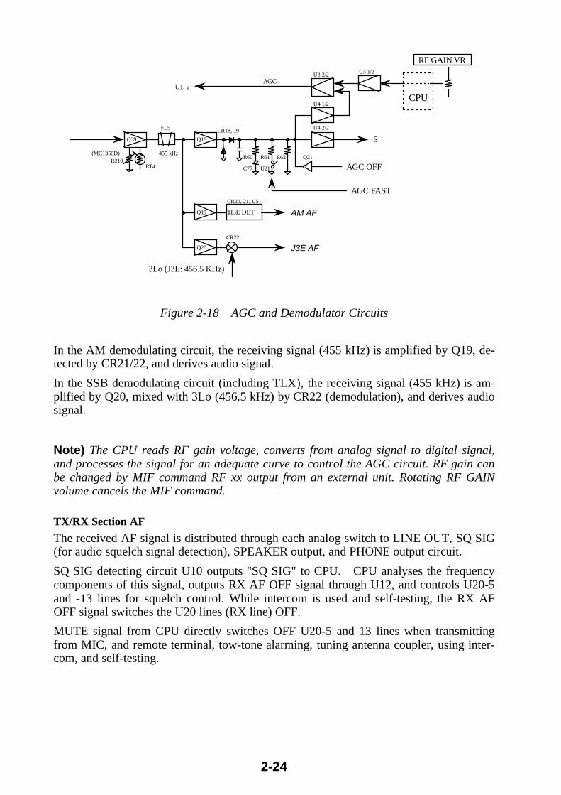
In the AGC circuit, the receiving signal (455 kHz) is amplified by Q18, and detected byCR18 and CR19. C77, R60, and R62 determine the AGC time constant.
C77 and R60 determines the AGC attack-time to be about 10 msec. R61 and R62 deter-mines AGC decay-time in AGC-FAST to be about 100 msec and R62 determines that inAGC-SLOW about 3 sec. U21 switches R61ON and OFF according to AGC-FAST andSLOW, respectively.
U4-1/2, U3-1/2, and U3-2/2 are AGC signal amplifiers. The control signal from the gainvolume* is supplied to the AGC circuit to control the gains of U1 (MC1350D) of the firstIF amplifier and U2 (MC1350D) of the second IF amplifier. The controlling method isforward AGC.
U4-2/2 amplifies the AGC voltage and detects the receiving signal strength "S". This sig-nal not only deflects S-meter, but controls the scanning, sweeping, and squelching of thereceiving signal.
In the scanning and sweeping, the AGC is automatically turned ON.
*: The voltage from the gain volume (RF GAIN VR) is read by the CPU, A/D-converted,and then processed for the volume curve. RF GAIN can also be adjusted by RFxx of MIFcommand from a remote terminal. Operation of the RF gain volume cancels the MIFcommand.
2-24
(MC1350D)R210
FL5
455 kHz
AGC
H3E DET
CR22
3Lo (J3E: 456.5 KHz)
AM AF
J3E AF
CR18, 19
Q18
Q19
Q20
CR20, 21, U5
RF GAIN VR
AGC OFF
S
RT4
U4 1/2
U4 2/2
AGC FAST
U3 2/2 U3 1/2
R60
C77
R61
U21
R62 Q21
U1, 2
Q39
CPU
Figure 2-18 AGC and Demodulator Circuits
In the AM demodulating circuit, the receiving signal (455 kHz) is amplified by Q19, de-tected by CR21/22, and derives audio signal.
In the SSB demodulating circuit (including TLX), the receiving signal (455 kHz) is am-plified by Q20, mixed with 3Lo (456.5 kHz) by CR22 (demodulation), and derives audiosignal.
Note) The CPU reads RF gain voltage, converts from analog signal to digital signal,and processes the signal for an adequate curve to control the AGC circuit. RF gain canbe changed by MIF command RF xx output from an external unit. Rotating RF GAINvolume cancels the MIF command.
TX/RX Section AF
The received AF signal is distributed through each analog switch to LINE OUT, SQ SIG(for audio squelch signal detection), SPEAKER output, and PHONE output circuit.
SQ SIG detecting circuit U10 outputs "SQ SIG" to CPU. CPU analyses the frequencycomponents of this signal, outputs RX AF OFF signal through U12, and controls U20-5and -13 lines for squelch control. While intercom is used and self-testing, the RX AFOFF signal switches the U20 lines (RX line) OFF.
MUTE signal from CPU directly switches OFF U20-5 and 13 lines when transmittingfrom MIC, and remote terminal, tow-tone alarming, tuning antenna coupler, using inter-com, and self-testing.

2-25
RX H3E
RX H3E
U183 4
5
96
8U18
SSB, TLX
AM
8
RX AF OFF
INTERCOM
113
2
96
U20
U20
U203 4
5
MUTE Q33
C139
U13 1/2
U10 1/2, 2/2
SQ SIG
LINE OUT
1 213 U19
C140
INTERCOM
C141U13 2/2
8 96 U21
SP OFF
PHONE
SP
EXT SP
AF VR
TONE
TX TONE
TX AF LINE
LINE INU20
11 10
12
U1911 10
12
LINE ON
C142
Q32
U199
68
MIC & TONE
LINE IN
U195
MIC ON
3 4U14
U15
(TDA2003H)
RX AF OFF
SP OFF
MIC&TONE
MIC ON
LINE ON
RX H3E
U11, 12
DATACLKST TX/RX
MUTECPU
MIC
(10mW/200 Ω)
Figure 2-19 RX AF Circuit

2-26
2.6 Power Supply SW Circuit
Power supply SW circuit is included in PA/FIL board.
When the power switch is turned on, a relay K1 is made ON by Q1 and power is suppliedto circuits. To protect the contact of K1 against the rush current at power on, a delay cir-cuit is provided. That is, C10 is charged through Q11 which is switched on by Q3 atpower on, and then K1 is turned on. When K1 is ON, Q11 is switched OFF, and power issupplied through K1. Turn-on of K1 is delayed until C9 is charged.
K1
Overvolt. Detector
+12 V
-12 V
+ 13.6 V
– 13.6 V
FL2
F2 (1.35 A) CR1 Q11 R2
K1
F1 (4 A)C10
R1
R4
Q3 Q2
Q1
C13 C14
C49 to 52
PA
EE
U1
POWER SW
BK + 12V
BK – 12V
JP1
JP2
TB1
TB2
TX/RX PCB
SW REG (OPTION)
J1
J3 J4
J2
12 VJ7
12 V
J1
POWER ON
+13.6 V
R12
C9
Figure 2-20 Power Supply Circuit
The allowable input voltage of power supply is from about +8 V to +17 V. (Rating volt-age: 13.6 V ± 15 %) The upper limit +17V is determined by a over-voltage detector U1and a switch Q2 and the lower limit +8 V is determined by the drive voltage of the relayK1. F1 and F2 are poly-switches. The poly-switch works as a fuse that cuts off (trip) cir-cuit with a Joule heat generated by the current flowing through it. Once the switch be-comes off, it does not recover until it cools down while power supply is off.
Note) The negative line of the power supply and the negative ground of the circuitboards (chassis) shares a common earth. When a floating ground that separates thenegative line and the negative ground is needed, an optional SW REG board is to beadded.

2-27
2.7 SW REG Board (option)
The negative line of the power supply and the negative ground of the circuit boards(chassis) shares a common earth. When a floating ground that separates the negative lineand the negative ground is needed, SW REG board is to be added.
PA/FIL board and SW REG board are connected by connectors as follows. The necessaryconnector assembly comes with to the SW REG board.
J1 J2
J2 J3
13.6 V +
13.6 V -
OPTION SW REG (05P0668)
PA/FIL (05P0667)
TB1 TB2
J7
+ 12V
30 A
30 A
J3-1 +12 V -2 +12 V -3 -0 V (GND) -4 -0 V (GND)
J1-1 +12 V -2 +12V -3 -0 V (GND) -4 -0 V (GND)
J7 -1 +12 V -2 +12 V -3 -0 V (GND) -4 -0 V (GND) -5 -0 V (GND)
PA/FIL Board SW REG Board
J2
J3
→
→
J1
J2
Figure 2-21 Connection of SW REG Board
The block diagram of the SW REG board is shown in Figure 2-22. The power supplyvoltage for the board is +13.6 V and the switching regulator outputs +13.0 mV. R15(AVR) adjusts the output voltage. The oscillating frequency of the switching regulator,measurable between TP1 and TP2, is 170 kHz ± 20 kHz, which is determined by R9 andC10 connected to U1.
RECTDRIVE FILT
CONT DET
Q1 (2SK1266) T1
U1 (µPC1094C)R15
AVRU2 (TLP521) U3 (µPC1093J)
CR1 FL1
TP2
TP1
13.6 V +
13.6 V -
+13 V-13 V
C10R9
Figure 2-22 Block Diagram of SW REG Circuit
2-28
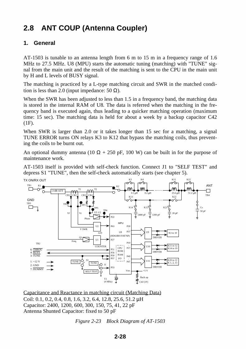
2.8 ANT COUP (Antenna Coupler)
1. General
AT-1503 is tunable to an antenna length from 6 m to 15 m in a frequency range of 1.6MHz to 27.5 MHz. U8 (MPU) starts the automatic tuning (matching) with "TUNE" sig-nal from the main unit and the result of the matching is sent to the CPU in the main unitby H and L levels of BUSY signal.
The matching is practiced by a L-type matching circuit and SWR in the matched condi-tion is less than 2.0 (input impedance: 50 Ω).
When the SWR has been adjusted to less than 1.5 in a frequency band, the matching datais stored in the internal RAM of U8. The data is referred when the matching in the fre-quency band is executed again, thus leading to a quicker matching operation (maximumtime: 15 sec). The matching data is held for about a week by a backup capacitor C42(1F).
When SWR is larger than 2.0 or it takes longer than 15 sec for a matching, a signalTUNE ERROR turns ON relays K3 to K12 that bypass the matching coils, thus prevent-ing the coils to be burnt out.
An optional dummy antenna (10 Ω + 250 pF, 100 W) can be built in for the purpose ofmaintenance work.
AT-1503 itself is provided with self-check function. Connect J1 to "SELF TEST" anddepress S1 "TUNE", then the self-check automatically starts (see chapter 5).
-3 dB ATT
U1Q1
U2
U5 1/2
CR2CR1 CR3 CR4
T1 T2
TP2 TP3TP5
A/D
COUNTER
VrVf
Freq.
Phase
V SWR
P22
TP4
P63
P27
3: TUNE4: BUSY6: THROU
J1TUNE
SELF TEST
TUNE
P51P56P50
P53
P57S1
U8
Y1 (4 MHz)
Voo
C42 (1F)
+5 V
(HD63B01Y0E76P)
K3
K2K1
K13
K4
K14 K15 K21
K22
K12K11
50 pF20 pF
2400 pF 1200 pF
0.1 µH 0.2 µH 25.6 µH 51.2 µH
U9 K3 to 10
P30 : P37
U10 K11 to 12 K14 to 19
U11 K20 to 22 K 1, 2, 13
P10 : P17
P40 : P47
ANT
TB4
TX ON/RX OUT
TB1
TB2
1: +12 V2: GND
7: DUMMY
TB3GND
DRIVER
DRIVER
DRIVER
Cs
MPU
ROM
RAM
CPU
I/O
Back up
Capacitance and Reactance in matching circuit (Matching Data)Coil: 0.1, 0.2, 0.4, 0.8, 1.6, 3.2, 6.4, 12.8, 25.6, 51.2 µHCapacitor: 2400, 1200, 600, 300, 150, 75, 41, 22 pFAntenna Shunted Capacitor: fixed to 50 pF
Figure 2-23 Block Diagram of AT-1503

2-29
2. Matching Process (TUNE/BUSY Signals)
1. When PTT switch is depressed or TX KEY is turned ON by an external device afterthe frequency change, or when TUNE switch is depressed, "TUNE" is displayed on themain unit and "TUNE" signal inputs to the antenna coupler.
2. The relays K1 and K2 are turned ON, and the detector circuits are switched ON. Thatis, RF input frequency detected by ATT, Vf/Vr (V SWR) detected by T1, and thephase detected by T2 input to U8 (MPU).
3. During matching, an about 10 W signal with a selected frequency is input to RF circuitin USB mode (Tone: 1500 Hz).
4. MPU drives the relays K3 to K22 in accordance with the data from the detector circuitand changes the constants of L/C in L-type matching circuit.
5. If SWR is less than 1.5, the matching data is stored in the internal RAM of U8. If SWRis more than 2.0 or it takes longer than 15 seconds for matching (time out), the match-ing circuit is bypassed.
6. The matching results are informed to CPU of the main unit by H and L levels of BUSYsignal.
7. RF signal is stopped, the matching results are displayed, and the condition of the mainunit is returned to that when the matching was started. If SWR is less than 2.0, TUNEOK appears, and if it is 2.0 or more, error sounds (three beeps) occur with the indica-tion TUNE ERROR.
TUNE
BUSY
TX RF
200 msec or more
40 msec
20 msec20 msec
H: TUNE OK
L: TUNE ERRORMax: 15 sec
(Tunning )See note.
(= 10 W USB)•
•
Note) If the level remains "H" for one second, TUNE ERROR is to result.
Figure 2-24 TONE Operation Timing Chart

2-30
3. Matching Circuit
AT-1503 uses two L-type matching circuits with a nominal input impedance Z of 50 Ω asshown below. Refer to Figure 2-25 for the variation of the input impedance with fre-quency.
The matching circuit in the MF band is shown below, where the antenna length is lessthan one quarter of the wavelength. The antenna impedance includes not only a resistancebut a capacitive reactance (-jXCa). In addition to matching Z to Ra, an inductance L1(loading coil) is needed to cancel an antenna capacitance Ca.
At the output side of the matching circuit, a shunt capacitor Cs is included, whichequivalently increases Ca to make it possible to match to an antenna with small Ca.
Reference) When a 6 m whip antenna is hoisted, the Ca is about 80 pF in 1.6 MHz. Inthis case LI is 120 µH that is too high. Adding Cs (50 pF) increases the equivalent valueof Ca to about 130 pF and leads to the necessary value of LI 75 µH that is within amatching range.
Z Ra
RF IN ANT equivalent circuitZ > Ra
1
ωC= Z Ra
(Z - Ra)
ωL = Z R (Z - Ra)
C
L = Lt + Ll
(50 Ω)
Lt Ll(Tank coil) (Loading coil)
Ca
RaCs
∑ = 102 µH
ANT
The matching circuit for the antenna length of longer than a quarter of the wavelength isshown below. The actual antenna has not only a resistance Ra but also a capacitance, oran inductive reactance in an antenna length range. In addition to matching Z to Ra, acoupling capacitor Cc is needed to cancel the antenna reactance
Z Ra
RF INZ < Ra
1
ωC= Z
(Ra - Z)
ωL = Z (Ra - Z)
Ct
L
(50 Ω)
Antenna equivalent circui
Ca
Ra Ra
LaCs
(Tank coil)
Cc
C = Ct + Cc
(Coupling C) (Annten C)
∑ = 4788 pF
ANT
Inductive
Capacitive
Antenna Length
λ/4 λ/2
Reactance
Ra: Resistance30 to 40 Ω
(+jXL)
(-jXC)
3λ/4
Figure 2-25 Change of Antenna Impedance

2-31
Matching Flow Chart
Start
Detector ON
Vf Read
SWR Calculation
Freq. Read
Matching operation
Detector OFF
Sleep mode
SWR Calculation
Keeping relays off
Outputting TUNE END
Bypass
Keeping relays on
Outputting TUNE END and TUNE ERROR
Vf > Data obtained
SWR < 1.5
SWR < 1.5DATA Retrieve
RAM DATA in us ?
YES
YES
YES
NO
NO
NO
K1, K2 (Freq./VSWR/Phase detection)
Checking RF Input
Checking RF Input Frequency
"H" BUSY
See next page.
K3 to K12 ON
"L" BUSY
YES
NO
Figure 2-26 Matching Flow Chart
2-32
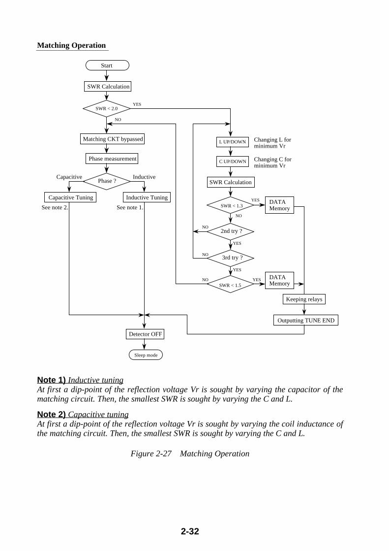
Matching Operation
Start
Phase measurement
Sleep mode
Outputting TUNE END
Matching CKT bypassed
Capacitive Tuning
Phase ?
SWR < 1.3
Capacitive
YES
Inductive
NO
SWR Calculation
SWR < 2.0
Inductive Tuning
L UP/DOWN
C UP/DOWN
SWR Calculation
SWR < 1.5
DATA Memory
2nd try ?
3rd try ?
YES
YES
YES
NO
NO
Keeping relays
Detector OFF
See note 1.See note 2.
Changing L for minimum Vr
Changing C for minimum Vr
NO
NO
YES
DATA Memory
Note 1) Inductive tuningAt first a dip-point of the reflection voltage Vr is sought by varying the capacitor of thematching circuit. Then, the smallest SWR is sought by varying the C and L.
Note 2) Capacitive tuningAt first a dip-point of the reflection voltage Vr is sought by varying the coil inductance ofthe matching circuit. Then, the smallest SWR is sought by varying the C and L.
Figure 2-27 Matching Operation
2-33
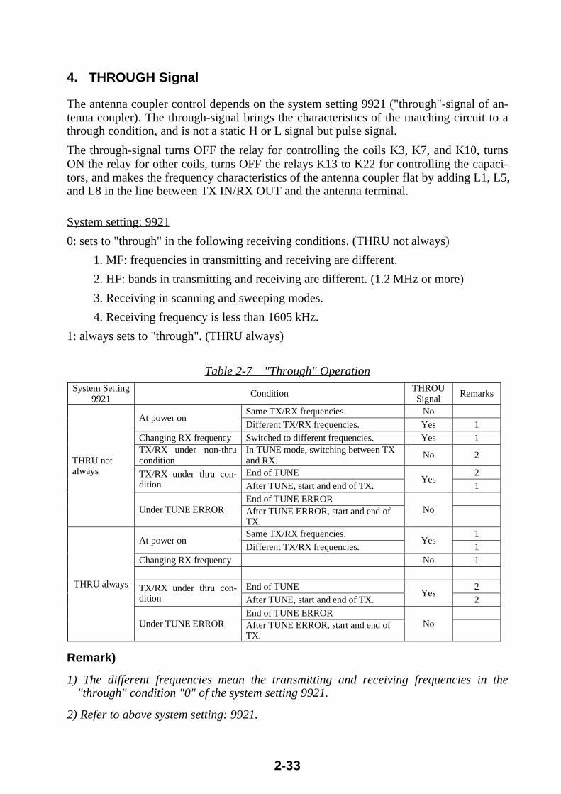
4. THROUGH Signal
The antenna coupler control depends on the system setting 9921 ("through"-signal of an-tenna coupler). The through-signal brings the characteristics of the matching circuit to athrough condition, and is not a static H or L signal but pulse signal.
The through-signal turns OFF the relay for controlling the coils K3, K7, and K10, turnsON the relay for other coils, turns OFF the relays K13 to K22 for controlling the capaci-tors, and makes the frequency characteristics of the antenna coupler flat by adding L1, L5,and L8 in the line between TX IN/RX OUT and the antenna terminal.
System setting: 9921
0: sets to "through" in the following receiving conditions. (THRU not always)
1. MF: frequencies in transmitting and receiving are different.
2. HF: bands in transmitting and receiving are different. (1.2 MHz or more)
3. Receiving in scanning and sweeping modes.
4. Receiving frequency is less than 1605 kHz.
1: always sets to "through". (THRU always)
Table 2-7 "Through" OperationSystem Setting
9921Condition THROU
SignalRemarks
Same TX/RX frequencies. NoAt power on
Different TX/RX frequencies. Yes 1Changing RX frequency Switched to different frequencies. Yes 1TX/RX under non-thrucondition
In TUNE mode, switching between TXand RX.
No 2
End of TUNE 2TX/RX under thru con-dition After TUNE, start and end of TX.
Yes1
End of TUNE ERROR
THRU notalways
Under TUNE ERROR After TUNE ERROR, start and end ofTX.
No
Same TX/RX frequencies. 1At power on
Different TX/RX frequencies.Yes
1Changing RX frequency No 1
End of TUNE 2TX/RX under thru con-dition After TUNE, start and end of TX.
Yes2
End of TUNE ERROR
THRU always
Under TUNE ERROR After TUNE ERROR, start and end ofTX.
No
Remark)
1) The different frequencies mean the transmitting and receiving frequencies in the"through" condition "0" of the system setting 9921.
2) Refer to above system setting: 9921.

2-34
2.9 Interface
1. REMOTE (A), (B)
An optional REMOTE board is needed to connect DSC, NBDP terminal, remote station(RB-500), and distributor (DB-500, DB-120).
One of two types of REMOTE boards is selected according to the connecting device, (A):05P0457 for RS-232C and (B): 05P0458 for current loop.
⋅ Devices with RS-232-C: DSC-5/6, DP-5/6, DB-120, DB-500
⋅ Devices with current loop: RB-500, DB-500
Note) DB-500 is applicable to both types with modifications in the REMOTEboards.
Level Converter (IC)
U4 (MC145406AP)
LINE IN
LINE OUT
RX MUTE
TX KEY
TXD
RXD
U5 (PC357NT)
U5 (PC357NT)
TX/RX AF Circuit
CPU Board
REMOTE (A) (05P0457)
DSC/NBDP
REMOTE 1- TD-H 2- TD-C 3- RD-H 4- RD-C 5- F.GND 6- +12 V 7- +12 V 8- S GND 9- S GND 10- LINE OUT H 11- LINE OUT C 12- LINE IN H 13- LINE IN C 14- TX KEY 15- RX MUTE 16- NC
0 dBm
RS-232C
REMOTE (B) (05P0458)
Level Converter
TXD
RXDU2 (PC357NT)
Q1 (2SA1586)
Note) REMOTE Boards A and B have a different level converter.
Current Loop
REMOTE
RX MUTE
TX KEY
Figure 2-28 Remote Terminal Connection

2-35
Operation with MIF Command
The FS-1503 can be controlled by MIF commands from Furuno's NBDP, DSC and re-mote station.
The following explains how MIF command from the DP-6 controls the FS-1503.
Operation on DP-6
1. Press [F4] (window).2. Select "3: Remote A (TX/RX).
Window 1: Display NMEA Data 2: Calendar 3: Remote A (Tx/Rx) 4: Remote B (DSC) 5: Distress Frequency Tabile
3. Enter a command and a parameter. For example, type FT1234560 and press [Enter] toset TX freq. to 12345.60 KHz.
4. If the entered command is executed, * appears. If not, ? appears.
Remote MIF > FT1234560 MIF > *
Radiotelephone DP-6
Start
Command Output
Output next command
Executing
Response signalOutput
Correct command ?
* received ?
YES
NOYES
NO
Response Signal
⋅ *CR (LF) --- When a command is executed correctly.
⋅ ?CR (LF) --- When a command is incorrect or an error occurs during theexecution.

2-36
MIF Command List
Command Description
DRS Keylock setting, getting highest priority. (DISTRESS)
DRR Releasing keylock, (DISTRESS)
FZS Keylock setting, Highest priority to 2182 KHz from main unit (FREEZE)
FZR Releasing keylock, (FREEZE)
EM* [*; 0: LSB, 1: J3E, 2: H3E, 5: TLX, 6: FAX]
FT******* TX freq. setting, *: 1234560 for 12,345.60 KHz, for example
FR******* RX freq. setting, *: 1234560 for 12,345.60 KHz, for example
ST**** Registeration of class of emission and TX/RX frequency onto user channel
CH**** User channel setting, *: band + channel
RC**** User channel setting (Recall)
CHI***** ITU Channel setting
RCI***** ITU channel setting (Recall)
AGS AGC on setting
AGR AGC off setting
RF** RF Gain setting, [*; FF: RF GAIN MAX to 00: RF GAIN MIN]
SQS Squelch on setting
SQR Squelch off setting
SCS start scanning
SCR stop scanning
PO* TX power setting, [*; 0, 1, 2: LOW, 3: HIGH]
TU TUNE OK; [*], TUNE ERROR; [?] Tuning,
IC*S Intercom calling, *: Call number
IC*R Intercom call termination, *: Call number
CAID Confirmation of model name, [#IDFS1503] responded
CAEM Confirmation of class of emission, [#EM*] responded
CAFT Confirmation of TX frequency, [#FT*******]
CAFR Confirmation of RX frequency, [#FR*******]
CACH Confirmation of channel setting, [#CH****], [#CHI*****] responded
CARC Confirmation of, [#RC****], [#RCI*****] responded
CAAG Confirmation of AGC setting, [#AGS (AGC ON)], [#AGR (AGC OFF)] responded
CARF Confirmation of RF gain setting, [#RF**] responded,*; 00 to FF
CASL Confirmation of S level, [#SL**] responded,*; 00 to FF
CASQ Confirmation of squelch setting, [#SQS (SQ ON), #SQR (SQ OFF)] responded
CAPO Confirmation of TX power, [#PO*] responded

2-37
2. CONTROLProviding a BK line requires an optional CONTROL board. Current capacity ofCR1,Vobc) in the BK line is 1A.
U3 (PC357NT)
RX MUTE
CONTROL (05P0459)
CPU Board
Receiver
CONTROL 1- GND 2- NC 3- TX KEYED 4- RX MUTE 5- BK 12V (+) 6- BK 12V (-) 7- NC
BK +12 V/24 V
CR1Q3
(2SD799)
(V06C)
TX KEYED
+5 V
U5 (PC357NT)
RX MUTE
TX KEYED
L1
L2
CR2 (V06C) BK 12 V +
BK 12 V -
JP1
JP2
12 V +
12 V -
BK RL
BK +
CONTROL
orQ2
TX KEYED/
RX MUTE
Figure 2-29 CONTROL Board

3-1
3.1 Main Unit
1. FS-1503 Front Panel
Internal Speaker
MIC/HANDSET FREQ/CH
RF GAINPower SW & AF GAIN
LCD
2. FS-1503 Rear Panel
13.6 VDC
SPKRREMOTE(OPTION)
CONTROL(OPTION)COUPLER
ANT
GND
Chapter 3 Location of Parts

3-2
3. TX/RX Board
Q25: 2SC3133FL-3: 0.4 kHz[Option]
C554(Freq. ADJ)
30 A × 2
13.6 V
VCODDS
FAN
Y501REF X’ tal: 36 MHz
R101(H3E CARR)
R156(TX GAIN)
CONTROL05P0459
(OPTION)
A: 05P0457 (RS-232C)B: 05P0458 (Current Loop)
REMOTE(OPTION)
R210(RX GAIN)

3-3
4. PA/FIL Board (05P0667)/SW REG Board (05P0668)
TX FIL Circuit
B1 B4 B2 B5 B3 B6 (Note 1)
R39(PA BIAS)DRIVE: 2SC3133 PA: 2SC3240
R15 (13 V ADJ)
J9 BC BAND FIL (Note 2)
J8
SW REG05P0668
(OPTION)
Note 2) BC BAND FIL Setting• J9, 8 : 1.6 to 30.0 MHz• J8, 9 : 0.1 to 30.0 MHz (Default)
Note 1) TX FIL ranges• B1: 0.1 to 2.4• B2: 2.4 to 3.6• B3: 3.6 to 6.0• B4: 6.0 to 10.0• B5: 10.0 to 18.0• B6: 18.0 to 30.0 MHz
1
2

3-4
5. CPU Board (05P0665)
SP: 8 Ω/0.3 W
U5: X24C16S(EEROM)
CR1(CPU RUN)
U2: HD61602(LCD CONT)
U6: HD6475328(CPU)
R1(LCD Bril. Adj.)

3-5
3.2 AT-1503
1. AT-1503 (05P0669)
(Standard type)
S1 (TUNE)
TB 2
GND
F1: 1.35 A(Switch)
TX IN/RX OUT
ANT
R2 (BAL ADJ or ADJ)
U8: HD63B01Y0E76P(CPU)
J1(SELF TEST/TUNE)
(Built-in dummy type: optional)
DUMMY: 05P0670(OPTION)

3-6
3.3 Power Supply Unit
1. PR-200
635S1002
Front
Right-hand Side View
FAN
Front
Top View
635S1001
Front
R6 (13.6 V AVR ADJ)
R24(32 V: Short-circuit)
Left-hand Side View

3-7
2. PR-270
Front
Right-hand Side View
Front
Change tap connectionaccording to ship’s mains.(0, 110, 120 V)
R5(13.6 V AVR ADJ)
635S1001
635S1002
Top View
Front
Left-hand Side View

4-1
The system channels list is shown on the next page. The system channels marked * canonly be set by a Furuno service agent or dealer. These channels can be recalled by enter-ing the password. The procedure for changing user settable system settings appears in theOperator's Manual.
The figure below shows the setting-up procedure of the FS-1503.
System Channel 9998 Setting(Select 0 or 1)
Changing System Settings
Power ON
Registering User - Channel
0-01 to 99channel1-00 to 99channel
TX/RX Frequencies
Adjusting TX Power
High - Power ([ENT] + [8])
Low - Power([ENT] + [9])
Tune - Power([ENT] + [7])
Channel Name(7 Letters)
[CH] + Power ON
CH9999→ [CH], Password [ENT]CH99xx → [CH], Changing Setting, [ENT]
0: TX/RX Freg. Setting and Power Adj.1: TX/RX Freg. Setting
Resetting System Channel 9998
Power OFF
Power OFF→ ON
Power OFF→ [CH] + Power ON
0 - 01 to 65
Chapter 4 System Settings

4-2
4.1 Changing System Settings
1. While pressing and holding down [CH], turn the power on. System channel 9942,setting number 1, and MEMO appear on the screen.
9 9 4 2
1
MEMO
System channel
Preset value
2. Select the system channel 9999 by rotating the FREQ/CH knob.
3. Enter a password. (Press [CH], type password, and then press [ENT].)
4. Select a channel to be changed its setting by rotating the FREQ/CH knob.
5. Change the setting. (Press [CH], enter setting number, and then press [ENT].)
6. To change another channel, repeat steps 4 and 5.
7. Turn the power off and on again to store the settings.

4-3
4.2 System Channels List
Note that channels marked by * can be recalled by entering the password on systemchannel 9999.
Setting DefaultCHNo. Function
0 1 2 3 4 Std USA Thai.
9900 * Country Standard USA Thai. 0 1 2
9901 * User Channel Clear [CH] [1] [ENT]
9902 * TX PWR Data Clear [CH] [1] [ENT] 150 W 150 W 100 W
9903 * TX Frequency Free ITU/ROM ROM Marine
Free 1 1 2
9904 * RX Frequency Free ITU/ROM ROM Marine
Free 0 0 2
9905 * ITU Channel Standard USA Standard +MF 0 1 0
9906 * CH/Freq. Indication CH/Freq. Freq. CH 0 0 0
9908 * TLX (Telex) Usage TX/RX RX Disable 2 2 2
9909 * TLX RX Bandwidth Wide(2.4 k)
Narrow(0.4 k) 0 0 0
9910 * System Delay 5 to 50 ms 10 10 10
9911 * H3E (AM) Usage TX/RX RX Disable 2182 1 + 3 4 4 3
9912 * 2182 kHz Class ofEmission H3E J3E H3E
Fixed 0 0 0
9914 * LSB Usage TX/RX RX Disable 2 2 2
9915 * FAX (WeatherFacsimile) Usage TX/RX RX Disable 1 1 2
9917 * 2-tone TX, Test TX
2-tone:EnableTest:
Disable
BothEnable
BothDisable 0 0 0
9918 * Test Alarm TXFrequency 1605.00 to 29999.9 kHz 2191 kHz
9919 * Squelch during RXof 2-tone Not Open Open 1 1 1
9920 * TX TUNE Enable Disable Auto 0 0 0
9921 * THRU Signal Limited RX 0 0 0
9922 * Meter Indication IA RF 1 1 1
9924 * Remote SignalFormat MIF TBUS 0 0 0
9942 Key Response Tone OFF ON 1 1 1
9943 Noise Blanker OFF ON 1 1 1
9951 Scan Stop SignalLevel SQ Level S: 1 to 10 3 3 3
9952 Scan Dwell Time RX 1 to 99 sec 2 2 2
9953 Sweep Width 0.01 to 30000.00 kHz 100.0 kHz
9954 Sweep StepFrequency 0.01 to 30000.00 kHz 1.00 kHz
9955 Squelch Activation Freq. Level AND OR 3 3 3
9956 Squelch Level S: 0 to 10 5 5 5
9957 Squelch Decay Time 500 to 4000 msec 1000 msec
9958 Squelch ActivatingFrequency 500 to 2000 Hz 1000 Hz
9998 * User ChannelMemory/Power Adj. Enable TX/RX RX Disable 2 2 3
9999 Password [CH] (Password) [ENT] to access asterisk-marked channels.

4-4
Description of System Channel
1. 9900 (Country)System settings 9903 and above are preset to default values depending on local rulesand regulations.
2. 9902 (TX power data clear)Power data is changed to default settings as below.⋅ Standard, USA HIGH: 220 (150 W) LOW: 140 TUNE: 40⋅ Thai HIGH: 170 (100 W) LOW: 140 TUNE: 40
3. 9903 (TX frequency)⋅ 0: Free: Frequencies can be selected in the range of 1.6065 MHz to 29.9999
MHz. ITU and User channels are also available.⋅ 1: ITU/ROM: ITU and User channels are available.⋅ 2: ROM: User channel only⋅ 3: Marine Free: Frequencies can be selected in the following range. ITU and User
channels are also available.1606.5 – 4438; 6200 – 6525; 8100 – 8815; 12230 – 13200;16360 – 17410; 18780 – 19800; 22000 – 22855; 25070 – 26175 kHz
4. 9904 (RX frequency)
⋅ 0: Free: Frequencies can be selected in the range of 0.1000 MHz to 29.9999MHz. ITU and User channels are also available.
⋅ 1: ITU/ROM: ITU and User channels are available.⋅ 2: ROM: User channel only⋅ 3: Marine Free: Frequencies can be selected in the following range. ITU and User
channels are also available.1606.5 – 4438; 6200 – 6525; 8100 – 8815; 12230 – 13200;16360 – 17410; 18780 – 19800; 22000 – 22855; 25070 – 26175 kHz
5. 9905 (ITU channel)Refer to appendix 2 for ITU channel list.

4-5
6. 9906 (Channel/Frequency Indication)⋅ 0: CH/Freq: The selected RX channel and frequency are displayed on the up-
per and lower rows respectively. The selected TX channel andfrequency are indicated when the PTT switch is depressed.Both TX and RX frequency can be momentarily displayed on theupper and lower rows respectively by pressing [ENT].While pressing and holding down [ENT], press [CUSR] formomentary call of channel name or station name.
⋅ 1: FREQ: TX and RX frequencies are indicated on upper and lower rowsrespectively. The channel number are displayed momentarilywhen [ENT] is pressed.
⋅ 2: CH: TX and RX channels are indicated on upper and lower rows re-spectively. However, if a channel is preset by a frequency, in-stead of channel number, the frequency is displayed.Pressing [ENT] changes the display from “channel” to “fre-quency” momentarily.
7. 9909 (TLX RX Bandwidth)⋅ 1: Narrow (0.4 kHz) requires an optional filter, SF0L04.
8. 9910 (TLX System Delay)Set to “10 msec” normally.
9. 9912 (2182 kHz Class of Emission)Selects class of emission for 2182 kHz signal when [2182] is pressed.[MODE] is inoperative if 2:H3E fix is selected.
10. 9917 (2-tone TX, Test TX)⋅ 0: Pressing [2182], and then [ALM] and [ENT] together emits 2-tone alarm signal for 45 seconds. 9912 must be set to 0 or 2. The alarm TX frequency is selected
on 9918.⋅ 1: In addition to 2-tone alarm TX, test transmission is available if an optional dummy load 05P0670 is fitted. Press [ALM] and [INT] together, and test signal on the frequency selected on 9918 is transmitted for 45 seconds into the
dummy. 11. 9919 (Squelch during 2-tone alarm reception)
⋅ 0: (Not open): 2182 kHz squelch frequency is set on 9958.⋅ 1: (Open): 1300 Hz signal of 2-tone alarm opens squelch.
12. 9920 (TX TUNE)⋅ 0: (Enable): Tuning is made when the PTT switch or [TX TUNE] is de-
pressed.⋅ 1: (Disable): No tuning function⋅ 2: (Auto): Tuning is made when the TX frequency is changed.

4-6
13. 9921 (THRU signal)⋅ 0: Limited: RX signal does not pass through tuning circuit:
1) When TX and RX frequencies on MF are different.2) When TX and RX band on HF are different.(frequency sepa-ration of more than 1.2 MHz)3) At scan/sweep reception
⋅ 1: RX: RX signal does not passe through tuning circuit during reception.
14. 9922 (Meter Indication)⋅ 0: IA: The meter indicates antenna current (IA).
(The IA cannot be selected on the standard type.)⋅ 1: RF: The meter indicates RF output level.
15. 9924 (Remote Signal Format)⋅ 0: MIF: Furuno radio interface. Selected when Furuno DSC or NBDP
terminal is connected.⋅ 1: TBUS: For equipment made by "Thrane & Thrane A/S" of Denmark.
16. 9951 (Scan Stop Signal Level)⋅ 0: SQ Level: Scan stops when the squelch opens.⋅ 1 to 9: Scan stops when receiving signal level is higher than the preset
level.
17. 9955 (Squelch Activation)⋅ 0: Freq.: The squelch opens when the receiving signal is lower than the
preset value (9958).⋅ 1: Level: The squelch opens when the S-meter is higher than the preset
value (9956).⋅ 2: AND: The squelch opens when both frequency and level are satisfied.⋅ 3: OR: The squelch opens when either frequency or level is satisfied.
18. 9958 (Squelch Activating Frequency)If a detected signal is lower than the preset one, it is recognized as audio signal, ifhigher, it is noise.

4-7
19. 9998 (User Channel Memory/Power Adjustment)⋅ 0: Enable: Enabling to write TX and RX frequencies and adjust TX power
on user channels.⋅ 1: TX/RX: Enabling to write TX and RX frequencies on user channels.⋅ 2: RX: Enabling to write RX frequencies on user channel.⋅ 3: Disable: Disabling to write frequencies and adjust TX power on user
channel.
20. 9999 (Password)While pressing and holding down [CH], turn on the unit. Press [CH], enter apassword, and then press [ENT]. All system settings can be changed.

4-8
4.3 Channel Programming
199 user channels are divided into two bands; 0 and 1. Further channels are divided intoten scan groups which are able to be scanned as a group.TX and RX frequencies and class of emission can be preset on each user channel.
In addition, a user channel name can be entered on 65 channels, 0-01 to 0-065.
Band Channel ScanGroup
Remarks Band Channel ScanGroup
Remarks
01 to 09 00 to 09
10 to 19 10 to 19
20 to 29 20 to 29
30 to 39 30 to 39
40 to 49 40 to 49
50 to 59 50 to 59
60 to 69 60 to 69
70 to 79 70 to 79
80 to 89 80 to 89
0 1 to 99
90 to 99
1 0 to 99
90 to 99
How to program user channel
1. While pressing and holding down [CH], turn the power on.
2. Select system channel 9999 by rotating the FREQ/CH knob.
3. Enter a password. (Press [CH], type password, and then press [ENT].)
4. Select channel 9998 by rotating the FREQ/CH knob.
5. Press [CH], [1], and [ENT] in this order to enable channel programming.If [CH], [0], and [ENT] are pressed, not only channel programming but also poweradjustment can be made.
6. Select an RX channel to be programmed by rotating the FREQ/CH knob. The displaychanges as follows when the knob is rotated: RX frequency, TX frequency, and chan-nel name can be preset on a channel in this order. Note that the channel name cannotbe entered on channel 66 and above.[0-01⋅R] → [0-01⋅T] → [0-01⋅-----] → [0-02⋅R] → [0-02⋅T] → [0-02⋅-----] →⋅⋅⋅⋅⋅⋅⋅⋅⋅⋅⋅⋅⋅⋅⋅⋅⋅⋅⋅⋅[1-00⋅R] → [1-00⋅T] → [1-01⋅R] → ----------
7. Select the emission mode by pressing [MODE]: J3E for SSB radiotelephone and TLXfor DSC and NBDP.

4-9
8. Enter a receiving frequency(R): Press [CH], enter a frequency with numeric keys, andthen press [ENT]. Reenter a frequency after pressing [CH] if necessary.
9. Rotate the FREQ/CH knob cw by one click to select the TX frequency(T) on thesame channel.
10. Enter a transmitting frequency: Press [CH], enter a frequency with numeric keys, andthen press [ENT]. If the transmitting frequency is the same as the receiving frequency,press [ENT] without typing the frequency.
If you do not need to register a channel name, skip steps 11 through 14.
How to register channel name
11. Rotate the FREQ/CH knob cw by one click, the following display will appear.
0-01
- - - - - - -
MEMO
Channel Number
Channel Name
12. Press [CH], and select a desired number or alphabet by rotating the FREQ/CH knob.And then press [ENT].
13. Rotate the FREQ/CH knob to select a desired alphanumeric for the next character,and press [ENT].
14. Do the same to complete a channel name (max.7 characters). After entering the lastcharacter, cursor disappears automatically and the channel name is registered.
15. Rotae the FREQ/CH knob cw by one click to register the RX frequency on anotherchannel. Or, set the system channel 9998 to the default value (2 or 3) to terminate thesetting.
16. Turn off the power to store programmed channels.
The following pages describes how to delete a frequency and how to erase/change achannel name.Now that system channel 9906 must be set to “0” for displaying a channel name.

4-10
How to erase programmed frequency
1. Follow steps 1 to 5 described in “How to program user channel” on page 4-8.
2. Select an RX channel to be erased by rotating the FREQ/CH knob.(For example, 0-010R)
3. Press [CH], [0], and [ENT] in this order.
4. Rotate the FREQ/CH knob cw by one click to select the TX channel.(For example, 0-01T)
5. Press [CH], [0], and [ENT] in this order.
To erase another user channel, repeat steps 2 to 5. All user channels can be erased at atime: On system channel 9901 press [CH], [1], and [ENT] in this order.
How to erase channel name
1. Select a channel name to be erased. (Carry out steps 1 to 5 on page 4-8, and select thechannel name by rotating [FREQ/CH] knob.)
2. Press [CH], [0], and [ENT] in this order.
How to change channel name
1. Select a channel name to be changed. (Carry out steps 1 to 5 on page 4-8, and selectthe channel name by rotating [FREQ/CH] knob.)
2. Press [CH], and then press [ENT] several times until the cursor moves onto thecharacter to be changed.
3. Rotate [FREQ/CH] knob to select a new character, and press [ENT].
4. Repeat steps 2 to 3.
5. Move the cursor onto the 7th character and press [ENT].

4-11
Symbols for Channel Name
The radiotelephone employs symbols to indicate channel names. The symbols and theircorresponding letter are shown below.
A B C D E F G H I
J K L M N O P Q R
S T U V X Y Z
0 1 2 3 4 5 6 7 8
9 –
W
Note) To indicate the channel name, system channel 9906 must be set to “0:CH/FRQ”.The channel name appears every time [CURS] is pressed while pressing andholding down [ENT].

4-12
4.4 Power Data Setting
The output power can be set by changing power data through the keyboard. Adjustmentof any potentiometers inside the unit is not necessary. Frequency ranges in which powerdata is effective are tabled on the next page.
System channel 9998 must be set to “0” for power adjustment. After the adjust-ment, system channel is set back to the previous value.
HI (normal) power
⋅ Power data for each user channel and 2182 kHz is set individually.
⋅ Where manually entered frequency or ITU channel is permitted, the data is set on eachband and each class of emission.
⋅ J3E power data is also used for LSB power data.
LOW (reduced) power
⋅ Power data for 1.6 to 3.9999 MHz is set in each class of emission.
⋅ Where manually entered frequency or ITU channel is permitted, the data is set on eachband and each class of emission.
⋅ J3E power data is also used for LSB power data.
TUNE power (Factory-adjusted)
⋅ Normally the TUNE power adjustment is not necessary. Power data set on a channel isused on all channels.

4-13
Frequency Ranges for Power Adjustment
Power data can be set on following frequency ranges and classes of emission,(Marked by “•”). Power data for user channel is entered for all classes of emission.
HI Power LOW Power
J3E H3E TLX J3E H3E TLX
BAND
1.6 - 1.9999 • • •
2.0 - 2.4999 • • •
2.5 - 2.9999 • • •
3.0 - 3.4999 • • •
3.5 - 3.9999 • • •
• • •
4.0 - 5.9999 • • • • • •
6.0 - 7.9999 • • • • • •
8.0 - 11.9999 • • • • • •
12.0 - 15.9999 • • • • • •
16.0 - 17.9999 • • • • • •
18.0 - 21.9999 • • • • • •
22.0 - 24.9999 • • • • • •
25.0 - 29.9999 • • • • • •
ITU Channel
Using above data for each frequency range and in each emission modes.
User Channel
0 - 01 to 99
1 - 00 to 99Power data is set on each channel.
Using above data for each frequencyrange and in each mode.
[2182] key
• Power data entered for 1.6 - 3.9999MHz.
Default setting of power data
⋅ Standard and USA (150 W): 220
⋅ Thai (100 W): 170
⋅ LOW (60 to 70 W): 140
⋅ TUNE (10 W): 40

4-14
How to adjust HI power
1. Select a TX channel. For example, select the ITU channel 401.
2. Press [TUNE/7].TUNE appears on the display and the coupler starts tuning. When the tuning iscompleted successfully, TUNE OK appears.
3. While pressing and holding down [ENT], press [8], and HI power data appears.
4001
220
J3E
ITU Channel Number
HI Power DataITU R
AGC
DUP
T appears during TX.
0 2 4 6 8 10
During TX, RF output level can be read.
NB
TR
4. Set power data by rotating the FREQ/CH knob.The data can be set to from low power data plus 1 to 255. Read the power meter, ifconnected, while pressing the PTT switch and whistling or speaking into the handset.
5. Press [ENT] to register the power data.
6. Repeat steps 1 to 5 to set another power data.
Power Data vs. Output Power (50 ohm dummy load connected)
Power Data 255 240 220 200 180 160 140 120 100 80 60 40 20 10 0Output(Wpep) 160 158 150 130 110 90 72 58 45 34 24 16 8 5 3
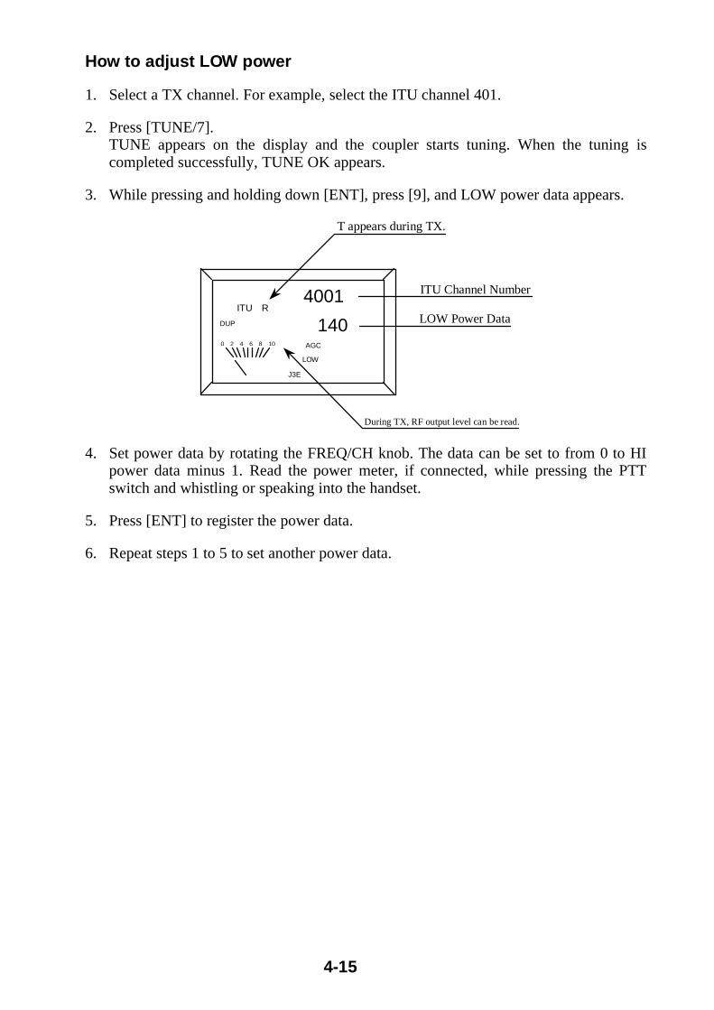
4-15
How to adjust LOW power
1. Select a TX channel. For example, select the ITU channel 401.
2. Press [TUNE/7].TUNE appears on the display and the coupler starts tuning. When the tuning iscompleted successfully, TUNE OK appears.
3. While pressing and holding down [ENT], press [9], and LOW power data appears.
4001
140
J3E
ITU Channel Number
LOW Power DataITU R
AGC
DUP
T appears during TX.
0 2 4 6 8 10
During TX, RF output level can be read.
LOW
4. Set power data by rotating the FREQ/CH knob. The data can be set to from 0 to HIpower data minus 1. Read the power meter, if connected, while pressing the PTTswitch and whistling or speaking into the handset.
5. Press [ENT] to register the power data.
6. Repeat steps 1 to 5 to set another power data.
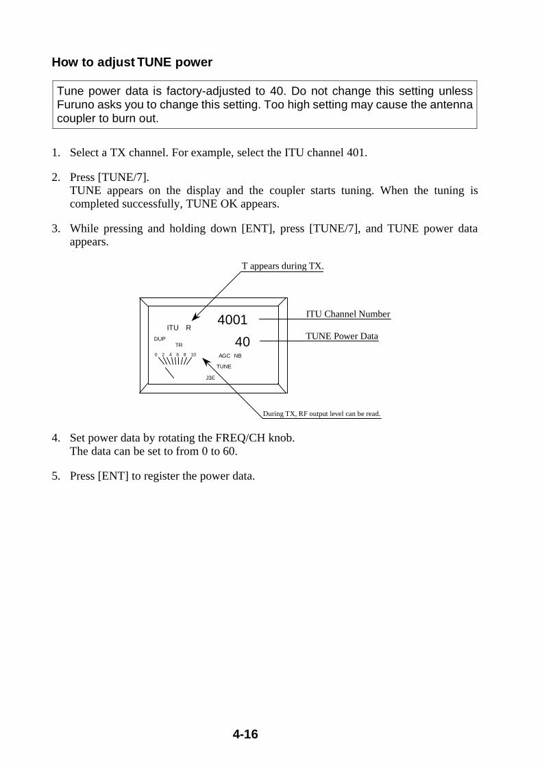
4-16
How to adjust TUNE power
Tune power data is factory-adjusted to 40. Do not change this setting unlessFuruno asks you to change this setting. Too high setting may cause the antennacoupler to burn out.
1. Select a TX channel. For example, select the ITU channel 401.
2. Press [TUNE/7].TUNE appears on the display and the coupler starts tuning. When the tuning iscompleted successfully, TUNE OK appears.
3. While pressing and holding down [ENT], press [TUNE/7], and TUNE power dataappears.
4001
40
J3E
ITU Channel Number
TUNE Power DataITU R
AGC
DUP
T appears during TX.
0 2 4 6 8 10
During TX, RF output level can be read.
TUNE
NB
TR
4. Set power data by rotating the FREQ/CH knob.The data can be set to from 0 to 60.
5. Press [ENT] to register the power data.

4-17
4.5 BC Band Filter Setting
If MF/HF band is interfered with broadcast(BC) band, change jumper settings J8 and J9from "2" to "1."
Position "1": Receiving frequency range from 1.6 MHz to 30 MHz
Position "2": Receiving frequency range from 0.1 MHz to 30 MHz
PA / FIL Board
J8J9
0.1 to 30 MHz
1.6 to 30 MHz
SW REG Board (OPTION)
2
1
2
1Factory-Setting [ ]2BC BAND FIL
2
1
1.6 MHz HPF (High Pass Filter) is added on the receiving line with jumpers 8 and 9 setto "2".

4-18
4.6 Setting for NBDP (DP-6)
When the NBDP DP-6 is connected to the radiotelephone, the following setting must becarried out.
Setting on DP-6
1. On the DP-6, press [F6], and enter the password for system setting. The setting mustbe as below.
System
Set up Lock Change Default
Slave Delay 5 msec (0 - 50msec)BK Timing Pre Tone 10 msec (0 - 100msec) Post Tone 0 msec (0 - 20msec)Mute Timing Pre BK 0 msec (0 - 20msec) Post BK 0 msec (0 - 20msec)
Mdem Output Level 0 dBm (-30 - +10 dBm)
MIF Tune OFF ONFreeze OFF ONAGC OFF ONEmission OFF ON
TX/RX MSG Save OFF ONEdit Before Sending OFF ON
Timer System OFF UTC STM JSTTime & DateDisplay Mode Normal ReverseSelf Test
**********
• Slave Delay 5 msec• BK Timing Pre Tone 10 msec• Post Tone 0 msec• Mute Timing Pre BK 0 msec• Post BK 0 msec• Modem Output Lervel 0 dBm• MIF Tune ON• Freeze ON or OFF• AGC ON• Emission ON
[F6] System Setup Menu
2. Press [F5] and enter the answerback code and the ID.
Setting on FS-1503
⋅ 9908 (TLX usage): 0 (TX/RX)
⋅ 9909 (TLX RX bandwidth): 1 (Narrow) -------- Optional 0.4 kHz filter required
⋅ 9910 (System delay): 10 msec
⋅ 9921 (THRU signal to couper): 0 (Limited)
⋅ 9924 (Remote signal format): 0 (MIF)

5-1
Electrical Shock Hazard:This equipment contains high voltages which can cause death at several internal circuits. Any internal adjustment, servicing and repair shall only be perfomed by qualified service personnel totally familiar with electrical circuits and servicing of the equipment. A residual charge remains in capacitors and other devices several minutes after turning off the power.It is therefore essential to wait at least 3 minutes to allow residual charge to subside before acceessing the inside of the equipment.
DANGER
5.1 Periodical Checks
Regular maintenance is important for good performance. Before performing any mainte-nance, turn off the power.
1) Cleaning of the display
Use a soft cloth with a slight amount of anti-static-charge spray. Do not use thinner andbenzene for cleaning.
2) Connections
Check connections on the main unit and the antenna coupler for loose connections. Poorgrounding on the antenna coupler decreases the output power from the antenna. The con-nectors inside the unit are also checked at least every half year.
3) Insulators
Check for damage and salt deposits. Remove salt deposits with fresh water. Replacedamaged insulators.
4) Water leakage
Check the antenna coupler for water leakage.
Chapter 5 Maintenance

5-2
5.2 Self-test
Both the main unit and the antenna coupler contain a self-test facility which can checkthem for proper operation. The test checks transceiver circuit, LCD, keyboard, and an-tenna coupler.
Note) If the dummy board is not fitted, the test is carried out only for TX/RX board.
Transceiver Check
1. While pressing and holding down [TX] key, turn on the power.
2. Release the hand from [TX] when all indications appear on the screen. The test com-mences and the display changes as follows.
R Good
T GoodE
T GoodP
T GoodP
Note) If an error is detected“no Good” appears.Receiver test
Transmitter test(TX/RX Board)
Transmitter test(AT-1503 TUNE)
Transmitter test(with normaloutput power)
Note) This display does not appear,1) if the dummy board is not installed.2) if system channel 9917 is not set to “1”.3) if “TE no Good” appears in above test.
The flowchart of self-test algorithm is found on the next page.
3. Turn off the power after the test completed.
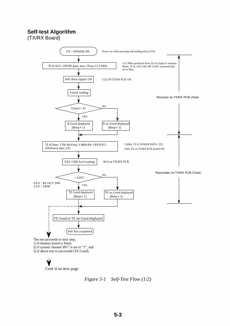
5-3
Self-test Algorithm(TX/RX Board)
TX + POWER ON
TLX/AGC: ON/RF gain: max. /Freq.:13.5 MHz
Self check signal: ON
S level reading
S level > 4?
R Good displayed (Beep
× 1)R no Good displayed
(Beep × 3)
TLX/Tone: 1700 Hz/Freq.:3 MHz/PA: OFF/EXC:ON/Power data: 255
EXC CHK level reading
> 0.8V?
TE Good displayed (Beep
× 1)TE no Good displayed (Beep
× 3)
Power on while pressing and holding down [TX].
13.5 MHz produced from 2LO is input to antenna.Mode: TLX, AGC:ON, RF GAIN: automaticallyset to Max.
U22 ON TX/RX PCB: ON
J6-6 on TX/RX PCB
YES
NO
NO
YES0.8 V : RF OUT 20W2.4 V : 140W
3 MHz, TLX, POWER DATA: 255,
Only TX on TX/RX PCB turned ON.
Receiver on TX/RX PCB check
Transmitter on TX/RX PCB Check
TE Good or TE no Good displayed
Self Test completed
The test proceeds to next step;1) if dummy board is fitted,2) if system channel 9917 is set to “1”, and3) if above test is successful (TE Good).
Cont’d on next page
Figure 5-1 Self-Test Flow (1/2)

5-4
(PA and Antenna Coupler)
Tuning operation
TE disappeared
TUNE OK
SET• jTLX/Tone• F1700Hz/Freq.3MHz/Dummy ON/Tune power data• F35TLX/Tone: 1700 Hz/Freq.3: MHz/Dummy: ON/Tune power data: 140
TX
RF level > 5?
TP Good displayed (Beep× 1)
TP no Good displayed (Beep× 3)
TP Good displayed
Self Test completed
NO
YES
SET• jTLX/Tone • F1700Hz/Freq.3MHz/Dummy ON/Tune power data• F35TLX/Tone : 1700 Hz/Freq.:3 MHz/Dummy: ON/Tune power data: 35
Reset to 3 MHz, TLX, POWER DATA: 35
RF 5: RF OUT of 30 W (RF meter reading)
Transmitter in main unitand coupler check (TUNE operation)
TP no Good displayed
Self Test completed
TP no Good displayed (Beep× 3)
From previous page
PA/FIL PCB J1-11
NO
YES
Transmitter in main unit check(with normal output power)
Figure 5-1 Self-Test Flow (2/2)
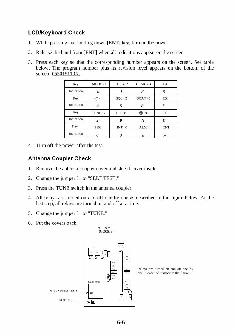
5-5
LCD/Keyboard Check
1. While pressing and holding down [ENT] key, turn on the power.
2. Release the hand from [ENT] when all indications appear on the screen.
3. Press each key so that the corresponding number appears on the screen. See tablebelow. The program number plus its revision level appears on the bottom of thescreen: 055019110X.
Key
Indication
Key
Indication
Key
Indication
Key
Indication
MODE / 1
0
4
TUNE / 7
8
2182
C
CURS / 2
1
SQL / 5
5
H/L / 8
9
INT / 0
d
CLARI / 3
2
SCAN / 6
6
A
ALM
E
TX
3
RX
7
CH
b
ENT
F
/ 4
/ 9
4. Turn off the power after the test.
Antenna Coupler Check
1. Remove the antenna coupler cover and shield cover inside.
2. Change the jumper J1 to "SELF TEST."
3. Press the TUNE switch in the antenna coupler.
4. All relays are turned on and off one by one as described in the figure below. At thelast step, all relays are turned on and off at a time.
5. Change the jumper J1 to "TUNE."
6. Put the covers back.
J1 (TUNE/SELF TEST)
S1 (TUNE)
AT-1503(05O0669)
Shield cover
K1
K2
K3
K4
K5
K6
K13
K7
K8
K9
K14
K15
K16
K17
K18
K1
2
K2
2
K2
1
K2
0
K1
9
K1
0
K11
2 5
4
3
1
Relays are turned on and off one byone in order of number in the figure.

5-6
5.3 Troubleshooting
Table 5-1 Troubleshooting Guide List
Symptom Possible Cause/Test Remedy
1 Brown in-line fuse (30A). Replace fuse.
2 Overvoltage protector (17 V) activated.Check power supply for13.6 V ± 15 %.
3Defective power switch. Disconnect powerconnector, check between J1 #1 and #2 onPA/FIL board for continuity.
Replace switch.1No power beingsupplied
4
Defective SW REG board (optional).Measure voltage between J2 #1 and #3 for12 V (input), and between J3 #1 and #3 for12 V (output).
If no input, replace PA/FILboard. If no output, replaceSW REG board.
1When getting into TX mode. Defectiverelay K1. Breaker F2 on PA/FIL boardtrips.
Replace PA/FIL board.
2 Defective PA Transistor. Replace PA Transistor, orPA/FIL board.
2Power is shutdown.
3 When connecting BK line. Check BK lines for correctwiring.
3 LCD blinks. 1 UNLOCK signal is detected; defectivePLL.
Replace TX/RX board.
4 Nothing on LCDdisplay
1 If 12 V is supplied to PA, F1 (4A) onPA/FIL board trips.
Check J2 (12 V line) onPA/FIL board for overload.
5LCD display isfreezed, orabnormal.
1Loose connection on PCB. Defective flatcable on CPU board.
Check connections. ReplaceCPU board.
1 Specific key does not work. (Carry outself-test.)
6 No key response2 All keys do not work. CR1 on CPU board
does not blink.
Replace CPU board.
1 Carry out self-test. If cannot, replace COUPboard.
2If TUNE error appears immediately afterTX, no RF signal is input to antenna cou-pler.
⋅ Check coaxial cable betweenmain unit and antenna cou-pler for discontinuity.
⋅ Check transmitter circuit inmain unit.
⋅ Check TUNE power data for40 (standard).
3 If antenna coupler does not start tuning,control circuit is defective.
⋅ Check system setting 9920.⋅ Check control signal lines
connected between main unitand antenna coupler
4If TUNE error occurs on specific band,antenna and/or grounding is abnormal.
Check antenna and groundwire connection. If OK, try tochange antenna length.
5
If tuning is unstable on specific band, an-tenna and/or grounding is abnormal, ormatching relay in antenna coupler is de-fective.
⋅ Check antenna and groundwire connection. If OK, tryto change antenna length.
⋅ Replace COUP board.
7 TUNE error
6If frequency range in which TUNE erroroccurs is the same as that of a TX filter,TX FIL circuit is defective.
Replace PA/FIL board.

5-7
Symptom Possible Remedy
1-1 Carry out self-test. If TE is NG, TX signalis not output from TX/RX board. Replace TX/RX board.
1-2 Carry out self-test. If TP is NG, TX signalis not output from PA/FIL board. Replace PA/FIL board.
2Carry out self-test. If TE is good and nosignal is emitted on all bands, PA transistoris defective.
Replace PA/FIL board or PAtransmitter(s).
8 Abnormaltransmission
3Carry out self-test. If TE is good and nosignal is emitted on specific band, powerdata is incorrect.
Check power data for 220(standard).
1 Carry out self-test. If R is NG, receivercircuit on TX/RX board is defective.
Replace TX/RX board.
2-1
If sensitivity is low on all bands, checkmain unit with antenna coupler discon-nected. If main unit is OK, antenna coupleror antenna is defective.
Check antenna. ReplaceCOUP board.
2-2
If sensitivity is low on all bands, checkmain unit with antenna coupler discon-nected. If main unit is NG, RX RF circuitis defective.
Replace TX/RX board.
2-3 If sensitivity is low on specific band, FILcircuit on PA/FIL board is defective.
Replace PA/FIL board.
3 Sensitivity is very low on less than 1.6MHz.
Check jumper setting of J8/J9for 2: 0.1 to 30 MHz.
4 No receiving sound on specific emissionmode (Defective demodulation circuit) Replace TX/RX board.
5 No TLX receiving sound IF FIL (0.4 k) is not fitted onTX/RX board.
6 No sound from either internal or externalspeaker Replace the speaker.
7No receiving sound from both internal andexternal speakers (Receiver AF circuit U15is defective.)
Replace TX/RX board.
9 Abnormal reception
8 Heavy external noise.Find noise source by turningon other equipments one at atime.
RF meter reading vs output power
RF meter reading 0 1 2 3 4 5 6 7 8 9 10 11
Output power (W) 0 + 2 10 15 30 40 50 60 67 72 75 <

5-8
5.4 Measurement
CAUTION: Do not turn any adjusters until you understand their functions. Usecalibrated measuring instruments.
1. Frequency Adjustment
Note) Allow a frequency counter for enough warm-up time.
1. Turn on the FS-1503, and leave it for more than 3 minutes.
2. Connect a frequency counter to 2 nd Local oscillator output, TP3 (H) and TP4 (C) onthe TX/RX board.
3. The reading must be 54 MHz ± 10 Hz. If not, adjust C554.
FAN
VCO
DDS
TX/RX Board (05P0666)
C554: Freg. Adj.
Y501: REF. X'tal 36.0 MHz
TP4 (GND)
TP3 (54 MHz)
Front Panel
U25 (NB PCB)
Figure 5-2 Frequency Adjustment

5-9
CAUTION: Do not transmit during the measurement on receiver circuit, otherwise SSGmay be damaged.
2. J3E Receiver Gain
1. Make the connection as below.
SSG 50ΩANT
( 50Ω coax.) FS-1503
EXT SP
(H)
(C)
4 Ω or 8Ω
13.6 V
Milli-voltmeter
oscilloscope
Figure 5-3 Measurement on RX Circuit
2. Set the FS-1503 as below.⋅ RF GAIN: Maximum⋅ RX Freq.: 4.0 MHz, MODE: J3E, AGC: on⋅ AF GAIN: 50 % of rated noise output (100 mVrms for 4-ohm speaker, 200 mVrmsfor 8-ohm speaker)
3. Applying 4.0 MHz + 1.0 kHz signal from the SSG, adjust the SSG output level sothat the ratio between AF output and noise output is 20 dB. The output should be lessthan 3 dBµV.With a 8 ohm speaker connected, the S/N is 20 dB when AF noise output is 200mVrms and AF signal output is 2 Vrms.
3. J3E AGC Adjustment
1. Make a connection as shown in figure 5-3.
2. Set the FS-1503 as below.⋅ RF GAIN: Maximum⋅ RX Freq.: 4.0 MHz, MODE: J3E, AGC: on⋅ AF GAIN: adequate AF output
3. Applying 4.0 MHz + 1.0 kHz signal from the SSG, adjust the SSG output level sothat the S meter start deflecting. The output shoule be +10 dBµV. If not, adjust R210on the TX/RX board.
SSG Output Level vs. S-meter Reading
SSG Output(dBµV)
10 20 30 40 50 60 70 80 90 100
S-meter + (1) 4 5 5 to 6 6 to 7 7 8 8 to 9 10 11

5-10
4. J3E RX Total Gain
1. Make a connection as shown in figure 5-3.
2. Set the FS-1503 as below.⋅ RF GAIN: Maximum⋅ RX Freq.: 4.0 MHz, MODE: J3E, AGC: on⋅ AF GAIN: Maximum
3. Applying 4.0 MHz + 1.0 kHz signal from the SSG, adjust the SSG output level sothat the AF output level is 1W.The output should be –5 to + 1dBµV.(Rated output; 2Vrms for 4-ohm speaker; 2.83Vrms for 8-ohm speaker)
5. J3E TX Output Power
Refer to 4.4 Power Data Setting in chapter 4 for power adjustment.
1. Make a connection as below.
50 Ω Pwr meter 50ΩANT
(50Ω Coax.)FS-1503
AF OSC
MIC(H)
(C)
13.6 VAF OSC
ATT
200Ω
200Ω
200Ω
600Ω + 6 dBm
600Ω+6 dBm
600Ω– 46 dBm
3412
PTT SW
(GND)(PTT)
oscilloscope
Figure 5-4 Measurement of TX output power
2. Set the measuring instrument as below.AF Oscillators: one for 1000 Hz and another for 1600 Hz, output level of +6 dBmAttenuator: 46dB or microphone input of –46 dBm
3. While pressing the PTT switch down, read the power meter. (Output power meas-urement with two tone signal) Double the reading for peak-to-peak power(Px).
References)1) J2B(EIB): Power is measured by applying 0dB, 600 ohm.2) NBDP : Measured in FEC-C mode.3) DSC : Measured by transmitting DOT signal.

5-11
5.5 How to Change PA Transistor
CAUTION: Apply a thin coating of silicone grease to transistor 2SC3240. Thegrease aids the transfer of heat from the transistor to the chassis. Before wiring,transistor must be fixed to the chassis securely.
The PA bias must be checked after replacing the PA transistor.
1. Disconnect "PA IN" connector.
2. Make a open circuit on FL3 and connect a DC current meter.
3. While pressing the PTT switch down, adjust R39, PA BIAS so that the meter reads450 to 550 mA.
SW REG PA/FIL Board(05P0667)
Front Panel
K1
T4
FL3
PA BIAS
(FIL circuit)
(PA circuit)Q6
Q7
Q4
Q5U3
R69 0.22ΩQ4/5 BIAS: 40 to 60 mV
Q6/7 BIAS Adj.: 500 mA ± 50 mA measured at FL3R39
PADRIVE PA BIAS measurement(Cut copper foil)
DC currentmeter
+ –
FL3
500 mA ± 50 mA
PA IN
Figure 5-5 PA Circuit
Collector bias of Q4 and Q5 measured across R69, 0.22 ohm is 40 to 60 mA normally.

5-12
5.6 Measurements and Adjustment
CAUTION: Do not turn any adjusters until you understand their functions. Themeasuring instruments must be calibrated before using.
Electrical Shock Hazard:This equipment contains high voltages which can cause death at several internal circuits. Any internal adjustment, servicing and repair shall only be perfomed by qualified service personnel totally familiar with electrical circuits and servicing of the equipment. A residual charge remains in capacitors and other devices several minutes after turning off the power.It is therefore essential to wait at least 3 minutes to allow residual charge to subside before acceessing the inside of the equipment.
DANGER
1. Adjustment
Table 5-2 Adjustment (1/2)
Board Item Setting Adjuster Check Point Level Remarks
Overvoltageprotector
Input voltage: 17.0 to18.5 V
- - Power: off
PAtemperature Temperature: 25 °C - J1 #7 (H) and
9 (C) 1.0 ± 0.1 V
DRIVETR (Q4/Q5)BIAS
Disconnect[EXC IN], PTT ON - R69 40 to 60 mV
PA/FIL(050667)
PA TR(Q6/Q7)BIAS
Disconnect[EXC IN], PTT ON R39 FL3 500 mA ±
50 mA
CPU(05P0665)
ContrastAdj. - R1 TP1 (H) and
TP2 (C) 3.3 ± 0.05 VUse high Zvoltmeter.
Outputpower Adj. Input voltage: 13.6 V R15 J2 #1 (H) and
3 (C) 13.0 VSW REG(05P0668) Oscillation
Freq Adj. Input voltage: 13.6 V -TP1 (H) andTP2 (C)
170 kHz ±20 kHz(22 Vpp)
Optional
COUP(05P0669)
Phase Det.BalanceAdj.
- R24 - Mid. pointMay be changedto fixed resistor

5-13
Table 5-2 Adjustment (2/2)
Board Item Setting Adjuster Check Point Level Remarks
OSC Circuit
54 MHz ±1 HzRef. OSC,
Frequency30 minutes afterpower-on C554
TP3 (H) -TP4 (C) 1.1 Vp-p to
1.5 Vp-p
2Lo output(54 MHz)
3rd LocalOSC.
MODE: J3E - TP7 (H) -TP6 (C)
more than1.0 Vp-p
456.5 kHz
1st LocalOSC.
MODE: TLX - TP1 (H) -TP2 (C)
0.8 Vp-p to1.2 Vp-p
Fo +54.455 kHz
RX circuit
S-meter RX SIG: 4 MHz/J3E R210 S meter +10 dBµV SSG Level
S/N RatioRX SIG: 4 MHz/J3ERF GAINMAX/AGC ON
- - +2 dBµV ??SSG Level
(S/N = 20 dB)
Total GainRX SIG: 4 MHz/J3EFR/AF GAINMAX/AGC ON
- -+1 to-5 dBµV
SSG Level(AF output of1 W)
NBFunction
External pulse noisemixed
CR11/12 (A) -GND
Negativepulse
LINE OUTLevel
RX SIG: 4 MHz/TLXRF GAIN MAX/AGC ON
REMOTEConnector10 (H) -11 (C)
+3 to +9 dBm 600 Ω Load
TX Circuit
MIC GAIN MIC IN: 600 Ω/-40 dBm/1500 Hz
-TP8 (H) -TP9 (C)
1.6 ±0.2 Vp-p
MIC IN: 600 Ω/-40 dBm/1500 Hz
R156TP5 (H)-TP6 (C) 0.4 Vp-p
TX GAINAdjustment
MIC IN: 600 Ω /-54 dBm/1500 Hz4 MHz/J3E/P.Data:220
R156 Output frommain unit 40 W
OutputLevel
2-TONE ALM:[ALM] + [ENT]4 MHz/J3E/P.Data:220
-J2(EXC OUT) about 20 Vp-p OUT 50 Ω
Load
H3E MODAdjustment
MIC IN: -40 dBm/600 Ω /1500 Hz2182 kHz/H3E/P.Data: 200
R101 Output frommain unit 100 % MOD
TX/RX(05P0666)
LINE INLevel
LINE IN: 0 dBm/1700 Hz4 MHz/ TLX/P.Data: 220
-J2(EXC OUT) about 20 Vp-p OUT 50 Ω
Load

5-14
Electrical Shock Hazard:This equipment contains high voltages which can cause death at several internal circuits. Any internal adjustment, servicing and repair shall only be perfomed by qualified service personnel totally familiar with electrical circuits and servicing of the equipment. A residual charge remains in capacitors and other devices several minutes after turning off the power.It is therefore essential to wait at least 3 minutes to allow residual charge to subside before acceessing the inside of the equipment.
DANGER
2. Measurement
*Setting Details
A MIC IN: -40 dBm/1500 Hz/600 Ω, 4 MHz/J3E/Power Data 220
B PTT ON (No AF signal)
C Receiving mode
D SSG: 100 dBµV/50 Ω, 4MHz/J3E
E MIC IN: -40 dBm/1500 Hz/600 Ω, 4 MHz/J3E/Low Power Data 140
Table 5-3 Measurements (1/2)
Board Name Check Points *Setting Reading Remarks
T1 Input A 14 Vp-p [PA IN]: J4
Q4/5: B-GND 2 Vp-p
C-GNDA
15 Vp-p
Q4/5: B-GND 0.68 Vdc
C-GNDB
13 Vdc
DRIVE (2SC3133)
Q6/7: B-GND 4 Vp-p
C-GNDA
25 Vp-p
Q6/7: B-GND 0.6 +Vdc
C-GNDB
13 Vdc
PA (2SC3240)
C33 OUT A 250 Vp-p PA OUT
ANT A 250 -Vp-p 50 Ω Load
J1 #10 (ALC) A 4.2 Vdc ALC CONT
PA/FIL(05P0667)
U1-1 (Gate) C 2.3 Vdc Overvoltage protector(Input: 13.6 V)

5-15
Table 5-3 Measurements (2/2)
Board Name Check Points *Setting Reading Remarks
TX Circuit
EXC OUT A 14 Vp-p PA connected
CHK EXC A 2.4 Vdc CR24-K
Q25: B-GND 0.5 Vp-p
C-GNDA
15 Vp-p
Q25: B-GND 0.65 Vdc
C-GNDB
13 Vdc
2SC3133
TP5 - TP6 0.65 Vp-p 1 MIX MOD AF Input
TP8 - TP9A
13 Vp-p MIC Input
OSC Circuit
TP1 - TP2 C 0.8 Vp-p 1 Lo (Fo + 54.455 MHz)
TP3 - TP4 C 1.1 Vp-p 2 Lo (54 MHz)
TP7 - TP6 C 1.0 Vp-p 3 Lo (456.5 kHz)
RX Circuit
Q1/2: D-GND 1.2 Vp-p RX RF FET (2SK937)
S-GNDD
0.11 Vp-p
Q1/2: D-GND C 13 Vdc RX RF FET (2SK937)
S-GND C 2 Vdc
U3-7RF VRMAX toMIN
4.2 Vdc to5.6 Vdc AGC
U15-1 1.2 Vdc
-2 0.8 Vdc
-3 0 Vdc
-4 6.0 Vdc
TX/RX (05P0666)
-5
D
13 Vdc
AF Power AMP (TDA2003H)*Use high Z voltmeter.
TP1 - TP2 22 Vp-p 170 kHzSW REG(05P668) Q1: G-TP2
Input:13.6 V 14 Vp-p 2SK1266 (GATE)
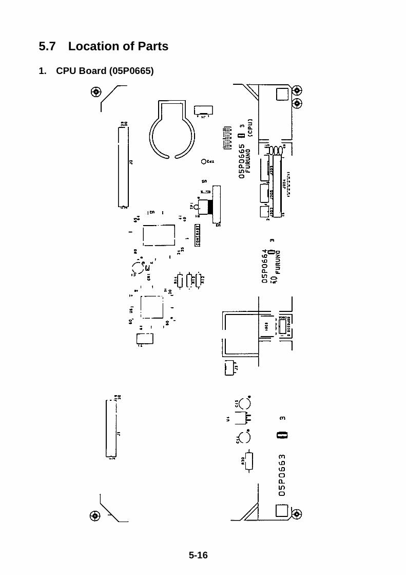
5-16
5.7 Location of Parts
1. CPU Board (05P0665)


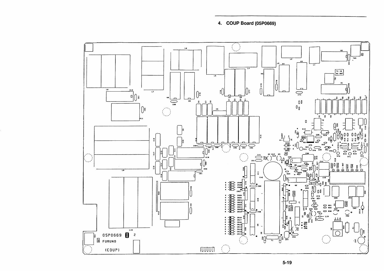
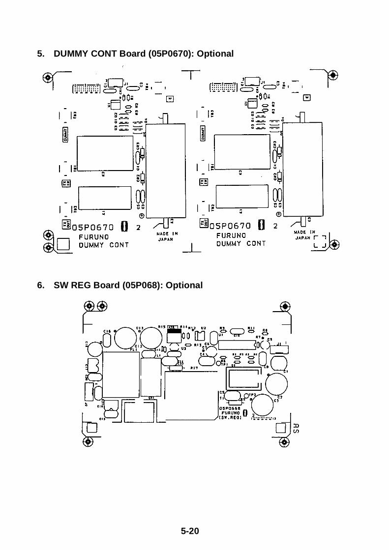
5-20
5. DUMMY CONT Board (05P0670): Optional
6. SW REG Board (05P068): Optional
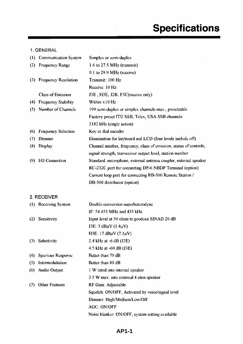
AP1-1

AP1-2

AP1-3

AP2-1

AP2-2

AP2-3

AP2-4

AP2-5

AP2-6
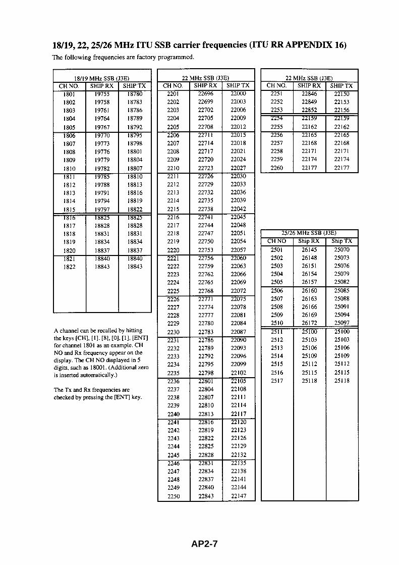
AP2-7
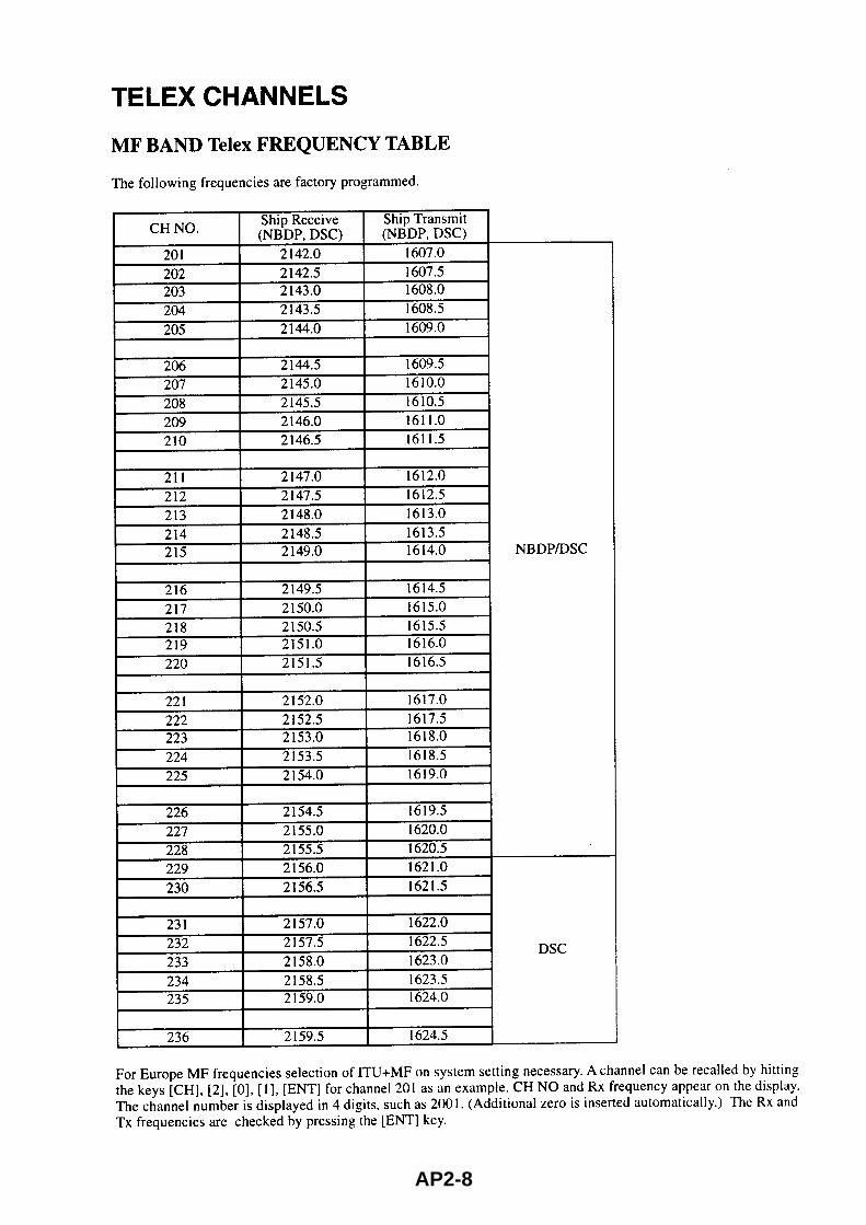
AP2-8

AP2-9
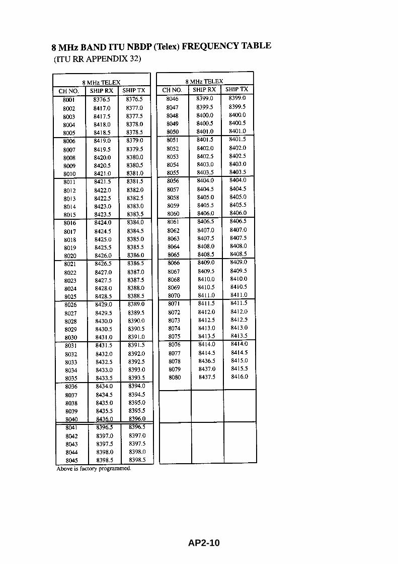
AP2-10

AP2-11

AP2-12

AP2-13

AP2-14

AP2-15

AP2-16


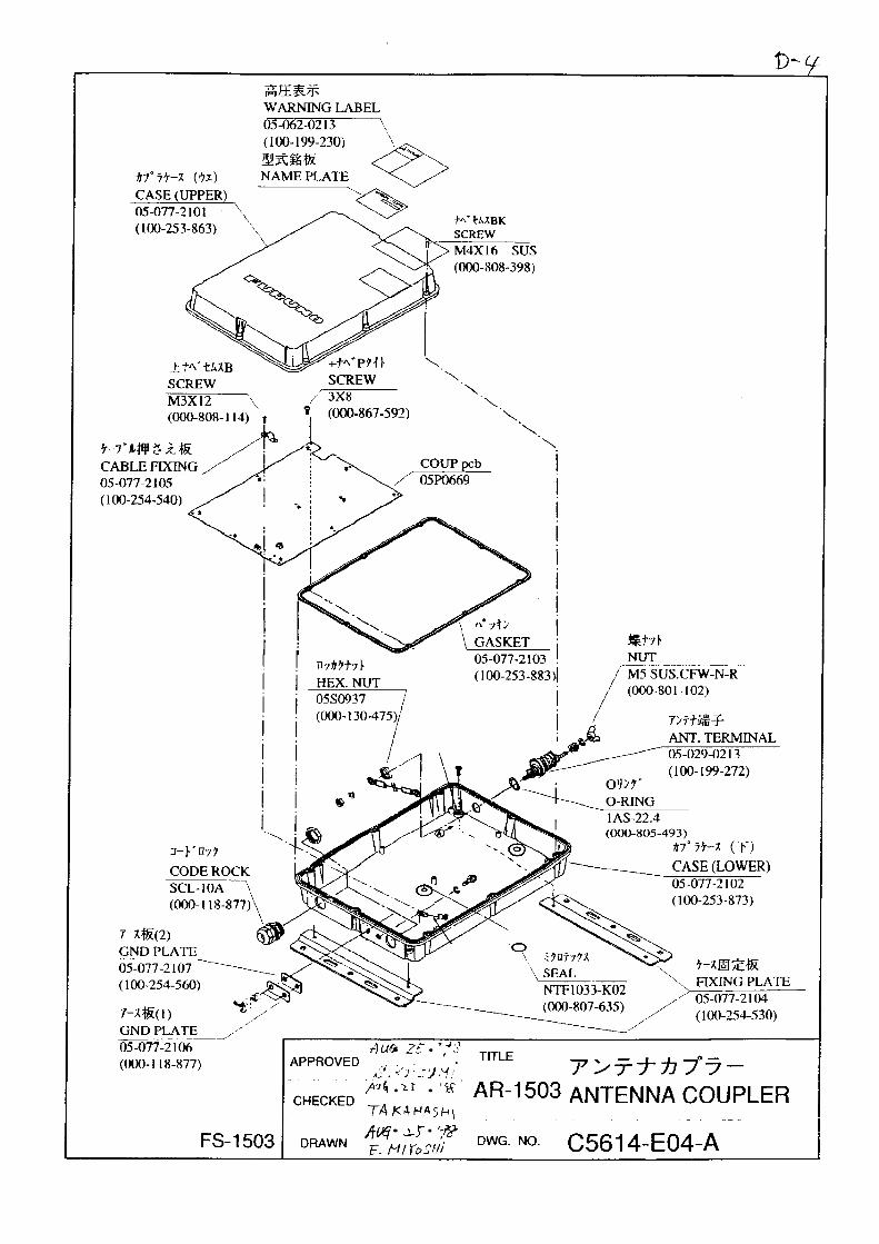


S-0
Board Name Type Dwg. No. Page
Outline Drawing FS-1503 C5614-G01 S-1
Outline Drawing AT-1503 C5614-G02 S-2
Outline Drawing RP-270 C5485-031 S-3
Outline Drawing PC-220 C5485-029 S-4
Interconnection Diagram E5614-C01 S-5
FS-1503 General Ckt FS-1503 C5614-K01 S-6
CPU 05P0665 C5614-K07 S-7
050666 (1/2) C5614-K04 S-8TX/RX
05P0666 (2/2) C5614-K05 S-9
NB DET 05P0466 C5548-K12 S-10
CONTROL 05P0459 C5548-K11 S-11
REMOTE (A) 05P0457 C5548-K08 S-12
REMOTE (B) 05P0458 C5548-K09 S-13
PA/FIL 05P0667 C5614-K06 S-14
SW REG 05P0668 C5614-K03 S-15
AT-1503 General Ckt AT-1503 C5614-K02 S-16
COUP 05P0669 C5614-K08 S-17
DUMMY CONT 05P0670 C5614-K09 S-18
AC Power PR-270 C5485-032 S-19
DC-DC Converter PC-220 C5485-030 S-20
Contents of Drawings
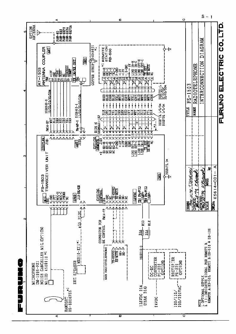

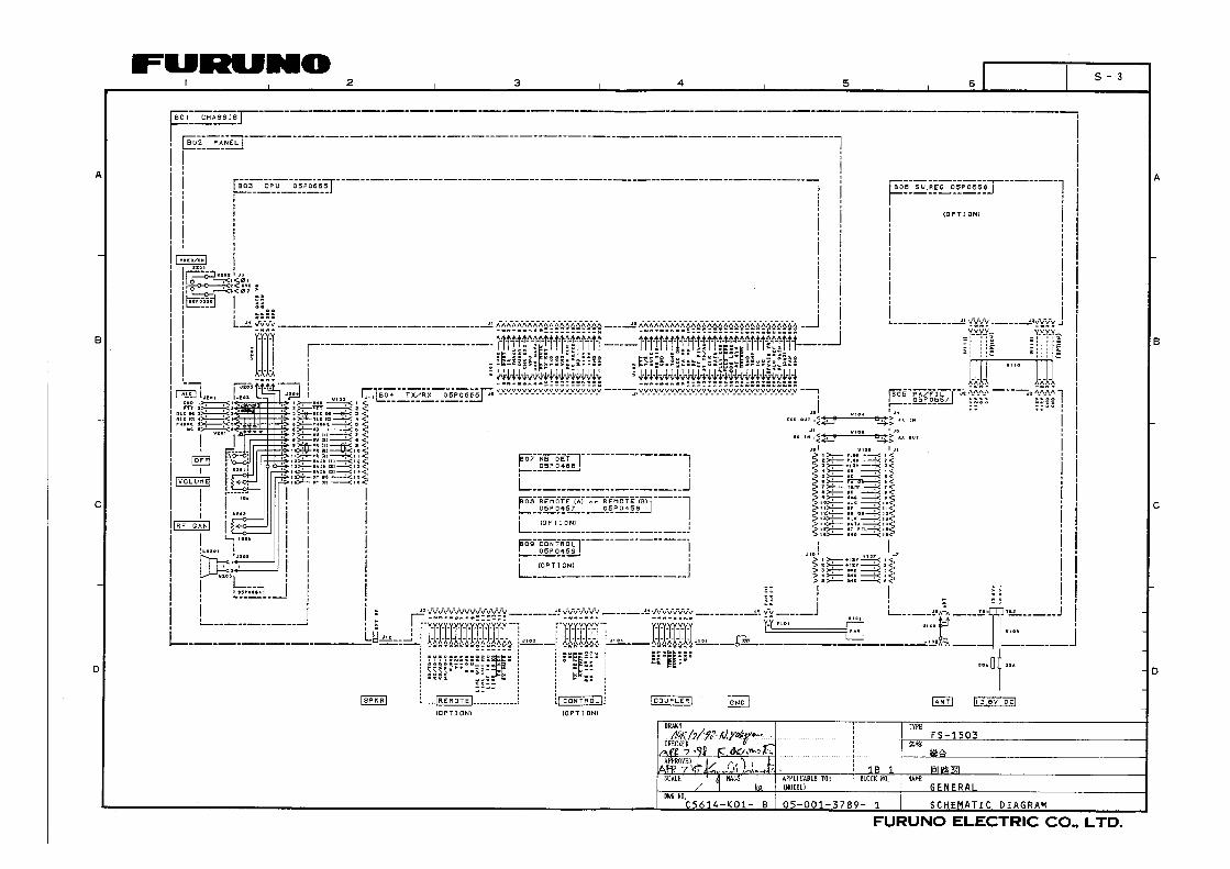


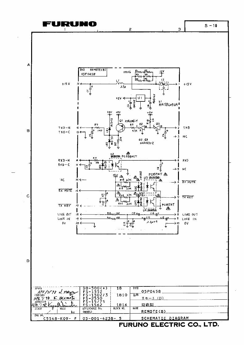


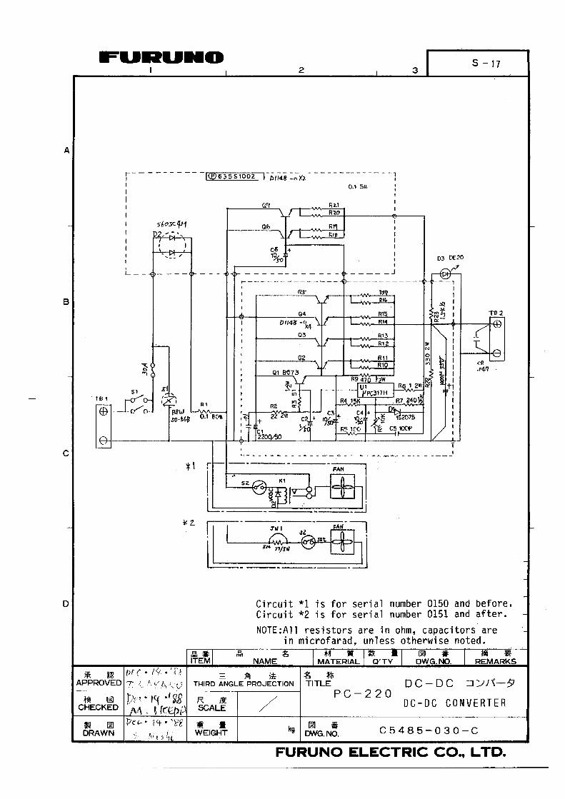


2/3 When PA transistor 2SC2879A, (005-376-690, Code number for 2 pcs.) is used on 05P0667 board, add C27 (DM15C331J5, 000-154-416) across the primary winding of T2 as shown in Figs.1 and 2. If C27 is already fitted, change it to 330 pF. The PA transistor, 2SC2879A does not require an insulator. (Related Furuno Information: FQ5-2004-036)
Fig.1 C27, 330 pF on 05P0667 with 2SC2879A
Fig.2
Fig.3 PA Cooling Fan in the upper shield plate
C27 added on 05P0667
Transistor C27 2SC2879A 330 pF SD1487 None or
about 150 pF

Fig.4 PA/FIL board,05P0667A
Fig.6 CPU board, 05P0665A and PANEL board, 05P0664A
Fig.5 TX/RX board,05P0666B/C
PANEL board
No shield cover
CPU board
New TX/RX board has noshield cover for PLL circuit.
3/3
PA Transistors, 2SC2879A