SRF LIMITATIONS - University of Manchester
89
Page 1 Jean Delayen Center for Accelerator Science Old Dominion University and Thomas Jefferson National Accelerator Facility SRF LIMITATIONS COCKCROFT INSTITUTE, DARESBURY JULY 2010
Transcript of SRF LIMITATIONS - University of Manchester

Page 1
Jean Delayen
Center for Accelerator ScienceOld Dominion University
andThomas Jefferson National Accelerator Facility
SRF LIMITATIONS
COCKCROFT INSTITUTE, DARESBURY JULY 2010

Page 2
Outline
• Residual resistance
• Multipacting
• Field emission
• Quench
• High-field Q-slope

Page 3
The Real World
11
10
9
80 25 50 MV/m
Accelerating Field
Residual losses
Multipacting
Field emission
Thermal breakdown
Quench
Ideal
RF Processing
10
10
10
10
Q

Page 4
Losses in SRF Cavities
• Different loss mechanism are associated with different regions of the cavity surface
Electric field high at iris
Magnetic field high at equator
Ep/Eacc ~ 2
Bp/Eacc ~ 4.2 mT/(MV/m)
Page 5
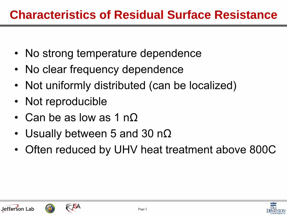
Characteristics of Residual Surface Resistance
• No strong temperature dependence• No clear frequency dependence• Not uniformly distributed (can be localized)• Not reproducible• Can be as low as 1 nΩ• Usually between 5 and 30 nΩ• Often reduced by UHV heat treatment above 800C

Page 6
Origin of Residual Surface Resistance
• Dielectric surface contaminants (gases, chemical residues, dust, adsorbates)
• Normal conducting defects, inclusions• Surface imperfections (cracks, scratches,
delaminations)• Trapped magnetic flux• Hydride precipitation• Localized electron states in the oxide (photon
absorption)
Rres is typically 5-10 nΩ at 1-1.5 GHz

Page 7
Trapped Magnetic Field
A parallel magnetic filed is expelled from a superconductor.
What about a perpendicular magnetic field?
The magnetic field will be concentrated in normal cores where it is equal to the critical field.

Page 8
Trapped Magnetic Field

Page 9
Trapped Magnetic Field
• Vortices are normal to the surface• 100% flux trapping• RF dissipation is due to the normal
conducting core, of resistance Rn
2
ires n
c
HR RH
≅ Hi = residual DC magnetic field
• For Nb:
• While a cavity goes through the superconducting transition, the ambient magnetic filed cannot be more than a few mG.• The earth’s magnetic shield must be effectively shielded.• Thermoelectric currents can cause trapped magnetic field, especially in cavities made of composite materials.
0.3resR ≈ Ω to 1 n /mG around 1 GHzDepends on material treatment

Page 10
Trapped Magnetic Field
A fraction of the material will be in the normal state.
This will lead to an effective surface resistance
For Nb:
While a cavity goes through the superconducting transition, the ambient magnetic filed cannot be more than a few mG.
The earth’s magnetic shield must be effectively shielded.
In cavities made of composite materials, thermoelectric currents can cause trapped magnetic field.
/ cH H
( )/n cH Hr
0.5 to 1 n /mG around 1 GHzeffr ª W

Page 11
Trapped Magnetic Field

Page 12
Rres Due to Hydrides (Q-Disease)• Cavities that remain at 70-150 K for several hours (or slow cool-down, < 1
K/min) experience a sharp increase of residual resistance
• More severe in cavities which have been heavily chemically etched

Page 13
Hydrogen: “Q-disease”
• H is readily absorbed into Nbwhere the oxide layer is removed (during chemical etching or mechanical grinding)
• H has high diffusion rate in Nb, even at low temperatures.
• H precipitates to form a hydride phase with poor superconducting properties: Tc=2.8 K, Hc=60 G• At room temperature the required
concentration to form a hydride is 103-104 wppm
• At 150K it is < 10 wppm

Page 14
Cures for Q-disease
• Fast cool-down
• Maintain acid temperature below 20 °C during BCP
• “Purge” H2 with N2 “blanket” and cover cathode with Teflon cloth during EP
• “Degas” Nb in vacuum furnace at T > 600 °C

Page 15
Q0 Record

Page 16
Multipacting
• No increase of Pt for increased Pi during MP• Can induce quenches and trigger field emission

Page 17
Multipacting
Multipacting is characterized by an exponential growth in the number of electrons in a cavity
Common problems of RF structures (Power couplers, NC cavities…)
Multipacting requires 2 conditions:
• Electron motion is periodic (resonance condition)
• Impact energy is such that secondary emission coefficient is >1

Page 18
One-Point Multipacting
One-point MP
Cyclotron frequency:
Resonance condition: Cavity frequency ( g) = n x cyclotron frequency
Possible MP barriers given by
n: MP order
The impact energy scales as2 2
2g
e EK
mω⊥∝
+ SEY, δ(K), > 1 = MP
Empirical formula: [ ] [ ]00.3Oe MHznH fn
=

Page 19
Two-Point Multipacting
Empirical formula:
[ ] [ ]00.6Oe MHz
2 1nH fn
=−

Page 20
Two-Side Multipacting

Page 21
Multipacting Simulatiom

Page 22
Secondary Emission in Niobium

Page 23
Secondary Emission in Niobium

Page 24
MP in SRF Cavities
Early SRF cavity geometries (1960s-’70s) frequently limited by multipacting, usuallyat < 10 MV/m
“Near pill-box” shape

Page 25
MP in SRF Cavities
Electrons drift to equatorElectric field at equator is 0
MP electrons don’t gain energyMP stops350-MHz LEP-II cavity (CERN)
“Elliptical” cavity shape (1980s)

Page 26
Cures for Multipacting
• Cavity design
• Lower SEY: clean vacuum systems (low partial pressure of hydrocarbons, hydrogen and water), Ar discharge
• RF Processing: lower SEY by e- bombardment (minutes to several hours)

Page 27
Recent Examples of Multipacting
1.E+09
1.E+10
1.E+11
0 2 4 6 8 10 12 14 16 18 20
Qo
E (MV/m)
SNS HB54 Qo versus EaccMultipacting limited at 16MV/m 5/16/08 cg 2008
MPField
emission

Page 28
Field Emission• Characterized by an exponential drop of the Q0
• Associated with production of x-rays and emission of dark current
1.E+09
1.E+10
1.E+11
0 5 10 15 20
Qo
E (MV/m)
SNS HB54 Qo versus Eacc
0
0
0
0
1
10
100
1000
10000
0 5 10 15 20 25
mR
em/h
r)
E (MV/m)
SNS HTB 54 Radiation at top plate versus Eacc 5/16/08 cg

Page 29
DC Field Emission from Ideal SurfaceFowler-Nordheim model
6 2 9 3/21.54 10 6.83 10exp
: )::
2 Current density (A/m Electric field (MV/m) Work function (eV)
EJE
JE
- Ê ˆ¥ ¥ F= -Á ˜F Ë ¯
F

Page 30
Field Emission in RF Cavities
Acceleration of electrons drains cavity energy
Impacting electrons produce:• line heating detected by
thermometry • bremsstrahlung X rays
Foreign particulate found at emission site
FE in cavities occurs at fields that are up to 1000 times lower than
predicted…
5/26 9 3/21.54 10 ( ) 6.83 10exp
::
Enhancement factor (10s to 100s) Effective emitting surface
k EJE
k
bb
b
- Ê ˆ¥ ¥ F= -Á ˜F Ë ¯

Page 31
How to Investigate Field EmissionFE in SC Cavity
Electron trajectory T-map
Dissection and analysis

Page 32
Dissection and SEM

Page 33
C, O, Na, In Al, Si
Stainless steel
Melted
Melted
Melted
Example of Field Emitters

Page 34
DC Field Emission Microscope
Carbon Carbon
Emission Current

Page 35
Type of Emitters
Smooth nickel particles emit less or emit at higher fields.
Ni
V
•Tip-on-tip model explains why only 10% of particles are emitters for Epk < 200 MV/m.

Page 36
Tip-on-tip Model
• Smooth particles show little field emission
• Simple protrusions are not sufficient to explain the measured enhancement factors
• Possible explanation: tip-on-tip (compounded enhancement)

Page 37
FE onset vs. Particulate Size
Page 38
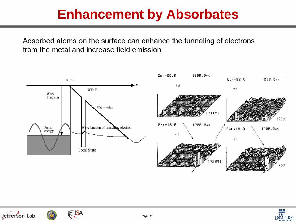
Enhancement by Absorbates
Adsorbed atoms on the surface can enhance the tunneling of electrons from the metal and increase field emission

Page 39
Intrinsic FE of Nb
Single-crystal Nb samples showed FE onset higher than 1 GV/m.
The work function was obtained from the I-V curves:
Φ = 4.05 ± 17% eV for Nb (111)Φ = 3.76 ± 27% eV for Nb (100)

Page 40
Cures for Field Emission
• Prevention:– Semiconductor grade acids and solvents– High-Pressure Rinsing with ultra-pure water– Clean-room assembly– Simplified procedures and components for
assembly– Clean vacuum systems (evacuation and venting
without re-contamination)
• Post-processing:– Helium processing– High Peak Power (HPP) processing

Page 41
Helium Processing
• Helium gas is introduced in the cavity at a pressure just below breakdown (~10-5 torr)
• Cavity is operating at the highest field possible (in heavy field emission regime)
• Duty cycle is adjusted to remain thermally stable
• Field emitted electrons ionized helium gas
• Helium ions stream back to emitting site
– Cleans surface contamination
– Sputters sharp protrusions

Page 42
Helium Processing

Page 43
Helium Processing
Copper

Page 44
Helium Processing in CEBAF

Page 45
Helium Processing in CEBAF

Page 46
Practical Limitations (CEBAF)

Page 47
High Peak Power Processing
Power = 1.5 MWPulse Length = 250 us

Page 48
High Peak Power Processing
local melting leads to formation of a plasma and finally to the explosion of the emitter→ “star bursts” caused by the plasma

Page 49
High Peak Power Processing
For field emission free
Ep (pulsed) = 2×Ep (cw)

Page 50
High Peak Power Processing
1 - C48 2 - S34 3 - AC57 4 - AC56 5 - AC55 6 - AC59 7 - Z52 8 - AC640
5
10
15
20
25
30
35
PW
R
PW
R
Module 4
PW
R
EACC [M
V/m
]
Cavity
Cryostat tests: Vertical Horizontal

Page 51
Issues with HPP
• Reduced Q0 after processing• No experience with HPP above
Eacc = 30 MV/m in 9-cell cavities• Very high power required

Page 52
Thermal Breakdown (Quench)
1 4log(ΔT [mK])
Localized heating
Hot area increases with field
At a certain field there is a thermal runaway, the field collapses
• sometimes displays a oscillator behavior
• sometimes settles at a lower value
• sometimes displays a hysteretic behavior

Page 53
Thermal Breakdown
Thermal breakdown occurs when the heat generated at the hot spot is larger than that can be transferred to the helium bath causing T > Tc: “quench” of the superconducting state

Page 54
Quench Mechanism

Page 55
Thermal Breakdown: Simple Model
Heat flow out through a spherical surface:
24 2 TTr Qr
π κ ∂− =∂
Breakdown field given by(very approximately):
4 ( )T c btb
d d
T THr R
k -=
T: Thermal conductivity of NbRd: Defect surface resistanceTc: Critical temperature of Nb
Tb: Bath temperature

Page 56
Thermal Conductivity of Nb
RRR is the ratio of the resistivity at 300K and 4.2K (300 )
(4.2 )KRRRK
rr
=
RRR is related to the thermal conductivity
For Nb: ( 4.2 ) / 4 ( )-1 -1W. m . KT K RRRl = ª

Page 57
Numerical Thermal Model Calculations
Note: Htb has nearly no dependence on TB < 2.1 K

Page 58
Magneto-thermal Breakdown• Quench location identified by T-mapping• Morphology of quench site reproduced by replica technique
Local Magnetic Field Enhancement:Quench when β H > Hc

Page 59
Magneto-thermal Breakdown: Maximum Eacc
( ),max c RF
accm p acc
r HE d
H Eβ=
r 1, reduction of the local critical field within the penetration depth, due to impurities or lattice imperfectiond, thermal stabilization parameter √κβm > 1, geometric field enhancement factor

Page 60
Type of Defects
Cu
0.1 – 1 mm size defects cause TBSurface defects, holes can also cause TB
No foreign materials found

Page 61
Optical Inspection

Page 62
Defects Seen by Optical InspectionDESY

Page 63
Defects Seen by Optical InspectionDESY

Page 64
Cures for Quench• Prevention: avoid the defects
– High-quality Nb sheets– Eddy-current scanning of Nb sheets
– Great care during cavity fabrication steps
• Post-treatment:– Thermally stabilize defects by increasing the RRR– Remove defects: local grinding

Page 65
Post-purification for Higher RRR
Disadvantages:• > 50 μm material removal necessary
after heat treatment• Significant reduction of yield strength of
the Nb

Page 66
Post-purification

Page 67
Post-purification

Page 68
How High of RRR Value is Necessary?
100 μm diameter nc
defect
9-cell ILC cavities

Page 69
Defect Repair: Local Grinding
Polymond + water for grinding
Polymond: diamond particles in a resin (particle size = 40 ~ 3 um)

Page 70
Defect Repair: Local GrindingBefore Grinding
Bump
After Grinding and EP 50um
Removed the bump
Quench at Eacc=20 MV/m

Page 71
Summary on Quench• Big improvement in Cavity fabrication and treatment
less foreign materials found (at limitations <20MV/m only)
• Visual inspection systems are available• Many irregularities in the cavity surface are found with this systems
during and after fabrication and treatmentpits and bumpsweld irregularities
• Often one defect limits the whole cavity• Some correlations are found between defects and quench locations
at higher fieldsBut often no correlation between suspicious pits and bumps
and quench location• At gradient limitations in the range >30 MV/m defects are often not
identified

Page 72
High-Field Q-Slope (“Q-drop”)
11
10
9
80 25 50 MV/m
Accelerating Field
Residual losses
Multipacting
Field emission
Thermal breakdown
Quench
Ideal
RF Processing
10
10
10
10
Q
Q-drop

Page 73
Q-drop and Baking
• The origin of the Q-drop is still unclear. Occurs for all Nb material/treatment combinations
• The Q-drop recovers after UHV bake at 120 °C/48h for certain material/treatment combinations
1.5 GHz single-cell, treated by EP
No X-rays

Page 74
Experimental Results on Q-drop
JLAB
DESY
CORNELL
• “Hot-spots” in the equator area (high-magnetic field)

Page 75
Experimental Results on Q-drop
• Q-drop and baking effect observed in both TM010 and TE011 modes. TE mode has no surface electric field
Q-drop: high magnetic field phenomenon
Onset of Q-drop is higher for• smooth surfaces• reduced number of grain boundaries

Page 76
Baking: Material and Preparation DependenceBaking works on cavities made of:• Large-grain Nb (buffered chemical polished or electropolished)
• Fine-grain Nb, electropolished
Smooth surface, few grain boundaries
Smooth surface, many grain boundaries
100 μm
Baking does not work on cavities made of:• Fine-grain Nb, buffered chemical polished
Rough surface, many grain boundaries
100 μm
• Fine-grain Nb, post-purified, BCP
Smooth surface, fewer grain boundaries
50 μm

Page 77
Recipe against Q-dropRecipes necessary to overcome the Q-drop, depending on the starting material,
based on current data:
Large grain/Single crystal niobium
Fine grain niobium
BCP EP
Titanization
120 °C/12 h UHV bake
120 °C/48 h UHV bake

Page 78
Baking Effects on Low-field Rs and Hc3
r32=Bc3/Bc2: depends onbake temperature and duration
• Decrease of RBCS due to of l and of energy gap
• The physics of the niobium surface changes from CLEAN (l > 200 nm) to DIRTY LIMIT (l 25 nm ξ0)

Page 79
Models of Q-drop & Baking
• Magnetic field enhancement• Oxide losses• Oxygen pollution• Magnetic vortices

Page 80
Magnetic Field Enhancement Model
Local quenches at sharp steps (grain boundaries) when βmH > Hc
βm: Field enhancement factor
AFM image of a grain boundary edge
Q0(Bp) calculated assumingDistribution function for βm valuesThe additional power dissipated by a
quenched grain boundary is estimated to be 17 W/m
J. Knobloch et al., Proc. of the 9th SRF Workshop, (1999), p. 77

Page 81
MFE Model: Shortcomings
• Single-crystal cavities have Q-drop• Seamless cavities have Q-drop• Low-temperature baking does not change the
surface roughness• Electropolished cavities have Q-drop, in spite of
smoother surface
The model cannot explain the following experimental results:

Page 82
Interface Tunnel Exchange Model
• Interface Tunnel Exchange (ITE) model– Resonant energy absorption by quasiparticles
in localized states in the oxide layer– Driven by electric field
Schematic representation of the Nb surfaceBand structure at Nb-NbOx-Nb2O5-y interfaces
-ezE0
ezE0
0 * *rE
e zεβ
Δ>
( )0 0 0
2 2
2 20 0
12
p p pc E c E c Ec E c E c EEs
p p
c c c cR b e e e e e eE E E E
− − −− − −⎡ ⎤⎛ ⎞ ⎛ ⎞
= − + − + −⎢ ⎥⎜ ⎟ ⎜ ⎟⎜ ⎟ ⎜ ⎟⎢ ⎥⎝ ⎠ ⎝ ⎠⎣ ⎦J. Halbritter et al., IEEE Trans. Appl. Supercond. 11 (2001) p.
1864

Page 83
ITE Model: Shortcomings
• The baking effect is stable after re-oxidation• The Q-drop was observed in the TE011 mode
(only magnetic field on the surface)• The Q-drop is re-established in a baked cavity
only after growing an oxide 80 nm thick by anodization
The model cannot explain the following experimental results:

Page 84
Oxygen Pollution Model
After baking
Before baking• Surface analysis of Nb samples shows high concentrations of interstitial oxygen (up to 10 at.%) at the Nb/oxide interface• Interstitial oxygen reduces Tc and the Hc1
• The calculated O diffusion length at 120°C/48h is 40 nm
Magnetic vortices enter the surface at the reduced Hc1, their viscous motion dissipating energy
G. Ciovati, Appl. Phys. Lett. 89 (2006) 022507
Interstitial oxygen is diluted during the 120°C baking, restoring the Hc1 value for pure Nb
Calculated oxygen concentration at the metal/oxide interface as a function of temperature after 48h baking

Page 85
Oxygen Pollution Model: Shortcomings
• The Q-drop did not improve after 400°C/2h “in-situ” baking, while O diffuses beyond λ
• The Q-drop was not restored in a baked cavity after additional baking in 1 atm of pure oxygen, while higher O concentration was established at the metal/oxide interface
• Surface analysis of single-crystal Nb samples by X-ray scattering revealed very limited O diffusion after baking at 145°C/5h
The model cannot explain the following experimental results:

Page 86
Fluxons as Source of Hot-Spots
• Motion of magnetic vortices, pinned in Nb during cool-down across Tc, cause localized heating
The small, local heating due to vortex motion is amplified by RBCS, causing cm-size hot-spots
• Periodic motion of vortices pushed in & out of the Nbsurface by strong RF field also cause localized heating
Page 87
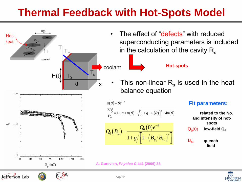
Thermal Feedback with Hot-Spots Model
• The effect of “defects” with reduced superconducting parameters is included in the calculation of the cavity Rs
Hot-spot
Hot-spots
H(t)
T Tm
T0Ts
coolant
xd • This non-linear Rs is used in the heatbalance equation
( )
( ) ( ) ( )
1
22
20
21 1 4p
b
u e
Bg u g u u
B
θθ θ
θ θ θ
−=
= + + − + + −⎡ ⎤⎣ ⎦
( ) ( )( )
00 2
0
0
1 1p
p b
Q eQ B
g B B
θ−
=⎡ ⎤+ −⎢ ⎥⎣ ⎦
related to the No. and intensity of hot-
spotsQ0(0)
Bb0
low-field Q0
quench field
Fit parameters:
A. Gurevich, Physica C 441 (2006) 38

Page 88
Q-drop: Recent Samples ResultsSamples from regions of high and low RF losses were cut from single cell cavities and examined with a variety of surface analytical methods.No differences were found in terms of:• roughness• oxide structure• crystalline orientation
It was found that “hot-spot” samples have a higher density of crystal defects (i.e. vacancies, dislocations) than “cold” samples
Hot Cold
Local misorientationangle
0 1 2

Page 89
Q-drop: Recent Samples Results
• Zero-bias conductance peak: presence of dissipative pair-breaking layers on the cavity surface• Possible source: magnetic impurities (Nb2O5-δ?)