SRAM redundancy insertion
22
May 2, 2012 1 SRAM Redundancy Insertion - Expert Prescription Required May 2, 2012 Over 20 Years Providing Complete ASIC & COT Solutions Arie Komarnitzky - Avnet ASIC Israel LTD .
-
Upload
chiportal -
Category
Technology
-
view
1.822 -
download
1
Transcript of SRAM redundancy insertion

May 2, 2012 1
SRAM Redundancy Insertion - Expert Prescription Required
May 2, 2012
Over 20 Years ProvidingComplete ASIC & COT Solutions
Arie Komarnitzky - Avnet ASIC Israel LTD.

May 2, 2012 2
• AAI introduction• SRAM redundancy• Yield considerations• Production test considerations• Design considerations• Summary
SRAM redundancy insertion - expert perscription required

May 2, 2012 3
AAI provides complete ASIC solutions for fabless & System houses. Our core business
ASIC/SoC Design and Implementation Turnkey Manufacturing
Established in 1986 – first & largest ASIC design center in Israel In the past 20 years, AAI has successfully completed more than 300
tape-outs for the Israeli ASIC market Subsidiary of Avnet Inc. - largest global technology B2B distributor Partners:
Avnet ASIC Israel In Brief

May 2, 2012 4
Deep-sub-micron (0.18u, 0.13u, 90nm, 65nm, 40nm, 28nm) System-
on-Chip implementation (design & manufacturing)
System architecture in CPU environment (ARM, MIPS, ARC)
Mixed Signal and Full Custom analog designs
IP integration and verification (ARM, MIPS, USB2.0, PCI-Ex,
DDR2/3, etc.)
Design for test: JTAG, memory BIST, SCAN insertion and ATPG
Design methodologies for low power applications
Design for manufacturability (DFM): yields, quality, reliability
Advanced assembly techniques: CSP, Flip-Chip, BGA, MCP/SIP
Test program and test hardware development and debug
AAI unique expertise

May 2, 2012 5
SRAM redundancy
Redundancy configuration
bits
D Q
EN
D Q
EN
D Q
EN
D Q
EN
D Q
EN
WEN
Din3
Din2
Din1
Din0
Dout3
Dout2
Dout1
Dout0
Redundancy concept example 4 bit register
Hard – programmed once at production test
Soft – programmed every system power up

May 2, 2012 6
• Memories are more prone to defects then other sections of SOC
• SRAM Repair – defect SRAM bits are repaired by replacing bad rows and
columns with redundant rows and columns– After repair the memory yield is aligned with the rest of the
chip– Result is more good dies per wafer
• As wafer cost is fixed, unit cost decreases• Savings from SRAM redundancy increase with volume
SRAM Redundancy - Basics

May 2, 2012 7
• SRAM redundancy insertion is DFY methodology• Some popular DFY methodologies from 40nm and
below – CAA, CMP, LPA, …• Similar to other DFY methodologies:
– Most SRAM redundancy costs are at design stage– SRAM redundancy gains are from production
• volume dependent• delayed
• ROI calculation is required for SRAM redundancy go/no go decision
SRAM redundancy – DFY (Design for Yield)

May 2, 2012 8
Possible costs at design stage• dedicated IP:
– SRAM compiler with redundant rows and columns– BIST tools supporting redundancy– FUSE/EFUSE/OTP or Soft Repair
• design time, spec degradation and schedule impactAddition to unit cost• area• production test time
SRAM redundancy – Costs

May 2, 2012 9
SRAM redundancy ROI - Example
Design1st Yr2nd Yr3rd YrWafer cost $ 5,000
Volume forcast0 10,000
100,000 1,000,000 Die size [mmsq]100
SRAM Compiler- $ 100,000 Gross die per wafer729
BIST tool- $ 100,000 natural yield70%
FUSE IP- $ 100,000 Net die per wafer510
Design overhead- $ 100,000 net die area unit cost before repair $ 9.80
TP develop overhead - $ 100,000 Repair yield90%
Tester additional cost - $
- $
556 - $
5,556 - $ 55,556 Redundancy and BIST area overhead10%
Gain from repair - $
$ 13,293
$ 132,935 $ 1,329,345 Gross die per wafer with redundancy656
ROI- $ 500,000 - $ 487,262 - $ 359,883 $
913,907 Net die per wafer with redundancy590
net die area unit cost after repair $ 8.47
Savings per unit before test $ 1.33
Tester time overhead per die [sec]1
All numbers mentioned are for demonstration purpose only
Tester hour cost $ 200
Redundancy test overhead per die $ 0.06

May 2, 2012 10
• SRAM repair efficiency depends on –– FAB defect density– SRAM area relative to die area– number and size of SRAM instances– number of available redundant rows and colums
• Redundant rows and colums numbers guidelines are available from FAB– can be “ 1 redundant row and 1 column for all SRAM
instances if total SRAM is over 10 Mbit”– yield savings are implied but typically not given– need to calculate actual yield increase per specific design
Yield considerations

May 2, 2012 11
• How to estimate redundancy contribution to yield ?• Get natural yield prediction (w/o redundancy) for your die
from fab• Get repair yield or repair efficiency for your die• repair_yield = natural_yield + (100% - natural_yield)*repair_efficiency• Example :
– natural yield = 70%– repair efficiency =80% – will give repair yield of 94%
Yield considerations

May 2, 2012 12
• Calculation of new GDP after repair –– Use repair yield to calculate GDP after repair– Account for area increase due to redundancy insertion
• Area increase can come from– redundant rows, columns and muxes in the memories– BIST wrappers and control logic increase– FUSE/EFUSE/OTP configuration bits or soft repair logic
• Example:• natural yield 70%, repair yield of 94%• gross die per wafer 700, area increase of 10%• 490 net die per wafer before repair, 592 after repair
Yield considerations
May 2, 2012 13
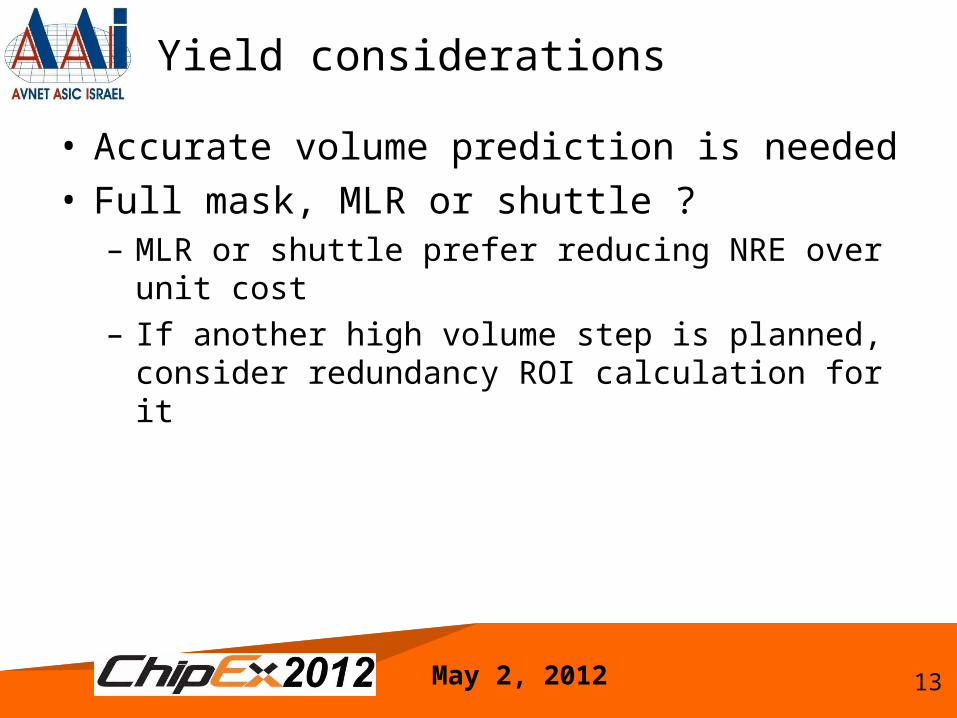
• Accurate volume prediction is needed• Full mask, MLR or shuttle ?
– MLR or shuttle prefer reducing NRE over unit cost– If another high volume step is planned, consider
redundancy ROI calculation for it
Yield considerations

May 2, 2012 14
• Basic SRAM test and repair production flow:
Production test considerations
MBISTfail
pass
redundancy config data
program config
bits
MBIST
fail
pass
continue test
programMBIST fail bin

May 2, 2012 15
• Tester time overhead is mainly due to configuration bits programming– it is only for units that fail BIST
• Tester time overhead depends on storage method and number of programmable bits– Laser Fuses – ms per die on tester + setup + seconds per
die on dedicated machine• check laser fuse machine cost
– Efuse – hundreds of ms per die on tester– OTP – tens up to hundreds ms per die on tester
Production test considerations

May 2, 2012 16
• Define SRAM list – sizes and types– SRAM size portion of total area
• Check FAB redundancy insertion guidelines – How many redundant rows and columns per SRAM ?
• Does your SRAM compiler have redundacy ?– Does it meet FAB redundancy recommendation?– Compile your SRAM list – What is area/power/timing penalty due to redundancy ?– if no, check alternative compilers cost
Design considerations - IP

May 2, 2012 17
• Hard or soft redundancy configuration ?– Does your application allow soft redundancy ?
• non automotive• BIST not sensitive to temperature or using on die
temperature sensors• prolonging reset is OK
• Soft redundancy configuration– check IP cost– check additional logic area / power / leakage– check complextity of integration to BIST– less popular today
Design considerations - IP
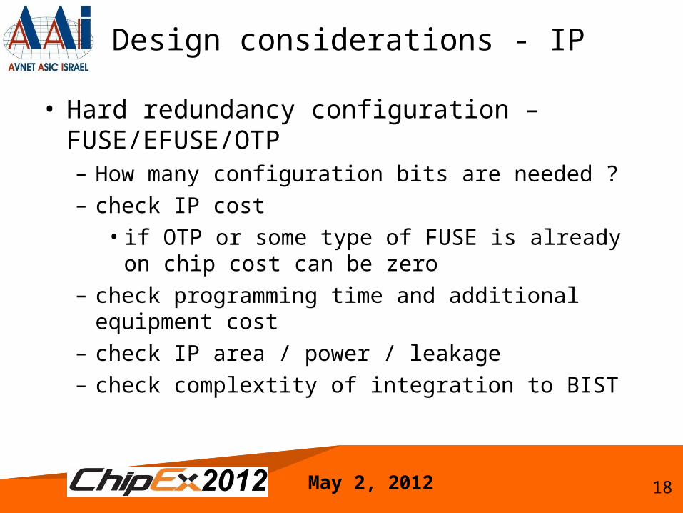
May 2, 2012 18
• Hard redundancy configuration – FUSE/EFUSE/OTP– How many configuration bits are needed ?– check IP cost
• if OTP or some type of FUSE is already on chip cost can be zero
– check programming time and additional equipment cost – check IP area / power / leakage– check complextity of integration to BIST
Design considerations - IP

May 2, 2012 19
Design considerations - BIST

May 2, 2012 20
• Does your BIST tool support redundacy ?• Does it meet FAB redundancy recommendation ?
– supports all memory types ?– supports both row and column ?
• What is area/power/timing /test time penalty due to redundancy ?– compile BIST with and without redundancy and check
overheads– how many signals per controller are added for redundancy ?
• if not supported , check alternative BIST tools cost
Design considerations - BIST

May 2, 2012 21
• Yield and Test considerations– die size, SRAM size. wafer cost– volume perdiction, full mask, MLR or shuttle ?– additional area due to redundancy insertion– repair yield– test additional cost
• Design considerations– FUSE/Efuse/OTP/ Soft repair ?– SRAM compiler, BIST, configuration IP choice and cost– Performance degradation due to redundancy: power/timing – Schedule and effort consideration
Summary – SRAM Redundancy insertion
May 2, 2012 22
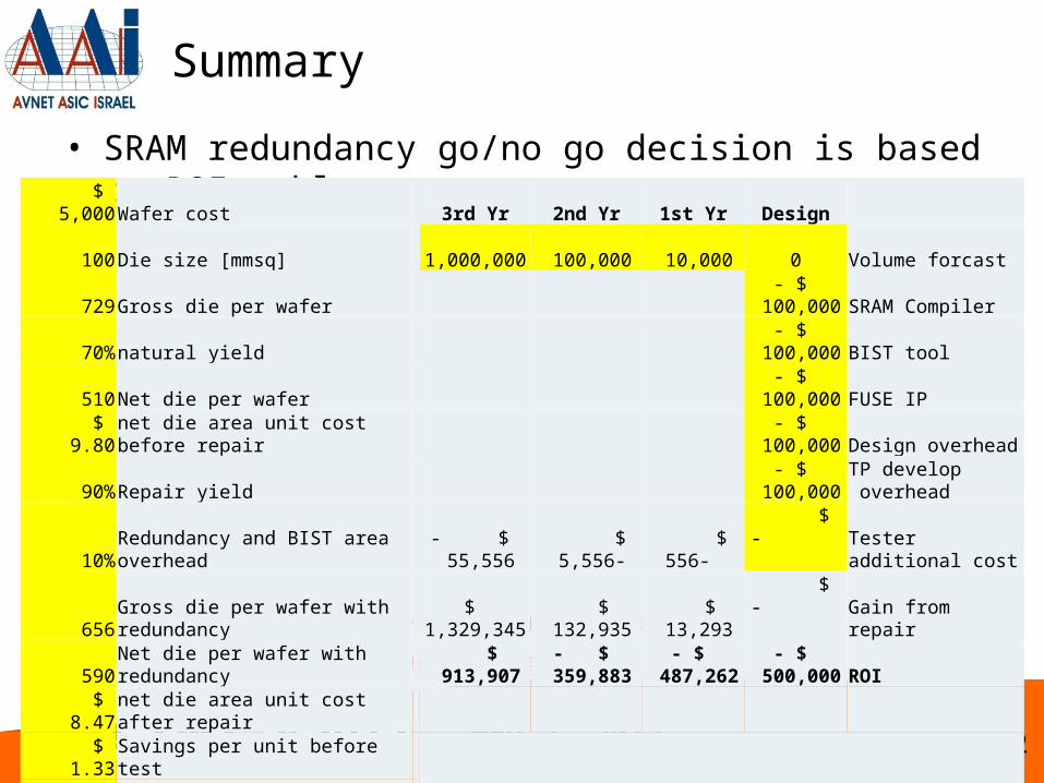
• SRAM redundancy go/no go decision is based on ROI table:
Summary
Avnet ASIC Israel LTD.
www.avnet-asic.com
Design1st Yr2nd Yr3rd YrWafer cost $ 5,000
Volume forcast0 10,000
100,000 1,000,000 Die size [mmsq]100SRAM Compiler- $ 100,000 Gross die per wafer729BIST tool- $ 100,000 natural yield70%FUSE IP- $ 100,000 Net die per wafer510Design overhead- $ 100,000 net die area unit cost before repair $ 9.80 TP develop overhead - $ 100,000 Repair yield90%
Tester additional cost - $
- $
556 - $
5,556 - $ 55,556 Redundancy and BIST area overhead10%
Gain from repair - $
$ 13,293 $
132,935 $ 1,329,345 Gross die per wafer with redundancy656
ROI- $ 500,000 - $ 487,262 - $ 359,883 $
913,907 Net die per wafer with redundancy590net die area unit cost after repair $ 8.47
All numbers mentioned are for demonstration purpose only
Savings per unit before test $ 1.33 Tester time overhead per die [sec]1Tester hour cost $ 200 Redundancy test overhead per die $ 0.06