SRA SRAMSRAMSRAM AS5C512K8 Austin Semiconductor, Inc. … · 36-Pin SOJ (DJ, ECJ & SOJ) 36-Pin CLCC...
19
SRAM AS5C512K8 AS5C512K8 Rev. 7.5 01/13 Micross Components reserves the right to change products or specifications without notice. 1 FEATURES • Ultra High Speed Asynchronous Operation • Fully Static, No Clocks • Multiple center power and ground pins for improved noise immunity • Easy memory expansion with CE\ and OE\ options • All inputs and outputs are TTL-compatible • Single +5V Power Supply +/- 10% • Data Retention Functionality Testing • Cost Efficient Plastic Packaging • Extended Testing Over -55ºC to +125ºC for plastics • Plastic 36 pin PSOJ is fully compatible with the Ceramic 36 pin SOJ and offered in lead free finish • TSOPII in Copper Lead Frame for Superior Thermal Performance 2 • RoHS Compliant Options Available OPTIONS MARKING • Timing 12ns access -12 15ns access -15 17ns access -17 20ns access -20 25ns access -25 35ns access -35 45ns access -45 • Operating Temperature Ranges Full Military (-55 o C to +125 o C) /883C Military (-55 o C to +125 o C) XT Industrial (-40 o C to +85 o C) IT • Package(s) Ceramic LCC EC Ceramic Flatpack F Plastic SOJ (Lead Free) 1 DJ Ceramic SOJ (attached formed lead) ECJ Ceramic SOJ SOJ Plastic TSOPII (44pin, 400mil) DGC 2 Plastic TSOPII (RoHS Compliant) DGCR 2 • 2V data retention/low power 3 L Notes: 1. Pb finish also available, contact factory 2. Contact factory for Copper Lead Frame Products 3. Not available for parts in DGC & DGCR packages. PIN ASSIGNMENT (Top View) AVAILABLE AS MILITARY SPECIFICATIONS •SMD 5962-95600 •SMD 5962-95613 •MIL-STD-883 512K x 8 SRAM HIGH SPEED SRAM with REVOLUTIONARY PINOUT 36-Pin SOJ (DJ, ECJ & SOJ) 36-Pin CLCC (EC) 44-Pin TSOPII (DGC & DGCR) 1 2 3 4 5 6 7 8 9 10 11 12 13 14 15 16 17 18 19 20 21 22 44 43 42 41 40 39 38 37 36 35 34 33 32 31 30 29 28 27 26 25 24 23 NC NC A0 A1 A2 A3 A4 CE I/O0 I/O1 VCC GND I/O2 I/O3 WE A5 A6 A7 A8 A9 NC NC NC NC NC A18 A17 A16 A15 OE I/O7 I/O6 GND VCC I/O5 I/O4 A14 A13 A12 A11 A10 NC NC NC 36-Pin Flat Pack (F)
Transcript of SRA SRAMSRAMSRAM AS5C512K8 Austin Semiconductor, Inc. … · 36-Pin SOJ (DJ, ECJ & SOJ) 36-Pin CLCC...
SRAMAS5C512K8
AS5C512K8Rev. 7.5 01/13
Micross Components reserves the right to change products or specifications without notice.
1
FEATURES• UltraHighSpeedAsynchronousOperation• FullyStatic,NoClocks• Multiplecenterpowerandgroundpinsforimproved noiseimmunity• EasymemoryexpansionwithCE\andOE\ options• AllinputsandoutputsareTTL-compatible• Single+5VPowerSupply+/-10%• DataRetentionFunctionalityTesting• CostEfficientPlasticPackaging• ExtendedTestingOver-55ºCto+125ºCforplastics• Plastic36pinPSOJisfullycompatiblewiththe Ceramic36pinSOJandofferedinleadfreefinish• TSOPIIinCopperLeadFrameforSuperiorThermalPerformance2• RoHSCompliantOptionsAvailable
OPTIONS MARKING• Timing 12nsaccess -12 15nsaccess -15 17nsaccess -17 20nsaccess -20 25nsaccess -25 35nsaccess -35 45nsaccess -45
• OperatingTemperatureRanges FullMilitary(-55oCto+125oC) /883C Military(-55oCto+125oC) XT Industrial(-40oCto+85oC) IT
• Package(s) CeramicLCC EC CeramicFlatpack F PlasticSOJ(LeadFree)1 DJ CeramicSOJ(attachedformedlead) ECJ CeramicSOJ SOJ PlasticTSOPII(44pin,400mil) DGC2
PlasticTSOPII(RoHSCompliant) DGCR2
• 2Vdataretention/lowpower3 LNotes:1.Pbfinishalsoavailable,contactfactory2.ContactfactoryforCopperLeadFrameProducts3.NotavailableforpartsinDGC&DGCRpackages.
PIN ASSIGNMENT (Top View)
AVAILABLE AS MILITARY SPECIFICATIONS•SMD5962-95600•SMD5962-95613•MIL-STD-883
512K x 8 SRAMHIGH SPEED SRAM withREVOLUTIONARY PINOUT
SRAMSRAMSRAMSRAMSRAMAS5C512K8
AS5C512K8Rev. 7.0 05/08
Austin Semiconductor, Inc. reserves the right to change products or specifications without notice.
1
Austin Semiconductor, Inc.
FEATURES• Ultra High Speed Asynchronous Operation• Fully Static, No Clocks• Multiple center power and ground pins for improved noise immunity• Easy memory expansion with CE\ and OE\
options• All inputs and outputs are TTL-compatible• Single +5V Power Supply +/- 10%• Data Retention Functionality Testing• Cost Efficient Plastic Packaging• Extended Testing Over -55ºC to +125ºC for plastics• Plastic 36 pin PSOJ is fully compatible with the
Ceramic 36 pin SOJ and offered in lead free finish• 3.3V Future Offering
OPTIONS MARKING• Timing
12ns access -1215ns access -1517ns access -1720ns access -2025ns access -2535ns access -3545ns access -45
• Operating Temperature RangesFull Military (-55oC to +125oC) /883CMilitary (-55oC to +125oC) XTIndustrial (-40oC to +85oC) IT
• Package(s)Ceramic LCC ECCeramic Flatpack FPlastic SOJ (Lead Free)* DJCeramic SOJ (attached formed lead) ECJCeramic SOJ SOJ* Pb finish also available, contact factory
• 2V data retention/low power L
PIN ASSIGNMENT(Top View)
36-Pin SOJ (DJ, ECJ & SOJ)36-Pin CLCC (EC)
GENERAL DESCRIPTIONThe AS5C512K8 is a high speed SRAM. It offers flexibility in
high-speed memory applications, with chip enable (CE\) and outputenable (OE\) capabilities. These features can place the outputs inHigh-Z for additional flexibility in system design.
Writing to these devices is accomplished when write enable (WE\)and CE\ inputs are both LOW. Reading is accomplished when WE\remains HIGH and CE\ and OE\ go LOW.
As a option, the device can be supplied offering a reduced powerstandby mode, allowing system designers to meet low standby powerrequirements. This device operates from a single +5V power supplyand all inputs and outputs are fully TTL-compatible.
The AS5C512K8DJ offers the convenience and reliability of theAS5C512K8 SRAM and has the cost advantage of a durable plastic.The AS5C512K8DJ is footprint compatible with 36 pin CSOJpackage of the SMD 5692-95600.
36-Pin Flat Pack (F)
AVAILABLE AS MILITARY SPECIFICATIONS•SMD 5962-95600•SMD 5962-95613•MIL-STD-883
512K x 8 SRAMHIGH SPEED SRAM withREVOLUTIONARY PINOUT
For more products and informationplease visit our web site at
www.austinsemiconductor.com
44-Pin TSOPII (DGC & DGCR)
2 Integrated Silicon Solution, Inc. — www.issi.comRev. B
03/04/2008
IS61C5128AL/AS IS64C5128AL/AS
PIN DESCRIPTIONS
A0-A18 Address Inputs
CE Chip Enable Input
OE Output Enable Input
WE Write Enable Input
I/O0-I/O7 Bidirectional Ports
VDD Power
GND Ground
NC No Connection
1
2
3
4
5
6
7
8
9
10
11
12
13
14
15
16
17
18
36
35
34
33
32
31
30
29
28
27
26
25
24
23
22
21
20
19
A0
A1
A2
A3
A4
CE
I/O0
I/O1
VDD
GND
I/O2
I/O3
WE
A5
A6
A7
A8
A9
NC
A18
A17
A16
A15
OE
I/O7
I/O6
GND
VDD
I/O5
I/O4
A14
A13
A12
A11
A10
NC
HIGH SPEED (IS61/64C5128AL) PIN CONFIGURATION
36-Pin SOJ (400-mil) 44-Pin TSOP (Type II)
12345678910111213141516171819202122
44434241403938373635343332313029282726252423
NCNCA0A1A2A3A4CE
I/O0I/O1VCCGNDI/O2I/O3WEA5A6A7A8A9NCNC
NCNCNCA18A17A16A15OEI/O7I/O6GNDVCCI/O5I/O4A14A13A12A11A10NCNCNC
SRAMSRAMSRAMSRAMSRAMAS5C512K8
AS5C512K8Rev. 7.0 05/08
Austin Semiconductor, Inc. reserves the right to change products or specifications without notice.
1
Austin Semiconductor, Inc.
FEATURES• Ultra High Speed Asynchronous Operation• Fully Static, No Clocks• Multiple center power and ground pins for improved noise immunity• Easy memory expansion with CE\ and OE\
options• All inputs and outputs are TTL-compatible• Single +5V Power Supply +/- 10%• Data Retention Functionality Testing• Cost Efficient Plastic Packaging• Extended Testing Over -55ºC to +125ºC for plastics• Plastic 36 pin PSOJ is fully compatible with the
Ceramic 36 pin SOJ and offered in lead free finish• 3.3V Future Offering
OPTIONS MARKING• Timing
12ns access -1215ns access -1517ns access -1720ns access -2025ns access -2535ns access -3545ns access -45
• Operating Temperature RangesFull Military (-55oC to +125oC) /883CMilitary (-55oC to +125oC) XTIndustrial (-40oC to +85oC) IT
• Package(s)Ceramic LCC ECCeramic Flatpack FPlastic SOJ (Lead Free)* DJCeramic SOJ (attached formed lead) ECJCeramic SOJ SOJ* Pb finish also available, contact factory
• 2V data retention/low power L
PIN ASSIGNMENT(Top View)
36-Pin SOJ (DJ, ECJ & SOJ)36-Pin CLCC (EC)
GENERAL DESCRIPTIONThe AS5C512K8 is a high speed SRAM. It offers flexibility in
high-speed memory applications, with chip enable (CE\) and outputenable (OE\) capabilities. These features can place the outputs inHigh-Z for additional flexibility in system design.
Writing to these devices is accomplished when write enable (WE\)and CE\ inputs are both LOW. Reading is accomplished when WE\remains HIGH and CE\ and OE\ go LOW.
As a option, the device can be supplied offering a reduced powerstandby mode, allowing system designers to meet low standby powerrequirements. This device operates from a single +5V power supplyand all inputs and outputs are fully TTL-compatible.
The AS5C512K8DJ offers the convenience and reliability of theAS5C512K8 SRAM and has the cost advantage of a durable plastic.The AS5C512K8DJ is footprint compatible with 36 pin CSOJpackage of the SMD 5692-95600.
36-Pin Flat Pack (F)
AVAILABLE AS MILITARY SPECIFICATIONS•SMD 5962-95600•SMD 5962-95613•MIL-STD-883
512K x 8 SRAMHIGH SPEED SRAM withREVOLUTIONARY PINOUT
For more products and informationplease visit our web site at
www.austinsemiconductor.com
SRAMAS5C512K8
AS5C512K8Rev. 7.5 01/13
Micross Components reserves the right to change products or specifications without notice.
2
SRAMSRAMSRAMSRAMSRAMAS5C512K8
AS5C512K8Rev. 7.0 05/08
Austin Semiconductor, Inc. reserves the right to change products or specifications without notice.
2
Austin Semiconductor, Inc.
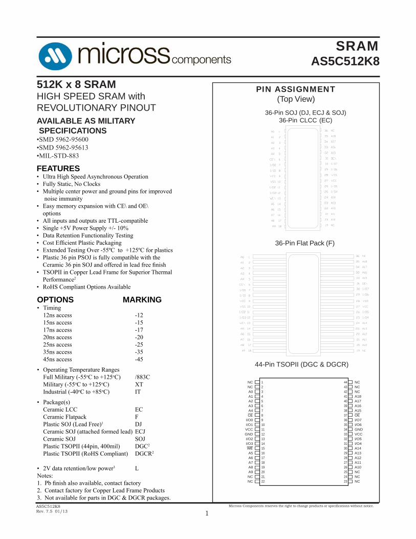
FUNCTIONAL BLOCK DIAGRAM
TRUTH TABLEMODE OE\ CE\ WE\ I/O POWERSTANDBY X H X HIGH-Z STANDBYREAD L L H Q ACTIVENOT SELECTED H L H HIGH-Z ACTIVEWRITE X L L D ACTIVE
SNOITCNUFNIP
81A-0A stupnIsserddA
\EW elbanEetirW
\EC elbanEpihC
\EO elbanEtuptuO
O/I 0 O/I- 7 stuptuO/stupnIataD
V CC rewoP
V SS dnuorG
CN noitcennoCoN
X = Don’t Care
VCC GND
INP
UT
BU
FFE
R 4,194,304-BITMEMORY ARRAY
1024 ROWS X4096 COLUMNS
I/OC
ON
TRO
LS
COLUMN DECODER
RO
W D
EC
OD
ER
*POWER DOWN
CE\
OE\
WE\
DQ8
DQ1A0-A18
*On the low voltage Data Retention option.
GENERAL DESCRIPTION TheAS5C512K8isahighspeedSRAM.Itoffersflexibilityinhigh-speedmemoryapplications,withchipenable(CE\)andoutputenable (OE\) capabilities. These features canplace theoutputs inHigh-Zforadditionalflexibilityinsystemdesign. Writingtothesedevicesisaccomplishedwhenwriteenable(WE\)andCE\inputsarebothLOW.ReadingisaccomplishedwhenWE\remainsHIGHandCE\andOE\goLOW. Asaoption,thedevicecanbesuppliedofferingareducedpower
standbymode,allowingsystemdesignerstomeetlowstandbypowerrequirements.Thisdeviceoperatesfromasingle+5VpowersupplyandallinputsandoutputsarefullyTTL-compatible. TheAS5C512K8DJofferstheconvenienceandreliabilityoftheAS5C512K8SRAMandhasthecostadvantageofadurableplastic.TheAS5C512K8DJisfootprintcompatiblewith36pinCSOJpack-ageoftheSMD5692-95600.TSOPIIwithcopperleadframeofferssuperiorthermalperformance.
SRAMAS5C512K8
AS5C512K8Rev. 7.5 01/13
Micross Components reserves the right to change products or specifications without notice.
3
ABSOLUTE MAXIMUM RATINGS*VoltageonVccSupplyRelativetoVssVcc....................................................................-.5Vto+7.0VStorageTemperature(Plastic)......................-65°Cto+150°CStorageTemperature(Ceramic)...................-55°Cto+125°CShortCircuitOutputCurrent(perI/O)…........................20mAVoltageonanyPinRelativetoVss.................-.5VtoVcc+1VMaximumJunctionTemperature**..............................+150°CPowerDissipation................................................................1W
*Stressesgreaterthanthoselistedunder“AbsoluteMaximumRatings”maycausepermanentdamagetothedevice.Thisisastressratingonlyandfunctionaloperationofthedeviceattheseoranyotherconditionsabovethoseindicatedintheoperationsectionofthisspecificationisnotimplied.Exposuretoabsolutemaximumratingconditionsforextendedperiodsmayaffectreliability.**Junctiontemperaturedependsuponpackagetype,cycletime,loading,ambienttemperatureandairflow,andhumidity.
ELECTRICAL CHARACTERISTICS AND RECOMMENDED DC OPERATING CONDITIONS (-55oC < TA < +125oC & -40oC < TA < +85oC ; Vcc = 5V +10%)
DESCRIPTION SYM -12 -15 -17 -20 -25 -35 -45 UNITS NOTES
ICCSP 100 100 100 90 90 80 70 mA 3
"L" Version Only ICCLP 75 75 75 65 65 60 50 mA
ISBTSP 20 20 20 20 20 20 20 mA
"L" Version Only ISBTLP 10 10 10 10 10 10 10 mA
ISBCSP 15 15 15 15 15 15 15 mA
"L" Version Only ISBCLP 5 5 5 5 5 5 5 mA
MAX
Power SupplyCurrent: Standby
CONDITIONSWE\=CE\<VIL; Vcc = MAX
f = MAX = 1/tRCOutputs Open
CE\ > VIH, All other inputs < VIL,Vcc = MAX, f = 0,
Outputs Open
CE\ > Vcc -0.2V; Vcc = MAXVIN<Vss +0.2V or
VIN>Vcc -0.2V; f = 0
Power SupplyCurrent: Operating
DESCRIPTION CONDITIONS SYM MIN MAX UNITS NOTESInput High (Logic 1) Voltage VIH 2.2 Vcc +0.5 V 1
Input Low (Logic 0) Voltage VIL -0.5 0.8 V 1, 2
Input Leakage Current 0V < VIN < Vcc ILI -2 2 μA
Output Leakage CurrentOutput(s) Disabled0V < VOUT < Vcc ILO
-2 2 μA
Output High Voltage IOH = -4.0 mA VOH 2.4 --- V 1
Output Low Voltage IOL = 8 mA VOL --- 0.4 V 1
Supply Voltage VCC 4.5 5.5 V 1
CAPACITANCEPARAMETER CONDITIONS SYMBOL MAX UNITS NOTES
Input Capacitance CI 8 pF 4
Output Capactiance Co 10 pF 4
TA = 25oC, f = 1MHzVIN = 0
SRAMAS5C512K8
AS5C512K8Rev. 7.5 01/13
Micross Components reserves the right to change products or specifications without notice.
4
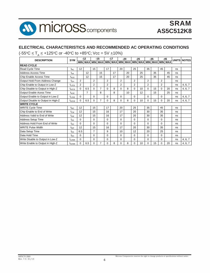
ELECTRICAL CHARACTERISTICS AND RECOMMENDED AC OPERATING CONDITIONS (-55oC < TA < +125oC or -40oC to +85oC; Vcc = 5V +10%)
MIN MAX MIN MAX MIN MAX MIN MAX MIN MAX MIN MAX MIN MAXREAD CYCLERead Cycle Time tRC 12 15 17 20 25 35 45 nsAddress Access Time tAA 12 15 17 20 25 35 45 nsChip Enable Access Time tACE 12 15 17 20 25 35 45 nsOutput Hold From Address Change tOH 2 2 2 2 2 2 2 nsChip Enable to Output in Low-Z tLZCE 2 2 2 2 2 2 2 ns 4, 6, 7 Chip Disable to Output in High-Z tHZCE 0 6.5 0 7 0 8 0 8 0 10 0 15 0 20 ns 4, 6, 7 Output Enable Acess Time tAOE 7 8 8 10 12 15 25 nsOutput Enable to Output in Low-Z tLZOE 0 0 0 0 0 0 0 ns 4, 6, 7 Output Disable to Output in High-Z tHZOE 0 6.5 0 7 0 8 0 8 0 10 0 15 0 20 ns 4, 6, 7 WRITE CYCLEWRITE Cycle Time tWC 12 15 17 20 25 35 45 nsChip Enable to End of Write tCW 12 15 16 17 20 30 35 nsAddress Valid to End of Write tAW 12 15 16 17 20 30 35 nsAddress Setup Time tAS 0 0 0 0 0 0 0 nsAddress Hold From End of Write tAH 0 0 0 0 0 0 0 nsWRITE Pulse Width tWP 12 15 16 17 20 30 35 nsData Setup Time tDS 6.5 7 9 10 12 20 25 nsData Hold Time tDH 0 0 0 0 0 0 0 nsWrite Disable to Output in Low-Z tLZWE 0 0 0 0 0 0 0 ns 4, 6, 7 Write Enable to Output in High-Z tHZWE 0 6.5 0 7 0 8 0 8 0 10 0 15 0 20 ns 4, 6, 7
-15 UNITS NOTESSYM -45-12DESCRIPTION -25-20 -35-17
SRAMAS5C512K8
AS5C512K8Rev. 7.5 01/13
Micross Components reserves the right to change products or specifications without notice.
5
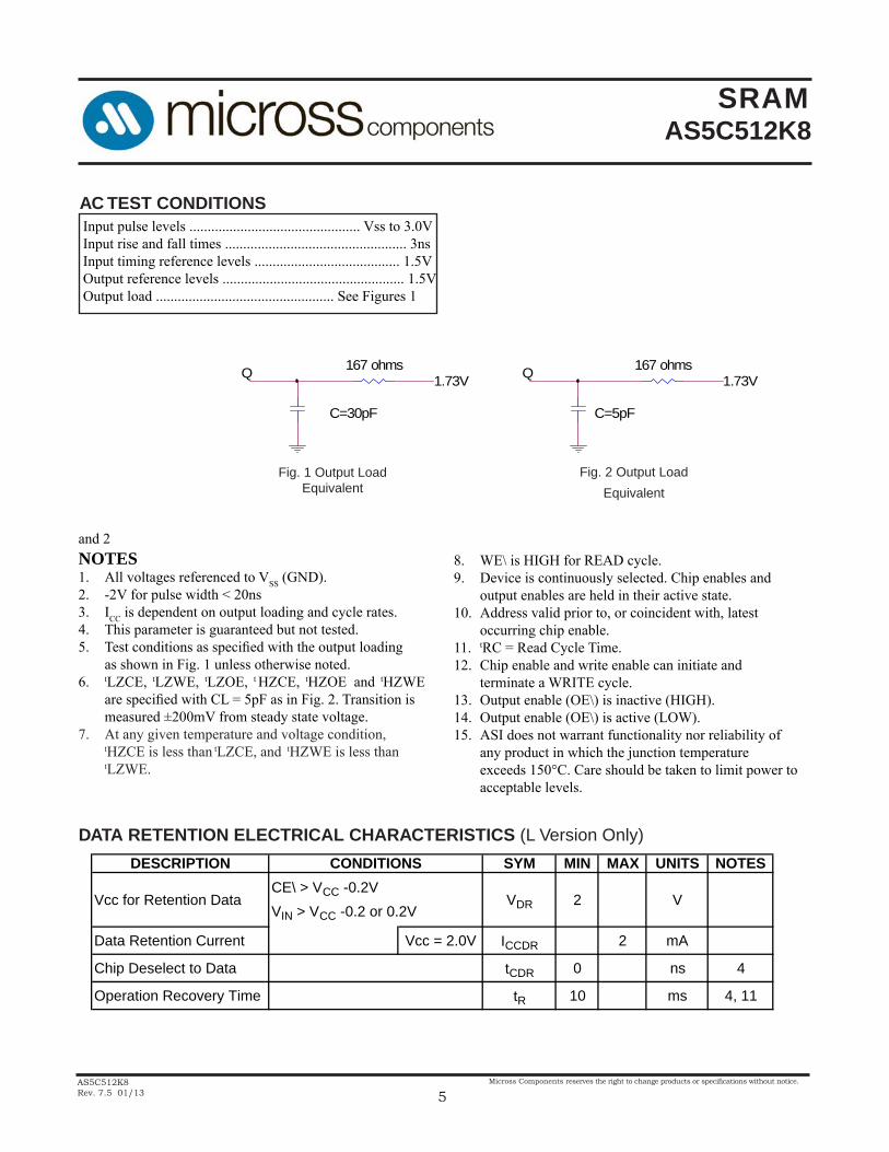
Inputpulselevels...............................................Vssto3.0VInputriseandfalltimes..................................................3nsInputtimingreferencelevels........................................1.5VOutputreferencelevels..................................................1.5VOutputload.................................................SeeFigures1
and2NOTES1. AllvoltagesreferencedtoVSS(GND).2. -2Vforpulsewidth<20ns3. ICCisdependentonoutputloadingandcyclerates.4. Thisparameterisguaranteedbutnottested.5. Testconditionsasspecifiedwiththeoutputloading asshowninFig.1unlessotherwisenoted.6. tLZCE,tLZWE,tLZOE,tHZCE,tHZOEandtHZWE arespecifiedwithCL=5pFasinFig.2.Transitionis measured±200mVfromsteadystatevoltage.7. Atanygiventemperatureandvoltagecondition, tHZCEislessthantLZCE,andtHZWEislessthan tLZWE.
8. WE\isHIGHforREADcycle.9. Deviceiscontinuouslyselected.Chipenablesand outputenablesareheldintheiractivestate.10. Addressvalidpriorto,orcoincidentwith,latest occurringchipenable.11. tRC=ReadCycleTime.12. Chipenableandwriteenablecaninitiateand terminateaWRITEcycle.13. Outputenable(OE\)isinactive(HIGH).14. Outputenable(OE\)isactive(LOW).15.ASIdoesnotwarrantfunctionalitynorreliabilityof anyproductinwhichthejunctiontemperature exceeds150°C.Careshouldbetakentolimitpowerto acceptablelevels.
Fig. 1 Output Load Equivalent
Fig. 2 Output Load Equivalent
DATA RETENTION ELECTRICAL CHARACTERISTICS (L Version Only)
AC TEST CONDITIONS
DESCRIPTION SYM MIN MAX UNITS NOTES
Vcc for Retention Data VDR 2 V
Data Retention Current Vcc = 2.0V ICCDR 2 mA
Chip Deselect to Data tCDR 0 ns 4
Operation Recovery Time tR 10 ms 4, 11
CONDITIONSCE\ > VCC -0.2VVIN > VCC -0.2 or 0.2V
SRAMSRAMSRAMSRAMSRAMAS5C512K8
AS5C512K8Rev. 7.0 05/08
Austin Semiconductor, Inc. reserves the right to change products or specifications without notice.
5
Austin Semiconductor, Inc.
167 ohms167 ohms1.73V1.73V
C=5pFC=30pF
Input pulse levels ...................................................... Vss to 3.0VInput rise and fall times ......................................................... 3nsInput timing reference levels ............................................... 1.5VOutput reference levels ........................................................ 1.5VOutput load ................................................. See Figures 1 and 2
NOTES1. All voltages referenced to V
SS (GND).
2. -2V for pulse width < 20ns3. I
CC is dependent on output loading and cycle rates.
4. This parameter is guaranteed but not tested.5. Test conditions as specified with the output loading
as shown in Fig. 1 unless otherwise noted.6. tLZCE, tLZWE, tLZOE, t HZCE, tHZOE and tHZWE
are specified with CL = 5pF as in Fig. 2. Transition ismeasured ±200mV from steady state voltage.
7. At any given temperature and voltage condition,tHZCE is less than tLZCE, and tHZWE is less thantLZWE.
8. WE\ is HIGH for READ cycle.
9. Device is continuously selected. Chip enables andoutput enables are held in their active state.
10. Address valid prior to, or coincident with, latestoccurring chip enable.
11. tRC = Read Cycle Time.12. Chip enable and write enable can initiate and
terminate a WRITE cycle.13. Output enable (OE\) is inactive (HIGH).14. Output enable (OE\) is active (LOW).15. ASI does not warrant functionality nor reliability of
any product in which the junction temperatureexceeds 150°C. Care should be taken to limit power toacceptable levels.
Fig. 1 Output LoadEquivalent
Fig. 2 Output Load
Equivalent
DATA RETENTION ELECTRICAL CHARACTERISTICS (L Version Only)
AC TEST CONDITIONS
DESCRIPTION SYM MIN MAX UNITS NOTES
Vcc for Retention Data VDR 2 V
Data Retention Current Vcc = 2.0V ICCDR 800 uA
Chip Deselect to Data tCDR 0 ns 4
Operation Recovery Time tR 10 ms 4, 11
CONDITIONS
CE\ > VCC -0.2V
VIN > VCC -0.2 or 0.2V
SRAMAS5C512K8
AS5C512K8Rev. 7.5 01/13
Micross Components reserves the right to change products or specifications without notice.
6
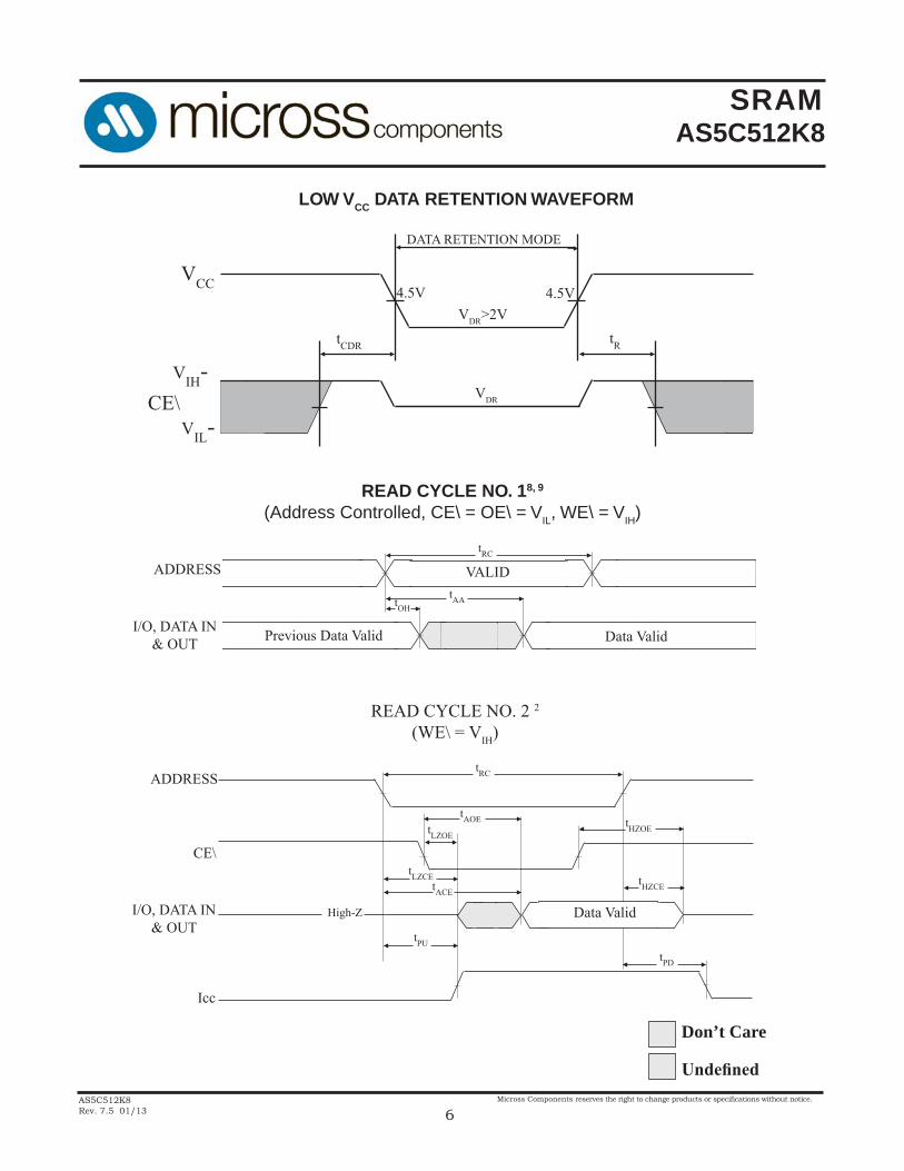
LOW VCC DATA RETENTION WAVEFORM
READ CYCLE NO. 18, 9
(Address Controlled, CE\ = OE\ = VIL, WE\ = VIH)
READCYCLENO.22(WE\=VIH)
Don’t Care
Undefined
DATARETENTIONMODE
4.5V 4.5VVDR>2V
VDR
tCDR tR
VCC
CE\VIH-
VIL-
ADDRESStRC
tOHtAA
PreviousDataValid DataValidI/O,DATAIN
&OUT
VALID
ADDRESStRC
tAOE
CE\
tLZOE
tACE
DataValidHigh-Z
tHZOE
tHZCE
tPD
I/O,DATAIN&OUT
Icc
tLZCE
tPU
SRAMAS5C512K8
AS5C512K8Rev. 7.5 01/13
Micross Components reserves the right to change products or specifications without notice.
7
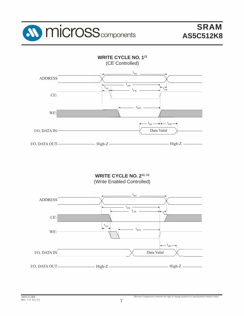
WRITE CYCLE NO. 112
(CE Controlled)
WRITE CYCLE NO. 212, 13
(Write Enabled Controlled)
ADDRESStWC
tCWCE\
tAW
DataValid
tAHtAS
I/O,DATAOUT
tWP1
tDS tDH
WE\
I/O,DATAIN
High-Z High-Z
ADDRESStWC
tCW
CE\
tAW
DataValid
tAH
tAS
I/O,DATAOUT
tWP1
tDH
WE\
I/O,DATAIN
High-Z High-Z
SRAMAS5C512K8
AS5C512K8Rev. 7.5 01/13
Micross Components reserves the right to change products or specifications without notice.
8
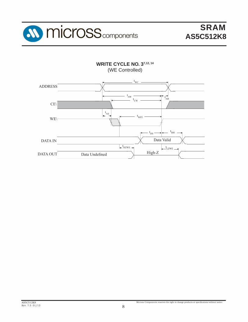
WRITE CYCLE NO. 37,12, 14
(WE Controlled)
ADDRESStWC
tCWCE\
tAW
DataValid
tAH
tAS
DATAOUT DataUndefined
tWP2
tDStDH
tHZWE tLZWE
WE\
DATAIN
High-Z
SRAMAS5C512K8
AS5C512K8Rev. 7.5 01/13
Micross Components reserves the right to change products or specifications without notice.
9
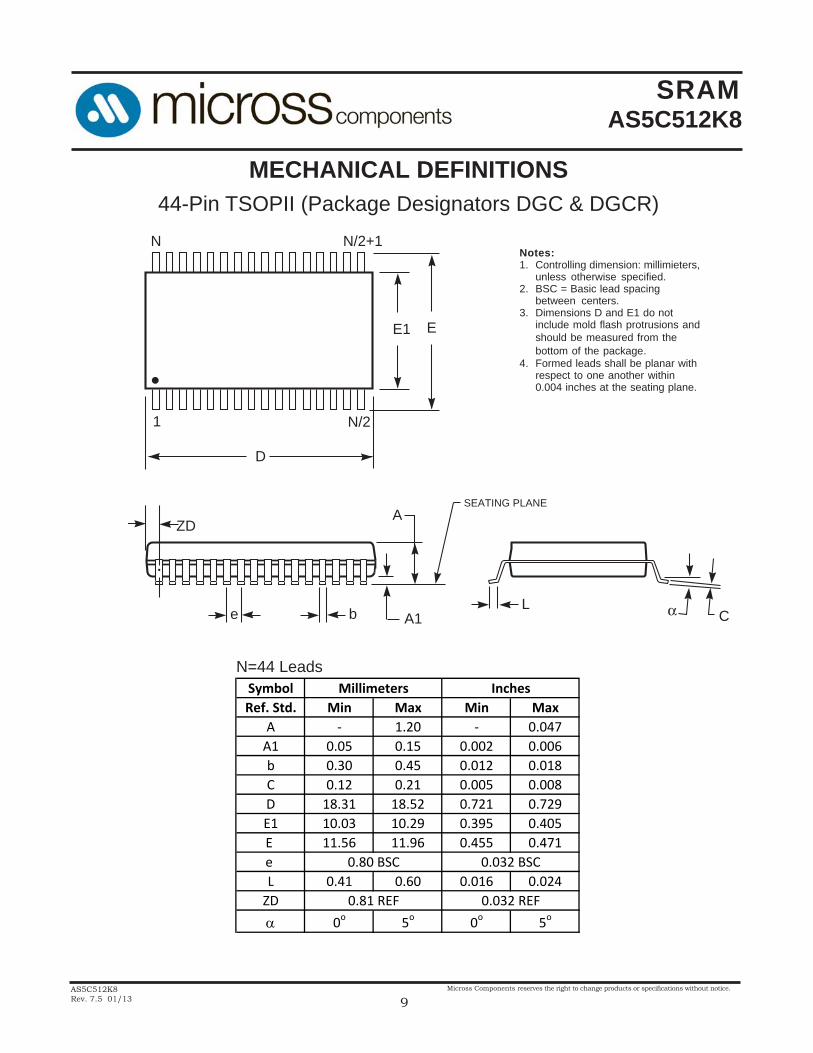
44-Pin TSOPII (Package Designators DGC & DGCR) MECHANICAL DEFINITIONS
Integrated Silicon Solution, Inc. — www.issi.com — 1-800-379-4774Rev. F06/18/03
Copyright © 2003 Integrated Silicon Solution, Inc. All rights reserved. ISSI reserves the right to make changes to this specification and its products at any timewithout notice. ISSI assumes no liability arising out of the application or use of any information, products or services described herein. Customers are advised toobtain the latest version of this device specification before relying on any published information and before placing orders for products.
PACKAGING INFORMATIONPlastic TSOPPackage Code: T (Type II)
D
SEATING PLANE
be C
1 N/2
N/2+1N
E1
A1
A
E
L α
ZD
.
Notes:1. Controlling dimension: millimieters,
unless otherwise specified.2. BSC = Basic lead spacing
between centers.3. Dimensions D and E1 do not
include mold flash protrusions andshould be measured from thebottom of the package.
4. Formed leads shall be planar withrespect to one another within0.004 inches at the seating plane.
Plastic TSOP (T - Type II)Millimeters Inches Millimeters Inches Millimeters Inches
Symbol Min Max Min Max Min Max Min Max Min Max Min MaxRef. Std.
No. Leads (N) 32 44 50A — 1.20 — 0.047 — 1.20 — 0.047 — 1.20 — 0.047A1 0.05 0.15 0.002 0.006 0.05 0.15 0.002 0.006 0.05 0.15 0.002 0.006b 0.30 0.52 0.012 0.020 0.30 0.45 0.012 0.018 0.30 0.45 0.012 0.018C 0.12 0.21 0.005 0.008 0.12 0.21 0.005 0.008 0.12 0.21 0.005 0.008D 20.82 21.08 0.820 0.830 18.31 18.52 0.721 0.729 20.82 21.08 0.820 0.830E1 10.03 10.29 0.391 0.400 10.03 10.29 0.395 0.405 10.03 10.29 0.395 0.405E 11.56 11.96 0.451 0.466 11.56 11.96 0.455 0.471 11.56 11.96 0.455 0.471e 1.27 BSC 0.050 BSC 0.80 BSC 0.032 BSC 0.80 BSC 0.031 BSCL 0.40 0.60 0.016 0.024 0.41 0.60 0.016 0.024 0.40 0.60 0.016 0.024
ZD 0.95 REF 0.037 REF 0.81 REF 0.032 REF 0.88 REF 0.035 REFα 0° 5° 0° 5° 0° 5° 0° 5° 0° 5° 0° 5°
SymbolRef. Std. Min Max Min Max
A ‐ 1.20 ‐ 0.047A1 0.05 0.15 0.002 0.006b 0.30 0.45 0.012 0.018C 0.12 0.21 0.005 0.008D 18.31 18.52 0.721 0.729E1 10.03 10.29 0.395 0.405E 11.56 11.96 0.455 0.471e L 0.41 0.60 0.016 0.024ZD
α 0o 5o 0o 5o
Millimeters Inches
0.81 REF
0.80 BSC 0.032 BSC
0.032 REF
N=44 Leads
SRAMAS5C512K8
AS5C512K8Rev. 7.5 01/13
Micross Components reserves the right to change products or specifications without notice.
10
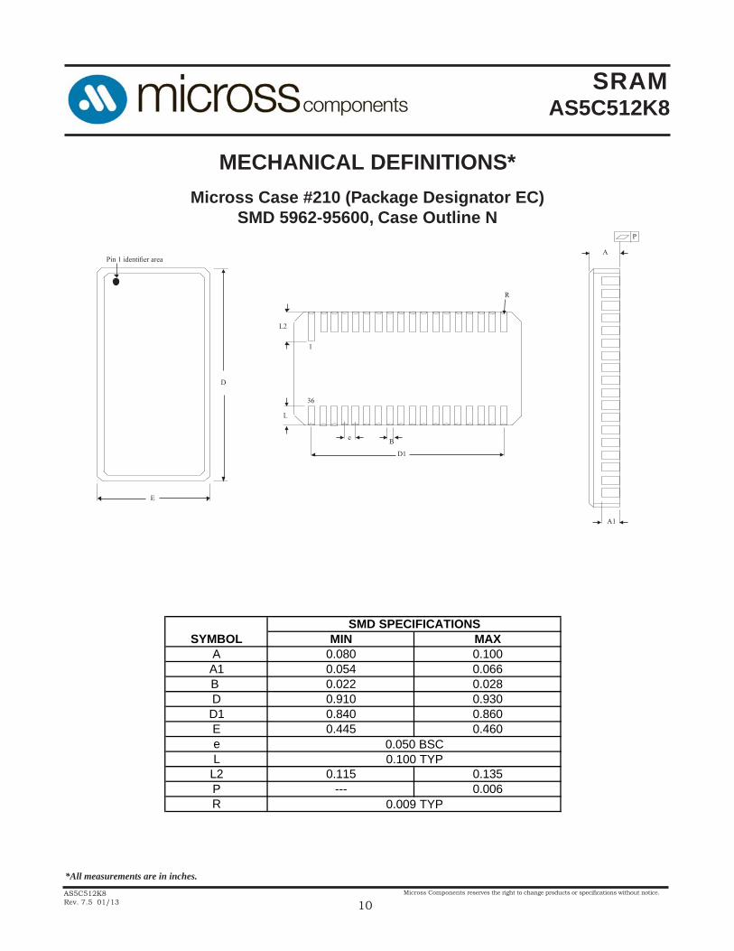
MECHANICAL DEFINITIONS*
Micross Case #210 (Package Designator EC)SMD 5962-95600, Case Outline N
D
E
Pin1identifierarea
L2
L
e B
R
D1
1
36
*All measurements are in inches.
A
A1
P
SRAMSRAMSRAMSRAMSRAMAS5C512K8
AS5C512K8Rev. 7.0 05/08
Austin Semiconductor, Inc. reserves the right to change products or specifications without notice.
9
Austin Semiconductor, Inc.
MECHANICAL DEFINITIONS*
ASI Case #210 (Package Designator EC)SMD 5962-95600, Case Outline N
D
E
Pin 1 identifier area
L2
L
eB
R
D1
1
36
MIN MAXA 0.080 0.100A1 0.054 0.066B 0.022 0.028D 0.910 0.930D1 0.840 0.860E 0.445 0.460eL
L2 0.115 0.135P --- 0.006R 0.009 TYP
SYMBOL
0.100 TYP
SMD SPECIFICATIONS
0.050 BSC
*All measurements are in inches.
A
A1
P
SRAMAS5C512K8
AS5C512K8Rev. 7.5 01/13
Micross Components reserves the right to change products or specifications without notice.
11
MECHANICAL DEFINITIONS*
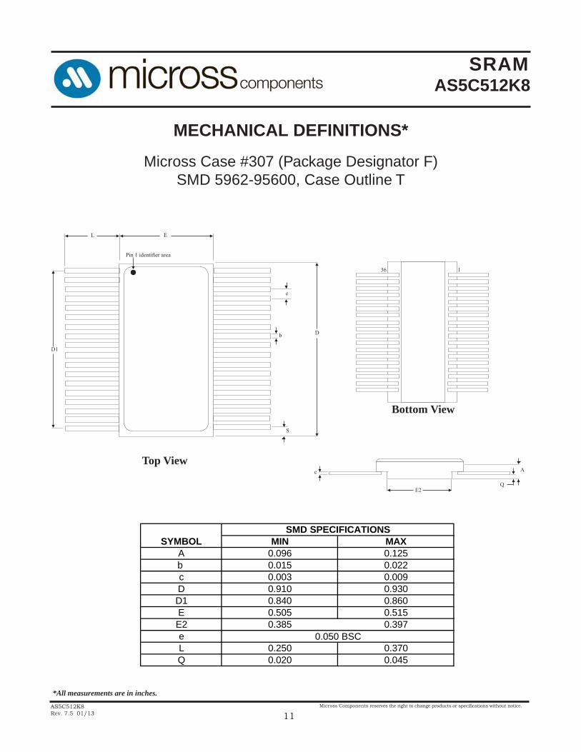
Micross Case #307 (Package Designator F)SMD 5962-95600, Case Outline T
Bottom View
36 1
c
E2
A
Q
*All measurements are in inches.
D
e
b
Top View
D1
S
EL
Pin1identifierarea
SRAMSRAMSRAMSRAMSRAMAS5C512K8
AS5C512K8Rev. 7.0 05/08
Austin Semiconductor, Inc. reserves the right to change products or specifications without notice.
10
Austin Semiconductor, Inc.
MECHANICAL DEFINITIONS*
ASI Case #307 (Package Designator F)SMD 5962-95600, Case Outline T
Bottom View
36 1
c
E2
A
Q
MIN MAXA 0.096 0.125b 0.015 0.022c 0.003 0.009D 0.910 0.930D1 0.840 0.860E 0.505 0.515E2 0.385 0.397eL 0.250 0.370Q 0.020 0.045
SYMBOL
0.050 BSC
SMD SPECIFICATIONS
*All measurements are in inches.
D
e
b
Top View
D1
S
EL
Pin 1 identifier area
SRAMAS5C512K8
AS5C512K8Rev. 7.5 01/13
Micross Components reserves the right to change products or specifications without notice.
12
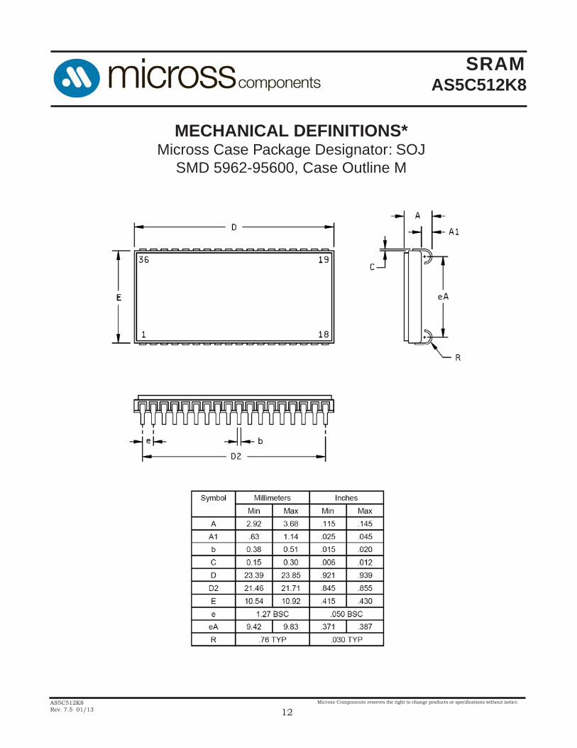
MECHANICAL DEFINITIONS*Micross Case Package Designator: SOJ
SMD 5962-95600, Case Outline M
SRAMAS5C512K8
AS5C512K8Rev. 7.5 01/13
Micross Components reserves the right to change products or specifications without notice.
13
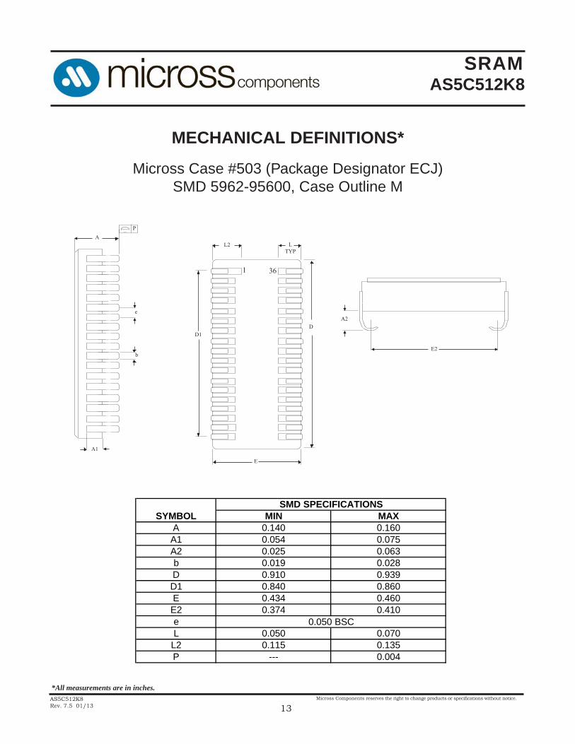
MECHANICAL DEFINITIONS*
Micross Case #503 (Package Designator ECJ)SMD 5962-95600, Case Outline M
*All measurements are in inches.
A
A1
e
b
P
A2
E2
D
E
D1
L2 LTYP
1 36
SRAMSRAMSRAMSRAMSRAMAS5C512K8
AS5C512K8Rev. 7.0 05/08
Austin Semiconductor, Inc. reserves the right to change products or specifications without notice.
12
Austin Semiconductor, Inc.
MECHANICAL DEFINITIONS*
ASI Case #503 (Package Designator ECJ)SMD 5962-95600, Case Outline M
*All measurements are in inches.
A
A1
e
b
P
A2
E2
MIN MAXA 0.140 0.160A1 0.054 0.075A2 0.025 0.063b 0.019 0.028D 0.910 0.939D1 0.840 0.860E 0.434 0.460E2 0.374 0.410eL 0.050 0.070
L2 0.115 0.135P --- 0.004
SYMBOLSMD SPECIFICATIONS
0.050 BSC
D
E
D1
L2 LTYP
1 36
SRAMAS5C512K8
AS5C512K8Rev. 7.5 01/13
Micross Components reserves the right to change products or specifications without notice.
14
*All measurements are in inches.
MECHANICAL DEFINITIONS*
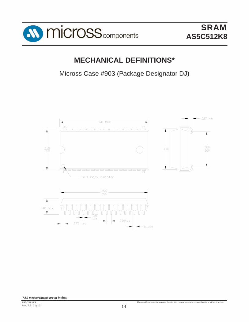
Micross Case #903 (Package Designator DJ)
SRAMSRAMSRAMSRAMSRAMAS5C512K8
AS5C512K8Rev. 7.0 05/08
Austin Semiconductor, Inc. reserves the right to change products or specifications without notice.
13
Austin Semiconductor, Inc.
*All measurements are in inches.
MECHANICAL DEFINITIONS*
ASI Case #903 (Package Designator DJ)
SRAMAS5C512K8
AS5C512K8Rev. 7.5 01/13
Micross Components reserves the right to change products or specifications without notice.
15
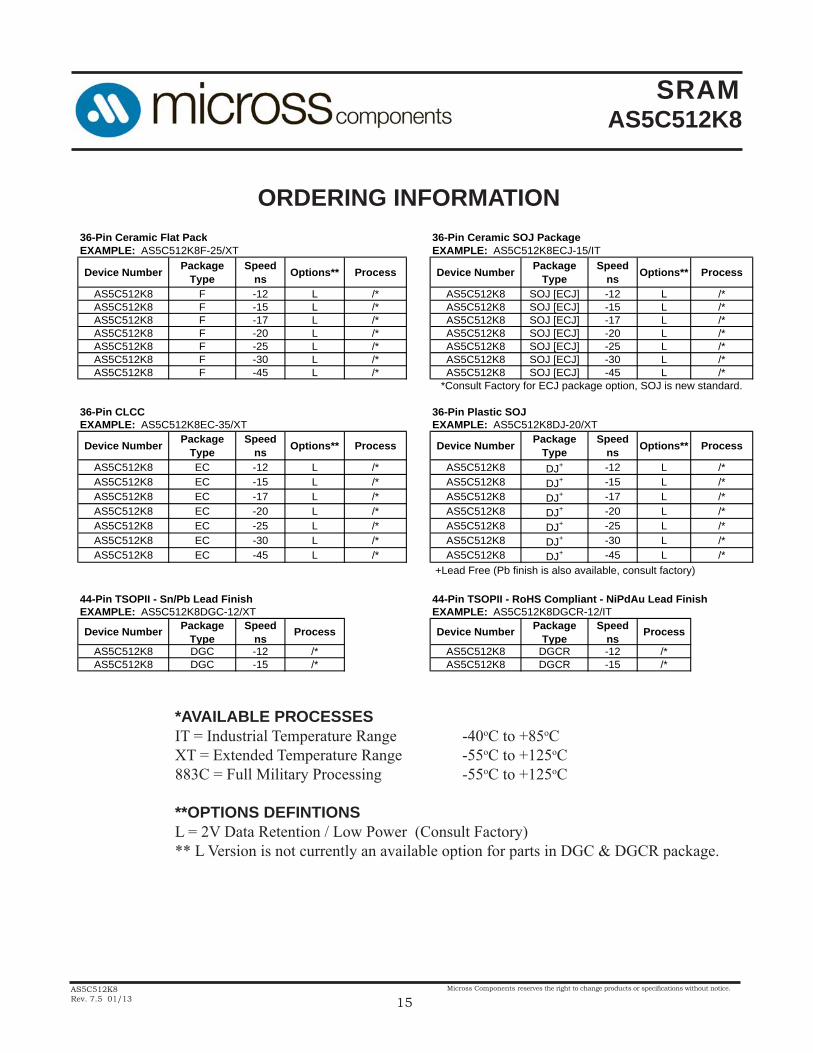
ORDERING INFORMATION
*AVAILABLE PROCESSESIT=IndustrialTemperatureRange -40oCto+85oCXT=ExtendedTemperatureRange -55oCto+125oC883C=FullMilitaryProcessing -55oCto+125oC
**OPTIONS DEFINTIONSL=2VDataRetention/LowPower(ConsultFactory)**LVersionisnotcurrentlyanavailableoptionforpartsinDGC&DGCRpackage.
36-Pin Ceramic Flat Pack 36-Pin Ceramic SOJ Package
Device Number PackageType
Speedns Options** Process Device Number Package
TypeSpeed
ns Options** Process
AS5C512K8 F -12 L /* AS5C512K8 SOJ [ECJ] -12 L /*AS5C512K8 F -15 L /* AS5C512K8 SOJ [ECJ] -15 L /*AS5C512K8 F -17 L /* AS5C512K8 SOJ [ECJ] -17 L /*AS5C512K8 F -20 L /* AS5C512K8 SOJ [ECJ] -20 L /*AS5C512K8 F -25 L /* AS5C512K8 SOJ [ECJ] -25 L /*AS5C512K8 F -30 L /* AS5C512K8 SOJ [ECJ] -30 L /*AS5C512K8 F -45 L /* AS5C512K8 SOJ [ECJ] -45 L /*
36-Pin CLCC 36-Pin Plastic SOJ
Device Number PackageType
Speedns Options** Process Device Number Package
TypeSpeed
ns Options** Process
AS5C512K8 EC -12 L /* AS5C512K8 DJ+ -12 L /*AS5C512K8 EC -15 L /* AS5C512K8 DJ+ -15 L /*AS5C512K8 EC -17 L /* AS5C512K8 DJ+ -17 L /*AS5C512K8 EC -20 L /* AS5C512K8 DJ+ -20 L /*AS5C512K8 EC -25 L /* AS5C512K8 DJ+ -25 L /*AS5C512K8 EC -30 L /* AS5C512K8 DJ+ -30 L /*AS5C512K8 EC -45 L /* AS5C512K8 DJ+ -45 L /*
44-Pin TSOPII - Sn/Pb Lead Finish 44-Pin TSOPII - RoHS Compliant - NiPdAu Lead Finish
Device Number PackageType
Speedns
Process Device Number PackageType
Speedns
Process
AS5C512K8 DGC -12 /* AS5C512K8 DGCR -12 /*AS5C512K8 DGC -15 /* AS5C512K8 DGCR -15 /*
EXAMPLE: AS5C512K8DGC-12/XT EXAMPLE: AS5C512K8DGCR-12/IT
+Lead Free (Pb finish is also available, consult factory)
EXAMPLE: AS5C512K8F-25/XT
EXAMPLE: AS5C512K8EC-35/XT
EXAMPLE: AS5C512K8ECJ-15/IT
EXAMPLE: AS5C512K8DJ-20/XT
*Consult Factory for ECJ package option, SOJ is new standard.
SRAMAS5C512K8
AS5C512K8Rev. 7.5 01/13
Micross Components reserves the right to change products or specifications without notice.
16
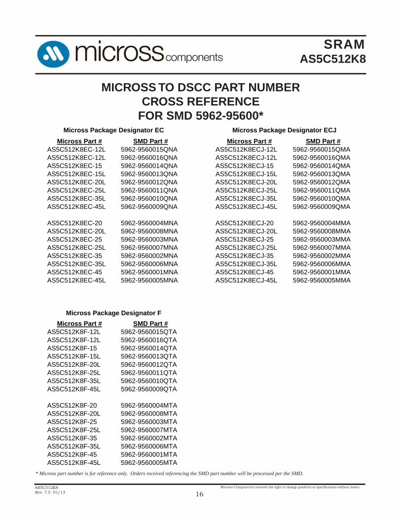
MICROSS TO DSCC PART NUMBER CROSS REFERENCE
FOR SMD 5962-95600*
* Micross part number is for reference only. Orders received referencing the SMD part number will be processed per the SMD.
Micross Part # SMD Part # Micross Part # SMD Part #AS5C512K8EC-12L 5962-9560015QNA AS5C512K8ECJ-12L 5962-9560015QMAAS5C512K8EC-12L 5962-9560016QNA AS5C512K8ECJ-12L 5962-9560016QMAAS5C512K8EC-15 5962-9560014QNA AS5C512K8ECJ-15 5962-9560014QMAAS5C512K8EC-15L 5962-9560013QNA AS5C512K8ECJ-15L 5962-9560013QMAAS5C512K8EC-20L 5962-9560012QNA AS5C512K8ECJ-20L 5962-9560012QMAAS5C512K8EC-25L 5962-9560011QNA AS5C512K8ECJ-25L 5962-9560011QMAAS5C512K8EC-35L 5962-9560010QNA AS5C512K8ECJ-35L 5962-9560010QMAAS5C512K8EC-45L 5962-9560009QNA AS5C512K8ECJ-45L 5962-9560009QMA
AS5C512K8EC-20 5962-9560004MNA AS5C512K8ECJ-20 5962-9560004MMAAS5C512K8EC-20L 5962-9560008MNA AS5C512K8ECJ-20L 5962-9560008MMAAS5C512K8EC-25 5962-9560003MNA AS5C512K8ECJ-25 5962-9560003MMAAS5C512K8EC-25L 5962-9560007MNA AS5C512K8ECJ-25L 5962-9560007MMAAS5C512K8EC-35 5962-9560002MNA AS5C512K8ECJ-35 5962-9560002MMAAS5C512K8EC-35L 5962-9560006MNA AS5C512K8ECJ-35L 5962-9560006MMAAS5C512K8EC-45 5962-9560001MNA AS5C512K8ECJ-45 5962-9560001MMAAS5C512K8EC-45L 5962-9560005MNA AS5C512K8ECJ-45L 5962-9560005MMA
Micross Part # SMD Part #AS5C512K8F-12L 5962-9560015QTAAS5C512K8F-12L 5962-9560016QTAAS5C512K8F-15 5962-9560014QTAAS5C512K8F-15L 5962-9560013QTAAS5C512K8F-20L 5962-9560012QTAAS5C512K8F-25L 5962-9560011QTAAS5C512K8F-35L 5962-9560010QTAAS5C512K8F-45L 5962-9560009QTA
AS5C512K8F-20 5962-9560004MTAAS5C512K8F-20L 5962-9560008MTAAS5C512K8F-25 5962-9560003MTAAS5C512K8F-25L 5962-9560007MTAAS5C512K8F-35 5962-9560002MTAAS5C512K8F-35L 5962-9560006MTAAS5C512K8F-45 5962-9560001MTAAS5C512K8F-45L 5962-9560005MTA
Micross Package Designator EC Micross Package Designator ECJ
Micross Package Designator F
SRAMAS5C512K8
AS5C512K8Rev. 7.5 01/13
Micross Components reserves the right to change products or specifications without notice.
17
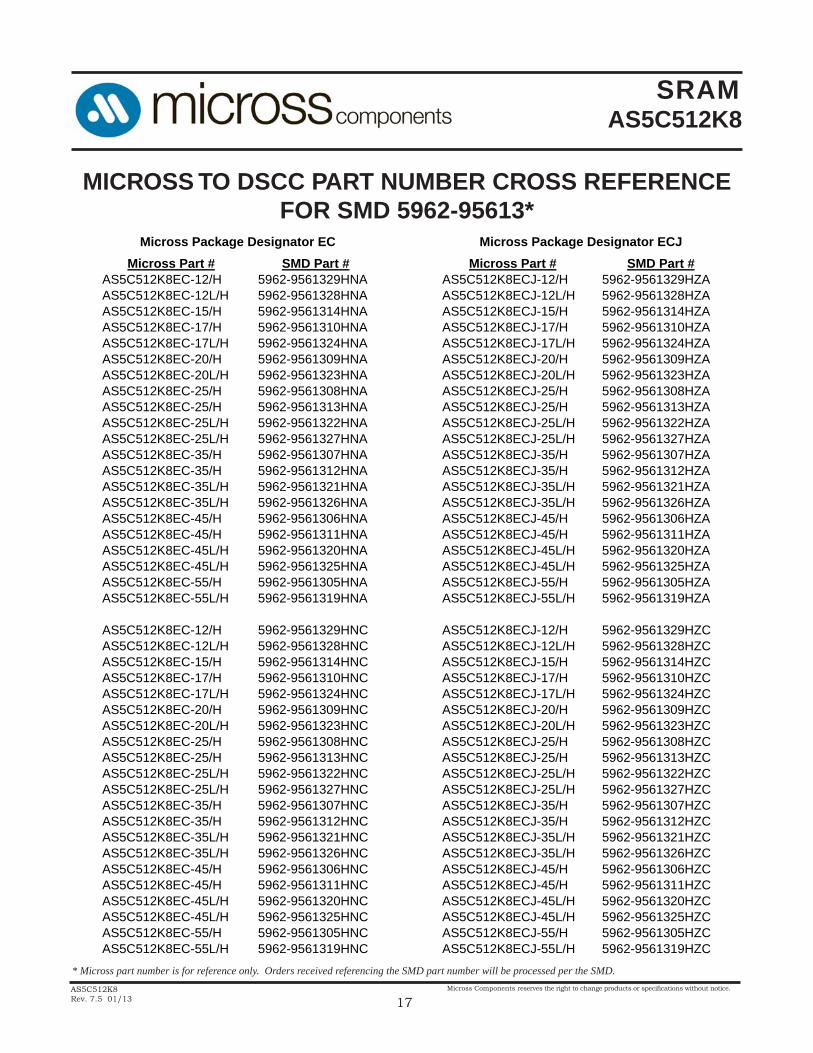
MICROSS TO DSCC PART NUMBER CROSS REFERENCEFOR SMD 5962-95613*
* Micross part number is for reference only. Orders received referencing the SMD part number will be processed per the SMD.
Micross Part # SMD Part # Micross Part # SMD Part #AS5C512K8EC-12/H 5962-9561329HNA AS5C512K8ECJ-12/H 5962-9561329HZAAS5C512K8EC-12L/H 5962-9561328HNA AS5C512K8ECJ-12L/H 5962-9561328HZAAS5C512K8EC-15/H 5962-9561314HNA AS5C512K8ECJ-15/H 5962-9561314HZAAS5C512K8EC-17/H 5962-9561310HNA AS5C512K8ECJ-17/H 5962-9561310HZAAS5C512K8EC-17L/H 5962-9561324HNA AS5C512K8ECJ-17L/H 5962-9561324HZAAS5C512K8EC-20/H 5962-9561309HNA AS5C512K8ECJ-20/H 5962-9561309HZAAS5C512K8EC-20L/H 5962-9561323HNA AS5C512K8ECJ-20L/H 5962-9561323HZAAS5C512K8EC-25/H 5962-9561308HNA AS5C512K8ECJ-25/H 5962-9561308HZAAS5C512K8EC-25/H 5962-9561313HNA AS5C512K8ECJ-25/H 5962-9561313HZAAS5C512K8EC-25L/H 5962-9561322HNA AS5C512K8ECJ-25L/H 5962-9561322HZAAS5C512K8EC-25L/H 5962-9561327HNA AS5C512K8ECJ-25L/H 5962-9561327HZAAS5C512K8EC-35/H 5962-9561307HNA AS5C512K8ECJ-35/H 5962-9561307HZAAS5C512K8EC-35/H 5962-9561312HNA AS5C512K8ECJ-35/H 5962-9561312HZAAS5C512K8EC-35L/H 5962-9561321HNA AS5C512K8ECJ-35L/H 5962-9561321HZAAS5C512K8EC-35L/H 5962-9561326HNA AS5C512K8ECJ-35L/H 5962-9561326HZAAS5C512K8EC-45/H 5962-9561306HNA AS5C512K8ECJ-45/H 5962-9561306HZAAS5C512K8EC-45/H 5962-9561311HNA AS5C512K8ECJ-45/H 5962-9561311HZAAS5C512K8EC-45L/H 5962-9561320HNA AS5C512K8ECJ-45L/H 5962-9561320HZAAS5C512K8EC-45L/H 5962-9561325HNA AS5C512K8ECJ-45L/H 5962-9561325HZAAS5C512K8EC-55/H 5962-9561305HNA AS5C512K8ECJ-55/H 5962-9561305HZAAS5C512K8EC-55L/H 5962-9561319HNA AS5C512K8ECJ-55L/H 5962-9561319HZA
AS5C512K8EC-12/H 5962-9561329HNC AS5C512K8ECJ-12/H 5962-9561329HZCAS5C512K8EC-12L/H 5962-9561328HNC AS5C512K8ECJ-12L/H 5962-9561328HZCAS5C512K8EC-15/H 5962-9561314HNC AS5C512K8ECJ-15/H 5962-9561314HZCAS5C512K8EC-17/H 5962-9561310HNC AS5C512K8ECJ-17/H 5962-9561310HZCAS5C512K8EC-17L/H 5962-9561324HNC AS5C512K8ECJ-17L/H 5962-9561324HZCAS5C512K8EC-20/H 5962-9561309HNC AS5C512K8ECJ-20/H 5962-9561309HZCAS5C512K8EC-20L/H 5962-9561323HNC AS5C512K8ECJ-20L/H 5962-9561323HZCAS5C512K8EC-25/H 5962-9561308HNC AS5C512K8ECJ-25/H 5962-9561308HZCAS5C512K8EC-25/H 5962-9561313HNC AS5C512K8ECJ-25/H 5962-9561313HZCAS5C512K8EC-25L/H 5962-9561322HNC AS5C512K8ECJ-25L/H 5962-9561322HZCAS5C512K8EC-25L/H 5962-9561327HNC AS5C512K8ECJ-25L/H 5962-9561327HZCAS5C512K8EC-35/H 5962-9561307HNC AS5C512K8ECJ-35/H 5962-9561307HZCAS5C512K8EC-35/H 5962-9561312HNC AS5C512K8ECJ-35/H 5962-9561312HZCAS5C512K8EC-35L/H 5962-9561321HNC AS5C512K8ECJ-35L/H 5962-9561321HZCAS5C512K8EC-35L/H 5962-9561326HNC AS5C512K8ECJ-35L/H 5962-9561326HZCAS5C512K8EC-45/H 5962-9561306HNC AS5C512K8ECJ-45/H 5962-9561306HZCAS5C512K8EC-45/H 5962-9561311HNC AS5C512K8ECJ-45/H 5962-9561311HZCAS5C512K8EC-45L/H 5962-9561320HNC AS5C512K8ECJ-45L/H 5962-9561320HZCAS5C512K8EC-45L/H 5962-9561325HNC AS5C512K8ECJ-45L/H 5962-9561325HZCAS5C512K8EC-55/H 5962-9561305HNC AS5C512K8ECJ-55/H 5962-9561305HZCAS5C512K8EC-55L/H 5962-9561319HNC AS5C512K8ECJ-55L/H 5962-9561319HZC
Micross Package Designator EC Micross Package Designator ECJ
SRAMAS5C512K8
AS5C512K8Rev. 7.5 01/13
Micross Components reserves the right to change products or specifications without notice.
18
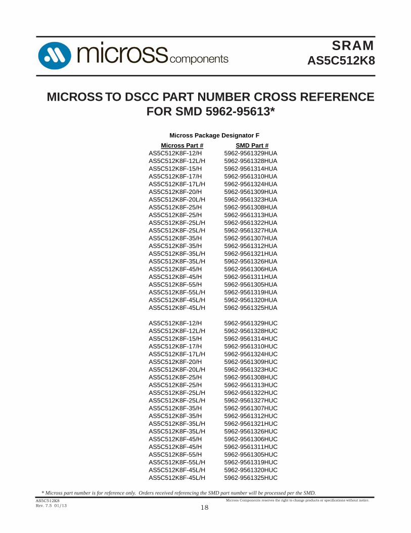
MICROSS TO DSCC PART NUMBER CROSS REFERENCEFOR SMD 5962-95613*
* Micross part number is for reference only. Orders received referencing the SMD part number will be processed per the SMD.
Micross Part # SMD Part #AS5C512K8F-12/H 5962-9561329HUAAS5C512K8F-12L/H 5962-9561328HUAAS5C512K8F-15/H 5962-9561314HUAAS5C512K8F-17/H 5962-9561310HUAAS5C512K8F-17L/H 5962-9561324HUAAS5C512K8F-20/H 5962-9561309HUAAS5C512K8F-20L/H 5962-9561323HUAAS5C512K8F-25/H 5962-9561308HUAAS5C512K8F-25/H 5962-9561313HUAAS5C512K8F-25L/H 5962-9561322HUAAS5C512K8F-25L/H 5962-9561327HUAAS5C512K8F-35/H 5962-9561307HUAAS5C512K8F-35/H 5962-9561312HUAAS5C512K8F-35L/H 5962-9561321HUAAS5C512K8F-35L/H 5962-9561326HUAAS5C512K8F-45/H 5962-9561306HUAAS5C512K8F-45/H 5962-9561311HUAAS5C512K8F-55/H 5962-9561305HUAAS5C512K8F-55L/H 5962-9561319HUAAS5C512K8F-45L/H 5962-9561320HUAAS5C512K8F-45L/H 5962-9561325HUA
AS5C512K8F-12/H 5962-9561329HUCAS5C512K8F-12L/H 5962-9561328HUCAS5C512K8F-15/H 5962-9561314HUCAS5C512K8F-17/H 5962-9561310HUCAS5C512K8F-17L/H 5962-9561324HUCAS5C512K8F-20/H 5962-9561309HUCAS5C512K8F-20L/H 5962-9561323HUCAS5C512K8F-25/H 5962-9561308HUCAS5C512K8F-25/H 5962-9561313HUCAS5C512K8F-25L/H 5962-9561322HUCAS5C512K8F-25L/H 5962-9561327HUCAS5C512K8F-35/H 5962-9561307HUCAS5C512K8F-35/H 5962-9561312HUCAS5C512K8F-35L/H 5962-9561321HUCAS5C512K8F-35L/H 5962-9561326HUCAS5C512K8F-45/H 5962-9561306HUCAS5C512K8F-45/H 5962-9561311HUCAS5C512K8F-55/H 5962-9561305HUCAS5C512K8F-55L/H 5962-9561319HUCAS5C512K8F-45L/H 5962-9561320HUCAS5C512K8F-45L/H 5962-9561325HUC
Micross Package Designator F
SRAMAS5C512K8
AS5C512K8Rev. 7.5 01/13
Micross Components reserves the right to change products or specifications without notice.
19
DOCUMENT TITLE512K x 8 SRAM HIGH SPEED SRAM with REVOLUTIONARY PINOUT
REVISION HISTORYRev # History Release Date Status7.1 Updated 36 lead SOJ Drawing September 2008 Release
7.2 Added Micross Information January 2010 Release
7.3 Expanded package offering to include March 2011 Release Copper Lead Frames and RoHS compliancy, pages 1&14, changed elect. char. limits: From: To: ICCSP 225mA for all speeds 100mA for -12,-15 & -17 90mA for -20 & -25 80mA for -35 70mA for -45 ICCLP 180mA for all speeds 75mA for -12,-15 & -17 65mA for -20 & -25 60mA for -35 50mA for -45 ISBTSP 60mA for all speeds 20mA for all speeds ISBTLP 30mA for all speeds 10mA for all speeds ISBCSP 25mA for all speeds 15mA for all speeds ISBCLP 10mA for all speeds 5mA for all speeds ILI ±10µA ±2µA CI 12pF 8pF CO 14pF 10pF tAH 1ns for all speeds 0ns for all speeds tHZWE 25ns -35 & 30ns -45 15ns -35 & 20ns -45
7.4 Updated Data Retention Electrical August 2012 Release Characteristics (L Version Only) ICCDR max. from 800 uA to 4.5 mA
7.5 Updated Data Retention Electrical January 2013 Release Characteristics (L Version Only) ICCDR max. from 4.5mA to 2mA

![) SOJ. C-l h^ Are Lbyy] upg/ l iftcitw stateFILE/0001171C.pdf · 2020-05-11 · V i \) SOJ. C-l h^ Are Parish Lbyy] upg/ l iftcitw state J 0 ENTITY NAME ANNUAL SWORN FINANCIAL STATEMENTS](https://static.fdocuments.in/doc/165x107/5edcd81ead6a402d6667b19d/-soj-c-l-h-are-lbyy-upg-l-iftcitw-state-file-2020-05-11-v-i-soj-c-l.jpg)


![RepoRt - Olijf_netwerk_vrouwen...Improving the treatment of rare gynaecological cancers Isabelle Ray Coquard (Centre Léon Bérard, Centre de Lutte Contre le Cancer [CLCC], France)](https://static.fdocuments.in/doc/165x107/5f59781d80fc07785b232284/report-olijf-netwerkvrouwen-improving-the-treatment-of-rare-gynaecological.jpg)