
Spin Tronic s
175
THIN FILM OXIDES AND HETEROSTRUCTURES FOR SPINTRONICS Sourav Chattopadhyay
-
Upload
sundeep-seesala -
Category
Documents
-
view
36 -
download
2
description
phd thesis on zno thin film magnetism
Transcript of Spin Tronic s

THIN FILM OXIDES AND HETEROSTRUCTURES FOR
SPINTRONICS
Sourav Chattopadhyay

i
THIN FILM OXIDES AND HETEROSTRUCTURES FOR
SPINTRONICS
Thesis submitted to the
Indian Institute of Technology, Kharagpur
For award of the degree
of
Doctor of Philosophy
by Sourav Chattopadhyay
Under the guidance of
Dr. T. K. Nath
& Dr. P. Banerji
DEPARTMENT OF PHYSICS AND METEOROLOGY
INDIAN INSTITUTE OF TECHNOLOGY KHARAGPUR
MAY 2011 © 2011 Sourav Chattopadhyay. All rights reserved.

ii
APPROVAL OF THE VIVA-VOCE BOARD
Certified that the thesis entitled THIN FILM OXIDES AND HETEROSTRUCTURES FOR
SPINTRONICS submitted by SOURAV CHATTOAPDHYAY to the Indian Institute of
Technology, Kharagpur, for the award of the degree Doctor of Philosophy has been accepted by
the external examiners and that the student has successfully defended the thesis in the viva-voce
examination held today.
(Member of the DSC) (Member of the DSC) (Member of the DSC) (Supervisor) (Supervisor) (External Examiner) (Chairman)

iii
CERTIFICATE
This is to certify that the thesis entitled “Thin film oxides and heterostructures for
spintronics”, submitted by Mr. Sourav Chattopadhyay to Indian Institute of
Technology, Kharagpur, is a record of bona fide research work under my supervision and
is worthy of consideration for the award of the degree of Doctor of Philosophy of the
Institute.
__________________________ ______________________ Superviser Superviser
Date: Date:
iv
Acknowledgements
I wish to thank Dr. T. K. Nath (supervisor) for introducing the research field and
discussion about my research work. He has not only supervised my work but was also a
source of constant inspiration. I find him approachable, communicative, open to ideas and
suggestions, and very encouraging. He has prepared the base of my understanding regarding
the experimental techniques and findings. I heartily acknowledge his friendly introduction to
every field including both official and academic. Above all, I acknowledge him for the
independence, presented by him, during my research work that enable me to learn the skill of
work self sufficiently to certain extent. I wish to thank Dr. Pallab Banerji (co-supervisor)
also.
It is a pleasure to thank the members of my Doctoral Scrutiny Committee (DSC), Dr. C
Jacob, Dr. A Dhar and Dr. S. Das for their constant encouragement.
I would like to thank present Head of the Department, Prof. B. K. Mathur and former
Head of the department, Prof. R. N P. Choudhary for providing me the research facility.
I wish to express my deep appreciation to Prof. G. A. Gehring, Prof. A. M. Fox, Dr. A.
J. Behan, Dr. J. R. Neal, D. Score and Q. Feng, University of Sheffield, UK, for their kind
help in arranging several measurements and encouragement and suggestions about my
research work.
I would like to thank Indian Nanoelectronic Users Program, IIT Bombay, for
enormous helping for deposition and growth of device structures in clean room environment
and giving some measurement facilities.
I also would also like to thank all of my lab mates (Sourav Kundu, Samir Kumar Giri,
Pampa Rani Mandal, Proloy Taran Das, Jaganandha Panda and Dhiren Kumar
Prodhan) and seniors (Sanjay Kumar Mandal and Puja De) for their continuous help to
carry out the research work.
I would like to acknowledge Central Research Facility, FIST facility, IIT Kharagpur
for different measurements and DST-NSTI (No. SR/S5/NM-04/2005), India for use of PLD
and FE-SEM experimental facility.
I would like to acknowledge Advance Technology Development Center (ATDC) for
allowing me to measure thickness using ellipsometry.

v
I also would like to thank Mr. Mohanlal Ghosh (Technician, MMM lab) for making the
pressure contact set ups and other electrical measurement set ups and Mr. Kisto Mallik
(Technician, Hall lab) for helping to carry out different kind of works.
I would like to thank DST, India for financial support to buy several measurement
equipments through Project No. - IR/S2/PU-04/2006.
I am thankful to Indian Institute of Technology Kharagpur for financial support during
the course of this study.
Sourav Chattopadhyay

vi
DECLARATION I certify that
a. The work contained in the thesis is original and has been done by myself under the general supervision of my supervisor(s).
b. The work has not been submitted to any other Institute for any degree or diploma. c. I have followed the guidelines provided by the Institute in writing the thesis. d. I have conformed to the norms and guidelines given in the Ethical Code of Conduct
of the Institute. e. Whenever I have used materials (data, theoretical analysis, and text) from other
sources, I have given due credit to them by citing them in the text of the thesis and giving their details in the references.
f. Whenever I have quoted written materials from other sources, I have put them under quotation marks and given due credit to the sources by citing them and giving required details in the references.
Signature of the Student

vii
Curriculum Vitae
Name : Sourav Chattopadhyay
Date of birth : 31st day of December 1979
ACADEMIC CREDENTIALS
Degree University/ Institute Subject Year of passing
M. Tech Jadavpur University Nano Science and Nano Technology
2006
M. Sc. University of Calcutta Electronic Science 2003
B. Sc. University of Calcutta Electronics 2001
ACADEMIC AWARDS
Award of Institute Research Scholarship from Indian Institute of Technology Kharagpur, India on 21st Aug, 2006.

viii
LIST OF PUBLICATIONS
A. Research Papers Published in International Journals
1. Electrical and magnetoelectronic properties of La0.7Sr0.3MnO3/SiO2/p-Si heterostructure for spintronics application, S. Chattopadhyay, P. Dey and T. K. Nath, Current Applied Physics doi:10.1016/j.cap.2011.02.00 (accepted)
2. Enhancement of room temperature ferromagnetism of Fe-doped ZnO epitaxial thin films with Al co-doping, S. Chattopadhyay, T.K. Nath, A.J. Behan, J.R. Neal, D. Score, Q. Feng, A.M. Fox, G.A. Gehring, Journal of Magnetism and Magnetic Materials vol. 323, pp. 1033 (2011)
3. Temperature dependent carrier induced ferromagnetism in Zn(Fe)O and Zn(FeAl)O thin films by S. Chattopadhyay, T.K. Nath, A.J. Behan, J.R. Neal, D. Score, Q. Feng, A.M. Fox, G.A. Gehring Applied Surface Science vol. 257, pp. 381 (2010)
4. Room temperature enhanced positive magnetoresistance in Pt and carrier induced Zn(Fe)O and Zn(Fe,Al)O dilute magnetic semiconductor junction) by S. Chattopadhyay, T. K. Nath Journal of Applied Physics vol. 108, pp. 083904 (2010). Selected for Virtual Journal of Nanoscale Science & Technology for the October 25, 2010.
5. Electrical properties of Pulsed Laser Deposited ZnO thin films by Sourav Chattopadhyay and Tapan Kumar Nath Advanced Materials Research Vol. 67 , pp. 121 (2009)
6. Electrical characterization of p-ZnO/p-Si heterojunction by S. Majumdar, S. Chattopadhyay and P. Banerji Applied surface science vol. 255, pp. 6141 (2009)
7. Tunneling current at the interface of silicon and silicon dioxide partly embedded with silicon nanocrystals in metal oxide semiconductor structures by G. Chakraborty, S. Chattopadhyay, C. K. Sarkar and C. Pramanik Journal of Applied Physics vol. 101, pp. 24315 (2007)
B. Research Papers communicated in International Journals
1. On investigation of origin of junction magnetoresistance in La0.7Sr0.3MnO3/SiO2/p-Si heterostructures, S. Chattopadhyay and T. K. Nath, Journal of Physics D:Applied Physics
2. Enhanced temperature dependent junction magnetoresistance in the heterojunctions with La0.7Sr0.3MnO3 and iron doped ZnO carrier induced dilute magnetic semiconductors by S. Chattopadhyay, J. Panda, T. K. Nath, Journal of Applied Physics.
3. Extraordinary Hall effect, electronic-and Magneto-transport behavior of carrier induced dilute magnetic Zn(Fe)O and Zn(Fe,Al)O thin film by S. Chattopadhyay and T. K. Nath, Physical Review B.

ix
4. Low-temperature resistivity minima in colossal magnetoresistive La0.7Sr0.3MnO3 thin film: A quantum interference effect by S. Chattopadhyay and T. K. Nath, Solid state communications.
B. Papers presented in Conferences/Symposia
1. Temperature dependent anomalous Hall Effects in DMS Zn(Fe,Al)O epitaxial thin film by S. Chattopadhyay and T. K. Nath, 55th DAE Solid State Physics Symposium 2010 (2010).
2. Temperature dependent junction magnetoresistance behavior of LSMO/Zn(Fe,Al)O heterojunction for spintronics by J. Panda, S. Chattopadhyay and T. K. Nath, 55th DAE Solid State Physics Symposium 2010 (2010).
3. J.Panda,S.Chatopadhyay,T.K. Nath,Temperature dependent junction magnetoresistance behavior of the Ni nanoparticle in TiN with p-Si heterojunction,ICONQUEST, NPL, 2010.
4. Investigation on La0.7Ca0.3MnO3/SiO2/n-Si and La0.7Sr0.3MnO3/SiO2/p-Si MOS like heterostructures for Spintronics by S. Chattopadhyay, S. K. Giri and T. K. Nath, International Conference on Fundamental & Applications of Nanoscience and Technology (ICFANT) (2010).
5. Magnetoresistive behavior of epitaxial Zinc oxide thin films doped with iron by S. Chattopadhyay, T. K. Nath International Conference on Magnetic Materials (ICMM-2010) (2010)
6. Room temperature magnetic sensors with Zn(FeAl)O by Pt Schottky contact by S. Chattopadhyay, T. K. Nath 54th DAE Solid State Physics Symposium (2009)
7. Electrical properties of Zn/La0.7Sr0.3MnO3/Pt Schottky device for spintronics by S. Chattopadhyay, T. K. Nath Condensed Matter Days (CMDAYS09) (2009)
8. Electrical properties of La0.7Sr0.3MnO3/SiO2/Si MOS structure by S. Chattopadhyay, P. Dey, T. K. Nath 53rd DAE Solid State Physics Symposium (2008)
9. Electrical properties of Pulsed Laser Deposited ZnO thin films by S. Chattopadhyay, T. K. Nath International Conference on Nanomaterials and Devices Processes and applications (2008)
10. I-V characteristics of La0.7Sr0.3MnO3/SiO2/Si MOS structure by S. Chattopadhyay, P. Dey, T. K. Nath National Seminar on Advanced Nanomaterials and its Applications (2008)

x
Abstract
This work contains the study of the properties of two kinds of spintronics materials,
namely, dilute magnetic semiconductor (DMS) and colossal magnetoresistive (CMR) half
metallic ferromagnetic manganites with very high spin polarization. The DMS materials, namely,
wide band gap Zn(Fe)O and Zn(Fe,Al)O epitaxial films have been chosen with different Fe
concentrations (5, 7 and 10%). The structural (XRD, FESEM, TEM, AFM etc), magnetic
(M(H,T), Anomalous Hall Effect), Optical (UV-VIS absorption spectroscopy down to 5 K),
electrical (resistivity, Hall, Magnetoresistance etc.) properties have been investigated explicitly
and the room temperature carrier induced ferromagnetic behavior have been observed in these
DMS systems. The junction properties of Zn(Fe)O and Zn(Fe,Al)O with Pt have been studied
and all the junction shows positive junction magnetoresistance and this behavior is strictly found
to depend on the magnetic moments of the DMS materials. It can be well described using spin
injection theory. Highly spin polarized, half metallic, ferromagnetic CMR manganites,
La0.7Sr0.3MnO3 thin films have been chosen as a potential spintronic electrode materials and its
structural, magnetic, electronic- and magneto-transport properties have been investigated in
details. Temperature dependent electrical and magneto-transport studies have been carried out on
those films and possible transport models have been examined. The La0.7Sr0.3MnO3/Si/SiO2 MOS
like junctions show positive junction magnetoresistance and it is temperature dependent where
the dominating current transport mechanism through the junctions is found to be Frenkel-Poole
type tunneling. The origin of positive MR has been explicitly investigated for these junctions.
The junction properties of La0.7Sr0.3MnO3 with ZnO, Zn(Fe)O and Zn(Fe,Al)O heterojunctions
have also been studied in details and the junctions show high positive to negative junction
magnetoresistance depending on temperature and magnetic field. The appearance of junction
magnetoresistance in all these Schottky and heterojunctions are best explained using standard
spin injection theory.
Keywords: Semiconductor Spintronics, Dilute magnetic semiconductors, Colossal magnetoresistive manganite, Spin injection, Magnetic heterojunction.

xi
List of Symbols
A* Richardson constant A Area of junction B Magnetic flux D Diffusivity Ec Conduction band Eg Band gap Ev Valence band H Magnetic field Ihkl diffraction intensity of the crystal plane (hkl) of the deposited film
Iohkl diffraction intensity of the crystal plane (hkl) of the bulk standard samples
j ↑ Spin up current density
j↓ Spin down current density J Current density J0 Reverse saturation current density k Boltzmann constant m* Effective mass M Magnetization MRint Intrinsic magnetoresistance MRspt Spin polarized tunneling magnetoresistance
n↑ Spin up electron concentration
n↓ Spin down electron concentarion NA Acceptor ion concentration nc Carrier Concentration ND Donor ion concentration ni Intrinsic carrier concentartions P Spin polarization PjF(0) Current spin polarization q Electronic charge
R↑FM Majority spin up electron
R↓FM Minority spin down electron
R0 Normal Hall co-efficient RAP Anti-parallel resistance

xii
rc Contact resistance rF Ferromagnetic resistence rFN Effective equilibrium resistance rN Non-ferromagnetic resistance RP Parallel resistance Rs Anomalous Hall co-efficient RS Series resistance S Spin T* Cross over temperature T Temperature TM Low temperature minima TP Metal-insulator transition temperature V Voltage V0 Turn on voltage vd Drift velocity Σ Total conductance Σ↓ Spin down conductance Σ↑ Spin up conductance ε0 Vacuum permittivity εs Dielectric constant η Ideality factor θD Debye temperature μ Mobility μF(0) Ferromagnetic sides of the junctions of junction μn(0) Electrochemical potentials for non-magnetic side of junction ρ Resistivity σ Conductivity ΦB Barrier height χdia Diamagnetic susceptibility χpara Paramagnetic susceptibility

xiii
List of abbreviations
AFM Atomic force microscope AHE Anomalous Hall Effect BMP Bound magnetic polaron CIP Current-In-Plane CMR Colossal magnetoresistance CPP Current Perpendicular-to-Plane DE Double-exchange DI De-ionized DMS Dilute magnetic semiconductor DOS Densities of states EDAX Energy dispersive X-ray EVRH Efro’s varieable range hopping F/N Ferromagnet/nonmagnet interfaces FC Field cooled FESEM Field emission scanning electron microscopic FET Field effect transistor FM Ferromagnetic F-N Fowler-Nordheim F-P Frenkel-Poole FWHM Full width at half maximum GMR Giant magnetoresistance HRTEM High resolution transmission electron microscope HRXRD High resolution X-ray diffraction I-V Current-Voltage JMR Junction magnetoresistance J-V Current density-Voltage MR Magnetoresistance MRAM Magnetoresistive random-access-memory MTJ Magnetic tunnel junction NEXAFS Near edge x-ray absorption fine structure NM Nonmagnetic OHE Ordinary Hall Effect PLD Pulsed Laser Deviation RKKY Ruderman-Kittel-Kasuya-Yosida RT Room temperature RTFM Room temperature ferromagnetism

xiv
SCLC Space Charge Limited current SQUID Superconducting quantum interference device TC Texture coefficients 2DEG Two dimensional electron gas TM Transition metal TMR Tunneling magnetoresistance UV-Vis Ultra violet-visible spectroscopy VRH Variable range hopping VTI XAS
Variable temperature insert X-ray absorption spectroscopy
ZFC Zero field cooled

xv
Contents
Title page iCertificate of Approval iiCertificate iiiAcknowledgement ivDeclaration viCurriculum Vitae viiList of Publications viiiAbstract xList of Symbols xiList of Abbreviations xiiiContent xvChapter 1: Introduction and Literature overview 1.1. Introduction 1 1.2. Literature Overview 2 1.2.1. Spintronic materials and devices 2 1.2.1.1. Giant magnetoresistance 2
1.2.1.2. Tunneling magnetoresistance 4 1.2.1.3. Colossal magnetoresistance 7 1.2.1.4. Dilute magnetic semiconductor 11 1.2.1.4.1. Origin of ferromagnetism in DMS 13 1.2.1.5. Organic spintronics 16 1.2.2. Spin transport mechanism 17 1.2.2.1. Spin drift and diffusion 17 1.2.2.2. Spin injection and spin tunneling 18 1.2.2.2.1. Spin injection and spin extraction 19
1.2.2.2.2. Silsbee-Johnson spin-charge coupling 20 1.2.2.2.3. Spin injection into semiconductors 21 1.2.3. Active magneto-electronic devices 23 1.2.3.1. Spin field effect transistor 23 1.2.3.2. Spin diodes 24 1.2.3.3. Spin bipolar transistor 25 1.3. Scope of the thesis 26 References 27Chapter 2: Experimental equipments and techniques 2.1. Introduction 33 2.2. Brief description of used equipments 33
xvi
2.2.1. Thin film deposition unit: Pulsed Laser Deposition (PLD) 33 2.2.2. Characterization equipments 34 2.2.2.1. Structural and surface morphology 34
2.2.2.1.1. High resolution x-ray diffraction technique (HRXRD)
34
2.2.2.1.2. High resolution transmission electron microscopy (HRTEM)
35
2.2.2.1.3. High resolution field emission scanning electron microscopy (FE-SEM)
35
2.2.2.1.4. Energy dispersive x-ray analysis (EDAX) 35
2.2.2.1.5. X-ray absorption spectroscopy (XAS) 36
2.2.2.1.6. Atomic force microscope (AFM) 37 2.2.2.2. Optical characterizations 37 2.2.2.3. Magnetic characterizations 38 2.2.2.4. Electrical characterization 39
2.2.2.4.1. Cryogen free high magnetic field (Superconducting magnet) VTI system
39
2.2.2.4.2. Electrical Measurement Instruments 40 2.2.2.4.3. Temperature readouts and controller Instruments 40 2.3. Brief description of experimental technique 40 2.3.1. Four probe resistivity measurements 41 2.3.2. Hall Effect measurements 42 References 43Chapter 3: Properties of room temperature ferromagnetic Zn(Fe)O and Zn(Fe,Al)O epitaxial thin film 3.1. Introduction 44 3.2 Experimental procedures 45 3.2.1. Preparation of targets 45 3.2.2. Cleaning of substrates 46 3.2.3. Preparation of thin films 46 3.2.4. Characterization of thin films 46 3.3. Results and discussions 47
3.3.1 Chemical properties study 3.3.2. Structural properties
4747
3.3.3. Surface morphology 49 3.3.4. Optical properties 50 3.3.5. Magnetic properties 51 3.3.5.1. Room temperature magnetic properties 51 3.3.5.2. Low temperature magnetic properties 53 3.3.5.3. Carrier dependent ferromagnetism properties 59 3.3.6. Electrical properties 63 3.3.6.1. Electrical transport properties 64

xvii
3.3.6.2. Hall Effect study 67 3.3.6.2.1. Ordinary Hall Effect 68 3.3.6.2.2. Anomalous Hall Effect 71 3.3.6.3. Magnetoresistance properties 73 3.4. Summary 76 References 77Chapter 4: Junction magnetoresistance of Pt/Zn(Fe)O and Pt/Zn(Fe,Al)O metal-dilute magnetic semiconductorjunction 4.1. Introduction 81 4.2. Experimental procedure 81 4.3. Results and discussion 82 4.3.1. Structural properties 82 4.3.2. Magnetic properties 83 4.3.3 Current-voltage characteristics without applied magnetic field 84 4.3.4. Current-voltage characteristics with applied magnetic field 85 4.3.5. Junction magneto-resistance properties 88 4.4. Summary 90 References 90
Chapter 5: Structural, magnetic and electrical behavior of La0.7Sr0.3MnO3 thin films on p-Si 5.1. Introduction 93 5.2. Experimental procedure 94 5.2.1. Preparation of Targets 94 5.2.2. Cleaning of substrates 94 5.2.3. Deposition of La0.7Sr0.3MnO3 film 96 5.3. Results and discussion 96 5.3.1. Structural study 96 5.3.2. Surface morphology 99 5.3.3. Magnetic properties 100 5.3.4. Electrical transport properties 101 5.3.4.1. ρ-T properties without applied magnetic field 101 5.3.4.2. ρ-T properties with applied magnetic field 102 5.3.4.2.1. ρ-T properties lower TM 105 5.3.4.2.2. ρ-T properties above TM 107 5.4. Summary 108 References 109Chapter 6: Junction magnetoresistance study in La0.7Sr0.3MnO3/SiO2/p-Si heterostructures 6.1. Introduction 111
6.2. Experimental procedure 112 6.3 Results and discussion 114 6.3.1 Structural properties 114

xviii
6.3.2. Electrical properties of LSMO/SiO2/p-Si hereostructure without applied magnetic field
114
6.3.2.1. Current-Voltage study using diode characteristics 114 6.3.2.2. Tunneling Characteristics 118
6.3.3. Electrical properties of LSMO/SiO2/p-Si hereostructure with applied magnetic field
120
6.3.3.1. Current-Voltage properties under magnetic field study using diode characteristics
121
6.3.3.2. Tunneling Characteristics under1 T applied magnetic field 124 6.3.4. Junction magnetoresistance properties study 125 6.4. Summary 129 References 130Chapter 7: Electronic-and magneto transport of La0.7Sr0.3MnO3/ZnO, La0.7Sr0.3MnO3/Zn(Fe)O and La0.7Sr0.3MnO3/Zn(Fe,Al)O heterostructures
7.1. Introduction 132 7.2. Experimental Procedure 133 7.2.1. Preparation of target 133 7.2.2. Cleaning of substrate 133 7.2.3. Preparation of heterojunction 133 7.2.4. Characterization of heterostructure 134 7.3. Results and Discussion 134 7.3.1. Structural and surface study 134 7.3.2. Electrical properties study 136 7.3.3. Junction Magnetoresistance properties 141 7.4. Summary 145 References 145Chapter 8: Conclusions 8.1. Conclusions of thesis 147 8.2. Scope of future work 148 8.3. Contribution of thesis 148

Chapter 1
Introduction and Literature overview

Introduction and Literature overview Chapter 1
1
1.1. Introduction
It has been argued with considerable justification that the last half of the 20th
century could be called the microelectronics era. The Moore’s law even starts to run out
of its momentum one day, as the size of individual bits approaches the dimensions of
atoms. This has been called the end of silicon road map. For this reason and also to
enhance multifunctionality of devices, investigators have been eager to exploit another
property of the electron characteristics known as spin. Spin is a purely quantum
phenomenon. Electrons should spin clockwise and anticlockwise directions. Spin
therefore acts as binary logic ‘one’ and ‘zero’. The movement of spin, like flow of
charge, can also carry information among devices. The spin relaxation and spin transport
phenomena are fundamentally important– not only as basic physics questions but also of
their demonstrated value in electronic technology.
In recent years, ‘‘spintronics’’ has been initiated and is progressing outstandingly.
It is an idea to use the spin of electrons in electronic devices for high-speed, high-density,
non-volatile memories and quantum computation in the future. Spintronics is one which
refers normally to phenomena of electrons playing the decisive role. In wider sense
spintronics is a promising research field of electronics. The physical mechanisms of
electronic spin in semiconductors may ultimately lead to multifunctional device based on
photonics, electronics, and magnetic devices [1]. Using the coherent spin phenomena in
semiconductors [2], this may be fundamental for the viewpoint of quantum computation.
The electrical spin injection into semiconductors using both ferromagnetic and
paramagnetic semiconductors, and more recently with Zener tunneling processes are
intended for potential spin based electronics [3-5].
Though the metal spintronics, such as giant magnetoresistance (GMR) systems
have already been used in the computer hard disk read heads memories the
semiconductor spintronics is yet to demonstrate its full potential in computer industries.
Semiconductor spintronics depends on the concepts of spin transport, spin injection, spin
dependent tunneling, as well as spin relaxation and spin dynamics. Spin injection from a
ferromagnetic material into a semiconductor attracts massive attentions to the researchers
in this field. The injection and detection of a spin-polarized current in semiconductors
could combine magnetic storage of information with electronic readout in a single

Chapter 1 Introduction and Literature overview
2
semiconductor device, yielding many obvious advantages. Based on the crystal
symmetries of the materials and the structural properties of semiconductor based
heterostructures, the spin-orbit coupling takes on different functional forms and can give
an effective spin-orbit Hamiltonians in the systems. Most magnetic semiconductor
devices are still theoretical concepts and thus waiting for experimental demonstrations. A
review of selected and few devices is presented.
1.2. Literature Overview
Spintronics can be defined as the art and science of utilizing the spin of the
electron (as well as its charge) to achieve a few ideas [shown in Fig. 1.1]. In a broad
sense spintronics is a study of spin phenomena in solids, in particular metals and
semiconductors and semiconductor heterostructures. Such studies characterize electrical,
optical, and magnetic properties of solids due to the presence of equilibrium and
nonequilibrium spin populations, as well as spin dynamics. These fundamental aspects of
spintronics give us important insights about the nature of spin interactions or spin
exchange couplings in solids. We also learn about the microscopic processes leading to
spin relaxation. The goal of this applied spintronics is to find the effective ways of
controlling electronic properties by spin or magnetic field, as well as of controlling spin
or magnetic properties by electric currents or gate voltages.
1.2.1. Spintronic materials and devices
1.2.1.1. Giant magnetoresistance
The giant magnetoresistance, a beginning of spin electronics, is actually
multilayers of magnetic and non-magnetic metals with individual thicknesses comparable
EElleeccttrroonn ssppiinn
EElleeccttrroonn CChhaarrggee
PPhhoottoonn PPoollaarriizzaattiioonn
SSppiinnttrroonniiccss
Fig. 1.1. The spin based electronics containing both electron spin and electron charge domain.

Introduction and Literature overview Chapter 1
3
to the mean free paths. The giant magnetoresistance (GMR) effect was discovered at the
end of 80s [6,7]. Investigation of magnetoresistance in thin magnetic multilayers in the
so-called Current-In-Plane (CIP) geometry have revealed a very large change of the
resistance in the antiferromagnetically coupled Fe/Cr multilayers. The effect was much
larger than the observed magnetoresistance in any metallic multilayer before. The same
effect was observed in the so-called Current Perpendicular-to-Plane (CPP) geometry as
shown in Fig 1.2(a) [8]. The fundamental physical phenomenon lying behind such large
change of resistance is the so-called spin valve effect. Fig. 1.2 (b) shows the spin valve
effect in CPP geometry.
The simplest device is metallic multilayer consisting of two ferromagnetic layers
separated by a non-magnetic conductive layer. This layer has ability to change the
metallic interaction between ferromagnetic layers and allows changing their relative
magnetization by an external magnetic field. Such properties can be realized having the
ferromagnetic layers with different coercivity. As the GMR structure consists of non-
magnetic separator in between ferromagnetic layers, it results in the antiferromagnetic
coupling between ferromagnetic layers themselves. If the bias voltage is applied the
electron transport occurs from one ferromagnet to another as shown in Fig. 1.3. In this
case, in the ferromagnetic metal all current is carried by majority spin-up electrons
( ↓↑ < FMFM RR ) and thus is spin-polarized. If the FM/NM interface does not contain large
number of spin scattering, the spin polarized electrons are injected into non-magnetic
layer.
Field
FM
NM
F
Fig. 1.2. Giant magnetoresistance structure in (a) CIP and (b) CPP geometry
FM
FM
NMField
(a) (b)

Chapter 1 Introduction and Literature overview
4
If the layer is thin the spin flips and the spin polarized electrons arrived at second
ferromagnetic interface with preferred spin orientation that backed to the first
ferromagnetic layer. It causes an antiferromagnetic configuration and acts causes high
resistance at the junction. In case of parallel alignment, the current in second
ferromagnetic metal is also carried by spin-up electron and it causes a small junction
resistance. However, the CPP geometry is the easiest for practical realization, since the
resistance of device in CPP geometry is too low to allow direct measurements. A large
number of technological solutions like, superconducting leads [9], sub micron pillars or
rods [10,11] and V-groove [12] have been implemented in order to over come this
limitation.
The typical material combinations in GMR devices are ferromagnetic Fe, Co,
NiFe separated by Cr, Cu, Ag, Au, Re, Ru with typical thickness of ~ 1 to 5 nm. The
magnetic sensitivity can be increased combining a large number of such magnetic
multilayers. These GMR junctions in the relatively week external magnetic fields show
extremely large change of the resistance 220% at low temperatures [13] and 100% at
room temperature [14].
1.2.1.2. Tunneling magnetoresistance
A magnetic tunnel junction (MTJ), which consists of a thin insulating layer sandwiched
between two ferromagnetic electrode layers, shows tunnelling magnetoresistance (TMR)
properties due to spin-dependent electron tunneling through the barrier. Tunneling
magnetoresistance was first reported by Julliere in 1975 [15]. Making with Co–Ge–Fe
sandwich layer Julliere showed the change in electrical resistance with applying a field
and switching the relative alignment of the magnetic moments of Co and Fe from parallel
↑FMR
↓FMR
↑FMR
↓FMR
RN
M FM FM
NM
EF
E
FM
E
FM
E
N
N(E)
(a) (b) Fig. 1.3. Electron spin transport in GMR junction formed by ferromagnetic metal; (a) layered circuit diagram, (b) band diagram for spin injection process in GMR.

Introduction and Literature overview Chapter 1
5
to anti-parallel directions. He reported a 14% increase in resistance at a temperature of
4.2 K. Julliere’s work may have been inspired in part by the work of Tedrow and
Meservey [16,17] who had earlier measured the spin-dependence of tunneling currents
through an amorphous aluminum oxide tunnel barrier separating various ferromagnetic
electrodes from superconducting aluminum. Tunneling magnetoresistance received much
more attention in later periods. In 1995 Miyazaki et al. [18] and Moodera et al. [19]
reported TMR in excess of 10% at room temperature which was sufficient for making
TMR applicable.
The resistance of a magnetic tunnel junction (MTJ), which consists of a thin
insulating layer (a tunnel barrier) sandwiched between two ferromagnetic (FM) metal
layers (electrodes), depends on the relative magnetic alignment (parallel or antiparallel)
of the electrodes as shown in Fig. 1.4. The resistance R of the junction is lower when the
magnetizations are parallel [Fig. 1.4(a)], and it is higher when the magnetizations are
antiparallel [Fig. 1.4(b)] i.e. APP RR < . This change in resistance with the relative
orientation of the two magnetic layers, called the TMR effect, is one of the most
important phenomena in spintronics. The size of this effect is measured by the fractional
e e e e
FM FM Barrier
e
e
FM FM Barrier
EF EF
(a) (b)
(c) (d)
Fig. 1.4. Typical TMR structure, (a) parallel and (b) anti-parallel alignment of magnetic spins. (c) and (d) are the corresponding conduction band density of state structures for TMR junction.

Chapter 1 Introduction and Literature overview
6
change in resistance, P
P
RR−APR , which is called the magnetoresistance ratio (or MR
ratio). In 2001 first-principle calculations predicted that epitaxial MTJs with a crystalline
magnesium oxide (MgO) tunnel barrier would have MR ratios of over 1000%, and in
2004 MR ratios of about 200% were obtained at RT in MTJs with a crystalline MgO (0 0
1) barrier. The huge TMR effect in MgO-based MTJs is nowcalled the giant TMR effect
and is of great importance not only for device applications but also for clarifying the
physics of spin-dependent tunnelling.
MR ratios of above 200% have recently been observed at room temperature in
fully epitaxial MTJs with MgO (0 0 1) tunnel barrier and Heusler-alloy electrodes [20].
This large TMR effect, however, is thought to originate from the coherent tunnelling in a
crystalline MgO (0 0 1) barrier rather than from the half-metallic nature of the electrodes.
When a crystalline MgO (0 0 1) barrier is used with simple ferromagnetic electrodes such
as bcc Fe, Co and CoFeB yield MTJs with MR ratios from 180% to 500% at RT [21-24].
Sakuraba et al. [25] observed a MR ratio of 570% at low temperature in MTJs with an
amorphous aluminium oxide barrier and Heusler-alloy electrodes. They also observed a
feature characteristic of a spin-dependent tunnelling in those MTJs. This giant TMR
effect at low temperature is therefore thought to be due to the half-metallic nature of
Heusler-alloy electrodes.
The best explanation of TMR effect is proposed by Julliere. This famous paper
proposed a simple phenomenological model, in which the TMR effect is due to spin-
dependent electron tunneling. According to this model, the MR ratio of an MTJ can be
expressed in terms of the spin polarizations P of the ferromagnetic electrodes,
21
21
12
PPPP
MR−
= (1.1)
)()()()(
FF
FF
EDEDEDED
P↓↑
↓↑
+
−=
αα
ααα ; α = 1 and 2. (1.2)
Here αP is the spin polarization of a ferromagnetic electrode, and )( FED ↑α and
)( FED ↓α are, respectively, the densities of states (DOS) of the electrode at the Fermi
energy for the majority-spin and minority-spin bands.

Introduction and Literature overview Chapter 1
7
Magnetoresistive random-access-memory (MRAM) cells with very large ratios of
parallel to anti-parallel conductance can enable a new type of computer architecture. This
kind of MRAM structure can be achieved by TMR structures. Such kind of devices
would be similar to a field programmable gate array that could be reprogrammed on a
nanosecond timescale. High density MRAM cells (Fig. 1.5 (b)), should have MR ratios
higher than 150% at room temperature, and the read head in the next generation
ultrahigh-density hard disk drive should have both a high MR ratio and an ultra low
tunnelling resistance in TMR structures [26].
1.2.1.3. Colossal magnetoresistance
Half-metallic properties were first discovered by Groot et al. [27] based on band
structure calculations in NiMnSb and PtMnSb crystals. Later the perovskite manganites
doped with alkali metals attracts much attention of researchers due to their half-metallic
behavior with unusual high spin polarized (~ 100%) electronic band structure.
During last decades, numbers of different compounds derived from LaMnO3
inspire researchers due to their Colossal Magnetoresistive (CMR) response to applied
magnetic fields [28-30]. This CMR effect and the correlated degrees of freedom of
PP nn++nn++
MMTTJJ
WWLL
WWrriittee WWLL
RReessiissttaannccee ooff MMTTJJ ((RR))
LLoowweerr lleeaadd
UUppppeerr lleeaadd
CCaapp llaayyeerr
AAFF llaayyeerr SSeeeedd llaayyeerr
FFMM eelleeccttrrooddee ((ffrreeee llaayyeerr))
FFMM eelleeccttrrooddee ((ppiinnnneedd llaayyeerr))
TTuunnnneell BBaarrrriieerr
SSyyFF ssttrruuccttuurree
RRPP
(a)
(b)
(c)
RRAAPP
00
MMRR rraattiioo == ((RRAAPP --RRPP)) //
MMaaggnneettiicc ffiieelldd
(d)
Fig. 1.5(a) Schematic circuit diagram and (b) typical cross-sectional structure of a MRAM cell, (c) typical cross-sectional structure of a MTJ for practical applications, (d) A typical magnetoresistance curve of a MTJ and the definition of MR ratio.
TTuunnnneell bbaarrrriieerr
MMJJTT
WWoorrdd lliinnee ((WWLL))
BBiitt lliinnee ((BBLL))
MMOOSS--FFEETT
FFMM eelleeccttrrooddee
FFMM eelleeccttrrooddee

Chapter 1 Introduction and Literature overview
8
magnetic structure, crystallographic structure and electrical resistivity in CMR materials,
in addition to being of fundamental scientific interest, appears to provide some scope for
engineering more sensitive magnetoresistive response. The ‘colossal’ magnetoresistance
(CMR) rare earth manganites display a fascinating diversity of behaviors including
several forms of magnetic, orbital and charge ordering [31-33]. The materials also exhibit
dramatic variations of physical properties with frequency, temperature, chemical
composition and applied strain, as well as the magnetoresistive properties, which give
them their colloquial name. The particular MR phenomena to be described here are the
gigantic decrease of resistance by application of a magnetic field [29,34-35]. This CMR
effects are observed in manganites sparked a great amount of effort aimed at
understanding the electronic and magnetic properties of these materials. At low
temperatures, optimally hole doped manganites exhibit ferromagnetic metallic or nearly
metallic behavior, while at high temperatures they exhibit a paramagnetic insulating
behavior. In addition to the CMR effect, the manganites have been found to exhibit a
very wide range of exotic and interesting phenomena, including many types of magnetic
ordering, metal-insulator transitions, charge and orbital ordering and pressure induced
phase transitions. It should also be remembered that the manganites belong to the class of
materials where electron correlations are deemed important.
Fig. 1.6. Crystal field splitting of five fold degenerate atomic 3-d levels
Jahn Teller distortion
EJT
eg
3d orbitals
Cubic crystal field splitting
t2g
eg
So = 3/2 Core spin
S = ½ Conduction Electron spin
(xy, yz, zx)
(x2-y2, 3z2-r2)
1 eV

Introduction and Literature overview Chapter 1
9
CMR materials are compounds of manganese (Mn), oxygen (O) and other
elements. The electrically and magnetically important ion is Mn; the Mn is connected by
oxygen, and the other elements play a role in determining the exact crystal structure and
the charge density of the Mn. The important electronic states are the Mn d-levels. The
manganese (Mn) ion in the CMR manganites is surrounded by the oxygen octahedron. In
free space the d-levels are five-fold degenerate, but in a solid, ‘crystal field’ effects
coming from hybridization and the electrostatic interaction with neighboring ions will
partially or wholly lift the degeneracy. In the ideal perovskite structure the crystal field
has cubic symmetry and splits the d-multiplet into a doublet transforming as the eg
representation of the cubic group Oh and a triplet transforming as the t2g representation as
shown in Fig. 1.6. The lower-lying orbitals, t2g states, are dxy, dyz and dzx, while the
higher-lying ones, eg states, are dx2
-y2 and d3z
2-r
2. The crystal field splitting between the t2g
and eg states is about 1 eV. In the Mn3+ based compounds, the Mn site shows the
electronic configuration of 132 gg et (total spin number S = 2). All the 3d electrons are
subject to electron repulsion interaction or the electron correlation effect. Even the eg
state electrons, hybridized strongly with oxygen 2p states, are strongly affected by such a
correlation effect, and tend to localize in the “carrier undoped” or the parent Mn3+ based
compound, forming the so called Mott insulator. However, the eg electrons can be
itinerant and hence play a role of conduction electrons, when electron vacancies or holes
are created in the eg orbital states of the crystal. The latter hole-doping procedure
corresponds to creation of mobile Mn4+ species on the Mn sites. In contrast, the t2g
electrons, less hybridized with 2p states and stabilized by the crystal field splitting, are
viewed as always localized by the strong correlation effect and as forming the local spin
(S = 3/2) even in the metallic state. The important consequence of the apparent separation
into the spin and charge sectors in the 3d orbital states are the effective strong coupling
between the eg conduction electron spin (S = ½) and t2g localized electron spin (S = 3/2).

Chapter 1 Introduction and Literature overview
10
This on-site ferromagnetic coupling is nothing but the Hund’s rule. The exchange energy
JH (Hund’s rule coupling energy) is as large as 2-3 eV for the manganites and exceeds the
intersite hopping interaction 0ijt of the eg electron between the neighbouring sites, i and j.
In the case of the strong coupling limit )/( ∞→ijH tJ , the effective interaction tij can be
expressed in terms of Anderson-Hasegawa relation,
⎟⎟⎠
⎞⎜⎜⎝
⎛=
2cos0 ij
ijij ttθ
(1.3)
That is the absolute magnitude of the effective hoping depends on the relative angle θij
between the neighbouring (classic) spins. The ferromagnetic interaction via the exchange
of the conduction electron whose spin shows the on-site (Hund’s rule) coupling with the
local spin is called “double-exchange interaction” after the naming by Zener. This
terminology comes from the fact that Zener considered the “double” exchange process of
the electron between the two Mn sites via the oxygen 2p state as shown in Fig. 1.7 By
creating hole doping, the eg electron can hop depending on the relative configuration of
the local spins. The ferromagnetic metallic state is stabilized by maximizing the kinetic
energy of the conduction electrons (θij = 0). When temperature is raised up to near or
above TC, the configuration of the spin is dynamically disordered and accordingly the
Mn3+ Mn4+ tij
θij
t2gLaMnO3 AFM Insulator
egt2g
La1-x SrxMnO3 (T ~Tc)
La1-x SrxMnO3 (T ~Tc)
egt2gH
t2g
La1-x SrxMnO3 (T <<Tc) FM
eg
eg
Fig. 1.7. Schematic diagram of double exchange mechanism

Introduction and Literature overview Chapter 1
11
effective hopping interaction is also subject to disorder and reduced on average. This
would lead to enhancement of the resistivity near and above TC. Therefore, the large MR
can be expected around TC, since the local spins are relatively easily aligned by an
external field and hence the randomness of the eg hopping interaction is reduced. This is
the simplest explanation of the MR observed for the manganites around TC in terms of
the double-exchange (DE) model [36]. The physics of the colossal magnetoresiatance
(CMR) is obviously more complex. There are other important factors than in the above
simplest DE scenario, e.g. electron-lattice interaction, antiferromagnetic superexchange
interaction between the t2g local spins, inter-site exchange interaction between the eg
orbitals (orbital ordering tendency), intra-site and inter-site Coulomb repulsion
interactions among the eg electrons etc. Among the above interactions other than the DE
interaction, the important electron-lattice interaction stems from the Jahn-Teller type
coupling of the conduction eg electrons with oxygen displacement [37]. The Jahn-Teller
type lattice distortion that lifts the orbital degeneracy and lowers the electronic energy is
frequently observed for the orbital degenerate d-electron configuration. In the crystal,
such a Jahn-Teller distortion is collective and a coherent distortion of metal (e.g. Mn) –
oxygen network is realized, as typically seen in LaMnO3.
Typically doped perovskite oxides with alkali metals are half-metallic in nature
and show good magnetic as well as electronic properties. The Sr doped LaMnO3
manganites or La1-xSrxMnO3 shows Tc above room temperature which drive this CMR
manganite towards technological applications.
1.2.1.4. Dilute magnetic semiconductor
There is an emerging field of semiconductor spin transfer electronics (spintronics)
which aims to utilize the charge carrier spin in dilute magnetic semiconductor.
Ferromagnetic semiconductors are well established materials since long [38]. Some
known ferromagnetic semiconductors are EuS, EuO, CdCr2S4 etc. The main problem
with this materials are there Tc does not cross the temperature over 100 K. The crystal
structures of such materials are quite different and the growth is very difficult. A typical
dilute ferromagnetic semiconductor would consist of a nonmagnetic semiconductor
doped with small amount of transition metals [39-42]. This would hence be known as a

Chapter 1 Introduction and Literature overview
12
dilute magnetic semiconductor (DMS). For the material to be true DMS, its magnetic
dopant spins should retain remanent alignment when influenced by spin polarized free
carriers.
Early studies of DMS materials start with Mn-doped II-VI alloys like (CdTe, ZnS,
HgTe etc) in the 80s decade [43]. The ternary structures of these compounds make them
amendable to tuning the lattice and band parameters by varing alloy composition. The II-
VI compounds are formed by sp3 bonding, incorporating the valance s-electron from
group-II and p-electron from group-VI element. The elemental Mn has half filled 3d shell
and two valance (4s2) electrons. Mn replaces the group-II element by Mn2+. Since the 3d-
shell of Mn is half filled, it requires considerable energy to add an electron. The magnetic
properties of theses alloys are directed by exchange interactions between local atomic
moment and sp-band electrons. In early 90s, the technological advancement in DMS
materials occurred with discovery of ferromagnetism in Mn doped InAs [44,45]. After
that the DMS properties have been found in other III-V semiconductors also.
Unfortunately, the highest Tc reported for GaAs was 110 K [46]. Later GaP [47], GaN
[48-50], AlN [51,52] showed room temperature ferromagnetism.
The main problem with the DMS investigated at this point is clearly the Tc. A
theoretical paper by Dietl et al. [53] calculated that manganese doped semiconductors had
ability to be ferromagnetic at room temperature. The theory is based on the concept that
how carriers in association with localized spins can make it long range ferromagnetic
interactions in a DMS. The localized spins are Mn2+ spins, of the d5 configuration, and
the carriers are holes that originate from shallow acceptors. The interaction is
parameterized by the p-d exchange term which is in exchange energy n0, where n0 is the
total cation site number density and is p-d exchange integral of the system. When Mn
spins are aligned there is an energy difference between the carriers and Mn spins caused
by magnetic moment. This energy difference will lower the decreasing temperature until
they are equal at Tc. An equation for Tc of a system is then obtained by equating the two
energies. The formula shows that high value of p-d exchange integral is required to
achieve the high value of Tc. The data in Fig. 1.8 show the calculated Tc for various
semiconductors with 5% Mn doping and hole concentration 3.5 × 1020 cm-3. This

Introduction and Literature overview Chapter 1
13
interesting work encourages huge efforts to achieve room temperature ferromagnetism
and better understanding of the systems.
The main disadvantages of DMS in III-V semiconductors are the solubility of
transition metal ion in it. In wide band gap semiconductors still there is a controversy
whether the ferrogmanetism arrises from the secondary impurity phase or not. After the
acceptance of ZnO as a II-VI semiconductor with Wurtzite structure and wide band gap,
the transition metal doped ZnO has been well studied as a dilute magnetic semiconductor.
The interest in ZnO was originally prompted by theoretical predictions concerning hole
mediated magnetism though the experimental work has been almost entirely concerned
with n-type materials, which raises important and interesting scientific issues concerning
the carrier-mediated magnetism. Except Mn, there are several reports on room
temperature ferromagnetism in ZnO doped with other transition metals like Fe, Ni, Cu
etc. also [54-57]. ZnO doped with rare earth element like V, Gd etc. also shows
ferromagnetism at room temperature [58].
1.2.1.4.1. Origin of ferromagnetism in DMS
Understanding the physical mechanism behind magnetic ordering in DMS
materials is an essential ingredient to their further development. However, there is an
incomplete understanding of the origin of ferromagnetism in transition metal doped
semiconductors. There are some theories which is used to describe the ferromagnetism in
the DMS systems.
Fig 1.8. Calculated Curie temperature values for various p-type semiconductors with the hole concentration of 3.5 × 10²⁰ and 5% Mn.
Curie temperature (K)

Chapter 1 Introduction and Literature overview
14
Dietl’s mean field theory: The model assumes that the ferromagnetic exchange
interactions occur between localized spin doped into the semiconductor matrix and are
mediated by charge carriers. This spins are assumed randomly oriented through out the
semiconductors. As shown in Fig. 1.9 the localized spins are aligned with the interaction
with free carrier and causes ferromagnetism in the system [59].
First principle design: Sato and Katayama have employed first principles design to
investigate the appearance of ferromagnetism in both semiconductor and oxide
spintronics [60,61]. The magnetic stability was calculated using density functional theory
within the frame work of local density approximation. Their results were consistent with
Dietl’s theory in case of Mn doping. Their work also pointed about the contribution of d
state at the Fermi level.
Ferromagnetism in a localized carrier regime: In this proposed model ferromagnetism
in the localized spins can be originated from localized carrier. Ferromagnetism in the
localized carrier regime can be explained through the formation of bound magnetic
polarons (BMP). A BMP is a quasi-particle comprised of the localized carrier and the
magnetic atoms encompassed within its radius as shown in Fig 1.10. The localized
carriers are bound to its associated defects. The exchange between the bound carrier and
the magnetic moments tend to align to parallel moment of another inside the BMP. With
lower temperature the radius of BMP grows and starts to overlap to each other. The
overlapping BMPs become correlated and create a long range ferromagnetic ordering
[62,63].
hh++ MMnn++22 MMnn++22
ssiittee ii ssiittee jj
JJ ss((ii)) ss((jj))
Fig.1.9. Magnetic exchange between two Mn ions mediated by delocalized hole

Introduction and Literature overview Chapter 1
15
Ferromagnetism in spin-split conduction band: Coey et al. [64] have proposed a model
for appearing of ferromagnetism in ZnO like DMS semiconducting materials based on
the spin-split donor impurity band. In this model, the donor defect (i.e. Oxygen vacancy
etc) overlaps on large concentration to form an impurity band. This impurity band can
interact with local magnetic moment through bound magnetic polarons (BMP) and
creates a long range ferromagnetic interaction.
Free carrier mediated ferromagnetism: In Zener mean field approximation, the
inclination of the ferromagnetic alignment of d electron spins is due to the spin coupling
between the incomplete d shell and conduction electron (or hole). Due to the negligible
roaming of magnetic electron and the quantum oscillations of the electron spin
polarization around the localized spins, this model was ultimately abandoned. Dietl et al.
[53] pointed out on this model that, for semiconductor, the effect of quantum oscillations
averages out to zero since the mean distance between the carriers is greater than that
between spins and hence the Zener mean field model becomes equivalent to Ruderman-
Kittel-Kasuya-Yosida (RKKY) interaction model. Considering this model, high carrier
IIssoollaatteedd iioonn IIssoollaatteedd BBMMPPss
OOvveerrllaappppiinngg BBMMPPss
AAnnttiiffeerrrroommaaggnneettiicc ppaaiirr
Fig.1.10. Illustration of bound magnetic polaron

Chapter 1 Introduction and Literature overview
16
density was shown to drive paramagnetic-ferromagnetic phase transition in DMS
materials [65].
Polaron Percolation model: The polaron percolation model tells that when the
concentration of carriers is much smaller than the magnetic impurity, exchange
interaction between the localized carriers and magnetic impurities lead to their mutual
polarization [66]. Due to this interaction BMP is formed and with decreasing temperature
the radius grows and forms a ferromagnetic ordering in DMS.
1.2.1.5. Organic spintronics
Organic spintronics is a new and promising research field where organic materials
are applied to mediate or control a spin-polarized signal. It is hence a fusion of organic
electronics and spin electronics. Organic materials, on the one hand, open the way to
cheap, low-weight, mechanically flexible, chemically interactive, and bottom-up
fabricated electronics. Phenomena in organic semiconductors seem considerably more
complicated than in their inorganic semiconductors. In particular, the characterization
techniques that have proved so successful for inorganic spin electronics cannot be used
for organic materials. Tris-8-hydroxy-quinoline aluminium (Alq3) sandwiched between
transition metal and La0.7Sr0.3MnO3 half metal, establish a clear correlation between spin-
polarization loss in the organic material and the spin-valve signal [67,68].
The n-alkane-dithiolate and 1,4-n-phenyl-dithiolate molecules shows large
magnetoresistance in both the tunnelling and metallic regime. In the case of nickel
contacts the first molecules show tunnelling behaviour with the spin-polarization of the
current mainly given by surface states at the interface between the nickel and the
molecule as shown in Fig. 1.11 [69].
Nickel Sulphur Carbon Hydrogen
Nickel Sulphur Carbon Hydrogen
Fig. 1.11. Structural and electronic properties of (a) Ni(001)/octane/Ni(001) and (b) Ni(001)/tricene/Ni(001) spin-valve.

Introduction and Literature overview Chapter 1
17
In contrast, in 1,4-n-phenyl-dithiolate the transport is by means of states extending
across the whole molecule, which determine the spin-polarization of the junction. There
have been several investigations of spin-transport through organic molecules. These
include carbon nanotube spin valves [70], electron coherent spin transfer across
molecular bridges [71], spin injection in π-conjugated molecules [72,73] and organic
tunneling junctions [74]. Although these works demonstrate convincingly that spin-
polarized currents can be injected into organic materials with reasonably high efficiency,
there is a general lack of control over the magnetic response of the devices.
1.2.2. Spin transport mechanism
1.2.2.1. Spin drift and diffusion
The total number of electrons is assumed to be preserved and if the electron
densities are ↑n and ↓n for the spin up and spin down states, the total electron density is,
↓↑ += nnn while the spin density is, ↓↑ −= nns
Considering the spin flip probability, 1<<w over a length l (shown in Fig. 1.12), which is
justified for the conduction electrons, one can easily employ the balance equation using
Taylor expansion,
)(2
2
↓↑↑↑↑ −−
∂
∂−
∂
∂=
∂
∂nnw
xn
vx
nD
tn
d (1.4)
)(2
2
↑↓↓↓↓ −−
∂
∂−
∂
∂=
∂
∂nnw
xn
vx
nD
tn
d (1.5)
Adding the two equations the drift-diffusion equation for the density n, can be written as,
sd
sxsv
xsD
ts
τ−
∂∂
−∂
∂=
∂∂
2
2 where
ττw
s
21= (1.6)
P+ P‐
wP+ wP-
x-l x X+Fig. 1.12. Random walk scheme with indicated spin-flip probabilities

Chapter 1 Introduction and Literature overview
18
sτ is the spin relaxation time. Writing the spin drift-diffusion equation in terms of
mobility and employing the continuity equation one can easily get the spin continuity
equation as,
s
s sxj
ts
τ−=
∂∂
+∂∂ (1.7)
Where, xsDeseEejJ ss ∂∂
+=−= μ is the spin current density and μ is the electron spin
mobility. The right hand side represents the spin relaxation. The spin in a given volume
can decrease either by spin current flowing away from the volume, or by spin relaxation.
The current spin polarization can be expressed as,
jj
jjj
P sj =
−= ↓↑ (1.8)
1.2.2.2. Spin injection and spin tunneling
First spin injection model has been proposed by Aronov in 1976 [75]. The
thermodynamics of spin injection has been developed by Johnson and Silsbee for spin
transport across ferromagnet/nonmagnet (F/N) interfaces [76,77]. The theory of spin
injection has been further developed by several researchers [78-83]. In the following
treatments, the formulations of the spin injection problems by Johnson-Silsbee and
Rashba are discussed. Our goal is to find the current spin polarization, )0(jFP , which
determines the spin accumulation, )0(sNμ , in the normal conductor. We will assume that
the lengths of the ferromagnet and the nonmagnetic regions are greater than the
corresponding spin diffusion lengths. The spin injection scheme is exemplified in Fig.
1.13 assuming that the nonequilibrium spin vanishes at the far ends of the junction.
F C N
>>Ls >>LsNContact
x
Fig. 1.13. Scheme of our spin-injection geometry; The ferromagnetic conductor (F) forms a junction with the nonmagnetic conductor (N). The contact region (C) is assumed to be infinitely narrow, forming the discontinuity at x = 0. It is assumed that the physical widths of the conductors are greater than the corresponding spin diffusion lengths.

Introduction and Literature overview Chapter 1
19
1.2.2.2.1. Spin injection and spin extraction
As shown in Fig. 1.13 there are three distinct regime in ferromagnetic / nonmagnetic
junction, i.e. ferromagnetic layer with length sFL , non magneric layer with length sNL and
contact. The )0(jFP at the ferromagnetic regime can be expressed as;
F
sFFjF Rj
PP)0(1)0(
μσ += (1.9)
RF is an effective resistance that appears in the spin-polarized transport and is roughly
equal to the actual resistance of the region of length sFL . The spin accumulation )0(sNμ at
the non magnetic regime can be expressed as:
NjNsN RjP )0()0( −=μ (1.10)
The Spin accumulation is proportional to the spin current which pumps the spin into the
system. RN is the effective resistance. The greater is the spin diffusion length, the greater
is the spin accumulation. The advantage of the quasi-chemical potential model over
continuous drift-diffusion equations for charge and spin current, is in describing the spin-
polarized transport across the contact region at x = 0. Employing this equation one can
write the spin polarization at the contact:
C
sjC Rj
PP)0(1 μΔ
+= Σ (1.11)
where,Σ
Σ−Σ= ↓↑
ΣP and . ↓↑ Σ+Σ=Σ
↑Σ and ↓Σ are the conductance of spin up and spin down electrons, respectively and
↓↑ΣΣΣ
=4CR . (1.12)
To solve these three equations of spin polarization electrons one needs to assume the
condition that jCjNjFj PPPP === )0()0( (1.13)
The above equalities are justified if spin-flip scattering can be neglected in the contact.
Using the spin current continuity equations, we can solve our algebraic system and
readily obtain for the spin injection efficiency,
NCF
CFFj RRR
PRPRP
+++
= Σσ . (1.14)

Chapter 1 Introduction and Literature overview
20
The spin injection efficiency is the averaged conductivity spin polarization over the three
regions, weighted by the effective resistances. Using the spin accumulation equation in
non magnetic regime, if j < 0, so that electrons flow from F to N, the spin accumulation is
positive, 0)0( >sNμ ; it is spin injection. If j > 0, the electrons flow from N to F,
and 0)0( <sNμ ; it is called spin extraction. If we look at the density of spin polarization,
Pn = s/n, we get for the density of spin polarization in the nonmagnetic region,
jN
NN
sNn Pn
gjeR
ng
eP −== )0()0( μ (1.15)
Since the injected spin polarization is proportional to the charge current, the electrical
spin injection is an example of spin pumping.
1.2.2.2.2. Silsbee-Johnson spin-charge coupling
In electrical spin injection we drive spin-polarized electrons from a ferromagnet
into a nonmagnetic conductor. Nonequilibrium spin accumulates in the nonmagnetic
conductor. The opposite is also true. If a spin accumulation is generated in a nonmagnetic
conductor that is in proximity of a ferromagnet, a current flows in a closed circuit, or an
electromotive force (emf) appears in an open circuit (shown in Fig.1.14). This inverse
effect is called the Silsbee-Johnson spin-charge coupling. This coupling was first
proposed by Silsbee (1980) and experimentally demonstrated by Johnson and Silsbee
(1985) in the first electrical spin injection experiment.
Considering an F/N junction with a special boundary condition: a nonequilibrium spin is
maintained at the far right boundary of the nonmagnetic conductor, one can write
0)( ≠∞sNμ . Accordingly, at the far left boundary of the ferromagnetic region, the spin is
assumed to be in equilibrium, i.e. 0)( =−∞sFμ . The emf is )()( −∞−∞ sFsN μμ . One of our
V
Spin detectionSpin injection
Fig. 1.14. The Johnson-Silsbee non-local spin injection and detection scheme. Spin injected through one F/N junction. The spin detection is done by a different F/N junction, by the Silsbee-Johnson spin charge coupling. Spin diffusion from the injector is indicated by the different shades of grey.
Introduction and Literature overview Chapter 1
21
goals is to find the spatial profile of the spin accumulation inside the junction. The e.m.f.
represents the drop of the quasi-chemical potential, μ, across the junction. If such a drop
is present, the system acts as a battery: by closing the circuit, charge current flows. In
electrical and spin equilibrium, the quasichemical potential drop must vanish.
From the drift-diffusion model, since j = 0 the integrating of the equation in the F region,
from −1 to 0, and putting 0)1( =−sFμ , one can wirte )0()0()( sFFFF P μμμ σ=−−∞ . Similarly,
for the N region 0)0()( =−∞ NN μμ . There is a drop of the quasi chemical potential in the F
region, due to the spin-polarization of the conductivity, while the quasi chemical potential
is constant over the N region. The sμ can be expressed as,
[ ] sNLxsNsNsNsN ex /)()0()()( −∞−+∞= μμμμ (1.16)
The above equation gives, [ ])()0(1)0( ∞−−=∇ sNsNsN
sN Lμμμ . (1.17)
Using the condition of j = 0, and assuming again that the spin is conserved across
the interface at x = 0, i.e. )0()0( sNscsFs jjjj === , one can obtain the following set of
equations for the spin currents at x = 0; )0()0( sFF
gFFC
RPRPR
μφ ⎟⎟⎠
⎞⎜⎜⎝
⎛ +=Δ Σ and the
quasichemical potential can be obtained, )()()0( ∞<∞++
= sNsNNCF
FsF RRR
Rμμμ .
This allows writing the spin current at the contact as,
)(1)0( ∞++
= sNNCF
s RRRj μ (1.18)
The electrostatic potential drop across the contact is due to the spin polarization of
the ferromagnet as well as due to the spin filtering effects of the contact. The emf can be
developed if an equilibrium spin (Pj) is in electrically contact with a nonequilibrium spin.
This effect allows detection of nonequilibrium spin, by putting a ferromagnetic electrode
over the region of spin accumulation. By measuring the emf across this junction, we
obtain information about the spin in the nonmagnetic conductor.
1.2.2.2.3. Spin injection into semiconductors
In contrast to normal metals and superconductors, creating a substantial current
polarization jP by direct electrical spin injection from a metallic ferromagnet into a
Chapter 1 Introduction and Literature overview
22
semiconductor proved to be more difficult [84-86]. The conductivity mismatch problem
has been demonstrated by Schmidt et al. [87]. Even in the absence of the resistive
contacts, effective spin injection into a semiconductor can be achieved if the resistance
mismatch is reduced by using for spin injectors either a magnetic semiconductor or a
highly spin-polarized ferromagnet. For spin injection in non-degenerate semiconductors,
there can be large effects due to built-in fields and deviation from local charge neutrality
and space charge region. Interfaces making up a semiconductor often develop a space-
charge region. Typical examples are the Schottky contact and the depletion layer in p-n
junctions. Microscopic studies of spin-polarized transport and spin-resolved tunneling
through space-charge regions are still limited in scope. The difficulty lies in the need to
consider self consistently simultaneous charge accumulation and electric field generation,
both affecting transport. Non-self-consistent analyses of a Schottky-barrier spin injection
were performed by Albrecht and Smith [88] and Prins et al. [89], while Osipov and
Bratkovsky proposed an efficient spin injection method using a δ-doped Schottky contact
[90].
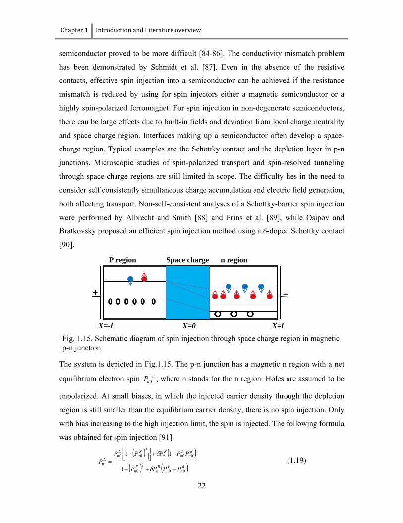
The system is depicted in Fig.1.15. The p-n junction has a magnetic n region with a net
equilibrium electron spin nnP 0 , where n stands for the n region. Holes are assumed to be
unpolarized. At small biases, in which the injected carrier density through the depletion
region is still smaller than the equilibrium carrier density, there is no spin injection. Only
with bias increasing to the high injection limit, the spin is injected. The following formula
was obtained for spin injection [91],
( ) ( )( ) ( )R
nL
nR
nR
n
Rn
Ln
Rn
Rn
Ln
Ln
PPPP
PPPPPP
002
0
002
00
1
11
−+−
−+⎥⎦⎤
⎢⎣⎡ −
=δ
δ (1.19)
n region P region Space charge
+ _
X=-l X=0 X=l
Fig. 1.15. Schematic diagram of spin injection through space charge region in magnetic p-n junction

Introduction and Literature overview Chapter 1
23
where L (left) and R (right) label the edges of the space-charge (depletion) region of a p-n
junction. Correspondingly, RnPδ represents the nonequilibrium electron polarization,
evaluated at R, arising from a spin source.
1.2.3. Active magneto-electronic devices
The spin valve and the magnetic tunnel junction involve ferromagnetic and non
magnetic metal films with or without insulating tunnel barrier. They are compatible with
CMOS technology. But the devices are passive and are not capable to power gain. The
passive devices are adequate for memory applications if the output voltages are
sufficiently large. An active device which have power gain, are of bigger utility and
figure the spine of semiconductor electronics. Recently researches are focused on
integrate spintronics directly with semiconductors by incorporating a semiconductor
spintronics materials in a device structures. This can be able to develop a spintronics
device with power gain and therefore they will be capable to maintain a large fan out
which is necessary to form a high density electronic logic applications.
1.2.3.1. Spin field effect transistor
One attempt to semiconductor spintronics involves a spintronics device and an
application of spin injection theory to semiconducting channel of a field effect transistor
(FET) had proposed by Datta and Das. In Datta-Das structure [92], a ferromagnetic
source and a drain were connected by 2D electron gas channel (2DEG) with a fixed
source to drain distance (Lx) as shown as schematic diagram in Fig 1.16. A
magnetization of both source and drain were oriented along the axis of the channel and an
internal electric field (E) was perpendicular to the 2DEG plane. Carriers were injected at
the source with their spin axis (along x axes) proceed under the applied magnetic field.
By applying a gate voltage to the channel, the internal electric field (E), the effective
magnetic field (H*) and spin phase (φ) can be varied. Increase of gate voltage sweeps the
magnitude of H* to values that causes spin precessions of multiples of π and 2π, and
thereby causes a periodic source to drain conductance. In the past few years, much
research has been carried out involving the spin injection FET using ferromagnetic
semiconductors for spin injection [93], but, unfortunately, these materials cannot be able

Chapter 1 Introduction and Literature overview
24
to show the characteristics necessary for the device applications because of their low
Curie temperatures.
Though the spin injection FET has not yet been realized, progress had been made
and significant problems relating to device applications are understood.
1.2.3.2. Spin diodes
To understand the mechanism of spin injection through the complex heterostructures it is
more convincing to start with magnetic p-n junction. Consider the fact that the electrons
are spin polarized, not holes. Fig.1.17 shows the p-n junction of different magnetic
semiconductor junctions. Spin injection can happen from magnetic n-side [Fig. 1.17(a)]
and spin extraction are expected to happen to the magnetic p-side [Fig. 1.17(b)]. An
external field causes spin splitting of the magnetic n-region and spin up subband is more
populated with carriers. At a low bias (below built-in potential) there is no spin injection.
While there are more spin up carrier in n, the barrier for crossing the space charge region
is exponentially larger for spin up electrons. These two exponential factors cancelled and
there is no net spin injection. As the bias voltage increases, the barrier for crossing the
space charge region reduced and the spin injection become larger. The same effect
pursues the analogous reasoning for spin extraction from a magnetic p-region. Figure
1.17(c) and (d) shows another mechanism for larger magnetoresistance. If non-
equilibrium population of is created in the n-side, the opposing external factors are
minimized and the large spin injection can be expected.
InGaAs
InGaAs
2DEG
Fe contact Fe contact
Gate Source Drain
Fig. 1.16. A schematic diagram of Dutta-Das field effect transistor

Introduction and Literature overview Chapter 1
25
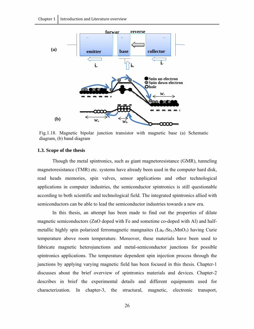
1.2.3.3. Spin bipolar transistor
The more complex and interesting device is the bipolar junction transistor with
non-magnetic n/magnetic p/non-magnetic n emitter-base-collector configuration as
shown in Fig. 1.18 [94]. Forward bias is applied to base to emitter to lowering the base-
emitter barrier for electron. Reverse bias is applied to base to collector which increases
the barrier for electron transport from base to collector. A population of nonequilibrium
spin is maintained at the emitter using circularly polarized light or spin injection from
ferromagnetic electrode. Nonequilibrium spin is maintained through the emitter-base
narrow depletion layer, and it causes nonequilibrium spin at magnetic base region. This
causes a spin split in base which depends on external magnetic field. Carrier
recombination in the base is negligible and the base current is formed by holes flow to the
emitter. On the other hand, collector current depends on the electron spin injection from
emitter to base, and then to collector. Increasing the external field increases the spin
splitting and nonequilibrium spin electron to the base increases. It results a sensitive
current gain in the bipolar junction transistor under applied magnetic field.
PP nnoonnmmaaggnneettiicc
nn nnoonnmmaaggnneettiicc
PP nnoonnmmaaggnneettiicc nn
mmaaggnneettiicc
PP mmaaggnneettiicc nn
ssppiinn--ppoollaarriizzeedd
PP nn NN
X = XP Xn LFig.1.17. Band diagram for magnetic p-n junction; (a) electrons from magnetic n-region, (b) electrons from magnetic p-region, (c) spin injection extraction through spin polarized n to magnetic p-region, (d) The scheme where the spin is injected from magnetic heterostructure N into the non magnetic n-region which forms a p-n junction in with magnetic p-region
(a) (b)
(c) (d)
Chapter 1 Introduction and Literature overview
26
1.3. Scope of the thesis
Though the metal spintronics, such as giant magnetoresistance (GMR), tunneling
magnetoresistance (TMR) etc. systems have already been used in the computer hard disk,
read heads memories, spin valves, sensor applications and other technological
applications in computer industries, the semiconductor spintronics is still questionable
according to both scientific and technological field. The integrated spintronics allied with
semiconductors can be able to lead the semiconductor industries towards a new era.
In this thesis, an attempt has been made to find out the properties of dilute
magnetic semiconductors (ZnO doped with Fe and sometime co-doped with Al) and half-
metallic highly spin polarized ferromagnetic mangnaites (La0.7Sr0.3MnO3) having Curie
temperature above room temperature. Moreover, these materials have been used to
fabricate magnetic heterojunctions and metal-semiconductor junctions for possible
spintronics applications. The temperature dependent spin injection process through the
junctions by applying varying magnetic field has been focused in this thesis. Chapter-1
discusses about the brief overview of spintronics materials and devices. Chapter-2
describes in brief the experimental details and different equipments used for
characterization. In chapter-3, the structural, magnetic, electronic transport,
Fig.1.18. Magnetic bipolar junction transistor with magnetic base (a) Schematic diagram, (b) band diagram
(a)
(b)
emitter collectorbase
forwar reverse
je jbjc
N P N
we wb
wc
Spin up electronSpin down electron hole

Introduction and Literature overview Chapter 1
27
magnetotransport, Hall Effect etc. properties of iron doped ZnO and in some cases co-
doped with Al have been discussed in details. The high crystalline quality epitaxial Fe
doped ZnO dilute magnetic semiconductor thin films deposited on (0001) c-plane single
crystalline sapphire substrates show room temperature ferromagnetic behavior with
carrier mediated ferromagnetism properties where the majority carrier is electron. The
spin injection through the Pt and Fe doped and Al co-doped ZnO junctions have been
estimated from the magnetic field dependent current voltage behavior in chapter-4. The
appearance of positive junction magnetoresistance and dependence of magnetoresistance
on the magnetic moment of ZnO doped with Fe have been explained using
Ferromagnetic/Non-magnetic spin injection theory. Chapter-5 discusses about the
structural, magnetic and electronic properties of non epitaxial La0.7Sr0.3MnO3 thin films
on (100) p-Si substrate. The films show room temperature ferromagnetism with colossal
magnetoresistive behavior. In chapter-6, a detailed study of electrical transport
mechanism through the La0.7Sr0.3MnO3/SiO2/p-Si heterojunction with different type of
SiO2 layers and appearance of junction magnetoresistance have been carried out. The
dependency of junction magnetoresistance on trap charges, leakage currents and defects
in SiO2 have been estimated in this chapter. Chaper-7 deals with the p-n heterojuction
formed using p-type La0.7Sr0.3MnO3 half-metallic ferromagnet and n-type Fe doped ZnO
dilute magnetic semiconductor. The spin injection theory through magnetic
semiconductor p-n junction has been employed to describe the junction
magnetoresistance of such heterostructures.
References
[1] S. A. Wolf, D. D. Awschalom, R. A. Buhrman, J. M. Daughton, S. von Molna´r, M. L. Roukes, A. Y. Chtchelkanova, and D. M. Treger, Spintronics: A Spin-Based Electronics Vision for the Future, Science 294, 1488 (2001). [2] D. D. Awschalom and J. M. Kikkawa, Electron Spin and Optical Coherence in Semiconductors, Phys. Today 52, 33 (1999). [3] Y. Ohno, D. K. Young, B. Beschoten, F. Matsukura, H. Ohno, and D. D. Awschalom, Electrical spin injection in a ferromagnetic semiconductor heterostructure, Nature (London) 402, 790 (1999). [4] R. Fierderling, M. Keim, G. Reushcer, W. Ossau, G. Schmidt, A. Waag, and L. W. Molenkamp, Injection and detection of a spin-polarized current in a light-emitting diode, Nature (London) 402, 787 (1999).

Chapter 1 Introduction and Literature overview
28
[5] E. Johnston-Halperin, D. Lofgreen, R. K. Kawakami, D. K. Young, L. Coldren, A. C. Gossard, and D. D. Awschalom, Spin-polarized Zener tunneling in (Ga,Mn)As, Phys. Rev. B 65, R041306 (2002). [6] M. N. Baibich, J. M. Broto, A. Fert, F. Nguyen Van Dau, F. Petroff, P. Etienne, G. Creuzet, A. Friederich, and J. Chazelas Giant Magnetoresistance of (001)Fe/(001)Cr Magnetic Superlattices, Phys. Rev. Lett. 61, 2472 (1988). [7] G. Binasch, P. Grünberg, F. Saurenbach, and W. Zinn, Enhanced magnetoresistance in layered magnetic structures with antiferromagnetic interlayer exchange, Phys. Rev. B 39, 4828 (1989). [8] M. A. M. Gijs, S. K. J. Lenczowski, and J. B. Giesbers, Perpendicular giant magnetoresistance of microstructured Fe/Cr magnetic multilayers from 4.2 to 300 K, Phys. Rev. Lett. 70, 3343 (1993). [9] W. P. Pratt, Jr., S. F. Lee, J. M. Slaughter, R. Loloee, P. A. Schroeder, and J. Bass, Perpendicular giant magnetoresistances of Ag/Co multilayers, Phy. Rev. Lett. 66, 3060 (1991). [10] A. M. Martin Gijs, E. W. and Gerrit Bauer, Perpendicular giant magnetoresistance of magnetic multilayers, Adv. Phys. 46, 285 (1997). [11] K. Bussmann, S.F. Cheng, G.A. Prinz, Y. Hu, R. Gutmann, D. Wang, R. Beech and J. Zhu, CPP giant magnetoresistance of NiFeCo/Cu/CoFe/Cu multilayers, IEEE Trans. Mag. 34, 924 (1998). [12] W. Oepts, M. A. M. Gijs, A. Reinders, and R. M. Jungblut, R. M. J. van Gansewinkel and W. J. M. de Jonge, Perpendicular giant magnetoresistance of Co/Cu multilayers on grooved substrates: Systematic analysis of the temperature dependence of spin-dependent scattering, Phys. Rev. B 53, 14024 (1996) [13] R. Schad, C. D. Potter, P. Beliën, G. Verbanck, V. V. Moshchalkov, and Y. Bruynseraede, Giant magnetoresistance in Fe/Cr superlattices with very thin Fe layers, Appl. Phys. Lett. 64, 3500 (1994). [14] S. S. P. Parkin, Z. G. Li, and David J. Smith, Giant magnetoresistance in antiferromagnetic Co/Cu multilayers, Appl. Phys. Lett. 58, 2710 (1991). [15] M. Julliere, Tunneling between ferromagnetic films, Phys. Lett. A 54, 225 (1975). [16] P. M. Tedrow and R. Meservey, Spin Polarization of Electrons Tunneling from Films of Fe, Co, Ni, and Gd, Phys. Rev. B 7, 318 (1973). [17] R. Meservey and P. M. Tedrow, Spin-polarized electron tunneling, Phys. Rep. 238, 173 (1994). [18] T. Miyazaki and N. Tezuka, Giant magnetic tunneling effect in Fe/Al2O3/Fe junction, J. Magn. Magn. Mat. 139, L231 (1995). [19] J. S. Moodera, Lisa R. Kinder, Terrilyn M. Wong, and R. Meservey, Large Magnetoresistance at Room Temperature in Ferromagnetic Thin Film Tunnel Junctions, Phys. Rev. Lett. 74, 3273 (1995). [20] N. Tezuka, N. Ikeda, S. Sugimoto, and K. Inomata , 175% tunnel magnetoresistance at room temperature and high thermal stability using Co2FeAl0.5Si0.5 full-Heusler alloy electrodes, Appl. Phys. Lett. 89, 252508 (2006). [21] S. Yuasa, T. Nagahama, A. Fukushima, Y. Suzuki and K. Ando, Giant room-temperature magnetoresistance in single-crystal Fe/MgO/Fe magnetic tunnel junctions, Nature Mater. 3, 868 (2004).

Introduction and Literature overview Chapter 1
29
[22] S. Yuasa, A. Fukushima, H. Kubota, Y. Suzuki and K. Ando, Giant tunneling magnetoresistance up to 410% at room temperature in fully epitaxial Co/MgO/Co magnetic tunnel junctions with bcc Co(001) electrodes Appl. Phys. Lett. 89, 042505 (2006). [23] D. D. Djayaprawira, K. Tsunekawa, M. Nagai, H. Maehara, S. Yamagata, N. Watanabe, S. Yuasa, Y. Suzuki, and K. Ando, 230% room-temperature magnetoresistance in CoFeB/MgO/CoFeB magnetic tunnel junctions, Appl. Phys. Lett. 86, 092502 (2005). [24] Y. M. Lee, J. Hayakawa, S. Ikeda, F. Matsukura, and H. Ohno , Effect of electrode composition on the tunnel magnetoresistance of pseudo-spin-valve magnetic tunnel junction with a MgO tunnel barrier, Appl. Phys. Lett. 90, 212507 (2007). [25] Y. Sakuraba, M. Hattori, M. Oogane, Y. Ando, H. Kato, A. Sakuma, T. Miyazaki, and H. Kubota, Giant tunneling magnetoresistance in Co2MnSi/Al–O/Co2MnSi magnetic tunnel junctions, Appl. Phys. Lett. 88, 192508 (2006). [26] S Yuasa and D D Djayaprawira, Giant tunnel magnetoresistance in magnetic tunnel junctions with a crystalline MgO(0 0 1) barrier, J. Phys. D: Appl. Phys. 40, R337 (2007). [27] R. A. de Groot, F. M. Mueller, P. G. van Engen and K. H. J. Buschow, New Class of Materials: Half-Metallic Ferromagnets, Phys. Rev. Lett. 50, 2024 (1983). [28] R. von Helmolt, J. Wecker, B. Holzapfel, L. Schultz, and K. Samwer, Giant negative magnetoresistance in perovskitelike La2/3Ba1/3MnOx ferromagnetic films, Phys. Rev. Lett. 71, 2331 (1993). [29] S. Jin, T. H. Tiefel, M. McCormack, R. A. Fastnacht, R. Ramesh, and L. H. Chen, Thousandfold Change in Resistivity in Magnetoresistive La-Ca-Mn-O Films, Science 264, 413 (1994). [30] T. Yonehara, K. Sakaguchi, and N. Sato, Epitaxial layer transfer by bond and etch back of porous Si, Appl. Phys. Lett. 64, 2108 (1994). [31] A. Urushibara, Y. Moritomo, T. Arima, A. Asamitsu, G. Kido and Y. Tokura, Insulator-metal transition and giant magnetoresistance in La1-xSrxMnO3, Phys. Rev B 51, 14103 (1995). [32] P. Schiffer, A. P. Ramirez, W. Bao, and S. W. Cheong, Low temperature magnetoresistance and the magnetic phase diagram of La1-xCaxMnO3, Phys. Rev. Lett. 75, 3336 (1995). [33] Y. Tokur, Y. Tomioka, H. Kuwahara, A. Asamitsu, Y. Moritomo, and M. Kasai, Origins of colossal magnetoresistance in perovskite-type manganese oxides, J. Appl. Phys. 79, 5288 (1996). [34] J. D. Boeck, Switching with Hot Spins, Science 281, 357 (1998). [35] G. A. Prinz, Magnetoelectronics, Science 282, 1660 (1998). [36] C. Zener, Interaction between the d-Shells in the Transition Metals. II. Ferromagnetic Compounds of Manganese with Perovskite Structure, Phys. Rev. 82, 403 (1951). [37] H. A. Jahn and E. Teller, Stability of Polyatomic Molecules in Degenerate Electronic States. I. Orbital Degeneracy, Proc. Roy. Soc. A 161, 220 (1937). [38] A. Mauger, C. Godart, The magnetic, optical, and transport properties of representatives of a class of magnetic semiconductors: The europium chalcogenides, Phys. Rep. 141, 51 (1986).

Chapter 1 Introduction and Literature overview
30
[39] H. Ohno, Properties of ferromagnetic III–V semiconductors, J. Magn. Mat. 200, 110 (1999). [40] K. Potzger, Shengqiang Zhou, H. Reuther, A. Mücklich, F. Eichhorn, N. Schell, W. Skorupa, M. Helm, J. Fassbender, T. Herrmannsdörfer, and T. P. Papageorgiou, Fe implanted ferromagnetic ZnO, Appl. Phys. Lett. 88, 052508 (2006). [41] S. K. Mandal, T. K. Nath and A. K. Das, Microstructural, magnetic, and optical properties of Zn1−xMnx/2Cox/2O x=0.1 and 0.2 semiconducting nanoparticles, J. Appl. Phys. 101, 063913 (2007). [42] S.K. Mandal, T.K. Nath, Microstructural, magnetic and optical properties of ZnO:Mn (0.01 ≤ x ≤ 0.25) epitaxial diluted magnetic semiconducting films , Thin Solid Films 515, 2535 (2006). [43] J. K. Furdyna, Dilute magnetic Semiconductor, J. Appl. Phys. 64, R29 (1988). [44] H. Munekata, H. Ohno, S. von Molnar, Armin Segmüller, L. L. Chang, and L. Esaki , Diluted magnetic III-V semiconductors, Phys. Rev. Lett 63, 1849 (1989). [45] S. Koshihara, A. Oiwa, M. Hirasawa, S. Katsumoto, Y. Iye, C. Urano, and H. Takagi, H. Munekata, Ferromagnetic Order Induced by Photogenerated Carriers in Magnetic III-V Semiconductor Heterostructures of (In,Mn)As/GaSb, Phys. Rev. Lett. 78, 4617 (1997). [46] H. Ohno, Making Nonmagnetic Semiconductors Ferromagnetic, Science 281, 951 (1998). [47] M. E. Overberg, B. P. Gila, G. T. Thaler, C. R. Abernathy, S. J. Pearton, N. A. Theodoropoulou, K. T. McCarthy, S. B. Arnason, A. F. Hebard, S. N. G. Chu, R. G. Wilson, J. M. Zavada, and Y. D. Park, Room temperature magnetism in GaMnP produced by both ion implantation and molecular-beam epitaxy, J. Vac. Sc. Tech. B. 20, 969 (2002). [48] M. Hashimoto, Y. K. Zhou, H. Tampo, M. Kanamura and H. Asahi, Magnetic and optical properties of GaMnN grown by ammonia-source molecular-beam epitaxy , J. Crys. Growth 252, 499 (2003). [49] G. Thaler, R. Frazier, B. Gila, J. Stapleton, Mark Davidson, C. R. Abernathy, S. J. Pearton, and C. Segre, Effect of Mn concentration on the structural, optical, and magnetic properties of GaMnN, Appl. Phys. Lett. 84, 1314 (2004). [50] G. Thaler, R. Frazier, B. Gila, J. Stapleton, M. Davidson, C. R. Abernathy, S. J. Pearton, and C. Segre, Effect of nucleation layer on the magnetic properties of GaMnN, Appl. Phys. Lett. 84, 2578 (2004). [51] Zhiyu Liu, J. De Boeck, V. V. Moshchalkov and G. Borghs, Growth and characterization of Al1−XMnXAs (X 4%) magnetic semiconductor: thin film and superlattices, J. Mag. Mag. Mat. 242-245, 967 (2002). [52] R. Frazier, G. Thaler, M. Overberg, B. Gila, C. R. Abernathy, and S. J. Pearton , Indication of hysteresis in AlMnN, Appl. Phys. Lett. 83, 1758 (2003). [53] T. Dietl, H. Ohno, F. Matsukura, J. Cibert, and D. Ferrand, Zener Model Description of Ferromagnetism in Zinc-Blende Magnetic Semiconductors, Science, 287, 1019 (2000). [54] C. Wang, Z. Chen, Y. He, L. Li and D. Zhang, Structure, morphology and properties of Fe-doped ZnO films prepared by facing-target magnetron sputtering system , Appl. Surf. Sc. 255, 6881 (2009).

Introduction and Literature overview Chapter 1
31
[55] T Tamura and H Ozaki, The relationship of the magnetic properties of M (M = Mn, Fe, Co)-doped ZnO single crystals and their electronic structures, J. Phys. Cond. Mat. 21, 026009 (2009). [56] D. L. Hou, R. B. Zhao, Y.Y. Wei, C. M. Zhen, C.F. Pan and G.D. Tang, Room temperature ferromagnetism in Ni-doped ZnO films, Curr. Appl. Phys. 10, 124 (2010). [57] A. Tiwari, M. Snure, D. Kumar, and J. T. Abiade, Ferromagnetism in Cu-doped ZnO films: Role of charge carriers, Appl. Phys Lett. 92, 062509 (2008). [58] S. H. Liu, J. C. A. Huang, C. R. Lin and X. Qi, Electrical transport and ac conductivity properties of hydrogenated annealing V-doped ZnO, J. Appl. Phys. 105, 07C502 (2007). [59] H. Ohno and F. Matsukura, A ferromagnetic III–V semiconductor: (Ga,Mn)As, Solid State Comm. 117, 179 (2001). [60] H. Katayama-Yoshida, K. Sato, Materials design for semiconductor spintronics by ab initio electronic-structure calculation , Physica B 327, 337 (2003). [61] K Sato and H Katayama-Yoshida, First principles materials design for semiconductor spintronics, Semi. Sc Tech. 17, 367 (2002). [62] P. A. Wolf, R. N. Bhatt and A. C. Durs, Polaron-polaron interactions in diluted magnetic semiconductors, J. Appl. Phys. 79, 5196 (1996). [63] A. Kaminski and S. Das Sarma, Polaron Percolation in Diluted Magnetic Semiconductors, Phys. Rev. Lett. 88, 247202 (2002). [64] J. M. D. Coey, M. Venkatesan, C. B. Fitzgerald, Donor impurity band exchange in dilute ferromagnetic oxides, Nature Mat. 4, 173 (2005). [65] T. Dietl, A. Haury and Y. Merle d'Aubigné, Free carrier-induced ferromagnetism in structures of diluted magnetic semiconductors, Phys. Rev. B 55, R3347 (1997). [66] A. Kaminski and S. Das Sarma, Magnetic and transport percolation in diluted magnetic semiconductors, Phys Rev B 68, 235210 (2003). [67] C. Barraud, P. Seneor, R. Mattana, S. Fusil, K. Bouzehouane, C. Deranlot, P. Graziosi, L. Hueso, I. Bergenti, V. Dediu, F. Petroff and A. Fert, Unravelling the role of the interface for spin injection into organic semiconductors, Nature Physics 6, 615 (2010). [68] V. A. Dediu, L. E. Hueso, I. Bergenti and C. Taliani, Spin routes in organic semiconductors, Nature materials 8, 707 (2009). [69] A. R. Rocha, V. M. García-suárez, S. W. Bailey, C. J. Lambert, J. Ferrer and S. Sanvito, Towards molecular spintronics, Nature materials 4, 335 (2005). [70] K. Tsukagoshi, B. W. Alphenaar and H. Ago, Coherent transport of electron spin in a ferromagnetically contacted carbon nanotube, Nature 401, 572 (1999). [71] M. Ouyang and D. D. Awschalom, Coherent Spin Transfer between Molecularly Bridged Quantum Dots, Science 301, 1074 (2003). [72] Z. H. Xiong, Di Wu, Z. Valy Vardeny and Jing Shi, Giant magnetoresistance in organic spin-valves, Nature 427, 821(2004). [73] V. Dediu, M. Murgia, F. C. Matacotta, C. Taliani, S. Barbanera, Room temperature spin polarized injection in organic semiconductor , Solid State Comm. 122, 181 (2002). [74] J. R. Petta, S. K. Slater, and D. C. Ralph, Spin-Dependent Transport in Molecular Tunnel Junctions, Phys. Rev. Lett. 93, 136601 (2004). [75] A.G. Aronov, Spin injection in metals and polarization of nuclei, JETP Lett. 24, 32 (1976).
Chapter 1 Introduction and Literature overview
32
[76] M. Johnson and R. H. Silsbee, Thermodynamic analysis of interfacial transport and of the thermomagnetoelectric system, Phys. Rev. B 35, 4959 (1987). [77] M. Johnson and R. H. Silsbee, Coupling of electronic charge and spin at a ferromagnetic-paramagnetic metal interface, Phys. Rev. B 37, 5312 (1988). [78] P. C. van Son, H. van Kempen, and P. Wyder, Boundary Resistance of the Ferromagnetic-Nonferromagnetic Metal Interface, Phys. Rev. Lett. 58, 2271 (1987). [79] T. Valet and A. Fert, Theory of the perpendicular magnetoresistance in magnetic multilayers, Phys. Rev. B 48, 7099 (1993). [80] A. Fert and H. Jaffrès, Conditions for efficient spin injection from a ferromagnetic metal into a semiconductor, Phys. Rev. B 64, 184420 (2001). [81] S. Hershfield and H. L. Zhao, Charge and spin transport through a metallic ferromagnetic-paramagnetic-ferromagnetic junction, Phys. Rev. B 56, 3296 (1997). [82] G. Schmidt, D. Ferrand, L. W. Molenkamp, A. T. Filip and B. J. van Wees, Fundamental obstacle for electrical spin injection from a ferromagnetic metal into a diffusive semiconductor, Phys. Rev. B 62, R4790 (2000). [83] E. I. Rashba, Theory of electrical spin injection: Tunnel contacts as a solution of the conductivity mismatch problem, Phys. Rev. B 62, R16267 (2000). [84] P. R. Hammar, B. R. Bennett, M. J. Yang, and M. Johnson, Observation of Spin Injection at a Ferromagnet-Semiconductor Interface, Phys. Rev. Lett. 83, 203 (1999). [85] A. T. Filip, B. H. Hoving, F. J. Jedema, and B. J. van Wees, B. Dutta and S. Borghs, Experimental search for the electrical spin injection in a semiconductor, Phys. Rev. B 62, 9996 (2000). [86] H. J. Zhu, M. Ramsteiner, H. Kostial, M. Wassermeier, H. P. Schönherr, and K. H. Ploog, Room-Temperature Spin Injection from Fe into GaAs, Phys. Rev. Lett. 87, 016601 (2001). [87] G. Schmidt, D. Ferrand, L. W. Molenkamp, A. T. Filip and B. J. van Wees, Fundamental obstacle for electrical spin injection from a ferromagnetic metal into a diffusive semiconductor, Phys. Rev. B 62, R4790 (2000). [88] J. D. Albrecht and D. L. Smith, Electron spin injection at a Schottky contact, Phys. Rev. B 66, 113303 (2002). [89] M W J Prins, H van Kempen, H van Leuken, R A de Groot, W Van Roy and J De Boeck, Spin-dependent transport in metal/semiconductor tunnel junctions, J. Phys.: Cond. Mat. 7, 9447 (1995). [90] V. V. Osipov, and A. M. Bratkovsky, Efficient nonlinear room-temperature spin tunneling-emission in ferromagnetsemiconductor heterostructures with extended penetration depth,’’ cond-mat/0307030 (2003). [91] J. Fabian, Igor Žutić and S. Das Sarma, Theory of spin-polarized bipolar transport in magnetic p-n junctions, Phys. Rev. B 66, 165301 (2002). [92] S. Datta and B. Das, Electronic analog of the electro‐optic modulator, Appl. Phys. Lett. 56, 665 (1990). [93] Y. Ohno, D. K. Young, B. Beschoten, F. Matsukura, H. Ohno, D. D. Awschalom, Electrical spin injection in a ferromagnetic semiconductor heterostructure, Nature 402, 790 (1999). [94] J. Fabian, I. Žutić, and S. Das Sarma, Magnetic bipolar transistor, Appl. Phys. Lett. 84, 85 (2004).

Chapter 2
Experimental equipments and techniques

Experimental equipments and techniques Chapter 2
33
2.1. Introduction
In this chapter, we have discussed about detailed experimental techniques and some
major equipments which have been used to carry out our work on oxide thin films and
heterostructures. First we have used pulsed laser deposition (PLD) unit for depositing the thin
films and heterojunctions. The structural and surface morphological characterizations have been
carried out using high resolution x-ray diffraction (HRXRD) technique, high resolution
transmission electron microscope (HRTEM), high resolution field emission scanning electron
microscope (FESEM), energy-dispersive x-ray spectroscopy (EDAX) and near edge x-ray
absorption fine structure (NEXAFS); the optical properties have been studied using UV-VIS
spectrophotometer and magnetic characterizations have been done using superconducting
quantum interference device (SQUID). The electronic-transport, magneto-electronic, Hall Effect
and magneto-transport properties have been investigated using cryogen free high magnetic field
low temperature VTI system with closed cycle helium refrigeration compressor unit. Current and
voltage source-meter have been used for the current – voltage (I-V), resistivity [ρ(T,H)] and Hall
resistivity [ρH(T,H)] etc. characterizations.
2.2. Brief description of used equipments
2.2.1. Thin film deposition unit: Pulsed Laser Deposition (PLD)
The photograph of experimental set up of the PLD system for thin film oxide films and
heterostuctures deposition has been shown in Fig. 2.1.
Fig. 2.1. The experimental set-up of PLD chamber
Chapter 2 Experimental equipments and techniques
34
A. Laser System: COMPexPro™ 201, High-Pulse-Energy KrF Excimer Laser
manufactured by Coherent, Inc. 5100 Patrick Henry Drive, Santa Clara, CA 95054 has been
used for pulsed laser. The wavelength, Pulse Energy and Maximum Average Power of the
laser source are 248 nm (KrF), 700 mJ and 7 W, respectively. Maximum Repetition Rate is
10 Hz.
B. Deposition Chamber: Deposition chamber with software control unit has been
made by Excel Instruments, Mumbai - 93. For substrate temperature we have used PID
Temperature Controller, Dynamic Control System and substrate heater for a maximum
temperature of 850 °C.
C. Vacuum Components: We have used a turbo molecular pump, TMH/TMU 261,
and a rotary vane pump DUO 10/ MC made by Pfeiffer Vacuum Technology AG;
Headquarters/Germany to evacuate the thin film deposition unit to obtain very high vacuum
(~ 10-7 Torr) and to control the oxygen pressure while depositing the various films.
2.2.2. Characterization equipments
Mainly, the structural, surface morphology, optical, magnetic and electrical characterizations have been carried out for all our thin film samples and heterostructures. A brief description of all the techniques used has been presented here.
2.2.2.1. Structural and surface morphology
2.2.2.1.1. High resolution x-ray diffraction technique (HRXRD)
Structural characterizations of our thin films and heterostructures have been carried out
using high resolution x-ray diffractometer (Model: Philips, PW-1729) with monochromatic Cu-Kα
radiation at room temperature. The tube voltage and current have been kept at 40 kV and 30 mA
respectively. The wavelength of the Kα line, which is 1.541Å in this present case, is basically the
weighted average of the wavelengths of its components Kα1and Kα2, Kα1 being twice the wave length
of Kα2 [1],
541.1)554.1540.12(31
=+× (2.1)
In order to obtain as closely monochromatic Kα1 radiation as possible, Ni filter was used to absorb
undesirable Kβ component. During measurements, the resolution of the instrument i.e. 2
1
α
α
KK is 0.5

Experimental equipments and techniques Chapter 2
35
and accuracy of 2θ value is ±0.03o.
2.2.2.1.2. High resolution transmission electron microscopy (HRTEM)
High resolution transmission electron microscopy (HRTEM) images of our films and
heterostructures were recorded employing JEOL, lEM-2010 ultra - high resolution (UHR)
microscope using a LaB6 filament. During experiment the instrument was operated with an
accelerating voltage of electron, E=200 kV. Corresponding relativistic wavelength of electrons
depends on this accelerating voltage E and its value can be obtained using the modified De
Broglie wavelength [2],
[ ] 2/1200 2/12 cmeEeEm
h+
=λ Å (2.2)
where, h is Planck's constant, m0 the rest mass, e the charge of the electron and c the velocity
of light. Thus obtained λ corresponding to E=200 kV, is 0.025 Å. For low magnification
bright field image, this instrument can resolve a minimum dimension of 2 nm of the specimen
under study and the minimum diameter of electron beam can be ~ 20 nm.
2.2.2.1.3. High resolution field emission scanning electron microscopy (FE-SEM)
High resolution field emission scanning electron microscopy (FE-SEM) has been
done using Carl Zeiss SMT Ltd. SUPRATM 40 [Emitter: Thermal field emission type,
Standard Detectors : High efficiency In-lens detector, Everhart-Thomley Secondary Electron
Detector]. The chamber pressure was maintained at ~ 10-5 mbar and gun pressure at~ 10-5
mbar. During experiment the instrument was operated with an accelerating voltage of
electron, E=5.28 kV. Corresponding relativistic wavelength of electrons, as obtained using
Eq. 2.2, is 0.168 Å. This instrument can resolve a minimum dimension of ~ 1 nm at our
working accelerating voltage of E=5.28 kV. We have used gold coated pelletized samples as
specimens for FE-SEM study.
2.2.2.1.4. Energy dispersive x-ray analysis (EDAX)
Energy dispersive x-ray analysis (EDAX) unit of Oxford instruments is attached with
high resolution field emission scanning electron microscope (Carl Zeiss SMT Ltd
.SUPRATM40). During x-ray analysis of our specimen, the working distance was maintained at
15 mm, the chamber pressure at ~ 10-5 mbar and gun pressure at ~ 10-9 mbar. Both point EDAX

Chapter 2 Experimental equipments and techniques
36
and bulk EDAX were performed on our samples, depending, upon specific requirement. We
have employed INCA EDS hardware and INCA software, which provides a stable microanalysis
platform. This EDAX unit promises a < 1 eV shift in peak position and resolution between count
rates of 1 kcps and 10 kcps in microanalysis of our samples.
2.2.2.1.5. X-ray absorption spectroscopy (XAS)
If a high energy x-ray (0.1-100 eV photon energy) excites an electron from core level of
an atom, the resultant photoelectron will jump into unoccupied higher energy states. The created
core hole filled either via an Auger process or by capture of electron from another state which is
then followed by the fluorescent photon. There are three main regions found on a spectrum
generated by XAS data (Figure 2). The dominant feature is called the "rising edge", and is
sometimes referred to as X-ray Absorption Near-Edge Structure (XANES) or Near-edge X-ray
Absorption Fine Structure (NEXAFS). The pre-edge region is at energies lower than the rising
edge. The fluorescent photon or Auger electron which is inelastically scattered photoelectron is
been measured to obtain NEXAFS spectra as shown in Fig. 2.2.
NEXAFS spectra are usually measured either through the fluorescent, in which emitted
photons are monitored, or total electron yield, in which neutralization current is monitored [3].
The XAS spectra are measured for a solid sample with some standard and a comparative study
gives the present states of the element in the system.
x‐ray
Photoelectron
VB
n’
n
n’
n
Fluorescent photon
VB
Auger electron
VB
n’
n
Fig. 2.2. The processes of NEXAFS spectra: (a) photo absorption of an x-ray into a core level followed by photoelectron emission, followed by either (b) filling of the core hole by an electron in another level, accompanied by fluorescence; or (c) filling of the core hole by an electron in another level followed by emission of an Auger electron.
(a) (b) (c)

Experimental equipments and techniques Chapter 2
37
2.2.2.1.6. Atomic force microscope (AFM)
The atomic force microscope (naming by Scanning Probe Microscope (SPM) [Model:
Multiview- 1000TM by Nanonics Imaging Ltd. Malcha Jerusalem 91487 Israel] has been used to
characterized the surface morphology of the thin films. It consists of 70 μm AFM/ NSOM
Scanner, 200 nm×200 nm STM Scanner, Varian Turbo molecular pump and Ion pump, Nd:
YAG Laser for NSOM, Normal Si AFM and also optical fiber tip, Liquid Cell Accessories,
Avalanche Photo Diode, Leica microscope etc. An atomically sharp tip is scanned over a surface
with feedback mechanisms to maintain the tip at a constant force (contact mode), or at constant
oscillation amplitude (non-contact & tapping mode). A laser is focused to the back of the
reflective cantilever. As the tip scans the surface of the sample, moving up and down with the
topographical feature of the surface, the laser beam is deflected into a multi-sectioned PSD
which measures the difference in light intensities and their incident positions to measure the
height of sample surface at that position.
2.2.2.2. Optical characterizations
For optical characterization, absorbance spectra of the nanocrystalline sample are
recorded using UV - visible spectrophotometer (Micro pack, DH-2000, Deuterium Halogen
Light Sources) combine the continuous spectrum of an RF-excited deuterium UV-Visual source
and a halogen VIS-NIR light source in a single optical path (fiber optical path). The combined
spectrum sources produce stable spectral output from ~ 200 - 1200 mm in a compact package).
We have done the global correction of measuring instrument using the bulk ZnO sample with
Integration Time: 5000 msec Average: 10, Box car: 10 and Flash Delay: 100.The global
correction is done through the reflection mode placing the beam of the light at the perpendicular
or 60° angle with the sample surface. After this we have recorded absorbance spectra of all
samples fixing the globalize conditions.
Optical transmission spectra of the thin films are recorded at room temperature in an
energy variation of 1 - 4 eV. The band gaps of all the DMS thin films are estimated from the
measured spectra. The optical absorption measurements are carried out on a large number of
samples of various thicknesses. A steep rise in the absorbance near the absorption edge hints a
direct type transition. In a crystalline material with polycrystalline structure both direct or
Chapter 2 Experimental equipments and techniques
38
indirect optical transitions are possible depending on the band structure of the material.
Assuming parabolic bands, the relation between α and Eg for the direct transition is given by,
ngEhh )( −∝ γγα (2.3)
and for indirect transition by
)/exp(1)(
1)/exp()(
TEEhB
TEEhA
hD
nPg
D
nPg
θν
θν
να−−
−−+
−
+−= (2.4)
where, Ep is the phonon energy assisting the transition, θD the Debye temperature and are
constants: For a direct transition n = 1/2 or 3/2 depending on whether the transition is allowed
or forbidden in quantum mechanical sense. Similarly, n = 2 or 3 for indirect allowed and
forbidden transition, respectively. The usual method of determining band gap is to plot a graph
between nh /1)( να and νh and look for that value of n which gives best linear graph in the band
edge region.
2.2.2.3. Magnetic characterizations
Magnetic measurements [Magnetization (M) as a function of magnetic field (H) and
Magnetization (M) as a function of temperature (T)] have been carried out using Quantum
Design superconducting quantum interferometer device, commonly known as SQUID
magnetometer, in the dc magnetic field range of 0 ± 55 kOe and in the temperature range of 2 -
330 K.
The Quantum Design MPMS SQUID VSM Ever-Cool system is an integrated pulse-tube
cryocooler system. This eliminates the need to use any liquid cryogens for the operation of the
MPMS SQUID VSM. The SQUID VSM utilizes a 7 Tesla, superconducting, helium-cooled
magnet and accomplishes rapid switching between charging and discharging states and stable
fields with a unique superconducting switching element called the Quick Switch, which changes,
between superconducting and normal states in less than one second. This allows rapid collection
of high precision data. Typical M-H loop up to 5 T would take ~ 60 mins and M-T measurement
in the temperature range of 4 – 300 K would take ~70 mins. Temperature Accuracy of the
SQUID is lesser of ±1% or 0.5 K

Experimental equipments and techniques Chapter 2
39
2.2.2.4. Electrical characterization
The electrical characterizations of all our oxides thin films and heterostructures have
been done mainly using the high magnetic field (8 T) cryogen free superconducting magnet
with variable temperature insert (VTI) system which is operated down to 2 K temperature along
with other devices, e.g., Keithley-2182 nanovoltmeter, Keithley-2612 source-meter (with 1µV
resolution) and Keithley-6221 AC and DC current source. Temperature has been controlled using
Lakeshore (Model 331) temperature controller with the temperature stability better than ± 50 mK.
2.2.2.4.1. Cryogen free high magnetic field (Superconducting magnet) VTI system
The photograph of Cryogen free high magnetic field VTI system set up has been shown
in Fig. 2.3 (a) and (b). Figure 2.3 (c) shows the schematic VTI circuit and the probe that has been
used for different electrical measurements has been shown in Fig. 2.3 (d).
The cryogen free high field measurement system combines the latest cryogen free
technology with sophisticated measurement techniques. It is comprised of the following main
components: (1) Cryo-cooler system with compressor, (2) Cryostat and Magnet, (3) Variable
temperature insert (VTI), (3) Electronics rack with measuring devices, (4) Measurement System
Software and (5) Water chiller with compressor for the cooling of the Cryo-cooler compressor.
The cryo-cooler system is the Gifford McMahon (GM) cryocooler which has the
advantage of greater thermodynamic efficiency and reliable operation in any orientation. It uses
(a) (c)
(b)
(d)
Fig. 2.3. (a) and (b) The photograph of Cryogen free high magnetic field VTI system set up. (c) The schematic VTI circuit and (d) the probe that has been used for different electrical measurements.
Chapter 2 Experimental equipments and techniques
40
the compressor to drive moving pistons with regenerators. This cryocooler can provide more
than 50 watts of cooling power on the 60 K stage (the first stage) and up to 1.5 watts of cooling
power at 4 K stage (the second stage). The main function of the first stage is to cool the radiation
shield around the low temperature parts of the system. Cooling for the magnet and the VTI is
provided by the second stage as shown in Fig. 2.3 (c).
2.2.2.4.2. Electrical Measurement Instruments
The electrical characterizations was made mainly using
(i) Keithley 2182 nanovoltmeter: Measure voltage from 1nV to 120V (channel 1); 10nV to
12V (channel 2) with 6 and ½ digit display.
(ii) Keithley 2612 source-meter: Maximum output power and source/sink limits to 30.603 W
per channel maximum. ±20.2 V at ±1.515 A, ±202 V at ±101 mA, four quadrant source
or sink operation. Voltage regulation is 0.01% of range. Load: ±(0.01% of range + 100
μV).
(iii)Keithley 6221AC and DC current source: Current ranges from 2 nA to 100 mA with 0.1
to 0.4% accuracy.
2.2.2.4.3. Temperature readouts and controller Instruments
Lakeshore (Model 331) temperature controller has been used to control and measure the
temperature. It is Proportional-Integral-Derivative type temperature controller (PID) with 0 to
1000 with 0.1 setting (proportional), 1 to 1000 (1000/s) (integral) with 0.1 setting and 1 to 200%
(derivative) with 1% resolution. The sensor is used here is diode (Silicon, GaAlAs Most
thermocouple types RTDs: 100 Ω) Platinum, Platinum, Germanium, Carbon-Glass, Cernox™,
and Rox™ sensor with 50 Ω heater load power.
All the electrical measuring systems are automated using the LABVIEW software
(version 8.5) through GPIB interfacing cables with a PC.
2.3. Brief description of experimental technique
Mainly the electrical characterizations such as resistivity, Hall Effect, magnetoresistance
and current-voltage measurements have been done on oxides thin films and heterostructures in
the entire thesis work along with some optical and magnetic measurements. Brief descriptions of

Experimental equipments and techniques Chapter 2
41
such measuring techniques have been presented here. In order to make these electrical
measurements, low resistance contacts should be made between the films and the connecting
wires in the sample holder. This is done by pressing tiny In (indium) piece onto the sample
corners and then the fine Cu wires are bonded into this for Fe and Fe,Al doped ZnO thin films
grown epitaxially on sapphire substrates. Wire bonding for La0.7Sr0.3MnO3 samples have been
done connecting Ag and Cu wires. Wires bonding for p-Si have been done using Al which have
been deposited by thermal evaporation method. Then the Cu wires have been connected on Al
with Ag paste.
2.3.1. Four probe resistivity measurements
The purpose of the 4-point probe is to measure the resistivity and magnetoresistance of the
films of any semiconductor materials. It can measure either bulk or thin film specimen, each of
which consists of a different expression. The 4-point probe setup for bulk or thick films and thin
films has been shown in Fig. 2.4 (a) and (b).
For bulk or thick film samples where the sample thickness (t) >>spacing between two probes (s) we
can assume a spherical projection of current coming to sample and differential resistance is,
⎟⎠⎞
⎜⎝⎛=Δ
dAdxR ρ (2.5)
If we carry out the integrations between the spaces where voltage is measured (s), we can write,
I
V
Fig. 2.3. (a) Four probe method for measuring resistivity; (b) van der Pauw geometry for measuring resistivity of thin films.
I
V
(a) (b)
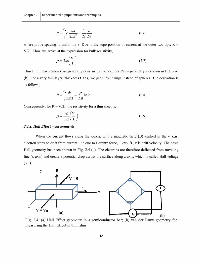
Chapter 2 Experimental equipments and techniques
42
πρ
πρ
221
2
2
1
2 sxdxR
x
x
== ∫ (2.6)
where probe spacing is uniformly s. Due to the superposition of current at the outer two tips, R =
V/2I. Thus, we arrive at the expression for bulk resistivity,
⎟⎠⎞
⎜⎝⎛=
IVsπρ 2 (2.7)
Thin film measurements are generally done using the Van der Pauw geometry as shown in Fig. 2.4.
(b). For a very thin layer (thickness t <<s) we get current rings instead of spheres. The derivation is
as follows,
2ln22
2
1txt
dxRx
x πρ
π== ∫ (2.8)
Consequently, for R = V/2I, the resistivity for a thin sheet is,
⎟⎠⎞
⎜⎝⎛=
IVt
2lnπρ (2.9)
2.3.2. Hall Effect measurements
When the current flows along the x-axis, with a magnetic field (B) applied in the y axis,
electron starts to drift from current line due to Lorentz force, Bev×− , v is drift velocity. The basic
Hall geometry has been shown in Fig. 2.4 (a). The electrons are therefore deflected from traveling
line (x-axis) and create a potential drop across the surface along z-axis, which is called Hall voltage
(VH).
y
z
xj
B
V = VH
V = 0
I
VFig. 2.4. (a) Hall Effect geometry in a semiconductor bar; (b) van der Pauw geometry for measuring the Hall Effect in thin films
(a) (b)
Experimental equipments and techniques Chapter 2
43
For the steady state, we can write following equations for the x and y directions, with e the
electric charge and n the carrier concentration,
xxe eEvm =τ/ (2.10)
)(0 BvEe xy −−= (2.11)
BvE xy = with )/( nejv xx −= and thus,
)/( neBjE xy −= (2.12)
Combining those equations with yH EE = and xjj = yields
neRH
1−= (2.13)
RH is Hall coefficient. The measurement is very complex in case of measuring the thin films and
it can be done by van der Pauw geometry as shown in Fig. 2.4 (b). A series of resistances in the
crossed geometry altering voltage and current directions can be made as a function of magnetic
field. The measured resistances are then multiplied by the film thickness and plotted with
magnetic field. The gradient of the plot gives the Hall coefficient for all the thin film samples.
References
[1] B.D. Cullity Elements of x-ray diffraction, Addison-Wesley Publishing Company Inc., 2nd Edition, California (1978). [2] G. Thomas and M. J. Joringe, Transmission Electron Microscopy of materials, Wiley-Interscience Publication, John Wiley & sons, New York (1979). [3] http://en.wikipedia.org/wiki/XANES.

Chapter 3
Properties of room temperature ferromagnetic Zn(Fe)O
and Zn(Fe,Al)O epitaxial thin film
This chapter is based on
International journals 1. Enhancement of room temperature ferromagnetism of Fe‐doped ZnO epitaxial thin films with Al codoping, T.K. Nath, A.J.
Behan, J.R. Neal, D. Score, Q. Feng, A.M. Fox, G.A. Gehring, Journal of Magnetism and Magnetic Materials vol. 323, pp. 1033 (2011)
2. Temperature dependent carrier induced ferromagnetism in Zn(Fe)O and Zn(FeAl)O thin films by S. Chattopadhyay, T.K. Nath, A.J. Behan, J.R. Neal, D. Score, Q. Feng, A.M. Fox, G.A. Gehring, Applied Surface Science vol. 257, pp. 381 (2010)
3. Extraordinary Hall effect, electronic‐and Magneto‐transport behavior of carrier induced dilute magnetic Zn(Fe)O and Zn(Fe,Al)O thin film by S. Chattopadhyay and T. K. Nath, Physical Review B. (communicated)
Conferences/Symposia 1. Temperature dependent anomalous Hall Effects in DMS Zn(Fe,Al)O epitaxial thin film by S. Chattopadhyay and T. K. Nath,
55th DAE Solid State Physics Symposium 2010 (2010) 2. Magnetoresistive behavior of epitaxial Zinc oxide thin films doped with iron by S. Chattopadhyay, T. K. Nath International
Conference on Magnetic Materials (ICMM‐ 2010) (2010)

Properties of room temperature ferromagnetic Zn(Fe)O and Zn(Fe,Al)O epitaxial thin film
Chapter 3
44
3.1. Introduction
There has been a great interest in transition-metal-doped diluted magnetic
semiconductors (DMS), which exploit both the spin and the charge of carriers, because
the combination of two degrees of freedom promises new functionality of memory,
detectors, light-emitting sources and possible use in next generation spintronic devices,
e.g., spin-valve transistors, spin light-emitting diodes, non-volatile storage and logic
devices. A theoretical study by Dietl et al. [1] has predicted that some of the manganese
doped semiconductors have the ability to be ferromagnetic at or above room temperature
(e.g. GaN and ZnO). The low magnetic ordering temperature in most of the DMS
materials limits the potential spintronic device applications at room temperature. There is
an ongoing quest for ferromagnetic DMS with Curie temperatures, Tc, far in excess of
300 K for the second generation of spin electronics, as well as a search for transparent
ferromagnets which could add an optoelectronic dimension. It is also possible to control
the ferromagnetic interactions between the localized spins by the carriers [2-5], as well as
the demonstration of efficient spin injections into normal semiconductors [6, 7]. In spite
of several progresses on transition metal doped ZnO diluted magnetic semiconductor as a
spintronic material, much controversy remains concerning the mechanism that causes the
ferromagnetism. The carrier-induced ferromagnetism has been observed in different III-V
[8-10] and II-VI [11-14] semiconductors. The interest in ZnO was originally prompted by
theoretical predictions concerning hole mediated magnetism. However, the experimental
work has been almost entirely concerned with n-type materials, which raises important
and interesting scientific issues concerning the carrier-mediated magnetism. DMS are
mixed spin-fermion systems, involving randomly distributed localized magnetic and
mobile carriers in the semiconductor band. With carrier concentration much smaller than
the magnetic impurity concentration, the DMS systems provide a complimentary limit to
Kondo systems. The coupling between localized impurity spin (S) and mobile valence
band holes can be represented by the exchange interaction – J S.σ, where σ is the fermion
spin operator. A theoretical approach has been made by S. Singh et al. [15] to explain the
carrier induced ferromagnetism in DMS system by using diluted Hubbard model. The
origin of FM in these materials is still an issue of debate. In the currently accepted picture
Chapter 3 Properties of room temperature ferromagnetic Zn(Fe)O and Zn(Fe,Al)O epitaxial thin film
45
for DMS the presence of carriers is essential to mediate the interaction between the
magnetic ions. An investigation with additional dopants to enhance or induce
ferromagnetism in these DMS materials will be an interesting approach to establish the
theoretical picture of carrier induced FM.
Some efforts have been made with various doping element to enhance both the
electrical conductivity and ferromagnetism. In some literature the coexistence of
ferromagnetic and paramagnetic component is reported due to some defect states present
in the doped ZnO systems. Sharma et al. [10] observed that there is coexistence of
ferromagnetic contribution and paramagnetic contribution in Zn(Fe)O system and the
paramagnetic behavior increased with increasing doping concentrations. They have
showed it by the Mossbauer spectra for Zn(Fe)O samples recorded at room temperature
in order to probe local magnetic environment around the Fe sites and to determine the
oxidation state of the Fe in ZnO matrix. Each spectrum shows a paramagnetic doublet
with isomer shift (IS). This coexistence of ferromagnetic and paramagnetic components
in other DMS systems has also been established by different researchers [16-18].
In this chapter, a systematic study of carrier concentration dependent room
temperature ferromagnetism (RTFM) in pulsed laser deposited epitaxial thin films of iron
doped zinc oxide [Zn(Fe)O] and iron doped zinc oxide incorporated with 1% aluminium
[Zn(Fe,Al)O] has been presented. We have investigated explicitly the presence of
temperature dependent paramagnetic component and its effect on room temperature
ferromagnetism in Zn(Fe)O and Zn(Fe,Al)O dilute magnetic semiconductors (DMS)
using low temperature SQUID measurements. The structural and optical absorption
properties have also been studied for these DMS thin films. Moreover, the electrical and
magneto-electrical properties have also been investigated for those DMS thin films. The
Anomalous Hall Effect and magnetoresistance behavior of these DMS films have been
studied and the sp-d exchange behavior of such DMS systems in different temperatures
has been found.
3.2. Experimental procedures
3.2.1. Preparation of targets
Required amount of high purity ZnO, Fe2O3 powder has been well mixed with
hand grinder repeatedly and sintered at 450 ºC till the required phase appeared with 5%

Properties of room temperature ferromagnetic Zn(Fe)O and Zn(Fe,Al)O epitaxial thin film
Chapter 3
46
Fe. Required amount of high purity Al2O3 powder were mixed with the ZnO and Fe2O3
powder to dope 5% of Fe and 1% aluminum in the zinc oxide target. The well mixed
powder after repeated grinding is sintered at the same 450 ºC. Finally, the Zn0.95Fe0.05O
and Zn0.94Fe0.04Al0.01O powders were palletized and used as the target for pulsed laser
deposition. The same procedures have been followed to dope ZnO with 7 and 10% Fe
also.
3.2.2. Cleaning of substrates
The c-plane (0001) sapphire substrate has been cleaned repeatedly with De-
ionized water, Acetone and Propanol using ultrasonic vibrator. Each cleaning process has
been carrier out for 20 min.
3.2.3. Preparation of thin films
The films are grown on well cleaned c-plane (0001) sapphire substrate by pulsed
laser deposition technique at several substrate temperatures (300 to 600 ºC) and different
ambient oxygen pressures (from base pressure ~10-5 to 10-1 Torr). The optimized
deposition parameters used in obtaining the Zn(Fe,Al)O films having highest magnetic
moment at room temperature are - substrate temperature of 450 ºC and 10-5 Torr ambient
oxygen atmospheres for 30 min at a laser pulse frequency (repetition rate) of 10 Hz. The
XeCl (λ = 308 nm) pulsed mode excimer laser has been used at an average pulsed laser
energy of 150 mJ.
3.2.4. Characterization of thin films
The concentrations of Fe were estimated by EDAX. The structural studies have
been done by high resolution x-ray diffraction (XRD), cross-sectional High Resolution
Transmission Electron Microscope (HRTEM). Atomic Force Microscope (AFM) image
have been taken for estimate the surface roughness of the films. Room temperature XAS
spectra have been taken to estimate the valence state of Fe ion and the content of metallic
Fe in the films. The magnetic properties have been carried out using SQUID
measurements at room temperature and low temperatures down to 5 K. The thicknesses
of the films have been measured with Dektak profilometer and found to lie in the range of
150 – 450 nm. Hall Effect and magnetoresistance measurements at room temperature and

Chapter 3 Properties of room temperature ferromagnetic Zn(Fe)O and Zn(Fe,Al)O epitaxial thin film
47
low temperature have been performed using the van-der Pauw four-probe configuration
with magnetic fields up to 8 T. The band gap and crystallinity have been estimated using
transmission curve of UV spectroscopy recorded at different temperatures.
3.3. Results and discussions
3.3.1 Chemical properties study
The concentrations of Fe were established by energy dispersive x-ray analysis
(EDAX). The actual values of the Fe concentration in different films have been listed in
the Table-3.1.
Table-3.1: The actual Fe concentration in the Zn(Fe)O and Zn(Fe,Al)O thin films
Sample Actual Fe concentration
Zn(Fe)O with 5% Fe 2.85%
Zn(Fe,Al)O with 5% Fe 3.28%
Zn(Fe)O with 7% Fe 6.12%
Zn(Fe,Al)O with 7% Fe 6.24%
Zn(Fe)O with 10% Fe 8.56%
Zn(Fe,Al)O with 10% Fe 8.51%
3.3.2. Structural properties
In Fig. 3.1(a) the recorded XRD patterns (normal θ - 2θ scan) using Cu-Kα
radiation (λ = 1.542 Å) show that the Zn(Fe)O and Zn(Fe,Al)O films with 5% Fe of
thickness 420 and 300 nm respectively, are perfectly epitaxial on (0001) c-plane sapphire
in the (0001) direction of the films. The observed XRD patterns also confirm that there is
no iron oxide or any other secondary impurity phases present in the films. The ionic radii
of aluminum (Al3+) is smaller compared to zinc (Zn2+) but ionic radii of iron (Fe2+) is
larger than Zn. So on doping with iron in Zn(Fe)O a stress will develop in ZnO. The
FWHM of (0002) film peak and c-axis parameter are obtained to be 0.47˚ and 5.253 Å,
respectively. On co-doping with Fe and Al in ZnO as Zn(Fe,Al)O, the FWHM of (0002)

Properties of room temperature ferromagnetic Zn(Fe)O and Zn(Fe,Al)O epitaxial thin film
Chapter 3
48
film peak is obtained as 0.39˚ and c-axis parameter so obtained is 5.218 Å. The FWHM
and c-axis parameter are found to reduce slightly on co-doping as stress developed due
to doping of Fe and strain developed due to doping with Al. This development of stress
and strain compels the reduction of FWHM and c-axis parameter of the Zn(FeAl)O film
compared to FWHM and c parameter of the Zn(Fe)O film with 5% Fe. The XRD pattern
of Zn(Fe)O and Zn(Fe,Al)O thin films with different doping concentrations have been
shown in Fig. 3.1(b) and Fig.3.1(c), respectively.
Fig. 3.1(d) shows the high resolution transmission electron microscope (HRTEM) image
revealing very sharp film-substrate interface. The d spacing of the film calculated from
the HRTEM image is 0.261 which well matches with the d spacing of (0002) plane of
ZnO. The micrograph taken in [10-10]s || [2-1-10]f zone axes clearly indicates the high
degree of texturing of this epitaxial film with the substrate having an atomically sharp
interface with no mixed layer near the interface.
40 50 60 70
ZnO
2θ (degree)
Zn(Fe)O 5% Fe
Inte
nsity
Zn(FeAl)O 5% Fe
(a)
40 50 60 70
2θ (degree)
Zn(Fe)O 10% Fe
Zn(Fe)O 7% Fe In
tens
ity
(b)Zn(Fe)O 5% Fe
40 50 60
Zn(Fe,Al)O 10% Fe
Zn(Fe,Al)O 7% Fe
Zn(Fe,Al)O 5% Fe
2θ (degree)
(c)
Inte
nsity
Fig. 3.1. (a) The XRD pattern of as grown ZnO, Fe- doped and Fe and Al – doped epitaxial films for 5% Fe. (b) The XRD pattern of Zn(Fe)O epitaxial films for different Fe concentrations. (c) The XRD pattern of Zn(Fe,Al)O epitaxial films for different Fe concentrations. (d) the cross-sectional HRTEM of the junction.
(d)

Chapter 3 Properties of room temperature ferromagnetic Zn(Fe)O and Zn(Fe,Al)O epitaxial thin film
49
Figure 3.2 shows the room temperature XAS spectra for both the Fe and Fe with
Al doped epitaxial films along with some standards. The valence of Fe in both the DMS
films appears to be Fe2+ as the band edge positions are similar to FeO spectra. The small
pre-edge peak of the films is likely due to the less symmetric environment in the Zn site
compared to the octahedral coordination in FeO.
3.3.3. Surface morphology
7110 7120 7130 7140 7150 71600.0
0.5
1.0
1.5
Fe2O3 maghemite Zn(Fe)OZn(FeAl)O FeO Fe2O3 Hametite
Nor
mal
ized
Χμ
(E)
Energy (eV)
Fig.3.2. (a) Room temperature near edges XAS spectra for both Zn(Fe)O and Zn(Fe,Al)O epitaxial films compared to some standards (Fe2O3 – Hematite, Fe2O3 –Maghemite and FeO). The valence looks to be Fe2+ for both the ZnO films.
10.80.60.40.20
1.2
1
0.8
0.6
0.4
0.2
0
X[µm]
Y[µ
m]
39.13 nm
0.00 nm1.41.210.80.60.40.20
1.2
1
0.8
0.6
0.4
0.2
0
X[µm]
Y[µ
m]
54.99 nm
0.00 nm
1.61.41.210.80.60.40.20
1.6
1.4
1.2
1
0.8
0.6
0.4
0.2
0
X[µm]
Y[µ
m]
59.16 nm
0.00 nm
(a) (b)
(c) (d)
(d)
Fig.3.3. (a), (b), (c) The AFM image of Zn(Fe)O and Zn(Fe,Al)O thin films. (d) 3-d view of one of the films.

Properties of room temperature ferromagnetic Zn(Fe)O and Zn(Fe,Al)O epitaxial thin film
Chapter 3
50
The AFM image of the films recorded for 1 µm × 1 µm scan area have been
shown in Fig. 3.3 (a) to (c) for Zn(Fe)O and Zn(Fe,Al)O thin films. The measured r.m.s
roughnesses of the films have been obtained to be 1 to 2 nm. Fig. 3.3 (d) is the 3-d view
of one of the scanned AFM image of Zn(Fe)O film.
3.3.4. Optical properties
To obtain an idea of the band gap of the films and its temperature variation, the
temperature dependent absorption spectra in UV regime have been recorded. The UV
transmission spectrum of Zn(Fe)O and Zn(Fe,Al)O films with 5% Fe at room
temperature are shown in the inset of Fig. 3.4(a). Fig. 3.4(b) and (c) are the same plot for
7 and 10 % Fe concentrations, respectively. The transmittance spectra show the well
crystalline nature (sharp drop at the band edges) of all the films. The band gap is
determined to be about 3.20 eV for all the films at room temperature.
The temperature dependence of the direct band gap, determined from the
absorption edge, can be described well by Varshni’s equation,
βγ+
−=T
TETE gg
2
)0()( (3.1)
The temperature dependent band gap shown in Fig. 3.5(b) can be fitted by Varshni’s
equation with Eg(0) = 3.55 eV, γ = 2.41 meV/K, and β = 935 K. In Varshni’s equation, β
is physically associated with the Debye temperature of the crystal and γ associated with
Fig.3.4. Room temperature transmission spectra of UV absorption spectroscopy for Zn(Fe)O and Zn(Fe,Al)O films (a) 5% Fe, (b) 7% Fe and (c) 10% Fe. (d) Room temperature transmission spectra of UV absorption spectroscopy for Zn(Fe)O films with different Fe concentrations.
200 400 600 800 1000354045505560657075808590
Zn(Fe)O Zn(Fe,Al)O
% T
rans
mitt
ance
Wavelength (nm)
5%
(a)
300 600 90030
40
50
60
70
80
90
(b)
7%
Zn(Fe)O Zn(Fe,Al)O
% T
rans
mitt
ance
Wavelength (nm)300 600 900
30
40
50
60
70
80
90
(c)
10%
Zn(Fe)O Zn(Fe,Al)O
% T
rans
mitt
ance
Wavelength (nm)

Chapter 3 Properties of room temperature ferromagnetic Zn(Fe)O and Zn(Fe,Al)O epitaxial thin film
51
thermal expansion. The Debye temperature obtained for Fe, Al co-doped ZnO is
comparable to bulk undoped ZnO (920 K) [19].
3.3.5. Magnetic properties
The ferromagnetic M(H) behavior of both the Zn(Fe)O and Zn(Fe,Al)O films
grown on sapphire substrate at optimum deposition condition have been characterized
using a SQUID magnetometer in the magnetic field range of 0 - ± 5 T. The SQUID
measurements have been carried out down to 5 K operating temperature.
3.3.5.1. Room temperature magnetic properties
The ferromagnetic M(H) behavior at room temperature of both the Zn(Fe)O films
for different Fe doping concentrations have been shown in Fig. 3.6. The diamagnetic
contributions of sapphire substrate have been subtracted carefully at each magnetic field
from the net magnetization [uncorrected raw data (shown in the inset of Fig. 3.6.)] to
estimate the actual ferromagnetic contribution of each ferromagnetic film at 300 K. After
correcting the substrate contributions in SQUID raw data a ferromagnetic hysteretic
M(H) behavior at room temperature is observed for both the films. The coercive field and
saturation magnetization for the Zn(Fe)O samples have been listed in Table-3.2.
2.0 2.5 3.0 3.5 4.00
200
400
600 10 K 50 K 100 K 150 K 200 K 250 K 300 K 350 K 400 K
(αhν
)2
Energy (eV)
(a)
0 100 200 300 400
3.25
3.30
3.35
3.40
3.45
3.50
3.55
Ban
d ga
p (e
V)
Temperature (K)
(b)
Fig. 3.5. (a) (αhν)2 vs. energy plot of Zn(Fe,Al)O films at different temperatures. (b) Temperature dependent band gap plot for Zn(Fe,Al)O sample.

Properties of room temperature ferromagnetic Zn(Fe)O and Zn(Fe,Al)O epitaxial thin film
Chapter 3
52
Table-3.2: List of saturation magnetization and coercive field of Zn(Fe)O thin films with different Fe concentrations
Fe concentrations in
Zn(Fe)O thin films
Saturation magnetization
(μB/Fe2+)
Coercive field (Oe)
5% 0.18 135
7% 0.04 93
10% 0.02 87
If all the Fe2+ spins are aligned in high moment state one should expect to attain their full
saturation moment value of 4 μB/Fe2+ for all the films. The rather small value for
saturation magnetization suggests that only a small portion of Fe spins are probably
coupled ferromagnetically and that a significant paramagnetic and antiferromagnetic
fraction of Fe remains: this is seen explicitly from the observation that the diamagnetic
term subtracted from the total signal differs from what should be expected for a sapphire
substrate. Moreover, it is also well known fact that the oxygen vacancies produce shallow
donor states (defect states) while the zinc vacancies produce shallow acceptor states in
Fig.3.6. Room temperature ferromagnetic M(H) hysteresis loops for Zn0(Fe)O epitaxial films with 5, 7 and 10% Fe concentrations. Lower inset shows the same M(H) plot at 300 K in low field regime. Upper inset shows the uncorrected (from substrate contribution) SQUID raw data
-10000 -5000 0 5000 10000-0.15
-0.10
-0.05
0.00
0.05
0.10
0.15
10%
7%
5%
M (μ
B/F
e2+ )
H (Oe)
-400 -200 0 200 400
-0.04
-0.02
0.00
0.02
0.04
M (μ
B/F
e2+ )
H (Oe)
-10000 -5000 0 5000 10000-2
-1
0
1
2
M X
10-4
(em
u)
H (Oe)
Zn(Fe)O on sapphire

Chapter 3 Properties of room temperature ferromagnetic Zn(Fe)O and Zn(Fe,Al)O epitaxial thin film
53
ZnO thin films. These states are delocalized due to the hybridization with the Fe d states.
The enhanced electron due to oxygen vacancy accommodates in the minority spin
channel (let say spin up), so minority spin channels become fully occupied e↑ level and
singly occupied t2↑ levels. On the other hand, Zn vacancies introduces holes into the
system, resulting in a completely empty minority spin channel and one hole in the
majority spin channel [18]. If the d orbital is partly occupied, the electrons in that orbital
then hop to the neighboring d orbital, and make the neighboring Fe atoms in parallel spin
configuration. It causes ferromagnetism in the film. On the other hand, if the d cell is
completely occupied, energy starts reduced via hoping process which causes
antiferromagnetic ordering in the system. This may be the cause of the loss of huge
amount of ferromagnetic moment from its expected value in our Fe doped ZnO films.
The low temperature M-H loop establishes the fact that the films may contain high order
of antiferromagnetic and paramagnetic moments. The decrease of ferromagnetic moment
with increasing concentration of iron may be due to the increase of antiferromagnetic
coupling between Fe pairs in the matrix. With increase in the Fe doping in ZnO, the
average distance between adjacent Fe2+ ions reduces. As the antiferromagnetic energy is
less than ferromagnetic energy, the antiferromagnetic coupling between Fe2+⎯Fe2+ ions
dominates at higher Fe concentrations and act as a ferromagnetic moment killer reducing
average magnetic moment per Fe ion. Similar results are obtained for Mn doped and Ni
doped ZnO films [20,21].
3.3.5.2. Low temperature magnetic properties
The temperature dependent M(H) raw SQUID data has been shown in Fig. 3.7(a).
The resulting graph of film magnetization versus magnetic field consists of contributions
from both the sample and the substrate. Measurements of uncoated sapphire substrates
show a large diamagnetic contribution [inset of Fig. 3.7(a)]. The raw SQUID data from a
Zn(Fe)O on sapphire shows two clear contributions [shown in Fig. 3.7(a)]. There is a
prominent low field ferromagnetic contribution from the epitaxial film. A high field
linear dependency with negative slope of diamagnetic contribution from substrate is also
observed. There can be a paramagnetic contribution from unreacted components in the
films which is also linear in this range. To separate out the ferromagnetic contribution

Properties of room temperature ferromagnetic Zn(Fe)O and Zn(Fe,Al)O epitaxial thin film
Chapter 3
54
from the rest, we use the fact that it saturates at higher magnetic fields. The
magnetization is linear above a certain field in the high field region and a straight line
with negative slope can be best fitted. At each temperature the slope of this line has been
calculated from the linear fit and subtracted from each point to leave the ferromagnetic
contribution. Thus obtained the ferromagnetic moment at different temperatures has been
shown in Fig. 3.7(b). The top-left inset of Fig. 3.7(b) shows the clear hysteresis loop at
temperature 5 and 300 K confirms the ferromagnetic behavior of the system. The bottom-
right inset of Fig. 3.7(b) shows the temperature dependent coercive field of Zn(Fe)O
samples.
The change of slope of the raw SQUID [M(H)] data in the high field region with
temperature as shown in Fig. 3.7(a) implies that the films contain not only the
diamagnetic substrate component (which is temperature independent) but also a huge
paramagnetic component in it. To separate out the susceptibility of paramagnetic
component at each temperature we consider that the high field slope of the linear fit
( paradia+χ ) contains both the diamagnetic and paramagnetic components. So,
paradiaparadia χχχ +=+ (3.2)
-40000-20000 0 20000 40000
-6
-4
-2
0
2
4
6
5 K 50 K 100 K 300 K
Mom
ent (
x10-4
emu)
Magnetic field (Oe)
-4 -2 0 2 4
-8
-4
0
4
8
Mom
ent(x
10-4
emu)
Magnetic field (x 104 Oe)
-60000 -40000 -20000 0 20000 40000 60000-1.5
-1.0
-0.5
0.0
0.5
1.0
1.5
5 K 50 K 100 K 300 K
Magnetic field (Oe)
Ferr
omag
netic
mom
ent
(x 1
0-4em
u)
-2000 -1000 0 1000 2000
-0.2
0.0
0.2
5 K 300 K
Magnetic field (Oe)
0 50 100 150 200 250 3000
200
400
600
800
HC (O
e)
Temperature (K)
Fig. 3.7. (a) Raw SQUID data at different temperature of Zn(Fe)O epitaxial thin film grown on c-sapphire substrate. Inset shows the SQUID data of blank substrate. (b) Ferromagnetism in different temperature. The top left inset is the low field hysteresis loop of Zn(Fe)O at temperature 5 K and 300 K. Right bottom inset shows the temperature dependent coercive field.
(a) (b)

Chapter 3 Properties of room temperature ferromagnetic Zn(Fe)O and Zn(Fe,Al)O epitaxial thin film
55
where the slopes from raw SQUID data at a particular temperature in the very high field
regime give paradia+χ . diaχ and paraχ are the susceptibilities of diamagnetic component
from the substrate and film paramagnetic components which is most likely present from
unreacted component in the films. Now, diaχ is a temperature independent parameter and
paraχ depends on temperature with simple Curie law,
TC
para =χ (3.3)
where C is Curie constant and T is temperature in absolute scale (K). Combining Eq.
(3.1) and (3.2) we can write,
diaparadia TCT χχ +=+ (3.4)
The plot of paradiaT +χ with temperature [shown in Fig. 3.8(a)] gives a straight line plot
whose slope and intercept to y-axis gives the diaχ and C, respectively. The constant C
and diaχ has been found to be 8.38×10⁻⁷ emu/Oe/K and -2.74×10⁻⁸ emu/Oe, respectively.
We have also extracted the ferro, para and diamagnetic components of the same Zn(Fe)O
film by employing the M-H curve of blank (uncoated) c-sapphire substrate as shown in
inset of Fig. 3.7(a). The temperature dependent paramagnetic moment has been shown in
Fig. 3.8(b). The comparative studies of diamagnetic, paramagnetic and ferromagnetic
moment at 5 K and 300 K have been shown in upper left and lower right insets of Fig.
3.8(b). The magnetization in ferromagnetic materials is generally expressed as,
)(xJBNgM JBμ= where, Brillouin function ( ) ⎟⎠⎞
⎜⎝⎛−
++= x
JJx
JJ
JJxBJ 2
1coth21)
212coth(
212 and
TkJBgx
B
Bμ= . N is the number of atoms per unit volume, g is the g-factor and μB is the Bohr
magneton. J is described as the total angular momentum quantum number of the
microscopic magnetic moments of the material The saturating nature of paramagnetic
moment at higher fields measured at 5 K fits well with the expression of the
magnetization containing Brillouin function term keeping g =2 as shown in Fig. 3.8 (c).
The rest constant part (NgμB) in the expression of the magnetization has been described
as constant A.

Properties of room temperature ferromagnetic Zn(Fe)O and Zn(Fe,Al)O epitaxial thin film
Chapter 3
56
Table-3.3: Obtained fit parameters from the Brillouin function fit keeping g =2 at different temperatures.
Temperature (K) J A R2(Goodness of fit)
5 1.21 ± 0.04 0.0011 ± 1 х 10-5 0.99975
50 1.19 ± 0.13 0.0008 ± 5 х 10-5 0.99978
100 0.98 ± 0.11 0.0007 ± 4 х 10-5 0.99986
300 0.991 ± 0.12 0.00034 ± 2 х 10-5 0.99979
We get J~1 with excellent goodness of fitting (R2= 0.99975). We have also fitted the
paramagnetic moments with the Brillouin function keeping g = 2 for different
temperatures also. The fitted parameters for different temperatures (5 K, 50 K, 100 K and
0 50 100 150 200 250 300-8
-6
-4
-2
0
Tc d
ia+p
ara
(x 1
0-6)
Temperature (K)
(a)
-10000 -5000 0 5000 10000-8-6-4-202468
(b)
Para
mag
netic
m
omen
t (x1
0-5 e
mu)
Magnetic field (Oe)
5K 50K 100K 300K -8000 -4000 0 4000 8000
-20
-10
0
10
20
Para
Magnetic field (Oe)
Mon
ent (
x 10
-5em
u)
Dia
Ferro
300 K
-70000 -35000 0 35000 70000
-8
-4
0
4
8
DiaFerro
Mom
ent (
x10-4
em
u )
Magnetic field (Oe)
T=5 K
Para
-0.8 -0.4 0.0 0.4 0.8
-8
-4
0
4
8
(c)
Para
mag
netic
mom
ent (
x 10
-4em
u)
μB
/kBT
5 K
0 50 100 150 200 250 300
0.30.60.91.2
02468
II
Temperature (K)
Ms (
x10-4
emu)
(d)
χ par
a (x
10-9
em
u/O
e)
I
Fig. 3.8. (a) The plot of TT paradia −+χ . (b) Extracted paramagnetic moment at different
temperatures. Insets are the comparative study of diamagnetic, paramagnetic and ferromagnetic moments at 5 K (upper left inset) and 300 K (lower left inset) of the same film. (c) The paramagnetic moment at 5 K fitted with Brillouin function keeping g=2. (d) Paramagnetic susceptibility (I) and saturation magnetization (II) vs. temperature plots of Zn(Fe)O film.

Chapter 3 Properties of room temperature ferromagnetic Zn(Fe)O and Zn(Fe,Al)O epitaxial thin film
57
300 K) have been summarized in Table-3.3. The J values obtained from the fit for all
temperatures are found to be ~ 1.0. From the excellent fit (R2 ≈ 1) as shown in Table-3.3,
it concludes that the paramagnetic moments at different temperatures can be fitted well
with a single Brillouin function with a constant value of J (~1). The small value of J
indicates that it does not approach towards classical limits (Langevin function). The
parameters extracted from the Eq. (3.3) and experimental result has been shown in the
Table-3.4. The diamagnetic susceptibility contribution is almost comparable (Table-3.4)
but mismatch of the paramagnetic susceptibilities has been found in the system.
Table-3.4: Comparative study of paramagnetic susceptibilities at different temperatures
Temperature (K)
Paramagnetic susceptibility calculated using the
measurement of diamagnetic susceptibility of sapphire
substrate(-3.11×10⁻⁷ (emu/gm)/Oe)
Paramagnetic susceptibility calculated using the Eq. (3.4).
Calculated diamagnetic susceptibility (-8.32×10⁻⁷
(emu/gm)/Oe)
5 4.43×10⁻⁹ 1.67×10⁻⁷
50 1.78×10⁻⁹ 1.67×10⁻⁸
100 14.73×10⁻¹⁰ 8.35×10⁻⁹
300 3.02×10⁻¹⁰ 2.78×10⁻⁹
The mismatches of the paramagnetic susceptibilities of the films, estimated from Eq. 3.4
and experiment, imply that the simple Curie law cannot be applicable directly for the
DMS systems. The temperature dependent ferromagnetic saturation moment (Ms) and
paramagnetic susceptibility (χpara) has been shown in Fig 3.8 (d). Both ferromagnetic
saturation moment and paramagnetic susceptibility decrease with temperature and they
do not follow standard Curie law (χ ∝ 1/T). A sharp exponential rise of both
ferromagnetic moment and paramagnetic susceptibility in the low temperature regime
reveals more like the insulating type DMS behavior of the film [8,22].
This huge paramagnetic moment may also appear in the films by defects. As
discussed earlier it is well known fact that the oxygen vacancies produce shallow donor
states (defect states) while the zinc vacancies produce shallow acceptor states in ZnO thin
films. These states are delocalized due to the hybridization with the Fe d-states. The

Properties of room temperature ferromagnetic Zn(Fe)O and Zn(Fe,Al)O epitaxial thin film
Chapter 3
58
enhanced electron due to oxygen vacancy accommodates in the minority spin channel
(spin up) of Fe, so minority spin channels become fully occupied eg↑ level and singly
occupied t2g↑ levels. On the other hand, Zn vacancies introduce holes into the system,
resulting in a completely empty minority spin channel and one hole in the majority spin
channel. If the d orbital is partly occupied, the electrons in that orbital then hop to the
neighboring d orbital, and make the neighboring Fe atoms in parallel spin configuration.
It causes ferromagnetism in the film. On the other hand, if the d cell is completely
occupied, energy starts reducing via hoping process which causes antiferromagnetic
ordering in the system.
From the temperature dependent M-H loop in Fig. 3.7(b), it is found that the
magnetization saturates at higher field at lower temperatures compared to same at room
temperature. According to the conventional theory of magnetization when thermal energy
(kBT) is less, the magnetization should saturate at lower fields. But the situation is
completely different in this case. This can be explained by the properties of pinning-type
magnets [23]. In pinning type magnet, the Bloch walls cannot travel freely throughout the
whole grain because of magnetic inhomogeneities present in the grains. These magnetic
inhomogeneities act as pinning centers for the domain walls motion. Apart from the
change in magnetization associated with some wall bending, this pinning will prevent
further magnetization. Wall displacement (other than bending) can occur only when the
force exerted on the wall becomes sufficiently strong. When the strength of the external
field exceeds the pinning field strength then only the saturation magnetization occurs. As
being very low thermal energy in low temperatures the saturation magnetic fields are
higher than the room temperature. So the M-H curve at 300 K saturates earlier than the
curves recorded at lower temperatures.
The isothermal M2 vs H/M plots (Arrott-Belov plot) have been shown in Fig. 3.9
(a) to confirm the presence of intrinsic spontaneous magnetization [M1/β vs. (H/M)1/γ
isothermal plots where β = 0.5 and γ=1 in the mean-field limit]. Each plot clearly shows
the positive intercept at y-axis for all the temperatures confirming the presence of
ferromagnetic spontaneous magnetization in the film for all the temperatures up to 300 K.

Chapter 3 Properties of room temperature ferromagnetic Zn(Fe)O and Zn(Fe,Al)O epitaxial thin film
59
The temperature dependent spontaneous magnetization obtained from Arrott-Belov plots
has been shown in Fig. 3.9 (b). The temperature dependent spontaneous magnetization
curve follows the same sharp rise at low temperature behavior as saturation
magnetization follows with temperature [shown in Fig. 3.8 (d)]. The temperature
dependent behavior of spontaneous magnetization has been found to be similar to an
insulating type DMS material.
3.3.5.3. Carrier dependent ferromagnetism properties
Incorporating 1% of Al in the Zn(Fe)O matrix the room temperature
ferromagnetic component increases almost four times at room temperature as shown in
Fig 3.10(a). However, the understanding of the effect of the additional dopants on the
enhancement of ferromagnetism in the DMSs is still an issue of debate. In some literature
it has been reported that the additional carrier causes enhancement of ferromagnetism
[14]. Li et al. [24] suggest that introducing of Al in Mn doped ZnO results not the
increase of carrier concentration but it could break the metastable structures that formed
in Mn doped ZnO, leading to spinodal decomposition and lead to Mn rich regions.
0 50 100 150 200 250 3000.0
0.2
0.4
0.6
0.8
1.0
1.2
1.4
1.6
1.8
(b)
spon
tane
ous m
agne
tizat
ion
(em
u/g)
Temperature (K)
0.0 4.0x10⁴ 8.0x10⁴ 1.2x10⁵ 1.6x10⁵
10-1
100
300 K
100 K50 K
M2
(em
u2 g-2)
H/M (Oe-g/emu)
Arrott-Belov plot5 K
(a)
Fig. 3.9. (a) Arrott-Belov plots for of Zn(Fe)O epitaxial thin film at different temperatures. (b) Temperature dependent spontaneous magnetization of Zn(Fe)O sample.

Properties of room temperature ferromagnetic Zn(Fe)O and Zn(Fe,Al)O epitaxial thin film
Chapter 3
60
The Mn rich region could be the cause of enhancement of ferromagnetic ordering. In our
case, we observe that the (Fe, Al) doped ZnO films show the higher carrier concentration
( ~ 8.02 × 1026 m-3) than the Fe doped one ( ~ 3.34 × 1026 m-3). The carrier concentrations
of all our DMS films were estimated from the magnetic field dependent Hall voltage
measurements at room temperature. As discussed in XRD results, it has been observed
that the introduction of Al in Fe doped ZnO releases the strain or lattice distortion in our
films. Al in Fe doped ZnO results in increase in its carrier density and also break the
metastable structures that formed in Fe doped ZnO, leading to spinodal decomposition,
which may cause the Fe rich regions. These regions may also be the cause of
enhancement of ferromagnetism due to incorporation of Al in iron doped ZnO films. We
0.0 0.2 0.4 0.6 0.8 1.0 1.2-0.20.00.20.40.60.81.01.21.4
(c)
M (e
mu/
gm)
nc/ni 0.0 0.2 0.4 0.6 0.8 1.0 1.2
0
2
4
6
8
10
(d)χ pa
ra (x
10-9
emu.
gm-1
Oe-1
)
nc/ni
-10000 -5000 0 5000 10000-0.4-0.3-0.2-0.10.00.10.20.30.4
Zn(Fe)O
Zn(FeAl)O
H (Oe)
M (μ
B/F
e2+)
(a)
-10000 -5000 0 5000 10000-0.6
-0.4
-0.2
0.0
0.2
0.4
0.6
(b)
Zn(FeAl)O
Zn(Fe)O
Para
mag
neic
mom
ent
(em
u/gm
)
Magnetic field (Oe)
Fig. 3.10. (a) Room temperature ferromagnetic moment M-H loop of Zn(Fe)O and Zn(Fe,Al)O films, (b) room temperature magnetic field dependent paramagnetic moment contribution of those films. (c) and (d) are carrier dependent (nc/ni) room temperature ferromagnetic moment and paramagnetic susceptibility, respectively.

Chapter 3 Properties of room temperature ferromagnetic Zn(Fe)O and Zn(Fe,Al)O epitaxial thin film
61
have also studied the other Al incorporated films which have much higher carrier
concentrations (listed in Table-3.5).
Table 3.5. Comparative FWHM and carrier concentrations with magnetic moment
Samples Carrier Concentrations
nc/ni FWHM Magnetic moment
Zn(Fe)O 5% Fe 1.61× 10²⁰ 0.076 0.472˚ 0.04000
Zn(Fe)O 5% Fe 2.08× 10²⁰ 0.099 0.471˚ 0.03896
Zn(Fe)O 5% Fe 2.93× 10²⁰ 0.139 0.471˚ 0.08980
Zn(Fe)O 5% Fe 3.34× 10²⁰ 0.158 0.472˚ 0.08560
Zn(Fe,Al)O 5% Fe 3.09× 10²⁰ 0.147 0.394˚ 0.00000
Zn(Fe,Al)O 5% Fe 7.02× 10²⁰ 0.333 0.395˚ 0.38000
Zn(Fe,Al)O 5% Fe 7.64× 10²⁰ 0.362 0.394˚ 0.20500
Zn(Fe,Al)O 5% Fe 1.08× 10²⁰ 0.513 0.393˚ 0.04686
Zn(Fe,Al)O 5% Fe 1.25× 10²⁰ 0.593 0.394˚ 0.01976
Zn(Fe,Al)O 5% Fe 2.22× 10²⁰ 1.051 0.394˚ 0
The XRD study of those films also shows the strain relaxation which should cause the
spinodal decomposition, and hence should enhance the magnetic moment. But, those
films with higher carrier concentrations show lower moment which contradict the
previously discussed ‘spinodal decomposition’ theory [24]. Hence, the observation of
room temperature ferromagnetic behavior in our DMS films probably can be best
explained through the standard theory of carrier induced ferromagnetism. Carrying out
the low temperature SQUID measurements and separating out the diamagnetic,
paramagnetic, ferromagnetic components as already discussed above, it is clearly seen
that the ferromagnetic exchange interaction (magnetization) increases with carrier
concentration and reaches to a maximum beyond which it falls drastically at higher
carrier concentrations as shown in Fig. 3.10(c). Standard theory of DMS predicts that the
exchange is maximized when the nc/ni ratio is in between 0.3 to 0.5 [14]. The reduction of
the moment with increasing carrier density ratio of the films occurs when nc/ni > 0.4. In
addition, from the low temperature SQUID analysis the extracted paramagnetic

Properties of room temperature ferromagnetic Zn(Fe)O and Zn(Fe,Al)O epitaxial thin film
Chapter 3
62
susceptibility with carrier concentration shows exactly opposite nature as shown in Fig.
3.10(d).
The defect such as anion vacancy plays an important role in ferromagnetism in
ZnO as this defect forms shallow donor and provides n-type conduction. Zn interstitial is
also cause the shallow donor level. The cation vacancy can introduce an electronic defect
on neighboring oxygen and creates an O-2p5 anion. The oxygen vacancies are strongly
correlated, and they can form extended molecular orbit around the defect site, which
couples ferromagnetically. The proposed electronic structure with impurity band splits at
higher Curie temperature has been proposed by Coey et al. [25] as shown in Fig. 3.11(a).
Doping with Fe2+ splits d level of shallow impurity band which moves down to the 2p
band of oxygen. Hence, two region forms: one near the beginning of the series where 3d↑
state cross Fermi level in the impurity band, and one towards the end where 3d↓ state
d4↑ d4↑ d4↑ d4↑
d4↑ d4↑ d4↑ d4↑
d4↑ d4↑ d4↑ d4↑
d4↑ d4↑ d4↑ d4↑
d5↑ d5↑ d5↑ d5↑
d5↑ d5↑ d5↑ d5↑
d5↑ d5↑ d5↑ d5↑
d5↑ d5↑ d5↑ d5↑
d5↑ d10 d10 d5↑
d10 d10 d10 d10
d10 d10 d10 d10
d5↑ d10 d10 d5↑
(a) (b)
(c) (d)
e- e-
Fig.3.11.(a) Electronic band structure for high Tc oxides proposed by Coey et al. [25], (b) The magnetic region in Zn(Fe)O sample. (c) After introducing excess carrier to the system within the limit. The excess electrons sit on the unfilled d state and enhance the up spin population of the polarons. (d) Condition when the carrier density is much higher. The carrier density is higher (cross the limit of nc/ni) the d cell starts to be filled by electrons and decreases up spin population. It causes decrease of magnetic moment. When the electron concentration is very high the d cells of maximum polarons become completely filled and the polaron-polaron distance increases which causes reduction of magnetic moment.

Chapter 3 Properties of room temperature ferromagnetic Zn(Fe)O and Zn(Fe,Al)O epitaxial thin film
63
cross the Fermi level. If the impurity band is sufficiently narrow, the donor electrons
become localized and interact with core spin. Hence, if the localized electron interacts
with many magnetic cations it shows completely spin polarization. As the net moment of
iron doped samples are much less as expected (4µB), one can concludes that the localized
electrons are not completely able to interact with all magnetic cations. We also observed
that with increasing carrier concentration the magnetization increases. But additional
doping of electron kills the magnetic moment beyond a certain value of carrier
concentration (nc/ni ~ 0.4). In Fig. 3.11(b), (c) and (d) we have discussed this mechanism.
The iron doped ZnO films contains magnetic cation with partially filled d4 states (Fig.
3.11(b)). The magnetization occurs from the interaction of those cations with localized
electrons. If free carrier increased in the limit nc/ni < 0.4, the additional electrons transfers
to the unfilled d cell and increase net magnetic moment (Fig 3.11(c)). If the carrier
concentrations increases further beyond the limit, the excess carriers enter to d states and
decreases half field d shell. Net magnetization starts decreasing. At very high carrier
concentration d shells become completely filled and net Fe2+ ions available in the system
is reduced. So, the distance between nearest magnetically active ions become so large
that cannot mediate long range magnetic ordering. The films become eventually
paramagnetic in nature.
3.3.6. Electrical properties
The presence of magnetic ions such as 3d transition metal (TM) ions in these
materials leads to an exchange interaction between traveling sp band electrons or holes
and the d electron spins localized at the magnetic ions, resulting in versatile magnetic-
field-induced functionalities [26]. DMS based materials demonstrated several spin related
phenomena such as a spin-polarized transport and luminescence attributable to a sp-d
exchange interaction [27]. In the recent years, ZnO based dilute magnetic semiconductors
have attracts a lot because of huge controversy between the DMS researchers. So, ZnO
based DMS study has a great opening for the researchers.
The anomalous Hall Effect (AHE) has been recognized as a powerful technique
for demonstrating the ferromagnetic ordering to be intrinsic due to spin-polarized
carriers, which mediate ferromagnetic exchange interaction with localized magnetic

Properties of room temperature ferromagnetic Zn(Fe)O and Zn(Fe,Al)O epitaxial thin film
Chapter 3
64
moments. AHE is well-known to be caused by the emergence of voltage transverse to
both an applied current and an external magnetic field proportional to magnetization [28].
The anomalous Hall Effect is attributed to asymmetric scattering involving in spin orbit
interaction between conduction electrons and the magnetic moments [29,30]. So this
analysis is widely used to study the magnetic behavior of dilute magnetic semiconductors
[31,32]. However, the exact mechanism is not clear so far. The questions arise whether
the mechanism is intrinsic or extrinsic. Karplus and Luttinger [33] have proposed the
phenomenon of Anomalous Hall Effect is intrinsic. On the other hand, some theories
attribute the impurity scattering modified by spin orbit interaction namely the skew
scattering [34] and the side jump mechanism [35]. This extrinsic mechanism is rather
complicated and depends on the impurities and band structures of the DMS materials
[36].
One of the characteristics of features of magnetic semiconductors is the sp-d
exchange between sp band of the semiconductor and the localized d electrons associated
with magnetic ions. Magneto-transport measurements in the DMS systems are
extensively used for studying the sp-d interactions of ferromagnetic semiconductors [37,
38]. It is well known fact that the magneto-transport is completely dependent of free
carrier concentration of n-type ferromagnetic semiconductors like ZnO [39-41]. The
change in carrier concentrations and as well as temperature the characterization of wave
function changes from delocalized to localized states which are responsible for change in
magnetoresistances (MR) in the DMS systems [42]. Several different mechanisms have
been proposed for the spin-dependent MR effect [43,44]. One of the mechanisms is the
formation of magnetic polarons [45]. The concept of magnetic polarons can be
understood as the variations in the magnetization created by those doped magnetic ions
around the localized carriers [46]. If the electrons want to travel through the lattice with
low resistance, it must carry the same spin polarization as the surrounding magnetization.
Clearly, the transport behavior is influenced by the magnetization condition of the films.
3.3.6.1. Electrical transport properties
The temperature dependent resistivity of the films has been shown in Fig. 3.12 for the
temperature range of 1.5 to 300 K. The resistivity drops with temperature for all the

Chapter 3 Properties of room temperature ferromagnetic Zn(Fe)O and Zn(Fe,Al)O epitaxial thin film
65
films. Figure 3.12(a) and Fig. 3.12(b) are the temperature dependent resistivity plot of the
Zn(Fe)O and Zn(Fe,Al)O films with different iron doping.
The conduction mechanism in these DMS films can be best explained by the combination
of three types of conduction models
(i) variable range hopping (VHR),⎥⎥
⎦
⎤
⎢⎢
⎣
⎡
⎟⎟⎠
⎞⎜⎜⎝
⎛−=
4/10
0 expT
TVRH
VRHVRH σσ (3.5),
which describes carrier hopping in localized states.
(ii) Efro’s variable range hopping (EVRH), ⎥⎥
⎦
⎤
⎢⎢
⎣
⎡
⎟⎟⎠
⎞⎜⎜⎝
⎛−=
2/10
0 expT
TEVRH
EVRHEVRH σσ
(3.6) due to the electron-electron Coulomb interaction at lower
temperature range.
0 50 100 150 200 250 3002.0x10-4
3.0x10⁻⁴
4.0x10⁻⁴
5.0x10⁻⁴
6.0x10⁻⁴
7.0x10⁻⁴
8.0x10⁻⁴
10% Fe
7% Fe
ρ (Ω
m)
Temperature (T)
Zn(Fe)O
5% Fe
0 50 100 150 200 250 3006.0x10-5
8.0x10⁻⁵
1.0x10⁻⁴
1.2x10⁻⁴
1.4x10⁻⁴
1.6x10⁻⁴
1.8x10⁻⁴
2.0x10⁻⁴
2.2x10⁻⁴
2.4x10⁻⁴
10%Fe7%Fe
ρ (Ω
m)
Temperature (K)
Zn(FeAl)O
5% Fe
4 5 6 7 8 9 10-10.0
-9.6
-9.2
-8.8
-8.4
-8.0
-7.6
-7.2
Zn(FeAl)O
Zn(Fe)O
ln (ρ
)
1000/T (K-1)
0.2 0.3 0.4 0.5 0.6 0.7 0.8-10.8-10.4-10.0-9.6-9.2-8.8-8.4-8.0-7.6-7.2
Zn(FeAl)O
ln (ρ
)
T-1/4 (K-1/4
)
Zn(Fe)O
0.120 0.144 0.168 0.192-9.6-9.2-8.8-8.4-8.0-7.6-7.2
Zn(FeAl)O
Zn(Fe)O
T-1/2(K-1/2)
ln (ρ
)
Fig. 3.12. (a) Temperature dependent resistivity plot of Zn(Fe)O thin films with 5, 7 and 10% Fe, (b) The same plot for the 1% Al incorporated samples, (c) ln(ρ) - T-1/4 plot of Zn(Fe)O and Zn(Fe,Al)O thin films with 5% Fe to test the VRH mechanism. Inset is the ln(ρ) - T-1/2 plot of those same films to test the EVRH mechanism and (d) ln(ρ) -1000/T plot of those samples which satisfies the thermal excitation process of transport.
(a)
(b)
(c) (d)
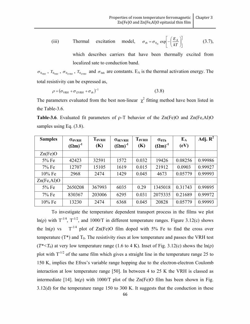
Properties of room temperature ferromagnetic Zn(Fe)O and Zn(Fe,Al)O epitaxial thin film
Chapter 3
66
(iii) Thermal excitation model, ⎥⎦
⎤⎢⎣
⎡⎟⎟⎠
⎞⎜⎜⎝
⎛−=
kTE A
th thexp0σσ (3.7),
which describes carriers that have been thermally excited from
localized sate to conduction band.
VRH0σ , VRH
T0 , EVRH0σ ,
EVRHT0 and th0σ are constants. EA is the thermal activation energy. The
total resistivity can be expressed as,
( ) 1−++= thEVRHVRH σσσρ (3.8)
The parameters evaluated from the best non-linear χ2 fitting method have been listed in
the Table-3.6.
Table-3.6. Evaluated fit parameters of ρ-T behavior of the Zn(Fe)O and Zn(Fe,Al)O
samples using Eq. (3.8).
Samples σ0VRH (Ωm)-1
T0VRH (K)
σ0EVRH (Ωm)-1
T0VRH (K)
σ0Th (Ωm)-1
EA (eV)
Adj. R2
Zn(Fe)O 5% Fe 42423 32591 1572 0.032 19426 0.08256 0.99986 7% Fe 12707 15105 1619 0.015 21912 0.0903 0.99927 10% Fe 2968 2474 1429 0.045 4673 0.05779 0.99993
Zn(Fe,Al)O 5% Fe 2650208 367993 6035 0.29 1345018 0.31743 0.99895 7% Fe 830367 203006 6295 0.031 2075335 0.21689 0.99972 10% Fe 13230 2474 6368 0.045 20828 0.05779 0.99993
To investigate the temperature dependent transport process in the films we plot
ln(ρ) with T-1/4, T-1/2, and 1000/T in different temperature ranges. Figure 3.12(c) shows
the ln(ρ) vs T-1/4 plot of Zn(Fe)O film doped with 5% Fe to find the cross over
temperature (T*) and T0. The resistivity rises at low temperature and passes the VRH test
(T*<T0) at very low temperature range (1.6 to 4 K). Inset of Fig. 3.12(c) shows the ln(ρ)
plot with T-1/2 of the same film which gives a straight line in the temperature range 25 to
150 K, implies the Efros’s variable range hopping due to the electron-electron Coulomb
interaction at low temperature range [50]. In between 4 to 25 K the VRH is classed as
intermediate [14]. ln(ρ) with 1000/T plot of the Zn(Fe)O film has been shown in Fig.
3.12(d) for the temperature range 150 to 300 K. It suggests that the conduction in these

Chapter 3 Properties of room temperature ferromagnetic Zn(Fe)O and Zn(Fe,Al)O epitaxial thin film
67
thin films is due to the thermally assisted tunneling of the charge carriers through the
grain boundary barrier and transition from donor level to conduction band. The transport
mechanism at different temperature ranges has been tabulated in Table-3.7.
Table-3.7. The summarized transport mechanism in different temperature ranges
Sample Temperature Range
Transport mechanism
Best fit R2 value
Zn(Fe)O 1.6-5 K Variable range hopping [T* < T0]
VRH test passed
5 -40 K Intermediate[T* >T0] VRH test failed 40-150 K Efros’s VRH
[ρ = ρ0 exp (T0/T)1/2 ] 0.970
150 – 300 K Thermal excitation
[ρ ~1000/T] 0.0987
Zn(Fe,Al)O 1.6-5 K Variable range hopping [T* < T0]
VRH test passed
5 -40 K Intermediate [T* >T0] VRH test failed 40-150 K Efros’s VRH
[ρ = ρ0 exp (T0/T)1/2 ] 0.988
150 -300 K Thermal excitation [ρ ~1000/T]
0.0992
3.3.6.2. Hall Effect study
The hall resistivity with magnetic field plot of Zn(Fe,Al)O film with 5% Fe at
different isothermal temperatures has been shown in Fig. 3.13(a). Fig. 3.13(b) and Fig.
3.13(c) are the same plot of the Zn(Fe)O and Zn(Fe,Al)O, respectively for different iron
concentrations at 2 K and 300 K (corresponding insets). All the films show the n-type
nature of the films. Saturating nature of the Hall resistivity at higher magnetic field range
in Fig. 3.13(a) confirms the anomalous Hall Effect behavior of iron doped epitaxial ZnO
films. The anomalous Hall Effect can be described by,
MRBR sH 00 μρ += (3.9)

Properties of room temperature ferromagnetic Zn(Fe)O and Zn(Fe,Al)O epitaxial thin film
Chapter 3
68
Where, Hρ , R0 and Rs are the Hall resistivity, ordinary Hall co-efficient and
anomalous Hall co-efficient, respectively. M is the magnetization of the film. The plot of
ordinary Hall co-efficient with temperature of all the films evaluated from temperature
dependent Hall measurements have been shown in Fig. 3.13(d) and its insets.
3.3.6.2.1. Ordinary Hall Effect
From the ordinary Hall co-efficient one can easily find the carrier concentrations and Hall
mobility of these DMS films. The calculated temperature dependent carrier concentration
of Zn(Fe)O and Zn(Fe,Al)O films for different iron concentrations have been plotted in
Fig. 3.14(a) and Fig. 3.14(b), respectively. The increase of carrier concentration with
0 2 4 6 80.0
0.5
1.0
1.5
2.0 2 K 5 K 10 K 50 K 100 K 150 K 200 K 250 K 300 K
ρ hall (
μΩ-m
)
B (T)
Zn(Fe,Al)O with 5% Fe
(a)
0 2 4 6 80.00.51.01.52.0
2.53.03.5
5% 7 % 10%
ρ hal
l (Ω
−m)
B (T)
T = 2 K
Zn(Fe)O
(b)
0 2 4 6 80.0
0.1
0.2
0.3
0.4
0.5
ρ ha
ll(μΩ
−m)
B (T)
T = 300 K
0 1 2 3 4 5 6 7 8 90.0
0.5
1.0
1.5
2.0
2.5(c) 5%
7% 10%
ρ hall (μ
Ω-m
)
B(T)
T =2 K
Zn(Fe,Al)O
0 2 4 6 80.0
0.1
0.2
0.3
ρ hall (μ
Ω−m
)
B (T)
T =300 K
0 50 100 150 200 250 3000.0
0.1
0.2
0.3
0.4
0.5
(d)
R0 (
m3 /C
)
Temperature (T)
Zn(Fe)O
0 50 100 150 200 250 3000.0
0.1
0.2
0.3
0.4
0.5 5% Fe 7% Fe 10% Fe
R0 (
μΩ−m
)
Temperature (T)
Zn(FeAl)O
Fig.3.13. (a) Magnetic field dependent Hall resistivity of Zn(Fe,Al)O thin film with 5% Fe measured at different isothermal temperatures. (b) and (c) are the magnetic field dependent Hall resistivity plots of Zn(Fe)O and Zn(Fe,Al)O thin films, respectively for different Fe concentrations measured at 2 K. Corresponding insets are the same plots measured at 300 K. (d) Temperature dependent ordinary Hall co-efficient of Zn(Fe)O thin films with different Fe concentration. Inset is the same plot for Zn(Fe,Al)O sample.

Chapter 3 Properties of room temperature ferromagnetic Zn(Fe)O and Zn(Fe,Al)O epitaxial thin film
69
temperature shows semiconducting behavior of the films. To analyze the temperature
dependent carrier concentration behavior we have used the multi-donor charge balance
equation so that shallow electrically active defect concentrations and activation energies
could be extracted [47].
For non-degenerate n-type conduction, the charge balance equation adopts the form,
∑=
−
⎟⎟⎠
⎞⎜⎜⎝
⎛ Δ+
=+k
i
B
Di
c
Di
DiA
TkE
NnTg
NNn
12/3
exp1 (3.10)
where n is the carrier concentration, NA is the total acceptor concentration and NDi, ΔEDi
and gDi are the concentration, activation energy and donor degeneracy factor of the ith
donor Di, respectively. We consider gDi = 2, NC is the effective density of states in the
0 100 200 300 400 5000.00.20.40.60.81.01.21.41.61.8
FeAl5 FeAl7 FeAl10
n (x
1026
m-3
)
1000/T0 100 200 300 400 500
0.00.20.4
0.60.8
1.01.21.4
1000/T
n (x
1026
m-3
) Fe5 Fe7 Fe10
0 50 100 150 200 250 3001
2
3
4
5
6
7
Hal
l mob
ility
(x10
-4 m
2 /V-s
)
Temperature (K)
Zn(Fe)O
0 50 100 150 200 250 3004
8
12
16
20
24
28
H
all m
obili
ty (x
10-4
m2 /V
-s)
Temperature (K)
Zn(Fe,Al)O
(a) (b)
(c) (d)
Fig. 3.14. (a) and (b) are the carrier concentration evaluated from R0 plot with 1000/T for Zn(Fe)O and Zn(Fe,Al)O thin films with different Fe doping. (c) and (d) are the Hall mobility of those films.

Properties of room temperature ferromagnetic Zn(Fe)O and Zn(Fe,Al)O epitaxial thin film
Chapter 3
70
conduction band at 1 K given by 2/32* ))2/((2 hπBc kmN = , where m* is the density of states’
effective mass, kB is Boltzmann’s constant. To fit the temperature dependent carrier
concentration we have considered that the acceptor concentration is very less and ND ≈ n.
The fitted parameters for k = 2 have been shown in the Table-3.8.
Table-3.8. The evaluated fit parameters from temperature dependent carrier concentration using Eq. (3.10)
Sample ND1 (m-3) ND2 (m-3) ED1 (meV) ED2 (meV)
Zn(Fe)O 5% 1.07х1028 3.47 х1025 181.79 217.41
7% 9.83 х1027 1.89 х1025 133.61 156.15
10% 2.15 х1028 1.61 х1025 151.79 208.26
Zn(Fe,Al)O 5% 1.09 х1028 3.9 х1025 75.59 315.80
7% 2.16 х1028 3.36 х1025 108.92 333.59
10% 9.54 х1026 1.30 х1025 545.11 72.89
The temperature dependent Hall mobility has been plotted in Fig. 3.14(c) and Fig.
3.14(d) for Zn(Fe)O and Zn(Fe,Al)O, respectively. The mobility first decreases with
increasing temperature up to a certain temperature. After that it starts to increase up to a
certain temperature and then starts decreasing. The mobility of electrons in non-
degenerate single crystal ZnO is limited primarily by scattering due to ionized impurities,
deformation potential and piezoelectric acoustic phonons, and polar optic phonons. Grain
boundary scattering has to be considered as well for such films. The carrier mobility also
depends on free carrier concentration of the films. At very low temperature range the
electron-electron scattering dominates over other. With increasing temperature free
carrier concentration increases and causes a decrease of mobility. The electron-electron
collision do not affect the current density directly as they can not alter the total
momentum. They just randomize the carrier distribution and the momentum randomly
distributed to different velocity groups. The electron-electron collision gives rise to a net

Chapter 3 Properties of room temperature ferromagnetic Zn(Fe)O and Zn(Fe,Al)O epitaxial thin film
71
transfer of momentum, and results greater rate of momentum transfer and lower the
mobility. The electron-electron scattering mobility is inversely proportional to free
electron concentration [ )(/1 Tnee ∝−μ ] [48]. In the comparatively higher temperature
range the electron-electron scattering does not dominates and the impurity scattering as
well as grain boundary scattering starts to dominate. In the moderate low temperature
region impurity scattering dominates. With increasing temperature the localized impurity
scattering start decrease which causes an increase of mobility. The impurity scattering is
given by [49],
1
2
222/31ln
−
⎥⎥⎦
⎤
⎢⎢⎣
⎡
+−⎟
⎟⎠
⎞⎜⎜⎝
⎛+=
BTNBT
NBT
NAT
IIIIμ (3.11)
Where, A and B are constants and NI is the ionized impurity scattering. The electron can
face some grain boundary scattering also. The mobility due to grain boundary scattering
is given by,
( )Tk BBB /exp0 φμμ −= (3.12)
where Tklcq B8/0 =μ . The l is the grain size and 2/1* )/8( mTkc B π= is the thermal
velocity. Bφ is the effective barrier height between two grains. At higher temperature
lattice scattering dominates which causes again decrease of mobility. The temperature
dependent mobility due to lattice scattering can be expressed as [50], α
μ ⎟⎠⎞
⎜⎝⎛=
TDCL (3.13)
Where C, D and α are constants. The total Hall mobility can be expressed using
Matthiessen’s rule,
LBIeeH μμμμμ11111
+++=−
(3.14)
3.3.6.2.2. Anomalous Hall Effect
Figure 3.15(a) shows the temperature dependence of anomalous Hall coefficient,
Rs of the Zn(Fe,Al)O film with 5% Fe, exhibiting decrease of Rs with increasing
temperature. The observation of anomalous Hall Effect in this DMS film also provides

Properties of room temperature ferromagnetic Zn(Fe)O and Zn(Fe,Al)O epitaxial thin film
Chapter 3
72
evidence of intrinsic carrier-mediated ferromagnetism [51]. The AHE observed in other
Zn(Fe)O and Zn(Fe,Al)O films with higher Fe doping is very weak compared to
Zn(Fe,Al)O film with 5% Fe. One of the possible reasons might be the relatively large R0
and low magnetic moments in other Zn(Fe)O and Zn(Fe,Al)O thin films due to smaller
carrier concentration [52]. The origin of the anomalous Hall Effect is believed to be the
spin-orbit interaction between the carrier angular momentum and the localized spin. Rs
has a power law relationship with the ohmic resistivity and is given by,
ns CR ρ= (3.15)
where, C is a constant. The exponent n=1 corresponds to the skew scattering and n=2
corresponds the quantum mechanical side jump scattering [53]. Considering the both
mechanism one can write [54],
2ρρ sjsks baR += (3.16)
where Masksk 0~ μφ represents the average deflection of a charge carrier at a scattering
center. The bsj is associated with a side-jump mechanism where the charge carrier’s
trajectory is displaced a fixed distance perpendicular to its original path at each scattering
centers.
1.0x10⁻⁴ 1.5x10⁻⁴ 2.0x10⁻⁴ 2.5x10⁻⁴
0.00
0.01
0.02
0.03
R s=aρ
+bρ2
Rs (m
3 /C)
ρ (Ω-m)
Rs=bρ2
(b)
0 50 100 150 200 250 300
0.00
0.01
0.02
0.03
Rs (
m3 /C
)
Temperature (K)
(a)
Fig. 3.15. (a) Anomalous Hall co-efficient (Rs), evaluated from Fig. 3.13(a), plot with temperature for the Zn(Fe,Al)O thin films with 5% Fe doping. (b) Relation between Rs with linear resistivity of the film. The red line is the best fit curve with the Eq. 3.16 and the green line is the fitted curve with skew scattering . Red line fit describes well the Rs vs. ρ behavior of this Zn(Fe,Al)O DMS film with 5 % Fe doping.
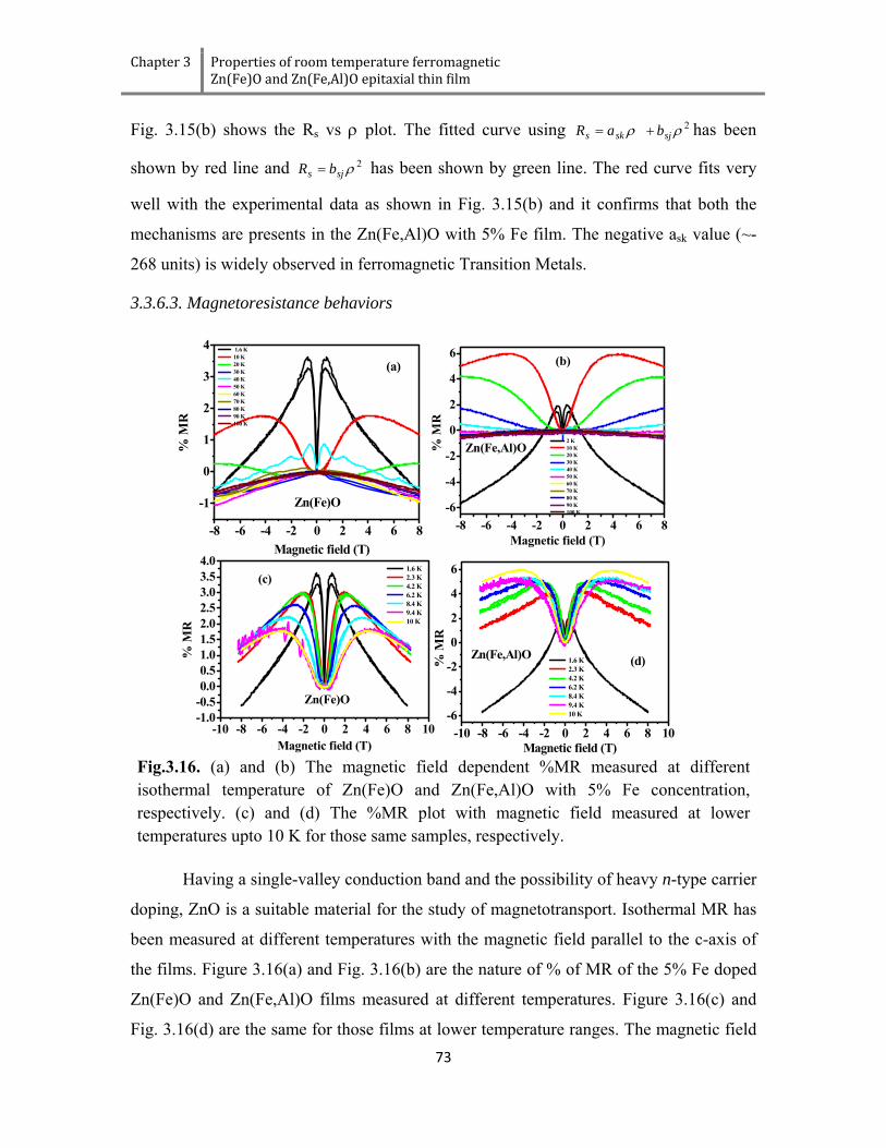
Chapter 3 Properties of room temperature ferromagnetic Zn(Fe)O and Zn(Fe,Al)O epitaxial thin film
73
Fig. 3.15(b) shows the Rs vs ρ plot. The fitted curve using 2ρρ sjsks baR += has been
shown by red line and 2ρsjs bR = has been shown by green line. The red curve fits very
well with the experimental data as shown in Fig. 3.15(b) and it confirms that both the
mechanisms are presents in the Zn(Fe,Al)O with 5% Fe film. The negative ask value (~-
268 units) is widely observed in ferromagnetic Transition Metals.
3.3.6.3. Magnetoresistance behaviors
Having a single-valley conduction band and the possibility of heavy n-type carrier
doping, ZnO is a suitable material for the study of magnetotransport. Isothermal MR has
been measured at different temperatures with the magnetic field parallel to the c-axis of
the films. Figure 3.16(a) and Fig. 3.16(b) are the nature of % of MR of the 5% Fe doped
Zn(Fe)O and Zn(Fe,Al)O films measured at different temperatures. Figure 3.16(c) and
Fig. 3.16(d) are the same for those films at lower temperature ranges. The magnetic field
-8 -6 -4 -2 0 2 4 6 8
-1
0
1
2
3
4 1.6 K 10 K 20 K 30 K 40 K 50 K 60 K 70 K 80 K 90 K 100 K
% M
R
Magnetic field (T)
(a)
Zn(Fe)O
-8 -6 -4 -2 0 2 4 6 8-6
-4
-2
0
2
4
6
2 K 10 K 20 K 30 K 40 K 50 K 60 K 70 K 80 K 90 K 100 K
% M
R
Magnetic field (T)
(b)
Zn(Fe,Al)O
-10 -8 -6 -4 -2 0 2 4 6 8 10-1.0-0.50.00.51.01.52.02.53.03.54.0
% M
R
Magnetic field (T)
1.6 K 2.3 K 4.2 K 6.2 K 8.4 K 9.4 K 10 K
Zn(Fe)O
(c)
-10 -8 -6 -4 -2 0 2 4 6 8 10-6
-4
-2
0
2
4
6
% M
R
Magnetic field (T)
1.6 K 2.3 K 4.2 K 6.2 K 8.4 K 9.4 K 10 K
Zn(Fe,Al)O (d)
Fig.3.16. (a) and (b) The magnetic field dependent %MR measured at different isothermal temperature of Zn(Fe)O and Zn(Fe,Al)O with 5% Fe concentration, respectively. (c) and (d) The %MR plot with magnetic field measured at lower temperatures upto 10 K for those same samples, respectively.

Properties of room temperature ferromagnetic Zn(Fe)O and Zn(Fe,Al)O epitaxial thin film
Chapter 3
74
dependent % of MR plot shows different behavior at different temperatures for all the
doped films as shown in Fig. 3.17.
The magnetoresistance (MR) of the films have been measured at different temperatures to
investigate the s–d exchange interaction between the conducting s-electron spins and the
d-electron spins localized at the magnetic Fe impurities [55]. We have observed the
positive MR at low magnetic field and negative MR at higher magnetic field. The s-d
exchange-induced spin splitting of the conduction band could account for positive MR
while suppression of electrons at weak localization of impurity centers could account for
the negative MR of the iron doped ZnO films. The behavior of MR at different field
range can be described in different four ways (i) A positive MR at lower field range
which arises in a two-band model from the action of the Lorentz force on the mobile
carriers. For carriers in closed orbits, this term is of the form 22
2%
cHbaHMR+
= . This
Fig. 3.17. %MR plot with magnetic field of Zn(Fe)O and Zn(Fe,Al)O thin films with different Fe concentrations. (a), (c) and (e) are the %MR nature of Zn(Fe)O thin films with different Fe concentrations at temperatures 1.6 K, 10 K and 20 K, respectively and (b), (d) and (f) are the %MR nature of Zn(Fe,Al)O samples at temperatures 1.6 K, 10 K and 20 K, respectively.

Chapter 3 Properties of room temperature ferromagnetic Zn(Fe)O and Zn(Fe,Al)O epitaxial thin film
75
saturates MR at higher fields, (ii) the open orbits terms, for which the magnetoresistance
is quadratic and nonsaturating, is 2% dHMR = , (iii) A negative term arises due to spin-flip
scattering from singly occupied localized states with s =1/2 which is given by
1cosh%1
−⎟⎟⎠
⎞⎜⎜⎝
⎛=
−
fHMR , (iv) A negative term due to scattering from a paramagnetic or
ferromagnetic moment is given by 2% hMMR = where h is the dimensionless coefficient
which depends on the strength of the s-d scattering in the system. The parameters a, b, c,
d, f and h are the constants depend on the free carrier concentrations, magnetic properties
of the films etc.
The %MR is strongly temperature as well as free carrier concentration dependent.
The semiconducting transition metal doped ZnO films show low field positive %MR at
1.6 K as shown in Fig. 3.17(a) and (b). Increasing of carrier concentration by
incorporating 1% Al causes decrease of low field positive MR and increase of high field
negative MR in the films. MR is positive at 10 K as shown in Fig. 3.17(c) and (d). The
enhanced positive MR in the Al incorporated systems is caused by enhanced spin
splitting of conduction band due to s-d exchange interactions. At 20 K the MR is negative
at lower field and positive at higher field as shown in Fig. 3.17(e) and (f). MR shows
oscillatory behavior at that temperature. The negative MR decreases in the Al
incorporated films due to enhancement of spin splitting conduction band. The films show
Fig.3.18. The plot of %MR measured at 8 T magnetic field with temperatures of Zn(Fe)O and Zn(Fe,Al)O thin films with 5% Fe. Inset (a) and (b) are the same plot for 7% and 10% Fe doped films, respectively.
0 20 40 60 80 100
-6
-4
-2
0
2
4
6
Zn(FeO) Zn(Fe,Al)O
%M
R a
t 8 T
Temperature (K)
5%
0 20 40 60 80 100-2
-1
0
1
2
3
% M
R a
t 8 T
Temperature (K)
7%
0 20 40 60 80 100-0.9
0.0
0.9
%M
R a
t 8 T
Temperature (K)
10%
(a)
(b)

Properties of room temperature ferromagnetic Zn(Fe)O and Zn(Fe,Al)O epitaxial thin film
Chapter 3
76
negligible negative MR over 50 K as the insulating type DMS films shows. The
temperature dependent %MR has been shown in Fig. 3.18 for Zn(Fe)O and Zn(Fe,Al)O
films with 5% Fe. The insets (a) and (b) of Fig. 3.18 are the same plot for 7 and 10% Fe.
As temperature increases the resistivity due to spin disorder scattering increases and it
becomes larger than the resistivities due to impurity and thermal scattering. So, the MR
increases with increasing temperature. At higher temperature the MR starts decreasing
because of the both ionized impurity scattering and phonon scattering become
independent of sub-band spin spilt energy (δ), whereas spin-disordered scattering
decreases with δ. So, the MR vs. temperature curve shows the hump giving a peak of MR
at a certain temperature.
3.4. Summary
The high crystalline quality epitaxial Zn(Fe)O thin film doped with iron deposited
on sapphire substrate at a substrate temperature of 450 ºC shows room temperature
ferromagnetic behavior. Increasing of Fe doping concentration in the ZnO films
decreases the magnetic moment of the systems. The incorporation of 1% Al enhances the
saturation moment up to three times for 5% Fe doped samples. This result concludes that
there is the effect of free carrier density on magnetism. A clear correlation between the
magnetization per transition metal ion and the ratio of the number of carriers and number
of donors have been found in these films and establishes the theory of carrier induced
ferromagnetism. From the detailed low temperature magnetization investigation of all our
(Fe,Al) doped films it has been confirmed that the ferromagnetic moment along with a
huge paramagnetic components are present in each film. The steep exponential rise of
ferromagnetic moment and paramagnetic susceptibility of the films in the lower
temperature regimes do not follow the standard Curie law but it behaves more like to a
insulating type DMS. We have also attempted to establish the carrier induced effect in
our DMS films using defect model.
The magnetic and transport properties of the Zn(Fe)O and Zn(Fe,Al)O films with
5, 7 and 10% Fe concentration grown by a PLD technique are investigated. Temperature-
dependent Hall effect measurements have been performed on Zn(Fe)O and Zn(Fe,Al)O
highly crystalline epitaxial thin films. We have extracted the free carrier concentration

Chapter 3 Properties of room temperature ferromagnetic Zn(Fe)O and Zn(Fe,Al)O epitaxial thin film
77
and Hall mobility using the ordinary Hall coefficient. The Hall data analysis revealed
that the dominant donor has an activation energy ranging from 33 to 41 meV. The
temperature dependent Hall mobility data has can be explained by several type of
scattering mechanism viz. ionized impurity, acoustic deformation, piezoelectric potential,
polar optical scattering and as well as grain boundary scattering. The high field saturating
nature of Hall resistivity in Zn(Fe,Al)O thin film also confirms the presence of
ferromagnetism in the film. The behavior of anomalous Hall co-efficient with linear film
resistivity confirms the presence of both scattering mechanisms (skew scattering and side
jump mechanism) in the Zn(Fe,Al)O epitaxial thin film. We have observed the positive
MR at low magnetic field and negative MR at higher magnetic field for all the doped
DMS fims. The s-d exchange-induced spin splitting of the conduction band could account
for positive MR while suppression of electron at weak localization of impurity centers
could account for the negative MR of the iron doped ZnO. Negative magnetoresistance at
higher magnetic field has been observed in transition-metal-doped ZnO DMS films at
lower temperature.
References
[1] T. Dietl, H. Ohno, F. Matsukura, J. Cibert, and D. Ferrand, Zener Model Description of Ferromagnetism in Zinc-Blende Magnetic Semiconductors, Science 287, 1019 (2000). [2] T. Story, R. R. Galazka, R. B. Frankel, and P. A. Wolff, Carrier-Concentration-Induced Ferromagnetism in PbSnMnTe, Phys. Rev. Lett. 56, 777 (1986). [3] P. Łazarczyk, T. Story, M. Arciszewska, and R. R. Gazka, Magnetic phase diagram of Pb1−x−ySnyMnxTe semimagnetic semiconductors J. Magn. Magn. Mater. 169, 151 (1997). [4] F. Matskura, H. Ohno, A. Shen, and Y. Sugawara, Transport properties and origin of ferromagnetism in GaMnAs, Phys. Rev. B 57, R2037 (1998). [5] H. Ohno, Making Nonmagnetic Semiconductors Ferromagnetic, Science 281, 951 (1998). [6] M. Oestreich, J. Hubner, D. Hagele, P. J. Klar, W. Heimbrodt, W. W. Ruhle, D. E. Ashenford, and B. Lunn, Spin injection into semiconductors, Appl. Phys. Lett. 74, 1251 (1999). [7] Y. Ohno, D. K. Young, B. Beschoten, F. Matskura, H. Ohno, and D. D. Awschalom, Electrical spin injection in a ferromagnetic semiconductor heterostructure, Nature 402, 790 (1999). [8] A. Kaminski, S. Das Sarma, Polaron Percolation in Diluted Magnetic Semiconductors, Phys. Rev. Lett. 88, 247202 (2002). [9] S. J. Pearton, C. R. Abernathy, M. E. Overberg, G. T. Thalei, D. P. Norton, N. Theodoropoulou, A. F. Hebard, Y. D. Park, F. Ren, J. Kim, and L. A. Boatner, Wide band gap ferromagnetic semiconductors and oxides, J. Appl. Phys. 93, 1 (2003).

Properties of room temperature ferromagnetic Zn(Fe)O and Zn(Fe,Al)O epitaxial thin film
Chapter 3
78
[10] S. Das Sarma, E. H. Hwang, and A. Kaminski, Temperature-dependent magnetization in diluted magnetic semiconductors, Phys. Rev. B 67, 155201 (2003). [11] A. Tiwari, M. Snure, D. Kumar, and J. T. Abiade, Ferromagnetism in Cu-doped ZnO films: Role of charge carriers, Appl. Phys. Lett. 92, 062509 (2008). [12] X. H. Xu, H. J. Blythe, M. Ziese, A. J. Behan, J. R. Neal, A. Mokhtari, R. M. Ibrahim, A. M. Fox, and G. A. Gehring, Carrier-induced ferromagnetism in n-type ZnMnAlO and ZnCoAlO thin films at room temperature, New J. Phys. 8, 135 (2006). [13] D. Karmakar, S. K. Mandal, R. M. Kadam, P. L. Paulose, A. K. Rajarajan, T. K. Nath, A. K. Das, I. Dasgupta, and G.P. Das, Ferromagnetism in Fe-doped ZnO nanocrystals: Experiment and theory, Phys. Rev. B 75, 144404 (2007). [14] A. J. Behan, A. Mokhtari, H. J. Blythe, D. Score, X. -H. Xu, J. R. Neal, A. M. Fox, and G. A. Gehring, Two Magnetic Regimes in Doped ZnO Corresponding to a Dilute Magnetic Semiconductor and a Dilute Magnetic Insulator, Phys. Rev. Lett. 100, 047206 (2008). [15] A. Singh, A. Dutta, S. K. Das, V. A. Singh, Generalized RKKY interaction and spin-wave excitations Ferromagnetism in a dilute magnetic semiconductor, Phys. Rev. B 68, 235208 (2003); S. Pandey, A. Singh, /arXiv:cond-mat/0502085v1S (2005). [16] M. Kobayashi, Y. Ishida, J. l. Hwang, T. Mizokawa, A. Fujimori, K. Mamiya, J. Okamoto, Y. Takeda, T. Okane, Y. Saitoh, Y. Muramatsu, A. Tanaka, H. Saeki, H. Tabata, and T. Kawai, Characterization of magnetic components in the diluted magnetic semiconductor Zn1−xCoxO by x-ray magnetic circular dichroism, Phys. Rev. B 72, 201201(R) (2005). [17] H. Hori, S. Sonoda, T. Sasaki, Y. Yamamoto, S. Shimizu, K. I. Suga, and K. Kindo, High-TC ferromagnetism in diluted magnetic semiconducting GaN:Mn films, Physica B 324, 142 (2002). [18] J. H. Yang, L. Y. Zhao, Y. J. Zhang, Y. X.Wang, and H. L. Liu, Paramagnetic behavior of Zn1−xMnxO at room temperature, Cryst. Res. Technol. 43, 999 (2008). [19] D. W. Hamby, D. A. Lucca, M. J. Klopfstein, and G. J. Cantwell, Temperature dependent exciton photoluminescence of bulk ZnO, J. Appl. Phys. 93, 3214 (2002). [20] D. L. Hou, R. B. Zhao, Y. Y. Wei, C. M. Zhen, C. F. Panand, and G. D. Tang, Room temperature ferromagnetism in Ni-doped ZnO films, Curr. Appl. Phys. 10, 124 (2010). [21] W. B. Mi, H. L. Bai, H. Liu, and C. Q. Sun, Microstructure, magnetic, and optical properties of sputtered Mn-doped ZnO films with high-temperature ferromagnetism, J. Appl. Phys. 101, 023904 (2007). [22] S. Das Sarma, E.H. Hwang, and A. Kaminski, Temperature-dependent magnetization in diluted magnetic semiconductors, Phys. Rev. B 67, 155201 (2003). [23] K. H. J. Buschow, and F. R. de Boer, Physics of Magnetism and Magnetic Materials, Kluwer Academic Publishers, New York, Boston, Dordrecht, London, Moscow (2003). [24] X. Li, Z. Yu, X. Long, P. Lin, X. Cheng, Y. Liu, C. Cao, H. Zhang, G.Wu, and R. Yu, Synthesis and magnetic properties of Al doped Zn0.995Mn0.005O powers, Appl. Phys. Lett. 94, 252501 (2009). [25] J. M. D. Coey, M. Venkatesan, and C. B. Fitzgerald, Donor impurity band exchange in dilute ferromagnetic oxides, Nature Mater. 4, 173 (2005). [26] Z. Jin, T. Fukumura, M. Kawasaki, K. Ando, H. Saito, T. Sekiguchi, Y. Z. Yoo, M. Murakami, Y. Matsumoto, T. Hasegawa, and H. Koinuma, High throughput fabrication

Chapter 3 Properties of room temperature ferromagnetic Zn(Fe)O and Zn(Fe,Al)O epitaxial thin film
79
of transition-metal-doped epitaxial ZnO thin films: A series of oxide-diluted magnetic semiconductors and their properties, Appl. Phys. Lett. 78, 3824 (2001). [27] T. Andrearczyk, J. Jaroszyński G. Grabecki, T. Dietl, T. Fukumura, and M. Kawasaki, Spin-related magnetoresistance of n-type ZnO:Al and Zn1−xMnxO:Al thin films, Phys. Rev. B 72, 121309R (2005). [28] W. Shim, K. Lee, W. Lee, K. A. Jeon, and S. Y. Lee, Myung H. Jung, Evidence for carrier-induced ferromagnetic ordering in Zn1−xMnxO thin films: Anomalous Hall effect, J. Appl. Phys. 101, 123908 (2007). [29] J. S. Higgins, S. R. Shinde, S. B. Ogale, T. Venkatesan, and R. L. Greene, Hall effect in cobalt-doped TiO2, Phys. Rev. B 69, 073201 (2004). [30] Qingyu Xu, Lars Hartmann, Heidemarie Schmidt, Holger Hochmuth, Michael Lorenz, Annette Setzer, Pablo Esquinazi, Christoph Meinecke, and Marius Grundmann, Magnetotransport properties of Zn90Mn7.5Cu2.5O100 films, Thin Solid Films 516, 1160 (2008). [31] Hidemi Toyosaki, Tomoteru Fukumura, Yasuhiro Yamada, Kiyomi Nakajima, Toyohiro Chikyow, Tetsuya Hasegawa, Hideomi Koinuma, Masashi Kawasaki, Anomalous Hall effect governed by electron doping in a room-temperature transparent ferromagnetic semiconductor, Nature 3, 221 (2004). [32] Ncholu Manyala, Yvan Sidis, John F. DiTusa, Gabriel Aeppli, David P. Young, Zachary Fisk, Large anomalous Hall effect in a silicon-based magnetic semiconductor, Nature 3, 255 (2004). [33] Robert Karplus and J. M. Luttinger, Hall Effect in Ferromagnetics, Phy. Rev. 95 1154 (1954). [34] J. Smit, The spontaneous hall effect in ferromagnetics II, Physica 24, 39 (1958) [35] L. Burger, Side-Jump mechanism for the Hall Effect of Ferromagnets, Phys. Rev. B, 2, 4559 (1970). [36] Zhong Fang, Naoto Nagaosa, Kei S. Takahashi, Atsushi Asamitsu, Roland Mathieu, Takeshi Ogasawara, Hiroyuki Yamada, Masashi Kawasaki, Yoshinori Tokura, and Kiyoyuki Terakura, The Anomalous Hall Effect and Magnetic Monopoles in Momentum Space, Science 302, 92 (2003). [37] Y. D. Park, A. Wilson, A. T. Hanbicki, J. E. Mattson, T. Ambrose, G. Spanos, and B. T. Jonker, Magnetoresistance of Mn:Ge ferromagnetic nanoclusters in a diluted magnetic semiconductor matrix, Appl. Phys. Lett. 78, 2739 (2001) [38] T. Hayashi, M. Tanaka, and T. Nishinaga, H. Shimada, Magnetic and magnetotransport properties of new III-V diluted magnetic semiconductors: GaMnAs, J. Appl. Phys. 81, 4865 (1997). [39] M. Venkatesan, P. Stamenov, L. S. Dorneles, R. D. Gunning, B. Bernoux, and J. M. D. Coey, Magnetic, magnetotransport, and optical properties of Al-doped Zn0.95Co0.05O thin films, Appl. Phys. Lett. 90, 242508 (2007). [40] Sayak Ghoshal and P S Anil Kumar, Suppression of the magnetic moment upon Co doping in ZnO thin film with an intrinsic magnetic moment, J. Phys.: Cond. Mat. 20, 192201 (2008). [41] Y. Fukuma, F. Odawara, H. Asada, and T. Koyanagi, F. Odawara, H. Asada, and T. Koyanagi Effects of annealing and chemical doping on magnetic properties in Co-doped ZnO films, Phys. Rev. B 78, 104417 (2008).
Properties of room temperature ferromagnetic Zn(Fe)O and Zn(Fe,Al)O epitaxial thin film
Chapter 3
80
[42] Qingyu Xu, Lars Hartmann, Heidemarie Schmidt, Holger Hochmuth, Michael Lorenz, Rüdiger Schmidt-Grund, Chris Sturm, Daniel Spemann, and Marius Grundmann, Metal-insulator transition in Co-doped ZnO: Magnetotransport properties, Phys. Rev. B 73, 205342 (2006). [43] S. S. P. Parkin, N. More, and K. P. Roche, Oscillations in exchange coupling and magnetoresistance in metallic superlattice structures: Co/Ru, Co/Cr, and Fe/Cr, Phys. Rev. Lett. 64, 2304 (1990). [44] Jagadeesh S. Moodera, Janusz Nowak, and Rene J. M. van de Veerdonk, Interface Magnetism and Spin Wave Scattering in Ferromagnet-Insulator-Ferromagnet Tunnel Junction, Phys. Rev. Lett. 80, 2941 (1998). [45] T. Ditel, J. Spalek, Effect of thermodynamic fluctuations of magnetization on the bound magnetic polaron in dilute magnetic semiconductors, Phys. Rev. Lett. 28, 1548 (1983). [46] Jing Wang, Zhengbin Gu, Minghui Lu, Di Wu, Changsheng Yuan, Shantao Zhang, Yanfeng Chen, Shining Zhu, and Yongyuan Zhu, Giant magnetoresistance in transition-metal-doped ZnO films, Appl. Phys. Lett. 88, 252110 (2006). [47] K T Roro, G H Kassier, J K Dangbegnon, S Sivaraya, J E Westraadt, J H Neethling, A W R Leitch and J R Botha, Temperature-dependent Hall effect studies of ZnO thin films grown by metalorganic chemical vapour deposition, Semicond. Sci. Technol. 23, 055021 (2008). [48] P. P. Debye and E. M. Conwell, Electrical Properties of N-Type Germanium, Phys. Rev. 93, 693(1954). [49] J. M. Dorkel, P. Leturcq, Carrier mobilities in silicon semi-empirically related to temperature, doping and injection level, Solid State Electronics 24, 821 (1981). [50] Seong-Il Kim, Chang-Sik Son, Min-Suk Lee, Yong Kim, Moo-Sung Kim, and Suk-Ki Min, Temperature dependent electrical properties of heavily carbon-doped GaAs grown by low-pressure metalorganic chemical vapor deposition, Solid State Comm. 93, 939 (1995). [51] Y. Z. Peng, T. Liew, T. C. Chong, C. W. An, and W. D. Song, Anomalous Hall effect and origin of magnetism in Zn1−xCoxO thin films at low Co content, Appl. Phys. Lett. 88, 192110 (2006). [52] Qingyu Xu, Lars Hartmann, Heidemarie Schmidt, Holger Hochmuth, Michael Lorenz, Rüdiger Schmidt-Grund, Daniel Spemann, and Marius Grundmann, Magnetoresistance effects in Zn0.90Co0.10O films, J. Appl. Phys. 100, 013904 (2006). [53] P. Khatua, T. K. Nath, and A. K. Majumdar, Extraordinary Hall effect in self-assembled epitaxial Ni nanocrystallites embedded in a TiN matrix, Phys. Rev. B 73, 064408 (2006). [54] Z. Yang, W. P. Beyermann, M. B. Katz, O. K. Ezekoye, Z. Zuo, Y. Pu, J. Shi, X. Q. Pan, and J. L. Liu, Microstructure and transport properties of ZnO:Mn diluted magnetic semiconductor thin films, J. Appl. Phys. 105, 053708 (2009). [55] P. Stamenov, M. Venkatesan, and L. S. Dorneles, D. Maude, and J. M. D. Coey, Magnetoresistance of Co-doped ZnO thin films, J. Appl. Phys. 99, 08M124 (2006).

Chapter 4
Junction magnetoresistance of Pt/Zn(Fe)O and
Pt/Zn(Fe,Al)O metal-dilute magnetic semiconductor
junction
This chapter is based on
International journal 1. Room temperature enhanced positive magnetoresistance in Pt and carrier induced Zn(Fe)O and Zn(Fe,Al)O
dilute magnetic semiconductor junction) by S. Chattopadhyay, T. K. Nath Journal of Applied Physics vol. 108, pp. 083904 (2010). Selected for Virtual Journal of Nanoscale Science & Technology for the October 25, (2010)
Conference/Symposia 2. Room temperature magnetic sensors with Zn(FeAl)O by Pt Schottky contact by S. Chattopadhyay, T. K. Nath
54th DAE Solid State Physics Symposium (2009)

Junction magnetoresistance of Pt/Zn(Fe)O and Pt/Zn(Fe,Al)O metal‐dilute magnetic semiconductorjunction
Chapter 4
81
4.1. Introduction
Spin-polarized electron injection into semiconductors has been a field of growing
interest in present microelectronics era. The injection and detection of a spin-polarized
current in a semiconducting material could combine magnetic storage of information with
electronic readout in a single semiconductor device [1]. Spin injection across a
ferromagnet-nonmagnetic metal interface provided a cornerstone for the field of spin
dependent transport in metals. The spin degree of freedom holds promise for the
realization of enhanced or novel device concepts and applications in microelectronics.
Most of the existing spintronic applications are based on metallic devices such as spin
valves [2], magnetic tunnel junctions [3], spin torque effects [4], domain wall devices [5],
etc. An important hurdle in this context is the inefficient injection of spin-polarized
currents from metallic ferromagnets into semiconductors due to the large mismatch in
conductivities [6]. Another research direction is the study of spin injection and transport
in more traditional devices aimed at room-temperature operation [7].
Zinc oxide based materials have many interesting and useful properties in the
field of optoelectronics and sensing devices [8,9]. Applications of such materials are
especially attractive on consideration of the low cost and lack of toxicity of zinc oxide.
The investigation on diluted magnetic semiconductors (DMS) [10-13] demonstrated an
application of ZnO as a host material for spintronic devices, which make use of electron
spin for data reading and writing. To integrate the DMS into present electronics, low-
dimensional structures are required for exploiting the advantages offered by the spin [14].
The basic DMS property of ZnO is that it shows ferromagnetism at room temperature.
In this chapter, the room temperature J-V properties of the junction between
paramagnetic novel metal, Pt and dilute magnetic semiconductor with 5, 7 and 10% iron
doped ZnO have been studied. In this work we have showed that the reasonably high
value of positive magnetoresistances persists at the junction at room temperature and it
depends on the magnitude of the magnetic moment of the dilute magnetic
semiconducting (DMS) ZnO films.
4.2. Experimental procedure
The detailed preparation method of the pulsed laser deposited iron doped epitaxial
ZnO thin films [Zn(Fe)O] and 1% Aluminum incorporated iron doped ZnO films

Chapter 4 Junction magnetoresistance in Pt and carrier induced Zn(Fe)O and Zn(Fe,Al)O junction
82
[Zn(Fe,Al)O] with iron concentrations 5, 7, 10% have been discussed in chapter-3
section-3.2. The point contact Pt metal has been used with the film to make a non-ohmic
(Schottky) type contact. Undoped ZnO thin film has also been grown on c-plane (0001)
sapphire substrate using the same PLD technique employing KrF excimer laser (λ = 248
nm) as discussed in chapter-3 for comparative study.
The I-V characterizations have been carried out using Keithley 2612 source meter
with 1 microvolt resolution. The magnetic field was applied in the direction of current
parallel to the film plane geometry using a high precision electromagnet (polytronic,
model HEM 100).
4.3. Results and discussion
4.3.1. Structural properties
The cross sectional high resolution transmission electron microscope (HRTEM)
image, shown in Fig. 4.1(a) clearly establishes that the ZnO films grown on (0001)
sapphire substrate are highly epitaxial and well crystalline in nature. The film - substrate
interface is very sharp having extremely good lattice matching between substrate and film
as discussed detailed in chapter-3.
(b)(a)
(c) (d)
Fig.4.1. (a) Cross sectional HRTEM image of Zn(Fe)O on sapphire substrate confirms that the films are epitaxial and well crystalline in nature. (b) Room temperature near edges EXAFS spectra for both Zn(Fe)O and Zn(Fe,Al)O epitaxial films compared to some standards. The valence looks to be Fe2+ for both the ZnO films. (c) and (d) are the AFM image of Zn(Fe)O for the scan area of 5 μm × 5 μm and 1 μm × 1 μm, respectively.
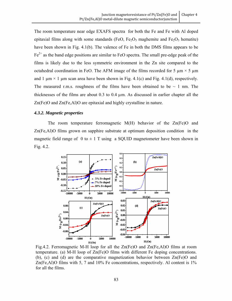
Junction magnetoresistance of Pt/Zn(Fe)O and Pt/Zn(Fe,Al)O metal‐dilute magnetic semiconductorjunction
Chapter 4
83
The room temperature near edge EXAFS spectra for both the Fe and Fe with Al doped
epitaxial films along with some standards (FeO, Fe2O3 maghemite and Fe2O3 hematite)
have been shown in Fig. 4.1(b). The valence of Fe in both the DMS films appears to be
Fe2+ as the band edge positions are similar to FeO spectra. The small pre-edge peak of the
films is likely due to the less symmetric environment in the Zn site compared to the
octahedral coordination in FeO. The AFM image of the films recorded for 5 µm × 5 µm
and 1 µm × 1 µm scan area have been shown in Fig. 4.1(c) and Fig. 4.1(d), respectively.
The measured r.m.s. roughness of the films have been obtained to be ~ 1 nm. The
thicknesses of the films are about 0.3 to 0.4 μm. As discussed in earlier chapter all the
Zn(Fe)O and Zn(Fe,Al)O are epitaxial and highly crystalline in nature.
4.3.2. Magnetic properties
The room temperature ferromagnetic M(H) behavior of the Zn(Fe)O and
Zn(Fe,Al)O films grown on sapphire substrate at optimum deposition condition in the
magnetic field range of 0 to ± 1 T using a SQUID magnetometer have been shown in
Fig. 4.2.
-10000 -5000 0 5000 10000-0.4
-0.3
-0.2
-0.1
0.0
0.1
0.2
0.3
0.4
Zn(Fe)O
Zn(FeAl)O
H (Oe)
M (μ
B/F
e2+ )
(b)
-10000 -5000 0 5000 10000-0.15
-0.10
-0.05
0.00
0.05
0.10
0.15
5% Fe doped 7% Fe doped 10% Fe doped
M (μ
B/F
e2+ )
H (Oe)
(a)
-10000 -5000 0 5000 10000
-0.08
-0.04
0.00
0.04
0.08
Zn(Fe)O
Zn(FeAl)O
M (μ
B/F
e2+ )
H (Oe)
(c)
-10000 -5000 0 5000 10000-0.04
-0.03-0.02
-0.010.000.01
0.020.03
Zn(Fe)O
Zn(FeAl)O
H (Oe)
M (μ
B/F
e2+ )
(d)
Fig.4.2. Ferromagnetic M-H loop for all the Zn(Fe)O and Zn(Fe,Al)O films at room temperature. (a) M-H loop of Zn(Fe)O films with different Fe doping concentrations. (b), (c) and (d) are the comparative magnetization behavior between Zn(Fe)O and Zn(Fe,Al)O films with 5, 7 and 10% Fe concentrations, respectively. Al content is 1% for all the films.

Chapter 4 Junction magnetoresistance in Pt and carrier induced Zn(Fe)O and Zn(Fe,Al)O junction
84
The diamagnetic contributions of sapphire substrate have been subtracted carefully at
each magnetic field from the net magnetization (uncorrected raw data) to estimate the
actual ferromagnetic contribution of such ferromagnetic films at 300 K [Detailed work on
this is discussed in chapter-3]. Figure 4.2(a) shows the M-H loop of Zn(Fe)O samples
with different doping concentrations of iron. Figure 4.2(b), (c) and (d) show comparative
study of Zn(Fe)O and Zn(Fe,Al)O films with 5, 7 and 10% Fe doped, respectively. After
correcting the substrate contributions in SQUID raw data a ferromagnetic hysteretic
M(H) behavior at room temperature is observed for both kind films. The coercive field
and saturation magnetization for the Zn(Fe)O sample are found to be 135 Oe and 0.18
μB/Fe2+. In the case of 1% Al incorporated film the coercive field is 69 Oe and the
saturation magnetization is strikingly enhanced to 0.4 μB/Fe2+. The 7% and 10% Fe doped
Zn(Fe)O samples show magnetic moment 0.04 μB/Fe2+ and 0.02 μB/Fe2+ respectively.
The decrease of ferromagnetic moment with increasing concentration of iron may be due
to the increase of antiferromagnetic coupling between Fe pairs in the matrix. With
increase in the Fe doping in ZnO, the average distance between adjacent Fe2+ ions
reduces. As the antiferromagnetic energy is less than ferromagnetic energy, the
antiferromagnetic coupling between Fe2+⎯Fe2+ ions dominates at higher Fe
concentrations and act as a ferromagnetic moment killer reducing average magnetic
moment per Fe ion. Similar results are obtained for Mn doped and Ni doped ZnO films
[15,16]. 1% Al incorporation for those higher doping (7% and 10% Fe doping) cases also
enhances the magnetic moment mainly due to enhanced carrier induced ferromagnetism
[12].
4.3.3 Current-voltage characteristics without applied magnetic field
The current density-voltage (J-V) characteristics of Zn(Fe)O and Zn(Fe,Al)O with
Pt non-ohmic point contact with 0.28±0.01 mm2 contact area has been shown in Fig. 4.3.
Figure 4.3(a) shows the J-V behavior of Zn(Fe)O films with different Fe doping
percentages. Figure 4.3(b), (c) and (d) are the comparative J-V behavior of ZnO, Zn(Fe)O
and Zn(Fe,Al)O for 5%, 7% and 10% iron doping, respectively. The junction J-V
characteristics are denoted as [17],
⎟⎟⎠
⎞⎜⎜⎝
⎛ −=
kTIRVe
JJ s
η)(
exp0 (4.1)

Junction magnetoresistance of Pt/Zn(Fe)O and Pt/Zn(Fe,Al)O metal‐dilute magnetic semiconductorjunction
Chapter 4
85
where, J0 is the reverse saturation current density. η and Rs are, ideality factor and
junction series resistance, respectively. The parameters evaluated from the forward J-V
curves of all the films shown in Fig. 4.3 have been summarized in Table 4.1. The ideality
factor of all Zn(Fe,Al)O samples lies between 1 and 2 and the values are near to 1 implies
that the thermionic emission dominates in Zn(Fe,Al)O samples whereas for Zn(Fe)O
films recombination degeneration transport process along with other defect induced
transport mechanism dominates.
4.3.4. Current-voltage characteristics with applied magnetic field
Figure 4.4 shows the forward J-V characteristics of such magnetic
semiconducting thin film junctions with Pt point contact and the J-V behaviors show
reasonably high sensitivity under magnetic field according to their magnetic moments.
Figure 4.4(a), (b) and (c) are the J-V plot of Zn(Fe)O films with 5, 7 and 10% iron
-8 -6 -4 -2 0 2 4 6 810-4
10-3
10-2
10-1
100
101
(b)Cur
rent
den
sity
(A/c
m2 )
ZnO Zn(FeAl)O Zn(Fe)O
Voltage (V)
5% Fe doped
-8 -6 -4 -2 0 2 4 6 810-4
10-3
10-2
10-1
100
101
(c)
Cur
rent
den
sity
(A/c
m2 )
ZnO Zn(Fe)O Zn(FeAl)O
Voltage (V)
7% Fe doped
-8 -6 -4 -2 0 2 4 6 810-4
10-3
10-2
10-1
100
101
(d)
Cur
rent
den
sity
(A/c
m2 )
Voltage (V)
ZnO Zn(Fe)O Zn(FeAl)O
10% Fe doped
-8 -6 -4 -2 0 2 4 6 810-4
10-3
10-2
10-1
100
Cur
rent
den
sity
(A/c
m2 )
Voltage (V)
ZnO Zn(Fe)O 5% Fe Zn(Fe)O 7% Fe Zn(Fe)O 10% Fe
(a)
Fig. 4.3. Junction J-V characteristics for all the Zn(Fe)O and Zn(Fe,Al)O films at room temperature. (a) J-V characteristics of Zn(Fe)O films with different Fe doping concentrations. (b), (c) and (d) are the comparative J-V study between Zn(Fe)O and Zn(Fe,Al)O films with 5, 7 and 10% Fe concentrations, respectively. Al content is 1% for all films.

Chapter 4 Junction magnetoresistance in Pt and carrier induced Zn(Fe)O and Zn(Fe,Al)O junction
86
doping, respectively, and Fig. 4.4(d), (e) and (f) are the same plots of Zn(Fe,Al)O
samples. The change of junction magneto-resistances (JMR) at a fixed bias voltage (7 V)
with applied magnetic field up to 0.6 T of different Zn(Fe)O and Zn(Fe,Al)O have been
shown in corresponding insets of Fig. 4.4. The J-V characteristics under magnetic field
have been fitted by the Eq. (4.1) and the parameters have been summarized in Table 4.1.
The series resistance increases with applied magnetic field and it shows the positive
junction magneto-resistance behavior of the films.
-0.6 -0.3 0.0 0.3 0.6
0
2
4
6
8
10
0 1 2 3 4 5 6 7 80
2
4
6
8
10
12
% J
MR
Magnetic field (T)
(e)
Cur
rent
den
sity
(A/c
m2 )
0.6 T
0 T
Voltage (V)
Zn(FeAl)O with 7% Fe and1% Al
-0.6 -0.3 0.0 0.3 0.6
0
2
4
6
8
0 1 2 3 4 5 6 7 80
2
4
6
8
10
12
% J
MR
Magnetic field (T) (f)
Cur
rent
den
sity
(A/c
m2 )
0.6 T
0 T
Voltage (V)
Zn(FeAl)O with 10% Fe and 1% Al
0 2 4 6 80
2
4
6
8
10
12
-0.6 -0.3 0.0 0.3 0.6
0
5
10
15
20
(d)C
urre
nt d
ensi
ty (A
/cm
2 )
0.6 T
Voltage (V)
0T
Zn(FeAl)O with 5% Fe and 1% Al
% J
MR
Magnetic field (T)
0 2 4 6 8 100.0
0.5
1.0
1.5
2.0
2.5
3.0
3.5
-0.6 -0.3 0.0 0.3 0.6
0
2
4
6
8
(b)
Cur
rent
den
sity
(A/c
m2 )
0.6 T
Voltage (V)
Zn(Fe)O with 7% Fe
0 T
Magnetic field (T)
% J
MR
-0.6 -0.3 0.0 0.3 0.60
1
2
3
0 2 4 6 8 100.0
0.5
1.0
1.5
2.0
2.5
3.0
3.5
% J
MR
Magnetic field (T) (c)
Cur
rent
den
sity
(A/c
m2 )
0.6 T0 T
Voltage (V)
Zn(Fe)O with 10% Fe
0 2 4 6 8 100.0
0.5
1.0
1.5
2.0
2.5
3.0
3.5
-0.6 -0.3 0.0 0.3 0.6
0
2
4
6
8
10
Zn(Fe)O with 5% Fe
Cur
rent
den
sity
(A/c
m2 )
Voltage (V)
0.6 T
0 T
(a)
% JM
R
Magnetic field(T)
Fig. 4.4. Junction J-V characteristics with and without applied magnetic field at room temperature; (a), (b) and (c) are the J-V properties of Zn(Fe)O film with Fe concentration 5, 7 and 10%, respectively. (d), (e) and (f) are the same of Zn(Fe,Al)O with Fe concentration 5, 7 and 10%, respectively. Insets of all the figures of Fig.4 are the plot of %JMR with different applied magnetic field of the corresponding junctions. The blue lines are the corresponding fitted curves.

Junction magnetoresistance of Pt/Zn(Fe)O and Pt/Zn(Fe,Al)O metal‐dilute magnetic semiconductorjunction
Chapter 4
87
Table 4.1. Parameters extracted from the fitting of J-V characteristics
Applied
magnetic
field
Samples Reverse
saturation current
density (A/cm2)
Ideality factor Series
resistance
(Ω-cm)
0 T Zn(Fe)O with
5% Fe
0.025 6.89 2.67733
Zn(FeAl)O with
5% Fe
0.01429 1.12 0.61597
Zn(Fe)O with
7% Fe
0.04643 9.19 2.74142
Zn(FeAl)O with
7% Fe
0.01786 1.13 0.63501
Zn(Fe)O with
10% Fe
0.04643 9.19 2.82621
Zn(FeAl)O with
10% Fe
0.01429 1.13 0.66354
0.6 T Zn(Fe)O with
5% Fe
0.03929 10.72 2.81462
Zn(FeAl)O with
5% Fe
0.325 9.47 0.66514
Zn(Fe)O with
7% Fe
0.05714 12.54 2.7769
Zn(FeAl)O with
7% Fe
0.02143 2.51 0.68197
Zn(Fe)O with
10% Fe
0.04286 11.23 2.85482
Zn(FeAl)O with
10% Fe
0.03571 0.64 2.67733

Chapter 4 Junction magnetoresistance in Pt and carrier induced Zn(Fe)O and Zn(Fe,Al)O junction
88
4.3.5. Junction magneto-resistance properties
The increase of junction series resistance can be explained by the theoretical
model of spin tunneling in ferromagnetic to non-magnetic junctions [18]. The spin
injection process alters the potential drop across the F/N interface because differences of
spin dependent electrochemical potentials on either side of the interface generate an
effective resistance Rδ . It follows that 2/)0()0()0( sFFFnJ PJR μμμ σ+−= . R is the
junction series resistance, μn(0) and μF(0) are the electrochemical potentials for non-
magnetic and ferromagnetic sides of the junctions, J is the junction current density. PσF is
related to the conductivity polarization at the ferromagnetic interface and μsF(0) is the
spin accumulation at ferromagnetic side. Under magnetic field the junction series
resistance can be modified by RRR JJm δ+= where δR is the change of junction series
resistance and it can be expressed by,
( ) ( )
⎥⎥⎦
⎤
⎢⎢⎣
⎡ −++= ΣΣ
FN
FcFcFFN
rPPrrPrPrr
R222
σσδ (4.2)
where, rF, rN and rc are the ferromagnetic, non-ferromagnetic and contact resistance
respectively. ΣP is the contact conductivity polarization. rFN is the effective equilibrium
resistance of the Ferromagnetic/Non-ferromagnetic junction. From Eq. (4.2) it can be
clearly seen that the δR is always positive i.e. δR > 0 at higher applied potentials. The
positive junction MR and rectifying behavior has also been observed in ZnO
heterostructures with other ferromagnetic systems. Similar spin injection theory has been
evoked to explain their observed positive junction MR at the ferromagnet/semiconductor
interface [19,20].
The plot of % of junction MR (JMR) with applied magnetic field at a bias voltage
of 7 V has been shown in the insets of Fig. 4.4. It shows that the JMR behavior follows a
simple empirical relation with magnetic field as [21], βαHJMR= (4.3)
where, α and β are coefficients and are evaluated employing a non-linear least square
fitting using χ2 minimization technique. The coefficients thus obtained are listed in

Junction magnetoresistance of Pt/Zn(Fe)O and Pt/Zn(Fe,Al)O metal‐dilute magnetic semiconductorjunction
Chapter 4
89
Table- 4.2 for all the samples. The coefficient β is lower than one at room temperature
showing nonlinear magnetic field dependence of positive MR of the junction.
Table 4.2. Fit parameters α and β from junction magnetoresistance plot
Sample α (T- β) β
Zn(Fe)O with 5% Fe 0.13 0.56
Zn(Fe)O with 7% Fe 10.31 0.70
Zn(Fe)O with 10% Fe 4.21 0.63
Zn(FeAl)O with 5% Fe 30.39 0.83
Zn(FeAl)O with 7% Fe 12.90 0.63
Zn(FeAl)O with 10% Fe 10.81 0.51
The % of JMR is found to be strongly dependent on the magnetic moments of the
respective magnetic semiconducting films. From the magnetization as a function of the
carrier density (nc) obtained from room temperature Hall voltage measurements of all the
Zn(Fe)O and Zn(Fe,Al)O films with 5% iron, the maximum saturation magnetization
(Ms) at 300 K is observed for the films with optimized carrier density of nc/ni ≈ 0.4 as
shown in Fig. 4.5(a). The film growth conditions were changed systematically (varing
oxygen pressure, laser energy, and target to substrate distance etc.) optimizing the best
DMS film property. The localized spins of the Fe ions are interacting with band electrons
and the standard theory of DMS can be applied. The % of JMR of those films is observed
to follow interestingly the same trend as the magnetic moment of the films follows
[shown in Fig. 4.5(b)]. With increasing doping percentage of iron the magnetic moment
decreases. Fig. 4.5(c) shows the plot of magnetic moment as a function of doping
concentration. The drop of moment with increasing iron concentration may be due to the
increasing of antiferromagnetic coupling between Fe pairs which occurs at shorter
separation distances. The % of JMR also decreases with increasing doping concentration
mimicking the same trend as the magnetic moments of the DMS films demonstrate.

Chapter 4 Junction magnetoresistance in Pt and carrier induced Zn(Fe)O and Zn(Fe,Al)O junction
90
4.4. Summary
The room temperature ferromagnetic iron doped ZnO with Pt metal point contact
shows non-ohmic J-V behavior at room temperature and shows reasonably high
sensitivity under magnetic field. The Pt/Zn(Fe)O junction shows positive junction
magnetoresistance at room temperature and the phenomenon can be best explained using
usual ferromagnetic to paramagnetic spin injection theory. Incorporation of 1% Al shows
higher junction magnetoresistance compared to without Al doped films. The junction
magnetoresistances are found to strictly depend on the magnitude of magnetic moments
of the DMS films. The magnetic moment depends on the carrier density and also the JMR
depends on magnetic moment. As magnetic moment decreases due to higher
concentration of Fe, JMR also mimics the same behavior.
References
[1] P. R. Hammar, B. R. Bennett, M. J. Yang, and M. Johnson, Observation of Spin Injection at a Ferromagnet-Semiconductor Interface, Phys. Rev. Lett. 83, 203 (1999). [2] I. Appelbaum, D. J. Monsma, K. J. Russell, V. Narayanamurti, and C. M. Marcus, Spin-valve photodiode, Appl. Phys. Lett. 83, 3737 (2003).
0.0 5.0x10²⁰ 1.0x10²¹ 1.5x10²¹ 2.0x10²¹ 2.5x10²¹
8
10
12
14
16
18
20
% J
MR
Carrier concentration (cm-3)0 1x10²¹ 2x10²¹
0.00
0.05
0.10
0.15
0.20
0.25
0.30
0.35
0.40
M (m
B/F
e2+ )
Carrier concentration (cm-3)
5 6 7 8 9 102468
101214161820
Zn(Fe)O
Zn(Fe,Al)O
% J
MR
Fe doping percentage5 6 7 8 9 10
0.000.050.100.150.200.250.300.350.40
Zn(Fe)O
Fe doping percentage
M (μ
B/F
e2+ )
Zn(Fe,Al)O
(a) (b)
(c) (d)
Fig. 4.5. (a) Room temperature carrier induced ferromagnetism in Zn(Fe)O and Zn(Fe,Al)O films with Fe concentration 5%. (b) % JMR of the corresponding films. (c) Plot of magnetic moment with different doping concentrations of iron. (d) Corresponding JMR of those films at room temperature.

Junction magnetoresistance of Pt/Zn(Fe)O and Pt/Zn(Fe,Al)O metal‐dilute magnetic semiconductorjunction
Chapter 4
91
[3] A. Kalitsov, M. Chshiev, I. Theodonis, N. Kioussis, and W. H. Butler, Spin-transfer torque in magnetic tunnel junctions, Phys. Rev. B 79, 174416 (2009). [4] F. Junginger, M. Kläui, D. Backes, U. Rüdiger, T. Kasama, R. E. Dunin-Borkowski, L. J. Heyderman, C. A. F. Vaz, and J. A. C. Bland, Spin torque and heating effects in current-induced domain wall motion probed by transmission electron microscopy, Appl. Phys. Lett. 90, 132506 (2007). [5] D. A. Allwood, G. Xiong, C. C. Faulkner, D. Atkinson, D. Petit, and R. P. Cowburn, Magnetic Domain-Wall Logic, Science 309, 1688 (2005). [6] S. H. Chun, S. J. Potashnik, K. C. Ku, P. Schiffer, and N. Samarth, Spin-polarized tunneling in hybrid metal-semiconductor magnetic tunnel junctions, Phys. Rev. B 66, 100408 (2002). [7] W. Van Roy, P. Van Dorpe, R. Vanheertum, P. J. Vandormael, and G. Borgh, Spin Injection and Detection in Semiconductors—Electrical Issues and Device Aspect, IEEE Trans. Electron Devices 54, 933 (2007). [8] X. J. Zheng, B. Yang, T. Zhang, C. B. Jiang, S. X. Mao, Y. Q. Chen, and B. Yuan, Enhancement in ultraviolet optoelectronic performance of photoconductive semiconductor switch based on ZnO nanobelts film, Appl. Phys. Lett. 95, 221106 (2009) [9] S. W. Fan , A. K. Srivastava and V. P. Dravid, Nanopatterned polycrystalline ZnO for room temperature gas sensing, Sens. Act. B: Chem. 144, 159 (2010). [10] T. Dietl, H. Ohno, F. Matsukura, J. Cibert, and D. Ferrand , Zener Model Description of Ferromagnetism in Zinc-Blende Magnetic Semiconductors, Science 287, 1019 (2000). [11] X. J. Liu, X. Y. Zhu, C. Song, F. Zeng and F. Pan, Intrinsic and extrinsic origins of room temperature ferromagnetism in Ni-doped ZnO films, J. Phys. D: Appl. Phys. 42, 035004 (2009). [12] A. J. Behan, A. Mokhtari, H. J. Blythe, D. Score, X-H. Xu, J. R. Neal, A. M. Fox, and G. A. Gehring, Two Magnetic Regimes in Doped ZnO Corresponding to a Dilute Magnetic Semiconductor and a Dilute Magnetic Insulator, Phys. Rev. Lett. 100, 047206 (2008). [13] S. J. Pearton, C. R. Abernathy, M. E. Overberg, G. T. Thaler, D. P. Norton, N. Theodoropoulou, A. F. Hebard, Y. D. Park, F. Ren, J. Kim, and L. A. Boatner, Wide band gap ferromagnetic semiconductors and oxide, J. Appl. Phys. 93, 1 (2003) [14] C. Ronning, P. X. Gao, Y. Ding, Z. L. Wang, and D. Schwen, Manganese-doped ZnO nanobelts for spintronics, Appl. Phys. Lett. 84, 78 (2004). [15] D. L. Hou, R. B. Zhao, Y. Y. Wei, C. M. Zhen, C. F. Pan, G. D. Tang, Room temperature ferromagnetism in Ni-doped ZnO films, Curr. Appl. Phys. 10, 124 (2010) [16] W. B. Mi, H. L. Bai, Hui Liu, and C. Q. Sun, Microstructure, magnetic, and optical properties of sputtered Mn-doped ZnO films with high-temperature ferromagnetism, J. Appl. Phys. 101, 023904 (2007). [17] A. Singh, A Datta, S. K. Das, and V. A. Singh, Generalized RKKY interaction and spin-wave excitations Ferromagnetism in a dilute magnetic semiconductor, Phys. Rev. B 68, 235208 (2003). [18] S. J. May and B. W. Wessels, High-field magnetoresistance in p-InMnAs/n-InAs heterojunctions, Appl. Phys. Lett. 88, 072105 (2006).

Chapter 4 Junction magnetoresistance in Pt and carrier induced Zn(Fe)O and Zn(Fe,Al)O junction
92
[19] K. X. Jin, S. G. Zhao, C. L. Chen, J. Y. Wang, and B. C. Luo, Positive colossal magnetoresistance effect in ZnO/La0.7Sr0.3MnO3 heterostructure, Appl. Phys. Lett. 92, 112512 (2008). [20] S. Y. Park, Hyung Woo Lee, Young Soo Lee, D. F. Wang, Y. P. Lee and J. Y. Rhee, Magneto-transport properties of ZnO/La0.7Sr0.3MnO3 bilayer on p-Si(100), Phys. Stat. Sol. (c) 4, 4471 (2007). [21] T. Edahiro, N. Fujimura, and T. Ito, Formation of two-dimensional electron gas and the magnetotransport behavior of ZnMnO/ZnO heterostructure, J. Appl. Phys. 93,7673 (2003). [22] C. Song, X. J. Liu, F. Zeng, and F. Pan, Fully epitaxial ZnCoO/ZnO/ ZnCoO junction and its tunnel magnetoresistance, Appl. Phys. Lett. 91, 042106 (2007). [23] S. Honda, T. Ishikawa, K. Takai, Y. Mitarai, and H. Harad, New type magnetoresistance in Co/Si system, J. Magn. Magn. Mater. 290-291, 1063 (2005). [24] S. S. P. Parkin, C. Kaiser, A. Panchula, P. M. Rice, B. Hughes, M. Samant, and S. H. Yang, Giant tunnelling magnetoresistance at room temperature with MgO (100) tunnel barriers, Nature Mater. 3, 862 (2004). [25] J. Moser, M. Zenger, C. Gerl, D. Schuh, R. Meier, P. Chen, G. Bayreuther, W. Wegscheider, D. Weiss, C. H. Lai, R. T. Huang, M. Kosuth and H. Ebert, Bias dependent inversion of tunneling magnetoresistance in Fe/GaAs/Fe tunnel junctions, Appl. Phys. Lett. 89, 162106 (2006). [26] J. H. Hsua, S. Y Chen, W. M. Chang, C. R. Chang, Temperature dependence of magnetoresistance effect in Ag-Fe3O4 composites film, J. Magn. Magn. Mater. 272-276, 1772 (2004). [27] I. Žutić, J. Fabian and S. Das Sarma, Spintronics: Fundamentals and applications, Rev. Mod. Phys. 76, 323 (2004). [28] Z. G. Sheng, W. H. Song, Y. P. Sun, J. R. Sun, and B. G. Shen, Crossover from negative to positive magnetoresistance in La0.7Ce0.3MnO3-SrTiO3-Nb heterojunctions, Appl. Phys. Lett. 87, 032501 (2005).

Chapter 5
Structural, magnetic and electrical properties of
La0.7Sr0.3MnO3 thin films on p-Si
This chapter is based on
International journals 1. Low‐temperature resistivity minima in colossal magnetoresistive La0.7Sr0.3MnO3 thin film: A quantum
interference effect by S. Chattopadhyay and T. K. Nath, Solid state communications (Communicated)

Structural, magnetic and electrical properties of La0.7Sr0.3MnO3 thin films on p‐Si Chapter 5
93
5.1. Introduction
The perovskite manganites of the form R1-xAxMnO3 (R: rare earth elements, A: alkaline
earth elements) thin films have attracted much attention of the researchers due to its exceptional
electrical properties and the negative colossal magnetoresistance (CMR) effect [1-3]. The CMR
thin films have potential application in the field of the spintronics devices like magnetic field
sensor, hard disk read head and infrared bolometer. The large magnetoresistance (MR) ratio in
low magnetic field and at room temperature from the CMR materials have attracted much
attention in the area of research in manganites. There have been several reports on the La1-
xSrxMnO3 (LSMO) thin films [4-6] which attributes a high potential in application field.
The CMR effect and the correlated degrees of freedom of magnetic structure,
crystallographic structure and electrical resistivity in CMR materials, in addition to being of
fundamental scientific interest, appears to provide some scope for engineering in more sensitive
magnetoresistive response. The ‘colossal’ magnetoresistive (CMR) rare earth manganites display
a fascinating diversity of behaviors including several forms of magnetic, orbital and charge
ordering [7-9]. The materials also exhibit dramatic variations of physical properties with
frequency, temperature, chemical composition and applied strain, as well as the magnetoresistive
properties, which give them their colloquial name. The particular MR phenomena to be
described here are the massive decrease of resistance by application of a magnetic field [10-12].
The electronic inhomogeneities in the hole-doped La1-xSrxMnO3 have attracted considerable
attention with phase separation into conducting magnetic and insulating nonmagnetic domains
[13]. Among the La1-xSrxMnO3 families La0.7Sr0.3MnO3 shows the ferromagnetic behavior over
the room temperatures and a high value of magnetoresistance. Both the epitaxial and non-
epitaxial thin films of manganites show huge strain effects on their magnetic, electronic and
magneto-transport properties [14]. For device applications, it is necessary to find out the
properties of LSMO films on Si, as Si is widely used material in semiconductor industries. So, it
is necessary to find out the electrical and magnetic properties of the LSMO films with strain
effects. The defects in the crystal also affect the electrical and magneto-electrical properties and
hence it should be explored.
In this chapter, a detailed study of structural, magnetic, electrical, and magneto-electronic
properties of LSMO thin films have been explicitly studied. The effects of thickness and oxygen

Chapter 5 Structural, magnetic and electrical properties of La0.7Sr0.3MnO3 thin films on p‐Si
94
vacancy defects in the crystal have been elaborated and the dominating scattering process in the
conduction electron has been estimated.
5.2. Experimental procedure
5.2.1. Preparation of targets
The La0.7Sr0.3MnO3 powder have been synthesized through chemical pyrophoric reaction
process where we have employed stoichiometric mixtures of high purity La2O3 (99.99 %), SrCO3
(99.9+ %) and Mn(CH3COO)2 (99.0 %) [3]. After final grinding and pelletization of
La0.7Sr0.3MnO3 powders, the pelletized sample have been first heated at 800 °C for 12 h, then at
1000 °C for 12 h and at 1200 °C for another 12 h, with intermediate grinding. Final sintering of
the La0.7Sr0.3MnO3 target has been carried out at 1200 °C for 24 h.
5.2.2. Cleaning of substrates
La0.7Sr0.3MnO3 films on (100) p-Si substrate have been grown by Pulsed Laser Deposition
process using chemically synthesized single phase LSMO target. The substrates have been
cleaned in ultrasonic bath followed by chemical cleaning as mentioned below:
1. The p-Si (100) substrates have been first cleaned by de-ionized (DI) water in ultrasonic
chamber for 5 to 10 minutes to remove the dust particles.
2. Then the substrates have been cleaned ultrasonically for 5 to 10 minutes by acetone to
remove oils and greases over them.
3. Acetone has been cleaned using a high flow of DI water.
4. The mixture of NH4(OH), H2O2 and H2O with ratio 5:1:1 has been employed for substrate
cleaning to remove the acidic radicals and organic compounds. The substrates have been
kept in the solution till the end of reaction.
5. The substrates have been pulled out from the solution and cleaned using a high flow of DI
water.
6. Then the substrates have been kept in the mixture of H2O2 and H2SO4 (1:1) and boiled till
the boiling stops. It removes the basic radicals from the substrates and formed a SiO2 layer
over Si.
7. The substrates again cleaned using a high flow of DI water after removing it from the
solution.
8. Finally the oxide layers have been etched by dipping the substrate in 10 % HF solution.

Structural, magnetic and electrical properties of La0.7Sr0.3MnO3 thin films on p‐Si Chapter 5
95
Table 5.1: Condition for depositing different LSMO thin films on p-Si (100) substrates
Sample Name
Substrate treatment condition Film growth condition Sintering condition
T (ºC)
O2 pressure (mbar)
Oxidation time (min)
Final substrate Temp (ºC)
O2 pressure (mbar)
Deposition time (min)
Temp (ºC)
O2 pressure (mbar)
Sintering time (min)
Sample-1
800 10-5 No p-Si/SiO2 with native oxide 800 0.5 20 800 0.5 45
Sample-2
800 0.5 30 p-Si/SiO2 with thin oxide layer 800 0.5 20 800 0.5 45
Sample-3
800 0.5 45 p-Si/SiO2 with thick oxide layer 800 0.5 20 800 0.5 45
Sample-4
800 0.5 45 p-Si/SiO2 with thick oxide layer 800 5×10⁻³ 20 800 5×10⁻³ 45
Sample-5
800 0.5 45 p-Si/SiO2 with thick oxide layer 800 5×10⁻⁵ 20 800 5×10⁻⁵ 45
Sample-6
800 0.5 45 p-Si/SiO2 with thick oxide layer 800 0.5 15 800 0.5 45
Sample-7
800 0.5 45 p-Si/SiO2 with thick oxide layer 800 0.5 10 800 0.5 45

Chapter 5 Structural, magnetic and electrical properties of La0.7Sr0.3MnO3 thin films on p‐Si
96
5.2.3. Deposition of La0.7Sr0.3MnO3 film
The films have been deposited on (100) p-Si substrates employing the pulsed laser deposition
technique using 248 nm KrF excimer pulsed mode laser. The different substrate treatment
conditions and film growth conditions for different LSMO thin films has been summarized in
Table 5.1. The substrate to target distance has been kept at 4 cm and the repetition rate of pulsed
laser (~ 10 pulses/second) has been used for all the films.
The electrical contacts have been made with high purity Ag-paste on LSMO film. The
temperature dependent electronic- and magneto-transport measurements have been carried out
using a source meter (Keithley, model - 2612), current source (Keithley, model-6221), PID
temperature controller (Lakeshore, model-331). A cryogen free ± 8 T superconducting magnet
with VTI system down to temperature 2 K (Cryogenics, U.K.) has been employed for high field
and low temperature transport measurements of these LSMO thin films.
5.3. Results and discussion
5.3.1. Structural study
The high resolution x-ray diffraction pattern (HRXRD) of LSMO film deposited on (100)
p-Si substrate using Cu-Kα radiation has been shown in Fig. 5.1. The multipeaks of LSMO
sample reveal the non-epitaxial nature of the LSMO film on SiO2/Si layer. Figure 5.1 (a) shows
the HRXRD pattern of LSMO film on Si/SiO2 substrate for different thickness (different pulse
duration at 0.5 mbar O2 and 800 ºC). Figure 5.1 (b) shows the HRXRD patterns of LSMO thin
films deposited in different O2 pressure.
Fig. 5.1. XRD pattern of LSMO thin film on Si/SiO2 up to 60º 2θ scan (a) for different pulse duration, (b) different O2 atmosphere
20 30 40 50 60
(211)(210)
(200)(111)
(110)(100) Sample-5
(b)
Sample-3
2θ (degree)
Sample-4
Inte
nsity
(a.u
.)
20 30 40 50 60
Sample-3
2θ (degree)
(210)
Sample-6
Inte
nsity
(a.u
.) (211)
(200)
(111)
(110)(100) Sample-7
(a)

Structural, magnetic and electrical properties of La0.7Sr0.3MnO3 thin films on p‐Si Chapter 5
97
All the films show crystalline growth in (100), (110), (111), (210) and (211) planes and
have little shift in 2θ towards higher angle than a bulk one implying that the strain affects the
crystal structure of non-epitaxial films. The shift in 2θ and full width half maximum (FWHM)
for different films have been summarized in Table 5.2.
Table 5.2: Peak position in 2θ and FWHM for different LSMO thin films
Sam
ple
FWHM 2θ
100 110 111 200 210 211 100 110 111 200 210 211
Sam
ple-3
0.15
47
0.21
043
0.30
978
0.27
78
0.25
898
0.43
56
23.02
566
32.78
6
40.49
781
46.96
067
52.95
644
58.50
877
Sam
ple-6
0.13
493
0.19
281
0.30
41
0.25
256
0.24
628
0.45
302
23.02
546
32.78
883
40.50
427
46.95
527
52.94
312
58.50
161
Sam
ple-7
0.17
711
0.25
515
0.29
465
0.31
115
0.38
229
0.39
15
23.12
937
32.92
348
40.62
412
47.08
569
53.09
857
58.67
025
Sam
ple-4
0.20
44
0.31
499
0.46
937
0.37
259
0.23
701
0.45
42
23.26
389
33.04
751
40.72
835
47.32
32
53.25
304
58.84
88
Sam
ple-5
0.20
26
0.26
553
0.31
6
0.30
433
0.20
203
0.44
257
22.89
26
32.67
681
40.33
589
46.83
358
52.72
188
58.38
022
The thin films grown on lower O2 atmosphere shows greater FWHM. The oxygen vacancy in the
films grown in O2 atmosphere causes a crystal deformation and can be a cause of higher strain in
the crystals. Due to increase of strain the FWHM also increases.
The preferred crystalline orientation of the nickel films has been evaluated by the texture
coefficients (TC) given by [15],
( )∑=
0
0
/1/
hklhkl
hklhkl
IIn
IITC (5.1)
Where, Ihkl and Iohkl are the diffraction intensity of the crystal plane (hkl) of the deposited and
bulk standard samples, respectively. n is the number of diffraction peak appeared in the HRXRD

Chapter 5 Structural, magnetic and electrical properties of La0.7Sr0.3MnO3 thin films on p‐Si
98
pattern. If the texture coefficient is greater than 1.0, it indicates the existence of a preferred
orientation. The TCs found for different planes in different samples are summarized in Table 5.3.
Table 5.3. Texture coefficients of different planes in LSMO thin films
Sample TC
(100) (110) (111) (200) (210) (211)
Sample-7 3.32868 0.31607 0.23579 1.57143 0.34877 0.19925
Sample-6 3.45816 0.26569 0.17807 1.65635 0.24201 0.19972
Sample-3 3.91091 0.18001 0.12874 1.46965 0.17831 0.13239
Sample-4 3.29052 0.33756 0.12235 2.08297 0.08709 0.0795
Sample-5 3.4024 0.466 0.57652 0.75415 0.32213 0.4788
The texture coefficient is greater than 1.0 for the plane (100) for all the films implies that
the preferred orientation of LSMO thin films on (100) p-Si is crystallographic (100) plane. The
texture coefficient of (100) plane is higher for the film with higher thickness. The deficiency in
oxygen pressure causes a lower texture co-efficient of the films towards (100) plane.
(a) (b)
(c) (d)
Fig.5.2. FESEM image of the surface of LSMO films (a) Sample-3, (b) Sample-6, (c) Sample-4 and (d) Sample-5

Structural, magnetic and electrical properties of La0.7Sr0.3MnO3 thin films on p‐Si Chapter 5
99
5.3.2. Surface morphology
The surface morphology obtained from field emission scanning electron microscopy
images of different LSMO films have been shown in Fig. 5.2. Figure 5.2 (a), (b), (c) and (d) are
the FESEM micrograph of Sample-3, Sample-6, Sample-4 and Sample-5, respectively. The
images show the granular growth of the grains of the films. Figure 5.3 shows the cross sectional
FESEM micrograph of LSMO films deposited in 0.5 mbar O2 pressure and 800 °C substrate
temperatures for different pulse duration (growth time).
Figure 5.3 (a), (b) and (c) are the cross sectional FESEM image of Sample-3, Sample-6 and
Sample-7, respectively. All the films show rod like structure with nano dimensions. The plot of
thickness of LSMO films with pulse duration (growth time) have been shown in Fig. 5.3 (d). The
plot shows almost linear nature of thickness with pulse duration in this growth time range
confirming uniform growth of the films.
(a) (b)
(c)
642 nm 538 nm
448 nm
10 12 14 16 18 20
450
500
550
600
650
Thi
ckne
ss (n
m)
Pulesed duration (min)
(d)
Fig. 5.3. Cross sectional FESEM micrograph of LSMO films; (a) Sample-3, (b) Sample-6 and (c) Sample-7. (d) Plot of thickness with pulse duration (growth time).
(b) (a)
(c)

Chapter 5 Structural, magnetic and electrical properties of La0.7Sr0.3MnO3 thin films on p‐Si
100
5.3.3. Magnetic properties
The magnetic properties of the films have been characterized using Quantum Design
ever-cool SQUID - VSM magnetometer. The temperature dependent magnetic M-H hysteresis
loops have been shown in Fig. 5.4 after correcting the substrate contribution as discussed in
chapter-3. The saturation fields are found to be ~ 0.07 T which is little greater than the bulk
sample [16]. This may due to the strain effect of non-epitaxial LSMO films. The clear hysteresis
at all temperatures up to 300 K shows the ferromagnetic behavior.
The temperature dependent field-cool (FC) and zero field cool (ZFC) magnetization
measurements have been carried out for those LSMO films to investigate the enhanced grain
surface effect of non-epitaxial thin films. The FC and ZFC properties at a constant magnetic field
0 50 100 150 200 250 3000.4
0.6
0.8
1.0
1.2
1.4
1.6
1.8FC
Temperature (T)
mom
ent (
emu) 0.1 T
Sample-3
ZFC
Fig. 5.5. Temperature dependence of FC and ZFC magnetic measurement at 100 Oe for LSMO films
Fig. 5.4. Corrected temperature dependent M-H loop of the LSMO thin films on p-Si substrate (a) for sample-3 and (b) for sample-5
-4000 -2000 0 2000 4000
-60
-40
-20
0
20
40
60
(b)
Sample-5
5 K100 K200 K 300 K
Mag
netic
mom
ent (
emu/
gm)
Magnetic Field (Oe)-4000 -2000 0 2000 4000
-100
-50
0
50
100
Sample-3
5 K 50 K 100 K 300 K
Mag
netic
mom
ent (
emu/
gm)
Magnetic Field (Oe)
(a)

Structural, magnetic and electrical properties of La0.7Sr0.3MnO3 thin films on p‐Si Chapter 5
101
of 100 Oe has been shown in Fig. 5.5. The curves show strong irreversibility between FC and
ZFC curves exhibiting prominent maxima at Tmax (~ 130 K). The strong decrease of low field
ZFC and the increase of irreversibility with decreasing temperature can be attributed to the
passage from a ferromagnetic state to a low temperature disordered regime surface [17]. With
reducing temperature local anisotropy at the grain surface increases more sharply than the
exchange stiffness parameter due to lack of symmetry at grain surface. Consequently, opposing
magnetic interaction stabilized a spin glass like state at the grain surface, yielding freezing of
surface spin in random direction. This inhibits the exchange interaction to transmit across the
interface. But, they are expected to interact through dipolar interaction. The strength of
interaction depends on the assembly of grains which either can show superparamagnetic
blocking or cooperative freezing of moment at Tmax.
5.3.4. Electrical transport properties
The electrical characterization of all LSMO films having different thickness and different
oxygen deficiency has been carried out using a source meter (Keithley, model - 2612), current
source (Keithley, model -6221), PID temperature controller (Lakeshore, model-331). A cryogen
free 8 T superconducting magnet with VTI system using closed cycle helium refrigeration
technique down to temperature 2 K (Cryogenics, U.K.) has been employed for high field and low
temperature transport measurements.
5.3.4.1. ρ-T behavior without applied magnetic field
Figure 5.6 shows the temperature dependent resistivity measurements for different
LSMO thin films. Figure 5.6 (a) shows the ρ-T plot under 0 T applied magnetic field for LSMO
films with different thickness grown on SiO2/p-Si at a substrate temperature of 800 oC in 0.5
mbar O2 atmosphere. The absolute value of resistivity increases little with decreasing of
thickness of the films but the overall ρ-T behavior looks almost identical for all films. The films
show resistivity minima (TM) at low temperatures (<50 K). The double exchange interaction
model of Zener associated with the Jahn-Teller splitting of Mn d-levels and a strong electron-
phonon interaction explain most of the electrical and magnetic properties of these manganites
[18]. All the films show a metal-insulator transition temperature (Tp) at higher temperature.
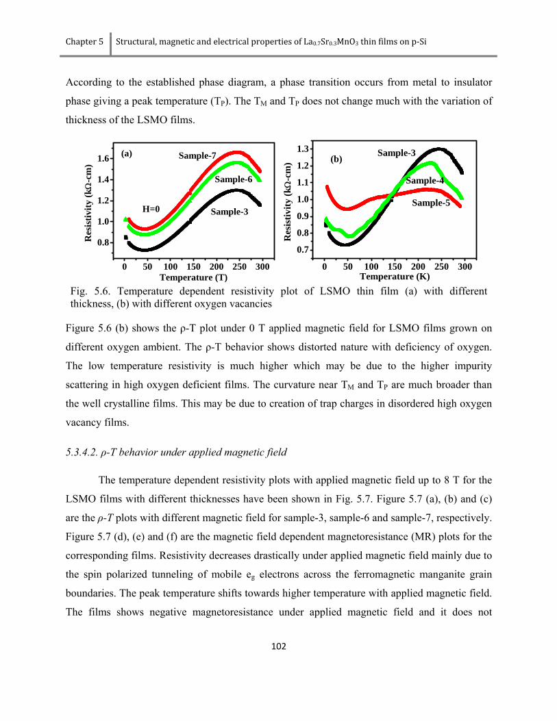
Chapter 5 Structural, magnetic and electrical properties of La0.7Sr0.3MnO3 thin films on p‐Si
102
According to the established phase diagram, a phase transition occurs from metal to insulator
phase giving a peak temperature (TP). The TM and TP does not change much with the variation of
thickness of the LSMO films.
Figure 5.6 (b) shows the ρ-T plot under 0 T applied magnetic field for LSMO films grown on
different oxygen ambient. The ρ-T behavior shows distorted nature with deficiency of oxygen.
The low temperature resistivity is much higher which may be due to the higher impurity
scattering in high oxygen deficient films. The curvature near TM and TP are much broader than
the well crystalline films. This may be due to creation of trap charges in disordered high oxygen
vacancy films.
5.3.4.2. ρ-T behavior under applied magnetic field
The temperature dependent resistivity plots with applied magnetic field up to 8 T for the
LSMO films with different thicknesses have been shown in Fig. 5.7. Figure 5.7 (a), (b) and (c)
are the ρ-T plots with different magnetic field for sample-3, sample-6 and sample-7, respectively.
Figure 5.7 (d), (e) and (f) are the magnetic field dependent magnetoresistance (MR) plots for the
corresponding films. Resistivity decreases drastically under applied magnetic field mainly due to
the spin polarized tunneling of mobile eg electrons across the ferromagnetic manganite grain
boundaries. The peak temperature shifts towards higher temperature with applied magnetic field.
The films shows negative magnetoresistance under applied magnetic field and it does not
Fig. 5.6. Temperature dependent resistivity plot of LSMO thin film (a) with different thickness, (b) with different oxygen vacancies
0 50 100 150 200 250 300
0.8
1.0
1.2
1.4
1.6 Sample-7
Sample-6
Res
istiv
ity (k
Ω-c
m)
Temperature (T)
Sample-3H=0
(a)
0 50 100 150 200 250 300
0.7
0.8
0.9
1.0
1.1
1.2
1.3
Sample-5
Res
istiv
ity (k
Ω-c
m)
Temperature (K)
Sample-3
Sample-4
(b)

Structural, magnetic and electrical properties of La0.7Sr0.3MnO3 thin films on p‐Si Chapter 5
103
changes much with the film thickness. Hwang et al. [19] has described a model for spin polarized
tunneling MR across the ferromagnetic manganite grain boundaries as,
3
0
)( KHJHdkkfAMRH
−−−= ∫ (5.2)
In zero field the domain boundaries are pinned at the grain boundary pinning centre with pinning
strength k. The grain boundaries have a distribution of pinning strength f(k) defined as the
minimum field needed to overcome a particular pinning barrier [20],
)exp()exp()( 222 DkCkBkAkf −+−= (5.3)
A, B, C, D, J and K are the parameters. The best fit values of the parameters have been listed in
Table 5.4 for all the LSMO films. The spin polarized tunneling MR ( ∫−=H
spt dkkfMR0
)( ) and
intrinsic MR (MRint) contributions have be evaluated using all the fit parameters keeping H = 8 T
for each LSMO films as listed in Table 5.4.
Fig. 5.7. Temperature dependent resistivity under applied magnetic field for (a) sample-3, (b) sample-6 and (c) sample-7; (d), (e) and (f) are corresponding % MR plot of the films with applied magnetic field.
0 50 100 150 200 250 3000.4
0.6
0.8
1.0
1.2
1.4
1.6
Res
istiv
ity (k
Ω-c
m)
Temperature (K)
Sample-6
0 50 100 150 200 250 3000.40.50.60.70.80.91.01.11.21.3
8 T7 T6 T5 T4 T3 T2 T1 T
Res
ista
nce
(kΩ
−cm
)
T(K)
0 T
Sample-3
0 2 4 6 8-50
-40
-30
-20
-10
0
2.8 K 5 K 10 K 50 K 100 K 150 K 200 K 250 K 300 K
% M
R
Magnetic Field (T)
0 50 100 150 200 250 3000.4
0.6
0.8
1.0
1.2
1.4
1.6
Res
istiv
ity (k
Ω-c
m)
Temperature (K)
Sample-7
0 2 4 6 8-50
-40
-30
-20
-10
0
2.8 K 5 K 10 K 50 K 100 K 150 K 200 K 250 K 300 K
% M
R
Magnetic field (T)0 2 4 6 8
-50
-40
-30
-20
-10
0 2.8 K 5 K 10 K 50 K 100 K 150 K 200 K 250 K 300 K
% M
R
Magnetic field (T)
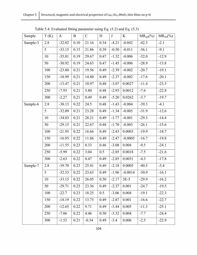
Chapter 5 Structural, magnetic and electrical properties of La0.7Sr0.3MnO3 thin films on p‐Si
104
Table 5.4. Evaluated fitting parameter using Eq. (5.2) and Eq. (5.3)
Sample T (K) A B C D J K MRspt(%) MRint(%)
Sample-3 2.8 -32.02 0.10 21.16 0.34 -4.21 -0.042 -42.3 -2.1
5 -33.15 0.15 21.86 0.39 -0.50 -0.011 -36.1 -9.1
10 -35.81 0.19 29.67 0.47 -1.32 -0.006 -32.0 -12.9
50 -30.92 0.19 24.63 0.47 -1.45 -0.006 -28.9 -13.8
100 -23.80 0.21 19.56 0.49 -2.39 -0.002 -20.7 -19.1
150 -18.99 0.21 14.80 0.49 -2.37 -0.002 -17.6 -20.1
200 -13.47 0.21 10.97 0.48 -3.07 0.0027 -11.4 -23.3
250 -7.93 0.21 5.80 0.48 -2.93 0.0012 -7.6 -22.8
300 -2.27 0.21 0.49 0.49 -5.20 0.0262 -3.7 -19.7
Sample-6 2.8 -38.13 0.22 24.5 0.48 -1.43 -0.004 -39.3 -4.1
5 -32.09 0.21 23.28 0.49 -1.34 -0.005 -31.9 -12.6
10 -34.03 0.21 28.21 0.49 -1.77 -0.001 -29.3 -14.4
50 -29.15 0.21 22.67 0.48 -1.70 -0.003 -26.1 -15.6
100 -21.95 0.22 16.66 0.49 -2.43 0.0003 -19.9 -18.7
150 -16.95 0.22 11.86 0.49 -2.47 -0.0005 -16.7 -19.8
200 -11.55 0.23 8.33 0.46 -3.08 0.004 -9.5 -24.1
250 -5.99 0.22 3.04 0.5 -2.85 0.0018 -7.5 -21.6
300 -2.63 0.22 0.47 0.49 -2.85 0.0031 -4.3 -17.8
Sample-7 2.8 -39.70 0.23 25.41 0.49 -2.18 0.0005 -40.5 -5.4
5 -32.53 0.22 23.63 0.49 -1.96 -0.0014 -30.9 -16.1
10 -33.15 0.22 26.05 0.50 -2.17 3E-5 -29.9 -16.2
50 -29.71 0.23 23.36 0.49 -2.37 0.001 -24.7 -19.5
100 -22.7 0.23 18.25 0.5 -3.06 0.004 -19.1 -22.3
150 -18.19 0.22 13.75 0.49 -2.87 0.001 -16.6 -22.7
200 -12.65 0.22 9.71 0.49 -3.44 0.005 -11.3 -25.1
250 -7.06 0.22 4.46 0.50 -3.32 0.004 -7.7 -24.4
300 -1.52 0.21 -0.34 0.49 -3.4 0.006 -2.5 -22.9

Structural, magnetic and electrical properties of La0.7Sr0.3MnO3 thin films on p‐Si Chapter 5
105
The % of MRspt drops sharply, where as the % of MRint increases with increasing temperature.
The temperature dependent % of MRspt can be explained using an empirical expression
( )/()( TcbaMRspt ++= [19].
5.3.4.2.1. ρ-T behavior below TM
Focusing on the resistivity plot again, it is necessary to study the appearance of low
temperature minima and peak temperature and their dependence on magnetic field. To explore
the fact we have chosen the ρ-T behavior of the sample-3. The low temperature ρ-T behavior
below resistivity minimum (TM) showing resistivity upturn in all LSMO thin films can have
various source of origin. At low temperatures, low resistive dilute alloys with very small
magnetic impurity generally show Kondo resistivity minima and the ρ(T) relation is given by
[21]
)ln()( 0 TCT −= ρρ (5.4) where ρ0 is the residual resistivity. The Kondo resistivity minima are attributed to the localized
magnetic impurities that are far apart and interact by polarizing electrons. The Kondo minima
disappear with the application of external magnetic field.
Moreover, in the disordered highly resistive systems the mean free path of conduction
electrons become small and they involve in multiple elastic scattering [22]. It causes a higher
resistivity in the system. Any inelastic process or electron-electron interaction or applied
magnetic field can reduce the resistivity. A resistivity minimum occurs at TM because there is
ultimately an increase of resistivity with temperature due to inelastic high temperature electron-
phonon scattering. Below the resistivity minima due to the electron-electron interaction the ρ(T)
relation is given by [23], 2/1
0)( BTT −= ρρ (5.5)
On the other hand, the resistivity due to the temperature dependent other scatterings like
electron-phonon, electron-magnon can be expressed as, nATT =)(ρ (5.6)
Figure 5.8 shows the low temperature minima of sample-3 with different applied
magnetic fields up to 8 T. The resistivity curves lower than TM (T < TM) have been fitted
considering both Kondo effect and electron-electron correlation effect as described in Eq. (5.4)

Chapter 5 Structural, magnetic and electrical properties of La0.7Sr0.3MnO3 thin films on p‐Si
106
and Eq. (5.5). The temperature dependent inelastic term (Eq. 5.6) has been added with these
equations and hence we can write, nATTCT +−= )ln()( 0ρρ (5.7)
nATBTT +−= 2/10)( ρρ (5.8)
All the ρ(T) curves measured at different magnetic fields below TM have been fitted with
both Eq. (5.7) and Eq. (5.8) as shown in Fig. 5.8. Figure 5.8(a) is the low temperature ρ(T)
curves fitted with Eq. (5.8) (red lines) and Fig. 5.8(b) is the same fitted with Eq. (5.7) (green
lines). The best fit χ2 values for both the fits have been examined and it is found that the Eq. (5.8)
fits much better as compared to Eq. (5.7). Comparative % of deviation of fit with Kondo effect
and e-e interaction effect for the ρ(T) curves with 0 T and 8 T applied magnetic field have been
shown in Fig 5.8(c) and (d), respectively. It clearly shows that the e-e interaction model fits
much better thereby explaining best possible electronic transport mechanism at very low
temperature in these LSMO thin films. The evaluated parameters fitting with Eq. (5.8) have been
summarized in Table 5.5. From the Table 5.5 it is clear that the coefficient B (e-e interaction
term) in Eq. (5.8) remains unaltered with the application of magnetic field. However, the
coefficient A changes noticeably with the magnetic field keeping the value of the exponent n ~ 2
( ~ AT2). So the origin of this additional term in Eq.(5.8) possibly arises due to the electron-
magnon scattering process these films.
0 10 20 30 40 500.4
0.5
0.6
0.7
0.8
Res
istiv
ity (k
Ω-c
m)
Temperature (K)
Kondo minima
(b)
10 20 30 40 50
-0.8
-0.4
0.0
0.4
0.8
% o
f D
evia
tion
Temperature (K)
Kondo Effect
e-e interactionH=0
(c)
10 20 30 40 50
-0.2
-0.1
0.0
0.1
0.2
% o
f dev
iatio
n
Temperature (K)
Kondo Effect
e-e interaction
(d)
H=8 T
0 10 20 30 40 500.4
0.5
0.6
0.7
0.8
0.9
0T0T0T0T0T0T0T
Res
istiv
ity (k
Ω−c
m)
Temperature (K)
0T
e-e interation
(a)
Fig. 5.8. Low temperature ρ(T) curves fitted with (a) electron-electron interaction model, (b) Kondo Effect model; (c) and (d) are % of deviation of fit values at 0 and 8 T. The deviation clearly shows the good fit with e-e interaction model.

Structural, magnetic and electrical properties of La0.7Sr0.3MnO3 thin films on p‐Si Chapter 5
107
Table 5.5: Fit parameters evaluated using Eq. (5.8).
Magnetic field
(T)
ρ0 (kΩ-cm) B (kΩ-cmK-1/2) A ((kΩ-cmK-n)
×10-3
n
0 0.912 0.0385 0.742 1.82
1 0.675 0.0314 2.143 1.57
2 0.639 0.0282 1.343 1.66
3 0.613 0.0277 1.612 1.61
4 0.589 0.0272 2.061 1.55
5 0.567 0.0268 2.393 1.51
6 0.547 0.0259 2.396 1.50
7 0.529 0.0266 3.672 1.41
8 0.510 0.0256 3.589 1.41
The depth of minima )6.1(/)]()6.1([ KTK M ρρρ − has been plotted with magnetic field as
shown in Fig. 5.9. The depth of minima initially decreases slightly with the magnetic field till
2 T beyond which it becomes almost field independent.
5.3.4.2.2. ρ-T behavior above TM
The temperature dependent resistivity above TM and below TP (metal-insulator transition
temperature) as shown in Fig. 5.7(a) has been best described with the help of Matthiessen’s law
as described below [24]:
0 2 4 6 80.115
0.120
0.125
0.130
0.135
0.140
Dep
th o
f min
ima
Magnetic field (T)
Fig. 5.9. Magnetic field dependent

Chapter 5 Structural, magnetic and electrical properties of La0.7Sr0.3MnO3 thin films on p‐Si
108
mlT ρρρρ ++= 0)( (5.9)
where, ρ0 is residual resistivity. The two other resistivity terms (ρl and ρm) originate from the
scattering of lattice phonon and spin wave at finite temperatures, respectively. For both lattice
and magnetic scatterings conduction electrons might undergo s-s and s-d transitions. The
scattering due to lattice have been given by [25],
∫ −−−⎟⎟⎠
⎞⎜⎜⎝
⎛=
T
xx
nn
Dl
D
eedxxTA
θ
θρ
0 )1)(1( (5.10)
where, the θD is the Debye temperature; n is a constant generally it is 3 for magnetic metal and
alloys with large d-band density of state.
The resistivity due to exchange interaction between the conduction electrons (s) and the
localized magnetic electrons (3d) is ρm. This interaction is generally called the s-d interaction.
This spin disorder resistivity goes with the 2nd power of temperature ( 2)( DTT =ρ ) where, D
shows the strength of s-d interaction. Eq.(5.9) fits well with the all ρ(T) curves in this
temperature regimes and describes well the electron transport mechanism in these LSMO films.
5.4. Summary
The LSMO thin films with different thicknesses and different oxygen vacancies have
been grown on SiO2/p-Si substrates where the SiO2 layer have been created by oxidation of Si.
All the films show nano rod like growth with high texturing towards (100) direction. The growth
of the film is almost linear with deposition time implying good uniformity of the films.
The magnetization measurement of the film shows good ferromagnetic nature at all
temperatures with saturation field near 0.07 T. The FC and ZFC curves show strong
irreversibility exhibiting prominent maximum at Tmax (~ 130 K). The sharp decrease of low field
ZFC curve at low temperature and the increase of irreversibility with decreasing temperature
generally are attributed to the passage from a ferromagnetic state to a low temperature disordered
surface regime.
Structural, magnetic and electrical properties of La0.7Sr0.3MnO3 thin films on p‐Si Chapter 5
109
The temperature dependent resistivity shows the metal-insulator transition giving a peak
temperature near 250 K. The peak temperature does not change, though the resistivity increases
slightly with decreasing thickness. The distortion in ρ-T curves for oxygen deficient films may be
due to the oxygen vacancy and lattice defects. The low temperature resistivity is much higher
which may be due to the higher impurity scattering in high oxygen deficient films. The curvature
near TM and TP are much broader than the well crystalline film possibly due to the creation of
trap charges in disordered high oxygen vacancy films. All the films show negative MR behavior
for temperatures up to 300 K and there is not much effect of film thickness in that thickness
range. Resistivity decreases sharply with the application of magnetic field in the low magnetic
field region mainly due to the spin polarized tunneling of mobile eg electrons across the
ferromagnetic manganite grain boundaries. The MR contribution due to extrinsic spin polarized
tunneling across the grain boundaries as well intrinsic CMR inside grains has also been separated
out for the films.
The resistivity behavior in the temperature range lower than TM has been well described
through the electron-electron interaction model rather than the Kondo effect. The dependency of
parameter A with applied magnetic field and the depth of minima indicate the electron-magnon
scattering process in the films. The resistivity behavior in the higher temperature regime (> TM)
has been described through the lattice and magnetic scattering using the Matthiessen’s law.
References
[1] P. Dey, T. K. Nath and A. Banerjee, Enhanced grain surface effect on magnetic properties of La0.5Gd0.2Sr0.3MnO3 nanoparticles: A comparison with bulk counterpart, Appl. Phys. Lett. 91, 012504 (2007). [2] P. Dey and T. K. Nath, Tunable room temperature low-field spin polarized tunneling magnetoresistance of La0.7Sr0.3MnO3 nanoparticles, Appl. Phys. Lett. 89, 163102 (2006). [3] P. Dey and T. K. Nath, Effect of grain size modulation on the magneto- and electronic-transport properties of La0.7Ca0.3MnO3 nanoparticles: The role of spin-polarized tunneling at the enhanced grain surface, Phys Rev. B 73, 214425 (2006). [4] J. Fontcuberta, M. Bibes, and B. Martı´nez, V. Trtik, C. Ferrater, F. Sa´nchez, and M. Varela, Tunable epitaxial growth of magnetoresistive La2/3Sr1/3MnO3 thin films, J. Appl. Phys. 85, 4800 (1999). [5] V. Moshnyaga, I. Khoroshun, A. Sidorenko, P. Petrenko, A. Weidinger, M. Zeitler, B. Rauschenbach, R. Tidecks, and K. Samwer, Preparation of rare-earth manganite-oxide thin films by metalorganic aerosol deposition technique, Appl. Phys. Lett. 74, 2842 (1999).
Chapter 5 Structural, magnetic and electrical properties of La0.7Sr0.3MnO3 thin films on p‐Si
110
[6] A. Goyal, M. Rajeswari, R. Shreekala, S. E. Lofland, S. M. Bhagat, T. Boettcher, C. Kwon, R. Ramesh, and T. Venkatesan, Material characteristics of perovskite manganese oxide thin films for bolometric applications, Appl. Phys. Lett. 71, 2535 (1997). [7] A. Urushibara, Y. Moritomo, T. Arima, A. Asamitsu, G. Kido and Y. Tokura, Insulator-metal transition and giant magnetoresistance in La1-xSrxMnO3, Phys. Rev. B 51, 14103 (1995). [8] P. Schiffer, A. P. Ramirez, W. Bao, and S. W. Cheong, Low Temperature Magnetoresistance and the Magnetic Phase Diagram of La1-xCaxMnO3, Phys. Rev. Lett. 75, 3336 (1995). [9] Y. Tokura, Y. Tomioka, H. Kuwahara, A. Asamitsu, Y. Moritomo, and M. Kasai, Origins of colossal magnetoresistance in perovskite-type manganese Oxides, J. Appl. Phys. 79, 5288 (1996). [10] S. Jin, T. H. Tiefel, M. McCormack, R. A. Fastnacht, R. Ramesh and L. H. Chen, Thousand fold Change in Resistivity in Magnetoresistive La-Ca-Mn-O Films, Science 264, 413 (1994). [11] J. D. Boeck, Switching with Hot Spins, Science 281, 357 (1998). [12] G. A. Prinz, Magnetoelectronics, Science 282, 1660 (1998). [13] U. R. Singh, A. K. Gupta, G. Sheet, V. Chandrasekhar, H. W. Jang, and C. B. Eom, Pseudo-gap formation in the metallic state of La0.7Sr0.3MnO3 thin films, Appl. Phys. Lett. 93, 212503 (2008). [14] P. Dey, T. K. Nath, and A. Taraphder, Effect of substrate-induced strain on transport and magnetic properties of epitaxial La0.66Sr0.33MnO3 thin films, Appl. Phys. Lett. 91, 012511 (2007). [15] S. H. Kim, H. J. Sohn, Y. C. Joo, Y. W. Kim, T. H. Yim, H. Y. Lee, T. Kang, Effect of saccharin addition on the microstructure of electrodeposited Fe–36 wt.% Ni alloy, Surf. Coat. Tech. 199, 43 (2005). [16] P. Dey and T. K. Nath, Tunable room temperature low-field spin polarized tunneling magnetoresistance of La0.7Sr0.3MnO3 nanoparticles, Appl. Phys. Lett. 89, 163102 (2006). [17] D. Fiorani, Surface effect in magnetic nanoparticles, Springer (2005). [18] A. P. Ramirez, Colossal magnetoresistance, J. Phys. Conds. Mat. 9, 8171 (1997). [19] H. Y. Hwang, S. W. Cheong, N. P. Ong, and B. Batlogg, Spin-Polarized Intergrain Tunneling in La2/3Sr1/3MnO3, Phys. Rev. Lett. 77, 2041 (1996). [20] P. Raychaudhuri, T. K. Nath, A. K. Nigam and R. Pinto, A phenomenological model for magnetoresistance in granular polycrystalline colossal magnetoresistive materials: The role of spin polarized tunneling at the grain boundaries, J. Appl. Phys. 84, 2048 (1998). [21] J. Kondo, Resistance Minimum in Dilute Magnetic Alloys, Prog. Theo. Phys. 32, 37 (1964). [22] G. Bergmann, Weak localization in thin films: a time-of-flight experiment with conduction electrons, Phys. Rep. 107, 1 (1984). [23] P. A. Lee and T. V. Ramakrishnan, Disordered electronic systems, Rev. Mod. Phy. 57, 287 (1985). [24] P. Khatua, T. K. Nath, Mitali Banerjee, and A. K. Majumdar, Quantum interference effects and magnetic scattering in the electrical resistivity of Ni nanocrystallites in TiN matrix, Appl. Phys. Lett. 92, 193106 (2008). [25] A. H. Wilson, The Electrical Conductivity of the Transition Metal, Prog. R. Soc. London A 167, 580 (1938).
Chapter 6
Junction magnetoresistance study in
La0.7Sr0.3MnO3/SiO2/p-Si heterostructures
This chapter is based on
International journals 1. Electrical and magnetoelectronic properties of La0.7Sr0.3MnO3/SiO2/p‐Si heterostructure for spintronics application,
S. Chattopadhyay, P. Dey and T. K. Nath, Current Applied Physics (In press) doi:10.1016/j.cap.2011.02.009 2. On investigation of origin of junction magnetoresistance in La0.7Sr0.3MnO3/SiO2/p‐Si heterostructures, S.
Chattopadhyay and T. K. Nath, Journal of Physics D: Applied Physics (Communicated)
Conferences/Symposia 1. Investigation on La0.7Ca0.3MnO3/SiO2/n‐Si and La0.7Sr0.3MnO3/SiO2/p‐Si MOS like heterostructures for Spintronics by
S. Chattopadhyay, S. K. Giri and T. K. Nath, International Conference on Fundamental & Applications of Nanoscience and Technology (ICFANT) (2010).
2. Electrical properties of La0.7Sr0.3MnO3/SiO2/Si MOS structure by S. Chattopadhyay, P. Dey, T. K. Nath 53rd DAE Solid State Physics Symposium (2008)
3. I‐V characteristics of La0.7Sr0.3MnO3/SiO2/Si MOS structure by S. Chattopadhyay, P. Dey, T. K. Nath National Seminar on Advanced Nanomaterials and its Applications (2008)

Junction magnetoresistance in La0.7Sr0.3MnO3/SiO2/p‐Si heterostructures
Chapter 6
111
6.1. Introduction
After Datta-Das transistor [1], there is an enormous development of spintronic
devices in the area of microelectronics. Spintronics is a multidisciplinary field whose
central theme is the active manipulation of spin degrees of freedom in solid-state systems.
Generation of spin polarization usually means creating a non-equilibrium spin population
which can be achieved in several ways. For device applications electrical spin injection is
more desirable. In electrical spin injection a magnetic electrode is connected to the
sample. When the current drives spin-polarized electrons from the electrode to the
sample, non-equilibrium spin accumulates there. The rate of spin accumulation depends
on spin relaxation, the process of bringing the accumulated spin population back to
equilibrium. These properties of spin lead to open up new area of spintronic devices such
as magnetic sensors, magnetic devices, photosensitive devices etc [2-4]. Typical time
scales for spin relaxation in electronic systems are measured in nanoseconds, while the
range is from picoseconds to microseconds for electrons, which can be very useful for
high speed magneto-optic devices [5]. Spin detection, also a part of a generic spintronic
scheme, typically relies on sensing the changes in the signals caused by the presence of
non-equilibrium spin in the system. The common goal in many spintronic devices is to
maximize the spin detection sensitivity to the point that it detects not the spin itself, but
changes in the spin states.
Manganite-based heterojunctions such as half-metalic colossal magnetorsistance,
materials with extremely high degree of spin polarization [)()()()(
FF
FF
ENENENEN
S↓↑
↓↑
+
−= ] have
recently attracted lot of attention for their various fields of applications. Recently, a lot of
research studies have been focused on perovskite based oxide semiconductors or
semimetals heterojunctions with different semiconductors [6-8]. Generally the current-
voltage characteristic is guided by tunneling of conduction electrons between the
junctions though the presence of edge leakage makes the transport mechanism
complicated. As a result there is difficulty in the extraction of actual barrier height.
Lanthanum Strontium Manganese Oxide with composition La0.7Sr0.3MnO3 (LSMO), a
colossal magneto-resistive (CMR) ferromagnetic metal at room temperature belongs to

Chapter 6 Junction magnetoresistance study in La0.7Sr0.3MnO3/SiO2/p‐Si heterostructures
112
one of the perovskite type i.e., half-metallic highly spin-polarized ferromagnetic oxides,
hole doped manganites. The resistivity of the LSMO films can be tuned easily during
deposition and is highly stable under further thermal treatment. Moreover, the resistivity
of the materials can also be tuned by applying external magnetic field [9]. So using
LSMO as an electrode in Si/ SiO2/ LSMO heterostructure the I-V and C-V characteristics
can be modulated by applying magnetic field externally and it may open up possibilities
in various technological applications, e.g., magnetic sensors, magnetic memories or other
spin electronic applications. However, the origin of appearing positive junction MR of
these perovskite based heterojunctions is still not understood clearly. Some reports have
concluded that the increase of barrier height due to Zeeman splitting of bands causes the
positive MR at the junction. But, the exact reason is still far from well established.
In this chapter, the junction current density-voltage (J-V) characteristics of
La0.7Sr0.3MnO3 (LSMO)/SiO2/Si junction with and without external magnetic field have
been studied explicitly. The applied external magnetic fields up to 1 T and 8 T have been
exerted on all the heterojunctions using a high precision electromagnet. The constant
parameters of J-V characteristics at room temperature and all other temperature have
been estimated by non-linear least square (χ2- minimization) curve fitting method. The
estimated parameters conclusively show that the series resistance of the junction plays
dominant role to make junction MR positive rather than the effective barrier height. The
effect of leakage currents on junction MR for such heterostructures has also been
established.
6.2. Experimental procedure
The details of sample preparations have been discussed in details in chapter 5
section 5.2. The three best films which show higher value of negative magnetoresistance,
(Film magnetoresistance) have been chosen for heterojunction study. The heterojunctions
and its growth structures and conditions have been summarized in Table 6.1. The
variation of the oxidation time at oxidation temperature 800 °C under oxygen atmosphere
of cleaned high conducting p-Si substrate forms different thermal oxide layer over p-Si
with different thicknesses. The insulating layer between p-Si and La0.7Sr0.3MnO3 (LSMO)
controls the current transport through the heterojunctions.

Junction magnetoresistance in La0.7Sr0.3MnO3/SiO2/p‐Si heterostructures
Chapter 6
113
Table 6.1. The heterojunction structures and its growth conditions
Heterojunction name
Structure of heterojunction
Growth conditions for heterojunction
Film properties
Sample-1 p-Si/SiO2 (native oxide)/
La0.7Sr0.3MnO3 Substrate p-Si; No oxidation ((thickness of SiO2 ~9 Å) La0.7Sr0.3MnO3 have been grown at 800 °C substrate temperature under 0.5 mbar O2 atmosphere
La0.7Sr0.3MnO3
shows rod like structure with -ve magneto-resistance of film
Sample-2 p-Si/SiO2(thermal oxide)/ La0.7Sr0.3MnO3
Substrate p-Si; Oxidation has been carried out for 30 min at 800 °C under oxygen pressure 0.5 mbar (thickness of SiO2 ~40 Å). Then the La0.7Sr0.3MnO3 film have been grown at 800°C substrate temperature under 0.5 mbar O2 atmosphere
La0.7Sr0.3MnO3
shows rod like structure with –ve magneto-resistance film
Sample-3 p-Si/SiO2(thermal oxide)/ La0.7Sr0.3MnO3
Substrate p-Si; Oxidation has been carried out for 45 min at 800 °C under oxygen pressure 0.5 mbar (thickness of SiO2 ~45 Å). Then the La0.7Sr0.3MnO3 film
have been grown at 800 °C substrate temperature under 0.5 mbar O2 atmosphere
La0.7Sr0.3MnO3
shows rod like structure with –ve magneto-resistance in the form of thin film.
Electrical contacts were made with high purity Ag on LSMO film and pure Al contact
with p-Si as ohmic contacts. The temperature and magnetic field dependence I-V
characteristics were measured using a source meter (Keithley 2612), current source
(Keithley 6221), temperature controller (Lakeshore, model-331), high precision
electromagnet (Polytronic, Model HEM 100) and a variable temperature cryostat (Janis,
USA). A cryogen free 8 T superconducting magnet with VTI system down to temperature

Chapter 6 Junction magnetoresistance study in La0.7Sr0.3MnO3/SiO2/p‐Si heterostructures
114
2 K (Cryogenics, U.K.) has been employed for high field and low temperature transport
measurements.
6.3 Results and discussion
6.3.1 Structural properties
The x-ray diffraction pattern of LSMO film (sample-3) deposited on (100) p-Si
substrate using Cu-Kα radiation has been shown in Fig. 6.1. The multipeaks from
different crystallographic planes of LSMO sample reveal the non-epitaxial nature of the
LSMO film on SiO2/Si layer as discussed in chaper-5. In Fig. 6.1(b) and 6.1(c) the
FESEM micrograph of the LSMO film (sample-3) and the cross sectional FESEM image
of the heterojunction have been shown. The FESEM micrograph clearly shows the
uniformly grown smooth LSMO film with good coverage on Si/SiO2 layer. The cross-
sectional FESEM picture reveals the nano-rod like growth of the film with film thickness
~ 600 nm.
6.3.2. Electrical properties of LSMO/SiO2/p-Si hereostructure without applied magnetic
field
6.3.2.1. Current-Voltage study using diode characteristics
Figure 6.2(a) shows the non-linear current density-voltage (J-V) characteristics of
a typical LSMO/SiO2/Si structured heterojunction measured at room temperature. It can
(a)
(c)
(b)
(c)
(a)
Fig. 6.1. (a) XRD pattern of LSMO/SiO2/p-Si hereostructure. Inset shows the XRD pattern of LSMO film. (b) and (c) FESEM micrograph of LSMO film and crosssectional view of the heterostructure.

Junction magnetoresistance in La0.7Sr0.3MnO3/SiO2/p‐Si heterostructures
Chapter 6
115
be seen that the junctions exhibit diode-like behavior. The J-V characteristics of the films
are found to depend strongly on the interfacial oxides layer. The ideality factor η is much
greater than 2 at room temperature. At low forward voltage the current increased
exponentially which has been usually observed in diodes and attributed to recombination,
tunneling mechanism. At moderate junction voltage the J-V deviated from ideal
thermionic emission and behaves as J~V2 relation which is attributed to space charge
limited current (SCLC) conduction. Applied voltage lower than the turn on voltage shows
ohmic behavior. All the regions have been distinctly shown in log J - log V plot of Fig.
6.2(b). The junction J-V characteristics are described as [10],
⎟⎟⎠
⎞⎜⎜⎝
⎛ −−=
kTIRVVe
JJ s
η)(
exp 00 (6.1)
where, J0 is the reverse saturation current density. V0, η, and Rs are turn on voltage,
ideality factor and junction series resistance respectively. The fitted values of the
parameters for different samples have been plotted in Fig. 6.2(c) and Fig. 6.2(d),
respectively. The decrease of ideality factor and reverse saturation current density [in Fig.
6.2(c)] and increase of turn on voltage and series resistance [in Fig. 6.2(d)] with
increasing the oxidation time illustrates that the leakage current and defect induced
tunneling through the junction decreases effectively with the enhancement of oxidation
time (thickness of the intermediate SiO2 oxide layer). As the native oxide layer contains
inherently high density of oxide defect states in it, the leakage current becomes large at
room temperature that enhances the junction forward current and causes lower series
resistance through the junction. When the oxide layer is grown over the Si substrate
thermally in O2 atmosphere the oxide defects decreases as well as the thickness of the
oxide layer increases. So, both the leakage current and tunneling probability through the
oxide interface decreases. It causes enhancement of series resistance from sample-1 to
sample-3.

Chapter 6 Junction magnetoresistance study in La0.7Sr0.3MnO3/SiO2/p‐Si heterostructures
116
The J-V characteristics for sample-3 at several temperatures down to 77 K have
been shown in Fig. 6.3(a). It shows that the current decreases with decreasing
temperature. The best fit parameters (η, J0, Rs and V0) for all three samples have been
evaluated for all six temperatures down to 77 K using Eq. (6.1) employing a χ2
minimization technique. All these temperature dependent fit parameters are shown in Fig.
6.3(b) and 6.3(c). The strong dependency of current density and all four parameters with
temperature indicates that not only the thermionic emission is occurring at the junction
but other types of transport mechanisms are also present for all the heterojunctions. The
strong dependency of ideality factor with temperature implies that the tunneling
mechanism is one of the dominating current transport mechanisms through the junction.
-6 -4 -2 0 2 4 6-0.15
-0.10
-0.05
0.00
0.05
0.10
0.15
0.20
sample-1 sample-2 sample-3
C
urre
nt d
ensi
ty (m
A/c
m2 )
Voltage (V)
300 K
1 10
1
10
100
Cur
rent
den
sity
(μA
/cm
2 )
Voltage (V)
Ohmic region
Tunneling region
SCLC region
Sample-2
300 K
0 10 20 30 40 508
12
16
20
24
28
32
η J0
Oxidation time (min)
η
300 K
1.0
1.5
2.0
2.5
3.0
3.5
4.0
J0 (μA/cm
2)
0 10 20 30 40 500
10
20
30
40
50
60
70
80
RS
V0
Oxidation time (min)
Seri
es R
esis
tanc
eRS(
kΩ−c
m2 )
300 K
0.50
0.52
0.54
0.56
0.58
0.60
0.62
Turn on voltage V
0 (V)
(a) (b)
(c) (d)
Fig.6.2: (a) J-V characteristics of LSMO/SiO2/p-Si heterojunction for three different samples at room temperature. (b) log J-log V plot of sample-2 to understand the current transport process at room temperature. (c) and (d) are evaluated fit parameters at room temperature. The ideality factors, reverse saturation current density plot for three different samples have been shown in (c), and series resistance and turn-on voltage have been shown in (d).

Junction magnetoresistance in La0.7Sr0.3MnO3/SiO2/p‐Si heterostructures
Chapter 6
117
The ln(J0/T2) vs. 1000/T plot shown in Fig. 6.3(d) provides the information about the
effective barrier height and Richardson constant for all the three samples.
Table 6.2. Effective barrier height and Richardson constants for different samples
Sample name Effective barrier height (eV) Richardson constant (AK-2cm-2)
Sample-1 0.021 7.05 × 10⁻⁹
Sample-2 0.027 1.7 × 10⁻⁸
Sample-3 0.030 7.62 ×10⁻⁹
The evaluated values have been summarized in the Table 6.2. The slight difference in the
value of Richardson constants may be due to different effective masses in the films. The
0 2 4 6 8 100
20
40
60 77 K 120 K 150 K 200 K 250 K 300 K
Cur
rent
den
sity
(μA
/cm
2 )
Voltage (V)
Sample-3
(a)
50 100 150 200 250 3000
100
200
300
400
500
sam
ple-
3 sample-2
sample-1
sample-3
sample-2
sample-1
Temperature (K)
Seri
es r
esis
tanc
e (kΩ
-cm
2 )
0
2
4
6 RS V0
Turn on voltage (V
0 ) (V)(c)
2 4 6 8 10-19.6
-19.2
-18.8
-18.4
-18.0
-17.6
-17.2
-16.8
-16.4
Sample-2
Sample-1
ln(J
0/T
2 )
1000/T (K-1)
Sample-3
(d)
100 150 200 250 300
10
20
30
40
50
60
70
80
sample-3
sample-2
sample-1
sample-3
sample-2
sample-1
Temperature (K)η
0
1
2
3
4 η J0 J
0 (μA/cm
2)
(b)
Fig. 6.3. (a) Temperature dependent J-V characteristics of sample-3 without applied magnetic field. (b) and (c) are the plot of evaluated parameters with temperature. The ideality factor and reverse saturation current density plot with temperature for three different samples have been shown in (b), and series resistance and turn-on voltage with temperature have been shown in (c). (d) ln(I0/T2) vs. 1000/T plot to determine the effective barrier height.

Chapter 6 Junction magnetoresistance study in La0.7Sr0.3MnO3/SiO2/p‐Si heterostructures
118
barrier height is much lower than expected because of high leakage current through the
junction.
6.3.2.2. Tunneling Characteristics
The I-V properties reveal that tunneling is occurring at all temperatures along
with other mechanisms through our heterojunction as discussed earlier. Now it is
necessary to find out the possible tunneling mechanism through the heterojunctions. The
observed field stimulated emission and capture have been discussed in terms of Fowler-
Nordheim tunneling [11], Poole-Frenkel effect [12–14], phonon assisted tunneling [15],
and a combination of both phenomena [16-20]. Fowler-Nordheim tunneling is the process
whereby electrons tunnel through a barrier in the presence of a high electric field. This
quantum mechanical tunneling process is an important mechanism for thin barriers
similar to those in metal-semiconduictor junctions on highly-doped semiconductors.
Fowler-Nordheim (F-N) tunneling current into the SiO2 conduction-band through a
triangular barrier at high field is given by,
)/exp(2 VBAVJ FN −= (6.2)
where, Bh
qAφπ8
3= and
qhm
B BFN
3)2(8 2/32/1 φπ
= . Here q is the electronic charge, Bφ and mFN
are the effective tunneling barrier height and effective mass of electron for F-N tunneling.
V is the applied electric field across the thin oxide layer. The high field Fowler-Nordheim
(F-N) plot [ln(JFN/V2) vs 1/V] of the heterojunction with native (sample-1) and thermal
oxide intermediate layer (sample-3) at different temperatures have been shown in Fig.
6.4(a) and 6.4(b). The high field Fowler-Nordheim tunneling should be temperature
independent. But our observed [ln(JFN/V2) vs 1/V] is strongly temperature dependent and
hence we can conclude that the field dependent tunneling is mainly temperature
dependent Frenkel-Poole type emission.
The well-known Frenkel-Poole effect describes the increase of the thermal
emission rate of carriers in an external electric field due to the lowering of the barrier
associated with their Coulomb potential. It is a classical mechanism in which the electron
is thermally emitted over the top of a potential barrier which has been lowered by the
presence of an electric field.
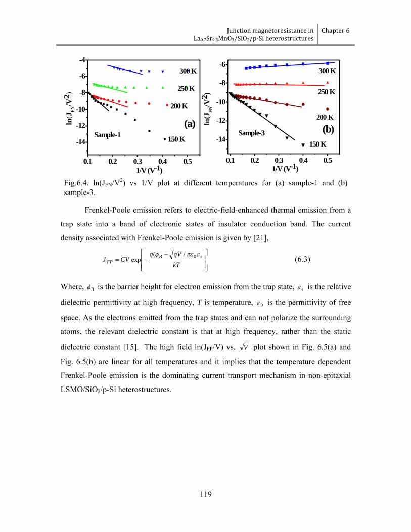
Junction magnetoresistance in La0.7Sr0.3MnO3/SiO2/p‐Si heterostructures
Chapter 6
119
Frenkel-Poole emission refers to electric-field-enhanced thermal emission from a
trap state into a band of electronic states of insulator conduction band. The current
density associated with Frenkel-Poole emission is given by [21],
⎥⎥⎦
⎤
⎢⎢⎣
⎡ −−=
kTqVq
CVJ sBFP
επεφ 0/(exp (6.3)
Where, Bφ is the barrier height for electron emission from the trap state, sε is the relative
dielectric permittivity at high frequency, T is temperature, 0ε is the permittivity of free
space. As the electrons emitted from the trap states and can not polarize the surrounding
atoms, the relevant dielectric constant is that at high frequency, rather than the static
dielectric constant [15]. The high field ln(JFP/V) vs. V plot shown in Fig. 6.5(a) and
Fig. 6.5(b) are linear for all temperatures and it implies that the temperature dependent
Frenkel-Poole emission is the dominating current transport mechanism in non-epitaxial
LSMO/SiO2/p-Si heterostructures.
0.1 0.2 0.3 0.4 0.5
-14
-12
-10
-8
-6
-4300 K
250 K
200 K
ln(J
FN/V
2 )
1/V (V-1)
Sample-1 150 K
(a)
0.1 0.2 0.3 0.4 0.5
-14
-12
-10
-8
-6
300 K
250 K
200 K
ln(J
FN/V
2 )
1/V (V-1)
150 KSample-3 (b)
Fig.6.4. ln(JFN/V2) vs 1/V plot at different temperatures for (a) sample-1 and (b) sample-3.

Chapter 6 Junction magnetoresistance study in La0.7Sr0.3MnO3/SiO2/p‐Si heterostructures
120
These plots show linear nature in higher field range confirms the presence of temperature
dependent Frenkel-Poole emission through the heterostructures.
6.3.3. Electrical properties of LSMO/SiO2/p-Si hereostructure with applied magnetic field
The J-V behaviors of sample-3 under very high magnetic field up to 8 T have
been shown in Fig. 6.6(a) and Fig. 6.6(b) at 300 K and 120 K, respectively.
Fig. 6.5. ln(JFP/V) vs. plot for V1/2 at different temperatures for (a) sample-1 and (b) sample-3
0.5 1.0 1.5 2.0 2.5 3.0
-14
-12
-10
-8
-6
-4
300 K
250 K
200 K
√V (V1/2)
ln(J
FP/V
)
150 K
(b)
Sample-3
0.5 1.0 1.5 2.0 2.5 3.0 3.5
-14
-12
-10
-8
-6
-4
300 K
250 K
200 K
ln(J
FP/V
)
√V (V1/2)
150 KSample-1
(a)
Fig. 6.6. The J-V characteristics at 300 K and 120 K in (a) and (b), respectively at different applied magnetic field; the %JMR at 300 K and 120 K in (c) and (d), respectively.
0 1 2 3 4 5 6
0.000.010.020.030.040.050.060.07
0 T 1 T 2 T 4 T 6 T 8 T
Cur
rent
den
sity
(mA
/cm
2 )
Voltage (V)
Sample-3T = 300 K
(a)
0 2 4 6 8 10
0.000
0.002
0.004
0.006
0.008
0.010
Cur
rent
den
sity
(mA
/cm
2 )
Voltage (V)
0 T 1 T 2 T 4 T 6 T 8 T
Sample-3T =120 K
(b)
-8 -6 -4 -2 0 2 4 6 8
0
10
20
30
40
50
60
%JM
R
Magnetic field (T)
Sample-3120 K
(d)
-8 -6 -4 -2 0 2 4 6 8
0
4
8
12
16
20
% J
MR
Magnetic field (T)
Sample-3300 K
(c)

Junction magnetoresistance in La0.7Sr0.3MnO3/SiO2/p‐Si heterostructures
Chapter 6
121
Corresponding junction magnetoresistance have also been shown in Figs. 6.6(c)
and (d), respectively. The change is almost linear up to 1 T magnetic field. After applying
higher magnetic field beyond 1 T, the junction magnetoresistance starts saturating and
applying very high magnetic field (> 4 T), junction magnetoresistance starts to decrease
slightly.
6.3.3.1. Current-Voltage properties under magnetic field using diode characteristics
Figure 6.7 (a) shows the room temperature J-V nature with and without external
magnetic field of 1 T for all three samples.
The J-V curve shows reasonably good sensitivity under magnetic field at room
temperature as shown in Fig. 6.7(a). The four parameters in Eq. (6.1) are modified under
0 10 20 30 40 5012141618202224262830
ηm J0m
Oxidation time (min)
η mT=300 K
0.014
0.016
0.018
0.020
(b)
J0m (m
A/cm
2)
0 10 20 30 40 500
20
40
60
80
100
RSm
V0m
Oxidation time (min)
RSm
(kΩ
-cm
2 )
1.0
1.1
1.2
1.3
1.4
1.5
(c)
V0m (V
)
T =300 K
0 1 2 3 4 5 60.00
0.06
0.12
0.18 sample-1 at 0T sample-1 at 1T sample-2 at 0T sample-2 at 1T sample-3 at 0T sample-3 at 1T
curr
ent d
ensi
ty (m
A/c
m2 )
Voltage (V)
(a)
Fig. 6.7(a) J-V characteristics of LSMO/SiO2/p-Si heterojunction for three different samples at room temperature with and without applied 1 T magnetic field. (b) and (c) are evaluated parameters at room temperature. The ideality factor and reverse saturation current density plot for three different samples under 1 T magnetic field have been shown in (b), and series resistance and turn-on voltage have been shown in (c) at room temperature. (d) The measured %junction MR plot with applied magnetic field for all three samples at room temperature.
-0.8 -0.4 0.0 0.4 0.802468
10121416
(d)
Sample-1 Sample-2 Sample-3
% J
MR
Applied magnetic field (T)
T=300 K

Chapter 6 Junction magnetoresistance study in La0.7Sr0.3MnO3/SiO2/p‐Si heterostructures
122
magnetic field (J0, η, Rs and V0 are now replaced by J0m, ηm, Rsm and V0m, respectively)
and the current density is found to decrease with magnetic field at higher bias potential.
The reverse saturation current density (J0m) and ideality factor (ηm) evaluated from fitting
to room temperature J-V curve under magnetic field for different oxide thickness have
been plotted in Fig. 6.7(b) and series resistance (Rsm) and turn-on voltage (V0m) have
been shown in Fig. 6.7(c). The current has been measured by keeping fixed forward
junction voltage at 4.8 V for varying magnetic field up to 1 T at room temperature. It
shows the change in junction MR is about 7, 9 and 16% at 4.8 V for sample-1, sample-2
and sample-3, respectively. The definition used here for the junction
%100)0()0()1(×⎟⎟⎠
⎞⎜⎜⎝
⎛⎟⎟⎠
⎞⎜⎜⎝
⎛−=
=== THJ
applied
THJ
applied
THJ
applied
IV
IV
IV
MR , where IJ(H=1T) is the current at 1 T applied
magnetic field. The plots of % of junction MR with applied magnetic field at a bias
voltage of 4.8 V for all three samples have been shown in Fig. 6.7(d).
The temperature dependent J-V properties without and with 1 T magnetic field of
sample-3 have been shown in Fig. 6.8(a) for three different temperatures. It shows the
positive junction MR properties for all the temperatures and the magnitude of junction
MR is also temperature dependent. The fit parameters under magnetic field for different
samples have been plotted in Fig. 6.8(b) and Fig. 6.8(c) respectively. The dependency of
all four parameters with temperature show the same trend as the parameters evaluated
from J-V without magnetic field shows. The ln(J0m/T2) vs. 1000/T plot shown in Fig.
6.8(d) provides the information about the effective barrier height and Richardson constant
for all the three heterojunctions under magnetic field. The estimated parameters have also
been listed in the Table 6.3. The evaluated effective barrier heights are not much
increased under magnetic field. But the other parameters, mainly the series resistances are
increased significantly under magnetic field and it cause the positive MR at the
heterojunctions at all operating temperatures.

Junction magnetoresistance in La0.7Sr0.3MnO3/SiO2/p‐Si heterostructures
Chapter 6
123
Table 6.3. Effective barrier height and Richardson constants for three different samples under 1 T magnetic field
Sample name Effective barrier height (eV) Richardson constant AK-2cm-2
Sample-1 0.020 2.73 × 10⁻⁸
Sample-2 0.029 4.22 × 10⁻⁸
Sample-3 0.046 9.21 × 10⁻⁸
The comparative study of barrier height and series resistance with and without magnetic
field has been listed in Table 6.4.
0 2 4 6 8 100.000.010.02
0.030.040.05
0.060.07
(a)
120 K at 0T 120 K at 1T 250 K at 0T 250 K at 1T 300 K at 0T 300 K at 1T
curr
ent d
enst
y (m
A/c
m2 )
Voltage (V)
Sample-3
120 160 200 240 280 320
0
100
200
300
400
500
600
(c)
Sample-3
Sample-2
Sample-1
Sample-3Sample-2
RSm
V0m
Temperature (K)
Rsm
(KΩ−c
m2 )
Sample-1
2
4
6
V0m
(V)
3 4 5 6 7 8 9-19.0-18.5-18.0-17.5-17.0-16.5-16.0-15.5-15.0
(d)ln(J
0m/T
2 )
1000/T (K-1)
sample-3
sample-2
sample-1
120 160 200 240 280 320
20
40
60
80
100
Sam
ple-1
Sample
-3
Sample-3
Sample-2
ηm J0m
Temperature (K)
η m
Sample-1
0.000
0.004
0.008
0.012
0.016
0.020
(b)
J0m (m
A/cm
-2)
Fig. 6.8. (a) Temperature dependent J-V characteristics of sample-3 with and without 1 T applied magnetic field. (b) and (c) are the plot of evaluated parameters with temperature. The ideality factor and reverse saturation current density plot with temperature for three different samples under 1 T magnetic field have been shown in (b), and series resistance and turn-on voltage with temperature under 1 T magnetic field have been shown in (c). (d) ln(I0/T2) vs. 1000/T plot to determine the effective barrier height under magnetic field.

Chapter 6 Junction magnetoresistance study in La0.7Sr0.3MnO3/SiO2/p‐Si heterostructures
124
Table 6.4. Comparative study of effective barrier height and room temperature series resistance with and without applied 1 T magnetic field.
Applied Magnetic
field
Sample name Effective barrier height
(eV)
Series resistance
(kΩ-cm2)
0 T Sample-1 0.021 7.2
Sample-2 0.027 35.42
Sample-3 0.030 74.86
1 T Sample-1 0.020 7.8
Sample-2 0.029 39.34
Sample-3 0.046 89.03
It is clear that the evaluated effective barrier heights are not much increased under
magnetic field. But the other parameters, mainly the series resistances are increased much
under magnetic field and cause the positive MR at the heterojunctions at all operating
temperatures.
6.3.3.2. Tunneling Characteristics under1 T applied magnetic field
As discussed earlier, the dominating tunneling mechanism through the
heretojunctions fits very well with temperature dependent Frenkel-Poole emission. The
ln(JFP/V) vs. V plot for J-V under 1 T applied magnetic field has also been shown in
Fig 6.9(a) and Fig. 6.9(b) for both sample-1 and sample-3, respectively.
In the high biasing field region ln(JFP/V) vs. V graphs have been fitted linearly for both
the sample-1 and sample-3. The intercept at y-axis have been plotted with 1000/T in Fig.
Fig.6.9. (a) ln(JFP/V) vs. plot for V1/2 at different temperatures for (a) sample-1 and (b) sample-3 under 1 T applied magnetic field.
0.5 1.0 1.5 2.0 2.5 3.0 3.5
-14
-12
-10
-8
-6
-4 300 K 250 K
200 K
ln(J
FP/V
)
√V (V1/2)
Sample-1H= 1T
150 K
(a)
0.5 1.0 1.5 2.0 2.5 3.0 3.5-15-14-13-12-11-10-9-8-7-6-5
300 K
250 K
200 K150 K
ln(J
FP/V
)
√V (V1/2)
Sample-3H = 1 T
(b)

Junction magnetoresistance in La0.7Sr0.3MnO3/SiO2/p‐Si heterostructures
Chapter 6
125
6.10 (a) and (b) for sample-1 and sample-3 without and with 1 T applied magnetic field,
respectively. The slope of the plots gives the effective tunneling barrier height.
The evaluated effective tunneling barrier height with and without magnetic field for three
samples have been listed in Table 6.5.
Table 6.5: Evaluated effective tunneling barrier height with and without 1 T applied magnetic field for different samples
Sample Applied magnetic field
(Tesla)
Effective tunneling barrier
height (meV)
Sample-1 0 179.72
1 180.37
Sample-2 0 193.54
1 194.11
Sample-3 0 211.21
1 212.70
6.3.4. Junction magnetoresistance properties study
The % of JMR for the LSMO/SiO2/p-Si heterojunction has been calculated from
the relation, %100×−
=s
ssm
RRR
JMR . The room temperature magnetic field dependent
2.5 3.0 3.5 4.0 4.5 5.0 5.5 6.0 6.5 7.0 7.5-16
-14
-12
-10
-8
-6
Sample-3
Inte
rcep
t at y
-axi
s
1000/T (K-1)
Sample-1
(a)
H = 0 T
2.5 3.0 3.5 4.0 4.5 5.0 5.5 6.0 6.5 7.0 7.5-16
-14
-12
-10
-8
-6 Sample-3Sample-1
Inte
rcep
t at y
-axi
s
1000/T (K-1)
(b)
H = 1 T
Fig. 6.10. The intercept at y-axis evaluated from Fig. 6.5 and Fig. 6.9 with 1000/T plot for sample-1 and sample-3 under (a) 0 T and (b) 1 T applied magnetic field to determine the effective tunneling barrier height
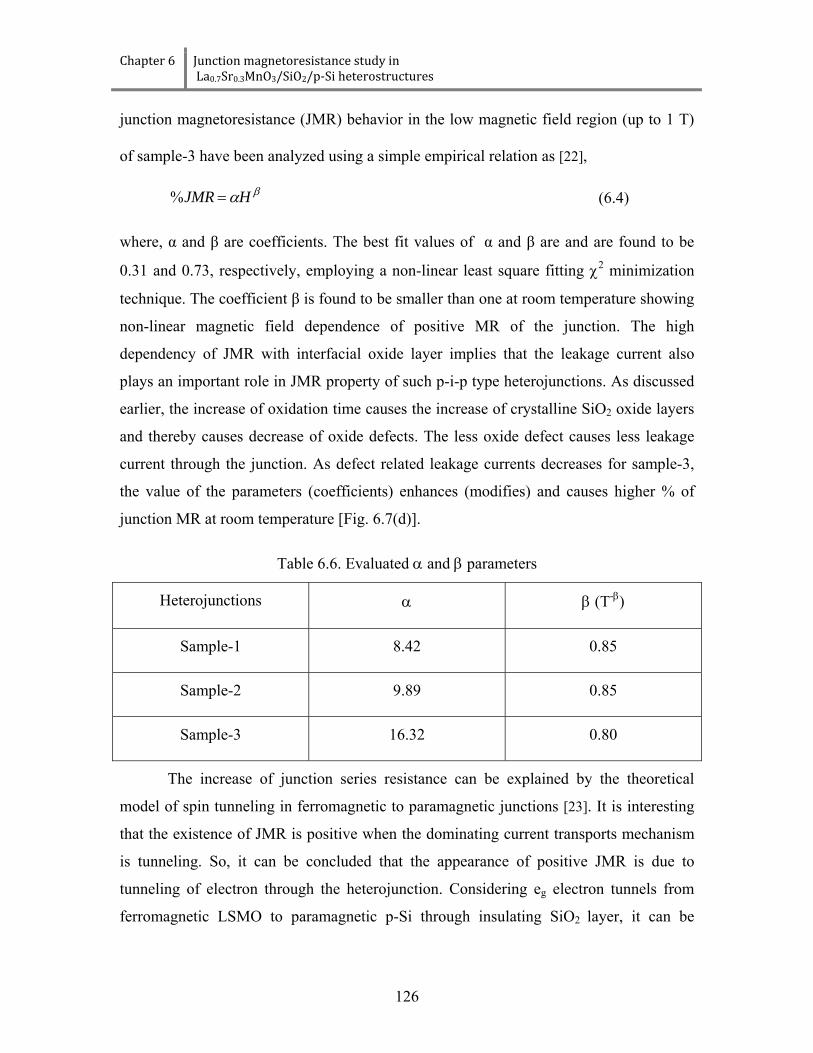
Chapter 6 Junction magnetoresistance study in La0.7Sr0.3MnO3/SiO2/p‐Si heterostructures
126
junction magnetoresistance (JMR) behavior in the low magnetic field region (up to 1 T)
of sample-3 have been analyzed using a simple empirical relation as [22],
βαHJMR =% (6.4)
where, α and β are coefficients. The best fit values of α and β are and are found to be
0.31 and 0.73, respectively, employing a non-linear least square fitting χ2 minimization
technique. The coefficient β is found to be smaller than one at room temperature showing
non-linear magnetic field dependence of positive MR of the junction. The high
dependency of JMR with interfacial oxide layer implies that the leakage current also
plays an important role in JMR property of such p-i-p type heterojunctions. As discussed
earlier, the increase of oxidation time causes the increase of crystalline SiO2 oxide layers
and thereby causes decrease of oxide defects. The less oxide defect causes less leakage
current through the junction. As defect related leakage currents decreases for sample-3,
the value of the parameters (coefficients) enhances (modifies) and causes higher % of
junction MR at room temperature [Fig. 6.7(d)].
Table 6.6. Evaluated α and β parameters
Heterojunctions α β (T-β)
Sample-1 8.42 0.85
Sample-2 9.89 0.85
Sample-3 16.32 0.80
The increase of junction series resistance can be explained by the theoretical
model of spin tunneling in ferromagnetic to paramagnetic junctions [23]. It is interesting
that the existence of JMR is positive when the dominating current transports mechanism
is tunneling. So, it can be concluded that the appearance of positive JMR is due to
tunneling of electron through the heterojunction. Considering eg electron tunnels from
ferromagnetic LSMO to paramagnetic p-Si through insulating SiO2 layer, it can be

Junction magnetoresistance in La0.7Sr0.3MnO3/SiO2/p‐Si heterostructures
Chapter 6
127
considered that there exist two channels (spin up I↑ and spin down I↓) at conduction band
for eg electrons to tunnel as shown in Fig. 6.11.
The ratio I↑/I↓ is proportional to the spin polarization of LSMO (Fig. 6.11). At room
temperature the ratio is approximately 1 due to the lower spin polarization of LSMO. The
both channels have allowed states at Fermi energy level and the both channels act in
tunneling mechanism at room temperature in absence of magnetic field. If the external
magnetic field is applied, the disordered spins are suppressed and the I↑/I↓ ratio increases.
One channel becomes inactive due to applied magnetic field and at Fermi energy level
only the other channel will have allowed states for tunneling at room temperature and low
temperatures. This reduces the current at a particular biasing field in presence of 1 T
magnetic field as observed in the J-V characteristics of the heterojunction. It most likely
causes enhancement of junction resistance under applied magnetic field.
The slight decrease of turn-on voltage with applied magnetic field shown in Fig.
6.3 and Fig. 6.8 implies that there is a certain voltage region in which the junction MR is
negative. This voltage region lies between the turn-on voltage and saturation voltage for
corresponding temperatures. The % of JMR plot with temperature has been shown in Fig.
6.12. The % JMR for all three samples decreases sharply with increasing the temperature.
Fig. 6.11. Schematic diagram of spin tunneling from magnetic LSMO to non magnetic Si with and without applied magnetic field.

Chapter 6 Junction magnetoresistance study in La0.7Sr0.3MnO3/SiO2/p‐Si heterostructures
128
With increasing of thermal energy it is more likely that the spin polarization decreases
and hence the change of junction resistance decreases. It causes the decrease of % JMR
with increasing temperature.
The change of junction MR with different forward bias voltages for all the three
samples at room temperature and for different temperatures for sample-3 have been
shown in Fig. 6.13(a) and Fig. 6.13(b), respectively.
The positive junction MR occurs at higher voltages and increases almost exponentially
with increasing forward bias voltages for all samples at all temperatures. In lower bias
Fig. 6.12. The temperature dependent junction MR plots for all three samples; the JMR has been calculated from the values of series resistances with and without 1 T magnetic field which are evaluated from the fitting of J-V curves.
120 160 200 240 280 3205
101520253035404550
Sample-1 Sample-2 Sample-3
% J
MR
Temperature (K)
2 3 4 5 60
4
8
12
16
20
24
Sample-1 Sample-2 Sample-3
% J
MR
Applied voltage (V)
T = 300 K
1 10
10
20
30
40
50
120 K 250 K 300 K
% J
MR
Applied Voltage (V)
Sample 3
Fig. 6.13. (a) The % of junction MR plot with applied bias voltage for all three samples. (b) The same plot for different temperature for sample-3.

Junction magnetoresistance in La0.7Sr0.3MnO3/SiO2/p‐Si heterostructures
Chapter 6
129
voltage regions (voltage lies between turn-on voltage and saturation voltage) the junction
shows either no such significant change in junction MR or negative junction MR for
different samples. The negative junction MR in this region becomes prominent at low
temperatures rather than room temperatures. It may be due to the effect of leakage current
through the junction. The leakage current is higher at room temperatures and there is no
such significant effect of magnetic field on leakage current which has been found through
this study. The little change of junction current may be compensated with leakage current
and overall current change can vanish at room temperature. When temperature decreases
the leakage current also decreases. The current change through the junction becomes
prominent at low temperatures.
6.4. Summary
In summary, we have successfully grown the LSMO/SiO2/p-Si heterostructure by
pulsed laser deposition technique and investigated its junction properties in details. We
have varied the SiO2 barrier layers thickness by varying oxidation times on cleaned Si
substrates. The various oxidation conditions are responsible for generating defects in
oxide layer which most likely play important role in carrier transport through the
junction. The dominating current transport mechanism through the junction is
temperature dependent Frenkel-Poole type emission. We have thoroughly investigated
the dependency of positive junction MR with applied biasing potentials and temperatures.
We have also found that the junction MR also depends on the defects induced leakage
current through the junction. The junction MR increases with increasing the thickness of
the SiO2 interfacial layer. It can be concluded that the leakage current can damage the
magnetic sensitivity (decrease of junction MR) of such devices. We have also estimated
the junction parameters such as ideality factor, turn-on voltages, barrier heights, series
resistances etc. It is found that the ideality factor, barrier height and series resistance
increase and turn-on voltages slightly decreases with the increase of external applied
magnetic field at all operating temperatures for all three samples. These results reveal that
the junction MR is positive at higher potentials and shows little negative value at lower
biasing voltage regions. Highest junction MR for the sample-3 has been found to be
~56% at 120 K and ~17% at 300 K at an applied bias voltage of 2 T. The thorough
Chapter 6 Junction magnetoresistance study in La0.7Sr0.3MnO3/SiO2/p‐Si heterostructures
130
analysis of junction J-V characteristics also leads to conclude that the arising of positive
MR at the junction is mainly due to the change of series resistances under magnetic field
rather than the change of effective barrier heights. We have also tried to establish
possible mechanism of the observed experimental results from our oxide thickness layer
dependent heterojunction employing the possible model of FM semiconductor/NM
semiconductor tunneling junction.
References
[1] S. Datta and B. Das, Electronic analog of the electro‐optic modulator, Appl. Phys. Lett. 56, 665 (1990). [2] J. Fontcuberta, L. Balcells, M. Bibes, J. Navarro, C. Frontera, J. Santiso, J. Fraxedas, B. Martínez, S. Nadolski, M. Wojcik, E. Jedryka and M J, Casanove, Magnetoresistive oxides: new developments and applications, J. Magn. Magn. Mat. 242, 98 (2002). [3] Y. Ishii, H. Yamada, H. Sato, H. Akoh, M. Kawasaki, Y. Tokura and Y. Tokura, Perovskite manganite magnetic tunnel junctions with enhanced coercivity contrast, Appl. Phys. Lett. 87, 022509 (2005). [4] R. S. Popovic, Not-plate-like Hall magnetic sensors and their applications, Sens. Act. A 85, 9 (2000). [5] M. Johnson, Magnetoelectronics, Academic Press, Elsevier, London,(2004). [6] J. Xing, K. Zhao , G. Z. Liu, M. He, K. J. Jin and H. B. Lu, Enhancement of photovoltaic effect in La0.9Sr0.1MnO3/Si heterojunction by side illumination, J. Phys. D: Appl. Phys. 40 5892 (2007). [7] K. Zhao, K. J. Jin, H. Lu, Y. Huang, Q. Zhou, M. He, Z. Chen, Y. Zhou and G. Yang, Transient lateral photovoltaic effect in p-n heterojunctions of La0.7Sr0.3MnO3 and Si, Appl. Phys. Lett. 88, 141914 (2006). [8] Lord K, Hunter D, Williams T M and Pradhan A K, Photocarrier injection effect and p-n junction characteristics of La0.7Sr0.3MnO3/ZnO and Si heterostructures, Appl. Phys. Lett. 89, 052116 (2006). [9] R. L. Zhang, W. H. Song, Y. Q. Ma, J. Yang, B. C. Zhao, G. H. Zheng, Z. G. Sheng, W. J. Lu and Y. P. Sun, The response for magnetic field, current and photo irradiation of charge-ordering LaSr2Mn2O7 thin film, J. Phys. D: Appl. Phys. 39 621 (2006). [10] S. J. May and B. W. Wessels, High-field magnetoresistance in p-(In,Mn)As/n-InAs heterojunctions, Appl. Phys. Lett. 88, 072105 (2006). [11] G. Chakraborty, S. Chattopadhyay, C. K. Sarkar, and C. Pramanik, Tunneling current at the interface of silicon and silicon dioxide partly embedded with silicon nanocrystals in metal oxide semiconductor structures, J. Appl. Phys. 101, 024315 (2007). [12] S. D. Ganichev, E. Ziemann, W. Prettl, I. N. Yassievich, A. A. Istratov and E. R. Weber, Distinction between the Poole-Frenkel and tunneling models of electric-field-stimulated carrier emission from deep levels in semiconductors, Phys. Rev. B 61, 10361 (2000). [13] G. Vincent, A. Chantre, and D. Bois, Electric field effect on the thermal emission of traps in semiconductor junctions, J. Appl. Phys. 50, 5484 (1979).

Junction magnetoresistance in La0.7Sr0.3MnO3/SiO2/p‐Si heterostructures
Chapter 6
131
[14] W. R. Buchwald, N. M. Johnson, Revised role for the Poole-frenkel effect in deep-level characterization, J. Appl. Phys. 64, 958 (1988). [15] L.Tsybeskov, G. F. Grom, P. M. Fauchet, J. P. McCaffrey, J. M. Baribeau, G. I. Sproule, and D. J. Lockwood , Phonon-assisted tunneling and interface quality in nanocrystalline Si/amorphous SiO2 superlattices, Appl. Phys. Lett. 75, 2265 (1999). [16] G. Vincent, A. Chantre, and D. Bois, Electric field effect on the thermal emission of traps in semiconductor junctions, J. Appl. Phys. 50, 5484 (1979). [17] F. D. Auret, S. A. Goodman, and W. E. Meyer, Electric-field-enhanced emission from radiation-induced hole traps in p-GaAs, Semicond. Sci. Technol. 10, 1376 (1995). [18] A. Ilie and B. Equer, Field-enhanced generation in hydrogenated amorphous silicon, Phys. Rev. B 57, 15349 (1998). [19] W. R. Buchwald and N. M. Johnson, Revised role for the Poole-frenkel effect in deep-level characterization, J. Appl. Phys. 64, 958 (1988). [20] P. A. Martin, B. G. Streetman and K. Hess, Electric field enhanced emission from non-Coulombic traps in Semiconductors, J. Appl. Phys. 52, 7409 (1981). [21] H. Zhang, E. J. Miller and E. T. Yua, Analysis of leakage current mechanisms in Schottky contacts to GaN and Al0.25Ga0.75N/GaN grown by molecular-beam epitaxy, J. Appl. Phys. 99, 023703 (2006). [22] Z. G. Sheng, W. H. Song, Y. P. Sun, J. R. Sun and B. G. Shen, Crossover from negative to positive magnetoresistance in La0.7Ce0.3MnO3-SrTiO3-Nb heterojunctions, Appl. Phys. Lett. 87, 032501 (2005). [23] I. Žutić, J. Fabian, and S. Das Sarma, Spintronics: Fundamentals and applications, Rev. Mod. Phys. 76, 323 (2004).

Chapter 7
Electronic-and magneto transport of
La0.7Sr0.3MnO3/ZnO, La0.7Sr0.3MnO3/Zn(Fe)O and
La0.7Sr0.3MnO3/Zn(Fe,Al)O heterostructures
This chapter is based on
International journals 1. Enhanced temperature dependent junction magnetoresistance in the heterojunctions with La0.7Sr0.3MnO3 and iron
doped ZnO carrier induced dilute magnetic semiconductors by S. Chattopadhyay, J. Panda, T. K. Nath, Journal of Applied Physics. (Communicated)
Conferences/Symposia 1. Temperature dependent junction magnetoresistance behavior of LSMO/Zn(Fe,Al)O heterojunction for spintronics by
J. Panda, S. Chattopadhyay and T. K. Nath, 55th DAE Solid State Physics Symposium 2010 (2010).

Electronic‐and magneto transport of La0.7Sr0.3MnO3/ZnO, La0.7Sr0.3MnO3/Zn(Fe)O and La0.7Sr0.3MnO3/Zn(Fe,Al)O heterostructures
Chapter 7
132
7.1. Introduction
In recent time, a great interest in the field of spintronics devices widely deals with several
kind of Schottky and heterojunctions of ferromagnetic materials/semiconductors with other non
magnetic semiconductors. Since the rediscovery of colossal magnetoresistance (CMR) effect in
manganite thin films, much attention has been focused on the fabrication of artificially designed
structures [1-3], such as magnetic tunnel junctions, and p–n junctions [4-7] to verify device
concepts based on oxide materials. The doped manganite La1−xAxMnO3 (A=Ca, Sr, and Ba) is a
strongly correlated-electron system with charge, orbital, spin, and lattice degrees of freedom,
possessing diverse physical phenomena. The heterostructures based on p-type perovskite oxides
show some special characteristics such as high magnetic sensitivity, ultraviolet photo voltage,
current field modulations, and the photo carrier injection effect [8-9]. The La0.7Sr0.3MnO3
(LSMO) is a typical double exchange highly spin-polarized system with a high Curie
temperature of about 360 K due to its large one-electron bandwidth. Therefore, it is one of the
best choices as a ferromagnetic electrode. On the other hand, ZnO is an n-type semiconductor
with a wide band gap and large exciton binding energy. However, there have been only a few
reports on the effect of magnetic fields on transport properties in LSMO/ZnO p-n
heterostructures [10,11]. On the other hand ZnO doped with transition metals shows room
temperature ferromagnetic properties, which is also called the dilute magnetic semiconductor
(DMS). With carrier concentration much smaller than the magnetic impurity concentration, the
DMS system provides a complimentary limit to Kondo system. The coupling between localized
impurity spin (S) and mobile valence band holes or conduction band electron can be represented
by the exchange interaction – J S.σ, where σ is the fermion spin operator. The Fe doped ZnO
shows room temperature ferromagnetic behavior and incorporating 1% Al shows enhanced
carrier induced ferromagnetism mainly due to the increase of charge carrier concentrations [12].
A few research work have been carried out with heterojunction of carrier induced ferromagnetic
n-type ZnO DMS with ferromagnetic half metallic p-type LSMO [13]. But a detail study
(thorough investigation) of spin injection through such p-n heterojunction is necessary for
complete understanding to use it in proper spintronics device applications.
In this chapter, we have demonstrated a detail junction magnetoresistive properties of
LSMO/ZnO, LSMO/Zn(Fe)O and LSMO/Zn(Fe,Al)O with different Fe concentrations (5, 7, and

Chapter 7 Electronic‐and magneto transport of La0.7Sr0.3MnO3/ZnO, La0.7Sr0.3MnO3/Zn(Fe)O and La0.7Sr0.3MnO3/Zn(Fe,Al)O heterostructures
133
10%) and established the temperature dependent spin injection and spin extraction process
through the junction.
7.2. Experimental Procedure
7.2.1. Preparation of target
The LSMO powder was synthesized through chemical pyrophoric reaction process where
we have employed stoichiometric mixtures of high purity La2O3 (99.99 %), SrCO3 (99.9+ %) and
Mn(CH3COO)2 (99.0 %). After final grinding and pelletization of LSMO powders, the pelletized
sample was first heated at 800 °C for 12 h, then at 1000 °C for 12 h and at 1200 °C for another
12 h, with intermediate grinding. Final sintering of the LSMO target was carried out at 1200 °C
for 24 h.
The iron doped ZnO powder was first synthesized by solid state reaction process.
Required amount of high purity ZnO, Fe2O3 powder were well mixed with hand grinder
repeatedly and sintered at 450 ºC till the required phase appeared. Required amount of Al2O3
powder were mixed with the ZnO and Fe2O3 powder to dope 1% aluminum in Zinc iron oxide
target. Finally, the Zn(Fe)O and Zn(Fe,Al)O powders were pelletized and sintered at 450 ºC to
use it as the target for pulsed laser deposition (PLD).
7.2.2. Cleaning of substrate
The c-plane (0001) sapphire substrate has been cleaned repeatedly with De-ionized water,
Acetone and Propanol using ultrasonic vibrator. Each cleaning method has been carried out for
20 min.
7.2.3. Preparation of heterojunction
At first the LSMO film was deposited on (0001) well cleaned sapphire substrate at 800 oC and 0.5 mbar O2 pressure. The laser pulse (248 nm KrF laser) of energy density 4 J/cm2 was
applied on the LSMO target for 20 min at a frequency of 10 Hz. The substrate to target distance
was kept at 4 cm in the chamber. After deposition, the film was sintered at the same physical
condition for 1 hr to get well crystalline samples. Then a portion of the substrates were masked
and the ZnO films were grown on the LSMO. The films were grown on LSMO at a substrate
temperature at 450 oC and in ambient oxygen pressures at 10-5 Torr. The excimer laser was used

Electronic‐and magneto transport of La0.7Sr0.3MnO3/ZnO, La0.7Sr0.3MnO3/Zn(Fe)O and La0.7Sr0.3MnO3/Zn(Fe,Al)O heterostructures
Chapter 7
134
for 30 min at a laser pulse frequency (repetition rate) of 10 Hz. Electrical contacts were made
with high purity Ag on LSMO film and highly pure In contact with ZnO as ohmic contacts.
7.2.4. Characterization of heterostructure
The structural and surface morphological studies have been carried out using high
resolution x-ray diffraction (Philips pan analytical x-pert), scanning electron microscope (Carl
Zeiss) and atomic force microscope (Nanonics). The electrical properties have been studied out
in details using Keithley 2612 source meter with 1 microvolt resolution and a DMM (Keithley-
2000) along with a temperature controller (Lakeshore-330). The magnetic field was applied in
the current parallel to the plane (CPP) geometry with the magnetic field parallel to the film plane
using a high precision electromagnet (polytronic, model HEM 100).
7.3. Results and Discussion
7.3.1. Structural and surface study
Fig. 7.1.(a) High resolution XRD pattern of LSMO/ZnO heterojunction on sapphire substrate. (b) Zoomed view of HRXRD along with Gaussian fit of (110) plane of LSMO and(201) plane of ZnO(inset). (c) and (d) are the FESEM image of surface and cross sectional view, respectively.
30 31 32 33 34 35
64 66 68 70 72 74 76
Inta
nsity
(a.u
)
2θ(Degree)
2θ
(b)
Inte
nsity
(a.u
)
20 30 40 50 60 70 80
Inte
nsity
(a.u
)
2θ (Degree)
LSM
O (1
0 0
) LSM
O (1
1 0
)Z
nO (1
0 1
) LSM
O (1
1 1
)A
l 2O3 (0
0 6
)Z
nO (1
0 2
)
ZnO
(2 0
1)
(a)
(c)
100 nm
LSMO
ZnO
(d)
200 nm

Chapter 7 Electronic‐and magneto transport of La0.7Sr0.3MnO3/ZnO, La0.7Sr0.3MnO3/Zn(Fe)O and La0.7Sr0.3MnO3/Zn(Fe,Al)O heterostructures
135
The high resolution x-ray diffraction (HRXRD) pattern, shown in Fig. 7.1(a), has been
carried out using Cu-Kα radiation. Both LSMO film and ZnO films show non-epitaxial behavior
on (0001) c-plane sapphire substrate. The growth of LSMO is in the directions of (100), (110)
and (111) plane and ZnO is in the direction of (101), (102) and (201) planes have been found.
Figure 7.1(b) shows the zoomed view of LSMO (110) and ZnO (201) planes (inset of Fig.
7.1(b)) along with Gaussian fit. It gives the lattice parameters LSMO and ZnO (aLSMO ~ 3.83 Å
and aZnO ~ 3.53 Å). In Fig. 7.1(c) and 7.1(d), the FESEM micrograph of the top view of one of
the LSMO/ZnO heterojunction and the cross sectional FESEM image of the heterojunction have
been shown, respectively. The FESEM micrograph clearly shows the uniformly grown smooth
LSMO and ZnO film with good coverage on sapphire substrate. The average thickness of the
LSMO layer is around ~ 371 nm and ZnO layer is around ~ 124 nm.
Figures 7.2(a) and (b) show the atomic force microscopic (AFM) image of the surface of
LSMO film on (0001) sapphire substrate and 3-d view of the LSMO film, respectively. The
r.m.s. roughness of the LSMO film is found to be ~2 nm. The AFM scan at the junction has been
taken and their 2-d and 3-d image of the junction has been shown in Fig. 7.2(c) and (d),
Fig. 7.2. AFM image of LSMO surface morphology: (a) 2-d and (b) 3-d view. AFM image of LSMO/ZnO heterojunction: (c) 2-d and (d) 3-d view.
0.03 Volts
-0.04 Volts
1.0µm
0.97 Volts
-0.43 Volts
1.20 Volts
-0.47 Volts
1.0µm
(a(b)
(c) (d)

Electronic‐and magneto transport of La0.7Sr0.3MnO3/ZnO, La0.7Sr0.3MnO3/Zn(Fe)O and La0.7Sr0.3MnO3/Zn(Fe,Al)O heterostructures
Chapter 7
136
respectively. From the image contrast in Fig. 7.2(d) it is clear that the ZnO layer has been grown
on LSMO film and it confirms the formation of heterojunction.
7.3.2. Electrical properties study
The room temperature current density-voltage (J-V) properties of ZnO/LSMO,
Zn(Fe)O/LSMO and Zn(Fe,Al)/LSMO heterojunctions with 5% Fe have been shown in Fig. 7.3.
Insets (a) and (b) of Fig. 7.3 are the isothermal LSMO/Ag and ZnO/In ohmic contacts,
respectively measured at several different temperatures. These metallic contacts are linear in all
temperatures which confirm that the non linearity of J-V properties originates from ZnO/LSMO
junctions only, not from metal - semiconductor contacts. Doping with 1% Al enhances the carrier
concentration of ZnO films (~1022 /cm3) and causes a very thin depletion layer across the
heterojunctions. So, the reverse saturation current becomes very high and does not show good
rectifying behavior where as ZnO/LSMO, Zn(Fe)O/LSMO shows reasonably good rectifying
behavior as the films have moderate carrier concentrations (~1019-1021/cm3). Large current flows
through the Zn(Fe,Al)O/LSMO junction rather than the ZnO/LSMO or Zn(Fe)O/LSMO
heterojunctions.
Fig. 7.3. Room temperature J-V properties of LSMO/ZnO, LSMO/Zn(Fe)O and LSMO/Zn(Fe,Al)O heterojunction. Upper inset shows the ohmic nature of I-V behavior for LSMO-Ag electrical contact at several temperatures (77-300 K). Lower inset shows the same for ZnO-In electrical contact.
-5 -4 -3 -2 -1 0 1 2 3 4 5
-100
-50
0
50
100
ZnO
Zn(Fe)O
Cur
rent
(mA
/cm
2 )
Voltage(V)
Zn(Fe,Al)O
-3 -2 -1 0 1 2 3-0.4
-0.2
0.0
0.2
0.4 77 K 100 K 150 K 200 K 250 K 300 K
Cur
rent
(mA
)
Voltage (V)
LSMO/AgOhmic contact
(a)
-4 -3 -2 -1 0 1 2 3 4-15
-10
-5
0
5
10
15
(b)
77 K 100 K 150 K 200 K 250 K 300 K
Cur
rent
(mA
)
Voltage (V)
ZnO/InOhmic contact

Chapter 7 Electronic‐and magneto transport of La0.7Sr0.3MnO3/ZnO, La0.7Sr0.3MnO3/Zn(Fe)O and La0.7Sr0.3MnO3/Zn(Fe,Al)O heterostructures
137
Figure 7.4(a) shows the J-V behavior of Zn(Fe)O/LSMO junction with different Fe
doping percentages ranging from 0 to 10%. Figure 7.4(b) is the J-V behavior of
Zn(Fe,Al)O/LSMO junction with different percentages. The junction J-V characteristics can be
described as [14],
⎟⎟⎠
⎞⎜⎜⎝
⎛ −=
kTJARVe
JJ s
η)(
exp0 (7.1)
where, J0 is the reverse saturation current density. η and Rs are, the ideality factor and junction
series resistance, respectively. A is the junction area. The parameters evaluated from the forward
J-V curves of all those films have been summarized in Table 7.1. The little increase of junction
series resistance with increasing doping concentration reveals the lowering of carrier
concentration in Zn(Fe)O and Zn(Fe,Al)O films.
Figure 7.5(a) shows the temperature dependent J-V characteristics of LSMO/ZnO
heterojunction. Figures 7.5(b), (c) and (d) are the temperature dependent J-V characteristics of
LSMO/Zn(Fe)O heterojunctions with 5, 7, 10% iron doping, respectively. Accordingly, Fig.
7.6(a), (b) and (c) are the junction J-V characteristics of LSMO/Zn(Fe,Al)O with 5, 7 and 10%
Fe. All parameters evaluated from the fitting using Eq. (7.1) have been listed in Table 7.1. The
temperature dependent series resistance for the LSMO/ZnO, LSMO/Zn(Fe)O and
LSMO/Zn(Fe,Al)O junctions with 5% Fe doping have been shown in Fig. 7.6(d). The junction
series resistance is found to decrease with increasing temperature which is generally expected in
p-n junction characteristics.
Fig. 7.4. Room temperature J-V properties of (a) LSMO/ZnO, LSMO/Zn(Fe)O and (b) LSMO/Zn(Fe,Al)O heterojunction with different Fe concentrations.
-8 -6 -4 -2 0 2 4 6-10-505
101520253035
Cur
rent
(mA
/cm
2 )
Voltage (V)
300 KLSMO/Zn(Fe)O
0%5%
7%
10%
H=0 T
(a)-3 -2 -1 0 1 2 3
-100
-50
0
50
100
(b)
Cur
rent
(mA
/cm
2 )
Voltage(V)
5%
10%
7% 300 KLSMO/Zn(Fe,Al)O
H=0 T

Electronic‐and magneto transport of La0.7Sr0.3MnO3/ZnO, La0.7Sr0.3MnO3/Zn(Fe)O and La0.7Sr0.3MnO3/Zn(Fe,Al)O heterostructures
Chapter 7
138
Fig.7.5. (a) J-V properties of LSMO/ZnO heterojunction at different isothermal temperatures, (b), (c) and (d) are the same plots for LSMO/Zn(Fe)O heterostructures with 5, 7 and 10% Fe concentrations, respectively.
-10 -5 0 5-10-505
101520253035
77 K100 K
150 K200 K
250 K
Cur
rent
(mA
/cm
2 )
Voltage (V)
300 K
LSMO/ZnO
(a)
H=0 T
-10 -8 -6 -4 -2 0 2 4 6-10-505
1015202530
77 K
100 K150 K
200 K
250 K
Cur
rent
(mA
/cm
2 )
Voltage (V)
300 K
LSMO/Zn(Fe)Owith 5% Fe
(b)
H=0 T
-10 -8 -6 -4 -2 0 2 4 6-10
-5
0
5
10
15
20
25
77 K
100 K
150 K
200 K
250 K
Cur
rent
(mA
/cm
2 )
Voltage (V)
300 K
LSMO/Zn(Fe)Owith 7%
(c)
H=0 T
-10 -8 -6 -4 -2 0 2 4 6
-5
0
5
10
15
20
100 K
150 K
200 K
250 K
Cur
rent
(mA
/cm
2 )
Voltage (V)
300 K
LSMO/Zn(Fe)Owith 10% Fe
(d)
H=0 T
77 K
Fig. 7.6. (a) J-V properties of LSMO/ZnO heterojunction at different isothermal temperatures, (b), (c) and (d) are the same plots for LSMO/Zn(Fe)O heterostructures with 5, 7 and 10% Fe concentrations, respectively.
50 100 150 200 250 300
0.0
0.5
1.0
1.5
2.0
2.5
3.0
ZnO ZnFeO ZnFeAlO
Rs (Ω
-cm
2 )
Temperature (K)
With out field
(d)
-3 -2 -1 0 1 2 3
-100
-50
0
50
100
77 K 100 K 150 K 200 K 250 K 300 K
Cur
rent
(mA
/cm
2 )
Voltage(V)
LSMO/Zn(Fe,Al)O5% Fe
(a)
H=0 T
-3 -2 -1 0 1 2 3-100-80-60-40-20
020406080
100
77 K 100 K 150 K 200 K 250 K 300 K
H=0 T
Cur
rent
(mA
/cm
2 )
Voltage(V)
Zn(Fe,Al)O7% Fe
(b)
-3 -2 -1 0 1 2 3-80-60-40-20
020406080
77 K 100 K 150 K 200 K 250 K 300 K
H=0 T
Cur
rent
(mA
/cm
2 )
Voltage(V)
Zn(Fe,Al)O10% Fe
(c)
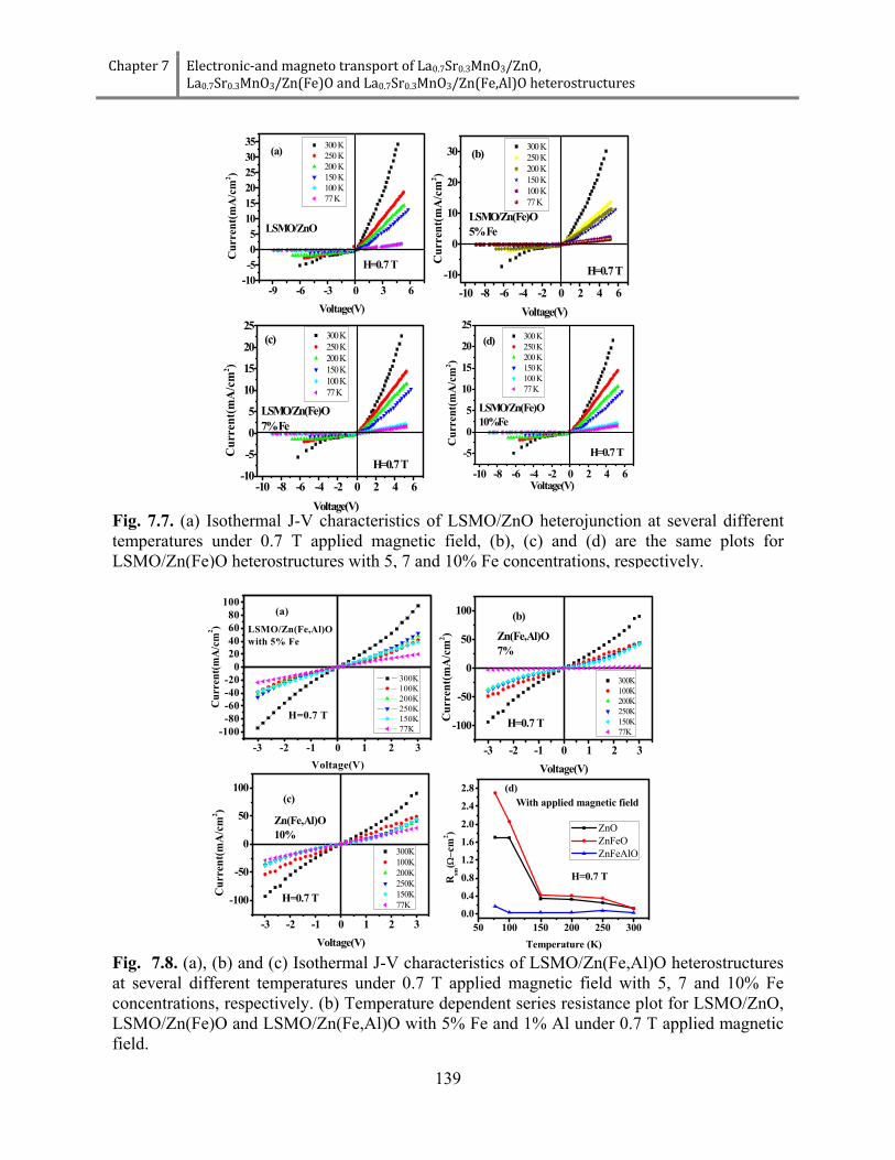
Chapter 7 Electronic‐and magneto transport of La0.7Sr0.3MnO3/ZnO, La0.7Sr0.3MnO3/Zn(Fe)O and La0.7Sr0.3MnO3/Zn(Fe,Al)O heterostructures
139
Fig. 7.7. (a) Isothermal J-V characteristics of LSMO/ZnO heterojunction at several different temperatures under 0.7 T applied magnetic field, (b), (c) and (d) are the same plots for LSMO/Zn(Fe)O heterostructures with 5, 7 and 10% Fe concentrations, respectively.
-9 -6 -3 0 3 6-10-505
101520253035
H=0.7 T
300 K 250 K 200 K 150 K 100 K 77 K
Cur
rent
(mA
/cm
2 )
Voltage(V)
LSMO/ZnO
(a)
-10 -8 -6 -4 -2 0 2 4 6-10
0
10
20
30
H=0.7 T
300 K 250 K 200 K 150 K 100 K 77 K
Cur
rent
(mA
/cm
2 )
Voltage(V)
LSMO/Zn(Fe)O5% Fe
(b)
-10 -8 -6 -4 -2 0 2 4 6-10
-5
0
5
10
15
20
25
H=0.7 T
300 K 250 K 200 K 150 K 100 K 77 K
Cur
rent
(mA
/cm
2 )
Voltage(V)
LSMO/Zn(Fe)O7% Fe
(c)
-10 -8 -6 -4 -2 0 2 4 6
-5
0
5
10
15
20
25 300 K 250 K 200 K 150 K 100 K 77 K
Cur
rent
(mA
/cm
2 )
Voltage(V)
LSMO/Zn(Fe)O10%Fe
(d)
H=0.7 T
50 100 150 200 250 3000.0
0.4
0.8
1.2
1.6
2.0
2.4
2.8
Rsm
(Ω−c
m2 )
Temperature (K)
ZnO ZnFeO ZnFeAlO
With applied magnetic field(d)
H=0.7 T
-3 -2 -1 0 1 2 3-100
-80-60-40-20
020406080
100
H=0.7 T
Cur
rent
(mA
/cm
2 )
Voltage(V)
300K 100K 200K 250K 150K 77K
(a)
LSMO/Zn(Fe,Al)Owith 5% Fe
-3 -2 -1 0 1 2 3
-100
-50
0
50
100
H=0.7 T
300K 100K 200K 250K 150K 77K
Cur
rent
(mA
/cm
2 )
Voltage(V)
Zn(Fe,Al)O7%
(b)
-3 -2 -1 0 1 2 3
-100
-50
0
50
100
H=0.7 T
300K 100K 200K 250K 150K 77K
Cur
rent
(mA
/cm
2 )
Voltage(V)
Zn(Fe,Al)O10%
(c)
Fig. 7.8. (a), (b) and (c) Isothermal J-V characteristics of LSMO/Zn(Fe,Al)O heterostructures at several different temperatures under 0.7 T applied magnetic field with 5, 7 and 10% Fe concentrations, respectively. (b) Temperature dependent series resistance plot for LSMO/ZnO, LSMO/Zn(Fe)O and LSMO/Zn(Fe,Al)O with 5% Fe and 1% Al under 0.7 T applied magnetic field.
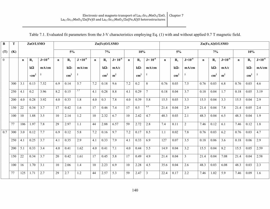
Electronic‐and magneto transport of La0.7Sr0.3MnO3/ZnO, La0.7Sr0.3MnO3/Zn(Fe)O and La0.7Sr0.3MnO3/Zn(Fe,Al)O heterostructures
Chapter 7
140
Table 7.1. Evaluated fit parameters from the J-V characteristics employing Eq. (1) with and without applied 0.7 T magnetic field.
B
(T)
T
(K)
ZnO/LSMO Zn(Fe)O/LSMO Zn(Fe,Al)O/LSMO
5% 7% 10% 5% 7% 10%
0 n Rs
kΩ
-cm2
J×10-6
mA/cm
2
n Rs
kΩ-
cm2
J ×10-6
mA/cm
2
n Rs
kΩ-
cm2
J× 10-6
mA/c
m2
n Rs
kΩ-
cm2
J× 10-6
mA/cm
2
n Rs
kΩ-
cm2
J×10-6
mA/cm
2
n Rs
kΩ-
cm2
J×10-6
mA/c
m2
n Rs
kΩ-
cm2
J×10-6
mA/cm
2
300 3.1 0.13 7.52 6.9 0.14 5.7 7.2 0.18 9.6 7.2 0.2 8 0.76 0.03 7.5 0.76 0.03 6.8 0.76 0.03 4.6
250 4.1 0.2 3.96 8.2 0.15 3.7 4.1 0.28 8.8 4.1 0.29 7 0.18 0.04 3.7 0.18 0.04 1.7 0.18 0.05 3.19
200 4.0 0.28 3.92 4.0 0.33 1.8 4.0 0.3 7.8 4.0 0.39 5.8 15.5 0.03 3.3 15.5 0.04 3.3 15.5 0.04 2.9
150 22 0.34 3.7 17 0.42 1.6 17 0.46 7.4 17 0.5 4.9 21.4 0.04 2.9 21.4 0.04 7.8 21.4 0.05 2.4
100 10 1.88 3.5 10 2.14 1.2 10 2.32 6.7 10 2.42 4.7 48.3 0.03 2.1 48.3 0.04 6.5 48.3 0.04 1.9
77 106 1.97 7.8 29 2.97 1.1 44 2.88 6.57 59 2.72 2.8 7.4 0.11 2 7.46 0.12 6.1 7.46 0.12 1.8
0.7 300 3.0 0.12 7.7 6.9 0.12 5.8 7.2 0.16 9.7 7.2 0.17 8.5 1.1 0.02 7.8 0.76 0.03 6.2 0.76 0.03 4.7
250 4.1 0.25 3.7 4.1 0.35 2.9 4.1 0.33 7.9 4.1 0.33 6.9 127 0.07 3.5 0.18 0.06 3.6 0.18 0.06 2.9
200 5.1 0.33 3.4 4.0 0.41 1.62 4.0 0.41 7.1 4.0 0.44 5.5 14.9 0.04 3.2 15.5 0.04 8.2 15.5 0.05 2.59
150 22 0.34 3.7 20 0.42 1.61 17 0.45 5.8 17 0.49 4.9 21.4 0.04 3 21.4 0.04 7.08 21.4 0.04 2.58
100 16 1.70 3.1 10 2.06 1.4 10 2.23 6.9 10 2.28 4.5 35.6 0.04 2.6 48.3 0.03 6.08 48.3 0.03 2.3
77 125 1.71 2.7 29 2.7 1.2 44 2.57 5.3 59 2.47 3 22.4 0.17 2.2 7.46 1.02 5.9 7.46 0.09 1.6

Chapter 7 Electronic‐and magneto transport of La0.7Sr0.3MnO3/ZnO, La0.7Sr0.3MnO3/Zn(Fe)O and La0.7Sr0.3MnO3/Zn(Fe,Al)O heterostructures
141
Figure 7.7(a) shows the temperature dependent J-V characteristics of LSMO/ZnO
heterojunction under 0.7 T applied magnetic field. Figures 7.7(b), (c) and (d) are the temperature
dependent J-V characteristics of LSMO/Zn(Fe)O heterojunctions with 5, 7, 10% iron doping,
respectively under 0.7 T applied magnetic field. Figures 7.8(a), (b) and (c) are the junction J-V
characteristics of LSMO/Zn(Fe,Al)O with 5, 7 and 10% Fe doping under 0.7 T applied magnetic
field. The parameters in Eq. (7.1) are modified under magnetic field (J0, η and Rs are now
replaced by J0m, ηm and Rsm, respectively). The modified value of parameters evaluated
employing modified Eq. (7.1) has also been enlisted in Table 7.1. The temperature dependent
series resistance under 0.7 T magnetic field for the LSMO/ZnO, LSMO/Zn(Fe)O and
Zn(Fe,Al)O junctions with 5% Fe has been shown in Fig. 7.8(d). The junction series resistance
under magnetic field also decreases with increasing temperature.
7.3.3. Junction Magnetoresistance properties
Fig. 7.9. Comparative J-V characteristics of LSMO/ZnO (I), LSMO/Zn(Fe)O (II) and LSMO/Zn(Fe,Al)O (III) heterostructures with and without applied 0.7 T magnetic field. The Fe and Al concentration are 5% and 1%, respectively. (a), (b), (c) and (d) are the same J-V characteristics measured at 77, 200, 250 and 300 K, respectively.
I
II
III
I
II
III
I
II
III
I
II
III
(a) (b) (c) (d)
1 2 3 4 5 60.40.60.81.01.21.41.61.82.0
0T
Cur
rent
(mA
/cm
2 )
Voltage(V)
77 KZnO/LSMO
0.7T
1 2 3 4 5 62468
1012141618
Cur
rent
(mA
/cm
2 )
Voltage(V)
ZnO/LSMO at 200K
0.7T
0T
1 2 3 4 5 60
2
4
6
8
10
12
14
16
Voltage(V)
Cur
rent
(mA
/cm
2 )
ZnFeo/LSMO at 200K0T
0.7T
0.0 0.5 1.0 1.5 2.0 2.5 3.00
10
20
30
40
50
60
Cur
rent
(mA
/cm
2 )
Voltage(V)
ZnFeAl/LSMO at 200K
0.7T0T
0 1 2 3 4 5 60
5
10
15
20
25
Cur
rent
(mA
/cm
2 )
Voltage(V)
ZnO/LSMO at 250K
0.7T
0T
0 1 2 3 4 5 60
5
10
15
20
Cur
rent
(mA
/cm
2 )
Voltage(V)
ZnFeO/LSMO at 250K
0.7T
0T
0.0 0.5 1.0 1.5 2.0 2.5 3.00
10
20
30
40
50
60
70
Cur
rent
(mA
)
Voltage(V)
ZnFeAlO/LSMO at 250K
0.7T
0T
0 1 2 3 4 50
5
10
15
20
25
30
35
Cur
rent
(mA
/cm
2 )
Voltage(V)
ZnO/LSMO at 300K
0.7T
0T
0 1 2 3 4 50
5
10
15
20
25
30
35
Cur
rent
(mA
/cm
2 )
Voltage(V)
ZnFeO/LSMO at 300K
0.7T
0T
0.0 0.5 1.0 1.5 2.0 2.5 3.00
20
40
60
80
100
Cur
rent
(mA
/cm
2 )
Voltage(V)
ZnFeAlO/LSMO at 300K
0.7T0T
0 1 2 30
10
20
30
Cur
rent
(mA
/cm
2 )
Voltage(V)
ZnFeAl/LSMOat 77K0.7T
0T
0 1 2 3 4 5 60.00.20.40.60.81.01.21.41.61.8
Cur
rent
(mA
/cm
2 )
Voltage(V)
ZnFeO/LSMO 0.7T
0T

Electronic‐and magneto transport of La0.7Sr0.3MnO3/ZnO, La0.7Sr0.3MnO3/Zn(Fe)O and La0.7Sr0.3MnO3/Zn(Fe,Al)O heterostructures
Chapter 7
142
The detailed comparative study of J-V with and without applied 0.7 T magnetic field
measured at different temperatures (77, 200, 250 and 300 K) for LSMO/ZnO, LSMO/Zn(Fe)O
and Zn(Fe,Al)O heterojunctions with 5% Fe doping have been shown in Fig. 7.9. Figure 7.9(a I-
III) are the J-V characteristics at 77 K, Fig. 7.9(b I-III) are for 200 K, Fig. 7.9(c I-III) are for 250
K and Fig. 7.9(d I-III) for 300 K. It clearly demonstrates that all the heterojunctions show the
negative junction MR at 77 and 300 K and positive junction MR at 200 and 250 K.
The change of junction MR with applied magnetic fields up to 0.7 T for LSMO/ZnO,
LSMO/Zn(Fe)O, LSMO/Zn(Fe,Al)O heterojunctions with 5% Fe doping at a bias voltage of 3 V
has been shown in Fig. 7.10 (a), (b), (c) and (d) for 77, 200, 250 and 300 K, respectively. The
magnetic field dependent junction magnetoresistance (JMR) behavior in the magnetic field
region up to 0.7 T of LSMO/ZnO, LSMO/Zn(Fe)O and Zn(Fe,Al)O junctions with 5% Fe have
been analyzed using a simple empirical relation as [15],
Fig. 7.10. Plot of junction magnetoresistance with applied magnetic field at (a) 77 K, (b) 200 K, (c) 250 K and (d) 300 K of the LSMO/ZnO, LSMO/Zn(Fe)O and LSMO/Zn(Fe,Al)O heterojunctions with 5% Fe concentration at a bias voltage of 3 V.
(b)

Chapter 7 Electronic‐and magneto transport of La0.7Sr0.3MnO3/ZnO, La0.7Sr0.3MnO3/Zn(Fe)O and La0.7Sr0.3MnO3/Zn(Fe,Al)O heterostructures
143
βαHJMR = (7.2)
where, α and β are coefficients. The junction magnetoresistance behaviors of other doped
samples have also been investigated employing Eq. (7.2). The obtained best fit values of α and β
for LSMO/ZnO, LSMO/Zn(Fe)O and Zn(Fe,Al)O junctions with 5% Fe are listed in Table 7.2.
The exponent is found to be high (~1) at 200 K and it becomes ~0.5 at higher temperatures for
all these heterojunctions.
Table 7.2. Fit parameters (α and β) evaluated from Eq. (2) for undoped LSMO/ZnO, LSMO/Zn(Fe)O and LSMO/Zn(Fe)O with 5% Fe doping.
Sample Temperature (K) α β
ZnO 77 -7.5 0.27
200 3.1 0.82
250 8.4 0.53
300 -4.5 0.5
Zn(Fe)O 77 -4.7 0.39
200 4.2 0.83
250 13.4 0.53
300 -4.1 0.51
Zn(Fe,Al)O 77 -3.8 0.39
200 5.4 0.83
250 31.1 0.45
300 -0.72 0.51
The origin of junction magnetoresistances in those heterostructures can be best explained by the
spin injection theory of magnetic p-n junction. Spin injection generally occurs in n-side while
spin extraction generally occurs in p-side. Both spin injection and spin extraction becomes large
with applied magnetic field. The current through the magnetic p-n junction depends on magnetic
field because of the spin orbit splitting of magnetic materials [16]. The spin splitting of
conduction bands are created by doping with magnetic ions in non-magnetic semiconductors.
Doping with iron causes a large non equilibrium population of polarized electrons in ZnO
conduction band. This non equilibrium population at magnetic n-side enhances the spin injection
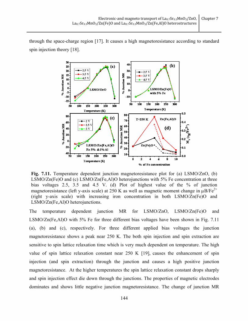
Electronic‐and magneto transport of La0.7Sr0.3MnO3/ZnO, La0.7Sr0.3MnO3/Zn(Fe)O and La0.7Sr0.3MnO3/Zn(Fe,Al)O heterostructures
Chapter 7
144
through the space-charge region [17]. It causes a high magnetoresistance according to standard
spin injection theory [18].
The temperature dependent junction MR for LSMO/ZnO, LSMO/Zn(Fe)O and
LSMO/Zn(Fe,Al)O with 5% Fe for three different bias voltages have been shown in Fig. 7.11
(a), (b) and (c), respectively. For three different applied bias voltages the junction
magnetoresistance shows a peak near 250 K. The both spin injection and spin extraction are
sensitive to spin lattice relaxation time which is very much dependent on temperature. The high
value of spin lattice relaxation constant near 250 K [19], causes the enhancement of spin
injection (and spin extraction) through the junction and causes a high positive junction
magnetoresistance. At the higher temperatures the spin lattice relaxation constant drops sharply
and spin injection effect die down through the junctions. The properties of magnetic electrodes
dominates and shows little negative junction magnetoresistance. The change of junction MR
Fig. 7.11. Temperature dependent junction magnetoresistance plot for (a) LSMO/ZnO, (b) LSMO/Zn(Fe)O and (c) LSMO/Zn(Fe,Al)O heterojunctions with 5% Fe concentration at three bias voltages 2.5, 3.5 and 4.5 V. (d) Plot of highest value of the % of junction magnetoresistance (left y-axis scale) at 250 K as well as magnetic moment change in μB/Fe2+ (right y-axis scale) with increasing iron concentration in both LSMO/Zn(Fe)O and LSMO/Zn(Fe,Al)O heterojunctions.

Chapter 7 Electronic‐and magneto transport of La0.7Sr0.3MnO3/ZnO, La0.7Sr0.3MnO3/Zn(Fe)O and La0.7Sr0.3MnO3/Zn(Fe,Al)O heterostructures
145
calculated at 250 K at 2.5 V applied bias voltage for different iron concentrations have been
shown in Fig. 7.11(d). The change of magnetic moment (MS) in Bohr magneton per Fe2+of both
Zn(Fe)O and Zn(Fe,Al)O films with doping percentage have also been shown in the Fig. 7.11(d)
[the dashed lines]. Both the magnetic moment per Fe2+ and junction MR decreases with increase
of Fe concentration. The drop of moment with increasing iron concentrations may be due to the
increasing of antiferromagnetic coupling between Fe pairs which occurs at shorter separation
distances and decrease the spin up population in DMS systems. The decrease of junction MR
with increasing iron concentrations in both Zn(Fe)O and Zn(Fe,Al)O system is most likely due to
the decrease of spin up population caused by higher doping.
7.4. Summary
LSMO/ZnO, LSMO/Zn(Fe)O and LSMO/Zn(Fe,Al)O heterojunctions with 5, 7 and 10%
Fe have been fabricated using pulsed laser deposition technique. The junction J-V properties
have been studied with and without applying magnetic field. The junction with ZnO and
Zn(Fe)O shows good rectifying behavior at all temperatures but heterojunctions with Zn(Fe,Al)O
shows a quick break down at reverse bias. Higher carrier concentration in Zn(Fe,Al)O most
likely causes thin depletion region and hence causes high current transport through the junction.
All the heterojunctions show high positive junction magnetoresistance at a certain temperature
range (150 to 280 K) and low negative magnetoresistance at 77 K and 300 K. The junction
magnetoresistance enhances due to incorporation of 1% Al. This has been best explained using
spin injection theory through magnetic p-n junction. Increase of Fe doping concentration
decreases the junction magnetoresistance as well as magnetic moment per Fe2+ for both Zn(Fe)O
and Zn(Fe,Al)O systems. This is mainly due to the decrease of population of polarized electron
in conduction band. The properties of junction magnetoresistance of such heterostructures can be
extremely useful in the area of spintronic devices.
References
[1] C. Mitra, P. Raychaudhuri, K. Do¨rr, K. H. Mu¨ller, L. Schultz, P.M. Oppeneer, and S.Wirth, Observation of Minority Spin Character of the New Electron Doped Manganite La0.7Ce0.3MnO3 from Tunneling Magnetoresistance, Phys. Rev. Lett. 90, 017202 (2003). [2] C. Mitra, G. Köbernik, K. Dörr, K. H. Müller, L. Schultz, P. Raychaudhuri, R. Pinto, and E. Wieser, Magnetotransport properties of a room temperature rectifying tunnel junction made of electron and hole doped manganites, J. Appl. Phys. 91, 7715 (2002).

Electronic‐and magneto transport of La0.7Sr0.3MnO3/ZnO, La0.7Sr0.3MnO3/Zn(Fe)O and La0.7Sr0.3MnO3/Zn(Fe,Al)O heterostructures
Chapter 7
146
[3] C. Mitra, P. Raychaudhuri, G. Köbernik, K. Dörr, K.-H. Müller, L. Schultz and R. Pinto, p-n diode with hole- and electron-doped lanthanum manganites, Appl. Phys. Lett. 79, 2408 (2001). [4] H. Tanaka, J. Zhang, and T. Kawai, Giant Electric Field Modulation of Double Exchange Ferromagnetism at Room Temperature in the Perovskite Manganite/Titanate p-n Junction, Phys. Rev. Lett. 88, 027204 (2002). [5] A. Tiwari, C. Jin, D. Kumar, and J. Narayan, Rectifying electrical characteristics of La0.7Sr0.3MnO3/ZnO heterostructure, Appl. Phys. Lett. 83, 1773 (2003). [6] B. B. Nelson-Cheeseman, F. J. Wong, R. V. Chopdekar , E. Arenholz, and Y. Suzuki, Room temperature magnetic barrier layers in magnetic tunnel junctions, Phys. Rev. B 81,214421 (2010). [7] G. Li , De-bin Huang, Shao-wei Jin , Yong-qing Ma, Xiao-guang Li, Electrical transport properties of heteroepitaxial p_n junction of charge-ordered La7/16Ca9/16MnO3 and 0.5 wt% Nb doped SrTiO3, Solid State Comm. 150, 1737 (2010). [8] H. B. Lu, S. Y. Dai, Z. H. Chen, Y. L. Zhou, B. L. Cheng, K. J. Jin, L. F. Liu, G. Z. Yang and X. L. Ma, High sensitivity of positive magnetoresistance in low magnetic field in perovskites oxide p–n junctions, Appl. Phys. Lett. 86, 032502 (2005). [9] K. Zhao, Y. Huang, Q. Zhou, K. J. Jin, H. Lu, M. He, B. Cheng, Y. Zhou, Z. Chen and G. Yang, Ultraviolet photovoltage characteristics of SrTiO3−δ/Si heterojunction, Appl. Phys. Lett. 86, 221917 (2005). [10] C. Mitra, P. Raychaudhuri, K. Dörr, K. H. Müller, L. Schultz, P. M. Oppeneer and S. Wirth, Observation of Minority Spin Character of the New Electron Doped Manganite La0.7Ce0.3MnO3 from Tunneling Magnetoresistance, Phys. Rev. Lett. 90, 1107202 (2003). [11] C. Mitra, P. Raychaudhuri, G. Köbernik, K. Dörr, K.-H. Müller, L. Schultz and R. Pinto, p–n diode with hole- and electron-doped lanthanum manganites, Appl. Phys. Lett. 79, 2408 (2001) [12] S. Chattopadhyay, T.K. Nath, A.J. Behan, J.R. Neal, D. Score, Q. Feng, A.M. Fox, G.A. Gehring, Temperature dependent carrier induced ferromagnetism in Zn(Fe)O and Zn(FeAl)O thin films, Appl. Surf. Sc. 257, 381 (2010). [13] L. Yan, W. C. Goh, and C. K. Ong, Magnetic and electrical properties of La0.7Sr0.3MnO3– Zn0.8Co0.2Al0.01O junctions on silicon substrates, J. Appl. Phys. 97, 103903 (2005). [14] S. J. May and B. W. Wessels, High field magnetoresistance in p-(In,Mn)As/n-InAs heterojunctions, Appl. Phys. Lett. 88, 072105 (2006). [15] Z. G. Sheng, W. H. Song, Y. P. Sun, J. R. Sun, and B. G. Shen, Crossover from negative to positive magnetoresistance in La0.7Ce0.3MnO3-SrTiO3-Nb heterojunctions, Appl. Phys. Lett. 87, 032501 (2005). [16] J. Fabian, I. Žutić and S. Das Sarma , Theory of spin-polarized bipolar transport in magnetic p-n junctions, Phys. Rev. B 66, 165301 (2002). [17] Mark Johnson, Magnetoelectronics, academic press, Elsevier (2005). [18] S. Chattopadhyay and T. K. Nath, Room temperature enhanced positive magnetoresistance in Pt and carrier induced Zn(Fe)O and Zn(Fe,Al)O dilute magnetic semiconductors junction, J. Appl. Phys. 108, 083904 (2010). [19] A. I. Lobad, R. D. Averitt, C. Kwon, and A. J. Taylor, Spin–lattice interaction in colossal magnetoresistance manganites, Appl. Phys. Lett. 77, 4025 (2000).

Chapter 8
Conclusions

Conclusions Chapter 8
147
8.1. Conclusions of thesis
The temperature dependent spin injection or extraction phenomena in magnetic
semiconductors and semimetals have been widely studied in this thesis for possible active
spintronics device applications. The Zn(Fe)O and Zn(Fe,Al)O thin films have been
selected as a room temperature Dilute Magnetic Semiconductor (DMS). It shows n-type
semiconducting behavior with wide band gap. La0.7Sr0.3MnO3 has been chosen as a hole
doped half-metallic manganites as a p-type ferromagnetic electrode. The Zn(Fe)O and
Zn(Fe,Al)O highly crystalline epitaxial thin films show room temperature ferromagnetic
ordering with carrier mediated ferromagnetism. Doping with 1 % Al in ZnFeO film, the
magnetic moment per Fe2+ ion is found to enhance by 3 times as compared to the ZnFeO
film without Al doping. The magnetic moments die down due to higher doping of Fe in
ZnO. The ρ-T behavior shows that the films are semiconducting in nature and the
electronic transport mechanisms in these films have been identified as Variable Range
Hopping in lower temperature range, Efros’s Variable Range Hopping in the intermediate
temperature range and thermally activated transport in higher temperature range.
Analyzing Ordinary Hall Effect data, it is found that the dominant donor has an activation
energy ranging from 33 to 41 meV and several type of scattering mechanisms are present.
Anomalous or Extra-ordinary Hall Effect results show intrinsic ferromagnetic behavior in
these DMS films and both skew scattering and side jump mechanisms are responsible for
the origin of Anomalous Hall voltage in these DMS films. The spin injection from
Zn(Fe)O and Zn(Fe,Al)O Dilute Magnetic Semiconductor to non-magnetic Pt has been
demonstrated explicitly. The spin injection in Pt/Zn(Fe)O and Pt/Zn(Fe,Al)O shows
positive JMR at room temperature and the JMR strictly depends on the magnetic moment
of the films. La0.7Sr0.3MnO3 also shows good ferromagnetic behavior at all temperatures
up to room temperature. The ρ-T behavior of LSMO shows resistivity minima at ~50 K
and a metal-insulator transition peak at ~250 K. The low temperature minima and the
rising of resistivity with the decrease of temperature below 50 K can be best explained
through electron-electron interaction as predicted by quantum interference effect (QIE).
Electron tunneling phenomena through different SiO2 layer in La0.7Sr0.3MnO3/SiO2/p-Si
has also been demonstrated, and, the temperature and oxide defect dependency in positive
JMR is presented. The observed JMR behavior has been explained using tunneling model

Chapter 8 Conclusions
148
where the Frenkel-Poole type tunneling mechanism dominates. The temperature
dependent spin injection and spin extraction in La0.7Sr0.3MnO3/ZnO,
La0.7Sr0.3MnO3/Zn(Fe)O and La0.7Sr0.3MnO3/Zn(Fe,Al)O heterostructures have also been
investigated and it shows that the highest spin injection (i.e. maximum JMR) appears at a
temperature ~ 250 K which is the temperature where La0.7Sr0.3MnO3 shows highest spin
relaxation. The junction magnetoresistive properties of these heterostructures have been
best explained using the standard spin injection mechanism through the magnetic p-n
junction. Junction magnetoresistance dies out with the increase of doping concentrations
of Fe in ZnFeO or Zn(Fe,Al)O films for all the three type of heterojunctions due to the
less non equilibrium population of polarized electrons. The positive JMR for these cases
also drastically enhances with enhancing the magnetic moments of Zn(Fe)O films with
incorporating Al.
8.2. Scope of future work
To propose the scope of future work based upon our present dissertation work,
first we would like to consider the study on dilute magnetic semiconductors using other
II-VI and III-V semiconductors. We would like to study the DMS materials using the
magneto-optical methods and would like to search the origin of ferromagnetism in these
dilute magnetic semiconductors.
We would also like to fabricate different kind of homo, hetero and Schottky
junctions using different magnetic metals, semiconductors and half-metals to study the
spin injection properties through them as they have potentials in active spintronic device
applications.
8.3. Contribution of thesis
The temperature dependent spin injection or extraction phenomena involving the
magnetic semiconductors, semimetals, other non-magnetic semiconductor or metals have
been widely investigated for possible active spintronics device applications. As the
semiconductor spintronic devices are still questionable in the area of both basic science
and technology, this thesis can lead to various possible ideas to design different
spintronics heterojunctions for industrial applications.


![ESI[tronic] 2.0 Updates Highlights ESI[tronic] 2.0 vehicle ...upm.bosch.com/News/2018_3/ESI_News_2018-3_en.pdf · Complete ESI[tronic] 2.0 as an online download Use ESI[tronic] 2.0](https://static.fdocuments.in/doc/165x107/5c5e113b09d3f2ca618bb3cd/esitronic-20-updates-highlights-esitronic-20-vehicle-upmboschcomnews20183esinews2018-3enpdf.jpg)