
The Bandstructure Problem A One-dimensional model (“easily generalized” to 3D!)

Ultramicroscopy 159 (2015) 520–529
Contents lists available at ScienceDirect
Ultramicroscopy
http://d0304-39
n Corr
journal homepage: www.elsevier.com/locate/ultramic
Spin resolved bandstructure imaging with a high resolutionmomentum microscope
Christian Tusche a,n, Alexander Krasyuk a, Jürgen Kirschner a,b
a Max-Planck-Institut für Mikrostrukturphysik, Weinberg 2, 06120 Halle, Germanyb Institut für Physik, Martin-Luther-Universität Halle-Wittenberg, 06099 Halle, Germany
a r t i c l e i n f o
Article history:Received 3 November 2014Accepted 22 March 2015Available online 24 March 2015
Keywords:PhotoemissionMomentum microscopyElectronic structureSpin-orbit couplingSurface stateElectron spin polarization
x.doi.org/10.1016/j.ultramic.2015.03.02091/& 2015 The Authors. Published by Elsevier
esponding author.
a b s t r a c t
We present a spin resolving “momentum microscope” for the high resolution imaging of the momentumdistribution of photoelectrons. Measurements of the band structure of a Au(111) single crystal surfacedemonstrate an energy resolution of E 12 meVΔ = and a momentum resolution of k 0.0049 A
1Δ = ˚∥
−,
measured at the line-width of the spin–orbit split Shockley surface state. The relative accuracy of the k∥
measurement in the order of 10 A4 1˚− −reveals a deviation from the ideal two-dimensional free electron
gas model of the Shockley surface state, manifested in a threefold radial symmetry. Spin resolution in thefull momentum image is obtained by an imaging spin-filter based on low-energy electron diffraction at aAu passivated Ir(100) single crystal. Using working points at 10.5 eV and 11.5 eV scattering energy with acompletely reversed asymmetry of 760% we demonstrate the efficient mapping of the spin texture ofthe Au(111) surface state.& 2015 The Authors. Published by Elsevier B.V. This is an open access article under the CC BY-NC-ND
license (http://creativecommons.org/licenses/by-nc-nd/4.0/).
1. Introduction
Photoelectron spectroscopy has evolved in the past decades asa powerful tool to understand the electronic properties of solidstate systems [1]. Specifically, angle-resolved photoelectron spec-troscopy (ARPES) aims at the measurement of the valence elec-tronic structure and band-dispersion near the Fermi energy. Ex-perimental work is abundant and covers almost all areas ofmodern solid-state and surface physics, like strongly correlatedelectron systems, high temperature superconductivity, and topo-logical insulators [2–7]. While the spin of the electron is decisivein all of these subjects and spin resolved studies regularly provideimportant new insights into the underlying physics, the spin of theelectron is still only poorly accessible. The reason is the inherentlylow efficiency of electron spin detectors, as the measurement ofthe spin of a free electron in an “ideal” Stern–Gerlach type filter isnot allowed by quantum mechanics.
A primary example that documents the progress in spin- andangle-resolved photoemission, since the pioneering experiments[8–10], is the emission of polarized electrons from a nonmagneticsurface. One such system that additionally requires high energyand angular resolution is the Rashba splitting of the Shockleysurface state of Au(111) [11–13]. Beside being a frequent test casefor high resolution ARPES, the spin texture of the surface stateconsists of two concentric rings with a high degree of spin
B.V. This is an open access article u
polarization [14]. Since the first spin resolved measurements[15,16], it became widely used as a reference in spin resolvedARPES, and recently, for understanding peculiar symmetry in-duced relationships between ground-state- and photoelectron-spin [17–20]. Still, improved experimental and theoretical workreveals limits of the widely accepted picture of the idealized two-dimensional electron gas and the Rashba model [21,22].
On the experimental side, modern hemispherical electron en-ergy analyzers employ a two-dimensional detection scheme tomeet the requirements of high resolution spectroscopy. An ima-ging detector, placed in the open exit plane of the analyzer,measures the emission angle and the energy, simultaneously. Dueto the α2 aberration term inherent to this type of analyzer [23], theultimate resolution can only be achieved by the restriction to asmall volume in phase space. By contrast, most spin detectors usedtoday can only measure one energy- and angular channel at a time[24]. Consequently, a spin-resolved photoemission experimentrequires a significant trade-off in resolution. A few recent im-provements try to increase the efficiency of the single channeldetection, i.e. by exploiting exchange scattering, such that angleresolved experiments in principle became feasible [25,26]. Onlyrecently, two-dimensional spin detection became available forhemispherical analyzers, based on the image conserving reflectionof electrons at a crystal surface, resulting in a drastic reduction ofmeasurement time [27].
A different approach for the simultaneous measurement of atwo-dimensional photoelectron distribution was introduced byKotsugi et al. using a photoelectron emission microscope (PEEM)
nder the CC BY-NC-ND license (http://creativecommons.org/licenses/by-nc-nd/4.0/).

a
b
Fig. 1. (a) Outline of the momentum microscope system, consisting of He-cooledsample stage, imaging electron optics, two hemispherical analyzers, and detectionbranches for spin-integral and spin-filtered imaging. The Ir(100) crystal can beinserted/retracted after the 2nd HDA. (b) Detail of the momentum microscopeoptics with schematic arrangement of electrodes and trajectories of 16 eV electronsemitted from the sample.
C. Tusche et al. / Ultramicroscopy 159 (2015) 520–529 521
[28]. In contrast to a conventional ARPES experiment, all electronsthat are emitted from the sample into the complete half space arecollected by the accelerating electric field between the sample andthe microscope objective lens. In this case, the two image co-ordinates on the detector do not correspond to emission angles,but to the more meaningful transverse momentum, k∥ , of theemitted electron. In this early work, the energy of the photoelec-tron was fixed to the Fermi edge, limiting the practical use. Morerecently, a more versatile proof-of-principle of such ”momentummicroscope“ was introduced [29]. This instrument combined atypical PEEM column, as was already used in Ref. [28], with anhemispherical energy analyzer that compensates the α2 aberra-tion, enabling the fast acquisition of the three-dimensional(k k E, ,x y ) band dispersion. In particular, the data beyond high-symmetry directions provides valuable input for quantitativetheoretical models. For instance, the comprehensive data sets al-low us to analyze the effect of band renormalization in photo-emission theory [30]. The fixed photoemission geometry givesfurther direct access to symmetry dependent effects and dichro-ism [31]. The combination of such a photoelectron microscopewith an imaging spin filter already showed that several thousandspin-resolved points can be recorded in an energy filtered micro-scope image [32,33], making this measurement scheme a pro-mising choice for high-resolution photoemission experiments.
In this paper, we present the first measurements conductedwith a new spin-resolving momentum microscope, designed tocombine high-resolution momentum resolved bandstructureimaging, with the extremely high efficiency of an imaging spinfilter. While the previous generation instruments only had limitedresolution in the energy- and momentum coordinates, each beingat least one order of magnitude behind that of conventional ARPESsetups, we demonstrate that this is not a fundamental limitation ofthe momentum microscopy principle. We underline this withbenchmarking measurements of the electronic structure of a Au(111) single crystal, which represents an ideal test case for theperformance of the momentum microscope. Using an imagingspin filter based on the specular reflection of low-energy electronsfrom a Au/Ir(100) target [34], the spin-texture of the Rashba-splitsurface state is measured. Our results demonstrate that the Au(111) surface state serves as an ideal reference for the resolutionand calibration of an imaging spin filter.
2. Description of the momentum microscope
Fig. 1a shows the outline of the momentum microscope system.The most important component is the cathode lens that is formedby the surface of the sample (cathode), kept near ground potential,and the anode at a positive potential. Electrons that are emittedinto the complete solid angle above the surface are acceleratedtowards the anode, and enter the momentum microscope imagingcolumn under a finite angle. This principle allows us to measureemission angles up to 790°. The maximum value of the parallelmomentum that can be found at a given kinetic energy is limitedby the vacuum cut-off, determined by the dispersion relation ofthe free electron
k E , (1)max β= ·∥
where m2 /e2β = , and E is the kinetic energy of the emitted
electron directly above the sample surface.As the cathode formed by the sample is part of the electron
optical system, the mechanical alignment with respect to the an-ode and the electron optical axis is critical. Therefore, our samplestage is based on a hexapod manipulator that provides alignmentin six degrees of freedom. A commercial helium flow cryostat was
mounted directly on the hexapod and is moved together with thesample. By measuring the temperature using a silicon diodemounted at the surface of a ”dummy“ sample, we found a mini-mum temperature of 18 K.
Energy filtering of the photoelectrons is accomplished by acombination of two hemispherical deflection analyzers (HDAs).Each hemisphere has a mean radius of r0¼150 mm and wasmodified from a commercially available electron spectrometer(PHOIBOS 150, Specs GmbH). Electrons that pass the entranceplane of the first analyzer are deflected in the spherically sym-metric 1/r potential, and have the largest energy dispersion after adeflection of 180°. The image obtained in the exit plane of the firstHDA is energy dispersed and subject to the α2 aberration [23]. Aneffective refocusing of the electron trajectories was described inRef. [35] by using an electrostatic lens to couple the trajectories tothe entrance of the second HDA, such that an effective 360° de-flection path is realized. The same principle was also used inprevious work [29] and is described in detail in Refs. [36,37]. Inshort, the solution for a 360° deflection in the spherical 1/r po-tential is a well-known problem in classical mechanics and leadsto closed trajectories (Kepler ellipses). By this symmetry, electrontrajectories are refocused in the exit plane of the second HDA tothe same spatial and angular coordinates as was the starting pointin the entrance plane of the first HDA, transmitting the full imageinformation.
Fig. 1b shows the electron optical principle of the momentummicroscope imaging column with simulated electron trajectoriesbetween the sample and the entrance plane of the first HDA at a

a
b
Fig. 2. (a) Schematic geometry of the objective lens, consisting of the sample, theanode and two focussing electrodes. Electron trajectories start from an area of
50 m± μ at the sample and maximum k 2 A1= ± ˚∥
−. (b) Transverse displacement of
electrons (symbols) in the first gaussian image plane and projected width of the0.2 mm analyzer slit (dashed lines) for various pass energies as indicated by thelabels.
C. Tusche et al. / Ultramicroscopy 159 (2015) 520–529522
pass energy of 30 eV, consisting of three major parts: the cathodelens, the first retarding stage and the second retarding stage. Si-mulations were carried out using the SIMION [38] software. Forcorrect modeling of the cathode lens a sufficiently fine computa-tional mesh has to be chosen in the region between sample andanode [39]. Here, we find converging results for mesh densitieslarger than 200 points/mm. Fig. 1b shows trajectories for electronsemitted with a kinetic energy of 16 eV. This corresponds to thetypical maximum photoelectron energy using the He–I line of agas discharge source. Trajectories with different color start at thesample surface in a lateral distance of 50 m− μ , 0, and 50 m+ μ fromthe optical axis.
Retarding of electrons from the anode potential to the passenergy of the HDA takes place in several steps. The first mo-mentum image is formed at an energy of about 1200 eV in thefocal plane of the objective lens, followed by two decelerating lensgroups. The first retarding stage is located between the mo-mentum image and the spatial image. The position of the spatialimage is kept fixed, such that a movable aperture can be used toselect the analyzed area. Finally, the second retarding stage servesthree functions: (i) deceleration to the pass energy of the analyzer.(ii) Selection of momentum image or spatial PEEM image. (iii)Variation of the magnification factor (i.e. the field-of-view) for afixed retarding ratio for PEEM or momentum imaging.
Momentum images are recorded, when a spatial image isplaced in the entrance plane of the analyzer. Then, the maximumanalyzed sample area is confined by the analyzer slit, and dependson the total real-space magnification, M, of the intermediate imagein the entrance plane. As the analyzer transmits electrons in alimited angular interval 3Aα± ≈ °, a direct relation between themomentum field-of-view k max± ∥ and the total magnification M canbe given. With rotational symmetry, Liouville's theorem requiresk d E dsin( )max
A Pass A0 α β· = ·∥ , where d0 and dA are the image heightat the sample and at the analyzer entrance, respectively. On theright side, the length of the electron momentum vector at theanalyzer entrance is EPassβ . The magnification M d d/A 0= then isgiven by
Mk
Esin( ) (2)
max
A Passα β= ∥
In Fig. 1b the total magnification, consisting of the magnification ofthe objective lens (MO) and the first (M1) and second (M2)retarding stage, is M 14total = , with M2¼1. For changing the k∥
image diameter, M2 can be varied between 0.30 and 3.0, underpractical conditions. For instance, the measurements discussed inFigs. 3 and 5 correspond to M2¼1.0 and M2¼0.30, respectively.
The most critical component, that determines the ultimate k∥
resolution, is the cathode lens. The components of the cathodelens are sketched schematically in Fig. 2a, omitting the first re-tarding stage for simplicity. The cathode is formed by the sampleand separated from the anode by the distance dA. For the objectivelens of the momentum microscope, we choose dA¼4.0 mm, and apositive high-voltage of UA in the range from 20 kV to 35 kV.
Trajectories with k [ 2, 1, 0] A1
= ± ± ˚∥−
are focused with equidi-stant spacing in the momentum image plane. The linear k∥ scale inthe momentum image plane can be easily understood, as thecathode lens can be described as the combination of a homo-geneous accelerating field and an electrostatic imaging lens [40].The acceleration in the homogeneous field along the optical axisconserves k∥ and electrons that are emitted from the surface withthe start energy E0 enter the objective lens under an effective
angle α′ with respect to the optical axis
k
eU Esin( )
(3)A 0α
β′ =
· +∥
For a geometrical lens with focal length f, a beam that enters thelens under the angle α′ will be focused in the momentum imageplane in the distance r f tan( )k α= · ′ from the optical axis. When theanode acceleration voltage is large compared to the start kineticenergy of the emitted electron, EeUA 0≫ , the effective angle α′ doesonly depend on the parallel momentum coordinate, k∥ , and, with
tan( ) sin( )α α′ ≈ ′ , the transverse position in the momentum imageplane becomes linear in k∥ .
Our electron optical simulations show that the aberrations ofthe retarding- and projection-lenses are negligible compared tothose of the objective lens. In Fig. 2a, the spherical aberration inthe spatial image plane is most pronounced. Fig. 2b shows thecalculated transverse displacement (solid symbols), rΔ , normal-ized to the magnification, MO, as a function of the parallel mo-mentum, k∥ , that is simultaneously acquired. In first approxima-tion, the spherical aberration depends on the third power of theangle of the electron trajectory with respect to the optical axis[41], r C MS O
3αΔ ≈ ′ . In general, higher order terms include the
higher uneven exponents to α′. Here, α′ denotes the finite angleunder which the electrons enter the lens [42] (see Eq. (3)). UsingEq. (3) the transverse displacement in the image plane can con-veniently be written as
r C M k C M k k( ) (4)Sk k3
55 7Δ = + +∥ ∥ ∥
With this representation, the aberration of a cathode lens for agiven k∥ image radius can be directly compared. Values obtainedfrom the electron optical simulation are summarized in Table 1.
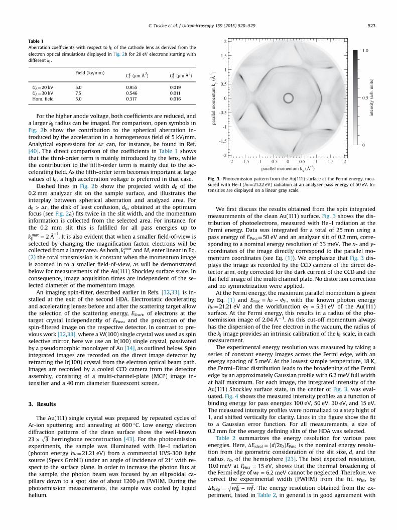
Table 1Aberration coefficients with respect to k∥ of the cathode lens as derived from the
electron optical simulations displayed in Fig. 2b for 20 eV electrons starting withdifferent k∥ .
Field (kv/mm)C ( m A )S
k 3μ · ˚ C ( m A )k5
5μ · ˚
UA¼20 kV 5.0 0.955 0.019UA¼30 kV 7.5 0.546 0.011Hom. field 5.0 0.317 0.016
Fig. 3. Photoemission pattern from the Au(111) surface at the Fermi energy, mea-sured with He–I (hν¼21.22 eV) radiation at an analyzer pass energy of 50 eV. In-tensities are displayed on a linear gray scale.
C. Tusche et al. / Ultramicroscopy 159 (2015) 520–529 523
For the higher anode voltage, both coefficients are reduced, anda larger k∥ radius can be imaged. For comparison, open symbols inFig. 2b show the contribution to the spherical aberration in-troduced by the acceleration in a homogeneous field of 5 kV/mm.Analytical expressions for rΔ can, for instance, be found in Ref.[40]. The direct comparison of the coefficients in Table 1 showsthat the third-order term is mainly introduced by the lens, whilethe contribution to the fifth-order term is mainly due to the ac-celerating field. As the fifth-order term becomes important at largevalues of k∥ , a high acceleration voltage is preferred in that case.
Dashed lines in Fig. 2b show the projected width d0 of the0.2 mm analyzer slit on the sample surface, and illustrates theinterplay between spherical aberration and analyzed area. Ford r0 > Δ , the disk of least confusion, dlc, obtained at the optimumfocus (see Fig. 2a) fits twice in the slit width, and the momentuminformation is collected from the selected area. For instance, forthe 0.2 mm slit this is fulfilled for all pass energies up to
k 2 Amax 1= ˚
∥−. It is also evident that when a smaller field-of-view is
selected by changing the magnification factor, electrons will becollected from a larger area. As both, k max
∥ andM, enter linear in Eq.(2) the total transmission is constant when the momentum imageis zoomed in to a smaller field-of-view, as will be demonstratedbelow for measurements of the Au(111) Shockley surface state. Inconsequence, image acquisition times are independent of the se-lected diameter of the momentum image.
An imaging spin-filter, described earlier in Refs. [32,33], is in-stalled at the exit of the second HDA. Electrostatic deceleratingand accelerating lenses before and after the scattering target allowthe selection of the scattering energy, EScatt, of electrons at thetarget crystal independently of EPass, and the projection of thespin-filtered image on the respective detector. In contrast to pre-vious work [32,33], where a W(100) single crystal was used as spinselective mirror, here we use an Ir(100) single crystal, passivatedby a pseudomorphic monolayer of Au [34], as outlined below. Spinintegrated images are recorded on the direct image detector byretracting the Ir(100) crystal from the electron optical beam path.Images are recorded by a cooled CCD camera from the detectorassembly, consisting of a multi-channel-plate (MCP) image in-tensifier and a 40 mm diameter fluorescent screen.
3. Results
The Au(111) single crystal was prepared by repeated cycles ofAr-ion sputtering and annealing at 600 °C. Low energy electrondiffraction patterns of the clean surface show the well-known23 3× herringbone reconstruction [43]. For the photoemissionexperiments, the sample was illuminated with He–I radiation(photon energy hν¼21.21 eV) from a commercial UVS-300 lightsource (Specs GmbH) under an angle of incidence of 21° with re-spect to the surface plane. In order to increase the photon flux atthe sample, the photon beam was focused by an ellipsoidal ca-pillary down to a spot size of about 1200 mμ FWHM. During thephotoemission measurements, the sample was cooled by liquidhelium.
We first discuss the results obtained from the spin integratedmeasurements of the clean Au(111) surface. Fig. 3 shows the dis-tribution of photoelectrons, measured with He–I radiation at theFermi energy. Data was integrated for a total of 25 min using apass energy of EPass¼50 eV and an analyzer slit of 0.2 mm, corre-sponding to a nominal energy resolution of 33 meV. The x- and y-coordinates of the image directly correspond to the parallel mo-mentum coordinates (see Eq. (1)). We emphasize that Fig. 3 dis-plays the image as recorded by the CCD camera of the direct de-tector arm, only corrected for the dark current of the CCD and theflat field image of the multi channel plate. No distortion correctionand no symmetrization were applied.
At the Fermi energy, the maximum parallel momentum is givenby Eq. (1) and E hmax Sν Φ= − , with the known photon energyhν¼21.21 eV and the workfunction 5.31 eVSΦ = of the Au(111)surface. At the Fermi energy, this results in a radius of the pho-toemission image of 2.04 Å�1. As this cut-off momentum alwayshas the dispersion of the free electron in the vacuum, the radius ofthe k∥ image provides an intrinsic calibration of the k∥ scale, in eachmeasurement.
The experimental energy resolution was measured by taking aseries of constant energy images across the Fermi edge, with anenergy spacing of 5 meV. At the lowest sample temperature, 18 K,the Fermi–Dirac distribution leads to the broadening of the Fermiedge by an approximately Gaussian profile with 6.2 meV full widthat half maximum. For each image, the integrated intensity of theAu(111) Shockley surface state, in the center of Fig. 3, was eval-uated. Fig. 4 shows the measured intensity profiles as a function ofbinding energy for pass energies 100 eV, 50 eV, 30 eV, and 15 eV.The measured intensity profiles were normalized to a step hight of1, and shifted vertically for clarity. Lines in the figure show the fitto a Gaussian error function. For all measurements, a size of0.2 mm for the energy defining slits of the HDA was selected.
Table 2 summarizes the energy resolution for various passenergies. Here, E d r E( /2 ) Passideal 0Δ = is the nominal energy resolu-tion from the geometric consideration of the slit size, d, and theradius, r0, of the hemisphere [23]. The best expected resolution,10.0 meV at E 15 eVPass = , shows that the thermal broadening ofthe Fermi edge of w 6.2 meVF = cannot be neglected. Therefore, wecorrect the experimental width (FWHM) from the fit, wfit, by
E w wexp fit2
F2Δ = − . The energy resolution obtained from the ex-
periment, listed in Table 2, in general is in good agreement with

Fig. 4. Measured intensity (symbols) of the Shockley surface state as a function ofbinding energy at a sample temperature of T¼18 K. Curves for EPass¼100 eV (°),EPass¼50 eV (◊), EPass¼30 eV (□), EPass¼15 eV (▵) are shifted vertically. Solid linesshow a fit by a gaussian error function (see Table 2).
Table 2Nominal ( EidealΔ ) and measured ( EexpΔ ) energy resolution for 0.2 mm analyzer slits,
obtained form the fit of a Gaussian error function to the experimental intensityprofiles in Fig. 4.
EPass EidealΔ (meV) EexpΔ (meV)
100 66.67 56.9 74.050 33.33 30.2 71.930 20.00 20.1 73.115 10.00 11.9 71.8
a
c
d
b
Fig. 5. (a) Detail of the Rashba-split Shockley surface state (E EF= ), recorded atpass energy 30 eV and using a higher momentum magnification. (b) Dispersion ofthe surface state obtained by a horizontal (ky¼0) cut through the data of(a) measured at different energies. (c) Intensity profile at ky¼0 with a fit (solid line)to a Voigt line shape with 0.005 Å�1 (FWHM) Gaussian broadening and the Lor-entzian contribution (dashed line). Numbers indicate the Lorentzian width.(d) Deviation kΔ ∥ of the radius from an ideal circular shape of the outer (solid line)and the inner (dashed line) ring.
C. Tusche et al. / Ultramicroscopy 159 (2015) 520–529524
the nominal value. For the pass energies of 30 eV and above, wefind the energy resolution equal, or slightly better than the ex-pected value. For the lowest pass energy used, 15 eV, we find
E 12 meVΔ = , i.e. 20% larger than the purely geometric expecta-tion. We assume that this additional broadening can be attributedto the stability of the energy defining voltage supplies, which wasmeasured to be better than 5 mV peak-to-peak, and residualmagnetic fields.
The Shockley surface state of Au(111) exhibits a Rashba-typesplitting into two spin sub-bands due to spin–orbit interaction[14,15]. In the two-dimensional Fermi-surface contour this man-ifests itself in two concentric circular bands with opposite spin,
which are separated by k 0.025 A1
Δ = ˚∥−. We observe this splitting
of the surface state already in the full image of the surface Bril-louin zone in Fig. 3. A better resolved quantitative measurement ofthe spectral width of the Au(111) surface state is obtained byelectron optically selecting a larger magnification of the mo-mentum image. Fig. 5a is measured with a pass energy of 30 eV,corresponding to an energy resolution of 20 meV (see Table 2). Thetwo concentric rings of the surface state are clearly separated,where the intensity in between the inner and the outer statenearly reduces to the background level.
The dispersion of the Au(111) surface state was measured byacquiring a series of momentum images at several kinetic energieswith steps of 10 meV. From this three-dimensional data set (kx, ky,E), sections along arbitrary directions can be selected. Fig. 5bshows a section along the M MΓ¯ − ¯ − ¯ direction, i.e. along thehorizontal line with ky¼0, containing a total of 63 energy slicesmeasured within 120 min. In agreement with the Rashba modelwe find the two nearly free-electron parabolas (experimentallydetermined effective mass m m/ 0.250e
* = ). A quantitative analysisof the measured peak positions and line shape is shown in Fig. 5c.The measured intensity profile along the horizontal line (ky¼0) atthe Fermi energy consists of four peaks, in total.
The measured intensities can be well fitted by double Voigtprofiles on the left and right side, respectively, including a linearbackground. The fitted peak positions yield a k∥ diameter of the
outer and inner ring of 70.190 �1 and 70.165 �1, respectively.The measured separation on the in-plane momentum axis thus is
k 0.025 A1
Δ = ˚∥−, in good agreement with other results [12,13]. The
instrumental momentum resolution is considerably better thanthe observed line width of the surface state and is included by acommon Gauss width parameter for all peaks. The best fit is ob-tained for an instrumental broadening of
k 0.0049 A (5)instr 1Δ = ˚∥
−
full width at half maximum (FWHM). This k∥ resolution is aboutone order of magnitude better than values obtained with a mo-mentum imaging photoelectron microscope, previously [29].
The Lorentzian line shape observed in photoemission peaks isgenerally related to the finite lifetime of the initial and final statesinvolved in the photoemission process [44,45]. The fit shown inFig. 5c (dashed line) reveals a different Lorentzian width Γ

C. Tusche et al. / Ultramicroscopy 159 (2015) 520–529 525
(FWHM) of the outer and the inner ring. We find consistently onboth sides that the outer surface state ring (Γouter¼0.0064 Å�1) is25% narrower than the inner ring (Γinner¼0.0085 Å�1). As wemeasure the width along the k axis−∥ , the more meaningful life-time energy broadening is obtained through the dispersion of therespective band (n) at the intersection with the measured energyslice
⎡⎣⎢⎢
⎤⎦⎥⎥E
Ek
Ek
kk (6)
n nn n
f
ΓΔ = ·∂∂
+∂∂
∂∂∥ ⊥
⊥
∥
As the two-dimensional surface state has no explicit dependenceon the z-momentum coordinate, the second term in Eq. (6)including the unknown final state dispersion (k f
⊥ ) vanishes [44]. Asboth parabola branches of the surface state are separated by aconstant parallel momentum, the derivative of the dispersionrelation at the Fermi energy has the same value for the innerand the outer peak and affects both line widths in the same way.From this, we obtain a value of E 34 meVouterΔ = and
E 46 meVinnerΔ = for the lifetime related energy broadening ofthe outer and the inner ring of the surface state at the Fermienergy.
The lifetime related line width measured in photoemissioncontains, in general, contributions from scattering channels due toelectron–electron, electron–phonon, and electron–defect interac-tion. The separation of the contributions usually involves as-sumptions about their functional dependence. For instance, theelectron–electron scattering related broadening for the Shockleysurface states on the noble metals was found to monotonicallyincrease with binding energy, being negligible at the Fermi level[46–48]. The spectral line width is usually studied at the Γ̄ point,neglecting a possible k∥ dependence. The latter is also not expectedin the case of the Au(111) surface, within the Rashba model [49]. Incontrast to our result, photoemission measurements in Ref. [49]did not show significantly different line widths of the inner andthe outer ring of the Au(111) surface state at the Fermi energy.However, line widths were about a factor of two larger comparedto the present results, possibly related to the surface quality of thesample or k∥ resolution.
4. Non-circularity of the surface state
Visual inspection of the Fermi surface contour in Fig. 5a showsa perfectly circular shape of the surface state. For the Shockleysurface states on the [111] fcc surfaces, the prototype of a two-dimensional nearly free electron gas, this is the expected result. Onthe close packed surfaces, the corrugation of the electron densityis smeared out and an in-plane gradient of the potential becomesnegligible. The surface state then can be effectively described by anisotropic parabolic dispersion of a free electron only characterizedby a modified effective mass m m/ 1e
* ≠ . This is not the case when aconsiderable in-plane gradient of the potential is present, for in-stance for various surface alloys like Bi/Cu(111) or Bi/Ag(111),where the six-fold rotational symmetry of the surface layer isclearly observed in the Fermi surface contour [31,50,51].
A precise measurement of the rotational symmetry of theShockley surface state by conventional ARPES by scanning thesample or analyzer is complicated by the mechanical movementinvolved. By contrast, the present momentum microscope acquiresthe complete Fermi surface contour simultaneously. Fig. 5d showsthe measured radius of the outer (solid line) and inner (dashedline) ring of the surface state, obtained from the center positions ofthe Voigt profile fit, respectively. The in-plane angle is measuredwith respect to the horizontal MΓ̄ − ¯ direction. We find a non-circularity of both surface state rings with an amplitude of
k 0.3 10 A3 1Δ ≈ · ˚∥
− −peak-to-peak, and a threefold 120° periodicity.
An estimate of the statistical uncertainty of the radius measure-ment is given by the scatter of individual data points and theagreement between the inner and the outer surface state ring.
Here, this uncertainty is of the order 0.1 10 A3 1≤ · ˚− −
peak-to-peak,and clearly distinguished from the observed three-foldmodulation.
Instrumental distortions can be excluded as the source of thethree-fold radial symmetry for several reasons: first, the electronoptical system does not contain elements with a three-fold sym-metry. The major breaking of the rotational symmetry is in-troduced by the energy filter, which however might give rise to atwo-fold astigmatism along the ky axis. Such contributions can beclearly separated from the observed three-fold periodicity. Moreimportantly, we additionally checked that the three-fold periodi-city of the surface state radius is aligned with the crystal axes ofthe sample. For this, the Au(111) sample was mechanical rotated,while all other parameters of the instrument were left unchanged.We found that this rotation leads to a corresponding phase shift in
k ( )ϕΔ ∥ .We conclude that the variation of the in-plane momentum
follows the three-fold bulk symmetry. A six-fold symmetry fromthe surface layer, as outlined above, is not clearly observed, butmight be present below the noise level. We therefore relate theobserved deviation from a perfect circle to the interaction betweenthe surface state and the edge of the projected bulk band gap.Previously, a deviation from the free-electron description due tohybridization with bulk states could only be observed experi-mentally when the surface state of Cu(111) approaches the edge ofthe band gap above the Fermi level [52]. A similar behavior wasalso predicted for Au(111) [21]. At the Fermi level, however, thedeviation from the free-electron gas becomes small, in general.Our results provide a quantitative estimation for limits of an iso-tropic free electron model of the Shockley surface state, for thefirst time.
5. Spin resolved results
Spin resolved photoelectron momentum distributions wererecorded by introducing a spin polarizing electron mirror into theelectron optical path after the energy filter. The principle of spinfiltering of a two-dimensional electron distribution was in-troduced earlier using a W(100) scattering target [32]. Spin con-trast is obtained due to the spin dependent reflectivity of low-energy electrons at the non-magnetic surface of the scatteringtarget which is governed by spin–orbit coupling, such that elec-trons with opposite spin see different scattering potentials, leadingto different scattering amplitudes [53]. Image information istransmitted in the momentum conserving (0 0) LEED beam. Pre-vious measurements showed that scattering energies of 26.5 eVand 30.5 eV with a spin sensitivity of 42% and 5%, respectively, areefficient working points for a clean W(100) scattering target[32,33]. Using an Ir(100) single crystal, a sharply peaked high spinasymmetry and reflectivity was found at scattering energiesaround 10 eV and a rather broad asymmetry maximum around40 eV for the clean 5�1 reconstructed surface [54]. For a pseu-domorphic monolayer of Au on Ir(100), experimental data andtheory from Ref. [34] also find an asymmetry maximum at 40 eVscattering energy under an angle of incidence of 45°, while the lowenergy region was not explored, so far. In addition, the reportedlong-term stability of the Au/Ir(100) surface of several weeksmakes this system an interesting candidate for the imaging spin-filter of the present momentum microscope.
The clean Ir(100) crystal was prepared by repetitive heating to

a
b
Fig. 6. (a) Spin averaged reflectivity (I I/ 0, left), and spin sensitivity (S, right) as afunction of the scattering energy. (b) Line profiles over the Au(111) surface state atky¼0 for E 10.25 eVScatt = (▿) and E 11.50 eVScatt = (▵) together with a model fit forS¼�0.65 and S¼þ0.57, respectively.
C. Tusche et al. / Ultramicroscopy 159 (2015) 520–529526
1400 K in an oxygen pressure of 5 10 mbar8· − followed by hightemperature heating to 1700 K under UHV conditions. The proce-dure was repeated until a carbon free surface showing the 5�1reconstruction was obtained [55]. Gold was deposited onto theclean Ir(100)-5�1 surface followed by annealing cycles of 90 sduration after which an end temperature of 1140 K was reached,until the stable unreconstructed pseudomorphic monolayer wasobtained [34].
Fig. 6a shows the reflectivity and asymmetry for scatteringenergies in the range from E 7.0 eVScatt = to E 15.0 eVScatt = , mea-sured 2 days after the Au monolayer was prepared. The scatteringenergy was varied by the potential applied to the Au/Ir(100)crystal, while the electrode voltages of the retarding and accel-erating lenses were adjusted such that the magnification of themomentum image in the 90° inclined detector arm was constant.The spin sensitivity, S, and reflectivity, R, were evaluated fromhorizontal intensity profiles taken across the Rashba split Au(111)surface state. Fig. 6b shows two intensity profiles recorded at ascattering energy of 10.25 eV and 11.50 eV. Intensities were nor-malized to the background level, for clarity. At 10.25 eV, in contrastto the spin integrated profile in Fig. 5c, only the right (↓) peak ofthe two spin sub-bands appears on both sides of the surface statering. The situation gets reversed at 11.50 eV with strong left (↑)peaks, due to reversal of S.
In order to determine the value of S from the profiles, we followa modified procedure as outlined in Ref. [56], and describe theprimary photo current, i0, and polarization, p0, by a synthesizedprofile of the partial intensities of the spin-up (i0
↑) and spin-down(i0
↓) channels
i i12
,12 (7)l r l r0 0= + + = + +↑ ↑ ↑ ↓ ↓ ↓
i i i pi i
i i,
(8)0 0 0 0
0 0
0 0= + =
−+
↑ ↓↑ ↓
↑ ↓
Here, l r,,↑ ↓ is the Voigt profile obtained from the fit in Fig. 5c for the
spin-up (↑) or -down (↓) peaks on the left (l) or right (r) side of thesurface state ring, and is the non-polarized backgroundfunction. The scattered intensities then can be written by [57]
i i p S R[ (1 ) ] , (9)s 0 0= · + · · ⁎
where S and R are scalar fit parameters for the spin-sensitivity andthe reflectivity, respectively.
The result of the fit is displayed by the dashed (10.25 eV) andsolid (11.50 eV) lines in Fig. 6b. The best fit was obtained withS¼�0.65 and R¼1.3% for 10.25 eV, and S¼þ0.57 and R¼2.3% for11.50 eV. The absolute scale of the reflectivity was calibrated bycomparing the single-electron count rates on the direct and spin-filtered detectors. Convolution by the gaussian function, , ac-counts for the reduced image resolution introduced by reflectionat the spin-filter target, where the best fit was obtained with aFWHM¼0.011 Å�1. Given the complete field-of-view of the spin-filtered image was a circle 0.90 Å�1 in diameter, this correspondsto 80 diagonal points and about N¼5000 points in the circularfield-of-view. For comparing the detection efficiency, we pre-viously introduced the two-dimensional figure-of-merit,
R S ND22= · · , where a value of 8D2 = was found for the 26.5 eV
working point of W(100) [32,33]. Using the values given above forAu/Ir(100), we find even a considerably higher efficiency of
28D2 = and 37D2 = for the two working points at ES¼10.25 eVand 11.50 eV, respectively.
Spin-resolved photoelectron momentum maps of the Au(111)surface state were measured by recording images at the workingpoints with negative and positive spin sensitivity atE 10.25 eVScatt = and E 11.50 eVScatt = . As shown in the horizontalprofiles in Fig. 6b, each of the scattering energies contains a majorcontribution from the spin-up (11.50 eV) or the spin-down(10.25 eV) spin channel. The reason for this simple interpretationis that the spin-sensitivity is almost directly opposite (�65% andþ57%) at these working points. In general, from the measurementwith two different spin sensitivities, Sl and Sh, the spin-polariza-tion P x y( , ), and analogous the spin-averaged intensity I x y( , )0 , ateach pixel, is derived according to the procedure outlined in Ref.[33]
P x yx y x y
S x y S x y( , )
( , ) ( , )( , ) ( , ) (10)
l h
l h h l=
−· − ·
I x yS x y S x y
S S( , )
( , ) ( , ),
(11)l h h l
l h0 =
−−
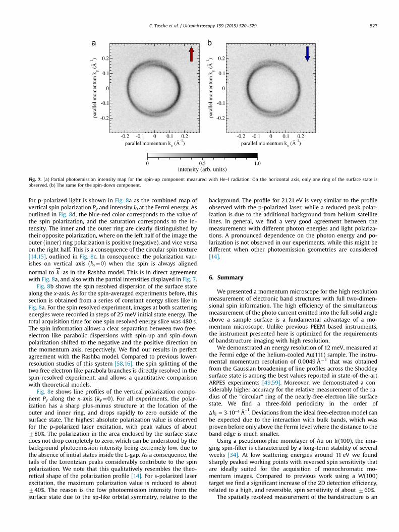
where I R/l h l h l h, , ,= is the measured intensity image I l h, normal-ized to the reflectivity reference image Rl h, for the low (l) or high(h) scattering energy [33]. As in Eq. (8) the same information alsocan be represented by the partial intensities of the spin-up (↑) andspin-down (↓) channels. Using the spin sensitivities derived above,these partial intensities for the Au(111) surface state at the Fermienergy are displayed in Fig. 7a and b. Here, maximum intensity ineach spin channel is obtained on the horizontal axis at ky¼0,where only the spin-up or spin-down component is visible in oneimage, indicating clear separation of spin channels.
While all data presented up to here was measured using un-polarized He–I radiation, for comparison we also performedmeasurements using 6.05 eV photons from the 4th harmonic of aTi:Sa oscillator ( h 10 meVνΔ ≈ , 80 MHz repetition rate). The result
a b
Fig. 7. (a) Partial photoemission intensity map for the spin-up component measured with He–I radiation. On the horizontal axis, only one ring of the surface state isobserved. (b) The same for the spin-down component.
C. Tusche et al. / Ultramicroscopy 159 (2015) 520–529 527
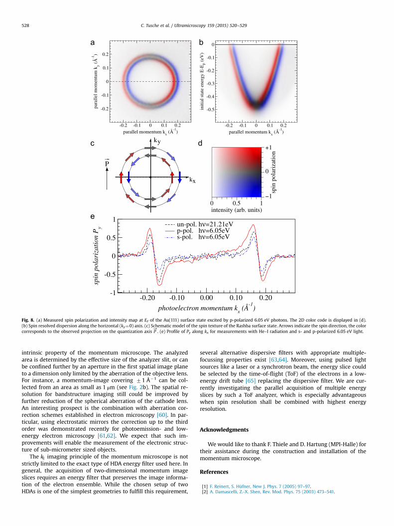
for p-polarized light is shown in Fig. 8a as the combined map ofvertical spin polarization Py and intensity I0 at the Fermi energy. Asoutlined in Fig. 8d, the blue-red color corresponds to the value ofthe spin polarization, and the saturation corresponds to the in-tensity. The inner and the outer ring are clearly distinguished bytheir opposite polarization, where on the left half of the image theouter (inner) ring polarization is positive (negative), and vice versaon the right half. This is a consequence of the circular spin texture[14,15], outlined in Fig. 8c. In consequence, the polarization van-ishes on vertical axis (kx¼0) when the spin is always aligned
normal to k→
as in the Rashba model. This is in direct agreementwith Fig. 8a, and also with the partial intensities displayed in Fig. 7.
Fig. 8b shows the spin resolved dispersion of the surface statealong the x-axis. As for the spin-averaged experiments before, thissection is obtained from a series of constant energy slices like inFig. 8a. For the spin resolved experiment, images at both scatteringenergies were recorded in steps of 25 meV initial state energy. Thetotal acquisition time for one spin resolved energy slice was 480 s.The spin information allows a clear separation between two free-electron like parabolic dispersions with spin-up and spin-downpolarization shifted to the negative and the positive direction onthe momentum axis, respectively. We find our results in perfectagreement with the Rashba model. Compared to previous lower-resolution studies of this system [58,16], the spin splitting of thetwo free electron like parabola branches is directly resolved in thespin-resolved experiment, and allows a quantitative comparisonwith theoretical models.
Fig. 8e shows line profiles of the vertical polarization compo-nent Py along the x-axis (ky¼0). For all experiments, the polar-ization has a sharp plus-minus structure at the location of theouter and inner ring, and drops rapidly to zero outside of thesurface state. The highest absolute polarization value is observedfor the p-polarized laser excitation, with peak values of about780%. The polarization in the area enclosed by the surface statedoes not drop completely to zero, which can be understood by thebackground photoemission intensity being extremely low, due tothe absence of initial states inside the L-gap. As a consequence, thetails of the Lorentzian peaks considerably contribute to the spinpolarization. We note that this qualitatively resembles the theo-retical shape of the polarization profile [14]. For s-polarized laserexcitation, the maximum polarization value is reduced to about740%. The reason is the low photoemission intensity from thesurface state due to the sp-like orbital symmetry, relative to the
background. The profile for 21.21 eV is very similar to the profileobserved with the p-polarized laser, while a reduced peak polar-ization is due to the additional background from helium satellitelines. In general, we find a very good agreement between themeasurements with different photon energies and light polariza-tions. A pronounced dependence on the photon energy and po-larization is not observed in our experiments, while this might bedifferent when other photoemission geometries are considered[14].
6. Summary
We presented a momentum microscope for the high resolutionmeasurement of electronic band structures with full two-dimen-sional spin information. The high efficiency of the simultaneousmeasurement of the photo current emitted into the full solid angleabove a sample surface is a fundamental advantage of a mo-mentum microscope. Unlike previous PEEM based instruments,the instrument presented here is optimized for the requirementsof bandstructure imaging with high resolution.
We demonstrated an energy resolution of 12 meV, measured atthe Fermi edge of the helium-cooled Au(111) sample. The instru-mental momentum resolution of 0.0049 Å�1 that was obtainedfrom the Gaussian broadening of line profiles across the Shockleysurface state is among the best values reported in state-of-the-artARPES experiments [49,59]. Moreover, we demonstrated a con-siderably higher accuracy for the relative measurement of the ra-dius of the ”circular“ ring of the nearly-free-electron like surfacestate. We find a three-fold periodicity in the order of
k 3 10 A4 1Δ = · ˚∥
− −. Deviations from the ideal free-electron model can
be expected due to the interaction with bulk bands, which wasproven before only above the Fermi level where the distance to theband edge is much smaller.
Using a pseudomorphic monolayer of Au on Ir(100), the ima-ging spin-filter is characterized by a long-term stability of severalweeks [34]. At low scattering energies around 11 eV we foundsharply peaked working points with reversed spin sensitivity thatare ideally suited for the acquisition of monochromatic mo-mentum images. Compared to previous work using a W(100)target we find a significant increase of the 2D detection efficiency,related to a high, and reversible, spin sensitivity of about 760%.
The spatially resolved measurement of the bandstructure is an
a
c
e
d
b
Fig. 8. (a) Measured spin polarization and intensity map at EF of the Au(111) surface state excited by p-polarized 6.05 eV photons. The 2D color code is displayed in (d).(b) Spin resolved dispersion along the horizontal (ky¼0) axis. (c) Schematic model of the spin texture of the Rashba surface state. Arrows indicate the spin direction, the colorcorresponds to the observed projection on the quantization axis P
→. (e) Profile of Py along kx for measurements with He–I radiation and s- and p-polarized 6.05 eV light.
C. Tusche et al. / Ultramicroscopy 159 (2015) 520–529528
intrinsic property of the momentum microscope. The analyzedarea is determined by the effective size of the analyzer slit, or canbe confined further by an aperture in the first spatial image planeto a dimension only limited by the aberration of the objective lens.For instance, a momentum-image covering 71 Å�1 can be col-lected from an area as small as 1 mμ (see Fig. 2b). The spatial re-solution for bandstructure imaging still could be improved byfurther reduction of the spherical aberration of the cathode lens.An interesting prospect is the combination with aberration cor-rection schemes established in electron microscopy [60]. In par-ticular, using electrostatic mirrors the correction up to the thirdorder was demonstrated recently for photoemission- and low-energy electron microscopy [61,62]. We expect that such im-provements will enable the measurement of the electronic struc-ture of sub-micrometer sized objects.
The k∥ imaging principle of the momentum microscope is notstrictly limited to the exact type of HDA energy filter used here. Ingeneral, the acquisition of two-dimensional momentum imageslices requires an energy filter that preserves the image informa-tion of the electron ensemble. While the chosen setup of twoHDAs is one of the simplest geometries to fulfill this requirement,
several alternative dispersive filters with appropriate multiple-focussing properties exist [63,64]. Moreover, using pulsed lightsources like a laser or a synchrotron beam, the energy slice couldbe selected by the time-of-flight (ToF) of the electrons in a low-energy drift tube [65] replacing the dispersive filter. We are cur-rently investigating the parallel acquisition of multiple energyslices by such a ToF analyzer, which is especially advantageouswhen spin resolution shall be combined with highest energyresolution.
Acknowledgments
We would like to thank F. Thiele and D. Hartung (MPI-Halle) fortheir assistance during the construction and installation of themomentum microscope.
References
[1] F. Reinert, S. Hüfner, New J. Phys. 7 (2005) 97–97.[2] A. Damascelli, Z.-X. Shen, Rev. Mod. Phys. 75 (2003) 473–541.

C. Tusche et al. / Ultramicroscopy 159 (2015) 520–529 529
[3] X. Zhou, G. Liu, J. Meng, W. Zhang, H. Liu, L. Zhao, X. Jia, Physica Status Solidi(a) (2010) 2674–2692.
[4] P. Richard, T. Sato, K. Nakayama, T. Takahashi, H. Ding, Rep. Prog. Phys. 74(2011) 124512.
[5] M. Bianchi, D. Guan, S. Bao, J. Mi, B.B. Iversen, P.D. King, P. Hofmann, NatCommun. 1 (2010) 128.
[6] D. Hsieh, Y. Xia, D. Qian, L. Wray, J.H. Dil, F. Meier, J. Osterwalder, L. Patthey, J.G. Checkelsky, N.P. Ong, A.V. Fedorov, H. Lin, A. Bansil, D. Grauer, Y.S. Hor, R.J. Cava, M.Z. Hasan, Nature 460 (2009) 1101–1105.
[7] S. Suga, K. Sakamoto, T. Okuda, K. Miyamoto, K. Kuroda, A. Sekiyama,J. Yamaguchi, H. Fujiwara, A. Irizawa, T. Ito, et al., J. Phys. Soc. Jpn. 83 (2014)014705.
[8] J. Kirschner, R. Feder, J.F. Wendelken, Phys. Rev. Lett. 47 (1981) 614–617.[9] A. Eyers, F. Schäfers, G. Schönhense, U. Heinzmann, H.P. Oepen, K. Hünlich,
J. Kirschner, G. Borstel, Phys. Rev. Lett. 52 (1984) 1559–1562.[10] R. Raue, H. Hopster, R. Clauberg, Phys. Rev. Lett. 50 (1983) 1623–1626.[11] S. LaShell, B.A. McDougall, E. Jensen, Phys. Rev. Lett. 77 (1996) 3419–3422.[12] F. Reinert, G. Nicolay, S. Schmidt, D. Ehm, S. Hüfner, Phys. Rev. B 63 (2001)
115415.[13] F. Reinert, J. Phys.: Condens. Matter 15 (2003) S693.[14] J. Henk, A. Ernst, P. Bruno, Phys. Rev. B 68 (2003) 165416.[15] J. Henk, M. Hoesch, J. Osterwalder, A. Ernst, P. Bruno, J. Phys.: Condens. Matter
16 (2004) 7581.[16] J. Osterwalder, in: Lecture Notes in Physics, vol. 697, 2006, pp. 95–120.[17] C.M. Cacho, S. Vlaic, M. Malvestuto, B. Ressel, E.A. Seddon, F. Parmigiani, Rev.
Sci. Instrum. 80 (2009) 043904.[18] C. Jozwiak, J. Graf, G. Lebedev, N. Andresen, A.K. Schmid, A.V. Fedorov, F. El
Gabaly, W. Wan, A. Lanzara, Z. Hussain, Rev. Sci. Instrum. 81 (2010) 053904.[19] C. Jozwiak, C.-H. Park, K. Gotlieb, C. Hwang, D.-H. Lee, S.G. Louie, J.D. Denlinger,
C.R. Rotundu, R.J. Birgeneau, Z. Hussain, et al., Nat. Phys. 9 (2013) 293–298.[20] Z. Xie, S. He, C. Chen, Y. Feng, H. Yi, A. Liang, L. Zhao, D. Mou, J. He, Y. Peng,
et al., Nat. Commun. 5 (2014) 3382.[21] J. Ibañez Azpiroz, A. Bergara, E.Y. Sherman, A. Eiguren, Phys. Rev. B 88 (2013)
125404.[22] S.N.P. Wissing, C. Eibl, A. Zumbülte, A.B. Schmidt, J. Braun, J. Minár, H. Ebert,
M. Donath, New J. Phys. 15 (2013) 105001.[23] F. Hadjarab, J.L. Erskine, J. Electron. Spectrosc. Relat. Phenom. 36 (1985)
227–243.[24] D. Pierce, R. Celotta, M. Kelley, J. Unguris, Nucl. Instrum. Methods Phys. Res.
Sect. A: Accel. Spectrom. Detect. Assoc. Equip. 266 (1988) 550–559.[25] A. Winkelmann, D. Hartung, H. Engelhard, C.-T. Chiang, J. Kirschner, Rev. Sci.
Instrum. 79 (2008) 083303.[26] T. Okuda, K. Miyamaoto, H. Miyahara, K. Kuroda, A. Kimura, H. Namatame,
M. Taniguchi, Rev. Sci. Instrum. 82 (2011) 103302.[27] M. Kolbe, P. Lushchyk, B. Petereit, H.J. Elmers, G. Schönhense, A. Oelsner,
C. Tusche, J. Kirschner, Phys. Rev. Lett. 107 (2011) 207601.[28] M. Kotsugi, W. Kuch, F. Offi, L.I. Chelaru, J. Kirschner, Rev. Sci. Instrum. 74
(2003) 2754–2758.[29] B. Krömker, M. Escher, D. Funnemann, D. Hartung, H. Engelhard, J. Kirschner,
Rev. Sci. Instrum. 79 (2008) 053702.[30] A. Winkelmann, C. Tusche, A.A. Ünal, M. Ellguth, J. Henk, J. Kirschner, New J.
Phys. 14 (2012) 043009.[31] A.A. Ünal, A. Winkelmann, C. Tusche, F. Bisio, M. Ellguth, C.-T. Chiang, J. Henk,
J. Kirschner, Phys. Rev. B 86 (2012) 125447.[32] C. Tusche, M. Ellguth, A.A. Ünal, C.-T. Chiang, A. Winkelmann, A. Krasyuk,
M. Hahn, G. Schönhense, J. Kirschner, Appl. Phys. Lett. 99 (2011) 032505.[33] C. Tusche, M. Ellguth, A. Krasyuk, A. Winkelmann, D. Kutnyakhov, P. Lushchyk,
K. Medjanik, G. Schönhense, J. Kirschner, Ultramicroscopy 130 (2013) 70–76.[34] J. Kirschner, F. Giebels, H. Gollisch, R. Feder, Phys. Rev. B 88 (2013) 125419.[35] M.J. Pellin, C.E. Young, D.M. Gruen, Scanning Microsc. 2 (1988) 1353.[36] M. Escher, N. Weber, M. Merkel, C. Ziethen, P. Bernhard, G. Schönhense,
S. Schmidt, F. Forster, F. Reinert, B. Krömker, D. Funnemann, J. Phys.: Condens.Matter 17 (2005) S1329–S1338.
[37] D. Funnemann, M. Escher, Patent EP 1 559 126 B1.[38] D.A. Dahl, Int. J. Mass Spectrom. 200 (2000) 3–25.[39] M. Bernheim, Eur. Phys. J. Appl. Phys. 36 (2006) 193–204.[40] E. Bauer, Ultramicroscopy 17 (1985) 51–56.[41] P.W. Hawkes, J. Phys. D: Appl. Phys. 1 (1968) 131.[42] R. Tromp, Ultramicroscopy 111 (2011) 273–281.[43] M. Van Hove, R. Koestner, P. Stair, J. Bibrian, L. Kesmodel, I. Barto, G. Somorjai,
Surf. Sci. 103 (1981) 189–217.[44] N.V. Smith, P. Thiry, Y. Petroff, Phys. Rev. B 47 (1993) 15476–15481.[45] J. Sánchez-Royo, J. Avila, V. Pérez-Dieste, M. Asensio, Surf. Sci. 482–485 (2001)
752–758.[46] T. Valla, A.V. Fedorov, P.D. Johnson, S.L. Hulbert, Phys. Rev. Lett. 83 (1999)
2085–2088.[47] J. Kliewer, R. Berndt, E.V. Chulkov, V.M. Silkin, P.M. Echenique, S. Crampin,
Science 288 (2000) 1399–1402.[48] A. Eiguren, B. Hellsing, F. Reinert, G. Nicolay, E.V. Chulkov, V.M. Silkin,
S. Hüfner, P.M. Echenique, Phys. Rev. Lett. 88 (2002) 066805.[49] I.A. Nechaev, M.F. Jensen, E.D.L. Rienks, V.M. Silkin, P.M. Echenique, E.
V. Chulkov, P. Hofmann, Phys. Rev. B 80 (2009) 113402.[50] J. Premper, M. Trautmann, J. Henk, P. Bruno, Phys. Rev. B 76 (2007) 073310.[51] C.R. Ast, J. Henk, A. Ernst, L. Moreschini, M.C. Falub, D. Pacilé, P. Bruno, K. Kern,
M. Grioni, Phys. Rev. Lett. 98 (2007) 186807.[52] A.A. Ünal, C. Tusche, S. Ouazi, S. Wedekind, C.-T. Chiang, A. Winkelmann,
D. Sander, J. Henk, J. Kirschner, Phys. Rev. B 84 (2011) 073107.[53] J. Kirschner, R. Feder, Phys. Rev. Lett. 42 (1979) 1008–1011.[54] D. Kutnyakhov, P. Lushchyk, A. Fognini, D. Perriard, M. Kolbe, K. Medjanik,
E. Fedchenko, S. Nepijko, H. Elmers, G. Salvatella, C. Stieger, R. Gort, T. Bähler,T. Michlmayer, Y. Acremann, A. Vaterlaus, F. Giebels, H. Gollisch, R. Feder,C. Tusche, A. Krasyuk, J. Kirschner, G. Schönhense, Ultramicroscopy 130 (2013)63–69.
[55] K. Heinz, G. Schmidt, L. Hammer, K. Müller, Phys. Rev. B 32 (1985) 6214–6221.[56] F. Meier, J.H. Dil, J. Osterwalder, New J. Phys. 11 (2009) 125008.[57] J. Kessler, chapter 3, in: Polarized Electrons, 2 edition, Springer-Verlag, Berlin,
Heidelberg, New York, Tokyo, 1985, ISBN: 0-387-15736-0.[58] M. Hoesch, M. Muntwiler, V.N. Petrov, M. Hengsberger, L. Patthey, M. Shi,
M. Falub, T. Greber, J. Osterwalder, Phys. Rev. B 69 (2004) 241401.[59] A. Nuber, J. Braun, F. Forster, J. Minár, F. Reinert, H. Ebert, Phys. Rev. B 83 (2011)
165401.[60] M. Haider, S. Uhlemann, E. Schwan, H. Rose, B. Kabius, K. Urban, Nature 392
(1998) 768–769.[61] T. Schmidt, A. Sala, H. Marchetto, E. Umbach, H.-J. Freund, Ultramicroscopy 126
(2013) 23–32.[62] R. Tromp, J. Hannon, W. Wan, A. Berghaus, O. Schaff, Ultramicroscopy 127
(2013) 25–39.[63] W. Poschenrieder, Int. J. Mass Spectrom. Ion Phys. 6 (1971) 413–426.[64] M. Ishihara, M. Toyoda, T. Matsuo, Int. J. Mass Spectrom. 197 (2000) 179–189.[65] G. Schönhense, A. Oelsner, O. Schmidt, G. Fecher, V. Mergel, O. Jagutzki,
H. Schmidt-Böcking, Surf. Sci. 480 (2001) 180–187.