spin-dependent transport in nanoscale structures - Cornell University
125
SPIN-DEPENDENT TRANSPORT IN NANOSCALE STRUCTURES A Dissertation Presented to the Faculty of the Graduate School of Cornell University in Partial Fulfillment of the Requirements for the Degree of Doctor of Philosophy by Kirill I. Bolotin January 2007
Transcript of spin-dependent transport in nanoscale structures - Cornell University

SPIN-DEPENDENT TRANSPORT IN NANOSCALE
STRUCTURES
A Dissertation
Presented to the Faculty of the Graduate School
of Cornell University
in Partial Fulfillment of the Requirements for the Degree of
Doctor of Philosophy
by
Kirill I. Bolotin
January 2007

This document is in the public domain.

SPIN-DEPENDENT TRANSPORT IN NANOSCALE STRUCTURES
Kirill I. Bolotin, Ph.D.
Cornell University 2007
If a metallic particle is sufficiently small (< 15 nm), its discrete spectrum of “elec-
tron in a box” states can be resolved by tunnel spectroscopy at low temperatures.
We will first discuss a technique that introduces several previously unavailable
“knobs” to study the quantum states of an individual nanoparticle: we can control
the number of electrons on the particle by using efficient gate electrodes, and the
size and composition of the particle using chemical synthesis. In gold nanoparti-
cles we find that quantum states are spin-degenerate and are filled as in a non-
interacting model, consistent with weak exchange interactions. The second part of
the thesis focuses on developing ferromagnetic contacts to study spin-dependent
transport through the nanoparticle. We discuss a technique which allows us to
fabricate such contacts with tunable size down to the atomic scale and into the
tunneling regime, and to study spin transport in atomically-narrow contacts. We
find a large anistropic magnetoresistance contribution in such contacts and inter-
pret it as a consequence of mesoscopic quantum interference.

BIOGRAPHICAL SKETCH
Kirill Igorevich Bolotin was born in Moscow, Russia in 1978. After attending sev-
eral schools further and further away from his home, he finally found the fartherst
one (School N1543, one-hour long subway ride away). After almost failing the
chemistry class, he somehow graduated in 1994. He then joined the physics pro-
gram in Moscow Institute of Physics and Techology. After several years in college
he found an adviser working on quantum gravity and decided only to study sys-
tems larger than galaxies. In the year 2000, he introduced several small corrections
to this course: he decided to switch from theory to experiments, length scale from
large to small, and the country from Russia to America and joined Dan Ralph’s
group at Cornell. Six years down the road, Kirill is happily mixing chemicals in
the lab and takes prides in his soldering. His next stop is Columbia University,
where he will work in the Philip Kim and Horst Stormer groups.
iii

ACKNOWLEDGEMENTS
I would like to thank all the friends and colleagues who made these six years in
Ithaca enjoyable and productive.
I am most grateful to my advisor, Dan Ralph, for all the support and patience
over the years. Dan, from my day one when you taught me soldering the right
wayTM you were the best boss one can ask for. Thanks to you, I had all the helium
and equipment I could ask for, all the freedom to explore the ideas I liked and all
the advice when I needed it. I now understand how one can preserve his scientific
integrity, follow what is important not what is fashionable, stay humble, and yet
remain on top of his field.
Experiments are a team effort, and I was lucky to be a member of the best
team in town. Ralph group, you were my family for the last six years, and I would
like to thank both elder and younger brothers and sisters.
Mandar and Ed, thanks for sharing your wisdom and showing me the ropes
around the lab. Thanks to you, the lab became a great and fun place it is now.
Jason, thanks for setting the example to the expression “to work hard”. You have
it all - lots of ideas, tremendous talent, and passion for work; I hope to see you a
full professor before I finish my postdoc.
Abhay, you were my hero from the day I joined the group, your intelligence
and creativity sometimes seemed almost intimidating; much of what I know about
experiments I have learned from you. Thanks for both teaching me how to get
and stay cold and for letting me into your project. I have no doubt about a great
academic future in front of you, I have but one request - stay in the US for your
professorship.
iv

Alex, thanks for being a good friend. Your wisdom and intelligence helped me
many times over the years. If now I can hard-solder and tell the difference between
a hefeweizen and a blonde beer it is thanks to you.
On all of the projects I worked on, I collaborated with Ferdinand. I have yet
to meet a better experimentalist or a better labmate - smart, passionate, hard-
working. You taught me countless lessons about experiments and became my very
good friend - I am very grateful for that. It was very hard not to get jealous on your
excellence in whatever you were taking on be it nanofabrication or windsurfing.
Just stay confident and only the sky will be your limit.
If it were not for Jack, I would not know much about programming. Thank
you for that, and for being a good friend all these years. Remember, it just takes
one hour to commute from Princeton to Manhattan, so I expect to see you often.
Jacob, it is in part due to you that I evolved from almost failing chemistry to
starting my own nanoparticle synthesis. Thanks for that.
Thank you Josh for all the discussions ranging in topics from Kondo to Borat
and for being a good friend.
Kiran, thanks for feeding me Indian food from time to time, I wish you the
best of luck with the 3D magnet. Sufei, you are rapidly becoming a skilled exper-
imentalist. Thanks for putting up with me for the last couple of months and good
luck.
I was blessed to collaborate with a stellar undergraduate. Thiti, thank you and
best of luck with your paper. I have learned a lot from group’s postdocs - Sergey,
Edgar, Ilya, Janice, you were an invaluable source of wisdom and advice. I would
like to thank my special committee members - Paul McEeuen and Piet Brouwer.
Your help and encouragement were a blessing.
v
McEuen and Buhrman groups - thanks for making Clark Hall basement a won-
derful place it is. Thank you Scott, Vera, Marcus, Arend, Yuval, Sami, Shahal,
Xinjian, Luke, Greg, Pat, Eric, Preeti, Nate, EiLeen, Phil.
A very special thank you for Eric Smith - his willingness to help is only sur-
passed by the depth of his physics knowledge. All I know about machining is due
to Sned. Thank you for teaching me about Zen and the art of machining.
Life would have been sad without my friends in Ithaca. Saikat, Ben, Ribhu,
Jahan, Faisal, Amar, Sharvari, Peter, Danya, Sahak, Ivan, Senya - thank you, guys.
Camille, thank you were for putting up with me for all these years, you made my
life much more enjoyable.
Finally, thanks to my parents for everything they have done for me. Mom and
Dad, you are the best.
vi
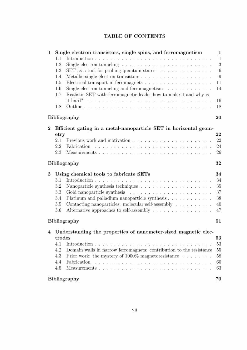
TABLE OF CONTENTS
1 Single electron transistors, single spins, and ferromagnetism 11.1 Introduction . . . . . . . . . . . . . . . . . . . . . . . . . . . . . . . 11.2 Single electron tunneling . . . . . . . . . . . . . . . . . . . . . . . . 31.3 SET as a tool for probing quantum states . . . . . . . . . . . . . . 61.4 Metallic single electron transistors . . . . . . . . . . . . . . . . . . . 91.5 Electrical transport in ferromagnets . . . . . . . . . . . . . . . . . . 111.6 Single electron tunneling and ferromagnetism . . . . . . . . . . . . 141.7 Realistic SET with ferromagnetic leads: how to make it and why is
it hard? . . . . . . . . . . . . . . . . . . . . . . . . . . . . . . . . . 161.8 Outline . . . . . . . . . . . . . . . . . . . . . . . . . . . . . . . . . . 18
Bibliography 20
2 Efficient gating in a metal-nanoparticle SET in horizontal geom-etry 222.1 Previous work and motivation . . . . . . . . . . . . . . . . . . . . . 222.2 Fabrication . . . . . . . . . . . . . . . . . . . . . . . . . . . . . . . 242.3 Measurements . . . . . . . . . . . . . . . . . . . . . . . . . . . . . . 26
Bibliography 32
3 Using chemical tools to fabricate SETs 343.1 Introduction . . . . . . . . . . . . . . . . . . . . . . . . . . . . . . . 343.2 Nanoparticle synthesis techniques . . . . . . . . . . . . . . . . . . . 353.3 Gold nanoparticle synthesis . . . . . . . . . . . . . . . . . . . . . . 373.4 Platinum and palladium nanoparticle synthesis . . . . . . . . . . . . 383.5 Contacting nanoparticles: molecular self-assembly . . . . . . . . . . 403.6 Alternative approaches to self-assembly . . . . . . . . . . . . . . . . 47
Bibliography 51
4 Understanding the properties of nanometer-sized magnetic elec-trodes 534.1 Introduction . . . . . . . . . . . . . . . . . . . . . . . . . . . . . . . 534.2 Domain walls in narrow ferromagnets: contribution to the resistance 554.3 Prior work: the mystery of 1000% magnetoresistance . . . . . . . . 584.4 Fabrication . . . . . . . . . . . . . . . . . . . . . . . . . . . . . . . 604.5 Measurements . . . . . . . . . . . . . . . . . . . . . . . . . . . . . . 63
Bibliography 70
vii

5 Anisotropic magnetoresistance due to quantum interference inferromagnets 725.1 Introduction . . . . . . . . . . . . . . . . . . . . . . . . . . . . . . . 725.2 Brief overview: Mesoscopic conductance fluctuation due to quantum
interference . . . . . . . . . . . . . . . . . . . . . . . . . . . . . . . 735.3 Quantum interference in ferromagnets . . . . . . . . . . . . . . . . . 765.4 AMR due to quantum interference: the experiment . . . . . . . . . 775.5 Looking back: domain walls & quantum inteference . . . . . . . . . 87
Bibliography 93
6 Conclusions and possible experiments 956.1 Progress towards ferromagnetic SETs . . . . . . . . . . . . . . . . . 966.2 Electromigration after depositing the nanoparticles . . . . . . . . . 1016.3 Nanoparticle deposition inside the refrigerator . . . . . . . . . . . . 1036.4 SETs with ferromagnetic electrodes: theoretical proposals . . . . . . 1046.5 More proposals for future experiments . . . . . . . . . . . . . . . . 108
Bibliography 111
viii

LIST OF FIGURES
1.1 a) A diagram of a single-electron transistor (SET). (b) The currentas a function of the voltage bias across the SET is suppressed at lowbias voltage. (c) Coulomb blockade region in the V −VG plane; thenumber of electrons N and N + 1 on the SET’s island is constantin time inside each region. The capacitance CL, CR, CG can beextracted from the slopes −CG
CL+ 12
and CG
CR+ 12
of the sides of the region
(C = CL + CR + CG) and the spacing e/VG between neighboringdegeneracy points. . . . . . . . . . . . . . . . . . . . . . . . . . . . 4
1.2 (a) Current as a function of bias across the SET. Steps in currentare observed as individual states become available for tunneling.(b), (c), (d), (e) Different stages of electronic transport through anSET. (f) SET’s conductance as a function of V and VG. Particle-in-a-box states show up as lines in the V − VG plane. . . . . . . . . 7
1.3 Band structure of a typical metallic ferromagnet. The DOS for thed band is spin split by the exchange interaction. . . . . . . . . . . . 11
1.4 (a) Tunneling between two ferromagnetic electrodes. The anglebetween magnetization ML of the left and of the right MR electrodesis θ. (b) A single-electron transistor with ferromagnetic leads. Non-trivial spin S can be accumulated on the island. . . . . . . . . . . . 14
2.1 A cartoon of the device of Ralph et al. [9]. A nanometer-sized holeis used to make stable electrical contacts to a nanoparticle . . . . . 23
2.2 (a) Top-view scanning electron microscope (SEM) image of the de-vice geometry, with gold source and drain electrodes on top of anoxidized aluminum gate. (b) Expanded view of the region outlinedwith a white rectangle in (a). A 10-nm gap made by electromigra-tion is visible, along with deposited gold nanoparticles. (c) Circuitschematic for the Au-nanoparticle SET. . . . . . . . . . . . . . . . 25
2.3 . (a) Coulomb staircase I − V curve for a gold nanoparticle SET(device #1) at 4.2 K, along with an orthodox model fit (offset forclarity). (b) I−V curves for device #1 at 4.2 K, for equally spacedvalues of VG. (c) Gray-scale plot of dI/dV as a function of VG and Vfor device #1 at 4.2 K. Eleven degeneracy points separating twelvedifferent charge states are visible within a 2 V range of VG. (d)Gray-scale plot of dI/dV as a function of VG and V for device #2at 4.2 K, showing ”Coulomb diamonds” as well as several abruptchanges in the background charge of the SET island as VG is swept. 27
ix

2.4 Gray-scale plots of dI/dV as a function of VG and V , displaying thediscrete electron-in-a-box level spectra within a gold nanoparticle(device #3), measured with an electron temperature less than 150mK and zero magnetic field. Panels (a), (b), and (c) representspectra for different numbers of electrons in the same nanoparticle.Panel (b) covers the gate voltage range from -95 mV to -110 mVand (c) the range from -180 mV to -195 mV. Insets: Energy-leveldiagrams illustrating the tunneling transitions that contribute toline for different numbers of electrons on the particle. . . . . . . . . 29
3.1 Gold nanoparticles (Ted Pella) of different sizes. The particles arehighly spherical and monodisperse. . . . . . . . . . . . . . . . . . . 38
3.2 Palladium nanoparticles synthesized using the method of Choo etal. [16] . . . . . . . . . . . . . . . . . . . . . . . . . . . . . . . . . 39
3.3 Platinum nanoparticles synthesized using the modified the methodof Sarathy et al. [17]. . . . . . . . . . . . . . . . . . . . . . . . . . 40
3.4 Using chemical self-assembly to place the nanoparticle onto theelectrodes. A molecule with two functional endgroups may be usedto attach the nanoparticle to the substrate. . . . . . . . . . . . . . 41
3.5 The acidity of the gold nanoparticle solution can be adjusted tocontrol the surface coverage of the nanoparticles. . . . . . . . . . . 43
3.6 Gold nanoparticle between two electodes resulting in a stable singleelectron transistor . . . . . . . . . . . . . . . . . . . . . . . . . . . 44
3.7 Conductance (colorscale) as a function of bias and gate voltages fora chemically synthesized metallic nanoparticle SET. The island ofthe SET is a 15 nm gold nanoparticle (Ted Pella), APTS moleculesbind the particle to the electrodes. . . . . . . . . . . . . . . . . . . 46
3.8 Gold nanoparticles are only deposited onto the electrode kept atthe positive bias (on the left). . . . . . . . . . . . . . . . . . . . . . 47
3.9 Gold nanoparticles are placed between the electrodes using electro-static trapping. . . . . . . . . . . . . . . . . . . . . . . . . . . . . . 50
4.1 Domain wall contributing to ferromagnet’s resistance due to AMR. 564.2 (a) Scanning electron micrograph of a finished device. Gold elec-
trodes are used to contact two permalloy thin-film magnets (inset)on top of an oxidized aluminum gate. The irregular shape of thePy electrodes results from imperfect liftoff during fabrication. (b)Micromagnetic modeling showing antiparallel magnetic alignmentacross the tunneling gap in an applied magnetic field of H= 66 mT. 61
x

4.3 The cross section of a constriction is reduced in stages (a,b,c) byrepeatedly ramping the bias voltage until electromigration begins,and then quickly decreasing the bias, following a procedure similarto that in [18]. The SEM micrographs illustrate the gradual nar-rowing of the constriction, which appears bright in these images.Inset: Resistance as a function of magnetic field for a tunneling de-vice exhibiting abrupt switching between parallel and antiparallelmagnetic states. . . . . . . . . . . . . . . . . . . . . . . . . . . . . 62
4.4 (a) Magnetoresistance as a function of resistance in the range lessthan 400 Ω (device I). (b) Magnetoresistance as a function of re-sistance in the range 60 Ω - 15 kΩ (device II). Inset: Switchingbehavior of device II at different resistances (curves are offset ver-tically for clarity.) . . . . . . . . . . . . . . . . . . . . . . . . . . . 64
4.5 The evolution of magnetoresistance in the tunneling regime (deviceIII) as the resistance of the tunneling gap is changed by electromi-gration (curves are vertically offset for clarity). Inset: distributionof magnetoresistances for devices in the tunneling regime (> 20 kΩ). 66
4.6 Differential conductance as a function of bias voltage for device IVat small (a), intermediate (b) and large (c) resistances. (d) Mag-netoresistance as a function of bias for a tunneling device (deviceV). . . . . . . . . . . . . . . . . . . . . . . . . . . . . . . . . . . . . 68
5.1 Cartoon diagram representing an electron’s trajectory in diffusivemetals when τe ¿ τφ. Circle represent elastic scattering from theimpurities, squares represent inelastic scattering from phonons . . . 74
5.2 (a) Zero-bias differential resistance vs. angle of applied magneticfield at different field magnitudes at 4.2 K, illustrating bulk AMRfor a constriction size of 30 × 100 nm2 and resistance R0 = 70 Ω(device A). (b) SEM micrograph of a typical device. . . . . . . . . 78
5.3 (a) Evolution of AMR in device B as its resistance R0 is increasedfrom 56 Ω to 1129 Ω. (b) AMR for a R0 = 6 kΩ device (device C)exhibiting 15% AMR, and a R0 = 4 MΩ tunneling device (deviceD), exhibiting 25% TAMR. All measurements were made at a fieldmagnitude of 800 mT at 4.2 K. Inset: AMR magnitude as a functionof R0 for 12 devices studied into the tunneling regime. . . . . . . . 79
5.4 Variations of R = dV/dI at 4.2 K in a sample with average zero-bias R0 = 2.6 kΩ (device E). (a) R vs. field angle at different biasvoltages (|B| = 800 mT). (b) Dependence of R on V at differentfixed angles of magnetic field (|B| = 800 mT). The curves in (a)and (b) are offset vertically. (c) R as a function of V and magneticfield strength, with field directed along the x axis. R does not havesignificant dependence on the magnitude of B. (d) R as a functionof V and θ, for |B| = 800 mT. . . . . . . . . . . . . . . . . . . . . 81
xi

5.5 Variations of R = dV/dI at 4.2 K in a sample with average zero-biasR0 = 257 kΩ (device F), in the tunneling regime. (a) R vs. fieldangle at different bias voltages (|B| = 800 mT). (b) Dependence ofR on V at different fixed angles of magnetic field (|B| = 800 mT).The curves in (a) and (b) are offset vertically. (c) R(V ) − Rav(V )as a function of V and magnetic field strength, with field directedalong the x axis. Rav(V ), the average of R(V ) over angle (shownin (b)), is subtracted to isolate angular-dependent variations. (d)R(V ) − Rav(V ) as a function of bias voltage and magnetic fieldangle, for |B| = 800 mT. . . . . . . . . . . . . . . . . . . . . . . . 83
5.6 Domain wall contribution to the magnetoresistance for a 60 Ωpermalloy device. (a) Change in resistance as a function of mag-netic field angle. (b) Change in resistance as a function of magneticfield strength; the field is applied along the x axis (blue curve) andy axis (pink curve) . . . . . . . . . . . . . . . . . . . . . . . . . . . 89
5.7 Domain wall contribution to magnetoresistance for a 7 kΩ permal-loy device. (a) Change in resistance as a function of magnetic fieldangle. (b) Change in resistance as a function of magnetic fieldstrength; the field is applied along the x axis (blue curve) and yaxis (pink curve) . . . . . . . . . . . . . . . . . . . . . . . . . . . . 90
5.8 Domain wall contribution to mesoscopic interference for 19 kΩpermalloy device. (a) R(V) as a function of bias voltage and mag-netic field angle, for ‖B‖ = 800 mT (b) R(V) as a function ofmagnetic field strength, with magnetic field directed along the xaxis. Note the switching events near zero field. (c) R(V) as a func-tion of bias voltage for ‖B‖ = 6 mT and ‖B‖ = 8 mT. Note thechange in resistance. . . . . . . . . . . . . . . . . . . . . . . . . . . 92
6.1 Conductance (colorscale) as a function of gate and bias voltage foran SET with gold island and nickel electrodes. . . . . . . . . . . . 97
6.2 Conductance (colorscale) as a function of magnetic field and biasvoltage for a metallic SET with gold island and ferromagnetic(nickel) leads. Note the shift of particle-in-a-box states around+40 mT . . . . . . . . . . . . . . . . . . . . . . . . . . . . . . . . 97
6.3 Conductance (colorscale) as a function of the applied magnetic fieldfrom -8 T to +8 T and bias voltage for an SET with gold islandand nickel electrodes. Note the asymmetry in the electron levelswith respect to zero field. . . . . . . . . . . . . . . . . . . . . . . . 98
6.4 The conductance of a ferromagnetic tunneling gap protected byaluminum and silicone oxide capping layers monitored after elec-tromigration. The conductance slowly decreases as the chamber isvented with dry nitrogen and drops to zero as the chamber is openedto air, suggesting that ferromagnetic electrodes may be oxidized. . 100
xii

6.5 (a) Electromigration of gold electrodes after a self-assembled mono-layer of gold nanoparticles was deposited. Notice the absence of thenanoparticles next to the gap between the electrodes. (b) Same as(a), except that before electromigration the SAM of nanoparticleswas treated with ethanol solution of hexenedithiol. Note the parti-cles in the gap region. . . . . . . . . . . . . . . . . . . . . . . . . . 102
6.6 (a) A filament is extracted from a conventional lightbulb. (b) Thefilament is placed next to the chip on a helium dipstick. . . . . . . 103
6.7 (a) After passing a current through the filament the metal depositedon the filament gets redeposited onto the surface of the chip (b)Some of the tunneling devices change their resistance and exhibita Coulomb blockade after the evaporation. . . . . . . . . . . . . . . 105
6.8 The results of Martinek et al. [7]. (Reproduced with permissionfrom Jan Martinek.) (a), (b) Current across a ferromagnetic SET asa function of bias voltage in the non-linear regime, for different po-larizations p of the electrons at the Fermi level. (a) Magnetizationin the left and right electrode directed in the opposite directions(θ = 180). (b) θ = 90. (c) Differential conductance of the SET inthe linear response regime eV < kT as a function of angle betweenthe magnetization direction of the two electrodes θ, for differentgate voltages ε. . . . . . . . . . . . . . . . . . . . . . . . . . . . . . 106
6.9 The results of Martinek et al. [16]. (Reproduced with permissionfrom Jan Martinek). Differential conductance across the SET inthe linear response regime as a function of applied magnetic field,with magnetization of the leads aligned antiparallel. The widthat half-maximum of the resonance is inversely proportional to thespin-relaxation time. . . . . . . . . . . . . . . . . . . . . . . . . . . 108
xiii

Chapter 1
Single electron transistors, single spins,
and ferromagnetism
1.1 Introduction
Bohr is right after all.
W. Gerlach
In 1922, Otto Stern and Walther Gerlach directed a beam of silver atoms passing
through a gradient of magnetic field onto a glass plate. The resulting thin film of
metal was almost invisible, but when the smoke from Stern’s cheap cigar turned
silver into silver sulfide, two black lines clearly appeared on the plate [1]. The
two lines signified two electron spin-states, marking the first observation of space
quantization.
Much has changed over the last 80 years, and we do not have to rely on cigar
smoke anymore: Thanks to MRI imaging, looking at collective spin properties has
become a part of the everyday duties of a medical doctor in a big hospital. However,
the interest in all things spin-related is on a big rise among physicists: the number
of papers containing the word “spin” in the title, for example, increased more
than tenfold between the years 1960 and 2005 [2]. This interest is at least in part
due to the progress towards electrical creation and manipulation of spin-polarized
electron currents. Suddenly, the electronic analog of optical experiments with
polarized light became possible, with ferromagnets in place of optical polarizers
and normal metals in place of optical fibers.
Such experiments are not solely motivated by sheer curiosity: employing the
1

2
electron’s spin degree of freedom holds a great promise for the next generation
of electronic devices. The emerging “spintronics” technology may offer higher
degrees of integration, nonvolatility, and lower power consumption compared to
traditional semiconducting technology [3, 4, 5]. Of course, our ability to manipulate
the spin degree of freedom is far behind our ability to manipulate conventional
electrical currents. We do not yet know, for example, how to obtain 100% polarized
spin currents. Nevertheless, we can try looking into the future and consider the
possibilities down the road assuming that spintronics follows the same avenue as
electronics did. Nowadays semiconducting technology allows studying routinely
tunneling of individual electrons [7], resolving single electronic quantum states
[6], and even entangling the wavefunctions of two electrons [8]. We can imagine
experiments with similar level of control for spins: Is it possible to detect a spin of
a single electron? Can we create and measure a spin eigenstate? How robust can
we make this eigenstate?
Broadly defined, this thesis tries to tackle some of these questions. Of course,
the problems outlined above are very general (and hard, needless to say), so we
focus on one particular example of a device which is capable of measuring spin
eigenstates: the single electron transistor (or SET) with ferromagnetic electrodes.
The work in this thesis has been started with the idea in mind to develop the basic
building blocks for such an SET, and while we are at it, to explore the underlying
physics. Over the years, some of the seemingly simple problems of understanding
particular SET components became research topics of their own, and hence now
this thesis includes topics ranging from mesoscopic interference in ferromagnets to
chemical self-assembly of nanoparticle monolayers.
In this introductory chapter we briefly discuss the basics of single-electron tun-

3
neling and ferromagnetism refering the reader to in-depth reviews and previous the-
ses whenever possible. We also review both experimental and theoretical progress
towards spin manipulation in single electron transistors.
1.2 Single electron tunneling
The single-electron transistor (SET) is the most basic device probing the quanti-
zation of the electron’s charge. A schematic of an SET is shown in Figure 1.1(a);
its main components are the source electrode, the drain electrode, the gate elec-
tode, and the island which is separated from the rest of the electrodes by tunnel
barriers. The device is a mesoscopic descendant of a conventional MOSFET and
hence allows modulating the current flowing between the source and the drain
electrodes by changing the gate voltage. Let us consider the SET in Figure 1.1(a),
with capacitances of the island to the gate, right and left electrodes CG, CR, CL
respectively; the voltage applied to the gate, right and left electrode being VG, VR,
VL. The potential energy E(N) of the island with N electrons is given by [20]
E(N) =e2
2C(N − nD)2 − e2
2Cn2
D, (1.1)
nD = (CLVL + CRVR + CGVG)/e (1.2)
where C = CL + CR + CG. The main energy scale of the Eq. (1.1) is set by the
Coulomb energy Ec = e2/2C; it can be understood as work required to add one
electron to an isolated particle with the self-capacitance C. While negligible for a
conventional transistor, for a very small device the Coulomb energy may become a
dominant energy scale. For example, for a 15 nm metallic sphere we can estimate
Ec ∼ 100 meV.
For an SET at low temperature kT ¿ Ec, energy conservation requires that

4
VL
VG
IslandTunnel barriers
(a)
Bias voltage
Cur
rent
Coulomb blockade
(b)
VR
eN e(N+1)
e/CG VGV
-CG/(CL+½)
(c)
CG/(CR+½)
Figure 1.1: a) A diagram of a single-electron transistor (SET). (b) The current as
a function of the voltage bias across the SET is suppressed at low bias voltage.
(c) Coulomb blockade region in the V − VG plane; the number of electrons N and
N + 1 on the SET’s island is constant in time inside each region. The capacitance
CL, CR, CG can be extracted from the slopes −CG
CL+ 12
and CG
CR+ 12
of the sides of the
region (C = CL +CR +CG) and the spacing e/VG between neighboring degeneracy
points.

5
an electron from the left (right) lead may tunnel onto the island with the initial
charge eN when
E(N + 1)− E(N) ≤ eVL(R). (1.3)
Similarly, an electron may leave the island with charge e(N +1) to tunnel into the
left(right) lead when
E(N + 1)− E(N) ≥ eVL(R). (1.4)
The conditions (1.4) and (1.3) indicate that electrons tunnel from and onto the
island as to minimize its potential energy E(N); the equation (1.1) indicates that
the equilibrium electron number N is simply given by the integer closest to nD. We
also note that nD explicitly depends on the gate voltage Vg, providing a convenient
“knob” to adjust the equilibrium number of electrons on the island.
When N is at minimum both conditions Eq. (1.3) and Eq. (1.4) are violated for
small bias voltage and tunneling is suppressed (Coulomb blockade). The case of
half-integer nD = N + 12
is exceptional: tunneling is possible at zero bias because
E(N + 1) − E(N) = 0 (Eq. (1.1)), and the SET is said to be at its degeneracy
point. As a result the current across the SET at small bias V < kT exhibits
“Coulomb oscillations” as a function of gate voltage with period ∆VG determined
by the condition
∆VG = e/CG. (1.5)
When the bias voltage |VL(R)| exceeds E(N+1)−E(N) the Coulomb blockade is
lifted, as the battery can provide enough energy to change the number of electrons
on the island by one, but not more. Thus, current can start to flow by shuttling
one electron first onto the island across the left tunnel barrier and then off the
island across the right tunnel barrier (Fig. 1.1(b)).

6
In our experiments we typically measure the conductance of the SET as a
function of both gate VG and bias V = VL = −VR voltage (symmetric biasing)
in order to extract the effective capacitances CL,CR, and CG of Figure 1.1(a).
In V − VG plane, the region of Coulomb blockade is diamond-shaped, with the
constraints Eq. (1.3) and Eq. (1.4) determining the slopes of the diamond’s sides;
Figure 1.1(c) illustrates the process of determining the capacitances from the shape
of the Coulomb diamonds.
1.3 SET as a tool for probing quantum states
Quantum-mechanical confinement leads to another qualitative change as an SET’s
size gets smaller. This occurs when the particle-in-a-box level spacing of the island
becomes comparable to the temperature. In that case the density of states of the
island can no longer be considered continuous; individual particle-in-a-box states
spaced an average ∆ apart contribute to transport. Experimentally, fine features
due to tunneling through individual particle-in-a-box states appear on top of the
non-linear conductance due to the Coulomb blockade (Fig. 1.2(a)).
Let us consider how this happens: Let’s assume that at zero bias voltage the
energy of the N electron ground states eN is equal to the energy of the N+1 electron
ground state eN + 1. In this case electrons are shuttled through the SET by first
tunneling from the left lead into the island thus bringing it to the N+1 electron
ground state (Fig. 1.2(b)) and then from the island into the left lead, leaving the
island in the N electron ground state (Fig. 1.2(c)).
Let us now imagine that the bias voltage is increased and an electron from
the right lead can tunnel into either of the two single-electron levels (Fig. 1.2(d));
the tunneling rate in this situation is given by the sum of the tunneling rates for

7
V
Coulomb blockade,
N+1 electrons
Coulomb blockade,N electrons
VG
(c)Excited N+1 electron states
Exc
ited
N
elec
tron
sta
tes
Degeneracy point E(N)=E(N+1)
Figure 1.2: (a) Current as a function of bias across the SET. Steps in current
are observed as individual states become available for tunneling. (b), (c), (d), (e)
Different stages of electronic transport through an SET. (f) SET’s conductance as
a function of V and VG. Particle-in-a-box states show up as lines in the V − VG
plane.

8
both states. Then the electron from either state can tunnel out into the right lead
(Fig. 1.2(e)), once again at the increased rate. Hence, as a new state becomes
available for tunneling, the tunneling rates (and the current) increase. We can
thus see than the current across the SET increases in steps (Fig. 1.2(a)), with
each step corresponding to the Fermi level of one of the electrodes aligned with a
single-electron level inside the particle.
Quantitatively, when individual single-electron levels are taken into account
equation (1.1) gives the energy of the island with N electrons in the ground state.
We can express the energy of the excited state |α〉 by adding the term εα(N) > 0
to Eq. (1.1). In that case, state |α〉 contributes to tunneling of electrons to (from)
the particle when the modified Eqs. (1.3) and Eq. (1.4) hold true
E(N + 1)− E(N) + εα(N + 1) ≤ eVL(R), (1.6)
E(N + 1)− E(N)− εα(N) ≥ eVL(R). (1.7)
These equations define a set of lines in the V −VG plane (Fig. 1.2(f)); SET conduc-
tance measurement as a function of bias and gate voltage allows visual extraction
of both occupied and unoccupied single-electron levels. In order to determine the
energies of the particle-in-a-box states the capacitance ratios determined as in
Fig. 1.1(c) should be taken into account.
Three conditions should be fulfilled for to resolve single-electon energy levels
[20]:
• The temperature kT must be smaller than the level spacing ∆
• The tunneling rates Γ of the states should be small enough so that the tunnel-
induced level width hΓ does not cause the neighboring levels to overlap.

9
• For the same reason, the inelastic relaxation rate for the excited states Γinel
should be small enough so that the corresponding linewidth hΓinel is smaller
the the level spacing ∆.
If all of the above conditions are met we can extract a wealth of information
about the quantum-particle-in-a-box states of the SET by means of conductance
measurements. In addition to the positions of both occupied and unoccupied
electronic states we can estimate the tunnel couplings of individual state to the
electrodes and in some cases the lifetimes of the excited states [11].
1.4 Metallic single electron transistors
As we have seen, SETs can be used as a tool for studying quantum states in confin-
ing potentials. Very basic quantum mechanical problems can therefore be studied,
ranging from the influence of the confining potential’s shape on the distribution
of the quantum states to the interplay of superconductivity and quantum confine-
ment. Several experimental approaches to fabricate SETs are available depending
on the problem one wants to study. We briefly mention three very different fab-
rication strategies: 2-DEG SETs (or quantum dots), carbon nanotube SETs, and
metal nanoparticle SETs.
Single electron transistors are routinely fabricated by employing electrostatic
gates defined on top of a two-dimensional electron gas (2-DEG) in GaAs/AlGaAs
heterostructures [27]. A negative voltage applied to the gates results in pinching
off a “puddle” from the electron sea, forming a single electron transistor. The
geometry of the SET may be adjusted by changing the gate voltages to fine-tune
the Coulomb energy, level spacing and tunnel couplings. However, the physics
that can be accessed using such SETs is limited by the materials compatible with

10
semiconducting technology. In particular, it is very hard or impossible to fabricate
2-DEGs manifesting many-body effects such as superconductivity or magnetism.
Due to its one-dimensional nature, a carbon nanotube is an excellent choice
for the island of an SET. Nanotubes are typically contacted using top evaporated
metallic electrodes on top of a silicon or metal gate; both single-electron charg-
ing and transport through individual electronic states have been demonstrated in
carbon-nanotube SETs [9]. Due to its low atomic weight (and small spin-orbit
interaction) carbon is considered a promising material for spintronics applications,
and controllable spin-injection into nanotubes has recently attracted a lot of inter-
est [14].
In this thesis we focus on the third approach, using a mesoscopic metallic grain
connected to metallic electrodes as the SET. The main advantage of the approach
is the extent of the physics which can be accessed: the metal of either island
or electrodes can be chosen ferromagnetic, antiferromagnetic or superconducting
allowing the study of different aspects of correlated electron physics. Of course,
there is a price to pay for this versatility: The electron density of a typical metal is
very large compared to semiconductors and in order to resolve individual particle-
in-a-box states, the island of a metallic SET needs to be nanometer-sized. Let us
look at some numbers: The energy level spacing ∆ of a metallic particle can be
estimated in free-electron model as [20]
∆ =2π2h2
mkF V, (1.8)
where kF is the Fermi wavevector, V is particle’s volume, and m is electron’s
effective mass. In order to observe quantum confinement effects and to study the
transport through particle-in-a-box states in a metallic nanoparticle, the energy
level spacing ∆ needs to be larger than the temperature kT . For T ∼100 mK

11yyyyyyyyyyyyyyys
d EF d
k
E
Figure 1.3: Band structure of a typical metallic ferromagnet. The DOS for the d
band is spin split by the exchange interaction.
(typical electron temperature in a dilution refrigerator base temperature) and a
typical metal with kF ∼ 10 nm−1 this sets an upper limit of 20 nm on the size of
the island of the SET.
Clearly, such an SET cannot be fabricated using conventional electron beam
lithography (EBL): the island of the SET should be aligned with respect to the
electrodes with near-nanometer accuracy, more than by a factor of 20 smaller than
what EBL allows; this alone makes fabricating such an SET a complicated task.
1.5 Electrical transport in ferromagnets
Conductance measurements similar to the ones discussed above may be used to
probe precession, relaxation, and decoherence of single spins in SETs with ferro-
magnetic leads. Electrical transport in a ferromagnet however is sensitively coupled
to its magnetization direction (magnetoresistive effects), complicating interpreta-
tion of conductance measurements. Thus, before discussing ferromagnetic SETs,
in this section we briefly review the basics of magnetotransport in ferromagnets.
The band structure of a ferromagnet is markedly different from that of a normal
metal. A typical metallic ferromagnet (Ni, Co, Fe) has partially filled 4s and 3d

12
electron bands. The density of states of the d band is spin-split by the exchange
interaction; the majority spin states (along magnetization direction) are shifted
with respect to the minority spin states (antiparallel to the magnetization), as
shown in Figure 1.3. As a result, the DOS at the Fermi level differs between
majority and minority electrons, as quantified by the polarization ratio
p =ν↑ − ν↓ν↑ + ν↓
, (1.9)
where ν↓ and ν↑ is the density of states for minority and majority electrons at the
Fermi level. Nickel, for example, has a polarization ratio of ∼ 20%.
While the distinction between the delocalized s states and more localized d
states is important (for instance, the anisotropy in magnetoresistance is caused by
s− d scattering), phenomenological models of electrical transport in ferromagnets
neglect the difference between s and d electrons. The transport is then described
in terms of the so-called “two current model”, treating the currents of spin-up and
spin-down electrons independently.
There are several magnetoresistive (MR) effects that couple the magnetization
of ferromagnets to their transport properties. We briefly mention two of them,
anisotropic magnetoresistance (AMR) and tunneling magnetoresistance (TMR).
Anisotropic magnetoresistance is the dependence of a ferromagnet’s resistance
∆R on the angle φ between the magnetization direction and the direction of cur-
rent:
∆R ∼ cos2(φ)− 1/2 (1.10)
AMR is caused by the anisotropy in electron scattering due to spin orbit interaction
and is typically a small effect in most materials (∆R/R < 1%). Much of the
research into AMR effect is motivated by the interest from magnetic recording
industry; until recently the AMR effect was used in every hard-drive read-head.

13
Tunneling magnetoresistance is observed for a system of two ferromagnetic elec-
trodes separated by a tunneling gap (a spin valve); in such a system the tunneling
current acquires a dependence on the angle between the magnetization vectors of
the two electrodes (Fig. 1.4(a)). TMR can be easily (albeit not very accurately)
explained using Fermi golden rule considerations. Following Julliere [23], we can
estimate the tunneling current IP for the parallel alignment of the leads using the
two current model and assuming spin conservation during tunneling
IP ∝ ν↑Lν↑R + ν↓Lν↓R, (1.11)
where νσr is the spin-resolved DOS at the Fermi level in either left (r = L) or right
(r = R) lead. Similarly, for an antiparallel configuration of the leads we obtain
IAP ∝ ν↑Lν↓R + ν↓Lν↑R, (1.12)
For the case of the same material right and left electrodes (νLσ = νRσ) we get
IAP < IP or, in other words, the resistance of a spin-valve in minimal when the
magnetization of the electrodes is aligned. Quantitatively, the TMR can be de-
scribed by the magnetoresistance ratio
TMR =IP − IAP
IAP
=2pLpR
1− pLpR
(1.13)
Typical values for the magnetoresistance of ferromagnet-metallic oxide-ferromagnet
structures are in the range of tens of percent, however recently the TMR ratios
in excess of 100% were reported at room temperature (e.g. [25] and references
therein).
The equation (1.13) may be generalized for an arbitrary angle θ between ML
and MR [24]:
I(θ)− IAP
IAP
=2pLpR
1− pLpR
cos2(θ
2) (1.14)

14
ML MR
(a) e
ML MR
(b)e e
VG
VbiasIS
θ
Figure 1.4: (a) Tunneling between two ferromagnetic electrodes. The angle be-
tween magnetization ML of the left and of the right MR electrodes is θ. (b) A
single-electron transistor with ferromagnetic leads. Non-trivial spin S can be ac-
cumulated on the island.
Although this expression has a similar functional form to that of AMR (1.10) the
size of the TMR effect is much larger; the mechanism of TMR has to do with
electron tunneling compared to the spin-dependent scattering in case of AMR.
1.6 Single electron tunneling and ferromagnetism
Embedding a metallic grain between two ferromagnetic electrodes significantly
changes the simple picture of spin-polarized tunneling. Several factors contribute
to the complexity of the resulting single-electron transistor with spin polarized
leads (Fig. 1.4(b)) compared to its normal-metal counterpart:
• Depending on the polarization of the electrodes, the left and right tunnel

15
barriers may preferentially transmit the electrons of different spin. In that
case, at finite bias voltage a non-trivial spin can be accumulated on the
dot. The accumulated spin depends on the angle θ between magnetization
direction of the two leads.
• The accumulated spin precesses in an applied magnetic field, making a simple
description of the SET in terms of rate equations for two spin components
impossible.
• The tunneling of the electrons between the island and the leads may be
described in terms of an effective magnetic field; the electron precesses in
this field even in the absence of the external field.
• Accumulated spin modifies the DC conductance across the SET.
SETs with spin-polarized leads were demonstrated in several recent experiments:
• In the approach of Ono et al. [13] a lithographically-fabricated aluminum
island was contacted using ferromagnetic electrodes, allowing the observation
of single-electron charging.
• Sahoo et al. [14] succeded in contacting an individual nanotube using PdNi
alloy electrodes and studied gate-voltage dependent magnetoresistance in
such a spin valve.
• Pasupathy et al. [21] fabricated a single molecule SET in the regime of
strong coupling to the leads to study the coexistance of Kondo effect and
ferromagnetism.
• Davidovic et al. [22] studied conductance through a network of metallic

16
clusters sandwiched between two ferromagnetic electrodes and observed sig-
natures of the Hanle effect.
Despite the number of publications, the field of single-spin manipulation is in its
infancy; there is a lot of room for new, better controlled experiments. Leaving more
detailed discussion of the underlying physics for later, we mention the theoretical
prediction of Braig et al. [10] concerning the case of a quantum dot with several
quantum levels and highly spin-polarized electrodes. Braig et al. showed that the
step heights of Figure 1.2(a) change between parallel and antiparallel orientation of
the electrodes’ magnetization. This distinct experimental signature indicates both
the spin-accumulation on the SET’s island and the interplay of spin-accumulation
and electronic transport.
1.7 Realistic SET with ferromagnetic leads: how to make
it and why is it hard?
As we have seen, an SET with ferromagnetic leads provides an exciting playground
for the manipulation of single spins. Let us now consider closely how different
components of the idealized device (Figure 1.4(b)) may be achieved experimentally
and what kind of problems we are likely to encounter.
Electrodes with high degree of spin polarization First, we need ferromag-
netic leads with high degree of polarization p of the electrons at the Fermi
level. Polarization ratios for metallic ferromagnets are not very high: e.g.
∼ 30% for iron, ∼ 20% for cobalt [28]. Magnetic semiconductors can be
engineered to reach higher p, but making a reliable contact to such semicon-
ductors, however, is a formidable and currently unsolved task.

17
Ferromagnetic materials are notoriously tricky to engineer at the nanoscale.
First, metallic ferromagnets (Ni, Co, Fe) oxidize in ambient atmosphere, re-
sulting in deteriorated magnetic properties. Second, ferromagnets tend to
change their shape as magnetic field is applied and special care needs to be
taken to avoid artifacts related to this mechanical motion. Finally, while
little experimental work has been done on near-atomically-narrow ferromag-
nets, the theory hints that their magnetic and transport properties may be
dominated by quantum effects.
Nanoscopic SET island As discussed earlier, the requirement of resolving quan-
tum states in a nanoparticle puts an upper limit on the size of SET’s island
to about twenty nanometers, ruling out e-beam lithography as the primary
fabrication tool. For the same reason, shadow-evaporation-like techniques
[18] are also out of the question. Most of the alternative pathways to the
problem rely on self-assembly as part of the fabrication and all share a very
low yield of working devices [17].
Material of the SET island Spin-orbit (SO) interaction can significantly per-
turb the electronic eigenstates of the nanoparticle by mixing spin-up and
spin-down states [12]. We can avoid this mixing by choosing the material
of the SET island to have a low atomic number Z, as the strength of SO
interaction scales as Z4. Aluminum, with a Z of 13 has been a metal of
choice for spintronics experiments; all-aluminum SETs have been fabricated
in the past [19]. However, aluminum readily oxidizes in air and special care
should be taken to avoid unwanted oxidation.
Well-coupled gate electrode For the tunneling current to flow through just one

18
quantum state, the SET needs to operate near its degeneracy point, where
the energies of two states differing by one electron are equal. The relative
energies of the two states can be adjusted using the gate electrode. An
efficient gate electrode can also serve as a knob for tuning the number of
electrons on the island; this control is important for some of the experiments
described in this thesis. For efficient gating, the gate electrode needs to be
as close to the island as possible. Ideally, the gate is separated from the
island only by a thin (∼ 3 nm) layer of gate oxide. The challenge here is to
fabricate highly uniform pinhole-free oxide compatible with the rest of the
fabrication.
Controlled tunnel barriers The choice of the optimal tunnel coupling between
the island of the SET and the electrodes is a result of a trade-off: In order to
observe the unperturbed particle-in-a-box states we would like the coupling
to be as small as possible. Experimentally, however, the largest resistance
we can measure reliably is of the order of tens of gigaohms, which sets the
lower limit on the tunnel coupling. Thus, it is advantageous to control the
tunnel barriers separating the island of the SET from the electrodes. Metallic
oxides have been used in the past to form controlled tunnel barriers in SETs.
In our setup, however, we would like to avoid oxidization of ferromagnetic
electrodes, which makes the use of oxide tunnel barriers problematic.
1.8 Outline
This thesis is largely focused on realizing the components needed for ferromagnetic
SETs and understanding the underlying physics; each chapter is roughly focused

19
on a different component of the device.
In the second chapter, we discuss our strategy for realizing an efficient gate
electrode. We fabricate our model normal-metal SET in a horizontal geometry
in order to test the gate action. We are able to tune the charge of the island by
more than 30 electrons and observe the evolution of quantum states as electrons
are added to the island one-by-one.
In the third chapter we describe progress towards controlling the island and
the tunnel barriers of the SET using chemical self-assembly. We fabricate SETs
using chemically synthesized nanoparticles of well-controlled size and composition
and thiolated molecules serving as tunnel barriers.
The design, fabrication and understanding the properties of nanoscale magnetic
electrodes is the focus of the fourth chapter. We use controlled electromigration to
fabricate ferromagnetic breakjunctions with large predictable TMR. We then use
the same setup to study the scattering of electrons by atomically sharp magnetic
domain walls.
In the fifth chapter we discuss physics of magnetotransport in nanoscale ferro-
magnetic junctions. Angle resolved measurements of magnetotransport reveal that
quantum interference plays an important role in electronic transport in atomic-
sized ferromagnetic contacts. We observe mesoscopic conductance fluctuations in
ferromagnetic point contacts and examine their contribution to the increased AMR
of the devices.
Finally, in the last (sixth) chapter, we review the work done in this thesis and
discuss the possibilities for new experiments.

20
BIBLIOGRAPHY
[1] O. Stern, in Les Prix Nobel en 1946, Imprimerie Royale Norstedt and Soner,Stockholm (1948), p. 123.
[2] According to the Web of ScienceTM . The increase is not caused by a meredifference in the number of papers: the number of papers containing genericterms in the title (such as “resonance”) did not change significantly betweenthe same years.
[3] S. A. Wolf, D. D. Awschalom, R. A. Buhrman, J. M. Daughton, S. von Molnar,M. L. Roukes, A. Y. Chtchelkanova, and D. M. Treger, Science 294, 1488(2001).
[4] G. Prinz, Science 282, 1660 (1998).
[5] I. Zutic, J. Fabian, and S. Das Sarma, Rev. Mod. Phys. 76, 323 (2004).
[6] D. R. Stewart, D. Sprinzak, C. M. Marcus, C. I. Duruoz, and J. S. Harris, Jr.,Science 278, 1784 (1997).
[7] L. M. K. Vandersypen, J. M. Elzerman, R. N. Schouten, L. H. Willems vanBeveren, R. Hanson, and L. P. Kouwenhoven, Appl. Phys. Lett. 85, 4394(2004).
[8] A. C. Johnson, J. R. Petta, J. M. Taylor, A. Yacoby, M. D. Lukin, C. M.Marcus, M. P. Hanson, and A. C. Gossard, Nature 435, 925 (2005).
[9] M. Bockrath, D. H. Cobden, P. L. McEuen, N. G. Chopra, A. Zettl, A. Thess,and R. E. Smalley, Science 275, 1922 (1997).
[10] S. Braig and P. W. Brouwer, Phys. Rev. B 71, 195324 (2005).
[11] M. Deshmukh, Ph. D. Thesis (2002).
[12] J. Petta, Ph. D. Thesis (2003).
[13] K. Ono, H. Shimada, and Y. Ootuka, J. Phys. Soc. Jpn. 66, 1261 (1997).
[14] S. Sahoo, T. Kontos, J. Furer, C. Hoffmann, M. Graber, A. Cottet, and C.Schonenberger, Nature Physics 1, 99 (2005).
[15] X. Waintal and P. W. Brouwer, Phys. Rev. Lett. 91, 247201 (2003).
[16] J. Martinek, Jozef Barnas, S. Maekawa, H. Schoeller, and G. Schon, Phys.Rev. B 66, 014402 (2002).
[17] D. L. Klein, R. Roth, A. K.L.Lim, A. Paul Alivisatos, and Paul L. McEuen,Nature 389 , 699 (1997).

21
[18] T. A. Fulton and G. J. Dolan, Phys. Rev. Lett. 59, 109 (1987).
[19] D. C. Ralph, C. T. Black, and M. Tinkham, Phys. Rev. Lett. 78, 4087 (1997).
[20] J. von Delft and D. C. Ralph Phys. Rep 345, 61 (2001).
[21] A. N. Pasupathy, R. C. Bialczak, J. Martinek, J. E. Grose, L. A. K. Donev,P. L. McEuen, and D. C. Ralph, Science 306, 86 (2004).
[22] L. Y. Zhang, C. Y. Wang, Y. G. Wei, X. Y. Liu, and D. Davidovic, Phys. Rev.B 72, 155445 (2005).
[23] M. Julliere, Phys. Lett A 54, 225 (1975).
[24] J. C. Slonczewski, Phys. Rev. B 39, 6995 (1989).
[25] S. S. P. Parkin, C. Kaiser, A. Panchula, P. M. Rice, B. Huges, M. Samant,and S-H Yang, Nature Mat. 3, 862 (2004).
[26] S. I. Kiselev, J. C. Sankey, I. N. Krivorotov, N. C. Emley, R. J. Schoelkopf,R. A. Buhrman, and D. C. Ralph, Nature 425, 380 (2003).
[27] S. Datta, Electronic transport in mesoscopic systems, Cambridge Universitypress (1995).
[28] R. O’Handley, Modern magnetic materials, Wiley (2000).

Chapter 2
Efficient gating in a metal-nanoparticle
SET in horizontal geometry
2.1 Previous work and motivation
Still round the corner there may wait,
A new road or a secret gate.
J. R. R. Tolkien
Our first goal is to establish electrical contacts to a metallic grain small enough
to exhibit electron level quantization due to confinement at dilution refrigerator
temperatures. As outlined in the introductory chapter, this means that the con-
tacts should be aligned with respect to the grain with a near-nanometer accuracy,
ruling out conventional lithographic techniques as a primary fabrication method.
In addition, in order to study the transport through individual electron states, an
efficient gate electrode is required. Several groups have tried to push the resolution
limits of e-beam lithography (EBL) to study such ultra-small SETs. Pashkin et
al. [10] used shadow evaporation in combination with EBL to fabricate an SET
with an island smaller than 10 nm. The gate capacitance, however, was so small
(< 10−20 F) in the approach of Pashkin et al. that the charge of the island could
not be adjusted by more than one electron.
Electron level quantization in a nanometer-sized metallic grain has been re-
liably demonstrated by Dan Ralph and co-workers [8]. Stable electrical contact
to a grain was achieved by first “drilling ” a hole in a suspended silicon nitride
membrane using reactive ion etching and a top metallic electrode was deposited by
22

23
Figure 2.1: A cartoon of the device of Ralph et al. [9]. A nanometer-sized hole is
used to make stable electrical contacts to a nanoparticle
thermal evaporation of aluminum (Fig. 2.1). A submonolayer of metal was then
evaporated from the other side, and nanometer-sized particles self-assembled under
the influence of surface tension. The tunnel barriers were formed by letting oxygen
into the chamber and letting the oxidation form tunnel barriers on both side of
the device. The device fabrication was finalized by depositing a bottom aluminum
electrode (Fig. 2.1). This fabrication method was proven to be versatile; the in-
terplay of superconductivity and quantum confinement, nanoscale ferromagnetism
and the spin-orbit interaction were studied using this geometry. However, in order
to produce the ultimate SET design for studying particle-in-a-box states in metals
we would like to improve on several shortcomings of the design of Fig. 2.1:
• Efficient gate electrode adjusting the charge of the island is very hard to
implement; the yield of devices with good gate action is prohibitively low.
• Direct imaging of the device is not possible.
• The particle size, shape and composition are poorly controlled.
In this chapter we describe our progress towards resolving the first two of the
shortcomings. We fabricate metal-nanoparticle SETs in a horizontal geometry

24
with gate capacitances of order 10−18 F, sufficient to tune the number of electrons
in a nanoparticle by more than ten. We use these devices to study the evolution of
the electron-in-a-box level spectrum in gold nanoparticles as the electron number
is changed one by one.
In the next chapter we focus on the last listed shortcoming, and use chemical
self-assembly to both fabricate the island of the SET and control the tunnel barriers
separating the island from the electrodes.
2.2 Fabrication
Our fabrication technique builds upon work in which electrical contact was made
to single nanoparticles without a gate electrode [10, 11, 12, 13] and to networks
of particles in the presence of a gate [14]. We start by using photolithography to
define a 16-nm-thick Al gate electrode with 2 nm of Ti as a sticking layer, on top
of an oxidized Si substrate. The gate electrode is deposited with the substrate at
liquid nitrogen temperature. The Al is warmed overnight to room temperature
while in 50 mtorr of oxygen and then exposed to air [15]. Next we use electron-
beam lithography and liftoff to fabricate Au wires with a thickness of 16 nm and
a minimum width of 100 nm on top of the gate (Fig. 2.2a). After cleaning the
Au wires in oxygen plasma, we submerge the chip in liquid helium and break the
wires using electromigration [16]; a source-drain bias is slowly ramped up until the
wire breaks and the conductance drops suddenly [17]. In most cases this happens
at a bias of ∼ 1 V, and results in a gap about 5-10 nm wide after the sample is
warmed to room temperature (Fig. 2.2b). A similar process of electromigration
has been used recently to make single-molecule transistors [18, 19]. Then we create
nanoparticles, formed by self-assembly, by evaporating Au on top of the broken

25
Figure 2.2: (a) Top-view scanning electron microscope (SEM) image of the device
geometry, with gold source and drain electrodes on top of an oxidized aluminum
gate. (b) Expanded view of the region outlined with a white rectangle in (a). A
10-nm gap made by electromigration is visible, along with deposited gold nanopar-
ticles. (c) Circuit schematic for the Au-nanoparticle SET.
lines and into the gap with the substrate at room temperature. For most samples
we evaporate 20 A of gold at 0.6 A/s, which produces particle diameters of 5-
15 nm as measured via SEM (Fig. 2.2b). When measured immediately after the
evaporation, approximately 25% of the junctions show a drop of resistance into the
MΩ range, indicating that a nanoparticle may be bridging the gap. This procedure
has the virtue of producing nanoparticles separated from the gate electrode by only
2-3 nm of aluminum oxide, giving excellent coupling between the particle and the
gate. Finally the devices are protected by evaporating 100 nm of aluminum oxide
prior to air exposure.

26
2.3 Measurements
We cool the finished devices to 4.2 K and measure their current-voltage (I − V )
curves as a function of gate voltage (VG) (see Fig. 2.2c for circuit conventions).
More than 50% of the devices that show a decrease in resistance during the
nanoparticle deposition step exhibit Coulomb-blockade characteristics (Fig. 2.3a
and 2.3b). Fits to the orthodox theory of Coulomb blockade [20] yield good agree-
ment (Fig. 2.3a). The variation of dI/dV as a function of VG and V is shown in
Fig. 2.3c, for a range of VG large enough to span several ”Coulomb diamonds”. The
presence of only one positive and one negative slope for the tunneling thresholds
vs. VG indicates that transport is indeed occurring through a single nanoparticle
[21]. The gate capacitance CG is determined from the spacing in VG between the
degeneracy points where dI/dV is nonzero at V = 0. For device #1 (Fig. 2.3a-c),
the spacing between neighboring degeneracy points is 180 mV, so CG = e/(180
mV) = 0.89 aF (±5 %). This is an order of magnitude greater than gate capaci-
tances achieved previously in metal nanoparticle transistors [9]. The ratios CD/CG
and CS/CG for the drain and source capacitances are then determined from the
slopes of the tunneling thresholds vs. VG [22], yielding for device #1 CD = 2.4 aF
and CS = 1.3 aF (±10 %). Fig. 2.3c demonstrates that 12 different charge states
within this nanoparticle can be accessed by varying VG within the range ±1 V.
We should note that the scan in Fig. 2.3c is somewhat atypical in that there are
very few discontinuities in the gate-voltage dependence, corresponding to sudden
rearrangements in the background charge near the particle. The diamond plot in
Fig. 2.3d, from device #2, is more typical.
The yield given by our fabrication process is that 15-20% of all devices exhibit
gate-dependent Coulomb blockade. The gate capacitances are typically 0.3-2.0 aF

27
Figure 2.3: . (a) Coulomb staircase I − V curve for a gold nanoparticle SET
(device #1) at 4.2 K, along with an orthodox model fit (offset for clarity). (b)
I − V curves for device #1 at 4.2 K, for equally spaced values of VG. (c) Gray-
scale plot of dI/dV as a function of VG and V for device #1 at 4.2 K. Eleven
degeneracy points separating twelve different charge states are visible within a 2 V
range of VG. (d) Gray-scale plot of dI/dV as a function of VG and V for device
#2 at 4.2 K, showing ”Coulomb diamonds” as well as several abrupt changes in
the background charge of the SET island as VG is swept.

28
and the source and drain capacitances are 1-10 times larger, yielding charging ener-
gies between 15 and 50 meV. As a control experiment, we took 24 devices through
the full fabrication process except for the step in which the nanoparticles are de-
posited. These samples never showed Coulomb-blockade characteristics. In prior
work, tunnel junctions containing individual metal nanoparticles have been used
to measure the “electron-in-a-box” states inside the nanoparticle, and these exper-
iments have been a rich source of information about electronic interactions within
metals [8, 9]. Having a more effective gate can contribute greatly to these types
of studies, by enabling investigations of how the spectra change as electrons are
added to a nanoparticle, and also by giving increased control over non-equilibrium
excitations [22]. Next we demonstrate that our SETs are sufficiently stable to al-
low measurements of the electron-in-a-box spectra, and we present initial studies
of how these spectra depend on the electron number.
In order to resolve electron-in-a-box quantum states, we cool samples in a
dilution refrigerator with filtered electrical lines so that the electron temperature
is less than 150 mK. In Fig. 2.4 we examine a device with parameters CG = 2.0 aF,
CS = 1.9 aF and CD = 2.2 aF. Low-temperature plots of dI/dV versus VG and V
reveal a fine structure of lines beyond the tunneling threshold that correspond to
tunneling via excited quantum states within the nanoparticle. Figure 2.4 shows
three sets of spectra. In panel (a), the lines running parallel to the line labeled
α correspond to transitions in which an electron tunnels off the nanoparticle to
decrease the total number of electrons from some value N to N − 1. Panel (b)
displays a more negative range of VG where transitions from N−1 electrons to N−2
are visible. Finally, the levels in panel (c) correspond to N−2 to N−3 transitions.
The most striking aspect of these three plots is that the pattern of excited states

29
Figure 2.4: Gray-scale plots of dI/dV as a function of VG and V , displaying the
discrete electron-in-a-box level spectra within a gold nanoparticle (device #3),
measured with an electron temperature less than 150 mK and zero magnetic field.
Panels (a), (b), and (c) represent spectra for different numbers of electrons in the
same nanoparticle. Panel (b) covers the gate voltage range from -95 mV to -110
mV and (c) the range from -180 mV to -195 mV. Insets: Energy-level diagrams
illustrating the tunneling transitions that contribute to line for different numbers
of electrons on the particle.

30
is extremely similar. The only significant difference can be seen in the line labeled
α at the threshold for tunneling. In panel (a) line α is strong, in panel (b) it is
present but its conductance is decreased by approximately 45%, and in (c) the
line is absent. This behavior can be understood in a simple way by assuming that
the energy levels in the nanoparticle are spin-degenerate, and that N corresponds
to an even number of electrons. In this case, line α in panel (a) corresponds to
transitions in which either one of the two (spin-degenerate) electrons in the highest
occupied energy level for N electrons tunnels off of the particle into the source.
For N − 1 electrons in panel (b), one of these two electrons is already gone, so line
α corresponds to having just the one remaining electron in that same energy level
tunnel off of the particle. Because the source-particle interface is the rate limiting
barrier in this device, the tunneling rate is reduced by approximately a factor of 2.
Finally, in panel (c), no electrons are left to tunnel out of the state corresponding
to line α, so the line is no longer present.
The strong similarities that we observe in the excited state spectra for different
numbers of electrons on a gold nanoparticle are in striking contrast to analogous
studies of GaAs quantum dots [23]. In GaAs dots, spin degeneracy is not gen-
erally observed and excited-state levels are shifted relative to one another when
the electron number is changed. These spectral rearrangements in GaAs have
been explained as due to exchange interactions between the added electron and
quantum-dot states with different total spins. The similarity of the excited-state
spectra that we observe for different numbers of electrons in gold is therefore ev-
idence that exchange interactions are sufficiently weak that the energy levels are
filled as in a non-interacting model, with each energy level spin-degenerate and
with the energy-level spacings not sensitive to the electron number. This simple

31
outcome is highly non-trivial for an interacting-electron system, but it is consistent
with expectations for the low strength of exchange interactions in gold [24].
In summary, we have fabricated single-electron transistors by depositing metal
nanoparticles within break junctions made using electromigration. This method
provides strong coupling between the nanoparticle and the gate electrode, thereby
enabling experiments in which the number of electrons on the particle is varied
over a wide range. We have demonstrated that this device geometry permits
detailed measurements of electron-in-a-box level spectra in metals as a function of
the electron number.

32
BIBLIOGRAPHY
[1] D. V. Averin and K. K. Likharev, J. Low Temp. Phys. 62, 345 (1986).
[2] T. A. Fulton and G. J. Dolan, Phys. Rev. Lett. 59, 109 (1987).
[3] P. Lafarge, H. Pothier, E. R. Williams, D. Esteve, C. Urbina, and M. H.Devoret, Z. Phys. B 85, 327 (1991).
[4] M. J. Yoo, T. A. Fulton, H. F. Hess, R. L. Willett, L. N. Dunkleberger, R. J.Chichester, L. N. Pfeiffer, and K. W. West, Science 276, 579 (1997).
[5] R. J. Schoelkopf, P. Wahlgren, A. A. Kozhevnikov, P. Delsing, and D. E.Prober, Science 280, 1238 (1998).
[6] M. H. Devoret and R. J. Schoelkopf, Nature 406, 1039 (2000).
[7] R. G. Knobel and A. N. Cleland, Nature 424, 291 (2003).
[8] J. von Delft and D. C. Ralph, Phys. Rep. 345, 61 (2001).
[9] D. C. Ralph, C. T. Black, and M. Tinkham, Phys. Rev. Lett. 78, 4087 (1997).
[10] Y. A. Pashkin, Y. Nakamura, and J. S. Tsai, Appl. Phys. Lett. 76, 2256 (2000).
[11] D. Davidovic and M. Tinkham, Appl. Phys. Lett. 73, 3959 (1998); Phys. Rev.Lett. 83, 1644 (1999).
[12] S. I. Khondaker and Z. Yao, Appl. Phys. Lett. 81, 4613 (2002).
[13] M. F. Lambert, M. F. Goffman, J. P. Bourgoin, and P. Hesto, Nanotechnology14, 772 (2003).
[14] S. E. Kubatkin et al., Appl. Phys. Lett. 73, 3604 (1998); J. Low Temp. Phys.118, 307 (2000).
[15] A. Bachtold, P. Hadley, T. Nakanishi, and C. Dekker, Science 294, 1317(2001).
[16] H. Park, A. K. L. Lim, A. P. Alivisatos, J. Park, and P. L. McEuen, Appl.Phys. Lett. 75, 301 (1999).
[17] As an alternative, we have also tried breaking the wires at room tempera-ture inside the evaporator (instead of at liquid helium temperature) but thisgenerally produced gaps too wide to make SETs with good yield.
[18] J. Park, A. N. Pasupathy, J. I. Goldsmith, C. Chang, Y. Yaish, J. R. Petta,M. Rinkoski, J. P. Sethna, H. D. Abruna, P. L. McEuen, and D. C. Ralph,Nature 417, 722 (2002).

33
[19] W. Liang, M. P. Shores, M. Bockrath, J. R. Long, and H. Park, Nature 417,725 (2002).
[20] D. V. Averin and K. K. Likharev, in Mesoscopic Phenomena in Solids, editedby B. L. Altshuler, P. A. Lee, and R. A. Webb (Elsevier, New York 1991), p.173.
[21] A. V. Danilov, D. S. Golubev, and S. E. Kubatkin, Phys. Rev. B. 65, 65(2002).
[22] M. M. Deshmukh, E. Bonet, A. N. Pasupathy, and D. C. Ralph, Phys. Rev.B 65, 073301 (2002).
[23] D. R. Stewart, D. Sprinzak, C. M. Marcus, C. I. Duruz, and J. S. Harris Jr.,Science 278, 1784 (1997).
[24] D. A. Gorokhov and P. W. Brouwer, cond-mat/0306583.

Chapter 3
Using chemical tools to fabricate SETs
3.1 Introduction
Fillet of a fenny snake
In the cauldron boil and bake
Eye of newt and toe of frog
Wool of bat and tongue of dog
- Shakespeare
In the previous chapter we used electron beam evaporation of a metal to form
an SET’s island. While suitable for fabrication of test devices, this technique has
several important shortcomings:
• The size of the island cannot be reliably controlled as the process of particle
self assembly sensitively depends on the surface tension of metal, temperature
of the substrate, and conditions of the evaporation.
• Although useful for fabricating gold devices, the technique does not scale
easily to different materials.
• The nature of the tunnel barriers separating the island from the electrodes
is not clear; we suspect that the barriers are formed by the layer of water
molecules adsorbed on the island’s surface.
We now demonstrate how this fabrication can be improved by using chemical
tools to control the size, the material composition, and even the shape of the
nanoparticle SET island. The material of this chapter is work in progress and as a
34

35
result rather unstructured; most of the techniques described here are unoptimized
and can be further improved. We will first discuss the methods for nanoparticle
synthesis and then focus on the techniques allowing positioning the nanoparticle
between the source and drain electrode.
3.2 Nanoparticle synthesis techniques
The goal of this section is to offer the reader the recipes we used in synthesizing our
nanoparticle devices, rather than to delve into a vast field of colloidal chemistry.
Many excellent reviews on the subject [2, 3, 4] are available; the following two
examples may serve well to demonstrate the power and versatility of the chemical
approach:
• The size of the nanoparticle can be controlled on the atomic scale. For
example, Schmid et al. [1] synthesized gold clusters containing precisely 55
atoms.
• By varying synthesis conditions, Ahmadi et al.[19] demonstrated the shape
control of ∼ 10 nm platinum nanoparticles. The nanoparticles are either
cubical, tetrahedral, or icosahedral-shaped depending on the amount of the
capping agent.
The recipies we use are based on the reduction of metal salts in solution and are
rather simple compared to the ones mentioned above. However, what is simple to
a chemist may seem a dark magic ritual to a physicist (and certainly it did, at
least to the author!), so we provide a few tips which the reader may find useful:
• Many recipes call for prolonged boiling, and large amounts of liquid can
be lost in the process violating the reaction conditions. A reflux apparatus

36
provides a convenient solution to the problem by condensing most of the lost
vapor back into the liquid state.
• Uniform heating is crucial for predictable synthesis of monodisperse nanopar-
ticles. A flat-bottomed flask on a hotplate is not adequate for this, use a
round-bottom flask with a heating tape wrapped around it.
• Many chemicals used in nanoparticle synthesis are air-sensitive and require
the use of an argon glove-box. (if a chemical is hygroscopic it is probably air
sensitive!). Some old glove-boxes do not have an oxygen-level gauge. In that
case, use a conventional lightbulb with a broken outer shell as an oxygen
indicator. If the filament burns down, there is oxygen.
• Some recipes require filtration of the final product. Normal, or gravity fil-
tration may be excruciatingly slow process. A little vacuum on one side of
the filter can speed things up significantly; a simple water pump is an ideal
solution to the problem.
• Sometimes a recipe calls for a separation of two immiscible solvents (e. g.
water and toluene) by using a separatory funnel. If the solvents were mixed
for a long time, an emulsion which does not settle for a long time may form.
In this situation, putting the solution into the refrigerator at a temperature
slightly above the freezing point of either solvent may help.
• Always note the color of a nanoparticle solution. For example, a solution
of gold nanoparticle larger than several nanometeres is ruby-red; a change
in color towards blueish-black indicates agglomeration of the particles into
larger clusters.

37
Using these tips and not forgetting to clean all the glassware thoroughly the
nanoparticle synthesis should be fairly straightforward. In the next section we
descibe the synthesis methods for both gold and palladium nanoparticles, mostly
following the original recipies [5, 7, 16, 18, 17] with slight modifications.
3.3 Gold nanoparticle synthesis
Gold nanoparticles are universally used as a resolution calibration standard for
electron microscopy imaging and may be purchased from the vendors such as Ted
Pella, BBI international, Sigma Aldrich, Alfa Aesar. The ∼ 16 nm monodisperse
nanoparticles can also be synthesized following the recipe of Frens et al. [5]:
• Prepare two soluions: Solution A (HAuCl4 in water, 10−2% by weight),
Solution B (Na3− citrate in water, 1% by weight). Gold tetrochloroaureate
HAuCl4 is extremely hygroscopic; the weighing should be done inside the
glove-box.
• Heat 50 ml of solution A to boiling on a hotplate under rapid stirring (flat-
bottom flask is ok), then add 1 ml of solution B.
• Within 25 s the boiling mixture starts changing color and turns red after
70 s, indicating the formation of particles. After approximately 5 minutes
the reduction is completed, longer boiling does not change the size of the
particle. Store the finished colloid in a dark place as nanoparticles may lose
their charge and agglomerate (a change in color would indicate this) under
the influence of light.
Alternatively, a wealth of recipes is available to fabricate either citrate- [5, 7]
or thiolated molecules capped [9, 6, 8] monodisperse gold nanoparticle ranging in

38
Figure 3.1: Gold nanoparticles (Ted Pella) of different sizes. The particles are
highly spherical and monodisperse.
size from < 1 nm to > 150 nm.
3.4 Platinum and palladium nanoparticle synthesis
Palladium and platinum nanoparticles are interesting because of the predictions
of high-spin ground states due to the strong exchange interaction in nanoscale
platinum group metals [20] (see Chapter 6 for details). We use the recipe developed
by Choo et al. [16] to synthesize Pd nanoparticles:
• Prepare solution A by adding 88.5 mg of PdCl2 to 100 ml of concentrated
hydrochloric acid.
• Prepare 0.832 g of polyvinylpyrrolidone with average molecular weight Mw =
40000 (PVP-40).
• We then add solution A and PVP-40 to a mixture of 75 ml of water and 65
ml of isopropanol. Always add acid to water!
• The solution is heated under reflux for three hours under stirring. During the
refluxing we add dropwise 10ml of 0.1M NaOH solution in methanol. The
solution rapidly changes its color from bright-orange to black upon addition
of sodium hydroxide.

39
Figure 3.2: Palladium nanoparticles synthesized using the method of Choo et al.
[16]
This recipe results in Pd nanoparticles ∼ 10 nm in diameter (Fig. 3.2); changing
the relative amounts of PVP and Pd precursor results in size ranging from 1 to 15
nm [16].
For platinum nanoparticles we followed a modified version of the recipe by
Sarathy et al. [17]:
• 0.5ml of 0.01 M NaBH4 solution (aged for 3 hours) is mixed with 100 ml
solution of 2.6 mM of H2PtCl6.
• Add 20 mL of 1.66 dodedanethiol solution in toluene. Stir.
• Dropwise add 1.0 ml of HCl.
The resulting nanoparticles are shown in Fig. 3.3. The particles are very polydis-
perse; different recipies may be used to produce monodisperse palladium nanocrys-
tals [18].

40
Figure 3.3: Platinum nanoparticles synthesized using the modified the method of
Sarathy et al. [17].
Finally, a word of caution: the recipes in this section worked once and have not
been reliably tested and hence should be taken with a grain of salt.
3.5 Contacting nanoparticles: molecular self-assembly
Having synthesized nanoparticles of the desired size and material composition, the
next step is to incorporate them between the source and the drain electrodes to
serve as the island of an SET. The most straightforward approach, placing a drop of
nanoparticle solution onto a chip and letting the solvent evaporate does not work:
during the evaporation particles clump together, producing a rough metallic film
instead of isolated nanoparticles. Hence, the particles should be attached to the
substrate while in solution; the solvent may be removed later by repeated washing.
Molecular self-assembly can conveniently be used both to serve as nanoparticle
“glue” and to obtain reliable tunnel barriers between the nanoparticles and the

41
Figure 3.4: Using chemical self-assembly to place the nanoparticle onto the elec-
trodes. A molecule with two functional endgroups may be used to attach the
nanoparticle to the substrate.
electrodes.
One approach is based on self-assembly of thiolated molecules onto a metallic
substrate. In a typical experiment, we first create a nanometer-sized gap between
the source and the drain electrodes using electromigration at ambient temperature
(see Chapter 2). We then treat the surface of the chip with a solution of molecules
with functional groups (e.g. thiol SH− or NH− amine endgroups) on both ends.
Both thiol and amine have a high affinity towards gold [3], and molecules form a
dense self-assembled monolayer on the surface of the electrodes. We then place
the device into a nanoparticle solution and the second endgroup of the functional
molecule attaches itself to the nanoparticle resulting in the assembly of a layer
of nanoparticles on the electrodes (Fig. 3.4). Finally, we measure the resistance
between source and drain electrodes and wirebond the devices which changed their
resistance after the assembly, indicating the presence of a nanoparticle between the
electrodes.
The following recipe (due to Sato et al. [10]) results in a self assembly of gold

42
nanoparticles on both gold electrodes and silicon or aluminum oxide:
• First, the electrodes are prepared for self-assembly and cleaned from con-
taminants and residue of e-beam resist. Typically, we clean the electrodes
using an oxygen plasma asher (e.g. RIEX, Pressure: 30 mT O2, Power:
100%, Flow: 30, Time: 3 min). Although it is normally chemically inert,
gold tends to oxidize in the presence of an oxygen plasma [24]. Hence, we
remove gold oxide by treating the chip with ethanol for at least 20 minutes
right after the plasma cleaning.
• We then transfer the chip into 0.05% (volume/volume) water solution of 3-(2-
aminoethlyamino)propyltrimethoxysilane (APTS) for 10 minutes; the main
safety concern here is not to break your tongue when trying to pronounce
the name of this chemical.
• After APTS immersion we rinse the sample in DI water and then put it into
a 120 C oven. The ATPS treatment replaces the OH group on the substrate
with the APTS molecule. The amino group on the end of the molecule is
oriented away from the surface.
• Finally, we transfer the chip into water solution of gold nanoparticles. Due
to its high affinity to gold [3], the amine group may bind to a nanoparticle,
immobilizing it on the substrate. The acidity of the solution is adjusted to
pH ∼ 3 using citric acid buffer. The final step is rather slow; we typically
leave in the chip in the solution for at least 24 hours.
Adjusting the acidity of the solution in the last step of the recipe is important;
Figure 3.5(a) shows that a solution with pH ∼ 6 (which is the acidity of the
nanoparticle solution synthesized following Frens et al. [5]) results in a very low

43
Figure 3.5: The acidity of the gold nanoparticle solution can be adjusted to control
the surface coverage of the nanoparticles.
density coverage of the nanoparticles. Of course, the surface density should be
increased in order to obtain a reasonable yield of working devices.
To understand how acidity affects the coverage, we need to examine process
of the self-assembly and its key element, the electrostatic interaction between
nanoparticles and amine groups of the molecules attached to the substrate. Gold
nanoparticles carry a negative charge due to the adsorption of anions [25]. Amine
groups of the functional molecule, on the other hand, are positively charged at low
pH due to partial protonation. As a result, the nanoparticles are electrostically
attracted towards the amine groups and stick to the surface. The density of the
nanoparticle layer is then determined by the Coloumb repulsion between the neigh-
boring nanoparticles; the process of self-assembly stops when the surfaces charges
of the amine groups and nanoparticles balance each other.
The effective charge of the nanoparticles can be controlled by means of tuning
the pH of solution [12]. At pH ∼ 2 nanoparticles “fall out” of solution (the solution
turns first blue and then the black, black residue appears at the bottom), indicating
the nanoparticles are neutral and that the Coulomb repulsion is absent. At slighly

44
Figure 3.6: Gold nanoparticle between two electodes resulting in a stable single
electron transistor
higher pH values particles bear a small negative charge, while the amine groups are
still positive; as a result the nanoparticle surface coverage increases dramatically
(Fig. 3.5(b)). This, in turn, leads to a higher yield of working devices, such as the
device in Fig. 3.6.
Different versions of the recipe by Sato et al. use the molecules with thiol
[12, 13] or amine endgroups [10, 11] in either water-based [10, 11, 12, 13] or ethanol-
based solvents. The nanoparticles can be assembled either on gold, aluminum,
aluminum oxide or silicon oxide.
The devices formed via chemical self-assembly (e.g. the device in Fig. 3.6)
are stable enough to resolve particle-in-a-box states at milliKelvin temperatures.
Figure 3.7 shows the conductance as a function of gate and bias voltage for a
device with a 15 nm gold nanoparticle serving as an island of the SET and APTS
tunnel barriers. Particle-in-a-box levels are clearly resolved; the level spacing δ =
0.07 meV extracted from the data is in close agreement with the free-electron
estimate Eq. (1.8) for a spherical gold particle of the same size. The yield of

45
useful devices is fairly high (about 10 out of 36 lines change their conductance
after the self-assembly, about 2-3 devices exhibit a clear spectrum of particle-
in-a-box states) making the technique appropriate for electron level spectroscopy
experiments. We are now at the very initial stages of experiments with chemically
synthesized devices; chemical control, however, opens a door to studying a number
of exciting topics:
• The influence of the exchange interaction on electron level filling of Pt-group
metallic or ferromagnetic nanoparticles (more on this in the last chapter).
• The influence of controlled disorder [28] in the nanoparticle on the distribu-
tion of g-factors.
• The structure of the electronic level spectra in frustrated magnets [30] and
antiferromagnets [31].
• The structure of the electronic level spectra in the quantum dot “molecules”
[29].
Before starting these or other experiments it is important to implement one im-
provement to the present fabrication technique: We used a silicon backgate device
design [26] for the chemically self-assembled devices, as the acidic nanoparticle so-
lution seem to damage the aluminum oxide gate. Although dispersing the nanopar-
ticles in the non-polar solvent such as toluene or hexane might help, further work
is required to find a combination of nanoparticles and solvents compatible with
aluminum oxide gates.

46
Figure 3.7: Conductance (colorscale) as a function of bias and gate voltages for
a chemically synthesized metallic nanoparticle SET. The island of the SET is a
15 nm gold nanoparticle (Ted Pella), APTS molecules bind the particle to the
electrodes.

47
Figure 3.8: Gold nanoparticles are only deposited onto the electrode kept at the
positive bias (on the left).
3.6 Alternative approaches to self-assembly
We have explored several alternative pathways for assembling nanoparticles onto
the surface of the electrodes. Two examples of such methods are electrophoretic
deposition (e.g. [14]) and electrostatic trapping [15, 22, 23].
Dielectrophoresis makes use of the nanoparticles’ slight negative charge in solu-
tion; constant electric field is employed to drive the particles towards the electrodes.
In a typical experiment, we place a small beaker with solution into the probe sta-
tion and positively bias the electrodes (typically ∼ 800 mV for ∼ 2 min) with
respect to a reference platinum electrode. For the sample shown in Fig. (3.8) we
biased only the electrode on the left. An SEM image taken after the self-assembly
indicates a high density of the nanoparticles on this left electrode, while we see no
particles deposited on the right electrode.
Electrostatic trapping makes use of a metallic object’s dipole attraction towards

48
the gradient of an electric field to position a nanoparticle between the electrodes.
The original method was developed by Bezryadin et al. [15] and perfected by
Krahne et al. [22] and Amlani et al. [23]: First, two electrodes spaced several
nanometers are fabricated, and a drop of solution is dispensed on top of the gap
between the electrodes. Then, a voltage is applied across the gap to produce a
gradient of the electric field. Once the particle is bridging the gap the voltage drop
across the gap is reduced due to the presence of a series resistance and no further
particles are attracted.
However, in electrochemist’s eyes this recipe is nothing short of a complete
blasphemy:
• Water solution of sodium citrate (in which the particles are suspended) is
an excellent electrolyte. When the applied voltage exceeds the so-called
electrochemical window of water (several hundered mV), gas starts to evolve
from one of the electrodes, metal ions are deposited on the other. Abundant
artifacts are expected as a result [27].
• As-prepared nanoparticle solution is reasonably conductive and should screen
the potential of the electrodes. The electrotrapping is expected to be much
less effective compared to naive electrostatic estimates.
• It would seem that applying an oscillating AC voltage instead of DC should
solve both of the previously mentioned problems once the oscillation fre-
quency exceeds the “plasma frequency” of ions in the solution. However, the
“plasma frequency” is in the GHz range [21] and hence out of our reach.
Two modifications of the original recipe may help to minimize the problems: The
solutions needs to be as ion-free as possible and the volume of the solution should

49
be as little as feasible. This is how we go about it:
• Metal ions can be removed from the solution using dialysis. Pour the solution
into a dialyzer tube, put the tube into a large (several liters) beaker with
clean DI water and leave it stirring overnight. Repeat several times. The
presence of ions can be monitored using a water conductance meter.
• Drops as small as 0.3 µL (yes, microliters!) can be dispensed using Pippete-
man pippets. However, such small drops evaporate in minutes making the
electrotrapping impossible (A drop covers one die with 6 devices; electrotrap-
ping time is ∼ 2 min. per device.) To improve the lifetime, before depositing
the drop we cool down the chip using a small Peltier cooler. Maintaining the
temperature of the chip at 4 C can extend the lifetime of a drop to over 40
minutes.
With all mentioned considerations in mind we developed the following modified
recipe:
We first place the chip under the probe station and create gaps between the
electrodes using electromigration as described in the second chapter. Using a
micropippete we place a drop of ∼0.3 µL of the gold nanoparticle solution (dialized
to remove ions) on top of the prepared electrodes at the substrate temperature 4 C.
We then contact the source and the drain electrodes using the probe station and
apply AC voltage ∼ 800 mV, 1 MHz using a series resistor > 100 kΩ. After several
minutes we wash the chip with DI water and measure the change of resistance
between the electrodes. Some of the device exhibit a large decrease in resistance
and nanoparticles can sometimes be seen bridging the electodes (Figure 3.9).
We have only tried this recipe a couple of times and the SEM of Fig. 3.9

50
Figure 3.9: Gold nanoparticles are placed between the electrodes using electrostatic
trapping.
is the best we have; so far no devices have been found to exhibit a clear SET
behaviour. However, electrotrapping seems to hold a promise as a method of choice
for nanoparticle SET fabrication since the method is not sensitive to the particulars
of the SAM chemistry and may potentially be applicable to any combination of
electrodes/nanoparticle materials.

51
BIBLIOGRAPHY
[1] G. Schmid et al., Chem. Ber. 114, 3634 (1981).
[2] G. Schmid, Chem. Rev. 95, 1709 (1992).
[3] A. N. Shipway, E. Katz, I. Willner, Chem. Phys. Chem 1, 18 (2000).
[4] B. L. Cushing, V. L. Kolesnichenko, and C. J. O’Connor, Chem. Rev. 104,3893 (2004).
[5] G. Frens, Nature 241, 20(1973).
[6] D. V. Leff, P. C. Ohara, J. R. Heath, and W. M. Gelbart, J. Phys. Chem 99,7036 (1995).
[7] K. Turkevich, J. Hillier, P. C. Stevenson, Disc. Farad. Soc. 11, 55 (1951).
[8] M. J. Hostetler, Langmuir 14, 17 (1998).
[9] M. Brust, J. Fink, D. Bethell, D. J. Schiffrin, and C. Kiely, J. Chem. Soc.Chem. Commun., 1655 (1995).
[10] T. Sato, D. G. Hasko, and H. Ahmend, J. Vac. Sci. Technol. B 15, 45 (1997).
[11] T. Sato, D. Brown, and B. F. G. Johnson, Chem. Comm 1007 (1997).
[12] T. Zhu, X. Fu, T. Mu, J. Wang, and Z. Liu, Langmuir 15, 5197 (1999).
[13] J. Wang, T. Zhu, M. Tang, S. M. Cai, and Z.F. Liu, Jpn. J. Appl. Phys. 36,L1381 (1996).
[14] M. Giersig and P. Mulvaney, Langmuir 9, 3408 (1993).
[15] A. Bezryadin, C. Dekker, and G. Schmid, Appl. Phys. Lett. 71, 1273 (1997).
[16] H. P. Choo, K. Y. Liew, W. A. K. Mahmood, and H. Liu, J. Mater. Chem.11, 2906 (2001).
[17] K. V. Sarathy, G. Raina, R. T. Yadav, G. U. Kulkarni, and C. N. R. Rao, J.Phys. Chem. B 101, 9876 (1997).
[18] J. Yang, J. Y. Lee, T. C. Deivaraj, H.-P. Too, J. Coll. Int. Sc. 277, 95 (2004).
[19] T. S. Ahmadi, Z. L. Wang, T. C. Green, A. Henglein, M. A. El-Sayed, Science272, 1924 (1996).
[20] P. W. Brouwer, Y. Oreg, and B. I. Halperin, Phys. Rev. B 60, 13977 (1999).
[21] Hector Abruna and Jacob Grose, private communication.

52
[22] R. Krahne et al., Physica E 17, 498 (2003).
[23] I. Amlani, A. M. Rawlett, L. A. Nagahara, and R. K. Tsui, Appl. Phys. Lett80, 2761 (2002).
[24] R. F. Carvalhal, R. S. Freire, L. T. Kubota, Electroanalysis 17, 1251 (2005).
[25] D. Thompson and I. Collins, J. Colloid Interface Sci. 152, 197 (1992).
[26] A. Pasupathy, Ph. D. Thesis (2004).
[27] J. E. Grose, A. N. Pasupathy, D. C. Ralph, B. Ulgut, and H. D. Abruna,Phys. Rev. B 71, 035306 (2005).
[28] S. Link, Z. L. Wang, and M. A. El-Sayed J. Phys. Chem B, 103, 3529 1999.
[29] T. Dadosh, Y. Gordin, R. Krahne, I. Khivrich, D. Mahalu, V. Frydman, J.Sperling, A. Yacoby, and I. Bar-Joseph, Nature 436, 677 (2005).
[30] S. Sun, C. B. Murray, D. Weller, L. Folks, A. Moser, Science 287, 1989 (2000).
[31] S. D. Tiwari and K. P. Rajeev, Phys. Rev. B 72, 104433 (2005).

Chapter 4
Understanding the properties of
nanometer-sized magnetic electrodes
4.1 Introduction
Oh no! Not the magnet!
- Bender
In order to realize the ferromagnetic SET described in the first chapter, we need
to fabricate a pair of ferromagnetic electrodes separated by a tunneling gap and to
separately control the magnetization direction of the electrodes (Fig. 1.4(b)). On
the surface, this appears an easy task: just like before, we can use electromigration
to fabricate a gap in a ferromagnetic wire and apply an external magnetic field to
rotate the magnetization of the electrodes.
This approach was taken by Pasupathy et al. [15]; the authors used differently
shaped electrodes to produce different switching fields for the source and the drain.
Nickel electrodes were used to contact a single fullerene molecule in order to study
the coexistence of the Kondo effect and ferromagnetism. However, in the design
of Pasupathy et al. the angle between the magnetization vectors of the electrodes
cannot be controlled reliably: Micromagnetic simulations show that the angle is
dependent on the small-scale features of the electrodes’ surfaces and is typically
smaller than 30. Also, even without the molecule bridging the electrodes, the
magnetic properties of the system are not well understood: For example, the tun-
neling magnetoresistance ratio, which should reflect polarization of the electrons
at the Fermi level, varies between different devices and in some cases even changes
53

54
its sign.
Building on the work of Pasupathy et al., we started experiments designed to
improve the design of magnetic electrodes. In particular, our goals were:
• to explore the difference between magnetoresistance in nanometer-sized fer-
romagnetic contacts and the better-understood case of bulk ferromagnets.
• to reliably control the angle between magnetization direction of the source
and the drain electrodes of ferromagnetic SET.
• to find materials yielding predictable high values of magnetoresistance in
nanoscale ferromagnetic tunneling junctions.
Along the way, we came to realize that the problem of understanding magne-
totransport in nanometer-scale ferromagnetic devices has much broader implica-
tions. Nanoscale ferromagnetic spin-valves are considered a likely candidate for
future magnetic random access memory, promising fast readout, nonvolatility, and
low energy consumption. The information in such a MRAM is encoded in the
direction of the magnetization of one of the electrodes, and read out using mag-
netoresistance effects. Of course, the larger MR ratio is the faster and the more
reliable the read-out can be made.
Several years ago reports started to appear [6, 7] of magnetoresistances exceed-
ing 1000% in different setups featuring atomic-scale ferromagnetic contacts. These
experimental results were interpreted as a consequence of a magnetic domain wall
entering the constriction and contributing to the anomalous scattering of the elec-
trons [4]. Many argued that if controllably reproduced, the effect (named BMR, or
ballistic magnetoresistance) could lead to a new generation of magnetic memories.
Several groups [13, 10] have tried to reproduce the BMR effect in different better-

55
controlled geometries, but observed no trace of high MR. Moreover, some workers
[10, 8] traced the appearance of resistance changes to the mechanical motion of the
electrodes due to magnetomechanical effects, leading to significant controversy.
As we will see, one of the main reasons for the controversy was a lack of experi-
mental techniques to fabricate atomic-scale ferromagnetic contacts rigidly attached
to the substrate. Much to our surprise, controlled electromigration on a ferromag-
netic wire (very similar to the method used in Chapter 2 for gold wires) turned
out to be a near-ideal solution to the problem. Hence, the experiments described
in this chapter were extended to examine the possibility of the anomalous electron
scattering off an atomically-sharp domain wall. Here, we describe our initial effort
which yielded more questions than answers; the angle-resolved magnetoresistance
measurements in the next chapter help to establish a clearer picture.
4.2 Domain walls in narrow ferromagnets: contribution to
the resistance
Let us now briefly consider how domain walls may influence electronic transport in
a ferromagnet. Normally, the only contribution of the domain wall to a ferromag-
net’s resistance arises due to AMR effect as the magnetization direction (described
by the angle θ(x) of the magnetization vector) at the location of the wall differs
from the magnetization in the rest of the ferromagnet (Fig. 4.1). The small size
of the AMR effect results in very small resistance change (∆R/R < 1 %) when
a domain wall is formed. For a metallic ferromagnet the typical width of a do-
main wall (e.g. ∼ 70 nm in Nickel) is much larger than the Fermi wavelength λF
(λF < 1 nm), and electrons can adiabatically adjust to the magnetization direction,

56
Position
Res
istiv
ity
Figure 4.1: Domain wall contributing to ferromagnet’s resistance due to AMR.
and get transmitted across the domain wall without scattering. This situation may
change for a ferromagnet which has a constriction which is narrow on the scale of
the bulk domain wall width w. As we will now see, in such constrained geometry
the width of the domain wall is determined by the size of the constriction, rather
than by the bulk properties of the ferromagnet. In that case the potential due to
the wall is no longer uniform on the scale of λF and electrons may be scattered
by the wall’s potential. Careful theoretical analysis [4, 24] confirms this scenario,
predicting a large change of conductance (more than 400% in [24]) due to the
presence of a domain wall inside a chain of ferromagnetic atoms.
To understand how such atomically-narrow domain wall may come about, we
follow the arguments due to Bruno [3]. Let us consider a homogenous ferromagnetic
contact with the easy axis z and the cross-section area S(x) exhibiting a minimum
around x = 0 (postition of the constriction). As we will see, in order to minimize
its energy, the domain wall gets localized near that constriction. We assume that
magnetization of the wall depends on x only and can be described by one parameter
θ(x). Let’s also assume that the ferromagnet is characterized by the exchange
stiffness A and an uniaxial anisotropy F (θ) = Kcos2(θ) [1]. We then can easily

57
write down the free energy of the ferromagnet:
E =
∫ +∞
−∞(Aθ2 + F (θ))S(x)dx (4.1)
The structure of the wall may be obtained by solving the corresponding Euler
equation
θ′′ + θ′S ′
S− F ′(θ)
2A= 0, (4.2)
subject to the boundary conditions θ(±∞) = ±π/2. The second term in this
expression vanishes for homogenous ferromagnets, and the equation can be easily
solved. Defining the width of the wall as
w = 4
[∫ ∞
−∞θ′2(x)dx
]−1
, (4.3)
for a homogenous ferromagnet we obtain w = 2√
A/K, a familiar textbook expres-
sion [1]. For a ferromagnet with coordinate-dependent profile S(x) the equation
(4.2) can be solved analytically for certain simple profiles. For example, for a
profile S(x) = S0(1 + x2
d2 ) the expression (4.3) yields w = 8d/π2. Surprisingly,
the width of the wall is now determined by the width d of the narrowest part of
contact, rather than by material properties such as the exchange stiffness A or the
anisotropy K. This observation is rather general, one may show that the width of
the domain wall is determined by the width of the narrowest part of constriction
for an arbitrarily shaped ferromagnet [3].
Thus, in atomically narrow ferromagnets the width of the domain wall may
become comparable to the Fermi wavelength scale which in turn may result in
anomalous scattering of the electrons and decreased conductance [4].

58
4.3 Prior work: the mystery of 1000% magnetoresistance
Atomic-sized ferromagnetic contacts may be fabricated using a variety of ap-
proaches:
Spin-polarized STM [22] A ferromagnetic STM tip may be used to inject spin-
polarized electrons into a ferromagnetic substrate. A rapidly oscillating mag-
netic field is applied to modulate the magnetization direction of the tip but
not of the substrate; the magnetoresistance ratio can be measured by ana-
lyzing the component of the tunneling current at the modulation frequency.
The approach allows mapping the magnetoresistance as a function of both
tip-substrate separation and of the tip position.
Ferromagnetic mechanical breakjunction [6] The approach allows examin-
ing both the regimes of metallic transport in atomic sized contacts and tun-
neling across atomic-sized gap. The contacts are fabricated by slowly pulling
on a notched ferromagnetic wire, while monitoring both the magnetoresis-
tance and the resistance of the wire (to estimate the cross-section of the
contact). The pulling is typically performed in vacuum, to avoid oxidation
of the ferromagnets.
Electrodeposited ferromagnetic contacts [7] In this setup, one starts with
two nickel wires separated by a gap several microns across. A potential
difference is then applied between the wires while they are submerged in
electrolyte solution to electrochemically deposit metal into the gap. The
deposition is stopped when the resistance of the gap drops to a preset value,
determining the width of the bridge connecting the electrodes.

59
Large MR ratios were reported in both ferromagnetic mechanical breakjunc-
tions (∆R/R ∼ 200% [6]) and in electrodeposited atomic-sized contacts (∆R/R ∼100, 000% [7]). However, these results were hard to reproduce, and other work-
ers did not observe any enhanced contribution in better-controlled experiments
[13, 14], which, however, did not reach the near-atomic size of the contacts. To
add to the confusion, Egelhoff et al. pointed out that the anomalous change in
resistance in the experiments of Garcia et al. [6] and Hua et al. [7] may result
from magnetic field induced change of the contacts’ shape.
Let us review the arguments of Egelhoff et al. in more detail. It is well known
that ferromagnets tend to change their shape when magnetized due to magne-
tostriction [1]. For example, a nickel cylinder contracts by factor of approximately
∼ 60 × 10−6 when a magnetic field large enough to saturate the magnetization
is applied along the axis of the cylinder. While negligible in most macroscopic
measurements, the effect of the contraction may have dramatic effects on the tun-
neling current between two ferromagnets. A nanometer-sized gap in a suspended
millimeter-long nickel wire may change by a factor of 60 upon the rotation of
magnetic field, resulting in the complete suppression of the tunneling current and
a near-infinite apparent magnetoresistance. The electrodeposited contacts may
also be susceptible to magnetostriction [10]: their structure is known to consist
of networks of loosely connected grains which may expand or contract when mag-
netic field is applied. The resulting change in conductance may also mimick the
magnetoresistace.
To avoid these artifacts of mechanical instabilities and achieve reliable mea-
surements of the intrinsic magnetoresistance of atomic-scale magnetic contacts, we
argue that at least three conditions should be met:

60
• the magnetic electrodes should be attached rigidly to a non-magnetic sub-
strate with no suspended parts, so that influences of magnetostriction and
magnetostatic forces are minimized.
• the measurements should be performed at cryogenic temperatures so that
the contact region is thermally stable (even at a fixed magnetic field, room
temperature contacts are typically unstable on time scales of seconds [9]).
• the geometry of the magnetic electrodes should be designed so that their
moments can be controlled between reliably antiparallel and parallel config-
urations.
In the next section, we describe the experiments which fulfill all three condi-
tions for contact sizes down to the atomic scale. This for the first time allows
a reliable examination of the magnetic domain wall contribution to magnetore-
sistance in atomic-scale contacts in a geometry which minimizes the influence of
magnetomechanical artifacts.
4.4 Fabrication
In this section we discuss the fabrication of two thin-film ferromagnets connected
by a small magnetic constriction which can be controllably narrowed by electro-
migration from about 100 × 30 nm2 to the atomic scale and finally to a tunnel
junction. This allows us to study the MR as the contact region between the
two ferromagnets is progressively narrowed in a single sample. One advantage of
this device geometry is that the magnets are attached rigidly to a non-magnetic
substrate with no suspended parts, so that the influence of magnetostriction and
magnetostatic forces on the contact are expected to be negligible. Two previous

61
Figure 4.2: (a) Scanning electron micrograph of a finished device. Gold electrodes
are used to contact two permalloy thin-film magnets (inset) on top of an oxidized
aluminum gate. The irregular shape of the Py electrodes results from imperfect
liftoff during fabrication. (b) Micromagnetic modeling showing antiparallel mag-
netic alignment across the tunneling gap in an applied magnetic field of H= 66
mT.
experiments have also achieved mechanically-stable magnetic devices for MR stud-
ies by means of nanopores and ion milling techniques [13, 14], but these devices
were not tunable to near the atomic scale.
In the design used here (shown in Fig. 4.2) the electrodes are elongated along
the axis perpendicular to the constriction that connects them. A magnetic field
is applied parallel to the long axis of the electrodes. From simple magnetostatic
considerations one expects that dipole interactions between the two electrodes will
favor AP alignment with a domain wall in the constriction region for small applied
magnetic fields. For sufficiently strong applied fields, both moments align parallel
(P) to the field. We have performed micromagnetic modeling of this geometry
using the OOMMF code [16]. We find that the electrodes can access some states
other than the simple uniform P and AP states at intermediate values of field (see
the vortex states in Fig. 4.2(b), but the local magnetizations on opposite sides of

62
Figure 4.3: The cross section of a constriction is reduced in stages (a,b,c) by re-
peatedly ramping the bias voltage until electromigration begins, and then quickly
decreasing the bias, following a procedure similar to that in [18]. The SEM micro-
graphs illustrate the gradual narrowing of the constriction, which appears bright
in these images. Inset: Resistance as a function of magnetic field for a tunnel-
ing device exhibiting abrupt switching between parallel and antiparallel magnetic
states.
the constriction region still accurately remain either P or AP. When the electrode
magnetizations are AP and they are connected by a narrow bridge of ferromagnetic
metal, a domain wall forms inside the bridge. We expect that the rotation of the
magnetization within the domain wall occurs in plane of the thin-film electrodes,
since the demagnetization field of the film will prevent the formation of a Bloch
wall. However, the detailed structure of the domain wall is expected to depend on
the atomic arrangement in the bridge connecting the two ferromagnets [12].
We fabricate the devices on top of an oxidized aluminum gate electrode (not
used in this experiment), on a silicon substrate by using aligned steps of electron-
beam lithography [17] and thermal evaporation to first deposit gold contact pads

63
20 nm thick and then the magnetic permalloy electrodes 30 nm thick, with a 100
nm wide permalloy bridge connecting the magnetic electrodes (Fig. 4.2(a)). We
chose permalloy for its low crystalline anisotropy, low magnetostriction and high
spin polarization at the Fermi level.
To vary the size of the bridge connecting the two magnetic electrodes, we use
controlled electromigration [18] at liquid helium temperatures. We slowly ramp
the voltage across the constriction while monitoring the current. At roughly 3 mA
(108 A/cm2), electromigration begins (as indicated by an increase in differential
resistance), at which point the acquisition software quickly lowers the bias. Re-
peating this procedure allows us to increase the resistance of the junction to any
desired value between 100 Ω and 1 kΩ with better than 10% accuracy and to values
between 1 kΩ and 20 kΩ with better than 50% accuracy.
We have imaged the process of controlled electromigration inside a scanning
electron microscope using test samples at room temperature. Fig. 4.3 (a,b,c) shows
the gradual narrowing of the constriction as electromigration proceeds, and demon-
strates that electromigration produces a single break near the narrow region of the
permalloy bridge. Once the permalloy constriction becomes narrower than about
10 nm, its structure cannot be resolved in the SEM. Devices for which electromigra-
tion is allowed to proceed to form a tunneling gap exhibit magnetic tunnel-junction
characteristics (Fig. 4.3, inset), with stable switching between well-defined P and
AP states. This agrees well with the micromagnetic simulations.
4.5 Measurements
We perform transport measurements at 4.2 K with the samples either immersed
in liquid helium or in cryogenic vacuum, to minimize the possibility of oxidation

64
Figure 4.4: (a) Magnetoresistance as a function of resistance in the range less than
400 Ω (device I). (b) Magnetoresistance as a function of resistance in the range 60
Ω - 15 kΩ (device II). Inset: Switching behavior of device II at different resistances
(curves are offset vertically for clarity.)

65
during and after the electromigration process. Initially, the resistance of each 100
nm wide device is approximately 60 Ω. The constriction between magnetic elec-
trodes is then progressively narrowed by electromigration, with magnetoresistance
measurements made after each stage. When the resistance begins to approach a
significant fraction of h/e2 = 25.8 kΩ, the transport is likely to be dominated by
ballistic transport through just a few apex atoms. Finally, for devices with resis-
tances of more than approximately h/e2 the transport is dominated by electron
tunneling. We find that the MR properties of the devices are qualitatively different
in the regimes of low resistance (< 400 Ω), intermediate resistance (400 Ω - 25 kΩ)
and tunneling (> 25 kΩ), so that we will analyze these regimes separately below.
When the resistance of a device is low (< 400 Ω) it increases smoothly as
electromigration proceeds. The cross-section of the constriction varies from 100 ×30 nm2 (60 Ω) to approximately 1 nm2 (400 Ω), with the latter estimate based on
the Sharvin formula [19]. In this regime we find small (< 3%) positive MR which
increases as the constriction is narrowed (Fig. 4.4(a)). This is consistent with
other recent experiments [13, 20] and well described by the semiclassical theory
due to Levy and Zhang [4]. In this theory, the resistance of the domain wall scales
inversely with its width and the MR ranges typically from 0.7% to 3% for bulk
ferromagnets.
The resistance range from 400 Ω to 25 kΩ corresponds to a crossover between
ballistic transport through just a few atoms and tunneling. In this regime the
resistance of the device increases in discrete steps during electromigration and the
process is less controllable. Similar behavior is seen in conventional mechanical
break junctions and corresponds to the rearrangement of atoms in the constriction
[21]. In this intermediate regime, the value of MR exhibits pronounced dependence

66
Figure 4.5: The evolution of magnetoresistance in the tunneling regime (device III)
as the resistance of the tunneling gap is changed by electromigration (curves are
vertically offset for clarity). Inset: distribution of magnetoresistances for devices
in the tunneling regime (> 20 kΩ).
on the resistance of the device. The MR has a minimum for resistances above 1
kΩ, and typically changes sign here to give negative values. As the resistance is
increased further into the kΩ range, the MR increases gradually to positive values
of 10-20%. These trends are reproducible, although the exact dependence of the
MR on resistance differs from device to device. The highest MR that we have
observed was 80% for a device with a resistance of 14.5 kΩ. The MR values that
we observe in the point contact regime are smaller than expected from scaling
results of the semiclassical theory [4]. This difference is not surprising when the
current is transmitted through just a few quantum channels [12]. The MR curves
for all of the samples in the metallic regimes, with resistances below h/e2, do not
exhibit abrupt transitions between the P and AP resistances when the magnetic
field is swept, but rather show more gradual and irregular behavior (Fig. 4.4(b),

67
inset). The form of the MR curve also varies as a device’s resistance is increased.
This suggests that the position and structure of the domain wall in the constriction
may change as the magnetic field is varied.
When the resistance of a device becomes greater than tens of kΩ, the transport
is dominated by electron tunneling. In this regime most devices exhibit clean
switching behavior with well defined P and AP states (Fig. 4.3, inset). Even after
the metal bridge is broken, the size of the tunneling gap can still be adjusted
by further electromigration. The shape of the MR curve and the values of the
switching fields do not change significantly as electromigration changes the tunnel
gap, but the value of the MR and even its sign can fluctuate over a wide range
(Fig. 4.5). This suggests that the MR is sensitive to the details of the atomic
structure near the tunnel gap. The tunneling current is flowing through just a
few atoms on each of the electrodes, and the electronic structure at these atoms
does not necessarily reflect the same degree of spin polarization as in the bulk of
the ferromagnet [12]. The histogram of MR values we measure over 38 values of
resistance in 20 tunneling devices is shown in the inset of Fig. 4.5. The MR values
range from -10% to a maximum of 85%.
It is interesting to examine the bias voltage (V ) dependence of the conductance
and the MR. In the low resistance regime (< 400 Ω), the MR is independent of
V and the conductance decreases with bias (Fig. 4.6(a)), as it should because of
increased backscattering at higher V in metallic devices. For high-resistance tun-
neling devices the conductance increases with V (Fig. 4.6(c)). In the intermediate
regime (400 Ω to 25 kΩ), the conductance typically increases with V near V =0
as in the tunneling regime, but then decreases with V at higher biases as in the
metallic regime. We interpret this as the effect of having both metallic channels

68
Figure 4.6: Differential conductance as a function of bias voltage for device IV at
small (a), intermediate (b) and large (c) resistances. (d) Magnetoresistance as a
function of bias for a tunneling device (device V).
and tunneling channels contributing in parallel. The MR in the tunneling regime
displays strong dependence on V (Fig. 4.6(d)). The exact form of the dependence
differs from device to device, but typically the MR drops by a factor of 2 on the
scale of V = 100 mV. This is similar to the behavior of standard magnetic tunnel
junctions with oxide barriers [11] and is in contrast to the STM experiments by
Wulfhekel et al. [22], in which no voltage dependence of the MR was found for a
vacuum tunneling gap.
In summary, using a combination of electron beam lithography and controlled
electromigration, we fabricate ferromagnetic junctions with tunable cross section,
with sizes ranging from 100 × 30 nm2 to near the atomic scale. Further electromi-
gration opens a tunneling gap between the electrodes. These devices do not have
any suspended parts and are stable against magnetostriction and magnetostatic
effects. We measure the magnetoresistance as a function of the cross-section of the
constriction. When the cross-section is larger than approximately 1 nm2 the MR

69
is less than 3% and increases as the cross-section decreases. For near-atomic-sized
constrictions we observe MR as high as 80%, but find no devices in which the MR
is as large as reported previously for the ballistic magnetoresistance mechanism
[6, 7]. In the tunneling regime the MR values fluctuate over a wide range, -10%
to 85%, even for small changes in the atomic structure near the constriction in a
single device.

70
BIBLIOGRAPHY
[1] R. O’Handley, Modern magnetic materials, Wiley (2000).
[2] Kent A. D., Yu J., Rudiger U. and Parkin S. S. P., J. Phys.: Condens. Matter13, R461 (2001).
[3] Bruno P., Phys. Rev. Lett. 83, 2425 (1999).
[4] Levy P. M. and Zhang S., Phys. Rev. Lett. 79, 5110 (1997).
[5] Parkin S. S. P., Annu. Rev. Mater. Sci. 25 357 (1995).
[6] Garcia N., Muoz M. and Zhao Y.-W., Phys. Rev. Lett. 82, 2923 (1999).
[7] Hua S. Z. and Chopra H. D., Phys. Rev. B 67, 060401 (2003).
[8] Gabureac M., Viret M., Ott F. and Fermon C., Phys. Rev. B 69, 100401(2004).
[9] H. D. Chopra, M. R. Sullivan, J. N. Armstrong, S. Z. Hua, Nature Materials4, 832 (2005).
[10] Egelhoff W. F. Jr., Gan L., Ettedgui H., Kadmon Y, Powell C. J., Chen P.J., Shapiro A. J., McMichael R. D., Mallet J. J., Moffat T. P., Stiles M. D.,Svedberg E. B., J. Magn. Magn. Mater. 287, 496 (2005).
[11] Tsymbal E. Y., Mryasov O. N., and LeClair P. R., J. Phys.: Condens. Matter15, R109 (2003).
[12] Jacob D., Fernndez-Rossier J., Palacios J. J., Phys. Rev. B 71, 220403(R)(2005).
[13] Ozatay O., Chalsani P., Emley N. C., Krivorotov I. N. and Buhrman R. A.,J. Appl. Phys. 95, 7315 (2004).
[14] Montero M. I. et al., Phys. Rev. B 70, 184418 (2004).
[15] Pasupathy A. N. et al., Science 306, 86 (2004).
[16] OOMMF is Object Oriented MicroMagnetic Framework, a micromagneticsimulation code freely available from NIST at http://math.nist.gov/oommf/ .
[17] Guillorn M. A. et al., J. Vac. Sci. Tech. B 18, 1177 (2000).
[18] Strachan D. R. et al., Appl. Phys. Lett. 86, 043109 (2005).
[19] Jansen A. G. M., van Gelder A. P., and Wyder P., J. Phys C 13, 6073 (1980)
[20] Lepadatu S., Xu Y. B., Phys. Rev. Lett. 92, 127201 (2004).

71
[21] Agrait N., Yeyati A. L., and van Ruitenbeek J. M., Phys. Rep. 377, 81 (2003).
[22] Wulfhekel W., Ding H.F., Kirschner J., J. Magn. Magn. Mater 242-245, 47,(2002).
[23] Z. K. Keane, L. H. Yu, and D. Natelson, Appl. Phys. Lett. 88 062514 (2006).
[24] J. Velev and W. H. Butler, Phys. Rev. B 69, 094425 (2005).

Chapter 5
Anisotropic magnetoresistance due to
quantum interference in ferromagnets
5.1 Introduction
God runs electromagnetics by wave theory
on Monday, Wednesday, and Friday,
and the Devil runs them by quantum theory
on Tuesday, Thursday, and Saturday.
-Sir William Bragg
In the previous chapter we discussed the fabrication of ferromagnetic atomic-scale
contacts and studied magnetic domain wall contribution to their resistance. We
found that in a setup designed to neutralize magnetomechanical effects the entry
of a domain wall into an atomic-size constriction does not lead to an extraordinary
increase of magnetoresistance, in contrast with previous reports [5, 6] and we con-
cluded that the reported magnetoresistances in excess of 1000% [6] likely resulted
from magnetomechanical artifacts. Our observations, however, do not exclude the
possibility of a smaller anomalous contribution due to electron scattering off an
atomically-narrow domain wall [4].
To reexamine the possibility of such contribution we need to understand differ-
ent mechanisms leading to a change in resistance in the presence of a domain wall.
As discussed in the previous chapter, a domain wall may affect a ferromagnet’s re-
sistance through the conentional AMR effect. This is a purely macroscopic effect
and it should be nulled out in order to observe the anomalous contribution due
72

73
to electron scattering. However, while well understood in the bulk, there is very
little information of whether AMR changes for atomically-thin samples. Indeed,
one recent experiment [11] hints that it may; an unusual increase of AMR is sus-
pected in atomically-narrow nickel junctions. In addition, recent theory predicts
dramatically changed AMR angle dependence to result from opening and closing
of individual conductance channels in a ferromagnetic point contact [13].
These considerations motivate the experiments described in this chapter: We
probe AMR as a function of the ferromagnetic contact’s cross-section from 30 ×100 nm and into the near-atomic regime. To our surprise, we find that in atomic-
sized contacts the AMR angular dependence deviates from its bulk form Eq. (1.10)
and the size of the effect increases by almost two orders of magnitude. These results
are interpreted as a consequence of conductance fluctuations due to mesoscopic
interference. Before discussing the experiments, however, we briefly remind the
reader the basics of mesoscopic conduction fluctuations for a simpler case of normal
metals.
5.2 Brief overview: Mesoscopic conductance fluctuation
due to quantum interference
In small samples at low temperatures quantum interference can significantly alter
the classical Drude conductance. In disordered materials, the elastic scattering
of the carriers from the impurities leads to random conductance fluctuation as a
function of impurity configuration, magnetic field, and the position of the Fermi
level. These fluctuations may be observed in micron-sized metallic or semiconduct-
ing wires or thin films; they arise because of the interference among the electron

74
l e
Figure 5.1: Cartoon diagram representing an electron’s trajectory in diffusive met-
als when τe ¿ τφ. Circle represent elastic scattering from the impurities, squares
represent inelastic scattering from phonons
waves scattered off different impurities [1].
The physics of mescopic conductance fluctuation is due to long-range coherence:
elastic scattering of an electron from the impurities preserves the electron’s phase.
This condition may be written as τe ¿ τφ, where τe is the elastic scattering time
and τφ is the phase coherence time, determined by inelastic scattering off phonons.
Semiclassically, an electron’s trajectory may be described by a three-dimensional
diffusion, and the average distance Lφ electrons diffuses before losing coherence
(called phase coherence length) may be evaluated as
Lφ =√
Dτφ, (5.1)
where D = 13vF le is the diffusion constant and le is the elastic scattering length
vF τe. Let’s consider the interference between different electron trajectories for a
system with all the dimensions smaller than Lφ, in the diffusive semiclassical limit
λF ¿ le ¿ Lφ, (5.2)
75
where λF is the Fermi wavelength 2π/kF (Fig. 5.1). On the scale of Lφ the electron
trajectory is coherent, and the system’s conductance is determined by quantum
interference among electron waves scattered from different impurities. Due to
the randomness of impurities positions, the conductance oscillates randomly as a
function of either the Fermi level position or magnetic field strength as quantified
by the autocorrelation function F (∆B, ∆E) =< G(B +∆B, E +∆E), G(B, E) >.
Measurement of the autocorrelation function provides an experimental way
of extracting both coherence and elastic length scales. Under very general as-
sumptions, both Lφ and le are easily obtained from the widths at half-maxium of
F (∆B, ∆E) as a function of magnetic field ∆Bc and energy ∆Ec :
∆Bc =2e
L2φ
(5.3)
∆Ec = π2hvF le/3L2φ. (5.4)
Another important properties of the conductance fluctuation is that for different
samples their size is universal
∆G ∼ e2/h (5.5)
and independent of sample’s background conduction or the nature of the disorder.
The formulas above are only valid for the case of small samples with all the
dimensions ∼ Lφ and low temperatures kT < π2hvF le/3L2φ. For smaller samples,
the formulas (5.3),(5.4),(5.5) still hold with the coherence length Lφ replaced by
the sample size L. For samples larger than Lφ the correlation scale ∆Bc and ∆Ec
do not change, while the amplitude of the fluctuations decreases as a result of
statistical averaging between many phase-coherent volumes L3φ.
Metallic point contacts provide a convenient platform to study conductance
fluctuation in very small samples as a function of both electron energy (by ad-

76
justing the potential difference across the contact) and magnetic field [20, 19].
Different from the case of metallic wires discussed above, the size of the fluctu-
ations in a point contact with the diamter a is reduced from the universal value
2e/h by approximately a/le. In addition, in point contacts with just a few quantum
conductance channels contributing to the conductance the size of the fluctuation
acquires a dependence on the transmission coefficient of the individual modes Tn
[21].
5.3 Quantum interference in ferromagnets
The presence of ferromagnetism significantly complicates the physics of quantum
interference. The problem is rather unexplored, only recently the first experimental
[2, 30] and theoretical [3, 23] reports started to appear. There are several key
factors altering the mechanism of quantum interference in ferromagnets compared
to nornal metal [23]:
• Two spin channels with different densities of states ν↓ and ν↑ at the Fermi
level contribute to the interference.
• Different densities of states result in different mean-free paths for the minority
and the majority electrons.
• The spin channels may be “mixed” by the spin-orbit interaction without
losing their coherence.
Adam et al. [23] considered the problem theoretically, introducing the following
simplifying assumptions:
• The elastic scattering time is much shorter than the spin-orbit scattering
time.

77
• The internal magnetic field in a feromagnet may be neglected in comparison
with the exchange field.
• The calculation is done for an entirely spin-coherent sample of size L; care
need to be taken to apply the results of the calculation to a device with
Lφ < L.
The calculation of Adam et al. predicts the appearance of conductance fluctuation
due to quantum interference as a function of ferromagnet’s magnetization direc-
tion, an easily observed and distinct signature. The experimental observation and
interpretation of such fluctuations is the focus of the next section.
5.4 AMR due to quantum interference: the experiment
By making detailed studies of the resistance as a function of field angle using
mechanically stable permalloy contacts, in this section we show that the size of
the AMR signal at low temperatures can increase dramatically as the contact’s
cross section is narrowed to the nanometer-scale regime. Even more strikingly, we
find that point contacts which are completely broken, so as to enter the tunneling
regime, also exhibit a tunneling anisotropic magnetoresistance effect (TAMR) as
large as 25% when the magnetic moments in the two contacts are rotated together
while remaining parallel.
Magnetostriction and magnetostatic forces can alter the geometry of nanoscale
junctions as the magnetic field is varied, and produce artifacts in the resistance,
so experiments must be designed to minimize these effects [8, 9, 10]. For this
reason, our contacts are firmly attached to a non-magnetic silicon substrate and
are measured entirely at low temperature to suppress thermally-driven surface dif-

78
Figure 5.2: (a) Zero-bias differential resistance vs. angle of applied magnetic field
at different field magnitudes at 4.2 K, illustrating bulk AMR for a constriction size
of 30 × 100 nm2 and resistance R0 = 70 Ω (device A). (b) SEM micrograph of a
typical device.
fusion of metal atoms. Similar structures have proven [11, 12] to be much more
mechanically-stable than previous samples which were measured at room temper-
ature. We fabricate our devices using aligned steps of electron beam lithography
to first pattern 20-nm-thick gold contact pads and then 30-nm-thick magnetic
permalloy (Py = Ni80Fe20) point contacts [12]. Each contact consists of two elon-
gated electrodes which are connected by a 100-nm-wide bridge (Fig. 5.2(b)). The
magnetic field B is applied using a 3-coil vector magnet capable of 0.9 T in any
direction and up to 7 T along one axis (the x axis, defined below) with the other
two coils turned off. The differential resistance R = dV/dI at voltage bias V is
measured using a lock-in amplifier with an excitation voltage small enough not to
broaden the data; a total of 46 devices were studied.
Measurements are performed as follows: we first cool the samples to 4.2 K and
narrow the size of the bridge connecting the two magnetic electrodes by using ac-
tively controlled electromigration [14]. When the desired cross-section is reached
(as determined by the sample’s R) we stop the electromigration process and mea-

79
Figure 5.3: (a) Evolution of AMR in device B as its resistance R0 is increased
from 56 Ω to 1129 Ω. (b) AMR for a R0 = 6 kΩ device (device C) exhibiting 15%
AMR, and a R0 = 4 MΩ tunneling device (device D), exhibiting 25% TAMR. All
measurements were made at a field magnitude of 800 mT at 4.2 K. Inset: AMR
magnitude as a function of R0 for 12 devices studied into the tunneling regime.
sure R at 4.2 K while rotating the magnetic field in the plane of the sample at
fixed magnitude. Then the same procedure is repeated to achieve smaller device
cross-sections and larger R. As a result we can examine magnetic properties of
each device as a function of the bridge size, down to the atomic scale and into the
tunneling regime [12].
The resistances of all devices before electromigration (≈ 70 Ω at 4.2 K) exhibit
a small periodic dependence on the field direction (∼ 1%, Fig. 5.2(a)). This is
a signature of the bulk anisotropic magnetoresistance (AMR), which for a poly-
crystalline sample may be written as ∆R ∝ cos2(θ), where θ is the angle between
the current and the magnetization M [15]. The resistance of our devices before
electromigration is maximal for B applied in the x-direction (Fig. 5.2(b)), parallel
to the current. We measure θ relative to this direction.
Because the AMR depends on the orientation of the magnetization, it is im-
portant to ensure that the sample is magnetized uniformly and always remains

80
saturated in the direction of the applied field. We estimated the distribution of
magnetization within our sample using the OOMMF code [16]. Such modeling
suggests that applying 800 mT effectively saturates the nanoscale magnetic elec-
trodes for all directions in plane: the average M follows B to within 2 and the
RMS fluctuation in the angle of magnetization across the sample is σM < 4.
To check this experimentally, we fit our 800 mT data to ∆R ∝ cos2(θ), and we
found that the RMS deviation of the magnetization angle indicated by the fit was
σM < 5. We observe that the applied field becomes insufficient to fully saturate
M below approximately 200 mT, at which point M departs from the field direc-
tion toward the easy axis of the sample (Fig. 5.2(a), dotted curve). We performed
similar studies also for samples in the tunneling regime and for near-atomic-sized
contacts. In addition, we performed sweeps to 7 Tesla along the hard in-plane axis
(x axis) for one sample having R = 3 kΩ in the metallic range and two samples in
the tunneling regime 200, 400 kΩ. (Device E with R = 2.6 kΩ was measured to
3.5 T.) In all cases we found that 0.8 T in-plane magnetic fields were sufficient to
saturate the resistance.
As the cross section of the device is narrowed for samples with R < 500 Ω,
both the phase and the amplitude of the AMR can change, but the AMR remains
small and retains its cos2(θ) dependence (Fig. 5.3(a), R = 172 Ω). The changes
in phase and amplitude may be a result of changes in sample geometry during
electromigration. Scanning electron microscopy studies show changes large enough
to alter the direction of current flow in the junction.
As the cross-section is reduced further, to the regime where R is larger than sev-
eral hundred Ω, the angular dependence of the AMR for some samples (Fig. 5.3(a))
can become more complicated than the simple cos2(θ) form. In addition, we find

81
Figure 5.4: Variations of R = dV/dI at 4.2 K in a sample with average zero-bias
R0 = 2.6 kΩ (device E). (a) R vs. field angle at different bias voltages (|B| = 800
mT). (b) Dependence of R on V at different fixed angles of magnetic field (|B| =800 mT). The curves in (a) and (b) are offset vertically. (c) R as a function of V
and magnetic field strength, with field directed along the x axis. R does not have
significant dependence on the magnitude of B. (d) R as a function of V and θ, for
|B| = 800 mT.

82
that devices with R larger than ∼1 kΩ generally exhibit larger AMR. Figure 5.3(b)
shows a 6 kΩ device with an AMR of 14% (device C), more than 50 times the value
for this device before electromigration. Even for samples in the tunneling regime
(R > h/e2 ≈ 26 kΩ) we continue to measure large values of AMR, as large as 25%
in a 2 MΩ sample (Fig. 5.3(b), device D). The dependence of the AMR on sample
resistance is shown in Fig. 5.3, Inset.
We can gain insight into the mechanism behind the large AMR and TAMR
effects from their dependence on bias voltage. There are significant changes in the
angular dependences of dV/dI for voltages differing by just a few mV (Figs. 5.4(a),
5.5(a)). Moreover, at fixed field angle, dV/dI also exhibits reproducible fluctua-
tions as a function of V (Figs. 5.4(b),5.5(b)). These fluctuations depend only on
the angle of the applied field, not on its strength (Figs. 5.4(c),5.5(c)). For both
the metallic and tunneling samples the size of the AMR effect is similar to the
magnitude of fluctuations in dV/dI as a function of V .
Before discussing other mechanisms, we consider the possibility of artifacts
due to magnetostriction and magnetostatic forces. Neither of these effects should
produce smooth fluctuations in R as a function of small changes in V . Furthermore,
for samples with R near that of a single quantum channel, these effects are known to
cause atomic rearrangements manifested as irreproducible jumps in R [8], a feature
not seen in any of our data. We can estimate the consequences of magnetostriction
in the tunneling regime by assuming that the magnetostriction constant in Py is
λs < 10 ppm and the length of any suspended region in our device is < 10 nm, so
that any displacement is < 10 fm. Applying the Simmons formula for tunneling
[17] with a work function < 5 eV, the change in R due to this displacement would
be < 0.4%, more than 50 times smaller than the AMR we observe for tunneling

83
Figure 5.5: Variations of R = dV/dI at 4.2 K in a sample with average zero-
bias R0 = 257 kΩ (device F), in the tunneling regime. (a) R vs. field angle at
different bias voltages (|B| = 800 mT). (b) Dependence of R on V at different
fixed angles of magnetic field (|B| = 800 mT). The curves in (a) and (b) are offset
vertically. (c) R(V )−Rav(V ) as a function of V and magnetic field strength, with
field directed along the x axis. Rav(V ), the average of R(V ) over angle (shown in
(b)), is subtracted to isolate angular-dependent variations. (d) R(V )−Rav(V ) as
a function of bias voltage and magnetic field angle, for |B| = 800 mT.

84
devices. Magnetostatic forces would give changes in R of the opposite sign than
we measure for many samples. We conclude that neither magnetostriction nor
magnetostatic effects can account for our enhanced AMR signals.
Fluctuations in R as a function of V , similar to those we measure, have been
observed previously in non-magnetic samples and are understood to be a signature
of mesoscopic quantum interference of scattered electron waves [18]. For diffusive
metal samples with a characteristic size similar to the dephasing length, the mag-
nitude of the fluctuations has a universal scale when expressed in terms of the
conductance (G = dI/dV = 1/R): ∆G ∼ e2/h in nonmagnetic samples with weak
spin-orbit scattering and ∆G ∼ 0.4 e2/h in magnetic samples with spin-orbit scat-
tering [18]. However, the conductance fluctuations in non-magnetic point-contact
devices with a contact radius less than the elastic mean free path le have smaller,
non-universal magnitudes [19, 20, 21]. The average magnitude of the fluctuations
that we measure in samples with R = 1-14 kΩ is 0.1 e2/h. Conductance fluctua-
tions as a function of V have also been observed previously for small non-magnetic
tunnel junctions [22], and are understood to be a consequence of mesoscopic fluc-
tuations in the local density of electronic states of a disordered sample. Because
the variations that we measure in R as a function of θ have a magnitude similar to
the fluctuations as a function of V , we propose that the dominant process giving
rise to enhanced AMR and TAMR in our samples is mesoscopic interference, as
well.
Unlike previous measurements in non-magnetic devices [19, 22], we do not
observe fluctuations as a function of the magnitude of magnetic field up to at
least 7 T (Figs. 5.4(c),5.5(c)), only as a function of θ. Based on the data, we
estimate that the correlation scale for fluctuations as a function of field magnitude

85
must be Bc > 20 T. We therefore conclude that our AMR and TAMR cannot
be due directly to the magnetic field affecting the Aharonov-Bohm phase of the
electrons; the maximum change in total field through the sample upon rotating the
magnetization by 90 at 0.8 T is only√
2(µ0Ms + 0.8 T) ∼ 2.7 T, where µ0Ms =
1.1 T is the magnetization for permalloy. However, an alternative mechanism
was recently proposed by Adam et al. [23], that rotation of the magnetization
direction in ferromagnets may alter quantum interference because it is coupled
to the electrons’ orbital motion via spin-orbit scattering. As a result, mesoscopic
fluctuations in the conductance of magnetic metal samples and in the local density
of states of magnetic tunneling devices can be expected to occur as a function of
the magnetization orientation.
The theory of Adam et al. [23] was solved for the case of diffusive samples,
and therefore one should not expect it to be quantitative for our point contacts.
Nevertheless, we will compare the results of this theory to our measured correlation
scales, to test whether the mechanism of Adam et al. might provide a reasonable
qualitative explanation. The voltage correlation scale for our data is Vc ≈ 1-2 mV,
approximately equal to the limit set by thermal broadening at 4.2 K. The zero-
temperature energy correlation scale Ec can be calculated by the formalism in ref.
[23] to be
Ec = (E↑T τ ↑⊥ + E↓
T τ ↓⊥)/(τ ↓⊥ + τ ↑⊥), (5.6)
where E↑T and E↓
T are the Thouless energies for spin-up and spin-down s,p-band
electrons and τ ↑⊥ and τ ↓⊥ are spin-flip spin-orbit scattering times [24]. In permalloy,
because of the contribution of the minority-electron d-band, the density of states at
the Fermi level for minority electrons ν↓ is much greater than for majority electrons,
so by Fermi’s golden rule we can estimate τ ↓⊥ ∝ (ν↑)−1 À τ ↑⊥ ∝ (ν↓)−1 and E↑T τ ↑⊥ ≈

86
E↓T τ ↓⊥ ∝ (ν↑ν↓)−1. Eq. (5.6) then takes a simple form, Ec ∼ 2E↓
T ∼ 2π2hvF l↓e/3L2φ,
where vF = 0.2×10⁶ m/s is the Fermi velocity in Py [25], l↓e ∼ 0.6 nm is the elastic
mean free path for minority electrons [25, 26], and Lφ is the dephasing length.
Assuming that the voltage correlation scale Vc ∼ maxkBT/e,Ec/e, we find a
rough lower limit on the dephasing length, Lφ > 16 nm. If Lφ is close to this
value, then the magnetic field correlation scale Bc ∼ Φ0/L2φ ∼ 16 T, in reasonable
agreement with our estimate from the field dependence. The formalism in ref. [23]
can also be used to predict the correlation angle for the fluctuations [24]:
θc ∼√√√√2
h
(E↑
T τ ↑⊥ + E↓T τ ↓⊥
)/
(2 +
τ ↑⊥τ ↑‖
+τ ↓⊥τ ↓‖
), (5.7)
where τ ↑‖ and τ ↓‖ are mean free times for spin-conserving spin-orbit scattering.
Employing golden-rule assumptions similar to those we used above: τ ↑⊥, τ ↓‖ ∝ (ν↓)−1
and τ ↓⊥, τ ↑‖ ∝ (ν↑)−1, we find θc ∼ 2(τ ↓‖E↓T /h)1/2 ∼ 2π√
3(τ ↓‖ /τ
↓e )1/2l↓e/Lφ. With
the approximations τ ↓‖ ∼ 2τ ↑⊥ [24], τ ↑⊥ ∼ (5.5nm)/vF [27], our estimate for θc is
∼ 0.6 radians. Considering the rough nature of the approximations, we consider
this to be in good agreement with our measurements – typically we see one or two
oscillations in dV/dI as a function of θ over the relevant range of 0 to π radians.
(By inversion symmetry, R at V =0 must be unchanged upon rotation by π.)
Large TAMR signals, qualitatively similar to our results in the tunneling regime,
were also reported recently in (Ga,Mn)As magnetic semiconductor tunnel junctions
[28]. However, the mechanism proposed to explain the (Ga,Mn)As measurements
is a band-structure effect by which the bulk density of states depends on mag-
netization angle [28, 29]. This is fundamentally distinct from our proposal that
TAMR effects in nanoscale metal devices are due to mesoscopic fluctuations in
the local density of states. As already noted in ref. [23], mesoscopic fluctuations

87
as a function of magnetization angle may be relevant in describing another recent
experiment [30], which was originally analyzed in terms of the motion of magnetic
domain walls.
In summary, we have measured the AMR of ferromagnetic metal contacts at
low temperature as a function of their size, over the range from large (100 × 30
nm2) cross sections to atomic-scale point contacts and into the tunneling regime.
For metallic devices with R larger than ∼ 1 kΩ we observe AMR effects larger than
in bulk devices, with an angular variation that can deviate from the sinusoidal bulk
dependence, and which are associated with fluctuations in R of similar magnitude
as a function of V . Similar effects are also seen in magnetic point-contact tunneling
devices. We propose that these large AMR and TAMR effects are the result of
mesoscopic quantum interference which depends on the orientation of the magneti-
zation, leading to fluctuations of conductance and the spin-dependent local density
of states. These fluctuations should affect a broad variety of nanoscale devices that
contain magnetic components, producing strong perturbations in measurements of
low-temperature spin-dependent transport.
5.5 Looking back: domain walls & quantum inteference
In Chapter 4 we explored the possibility of the anomalous electron scattering from
the atomically-narrow domain wall. There, we changed the strength of the magnetic
field along the x axis of the ferromagnet (Fig. 4.2) so as to create a domain wall
at around zero field; the resulting change in resistance at H = 0 allowed setting
the upper bound on the strength of this scattering. As discussed earlier, a domain
wall can contribute to ferromagnet’s resistance in several different ways:
1. Anisotropic manetoresistance may contribute to the resistance of the domain

88
wall because of the magnetization direction change at the location of the wall.
2. When the width of the domain wall is comparable to the Fermi wavelength,
electrons cannot adiabatically follow the magnetization profile, resulting in
anomalous backscattering and a large increase in resistance [4, 32].
3. The presence of a domain wall inside a tunneling gap in a ferromagnetic wire
causes tunneling magnetoresistance contribution (see Introduction).
In the previous chapter we silently assumed that the size of the AMR is always
small, and ascribed any change in resistance in excess of several percent in metal-
lic wires at around zero field to the second mechanism. We have now seen that
this assumption is not valid: anisotropic magnetoresistance may be enhanced dra-
matically in nanoscale conductors and contribute to the resistance of the wall.
Hence, it now seems appropriate to re-analyze the data of Chapter 4 in light of
this new knowledge in order to separate the “geometrical” AMR contribution from
the anomalous backscattering. It is also interesting to examine the influence of the
domain wall on the pattern of quantum interference: it was predicted, for example,
that the presence of the wall may result in a topological Berry phase [33, 34].
We can gain some insight into the mechanism of the domain wall contribution
by comparing the dependence of the ferromagnet’s resistance on two different vari-
ables:the angle of the applied magnetic field and the field strength at constant field
angle. To understand how the contributions are separated, we examine the mag-
netoreistance of a 60 Ω device. (device F, Fig. 5.6). We note two things: First, the
full resistance change as a function of field strength (Fig. 5.6(b)) is smaller than
the resistance change as a function of field direction (Fig. 5.6(a)). Second, the
resistance at zero field in Figure 5.6(b) is either at a maximum or at a minimum

89
-800 -400 0 400 800
Magnetic field strength, (mT)
0 90 180 270
-0.5
0.0
0.5
Res
ista
nce
chan
ge (
%)
Magnetic field angle, (deg.)
(a) (b)
Figure 5.6: Domain wall contribution to the magnetoresistance for a 60 Ω permal-
loy device. (a) Change in resistance as a function of magnetic field angle. (b)
Change in resistance as a function of magnetic field strength; the field is applied
along the x axis (blue curve) and y axis (pink curve)
depending on the direction of the applied field. These observations are fully con-
sistent with the domain wall contribution fully coming from the AMR effect: The
magnetization only changes its direction at the wall location and the contribution
due to the wall is smaller than the full size of the AMR; When the field applied
parallel to the current the AMR resistance change due to the presence of the wall
is negative, and positive otherwise. In our measurements, this behavior is typical
in devices large compared to the atomic scale, and to no surprise we conclude that
the resistance of a “wide” domain wall is fully explained by the AMR contribution.
The situation changes for higher-resistance devices, such as a 19 kΩ device.
(device G, Fig. 5.7). The resistance change due to the domain wall is now positive
regardless of field direction; the change is larger than the full size of the AMR con-
tribution (Fig. 5.7(a)). We can thus argue that the resistance change at around
zero field is at least in part coming from a mechanism different from anisotropic
magnetoresistance. In order to ascribe the resistance change to either TMR or

90
0 90 180 270 -2
0
2
4
6
8
Res
ista
nce
chan
ge (
%)
Magnetic field angle, (deg.)
-800 -400 0 400 800
Magnetic field strength, (mT)
(a) (b)
Figure 5.7: Domain wall contribution to magnetoresistance for a 7 kΩ permalloy
device. (a) Change in resistance as a function of magnetic field angle. (b) Change
in resistance as a function of magnetic field strength; the field is applied along the
x axis (blue curve) and y axis (pink curve)
anomalous scattering we need to determine whether the conductance of the de-
vice is predominantly metallic or tunneling. Although in principle measuring the
conductance as a function of bias voltage should allow such discrimination (the
conductance increases with bias in the tunneling regime and decreases in metallic
regime), fast oscillations of conductance as a function of voltage make discrimina-
tion between metallic and tunneling devices impossible (Fig. 4.6).
In summary, comparing the dependence of conductance on field angle and field
strength allows us to draw the following conclusions:
• For low-resistance devices R ≤ 500 Ω the domain wall resistance is fully
accounted for by the AMR effect.
• There is a contribution to the domain wall resistance in the intermediate
regime of atomic-sized point contacts 500 Ω ≤ R ≤ 25 kΩ which is not
explained by AMR. This contribution is either due to tunneling magnetore-
sistance or anomalous scattering of electrons by a sharp potential of the

91
domain wall.
• Surprisingly, in the tunneling regime R ≥ 25 kΩ both the enhanced AMR
and tunneling magnetoresistance contribute to the resistance of a domain
wall. This observation can explain the data of Keane et al. [11].
It is also interesting to examine the influence of the domain wall on the pattern of
quantum interference [33, 34]. The problem was experimentally studied by Wei et
al. [30] who claimed to observe a shift in interference due to electrons “mistracking”
the magnetization of the domain wall. Whereas the shift in interference pattern is
also seen in our data (note abrupt changes in interference around H = −25 mT
and H = +5 mT in Fig. 5.8(b)), our results cast some doubt on the explanation of
Wei et al. Comparing Figs. 5.8(a) and 5.8(b) we see that at least in part the change
in interference at around zero field is caused by the “geometrical” contribution due
to AMR. We are presently trying to understand whether there are some features
not accounted for by this geometrical contribution.

92
-0.01 0.00 0.01
-0.6
-0.4
-0.2
0.0
6 mT
dI/d
V (
a.u.
)
Bias voltage (V)
8 mT (c)
Figure 5.8: Domain wall contribution to mesoscopic interference for 19 kΩ permal-
loy device. (a) R(V) as a function of bias voltage and magnetic field angle, for
‖B‖ = 800 mT (b) R(V) as a function of magnetic field strength, with magnetic
field directed along the x axis. Note the switching events near zero field. (c) R(V)
as a function of bias voltage for ‖B‖ = 6 mT and ‖B‖ = 8 mT. Note the change
in resistance.

93
BIBLIOGRAPHY
[1] S. Washburn and R. A. Webb, Rep. Prog. Phys. 55, 1311 1992.
[2] S. Lee, A. Trionfi, and D. Natelson, Phys. Rev. B 70, 212407 (2004).
[3] V. K. Dugaev, P. Bruno, and J. Barnas, Phys. Rev. B 64, 144423 (2001).
[4] P. M. Levy and S. F. Zhang, Phys. Rev. Lett. 79, 5110 (1997).
[5] N. Garcia, M. Munoz, and Y. W. Zhao, Phys. Rev. Lett. 82, 2923 (1999).
[6] S. Z. Hua and H. D. Chopra, Phys. Rev. B 67, 060401(R) (2003).
[7] M. Viret, S. Berger, M. Gabureac, F. Ott, D. Olligs, I. Petej, J. F. Gregg,C. Fermon, G. Francinet, and G. Le Goff, Phys. Rev. B 66, 220401(R) (2002).
[8] M. Gabureac, M. Viret, F. Ott, and C. Fermon, Phys. Rev. B 69, 100401(R)(2004).
[9] C. S. Yang, C. Zhang, J. Redepenning, and B. Doudin, Appl. Phys. Lett. 84,2865 (2004).
[10] W. F. Egelhoff, L. Gan, H. Ettedgui, Y. Kadmon, C. J. Powell, P. J. Chen,A. J. Shapiro, R. D. McMichael, J. J. Mallett, T. P. Moffat, J. Magn. Magn.Mater. 287, 496 (2005).
[11] Z. K. Keane, L. H. Yu, and D. Natelson, Appl. Phys. Lett. 88 062514 (2006).
[12] K. I. Bolotin, F. Kuemmeth, A. N. Pasupathy, and D. C. Ralph, Nano Lett.6, 123 (2006).
[13] J. Velev, R. F. Sabirianov, S. S. Jaswal, and E. Y. Tsymbal, Phys. Rev. Lett.94, 127203 (2005).
[14] D. R. Strachan, D. E. Smith, D. E. Johnston, T. H. Park, M. J. Therien,D. A. Bonnell, and A. T. Johnson, Appl. Phys. Lett. 86, 043109 (2005).
[15] T. R. Mcguire and R. I. Potter, IEEE Trans. on Magn. 11, 1018 (1975).
[16] OOMMF is Object Oriented MicroMagnetic Framework, a simulation codeavailable from NIST at http://math.nist.gov/oommf/.
[17] E. L. Wolf, Principles of Electron Tunneling Spectroscopy (Oxford UniveristyPress, New York, 1989).
[18] P. A. Lee, A. D. Stone, and H. Fukuyama, Phys. Rev. B 35, 1039 (1987).
[19] P. A. M. Holweg, J. A. Kokkedee, J. Caro, A. H. Verbruggen, S. Radelaar, AG. M. Jansen, and P. Wyder, Phys. Rev. Lett. 67, 2549 (1991).

94
[20] D. C. Ralph, K. S. Ralls, and R. A. Buhrman, Phys. Rev. Lett. 70, 986 (1993).
[21] B. Ludoph, M. H. Devoret, D. Esteve, C. Urbina, and J. M. van Ruitenbeek,Phys. Rev. Lett. 82, 1530 (1999).
[22] A. van Oudenaarden, M. H. Devoret, E. H. Visscher, Yu. V. Nazarov, and J.E. Mooij, Phys. Rev. Lett. 78, 3539 (1997).
[23] S. Adam, M. Kindermann, S. Rahav, and P. W. Brouwer, Phys. Rev. B 73,212408 (2006)
[24] S. Rahav and P. W. Brouwer, unpublished.
[25] D. Y. Petrovykh, K. N. Altmann, H. Hochst, M. Laubscher, S. Maat, G. J.Mankey, and F. J. Himpsel, Appl. Phys. Lett. 73, 3459 (1998).
[26] B. A. Gurney, V. S. Speriosu, J.-P. Nozieres, H. Lefakis, D. R. Wilhoit, andO. U. Need, Phys. Rev. Lett. 71, 4023 (1993).
[27] S. D. Steenwyk, S. Y. Hsu, R. Loloee, J. Bass, and W. P. Pratt Jr., J. Magn.Magn. Mater. 170, L1 (1997).
[28] C. Gould, C. Ruster, T. Jungwirth, E. Girgis, G. M. Schott, R. Giraud,K. Brunner, G. Schmidt, and L. W. Molenkamp, Phys. Rev. Lett. 93, 117203(2004).
[29] A. B. Shick, F. Maca, J. Masek, and T. Jungwirth, Phys. Rev. B 73, 024418(2006).
[30] Y. G. Wei, X.Y. Liu, L.Y. Zhang, and D. Davidovic, Phys. Rev. Lett. 96,146803 (2006).
[31] M. Viret, M. Gabureac, F. Ott, C. Fermon, C. Barreteau, and R. Guirado-Lopez, cond-mat/0602298.
[32] J. Velev and W. H. Butler, Phys. Rev. B 69, 094425 (2005).
[33] Y. Lyanda-Geller, I. L. Aleiner, and P. M. Goldbart, Phys. Rev. Lett. 81, 3215(1998).
[34] G. Tatara, H. Fukuyama, Phys. Rev. Lett. 78, 3773 (1997).

Chapter 6
Conclusions and possible experimentsIf Murphy’s Law can go wrong, it will
- Silverman’s Paradox
In the past chapters we have seen how the initial goal of exploring single spins in
SETs led us to explore a variety of fascinating physics in what one might think
should be simple systems. We have discussed how efficient gating in an SET can
be implemented by using a lateral fabrication geometry and have seen that in gold
nanoparticles electrons fill particle-in-a-box states as in a non-interacting model.
We examined the use of chemical self-assembly to fabricate an SET’s island and
found that it results in stable and predictable devices with well resolved electronic
states. We have used controlled electromigration to study atomic-sized magnetic
electrodes and found a surprising increase in AMR which we interpreted as a
consequence of mesoscopic interference. We have also examined the contribution
of domain walls to ferromagnets magnetoresistance and found no credible evidence
for the controversial “ballistic magnetoresistance”.
Not to anyone’s surprise, the yellow brick road of experiments turned out even
windier than expected. The journey has started with the initial goal of studying
ferromagnetic SETs and now, some four years later, we are trying to understand
domain walls contribution to mesoscopic conductance fluctuation in ferromagnets.
However, we have made a considerable advancement towards our initial goal and
in this last chapter we (somewhat nostalgically) review our progress in controllable
spin injection into an SET and outline the problems we encountered. In addition,
we discuss several promising experiments we have tried but did not have time to
95

96
finish and several promising ideas we have considered but did not have time to
shape into experiments.
6.1 Progress towards ferromagnetic SETs
The entire infrastructure is now at hand to study SETs with ferromagnetic elec-
trodes: an efficient gate electrode, controllable island and tunnel barriers, and
well-characterized magnetic electrodes. We were able to put these components to-
gether: we fabricated devices with ferromagnetic (nickel) electrodes, e-beam evap-
orated gold nanoparticle island (following the fabrication recipe from Chapter 2)
and aluminum oxide gate electrode; the devices were capped with 30 nm of e-beam
evaporated aluminum oxide to ensure mechanical stability and in an attempt to
prevent oxidation of the electrodes. Conductance (colorscale) as a a function of
both gate and bias voltage for one such device is shown in Fig. 6.1
The device exhibits SET behavior at low temperatures and a spectrum of
quantum-particle-in-a-box states is clearly resolved. We looked for the signatures
of spin transport by examining the evolution of electron states as a function of
magnetic field (applied in the device plane), as magnetization of the electrodes
is switched from a parallel (P) to antiparallel (AP) state. As we see, the relative
intensities of the conductance peaks change as magnetization is first switched from
P to AP at around H = +30 mT and then are restored as the magnetization is
switched back to P state at around H = +90 mT (Fig. 6.2). As discussed in the
introductory chapter, this may be interpreted as a signature of spin-accumulation
on the SET island.
However, the device cannot be described by a simple model of a normal-metal
island coupled to ferromagnetic leads: the conductance as a function of field is

97
Conductance, (10-8 S)
-5 0 +5
Figure 6.1: Conductance (colorscale) as a function of gate and bias voltage for an
SET with gold island and nickel electrodes.
Figure 6.2: Conductance (colorscale) as a function of magnetic field and bias
voltage for a metallic SET with gold island and ferromagnetic (nickel) leads. Note
the shift of particle-in-a-box states around +40 mT

98
Conductance, (10-8 S)
-5 0 +5
Figure 6.3: Conductance (colorscale) as a function of the applied magnetic field
from -8 T to +8 T and bias voltage for an SET with gold island and nickel elec-
trodes. Note the asymmetry in the electron levels with respect to zero field.

99
not symmetric with respect to zero (Fig. 6.3). This hints that the experiment is
affected by an artifact producing an uncompensated magnetic field affecting the
device. Such artifacts are commonly seen in oxidized ferromagnets and we may
speculate that antiferromagentic oxide is formed on the surface of the electrodes
in the ambient atmosphere. This may result in exchange biasing and associated
uncompensated exchange field; this exchange field may in turn unpredictably affect
the magnetic behavior of the device.
We need to review the fabrication process to understand how this problem may
come about: during the fabrication, we load the devices into the evaporator and
pump it down to better than 2 × 10⁻⁷ vacuum. We then perform electromigra-
tion to create ferromagnetic electrodes, evaporate a submonolyer of gold to create
nanoparticles, and finally deposit a capping layer of aluminum oxide. We know that
electromigration results in oxide-free tunnel junctions: the experiments of Chapters
4 and 5 do not show any signs of exchange biasing in ferromagnetic devices formed
in cryogenic vacuum. Thus, we may speculate that the aluminum oxide capping
layer does not offer ferromagnetic electrodes enough protection against oxidation
in ambient atmosphere; the electrodes are oxidized as soon as the evaporator’s
chamber is opened to air.
We designed a simple experiment to check this hypothesis. In this experiment,
the resistance of a ferromagnetic tunneling gap is monitored from the moment of
electromigration to the moment when the evaporator chamber is opened to air.
Figure 6.4 clearly demonstrates an abrupt drop in the tunneling gap’s resistance
precisely when the chamber is opened to air, confirming the proposed mecha-
nism of electrode oxidation. We have tried different combinations of capping layer
materials: aluminum oxide, silicone oxide, silicone dioxide, silicone nitride. Unfor-

100
0 100 200 300
0
1000
2000
chamber opened to air
Con
duct
ance
(a.u
.)Time (seconds)
started venting
Figure 6.4: The conductance of a ferromagnetic tunneling gap protected by alu-
minum and silicone oxide capping layers monitored after electromigration. The
conductance slowly decreases as the chamber is vented with dry nitrogen and drops
to zero as the chamber is opened to air, suggesting that ferromagnetic electrodes
may be oxidized.
tunately, none of these materials prevent oxidation of the electrodes as confirmed
by the measurements similar to those of Fig. 6.4.
At first, it seemed that all of nature’s forces were conspiring against us. Later
we came to realize that it is our foolishness that we should blame, and that a
low quality of electron-beam evaporated capping layers is to be expected. First, a
constituent oxygen atom can be broken off both from aluminum oxide and silicone
dioxide during the evaporation making these oxides a bad choice for the capping
layer. Second, e-beam deposited oxides are expected to have a poor stoichiometry,
and hence it is not surprising that a light oxygen molecule can diffuse through the
resulting porous oxide film.
The problem of preventing oxidation of the electrodes turned out a hard nut
to crack and to this day we have not found an adequate solution. Nevertheless,

101
we have some ideas of how to circumvent the problem; these ideas are discussed in
the next two sections.
6.2 Electromigration after depositing the nanoparticles
As mentioned earlier, the permalloy electrodes used in the experiments of Chapters
4 and 5 were kept in ambient atmosphere before being measured and certainly
have a surface layer of oxide on top of them. However, after electromigration the
vast majority of our devices show no signatures of the asymmetry (Fig 6.3); the
device resistance remains symmetric with respect to applied magnetic field when
the field is large enough to saturate the magnetization. The reason for this is, we
can guess, that the metal around the tunneling gap is unoxidized and only exposed
from the bulk of the ferromagnet during the electromigration. The sample remains
in cryogenic vacuum during both electromigration used to fabricate the device and
the measurements, so that the device remains unoxidized during the experiment.
This suggests a possible modification of the approach used to fabricate the
nanoparticle SET described in the third chapter: We can imagine first depositing
the nanoparticles onto a ferromagnetic wire, cooling down the device, and then
using the electromigration to both create source and drain electrodes and to elec-
trostatically position the nanoparticle between the electrodes.
Our first attempts to fabricate test gold devices failed: during the electromi-
gration the nanoparticles disappeared from the gap region (Fig. 6.5(a)), probably
due to the enhanced surface diffusion at elevated temperatures associated with
electromigration.
Since then, we have found out [1] that a presence of the molecular capping
layer around the nanoparticle can prevent this “surface melting” and can allow

102
(a) (b)(b)
Figure 6.5: (a) Electromigration of gold electrodes after a self-assembled monolayer
of gold nanoparticles was deposited. Notice the absence of the nanoparticles next
to the gap between the electrodes. (b) Same as (a), except that before electromigra-
tion the SAM of nanoparticles was treated with ethanol solution of hexenedithiol.
Note the particles in the gap region.

103
Figure 6.6: (a) A filament is extracted from a conventional lightbulb. (b) The
filament is placed next to the chip on a helium dipstick.
some particles to survive electromigration and to be found inside the gap afterwards
(Fig. 6.5(b)). A device with ferromagnetic electrodes might be fabricated following
the same recipe adjusted for the change in chemistry at the self-assembly step. One
can also imagine that performing electromigration may assist placing nanoparticles
into the gap, analogous to the electrotrapping discussed in the Chapter 3.
6.3 Nanoparticle deposition inside the refrigerator
This idea builds on the nanoparticle SET fabrication technique described in the
second chapter. There, we used an electron beam evaporator to deposit a sub-
monolayer of metal, which in turn self-assembled into the particles. We would
then break vacuum, unload the sample, load it into the refrigerator and cool it
down to milliKelvin temperatures for measurements. As discussed earlier in this
chapter, if the electrodes are ferromagnetic, oxidization occurs when the sample
is transferred from the evaporator and to the refrigerator. To avoid this, we have
designed a metal evaporator which can reside inside the refrigerator so that the
SET is never exposed to oxygen during its fabrication.

104
The idea is very simple: we open a lightbulb (Fig. 6.6(a)), extract the filament
and deposit a layer of metal (e.g. ∼ 200 nm of gold) on top of it inside a conven-
tional e-beam evaporator. We mount the filament several millimeters away from
the surface of the chip inside the dipstick (Fig. 6.6(b)) and connect the filament
to an external voltage source. We then cool down the dipstick (creating a cryo-
genic vacuum) and apply a current of approximately 100 mA (Care needs to be
taken not to damage the wiring of the dipstick). This is enough to heat up the
filament to above the melting temperature of gold. Hence, metal is evaporated and
nanoparticles are deposited while the chip is residing in a cryogenic vacuum inside
the dipstick (Fig. 6.7(b)). After metal evaporation we found increased resistance
and Coulomb blockade features (Fig. 6.7(a)) in the devices only exhibiting a slight
tunneling current after electromigration. This serves as evidence for formation of
nanoparticles bridging the tunneling gap. We have not so far cooled down any
of these devices to milliKelvin temperatures in order to study the particle-in-a-
box electron states. Nevertheless, we hope that in addition to preventing devices
from oxidation, the technique may allow modifying the geometry of the “box” (the
SET’s island) while measuring particle-in-a-box states in-situ. This, in the author’s
opinion, makes the technique appealing enough to try as a high-risk big-prospects
project.
6.4 SETs with ferromagnetic electrodes: theoretical pro-
posals
We hope that one or several approaches mentioned above may result in a versatile
fabrication technique for SETs with ferromagnetic electrodes. In this section we

105
Figure 6.7: (a) After passing a current through the filament the metal deposited
on the filament gets redeposited onto the surface of the chip (b) Some of the
tunneling devices change their resistance and exhibit a Coulomb blockade after
the evaporation.
discuss some of the theoretical proposals for probing the physics of single spins
in such systems, mainly following the theoretical works of Braig et al. [8] and
Martinek et al. [7]. We will briefly outline the results allowing experimental
verification and refer the reader to the original work [16, 10] for the details.
The spin dependent transmission of the SET can be analyzed using either
the rate equation approach for the density matrix of the system [8] or the non-
equilibrium Green function method [7]. Even in the simplest regime of linear
response (eV < kT ), for a dot with a single level available, the spin accumulation
significantly changes the conductance of such a spin-valve.
Martinek et al. [7] predict that in this regime the dependence of the conduc-
tance on the angle θ between the magnetization direction of the two electrodes
differs significantly from the case of a spin-valve Eq. (1.14). Moreover, the angular
dependence should acquire a dependance on the gate voltage (Fig. 6.8(c)). For a

106
0 π/2 π 3π/2 2π
φ
φ 0
0.2
0.4
0.6
0.8
1
G lin
( φ )/G
lin ( 0
)
ε = −2 k B T ε = +0 k B T ε = +5 k B T
QD
0
0.1
0.2
0.3
0.4
0.5
I [
e Γ / h
]
/
0 20 40 60 80 100 eV / k
QD
QD
B T
0
0.1
0.2
0.3
0.4
I [
e Γ / h
]
/
a) φ = π
b) φ = π/2
p=0.75 p=0.99
p=0.00
(c)
Figure 6.8: The results of Martinek et al. [7]. (Reproduced with permission from
Jan Martinek.) (a), (b) Current across a ferromagnetic SET as a function of bias
voltage in the non-linear regime, for different polarizations p of the electrons at
the Fermi level. (a) Magnetization in the left and right electrode directed in the
opposite directions (θ = 180). (b) θ = 90. (c) Differential conductance of the
SET in the linear response regime eV < kT as a function of angle between the
magnetization direction of the two electrodes θ, for different gate voltages ε.

107
non-zero θ a non-trivial spin should be accumulated on the dot along the direction
ML −MR.
In the non-linear regime (eV > kT ) for a dot with one level available for
tunneling, Martinek et al. predict a familiar-looking Coulomb blockade in the
conductance as a function of the bias voltage (Fig. 6.8(a)). The transmission of
the SET should be however suppressed for high spin polarization of the leads.
For θ = 90, spin accumulation should result in a negative differential conduc-
tance at high bias voltage (Fig. 6.8(b)). This would be a direct signature of the
spin-accumulation on the island, and should be observed only for the electrodes
with a high spin polarization p. The physics behind this effect is that the accu-
mulated spin should precess in the exchange field (which vanishes at the point of
current minimum in Fig. 6.8(b)), causing lifting of the “spin blockade” away from
that point.
An externally applied magnetic field should cause a reduction of the accu-
mulated spin due to its precession around the field direction. As a result, the
differential conductance of the SET should acquire a clear magnetic field depen-
dence (Fig 6.9). The width-at-half-maximum of the dip in Fig 6.9 would be related
to the decoherence time of the spin on the island, making such a measurement a
valuable tool for studying spin dynamics and decoherence.
For the more complicated case of a quantum dot with several levels available
for tunneling, the presence of the ferromagnetic leads could reduce changes in
the relative currents through each quantum level when comparing parallel and
antiparallel configurations of the leads [10]. The conductance peak spectra may
look very different for different magnetization orientations, both in term of the
positions and the magnitudes of the most prominent peaks, leading to distinct

108
2 0 2 ω τ s
1.0
G /
G 0
1 - τ s τ c
p 2
τ s 1
FM FM QD
B
Figure 6.9: The results of Martinek et al. [16]. (Reproduced with permission from
Jan Martinek). Differential conductance across the SET in the linear response
regime as a function of applied magnetic field, with magnetization of the leads
aligned antiparallel. The width at half-maximum of the resonance is inversely
proportional to the spin-relaxation time.
experimental signatures.
6.5 More proposals for future experiments
In the end of this thesis we discuss some experimental proposals not involving
spin injection into a SET. The few ideas that we mention are sorted by estimated
complexity, from relatively easy to harder experiments.
One experiment that would require very little preparation is looking for the
high-spin ground states of a platinum group metal nanoparticle. The intent for
the experiment stems from theoretical work [4] predicting a continuous transition
between a Fermi sea and ferromagnetically ordered ground states in case of a
nanoscale object. Strong exchange interaction in small ferromagnets may result
in a “partially ferromagnetic” ground state, i.e. the ground state with the spin
different from the spin of a Fermi sea, 0 or 12, depending on the parity of the electron

109
number. Due to its strong exchange interaction, palladium (or platinum, to a
lesser degree) nanoparticles make perfect candidates for studying such higher-spin
ground states. In a possible experiment, we can make use of the improved gating
in our SETs and study the deviations from the spin-up-spin-down electron level
filling as seen in gold nanoparticles (Chapter 2). Alternatively, we can examine the
distribution of g-factors for the electron levels, g-factors higher than the free-space
value of 2 are predicted [4]. On the experimental side, we have fabricated Pd and
Pt nanoparticles capped with organic ligands and have seen them self-assemble
onto the gold electrodes with high density (see Fig. 3.2,Chapter 3). The author
expects that the last remaining step - wiring the nanoparticles to the electrodes
should not be too different from the case of the gold nanoparticles. In particular,
the electrotrapping technique discussed in the Chapter 3 may provide an easy
wiring solution.
Similarly, improved gating may allow us to examine the structure of a ferro-
magnetic (or antiferromagnetic) ground state at the level of individual electron
states. By comparing excitation spectra differing by one electron we may be able
to extract detailed information about how the exchange interaction influences the
interacting ground state. The main challenge for this experiment would be the
synthesis of ferromagnetic (or antiferromagnetic) nanoparticles immune to oxida-
tion. Although not easy, this should be possible (perhaps with little help from a
chemist). For example, very monodisperse cobalt nanoparticles 2 − 11 nm in size
capped by organic ligands can be synthesized following Sun et al. [5]. Chromium
nanoparticles my be obtained following Green et al. [6] or any other available
recipe.
Provided that we can fabricate such ferromagnetic nanoparticle SETs, we can

110
envisage more elaborate experiments using high frequency measurements to probe
the magnetization dynamics in ferromagnets. For example, spin relaxation in a
ferromagnetic SET is predicted to depend on the gate voltage [3]; this may be
probed by pulsed-gate techniques. Also, probing ferromagnetic resonance [2] on
the level of individual spins may be an exciting goal.
Finally, we can imagine experiments probing the spin coherence and meso-
scopic interference much more controllably than the experiments in Chapter 5 by
synthesizing magnetic nanoparticles of a size comparable to the phase coherence
length and establishing a good electrical contact to it. It would be interesting to
observe the interference both in diffusive (scattering from impurities) and ballistic
(scattering mainly from the boundary) ferromagnetic nanoparticles.

111
BIBLIOGRAPHY
[1] T. Taychatanapat, K. Bolotin, F. Kuemmeth, and D. C. Ralph, preparing forpublication.
[2] J. C. Sankey, P. M. Braganca, A. G. F. Garcia, I. N. Krivorotov, R. A.Buhrman, D. C. Ralph, cond-mat/0602105.
[3] X. Waintal and P. W. Brouwer, Phys. Rev. Lett. 91, 247201 (2003).
[4] P. W. Brouwer, Y. Oreg, and B. I. Halperin, Phys. Rev. B 60, 13977 (1999).
[5] S. Sun and C. B. Murray, J. Appl. Phys 85, 4325 (1999).
[6] M. Green and P. O’Brien, Chem. Comm., 1912 (2001).
[7] J. Martinek, J. Barnas, S. Maekawa, H. Schoeller, and G. Schon, Phys. Rev.B 66, 014402 (2002).
[8] S. Braig and P. W. Brouwer, Phys. Rev. B 71, 195324 (2005).