Spike Sorting Algorithm Implemented on FPGA Elad Ilan Asaf Gal Sup: Alex Zviaginstev.
21
Spike Sorting Algorithm Implemented on FPGA Elad Ilan Asaf Gal Sup: Alex Zviaginstev
-
date post
22-Dec-2015 -
Category
Documents
-
view
212 -
download
0
Transcript of Spike Sorting Algorithm Implemented on FPGA Elad Ilan Asaf Gal Sup: Alex Zviaginstev.

Spike Sorting Algorithm Implemented on FPGA
Elad Ilan
Asaf Gal
Sup: Alex Zviaginstev
Goals & Targets
Implement a detect & sort algorithm of Neural spike on FPGA.
Explore different algorithmic options and implementations for better performance.

The general system
Neurochip
Wireless link
External HW
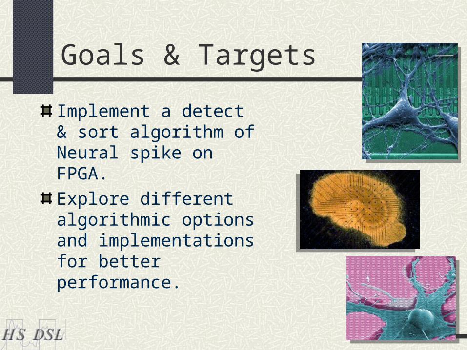
Requirements
Low frequency: ~100KHz input rate.
Small H/W as possible
Very low power consumption
Low output rate as possible

Algorithm overview
Learning phase: Apply PCA algorithm on a set of learning data Extract best separation lines from the learning data. Store separation lines parameters in chip registers.

Algorithm overview
Real time sorting: Apply threshold detection to raw data Calculate speculative projections on PC space,
for a set of predefined alignments. Find the most suitable alignment (maximum
find) Sort the spike by comparing to separation lines

Algorithm overview

Interface
TOP
OPMode[3]
SpikeData[5]
DataV[1]
CRDataIn[8]
Time[??]
PCSel[1]
SpikeID[2]
RST
CLK
OutV[1]
TimeStamp[??]
CRDataOut[8]
CRAddrIn[4]

Operation modes
LDPC mode: In this mode PC data is loaded into internal registers. The data is input on the SPKDATA pin, and the PC index is set by PCSEL pin (‘0’ – PC1, ‘1’ – PC2). The registers depth is the same as the spike length.
WRCR mode: In this mode the unit updates the control register with address on pin CRADDR with the value on pin CRDATA.
RDCR mode: In this mode the value in the CR with address on pin CRADD is written to output pin CRDATAOUT
SORT mode: In this mode unit sorts the spike data on pin SPKDATA.
IDLE mode: In this mode no operation is done in the unit. CR values are kept.
RST

Implementation
Block diagram:
CTL
SRT
SPKData
CR
DataIn
CRDataOut
OutV
SPKIdOut
EXT
DET
Controls
Time stamp
Tim
e

Implementation
Detection block:
CMP
SpikeData(from IO)
Threshold(from CTL)
PrevTRIG Value
CNT
Trig(to CTL)

Implementation
Extraction block:
SpikeData(from IO) 19
6 01
196 01
X +
196 01
X +
0
59
0
59
FINDMAX
Proj1(to SRT)
Proj2(to SRT)

Implementation
Sorting block:
X +
Proj2(from EXT)
ID(to IO)CMP ID
ENC
Proj1(from EXT)

Implementation
Control block:
CRG
MODEDEC
TIMER
EXTCTL
SRTCTL
OPMOD
CRDataIn
DETCTL

Implementation
Pipeline diagram
I/O DetectProjCalc
MaxFind
ProjRead
Sort I/O
X196 X60 X2
SO
RT
mo
de
I/OShiftPCR
LDP
C m
ode
Implementation
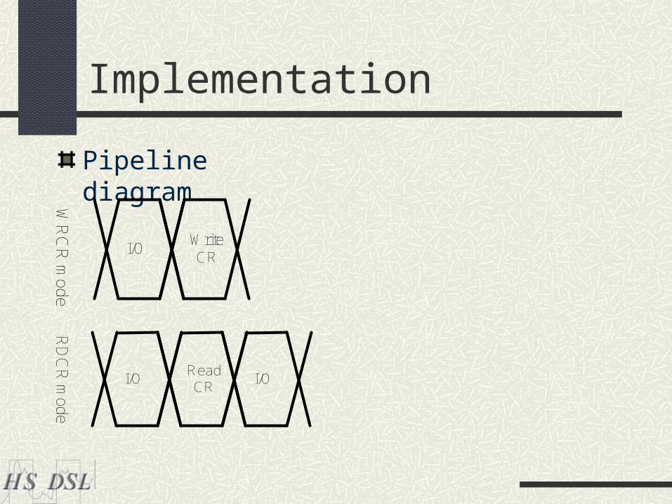
Pipeline diagram
I/OWriteCR
WR
CR
mo
de
I/OReadCR
I/O
RD
CR
mode

H/W characterization
100KHz input rate 20MHz internal clock freq.
40 input data pins
27 output pins
W/C output rate: 500Hz x 19 pins
# of logic gates: ???
# of seq. elements: ~5K

Environment
FPGA
tb_control
Spike &PCV data
reader
Sortparameters
reader
OPMOD[3]
trig
clk
clk
clk
clk
Send_par_done
Send_spk_done
Send_spk_doneS
end_spk
Send_param
resetreset
reset
reset
spike_data[5]
DataV[1]
CR
DataIn[8]
Tim
e[16]
SpikeID[2]
OutV[1]
TimeStamp[16]
CRDataOut[8]
CR
AddrIn[4]
Resultschecker
clk
reset

Current status
HDL code written
Only partly validated.
Environment almost ready (for HDL model)

Till end of Jan: Validation finished First simulation Initial syn runs Initial P&R H/W order Validation finished
February – Asaf in RD
Future time line

Back up Foils