SPICE Diode and BJT models
34
Department of Electrical and Electronic Engineering Imperial College London EE 2.3: Semiconductor Modelling in SPICE Course homepage: http://www.imperial.ac.uk/people/paul.mitcheson/teaching SPICE Diode and BJT models Paul D. Mitcheson [email protected] Room 1111, EEE EE2.3 Semiconductor Modelling in SPICE / PDM – v1.0 1
Transcript of SPICE Diode and BJT models
Department of Electrical and Electronic Engineering Imperial College London
EE 2.3: Semiconductor Modelling in SPICE Course homepage: http://www.imperial.ac.uk/people/paul.mitcheson/teaching
SPICE Diode and BJT models Paul D. Mitcheson [email protected]
Room 1111, EEE
EE2.3 Semiconductor Modelling in SPICE / PDM – v1.0 1

1. Summary of last lecture We saw that: • SPICE deals with current sources not voltage sources
• Gaussian elimination is used to solve the equations
• Newton-Raphson is used to solve circuits with non-linear elements
• There is a convergence aid, called GMIN, which aids convergence of the Newton-
Raphson algorithm by eliminating divide by zero errors
EE2.3 Semiconductor Modelling in SPICE / PDM – v1.0 2
2. Today’s lecture We will look at: • SPICE large signal diode model
• DC and large signal transient models
• SPICE large signal BJT model
• DC and large signal transient models
• The parameters of these models and how they relate to the device physics you know
EE2.3 Semiconductor Modelling in SPICE / PDM – v1.0 3

3.
3.1.
The SPICE Diode Model
DC Model The simple DC equation you know is the well known Shockley equation, that is:
⎥⎦
⎤⎢⎣
⎡−⎟⎟
⎠
⎞⎜⎜⎝
⎛= 1exp
tsD V
VII
Where IS is the diode’s reverse saturation current, V is the applied voltage bias, Vt is the thermal voltage (equal to kT/q which is about 25mV at room temperature) and ID is the current through the device.
EE2.3 Semiconductor Modelling in SPICE / PDM – v1.0 4

The simple DC model used in SPICE is very similar to the Shockley equation, with the addition of a parameter n, and a convergence aid of a the GMIN parallel conductance (see Error! Reference source not found.). The basic static diode model equation is thus:
GMINVnVVII D
tsD +⎥
⎦
⎤⎢⎣
⎡−⎟⎟
⎠
⎞⎜⎜⎝
⎛= 1exp
⎥⎦
⎤⎢⎣
⎡−⎟⎟
⎠
⎞⎜⎜⎝
⎛= 1exp
tsD nV
VII
EE2.3 Semiconductor Modelling in SPICE / PDM – v1.0 5
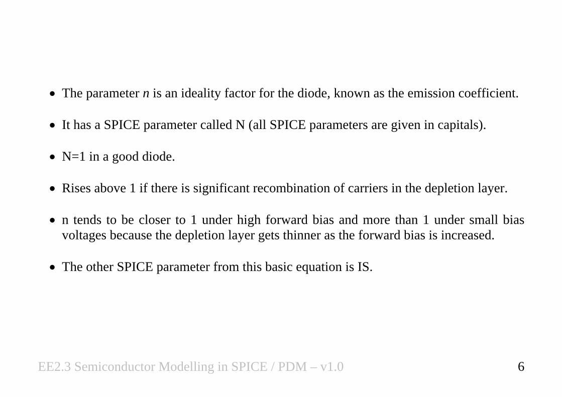
• The parameter n is an ideality factor for the diode, known as the emission coefficient.
• It has a SPICE parameter called N (all SPICE parameters are given in capitals).
• N=1 in a good diode.
• Rises above 1 if there is significant recombination of carriers in the depletion layer.
• n tends to be closer to 1 under high forward bias and more than 1 under small bias
voltages because the depletion layer gets thinner as the forward bias is increased. • The other SPICE parameter from this basic equation is IS.
EE2.3 Semiconductor Modelling in SPICE / PDM – v1.0 6

• In order to allow faster simulations than this equation would provide, a simple approximation is made in moderate reverse bias.
• When VD<-5nVt, SPICE uses the assumption that the leakage current through the p-n
junction is simply equal to IS, rather than actually calculating the exact exponential term.
• This means that under these conditions the total current through the complete static
SPICE diode model is:
GMINVII DsD +−= What is a physical meaning of IS?
EE2.3 Semiconductor Modelling in SPICE / PDM – v1.0 7

It is the limit of the current in the diode under high reverse bias. If the diode did not exhibit breakdown, the maximum reverse current that you could get through the diode with an infinite reverse bias would be Is. • You can now appreciate why the GMIN component is vital in achieving convergence
in the region of VD<-5nVt, because the conductance would otherwise be zero in that region.
EE2.3 Semiconductor Modelling in SPICE / PDM – v1.0 8

• SPICE includes breakdown in the model, and is modelled as an exponential breakdown past a certain voltage, the breakdown voltage, specified as SPICE parameter BV, with current at breakdown of IBV.
The current after breakdown is modelled with the following equation:
⎥⎦
⎤⎢⎣
⎡+−⎟⎟
⎠
⎞⎜⎜⎝
⎛ +−−=
VtBV
VVBVII
t
DSD 1exp
• When the diode voltage is equal to BV, the diode current as specified by this equation
is -IsBV/Vt. • It is therefore important that the SPICE parameter IBV (current at breakdown) is
somewhat near to -IsBV/Vt to allow continuity in the DC characteristic.
EE2.3 Semiconductor Modelling in SPICE / PDM – v1.0 9

DC curve implemented by SPICE
SPICE model DC diode characteristic split into 3 regions
EE2.3 Semiconductor Modelling in SPICE / PDM – v1.0 10

Finally, a series resistance is added to the diode model to simulate the resistances of the connecting wires and the ohmic contact resistances, giving us the following simple static model:
Figure 1 Static DC diode model
RSIVV DDD +=' And so,
EE2.3 Semiconductor Modelling in SPICE / PDM – v1.0 11

In summary, the important SPICE parameters (given in capitals and corresponding to the physical parameters in italics) for setting the DC characteristic are: IS (Is) The reverse saturation current RS (Rs) The Ohmic resistance of the contacts and bond wires N (n) The emission (or ideality) coefficient BV The breakdown voltage (inputted to SPICE as a positive number) IBV The current at reverse breakdown (inputted to SPICE as a positive number)
With these parameters you can specify the complete static diode characteristic.
EE2.3 Semiconductor Modelling in SPICE / PDM – v1.0 12

3.1.1. Limitation of the Diode Model • The SPICE diode model does not include the effects of high level injection. • When deriving the Shockley equation you previously made the assumption that the
diode was operating in low-level injection. • In power semiconductors, this is not necessarily the case because they operate in what
is known as high level injection. • The SPICE model does not include this effect (because it was originally designed to
be used with low power signal devices).
EE2.3 Semiconductor Modelling in SPICE / PDM – v1.0 13

3.2. Large Signal Transient Model • We now need to add dynamic effects to the diode model • Add capacitances to the model
Figure 2 SPICE Large signal transient model
EE2.3 Semiconductor Modelling in SPICE / PDM – v1.0 14

Capacitance Calculation Two contributions to capacitance between the terminals of a diode. • diffusion capacitance • depletion (or junction) capacitance.
Depletion (junction) capacitance, dominant in reverse bias, is given by:
))((2 0 VVNNNeNACDA
DAj −+=
εε
How did we calculate this capacitance? Why does it increase as V increases?
EE2.3 Semiconductor Modelling in SPICE / PDM – v1.0 15

SPICE implements essentially the same equation, but written slightly differently… Rewrite this:
0
0
1
1)(2
VVNN
VNeNACDA
DAj
−+=
ε
Which can again be written as:
0
1
)0(
VV
CC j
j
−=
This is the equation SPICE uses to calculate the depletion capacitance, where Cj(o) is the junction capacitance at zero applied bias and is the SPICE parameter CJ0. What is the physical meaning of CJ0?
EE2.3 Semiconductor Modelling in SPICE / PDM – v1.0 16

• The diffusion capacitance, Cd, is dominant in forward bias. • capacitance associated with the stored minority carriers in neutral regions.
τIkTeCd =
SPICE uses the same equation, but adds in the diode ideality coefficient:
τInkT
eCd =
What is the relation of Cd with device voltage? Intuitively, why is this?
EE2.3 Semiconductor Modelling in SPICE / PDM – v1.0 17

Dynamic SPICE diode model parameters
CJ0 (Cj(0)) Zero bias junction capacitance The transit time TT (τ) Built in junction voltage VJ (V0)
• You now know the most important parameters to allow you to specify a custom diode
model in SPICE. • There are a few more parameters which exist that we are not going to look at as we
have covered the important ones.
EE2.3 Semiconductor Modelling in SPICE / PDM – v1.0 18

3.3. A Note on the SPICE Area Parameter “A” and Device Scaling
SPICE has an area parameter called A, which can be used to scale any pn junction. The parameters IS, CJ0, RS and IBV are all proportional to device area. Two choices when entering these parameters: • Enter as parameters per unit cross sectional area and set the A parameter to the correct
cross sectional area of the device • Enter them as the values for a specific device and set the Area value to 1. Then if you
want to have multiple devices in parallel, setting A=3 means your device will behave as if there were three devices in parallel.
EE2.3 Semiconductor Modelling in SPICE / PDM – v1.0 19

4. 4.1.
The SPICE BJT model DC model
We will use npn transistor for this analysis. SPICE uses the Ebers-Moll transistor model You know the following BJT equations:
⎥⎦
⎤⎢⎣
⎡−⎟⎟
⎠
⎞⎜⎜⎝
⎛= 1exp
t
besc V
VII
bc II β= cbe III += Why does SPICE not just use these equations?
EE2.3 Semiconductor Modelling in SPICE / PDM – v1.0 20

There are 2 versions of the Ebers-Moll model: • Injection model • Transport model SPICE uses transport model – but injection easier to understand
You are aware that a BJT is physically built as two back to back diodes, as shown below:
Why does it not behave like two back to back diodes?
EE2.3 Semiconductor Modelling in SPICE / PDM – v1.0 21
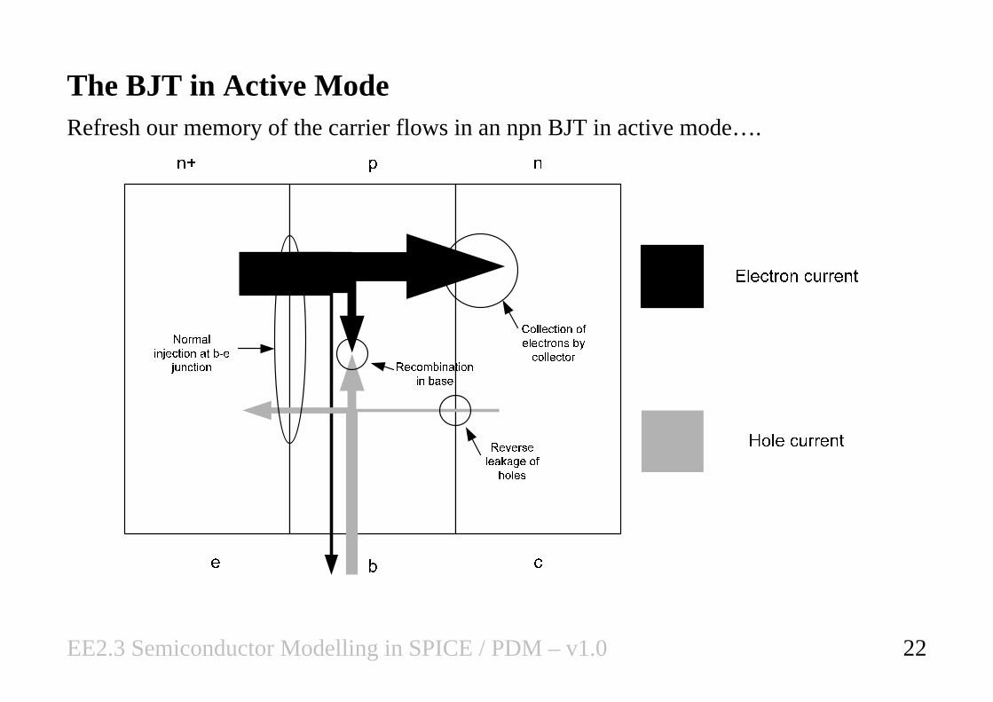
The BJT in Active Mode
Refresh our memory of the carrier flows in an npn BJT in active mode….
EE2.3 Semiconductor Modelling in SPICE / PDM – v1.0 22

The collector current is proportional to the concentration gradient of minority carriers in the base….
• In active mode, npc’ is approximately zero - the collector-base junction is reverse
biased. • emitter current is controlled completely by the base emitter voltage as this alters the
concentration gradient by altering npe’. EE2.3 Semiconductor Modelling in SPICE / PDM – v1.0 23

Can think of the BJT operating in this way as the following large signal equivalent circuit.
Where:
INbe – electron current through the base emitter junction IPbe – hole current through the base emitter junction IF – the total current through the base-emitter junction (INbe + IPbe) BF – fraction of electrons injected by the emitter which are collected by the collector (Neglect hole contribution to collector current)
EE2.3 Semiconductor Modelling in SPICE / PDM – v1.0 24

We will now define some terms which will allow us to simplify the diagram a little:
• The forward emitter injection efficiency, γF: Fraction of emitter current which comes from emission of electrons (for npn) or holes (for pnp) from the emitter. For an npn transistor, it is therefore:
PbeNbe
Nbe
e
NbeF II
II
I+
==γ
• The forward current transfer ratio, αF:
This is simply defined as:
e
cF I
I=α
EE2.3 Semiconductor Modelling in SPICE / PDM – v1.0 25

Assuming that the contribution of holes to the collector current is negligible:
NbeFc IBI ×= And thus:
γα FPbeNbe
NbeFF
e
c BII
IBII
=+
==
Thus, αF=BFγ Therefore:
EE2.3 Semiconductor Modelling in SPICE / PDM – v1.0 26

)( PbeNbeFFF IIBI += γα
)( PbeNbe
PbeNbe
NbeFFF II
IIIBI +⎟⎟
⎠
⎞⎜⎜⎝
⎛+
=∴α
And thus:
EE2.3 Semiconductor Modelling in SPICE / PDM – v1.0 27

NbeFFF IBI =α We can therefore write our equivalent circuit in terms of currents only, and not worry about what type of carrier makes up which current.
Much neater!
EE2.3 Semiconductor Modelling in SPICE / PDM – v1.0 28

The BJT in saturation Now let’s look at what happens to the device saturation. In saturation, both junctions are forward biased. If we look at the concentration of electrons in the device, we have:
Figure 3 BJT electron concentration in saturation
EE2.3 Semiconductor Modelling in SPICE / PDM – v1.0 29

Carrier flows in Saturation…
• Electron current decreased • Base current increased – holes injected into collector and emitter
EE2.3 Semiconductor Modelling in SPICE / PDM – v1.0 30

Look at the electron current… Can think of this as being made of a forward and a reverse flow of electrons (device in saturation in each case), due to the principle of linear superposition:
b
pcpet L
nnKI
''−=
b
pef L
nKI
'=
b
pcr L
nKI
'=
b
pcperft L
nnKIII
''−=−=
Where K is just a constant of proportionality and Lb is the length of the base
EE2.3 Semiconductor Modelling in SPICE / PDM – v1.0 31

Carrier flows with forward and reverse currents
EE2.3 Semiconductor Modelling in SPICE / PDM – v1.0 32
Summary of this lecture • The SPICE diode model is a piecewise non-linear function, which includes
breakdown • It is essential to have the GMIN convergence aid in that model because the
conductance of the diode is set to zero for much of the characteristic in reverse bias • The exponential equation you know for the behaviour of a BJT is not accurate in the
saturation region and so not useful (on its own) for a SPICE model • The started to look at the development of the Ebers Moll BJT model
• We can think of the currents in a saturated BJT as being a sum of forward and reverse
carrier flows in the base for equivalent forward and reverse BJTs operating in active mode
EE2.3 Semiconductor Modelling in SPICE / PDM – v1.0 33

Next time… • We will finish the Ebers-Moll model and see how it relates to the SPICE model
• We will look briefly at the SPICE MOSFET models
EE2.3 Semiconductor Modelling in SPICE / PDM – v1.0 34