SPI peripheral use case examples - Vorago Tech SPI block use... · AN1201 Version 1.0 SPI...
25
AN1201 Version 1.0 SPI peripheral use case examples Publish date: May 2016 Author: Clay Merritt Abstract This application note reviews the characteristics of an SPI bus and provides detailed software implementation descriptions for master mode operation. Three examples with increasing complexity demonstrate nearly all of the configuration options of the SPI block on the VA108xx series of microcontrollers. A software project (AN1201_SW.zip) accompanies this document with source code for demonstrating the examples. Table of Contents Abstract 1 SPI (Serial Peripheral Interface) overview 2 Vorago SPI peripheral register overview 3 Single byte frame example 6 Block mode with polling example 10 Block mode example with interrupts enabled 16 Running the demonstration program with examples 24 Common questions and issues 24
Transcript of SPI peripheral use case examples - Vorago Tech SPI block use... · AN1201 Version 1.0 SPI...

AN1201 Version 1.0
SPI peripheral use case examples
Publish date: May 2016
Author: Clay Merritt
Abstract
This application note reviews the characteristics of an SPI bus and provides detailed software
implementation descriptions for master mode operation. Three examples with increasing complexity
demonstrate nearly all of the configuration options of the SPI block on the VA108xx series of
microcontrollers. A software project (AN1201_SW.zip) accompanies this document with source code
for demonstrating the examples.
Table of Contents
Abstract 1
SPI (Serial Peripheral Interface) overview 2
Vorago SPI peripheral register overview 3
Single byte frame example 6
Block mode with polling example 10
Block mode example with interrupts enabled 16
Running the demonstration program with examples 24
Common questions and issues 24
2
SPI (Serial Peripheral Interface) overview
SPI is a four wire synchronous interface created by Motorola that has become a de facto standard for
serial communication. The SPI is normally used to connect two or more ICs that reside in the near
vicinity to each other. One device, the master, will initiate and control all the activity on the bus. The
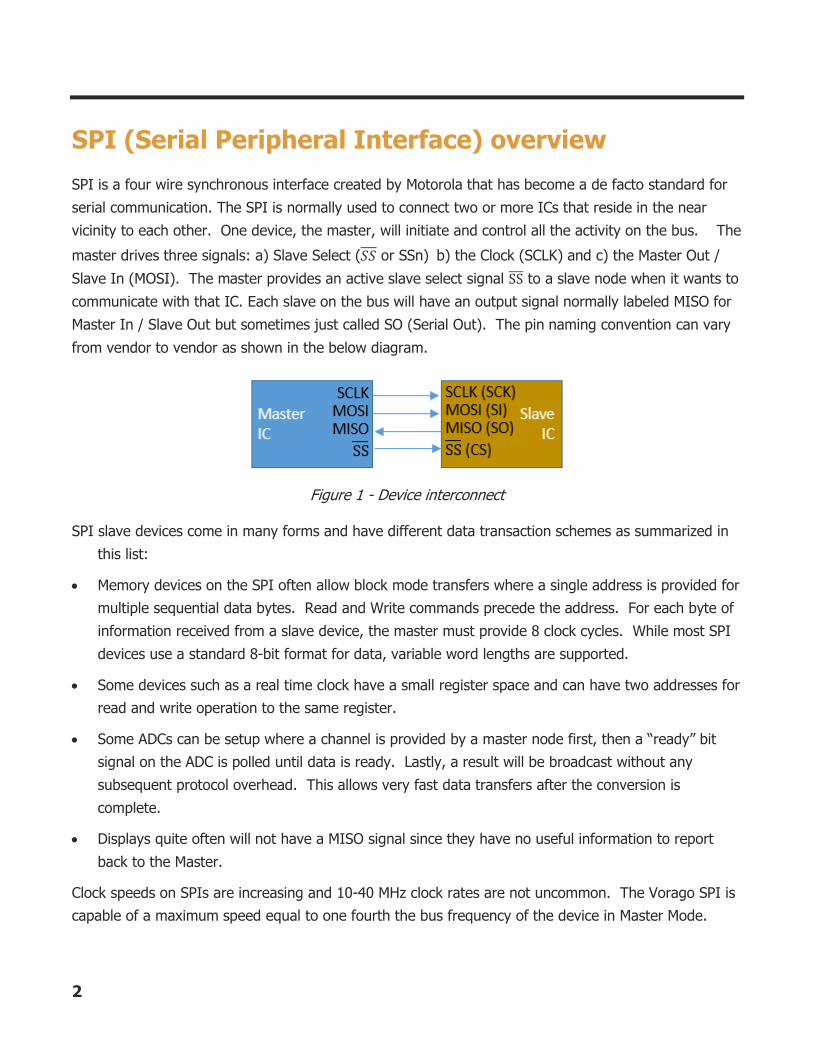
master drives three signals: a) Slave Select (𝑆𝑆 or SSn) b) the Clock (SCLK) and c) the Master Out /
Slave In (MOSI). The master provides an active slave select signal SS̅̅ ̅ to a slave node when it wants to
communicate with that IC. Each slave on the bus will have an output signal normally labeled MISO for
Master In / Slave Out but sometimes just called SO (Serial Out). The pin naming convention can vary
from vendor to vendor as shown in the below diagram.
Figure 1 - Device interconnect
SPI slave devices come in many forms and have different data transaction schemes as summarized in
this list:
Memory devices on the SPI often allow block mode transfers where a single address is provided for
multiple sequential data bytes. Read and Write commands precede the address. For each byte of
information received from a slave device, the master must provide 8 clock cycles. While most SPI
devices use a standard 8-bit format for data, variable word lengths are supported.
Some devices such as a real time clock have a small register space and can have two addresses for
read and write operation to the same register.
Some ADCs can be setup where a channel is provided by a master node first, then a “ready” bit
signal on the ADC is polled until data is ready. Lastly, a result will be broadcast without any
subsequent protocol overhead. This allows very fast data transfers after the conversion is
complete.
Displays quite often will not have a MISO signal since they have no useful information to report
back to the Master.
Clock speeds on SPIs are increasing and 10-40 MHz clock rates are not uncommon. The Vorago SPI is
capable of a maximum speed equal to one fourth the bus frequency of the device in Master Mode.
3
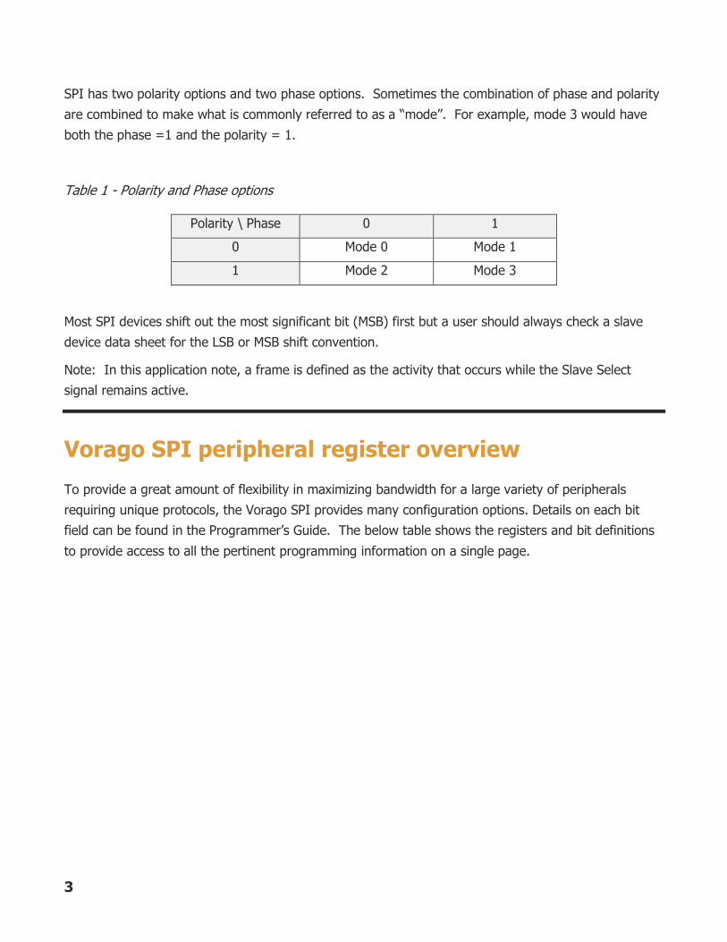
SPI has two polarity options and two phase options. Sometimes the combination of phase and polarity
are combined to make what is commonly referred to as a “mode”. For example, mode 3 would have
both the phase =1 and the polarity = 1.
Table 1 - Polarity and Phase options
Polarity \ Phase 0 1
0 Mode 0 Mode 1
1 Mode 2 Mode 3
Most SPI devices shift out the most significant bit (MSB) first but a user should always check a slave
device data sheet for the LSB or MSB shift convention.
Note: In this application note, a frame is defined as the activity that occurs while the Slave Select
signal remains active.
Vorago SPI peripheral register overview
To provide a great amount of flexibility in maximizing bandwidth for a large variety of peripherals
requiring unique protocols, the Vorago SPI provides many configuration options. Details on each bit
field can be found in the Programmer’s Guide. The below table shows the registers and bit definitions
to provide access to all the pertinent programming information on a single page.

4
Table 2 - SPI peripheral register list
Register bit location
31/23/15/7 30/22/14/6 29/21/13/5 28/20/12/4 27/19/11/3 26/18/10/2 25/17/9/1 24/16/8/0
CTRL0 31-24 -- -- -- -- -- -- -- --
23-16 -- -- -- -- -- -- -- --
15-8 SCRDIV
7-0 SPH SPO 0 0 SIZE
CTRL1 31-24 -- -- -- -- -- -- -- --
23-16 -- -- -- -- -- -- -- --
15-8 -- -- -- -- MTXPAUSE MDLYCAP BMSTALL BMSTART
7-0 BLOCKMODE SS SOD MS ENABLE LBM
DATA 31-24 BMSTART/BMSTOP
BMSKIPDATA -- -- -- -- -- --
23-16 -- -- -- -- -- -- -- --
15-8 VALUE (16 bits) 7-0
STATUS 31-24 -- -- -- -- -- -- -- --
23-16 -- -- -- -- -- -- -- --
15-8 -- -- -- -- -- -- -- --
7-0 TXTRIGGER RXTRIGGER RXDATAFIRST
BUSY RFF RNE TNF TFE
CLKPRESCALE 31-24 -- -- -- -- -- -- -- -- 23-16 -- -- -- -- -- -- -- -- 15-8 -- -- -- -- -- -- -- --
7-0 VALUE (7 bits) 0 IRQ_ENB 31-24 -- -- -- -- -- -- -- --
23-16 -- -- -- -- -- -- -- --
15-8 -- -- -- -- -- -- -- --
7-0 -- -- -- -- TXIM RXIM RTIM RORIM IRQ_RAW 31-24 -- -- -- -- -- -- -- --
23-16 -- -- -- -- -- -- -- --
15-8 -- -- -- -- -- -- -- --
7-0 -- -- -- -- TXIM RXIM RTIM RORIM IRQ_END 31-24 -- -- -- -- -- -- -- --
23-16 -- -- -- -- -- -- -- --
15-8 -- -- -- -- -- -- -- --
7-0 -- -- -- -- TXIM RXIM RTIM RORIM IRQ_CLR 31-24 -- -- -- -- -- -- -- --
23-16 -- -- -- -- -- -- -- --
15-8 -- -- -- -- -- -- -- --
7-0 -- -- -- -- -- -- RTIM RORIM RXFIFOIRQTRG 31-24 -- -- -- -- -- -- -- --
23-16 -- -- -- -- -- -- -- --
15-8 -- -- -- -- -- -- -- --
7-0 -- -- -- LEVEL (5 bits) TXFIFOIRQTRG 31-24 -- -- -- -- -- -- -- --
23-16 -- -- -- -- -- -- -- --
15-8 -- -- -- -- -- -- -- --
7-0 -- -- -- LEVEL (5 bits) FIFO_CLR 31-24 -- -- -- -- -- -- -- --
23-16 -- -- -- -- -- -- -- --
15-8 -- -- -- -- -- -- -- --
7-0 -- -- -- -- -- -- TXFIFO RXFIFO STATE 31-24 TXFIFO
23-16 ZERO
15-8 RXFIFO
7-0 RXSTATE
5
Notes on Examples
All the code can be found in AN1201_SW.zip. All three examples are included in one project.
The code was created for and tested on the VA108xx evaluation board – REB1. Full schematics, quick
start guides and more information can be found at Voragotech.com/REB1. Here is a summary of the
SPI connections on the REB1 board.
Example 1 and 3 uses a low cost 256-kbit Cypress SPI FRAM Arduino board (CY15FRAMKIT-001)
connected to SPIA with the following pin assignments.
SPI signal MCU pin name REB1 connector
SS SPI_SSELAn[0] -> PORTA[28] J9 - 8
MISO SPI_MISOA -> PORTA[29] J9 - 6
MOSI SPI_MOSIA -> PORTA[30] J9 - 7
SCK SPI_SCKA -> PORTA[31] J9 - 5
Example 2 uses 1-Mbit SPI EEPROM which is connected to SPIC which has the same pins as the
BOOTROM SPI. There are no PORTA or PORTB pins associated with these four signals.
SPI signal MCU pin name REB1 connector
SS ROM_SI Not available
MISO ROM_SO Not available
MOSI ROM_SCK Not available
SCK ROM_CS Not available
The example code will call out SPIA as “VOR_SPI->BANK[0]” and SPIC as “VOR_SPI->BANK[2]”.

6
Single byte frame example
While not the most common message frame, many applications use this type of transaction to
configure a device before heavy traffic activity occurs. To demonstrate the peripheral block in its
simplest form, this mode is explained in a three step process. The below figures show a timing diagram
and a scope capture of a single byte transfer. The scope capture shows a Write_Enable (0x06)
command for a memory device. There is nothing for the memory device to respond with and the MISO
pin (not shown) stays inactive at a low level.
Figure 2 - Simple single byte SPI frame
Figure 3 - Scope capture with SPI decode (Data = 0x06) information included.
7
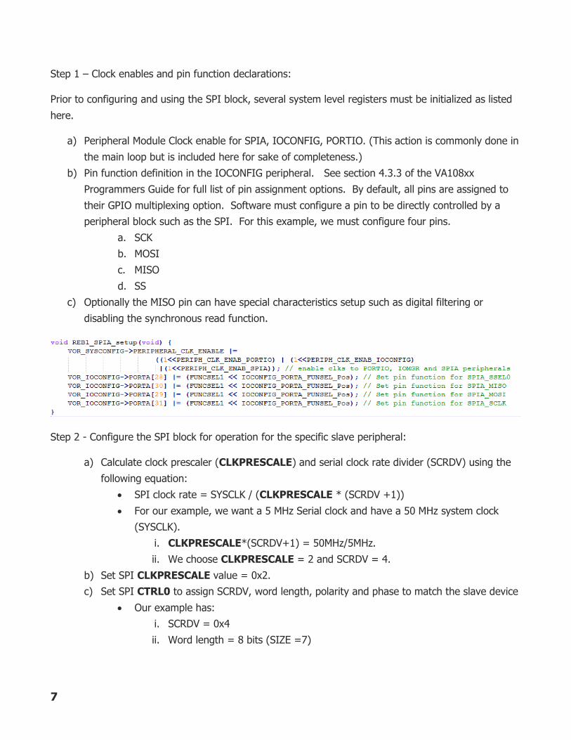
Step 1 – Clock enables and pin function declarations:
Prior to configuring and using the SPI block, several system level registers must be initialized as listed
here.
a) Peripheral Module Clock enable for SPIA, IOCONFIG, PORTIO. (This action is commonly done in
the main loop but is included here for sake of completeness.)
b) Pin function definition in the IOCONFIG peripheral. See section 4.3.3 of the VA108xx
Programmers Guide for full list of pin assignment options. By default, all pins are assigned to
their GPIO multiplexing option. Software must configure a pin to be directly controlled by a
peripheral block such as the SPI. For this example, we must configure four pins.
a. SCK
b. MOSI
c. MISO
d. SS
c) Optionally the MISO pin can have special characteristics setup such as digital filtering or
disabling the synchronous read function.
Step 2 - Configure the SPI block for operation for the specific slave peripheral:
a) Calculate clock prescaler (CLKPRESCALE) and serial clock rate divider (SCRDV) using the
following equation:
SPI clock rate = SYSCLK / (CLKPRESCALE * (SCRDV +1))
For our example, we want a 5 MHz Serial clock and have a 50 MHz system clock
(SYSCLK).
i. CLKPRESCALE*(SCRDV+1) = 50MHz/5MHz.
ii. We choose CLKPRESCALE = 2 and SCRDV = 4.
b) Set SPI CLKPRESCALE value = 0x2.
c) Set SPI CTRL0 to assign SCRDV, word length, polarity and phase to match the slave device
Our example has:
i. SCRDV = 0x4
ii. Word length = 8 bits (SIZE =7)

8
iii. SPO (Polarity) = 0
iv. SPH (Phase) = 0
d) Set CTRL1 register to select master mode, byte mode and the slave select number
MS = 0x0 (master = 0, slave = 1)
BLOCKMODE = 0x0 (byte mode = 0)
SS = 0x00
ENABLE = 0x1
Step 3 - Transmit data
a) Clear any stale data from both TX and RX FIFO
b) Set the Master transmit pause (MTXPAUSE) bit in CTRL1 to prevent any potential noise
glitches during FIFO load
c) Load the DATA TX FIFO with one word of data.
d) Clear MTX pause bit
e) Poll for transaction to be completed (optional “fire and forget” method is possible if no
immediate need for more SPI activity). Wait for SPIA to become not busy.
To demonstrate a couple more features of the SPI peripheral, a second frame is transmitted to read
the STATUS Register of the FRAM device. This will show how to transmit a word length other than 8
9
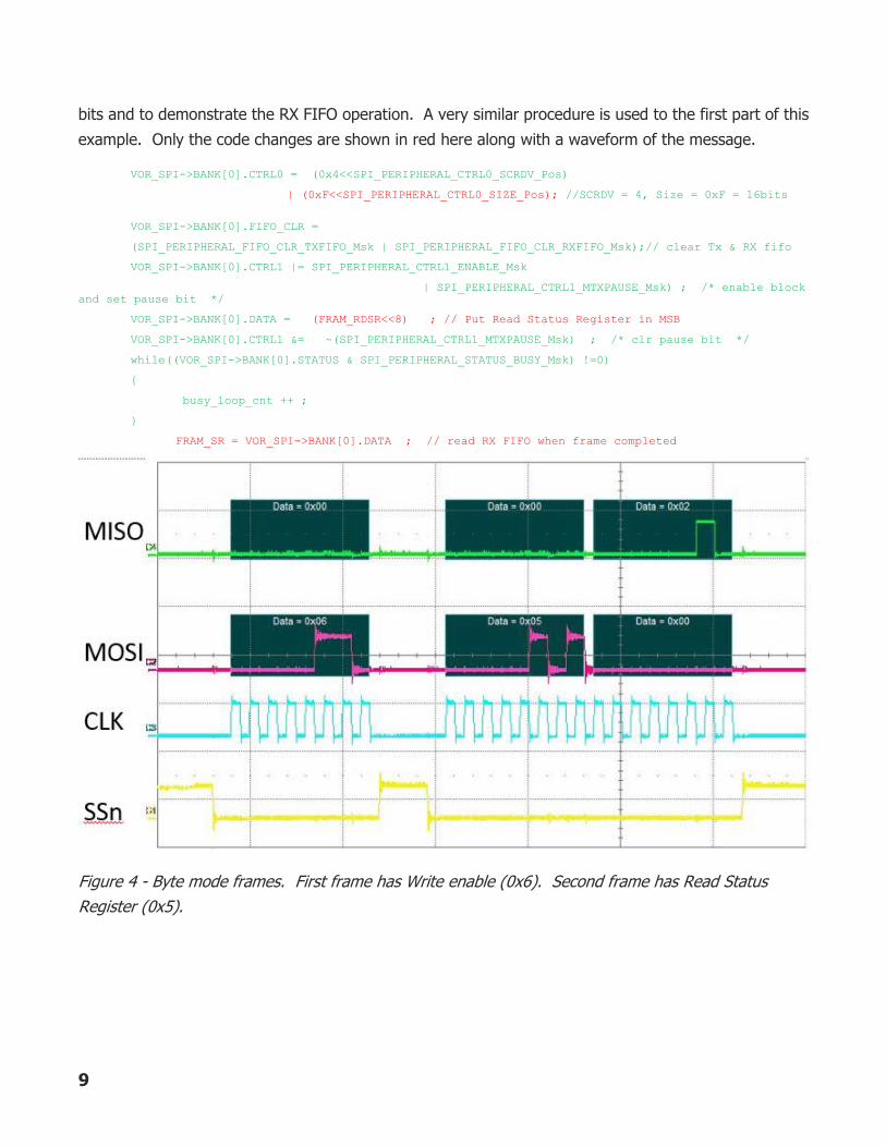
bits and to demonstrate the RX FIFO operation. A very similar procedure is used to the first part of this
example. Only the code changes are shown in red here along with a waveform of the message.
VOR_SPI->BANK[0].CTRL0 = (0x4<<SPI_PERIPHERAL_CTRL0_SCRDV_Pos)
| (0xF<<SPI_PERIPHERAL_CTRL0_SIZE_Pos); //SCRDV = 4, Size = 0xF = 16bits
VOR_SPI->BANK[0].FIFO_CLR =
(SPI_PERIPHERAL_FIFO_CLR_TXFIFO_Msk | SPI_PERIPHERAL_FIFO_CLR_RXFIFO_Msk);// clear Tx & RX fifo
VOR_SPI->BANK[0].CTRL1 |= SPI_PERIPHERAL_CTRL1_ENABLE_Msk
| SPI_PERIPHERAL_CTRL1_MTXPAUSE_Msk) ; /* enable block and set pause bit */
VOR_SPI->BANK[0].DATA = (FRAM_RDSR<<8) ; // Put Read Status Register in MSB
VOR_SPI->BANK[0].CTRL1 &= ~(SPI_PERIPHERAL_CTRL1_MTXPAUSE_Msk) ; /* clr pause bit */
while((VOR_SPI->BANK[0].STATUS & SPI_PERIPHERAL_STATUS_BUSY_Msk) !=0)
{
busy_loop_cnt ++ ;
}
FRAM_SR = VOR_SPI->BANK[0].DATA ; // read RX FIFO when frame completed
Figure 4 - Byte mode frames. First frame has Write enable (0x6). Second frame has Read Status
Register (0x5).

10
Block mode with polling example
The REB1 evaluation board has an SPI EEPROM connected to the ROM SPI lines. For this example, we
will read 32 bytes from the EEPROM in a single SPI frame using a block mode transfer and polling
method to keep the TX FIFO loaded and the RX FIFO from overflowing.
Figure 5 - SPI activity to read 32 bytes from SPI EEPROM
For maximum data transfer efficiency, minimizing command and header information is paramount. For
instance, it is possible to read a byte by sending the read command, 3 address bytes and then a single
dummy byte (only use of this byte is to supply a clock to receive data on the MISO pin) for a total of 5
bytes being transferred for a single byte read. Block mode allows a frame to continue for a limitless
number of clocks. This can support long streams of data reads while only transmitting the read
command and address information once. Two methods of block mode transfers are supported:
1. Using block mode stall (BMSTALL bit in CTRL1) and appending an end of Frame bit (BMSTOP)
on the last FIFO entry. This method allows the TXFIFO to run empty without terminating the
frame with the slave select line going inactive. The advantage to this method is that it is more
tolerant to delayed responses to SPI status flags.
2. Keeping the Transmit FIFO loaded with data and not allowing it to becomes empty until the
complete frame is transmitted.
We will use method 2 with polling in this example. The next example will use method 1 and interrupts.

11
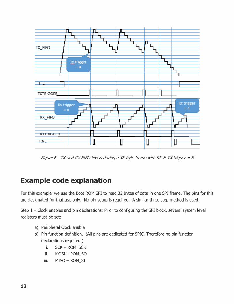
FIFO Control
Up to 16 words can be loaded into the Transmit FIFO before an overflow condition is created.
Similarly, up to 16 words can be received in the RX FIFO before an overflow condition occurs.
To allow options to trigger software to reload the Transmit FIFO, three event notices are provided.
1. TX FIFO “half empty” (TXTRIGGER bit in the STATUS register) {Associated with TXIM
interrupt}
2. TX FIFO empty (TFE bit) and
3. TX FIFO not full (TNF bit).
Each has a flag in the STATUS register available. Only the TX FIFO “half empty” condition has an
interrupt request (TXIM) associated with it.
The “half empty” level can be programmed to values between 1 and 16. Sometimes this type of
mechanism is referred to as a watermark. When the Transmit FIFO crosses the half empty threshold,
the TXTRIGGER status bit becomes active (level < TXFIFOIRQTRG). For this example, we will leave
TX trigger level at the default value of 8 and monitor it to gate TX FIFO load operations. This will allow
36 bytes to be transmitted in 4 TX FIFO load operations (16/8/8/4).
To trigger software to read the RX FIFO, three flags are available.
1. Rx FIFO “half full” (RXTRIGGER bit in the STATUS register) {Associated with RXIM interrupt}
2. Receive FIFO full flag (RFF bit) and
3. Receive FIFO not empty (RFE bit).
Only the RX FIFO “half full” trigger condition has an interrupt request (RXIM) associated with it.
We will use the RX FIFO “half full” trigger bit to prompt a read of the RX FIFO in this example. The
“half full” level (RXFIFOTRGIRQ=8) will be left at the default value of 8. This will allow the 36-byte
frame to be received in five unload/read operations (8/8/8/8/4).
The following diagram provides an illustration of the various status flags as they are set and cleared by
the SPI block during the frame being generated in this example.
12
Figure 6 - TX and RX FIFO levels during a 36-byte frame with RX & TX trigger = 8
Example code explanation
For this example, we use the Boot ROM SPI to read 32 bytes of data in one SPI frame. The pins for this
are designated for that use only. No pin setup is required. A similar three step method is used.
Step 1 – Clock enables and pin declarations: Prior to configuring the SPI block, several system level
registers must be set:
a) Peripheral Clock enable
b) Pin function definition. (All pins are dedicated for SPIC. Therefore no pin function
declarations required.)
i. SCK – ROM_SCK
ii. MOSI – ROM_SO
iii. MISO – ROM_SI
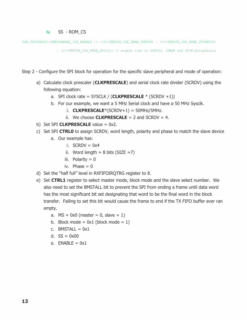
13
iv. SS - ROM_CS
VOR_SYSCONFIG->PERIPHERAL_CLK_ENABLE |= ((1<<PERIPH_CLK_ENAB_PORTIO) | (1<<PERIPH_CLK_ENAB_IOCONFIG)
| (1<<PERIPH_CLK_ENAB_SPIC)); // enable clks to PORTIO, IOMGR and SPIB peripherals
Step 2 - Configure the SPI block for operation for the specific slave peripheral and mode of operation:
a) Calculate clock prescaler (CLKPRESCALE) and serial clock rate divider (SCRDV) using the
following equation:
a. SPI clock rate = SYSCLK / (CLKPRESCALE * (SCRDV +1))
b. For our example, we want a 5 MHz Serial clock and have a 50 MHz Sysclk.
i. CLKPRESCALE*(SCRDV+1) = 50MHz/5MHz.
ii. We choose CLKPRESCALE = 2 and SCRDV = 4.
b) Set SPI CLKPRESCALE value = 0x2.
c) Set SPI CTRL0 to assign SCRDV, word length, polarity and phase to match the slave device
a. Our example has:
i. SCRDV = 0x4
ii. Word length = 8 bits (SIZE =7)
iii. Polarity = 0
iv. Phase = 0
d) Set the “half full” level in RXFIFOIRQTRG register to 8.
e) Set CTRL1 register to select master mode, block mode and the slave select number. We
also need to set the BMSTALL bit to prevent the SPI from ending a frame until data word
has the most significant bit set designating that word to be the final word in the block
transfer. Failing to set this bit would cause the frame to end if the TX FIFO buffer ever ran
empty.
a. MS = 0x0 (master = 0, slave = 1)
b. Block mode = 0x1 (block mode = 1)
c. BMSTALL = 0x1
d. SS = 0x00
e. ENABLE = 0x1
14
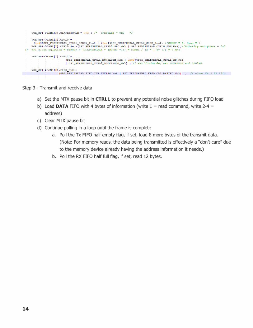
Step 3 - Transmit and receive data
a) Set the MTX pause bit in CTRL1 to prevent any potential noise glitches during FIFO load
b) Load DATA FIFO with 4 bytes of information (write 1 = read command, write 2-4 =
address)
c) Clear MTX pause bit
d) Continue polling in a loop until the frame is complete
a. Poll the Tx FIFO half empty flag, if set, load 8 more bytes of the transmit data.
(Note: For memory reads, the data being transmitted is effectively a “don’t care” due
to the memory device already having the address information it needs.)
b. Poll the RX FIFO half full flag, if set, read 12 bytes.

15
Advantages of polling method: Simplifies software development and in some cases the response time
to an event is improved.
Disadvantages of polling method: Can prevent (block) other software tasks from occurring and not
make productive use of CPU’s processing power while waiting for a frame to complete.

16
Block mode example with interrupts enabled
This example will be very similar to the polled block mode example above with the difference being
that the reload of the Transmit FIFO and read of the Receive FIFO are done inside of an interrupt
subroutine. This can free up the CPU to perform other duties until action is requested by the SPI
block.
Interrupt overview
The SPI block can generate 4 different interrupt requests. Each one has a dedicated bit in 4 separate
registers:
1) Enable - IRQ_EN,
2) Unqualified status - IRQ_RAW,
3) Status of enabled bits - IRQ_END, &
4) Clear interrupt flag - IRQ_CLR.
The four interrupts are OR’ed together before being routed to the IRQ selector peripheral. The IRQ
selector peripheral is needed to route and multiplex the >70 VA108xx interrupt sources to the 32 input
NVIC. The NVIC block sends an interrupt signal to the CPU and will provide a unique vector to a user
supplied interrupt subroutine. The IRQ Selector and NVIC blocks must be configured before any
signals pass through them.
Figure 7 - SPI interrupt path to CPU
17
RORIM (Receive overrun) and RTIM (Receive timeout) are error conditions and there should be code in
the SPI interrupt subroutine to handle errors. RXIM (RX FIFO at least half full) and TXIM (TX FIFO at
least half empty) are most often used to keep the FIFO loaded during extended frames as will be the
case in this example.
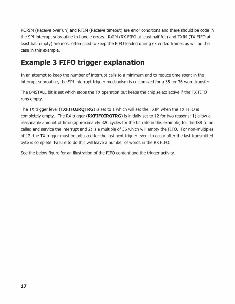
Example 3 FIFO trigger explanation
In an attempt to keep the number of interrupt calls to a minimum and to reduce time spent in the
interrupt subroutine, the SPI interrupt trigger mechanism is customized for a 35- or 36-word transfer.
The BMSTALL bit is set which stops the TX operation but keeps the chip select active if the TX FIFO
runs empty.
The TX trigger level (TXFIFOIRQTRG) is set to 1 which will set the TXIM when the TX FIFO is
completely empty. The RX trigger (RXFIFOIRQTRG) is initially set to 12 for two reasons: 1) allow a
reasonable amount of time (approximately 320 cycles for the bit rate in this example) for the ISR to be
called and service the interrupt and 2) is a multiple of 36 which will empty the FIFO. For non-multiples
of 12, the TX trigger must be adjusted for the last next trigger event to occur after the last transmitted
byte is complete. Failure to do this will leave a number of words in the RX FIFO.
See the below figure for an illustration of the FIFO content and the trigger activity.
18
Figure 8 - TX and RX FIFO levels during a 36 byte frame
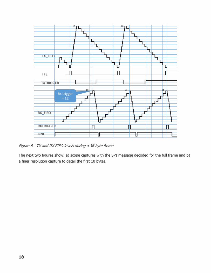
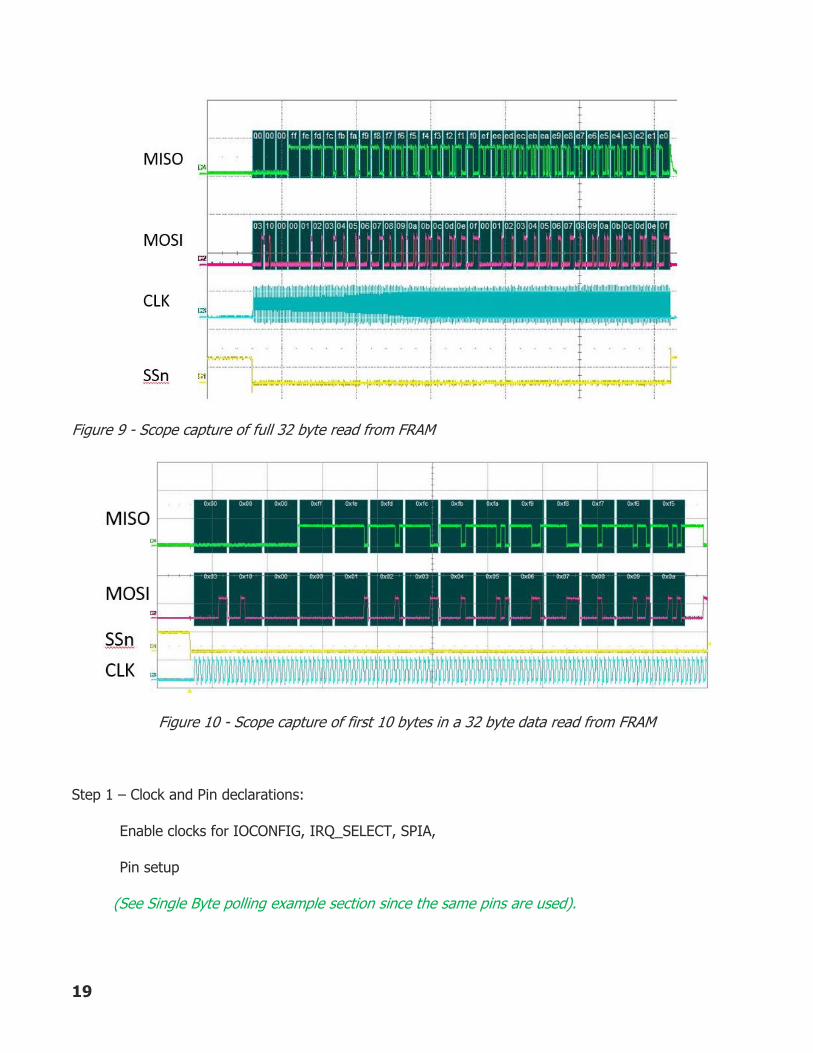
The next two figures show: a) scope captures with the SPI message decoded for the full frame and b)
a finer resolution capture to detail the first 10 bytes.
19
Figure 9 - Scope capture of full 32 byte read from FRAM
Figure 10 - Scope capture of first 10 bytes in a 32 byte data read from FRAM
Step 1 – Clock and Pin declarations:
Enable clocks for IOCONFIG, IRQ_SELECT, SPIA,
Pin setup
(See Single Byte polling example section since the same pins are used).
20
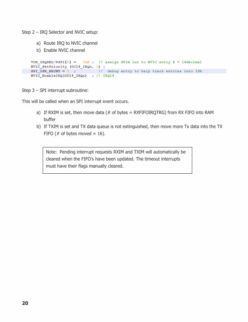
Step 2 – IRQ Selector and NVIC setup:
a) Route IRQ to NVIC channel
b) Enable NVIC channel
Step 3 – SPI interrupt subroutine:
This will be called when an SPI interrupt event occurs.
a) If RXIM is set, then move data (# of bytes = RXFIFOIRQTRG) from RX FIFO into RAM
buffer
b) If TXIM is set and TX data queue is not extinguished, then move more Tx data into the TX
FIFO (# of bytes moved = 16).
Note: Pending interrupt requests RXIM and TXIM will automatically be
cleared when the FIFO’s have been updated. The timeout interrupts
must have their flags manually cleared.

21
Step 4 - Configure the SPI block for operation for the specific slave peripheral:
a) Calculate clock prescaler (CLKPRESCALE) and serial clock rate divider (SCRDV) using the
following equation:
a. SPI clock rate = SYSCLK / (CLKPRESCALE * (SCRDV +1))
b. For our example, we want a 5 MHz Serial clock and have a 50 MHz Sysclk.
i. CLKPRESCALE*(SCRDV+1) = 50MHz/5MHz.
ii. We choose CLKPRESCALE = 2 and SCRDV = 4.
b) Set SPI CLKPRESCALE value = 0x2.
c) Set SPI CTRL0 to assign SCRDV, word length, polarity and phase to match the slave device
a. Our example has:
i. SCRDV = 0x4
ii. Word length = 8 bits (SIZE =7)

22
iii. Polarity = 0
iv. Phase = 0
d) Set the “half full” level in RXFIFOIRQTRG register to 12.
e) Set CTRL1 register to select master mode, block mode and the slave select number. We
also need to set the BMSTALL bit to prevent the SPI from ending a frame until data word
has the most significant bit set designating that word to be the final word in the block
transfer. Failing to set this bit would cause the frame to end if the TX FIFO buffer ever ran
empty.
a. MS = 0x0 (master = 0, slave = 1)
b. Block mode = 0x1 (block mode = 1)
c. BMSTALL = 0x1
d. SS = 0x00
e. ENABLE = 0x1
Step 5 - Transmit data
a) Put module in block mode and set MTXPAUSE bit in CTRL1
b) Load TX FIFO by writing to DATA
c) Enable module and Clear MTXPAUSE in CTRL1

23
Notes:
1. When using breakpoints with interrupts enabled, unpredictable results can occur. The CPU is
halted by the breakpoint but the peripheral continues to execute any action it has begun. Also
as the debugger refreshes the display window, the Data register for the FIFO can be read
which can essentially steal information that software may want to read at a later time.
2. When and when not to use interrupts is not always a clear cut decision. Variables that can
impact this are:
a. Bit rate of the SPI: Slower bit rates tend toward using interrupts so the SPI can be
processed in batches while still letting the main routine to be executed.
b. Other interrupts with higher priority: For systems using many interrupts for real time
events, using a polling method for servicing the SPI may be best.
c. Length of frame: Short frames (<8 words) can be handled more efficiently with a
polling method. The overhead of stacking registers for the interrupt can take 32 or
greater cycles by itself. For longer frames (>50 bytes) using the full depth of the FIFO
and interrupts will reduce the overall CPU demand for receiving or sending on the SPI.
3. Use of the watermark (RXFIFOIRQTRG & TXFIFOIRQTRG) for receive and transmit has
some debate behind it also. The purpose of this feature is to facilitate batch processing with
interrupts instead having to load or read each word as it is received or transmitted
respectively. Unless the full length of frame is known, using this feature can be complicated
due to the chance the FIFO will not hit the watermark prior to the frame being completed.

24
Running the demonstration program with examples
An accompanying file, AN1201_SW.zip has a complete project with all three examples. This software is
meant to run on the REB1 board and most likely would need to be altered to run on any other board to
match the pins and peripherals of that system.
The software was developed with the Keil MDK IDE. It may take some effort to adapt this project to
other IDEs.
Common questions and issues
1. Question: The slave device responds to a command but the MCU does not recognize the
information. What gives?
a. This often happens when the MCU polarity and phase settings do not match the slave
device’s. Check the data sheet of the peripheral device and set the MCU polarity and
phase bits appropriately.
2. Question: The MCU is transmitting bytes to a peripheral device but the device never responds.
What could be wrong?
a. There are many possibilities for this:
i. The slave select signal for the peripheral device is not properly connected is the
most common cause. Check that the MCU has the correct SS line enabled for
this frame
ii. The clock speed of the MCU SPI is greater than the slave device’s specified
maximum speed.
iii. Other enable pins on the slave device are not properly configured.
3. Question: I can see the slave device properly puts information on the MISO signal but the data
read from the Read buffer is 0xFF. What’s wrong?
a. Most likely this is an issue with the FIFO pointer not aligning with the intended data.
Every time the Master sends a byte of information out, it receives a byte of information
in the Receive buffer. For example, to read a memory location from a memory device
with over 65 kbytes, normally the transmit sequence will be Read_command, Adr_MSB,

25
Adr_MID, Adr_LSB, dummy character. The receive buffer will have four bytes of
information (most likely 0xFF or 0x00) prior to the read data. Software needs to be
cognizant of the read buffer content and discard unwanted information.
b. If the Receive buffer is not cleared prior to a frame it may have remnant information in
it. Best practice coding will always clear the FIFO before each frame.
4. Question: A master transmission starts correctly but is corrupted midway through the frame.
What is going on?
a. This situation can occur if a second frame is started before the first frame is complete.
Make sure software is either polling or triggering off the TX_FIFO empty interrupt before
starting another frame.
5. Question: My application has 9 slave devices and each requires its own chip select. How can I
get a ninth Slave select when only 8 are provided on the MCU?
a. There are three common solutions for this:
i. Use one of the other SPI blocks on the MCU to accommodate any peripheral
count greater than 8.
ii. Use a separate port pin to generate the chip select for the ninth device. It is
possible to disable the other chip selects from firing by deselecting the peripheral
pin function temporarily. Prior to starting a frame, drive the port pin low. When
the transmit buffer is empty, drive the port pin high.
iii. Use a multiplexor chip to direct the Slave select signal to the appropriate
peripheral device.
[End of AN1201]