Specification of 512M (16Mx32bit) Mobile...
54
This document is a general product description and is subject to change without notice. Hynix does not assume any responsibility for use of circuits described. No patent licenses are implied. Rev 1.5 / Jan. 2009 1 512MBit MOBILE SDR SDRAMs based on 4M x 4Bank x32 I/O Specification of 512M (16Mx32bit) Mobile SDRAM Memory Cell Array - Organized as 4banks of 4,194,304 x32
Transcript of Specification of 512M (16Mx32bit) Mobile...
This document is a general product description and is subject to change without notice. Hynix does not assume any responsibility for
use of circuits described. No patent licenses are implied.
Rev 1.5 / Jan. 2009 1
512MBit MOBILE SDR SDRAMs based on 4M x 4Bank x32 I/O
Specification of
512M (16Mx32bit) Mobile SDRAM
Memory Cell Array
- Organized as 4banks of 4,194,304 x32

Rev 1.5 / Jan. 2009 2
11512Mbit (16Mx32bit) Mobile SDR Memory
H55S5122DFR Series / H55S5132DFR Series
Document Title4Bank x 4M x 32bits Synchronous DRAM
Revision History
Revision No. History Draft Date Remark
0.1 Initial Draft Sep. 2007 Preliminary
0.2
Correction
- PKG Height: 1.0mm (without Ball Height)
-> 1.0mm (with Ball Height)
Feb. 2008 Preliminary
0.3 Update: IDD values Mar. 2008 Preliminary
1.0 Final Version Apr. 2008
1.1
-. Corrected the description of BURST TERMINATE
-. Corrected the CKE state on every command
-. Deleted the extended temperature products
May 2008
1.2 Modify : tRAS (166MHz/133Mhz: 42ns/45ns) Jun. 2008
1.3 Modify : tCK (CL=2, 166MHz [12ns -> 9.6ns]) Jul. 2008
1.4 Insert the reduced page Information Jul. 2008
1.5 Change the ball height (page 54) Jan. 2009
Rev 1.5 / Jan. 2009 3
11512Mbit (16Mx32bit) Mobile SDR Memory
H55S5122DFR Series / H55S5132DFR Series
DESCRIPTION
The Hynix H55S5122DFR is suited for non-PC application which use the batteries such as PDAs, 2.5G and 3G cellular
phones with internet access and multimedia capabilities, mini-notebook, hand-held PCs.
The Hynix 512M Mobile SDRAM is 536,870,912-bit CMOS Mobile Synchronous DRAM(Mobile SDR), ideally suited for the
main memory applications which requires large memory density and high bandwidth. It is organized as 4banks of
4,194,304x32.
Mobile SDRAM is a type of DRAM which operates in synchronization with input clock. The Hynix Mobile SDRAM latch
each control signal at the rising edge of a basic input clock (CLK) and input/output data in synchronization with the
input clock (CLK). The address lines are multiplexed with the Data Input/ Output signals on a multiplexed x32 Input/
Output bus. All the commands are latched in synchronization with the rising edge of CLK.
The Mobile SDRAMs provides for programmable read or write Burst length of Programmable burst lengths: 1, 2, 4, 8
locations or full page. An AUTO PRECHARGE function may be enabled to provide a self-timed row precharge that is ini-
tiated at the end of the burst access. The Mobile SDRAM uses an internal pipelined architecture to achieve high-speed
operation. This architecture is compatible with the 2n rule of prefetch architectures, but it also allows the column
address to be changed on every clock cycle to achieve a high-speed, fully random access. Precharging one bank while
accessing one of the other three banks will hide the precharge cycles and provide seamless, high-speed, random-
access operation.
Read and write accesses to the Hynix Mobile SDRAMs are burst oriented;
accesses start at a selected location and continue for a programmed number of locations in a programmed sequence.
Accesses begin with the registration of an ACTIVE command, which is then followed by a READ or WRITE command.
The address bits registered coincident with the ACTIVE command are used to select the bank and the row to be
accessed. The address bits registered coincident with the READ or WRITE command are used to select the bank and
the starting column location for the burst access. A burst of Read or Write cycles in progress can be terminated by a
burst terminate command or can be interrupted and replaced by a new burst Read or Write command on any
cycle(This pipelined design is not restricted by a 2N rule).
The Hynix Mobile SDR also provides for special programmable options including Partial Array Self Refresh of full array,
half array, quarter array Temperature Compensated Self Refresh of 45 or 85 degrees oC.
The Hynix Mobile SDR has the special Low Power function of Auto TCSR(Temperature Compensated Self Refresh) to
reduce self refresh current consumption. Since an internal temperature sensor is implanted, it enables to automatically
adjust refresh rate according to temperature without external EMRS command.
Deep Power Down Mode is a additional operating mode for Mobile SDR. This mode can achieve maximum power
reduction by removing power to the memory array within each Mobile SDR. By using this feature, the system can cut
off almost all DRAM power without adding the cost of a power switch and giving up mother-board power-line layout
flexibility.
All inputs are LV-CMOS compatible. Devices will have a VDD and VDDQ supply of 1.8V (nominal).

Rev 1.5 / Jan. 2009 4
11512Mbit (16Mx32bit) Mobile SDR Memory
H55S5122DFR Series / H55S5132DFR Series
INFORMATION for Hynix KNOWN GOOD DIE
With the advent of Multi-Chip package (MCPs), Package on Package (PoP) and system in a package (SiP) applications,
customer demand for Known Good Die (KGD) has increased.
Requirements for smaller form factors and higher memory densities are fueling the need for Wafer-level memory solu-
tions due to their superior flexibility. Hynix Known Good Die (KGD) products can be used in packaging technologies
such as systems-in-a-package (SIPs) and multi-chip packages (MCPs) to reduce the board area required, making them
ideal for hand-held PCs, and many other portable digital applications.
Hynix Mobile DRAM will be able to continue its constant effort of enabling the Advanced package products of all appli-
cation customers.
- Please Contact Hynix Office for Hynix KGD product availability and informations.
Rev 1.5 / Jan. 2009 5
11512Mbit (16Mx32bit) Mobile SDR Memory
H55S5122DFR Series / H55S5132DFR Series
FEATURES
Standard SDRAM Protocol
Clock Synchronization Operation
- All the commands registered on positive edge of basic input clock (CLK)
MULTIBANK OPERATION - Internal 4bank operation
- During burst Read or Write operation, burst Read or Write for a different bank is performed.
- During burst Read or Write operation, a different bank is activated and burst Read or Write
for that bank is performed
- During auto precharge burst Read or Write, burst Read or Write for a different bank is performed
Power Supply Voltage: VDD = 1.8V, VDDQ = 1.8V
LVCMOS compatible I/O Interface
Low Voltage interface to reduce I/O power
Programmable burst length: 1, 2, 4, 8 or full page
Programmable Burst Type: sequential or interleaved
Programmable CAS latency of 3 or 2
Programmable Drive Strength
Low Power Features
- Programmable PASR(Partial Array Self Refresh)
- Auto TCSR (Temperature Compensated Self Refresh)
- Programmable DS (Drive Strength)
- Deep Power Down Mode
Operation Temperature
- Mobile Temp.: -30oC ~ 85oC
Package Type: 90ball FBGA, 0.8mm pitch, 8 x 13 [mm2], t=1.0mm max, Lead & Halogen Free
512M SDRAM ORDERING INFORMATION
Part Number Clock FrequencyPage
SizeOrganization Interface Package
H55S5122DFR-60M 166MHz
2KBytes
(Normal)
4banks x 4Mb x 32 LVCMOS
90 Ball FBGA
Lead & Halogen
Free
H55S5122DFR-75M 133MHz
H55S5122DFR-A3M 105MHz
H55S5132DFR-60M 166MHz
1KBytes
(Reduced)H55S5132DFR-75M 133MHz
H55S5132DFR-A3M 105MHz

Rev 1.5 / Jan. 2009 6
11512Mbit (16Mx32bit) Mobile SDR Memory
H55S5122DFR Series / H55S5132DFR Series
BALL DESCRIPTION (A13 is used as 1KBytes reduced page)
91 2 3 4 6 7 8
TOPVIEW
DQ
26
DQ
24VSS VDD
DQ
23
DQ
21
DQ28
VDDQ VSSQ VDDQ VSSQ DQ19
VSSQ DQ27
DQ25
DQ22
DQ20
VDDQ
VSSQDQ29
DQ30
DQ17
DQ18
VDDQ
VDDQDQ31
NC NCDQ16
VSSQ
VSSDQM
3A3 A2
DQM2 VDD
A4 A5 A6 A10 A0 A1
A7 A8 A12 A13BA1
A11
CLK CKE A9BA
0/CS /RAS
DQM1
NC NC /CAS /WEDQM
0
A
B
C
D
E
F
G
H
J
K
VDDQDQ8
VSS VDDDQ7 VSSQ
VSSQDQ10
DQ9
DQ6
DQ5
VDDQ
VSSQDQ
12
DQ
14
DQ
1
DQ
3VDDQ
DQ11
VDDQ VSSQ VDDQ VSSQDQ4
DQ13
DQ15
VSS VDDDQ0
DQ2
L
M
N
P
R

Rev 1.5 / Jan. 2009 7
11512Mbit (16Mx32bit) Mobile SDR Memory
H55S5122DFR Series / H55S5132DFR Series
BALL DESCRIPTION
SYMBOL TYPE DESCRIPTION
CLK INPUTClock: The system clock input. All other inputs are registered to the SDRAM on the
rising edge of CLK
CKE INPUTClock Enable: Controls internal clock signal and when deactivated, the SDRAM will
be one of the states among power down, suspend or self refresh
CS INPUT Chip Select: Enables or disables all inputs except CLK, CKE, DQM0~DQM3
BA0, BA1 INPUTBank Address: Selects bank to be activated during RAS activity
Selects bank to be read/written during CAS activity
A0 ~ A13 INPUT
For 1KBytes Page Size, Row Address: RA0 ~ RA13, Column Address: CA0 ~ CA7
For 2KBytes Page Size, Row Address: RA0 ~ RA12, Column Address: CA0 ~ CA8
Auto-precharge flag: A10
RAS, CAS, WE INPUTCommand Inputs: RAS, CAS and WE define the operation
Refer function truth table for details
DQM0 ~ DQM3 INPUTData Mask: Controls output buffers in read mode and masks input data in write
mode
DQ0 ~ DQ31 I/O Data Input/Output: Multiplexed data input/output pin
VDD/VSS SUPPLY Power supply for internal circuits
VDDQ/VSSQ SUPPLY Power supply for output buffers
NC - No connection
Rev 1.5 / Jan. 2009 8
11512Mbit (16Mx32bit) Mobile SDR Memory
H55S5122DFR Series / H55S5132DFR Series
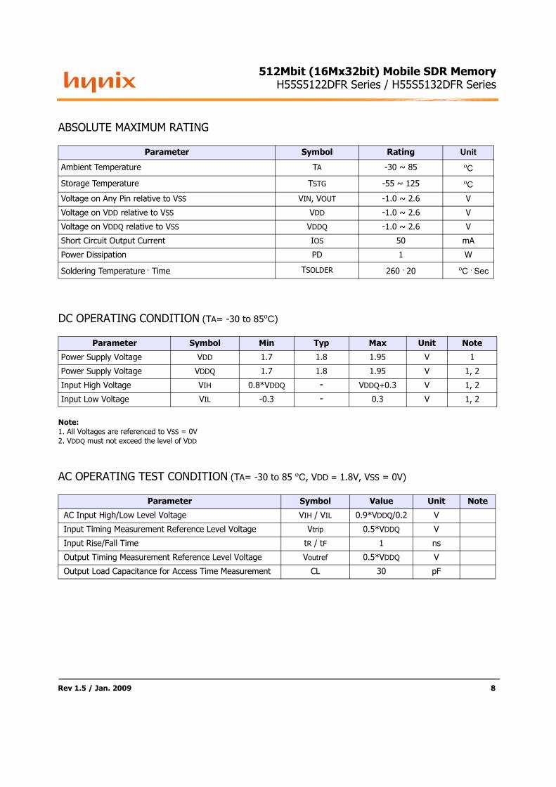
ABSOLUTE MAXIMUM RATING
DC OPERATING CONDITION (TA= -30 to 85oC)
Note:
1. All Voltages are referenced to VSS = 0V
2. VDDQ must not exceed the level of VDD
AC OPERATING TEST CONDITION (TA= -30 to 85 oC, VDD = 1.8V, VSS = 0V)
Parameter Symbol Rating Unit
Ambient Temperature TA -30 ~ 85 oC
Storage Temperature TSTG -55 ~ 125 oC
Voltage on Any Pin relative to VSS VIN, VOUT -1.0 ~ 2.6 V
Voltage on VDD relative to VSS VDD -1.0 ~ 2.6 V
Voltage on VDDQ relative to VSS VDDQ -1.0 ~ 2.6 V
Short Circuit Output Current IOS 50 mA
Power Dissipation PD 1 W
Soldering Temperature . Time TSOLDER 260 . 20 oC . Sec
Parameter Symbol Min Typ Max Unit Note
Power Supply Voltage VDD 1.7 1.8 1.95 V 1
Power Supply Voltage VDDQ 1.7 1.8 1.95 V 1, 2
Input High Voltage VIH 0.8*VDDQ - VDDQ+0.3 V 1, 2
Input Low Voltage VIL -0.3 - 0.3 V 1, 2
Parameter Symbol Value Unit Note
AC Input High/Low Level Voltage VIH / VIL 0.9*VDDQ/0.2 V
Input Timing Measurement Reference Level Voltage Vtrip 0.5*VDDQ V
Input Rise/Fall Time tR / tF 1 ns
Output Timing Measurement Reference Level Voltage Voutref 0.5*VDDQ V
Output Load Capacitance for Access Time Measurement CL 30 pF

Rev 1.5 / Jan. 2009 9
11512Mbit (16Mx32bit) Mobile SDR Memory
H55S5122DFR Series / H55S5132DFR Series
CAPACITANCE (TA= 25 oC, f=1MHz)
DC CHARACTERRISTICS I (TA= -30 to 85oC)
Note:
1. VIN = 0 to 1.8V. All other pins are not tested under VIN=0V.
2. DOUT is disabled. VOUT= 0 to 1.95V.
3. IOUT = - 0.1mA
4. IOUT = + 0.1mA
Parameter Pin Symbol6/H
UnitMin Max
Input capacitance
CLK CI1 2 4.0 pF
A0~A13, BA0, BA1, CKE, CS, RAS,
CAS, WE, DQM0~3 CI2 2 4.0 pF
Data input/output capacitance DQ0 ~ DQ31 CI/O 2 4.5 pF
Parameter Symbol Min Max Unit Note
Input Leakage Current ILI -1 1 uA 1
Output Leakage Current ILO -1 1 uA 2
Output High Voltage VOH VDDQ-0.2 - V 3
Output Low Voltage VOL - 0.2 V 4

Rev 1.5 / Jan. 2009 10
11512Mbit (16Mx32bit) Mobile SDR Memory
H55S5122DFR Series / H55S5132DFR Series
DC CHARACTERISTICS II (TA= -30 to 85oC)
Notes:
1. IDD1 and IDD4 depend on output loading and cycle rates. Specified values are measured with the output open
2. See the tables of next page for more specific IDD6 current values.
3. Please contact Hynix office for more information and ability for DPD operation.
Deep Power Down operation is a hynix optional function.
Parameter Symbol Test ConditionSpeed
Unit Note166MHz 133MHz 105MHz
Operating Current IDD1 Burst length=1, One bank active
tRC ≥ tRC(min), IOL=0mA60 45 45 mA 1
Precharge Standby
Current
in Power Down Mode
IDD2P CKE ≤ VIL(max), tCK = 15ns 0.3 mA
IDD2PS CKE ≤ VIL(max), tCK = ∞ 0.3 mA
Precharge Standby
Current
in Non Power Down
Mode
IDD2N
CKE ≥ VIH(min), CS ≥ VIH(min), tCK
= 15ns
Input signals are changed one time
during
2clks.
All other pins ≥ VDD-0.2V or ≤ 0.2V
5
mA
IDD2NS CKE ≥ VIH(min), tCK = ∞
Input signals are stable.1
Active Standby Current
in Power Down Mode
IDD3P CKE ≤ VIL(max), tCK = 15ns 5mA
IDD3PS CKE ≤ VIL(max), tCK = ∞ 3
Active Standby Current
in Non Power Down
Mode
IDD3N
CKE ≥ VIH(min), CS ≥ VIH(min), tCK
= 15ns
Input signals are changed one time
during
2clks.
All other pins ≥ VDD-0.2V or ≤ 0.2V
10
mA
IDD3NS CKE ≥ VIH(min), tCK = ∞
Input signals are stable.5
Burst Mode Operating
Current IDD4
tCK ≥ tCK(min), IOL=0mA
All banks active70 60 60 mA 1
Auto Refresh Current IDD5 tRFC ≥ tRFC(min) 100 mA
Self Refresh Current IDD6 CKE ≤ 0.2V See Next Page mA 2
Standby Current in
Deep Power Down
Mode
IDD7See the pages for the Deep Power
Down operation.10 uA 3
Rev 1.5 / Jan. 2009 11
11512Mbit (16Mx32bit) Mobile SDR Memory
H55S5122DFR Series / H55S5132DFR Series
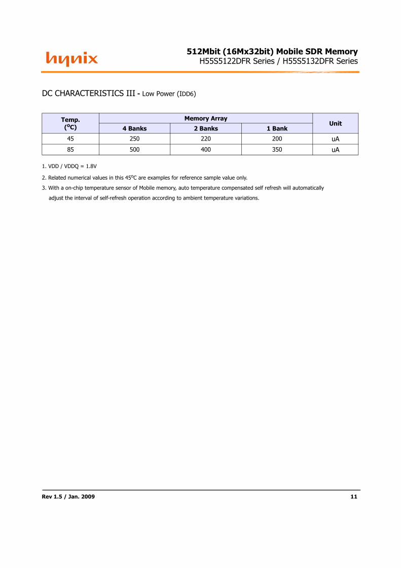
DC CHARACTERISTICS III - Low Power (IDD6)
1. VDD / VDDQ = 1.8V
2. Related numerical values in this 45oC are examples for reference sample value only.
3. With a on-chip temperature sensor of Mobile memory, auto temperature compensated self refresh will automatically
adjust the interval of self-refresh operation according to ambient temperature variations.
Temp.
(oC)
Memory ArrayUnit
4 Banks 2 Banks 1 Bank
45 250 220 200 uA
85 500 400 350 uA
Rev 1.5 / Jan. 2009 12
11512Mbit (16Mx32bit) Mobile SDR Memory
H55S5122DFR Series / H55S5132DFR Series
AC CHARACTERISTICS I (AC operating conditions unless otherwise noted)
Notes:
1. Assume tR / tF (input rise and fall time) is 1ns. If tR & tF> 1ns, then [(tR+tF)/2-1]ns should be added to the parameter.
2. Access time to be measured with input signals of 1V/ns edge rate, from 0.8V to 0.2V. If tR> 1ns, then (tR/2-0.5)ns
should be added to the parameter.
3. Output Load: 30pF+No termination
AC high level input voltage / low level input voltage: 1.6 / 0.2V
Input timing measurement reference level: 0.9V
Transition time (input rise and fall time): 0.5ns
Output timing measurement reference level: 0.9V
Output load: CL = 30pF
Parameter Symbol166MHz 133MHz 105MHz
Unit NoteMin Max Min Max Min Max
System Clock
Cycle Time
CAS Latency=3 tCK3 6.0 1000 7.5 1000 9.5 1000 ns
CAS Latency=2 tCK2 9.6 1000 12 1000 15 1000 ns
Clock High Pulse Width tCHW 2.0 - 2.5 - 3.0 - ns 1
Clock Low Pulse Width tCLW 2.0 - 2.5 - 3.0 - ns 1
Access Time From Clock CAS Latency=3 tAC3 - 5.4 - 6.0 - 7.0 ns 2, 3
CAS Latency=2 tAC2 - 6.0 - 8.0 - 10 ns 2, 3
Data-out Hold Time tOH 2.6 - 2.6 - 2.6 - ns 3
Data-Input Setup Time tDS 2.0 - 2.0 - 3.0 - ns 1
Data-Input Hold Time tDH 1.0 - 1.0 - 1.5 - ns 1
Address Setup Time tAS 2.0 - 2.0 - 3.0 - ns 1
Address Hold Time tAH 1.0 - 1.0 - 1.5 - ns 1
CKE Setup Time tCKS 2.0 - 2.0 - 3.0 - ns 1
CKE Hold Time tCKH 1.0 - 1.0 - 1.5 - ns 1
Command Setup Time tCS 2.0 - 2.0 - 3.0 - ns 1
Command Hold Time tCH 1.0 - 1.0 - 1.5 - ns 1
CLK to Data Output in Low-Z Time tOLZ 1.0 - 1.0 - 1.0 - ns
CLK to Data Output in
High-Z Time
CAS Latency=3 tOHZ3 5.4 6.0 7.0 ns
CAS Latency=2 tOHZ2 6.0 8.0 10 ns
Output
Z = 50Ω
30pF
Output Load
Output
tOH
tAC
tSETUP tHOLD
tCH tCL
tCK
1.6V
0.9V
0.2V
1.6V
0.9V
0.2V
Input
CLK
Rev 1.5 / Jan. 2009 13
11512Mbit (16Mx32bit) Mobile SDR Memory
H55S5122DFR Series / H55S5132DFR Series
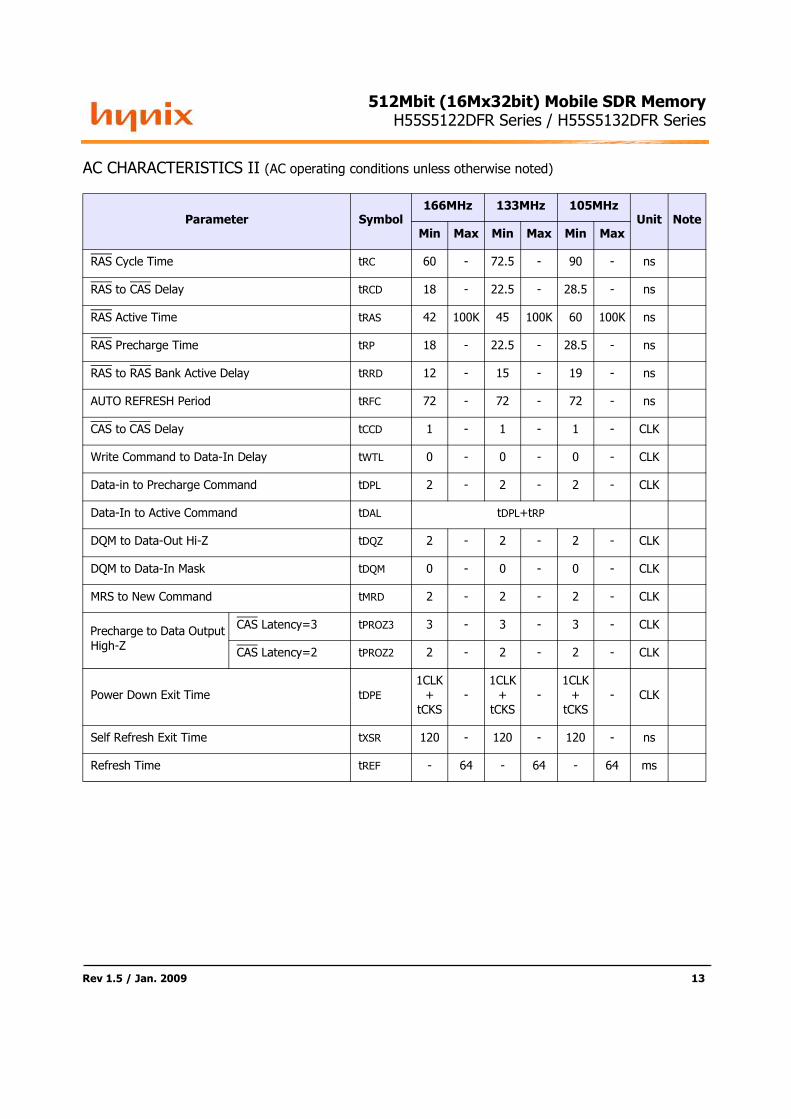
AC CHARACTERISTICS II (AC operating conditions unless otherwise noted)
Parameter Symbol166MHz 133MHz 105MHz
Unit NoteMin Max Min Max Min Max
RAS Cycle Time tRC 60 - 72.5 - 90 - ns
RAS to CAS Delay tRCD 18 - 22.5 - 28.5 - ns
RAS Active Time tRAS 42 100K 45 100K 60 100K ns
RAS Precharge Time tRP 18 - 22.5 - 28.5 - ns
RAS to RAS Bank Active Delay tRRD 12 - 15 - 19 - ns
AUTO REFRESH Period tRFC 72 - 72 - 72 - ns
CAS to CAS Delay tCCD 1 - 1 - 1 - CLK
Write Command to Data-In Delay tWTL 0 - 0 - 0 - CLK
Data-in to Precharge Command tDPL 2 - 2 - 2 - CLK
Data-In to Active Command tDAL tDPL+tRP
DQM to Data-Out Hi-Z tDQZ 2 - 2 - 2 - CLK
DQM to Data-In Mask tDQM 0 - 0 - 0 - CLK
MRS to New Command tMRD 2 - 2 - 2 - CLK
Precharge to Data Output
High-Z
CAS Latency=3 tPROZ3 3 - 3 - 3 - CLK
CAS Latency=2 tPROZ2 2 - 2 - 2 - CLK
Power Down Exit Time tDPE
1CLK
+
tCKS
-
1CLK
+
tCKS
-
1CLK
+
tCKS
- CLK
Self Refresh Exit Time tXSR 120 - 120 - 120 - ns
Refresh Time tREF - 64 - 64 - 64 ms

Rev 1.5 / Jan. 2009 14
11512Mbit (16Mx32bit) Mobile SDR Memory
H55S5122DFR Series / H55S5132DFR Series
FUNCTIONAL BLOCK DIAGRAM4Mbit x 4banks x 32 I/O Mobile Synchronous DRAM
(A13 is used as 1KBytes reduced page)
32
Internal RowCounter
ColumnPre
Decoder
Column AddCounter
Self refreshlog ic & timer
ExtendedMode
Register
Sense
AM
P &
I/O G
ate
Outp
ut B
uffe
r &
Logic
AddressRegister Burst
Counter
Mode Register
Sta
te M
ach
ine
Addre
ss Buffe
rs
Bank Select
Column Active
Row Active
CASLatency
CLK
CKE
CS
RAS
CAS
WE
DQM0 ~ 3
A0
A1
BA1
BA0
A13
PASR
RowPre
Decoder
RefreshDQ0
DQ31
Row d
eco
ders
Row d
eco
ders
Row d
eco
ders
Row d
eco
ders
Column decoders
4Mx32 BANK0
4Mx32 BANK1
4Mx32 BANK2
4Mx32 BANK3
MemoryCell
Array
Data Out Control
Burst
Length

Rev 1.5 / Jan. 2009 15
11512Mbit (16Mx32bit) Mobile SDR Memory
H55S5122DFR Series / H55S5132DFR Series
BASIC FUNCTIONAL DESCRIPTION
Mode Register (A13 is used as 1KBytes reduced page)
BA1 BA0 A13 A12 A11 A10 A9 A8 A7 A6 A5 A4 A3 A2 A1 A0
0 0 0 0 0 0 OP Code 0 0 CAS Latency BT Burst Length
OP Code
A9 Write Mode
0 Burst Read and Burst Write
1 Burst Read and Single Write
Burst Type
A3 Burst Type
0 Sequential
1 Interleave
Burst Length
A2 A1 A0Burst Length
A3 = 0 A3=1
0 0 0 1 1
0 0 1 2 2
0 1 0 4 4
0 1 1 8 8
1 0 0 Reserved Reserved
1 0 1 Reserved Reserved
1 1 0 Reserved Reserved
1 1 1 Full page Reserved
CAS Latency
A6 A5 A4 CAS Latency
0 0 0 Reserved
0 0 1 Reserved
0 1 0 2
0 1 1 3
1 0 0 Reserved
1 0 1 Reserved
1 1 0 Reserved
1 1 1 Reserved
Rev 1.5 / Jan. 2009 16
11512Mbit (16Mx32bit) Mobile SDR Memory
H55S5122DFR Series / H55S5132DFR Series
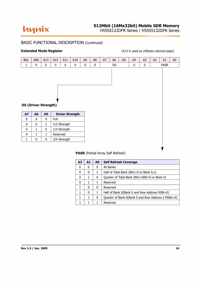
BASIC FUNCTIONAL DESCRIPTION (Continued)
Extended Mode Register (A13 is used as 1KBytes reduced page)
BA1 BA0 A13 A12 A11 A10 A9 A8 A7 A6 A5 A4 A3 A2 A1 A0
1 0 0 0 0 0 0 0 DS 0 0 PASR
DS (Driver Strength)
A7 A6 A5 Driver Strength
0 0 0 Full
0 0 1 1/2 Strength
0 1 0 1/4 Strength
0 1 1 Reserved
1 0 0 3/4 Strength
PASR (Partial Array Self Refresh)
A2 A1 A0 Self Refresh Coverage
0 0 0 All Banks
0 0 1 Half of Total Bank (BA1=0 or Bank 0,1)
0 1 0 Quarter of Total Bank (BA1=BA0=0 or Bank 0)
0 1 1 Reserved
1 0 0 Reserved
1 0 1 Half of Bank 0(Bank 0 and Row Address MSB=0)
1 1 0 Quarter of Bank 0(Bank 0 and Row Address 2 MSBs=0)
1 1 1 Reserved

Rev 1.5 / Jan. 2009 17
11512Mbit (16Mx32bit) Mobile SDR Memory
H55S5122DFR Series / H55S5132DFR Series
COMMAND TRUTH TABLE
Notes:
1. Exiting Self Refresh occurs by asynchronously bringing CKE from low to high.
2. BA1/BA0 must be issued 0/0 in the mode register set, and 1/0 in the extended mode register set.
Function CKEn-1 CKEn CS RAS CAS WE DQM ADDRA10
/APBA Note
Mode Register Set H X L L L L X Op Code 2
Extended Mode Register
SetH X L L L L X Op Code 2
No Operation H X L H H H X X
Device Deselect H X H X X X X X
Bank Active H X L L H H X Row Address V
Read H X L H L H Column L V
Read with Autoprecharge H X L H L H X Column H V
Write H X L H L L X Column L V
Write with Autoprecharge H X L H L L X Column H V
Precharge All Banks H X L L H L X X H X
Precharge selected Bank H X L L H L X X L V
Burst stop H X L H H L X X
Data Write/Output Enable H X X X X
Data Mask/Output Disable H X X V X
Auto Refresh H H L L L H X X
Self Refresh Entry H L L L L H X X
Self Refresh Exit L HH X X X
X X 1L H H H
Precharge Power Down
Entry H L
H X X XX X
L H H H
Precharge Power Down Exit L HH X X X
X XL H H H
Clock Suspend Entry H LH X X X
X XL V V V
Clock Suspend Exit L H X X X
Deep Power Down Entry H L L H H L X X
Deep Power Down Exit L H X X X
Rev 1.5 / Jan. 2009 18
11512Mbit (16Mx32bit) Mobile SDR Memory
H55S5122DFR Series / H55S5132DFR Series
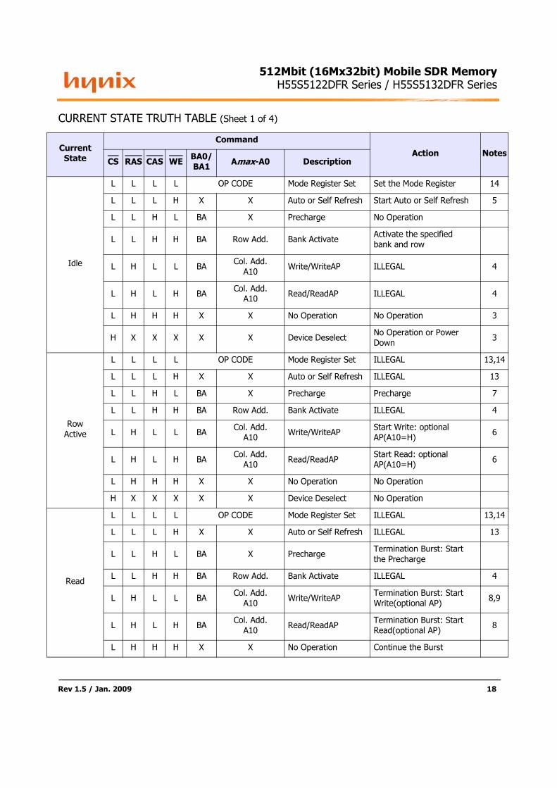
CURRENT STATE TRUTH TABLE (Sheet 1 of 4)
Current
State
Command
Action NotesCS RAS CAS WE
BA0/
BA1Amax-A0 Description
Idle
L L L L OP CODE Mode Register Set Set the Mode Register 14
L L L H X X Auto or Self Refresh Start Auto or Self Refresh 5
L L H L BA X Precharge No Operation
L L H H BA Row Add. Bank Activate Activate the specified
bank and row
L H L L BACol. Add.
A10 Write/WriteAP ILLEGAL 4
L H L H BACol. Add.
A10 Read/ReadAP ILLEGAL 4
L H H H X X No Operation No Operation 3
H X X X X X Device Deselect No Operation or Power
Down3
Row
Active
L L L L OP CODE Mode Register Set ILLEGAL 13,14
L L L H X X Auto or Self Refresh ILLEGAL 13
L L H L BA X Precharge Precharge 7
L L H H BA Row Add. Bank Activate ILLEGAL 4
L H L L BACol. Add.
A10 Write/WriteAP
Start Write: optional
AP(A10=H)6
L H L H BACol. Add.
A10 Read/ReadAP
Start Read: optional
AP(A10=H)6
L H H H X X No Operation No Operation
H X X X X X Device Deselect No Operation
Read
L L L L OP CODE Mode Register Set ILLEGAL 13,14
L L L H X X Auto or Self Refresh ILLEGAL 13
L L H L BA X Precharge Termination Burst: Start
the Precharge
L L H H BA Row Add. Bank Activate ILLEGAL 4
L H L L BACol. Add.
A10 Write/WriteAP
Termination Burst: Start
Write(optional AP)8,9
L H L H BACol. Add.
A10 Read/ReadAP
Termination Burst: Start
Read(optional AP)8
L H H H X X No Operation Continue the Burst
Rev 1.5 / Jan. 2009 19
11512Mbit (16Mx32bit) Mobile SDR Memory
H55S5122DFR Series / H55S5132DFR Series
CURRENT STATE TRUTH TABLE (Sheet 2 of 4)
Current
State
Command
Action NotesCS RAS CAS WE
BA0/
BA1Amax-A0 Description
Read H X X X X X Device Deselect Continue the Burst
Write
L L L L OP CODE Mode Register Set ILLEGAL 13,14
L L L H X X Auto or Self Refresh ILLEGAL 13
L L H L BA X Precharge Termination Burst: Start
the Precharge10
L L H H BA Row Add. Bank Activate ILLEGAL 4
L H L L BACol. Add.
A10 Write/WriteAP
Termination Burst: Start
Write(optional AP)8
L H L H BACol. Add.
A10 Read/ReadAP
Termination Burst: Start
Read(optional AP)8,9
L H H H X X No Operation Continue the Burst
H X X X X X Device Deselect Continue the Burst
Read with
Auto
Precharge
L L L L OP CODE Mode Register Set ILLEGAL 13,14
L L L H X X Auto or Self Refresh ILLEGAL 13
L L H L BA X Precharge ILLEGAL 4,12
L L H H BA Row Add. Bank Activate ILLEGAL 4,12
L H L L BA Col. Add. A10 Write/WriteAP ILLEGAL 12
L H L H BA Col. Add. A10 Read/ReadAP ILLEGAL 12
L H H H X X No Operation Continue the Burst
H X X X X X Device Deselect Continue the Burst
Write with
Auto
Precharge
L L L L OP CODE Mode Register Set ILLEGAL 13,14
L L L H X X Auto or Self Refresh ILLEGAL 13
L L H L BA X Precharge ILLEGAL 4,12
L L H H BA Row Add. Bank Activate ILLEGAL 4,12
L H L L BA Col. Add. A10 Write/WriteAP ILLEGAL 12
L H L H BA Col. Add. A10 Read/ReadAP ILLEGAL 12
L H H H X X No Operation Continue the Burst
H X X X X X Device Deselect Continue the Burst

Rev 1.5 / Jan. 2009 20
11512Mbit (16Mx32bit) Mobile SDR Memory
H55S5122DFR Series / H55S5132DFR Series
CURRENT STATE TRUTH TABLE (Sheet 3 of 4)
Current
State
Command
Action NotesCS RAS CAS WE
BA0/
BA1Amax-A0 Description
Precharging
L L L L OP CODE Mode Register Set ILLEGAL 13,14
L L L H X X Auto or Self Refresh ILLEGAL 13
L L H L BA X Precharge No Operation:
Bank(s) idle after tRP
L L H H BA Row Add. Bank Activate ILLEGAL 4,12
L H L L BA Col. Add. A10 Write/WriteAP ILLEGAL 4,12
L H L H BA Col. Add. A10 Read/ReadAP ILLEGAL 4,12
L H H H X X No Operation No Operation:
Bank(s) idle after tRP
H X X X X X Device Deselect No Operation:
Bank(s) idle after tRP
Row
Activating
L L L L OP CODE Mode Register Set ILLEGAL 13,14
L L L H X X Auto or Self Refresh ILLEGAL 13
L L H L BA X Precharge ILLEGAL 4,12
L L H H BA Row Add. Bank Activate ILLEGAL4,11,1
2
L H L L BA Col. Add. A10 Write/WriteAP ILLEGAL 4,12
L H L H BA Col. Add. A10 Read/ReadAP ILLEGAL 4,12
L H H H X X No Operation No Operation: Row
Active after tRCD
H X X X X X Device Deselect No Operation: Row
Active after tRCD
Write
Recovering
L L L L OP CODE Mode Register Set ILLEGAL 13,14
L L L H X X Auto or Self Refresh ILLEGAL 13
L L H L BA X Precharge ILLEGAL 4,13
L L H H BA Row Add. Bank Activate ILLEGAL 4,12
L H L L BA Col. Add. A10 Write/WriteAP Start Write:
Optional AP(A10=H)
L H L H BA Col. Add. A10 Read/ReadAP Start Read: Optional
AP(A10=H)9
L H H H X X No Operation No Operation:
Row Active after tDPL

Rev 1.5 / Jan. 2009 21
11512Mbit (16Mx32bit) Mobile SDR Memory
H55S5122DFR Series / H55S5132DFR Series
CURRENT STATE TRUTH TABLE (Sheet 4 of 4)
Current
State
Command
Action NotesCS RAS CAS WE
BA0/
BA1Amax-A0 Description
Write
RecoveringH X X X X X Device Deselect
No Operation:
Row Active after tDPL
Write
Recovering
with Auto
Precharge
L L L L OP CODE Mode Register Set ILLEGAL 13,14
L L L H X X Auto or Self Refresh ILLEGAL 13
L L H L BA X Precharge ILLEGAL 4,13
L L H H BA Row Add. Bank Activate ILLEGAL 4,12
L H L L BA Col. Add. A10 Write/WriteAP ILLEGAL 4,12
L H L H BA Col. Add. A10 Read/ReadAP ILLEGAL 4,9,12
L H H H X X No Operation No Operation:
Precharge after tDPL
H X X X X X Device Deselect No Operation:
Precharge after tDPL
Refreshing
L L L L OP CODE Mode Register Set ILLEGAL 13,14
L L L H X X Auto or Self Refresh ILLEGAL 13
L L H L BA X Precharge ILLEGAL 13
L L H H BA Row Add. Bank Activate ILLEGAL 13
L H L L BA Col. Add. A10 Write/WriteAP ILLEGAL 13
L H L H BA Col. Add. A10 Read/ReadAP ILLEGAL 13
L H H H X X No Operation No Operation:
idle after tRC
H X X X X X Device Deselect No Operation:
idle after tRC
Mode
Register
Accessing
L L L L OP CODE Mode Register Set ILLEGAL 13,14
L L L H X X Auto or Self Refresh ILLEGAL 13
L L H L BA X Precharge ILLEGAL 13
L L H H BA Row Add. Bank Activate ILLEGAL 13
L H L L BA Col. Add. A10 Write/WriteAP ILLEGAL 13
L H L H BA Col. Add. A10 Read/ReadAP ILLEGAL 13
L H H H X X No Operation No Operation:
idle after 2 clock cycles
H X X X X X Device Deselect No Operation:
idle after 2 clock cycles
Rev 1.5 / Jan. 2009 22
11512Mbit (16Mx32bit) Mobile SDR Memory
H55S5122DFR Series / H55S5132DFR Series
Notes:
1. H: Logic High, L: Logic Low, X: Don't care, BA: Bank Address, AP: Auto Precharge.
2. All entries assume that CKE was active during the preceding clock cycle.
3. If both banks are idle and CKE is inactive, then in power down cycle
4. Illegal to bank in specified states. Function may be legal in the bank indicated by Bank Address,
depending on the state of that bank.
5. If both banks are idle and CKE is inactive, then Self Refresh mode.
6. Illegal if tRCD is not satisfied.
7. Illegal if tRAS is not satisfied.
8. Must satisfy burst interrupt condition.
9. Must satisfy bus contention, bus turn around, and/or write recovery requirements.
10. Must mask preceding data which don't satisfy tDPL.
11. Illegal if tRRD is not satisfied
12. Illegal for single bank, but legal for other banks in multi-bank devices.
13. Illegal for all banks.
14. Mode Register Set and Extended Mode Register Set is same command truth table except BA1.

Rev 1.5 / Jan. 2009 23
11512Mbit (16Mx32bit) Mobile SDR Memory
H55S5122DFR Series / H55S5132DFR Series
CKE Enable(CKE) Truth TABLE (Sheet 2 of 1)
Current
State
CKE Command
Action NotesPrevi-
ous Cy-
cle
Current
CycleCS RAS CAS WE
BA0,
BA1
Amax-A0
Self
Refresh
H X X X X X X X INVALID 1
L H H X X X X X Exit Self Refresh with
Device Deselect2
L H L H H H X X Exit Self Refresh with
No Operation2
L H L H H L X X ILLEGAL 2
L H L H L X X X ILLEGAL 2
L H L L X X X X ILLEGAL 2
L L X X X X X X Maintain Self Refresh
Power
Down
H X X X X X X X INVALID 1
L HH X X X X X
Power Down mode exit,
all banks idle2
L H H H X X
L H L
L X X X X
ILLEGAL 2X L X X X
X X L X X
L L X X X X X X Maintain Power Down Mode
Deep
Power
Down
H X X X X X X X INVALID 1
L H X X X X X X Deep Power
Down mode exit5
L L X X X X X X Maintain Deep
Power Down Mode

Rev 1.5 / Jan. 2009 24
11512Mbit (16Mx32bit) Mobile SDR Memory
H55S5122DFR Series / H55S5132DFR Series
CKE Enable(CKE) Truth TABLE (Sheet 2 of 2)
Notes:
1. For the given current state CKE must be low in the previous cycle.
2. When CKE has a low to high transition, the clock and other inputs are re-enabled asynchronously.
When exiting power down mode, a NOP (or Device Deselect) command is required on the first positive edge of
clock after CKE goes high.
3. The address inputs depend on the command that is issued.
4. The Precharge Power Down mode, the Self Refresh mode, and the Mode Register Set can only be entered
from the all banks idle state.
5. When CKE has a low to high transition, the clock and other inputs are re-enabled asynchronously.
When exiting deep power down mode, a NOP (or Device Deselect) command is required on the first positive edge of
clock after CKE goes high and is maintained for a minimum 200usec.
Current
State
CKE Command
Action NotesPrevious
Cycle
Current
CycleCS RAS CAS WE
BA0,
BA1
Amax-A0
All
Banks
Idle
H H H X X X Refer to the idle State section
of the Current State
Truth Table
3
H H L H X X 3
H H L L H X 3
H H L L L H X X Auto Refresh
H H L L L L OP CODE Mode Register Set 4
H L H X X X Refer to the idle State section
of the Current State
Truth Table
3
H L L H X X 3
H L L L H X 3
H L L L L H X X Entry Self Refresh 4
H L L L L L OP CODE Mode Register Set
L X X X X X X X Power Down 4
Any State
other than
listed above
H H X X X X X X
Refer to operations of
the Current State
Truth Table
H L X X X X X X Begin Clock Suspend
next cycle
L H X X X X X X Exit Clock Suspend
next cycle
L L X X X X X X Maintain Clock Suspend

Rev 1.5 / Jan. 2009 25
11512Mbit (16Mx32bit) Mobile SDR Memory
H55S5122DFR Series / H55S5132DFR Series
Mobile SDR SDRAM OPERATIONState Diagram
ACT :Active
DPDS : Enter Deep Power-Down
DPDSX : Exit Deep Power-DownEMRS
EMRS : Ext. Mode Reg. Set
MRS : Mode Register Set
PRE : Precharge
PREALL : Precharge All Banks
REFA : Auto Refresh
REFS : Enter Self Refresh
REFSX : Exit Self Refresh
READ : Read w/o Auto Precharge
READA : Read with Auto Precharge
WRITE : Write w/o Auto Precharge
WRITEA : Write with Auto Precharge
IDLE
DEEPPOWER DOWN
PowerDown
ROWACTIVE
ACT
WRITEREAD
ActivePowerDown
WRITE with AP
READ with AP
WriteRead
READSUSPEND
READASUSPEND
WRITESUSPEND
WRITEASUSPEND
Read Write
WRITE
AREADA
PrechargeAll
Automatic Sequence
Manual input
CKE
HighCK
E
Low
CKE
Low
CKE
High
CKE High
CKE Lo
w
CKE Low
CKE H
igh
CKE Low
CKE Hi
gh
SelfRefresh
(EXTENDED)Mode Register
Set
AutoRefresh
PrechargeAll
Bank
PowerOn
REFA
REFS
REFX
(E)MRS
DPDS
DPDSX
PRE
PREPR
E
CKE Lo
w
CKE High
Rev 1.5 / Jan. 2009 26
11512Mbit (16Mx32bit) Mobile SDR Memory
H55S5122DFR Series / H55S5132DFR Series
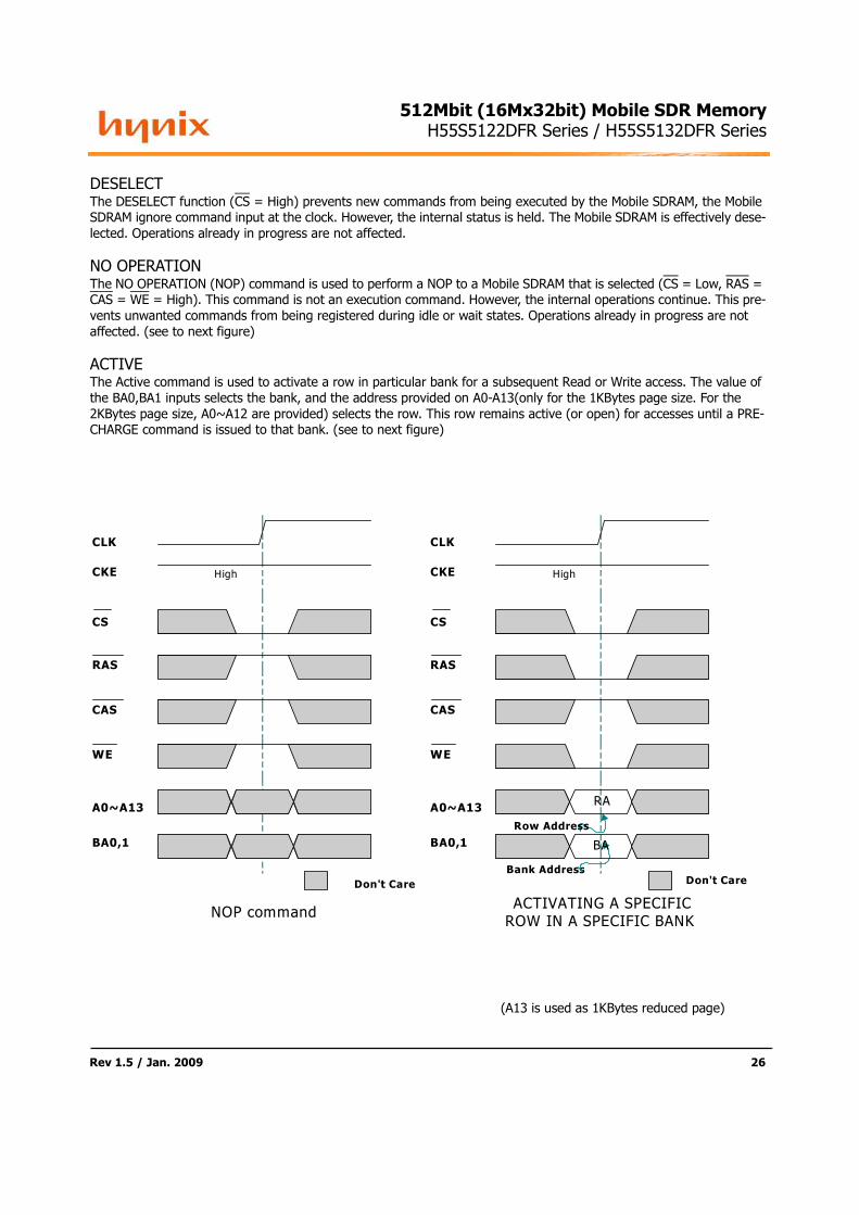
DESELECTThe DESELECT function (CS = High) prevents new commands from being executed by the Mobile SDRAM, the Mobile
SDRAM ignore command input at the clock. However, the internal status is held. The Mobile SDRAM is effectively dese-
lected. Operations already in progress are not affected.
NO OPERATIONThe NO OPERATION (NOP) command is used to perform a NOP to a Mobile SDRAM that is selected (CS = Low, RAS =
CAS = WE = High). This command is not an execution command. However, the internal operations continue. This pre-
vents unwanted commands from being registered during idle or wait states. Operations already in progress are not
affected. (see to next figure)
ACTIVEThe Active command is used to activate a row in particular bank for a subsequent Read or Write access. The value of
the BA0,BA1 inputs selects the bank, and the address provided on A0-A13(only for the 1KBytes page size. For the
2KBytes page size, A0~A12 are provided) selects the row. This row remains active (or open) for accesses until a PRE-
CHARGE command is issued to that bank. (see to next figure)
(A13 is used as 1KBytes reduced page)
CS
A0~A13
WE
CAS
RAS
Don't Care
CLK
CKE High
BA0,1
CS
A0~A13
WE
Bank Address
CAS
RAS
Row Address
Don't Care
CLK
CKE High
RA
BABA0,1
NOP command ACTIVATING A SPECIFIC ROW IN A SPECIFIC BANK
Rev 1.5 / Jan. 2009 27
11512Mbit (16Mx32bit) Mobile SDR Memory
H55S5122DFR Series / H55S5132DFR Series
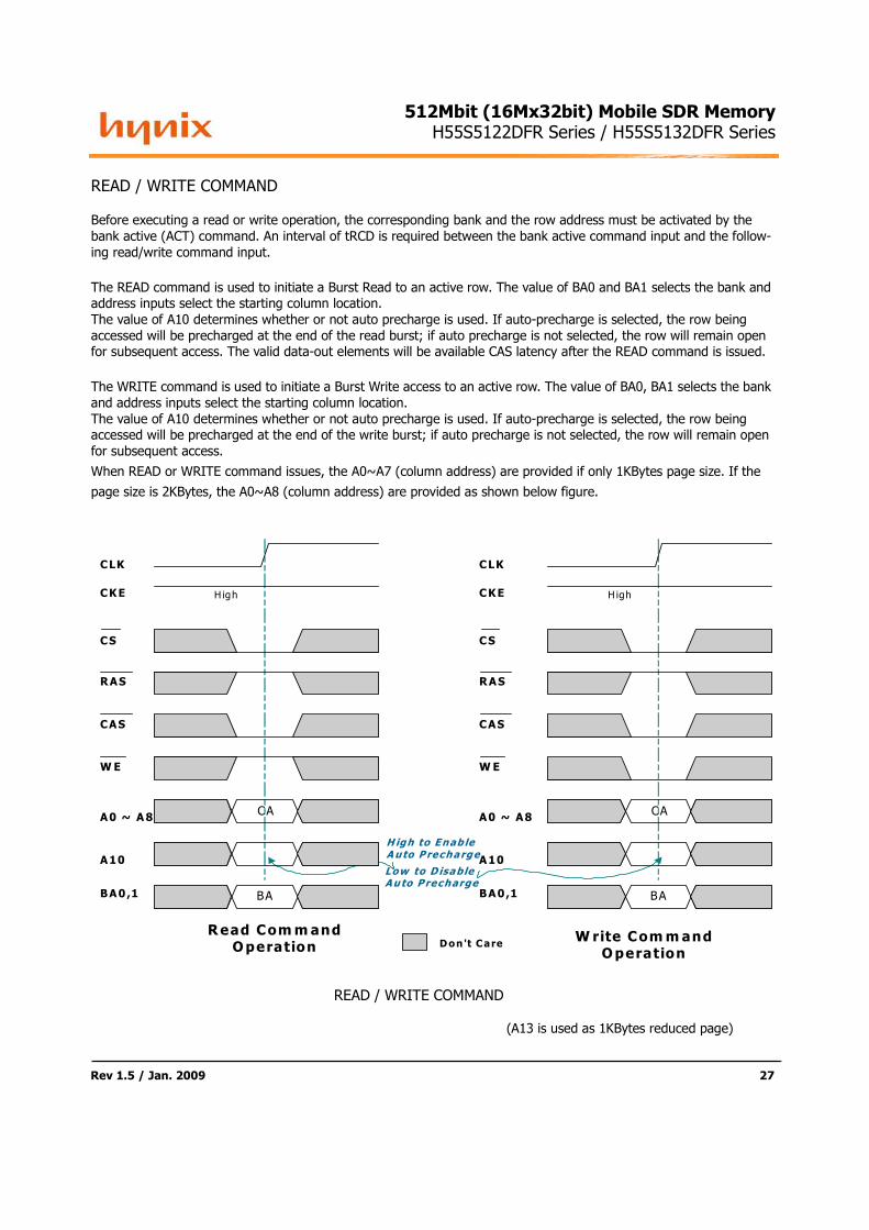
READ / WRITE COMMAND
Before executing a read or write operation, the corresponding bank and the row address must be activated by the
bank active (ACT) command. An interval of tRCD is required between the bank active command input and the follow-
ing read/write command input.
The READ command is used to initiate a Burst Read to an active row. The value of BA0 and BA1 selects the bank and
address inputs select the starting column location.
The value of A10 determines whether or not auto precharge is used. If auto-precharge is selected, the row being
accessed will be precharged at the end of the read burst; if auto precharge is not selected, the row will remain open
for subsequent access. The valid data-out elements will be available CAS latency after the READ command is issued.
The WRITE command is used to initiate a Burst Write access to an active row. The value of BA0, BA1 selects the bank
and address inputs select the starting column location.
The value of A10 determines whether or not auto precharge is used. If auto-precharge is selected, the row being
accessed will be precharged at the end of the write burst; if auto precharge is not selected, the row will remain open
for subsequent access.
When READ or WRITE command issues, the A0~A7 (column address) are provided if only 1KBytes page size. If the
page size is 2KBytes, the A0~A8 (column address) are provided as shown below figure.
READ / WRITE COMMAND
(A13 is used as 1KBytes reduced page)
CS
A0 ~ A8
WE
CAS
RAS
Don't Care
CLK
CKE H igh
CA
BABA0,1
H igh to Enab le Auto P recharge
Low to D isable Auto P recharge
Read Command Operation
W rite Command Operation
A10
CS
A0 ~ A8
WE
CAS
RAS
CLK
CKE H igh
CA
BABA0,1
A10

Rev 1.5 / Jan. 2009 28
11512Mbit (16Mx32bit) Mobile SDR Memory
H55S5122DFR Series / H55S5132DFR Series
READA read operation starts when a read command is input. Output buffer becomes Low-Z in the (/CAS Latency - 1)
cycle after read command set. The SDRAM can perform a burst read operation.
The burst length can be set to 1, 2, 4 and 8. The start address for a burst read is specified by the column address and
the bank select address at the read command set cycle. In a read operation, data output starts after the number of
clocks specified by the /CAS Latency. The /CAS Latency can be set to 2 or 3.
When the burst length is 1, 2, 4 and 8 the DOUT buffer automatically becomes High-Z at the next clock after the suc-
cessive burst-length data has been output.
The /CAS latency and burst length must be specified at the mode register.
Read Burst Showing CAS Latency
CLK
tCK
Command
DQ
Undefined
READ
NOP NOP
Do0 Do1 Do2 Do3
tOHtLZ
tAC
CL = 2
READ
NOP NOP NOP
Do0 Do1 Do2 Do3
tOHtLZ
tAC
CL = 3
Command
DQ
Don't Care

Rev 1.5 / Jan. 2009 29
11512Mbit (16Mx32bit) Mobile SDR Memory
H55S5122DFR Series / H55S5132DFR Series
READ to READData from a read burst may be concatenated or truncated by a subsequent READ command. The first data from the
new burst follows either the last element of a completed burst or the last desired element of a longer burst that is
being truncated.
When another read command is executed at the same ROW address of the same bank as the preceding read com-
mand execution, the second read can be performed after an interval of no less than 1 clock. Even when the first com-
mand is a burst read that is not yet finished, the data read by the second command will be valid.
Consecutive Read Bursts
A READ command can be initiated on any clock cycle following a previous READ command. Non-consecutive Reads are
shown in Figure. Full-speed random read accesses within a page or pages can be performed as shown in Fig.
CLK
Doa0
READ
CL =3
CL =2
Don't Care
Command
Address
DQ
DQ
Doa1 Dob0 Dob1
Doa0 Doa1 Dob0
READ’
BA, Col b
BA, Col a
NOP NOP

Rev 1.5 / Jan. 2009 30
11512Mbit (16Mx32bit) Mobile SDR Memory
H55S5122DFR Series / H55S5132DFR Series
Non-Consecutive Read Bursts
Random Read Bursts
CLK
Don
Don
READ READ
BA, Col n
CL =3
CL =2
Don't Care
1) Don (or b): Data out from column n2) BA, Col n (b) = Bank A, Column n (b)3) Burst Length = 4 : 3 subseqnent elements of Data Out appear in the programmed order following Do n (b)
Command
Address
DQ
DQ
BA, Col b
Dob
Dob
Dog
CLK
CL =3
CL =2
Don't Care
DQ
DQ
READ READ READ READCommand
BA, Col n
Address BA, Col b
BA, Col x
BA, Col g
Don DobDon' Dox Dox' Dob' Dog Dog'
Dox'Don Don' Dox Dob Dob' Dog’
1) Don, etc: Data out from column n, etc n', x', etc : Data Out elements, accoding to the programmd burst order2) BA, Col n = Bank A, Column n3) Burst Length = 1, 2, 4, 8 or full page in cases shown4) Read are to active row in any banks

Rev 1.5 / Jan. 2009 31
11512Mbit (16Mx32bit) Mobile SDR Memory
H55S5122DFR Series / H55S5132DFR Series
READ BURST TERMINATE
Data from any READ burst may be truncated with a BURST TERMINATE command. The BURST TERMINATE latency is
equal to the read (CAS) latency, i.e., the BURST TERMINATE command should be issued X cycles after the READ com-
mand where X equals the desired data-out element.
Terminating a Read Burst
CLK
CL =3
CL =2
Don't Care
DQ
DQ
READ BURSTCommand
BA, Col n
Address
Don Don'
Don Don'
1) Don : Data out from column n2) BA, Col n = Bank A, Column n3) Cases shown are bursts of 4, 8, or full page terminated after 2 data elements

Rev 1.5 / Jan. 2009 32
11512Mbit (16Mx32bit) Mobile SDR Memory
H55S5122DFR Series / H55S5132DFR Series
READ to WRITE
Data from READ burst must be completed or truncated before a subsequent WRITE command can be issued. If trun-
cation is necessary, the BURST TERMINATE command must be used, as shown in next fig.
Read to Write
Notes:
1. Same bank, same ROW address: When the write command is executed at the same ROW address of the same bank as
the preceding read command, the write command can be performed after an interval of no less than 1 clock.
However, DQM must be set High so that the output buffer becomes High-Z before data input.
2. Same bank, different ROW address: When the ROW address changes, consecutive write commands cannot be executed;
it is necessary to separate the two commands with a precharge command and a bank active command.
3. Different bank: When the bank changes, the write command can be performed after an interval of no less than 1 cycle, provided
that the other bank is in the bank active state. However, DQM must be set High so that the output buffer becomes High-Z before
data input.
CLK
CL =3
CL =2
Don't Care
DQ
DQ
READ BURST WRITECommand
BA, Col n
Address
Don Don'
Don Don'
BA, Col b
DIb0 D Ib1 DIb2 DIb3
DIb0 DIb1 D Ib2 DIb3
1) DO n = Data Out from column n; DI b = Data In to column b
Rev 1.5 / Jan. 2009 33
11512Mbit (16Mx32bit) Mobile SDR Memory
H55S5122DFR Series / H55S5132DFR Series
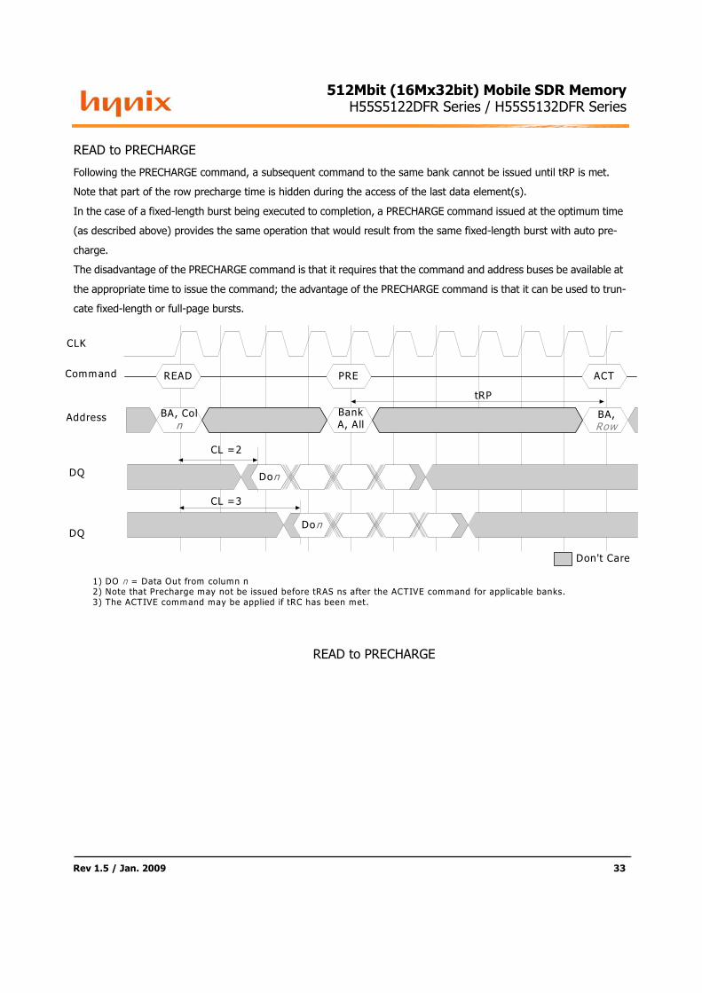
READ to PRECHARGE
Following the PRECHARGE command, a subsequent command to the same bank cannot be issued until tRP is met.
Note that part of the row precharge time is hidden during the access of the last data element(s).
In the case of a fixed-length burst being executed to completion, a PRECHARGE command issued at the optimum time
(as described above) provides the same operation that would result from the same fixed-length burst with auto pre-
charge.
The disadvantage of the PRECHARGE command is that it requires that the command and address buses be available at
the appropriate time to issue the command; the advantage of the PRECHARGE command is that it can be used to trun-
cate fixed-length or full-page bursts.
READ to PRECHARGE
CLK
CL =3
CL =2
Don't Care
DQ
DQ
READ PRE ACTCommand
BA, Col n
AddressBank A, All
BA,Row
Don
tRP
Don
1) DO n = Data Out from column n2) Note that Precharge may not be issued before tRAS ns after the ACTIVE command for applicable banks.3) The ACTIVE command may be applied if tRC has been met.

Rev 1.5 / Jan. 2009 34
11512Mbit (16Mx32bit) Mobile SDR Memory
H55S5122DFR Series / H55S5132DFR Series
WriteInput data appearing on the data bus, is written to the memory array subject to the DM input logic level appearing
coincident with the data. If a given DM signal is registered Low, the corresponding data will be written to the memory;
if the DM signal is registered High, the corresponding data inputs will be ignored, and a write will not be executed to
that byte / column location.
During WRITE bursts, the first valid data-in element will be registered coincident with the WRITE command. Subse-
quent data elements will be registered on each successive positive clock edge. Upon completion of a fixed-length
burst, assuming no other commands have been initiated, the DQ will remain High-Z and any additional input data will
be ignored. A full-page burst will continue until terminated.
Data for any WRITE burst may be truncated with a subsequent WRITE command, and data for a fixed-length WRITE
burst may be immediately followed by data for a WRITE command. The new WRITE command can be issued on any
clock following the previous WRITE command, and the data provided coincident with the new command applies to the
new command.
Basic Write timing parameters for Write Burst Operation
Notes:
1. Same bank, same ROW address: When another write command is executed at the same ROW address of the same bank as the
preceding write command, the second write can be performed after an interval of no less than 1 clock. In the case of burst writes,
the second write command has priority.
2. Same bank, different ROW address: When the ROW address changes, consecutive write commands cannot be executed;
it is necessary to separate the two write commands with a precharge command and a bank active command.
3. Different bank: When the bank changes, the second write can be performed after an interval of no less than 1 clock,
provided that the other bank is in the bank active state. In the case of burst write, the second write command has priority.
CLK
Don't Care
DQ
WRITECommand
BA, Col b
Address
DIb0
DQ DIb0 DIb1
DQ DIb0 DIb1 DIb2 DIb3
DQ DIb0 DIb1 DIb2 DIb3 DIb4 DIb6 DIb7
CL = 2 or 3
BL = 1
BL = 2
BL = 4
BL = 8DIb5

Rev 1.5 / Jan. 2009 35
11512Mbit (16Mx32bit) Mobile SDR Memory
H55S5122DFR Series / H55S5132DFR Series
WRITE to WRITE
Data for any WRITE burst may be concatenated with or truncated with a subsequent WRITE command. In either case,
a continuous flow of input data, can be maintained. The new WRITE command can be issued on any positive edge of
the clock following the previous WRITE command. The first data-in element from the new burst is applied after either
the last element of a completed burst or the last desired data element of a longer burst which is being truncated. The
new WRITE command should be issued X cycles after the first WRITE command, where X equals the number of
desired data-in element.
Concatenated Write Bursts
Random Write Cycles
CLK
Don't Care
WRITE WRITECommand
BA, Col b
Address
DQ DIb0 DIb1 DIb2 DIb3 DIn0 DIn2 DIn3
CL = 2 or 3
DIn1
BA, Col n
DM
CLK
Don't Care
WRITE WRITE WRITE WRITE WRITE NOPCommand
BA, Col b
Address
DQ DIb DIb' DIx DIx’ D In DIa
CL = 2 or 3
DIn’
BA, Col n
BA, Col x
BA, Col a
BA, Col g
D Ia’ DIg DIg’
DM

Rev 1.5 / Jan. 2009 36
11512Mbit (16Mx32bit) Mobile SDR Memory
H55S5122DFR Series / H55S5132DFR Series
WRITE to READ
The preceding burst write operation can be aborted and a new burst read operation can be started by inputting a new
read command in the write cycle. The data of the read command (READ) is output after the lapse of the /CAS latency.
The preceding write operation (WRIT) writes only the data input before the read command.
The data bus must go into a high-impedance state at least one cycle before output of the latest data.
Notes:
1. Same bank, same ROW address: When the read command is executed at the same ROW address of the same bank
as the preceding write command, the read command can be performed after an interval of no less than 1 clock.
However, in the case of a burst write, data will continue to be written until one clock before the read command is
executed.
2. Same bank, different ROW address: When the ROW address changes, consecutive read commands cannot be
executed; it is necessary to separate the two commands with a precharge command and a bank active command.
3. Different bank: When the bank changes, the read command can be performed after an interval of no less than 1
clock, provided that the other bank is in the bank active state. However, in the case of a burst write, data will
continue to be written until one clock before the read command is executed (as in the case of the same bank
and the same address).
CLK
Don't Care
DQ
WRITE READCommand
BA, Col b
Address
DQ
DIb0 DIb1 DOn0 DOn2 DOn3BL = 4
DOn1
DIb0 DIb1 BL = 4CL = 3
BA, Col n
CL = 2
DOn0 DOn2 DOn3DOn1

Rev 1.5 / Jan. 2009 37
11512Mbit (16Mx32bit) Mobile SDR Memory
H55S5122DFR Series / H55S5132DFR Series
WRITE to PRECHARGE
Data for any WRITE burst may be followed by a subsequent PRECHARGE command to the same bank (provided Auto
Precharge was not activated). When the precharge command is executed for the same bank as the write command
that preceded it, the minimum interval between the two commands is 1 clock. However, if the burst write operation is
unfinished, the input data must be masked by means of DQM for assurance of the clock defined by tDPL. To follow a
WRITE without truncating the WRITE burst, tDPL should be met as shown in Fig.
Non-Interrupting Write to Precharge
Data for any WRITE burst may be truncated by a subsequent PRECHARGE command as shown in Figure.
Note that only data-in that are registered prior to the tDPL period are written to the internal array, and any subsequent
data-in should be masked with DM, as shown in next Fig. Following the PRECHARGE command, a subsequent com-
mand to the same bank cannot be issued until tRP is met.
Interrupting Write to Precharge
CLK
WRITE PRECommand
BA, Col b
Address
DQ DIb0 DIOb2BL = 4
DIb1CL = 2 or 3
tDPL
DIb3
CLK
DQ
WRITE PRECommand
BA, Col b
Address
DIb0 DIOb2BL = 4
DIb1CL = 2 or 3
tDPL

Rev 1.5 / Jan. 2009 38
11512Mbit (16Mx32bit) Mobile SDR Memory
H55S5122DFR Series / H55S5132DFR Series
WRITE BURST TERMINATE
WRITE bursts can be truncated with the BURST TERMINATE command. When truncating a WRITE burst, the input
data applied coincident with the BURST TERMINATE command will be ignored. The last data written (provided that
DQM is LOW at that time) will be the input data applied one clock previous to the BURST TERMINATE command.
Terminating a Burst Write command with BST
CLK
DQ
WRITE BSTCommand
BA, Col b
Address
BL = 4 or higher CL = 2 or 3High-Z
Don’t care - Data ignored
DIb0 DIOb2DIb1

Rev 1.5 / Jan. 2009 39
11512Mbit (16Mx32bit) Mobile SDR Memory
H55S5122DFR Series / H55S5132DFR Series
BURST TERMINATEThe BURST TERMINATE command is used to truncate read bursts or write bursts (with auto precharge disabled). The
most recently registered READ or WRITE command prior to the BURST TERMINATE command will be truncated, as
shown in the Operation section of this datasheet. The BURST TERMINATE command is not bank specific.
The below figure shows in case of 1KByte page size. If the page size is 2KByte, A0~A12 are provided.
BURST TERMINATE COMMAND
(A13 is used as 1KBytes reduced page)
CS
A0~A13
WE
CAS
RAS
Don't Care
CLK
CKE High
BA0, 1

Rev 1.5 / Jan. 2009 40
11512Mbit (16Mx32bit) Mobile SDR Memory
H55S5122DFR Series / H55S5132DFR Series
PRECHARGEThe PRECHARGE command is used to deactivate the open row in a particular bank or the open row in all banks.
Another command to the same bank (or banks) being precharged must not be issued until the precharge time (tRP) is
completed.
If one bank is to be precharged, the particular bank address needs to be specified. If all banks are to be precharged,
A10 should be set high along with the PRECHARGE command. If A10 is high, BA0 and BA1 are ignored. A PRECHARGE
command will be treated as a NOP if there is no open row in that bank, or if the previously open row is already in the
process of precharging.
The below figure shows in case of 1KByte page size. If the page size is 2KByte, A0~A12 are provided.
PRECHARGE command
(A13 is used as 1KBytes reduced page)
AUTO PRECHARGEAuto Precharge is a feature which performs the same individual bank precharge function as described above, but with-
out requiring an explicit command.
This is accomplished by using A10 (A10=high), to enable auto precharge in conjunction with a specific Read or Write
command. This precharges the bank/row after the Read or Write burst is complete.
Auto precharge is non persistent, so it should be enabled with a Read or Write command each time auto precharge is
desired. Auto precharge ensures that a precharge is initiated at the earliest valid stage within a burst.
The user must not issue another command to the same bank until the precharge time (tRP) is completed.
Don't Care
CS
A0~A9A11~A13
WE
CAS
RAS
CKE High
BABA0,1
A10
Bank Address
A10 defines the prechargemode when a prechargecommand, a read commandor a write command isissued.
If A10 = High when aprecharge command isissued, all banks areprecharged.
If A10 = Low when aprecharge command isissued, only the bank that isselected by BA1/BA0 isprecharged.
If A10 = High when read orwrite command, auto-precharge function isenabled.While A10 = Low, auto-precharge function isdisabled.

Rev 1.5 / Jan. 2009 41
11512Mbit (16Mx32bit) Mobile SDR Memory
H55S5122DFR Series / H55S5132DFR Series
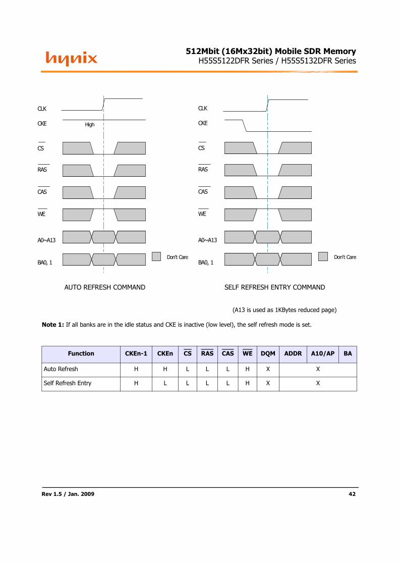
AUTO REFRESH AND SELF REFRESHMobile SDRAM devices require a refresh of all rows in any rolling 64ms interval. Each refresh is generated in one of two
ways: by an explicit AUTO REFRESH command, or by an internally timed event in SELF REFRESH mode:
- AUTO REFRESH.
This command is used during normal operation of the Mobile SDRAM. It is non persistent, so must be issued each time
a refresh is required. The refresh addressing is generated by the internal refresh controller.The Mobile SDRAM requires
AUTO REFRESH commands at an average periodic interval of tREF.
To allow for improved efficiency in scheduling and switching between tasks, some flexibility in the absolute refresh
interval is provided. A maximum of eight AUTO REFRESH commands can be posted to any given Mobile SDRMA, and
the maximum absolute interval between any AUTO REFRESH command and the next AUTO REFRESH command is
8*tREF.
-SELF REFRESH.
This state retains data in the Mobile SDRAM, even if the rest of the system is powered down. Note refresh interval tim-
ing while in Self Refresh mode is scheduled internally in the Mobile SDRAM and may vary and may not meet tREF time.
After executing a self-refresh command, the self-refresh operation continues while CKE is held Low. During self refresh
operation, all ROW addresses are refreshed by the internal refresh timer. A self-refresh is terminated by a self-refresh
exit command. Before and after self-refresh mode, execute auto-refresh to all refresh addresses in or within tREF
(max.) period on the condition 1 and 2 below.
1. Enter self-refresh mode within time as below* after either burst refresh or distributed refresh at equal interval to all
refresh addresses are completed.
2. Start burst refresh or distributed refresh at equal interval to all refresh addresses within time as below* after exiting
from self-refresh mode.
Note: tREF (max.) / refresh cycles.
The use of SELF REFRESH mode introduces the possibility that an internally timed event can be missed when CKE is
raised for exit from self refresh mode. Upon exit from SELF REFRESH an extra AUTO REFRESH command is recom-
mended. In the self refresh mode, two additional power-saving options exist. They are Temperature Compensated Self
Refresh and Partial Array Self Refresh and are described in the Extended Mode Register section.
The Self Refresh command is used to retain cell data in the Mobile SDRAM. In the Self Refresh mode, the Mobile
SDRAM operates refresh cycle asynchronously.
The Self Refresh command is initiated like an Auto Refresh command except CKE is disabled(Low). The Mobile SDRAM
can accomplish an special Self Refresh operation by the specific modes(PASR) programmed in extended mode regis-
ters. The Mobile SDRAM can control the refresh rate automatically by the temperature value of Auto TCSR(Tempera-
ture Compensated Self Refresh) to reduce self refresh current and select the memory array to be refreshed by the
value of PASR(Partial Array Self Refresh). The Mobile SDRAM can reduce the self refresh current(IDD6) by using these
two modes.
The figure of next page shows in case of 1KByte page size. If the page size is 2KByte, A0~A12 are provided.
Rev 1.5 / Jan. 2009 42
11512Mbit (16Mx32bit) Mobile SDR Memory
H55S5122DFR Series / H55S5132DFR Series
AUTO REFRESH COMMAND SELF REFRESH ENTRY COMMAND
(A13 is used as 1KBytes reduced page)
Note 1: If all banks are in the idle status and CKE is inactive (low level), the self refresh mode is set.
Function CKEn-1 CKEn CS RAS CAS WE DQM ADDR A10/AP BA
Auto Refresh H H L L L H X X
Self Refresh Entry H L L L L H X X
CS
A0~A13
WE
CAS
RAS
Don't Care
CLK
CKE
BA0, 1
CS
A0~A13
WE
CAS
RAS
Don't Care
CLK
CKE High
BA0, 1

Rev 1.5 / Jan. 2009 43
11512Mbit (16Mx32bit) Mobile SDR Memory
H55S5122DFR Series / H55S5132DFR Series
MODE REGISTER SETThe mode registers are loaded via the address bits.
BA0 and BA1 are used to select between the Mode Register and the Extended Mode Register. See the Mode Register
description in the register definition section. The MODE REGISTER SET command can only be issued when all banks
are idle and no bursts are in progress, and a subsequent executable command cannot be issued until tMRD is met.
The below figure shows in case of 1KByte page size. If the page size is 2KByte, A0~A12 are provided.
(A13 is used as 1KBytes reduced page)
MODE REGISTER SET COMMANDNote: BA0=BA1=Low loads the Mode Register, whereas BA0=Low and BA1=High loads the Extended Mode Register.
Code = Mode Register / Extended Mode Register selection
(BA0, BA1) and op-code (A0 - An)
tMRD DEFINITION
MRS NOP Valid
Code Valid
tMRD
CLK
Command
Address
Don't Care
CS
A0~A13
WE
CAS
RAS
Don't Care
CLK
CKE
BA0, 1
Code
Code
High

Rev 1.5 / Jan. 2009 44
11512Mbit (16Mx32bit) Mobile SDR Memory
H55S5122DFR Series / H55S5132DFR Series
POWER DOWNPower down occurs if CKE is set low coincident with Device Deselect or NOP command and when no accesses are in
progress. If power down occurs when all banks are idle, it is Precharge Power Down.
If Power down occurs when one or more banks are Active, it is referred to as Active power down. The device cannot
stay in this mode for longer than the refresh requirements of the device, without losing data. The power down state is
exited by setting CKE high while issuing a Device Deselect or NOP command.
If power-down occurs when all banks are idle, this mode is referred to as precharge power-down; if power-down
occurs when there is a row active in any bank, this mode is referred to as active power-down. Entering power-down
deactivates the input and output buffers, excluding CKE, for maximum power savings while in standby.
DEEP POWER-DOWNThe Deep Power-Down (DPD) mode enables very low standby currents. All internal voltage generators inside the
Mobile SDRAM are stopped and all memory data is lost in this mode.
All the information in the Mode Register and the Extended Mode Register is lost. Next Figure, DEEP POWER-DOWN COMMAND shows the DEEP POWER-DOWN command All banks must be in idle state with no activity on the data bus
prior to entering the DPD mode. While in this state, CKE must be held in a constant low state.
To exit the DPD mode, CKE is taken high after the clock is stable and NOP command must be maintained for at least
200 us. After 200 us a complete re-initialization routing is required defined for the initialization sequence.
The below figure shows in case of 1KByte page size. If the page size is 2KByte, A0~A12 are provided.
(A13 is used as 1KBytes reduced page)
CS
A0~A13
WE
CAS
RAS
Don't Care
CLK
CKE
BA0, 1
POWER-DOWN COMMAND
CS
A0~A13
WE
CAS
RAS
Don't Care
CLK
CKE
BA0, 1
DEEP POWER-DOWN COMMAND

Rev 1.5 / Jan. 2009 45
11512Mbit (16Mx32bit) Mobile SDR Memory
H55S5122DFR Series / H55S5132DFR Series
CLK
CKE
COMMAND NOP NOP ACTIVE
Input buffers gated off
tRCD
tRAS
tRCEnter power-down mode. Exit power-down mode.
All banks idle
DON’T CARE
CLK
CKE
COMMAND
Pre-charge all Deep Power down entry
DON’T CARE
NOP APCGNOPNOPPCG
Input buffers gated off 200us(min)
tCKS tCKS
Deep Power down Exit

Rev 1.5 / Jan. 2009 46
11512Mbit (16Mx32bit) Mobile SDR Memory
H55S5122DFR Series / H55S5132DFR Series
Qa2Qa1Qa0
Ra
Ra Ca
tCKS tCKS tCKS tCKS
CLK
CKE
CS
RAS
WE
VDDR
BA0, BA1
AP
DQ
DQM
CAS
Precharge Power down
Entry
Precharge Power down
Exit
Row Active
Active Power down
Entry
Active Power down
Exit
Read Precharge
Hi-Z
Don’t care
Note : CKE should be set high at least 1CLK + tCKS prior to Row active command.
Power down Exit Time

Rev 1.5 / Jan. 2009 47
11512Mbit (16Mx32bit) Mobile SDR Memory
H55S5122DFR Series / H55S5132DFR Series
tCKtCH
NOPAUTO
REFRESHAny COM
tCKS tCKH
tCMS tCMH
ALL BANKS
SINGLE BANK
Precharge allactive banks
DON’T CARE
CLK
CKE
COMMAND
DQM
A0-
A9,Amax
A10
BA0, BA1
DQ
PRECHARGE
BANKS
tAS tAH
High-Z
tRP tXSR
tCL
NOPor COMMAND
INHIBIT
Enter self refresh mode Exit self refresh mode
(Restart refresh time base)
tCKS tRAS(MIN)

Rev 1.5 / Jan. 2009 48
11512Mbit (16Mx32bit) Mobile SDR Memory
H55S5122DFR Series / H55S5132DFR Series
Power-up and InitializationLike a Synchronous DRAM, Low Power SDRAM(Mobile SDRAM) must be powered up and initialized in a predefined man-
ner. Power must be applied to VDD and VDDQ(simultaneously). The clock signal must be started at the same time. After
power up, an initial pause of 200 usec is required. And a precharge all command will be issued to the Mobile SDRAM.
Then, 8 or more Auto refresh cycles will be provided. After the Auto refresh cycles are completed, a mode register
set(MRS) command will be issued to program the specific mode of operation (Cas Latency, Burst length, etc.) And a
extended mode register set command will be issued to program specific mode of self refresh operation(PASR). The fol-
lowing these cycles, the Mobile SDRAM is ready for normal operation.
Programming the registers
Mode RegisterThe mode register contains the specific mode of operation of the Mobile SDRAM. This register includes the selection of
a burst length(1, 2, 4, 8, Full Page), a cas latency(2 or 3), a burst type. The mode register set must be done before any
activate command after the power up sequence. Any contents of the mode register be altered by re-programming the
mode register through the execution of mode register set command.
Extended Mode RegisterThe extended mode register contains the specific features of self refresh operation of the Mobile SDRAM. This register
includes the selection of partial arrays to be refreshed(half array, quarter array, etc.). The extended mode register set
must be done before any activate command after the power up sequence. Any contents of the mode register be altered
by re-programming the mode register through the execution of extended mode register set command.
Bank(Row) ActiveThe Bank Active command is used to activate a row in a specified bank of the device. This command is initiated by
activating CS, RAS and deasserting CAS, WE at the positive edge of the clock. The value on the BA1 and BA0 selects
the bank, and the value on the A0-A13(or A12 which depends on page size) selects the row. This row remains active
for column access until a precharge command is issued to that bank. Read and write operations can only be initiated
on this activated bank after the minimum tRCD time is passed from the activate command.
ReadThe READ command is used to initiate the burst read of data. This command is initiated by activating CS, CAS, and
deasserting WE, RAS at the positive edge of the clock. BA1 and BA0 inputs select the bank, A8-A0 address inputs select
the starting column location. The value on input A10 determines whether or not Auto Precharge is used. If Auto Pre-
charge is selected the row being accessed will be precharged at the end of the READ burst; if Auto Precharge is not
selected, the row will remain active for subsequent accesses.
The length of burst and the CAS latency will be determined by the values programmed during the MRS command.
WriteThe WRITE command is used to initiate the burst write of data. This command is initiated by activating CS, CAS, WE
and deasserting RAS at the positive edge of the clock. BA1 and BA0 inputs select the bank, A8-A0 address inputs select
the starting column location. The value on input A10 determines whether or not Auto Precharge is used.
If Auto Precharge is selected the row being accessed will be precharged at the end of the WRITE burst; if Auto Pre-
charge is not selected, the row will remain active for subsequent accesses.
Rev 1.5 / Jan. 2009 49
11512Mbit (16Mx32bit) Mobile SDR Memory
H55S5122DFR Series / H55S5132DFR Series
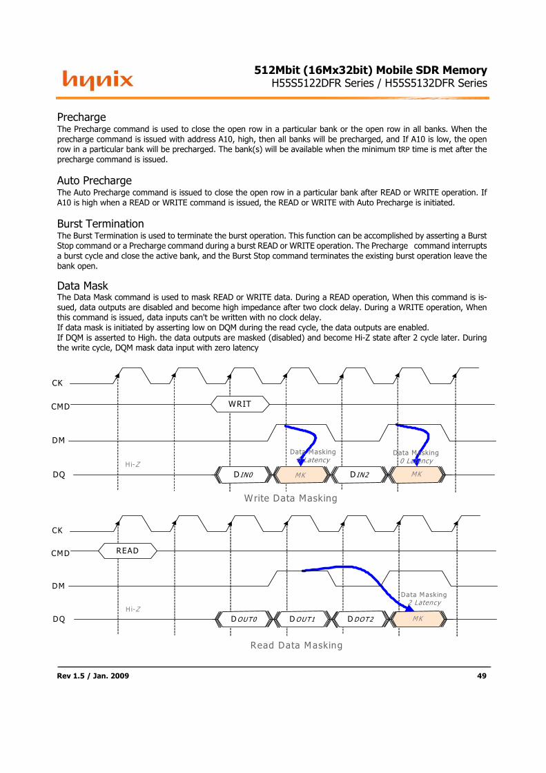
PrechargeThe Precharge command is used to close the open row in a particular bank or the open row in all banks. When the
precharge command is issued with address A10, high, then all banks will be precharged, and If A10 is low, the open
row in a particular bank will be precharged. The bank(s) will be available when the minimum tRP time is met after the
precharge command is issued.
Auto PrechargeThe Auto Precharge command is issued to close the open row in a particular bank after READ or WRITE operation. If
A10 is high when a READ or WRITE command is issued, the READ or WRITE with Auto Precharge is initiated.
Burst TerminationThe Burst Termination is used to terminate the burst operation. This function can be accomplished by asserting a Burst
Stop command or a Precharge command during a burst READ or WRITE operation. The Precharge command interrupts
a burst cycle and close the active bank, and the Burst Stop command terminates the existing burst operation leave the
bank open.
Data Mask The Data Mask command is used to mask READ or WRITE data. During a READ operation, When this command is is-
sued, data outputs are disabled and become high impedance after two clock delay. During a WRITE operation, When
this command is issued, data inputs can't be written with no clock delay.
If data mask is initiated by asserting low on DQM during the read cycle, the data outputs are enabled.
If DQM is asserted to High. the data outputs are masked (disabled) and become Hi-Z state after 2 cycle later. During
the write cycle, DQM mask data input with zero latency
DM
CMD
CK
D0 D1DQ
Data Masking0 Latency
Hi-Z
D IN0 D0 D1 D0 D1DIN2 D0 D1
WRIT
MK MK
Data Masking0 Latency
Write Data Masking
DM
CMD
CK
D0 D1DQ
Data Masking2 Latency
Hi-Z
DOUT0 D0 D1DOUT1 D0 D1DDOT2 D0 D1
READ
MK
Read Data Masking

Rev 1.5 / Jan. 2009 50
11512Mbit (16Mx32bit) Mobile SDR Memory
H55S5122DFR Series / H55S5132DFR Series
Clock Suspend
The Clock Suspend command is used to suspend the internal clock of Mobile SDRAM. The clock suspend operation stops
transmission of the clock to the internal circuits of the device during burst transfer of data to stop the operation of the
device. During normal access mode, CKE is keeping High. When CKE is low, it freezes the internal clock and extends
data Read and Write operations. (See examples in next Figures)
CLK
CKE
Q1 Q2 Q3 Q4
RD
Internal CLK
Clock SuspendMode
WR
D1 D2 D3 D4
Clock SuspendMode
DQ
Command
CKE
Command
Internal CLK
DQ
Frozen Int. CLK by CKE(CKE = Fixed Low)
Masked by CKE
Masked by CKE
Frozen Int. CLK by CKE(CKE = Fixed Low)

Rev 1.5 / Jan. 2009 51
11512Mbit (16Mx32bit) Mobile SDR Memory
H55S5122DFR Series / H55S5132DFR Series
Power Down
The Power Down command is used to reduce stand-by current. Before this command is issued, all banks must be pre-
charged and tRP must be passed after a precharge command. Once the Power Down command is initiated by keeping
CKE low, all of the input buffer except CKE are gated off.
Auto Refresh
The Auto Refresh command is used during normal operation and is similar to CBR refresh in Conventional DRAMs.
This command must be issued each time a refresh is required. When an Auto Refresh command is issued, the address
bits is ''Don't care'', because the specific address bits is generated by internal refresh address counter.
Self Refresh
The Self Refresh command is used to retain cell data in the Mobile SDRAM. In the Self Refresh mode, the Mobile SDRAM
operates refresh cycle asynchronously.
The Self Refresh command is initiated like an Auto Refresh command except CKE is disabled(Low). The Mobile SDRAM
can accomplish an special Self Refresh operation by the specific modes(PASR) programmed in extended mode registers.
The Mobile SDRAM can control the refresh rate automatically by the temperature value of Auto TCSR(Temperature
Compensated Self Refresh) to reduce self refresh current and select the memory array to be refreshed by the value of
PASR(Partial Array Self Refresh). The Mobile SDRAM can reduce the self refresh current(IDD6) by using these two
modes.
Deep Power Down
The Deep Power Down Mode is used to achieve maximum power reduction by cutting the power of the whole memory
array of the devices.
For more information, see the special operation for Low Power consumption of this data sheet.
Rev 1.5 / Jan. 2009 52
11512Mbit (16Mx32bit) Mobile SDR Memory
H55S5122DFR Series / H55S5132DFR Series
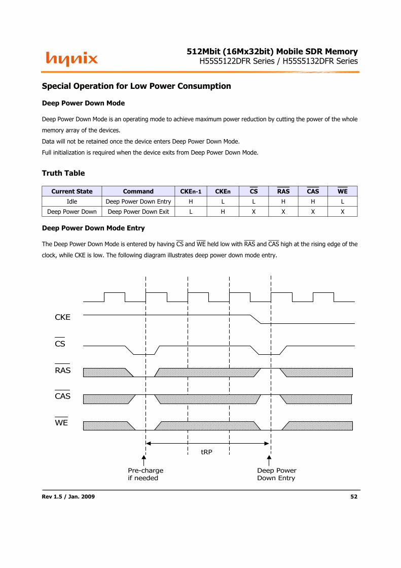
Special Operation for Low Power Consumption
Deep Power Down Mode
Deep Power Down Mode is an operating mode to achieve maximum power reduction by cutting the power of the whole
memory array of the devices.
Data will not be retained once the device enters Deep Power Down Mode.
Full initialization is required when the device exits from Deep Power Down Mode.
Truth Table
Deep Power Down Mode Entry
The Deep Power Down Mode is entered by having CS and WE held low with RAS and CAS high at the rising edge of the
clock, while CKE is low. The following diagram illustrates deep power down mode entry.
Current State Command CKEn-1 CKEn CS RAS CAS WE
Idle Deep Power Down Entry H L L H H L
Deep Power Down Deep Power Down Exit L H X X X X
CKE
CS
RAS
CAS
WE
Pre-chargeif needed
tRP
Deep PowerDown Entry
Rev 1.5 / Jan. 2009 53
11512Mbit (16Mx32bit) Mobile SDR Memory
H55S5122DFR Series / H55S5132DFR Series
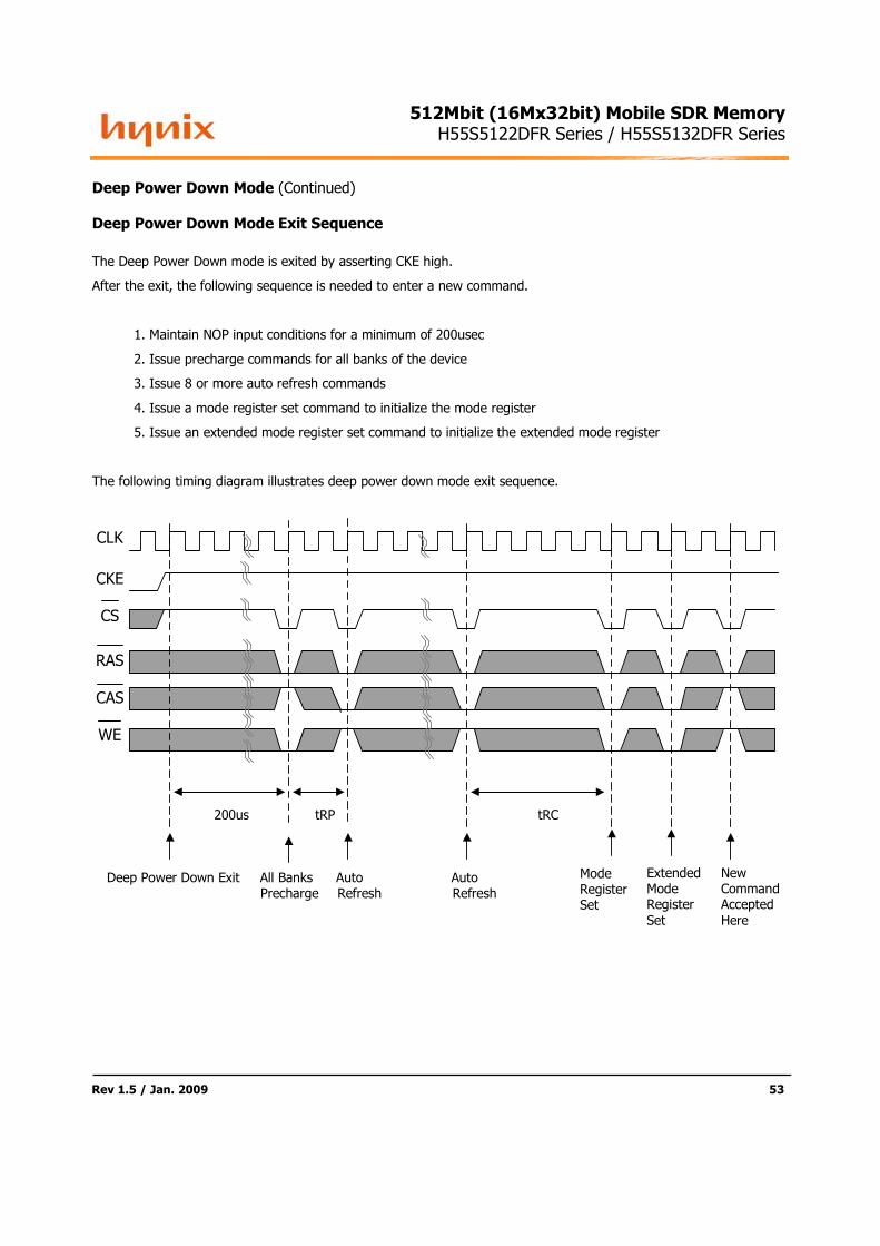
Deep Power Down Mode (Continued)
Deep Power Down Mode Exit Sequence
The Deep Power Down mode is exited by asserting CKE high.
After the exit, the following sequence is needed to enter a new command.
1. Maintain NOP input conditions for a minimum of 200usec
2. Issue precharge commands for all banks of the device
3. Issue 8 or more auto refresh commands
4. Issue a mode register set command to initialize the mode register
5. Issue an extended mode register set command to initialize the extended mode register
The following timing diagram illustrates deep power down mode exit sequence.
CKE
CLK
CS
RAS
CAS
WE
200us tRP tRC
Deep Power Down Exit All BanksPrecharge
AutoRefresh
AutoRefresh
ModeRegisterSet
ExtendedModeRegister
Set
NewCommandAccepted
Here

Rev 1.5 / Jan. 2009 54
11512Mbit (16Mx32bit) Mobile SDR Memory
H55S5122DFR Series / H55S5132DFR Series
PACKAGE INFORMATION
90 Ball FBGA 0.8mm pitch (8.0mm x 13.0mm)
Unit [mm]0.8
0.35+/- 0.05
0.80 Typ.
1.00 max
0.45+/- 0.05
A1 INDEX MARK
13.0
Typ.
BottomView
0.90
11.2
Typ.
6.40 Typ.
8.00 Typ.0.8Typ.
0.8
0.90.


![Untitled Document [docs-europe.electrocomponents.com]docs-europe.electrocomponents.com/webdocs/0920/0900766b809201d… · Schneider Electric Brands ZELIO-CONTROL Measurement Relays](https://static.fdocuments.in/doc/165x107/5abeae277f8b9a5d718d478e/untitled-document-docs-docs-schneider-electric-brands-zelio-control-measurement.jpg)


