SPECIFICATION FOR APPROVAL Title - Provider of LCD ... · PDF fileProduct Specification 1/ 31...
31
Product Specification 1 / 31 LP156WH2 Liquid Crystal Display Ver. 1.0 Mar. 02, 2010 SPECIFICATION FOR APPROVAL 15.6” HD TFT LCD Title MODEL Customer *When you obtain standard approval, please use the above model name without suffix LP156WH2 *MODEL TLQB Suffix LG Display Co., Ltd. SUPPLIER ) ) ( ( Final Specification Preliminary Specification Please return 1 copy for your confirmation with your signature and comments. / / / SIGNATURE APPROVED BY Products Engineering Dept. LG Display Co., Ltd PREPARED BY REVIEWED BY SIGNATURE APPROVED BY S. R. Kim / Manager PREPARED BY REVIEWED BY SIGNATURE APPROVED BY Hans Kim / S.Manager J. P. Lee / Engineer B. I. Park / Engineer
Transcript of SPECIFICATION FOR APPROVAL Title - Provider of LCD ... · PDF fileProduct Specification 1/ 31...
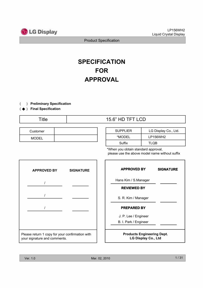
Product Specification
1 / 31
LP156WH2Liquid Crystal Display
Ver. 1.0 Mar. 02, 2010
SPECIFICATIONFOR
APPROVAL
15.6” HD TFT LCDTitle
MODEL
Customer
*When you obtain standard approval,please use the above model name without suffix
LP156WH2*MODEL
TLQBSuffix
LG Display Co., Ltd.SUPPLIER
))
((
Final SpecificationPreliminary Specification
Please return 1 copy for your confirmation withyour signature and comments.
/
/
/
SIGNATUREAPPROVED BY
Products Engineering Dept.LG Display Co., Ltd
PREPARED BY
REVIEWED BY
SIGNATUREAPPROVED BY
S. R. Kim / Manager
PREPARED BY
REVIEWED BY
SIGNATUREAPPROVED BY
Hans Kim / S.Manager
J. P. Lee / Engineer
B. I. Park / Engineer
Product Specification
2 / 31
LP156WH2Liquid Crystal Display
Ver. 1.0 Mar. 02, 2010
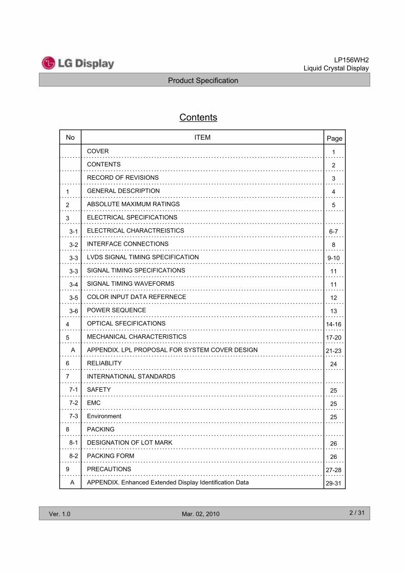
Contents
25EMC7-2
21-23APPENDIX. LPL PROPOSAL FOR SYSTEM COVER DESIGNA
9-10LVDS SIGNAL TIMING SPECIFICATION3-3
29-31APPENDIX. Enhanced Extended Display Identification Data A
27-28PRECAUTIONS9
12
8INTERFACE CONNECTIONS3-2
COLOR INPUT DATA REFERNECE3-5
26DESIGNATION OF LOT MARK8-1
26PACKING FORM8-2
PACKING8
25Environment7-3
1COVER
2CONTENTS
3RECORD OF REVISIONS
4GENERAL DESCRIPTION1
5ABSOLUTE MAXIMUM RATINGS2
ELECTRICAL SPECIFICATIONS3
6-7ELECTRICAL CHARACTREISTICS3-1
11SIGNAL TIMING SPECIFICATIONS3-3
11SIGNAL TIMING WAVEFORMS3-4
13POWER SEQUENCE3-6
14-16OPTICAL SFECIFICATIONS4
17-20MECHANICAL CHARACTERISTICS5
24RELIABLITY6
INTERNATIONAL STANDARDS7
25SAFETY7-1
PageITEMNo

Product Specification
3 / 31
LP156WH2Liquid Crystal Display
Ver. 1.0 Mar. 02, 2010
RECORD OF REVISIONS
0.0
EDIDver
First Draft (Final Specification)-Mar. 02, 20100.0
DescriptionPageRevision DateRevision No

Product Specification
4 / 31
LP156WH2Liquid Crystal Display
Ver. 1.0 Mar. 02, 2010
1. General Description
General Features
YesRoHS Compliance
Hard Coating(3H), Glare treatment of the front polarizerSurface Treatment
6-bit, 262,144 colorsColor Depth1366 horiz. By 768 vert. Pixels RGB strip arrangementPixel Format
200 cd/m2(Typ.5 point)Luminance, WhiteTotal 4.7W (Typ.) @ LCM circuit 1.5 W (Typ.), B/L input 3.2 W (Typ.)Power Consumption450g (Max.)WeightTransmissive mode, normally whiteDisplay Operating Mode
Yes for allBFR / PVC / As Free
0.252mm 0.252 mmPixel Pitch359.3(H, typ) 209.5(V, typ) 5.5(D,max) [mm]Outline Dimension15.6 inches diagonal Active Screen Size
The LP156WH2 is a Color Active Matrix Liquid Crystal Display with an integral Light Emitting Diode (LED) backlight system. The matrix employs a-Si Thin Film Transistor as the active element. It is a transmissive type display operating in the normally white mode. This TFT-LCD has 15.6 inches diagonally measured active display area with HD resolution(768 vertical by 1366 horizontal pixel array). Each pixel is divided into Red, Green and Blue sub-pixels or dots which are arranged in vertical stripes. Gray scale or the brightness of the sub-pixel color is determined with a 6-bit gray scale signal for each dot, thus, presenting a palette of more than 262,144 colors. The LP156WH2 has been designed to apply the interface method that enables low power, high speed, low EMI. The LP156WH2 is intended to support applications where thin thickness, low power are critical factors and graphic displays are important. In combination with the vertical arrangement of the sub-pixels, the LP156WH2 characteristics provide an excellent flat display for office automation products such as Notebook PC.
Control & Data Power EDID signal & Power
TFT-LCD Panel
(HD, DRD, TN)
1
Timing Control
(Tcon) Block
Timing Control
(Tcon) Block
User connector
40Pin
EEPROM Blockfor EDID
EEPROM Blockfor EDID
Source Driver(Bottom Bent)
LED Backlight Ass’y
TCLKs
LVDS1port
VCC
LED DriverBlock
LED DriverBlock
FB
Power
Block
Power
Block
DVCC, AVDDVGH, VGL, GMA
Mini-LVDS
GIP CLKs, DSC
VOUT_LED
DVCC
VLED
LED_ENPWM
768
1366
Product Specification
5 / 31
LP156WH2Liquid Crystal Display
Ver. 1.0 Mar. 02, 2010
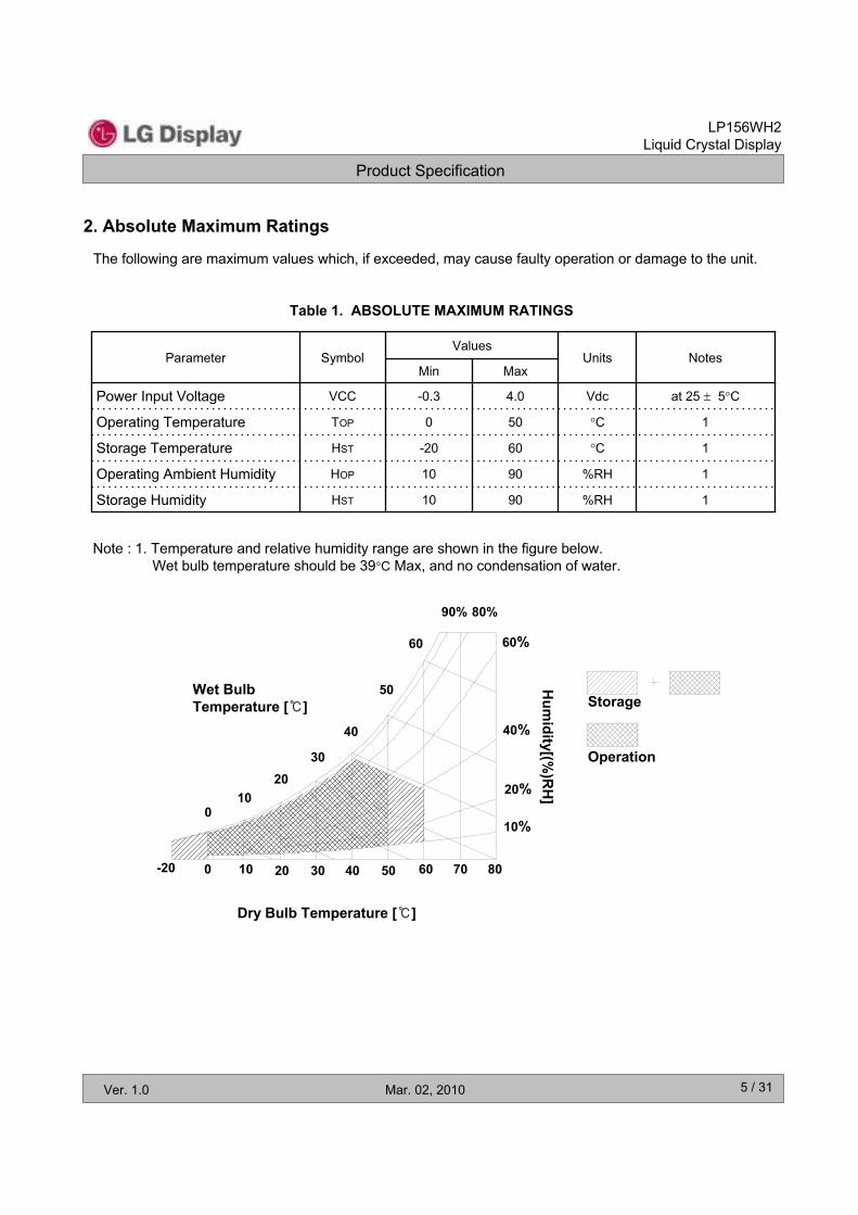
2. Absolute Maximum Ratings
The following are maximum values which, if exceeded, may cause faulty operation or damage to the unit.
Table 1. ABSOLUTE MAXIMUM RATINGS
Storage
Operation
10 20 30 40 50 60 70 800-20
Dry Bulb Temperature [ ]
10%
20%
40%
60%
90% 80%
010
2030
40
50
60
Wet BulbTemperature [ ]
Hum
idity[(%)R
H]
Units
1%RH9010HOPOperating Ambient Humidity
1%RH9010HSTStorage Humidity
1C60-20HSTStorage Temperature
1C500TOPOperating Temperature
at 25 5 CVdc4.0-0.3VCCPower Input Voltage
MaxMinParameter Notes
ValuesSymbol
Note : 1. Temperature and relative humidity range are shown in the figure below. Wet bulb temperature should be 39 C Max, and no condensation of water.
Product Specification
6 / 31
LP156WH2Liquid Crystal Display
Ver. 1.0 Mar. 02, 2010
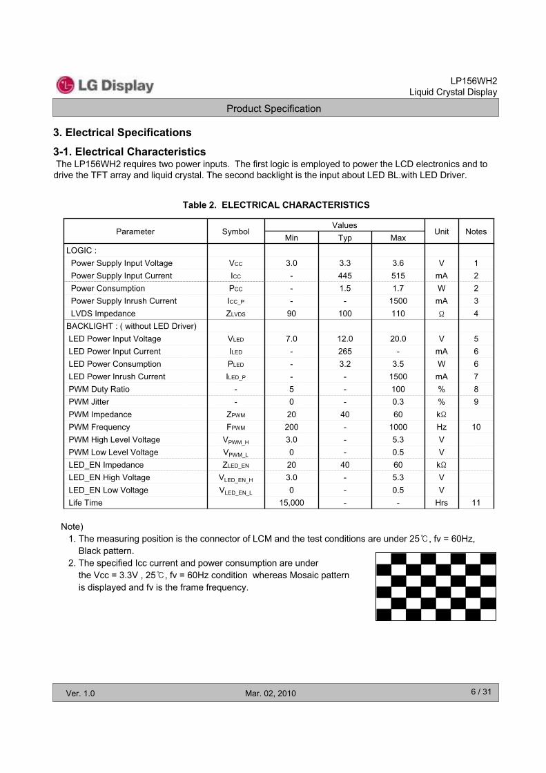
3. Electrical Specifications
3-1. Electrical CharacteristicsThe LP156WH2 requires two power inputs. The first logic is employed to power the LCD electronics and to drive the TFT array and liquid crystal. The second backlight is the input about LED BL.with LED Driver.
Table 2. ELECTRICAL CHARACTERISTICS
V5.3-3.0VLED_EN_HLED_EN High Voltage
9%0.3-0-PWM Jitter
411010090ZLVDSLVDS Impedance
k604020ZPWMPWM Impedance
8%100-5-PWM Duty Ratio7mA1500--ILED_PLED Power Inrush Current6W3.53.2-PLEDLED Power Consumption
V0.5-0VLED_EN_LLED_EN Low Voltage11Hrs--15,000Life Time
k604020ZLED_ENLED_EN Impedance
V5.3-3.0VPWM_HPWM High Level Voltage
6mA-265-ILEDLED Power Input Current5V20.012.07.0VLEDLED Power Input Voltage
3mA1500--ICC_PPower Supply Inrush Current
BACKLIGHT : ( without LED Driver)
V0.5-0VPWM_LPWM Low Level Voltage
10Hz1000-200FPWMPWM Frequency
2mA515445-2W1.71.5-PCCPower Consumption
1V3.63.33.0VCCPower Supply Input VoltageICCPower Supply Input Current
LOGIC :
Parameter SymbolMaxTypMin
NotesUnitValues
Note)1. The measuring position is the connector of LCM and the test conditions are under 25 , fv = 60Hz,
Black pattern. 2. The specified Icc current and power consumption are under
the Vcc = 3.3V , 25 , fv = 60Hz condition whereas Mosaic patternis displayed and fv is the frame frequency.
Product Specification
7 / 31
LP156WH2Liquid Crystal Display
Ver. 1.0 Mar. 02, 2010
3. Electrical Specifications
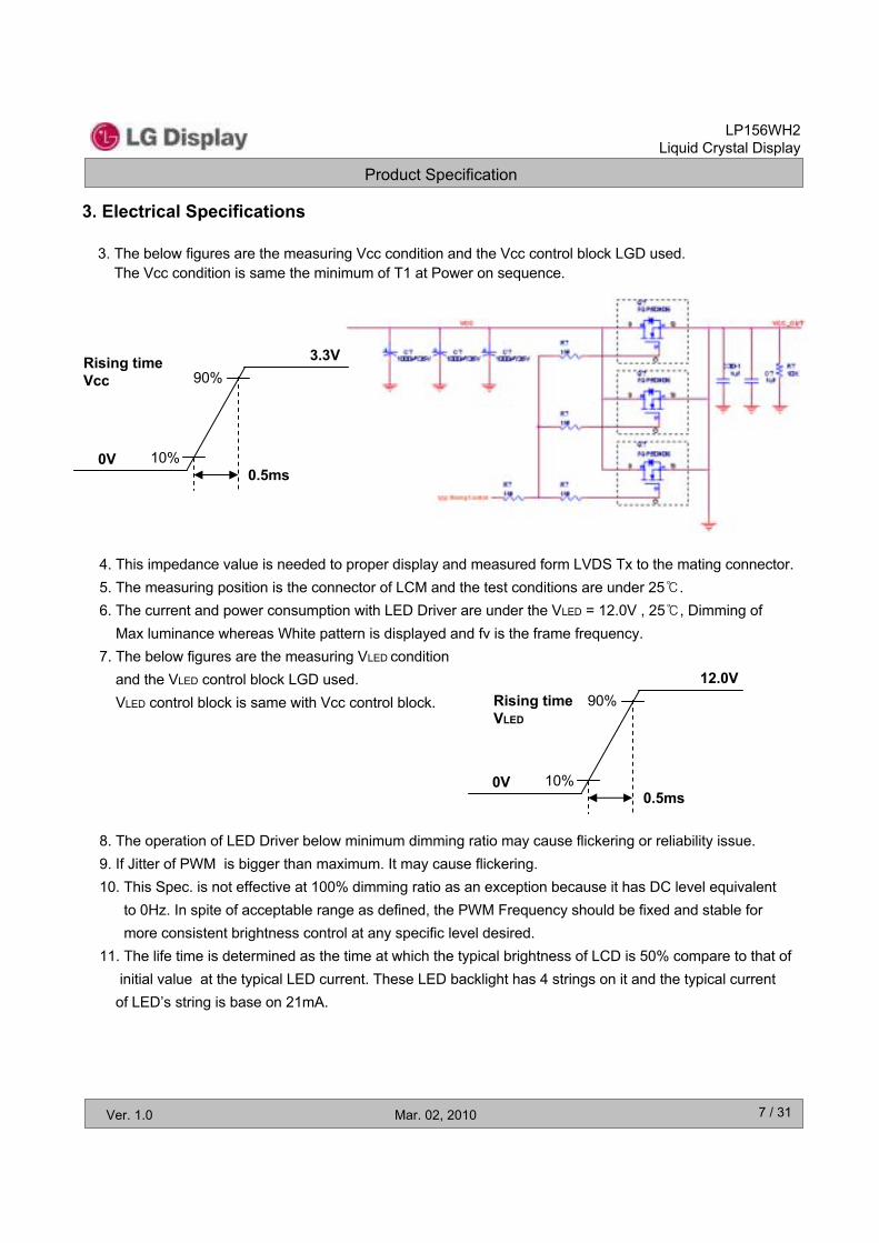
3. The below figures are the measuring Vcc condition and the Vcc control block LGD used.The Vcc condition is same the minimum of T1 at Power on sequence.
10%
90%
0.5ms
3.3V
0V
Rising timeVcc
4. This impedance value is needed to proper display and measured form LVDS Tx to the mating connector.5. The measuring position is the connector of LCM and the test conditions are under 25 .6. The current and power consumption with LED Driver are under the VLED = 12.0V , 25 , Dimming of
Max luminance whereas White pattern is displayed and fv is the frame frequency.7. The below figures are the measuring VLED condition
and the VLED control block LGD used.VLED control block is same with Vcc control block.
8. The operation of LED Driver below minimum dimming ratio may cause flickering or reliability issue.9. If Jitter of PWM is bigger than maximum. It may cause flickering.10. This Spec. is not effective at 100% dimming ratio as an exception because it has DC level equivalent
to 0Hz. In spite of acceptable range as defined, the PWM Frequency should be fixed and stable for more consistent brightness control at any specific level desired.
11. The life time is determined as the time at which the typical brightness of LCD is 50% compare to that ofinitial value at the typical LED current. These LED backlight has 4 strings on it and the typical current
of LED’s string is base on 21mA.
10%
90%
0.5ms
12.0V
0V
Rising timeVLED
Product Specification
8 / 31
LP156WH2Liquid Crystal Display
Ver. 1.0 Mar. 02, 2010
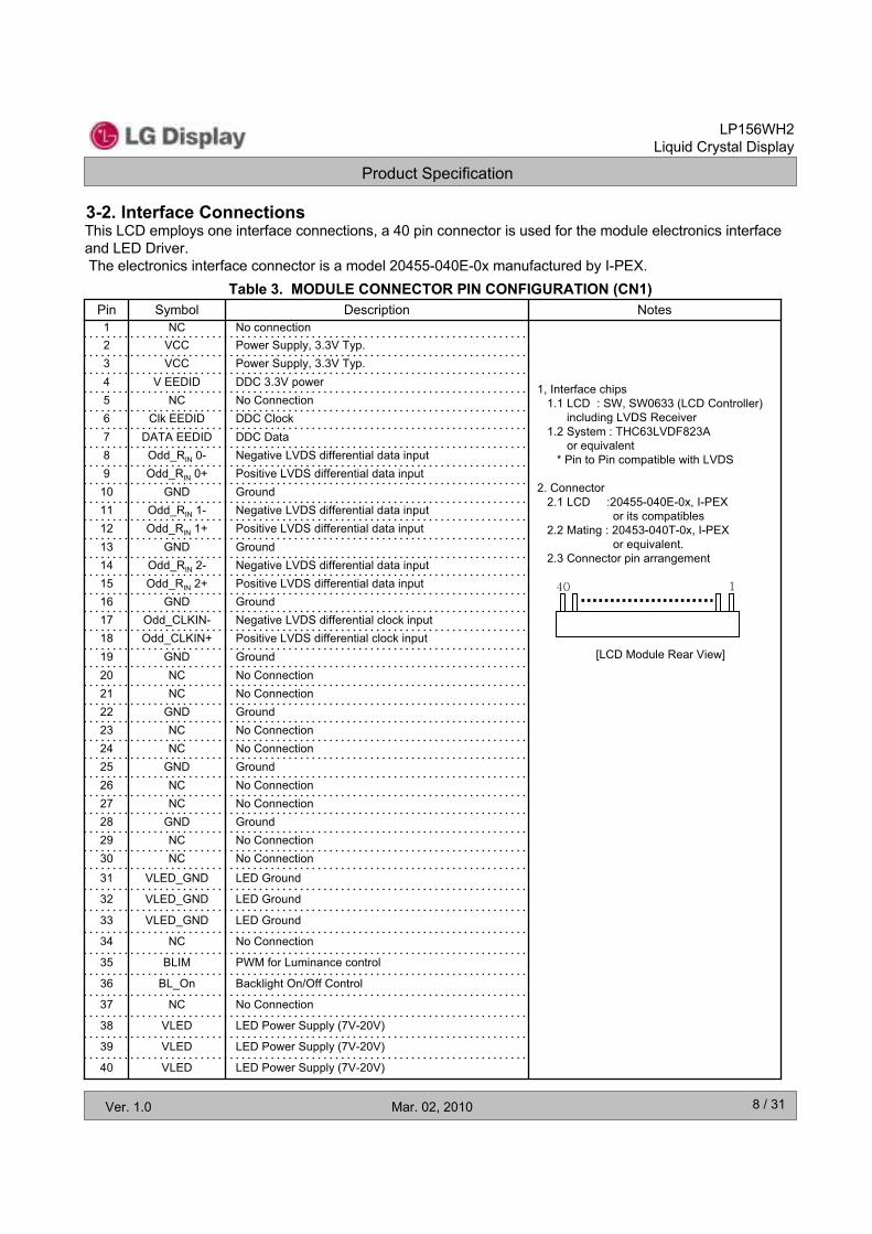
3-2. Interface Connections
Table 3. MODULE CONNECTOR PIN CONFIGURATION (CN1)
No ConnectionNC30
LED Power Supply (7V-20V)VLED40
LED Power Supply (7V-20V)VLED39
LED Power Supply (7V-20V)VLED38
No ConnectionNC37
Backlight On/Off ControlBL_On36
PWM for Luminance controlBLIM35
No ConnectionNC34
LED GroundVLED_GND33
LED GroundVLED_GND32
No ConnectionNC20GroundGND19Positive LVDS differential clock inputOdd_CLKIN+18Negative LVDS differential clock inputOdd_CLKIN-17GroundGND16Positive LVDS differential data inputOdd_RIN 2+15Negative LVDS differential data inputOdd_RIN 2-14GroundGND13Positive LVDS differential data inputOdd_RIN 1+12Negative LVDS differential data inputOdd_RIN 1-11
LED GroundVLED_GND31
Power Supply, 3.3V Typ.VCC2Power Supply, 3.3V Typ.VCC3DDC 3.3V powerV EEDID4No ConnectionNC5DDC ClockClk EEDID6DDC DataDATA EEDID7
Positive LVDS differential data inputOdd_RIN 0+9
No connectionNC1
Negative LVDS differential data inputOdd_RIN 0-8
GroundGND10
GroundGND22No ConnectionNC23No ConnectionNC24GroundGND25No ConnectionNC26No ConnectionNC27GroundGND28No ConnectionNC29
NotesDescriptionSymbolPin
NC No Connection21
1, Interface chips1.1 LCD : SW, SW0633 (LCD Controller)
including LVDS Receiver1.2 System : THC63LVDF823A
or equivalent* Pin to Pin compatible with LVDS
2. Connector2.1 LCD :20455-040E-0x, I-PEX
or its compatibles2.2 Mating : 20453-040T-0x, I-PEX
or equivalent.2.3 Connector pin arrangement
[LCD Module Rear View]
This LCD employs one interface connections, a 40 pin connector is used for the module electronics interface and LED Driver.The electronics interface connector is a model 20455-040E-0x manufactured by I-PEX.
Product Specification
9 / 31
LP156WH2Liquid Crystal Display
Ver. 1.0 Mar. 02, 2010
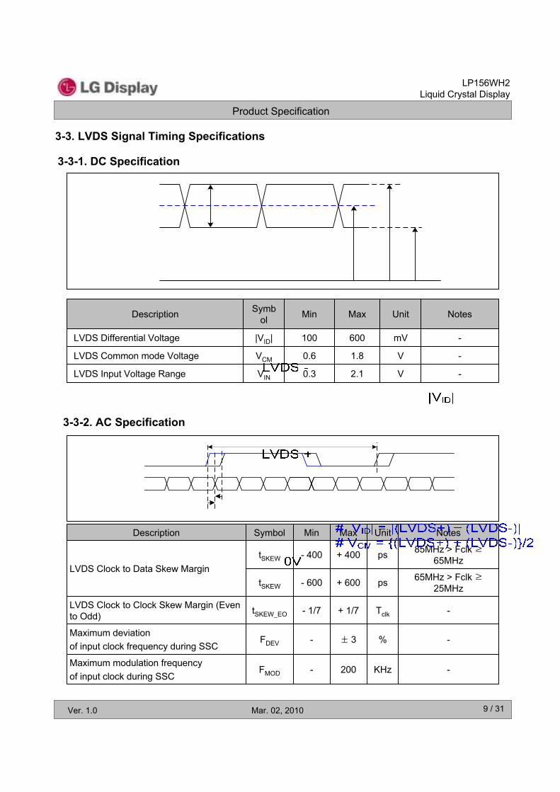
NotesUnitMaxMinSymbolDescription
85MHz > Fclk 65MHzps+ 400- 400tSKEW
LVDS Clock to Data Skew Margin
-
-
-
65MHz > Fclk 25MHz
%3-FDEVMaximum deviation of input clock frequency during SSC
KHz200-FMODMaximum modulation frequency of input clock during SSC
- 1/7
- 600
Tclk+ 1/7tSKEW_EOLVDS Clock to Clock Skew Margin (Even to Odd)
ps+ 600tSKEW
-V2.10.3VINLVDS Input Voltage Range
-V1.80.6VCMLVDS Common mode Voltage
-mV600100|VID|LVDS Differential Voltage
NotesUnitMaxMinSymbolDescription
3-3-1. DC Specification
3-3-2. AC Specification
3-3. LVDS Signal Timing Specifications
Product Specification
10 / 31
LP156WH2Liquid Crystal Display
Ver. 1.0 Mar. 02, 2010
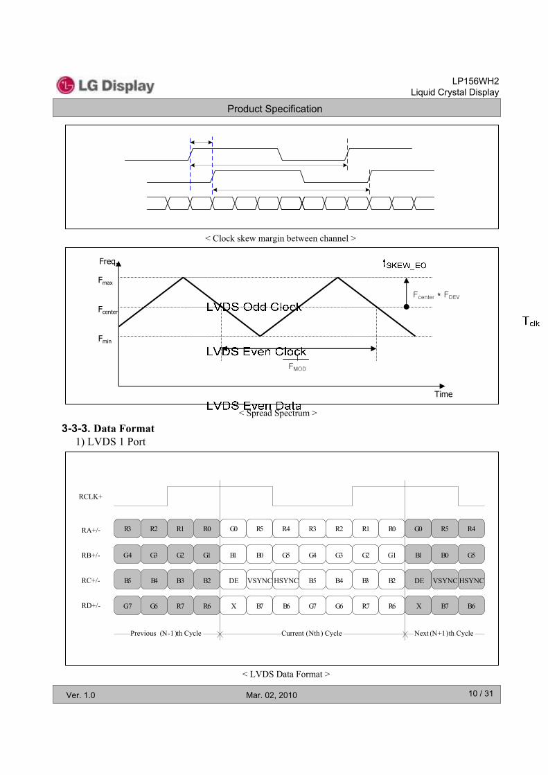
< Clock skew margin between channel >
< LVDS Data Format >
3-3-3. Data Format1) LVDS 1 Port
< Spread Spectrum >
Time
Fcenter
Fmax
Fmin
Freq.
G0 R5 R4 R3 R2 R1 R0
B1 B0 G5 G4 G3 G2 G1
DE VSYNC HSYNC B5 B4 B3 B2
X B7 B6 G7 G6 R7 R6
R1 R0
G2 G1
B3 B2
R7 R6
G0
B1
DE
X
Current (Nth ) Cycle
R5 R4
B0 G5
VSYNC HSYNC
B7 B6
R3 R2
G4 G3
B5 B4
G7 G6
Previous (N-1)th Cycle Next (N+1)th Cycle
RCLK+
RA+/-
RB+/-
RC+/-
RD+/-
Product Specification
11 / 31
LP156WH2Liquid Crystal Display
Ver. 1.0 Mar. 02, 2010
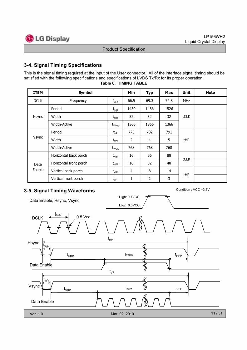
3-4. Signal Timing Specifications
Table 6. TIMING TABLE
This is the signal timing required at the input of the User connector. All of the interface signal timing should be satisfied with the following specifications and specifications of LVDS Tx/Rx for its proper operation.
3-5. Signal Timing Waveforms Condition : VCC =3.3V
Low: 0.3VCC
High: 0.7VCCData Enable, Hsync, Vsync
Hsync
Data Enable
Vsync
Data Enable
tWH
tHP
tHFPtHBP
tVP
tWV
tVBPtVFP
tWHA
tWVA
tCLK 0.5 VccDCLK
768768768tWVAWidth-Active
136613661366tWHAWidth-Active
tCLK885616tHBPHorizontal back porch
483216tHFPHorizontal front porch
tHP1484tVBPVertical back porch
321tVFPVertical front porch
tHP
791782775tVPPeriod
542tWVWidth
323232tWHWidth tCLK
152614861430tHPPeriod
Hsync
Vsync
DataEnable
MHz72.869.366.5fCLKFrequencyDCLK
NoteUnitMaxTypMinSymbolITEM
Product Specification
12 / 31
LP156WH2Liquid Crystal Display
Ver. 1.0 Mar. 02, 2010
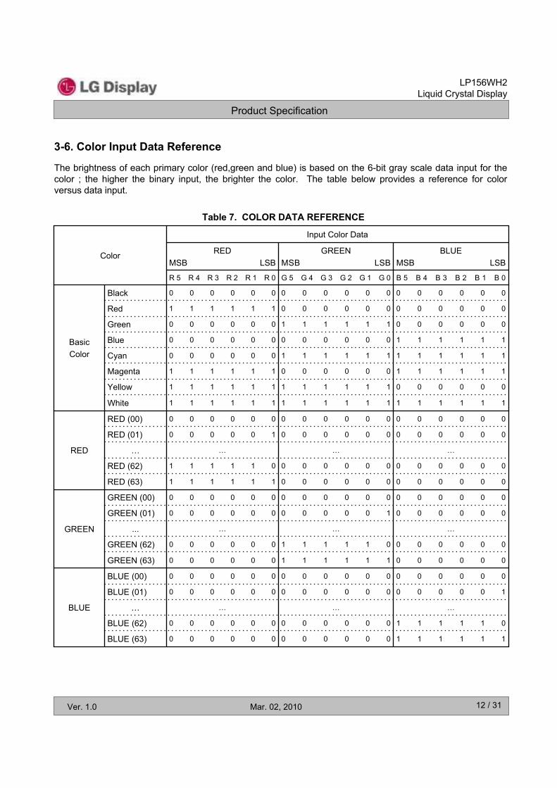
3-6. Color Input Data Reference
The brightness of each primary color (red,green and blue) is based on the 6-bit gray scale data input for thecolor ; the higher the binary input, the brighter the color. The table below provides a reference for color versus data input.
Table 7. COLOR DATA REFERENCE
0 0 0 0 0 00 0 0 0 0 00 0 0 0 0 0GREEN (00)
GREEN
0 0 0 0 0 00 0 0 0 0 10 0 0 0 0 0GREEN (01)
………...
0 0 0 0 0 01 1 1 1 1 00 0 0 0 0 0GREEN (62)
0 0 0 0 0 01 1 1 1 1 10 0 0 0 0 0GREEN (63)
0 0 0 0 0 00 0 0 0 0 00 0 0 0 0 0RED (00)
RED
0 0 0 0 0 00 0 0 0 0 00 0 0 0 0 1RED (01)
…………
0 0 0 0 0 00 0 0 0 0 01 1 1 1 1 0RED (62)
0 0 0 0 0 00 0 0 0 0 01 1 1 1 1 1RED (63)
0 0 0 0 0 10 0 0 0 0 00 0 0 0 0 0BLUE (01)
…………
1 1 1 1 1 00 0 0 0 0 00 0 0 0 0 0BLUE (62)
1 1 1 1 1 10 0 0 0 0 00 0 0 0 0 0BLUE (63)
BLUE (00)
White
Yellow
Magenta
Cyan
Blue
Green
Red
Black 0 0 0 0 0 00 0 0 0 0 00 0 0 0 0 0
BasicColor
0 0 0 0 0 00 0 0 0 0 01 1 1 1 1 1
0 0 0 0 0 01 1 1 1 1 10 0 0 0 0 0
1 1 1 1 1 10 0 0 0 0 00 0 0 0 0 0
1 1 1 1 1 11 1 1 1 1 10 0 0 0 0 0
1 1 1 1 1 10 0 0 0 0 01 1 1 1 1 1
0 0 0 0 0 01 1 1 1 1 11 1 1 1 1 1
1 1 1 1 1 11 1 1 1 1 11 1 1 1 1 1
BLUEMSB LSB
GREENMSB LSB
REDMSB LSB
B 5 B 4 B 3 B 2 B 1 B 0G 5 G 4 G 3 G 2 G 1 G 0R 5 R 4 R 3 R 2 R 1 R 0
0 0 0 0 0 00 0 0 0 0 00 0 0 0 0 0
BLUE
Color
Input Color Data
Product Specification
13 / 31
LP156WH2Liquid Crystal Display
Ver. 1.0 Mar. 02, 2010
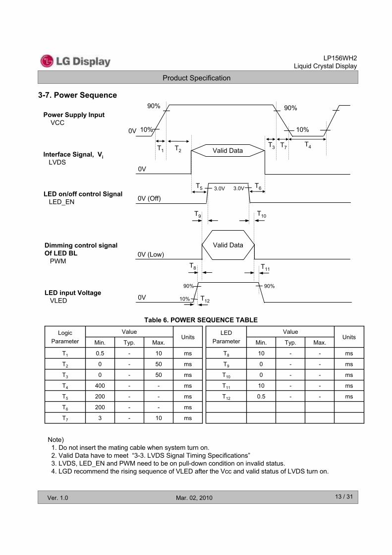
Note)1. Do not insert the mating cable when system turn on. 2. Valid Data have to meet “3-3. LVDS Signal Timing Specifications”3. LVDS, LED_EN and PWM need to be on pull-down condition on invalid status.4. LGD recommend the rising sequence of VLED after the Vcc and valid status of LVDS turn on.
Table 6. POWER SEQUENCE TABLE
ms--0.5T12
ms--10T11
ms--0T10
ms--0T9
ms--10T8
Max.Typ.Min.Units
ValueLEDParameter
ms--200T5
ms--400T4
ms10-3T7
ms--200T6
ms50-0T3
ms50-0T2
ms10-0.5T1
Max.Typ.Min.Units
ValueLogicParameter
3-7. Power Sequence
T7Interface Signal, Vi
LVDS
Power Supply InputVCC
90%
10%10%0V
90%
T1 T2T3 T4
T5 T6
0V
Dimming control signal Of LED BL
PWM0V (Low)
T8
LED input VoltageVLED
T10
LED on/off control SignalLED_EN
T11
T9
Valid Data
0V
Valid Data
0V (Off)
90%
10% T12
90%
3.0V 3.0V
Product Specification
14 / 31
LP156WH2Liquid Crystal Display
Ver. 1.0 Mar. 02, 2010
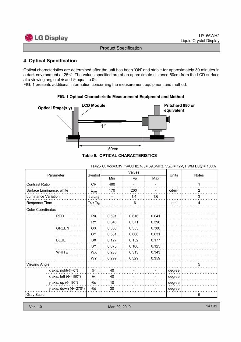
4. Optical Specification
FIG. 1 Optical Characteristic Measurement Equipment and Method
Table 9. OPTICAL CHARACTERISTICS
5Viewing Angle
Color Coordinates
4ms-16-TrR+ TrDResponse Time
0.1250.1000.075BY0.3430.3130.283WXWHITE
y axis, down ( =270 )y axis, up ( =90 )x axis, left ( =180 )x axis, right( =0 ) degree--40r
degree--40ldegree--10udegree--30d
BLUE
0.3590.3290.299WY
6Gray Scale
GREEN
RED
0.3800.3550.330GX0.6310.6060.581GY
0.6410.6160.591RX0.3960.3710.346RY
31.61.4-WHITELuminance Variation
0.1770.1520.127BX
MaxTypMin1--400CRContrast Ratio2cd/m2-200170LWHSurface Luminance, white
Parameter Symbol NotesUnitsValues
LCD ModuleOptical Stage(x,y) Pritchard 880 orequivalent
50cm
Optical characteristics are determined after the unit has been ‘ON’ and stable for approximately 30 minutes in a dark environment at 25 C. The values specified are at an approximate distance 50cm from the LCD surface at a viewing angle of and equal to 0 .FIG. 1 presents additional information concerning the measurement equipment and method.
Ta=25 C, Vcc=3.3V, fV=60Hz, fCLK= 69.3MHz, VLED = 12V, PWM Duty = 100%

Product Specification
15 / 31
LP156WH2Liquid Crystal Display
Ver. 1.0 Mar. 02, 2010
100L6374.17L55
12.21L2321.01L3134.82L3952.49L47
5.36L151.45L7
0L0Luminance [%] (Typ)Gray Level
Note)1. Contrast Ratio(CR) is defined mathematically as
Surface Luminance with all white pixelsContrast Ratio =
Surface Luminance with all black pixels
2. Surface luminance is the average of 5 point across the LCD surface 50cm from the surface withall pixels displaying white. For more information see FIG 1.
LWH = Average(L1,L2, … L5)
3. The variation in surface luminance , The panel total variation ( WHITE) is determined by measuring LNat each test position 1 through 13 and then defined as followed numerical formula.
For more information see FIG 2.
Maximum(L1,L2, … L13)WHITE =
Minimum(L1,L2, … L13)
4. Response time is the time required for the display to transition from white to black (rise time, TrR) andfrom black to white(Decay Time, TrD). For additional information see FIG 3.
5. Viewing angle is the angle at which the contrast ratio is greater than 10. The angles are determined for the horizontal or x axis and the vertical or y axis with respect to the z axis which is normal to theLCD surface. For more information see FIG 4.
6. Gray scale specification * fV = 60Hz

Product Specification
16 / 31
LP156WH2Liquid Crystal Display
Ver. 1.0 Mar. 02, 2010
FIG. 4 Viewing angle
<Dimension of viewing angle range>
Normal YEye
= 0 ,Right
= 180 ,Left
= 270 ,Down
= 90 , Up
FIG. 3 Response Time
The response time is defined as the following figure and shall be measured by switching the input signal for “black” and “white”.
TrR TrD
10090
100
%
Optical
Response
whiteblack
white
<Measuring point for Average Luminance & measuring point for Luminance variation>
: ACTIVE AREAA : H/4 mmB : V/4 mm
POINTS: 13 POINTS
H,V
Active Area
1
32
54
H
A
B
V
6 7 8
9 10
11 12 13
10mm
10mm
FIG. 2 Luminance
Product Specification
17 / 31
LP156WH2Liquid Crystal Display
Ver. 1.0 Mar. 02, 2010
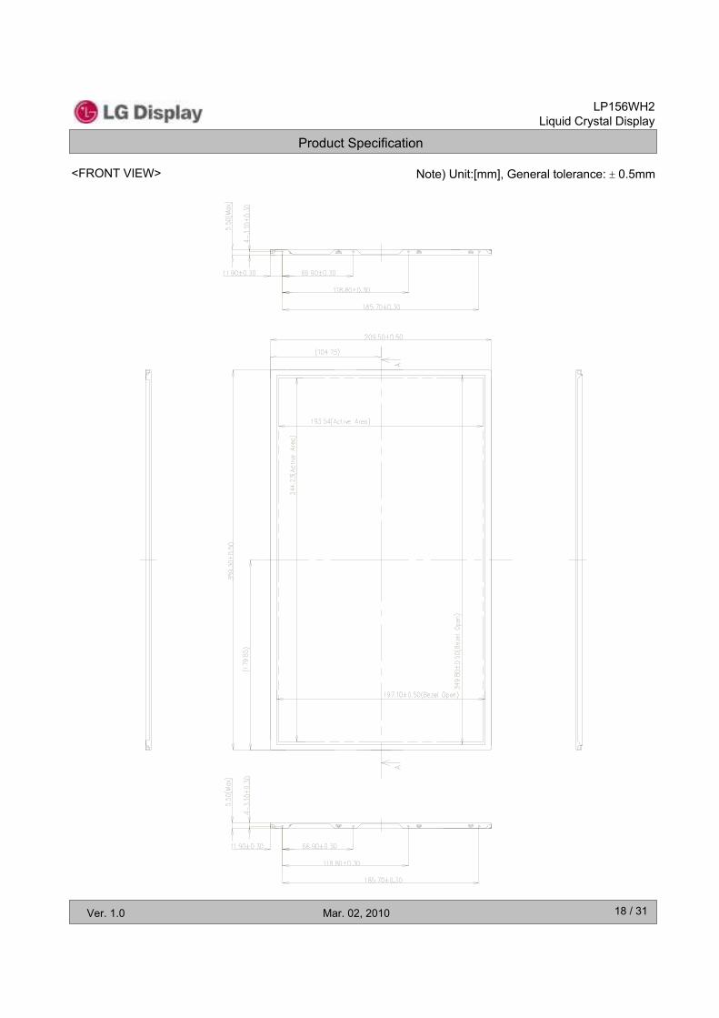
5. Mechanical CharacteristicsThe contents provide general mechanical characteristics for the model LP156WH2. In addition the figuresin the next page are detailed mechanical drawing of the LCD.
193.54 mmVertical
Hard Coating(3H), Glare treatment of the front polarizerSurface Treatment
450g (Max.)Weight
197.1 0.5mmVertical
209.5 0.5mmVertical
5.5mm (max)Thickness
344.23 mmHorizontalActive Display Area
349.8 0.5mmHorizontalBezel Area
359.3 0.5mmHorizontal
Outline Dimension
Product Specification
18 / 31
LP156WH2Liquid Crystal Display
Ver. 1.0 Mar. 02, 2010
<FRONT VIEW> Note) Unit:[mm], General tolerance: 0.5mm

Product Specification
19 / 31
LP156WH2Liquid Crystal Display
Ver. 1.0 Mar. 02, 2010
<REAR VIEW> Note) Unit:[mm], General tolerance: 0.5mm

Product Specification
20 / 31
LP156WH2Liquid Crystal Display
Ver. 1.0 Mar. 02, 2010
[ DETAIL DESCRIPTION OF SIDE MOUNTING SCREW ]
Notes : 1. Screw plated through the method of non-electrolytic nickel plating is preferredto reduce possibility that results in vertical and/or horizontal line defect due tothe conductive particles from screw surface.

Product Specification
21 / 31
LP156WH2Liquid Crystal Display
Ver. 1.0 Mar. 02, 2010
LPL Proposal for system cover design.(Appendix)
Define
Define
1.Rear side of LCM is sensitive against external stress,and previous checkabout interference is highly needed.
2.In case there is something from system cover comes into the boundaryabove,mechanical interference may cause the FOS defects.(Eg: Ripple, White spot..)
Check if antenna cable is sufficiently apart from T-CON of LCD Module.2
1Gap check for securing the enough gap between LCM and System cover.
NO GOOD GOOD
1.If system antenna is overlapped with T-CON,it might be cause the noise.
Max Thickness
A Boundary Line
Sponge
System Cover
LCM Reflector Side

Product Specification
22 / 31
LP156WH2Liquid Crystal Display
Ver. 1.0 Mar. 02, 2010
LPL Proposal for system cover design.
1.COF area needs to be handled with care.
Define
1.At least 2.0mm of gap needs to be secured to prevent the shock related defects.Define
2.”L” type of hinge is recommended than “I” type under shock test.
2.GOOD Wire path design to system side.OK Wire path is located between COFs.
BAD Wire path overlapped with COF area.
4
3Gap check for securing the enough gap between LCMand System hinge.
Checking the path of the System wire.
(“I” TYPE) (“L” TYPE)
COF(D-IC)
HingeGAP:Min2.0mm
Side Mount Screw Hole (4ea)
OkBad Good
#1#2#3
Product Specification
23 / 31
LP156WH2Liquid Crystal Display
Ver. 1.0 Mar. 02, 2010
LPL Proposal for system cover design.
1.CNT area is specially sensitive against external stress,and additional gap by cutting on system cover will be helpful on removing the Ripple.
2.Using a thinner CNT will be better. (eg: FPC type)Define
1.Condition without bracket is good for mechanical noise,and can minimizethe light leakage from deformation of bracket.
Define2.The results shows that there is no difference between the condition
with or without bracket.
Securing additional gap on CNT area..6
5 Using a bracket on the top of LCM is not recommended.
With bracket Without bracket
bracket
User connectorCable pathway.
System cover inner side.
User connectorarea.
cut
A A-1
A~A-1

Product Specification
24 / 31
LP156WH2Liquid Crystal Display
Ver. 1.0 Mar. 02, 2010
6. Reliability
Environment test condition
{ Result Evaluation Criteria }There should be no change which might affect the practical display function when the display qualitytest is conducted under normal operating condition.
0 ~ 10,000 feet (3,048m) 24Hr0 ~ 40,000 feet (12,192m) 24Hr
Altitude operatingstorage / shipment
7
Half sine wave, 180G, 2msone shock of each six faces(I.e. run 180G 2msfor all six faces)
Shock test (non-operating)6
Sine wave, 10 ~ 500 ~ 10Hz, 1.5G, 0.37oct/min3 axis, 1hour/axis
Vibration test (non-operating)5
Ta= 0 C, 240hLow temperature operation test4
Ta= 50 C, 50%RH, 240hHigh temperature operation test3
Ta= -20 C, 240hLow temperature storage test2
Ta= 60 C, 240hHigh temperature storage test1
ConditionsTest ItemNo.
Product Specification
25 / 31
LP156WH2Liquid Crystal Display
Ver. 1.0 Mar. 02, 2010
7. International Standards
7-1. Safety
c) EN 60950-1:2006 + A11:2009, European Committee for Electrotechnical Standardization (CENELEC).Information Technology Equipment - Safety - Part 1 : General Requirements.
a) UL 60950-1, Second Edition, Underwriters Laboratories Inc.Information Technology Equipment - Safety - Part 1 : General Requirements.
b) CAN/CSA C22.2 No.60950-1-07, Second Edition, Canadian Standards Association.Information Technology Equipment - Safety - Part 1 : General Requirements.
d) IEC 60950-1:2005, Second Edition, The International Electrotechnical Commission (IEC).Information Technology Equipment - Safety - Part 1 : General Requirements.
7-3. Environment
a) RoHS, Directive 2002/95/EC of the European Parliament and of the council of 27 January 2003
7-2. EMC
a) ANSI C63.4 “American National Standard for Methods of Measurement of Radio-Noise Emissions from Low-Voltage Electrical and Electronic Equipment in the Range of 9 kHz to 40 GHz.”American National Standards Institute (ANSI), 2003.
b) CISPR 22 “Information technology equipment – Radio disturbance characteristics – Limit and methods of measurement." International Special Committee on Radio Interference (CISPR), 2005.
c) CISPR 13 “Sound and television broadcast receivers and associated equipment – Radio disturbance characteristics – Limits and method of measurement." International Special Committee on Radio Interference (CISPR), 2006.
Product Specification
26 / 31
LP156WH2Liquid Crystal Display
Ver. 1.0 Mar. 02, 2010
8. Packing
8-2. Packing Form
a) Package quantity in one box : 22 pcs
b) Box Size : 440x360x260mm
8-1. Designation of Lot Marka) Lot Mark
A B C D E F G H I J K L M
A,B,C : SIZE(INCH) D : YEAR E : MONTH F ~ M : SERIAL NO.
Note1. YEAR
2. MONTH
Mark
Year
0
2010
6
2006
7
2007
8
2008
9
2009
4
2004
5
2005
321
200320022001
B
Nov
Mark
Month
A
Oct
6
Jun
7
Jul
8
Aug
9
Sep
4
Apr
5
May
C321
DecMarFebJan
b) Location of Lot Mark
Serial No. is printed on the label. The label is attached to the backside of the LCD module.This is subject to change without prior notice.
Product Specification
27 / 31
LP156WH2Liquid Crystal Display
Ver. 1.0 Mar. 02, 2010
9. PRECAUTIONS
Please pay attention to the followings when you use this TFT LCD module.
9-1. MOUNTING PRECAUTIONS(1) You must mount a module using holes arranged in four corners or four sides.(2) You should consider the mounting structure so that uneven force (ex. Twisted stress) is not applied to the
module. And the case on which a module is mounted should have sufficient strength so that external force is not transmitted directly to the module.
(3) Please attach the surface transparent protective plate to the surface in order to protect the polarizer.Transparent protective plate should have sufficient strength in order to the resist external force.
(4) You should adopt radiation structure to satisfy the temperature specification.(5) Acetic acid type and chlorine type materials for the cover case are not desirable because the former
generates corrosive gas of attacking the polarizer at high temperature and the latter causes circuit break by electro-chemical reaction.
(6) Do not touch, push or rub the exposed polarizers with glass, tweezers or anything harder than HBpencil lead. And please do not rub with dust clothes with chemical treatment.Do not touch the surface of polarizer for bare hand or greasy cloth.(Some cosmetics are detrimentalto the polarizer.)
(7) When the surface becomes dusty, please wipe gently with absorbent cotton or other soft materials like chamois soaks with petroleum benzene. Normal-hexane is recommended for cleaning the adhesives used to attach front / rear polarizers. Do not use acetone, toluene and alcohol because they cause chemical damage to the polarizer.
(8) Wipe off saliva or water drops as soon as possible. Their long time contact with polarizer causes deformations and color fading.
(9) Do not open the case because inside circuits do not have sufficient strength.
9-2. OPERATING PRECAUTIONS
(1) The spike noise causes the mis-operation of circuits. It should be lower than following voltage : V= 200mV(Over and under shoot voltage)
(2) Response time depends on the temperature.(In lower temperature, it becomes longer.)(3) Brightness depends on the temperature. (In lower temperature, it becomes lower.)
And in lower temperature, response time(required time that brightness is stable after turned on) becomeslonger.
(4) Be careful for condensation at sudden temperature change. Condensation makes damage to polarizer or electrical contacted parts. And after fading condensation, smear or spot will occur.
(5) When fixed patterns are displayed for a long time, remnant image is likely to occur.(6) Module has high frequency circuits. Sufficient suppression to the electromagnetic interference shall be
done by system manufacturers. Grounding and shielding methods may be important to minimized theinterference.

Product Specification
28 / 31
LP156WH2Liquid Crystal Display
Ver. 1.0 Mar. 02, 2010
Since a module is composed of electronic circuits, it is not strong to electrostatic discharge. Make certain that treatment persons are connected to ground through wrist band etc. And don’t touch interface pin directly.
9-3. ELECTROSTATIC DISCHARGE CONTROL
Strong light exposure causes degradation of polarizer and color filter.
9-4. PRECAUTIONS FOR STRONG LIGHT EXPOSURE
9-5. STORAGE
(1) When the protection film is peeled off, static electricity is generated between the film and polarizer.This should be peeled off slowly and carefully by people who are electrically grounded and with wellion-blown equipment or in such a condition, etc.
(2) The protection film is attached to the polarizer with a small amount of glue. If some stress is appliedto rub the protection film against the polarizer during the time you peel off the film, the glue is apt toremain on the polarizer.Please carefully peel off the protection film without rubbing it against the polarizer.
(3) When the module with protection film attached is stored for a long time, sometimes there remains avery small amount of glue still on the polarizer after the protection film is peeled off.
(4) You can remove the glue easily. When the glue remains on the polarizer surface or its vestige isrecognized, please wipe them off with absorbent cotton waste or other soft material like chamoissoaked with normal-hexane.
9-6. HANDLING PRECAUTIONS FOR PROTECTION FILM
When storing modules as spares for a long time, the following precautions are necessary.
(1) Store them in a dark place. Do not expose the module to sunlight or fluorescent light. Keep the temperature between 5 C and 35 C at normal humidity.
(2) The polarizer surface should not come in contact with any other object.It is recommended that they be stored in the container in which they were shipped.
Product Specification
29 / 31
LP156WH2Liquid Crystal Display
Ver. 1.0 Mar. 02, 2010
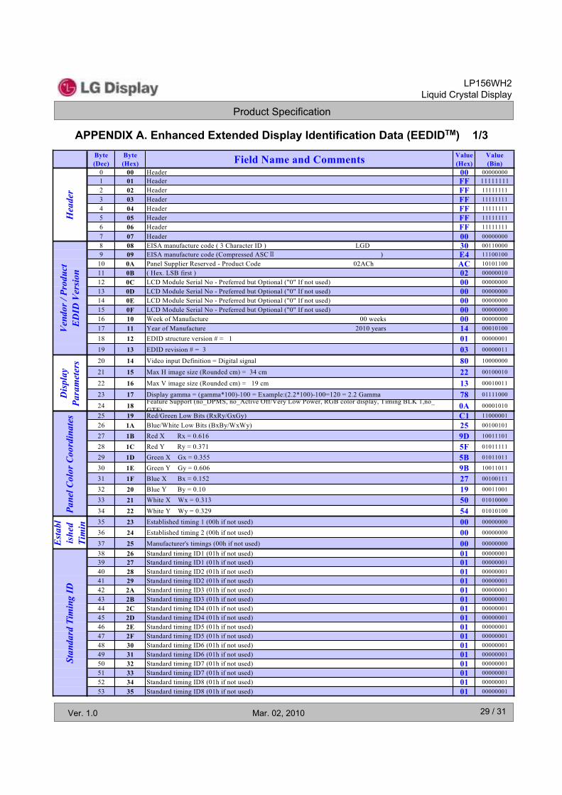
APPENDIX A. Enhanced Extended Display Identification Data (EEDIDTM) 1/3Byte(Dec)
Byte(Hex) Field Name and Comments Value
(Hex)Value(Bin)
0 00 Header 00 000000001 01 Header FF 111111112 02 Header FF 111111113 03 Header FF 111111114 04 Header FF 111111115 05 Header FF 111111116 06 Header FF 111111117 07 Header 00 000000008 08 EISA manufacture code ( 3 Character ID ) LGD 30 001100009 09 EISA manufacture code (Compressed ASC ) E4 11100100
10 0A Panel Supplier Reserved - Product Code 02ACh AC 1010110011 0B ( Hex. LSB first ) 02 0000001012 0C LCD Module Serial No - Preferred but Optional ("0" If not used) 00 0000000013 0D LCD Module Serial No - Preferred but Optional ("0" If not used) 00 0000000014 0E LCD Module Serial No - Preferred but Optional ("0" If not used) 00 0000000015 0F LCD Module Serial No - Preferred but Optional ("0" If not used) 00 0000000016 10 Week of Manufacture 00 weeks 00 0000000017 11 Year of Manufacture 2010 years 14 00010100
18 12 EDID structure version # = 1 01 00000001
19 13 EDID revision # = 3 03 00000011
20 14 Video input Definition = Digital signal 80 10000000
21 15 Max H image size (Rounded cm) = 34 cm 22 00100010
22 16 Max V image size (Rounded cm) = 19 cm 13 00010011
23 17 Display gamma = (gamma*100)-100 = Example:(2.2*100)-100=120 = 2.2 Gamma 78 01111000
24 18 Feature Support (no_DPMS, no_Active Off/Very Low Power, RGB color display, Timing BLK 1,no_GTF) 0A 00001010
25 19 Red/Green Low Bits (RxRy/GxGy) C1 1100000126 1A Blue/White Low Bits (BxBy/WxWy) 25 00100101
27 1B Red X Rx = 0.616 9D 10011101
28 1C Red Y Ry = 0.371 5F 01011111
29 1D Green X Gx = 0.355 5B 01011011
30 1E Green Y Gy = 0.606 9B 10011011
31 1F Blue X Bx = 0.152 27 00100111
32 20 Blue Y By = 0.10 19 00011001
33 21 White X Wx = 0.313 50 01010000
34 22 White Y Wy = 0.329 54 01010100
35 23 Established timing 1 (00h if not used) 00 00000000
36 24 Established timing 2 (00h if not used) 00 00000000
37 25 Manufacturer's timings (00h if not used) 00 00000000
38 26 Standard timing ID1 (01h if not used) 01 0000000139 27 Standard timing ID1 (01h if not used) 01 0000000140 28 Standard timing ID2 (01h if not used) 01 0000000141 29 Standard timing ID2 (01h if not used) 01 0000000142 2A Standard timing ID3 (01h if not used) 01 0000000143 2B Standard timing ID3 (01h if not used) 01 0000000144 2C Standard timing ID4 (01h if not used) 01 0000000145 2D Standard timing ID4 (01h if not used) 01 0000000146 2E Standard timing ID5 (01h if not used) 01 0000000147 2F Standard timing ID5 (01h if not used) 01 0000000148 30 Standard timing ID6 (01h if not used) 01 0000000149 31 Standard timing ID6 (01h if not used) 01 0000000150 32 Standard timing ID7 (01h if not used) 01 0000000151 33 Standard timing ID7 (01h if not used) 01 0000000152 34 Standard timing ID8 (01h if not used) 01 0000000153 35 Standard timing ID8 (01h if not used) 01 00000001
Hea
der
Ven
dor /
Pro
duct
ED
ID V
ersi
onD
ispl
ayPa
ram
eter
sPa
nel C
olor
Coo
rdin
ates
Est
abl
ishe
dTi
min
Stan
dard
Tim
ing
ID

Product Specification
30 / 31
LP156WH2Liquid Crystal Display
Ver. 1.0 Mar. 02, 2010
APPENDIX A. Enhanced Extended Display Identification Data (EEDIDTM) 2/3Byte(Dec)
Byte(Hex) Field Name and Comments Value
(Hex)Value(Bin)
54 36 Pixel Clock/10,000 (LSB) 69.3 MHz @ 59.6Hz 12 0001001055 37 Pixel Clock/10,000 (MSB) 1B 00011011
56 38 Horizontal Active (lower 8 bits) 1366 Pixels 56 01010110
57 39 Horizontal Blanking(Thp-HA) (lower 8 bits) 120 Pixels 78 01111000
58 3A Horizontal Active / Horizontal Blanking(Thp-HA) (upper 4:4bits) 50 01010000
59 3B Vertical Avtive 768 Lines 00 00000000
60 3C Vertical Blanking (Tvp-HA) (DE Blanking typ.for DE only panels) 14 Lines 0E 00001110
61 3D Vertical Active : Vertical Blanking (Tvp-HA) (upper 4:4bits) 30 00110000
62 3E Horizontal Sync. Offset (Thfp) 32 Pixels 20 00100000
63 3F Horizontal Sync Pulse Width (HSPW) 32 Pixels 20 00100000
64 40 Vertical Sync Offset(Tvfp) : Sync Width (VSPW) 2 Lines : 4 Lines 24 00100100
65 41 Horizontal Vertical Sync Offset/Width (upper 2bits) 00 00000000
66 42 Horizontal Image Size (mm) 344 mm 58 01011000
67 43 Vertical Image Size (mm) 194 mm C2 11000010
68 44 Horizontal Image Size / Vertical Image Size 10 00010000
69 45 Horizontal Border = 0 (Zero for Notebook LCD) 00 00000000
70 46 Vertical Border = 0 (Zero for Notebook LCD) 00 00000000
71 47Non-Interlace, Normal display, no stereo, Digital Separate ( Vsync_NEG, Hsync_NEG ), DE only note :LSB is set to '1' if panel is DE-timing only. H/V can be ignored. 19 00011001
72 48 Flag 00 0000000073 49 Flag 00 00000000
74 4A Flag 00 00000000
75 4B Data Type Tag (Descriptor Defined by manufacturer ) 00 00000000
76 4C Flag 00 00000000
77 4D Descriptor Defined by manufacturer 00 00000000
78 4E Descriptor Defined by manufacturer 00 00000000
79 4F Descriptor Defined by manufacturer 00 00000000
80 50 Descriptor Defined by manufacturer 00 00000000
81 51 Descriptor Defined by manufacturer 00 00000000
82 52 Descriptor Defined by manufacturer 00 00000000
83 53 Descriptor Defined by manufacturer 00 00000000
84 54 Descriptor Defined by manufacturer 00 00000000
85 55 Descriptor Defined by manufacturer 00 00000000
86 56 Descriptor Defined by manufacturer 00 00000000
87 57 Descriptor Defined by manufacturer 00 00000000
88 58 Descriptor Defined by manufacturer 00 00000000
89 59 Descriptor Defined by manufacturer 00 00000000
90 5A Flag 00 0000000091 5B Flag 00 00000000
92 5C Flag 00 00000000
93 5D Data Type Tag ( ASCII String ) FE 11111110
94 5E Flag 00 00000000
95 5F ASCII String L 4C 01001100
96 60 ASCII String G 47 01000111
97 61 ASCII String 20 00100000
98 62 ASCII String D 44 01000100
99 63 ASCII String i 69 01101001
100 64 ASCII String s 73 01110011
101 65 ASCII String p 70 01110000
102 66 ASCII String l 6C 01101100
103 67 ASCII String a 61 01100001
104 68 ASCII String y 79 01111001
105 69 Manufacturer P/N(If<13 char--> 0Ah, then terminate with ASC 0A 00001010
106 6A Manufacturer P/N(If<13 char--> 0Ah, then terminate with ASC 20 00100000
107 6B Manufacturer P/N(If<13 char--> 0Ah, then terminate with ASC 20 00100000
Tim
ing
Des
crip
tor #
1Ti
min
g D
escr
ipto
r #2
Tim
ing
Des
crip
tor #
3
Product Specification
31 / 31
LP156WH2Liquid Crystal Display
Ver. 1.0 Mar. 02, 2010
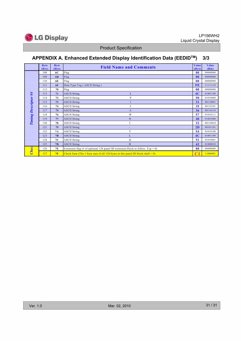
APPENDIX A. Enhanced Extended Display Identification Data (EEDIDTM) 3/3Byte(Dec)
Byte(Hex) Field Name and Comments Value
(Hex)Value(Bin)
108 6C Flag 00 00000000
109 6D Flag 00 00000000
110 6E Flag 00 00000000
111 6F Data Type Tag ( ASCII String ) FE 11111110
112 70 Flag 00 00000000
113 71 ASCII String L 4C 01001100
114 72 ASCII String P 50 01010000
115 73 ASCII String 1 31 00110001
116 74 ASCII String 5 35 00110101
117 75 ASCII String 6 36 00110110
118 76 ASCII String W 57 01010111
119 77 ASCII String H 48 01001000
120 78 ASCII String 2 32 00110010
121 79 ASCII String - 2D 00101101
122 7A ASCII String T 54 01010100
123 7B ASCII String L 4C 01001100
124 7C ASCII String Q 51 01010001
125 7D ASCII String B 42 01000010
126 7E Extension flag (# of optional 128 panel ID extension block to follow, Typ = 0) 00 00000000
127 7F Check Sum (The 1-byte sum of all 128 bytes in this panel ID block shall = 0) C1 11000001
Tim
ing
Des
crip
tor #
4C
heck