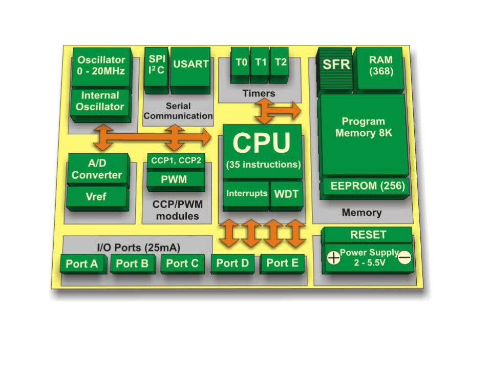
Special Function Register In addition to the registers which do not have any special and...
44
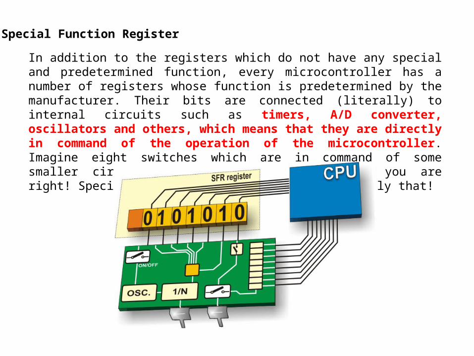
Special Function Register In addition to the registers which do not have any special and predetermined function, every microcontroller has a number of registers whose function is predetermined by the manufacturer. Their bits are connected (literally) to internal circuits such as timers, A/D converter, oscillators and others, which means that they are directly in command of the operation of the microcontroller. Imagine eight switches which are in command of some smaller circuits within the microcontroller- you are right! Special Function Registers (SFRs) do exactly that!
-
Upload
leslie-rosalyn-gardner -
Category
Documents
-
view
219 -
download
0
Transcript of Special Function Register In addition to the registers which do not have any special and...
Special Function Register
In addition to the registers which do not have any special and predetermined function, every microcontroller has a number of registers whose function is predetermined by the manufacturer. Their bits are connected (literally) to internal circuits such as timers, A/D converter, oscillators and others, which means that they are directly in command of the operation of the microcontroller. Imagine eight switches which are in command of some smaller circuits within the microcontroller- you are right! Special Function Registers (SFRs) do exactly that!
Input/Output Ports
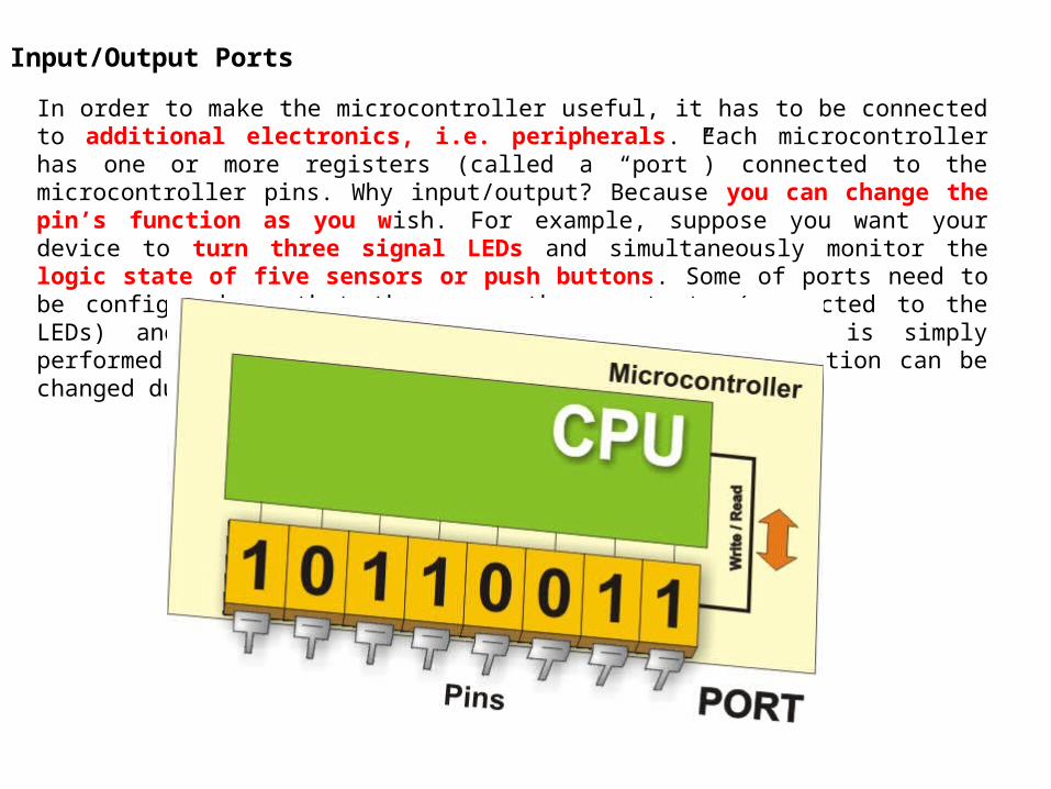
In order to make the microcontroller useful, it has to be connected to additional electronics, i.e. peripherals. Each microcontroller has one or more registers (called a “port”) connected to the microcontroller pins. Why input/output? Because you can change the pin’s function as you wish. For example, suppose you want your device to turn three signal LEDs and simultaneously monitor the logic state of five sensors or push buttons. Some of ports need to be configured so that there are three outputs (connected to the LEDs) and five inputs (connected to sensors). It is simply performed by software, which means that the pin’s function can be changed during operation.
One of the more important specifications of input/output (I/O) pins is the maximum current they can handle.
Another way of putting it is that the maximum current stated in the data specifications sheet for the microprocessor is shared across all I/O ports. Usually, each I/O port is under control of another SFR, which means that each bit of that register determines the state of the corresponding microcontroller pin.
Memory Unit
Memory is part of the microcontroller used for data storage. The easiest way to explain it is to compare it with a filing cabinet with many drawers. Suppose, the drawers are clearly marked so that it is easy to access any of them. It is easy enough to find out the contents of the drawer by reading the label on the front of the drawer.

Each memory address corresponds to one memory location. The content of any location becomes known by its addressing. Memory can either be written to or read from. There are several types of memory within the microcontroller.
Read Only Memory (ROM)
ROM (Read Only Memory) is used to permanently save the program being executed. The size of a program that can be written depends on the size of this memory. Today’s microcontrollers commonly use 16-bit addressing, which means that they are able to address up to 64 Kb of memory, i.e. 65535 locations. As a novice, your program will rarely exceed the limit of several hundred instructions. There are several types of ROM.
Masked ROM
Microcontrollers containing this ROM are reserved for the great manufacturers. Program is loaded into the chip by the manufacturer.
One Time Programmable ROM (OTP ROM)
If the microcontroller contains this memory, you can download a program into this memory, but the process of program downloading is a “one-way ticket”, meaning that it can be done only once. If an error is detected after downloading, the only thing you can do is to download the corrected program to another chip.

UV Erasable Programmable ROM (UV EPROM).
Both the manufacturing process and characteristics of this memory are completely identical to OTP ROM. However, the package of this microcontroller has a recognizable “window” on the upper side. It enables the surface of the silicon chip inside to be lit by an UV lamp, which effectively erases and program from the ROM. Installation of this window is very complicated, which normally affects the price. From our point of view, unfortunately- negative...
Flash memory.
This type of memory was invented in the 80s in the laboratories of INTEL and were represented as the successor to the UV EPROM. Since the contents of this memory can be written and cleared practically an unlimited number of times, the microcontrollers with Flash ROM are ideal for learning, experimentation and small-scale manufacture. Because of its popularity, the most microcontrollers are manufactured in flash versions today. So, if you are going to buy a microcontroller, the type to look for is definitely Flash!
Random Access Memory (RAM)
Once the power supply is off the contents of RAM (Random Access Memory) is cleared. It is used for temporary storing data and intermediate results created and used during the operation of the microcontroller. For example, if the program performs an addition (of whatever), it is necessary to have a register representing what in everyday life is called the “sum”. For that purpose, one of the registers in RAM is called the “sum” and used for storing results of addition.
Electrically Erasable Programmable ROM (EEPROM)
The contents of the EEPROM may be changed during operation (similar to RAM), but remains permanently saved even upon the power supply goes off (similar to ROM). Accordingly, an EEPROM is often used to store values, created during operation, which must be permanently saved. For example, if you design an electronic lock or an alarm, it would be great to enable the user to create and enter a password, but useless if it is lost every time the power supply goes off. The ideal solution is the microcontroller with an embedded EEPROM.
Interrupt
The most programs use interrupts in regular program execution. The purpose of the microcontroller is mainly to react on changes in its surrounding. In other words, when some event takes place, the microcontroller does something... For example, when you push a button on a remote controller, the microcontroller will register it and respond to the order by changing a channel, turn the volume up or down etc. If the microcontroller spent most of its time endlessly a few buttons for hours or days... It would not be practical.
The microcontroller has learnt during its evolution a trick. Instead of checking each pin or bit constantly, the microcontroller delegates the “wait issue” to the “specialist” which will react only when something attention worthy happens.
The signal which informs the central processor about such an event is called an INTERRUPT.
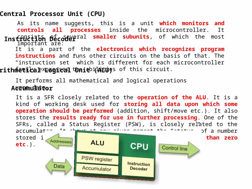
Central Processor Unit (CPU)As its name suggests, this is a unit which monitors and controls all processes inside the microcontroller. It consists of several smaller subunits, of which the most important are:
Instruction Decoder
It is a part of the electronics which recognizes program instructions and runs other circuits on the basis of that. The “instruction set” which is different for each microcontroller family expresses the abilities of this circuit.Arithmetical Logical Unit (ALU)
It performs all mathematical and logical operations upon data.Accumulator It is a SFR closely related to the operation of the ALU. It is a kind of working desk used for storing all data upon which some operation should be performed (addition, shift/move etc.). It also stores the results ready for use in further processing. One of the SFRs, called a Status Register (PSW), is closely related to the accumulator. It shows at any given moment the “status” of a number stored in the accumulator (number is greater or less than zero etc.).
Bus
Physically, the bus consists of 8, 16 or more wires. There are two types of buses: the address bus and the data bus. The address bus consists of as many lines as necessary for memory addressing. It is used to transmit the address from the CPU to the memory. The data bus is as wide as the data, in our case it is 8 bits or wires wide. It is used to connect all circuits inside the microcontroller.
Serial CommunicationParallel connections between the microcontroller and peripherals via input/output ports is the ideal solution for shorter distances- up to several meters. However, in other cases - when it is necessary to establish communication between two devices on longer distances it is not possible to use a parallel connection - such a simple solution is out of question. In these situations, serial communication is the best solution.Today, most microcontrollers have built in several different systems for serial communication as a standard equipment. Which of these systems will be used depends on many factors of which the most important are:
1.How many devices the microcontroller has to exchange data with?2.How fast the data exchange has to be?3.What is the distance between devices?4.Is it necessary to send and receive data simultaneously?
One of the most important things concerning serial communication is the Protocol which should be strictly observed. It is a set of rules which must be applied in order that the devices can correctly interpret data they mutually exchange. Fortunately, the microcontrollers automatically take care of this, so the work of the programmer/user is reduced to simple write (data to be sent) and read (received data).
Baud Rate
The term Baud rate is commonly used to denote the number of bits transferred per second [bps].
The most commonly used serial communication systems are:
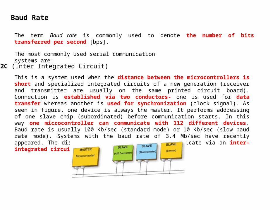
I2C (Inter Integrated Circuit)
This is a system used when the distance between the microcontrollers is short and specialized integrated circuits of a new generation (receiver and transmitter are usually on the same printed circuit board). Connection is established via two conductors- one is used for data transfer whereas another is used for synchronization (clock signal). As seen in figure, one device is always the master. It performs addressing of one slave chip (subordinated) before communication starts. In this way one microcontroller can communicate with 112 different devices. Baud rate is usually 100 Kb/sec (standard mode) or 10 Kb/sec (slow baud rate mode). Systems with the baud rate of 3.4 Mb/sec have recently appeared. The distance between devices which communicate via an inter-integrated circuit bus is limited to several meters.
SPI (Serial Peripheral Interface Bus)
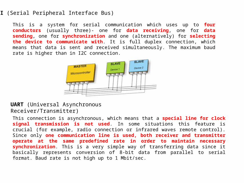
This is a system for serial communication which uses up to four conductors (usually three)- one for data receiving, one for data sending, one for synchronization and one (alternatively) for selecting the device to communicate with. It is full duplex connection, which means that data is sent and received simultaneously. The maximum baud rate is higher than in I2C connection.
UART (Universal Asynchronous Receiver/Transmitter)
This connection is asynchronous, which means that a special line for clock signal transmission is not used. In some situations this feature is crucial (for example, radio connection or infrared waves remote control). Since only one communication line is used, both receiver and transmitter operate at the same predefined rate in order to maintain necessary synchronization. This is a very simple way of transferring data since it basically represents conversion of 8-bit data from parallel to serial format. Baud rate is not high up to 1 Mbit/sec.

Oscillator
Even pulses coming from the oscillator enable harmonic and synchronous operation of all circuits of the microcontroller. The oscillator module is usually configured to use quartz crystal or ceramic resonator for frequency stabilization. Furthermore, it can also operate without elements for frequency stabilization (like RC oscillator). It is important to say that instructions are not executed at the rate imposed by the oscillator itself, but several times slower. It happens because each instruction is executed in several steps. In some microcontrollers, the same number of cycles is needed to execute any instruction, while in others, the execution time is not the same for all instructions. Accordingly, if the system uses quartz crystal with a frequency of 20 MHz, execution time of an instruction is not 50nS, but 200, 400 or 800 nS, depending on the type of Microcontroller Unit (MCU)!
Power supply circuit
There are two things worth attention concerning the microcontroller power supply circuit:
Brown-out is a potentially dangerous state which occurs at the moment the microcontroller is being turned off or in situations when power supply voltage drops to the limit due to electric noise. As the microcontroller consists of several circuits which have different operating voltage levels, this state can cause its out-of-control performance. In order to prevent it, the microcontroller usually has built-in circuit for brown out reset. This circuit immediately resets the whole electronics when the voltage level drops below the limit.
Reset pin is usually marked as MCLR (Master Clear Reset) and serves for external reset of the microcontroller by applying logic zero (0) or one (1), depending on type of the microcontroller. In case the brown out circuit is not built in, a simple external circuit for brown out reset can be connected to this pin.
Timers/Counters
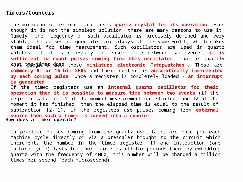
The microcontroller oscillator uses quartz crystal for its operation. Even though it is not the simplest solution, there are many reasons to use it. Namely, the frequency of such oscillator is precisely defined and very stable, the pulses it generates are always of the same width, which makes them ideal for time measurement. Such oscillators are used in quartz watches. If it is necessary to measure time between two events, it is sufficient to count pulses coming from this oscillator. That is exactly what the timer does.
Most programs use these miniature electronic “stopwatches”. These are commonly 8- or 16-bit SFRs and their content is automatically incremented by each coming pulse. Once a register is completely loaded - an interrupt is generated!
If the timer registers use an internal quartz oscillator for their operation then it is possible to measure time between two events (if the register value is T1 at the moment measurement has started, and T2 at the moment it has finished, then the elapsed time is equal to the result of subtraction T2-T1). If the registers use pulses coming from external source then such a timer is turned into a counter.
How does a timer operate?
In practice pulses coming from the quartz oscillator are once per each machine cycle directly or via a prescaler brought to the circuit which increments the number in the timer register. If one instruction (one machine cycle) lasts for four quartz oscillator periods then, by embedding quartz with the frequency of 4MHz, this number will be changed a million times per second (each microsecond).
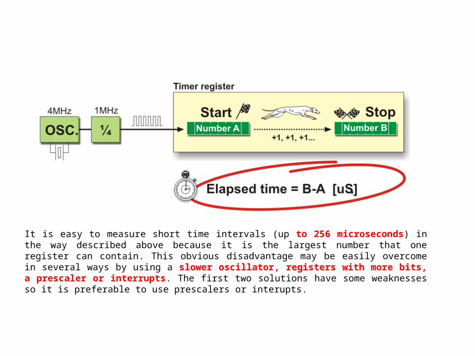
It is easy to measure short time intervals (up to 256 microseconds) in the way described above because it is the largest number that one register can contain. This obvious disadvantage may be easily overcome in several ways by using a slower oscillator, registers with more bits, a prescaler or interrupts. The first two solutions have some weaknesses so it is preferable to use prescalers or interupts.
Using prescaler in timer operating
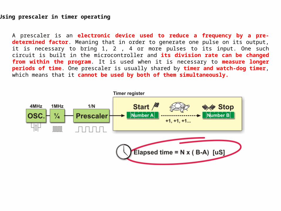
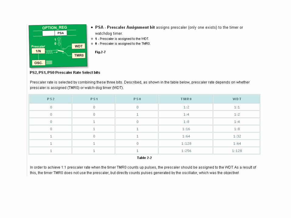
A prescaler is an electronic device used to reduce a frequency by a pre-determined factor. Meaning that in order to generate one pulse on its output, it is necessary to bring 1, 2 , 4 or more pulses to its input. One such circuit is built in the microcontroller and its division rate can be changed from within the program. It is used when it is necessary to measure longer periods of time. One prescaler is usually shared by timer and watch-dog timer, which means that it cannot be used by both of them simultaneously.
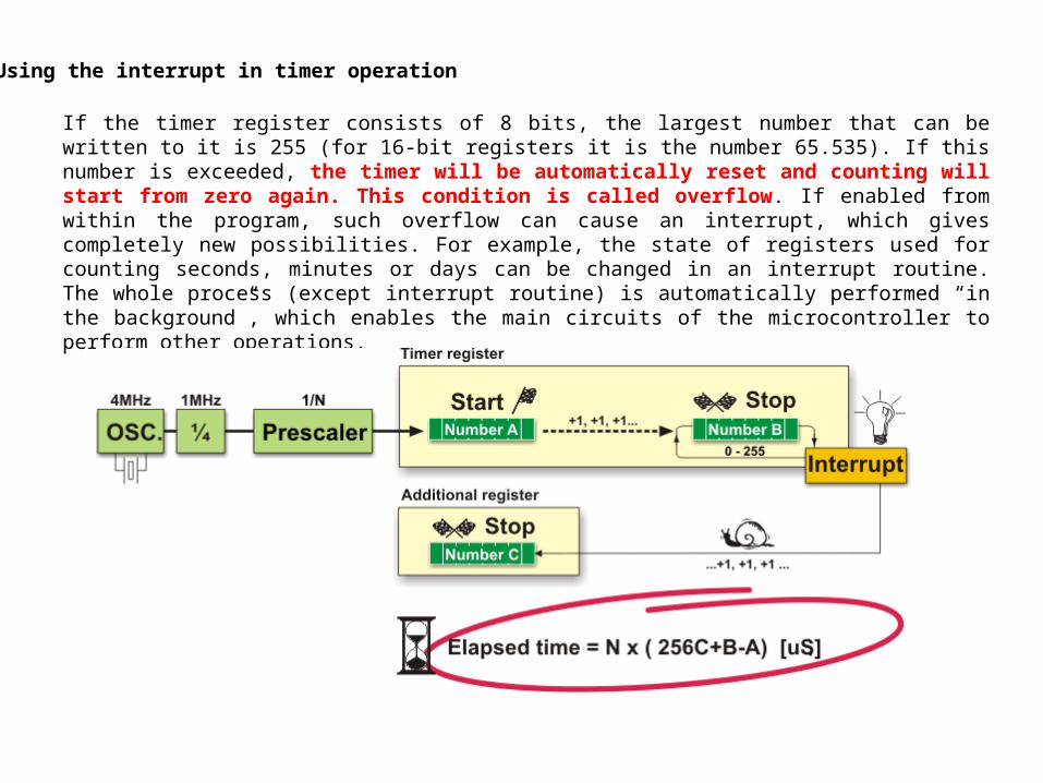
Using the interrupt in timer operation
If the timer register consists of 8 bits, the largest number that can be written to it is 255 (for 16-bit registers it is the number 65.535). If this number is exceeded, the timer will be automatically reset and counting will start from zero again. This condition is called overflow. If enabled from within the program, such overflow can cause an interrupt, which gives completely new possibilities. For example, the state of registers used for counting seconds, minutes or days can be changed in an interrupt routine. The whole process (except interrupt routine) is automatically performed “in the background”, which enables the main circuits of the microcontroller to perform other operations.

Counters
If a timer is supplying pulses into the microcontroller input pin then it turns into a counter. Clearly, It is the same electronic circuit. The only difference is that in this case pulses to be counted come through the ports and their duration (width) is mostly not defined. This is why they cannot be used for time measurement, but can be used to measure anything else: products on an assembly line, number of axis rotation, passengers etc. (depending on sensor in use).
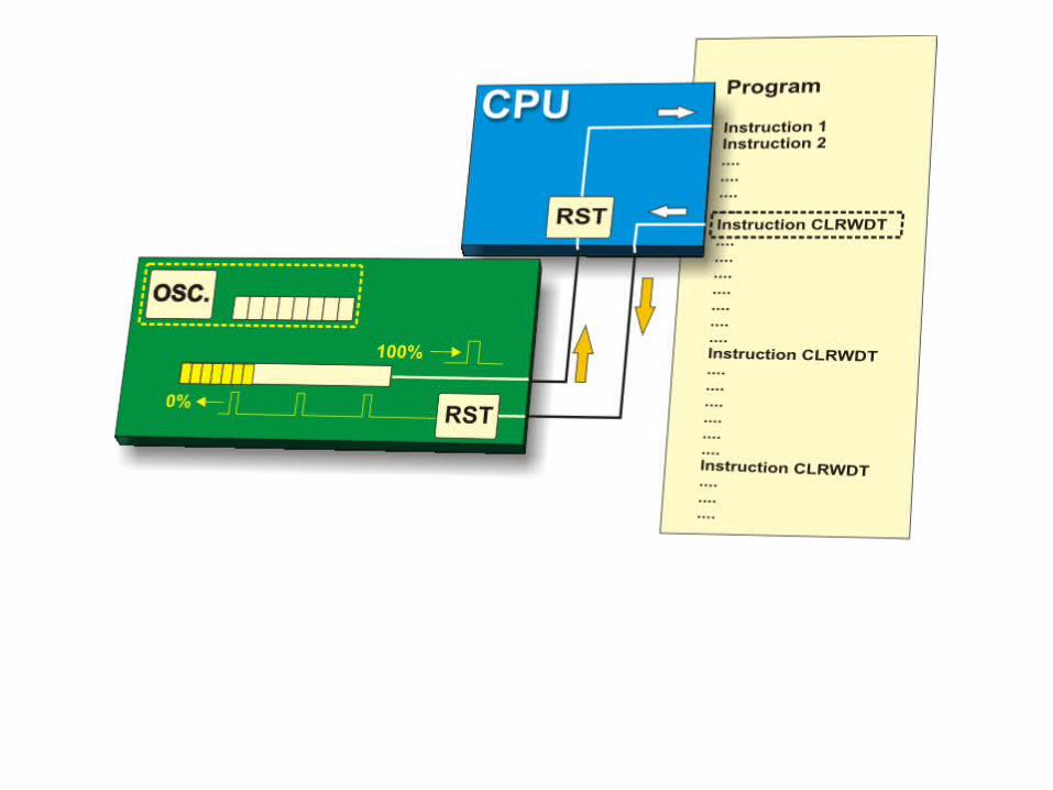
Watchdog Timer
The Watchdog Timer is a timer connected to a completely separate RC oscillator within the microcontroller.
If the watchdog timer is enabled, every time it counts up to the program end, the microcontroller reset occurs and program execution starts from the first instruction. The point is to prevent this from happening by using a specific command. The whole idea is based on the fact that every program is executed in several longer or shorter loops.
If instructions which reset the watchdog timer are set at the appropriate program locations, besides commands being regularly executed, then the operation of the watchdog timer will not affect program execution. If for any reason (usually electrical noises in industry), the program counter “gets stuck” on some memory location from which there is no return, the watchdog will not be cleared and the register’s value being constantly incremented will reach the maximum et voila! Reset occurs!
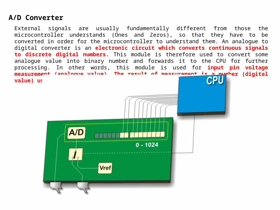
A/D Converter
External signals are usually fundamentally different from those the microcontroller understands (Ones and Zeros), so that they have to be converted in order for the microcontroller to understand them. An analogue to digital converter is an electronic circuit which converts continuous signals to discrete digital numbers. This module is therefore used to convert some analogue value into binary number and forwards it to the CPU for further processing. In other words, this module is used for input pin voltage measurement (analogue value). The result of measurement is a number (digital value) used and processed later in the program.
Central Processor Unit (CPU)
RISC Reduced Instruction Set Computer, gives the PIC16C7x two great advantages:
•The CPU can recognizes only 35 simple instructions (In order to program some other microcontrollers it is necessary to know more than 200 instructions by heart).
•The execution time is the same for all instructions except two and lasts 4 clock cycles (oscillator frequency is stabilized by a quartz crystal). The Jump and Branch instructions execution time is 2 clock cycles. It means that if the microcontroller’s operating speed is 20MHz, execution time of each instruction will be 200nS, i.e. the program will be executed at the speed of 5 million instructions per second!
Memory
This microcontroller has three types of memory- ROM, RAM and EEPROM. All of them will be separately discussed since each has specific functions, features and organization.
ROM Memory
ROM memory is used to permanently save the program being executed. This is why it is often called “program memory”. The PIC16C7X has 8Kb of ROM (in total of 8192 locations=8*1024). Since this ROM is made with FLASH technology, its contents can be changed by providing a special programming voltage (13V).
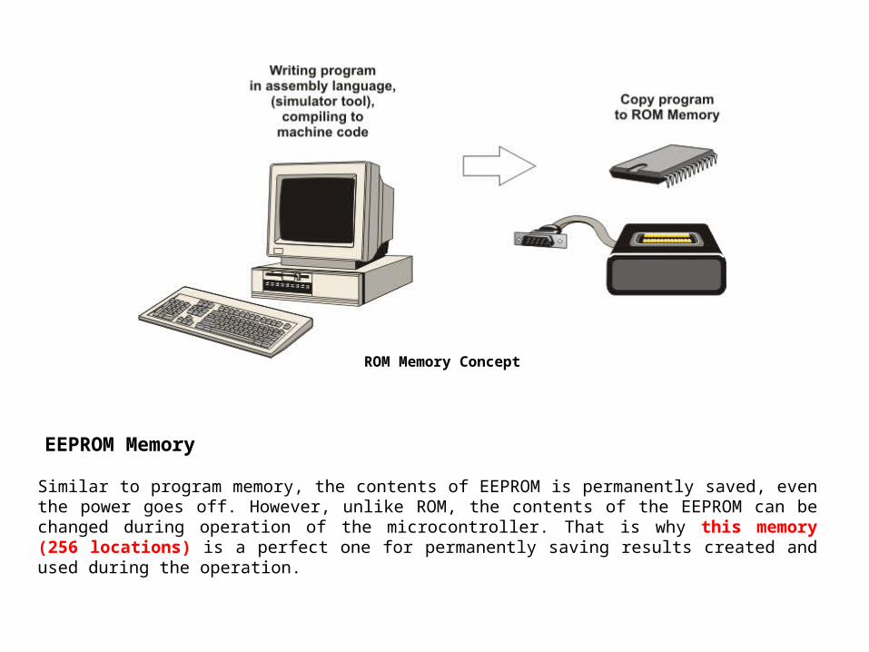
ROM Memory Concept
Similar to program memory, the contents of EEPROM is permanently saved, even the power goes off. However, unlike ROM, the contents of the EEPROM can be changed during operation of the microcontroller. That is why this memory (256 locations) is a perfect one for permanently saving results created and used during the operation.
EEPROM Memory
This is the third and the most complex part of microcontroller memory. In this case, it consists of two parts: general-purpose registers and special-function registers (SFR).
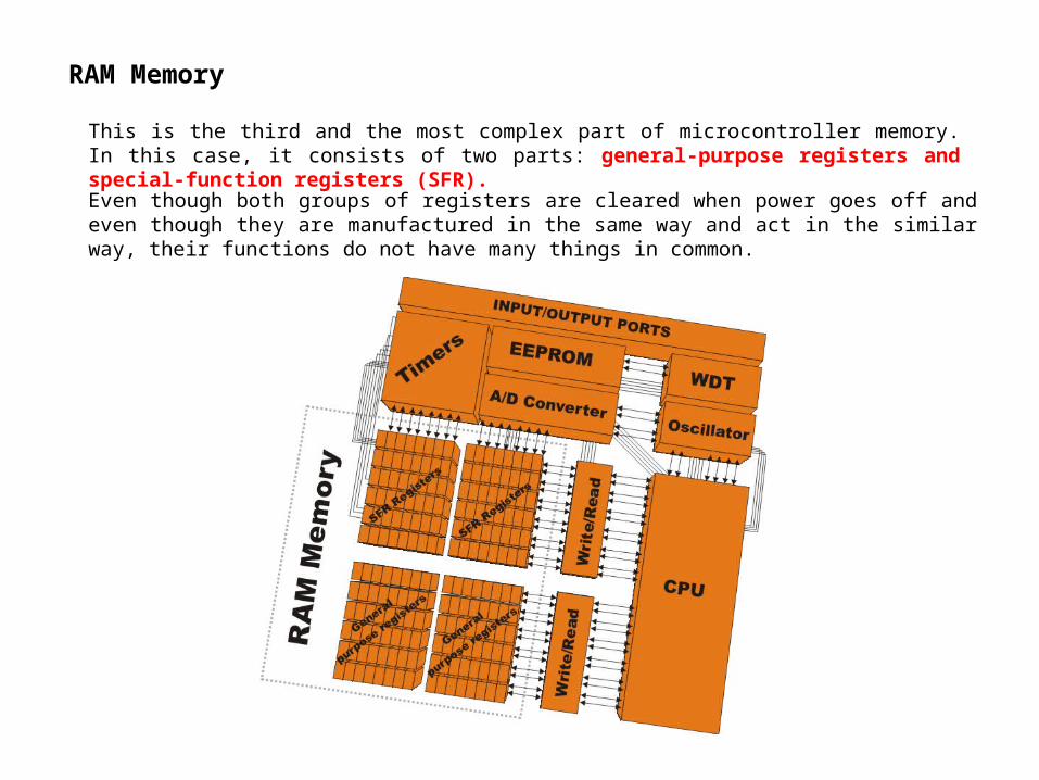
RAM Memory
Even though both groups of registers are cleared when power goes off and even though they are manufactured in the same way and act in the similar way, their functions do not have many things in common.

General-Purpose Registers
General-Purpose registers are used for storing temporary data and results created during operation. For example, if the program performs a counting (for example, counting products on the assembly line), it is necessary to have a register which stands for what we in everyday life call “sum”. Since the microcontroller is not creative at all, it is necessary to specify the address of some general purpose register and assign it a new function. A simple program to increment the value of this register by 1, after each product passes through a sensor, should be created.
Therefore, the microcontroller can execute that program because it now knows what and where the sum which must be incremented is. Similarly to this simple example, each program variable must be pre assigned some of general-purpose register.
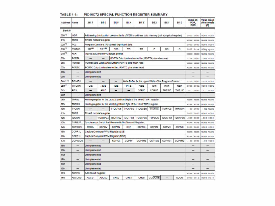
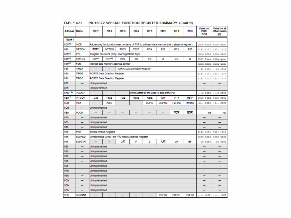
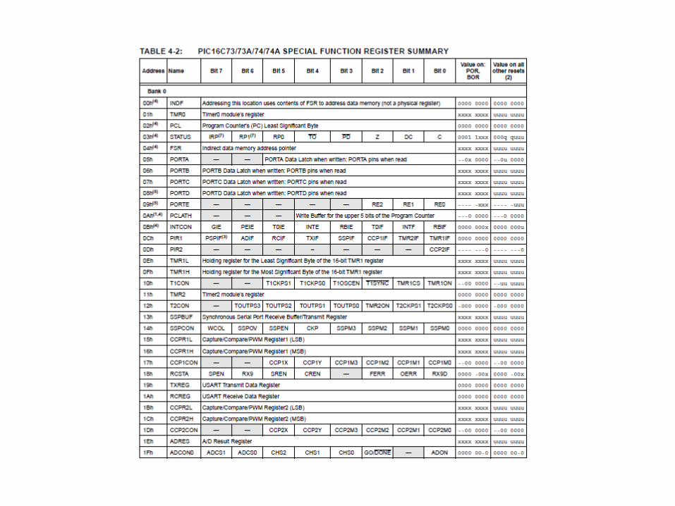
SFR Registers
Special-Function registers are also RAM memory locations, but unlike general-purpose registers, their purpose is predetermined during manufacturing process and cannot be changed. Since their bits are physically connected to particular circuits on the chip (A/D converter, serial communication module, etc.), any change of their contents directly affects the operation of the microcontroller or some of its circuits. For example, by changing the TRISA register, the function of each port A pin can be changed in a way it acts as input or output. Another feature of these memory locations is that they have their names (registers and their bits), which considerably facilitates program writing. Since high-level programming language can use the list of all registers with their exact addresses, it is enough to specify the register’s name in order to read or change its contents.
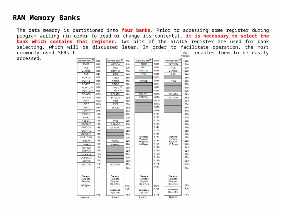
RAM Memory Banks
The data memory is partitioned into four banks. Prior to accessing some register during program writing (in order to read or change its contents), it is necessary to select the bank which contains that register. Two bits of the STATUS register are used for bank selecting, which will be discussed later. In order to facilitate operation, the most commonly used SFRs have the same address in all banks which enables them to be easily accessed.
STACK
•A part of the RAM used for the stack consists of eight 13-bit registers. Before the microcontroller starts to execute a subroutine (CALL instruction) or when an interrupt occurs, the address of first next instruction being currently executed is pushed onto the stack, i.e. onto one of its registers. In that way, upon subroutine or interrupt execution, the microcontroller knows from where to continue regular program execution. This address is cleared upon return to the main program because there is no need to save it any longer, and one location of the stack is automatically available for further use.
•It is important to understand that data is always circularly pushed onto the stack. It means that after the stack has been pushed eight times, the ninth push overwrites the value that was stored with the first push. The tenth push overwrites the second push and so on. Data overwritten in this way is not recoverable. In addition, the programmer cannot access these registers for write or read and there is no Status bit to indicate stack overflow or stack underflow conditions. For that reason, one should take special care of it during program writing.
Interrupt System
The first thing that the microcontroller does when an interrupt request arrives is to execute the current instruction and then stop regular program execution. Immediately after that, the current program memory address is automatically pushed onto the stack and the default address (predefined by the manufacturer) is written to the program counter. That location from where the program continues execution is called the interrupt vector. For the PIC16C7X microcontroller, this address is 0004h. As seen in Fig. 1-7 below, the location containing interrupt vector is passed over during regular program execution.
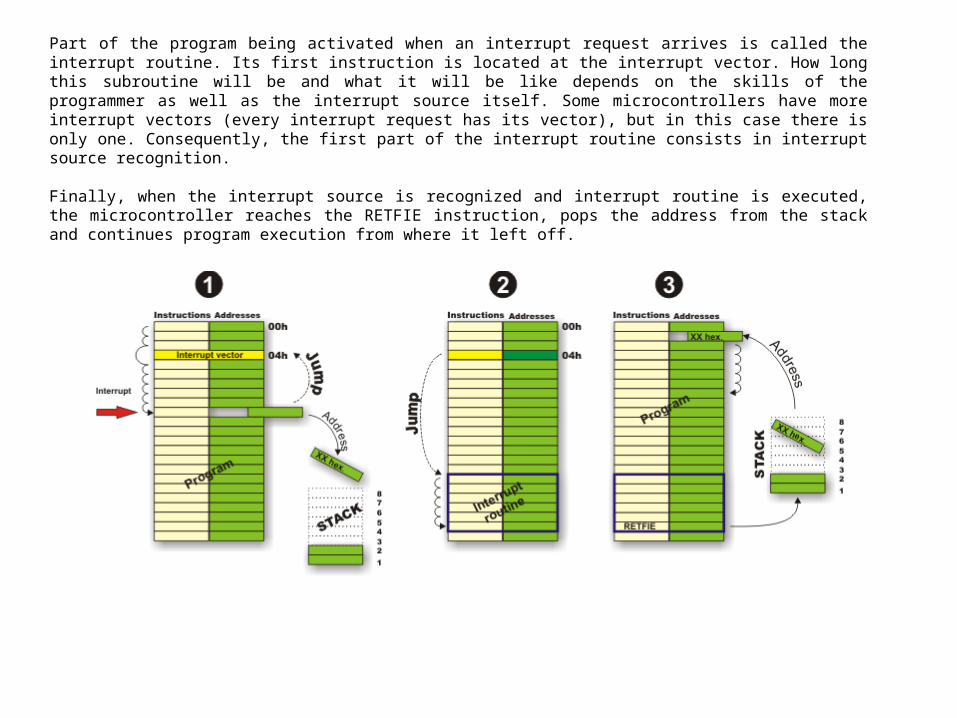
Part of the program being activated when an interrupt request arrives is called the interrupt routine. Its first instruction is located at the interrupt vector. How long this subroutine will be and what it will be like depends on the skills of the programmer as well as the interrupt source itself. Some microcontrollers have more interrupt vectors (every interrupt request has its vector), but in this case there is only one. Consequently, the first part of the interrupt routine consists in interrupt source recognition.
Finally, when the interrupt source is recognized and interrupt routine is executed, the microcontroller reaches the RETFIE instruction, pops the address from the stack and continues program execution from where it left off.

The special function registers can be classified into two categories:
• Core (CPU) registers - control and monitor operation and processes in the central processor. Even though there are only a few of them, the operation of the whole microcontroller depends on their contents.• Peripheral SFRs- control the operation of peripheral units (serial communication module, A/D converter etc.). Each of these registers is mainly specialized for one circuit and for that reason they will be described along with the circuit they are in control of.
The core (CPU) registers of the PIC16C7X microcontroller are described here. Since their bits control several different circuits within the chip, it is not possible to classify them into some special group. These bits are described along with the processes they control.
STATUS Register

The STATUS register contains: the arithmetic status of the W register, the RESET status and the bank select bits for data memory. One should be careful when writing a value to this register because if you do it wrong, the results may be different than expected. For example, if you try to clear all bits using the CLRF STATUS instruction, the result in the register will be 000xx1xx instead of the expected 00000000. Such errors occur because some of the bits of this register are set or cleared according to the hardware as well as because the bits 3 and 4 are readable only. For these reasons, if it is required to change its content (for example, to change active bank), it is recommended to use only instructions which do not affect any Status bits (C, DC and Z).
•IRP - Bit selects register bank. It is used for indirect addressing. •1 - Banks 0 and 1 are active (memory location 00h-FFh) •0 - Banks 2 and 3 are active (memory location 100h-1FFh)
RP1,RP0 - Bits select register bank. They are used for direct addressing.
RP1 RP0 Active Bank
0 0 Bank0
0 1 Bank1
1 0 Bank2
1 1 Bank3
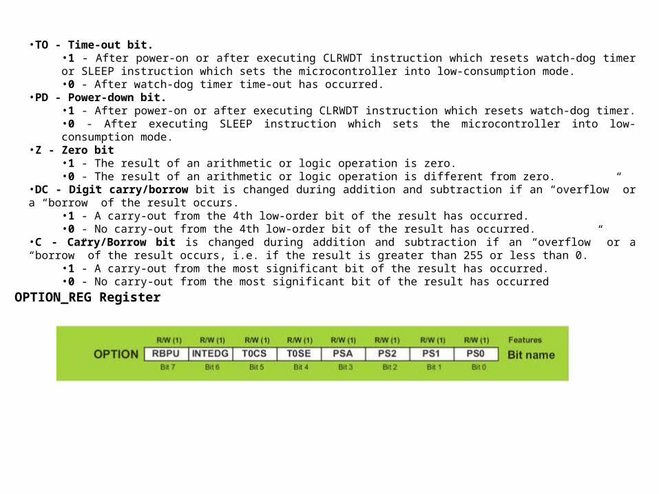
•TO - Time-out bit. •1 - After power-on or after executing CLRWDT instruction which resets watch-dog timer or SLEEP instruction which sets the microcontroller into low-consumption mode. •0 - After watch-dog timer time-out has occurred.
•PD - Power-down bit. •1 - After power-on or after executing CLRWDT instruction which resets watch-dog timer. •0 - After executing SLEEP instruction which sets the microcontroller into low-consumption mode.
•Z - Zero bit •1 - The result of an arithmetic or logic operation is zero. •0 - The result of an arithmetic or logic operation is different from zero.
•DC - Digit carry/borrow bit is changed during addition and subtraction if an “overflow” or a “borrow” of the result occurs. •1 - A carry-out from the 4th low-order bit of the result has occurred. •0 - No carry-out from the 4th low-order bit of the result has occurred.
•C - Carry/Borrow bit is changed during addition and subtraction if an “overflow” or a “borrow” of the result occurs, i.e. if the result is greater than 255 or less than 0.
•1 - A carry-out from the most significant bit of the result has occurred. •0 - No carry-out from the most significant bit of the result has occurred
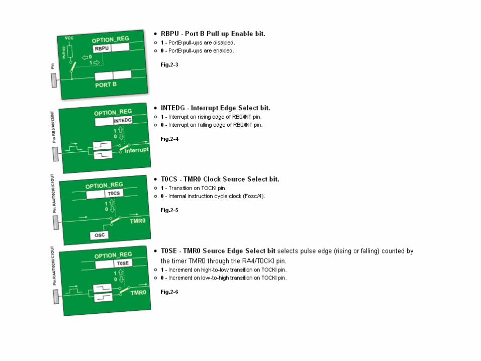
OPTION_REG Register

Interrupt System Registers
When an interrupt request arrives it does not mean that interrupt will automatically occur, because it must also be enabled by the user (from within the program). Because of that, there are special bits used to enable or disable interrupts. It is easy to recognize these bits by IE contained in their names (stands for Interrupt Enable). Besides, each interrupt is associated with another bit called the flag which indicates that interrupt request has arrived regardless of whether it is enabled or not. They are also easily recognizable by the last two letters contained in their names- IF (Interrupt Flag).
If the appropriate IE bit is not set (0), this event will be completely ignored. Otherwise, an interrupt occurs! In case several interrupt sources are enabled, it is necessary to detect the active one before the interrupt routine starts execution. Source detection is performed by checking flag bits.
•GIE bit - enables all unmasked interrupts and disables all interrupts simultaneously.•PEIE bit - enables all unmasked peripheral interrupts and disables all peripheral interrupts (This does not concern Timer TMR0 and port B interrupt sources).
To enable interrupt caused by changing logic state on port B, it is necessary to enable it for each bit separately. In this case, bits of the IOCB register have the function to control IE bits.


INTCON Register
The INTCON register contains various enable and flag bits for TMR0 register overflow, PORTB change and external INT pin interrupts.
GIE - Global Interrupt Enable bit - controls all possible interrupt sources simultaneously. 1 - Enables all unmasked interrupts.0 - Disables all interrupts.
PEIE - Peripheral Interrupt Enable bit acts similar to GIE, but controls interrupts enabled by peripherals. It means that it does not affect interrupts triggered by the timer TMR0 or by changing state on port B or RB0/INT pin.
1 - Enables all unmasked peripheral interrupts.0 - Disables all peripheral interrupts.
T0IE - TMR0 Overflow Interrupt Enable bit controls interrupt enabled by TMR0 overflow. 1 - Enables the TMR0 interrupt.0 - Disables the TMR0 interrupt.
INTE - RB0/INT External Interrupt Enable bit controls interrupt caused by changing logic state on pin RB0/IN (external interrupt). 1 - Enables the INT external interrupt.0 - Disables the INT external interrupt.
RBIE - RB Port Change Interrupt Enable bit. When configured as inputs, port B pins may cause interrupt by changing their logic state (no matter whether it is highto- low transition or vice versa, fact that something is changed only matters). This bit determines whether interrupt is to occur or not.
1 - Enables the port B change interrupt.0 - Disables the port B change interrupt.
T0IF - TMR0 Overflow Interrupt Flag bit registers the timer TMR0 register overflow, when counting starts from zero. 1 - TMR0 register has overflowed (bit must be cleared in software).0 - TMR0 register has not overflowed.
INTF - RB0/INT External Interrupt Flag bit registers change of logic state on the RB0/INT pin. 1 - The INT external interrupt has occurred (must be cleared in software).0 - The INT external interrupt has not occurred.
RBIF - RB Port Change Interrupt Flag bit registers change of logic state of some port B input pins. 1 - At least one of the port B general purpose I/O pins has changed state. Upon reading portB, RBIF (flag bit) must be cleared in software.0 - None of the port B general purpose I/O pins has changed state.

PIE1 Register The PIE1 register contains the peripheral interrupt enable bits.
ADIE - A/D Converter Interrupt Enable bit. 1 - Enables the ADC interrupt.0 - Disables the ADC interrupt.
RCIE - EUSART Receive Interrupt Enable bit. 1 - Enables the EUSART receive interrupt.0 - Disables the EUSART receive interrupt.
TXIE - EUSART Transmit Interrupt Enable bit. 1 - Enables the EUSART transmit interrupt.0 - Disables the EUSART transmit interrupt.
SSPIE - Master Synchronous Serial Port (MSSP) Interrupt Enable bit - enables an interrupt request to be generated after each data transfer via synchronous serial communication module (SPI or I2C mode).
1 - Enables the MSSP interrupt.0 - Disables the MSSP interrupt.
CCP1IE - CCP1 Interrupt Enable bit enables an interrupt request to be generated in CCP1 module used for PWM signal processing.
1 - Enables the CCP1 interrupt.0 - Disables the CCP1 interrupt.
TMR2IE - TMR2 to PR2 Match Interrupt Enable bit 1 - Enables the TMR2 to PR2 match interrupt.0 - Disables the TMR2 to PR2 match interrupt.
TMR1IE - TMR1 Overflow Interrupt Enable bit enables an interrupt request to be generated after each timer TMR1 register overflow, i.e. when the counting starts from zero.
1 - Enables the TMR1 overflow interrupt.0 - Disables the TMR1 overflow interrupt.

PIE2 Register The PIE2 Register also contains the various interrupt enable bits.
OSFIE - Oscillator Fail Interrupt Enable bit. 1 - Enables oscillator fail interrupt.0 - Disables oscillator fail interrupt.
C2IE - Comparator C2 Interrupt Enable bit. 1 - Enables Comparator C2 interrupt.0 - Disables Comparator C2 interrupt.
C1IE - Comparator C1 Interrupt Enable bit. 1 - Enables Comparator C1 interrupt.0 - Disables Comparator C1 interrupt.
EEIE - EEPROM Write Operation Interrupt Enable bit. 1 - Enables EEPROM write operation interrupt.0 - Disables EEPROM write operation interrupt.
BCLIE - Bus Collision Interrupt Enable bit. 1 - Enables bus collision interrupt.0 - Disables bus collision interrupt.
ULPWUIE - Ultra Low-Power Wake-up Interrupt Enable bit. 1 - Enables Ultra Low-Power Wake-up interrupt.0 - Disables Ultra Low-Power Wake-up interrupt.
CCP2IE - CCP2 Interrupt Enable bit. 1 - Enables CCP2 interrupt.0 - Disables CCP2 interrupt.
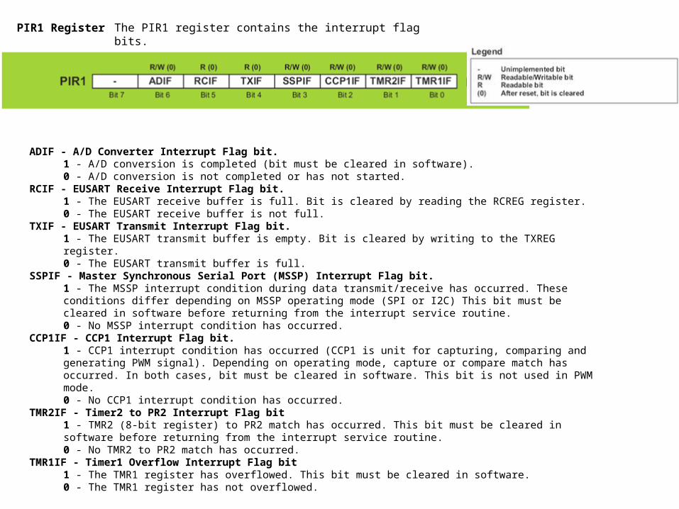
PIR1 Register The PIR1 register contains the interrupt flag bits.
ADIF - A/D Converter Interrupt Flag bit. 1 - A/D conversion is completed (bit must be cleared in software).0 - A/D conversion is not completed or has not started.
RCIF - EUSART Receive Interrupt Flag bit. 1 - The EUSART receive buffer is full. Bit is cleared by reading the RCREG register.0 - The EUSART receive buffer is not full.
TXIF - EUSART Transmit Interrupt Flag bit. 1 - The EUSART transmit buffer is empty. Bit is cleared by writing to the TXREG register.0 - The EUSART transmit buffer is full.
SSPIF - Master Synchronous Serial Port (MSSP) Interrupt Flag bit. 1 - The MSSP interrupt condition during data transmit/receive has occurred. These conditions differ depending on MSSP operating mode (SPI or I2C) This bit must be cleared in software before returning from the interrupt service routine.0 - No MSSP interrupt condition has occurred.
CCP1IF - CCP1 Interrupt Flag bit. 1 - CCP1 interrupt condition has occurred (CCP1 is unit for capturing, comparing and generating PWM signal). Depending on operating mode, capture or compare match has occurred. In both cases, bit must be cleared in software. This bit is not used in PWM mode.0 - No CCP1 interrupt condition has occurred.
TMR2IF - Timer2 to PR2 Interrupt Flag bit 1 - TMR2 (8-bit register) to PR2 match has occurred. This bit must be cleared in software before returning from the interrupt service routine.0 - No TMR2 to PR2 match has occurred.
TMR1IF - Timer1 Overflow Interrupt Flag bit 1 - The TMR1 register has overflowed. This bit must be cleared in software.0 - The TMR1 register has not overflowed.
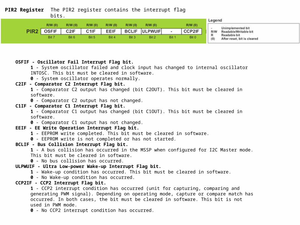
PIR2 Register The PIR2 register contains the interrupt flag bits.
OSFIF - Oscillator Fail Interrupt Flag bit. 1 - System oscillator failed and clock input has changed to internal oscillator INTOSC. This bit must be cleared in software.0 - System oscillator operates normally.
C2IF - Comparator C2 Interrupt Flag bit. 1 - Comparator C2 output has changed (bit C2OUT). This bit must be cleared in software.0 - Comparator C2 output has not changed.
C1IF - Comparator C1 Interrupt Flag bit. 1 - Comparator C1 output has changed (bit C1OUT). This bit must be cleared in software.0 - Comparator C1 output has not changed.
EEIF - EE Write Operation Interrupt Flag bit. 1 - EEPROM write completed. This bit must be cleared in software.0 - EEPROM write is not completed or has not started.
BCLIF - Bus Collision Interrupt Flag bit. 1 - A bus collision has occurred in the MSSP when configured for I2C Master mode. This bit must be cleared in software.0 - No bus collision has occurred.
ULPWUIF - Ultra Low-power Wake-up Interrupt Flag bit. 1 - Wake-up condition has occurred. This bit must be cleared in software.0 - No Wake-up condition has occurred.
CCP2IF - CCP2 Interrupt Flag bit. 1 - CCP2 interrupt condition has occurred (unit for capturing, comparing and generating PWM signal). Depending on operating mode, capture or compare match has occurred. In both cases, the bit must be cleared in software. This bit is not used in PWM mode.0 - No CCP2 interrupt condition has occurred.
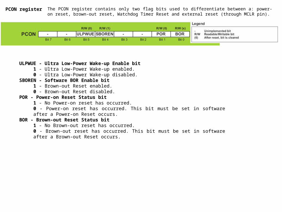
PCON register The PCON register contains only two flag bits used to differentiate between a: power-on reset, brown-out reset, Watchdog Timer Reset and external reset (through MCLR pin).
ULPWUE - Ultra Low-Power Wake-up Enable bit 1 - Ultra Low-Power Wake-up enabled.0 - Ultra Low-Power Wake-up disabled.
SBOREN - Software BOR Enable bit 1 - Brown-out Reset enabled.0 - Brown-out Reset disabled.
POR - Power-on Reset Status bit 1 - No Power-on reset has occurred.0 - Power-on reset has occurred. This bit must be set in software after a Power-on Reset occurs.
BOR - Brown-out Reset Status bit 1 - No Brown-out reset has occurred.0 - Brown-out reset has occurred. This bit must be set in software after a Brown-out Reset occurs.