Space engineering - ESCIES
219
ECSS-E-HB-20-05A 12 December 2012 Space engineering High voltage engineering and design handbook ECSS Secretariat ESA-ESTEC Requirements & Standards Division Noordwijk, The Netherlands ECSS Secretariat ESA-ESTEC Requirements & Standards Division Noordwijk, The Netherlands ECSS Secretariat ESA-ESTEC Requirements & Standards Division Noordwijk, The Netherlands ECSS Secretariat ESA-ESTEC Requirements & Standards Division Noordwijk, The Netherlands ECSS Secretariat ESA-ESTEC Requirements & Standards Division Noordwijk, The Netherlands ECSS Secretariat ESA-ESTEC Requirements & Standards Division Noordwijk, The Netherlands ECSS Secretariat ESA-ESTEC Requirements & Standards Division Noordwijk, The Netherlands ECSS Secretariat ESA-ESTEC Requirements & Standards Division Noordwijk, The Netherlands ECSS Secretariat ESA-ESTEC Requirements & Standards Division Noordwijk, The Netherlands ECSS Secretariat ESA-ESTEC Requirements & Standards Division Noordwijk, The Netherlands ECSS Secretariat ESA-ESTEC Requirements & Standards Division Noordwijk, The Netherlands ECSS Secretariat ESA-ESTEC Requirements & Standards Division Noordwijk, The Netherlands
Transcript of Space engineering - ESCIES
ECSS-E-HB-20-05A 12 December 2012
Space engineering High voltage engineering and design handbook
ECSS Secretariat ESA-ESTEC
Requirements & Standards Division Noordwijk, The Netherlands
ECSS Secretariat ESA-ESTEC
Requirements & Standards Division Noordwijk, The Netherlands
ECSS Secretariat ESA-ESTEC
Requirements & Standards Division Noordwijk, The Netherlands
ECSS Secretariat ESA-ESTEC
Requirements & Standards Division Noordwijk, The Netherlands
ECSS Secretariat ESA-ESTEC
Requirements & Standards Division Noordwijk, The Netherlands
ECSS Secretariat ESA-ESTEC
Requirements & Standards Division Noordwijk, The Netherlands
ECSS Secretariat ESA-ESTEC
Requirements & Standards Division Noordwijk, The Netherlands
ECSS Secretariat ESA-ESTEC
Requirements & Standards Division Noordwijk, The Netherlands
ECSS Secretariat ESA-ESTEC
Requirements & Standards Division Noordwijk, The Netherlands
ECSS Secretariat ESA-ESTEC
Requirements & Standards Division Noordwijk, The Netherlands
ECSS Secretariat ESA-ESTEC
Requirements & Standards Division Noordwijk, The Netherlands
ECSS Secretariat ESA-ESTEC
Requirements & Standards Division Noordwijk, The Netherlands
ECSS‐E‐HB‐20‐05A
12 December 2012
2
Foreword
This Handbook is one document of the series of ECSS Documents intended to be used as supporting
material for ECSS Standards in space projects and applications. ECSS is a cooperative effort of the
European Space Agency, national space agencies and European industry associations for the purpose
of developing and maintaining common standards.
The material in this Handbook is defined in terms of description and recommendation how to
organize and perform the work of design, manufacture, integrate and test high voltage equipment,
modules and components for use in space applications. It complements ECSS‐E‐ST‐20C and covers
power conditioning elements as well as their interfaces to the power consumers.
This handbook has been prepared by the ECSS‐E‐HB‐20‐05A Working Group, reviewed by the ECSS
Executive Secretariat and approved by the ECSS Technical Authority.
Disclaimer
ECSS does not provide any warranty whatsoever, whether expressed, implied, or statutory, including,
but not limited to, any warranty of merchantability or fitness for a particular purpose or any warranty
that the contents of the item are error‐free. In no respect shall ECSS incur any liability for any
damages, including, but not limited to, direct, indirect, special, or consequential damages arising out
of, resulting from, or in any way connected to the use of this document, whether or not based upon
warranty, business agreement, tort, or otherwise; whether or not injury was sustained by persons or
property or otherwise; and whether or not loss was sustained from, or arose out of, the results of, the
item, or any services that may be provided by ECSS.
Published by: ESA Requirements and Standards Division
ESTEC, P.O. Box 299,
2200 AG Noordwijk
The Netherlands
Copyright: 2012© by the European Space Agency for the members of ECSS

ECSS‐E‐HB‐20‐05A
12 December 2012
3
Change log
ECSS‐E‐HB‐20‐05A
12 December 2012
First issue
ECSS‐E‐HB‐20‐05A
12 December 2012
4
Table of contents
Foreword .................................................................................................................... 2
Change log ................................................................................................................. 3
Introduction .............................................................................................................. 12
1 Scope ..................................................................................................................... 14
2 References ............................................................................................................ 15
3 Terms, definitions and abbreviated terms .......................................................... 18
3.1 Terms from other documents ................................................................................... 18
3.2 Terms specific to the present document .................................................................. 19
3.3 Abbreviated terms .................................................................................................... 22
4 High voltage design considerations ................................................................... 24
4.1 Environment ............................................................................................................. 24
4.1.1 Impact of environment ................................................................................ 24
4.1.2 Pressure ..................................................................................................... 25
4.1.3 Temperature ............................................................................................... 27
4.1.4 Energetic Particle Radiation ....................................................................... 28
4.1.5 Space Debris and Micrometeoroids ........................................................... 28
4.1.6 Plasma ........................................................................................................ 29
4.1.7 Mechanical ................................................................................................. 29
4.2 Electrical insulation ................................................................................................... 30
4.2.1 Categories of insulation .............................................................................. 30
4.2.2 Gaseous insulation ..................................................................................... 30
4.2.3 Liquid insulation .......................................................................................... 33
4.2.4 Solid insulation ........................................................................................... 34
4.2.5 Vacuum insulation ...................................................................................... 37
4.2.6 Composites ................................................................................................. 38
4.3 Life limiting factors .................................................................................................... 38
4.3.1 Perspective ................................................................................................. 38
4.3.2 Electrical breakdown .................................................................................. 39
ECSS‐E‐HB‐20‐05A
12 December 2012
5
4.3.3 Partial discharges ....................................................................................... 45
4.3.4 Paschen breakdown ................................................................................... 48
4.3.5 Ageing ........................................................................................................ 50
4.4 Typical applications .................................................................................................. 56
4.4.1 DC-DC High voltage power conditioners .................................................... 56
4.4.2 Electronic power conditioners for TWTA .................................................... 58
4.4.3 Electric propulsion ...................................................................................... 65
4.4.4 Microwave tubes ......................................................................................... 72
4.4.5 Scientific instruments and experiments ...................................................... 75
5 High voltage design principles ............................................................................ 77
5.1 Basic design principles ............................................................................................. 77
5.1.1 Control of voltage ....................................................................................... 77
5.1.2 Control of electrical field strengths ............................................................. 79
5.1.3 Control of electrical field distribution ........................................................... 89
5.1.4 Control of insulation properties ................................................................... 91
5.1.5 Control of surface properties ...................................................................... 94
5.1.6 Control of partial discharges ....................................................................... 96
5.1.7 Control of corona effects ............................................................................ 97
5.1.8 Control of Paschen breakdown .................................................................. 98
5.1.9 Control of triple junction effects ................................................................ 100
5.1.10 Control of creepage path .......................................................................... 101
5.1.11 Control of surface charging ...................................................................... 102
5.1.12 Control of interferences ............................................................................ 104
5.2 High voltage assemblies ........................................................................................ 107
5.2.1 Solid insulation: potted modules ............................................................... 107
5.2.2 Solid insulation: others ............................................................................. 127
5.2.3 Gaseous insulation ................................................................................... 129
5.2.4 Liquid insulation (Oil) ................................................................................ 134
5.2.5 Space vacuum insulation .......................................................................... 135
5.3 High voltage components ....................................................................................... 143
5.3.1 Transformers and inductors ...................................................................... 143
5.3.2 Capacitors ................................................................................................ 146
5.3.3 Resistors ................................................................................................... 149
5.3.4 Semiconductors ........................................................................................ 151
5.3.5 Wires and cables ...................................................................................... 151
5.3.6 Connectors ............................................................................................... 156
5.3.7 Interconnections ....................................................................................... 157
ECSS‐E‐HB‐20‐05A
12 December 2012
6
5.3.8 Insulators and spacers ............................................................................. 159
5.3.9 Feedthroughs ........................................................................................... 160
5.3.10 Printed circuit boards ................................................................................ 161
5.3.11 Other components .................................................................................... 163
6 High voltage testing ........................................................................................... 164
6.1 Non-Destructive Testing ......................................................................................... 164
6.1.1 Insulation Resistance Test (INR) .............................................................. 164
6.1.2 Bulk Resistance Measurement (BRM) ..................................................... 165
6.1.3 Surface Resistance Measurement (SRM) ................................................ 166
6.1.4 Polarisation and Depolarisation Current Measurement (PDC) ................. 167
6.1.5 Dielectric Loss Factor Test (DLF) ............................................................. 168
6.1.6 Partial Discharge Test (PDT) .................................................................... 169
6.1.7 Dielectric Withstanding Voltage Test (DWV) ............................................ 175
6.1.8 Triple Junction Test (TRJ) ........................................................................ 177
6.1.9 Critical pressure testing/Corona testing (CPT) ......................................... 179
6.1.10 Life testing (LIT) ........................................................................................ 182
6.1.11 Accelerated life testing (ALT) ................................................................... 183
6.1.12 Burn-in testing (BIT) ................................................................................. 184
6.2 Destructive Testing ................................................................................................. 185
6.2.1 Breakdown Voltage Test (BVT) ................................................................ 185
6.2.2 Lifetime evaluation testing (LET) .............................................................. 186
6.3 Supplementary Methods ........................................................................................ 187
6.4 Testing strategy ...................................................................................................... 188
7 High voltage product aspects ........................................................................... 190
7.1.1 Best practice for materials and processes selection ................................ 190
7.1.2 Best practice for design ............................................................................ 192
7.1.3 Best practice for qualification .................................................................... 194
7.1.4 Best practice for flight acceptance ............................................................ 196
7.1.5 Best practice for verification ..................................................................... 197
7.1.6 PID ............................................................................................................ 198
7.1.7 Evaluation Plan ......................................................................................... 198
8 Specific problem areas ...................................................................................... 199
8.1.1 High voltage converters ............................................................................ 199
8.1.2 Electric propulsion .................................................................................... 201
8.1.3 Electron devices (tubes) ........................................................................... 206
8.1.4 Scientific instruments and experiments .................................................... 206
ECSS‐E‐HB‐20‐05A
12 December 2012
7
8.1.5 EMC aspects ............................................................................................ 206
9 Hazards and safety ............................................................................................. 208
9.1 Hazards .................................................................................................................. 208
9.2 Safety ..................................................................................................................... 208
Annex A High Voltage Field Calculation Tables ................................................. 209
A.1 Principles of field efficiency factors for spheres and cylindrical geometries ........... 209
A.2 Spherical geometries .............................................................................................. 210
A.3 Cylindrical geometries ............................................................................................ 211
Annex B Best Practice References ...................................................................... 213
B.1 High Voltage Evaluation Plan ................................................................................. 213
B.1.1 Evaluation Activities .................................................................................. 213
B.1.2 Evaluation Plan ......................................................................................... 213
B.1.3 Manufacturing of Evaluation Samples ...................................................... 214
B.1.4 Test and Characterisation ........................................................................ 214
B.1.5 Evaluation Review .................................................................................... 214
B.2 Materials Evaluation ............................................................................................... 215
B.3 PID – Process Identification Document .................................................................. 219
Figures
Figure 4-1: Arc Caused by Particle Bridge ............................................................................. 29
Figure 4-2: Discharge (breakdown) development in a gas volume between two electrodes by electron avalanche process ........................................................ 40
Figure 4-3: Electrical strengths of a liquid insulation (here: transformer oil in 2,5 mm gap) in relation to voltage exposure time and assumed breakdown mechanism ........................................................................................................ 42
Figure 4-4: Vacuum breakdown phenomena ......................................................................... 44
Figure 4-5: Typical partial discharge configurations ............................................................... 46
Figure 4-6: Electrical model of partial discharges for a gas-bubble in a solid ........................ 47
Figure 4-7: Breakdown voltage of gases vs. the product of pressure times gap spacing ...... 49
Figure 4-8: Electrical treeing caused by partial discharges .................................................... 52
Figure 4-9: Example: Fatigue (thermo-mechanical stress-related) failures in assemblies expressed as stress (∆T – temperature cycle amplitude) over number of thermal cycles.................................................................................................... 53
Figure 4-10: Example: Fatigue (thermo-mechanical stress-related) failures in assemblies expressed as stress (∆T – temperature cycle amplitude) over number of thermal cycles .................................................................................. 54
Figure 4-11: Electrical field strengths over time curve according to the Crine model ............ 56
Figure 4-12: DC/DC power conversion chains for high voltage of an EPC ............................ 57
ECSS‐E‐HB‐20‐05A
12 December 2012
8
Figure 4-13: Topologies of electronic power conditioners ...................................................... 58
Figure 4-14: Functional block diagram of an EPC .................................................................. 59
Figure 4-15: Example for a high voltage generation of an EPC ............................................. 61
Figure 4-16: Example of a high voltage transformer for an EPC ............................................ 62
Figure 4-17: Example of a FEM calculation result: Equipotential Lines for a Plane-to-Plane configuration with spherical edges of the upper plane ............................ 64
Figure 4-18: Principle of Electrical Propulsion vs. Chemical Propulsion ................................ 65
Figure 4-19: FEEP Ion Emitter Principle ................................................................................ 67
Figure 4-20: FEEP Ion Emitter Load – Equivalent Circuit ...................................................... 67
Figure 4-21: Hall Effect Thruster Principle ............................................................................. 68
Figure 4-22: HEMP Thruster Principle ................................................................................... 69
Figure 4-23: Ion Thruster Principle (Kaufmann) ..................................................................... 70
Figure 4-24: Radio Frequency Ion Thruster (RIT) Principle ................................................... 72
Figure 4-25: Schematic layout of a TWT ................................................................................ 73
Figure 4-26: Principle of the electron gun of a TWT ............................................................... 74
Figure 4-27: Principle of the collector stage of a TWT ........................................................... 74
Figure 5-1: Electrical field strength depending on voltage and geometrical parameters (Examples) ........................................................................................................ 81
Figure 5-2: Uniform electrical field for indefinite parallel planes ............................................. 81
Figure 5-3: Sphere-inside-sphere electrical field .................................................................... 82
Figure 5-4: Examples for practical use of field equations for spheres .................................... 84
Figure 5-5: Examples for practical: connections of wires by using spherical solder joints ..... 84
Figure 5-6: Cylinder-inside-cylinder electrical field ................................................................. 85
Figure 5-7: Space charge formation on an isolating surface .................................................. 86
Figure 5-8: Space charge formation on sharp-edged structures in various environments ..... 87
Figure 5-9: Surface charging of an isolator ............................................................................ 88
Figure 5-10: Correct meshing of shapes ................................................................................ 89
Figure 5-11: General: E-Field and voltage for a three-dimensional path ............................... 89
Figure 5-12: E-Field and voltage for gap lengths (straight path) ............................................ 90
Figure 5-13: Control of electrical field distribution - Examples ............................................... 91
Figure 5-14: Avoiding fibre bridging effect in liquid insulation ................................................ 92
Figure 5-15: Optimum design of interfaces between materials w.r.t. the electrical field ........ 94
Figure 5-16: Limit critical Paschen breakdown pressure range by limitation of maximum gap .................................................................................................................... 98
Figure 5-17: Paschen discharge in a gap between solid insulation and ground .................... 99
Figure 5-18: Triggered Paschen discharge in a gap between solid insulation and ground ............................................................................................................. 100
Figure 5-19: Critical triple-junction point/area in an interface between solid - gaseous/liquid/vacuum insulation - metal conductor ....................................... 100
ECSS‐E‐HB‐20‐05A
12 December 2012
9
Figure 5-20: Methods to reduce the influence of the triple junction zone by design ............... 101
Figure 5-21: Impact of creepage path on electrical field distribution .................................... 102
Figure 5-22: Designs to reduce impact of creepage path on electric insulation ................... 102
Figure 5-23: Designs to reduce impact of surface charging on electric insulation ............... 103
Figure 5-24: Segmenting of insulator to influence surface charging .................................... 104
Figure 5-25: Implementation of design measures minimizing interference problems for a typical high voltage power conditioner (regulated DC-DC converter for high voltage as an example)............................................................................ 106
Figure 5-26: Designs example: potting of embedded aluminium structure, i.e. an HV terminal ............................................................................................................ 112
Figure 5-27: Designs example: potting of embedded aluminium structure, i.e. HV terminal ............................................................................................................ 114
Figure 5-28: Shielding necessary to avoid exposure of an electronic part to excessive electrical field stress ........................................................................................ 115
Figure 5-29: Potting of PCB`s: typical design aspects ......................................................... 117
Figure 5-30: Transformer with rectifier and filter designed as two separate modules using open terminals for interconnecting HV harness ..................................... 119
Figure 5-31: Transformer and rectifier filter designed as two separate modules using potted terminals for interconnecting HV harness ............................................. 120
Figure 5-32: Transformer and rectifier filter designed as one combined module potted in (a) one or (b) two and more sequential potting processes .......................... 120
Figure 5-33: Designs example: Spherical solder ball ........................................................... 121
Figure 5-34: Fitting a potted assembly to partial discharge testing (Example of a potted transformer winding) ........................................................................................ 124
Figure 5-35: Examples for thermal drains embedded in potted modules ............................. 125
Figure 5-36: Relative Dielectric Strength of a SF6-N2-Mixture versus Composition of the Mixture ............................................................................................................. 131
Figure 5-37: Surface flashover process in a vacuum environment ...................................... 136
Figure 5-38: Surface shapes for insulators .......................................................................... 138
Figure 5-39: Arrangement of cylindrically layers of windings ............................................... 143
Figure 5-40: Arrangement of windings in discs of a bobbin ................................................. 145
Figure 5-41: Partial discharge test aspects of a high voltage transformer ........................... 146
Figure 5-42: Critical electrical field stress in the surrounding of high voltage capacitors and proposed measures .................................................................................. 148
Figure 5-43: Basic high voltage resistor design variants ...................................................... 149
Figure 5-44: High voltage resistor design aspects ............................................................... 150
Figure 5-45: Suitable partial discharge test setup for high voltage wires ............................. 152
Figure 5-46: Critical stress cases for high voltage wires ...................................................... 153
Figure 5-47: Critical stress cases for high voltage wires terminations ................................. 154
Figure 5-48: Interconnection of high voltage harness via soldering or crimping/bolting at terminals .......................................................................................................... 158
ECSS‐E‐HB‐20‐05A
12 December 2012
10
Figure 5-49: Flying lead interconnections ............................................................................ 159
Figure 5-50: Suitable insulator design variants .................................................................... 160
Figure 5-51: Suitable feedthrough design variants ............................................................... 161
Figure 6-1: Guard ring test set-up for bulk resistance measurement ................................... 165
Figure 6-2: Partial discharge test set-up .............................................................................. 171
Figure 6-3: Typical partial discharge test flow ...................................................................... 172
Figure 6-4: Partial discharge testing aspects. Example: High voltage transformer .............. 173
Figure 6-5: Dielectric Withstand Voltage Test Electrical Schematic ..................................... 176
Figure 6-6: Triple Junction Test Electrical Schematic .......................................................... 178
Figure 6-7: Critical Pressure Test Electrical Schematic ....................................................... 180
Figure 6-8: Breakdown Voltage Test Electrical Schematic .................................................. 185
Figure 8-1: High voltage conditioner with grounding at converter – load floating ................. 200
Figure 8-2: High voltage conditioner with grounding at load side – including a clamping device at the conditioner.................................................................................. 200
Figure 8-3: High voltage conditioner with grounding at load side – including a clamping device at the conditioner and triax HV cable for load connection .................... 201
Figure A-1 : Field efficiency factors (Schwaiger factors) η as a function of geometry parameter p for spheres .................................................................................. 210
Figure A-2 : Field efficiency factors (Schwaiger factors) η as a function of geometry parameter p for cylinders ................................................................................. 212
Figure A-3 : Field efficiency factors (Schwaiger factors) η as a function of geometry parameter p for cylinders ................................................................................. 212
Figure B-1 : Typical material evaluation flow ........................................................................ 217
Figure B-2 : Potted Rogowsky-profile electrodes ................................................................. 218
Figure B-3 : Crossed wire electrode ..................................................................................... 218
Figure B-4 : Material disk between electrodes ..................................................................... 218
Tables
Table 4-1: Course Classification of the potential impact to electrical insulations by environmental type ............................................................................................ 24
Table 4-2: Properties of gaseous insulations ......................................................................... 32
Table 4-3: Properties of liquid insulations .............................................................................. 33
Table 4-4: Properties of EP, PUR and SI ............................................................................... 35
Table 4-5: Properties of various polymers .............................................................................. 36
Table 4-6: Properties of porcelain and alumina ...................................................................... 37
Table 4-7: Paschen Minimum for various gases .................................................................... 50
Table 4-8: Overview on Electrical Propulsion Principles, Thruster Type and Electrical Physical Parameters .......................................................................................... 66
ECSS‐E‐HB‐20‐05A
12 December 2012
11
Table 5-1: Critical “thresholds” for high voltage ...................................................................... 78
Table 5-2: Orientation “map” for maximum electrical field strengths in electrical insulation ........................................................................................................... 80
Table 5-3: Orientation values (examples) for selection sphere structures to limit the maximum electrical field of a high voltage assembly ......................................... 84
Table 5-4: Dew point of SF6-N2-mixtures versus pressure and depending of composition ..................................................................................................... 132
Table 5-5: Surface shapes for insulators in combination with selected materials comparing the relative surface flashover strengths of +/- 45 degree cone insulators for various voltage waveforms w.r.t pure cylindrical shapes ........... 139
Table 5-6: Theoretical predictions and experimental consequences of methods to improve the surface flashover strengths in vacuum ........................................ 140
Table 5-7: Application matrix for PCB with high voltage ...................................................... 162
Table 6-1: Test methods, levels and acceptance criteria for partial discharge testing ......... 174
Table 6-2: Assessment of test methods w.r.t. its application ............................................... 188
Table 7-1: Typical material properties and reference test methods for high voltage insulation materials .......................................................................................... 191
Table 7-2: Best practice of verification for high voltage design aspects ............................... 197
Table A-1 : Sphere geometries ............................................................................................ 210
Table A-2 : Cylinder-parallel-to-a-cylinder geometries ......................................................... 211
Table A-3 : Cylinder-inside-a-cylinder geometries ............................................................... 211
Table B-1 : Product categories according to heritage (Ref.: ECSS-E-ST-10-02C) .............. 215
ECSS‐E‐HB‐20‐05A
12 December 2012
12
Introduction
The subject of high voltage engineering and design has been part of the spacecraft design process
since the early times of spaceflight.
This was due to need for high voltage power conditioners being a key element of communication
links. The relate expertise was built up in Europe in the decade of the 1980 with the support of the
development of modern Electronic Power Conditioners (EPC’s), to operate Travelling Wave Tube
Amplifiers for telecommunication satellites and for high power radar applications.
In 1989 ESA launched its first high power radar for earth observation onboard the ERS‐1 (European
Remote Sensing Satellite), achieving a technology for 15 kV – 17 kV in space.
Today typically between some ten and over hundred EPC’s with operating voltages of 5 kV ‐ 8 kV are
placed on many of the telecommunications satellites.
Several space borne radars with travelling wave tubes and klystrons are in orbit using voltage up to 20
kV. Various detectors for various kind of space environment with voltage between a few hundred
volts and up to 30 kV are used in many missions, high power lasers up to 150 kV were studied, and
even some experiments onboard the International Space Station using fancy high voltage sources.
The latest trend is the increasing use of electric propulsion for satellites dealing with supply voltage in
the range between a few hundred volts and above 10 kV. High voltage related anomalies have been
observed only a few times, some in the early years of building up experience, some also later,
especially when new developments were done with new teams inexperienced in the field.
A need was identified for a standard already in the early years of the space flight, the US air force and
NASA presented a series design and test handbook in the 1970’s and 1980’s. In Europe, ESA started
discussing a draft standard with industry: the PSS‐02‐303 draft 2 from 1992 “Requirements for High
Voltage Transformer and Components used in Electronic Power Conditioners for ESA Space Systems”
this became a quasi standard reference in many space projects, even if it was never formally released.
The growing diversity of high voltage application gave finally the urgency to make a new approach
for standardization. The discussion started in 2007 with ECSS who led to the conclusion, that a
standard would not satisfy the immediate needs for projects, as it would be too wide to cover the
diverse applications and also would not be suitable to transfer the “know‐how” of high voltage
engineering and design. Therefore it was decided to produce a handbook to give a broad scope of
knowledge and recommendations for design and test of high voltage equipment and components.
This document aims to satisfy these needs and provides a detailed view of high voltage knowledge
aspects as well as giving a guideline to identify suitable design rules.
Proper design of high voltage effects of these processes is part of the system engineering process as
defined in ECSS‐E‐ST‐20, where only a small subset of high voltage requirements is given.
For new projects involving high voltage equipment and design it is useful to provide this handbook as
a reference to generate suitable requirements specific to the targeted high voltage application.
Chapter 7 of this document gives some “best practice” statements.
ECSS‐E‐HB‐20‐05A
12 December 2012
13
Only a smart answer can be given to the definition of the range of voltages which should be
considered as high voltages: The ECSS‐E‐ST‐20C states for the definition of a high voltage “AC or DC
voltage at which partial discharges, corona, arcing or high electrical fields can occur”. For space
environment this can occur “. This in fact can already appear at 60 V – 80 V if a low pressure
environment in an inert gas provides a critical pressure for “Paschen Breakdown”. Under air (N2/O2
mixtures) this can occur for voltage of above 300 V.
ECSS‐E‐HB‐20‐05A
12 December 2012
14
1 Scope
This Handbook establishes guidelines to ensure a reliable design, manufacturing and testing of high
voltage electronic equipment and covers:
Design
Manufacturing
Verification/Testing
of equipment generating, carrying or consuming high voltage, like: high voltage power conditioner,
high voltage distribution (cables and connectors).
This Handbook is dedicated to all parties involved at all levels in the realization of space segment
hardware and its interface with high voltage for which ECSS‐E‐ST‐20C is applicable.
This handbook sets out to:
summarize most relevant aspects and data of high voltage insulation
provide design guidelines for high voltage insulation
provide design guidelines for high voltage electronic equipment
give an overview of appropriate high voltage test methods
establish a set of recommendations for generation design and verification rules and methods
provide best practices
Applicability is mainly focused on power conditioning equipment but may be also applicable for all
other high voltage electric and electronic power equipment used on space missions, except items of
experimental nature.
ECSS‐E‐HB‐20‐05A
12 December 2012
15
2 References
ECSS‐S‐ST‐00‐01C ECSS System – Glossary of terms
ECSS‐E‐ST‐10‐03C Space engineering ‐ Testing
ECSS‐E‐ST‐10‐02C Space engineering ‐ Verification
ECSS‐E‐ST‐10‐04C Space engineering ‐ Space environment
ECSS‐E‐ST‐20C Space engineering ‐ Electrical and electronic
ECSS‐E‐20‐01A Space engineering ‐ Multipaction design and test
ECSS‐E‐ST‐20‐06C Space engineering ‐ Spacecraft charging
ECSS‐E‐ST‐32C Space engineering ‐ Structural general requirements
ECSS‐Q‐ST‐30‐11C Space product assurance ‐ Derating – EEE components
ECSS‐Q‐ST‐70‐10C Space product assurance ‐ Qualification of printed circuit boards
ECSS‐Q‐ST‐70‐11C Space product assurance ‐ Procurement of printed circuit boards
ECSS‐Q‐70‐71A Space product assurance ‐ Data for selection of space materials and processes
ESA SP‐398
(May 1997)
Power supply and control unit (PCSU) for radio frequency ion thrusters (RIT)”
ESA, Proc. 2nd European Spacecraft Propulsion, Noordwijk, The Netherlands,
27‐29 May 1997 (ESA SP‐398), pp 643‐648.
ESA SP‐555
(June 2004)
The Power Control Unit for the Propulsion Engine of GOCE Program, Tato, C.;
Palencia, J.; De la Cruz, F., 4th International Spacecraft Propulsion Conference,
2‐4 June 2004 Chia Laguna (Cagliari), Sardinia, Italy
ESA SP‐569
(June 2004)
The T5 Ion Propulsion Assembly for Drag Compensation on GOCE,
Proceedings of the Second International GOCE User Workshop
AIAA 2005‐4224
(2005)
First Test Results of the 1 to 15 kW Coaxial HEMP 30250 Thurster, 41st
AIAA/ASME/SAE/ASEE Joint Propulsion Conference & Exhibit, 10 ‐ 13 July
2005, Tucson, Arizona
AIAA 2006‐4476
(2006)
High Power HEMP‐Thruster Module, Status and Results of a DLR and ESA
Development Program, 42nd AIAA/ASME/SAE/ASEE Joint Propulsion
Conference & Exhibit, 9 ‐ 12 July 2006, Sacramento, California
AIAA 2006‐4825
(2006)
Micro‐Newton Electric Propulsion Subsystems for Ultra‐Stable Platforms,
42nd AIAA/ASME/SAE/ASEE Joint Propulsion Conference & Exhibit, 9 ‐ 12
July 2006, Sacramento, California
AIAA 2006‐5172
(2006)
Theoretical Study of the Breathing Mode in Hall Thrusters, 42nd
AIAA/ASME/SAE/ASEE Joint Propulsion Conference & Exhibit, 9 ‐ 12 July
ECSS‐E‐HB‐20‐05A
12 December 2012
16
2006, Sacramento, California
AIAA 2007‐5215
(2007)
Generic High Voltage Power Supply – Next Generation, 43rd
AIAA/ASME/SAE/ASEE Joint Propulsion Conference & Exhibit, 8 ‐ 11 July
2007, Cincinnati, OH
AIAA 2007‐5250
(2007)
RIT‐μX ‐ High Precision Micro Ion Propulsion System based on RF‐
Technology, 43rd AIAA/ASME/SAE/ASEE Joint Propulsion Conference &
Exhibit, 8 ‐ 11 July 2007, Cincinnati, OH
AIAA 2008‐4632
(2008)
A model for the active control of low frequency oscillations in Hall thrusters,
44th AIAA/ASME/SAE/ASEE Joint Propulsion Conference & Exhibit, 21 ‐ 23
July 2008, Hartford, CT
ASTM‐D‐150
(2011)
Standard Test Methods for AC Loss :Characteristics and Permittivity
(Dielectric Constant) of Solid Electrical Insulation
ASTM D‐2214
(2002)
Standard Test Method for Estimating the Thermal Conductivity of Leather
with the Cenco‐Fitch Apparatus
ASTM‐D‐2240
(2010)
Standard Test Method for Rubber Property: Durometer Hardness
ASTM‐D‐638
(2010)
Standard Test Method for Tensile Properties: of Plastics
ASTM‐D‐695
(2010)
Standard Test Method for Compressive: Properties of Rigid Plastics
ASTM‐D‐794
(1993)
Practice for Determining Permanent Effect of Heat on Plastics
ASTM‐E831
(2006)
Standard Test Method for Linear Thermal Expansion of Solid Materials by
Thermomechanical Analysis
Cygan P and
Loghari J R
(October 1990)
Models for insulation aging under electrical and thermal multistress,
IEEE Transactions on Electrical Insulation, Vol 25, pg. 923‐934
ESCC 3001
(October 2002)
Capacitors, Fixed, Ceramic Dielectric: Types I and II, Generic Specification
ESCC 3006
(October 2002)
Capacitors, Fixed, Film, Dielectric: Generic Specification
ESCC 3901
(October 2002)
Wires and Cable, Electrical, 600V: Low Frequency, Generic Specification
E. Bourguignon, T.
Scalais, J. Thomas
(June 2004)
High Power Processing Unit for Stationary Plasma Thruster, Journal: Proc. 4th
International Spacecraft Propulsion Conference (ESA SP‐555). 2‐4 June, 2004,
Chia Laguna (Cagliari), Sardinia, Italy. p.65.1 ff
F. Boer (2004) BN100 filler technology, ARTHE Engineering Solutions S.R.L., 2004
GSFC‐S‐311‐P‐796C
(April 2007)
Resistors, “Matched‐Pair”,Low TC, Precision, RadialLead (Caddock Type TK)
IEC 60216‐1 ed5.0
(July 2007)
Electrical insulating materials ‐ Properties of thermal endurance, Part 1:
Ageing procedures and evaluation of test results
J. C. Halpin (1985) AVIP Air Force thrust for reliability”, Institute of Environmental Sciences,
Annual Technical Meeting, 31st, Las Vegas, NV, April 30‐May 2, 1985,
ECSS‐E‐HB‐20‐05A
12 December 2012
17
Proceedings (A86‐23001 09‐38). Mount Prospect, IL, Institute of Environmental
Sciences, 1985, p. 206‐218
J.‐P. Crine
(October 2002)
Ageing and Polarization Phenomena in PE under High Electrical fields,
IEEE Transactions on Dielectrics and Electrical Insulation, Vol. 9, No. 5, pp.
697‐703
J.L. Parpal, J.‐P.
Crine, C. Dan
(April 1997)
Electrical Ageing of Extruded Dielectric Cables,
IEEE Transactions on Dielectrics and Electrical Insulation, Vol. 4, No. 2, pp.
197‐209, 1997
L. Ceruti, M.
Magnifico
(May 2005)
Power Control Unit for μN Propulsion Subsystem, Proc. Seventh European
Space Power Conference, Stresa, Italy, 9‐13 May 2005, Proceeding ESA SP‐589
MIL‐PRF‐19500P
(October 2010)
Performance Specification: Semiconductor Devices, general specification for
MIL‐R‐39008C
(August 1990)
Military Specification: Resistor, Fixed, Composition (Insulated), established
reliability, general specification
NASA‐STD‐8739.4
(March 2011)
Crimping, interconnecting cables, harnesses, and wiring (Baseline w/ Change
6)
R.V. Latham
(1996)
High Voltage Vacuum Insulation, Academic Press, London, San Diego, 1996,
Section 8
T.W. Dakin
(January1948)
Electrical Insulation Deterioration Treated as Chemical Rate Phenomenon,
AIEE Transactions, Vol. 67, pp. 113‐122.
T.W. Dakin
(1960)
Electrical Insulation Deterioration, Electrotechnology, Vol. 3, pp. 129‐13.
ESA contract
18697/04/NL/MV
(July 2005)
Quick maintenance for high voltage equipment with the new not toxic boron
nitride powder (BN100) superior thermal conductive and lightweight filler
ECSS‐E‐HB‐20‐05A
12 December 2012
18
3 Terms, definitions and abbreviated terms
3.1 Terms from other documents For the purpose of this document, the terms and definitions from ECSS‐S‐ST‐00‐01C apply, in
particular for the following terms:
acceptance
applicable
document
approval
critical item
derating
design
development
efficiency
environment
failure
flammability
function
hazard
hazardous event
inhibit
inspection
integration
interface
launcher
life cycle
life profile
lifetime
maintainability
maintenance
material
mission
model
nonconformance
payload
performance
procedure
process
product
product assurance
project
quality
quality assurance
quality control
redundancy
reliability
repair
residual risk
review
risk
safety
single point failure
space debris
space system
spacecraft
specification
standard
subsystem
supplier
support system
system
tailoring
toxic
traceability
validation
verification
ECSS‐E‐HB‐20‐05A
12 December 2012
19
3.2 Terms specific to the present document
3.2.1 conducted emission (CE)
desired or undesired electromagnetic energy that is propagated along a conductor
3.2.2 critical pressure
pressure at which corona or partial discharge can occur in an equipment
3.2.3 dielectric
pertaining to a medium in which an electric field can be maintained
NOTE Depending on their resistivity, dielectric materials can be
described as insulating, antistatic, moderately conductive or
conductive. The following gives a classic example of classification
according to the resistivity:
more than 109 Ω m: insulating
between 107 Ω m and 109 Ω m: antistatic
between 103 Ω m and 106 Ω m: static dissipative
between 10‐2 Ω m and 102 Ω m: moderately conductive
less than 10‐2 Ω m: conductive
3.2.4 dose
energy absorbed locally per unit mass as a result of radiation exposure side of an object in the same
direction as the plasma velocity vector
3.2.5 double insulation
barrier between conductors or elements of an electronic circuit such that after any credible single
failure, conductors or elements of an electronic circuit are still insulated from each other
3.2.6 electrical bonding
process of connecting conductive parts to each other so that a low impedance path is established for
grounding and shielding purposes
3.2.7 electrical breakdown field strengths
electrical field strengths where a breakdown of an electrical insulation occurs
NOTE Electrical breakdown field strengths is expressed in V/m, resp.
more practically in kV/cm or kV/mm.
3.2.8 electronic power conditioner (EPC)
high voltage power conversion equipment dedicated to supply travelling wave tubes (TWT’s).
3.2.9 electrical breakdown
loss of insulation properties of a dielectric material – temporary or permanent
ECSS‐E‐HB‐20‐05A
12 December 2012
20
3.2.10 electrostatic discharge
rapid, spontaneous transfer of electrical charge induced by a high electrostatic field
3.2.11 electrical breakdown voltage
electrical voltage where a breakdown of an electrical insulation occurs, units are in V, resp. more
practically in kV (kilo Volts)
3.2.12 electrical insulation
dielectric material providing capability to withstand an electrical voltage
3.2.13 electromagnetic compatibility (EMC)
ability of equipment or a system to function satisfactorily in its electromagnetic environment without
introducing intolerable electromagnetic disturbances to anything in that environment
3.2.14 electromagnetic interference (EMI)
undesired electrical phenomenon that is created by, or adversely affects any device whose normal
functioning is predicated upon the utilization of electrical phenomena
NOTE It is characterized by the manifestation of degradation of the
performance of an equipment, transmission channel, or system
caused by an electromagnetic disturbance.
3.2.15 emission
electromagnetic energy propagated by radiation or conduction
3.2.16 grounding
process of establishing intentional electrical conductive paths between an electrical circuit reference or
a conductive part an equipment chassis or space vehicle structure
NOTE grounding is typically performed for safety, functionality, signal
integrity, EMI control or charge bleeding purpose.
3.2.17 high voltage
AC or DC voltage at which partial discharges, corona, arcing or high electrical fields can occur
3.2.18 insulator
insulating dielectric
3.2.19 internal charging
electrical charge deposition on internal materials shielded at least by the spacecraft skin due to
penetration of charged particles from the ambient medium
NOTE Materials can be conductors or dielectrics.
3.2.20 internal dielectric charging
internal charging of dielectric materials
3.2.21 ion engine
electric propulsion thruster which operates by expelling ions at high velocities
ECSS‐E‐HB‐20‐05A
12 December 2012
21
3.2.22 latching current limiter (LCL)
latching current‐limiting function used for power distribution, switching and protection
3.2.23 outgassing
mass of molecular species evolving from a material per unit time and unit surface area
3.2.24 plasma
partly or wholly ionized gas whose particles exhibit collective behaviour through its electromagnetic
field
3.2.25 radiofrequency (RF)
frequency band used for electromagnetic waves transmission
3.2.26 radiated emission (RE)
radiation and induction field components in space
3.2.27 radiation
transfer of energy by means of a particle (including photons)
NOTE In the context of this document, electromagnetic radiation below
the UV band is excluded. This excludes visible, thermal,
microwave and radio‐wave radiation.
3.2.28 solar cell assembly (SCA)
solar cell together with interconnector, cover glass and if used, also a by‐pass diode
3.2.29 surface charging
electrical charge deposition on the surface of an external or internal material
3.2.30 susceptibility
malfunction, degradation of performance, or deviation from specified indications, beyond the
tolerances indicated in the individual equipment or subsystem specification in response to other than
intended stimuli
3.2.31 susceptibility threshold
interference level at a test point which just causes malfunction in the equipment, subsystem, or system
3.2.32 thruster
device for altering the attitude or orbit of a spacecraft in space through reaction
NOTE e.g. chemical rocket, cold‐gas emitter or ion engine.
3.2.33 travelling wave tube amplifier (TWTA)
specific term for high frequency power amplifiers based on travelling wave tubes (TWT’s) in
combination with an electronic power conditioner (EPC)
3.2.34 vacuum
environment with a pressure of 10 Pa or below
ECSS‐E‐HB‐20‐05A
12 December 2012
22
3.3 Abbreviated terms For the purpose of this document, the abbreviated terms from ECSS‐S‐ST‐00‐01 and the following
apply:
Abbreviation Meaning
AC alternating current
BOL beginning‐of‐life
CDR critical design review
DC direct current
EGSE electrical ground support equipment
EMC electromagnetic compatibility
EMI electromagnetic interference
EOL end‐of‐life
EP electric propulsion
EP epoxy resin
EPC electronic power conditioner power
ESA European Space Agency
ETFE ethylene‐tetrafluoroethylene copolymer
FEEP field emission electric propulsion
FEP fluoroethylene‐propylene
GEO geostationary orbit
HV high voltage
ICD interface control document
LCL latching current limiter
LEO low Earth orbit
MEO medium (altitude) Earth orbit
MLI multi‐layer insulation
PCB printed circuit board
PD partial discharges
PDR preliminary design review
PI polyimide
PUR poly‐urethane
PTFE poly‐tetrafluoroethylene
RF radio frequency
r.m.s. root‐mean‐square
SI silicon (rubber)
SPT stationary plasma thruster
ECSS‐E‐HB‐20‐05A
12 December 2012
23
Abbreviation Meaning
TM/TC telemetry/telecommand
TRB test review board
TRR test readiness review
TWT travelling wave tube
TWTA travelling wave tube amplifier
UV ultraviolet

ECSS‐E‐HB‐20‐05A
12 December 2012
24
4 High voltage design considerations
4.1 Environment
4.1.1 Impact of environment
High voltage design of electronic systems is driven by the properties of the electrical insulation. The
specific environment of a spacecraft can influence the high voltage insulation with immediate or with
long‐term impact. The impact of the environment depends on the type of electrical insulation. A
coarse classification of the potential impacts depending on the environment is given in Table 4‐1.
Detailed explanations and “special cases” are described in the subsequent sections.
Table 4‐1: Course Classification of the potential impact to electrical insulations by
environmental type
Environmental
Factor
Gaseous
Insulation
Liquid
Insulation
Solid
Insulation
Vacuum
Insulation
Pressure significant,
immediate
depending on
design,
immediate
depending on
design
significant,
immediate
Temperature minor,
immediate
significant,
immediate and
long‐term
significant,
immediate and
long‐term
moderate
Radiation moderate,
immediate and
long‐term
moderate, long‐
term
moderate, long‐
term
moderate,
immediate and
long‐term
Particles (debris) not relevant a, b not relevant a, b not relevant a significant,
immediate and
long‐term
Plasma not relevant a not relevant a depending on
design
significant,
immediate and
long‐term
Mechanical not relevant c minor significant not relevant c
a. assuming plasma and particles are kept outside a contained liquid or gaseous environment
b. classification can change to “significant” in case leakage caused by severe space debris impact is
considered.
c. surrounding structure and its possible damage by mechanical stress to be considered separately.
ECSS‐E‐HB‐20‐05A
12 December 2012
25
4.1.2 Pressure Most of the spacecrafts operate in a space environment which provides a low gas pressure according
to the classification a high quality vacuum (residual pressure below 10‐4 Pa). Under this condition the
electric strengths of the volume of residual gas is more than one order of magnitude higher than
under typical atmospheric pressure (nominal Earth sea level pressure: 1 atm = 1,013∙105 Pa). On its
way from ground to space a spacecraft naturally experiences the pressure transition from ambient to
vacuum. Typically this pressure change takes only a few minutes, but the “local” pressure next to the
outer surface and inside the spacecraft can possibly stay longer at higher pressure. Through the entire
life, the local pressure of the spacecraft remains higher than the pressure at a distance from the
spacecraft. This is caused by slow venting of trapped gas volumes and due to continuous outgassing
of various materials.
The pressure range between 10‐2 Pa and 10+2 Pa, is very critical where the “Paschen Minimum” is
approached and results in very low electric strengths (see section 4.2.2. for more details). A
breakdown can appear at voltages below 350 V for air (N2/O2 mixtures) and even below 80 V for some
noble gases and mixtures with low ionization energy.
Depending on the type of space mission and on the type of electrical insulation the impact of the
environmental pressure is different; the implications of typical electrical insulations are discussed
below:
a. Gaseous insulation in pressurized containment
In order to ensure a stable gas atmosphere a high voltages assembly can be placed in
containment filled with a gas. The pressure stays constant even if the spacecraft is exposed to
the space environment. The electric strength is determined mainly by the gas (mixture) and the
established pressure. The electric strength stays constant over time, as long as the pressure stays
constant. Pressure can decay by nominal leakage rate or by abnormal leakage of the container.
Nominal leakage is important to be considered in the design for a given minimum lifetime. The
breakdown voltage Ûd of gas insulated high voltage set‐up depends on the gas pressure p with
the following relation:
Ûd ~ p.with = 0,7 .. 0,8 [4‐1]
This relation is valid for the technically useful pressure range (105 Pa ‐ 106 Pa).
b. Liquid insulation in pressurized containment
Insulating liquids in containment can be affected by the pressure mainly under the following
conditions:
dissolved gases form bubbles under decreasing pressure
the liquid itself starts to evaporate, forming gas bubbles
In both cases the electric strengths can be reduced significantly and a breakdown may occur
immediate. As liquid insulations are rarely used in space application, the pressure dependency
needs to be analysed for the specific case.
c. Solid insulation
In principle a pure, homogeneous solid insulation is not sensitive to environmental pressure,
but in practice specific design cases need to be considered:
1. All conductors carrying high voltages are fully embedded into solid insulating material,
there are no gas‐filled gap and void and there is no significant electrical field present
outside of the solid enclosure (typically achieved by gapless metallic enclosure or
metallization of the outer surfaces).
Consequence: typically no pressure dependence
ECSS‐E‐HB‐20‐05A
12 December 2012
26
2. All conductors carrying high voltages are fully embedded into solid insulating material;
however, significant electrical fields are present outside of the solid enclosure.
Examples:
o Potted modules without metallic shielding towards the outside
o Insulated stranded wires (gap between conductor and insulation)
o Voids and delimitations caused by non‐perfect manufacturing process or by
thermo‐mechanical stress
Consequence: pressure dependency is given by:
o corona discharge occurring at pressures close to Paschen Minimum (immediate
partial or full loss of insulation function) (see section 5.1.7)
o surface charging at high vacuum (low pressure) causing long‐term stress on the
solid insulation (ageing) (see section 4.2.5)
o partial discharges at various pressures causing long‐term stress on the solid
insulation (ageing) (see section 4.3.3)
d. Vacuum insulation in hermetically sealed containment
In principle a high quality vacuum can be maintained in a hermetically sealed vessel, even in
long‐term applications if only low outgassing materials are used inside. Naturally, there is no
dependency on external pressure, as long as no significant leakage or outgassing occurs.
e. Gaseous / Vacuum insulation – non‐sealed “open” construction
Electrical insulation is given by the natural environment, which can be the ambient air during
ground operation, any pressure (between earth ambient pressure and space vacuum) during
launch and in‐orbit transitions, any vacuum pressure in the vicinity of space vacuum including
raised pressure due to outgassing or leaking gas volumes. There is a strong dependence on the
pressure given by the gas breakdown and vacuum physics. Extremely low electric strengths can
appear, when reaching the Paschen Minimum.
Special attention needs to be paid to interplanetary missions with landers and probes entering
the atmosphere of other planets. The gas composition and the pressure are typically different
from the Earth atmosphere. Methane, hydrogen or carbon dioxide mixtures have different
electric strengths than air (see section 5.1.7).
Attention should be paid, that vacuum insulated equipment in non‐sealed “open” design has
passed a sufficient outgassing time in the (space) vacuum environment, that outgassing and off‐
gassing processes have been decayed sufficiently.
ECSS‐E‐HB‐20‐05A
12 December 2012
27
4.1.3 Temperature The temperature is affecting electrical insulation directly and indirectly depending on the type of
insulation:
a. Gaseous insulation in pressurized containment
The breakdown voltage Ûd of gas insulated high voltage set‐up depends on the absolute gas
temperature T with the following relation:
Ûd ~ (1/T) .with = 0,7 .. 0,8 [4‐2]
This relation is valid for the technically useful pressure range (105 Pa ‐106 Pa).
Conclusion: the dielectric strength reduces with temperature increase, however, practical
temperature variations are minor relative to the absolute temperature T, the influence is
moderate, except for “application” at cryo‐temperatures or at high temperatures (ovens,
missions close to the sun etc.).
Indirect impacts can occur due to chemical decompositions at higher temperatures or due to
condensation at low temperatures.
b. Liquid insulation in pressurized containment
The impact of temperature on insulating liquids can be direct or indirect. The direct impact is
typically a decrease of breakdown strength with increasing temperature. There is no proven
general law available as this effect is often dominated by additional factors, like impurities,
fibres and water content. An indirect impact of the temperature can be caused by phase changes
(freezing, evaporation), chemical decomposition at high temperatures, dissolving of gases. The
formation of a gas bubble results in an immediate significant loss of dielectric strength.
c. Solid insulation
The impact of temperature on insulating solids can be direct or indirect. The direct impact is
typically a decrease of breakdown strength with increasing temperature due to increased
conductivity and higher electron energy. Especially in combination with AC voltage, a point
can be reached, where a thermal run‐away occurs, caused by a feedback between increased
dissipation caused by increase of temperature. This kind of thermal breakdown appears in short
term.
A long term (indirect) impact of temperature on solid insulation is the accelerated ageing. In
principle, higher temperatures degrades dielectric strength over time due to chemical or
electrochemical decompositions of the matter, however, the severity of this effect depends on
the material. There are insulation materials like ceramics, which are less affected, whereas the
organic insulation materials (i.e. the polymers) can be significantly affected.
A further (severe) factor of degradation of dielectric strength of solids is the cause by thermo‐
mechanical stress, especially thermal cycling causes permanent stress by material
displacements. This effect is additionally enhanced in interface area of materials with different
thermo‐mechanical properties – i.e. at the connection between different insulating materials or
between conductors and insulating materials. The thermo‐mechanical stress finally results in
formation of cracks or delamination enhancing electrical breakdown (see section 4.3).
d. Vacuum insulation
The practical situation is complex as there are different temperatures depending effects
influencing the breakdown strength of vacuum insulation. In a pure vacuum gap between
metallic conductors the current flow from emission sites on the metallic electrodes increase with
temperature. In combinations with isolators, between the metallic conductors, there has been
observed a significant decrease of breakdown strengths with increased temperatures. However,
there are positive effects, when a vacuum insulated assembly is “baked out” before operated
under high voltage. This cleaning effect is dominated by desorption of gas layers and humidity
ECSS‐E‐HB‐20‐05A
12 December 2012
28
layers from surfaces (see section 4.2.5) and outgassing. It has been noticed, that as long as
desorption and outgassing processes are present and high voltage is applied, a temperature
increase can trigger insulation failures.
4.1.4 Energetic Particle Radiation Energetic charged particles with energies in the MeV range and above are encountered throughout the
Earth magnetosphere, in interplanetary space, and in the magnetospheres of other planets. Definitions
and levels are given in ECSS‐E‐ST‐10‐04C. Their impact on high voltage insulation is typically not
relevant; however, some specific cases need to be highlighted.
Gases are typically pre‐ionized by radiation. This pre‐ionization typically does not noticeably
lower the electrical breakdown strength for AC and DC voltages, but reduces the scattering in
the development time of the breakdown and thus is mainly relevant for pulsed voltages in the
range of microseconds.
Long‐term exposure to radiation results in modification of the physical properties of some
gaseous, liquid and solid material with the effect on lowering dielectric strength as a total does
effect. Especially, some polymeric solid insulation materials can be affected by such
degradation. In this context, special attention should be paid to high voltage cables and
installations on the outer surface of a spacecraft, where the accumulated radiation dose over
time is higher than inside of the spacecraft.
Trapping of charges can occur on surfaces of insulating materials as well as inside bulk
materials. Such effects are characterized in ECSS‐E‐ST‐20‐06C. Accumulated trapped charges in
solids can displace and enhance the electrical field and promote electrical breakdown. Therefore
materials with lower specific volume resistivity are advantageous in order to allow trapped
charges to disappear. As an accumulative effect, the relevance of trapped charges is typically
more significant for long duration mission or in harsh radiation environment.
4.1.5 Space Debris and Micrometeoroids
Spacecrafts are exposed to a certain flux of natural micrometeoroids and man‐made space debris as
described and defined in ECSS‐E‐ST‐10‐04C. Collisions with these particles usually take place with
very high speed. As of course the high velocity impact of heavy specimens is destructive to spacecraft
and this not specifically related to high voltage, the impact of small specimen can potentially have
some interaction with larger high voltages systems like:
short circuiting of electrical elements, for example puncture of cable insulation
triggering arcing and surface discharges on large electrical structures. i.e. solar generators or
open non‐encapsulated high voltage assemblies (plasma probes and sensors, electric propulsion
units).
As the impact of (smaller) specimens create evaporated material and secondary particles potentially
including plasma, there is the possibly of a direct arc ignition in a free gap between high voltage
conductors and across isolators. Neutral particles can become charged and polarized in the electrical
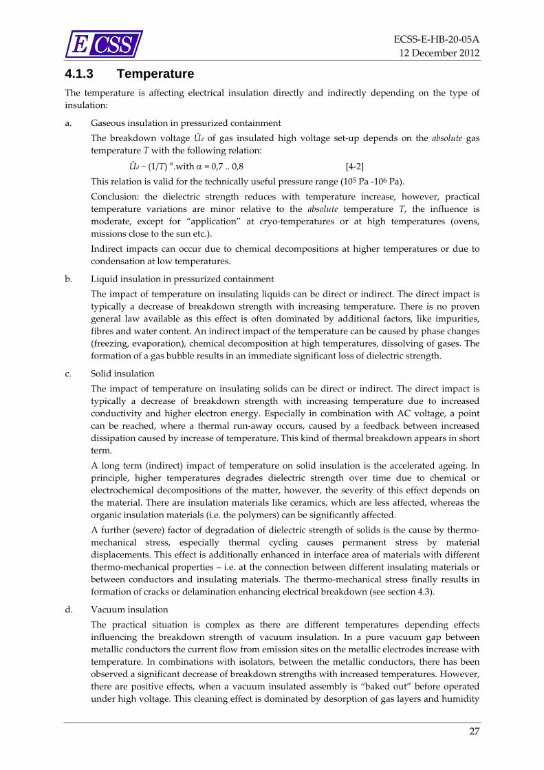
field, moving and forming bridges and strings between conductors as illustrated in Figure 4‐1.
ECSS‐E‐HB‐20‐05A
12 December 2012
29
Figure 4‐1: Arc Caused by Particle Bridge
4.1.6 Plasma
Spacecrafts are exposed to various plasma environments as described and defined in
ECSS‐E‐ST‐10‐04C. For high voltage designs there are principally two effects to be considered:
Because of their higher mobility, electrons preferentially accumulate on exposed spacecraft
surfaces, causing them to charge negatively. In plasmas, charging can reach hundreds or
thousands of volts.
For high potential (high voltage) surfaces, in dense plasmas, ions and electrons are drawn to
negative and positive regions respectively, allowing a current to flow through the plasma. This
acts as a current drain on high voltage systems. Even subsystems with relatively “low” high
voltages, as such as solar generators can be affected.
Further details on spacecraft‐plasma interactions can be found in the ECSS‐E‐ST‐20‐06C (Spacecraft
Charging) standard.
As a consequence, plasmas can result in a leakage current or an immediate breakdown with
uncovered high voltage conductors. Furthermore, in combination with high voltages, surfaces of
insulating materials (exposed to plasma) can charge up and increase the electrical field stress on
insulations.
4.1.7 Mechanical
For completeness, although not specific for high voltage design, but typical for any equipment on
spacecraft, there are typical mechanical environmental conditions:
Vibration loads
Shock loads
These loads are caused mainly by the launcher (vibration) or by satellite deployment mechanisms
(shock). More details can be found in ECSS‐E‐ST‐32C (Structural general requirements).
As a possible consequence: solid electrical insulations and enclosures can crack, liquid can form gas
bubbles under certain conditions, and contained gaseous insulations can be subject to leaks.
High voltage electrode Ground electrode
ECSS‐E‐HB‐20‐05A
12 December 2012
30
4.2 Electrical insulation
4.2.1 Categories of insulation Electrical insulation is a mandatory key technology in “terrestrial” power applications, as high voltage
power generation and transmission as well as in electronic applications. From these applications the
electrical insulation has been categorized into:
Gaseous insulation
Liquid insulation
Solid insulation
Vacuum insulation
In addition, there are in use “mixes” across these categories, like composites of gaseous‐solid,
gaseous‐liquid, and solid‐vacuum.
For space applications, the classical categorization is fully valid with some specific considerations as
discussed in more detail in the following sections. Since the electrical breakdown is the life limiting
factor for all classes of insulation, the basic breakdown mechanisms are discussed for each category.
4.2.2 Gaseous insulation The most common gaseous insulation on earth is air as it is the natural environment for any
equipment on ground – as long as it is not fully encapsulated and exposed to a different environment
(other gases, liquid, solid, vacuum). In general the properties of gaseous insulation can be classified as
follows:
Insulation strengths: low compared to liquid, solid or vacuum insulation
Low degradation over lifetime
Low sensitivity to temperature and humidity
Breakdown strength is precisely predictable and repeatable under consideration of parameters
for geometry, distance, temperature and humidity
Radiation can lead to pre‐ionization, which typically does not lower the breakdown strength,
but narrows the scattering of breakdown voltage values.
Typical properties for various gases are given in the Table 4‐2. Note that these properties are defined
for normal ambient pressure and temperature.
For impact of
temperature ‐ see section 4.1.3 (equation [4‐2]):
breakdown strengths reduces slightly with temperature.
pressure variation close to ambient and higher ‐ see 4.1.2 (equation [4‐1]):
breakdown strength increases with higher pressure.
low pressure range – see section 4.3.4 (Paschen curve):
there is always very low minimum breakdown strength at low pressure, the “Paschen
Minimum”.
ECSS‐E‐HB‐20‐05A
12 December 2012
31
geometry:
Electrical breakdown field strength increases slightly with decreasing gap distance. This effect is
moderate for the distance range below 1 mm; above 1 mm distance it is less significant.
Geometries with non‐homogeneous electrical field (see section 5.1.3) typically have higher
breakdown limits; however, they show partial discharges (corona) at lower voltages –
compared to geometries with homogeneous field distribution.
With the objective to achieve a good electrical insulation for technical applications, typically ambient
air or nitrogen (N2) is used in encapsulated pressurized vessels. Higher insulation strength can be
achieved by using Sulfurhexafluoride (SF6). More information on practical insulation design is given
in section 5.2.2.
Other gases like CO2, H2 or as the inert gases (He, Ne, Ar, Kr, Xe) can be used due to other technical
reasons or because they are naturally present.
In view of space exploration missions to other planets, it should be highlighted that the specific local
atmosphere are composed of:
Venus, Mars: primarily carbon dioxide
Jupiter, Saturn, Uranus, Neptune: hydrogen‐helium atmospheres
Titan (moon of Saturn) and Triton (moon of Neptune): mainly nitrogen
Other bodies within the Solar System with extremely thin atmospheres not in equilibrium:
Moon (sodium gas), Mercury (sodium gas), Europa (oxygen), Io (sulphur), Escalades (water
vapour).
Of course the specific different pressure levels have impact as well. For further details see section 4.1
(impact of environment), section 4.3.2 (for breakdown mechanisms) and section 5.2.4 (for practical
insulation design).
ECSS‐E‐HB‐20‐05A
12 December 2012
32
Table 4‐2: Properties of gaseous insulations
(see Notes 1, 2)
Gas Density Thermal
conductivity
Evaporation
temperature
Electrical
breakdown
field strength (see Note 3)
g/dm3 W/m K °C kV/mm
Air 1,21 25,6∙10‐3 ‐ 3,2
N2 1,17 25,5∙10‐3 ‐195,8 3,3
O2 1,33 26∙10‐3 ‐183,0 2,9
CO2 1,84 16∙10‐3 ‐78,5 2,9
H2 0,08 179∙10‐3 ‐252,8 1,9
He 0,17 149∙10‐3 ‐269,0 1,0
Ne 0,84 48,3∙10‐3 ‐246,0 0,29
Ar 1,66 17,5∙10‐3 ‐185,9 0,65
Kr 3,48 9,4∙10‐3 ‐152,9 0...8
Xe 5,50 5,5∙10‐3 ‐170,1 ‐
SF6 6,15 18,8∙10‐3 ‐63,8 8,9
Note 1: Important: all values for the properties in this table are for general information only. For
use in specific applications refer to individual data sheets and/or dedicated test data.
Note 2: all properties referred to a temperature of 20 °C / pressure 1 atm = 1013 mbar = 1013 hPa
Note 3: electrical breakdown field strengths for a homogeneous field with a gap distance of 1 cm
under short‐term stress
The electrical breakdown mechanism is explained in section 4.3.2. In principle the breakdown
strengths of gases is independent of long‐term effects – there is no ageing and degradation, except if
the gas composition changes over time.
For uniform electrical fields (plane‐to‐plane configuration) the electrical breakdown voltage can be
easily deducted from the electrical breakdown field strengths by the equation [4‐1].
For insulating gaps with unsymmetrical, strong non‐uniform electrical fields there exists a significant
polarity effect. For geometries with the same gap distances the following behaviour can be considered:
Uniform electrical fields lead to the highest breakdown voltages
Non uniform electrical fields lead to a lower breakdown voltage compared to uniform fields
Positive voltages applied to the electrode with the higher electrical field strength, in non‐
uniform fields, leads to a lower breakdown voltage than negative voltages applied to the
electrode with the higher electrical field strengths
Pre‐discharges (corona) appear at the negative electrode in non‐uniform fields if the electrical
breakdown field strength (i.e. as given Table 4‐2) is exceeded, the corona can stay stable until
the voltage is raised to the level of breakdown voltage of the specific configuration.
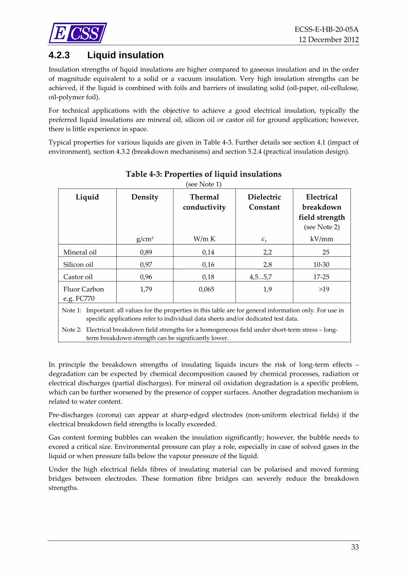
ECSS‐E‐HB‐20‐05A
12 December 2012
33
4.2.3 Liquid insulation Insulation strengths of liquid insulations are higher compared to gaseous insulation and in the order
of magnitude equivalent to a solid or a vacuum insulation. Very high insulation strengths can be
achieved, if the liquid is combined with foils and barriers of insulating solid (oil‐paper, oil‐cellulose,
oil‐polymer foil).
For technical applications with the objective to achieve a good electrical insulation, typically the
preferred liquid insulations are mineral oil, silicon oil or castor oil for ground application; however,
there is little experience in space.
Typical properties for various liquids are given in Table 4‐3. Further details see section 4.1 (impact of
environment), section 4.3.2 (breakdown mechanisms) and section 5.2.4 (practical insulation design).
Table 4‐3: Properties of liquid insulations (see Note 1)
Liquid Density Thermal
conductivity
Dielectric
Constant
Electrical
breakdown
field strength (see Note 2)
g/cm3 W/m K r kV/mm
Mineral oil 0,89 0,14 2,2 25
Silicon oil 0,97 0,16 2,8 10‐30
Castor oil 0,96 0,18 4,5...5,7 17‐25
Fluor Carbon
e.g. FC770
1,79 0,065 1,9 >19
Note 1: Important: all values for the properties in this table are for general information only. For use in
specific applications refer to individual data sheets and/or dedicated test data.
Note 2: Electrical breakdown field strengths for a homogeneous field under short‐term stress – long‐
term breakdown strength can be significantly lower.
In principle the breakdown strengths of insulating liquids incurs the risk of long‐term effects –
degradation can be expected by chemical decomposition caused by chemical processes, radiation or
electrical discharges (partial discharges). For mineral oil oxidation degradation is a specific problem,
which can be further worsened by the presence of copper surfaces. Another degradation mechanism is
related to water content.
Pre‐discharges (corona) can appear at sharp‐edged electrodes (non‐uniform electrical fields) if the
electrical breakdown field strengths is locally exceeded.
Gas content forming bubbles can weaken the insulation significantly; however, the bubble needs to
exceed a critical size. Environmental pressure can play a role, especially in case of solved gases in the
liquid or when pressure falls below the vapour pressure of the liquid.
Under the high electrical fields fibres of insulating material can be polarised and moved forming
bridges between electrodes. These formation fibre bridges can severely reduce the breakdown
strengths.
ECSS‐E‐HB‐20‐05A
12 December 2012
34
4.2.4 Solid insulation Solid insulation is provided by broad choices of different materials, broadly classified into:
Inorganic materials: ceramic, glass
Organic materials: polymers, natural materials (cellulose, paper, micanite).
With the broad variety of available solid insulation materials, there is consequently a wide spectrum
of material properties. Very generally for solid insulation materials it can be stated:
Insulation strengths exhibits a wide range depending on the material is typically higher than for
gaseous insulations, and for the “good” a solid insulator comparable to liquid insulation.
Degradation over lifetime is expected and can be significantly enhanced, if partial discharges
are present.
Breakdown strength has a wide scatter and depending on geometry, manufacturing process,
environmental parameters and pre‐stress.
Short‐term strength (seconds, minutes) is typically much higher than long term strengths
(hours, days).
Sensitive to temperature, especially thermo‐mechanical stress and humidity (for organic
materials). High temperature accelerates ageing and typically increases the conductivity of the
insulation.
Some materials (e.g. some polymers) degrade with radiation, however, the majority of materials
are very stable (w.r.t. typical space radiation environments).
Pressure does not affect the internal electrical strengths of the solid materials, however, if gas
filled gaps or void are present, pressure‐related effects should be considered.
Geometries featuring sharp‐edged embedded electrodes and conductors embark the risk of
partial discharges and thus significant reduction of lifetime.
Sensitive to internal contamination: particle pollution can lead to increase the electrical field and
so trig a local accelerated degradation of the material due to manufacturing process
Typical properties for various solid materials are presented in Table 4‐4, Table 4‐5 and Table 4‐6.
Further details see section 4.1 (impact of environment), section 4.3.2 (breakdown mechanisms) and
section 5.2.4 (practical insulation design).
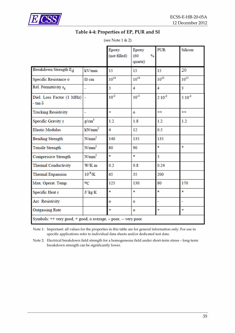
ECSS‐E‐HB‐20‐05A
12 December 2012
35
Table 4‐4: Properties of EP, PUR and SI
(see Note 1 & 2)
Note 1: Important: all values for the properties in this table are for general information only. For use in
specific applications refer to individual data sheets and/or dedicated test data.
Note 2: Electrical breakdown field strength for a homogeneous field under short‐term stress – long‐term
breakdown strength can be significantly lower.
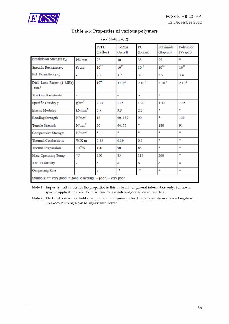
ECSS‐E‐HB‐20‐05A
12 December 2012
36
Table 4‐5: Properties of various polymers
(see Note 1 & 2)
Note 1: Important: all values for the properties in this table are for general information only. For use in
specific applications refer to individual data sheets and/or dedicated test data.
Note 2: Electrical breakdown field strength for a homogeneous field under short‐term stress – long‐term
breakdown strength can be significantly lower.
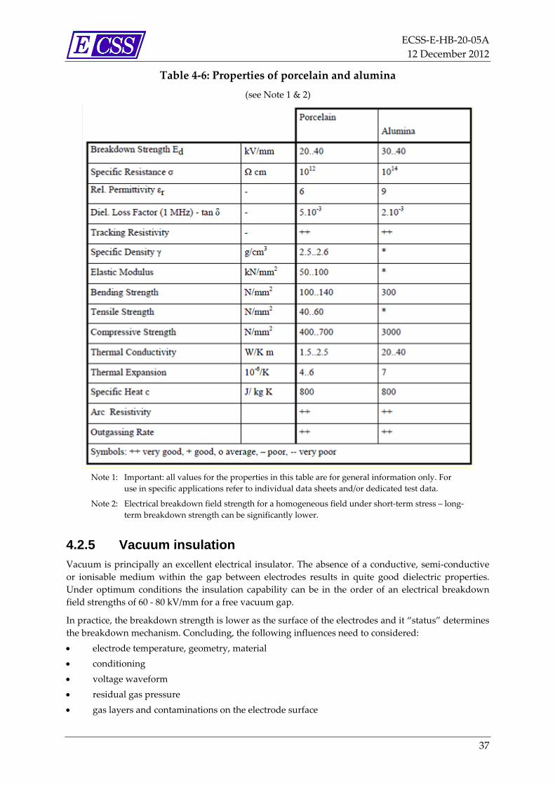
ECSS‐E‐HB‐20‐05A
12 December 2012
37
Table 4‐6: Properties of porcelain and alumina
(see Note 1 & 2)
Note 1: Important: all values for the properties in this table are for general information only. For
use in specific applications refer to individual data sheets and/or dedicated test data.
Note 2: Electrical breakdown field strength for a homogeneous field under short‐term stress – long‐
term breakdown strength can be significantly lower.
4.2.5 Vacuum insulation Vacuum is principally an excellent electrical insulator. The absence of a conductive, semi‐conductive
or ionisable medium within the gap between electrodes results in quite good dielectric properties.
Under optimum conditions the insulation capability can be in the order of an electrical breakdown
field strengths of 60 ‐ 80 kV/mm for a free vacuum gap.
In practice, the breakdown strength is lower as the surface of the electrodes and it “status” determines
the breakdown mechanism. Concluding, the following influences need to considered:
electrode temperature, geometry, material
conditioning
voltage waveform
residual gas pressure
gas layers and contaminations on the electrode surface
ECSS‐E‐HB‐20‐05A
12 December 2012
38
A significant worsening of the breakdown strength can be associated to the presence of solid insulator
in the vacuum gap, as it is typically the case, when spacers and feedthroughs are needed. Depending
on the solid material, the shape of the insulator and the conditioning, the electrical breakdown field
strength can be reduced by more than an order of magnitude (compared to the “free” gap).
Further details see section 4.1 (impact of environment), section 4.3.2 (breakdown mechanisms) and
section 5.2.5 (practical insulation design).
4.2.6 Composites Composites of insulating materials are used to combine the different properties of materials, typically
to achieve improvements of some physical properties. The “classical” composites of electrical
insulation materials are the following:
liquid‐solid
This combination it typically used to increase the electrical strength w.r.t. a pure liquid system:
the liquid is combined with layers of a foil or an immersed structure. Oil combined with
cellulose (paper) or with sheets of polymers (polyethylene, polycarbonate, polypropylene)
ensures good barriers to avoid fibre bridges. The breakdown strength for short and long‐term
effects increases by a factor of 2 to 5.
solid‐gas
The combination of polymer foils with gas under pressure is used in a few applications to
achieve high breakdown strengths. To be effective, this measure requires significant high
pressure.
solid‐solid
Composites of different solid material are used to improve mechanical, thermal and thermo‐
mechanical properties, typical relevant examples are printed circuit boards (glass fibre
embedded in epoxy resin), inorganic powders (glass, ceramic) as fillers in polymeric resins.
solid‐vacuum
Polymeric foils in combination with vacuum are used for cryogenic high voltage cables (i.e. in
superconductive equipments).
An organic or inorganic powder (boron nitride) in combination with vacuum is proposed as an
approach for high power space applications. (Reference: see results of ESA Contract 18697/04
and European Patent Application EP0993238). The powder is mechanically compressed in a
containment embedding the high voltage assemblies.
4.3 Life limiting factors
4.3.1 Perspective From the perspective of an electrical insulation the end of life is reached with the loss or degradation
of the electrical insulation. This loss of electrical insulation can be seen as the threshold, where
according to the applied voltage a certain current is exceeded. In most of the cases, this loss of
insulation results in a drastic change of state, from high ohmic to a low ohmic state. In practice, the
following are distinguished:
(full) electrical breakdown
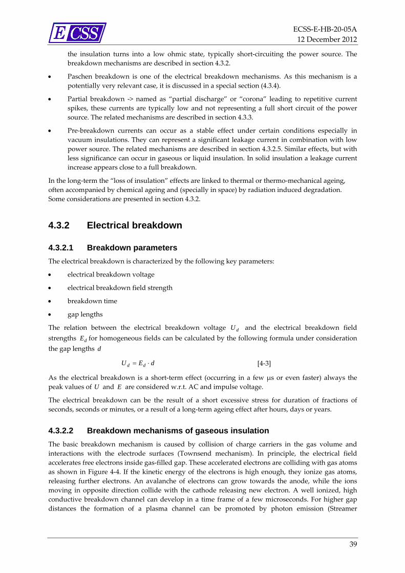
ECSS‐E‐HB‐20‐05A
12 December 2012
39
the insulation turns into a low ohmic state, typically short‐circuiting the power source. The
breakdown mechanisms are described in section 4.3.2.
Paschen breakdown is one of the electrical breakdown mechanisms. As this mechanism is a
potentially very relevant case, it is discussed in a special section (4.3.4).
Partial breakdown ‐> named as “partial discharge” or “corona” leading to repetitive current
spikes, these currents are typically low and not representing a full short circuit of the power
source. The related mechanisms are described in section 4.3.3.
Pre‐breakdown currents can occur as a stable effect under certain conditions especially in
vacuum insulations. They can represent a significant leakage current in combination with low
power source. The related mechanisms are described in section 4.3.2.5. Similar effects, but with
less significance can occur in gaseous or liquid insulation. In solid insulation a leakage current
increase appears close to a full breakdown.
In the long‐term the “loss of insulation” effects are linked to thermal or thermo‐mechanical ageing,
often accompanied by chemical ageing and (specially in space) by radiation induced degradation.
Some considerations are presented in section 4.3.2.
4.3.2 Electrical breakdown
4.3.2.1 Breakdown parameters
The electrical breakdown is characterized by the following key parameters:
electrical breakdown voltage
electrical breakdown field strength
breakdown time
gap lengths
The relation between the electrical breakdown voltage dU and the electrical breakdown field
strengths dE for homogeneous fields can be calculated by the following formula under consideration
the gap lengths d
dEU dd [4‐3]
As the electrical breakdown is a short‐term effect (occurring in a few μs or even faster) always the
peak values of U and E are considered w.r.t. AC and impulse voltage.
The electrical breakdown can be the result of a short excessive stress for duration of fractions of
seconds, seconds or minutes, or a result of a long‐term ageing effect after hours, days or years.
4.3.2.2 Breakdown mechanisms of gaseous insulation
The basic breakdown mechanism is caused by collision of charge carriers in the gas volume and
interactions with the electrode surfaces (Townsend mechanism). In principle, the electrical field
accelerates free electrons inside gas‐filled gap. These accelerated electrons are colliding with gas atoms
as shown in Figure 4‐4. If the kinetic energy of the electrons is high enough, they ionize gas atoms,
releasing further electrons. An avalanche of electrons can grow towards the anode, while the ions
moving in opposite direction collide with the cathode releasing new electron. A well ionized, high
conductive breakdown channel can develop in a time frame of a few microseconds. For higher gap
distances the formation of a plasma channel can be promoted by photon emission (Streamer
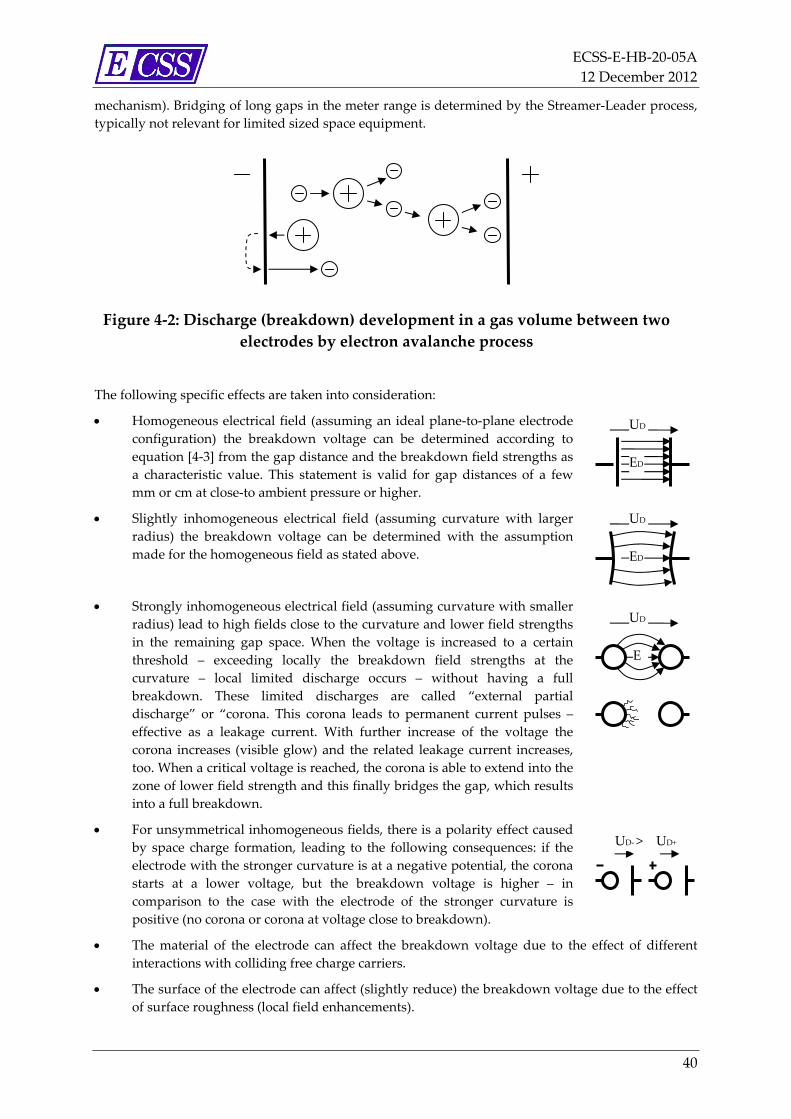
ECSS‐E‐HB‐20‐05A
12 December 2012
40
mechanism). Bridging of long gaps in the meter range is determined by the Streamer‐Leader process,
typically not relevant for limited sized space equipment.
Figure 4‐2: Discharge (breakdown) development in a gas volume between two
electrodes by electron avalanche process
The following specific effects are taken into consideration:
Homogeneous electrical field (assuming an ideal plane‐to‐plane electrode
configuration) the breakdown voltage can be determined according to
equation [4‐3] from the gap distance and the breakdown field strengths as
a characteristic value. This statement is valid for gap distances of a few
mm or cm at close‐to ambient pressure or higher.
Slightly inhomogeneous electrical field (assuming curvature with larger
radius) the breakdown voltage can be determined with the assumption
made for the homogeneous field as stated above.
Strongly inhomogeneous electrical field (assuming curvature with smaller
radius) lead to high fields close to the curvature and lower field strengths
in the remaining gap space. When the voltage is increased to a certain
threshold – exceeding locally the breakdown field strengths at the
curvature – local limited discharge occurs – without having a full
breakdown. These limited discharges are called “external partial
discharge” or “corona. This corona leads to permanent current pulses –
effective as a leakage current. With further increase of the voltage the
corona increases (visible glow) and the related leakage current increases,
too. When a critical voltage is reached, the corona is able to extend into the
zone of lower field strength and this finally bridges the gap, which results
into a full breakdown.
For unsymmetrical inhomogeneous fields, there is a polarity effect caused
by space charge formation, leading to the following consequences: if the
electrode with the stronger curvature is at a negative potential, the corona
starts at a lower voltage, but the breakdown voltage is higher – in
comparison to the case with the electrode of the stronger curvature is
positive (no corona or corona at voltage close to breakdown).
The material of the electrode can affect the breakdown voltage due to the effect of different
interactions with colliding free charge carriers.
The surface of the electrode can affect (slightly reduce) the breakdown voltage due to the effect
of surface roughness (local field enhancements).
ED
UD
UD‐ > UD+
UD
E
ED
UD
ECSS‐E‐HB‐20‐05A
12 December 2012
41
A solid insulator placed between two electrodes can reduce the
breakdown strengths as surface layers (water, contamination) can change
distribution of the electrical field significantly. By increasing the “creepage
path” lengths of an insulator, this effect can be partially or fully
compensated.
Furthermore, the “triple‐junction area” in the corner between two
insulation media and the metal electrode can affect the breakdown
strength (see section 5.1.9).
The gaseous insulation is typically “self‐healing”: after removing and reapplying the power
source the insulation recovers to its initial strengths.
The characteristic of a gaseous insulation breakdown is very well reproducible.
4.3.2.3 Breakdown mechanisms of liquid insulation
There is a common understanding, that very different basic breakdown mechanisms are driving the
electric strengths of liquid insulation depending on the time of exposure to voltage and on
environmental parameters:
A pure collision mechanism in the liquid phase– comparable to the collision breakdown in
gaseous insulation (see Figure 4‐4.)– can only be assumed under extremely high field strengths,
which are in practice never reached, as other effects are dominating the breakdown process
(further explained below). So relevance of this effect is given only in very pure liquids (or
liquefied gases) under short‐term pulse stress (below μs).
A “hidden gas breakdown” is assumed to occur at much lower electrical field strengths than the
collision breakdown in the liquid phase. Gas bubbles can be formed easily by local overheating
due to high field strengths in combination with electron collisions and conductivity. It has been
noticed, that there is a typical dependency of the breakdown strengths in liquids on the
pressure, which is in line with the explanation with the hidden gas breakdown (lower pressure
results in lower strength). This breakdown mechanism is effective in a short‐term regime
between a few μs and seconds. A good degassing of a liquid and a sufficient pressurization is
useful to ensure a high quality of the liquid insulation.
A breakdown related to particles and fibres contributes to a considerable reduction of the
electrical strengths in the time domain of seconds and minutes. It has been clearly confirmed,
that particles present in the liquid are moved under in the force of the electrical field. Especially
particles and fibres of isolating material can charge and react under field force to form fibre
bridges or bouncing with high velocities between electrodes. As the natures of such
contaminations are difficult to control, this effect is a main driver for breakdown in the mid‐
term regime between a few seconds and minutes. A method to reduce this effect is to introduce
barriers in the high electrically stressed volume of a liquid insulation to prevent building up
“fibre bridges” and to restrict particle motion as it is practically done in power industries by
oil/paper, oil/wood, oil/cellulose or oil/polymer‐foil combination. A filtering and cleaning of an
insulating liquid is proposed in additions to ensure a high quality of the liquid insulation.
As a long‐term effect, the degradation of the electrical strengths of a liquid can be related to
chemical processes (oxidation, decomposition) and absorption of other substances. Often
absorption of water / humidity plays an important role. Typical countermeasures are a good
hermetical encapsulation, sometime the use of chemical absorbers / cleaning and a proper
selection of materials embedded in the liquid (for example: avoiding uncovered copper
materials in oil).
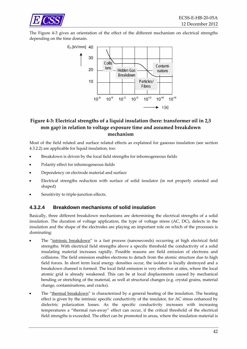
ECSS‐E‐HB‐20‐05A
12 December 2012
42
The Figure 4‐3 gives an orientation of the effect of the different mechanism on electrical strengths
depending on the time domain.
Figure 4‐3: Electrical strengths of a liquid insulation (here: transformer oil in 2,5
mm gap) in relation to voltage exposure time and assumed breakdown
mechanism
Most of the field related and surface related effects as explained for gaseous insulation (see section
4.3.2.2) are applicable for liquid insulation, too:
Breakdown is driven by the local field strengths for inhomogeneous fields
Polarity effect for inhomogeneous fields
Dependency on electrode material and surface
Electrical strengths reduction with surface of solid insulator (in not properly oriented and
shaped)
Sensitivity to triple‐junction effects.
4.3.2.4 Breakdown mechanisms of solid insulation
Basically, three different breakdown mechanisms are determining the electrical strengths of a solid
insulation. The duration of voltage application, the type of voltage stress (AC, DC), defects in the
insulation and the shape of the electrodes are playing an important role on which of the processes is
dominating:
The “intrinsic breakdown” is a fast process (nanoseconds) occurring at high electrical field
strengths. With electrical field strengths above a specific threshold the conductivity of a solid
insulating material increases rapidly. Possible reasons are field emission of electrons and
collisions. The field emission enables electrons to detach from the atomic structure due to high
field forces. In short term local energy densities occur, the isolator is locally destroyed and a
breakdown channel is formed. The local field emission is very effective at sites, where the local
atomic grid is already weakened. This can be at local displacements caused by mechanical
bending or stretching of the material, as well at structural changes (e.g. crystal grains, material
change, contaminations, and cracks).
The “thermal breakdown” is characterized by a general heating of the insulation. The heating
effect is given by the intrinsic specific conductivity of the insulator, for AC stress enhanced by
dielectric polarization losses. As the specific conductivity increases with increasing
temperatures a “thermal run‐away” effect can occur, if the critical threshold of the electrical
field strengths is exceeded. The effect can be promoted in areas, where the insulation material is
10-9 10-6 10-3 10-0 10+3 10+6 10+9
t [s]
40
30
20
10
Ed [kV/mm]
Hidden Gas Breakdown
Particles/ Fibres
Collisions Contami-
nations

ECSS‐E‐HB‐20‐05A
12 December 2012
43
deviating (higher) electric properties – at discontinuities or at more thermally isolated areas in a
volume of material. The heating can take place over seconds, minutes or hours; however, the
run‐away effect itself finally leads to a full breakdown within seconds or even faster.
The “partial discharge breakdown” results in a continuous local erosion of the isolation and
leads to breakdown after many hours or even many years. So it is a definite long‐term
mechanism. The root causes are either irregularities like gas bubbles, delamination, cracks in
the insulator or local zones of high electrical field strengths, i.e. at sharp edged electrodes, metal
particle inclusion. Typical examples of irregularities causing partial discharge breakdown
configuration are shown in section 4.3.3. These partial discharges are repetitive and erode the
material starting from the initial irregularities. The resulting erosion channel can not grow
linearly; in fact it develops typical tree‐like structures. When the erosion “tree” bridges a
significant part of the insulating gap, a sudden full breakdown occurs.
It is emphasised, that the electrical breakdown of solids is typically not reversible. With the full
breakdown the isolator is punctured, often a carbonized (more or less conductive) channel is formed.
The remaining electric strengths are a fraction of the original strengths. If the discharge energy is high
enough, isolation can be cracked and fragmented.
As a consequence of the described breakdown mechanisms the following conclusions can be drawn
for solid insulation:
Any non‐homogeneity or discontinuity within the solid insulation material – either macroscopic
or microscopic – can promote a breakdown.
High temperatures are not favourable.
Materials with lower intrinsic conductivity and a low electric loss factor are advantageous in
terms of thermal breakdown.
Due to the complexity of the breakdown mechanisms, a precise prediction of breakdown
strengths is impossible and measured breakdown strengths can vary from sample to sample
very significant due to non‐controllability of the many microscopic and macroscopic driving
parameters. Due to this the prediction curve can be better found by test and statistical approach.
4.3.2.5 Breakdown mechanisms of vacuum insulation
In a “good” vacuum of below 10‐2 Pa (= 10‐4 mbar) the free‐path lengths of electrons is so high, that
collisions with ions are very rare. Thus a collision based avalanche mechanism can not (primarily)
cause an electrical breakdown. Therefore, the intrinsic electrical strength of vacuum is typically much
higher (greater) compared to solid, liquid and gaseous insulation. However, under certain conditions
charge carriers (electrons, ions) as well a gaseous matter and micro particles can be released from
surfaces of electrodes and insulators. In the vacuum gap between two electrons these released charge
carriers, gases or micro‐particles can easily move and “commute” between surfaces causing pre‐
breakdown and breakdown events.
In the following find a brief overview of these basic mechanisms and their relevance to space power
design. Figure 4‐4 shows the complex relations between several space vacuum related processes
which can finally lead to catastrophic failures of a high voltage system. As a result four types of defect
can occur:
power loss by current flow
solid breakdown (irreversible)
surface flashover
volume breakdown
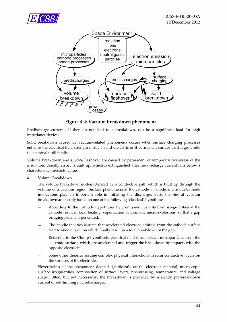
ECSS‐E‐HB‐20‐05A
12 December 2012
44
radiationions
electronsneutral gases
particles
electron emissionmicroparticles
radiationions
electronsneutral gases
particles
radiationions
electronsneutral gases
particlesmicroparticles
cathode processesanode processes
predischargessurfacechargingpredischarges
volumebreakdown
solidbreakdown
surfaceflashover
power losses
Figure 4‐4: Vacuum breakdown phenomena
Predischarge currents, if they do not lead to a breakdown, can be a significant load for high
impedance devices.
Solid breakdown caused by vacuum‐related phenomena occurs when surface charging processes
enhance the electrical field strength inside a solid dielectric or if permanent surface discharges erode
the material until it fails.
Volume breakdown and surface flashover are caused by permanent or temporary overstress of the
insulation. Usually an arc is built up, which is extinguished after the discharge current falls below a
characteristic threshold value.
a. Volume Breakdown
The volume breakdown is characterized by a conductive path which is built up through the
volume of a vacuum region. Surface phenomena at the cathode or anode and anode/cathode
interactions play an important role in initiating the discharge. Basic theories of vacuum
breakdown are mostly based on one of the following ʺclassicalʺ hypotheses:
According to the Cathode hypothesis, field emission currents from irregularities at the
cathode result in local heating, vaporization or dramatic micro‐explosions, so that a gap
bridging plasma is generated.
The anodic theories assume that accelerated electrons emitted from the cathode surface
lead to anodic reaction which finally result in a total breakdown of the gap.
Referring to the Clump hypothesis, electrical field forces detach microparticles from the
electrode surface, which are accelerated and trigger the breakdown by impacts with the
opposite electrode.
Some other theories assume complex physical interactions in semi conductive layers on
the surfaces of the electrodes.
Nevertheless all the phenomena depend significantly on the electrode material, microscopic
surface irregularities, composition of surface layers, pre‐stressing, temperature, and voltage
shape. Often, but not necessarily, the breakdown is preceded by a steady pre‐breakdown
current or self‐limiting microdischarges.
ECSS‐E‐HB‐20‐05A
12 December 2012
45
In space power systems a pure vacuum ʺvolumeʺ breakdown is very rare, because non‐bridged
gaps have a much better voltage hold‐off capability than complex constructions with solid‐
dielectric surfaces, which are vulnerable to ʺslidingʺ discharges. An exception is outgassing
dominated volumes. There the breakdown mechanism can transition from the vacuum
breakdown to the gaseous breakdown, which leads to drastically reduced breakdown voltages.
b. Surface Flashover
The surface flashover occurs as a vacuum discharge along the surface of a solid dielectric, which
is used for construction, i.e. at spacers and feedthroughs, or for encapsulation of components
and systems. Generation and propagation of the discharge are closely involved with surface
phenomena. No single theory is capable of explaining the flashover mechanism, but a selection
of basic hypotheses:
The cathode‐initiated flashover is initiated by electrons emitted from the cathode and
triggering an avalanche process along the insulators surface.
The anode‐initiated flashover assumes surface damage, caused by impacts propagating
with high velocity from the anode to the cathode.
Radiation‐induced flashover can be triggered by ultraviolet illumination at very low
electrical fields, if a critical integrated energy threshold is exceeded.
Some effects influencing the flashover behaviour are the:
Cathode triple junction zones, which are responsible for primary electron emission at
inevitable microscopic irregularities (see section 5.1.9).
Secondary electron emission, which is triggered by energetic particle impact and can
contribute to charge carrier multiplication resulting in local, field enhancing surface
charging.
Gas desorption, which increases drastically, when areas are locally heated by impact or
conductive processes, and can result in a limited gas discharge.
All of these phenomena are extremely sensitive to the material properties, geometry,
composition of surface layers, surface roughness and impurities, pre‐stress, temperature, and
operating conditions of the system.
The flashover voltages of an insulator‐bridged gap are up to one order of magnitude lower than
those of a comparable non‐bridged gap; i.e. stainless‐steel electrode with a homogeneous gap of
10 mm length can withstand AC voltages exceeding 200 kV, an insulator made of PMMA
(polymer: ʺAcrylʺ) breaks down at 35 kV. Typically AC stress results in the lowest hold‐off
capabilities, usually almost two times lower than DC or impulse flashover voltages.
4.3.3 Partial discharges Partial discharges are discharges which do not lead to an immediate breakdown. They can appear in
solid insulations, as well as in liquids and in gas. The typical effect is that a local breakdown occurs in
limited area in a larger volume of insulation. The reasons for this local breakdown can be locally
enhanced high field strengths or a local weakness of the insulation, as well as both reasons in
combination. Typical examples of irregularities causing partial discharges breakdown are shown in
Figure 4‐5.
It is clearly emphasised, that partial discharges in liquid and solid insulation are a significant
accelerating factor for breakdown and for ageing. Therefore the presence of any configuration and
irregularities causing partial discharge should be avoided as far as possible.
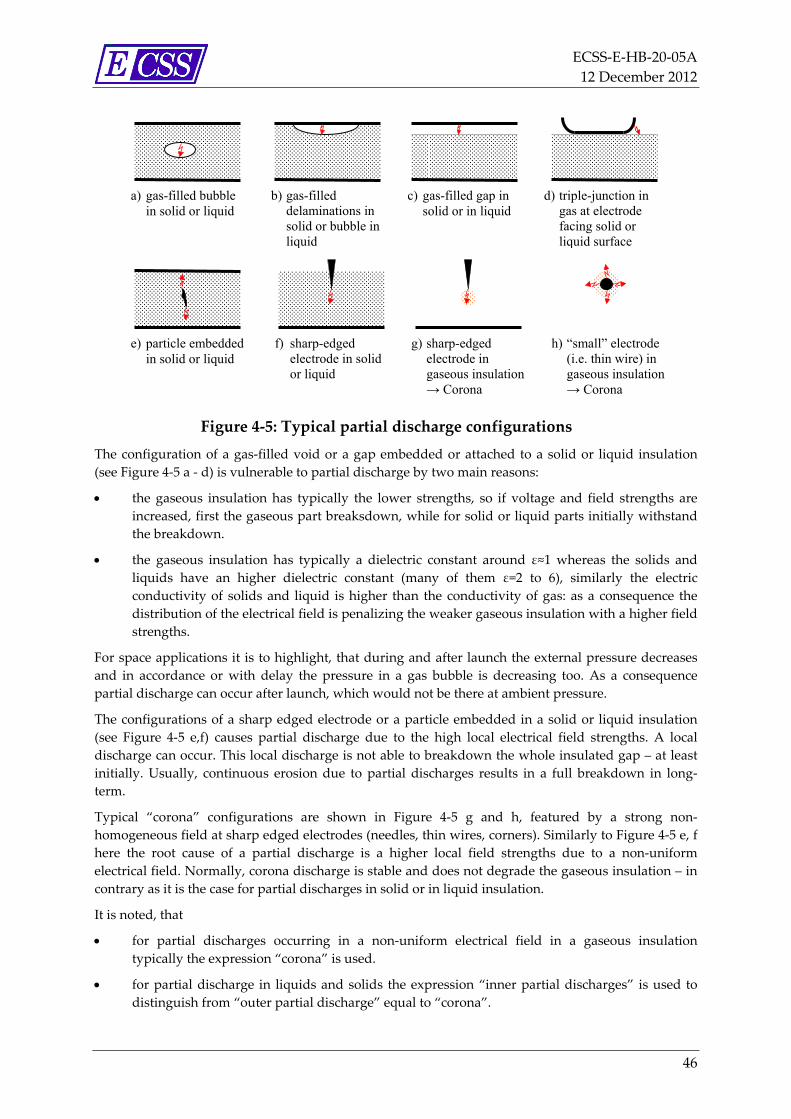
ECSS‐E‐HB‐20‐05A
12 December 2012
46
Figure 4‐5: Typical partial discharge configurations
The configuration of a gas‐filled void or a gap embedded or attached to a solid or liquid insulation
(see Figure 4‐5 a ‐ d) is vulnerable to partial discharge by two main reasons:
the gaseous insulation has typically the lower strengths, so if voltage and field strengths are
increased, first the gaseous part breaksdown, while for solid or liquid parts initially withstand
the breakdown.
the gaseous insulation has typically a dielectric constant around ε≈1 whereas the solids and
liquids have an higher dielectric constant (many of them ε=2 to 6), similarly the electric
conductivity of solids and liquid is higher than the conductivity of gas: as a consequence the
distribution of the electrical field is penalizing the weaker gaseous insulation with a higher field
strengths.
For space applications it is to highlight, that during and after launch the external pressure decreases
and in accordance or with delay the pressure in a gas bubble is decreasing too. As a consequence
partial discharge can occur after launch, which would not be there at ambient pressure.
The configurations of a sharp edged electrode or a particle embedded in a solid or liquid insulation
(see Figure 4‐5 e,f) causes partial discharge due to the high local electrical field strengths. A local
discharge can occur. This local discharge is not able to breakdown the whole insulated gap – at least
initially. Usually, continuous erosion due to partial discharges results in a full breakdown in long‐
term.
Typical “corona” configurations are shown in Figure 4‐5 g and h, featured by a strong non‐
homogeneous field at sharp edged electrodes (needles, thin wires, corners). Similarly to Figure 4‐5 e, f
here the root cause of a partial discharge is a higher local field strengths due to a non‐uniform
electrical field. Normally, corona discharge is stable and does not degrade the gaseous insulation – in
contrary as it is the case for partial discharges in solid or in liquid insulation.
It is noted, that
for partial discharges occurring in a non‐uniform electrical field in a gaseous insulation
typically the expression “corona” is used.
for partial discharge in liquids and solids the expression “inner partial discharges” is used to
distinguish from “outer partial discharge” equal to “corona”.
a) gas-filled bubble in solid or liquid
b) gas-filled delaminations in solid or bubble in liquid
c) gas-filled gap in solid or in liquid
d) triple-junction in gas at electrode facing solid or liquid surface
e) particle embeddedin solid or liquid
f) sharp-edged electrode in solid or liquid
g) sharp-edged electrode in gaseous insulation→ Corona
h) “small” electrode (i.e. thin wire) in gaseous insulation→ Corona
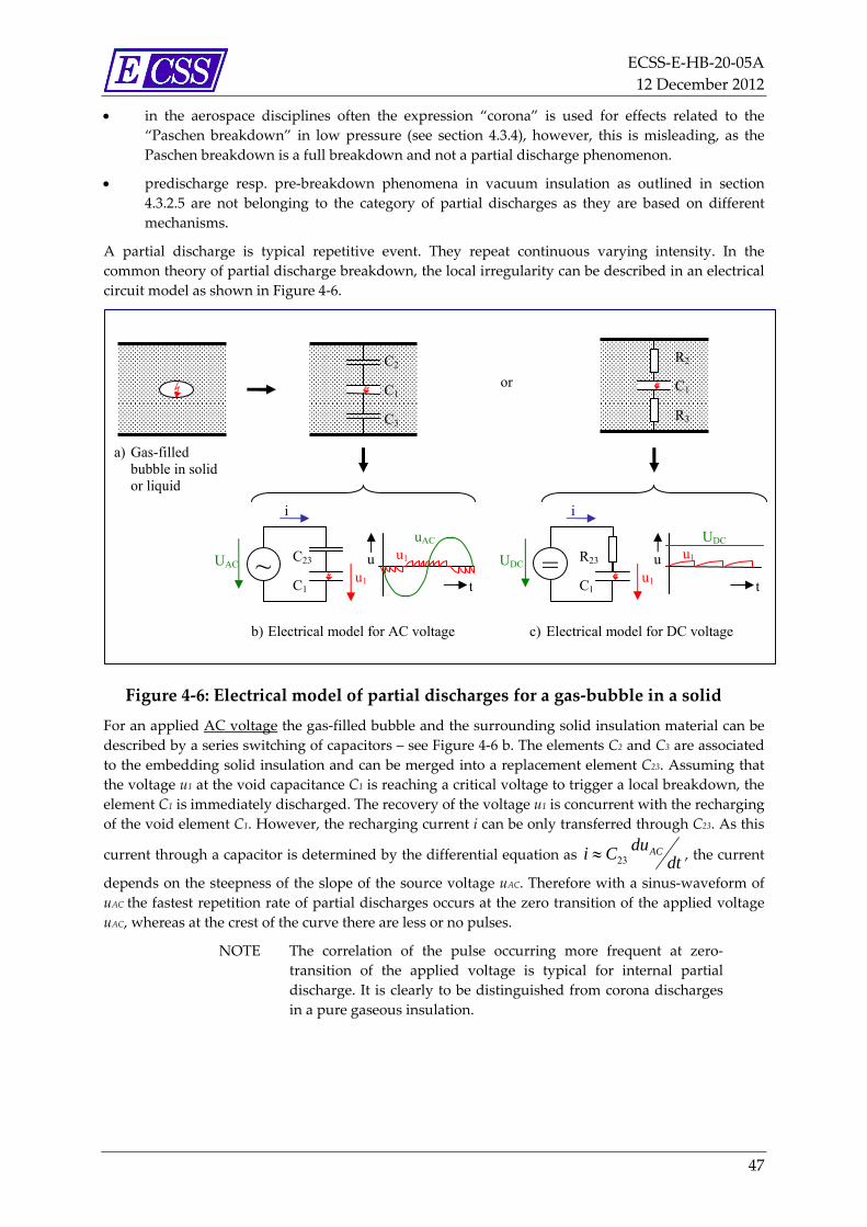
ECSS‐E‐HB‐20‐05A
12 December 2012
47
in the aerospace disciplines often the expression “corona” is used for effects related to the
“Paschen breakdown” in low pressure (see section 4.3.4), however, this is misleading, as the
Paschen breakdown is a full breakdown and not a partial discharge phenomenon.
predischarge resp. pre‐breakdown phenomena in vacuum insulation as outlined in section
4.3.2.5 are not belonging to the category of partial discharges as they are based on different
mechanisms.
A partial discharge is typical repetitive event. They repeat continuous varying intensity. In the
common theory of partial discharge breakdown, the local irregularity can be described in an electrical
circuit model as shown in Figure 4‐6.
Figure 4‐6: Electrical model of partial discharges for a gas‐bubble in a solid
For an applied AC voltage the gas‐filled bubble and the surrounding solid insulation material can be
described by a series switching of capacitors – see Figure 4‐6 b. The elements C2 and C3 are associated
to the embedding solid insulation and can be merged into a replacement element C23. Assuming that
the voltage u1 at the void capacitance C1 is reaching a critical voltage to trigger a local breakdown, the
element C1 is immediately discharged. The recovery of the voltage u1 is concurrent with the recharging
of the void element C1. However, the recharging current i can be only transferred through C23. As this
current through a capacitor is determined by the differential equation as dtduCi AC
23 , the current
depends on the steepness of the slope of the source voltage uAC. Therefore with a sinus‐waveform of
uAC the fastest repetition rate of partial discharges occurs at the zero transition of the applied voltage
uAC, whereas at the crest of the curve there are less or no pulses.
NOTE The correlation of the pulse occurring more frequent at zero‐
transition of the applied voltage is typical for internal partial
discharge. It is clearly to be distinguished from corona discharges
in a pure gaseous insulation.
a) Gas-filled bubble in solid or liquid
b) Electrical model for AC voltage
C1
C2
C3
C1
R2
R3
c) Electrical model for DC voltage
or
u1 ~UAC C23
C1
uAC
u1
t
uu1
=UDCR23
C1
UDC
u1
t
u
i i
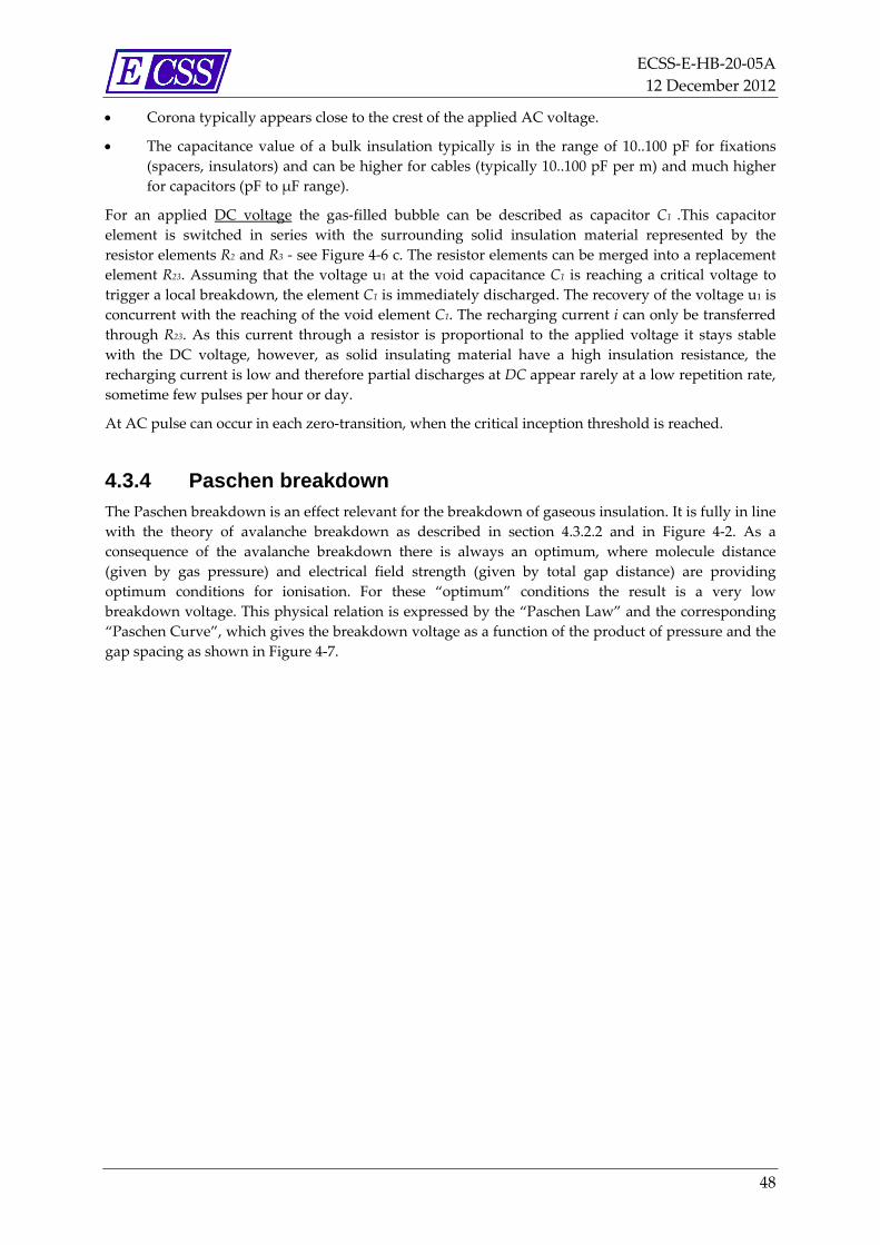
ECSS‐E‐HB‐20‐05A
12 December 2012
48
Corona typically appears close to the crest of the applied AC voltage.
The capacitance value of a bulk insulation typically is in the range of 10..100 pF for fixations
(spacers, insulators) and can be higher for cables (typically 10..100 pF per m) and much higher
for capacitors (pF to μF range).
For an applied DC voltage the gas‐filled bubble can be described as capacitor C1 .This capacitor
element is switched in series with the surrounding solid insulation material represented by the
resistor elements R2 and R3 ‐ see Figure 4‐6 c. The resistor elements can be merged into a replacement
element R23. Assuming that the voltage u1 at the void capacitance C1 is reaching a critical voltage to
trigger a local breakdown, the element C1 is immediately discharged. The recovery of the voltage u1 is
concurrent with the reaching of the void element C1. The recharging current i can only be transferred
through R23. As this current through a resistor is proportional to the applied voltage it stays stable
with the DC voltage, however, as solid insulating material have a high insulation resistance, the
recharging current is low and therefore partial discharges at DC appear rarely at a low repetition rate,
sometime few pulses per hour or day.
At AC pulse can occur in each zero‐transition, when the critical inception threshold is reached.
4.3.4 Paschen breakdown
The Paschen breakdown is an effect relevant for the breakdown of gaseous insulation. It is fully in line
with the theory of avalanche breakdown as described in section 4.3.2.2 and in Figure 4‐2. As a
consequence of the avalanche breakdown there is always an optimum, where molecule distance
(given by gas pressure) and electrical field strength (given by total gap distance) are providing
optimum conditions for ionisation. For these “optimum” conditions the result is a very low
breakdown voltage. This physical relation is expressed by the “Paschen Law” and the corresponding
“Paschen Curve”, which gives the breakdown voltage as a function of the product of pressure and the
gap spacing as shown in Figure 4‐7.
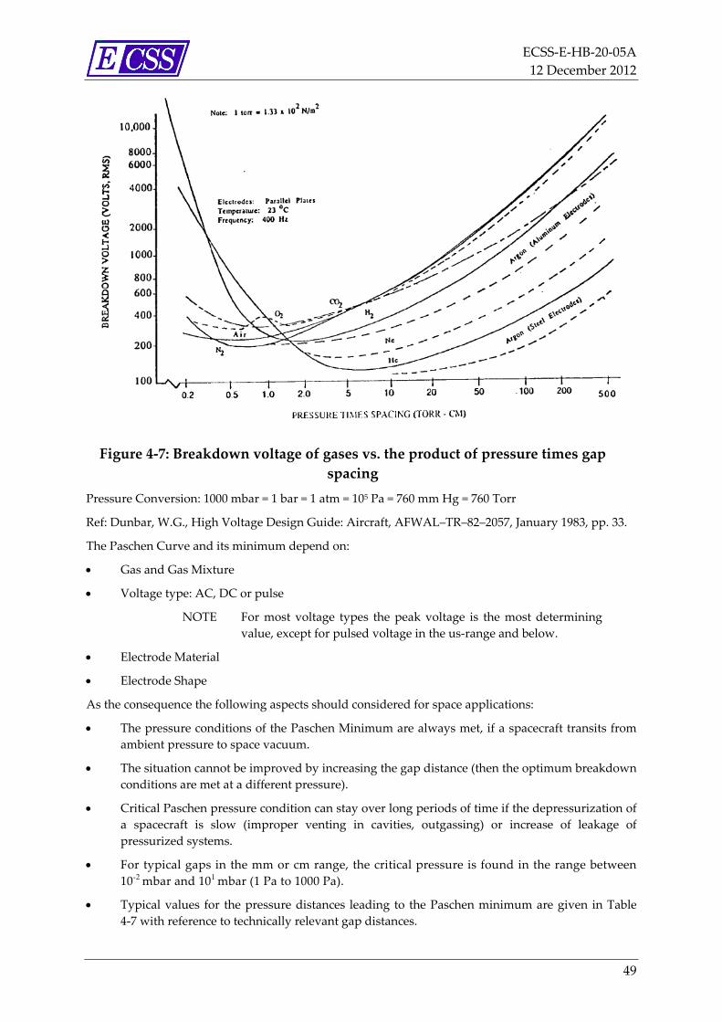
ECSS‐E‐HB‐20‐05A
12 December 2012
49
Figure 4‐7: Breakdown voltage of gases vs. the product of pressure times gap
spacing
Pressure Conversion: 1000 mbar = 1 bar = 1 atm = 105 Pa = 760 mm Hg = 760 Torr
Ref: Dunbar, W.G., High Voltage Design Guide: Aircraft, AFWAL–TR–82–2057, January 1983, pp. 33.
The Paschen Curve and its minimum depend on:
Gas and Gas Mixture
Voltage type: AC, DC or pulse
NOTE For most voltage types the peak voltage is the most determining
value, except for pulsed voltage in the us‐range and below.
Electrode Material
Electrode Shape
As the consequence the following aspects should considered for space applications:
The pressure conditions of the Paschen Minimum are always met, if a spacecraft transits from
ambient pressure to space vacuum.
The situation cannot be improved by increasing the gap distance (then the optimum breakdown
conditions are met at a different pressure).
Critical Paschen pressure condition can stay over long periods of time if the depressurization of
a spacecraft is slow (improper venting in cavities, outgassing) or increase of leakage of
pressurized systems.
For typical gaps in the mm or cm range, the critical pressure is found in the range between
10-2 mbar and 101 mbar (1 Pa to 1000 Pa).
Typical values for the pressure distances leading to the Paschen minimum are given in Table
4‐7 with reference to technically relevant gap distances.
ECSS‐E‐HB‐20‐05A
12 December 2012
50
Special conditions can apply for planetary probes entering atmospheres of other planets and
bodies: the conditions for the relevant atmospheric gas mixtures are evaluated individually.
Table 4‐7: Paschen Minimum for various gases
Breakdown
Voltage
Paschen Minimum
Pressure times
Spacing Pressure for Minimum vs. Gap Spacing
Ud‐min (pd)min (pd)min @ 1 mm @ 1 cm @ 10 cm @ 1 m
Gas V hPa μm hPa mm hPa hPa hPa hPa
SF6 507 3,5 0,0035 3,5 0,35 3,5 10‐02 3,5 10‐03
O2 450 9,3 0,0093 9,3 0,93 9,3 10‐02 9,3 10‐03
CO2 420 6,8 0,0068 6,8 0,68 6,8 10‐02 6,8 10‐03
Air 330 7,3 0,0073 7,3 0,73 7,3 10‐02 7,3 10‐03
N2 240 8,6 0,0086 8,6 0,861 8,6 10‐02 8,6 10‐03
H2 230 14 0,014 14 1,4 0,14 1,4 10‐02
Ne 130 53,2 0,0532 53 5,3 0,53 5,3 10‐02
Ar 94
He 155 53,2 0,0532 53 5,3 0,53 5,3 10‐02
Pressure Conversion: 1000 mbar = 1 bar = 1 atm = 105 Pa = 103 hPa = 760 mm Hg = 760 Torr
Operation of high voltage close to Paschen breakdown conditions should be typically avoided.
Suitable measures are proposed in section 5.1, 5.2.2 and 5.2.5.
4.3.5 Ageing
4.3.5.1 Ageing of gaseous, liquid and vacuum insulation
Gaseous and vacuum insulation are not subject to ageing effects. However, there are some “indirect
effects” to be considered. Liquid insulation is vulnerable to ageing. The specific aspects of the different
insulation types are briefly explained in the following:
For gaseous insulation:
The pressure conditions can change over time, i.e. leakage of a pressurized containment can
result over time into a decay to a critical low pressure.
The chemical composition can change over time, by leakage of tanks etc. or by electrochemical
processes.
As an example: SF6 gas can be subject of decomposition in the presence of humidity and corona.
Nevertheless an effect on gas volume breakdown strength is unlikely, unless a very significant
amount of the gas volume has been changed. However, an indirect effect can occur as the
chemical decomposition can create corrosive by‐products (e.g. SF6 reactions with humid air can
result in aggressive by‐products affecting surfaces of solid insulators).
For liquid insulation:
The chemical composition can change over time, responsible processes can be:
Oxidation (example: mineral oil, acceleration of oxidation in presence of copper)
Partial discharge (destructing molecules or causing polymerisation)
ECSS‐E‐HB‐20‐05A
12 December 2012
51
Radiation (destructing molecules, however, only relevant for extreme high radiation doses).
Increase of water content (especially, if exposed to natural atmosphere)
For encapsulated systems in space environment: the pressure conditions can change over time,
i.e. leakage of a pressurized containment can result over time into decay to lower pressure. If
the vapour pressure of the liquid or of solved gases (contaminants) is reached, gas bubble can
be formed and trigger a breakdown.
As liquid insulations are rarely used in space application, the above mentioned ageing effects
are not further explained here. In case of use of such insulation, it is proposed to make
advantage of available information from power industries and related research.
For vacuum insulation:
The pressure conditions can change over time, i.e. leakage of a pressurized tank nearby can
result over time into a raise to critical high pressure.
Similarly, outgassing from surfaces can cause problems related to local “micro‐atmosphere” –
however, in most cases the outgassing effect decays with long exposure in a vacuum, which
leads typically to an improvement of electrical strengths, not a worsening.
4.3.5.2 Ageing of solid insulation
4.3.5.2.1 Ageing mechanisms
Solid insulations are widely used in space applications and they are subject to various relevant ageing
effects. As the various effects resulting to a breakdown in long‐term are complex and interacting in a
complex matter, there is actually no “universal” approach to explain ageing of solids and to predict
lifetime precisely. The most relevant aspects are explained in the following:
First of all, the final breakdown mechanism is assumed to be electrical and can happen (finally)
in a short‐term. The (final) breakdown mechanism is most likely one of the following: the pure
“intrinsic” electric breakdown, thermal breakdown or partial discharge breakdown as already
addressed in section 4.3.2.4. However, on the way to the breakdown on a long time‐scale of
hours, days or years, there is a significant influence of degradation by mechanical, thermal,
thermo‐mechanical, chemical, electro‐chemical, radiation‐induced, electrically induced
processes as well as by the already addressed partial discharge driven mechanism.
Partial discharges form erosive channels in the insulation. The starting point of the partial
discharge is a weakness in the insulation, often, but not always in an area with higher field
strengths. The erosion channel propagates over time. The channel path is not necessarily
leading straight in the direction of the highest macroscopic electrical field and can subdivide
into many branches forming tree‐like structures (see Figure 4‐8). The electrical breakdown
occurs, when the insulation is weakened by the growing tree – i.e. when branches have been
protruded that a significant part of the insulating gap is bridged. Treeing is often observed in
polymeric insulation.
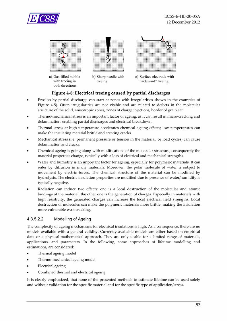
ECSS‐E‐HB‐20‐05A
12 December 2012
52
Figure 4‐8: Electrical treeing caused by partial discharges
Erosion by partial discharge can start at zones with irregularities shown in the examples of
Figure 4‐5). Often irregularities are not visible and are related to defects in the molecular
structure of the solid, anisotropic zones, zones of charge injections, border of grain etc.
Thermo‐mechanical stress is an important factor of ageing, as it can result in micro‐cracking and
delamination, enabling partial discharges and electrical breakdown.
Thermal stress at high temperature accelerates chemical ageing effects; low temperatures can
make the insulating material brittle and creating cracks.
Mechanical stress (i.e. permanent pressure or tension in the material, or load cycles) can cause
delamination and cracks.
Chemical ageing is going along with modifications of the molecular structure, consequently the
material properties change, typically with a loss of electrical and mechanical strengths.
Water and humidity is an important factor for ageing, especially for polymeric materials. It can
enter by diffusion in many materials. Moreover, the polar molecule of water is subject to
movement by electric forces. The chemical structure of the material can be modified by
hydrolysis. The electric insulation properties are modified due to presence of water/humidity is
typically negative.
Radiation can induce two effects: one is a local destruction of the molecular and atomic
bindings of the material, the other one is the generation of charges. Especially in materials with
high resistivity, the generated charges can increase the local electrical field strengths. Local
destruction of molecules can make the polymeric materials more brittle, making the insulation
more vulnerable w.r.t cracking.
4.3.5.2.2 Modelling of Ageing
The complexity of ageing mechanisms for electrical insulations is high. As a consequence, there are no
models available with a general validity. Currently available models are either based on empirical
data or a physical‐mathematical approach. They are only usable for a limited range of materials,
applications, and parameters. In the following, some approaches of lifetime modelling and
estimations, are considered:
Thermal ageing model
Thermo‐mechanical ageing model
Electrical ageing
Combined thermal and electrical ageing
It is clearly emphasized, that none of the presented methods to estimate lifetime can be used solely
and without validation for the specific material and for the specific type of application/stress.
a) Gas-filled bubble with treeing in both directions
b) Sharp needle with treeing
c) Surface electrode with “sideward” treeing

ECSS‐E‐HB‐20‐05A
12 December 2012
53
4.3.5.2.3 Thermal ageing model by Arrhenius
An ageing model based on temperature effects (only) is referring to the “classical” Arrhenius
equation:
kT
WAt aexp
[4‐4]
where:
t lifetime
A adjustable constant
Wa activation energy
k Boltzmann Constant
T temperature
Note: that this equation considers temperature as the only ageing parameter. Electrical ageing
mechanisms are not covered. The adjustable constant A can be determined experimentally. A very
detailed statistical approach is described in the standard IEC 60216‐1.
References are made to:
T.W. Dakin, “Electrical Insulation Deterioration Treated as Chemical Rate Phenomenon”, AIEE
Transactions, Vol. 67, pp. 113‐122, 1948.
T.W. Dakin, “Electrical Insulation Deterioration”, Electrotechnology, Vol. 3, pp. 129‐13‐, 1960.
IEC 60216‐1 “Properties of thermal endurance, Part 1: Ageing procedures and evaluation test results”
– International Standard.
4.3.5.2.4 Thermo-mechanical ageing model by Halpin
For solid materials thermo‐mechanical ageing is an important factor, especially under the assumption,
that formation of cracks and delamination is the root cause of a subsequent electrical failure. Based on
experience with failures in complex printed circuit boards, fatigue related failures due to thermal
cycling are resulting in a typical stress‐lifetime plot as a straight line in a semi‐logarithmic plot. An
example is shown in Figure 4‐9.
Figure 4‐9: Example: Fatigue (thermo‐mechanical stress‐related) failures in
assemblies expressed as stress (∆T – temperature cycle amplitude) over number
of thermal cycles
1 10 100 103 104 105 106
400
300
200
100
∆T [K]
Number of thermal cycles
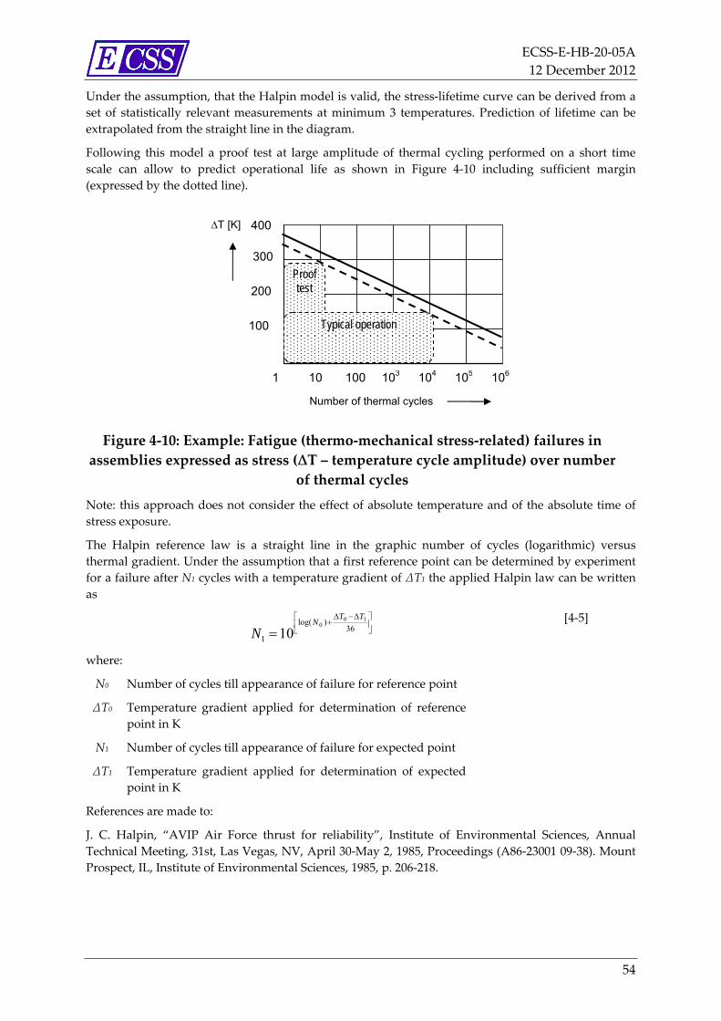
ECSS‐E‐HB‐20‐05A
12 December 2012
54
Under the assumption, that the Halpin model is valid, the stress‐lifetime curve can be derived from a
set of statistically relevant measurements at minimum 3 temperatures. Prediction of lifetime can be
extrapolated from the straight line in the diagram.
Following this model a proof test at large amplitude of thermal cycling performed on a short time
scale can allow to predict operational life as shown in Figure 4‐10 including sufficient margin
(expressed by the dotted line).
Figure 4‐10: Example: Fatigue (thermo‐mechanical stress‐related) failures in
assemblies expressed as stress (∆T – temperature cycle amplitude) over number
of thermal cycles
Note: this approach does not consider the effect of absolute temperature and of the absolute time of
stress exposure.
The Halpin reference law is a straight line in the graphic number of cycles (logarithmic) versus
thermal gradient. Under the assumption that a first reference point can be determined by experiment
for a failure after N1 cycles with a temperature gradient of ΔT1 the applied Halpin law can be written
as
36)log(
1
100
10TT
N
N
[4‐5]
where:
N0 Number of cycles till appearance of failure for reference point
ΔT0 Temperature gradient applied for determination of reference
point in K
N1 Number of cycles till appearance of failure for expected point
ΔT1 Temperature gradient applied for determination of expected
point in K
References are made to:
J. C. Halpin, “AVIP Air Force thrust for reliability”, Institute of Environmental Sciences, Annual
Technical Meeting, 31st, Las Vegas, NV, April 30‐May 2, 1985, Proceedings (A86‐23001 09‐38). Mount
Prospect, IL, Institute of Environmental Sciences, 1985, p. 206‐218.
1 10 100 103 104 105 106
400
300
200
100
∆T [K]
Proof test
Number of thermal cycles
Typical operation
ECSS‐E‐HB‐20‐05A
12 December 2012
55
4.3.5.2.5 Electrical ageing based on inverse power law
The inverse power law considers the electrical field strengths as a driver for the lifetime as expressed
in the following equation:
nECt
[4‐6]
where:
t lifetime,
C adjustable constant
E electrical field strengths
n constant
The constants C and n are investigated experimentally and are only valid for the material, the type of
application and the ageing mechanism, which has been the subject of the experiment. If the ageing
mechanism or relevant parameters change over time, a new curve is determined. Practically, the
lifetime data are collected in a “log E over log t plot” or as “E over log t plot”. The Data points should
indicate a straight line.
4.3.5.2.6 Combined thermal and electrical ageing
A model for combined thermal and electrical ageing was presented by J.P. Crine (see references
below). The mathematical expression determines the lifetime by an exponential factor expressing pure
temperature dependence and a hyperbolic factor representing the influence of the electrical field:
kT
Ee
kT
G
kT
ht
cschexp
20
[4‐7]
where:
t lifetime
h Planck constant
k Boltzmann constant
T temperature
G0 activation energy
e elementary electron charge
λ free path / submicrocavity size
E electrical field strengths
The constants G0 and the parameter λ depend on the material and on the configuration. G0 is
determined by the material’s activation enthalpy and the entropy of free space charges, so it fairly
equivalent to the activation energy as stated in the Arrhenius equation (see eq. [4‐4]). The parameter λ
depends on the electrical field and defines the size of so‐called submicrocavities, assuming the high
electrical field strength is displacing the molecular structure in such a way that the free‐path length of
electrons allows collision based ionization effects. It can be difficult to determine the “unknown”
parameters (G0 and λ) of the equation [4‐7] on a theoretical basis only.
A useful practical approach is to determine the relevant section of the stress‐lifetime curve (E over log t)
experimentally (see Figure 4‐11). In accordance with the model, the resulting graph can be analysed
separating two sections: the left section strongly depends on the electrical field strengths determining the
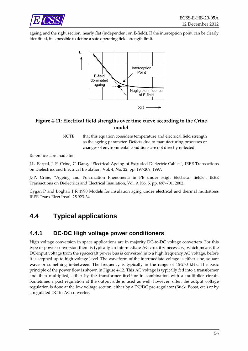
ECSS‐E‐HB‐20‐05A
12 December 2012
56
ageing and the right section, nearly flat (independent on E‐field). If the interception point can be clearly
identified, it is possible to define a safe operating field strength limit.
Figure 4‐11: Electrical field strengths over time curve according to the Crine
model
NOTE that this equation considers temperature and electrical field strength
as the ageing parameter. Defects due to manufacturing processes or
changes of environmental conditions are not directly reflected.
References are made to:
J.L. Parpal, J.‐P. Crine, C. Dang, “Electrical Ageing of Extruded Dielectric Cables”, IEEE Transactions
on Dielectrics and Electrical Insulation, Vol. 4, No. 22, pp. 197‐209, 1997.
J.‐P. Crine, “Ageing and Polarization Phenomena in PE under High Electrical fields”, IEEE
Transactions on Dielectrics and Electrical Insulation, Vol. 9, No. 5, pp. 697‐701, 2002.
Cygan P and Loghari J R 1990 Models for insulation aging under electrical and thermal multistress
IEEE Trans.Elect.Insul. 25 923‐34.
4.4 Typical applications
4.4.1 DC-DC High voltage power conditioners High voltage conversion in space applications are in majority DC‐to‐DC voltage converters. For this
type of power conversion there is typically an intermediate AC circuitry necessary, which means the
DC‐input voltage from the spacecraft power bus is converted into a high frequency AC voltage, before
it is stepped up to high voltage level. The waveform of the intermediate voltage is either sine, square
wave or something in‐between. The frequency is typically in the range of 15‐250 kHz. The basic
principle of the power flow is shown in Figure 4‐12. This AC voltage is typically fed into a transformer
and then multiplied, either by the transformer itself or in combination with a multiplier circuit.
Sometimes a post regulation at the output side is used as well, however, often the output voltage
regulation is done at the low voltage section: either by a DC/DC pre‐regulator (Buck, Boost, etc.) or by
a regulated DC‐to‐AC converter.
E
log t
E-field dominated
ageing
Interception Point
Negligible influence of E-field
ECSS‐E‐HB‐20‐05A
12 December 2012
57
Figure 4‐12: DC/DC power conversion chains for high voltage of an EPC
For the core part of the high voltage generation there are basically two different principles of
conversion into high voltage:
Transformer (with subsequent rectifier/filter for DC) – see Figure 4‐13 a)
Capacitor‐Diode Networks (“Cockroft‐Walton Multiplier”, “Greinacher Cascade”)
as a single cascade: see Figure 4‐13 b) or as a double cascade: see Figure 4‐13 c)
The cascade multiplier is very mass efficient for a low power application (typically of a few Watts
output power); the number of multiplier stages varies between 2 and 20. Higher numbers of stages are
critical with respect to loop stability. Furthermore the ripple of the output voltage and the output
impedance increase significantly.
Voltage step‐up via a transformer is an efficient solution for conversion with power levels above a few
Watts. For high DC output voltages a number of transformer windings can be individually rectified
and switched in series.
It is important to limit the AC stress inside of the high voltage insulation as far as possible; therefore it
is preferred to reduce the AC output voltage per windings in favour of adding the output voltage of a
higher number of rectified smaller high voltage stages. The reduction of AC voltage reduces the risk
of life time limiting partial discharges. Often the voltage per stage is between 600V and 1200V;
however, the selection of the appropriate topology and voltage is typically the outcome of a trade‐off
of many different parameters and aspects.
Spaecraft Power Bus
DC to AC Converter
DC/DC Preregulator
Transformer(s)
DC AC
DC
Cascade - Multiplier
Rectifier / Smoothing
with Postregulator
Low Voltage Section High Voltage Section
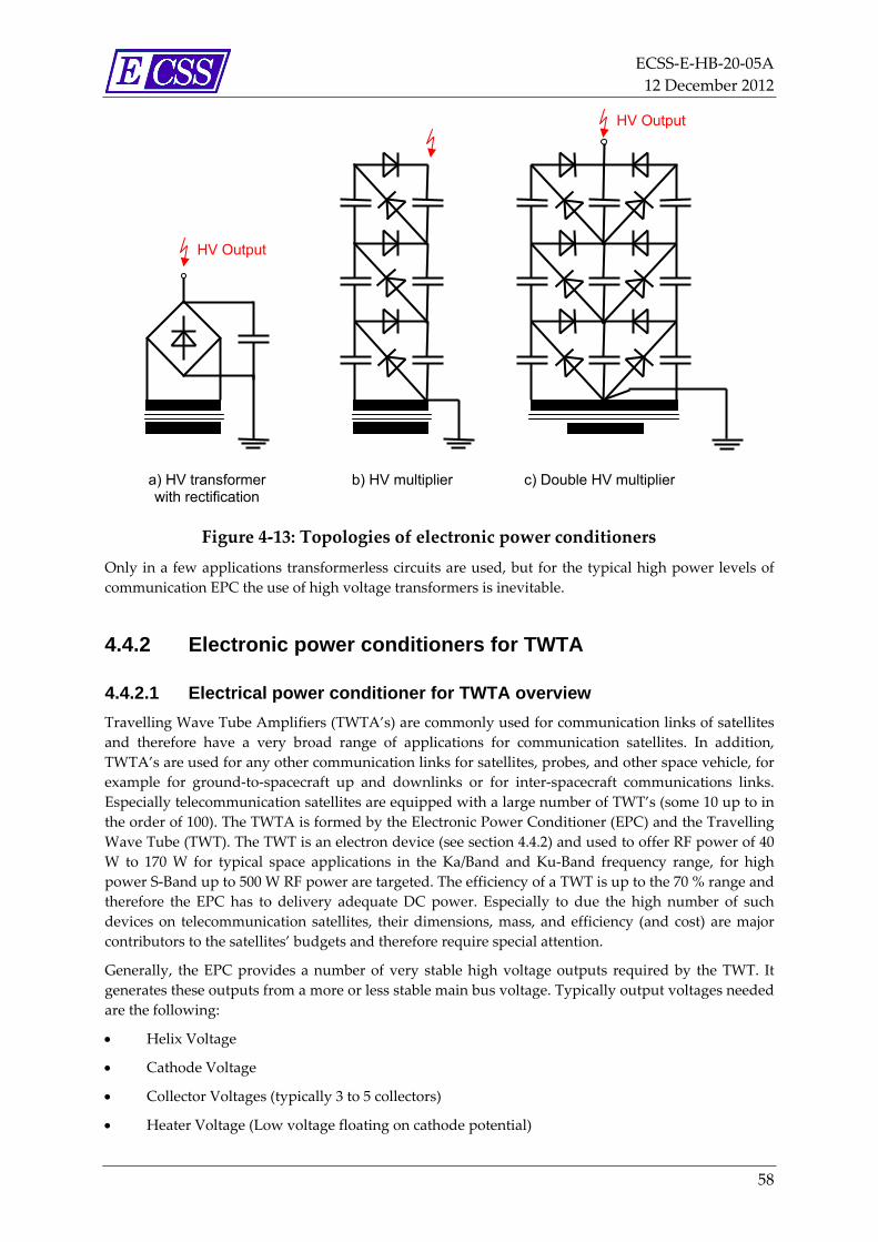
ECSS‐E‐HB‐20‐05A
12 December 2012
58
Figure 4‐13: Topologies of electronic power conditioners
Only in a few applications transformerless circuits are used, but for the typical high power levels of
communication EPC the use of high voltage transformers is inevitable.
4.4.2 Electronic power conditioners for TWTA
4.4.2.1 Electrical power conditioner for TWTA overview
Travelling Wave Tube Amplifiers (TWTA’s) are commonly used for communication links of satellites
and therefore have a very broad range of applications for communication satellites. In addition,
TWTA’s are used for any other communication links for satellites, probes, and other space vehicle, for
example for ground‐to‐spacecraft up and downlinks or for inter‐spacecraft communications links.
Especially telecommunication satellites are equipped with a large number of TWT’s (some 10 up to in
the order of 100). The TWTA is formed by the Electronic Power Conditioner (EPC) and the Travelling
Wave Tube (TWT). The TWT is an electron device (see section 4.4.2) and used to offer RF power of 40
W to 170 W for typical space applications in the Ka/Band and Ku‐Band frequency range, for high
power S‐Band up to 500 W RF power are targeted. The efficiency of a TWT is up to the 70 % range and
therefore the EPC has to delivery adequate DC power. Especially to due the high number of such
devices on telecommunication satellites, their dimensions, mass, and efficiency (and cost) are major
contributors to the satellites’ budgets and therefore require special attention.
Generally, the EPC provides a number of very stable high voltage outputs required by the TWT. It
generates these outputs from a more or less stable main bus voltage. Typically output voltages needed
are the following:
Helix Voltage
Cathode Voltage
Collector Voltages (typically 3 to 5 collectors)
Heater Voltage (Low voltage floating on cathode potential)
b) HV multiplier c) Double HV multiplier
HV Output
HV Output
a) HV transformer with rectification
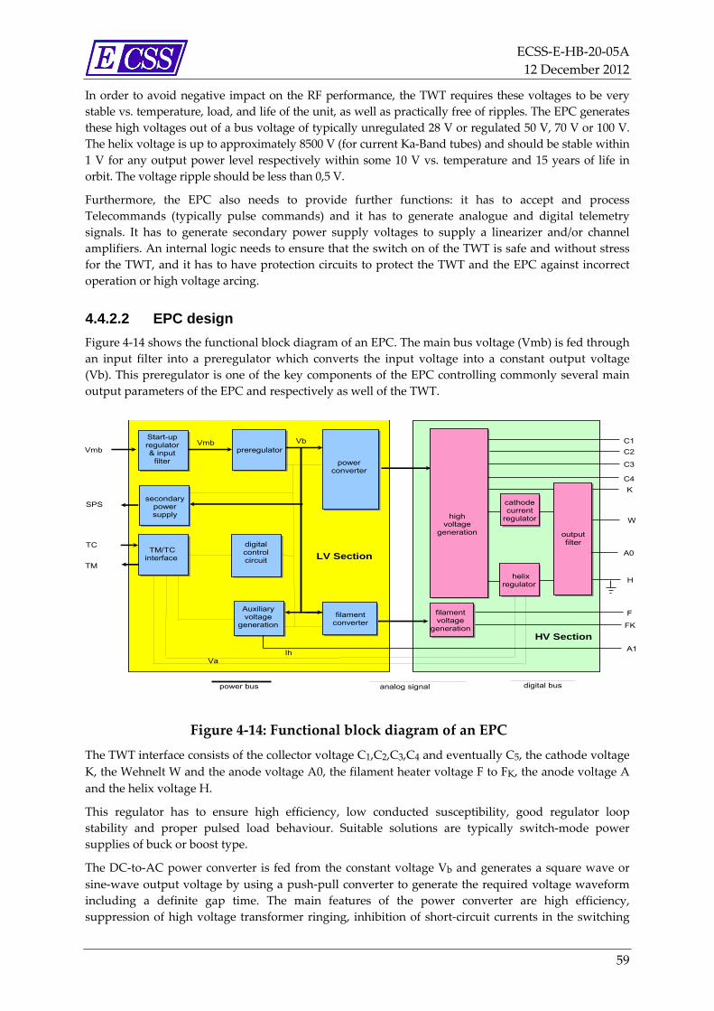
ECSS‐E‐HB‐20‐05A
12 December 2012
59
In order to avoid negative impact on the RF performance, the TWT requires these voltages to be very
stable vs. temperature, load, and life of the unit, as well as practically free of ripples. The EPC generates
these high voltages out of a bus voltage of typically unregulated 28 V or regulated 50 V, 70 V or 100 V.
The helix voltage is up to approximately 8500 V (for current Ka‐Band tubes) and should be stable within
1 V for any output power level respectively within some 10 V vs. temperature and 15 years of life in
orbit. The voltage ripple should be less than 0,5 V.
Furthermore, the EPC also needs to provide further functions: it has to accept and process
Telecommands (typically pulse commands) and it has to generate analogue and digital telemetry
signals. It has to generate secondary power supply voltages to supply a linearizer and/or channel
amplifiers. An internal logic needs to ensure that the switch on of the TWT is safe and without stress
for the TWT, and it has to have protection circuits to protect the TWT and the EPC against incorrect
operation or high voltage arcing.
4.4.2.2 EPC design
Figure 4‐14 shows the functional block diagram of an EPC. The main bus voltage (Vmb) is fed through
an input filter into a preregulator which converts the input voltage into a constant output voltage
(Vb). This preregulator is one of the key components of the EPC controlling commonly several main
output parameters of the EPC and respectively as well of the TWT.
HV Section
power converter
Start-up regulator & input
filter
preregulator Vmb Vmb Vb
Va
power bus analog signal digital bus
LV Section
output filter
cathode current
regulator
helix regulator
high voltage
generation
C1
C2
C3
C4
K
H
A0
FK
Auxiliary voltage
generation
filamentconverter
A1
digital control circuit
Ih
filament voltage
generation
secondary power supply
TC TM/TC
interface
W
SPS
TM
F
Figure 4‐14: Functional block diagram of an EPC
The TWT interface consists of the collector voltage C1,C2,C3,C4 and eventually C5, the cathode voltage
K, the Wehnelt W and the anode voltage A0, the filament heater voltage F to FK, the anode voltage A
and the helix voltage H.
This regulator has to ensure high efficiency, low conducted susceptibility, good regulator loop
stability and proper pulsed load behaviour. Suitable solutions are typically switch‐mode power
supplies of buck or boost type.
The DC‐to‐AC power converter is fed from the constant voltage Vb and generates a square wave or
sine‐wave output voltage by using a push‐pull converter to generate the required voltage waveform
including a definite gap time. The main features of the power converter are high efficiency,
suppression of high voltage transformer ringing, inhibition of short‐circuit currents in the switching

ECSS‐E‐HB‐20‐05A
12 December 2012
60
transistors, and soft recovery for the high voltage diodes. An auxiliary preregulator generates a
second constant output voltage (Vb2) which is used to generate the supply voltages for the internal
electronics. The output of the auxiliary preregulator power is connected to the compensation unit and
to the filament converter. The filament converter is then generating the necessary AC supply voltage
for the TWT filament heating. The filament heater low voltage is floating on the high voltage potential
of the cathode. A soft start is implemented for the filament converter to avoid surge currents when the
tube filament is cold and has then a lower resistance.
An important part of the power chain is the high voltage generation. The method used to generate
high voltage and to apply it to the TWT is an important influencing factor on TWT behaviour. With a
suitable output filter design the tube can be switched ON by applying all high voltages
simultaneously without an excessive spike on the helix current in the TWT.
An optimum output characteristic can be achieved by a serial high voltage concept. The output
voltage of the power converter is transformed by one high voltage transformer and rectified by
stacked doubler stages for collector, helix and anode voltages. The stability of the collector voltages is
only determined by the pre‐regulator output voltage Vb. In addition, the helix and anode voltage are
regulated by the helix regulator and the cathode current regulator to ensure a constant RF behaviour
of the TWT.
The in‐orbit tunability is given by adjusting the cathode current via telecommand to the required
operating point of the TWT. All internal processes of the EPC are typically managed by a digital
control circuit. This functional block is integrated in an Application Specific Integrated Circuit (ASIC)
or a Field Programmable Gate Array (FPGA).
On the low voltage side the EPC provides a number of additional low voltages SPS for supply of
external units. For example: linearizer amplifier for the rf input signal of the TWT.
The strong need for cost and mass saving has led to the development of Dual EPC’s operating two
TWT’s in parallel, for this purpose two identical high voltage output sections are couple through one
high voltage transformer to one low voltage section. As both outputs now are following simultaneous
the output voltage of the only pre‐regulator, different set point of the high voltage fed to the both
TWT’s can be only individually compensated by the cathode current regulators and the helix
regulators on the high voltage side. Both have wider range for Dual EPC than those used in a single
EPC.
4.4.2.3 EPC high voltage generation
This functional block comprising the high voltage generation consists of the main high voltage
transformer, the rectifiers and voltage rectification stages as shown in Figure 4‐15. The supply voltages
for the TWT are generated by one high voltage transformer with various voltage rectifier circuits.
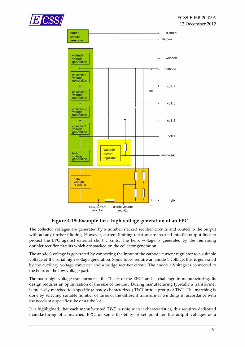
ECSS‐E‐HB‐20‐05A
12 December 2012
61
collector 4 voltage generation
cathode
coll. 4
collector 3 voltage generation
coll. 3
collector 2 voltage generation
coll. 2
collector 1 voltage generation
coll.1
helix voltage generation
helix voltage regulator
helix
helix currentmonitor
anode (A)
monitoranode voltage
heater voltage generation
filament
filament
wehnelt wehnelt voltage generation
cathode
currentregulator
Figure 4‐15: Example for a high voltage generation of an EPC
The collector voltages are generated by a number stacked rectifier circuits and routed to the output
without any further filtering. However, current limiting resistors are inserted into the output lines to
protect the EPC against external short circuits. The helix voltage is generated by the remaining
doubler rectifier circuits which are stacked on the collector generation.
The anode 0 voltage is generated by connecting the input of the cathode current regulator to a suitable
voltage of the serial high voltage generation. Some tubes require an anode 1 voltage; this is generated
by the auxiliary voltage converter and a bridge rectifier circuit. The anode 1 Voltage is connected to
the helix on the low voltage part.
The main high voltage transformer is the “heart of the EPC” and is challenge in manufacturing. Its
design requires an optimization of the size of the unit. During manufacturing typically a transformer
is precisely matched to a specific (already characterized) TWT or to a group of TWT. The matching is
done by selecting suitable number of turns of the different transformer windings in accordance with
the needs of a specific tube or a tube lot.
It is highlighted, that each manufactured TWT is unique in it characteristics, this requires dedicated
manufacturing of a matched EPC, or some flexibility of set point for the output voltages or a
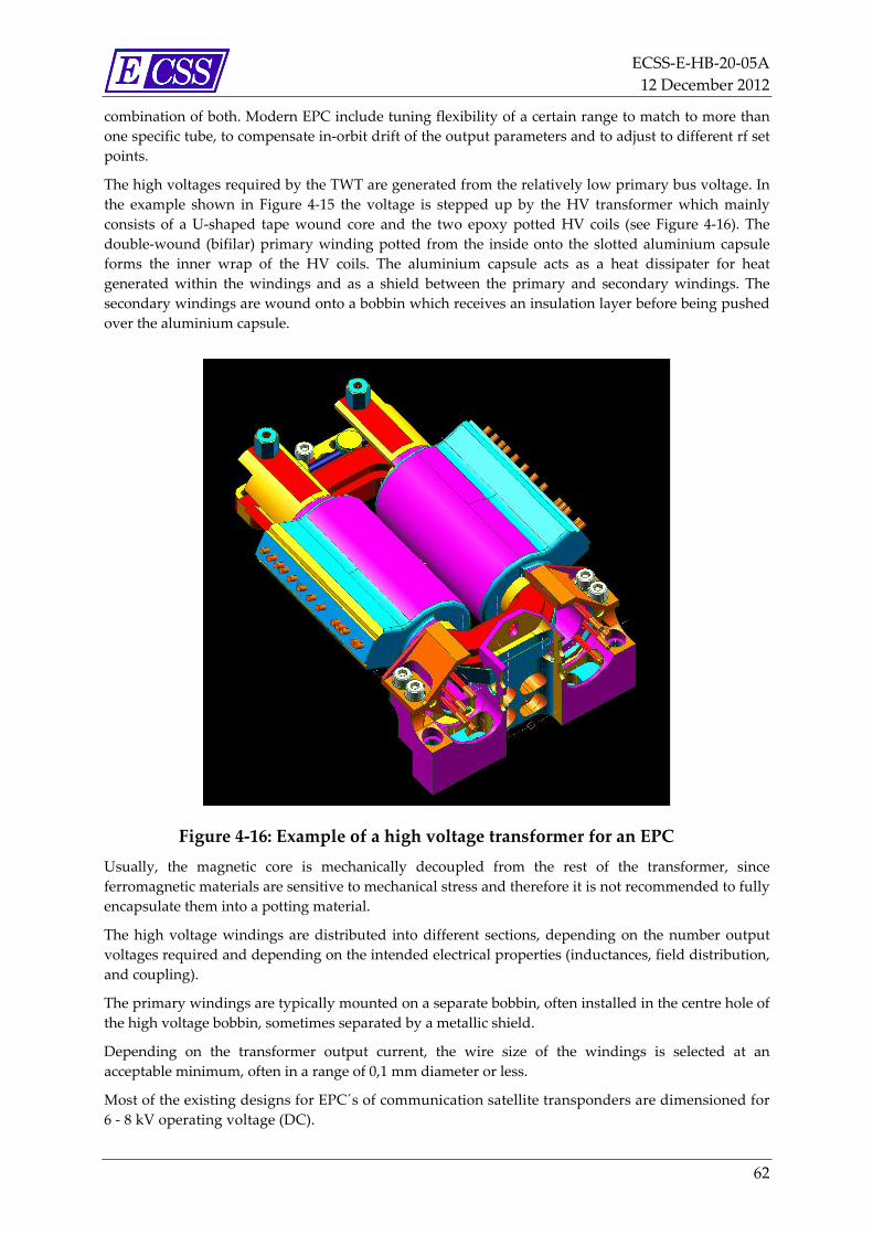
ECSS‐E‐HB‐20‐05A
12 December 2012
62
combination of both. Modern EPC include tuning flexibility of a certain range to match to more than
one specific tube, to compensate in‐orbit drift of the output parameters and to adjust to different rf set
points.
The high voltages required by the TWT are generated from the relatively low primary bus voltage. In
the example shown in Figure 4‐15 the voltage is stepped up by the HV transformer which mainly
consists of a U‐shaped tape wound core and the two epoxy potted HV coils (see Figure 4‐16). The
double‐wound (bifilar) primary winding potted from the inside onto the slotted aluminium capsule
forms the inner wrap of the HV coils. The aluminium capsule acts as a heat dissipater for heat
generated within the windings and as a shield between the primary and secondary windings. The
secondary windings are wound onto a bobbin which receives an insulation layer before being pushed
over the aluminium capsule.
Figure 4‐16: Example of a high voltage transformer for an EPC
Usually, the magnetic core is mechanically decoupled from the rest of the transformer, since
ferromagnetic materials are sensitive to mechanical stress and therefore it is not recommended to fully
encapsulate them into a potting material.
The high voltage windings are distributed into different sections, depending on the number output
voltages required and depending on the intended electrical properties (inductances, field distribution,
and coupling).
The primary windings are typically mounted on a separate bobbin, often installed in the centre hole of
the high voltage bobbin, sometimes separated by a metallic shield.
Depending on the transformer output current, the wire size of the windings is selected at an
acceptable minimum, often in a range of 0,1 mm diameter or less.
Most of the existing designs for EPC´s of communication satellite transponders are dimensioned for
6 ‐ 8 kV operating voltage (DC).
ECSS‐E‐HB‐20‐05A
12 December 2012
63
With a given voltage from a spacecraft power bus and specified voltage of the TWT load the ratio of
windings is globally given. The use of multiplier stages at the output and of boost converters at the
input can change this ratio, but there are limitations (i.e. efficiency) in use of these measures.
The number of turns of the windings is mainly determined by the core material and core cross section
(saturation, losses).
After optimization of the above parameters the “corner elements” of the transformer are defined:
cross section of the magnetic core hole
primary windings (turns, wire size)
secondary windings (sections, turns, wire size)
inner diameter(s) of the bobbin(s)
4.4.2.4 High Voltage Isolation Design of a Transformer
The insulating distances of the secondary windings are determined by the allowed electrical field
strength. Due to conservative recommendation the maximum field strengths should be limited to 6
kV/mm for DC‐fields and to 2 kV/mm for AC‐fields, although for many insulation materials the real
breakdown strengths are significantly higher.
In fact this means that for 8 kV DC operation voltage a minimum insulation distance of 1,3 mm is
needed, for 15 kV a distance of 2,5 mm is needed – for homogeneous fields(!).
In practice, the electrical field in transformer windings is not homogeneous – moreover at corners of
windings, thin wires, etc. the electrical field is enhanced. A field enhancement of 5 is allowed, but still
under the condition, that max. field strength values are not exceeded. Therefore, the insulation
thickness should be further increased.
It is highlighted, that an increase of the insulation distance should be done on both sides of the
winding – for radial configurations the diameter increases by a factor of 4 (rule of thumb). In axial
directions the insulation increase depends on the configuration of the section, but in worst cases, the
high voltage levels can increase by a factor 2 (rule of thumb).
A further mass penalty arises with the increasing diameter of the bobbins and its high voltage
insulation: the magnetic core has to provide a closed loop through the centre of the bobbins. With
growing bobbin size a larger magnetic core should be used. As a consequence an additional (iron)
mass adds to the mass budget.
Detailed optimization typically involves numerical field calculations by Finite Elements software (or
similar) as shown in Figure 4‐17.
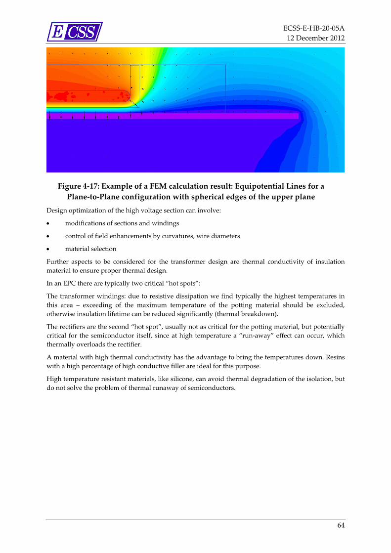
ECSS‐E‐HB‐20‐05A
12 December 2012
64
Figure 4‐17: Example of a FEM calculation result: Equipotential Lines for a
Plane‐to‐Plane configuration with spherical edges of the upper plane
Design optimization of the high voltage section can involve:
modifications of sections and windings
control of field enhancements by curvatures, wire diameters
material selection
Further aspects to be considered for the transformer design are thermal conductivity of insulation
material to ensure proper thermal design.
In an EPC there are typically two critical “hot spots”:
The transformer windings: due to resistive dissipation we find typically the highest temperatures in
this area – exceeding of the maximum temperature of the potting material should be excluded,
otherwise insulation lifetime can be reduced significantly (thermal breakdown).
The rectifiers are the second “hot spot”, usually not as critical for the potting material, but potentially
critical for the semiconductor itself, since at high temperature a “run‐away” effect can occur, which
thermally overloads the rectifier.
A material with high thermal conductivity has the advantage to bring the temperatures down. Resins
with a high percentage of high conductive filler are ideal for this purpose.
High temperature resistant materials, like silicone, can avoid thermal degradation of the isolation, but
do not solve the problem of thermal runaway of semiconductors.
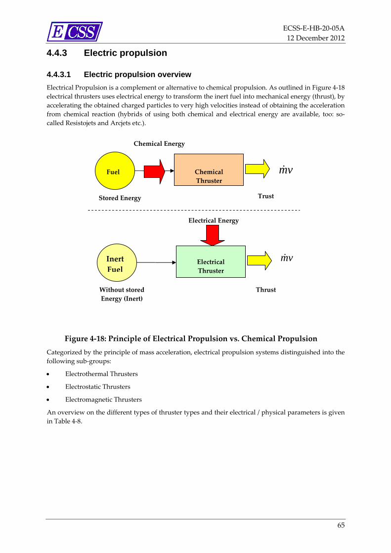
ECSS‐E‐HB‐20‐05A
12 December 2012
65
4.4.3 Electric propulsion
4.4.3.1 Electric propulsion overview
Electrical Propulsion is a complement or alternative to chemical propulsion. As outlined in Figure 4‐18
electrical thrusters uses electrical energy to transform the inert fuel into mechanical energy (thrust), by
accelerating the obtained charged particles to very high velocities instead of obtaining the acceleration
from chemical reaction (hybrids of using both chemical and electrical energy are available, too: so‐
called Resistojets and Arcjets etc.).
Figure 4‐18: Principle of Electrical Propulsion vs. Chemical Propulsion
Categorized by the principle of mass acceleration, electrical propulsion systems distinguished into the
following sub‐groups:
Electrothermal Thrusters
Electrostatic Thrusters
Electromagnetic Thrusters
An overview on the different types of thruster types and their electrical / physical parameters is given
in Table 4‐8.
Chemical
Thruster
Fuel vm
Electrical
Thruster
Inert
Fuel
vm
Stored Energy
Without stored
Energy (Inert)
Electrical Energy
Chemical Energy
Trust
Thrust

ECSS‐E‐HB‐20‐05A
12 December 2012
66
Table 4‐8: Overview on Electrical Propulsion Principles, Thruster Type and
Electrical Physical Parameters
Principle Fuel Voltage
(Main Power)
Power Specific Impulse Efficiency Thrust
Electrothermal
Resistojet Ammonia,
Argon, N2,
Xe
few volts 0,5 ‐ 1,5 kW 300 s 80 %
Arcjet Hydrazine,
Ammonia,
Argon, H2
> 1 kV ignition
few V operation
0,3 ‐ 100 kW 500 ‐ 2000 s 35 %
Electrostatic
Ion Xenon 1 ‐ 2 kV 0,5 ‐ 5 kW 3000 ‐ 5000 s 60‐80 % 10 ‐ 200 mN
Plasma ‐ Hall Xenon 0,3 ‐ 0,8 kV 1,5 ‐ 5 kW 1500 ‐ 2000 s 50 % 80 ‐ 400 mN
Plasma ‐ HEMP Xenon 1‐2 kV 0,5 ‐ 1 kW 2000 ‐ 3000 s 60‐70 % 40 ‐ 200 mN
FEEP Indium,
Cesium
5 ‐ 15 kV 10 ‐ 150 W 8000 ‐ 12000 s 30‐90 % 0,001 ‐ 1 mN
Colloid Glycerol,
ionic liquids
2 ‐ 5 kV 5 ‐ 50 W 500 ‐ 1500 s 60‐90 % 0,001 ‐ 1 mN
Electromagnetic
Pulsed Plasma Teflon > 15 kV ignistion
few kV operation
1 ‐ 200 W 10000 s 5 % 1 ‐ 100 mN
Magnetoplasma‐
dynamic
Ammonia,
H2
> 1 kV ignistion
few 10 V
operation
1 ‐ 4000 kW 2000 ‐ 5000 s 25 % 1 ‐ 200 N
Variable ISP
Plasma Rocket
H2 1 ‐ 10 MW 3000 ‐ 30000 s < 60 % 1 ‐ 2 kN
Typically an Electric propulsion (EP) system consists of one or more electrical thrusters connected to a
power supply and (except for FEEP, colloid and pulsed plasma thrusters) to a gas feed system. The
electric power supply unit of an EP system is typically called PPU (Power Processing Unit), PSCU
(Power Supply and Control Unit) or simply PCU (Power Control Unit) and is providing various high
voltage lines, heater lines and complex control functions to the thrusters.
The following discussion is focused mainly on the used or close to use (going to qualification) EP
thruster principles, which are:
FEEP (Field Emission Electric Propulsion) Thruster
Plasma Thrusters (Hall effect type)
Plasma Thrusters (HEMP type)
Ion Engines (Ion Thrusters) ‐ Kaufmann type
Ion Engines (Ion Thrusters) ‐ (Radio‐frequency type
FEEP utilizes the field emission of metallic ions from a liquid metal surface, so there, the propellant
being either Indium or Caesium. The plasma thrusters (Hall and HEMP) and ion engines all use
Xenon gas as a propellant. The gas is ionized and the Xenon ions are accelerated, both ionization and
acceleration are based on different principles depending on the thruster type.
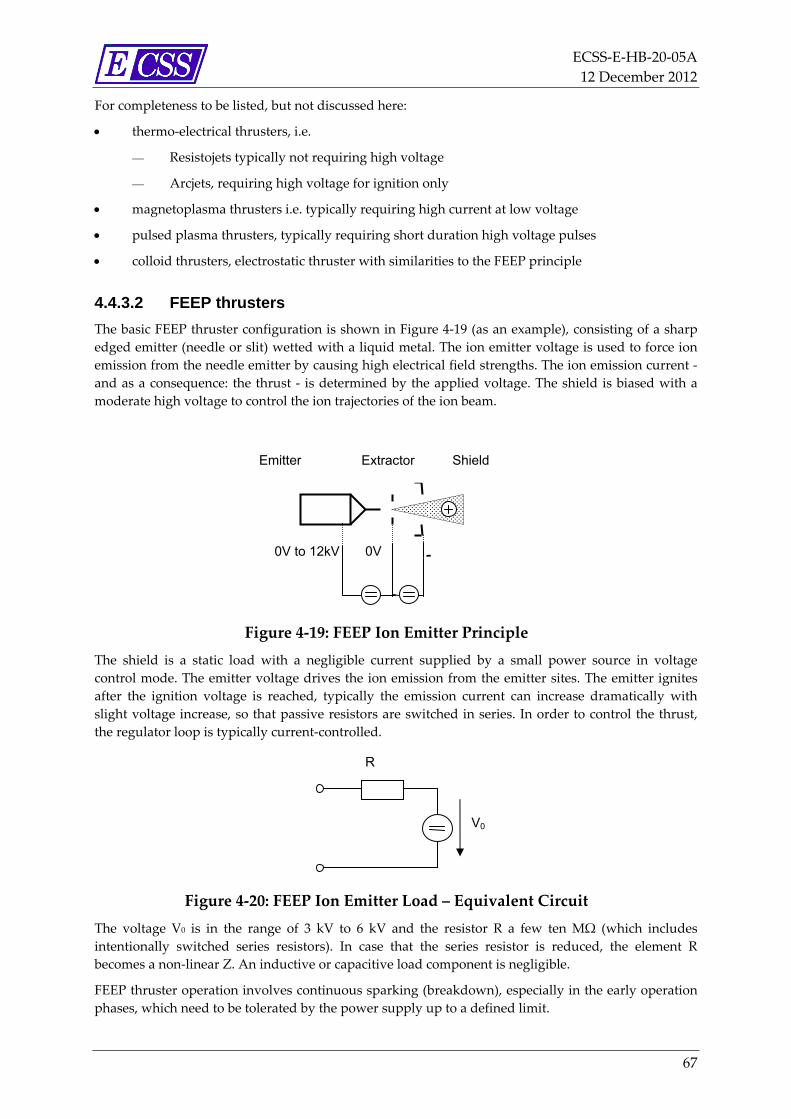
ECSS‐E‐HB‐20‐05A
12 December 2012
67
For completeness to be listed, but not discussed here:
thermo‐electrical thrusters, i.e.
Resistojets typically not requiring high voltage
Arcjets, requiring high voltage for ignition only
magnetoplasma thrusters i.e. typically requiring high current at low voltage
pulsed plasma thrusters, typically requiring short duration high voltage pulses
colloid thrusters, electrostatic thruster with similarities to the FEEP principle
4.4.3.2 FEEP thrusters
The basic FEEP thruster configuration is shown in Figure 4‐19 (as an example), consisting of a sharp
edged emitter (needle or slit) wetted with a liquid metal. The ion emitter voltage is used to force ion
emission from the needle emitter by causing high electrical field strengths. The ion emission current ‐
and as a consequence: the thrust ‐ is determined by the applied voltage. The shield is biased with a
moderate high voltage to control the ion trajectories of the ion beam.
Figure 4‐19: FEEP Ion Emitter Principle
The shield is a static load with a negligible current supplied by a small power source in voltage
control mode. The emitter voltage drives the ion emission from the emitter sites. The emitter ignites
after the ignition voltage is reached, typically the emission current can increase dramatically with
slight voltage increase, so that passive resistors are switched in series. In order to control the thrust,
the regulator loop is typically current‐controlled.
Figure 4‐20: FEEP Ion Emitter Load – Equivalent Circuit
The voltage V0 is in the range of 3 kV to 6 kV and the resistor R a few ten MΩ (which includes
intentionally switched series resistors). In case that the series resistor is reduced, the element R
becomes a non‐linear Z. An inductive or capacitive load component is negligible.
FEEP thruster operation involves continuous sparking (breakdown), especially in the early operation
phases, which need to be tolerated by the power supply up to a defined limit.
V0
R
Extractor Emitter Shield
‐0V to 12kV 0V
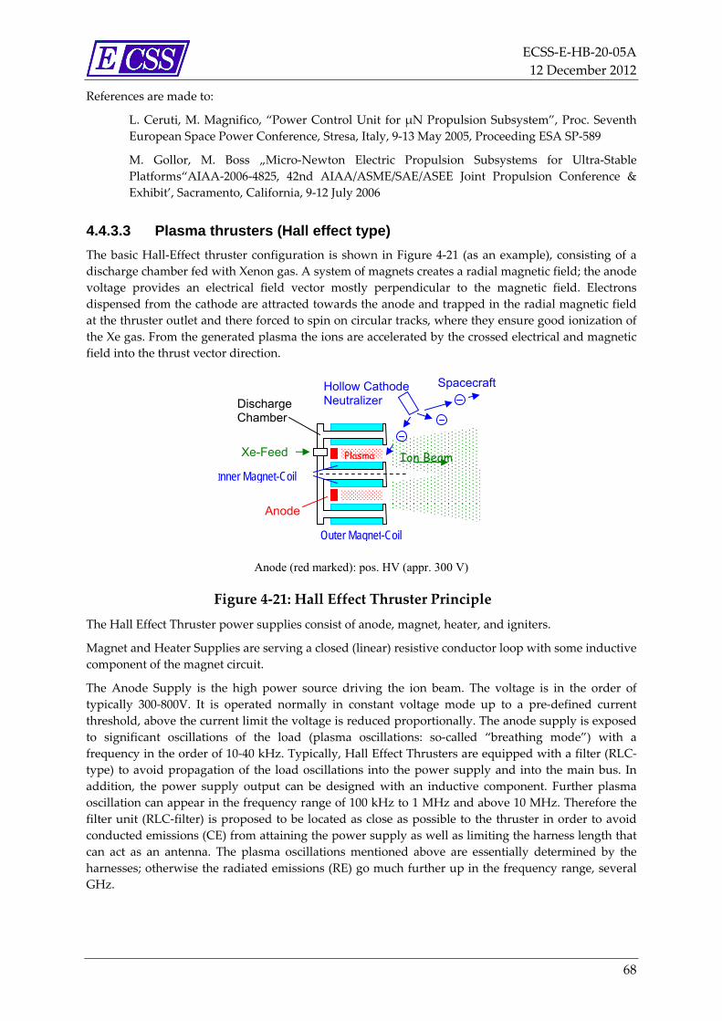
ECSS‐E‐HB‐20‐05A
12 December 2012
68
References are made to:
L. Ceruti, M. Magnifico, “Power Control Unit for μN Propulsion Subsystem”, Proc. Seventh
European Space Power Conference, Stresa, Italy, 9‐13 May 2005, Proceeding ESA SP‐589
M. Gollor, M. Boss „Micro‐Newton Electric Propulsion Subsystems for Ultra‐Stable
Platforms“AIAA‐2006‐4825, 42nd AIAA/ASME/SAE/ASEE Joint Propulsion Conference &
Exhibit’, Sacramento, California, 9‐12 July 2006
4.4.3.3 Plasma thrusters (Hall effect type)
The basic Hall‐Effect thruster configuration is shown in Figure 4‐21 (as an example), consisting of a
discharge chamber fed with Xenon gas. A system of magnets creates a radial magnetic field; the anode
voltage provides an electrical field vector mostly perpendicular to the magnetic field. Electrons
dispensed from the cathode are attracted towards the anode and trapped in the radial magnetic field
at the thruster outlet and there forced to spin on circular tracks, where they ensure good ionization of
the Xe gas. From the generated plasma the ions are accelerated by the crossed electrical and magnetic
field into the thrust vector direction.
Anode (red marked): pos. HV (appr. 300 V)
Figure 4‐21: Hall Effect Thruster Principle
The Hall Effect Thruster power supplies consist of anode, magnet, heater, and igniters.
Magnet and Heater Supplies are serving a closed (linear) resistive conductor loop with some inductive
component of the magnet circuit.
The Anode Supply is the high power source driving the ion beam. The voltage is in the order of
typically 300‐800V. It is operated normally in constant voltage mode up to a pre‐defined current
threshold, above the current limit the voltage is reduced proportionally. The anode supply is exposed
to significant oscillations of the load (plasma oscillations: so‐called “breathing mode”) with a
frequency in the order of 10‐40 kHz. Typically, Hall Effect Thrusters are equipped with a filter (RLC‐
type) to avoid propagation of the load oscillations into the power supply and into the main bus. In
addition, the power supply output can be designed with an inductive component. Further plasma
oscillation can appear in the frequency range of 100 kHz to 1 MHz and above 10 MHz. Therefore the
filter unit (RLC‐filter) is proposed to be located as close as possible to the thruster in order to avoid
conducted emissions (CE) from attaining the power supply as well as limiting the harness length that
can act as an antenna. The plasma oscillations mentioned above are essentially determined by the
harnesses; otherwise the radiated emissions (RE) go much further up in the frequency range, several
GHz.
Xe-Feed
Outer Magnet-Coil
Hollow Cathode Neutralizer
Plasma Ion Beam
Anode
Discharge Chamber
Inner Magnet-Coil
Spacecraft
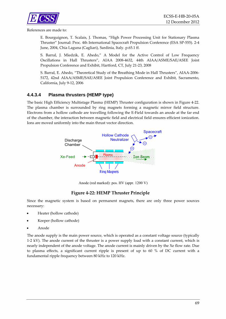
ECSS‐E‐HB‐20‐05A
12 December 2012
69
References are made to:
E. Bourguignon, T. Scalais, J. Thomas, “High Power Processing Unit for Stationary Plasma
Thruster” Journal: Proc. 4th International Spacecraft Propulsion Conference (ESA SP‐555). 2‐4
June, 2004, Chia Laguna (Cagliari), Sardinia, Italy. p.65.1 ff.
S. Barral, J. Miedzik, E. Ahedo,” A Model for the Active Control of Low Frequency
Oscillations in Hall Thrusters”, AIAA 2008‐4632, 44th AIAA/ASME/SAE/ASEE Joint
Propulsion Conference and Exhibit, Hartford, CT, July 21‐23, 2008
S. Barral, E. Ahedo, “Theoretical Study of the Breathing Mode in Hall Thrusters”, AIAA‐2006‐
5172, 42nd AIAA/ASME/SAE/ASEE Joint Propulsion Conference and Exhibit, Sacramento,
California, July 9‐12, 2006
4.4.3.4 Plasma thrusters (HEMP type)
The basic High Efficiency Multistage Plasma (HEMP) Thruster configuration is shown in Figure 4‐22.
The plasma chamber is surrounded by ring magnets forming a magnetic mirror field structure.
Electrons from a hollow cathode are travelling following the E‐Field towards an anode at the far end
of the chamber, the interaction between magnetic field and electrical field ensures efficient ionization.
Ions are moved uniformly into the main thrust vector direction.
Anode (red marked): pos. HV (appr. 1200 V)
Figure 4‐22: HEMP Thruster Principle
Since the magnetic system is based on permanent magnets, there are only three power sources
necessary:
Heater (hollow cathode)
Keeper (hollow cathode)
Anode
The anode supply is the main power source, which is operated as a constant voltage source (typically
1‐2 kV). The anode current of the thruster is a power supply load with a constant current, which is
nearly independent of the anode voltage. The anode current is mainly driven by the Xe flow rate. Due
to plasma effects, a significant current ripple is present of up to 60 % of DC current with a
fundamental ripple frequency between 80 kHz to 120 kHz.
Xe-Feed
Hollow CathodeNeutralizer
Plasma Ion Beam
Anode
Discharge Chamber
Ring Magnets
Spacecraft
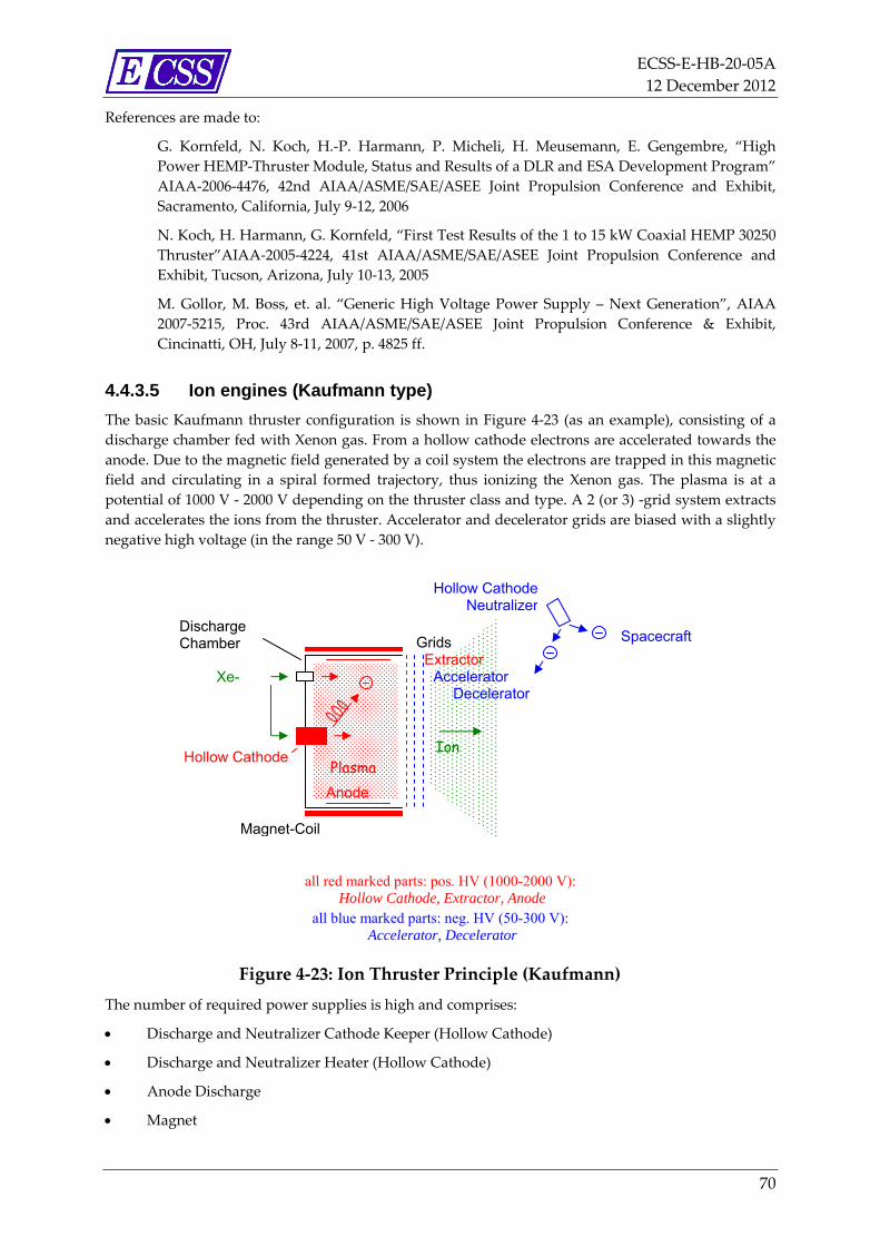
ECSS‐E‐HB‐20‐05A
12 December 2012
70
References are made to:
G. Kornfeld, N. Koch, H.‐P. Harmann, P. Micheli, H. Meusemann, E. Gengembre, “High
Power HEMP‐Thruster Module, Status and Results of a DLR and ESA Development Program”
AIAA‐2006‐4476, 42nd AIAA/ASME/SAE/ASEE Joint Propulsion Conference and Exhibit,
Sacramento, California, July 9‐12, 2006
N. Koch, H. Harmann, G. Kornfeld, “First Test Results of the 1 to 15 kW Coaxial HEMP 30250
Thruster”AIAA‐2005‐4224, 41st AIAA/ASME/SAE/ASEE Joint Propulsion Conference and
Exhibit, Tucson, Arizona, July 10‐13, 2005
M. Gollor, M. Boss, et. al. “Generic High Voltage Power Supply – Next Generation”, AIAA
2007‐5215, Proc. 43rd AIAA/ASME/SAE/ASEE Joint Propulsion Conference & Exhibit,
Cincinatti, OH, July 8‐11, 2007, p. 4825 ff.
4.4.3.5 Ion engines (Kaufmann type)
The basic Kaufmann thruster configuration is shown in Figure 4‐23 (as an example), consisting of a
discharge chamber fed with Xenon gas. From a hollow cathode electrons are accelerated towards the
anode. Due to the magnetic field generated by a coil system the electrons are trapped in this magnetic
field and circulating in a spiral formed trajectory, thus ionizing the Xenon gas. The plasma is at a
potential of 1000 V ‐ 2000 V depending on the thruster class and type. A 2 (or 3) ‐grid system extracts
and accelerates the ions from the thruster. Accelerator and decelerator grids are biased with a slightly
negative high voltage (in the range 50 V ‐ 300 V).
all red marked parts: pos. HV (1000-2000 V): Hollow Cathode, Extractor, Anode
all blue marked parts: neg. HV (50-300 V): Accelerator, Decelerator
Figure 4‐23: Ion Thruster Principle (Kaufmann)
The number of required power supplies is high and comprises:
Discharge and Neutralizer Cathode Keeper (Hollow Cathode)
Discharge and Neutralizer Heater (Hollow Cathode)
Anode Discharge
Magnet
Xe-
Magnet-Coil
Grids Extractor Accelerator Decelerator
Hollow Cathode Plasma
Ion
Anode
Discharge Chamber
Hollow CathodeNeutralizer
Spacecraft
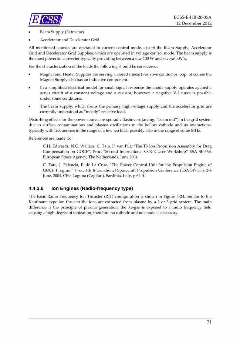
ECSS‐E‐HB‐20‐05A
12 December 2012
71
Beam Supply (Extractor)
Accelerator and Decelerator Grid
All mentioned sources are operated in current control mode, except the Beam Supply, Accelerator
Grid and Decelerator Grid Supplies, which are operated in voltage control mode. The beam supply is
the most powerful converter typically providing between a few 100 W and several kW´s.
For the characterization of the loads the following should be considered:
Magnet and Heater Supplies are serving a closed (linear) resistive conductor loop; of course the
Magnet Supply also has an inductive component.
In a simplified electrical model for small signal response the anode supply operates against a
series circuit of a constant voltage and a resistor, however, a negative V‐I curve is possible
under some conditions.
The beam supply, which forms the primary high voltage supply and the accelerator grid are
currently understood as “mostly” resistive load.
Disturbing effects for the power source are sporadic flashovers (arcing, “beam out”) in the grid system
due to surface contaminations and plasma oscillations in the hollow cathode and its interactions,
typically with frequencies in the range of a few ten kHz, possibly also in the range of some MHz.
References are made to:
C.H. Edwards, N.C. Wallace, C. Tato, P. van Put, “The T5 Ion Propulsion Assembly for Drag
Compensation on GOCE”, Proc. “Second International GOCE User Workshop” ESA SP‐569,
European Space Agency, The Netherlands, June 2004
C. Tato, J. Palencia, F. de La Cruz, “The Power Control Unit for the Propulsion Engine of
GOCE Program” Proc. 4th International Spacecraft Propulsion Conference (ESA SP‐555). 2‐4
June, 2004, Chia Laguna (Cagliari), Sardinia, Italy. p.64 ff.
4.4.3.6 Ion Engines (Radio-frequency type)
The basic Radio Frequency Ion Thruster (RIT) configuration is shown in Figure 4‐24. Similar to the
Kaufmann type ion thruster the ions are extracted from plasma by a 2 or 3 grid system. The main
difference is the principle of plasma generation: the Xe‐gas is exposed to a radio frequency field
causing a high degree of ionization, therefore no cathode and no anode is necessary.

ECSS‐E‐HB‐20‐05A
12 December 2012
72
all red marked parts: pos. HV (1000‐2000 V):
Extractor
all blue marked parts: neg. HV (0‐300 V):
Accelerator, Decelerator
Figure 4‐24: Radio Frequency Ion Thruster (RIT) Principle
The RF coil supply is a combination of a DC voltage regulator and followed by an active RF oscillator
(700‐1000 kHz). The grids are supplied by voltage controlled positive and negative high voltage
sources, whereas the positive high voltage takes the main power load. The ion flow and therefore the
load of the positive high voltage source are depending on the RF power fed into the plasma. As a
consequence, the beam current is nearly constant (slightly increasing) over a wide range of extractor
voltage.
Disturbing effects for the power source are sporadic flashovers (arcing, “beam out”) in the grid system
due to surface contaminations.
References are made to:
S. Arcisto, M. Gambarara, A. Garutti, A. Trivulzio, A. Truffi, H. Bassner, H. Mueller, “Power
supply and control unit (PCSU) for radio frequency ion thrusters (RIT)” ESA, Proc. 2nd
European Spacecraft Propulsion, Noordwijk, The Netherlands, 27‐29 May 1997 (ESA SP‐398),
pp 643‐648
H. Leiter, R. Killinger, M. Boss, M. Braeg, M. Gollor, S. Weis, D. Feili, M. Tartz, H. Neumann,
D. di Cara, ”RIT‐μX ‐ High Precision Micro Ion Propulsion System Based on RF‐Technology”
AIAA 2007‐5250 43rd AIAA/ASME/SAE/ASEE Joint Propulsion Conference and Exhibit,
Cincinnati, OH, July 8‐11, 2007
4.4.4 Microwave tubes
Microwave tubes are used in for RF signal amplification in terrestrial and for space applications,
especially in cases where high RF power levels of several ten watts or higher are needed. For space
applications some relevant examples are given in the following:
220 W –S‐band –67 % efficiency (TWT)
220 W –Ku‐band –67 % efficiency (TWT)
130 W –Ka‐band –65 % efficiency (TWT)
5,5 kW –C‐band –pulsed (TWT)
1,6 kW –W‐band –pulsed (Extended Interaction Klystron).
Xe-Feed
RF-Coil
Grids Extractor Accelerator Decelerator
Plasma
Ion Beam
Discharge Chamber
Hollow CathodeNeutralizer
Spacecraft
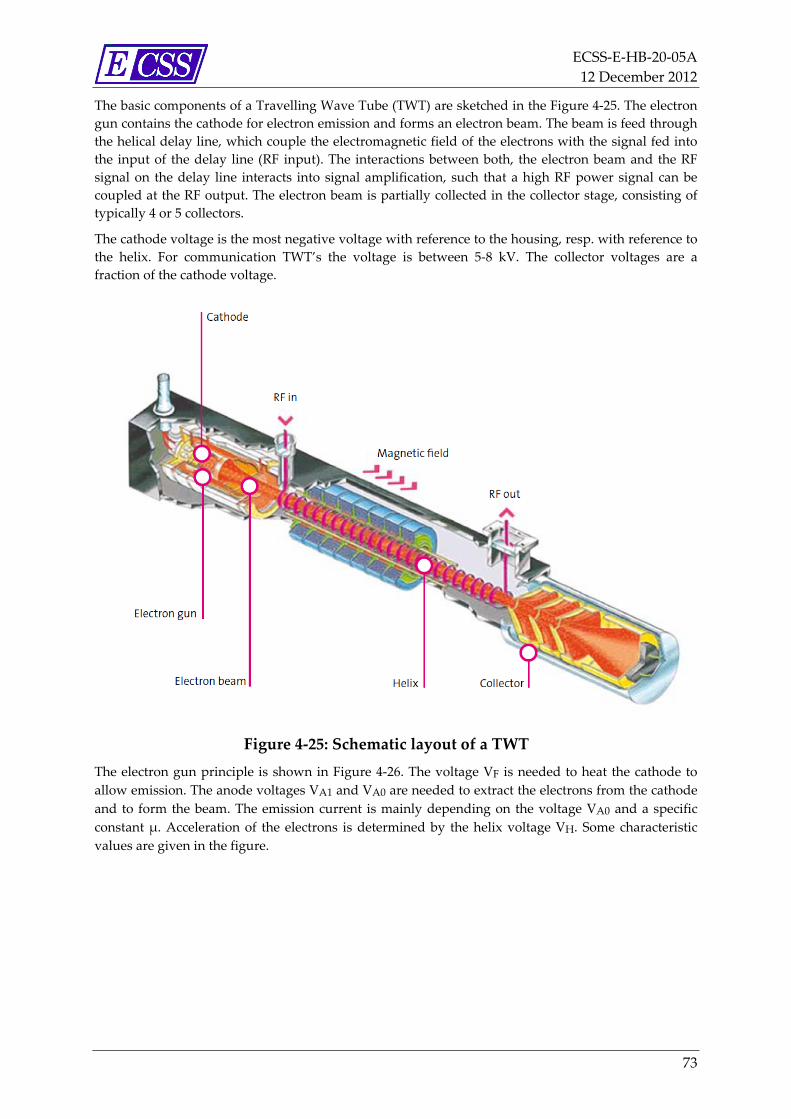
ECSS‐E‐HB‐20‐05A
12 December 2012
73
The basic components of a Travelling Wave Tube (TWT) are sketched in the Figure 4‐25. The electron
gun contains the cathode for electron emission and forms an electron beam. The beam is feed through
the helical delay line, which couple the electromagnetic field of the electrons with the signal fed into
the input of the delay line (RF input). The interactions between both, the electron beam and the RF
signal on the delay line interacts into signal amplification, such that a high RF power signal can be
coupled at the RF output. The electron beam is partially collected in the collector stage, consisting of
typically 4 or 5 collectors.
The cathode voltage is the most negative voltage with reference to the housing, resp. with reference to
the helix. For communication TWT’s the voltage is between 5‐8 kV. The collector voltages are a
fraction of the cathode voltage.
Figure 4‐25: Schematic layout of a TWT
The electron gun principle is shown in Figure 4‐26. The voltage VF is needed to heat the cathode to
allow emission. The anode voltages VA1 and VA0 are needed to extract the electrons from the cathode
and to form the beam. The emission current is mainly depending on the voltage VA0 and a specific
constant μ. Acceleration of the electrons is determined by the helix voltage VH. Some characteristic
values are given in the figure.
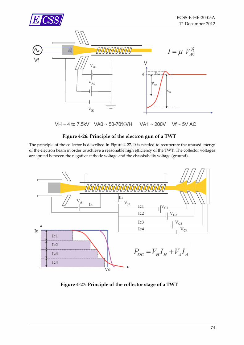
ECSS‐E‐HB‐20‐05A
12 December 2012
74
Figure 4‐26: Principle of the electron gun of a TWT
The principle of the collector is described in Figure 4‐27. It is needed to recuperate the unused energy
of the electron beam in order to achieve a reasonable high efficiency of the TWT. The collector voltages
are spread between the negative cathode voltage and the chassis/helix voltage (ground).
Figure 4‐27: Principle of the collector stage of a TWT
ECSS‐E‐HB‐20‐05A
12 December 2012
75
From the point of high voltage insulation and design, the most relevant parts are the
insulators/spacers, which fix the internal structures operated at high voltage potential. Furthermore,
the high voltage feedthroughs from the vacuum inside the tube towards the ambient outside are the
major aspects of the high voltage insulation.
Most of the internal insulators and the feedthroughs are made of ceramics in order to ensure a high
quality vacuum inside of the tube. High voltage cables are connected externally to the ceramic high
voltage feedthroughs. Typical high voltage cables used for TWTs are made of PTFE or FEP, in some
cases silicon rubber insulation is used. Often the high wires are potted in the area of the ceramic
feedthroughs by silicone rubber materials. Especially the temperatures of the collector are high due to
the dissipation.
A special electrical breakdown phenomenon related to the presence of high electrical RF fields can
occur in the RF high power conductors (waveguide) and is the so‐called multipaction phenomenon.
For details see ECSS‐E‐20‐01A (Multipaction design and test standard).
4.4.5 Scientific instruments and experiments Very specific applications for high voltage equipments exist in the field of scientific experiments and
instruments. As this field is very wide, the needed power levels and characteristics are very
heterogeneous. For an overview a course classification and description is given in the following:
Laser Instruments
Plasma Measurement Instruments
Radiation and Particle Measurements Instruments
Fluid Science Experiments
Laser Instruments are involving high voltage in two different ways: for the generation of a high power
laser beam and for switched in the optical path. High power lasers have been studied for ESA
missions with gas laser concepts (CO2 lasers) using pulse voltage up to 150 kV for 10μs pulse length
and 10 Hz repetition rate on breadboard study level. Optical Q‐switches based on the Kerr‐Effect
principle use high voltage to change orientation of optical polarisation if optical crystals. These
switches need fast change of a high voltage of 3‐10 kV with rise/fall times in the nanosecond range. Q‐
switch drivers are often formed by a static DC power supply feeding into a high voltage push‐pull
stage. As the voltage ratings of semiconductor switches are limited, the high voltage push‐pull stage is
formed by an array of transistors switched in series. Gate signal drive is isolated via capacitive or
transformer coupling. Related technologies have been developed for flight as part of the ESA Aladin
(Earthcare mission) instrument and of the ESA ATLID instrument (Aelous mission).
Plasma Measurement Instruments are used to analyse various types of space plasma. Therefore
typically a high voltage is applied between a set of electrodes. These electrodes are exposed to the free
space and the “leakage” current through existing plasma is measured. The required voltages vary
depending on the type and density of the investigated plasma from the range of a few hundred volts
to a few kilovolts, DC, AC or with modulations. As currents are typically low in the nA or μA‐range
high voltages are often generated by high voltage multipliers as described in section 4.4.1. A reference
is made to EFI instrument of the ESA Swarm Mission
Radiation and Particle Measurements Instruments detect charge generation caused by radiation or fast
particles. These generated charges result into a current pulse when a high voltage field is applied by
suitable electrodes. The needed high voltages are in the range of a few kilovolt up to the range of
about 30 kV with low currents in the nA or μA‐range. High voltages are often generated by high
voltage multipliers as described in section 4.4.1. A reference is made to ESA Cluster mission and ESA
Integral mission.

ECSS‐E‐HB‐20‐05A
12 December 2012
76
There have been flown a number of Fluid Science experiments on manned space missions for in‐flight
zero‐gravity research using unique high voltages, here to mention:
BDPU Bubble, Drop & Particle Experiment for Material Science Lab (ESA / Space Lab)
Columbus FASES GEOFLOW onboard ISS (ESA)
Both experiments required high frequency ac high voltage with adjustable amplitude up to 15 kV‐
peak‐to‐peak. For BDPU the amplitude, the waveform and the frequency were adjustable, for
GEOFLOW only the amplitude.
ECSS‐E‐HB‐20‐05A
12 December 2012
77
5 High voltage design principles
5.1 Basic design principles Reliable high voltage design is based on principles avoiding a breakdown of the electrical insulation.
These basic principles are the
control of voltage
control of electrical field strengths
control of electrical field distributions
control of partial discharges
control of triple junction effects
control of interferences
Most of the mentioned basis principles are linked to each other. Not all are relevant for all
applications, however, all points should be checked for there relevance and their fulfilment. More
explanations are given in the following sections.
5.1.1 Control of voltage The typical destruction process is involving acceleration of electrons (in some cases ions) and its
collision with matter. The maximum energy of an electron accelerated by an electrical field in a free
path is given by the basic equation:
UeWkin [5‐1]
where:
Wkin kinetic energy
e electron charge
U voltage
A collision of an accelerated electron with atom and ions can only be relevant for an electrical
breakdown, if a certain kinetic energy is reached to cause displacements and ionization. As a
simplified conclusion it can be deducted, that below a specific voltage threshold there is no specific
high voltage related breakdown mechanism possible (to be distinguished from other – non‐voltage
related failure mechanisms).
The definition of a general threshold voltage is difficult as there are different insulation scenarios to be
considered. Table 5‐1 gives an overview of some critical high voltage related “thresholds”.
ECSS‐E‐HB‐20‐05A
12 December 2012
78
Table 5‐1: Critical “thresholds” for high voltage
Gaseous insulation with low pressure
ambient atmosphere (air)
transition from ambient atmosphere into space
“bad” space environment due to gas leakages and outgassing
> 90 V
Paschen Breakdown in pure inert gas (Ar) atmosphere
possible *)
> 240 V
Paschen Breakdown in pure nitrogen (N2) atmosphere
possible *)
> 330 V Paschen Breakdown in air (N2) possible *)
General for space applications
> 200 V **) electrical insulation becomes a design driver
Safety relevant
> 60 V DC hazardous voltage ***)
> 25 V AC hazardous voltage ***)
*) see section 4.3.4 and 5.1.7 **) tentatively ***) see section 9
As a general guideline the following voltage levels can be critical with respect to high voltage related
phenomena and can require specific design precautions:
Voltage > 200 V
in general
Voltage > 90V
in specific low pressure gaseous environment
Voltages < 90 V
in specific cases for example if plasma and charging generated by external “source” (space
plasma, ionizing source, electrical arcs etc.). This can potentially create conditions for an
electrical breakdown even under low voltage. This should be taken into account at least for
structures on the outer surface of a spacecraft (for example: solar generators).
NOTE High voltage breakdown develops in a timeframe of a few
nanoseconds up to a few microseconds. Thus, for the final
breakdown voltage always the peak value of an AC or pulse
voltage is the design driver for the electrical insulation.
ECSS‐E‐HB‐20‐05A
12 December 2012
79
5.1.2 Control of electrical field strengths
5.1.2.1 Electrical Field Strengths Classifications
The electrical field is caused by an electrical potential. In the typical technical high voltage
applications under consideration here, an applied electrical voltage across an insulating space results
in an electrical field. The resulting electrical field can be a
Uniform electrical field:
the resulting electrical field strengths is constant in all locations of the insulating gap
Non‐Uniform electrical field:
the resulting electrical field strengths varies depending on the locations in the insulating gap
Important for the characterization of an electrical field are the following field parameters:
Maximum electrical field strength: maxE
the maximum value of the electrical field strengths in the insulating gap
Mean electrical field strength: meanE (or E )
the mean value of the electrical field strengths in the insulating gap
Electrical field enhancement factor:
the ratio of maximum electrical field strengths to mean electrical field strength
meanEEmax [5‐2]
Calculation methods and examples are given in section 5.1.2.9.
The most important parameter driving electrical breakdown of insulation is
the maximum electrical field strength maxE
since typically, in the zone of the maximum electrical field strength, discharges (and partial
discharges) start triggering immediate or produce erosive breakdown.
As insulation typically is optimized to minimize size and mass of high voltage equipment, the
electrical field enhancement factor should be minimized to get an optimum distribution of the
electrical field, which means a very uniform field (see section 5.1.3).
If the maximum electrical field strength maxE is not kept below the electrical breakdown field strength
dE of the insulation material an electrical breakdown would occur:
dEE max .
In practice the value of electrical breakdown field strengths dE depends on:
the applied profile of stress
Alternating voltages (AC) causing polarity change of electrical fields lead to significantly lower
electrical breakdown field strengths, than pure DC voltage (resp.) or combined DC+AC stress or
pulse stressed.
Long‐term effects
Long‐term electrical breakdown field strengths (hours, months, years) is significantly lower
than short term strengths (minutes, seconds and below).
ECSS‐E‐HB‐20‐05A
12 December 2012
80
Table 5‐2 gives an orientation for maximum electrical field strengths typically used in high voltage
applications (for space):
Table 5‐2: Orientation “map” for maximum electrical field strengths in electrical
insulation
Max. electrical
field strength:
maxETypical safe operating range Remark
1 ‐ 2 kV/mm Air (ambient)
5 ‐ 8 kV/mm high insulating and pressurized
gaseous insulation (SF6)
0,5 ‐ 2 kV/mm solid insulating material (AC voltage)
1 ‐ 10 kV/mm solid insulating material (DC voltage)
5 ‐ 20 kV/mm thin layers of solid insulating material
(i.e. dielectrics of capacitors)
0,3 ‐ 0,6 kV/mm solid insulation creepage path
1 ‐ 10 kV/mm vacuum insulation
5.1.2.2 General control means for electrical field strength
The electrical field strength is dependent on:
Voltage
Geometrical parameters:
Distance (Insulator/Gap lengths)
Shape
Dielectric properties (in conjunction with geometry)
Specific insulation resistance
Dielectric constant r
Space charges / Potential
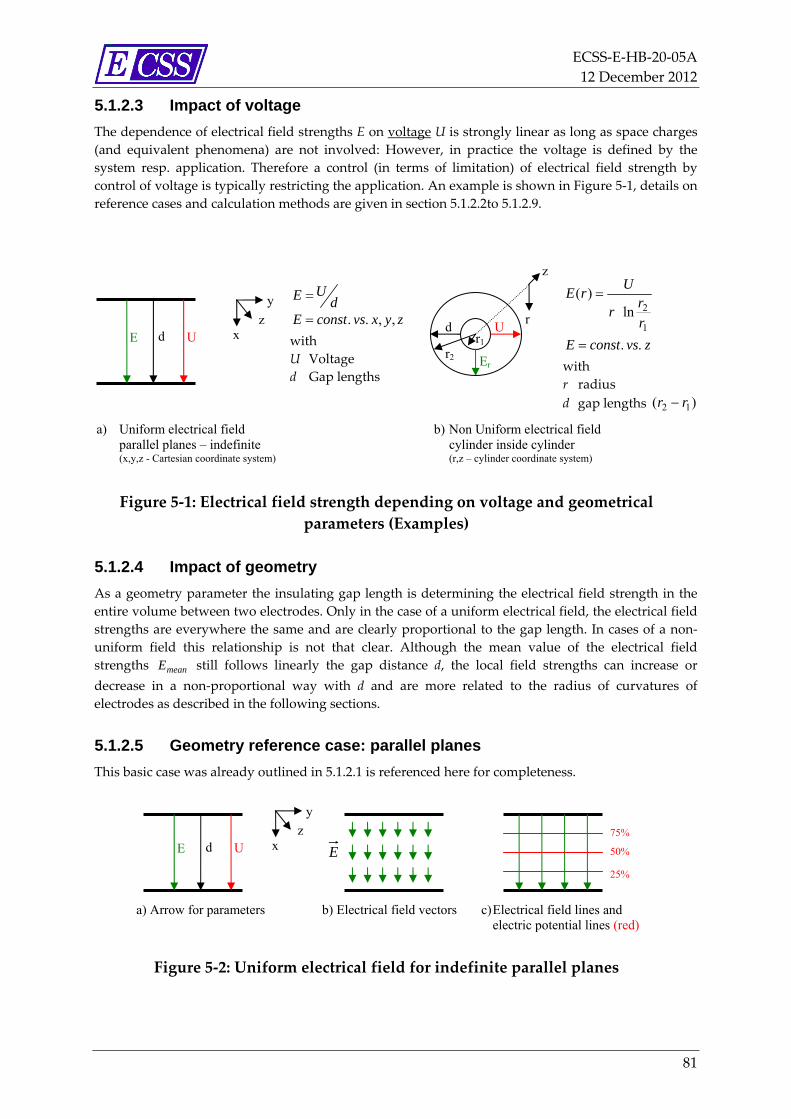
ECSS‐E‐HB‐20‐05A
12 December 2012
81
5.1.2.3 Impact of voltage
The dependence of electrical field strengths E on voltage U is strongly linear as long as space charges
(and equivalent phenomena) are not involved: However, in practice the voltage is defined by the
system resp. application. Therefore a control (in terms of limitation) of electrical field strength by
control of voltage is typically restricting the application. An example is shown in Figure 5‐1, details on
reference cases and calculation methods are given in section 5.1.2.2to 5.1.2.9.
Figure 5‐1: Electrical field strength depending on voltage and geometrical
parameters (Examples)
5.1.2.4 Impact of geometry
As a geometry parameter the insulating gap length is determining the electrical field strength in the
entire volume between two electrodes. Only in the case of a uniform electrical field, the electrical field
strengths are everywhere the same and are clearly proportional to the gap length. In cases of a non‐
uniform field this relationship is not that clear. Although the mean value of the electrical field
strengths meanE still follows linearly the gap distance d, the local field strengths can increase or
decrease in a non‐proportional way with d and are more related to the radius of curvatures of
electrodes as described in the following sections.
5.1.2.5 Geometry reference case: parallel planes
This basic case was already outlined in 5.1.2.1 is referenced here for completeness.
Figure 5‐2: Uniform electrical field for indefinite parallel planes
U E d
y
x z
E
a) Arrow for parameters b) Electrical field vectors c) Electrical field lines and electric potential lines (red)
50%
75%
25%
a) Uniform electrical field parallel planes – indefinite (x,y,z - Cartesian coordinate system)
U E d
dUE
zyxvsconstE ,,..with
U Voltage
d Gap lengths
y
x z
b) Non Uniform electrical field cylinder inside cylinder (r,z – cylinder coordinate system)
U d
r2 r1
Er
1
2ln)(
r
rr
UrE
zvsconstE ..
with
r radius
d gap lengths )( 12 rr
r
z
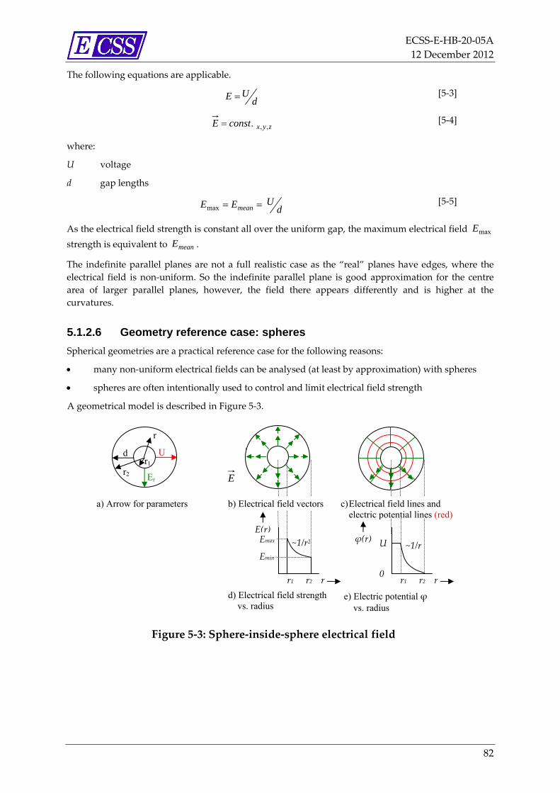
ECSS‐E‐HB‐20‐05A
12 December 2012
82
The following equations are applicable.
dUE [5‐3]
zyxconstE ,,. [5‐4]
where:
U voltage
d gap lengths
dUEE mean max [5‐5]
As the electrical field strength is constant all over the uniform gap, the maximum electrical field maxE
strength is equivalent to meanE .
The indefinite parallel planes are not a full realistic case as the “real” planes have edges, where the
electrical field is non‐uniform. So the indefinite parallel plane is good approximation for the centre
area of larger parallel planes, however, the field there appears differently and is higher at the
curvatures.
5.1.2.6 Geometry reference case: spheres
Spherical geometries are a practical reference case for the following reasons:
many non‐uniform electrical fields can be analysed (at least by approximation) with spheres
spheres are often intentionally used to control and limit electrical field strength
A geometrical model is described in Figure 5‐3.
Figure 5‐3: Sphere‐inside‐sphere electrical field
E
a) Arrow for parameters b) Electrical field vectors c) Electrical field lines and electric potential lines (red)
U d
r2 r1
Er
U
r
E(r)
rr1 r2
d) Electrical field strength vs. radius
ϕ(r)
r r1 r2
~1/r
e) Electric potential ϕ vs. radius
Emax
Emin
U
0
~1/r2

ECSS‐E‐HB‐20‐05A
12 December 2012
83
The following equations are applicable:
12
2 11)(
rrr
UrE 12 rr
Ud
UEmean
12
21
max
rr
r
UE
[5‐6] [5‐7] [5‐8]
where:
U: voltage,
r: radius (from centre),
1r radius of inner sphere,
2r radius of outer sphere
Conclusions for practical high voltage design with sphere‐inside‐sphere geometries are:
the max. electrical field strengths increases to high values
if the inner sphere is too small
if the ratio between inner outer sphere (radius) is too small
an optimum for the size of an insulation is reached, if the following condition is met:
12 2 rr [5‐9]
In case of a sphere in a free space the geometrical parameter 2r results in a simplified set of
equations:
12)( r
r
UrE
1max
r
UE
[5‐10] [5‐11]
Conclusions for practical high voltage design with sharp edges structures are:
select a minimum radius of a conductive high voltage structure to limit the maximum electrical
field strengths – following maxE definition with equation [5‐11] the resulting “law” is
max1 E
Ur
[5‐12]
this rule is valid as long as your counter‐electrode is still far away from the spherical structure
(means acc. to equation [5‐9] is 12 rr ).
for a first assessment equations [5‐8] and [5‐11] can be used of critical field strengths in any
design for sphere‐like structures.
Some examples for the selection of the proper radius are given in Table 5‐3.
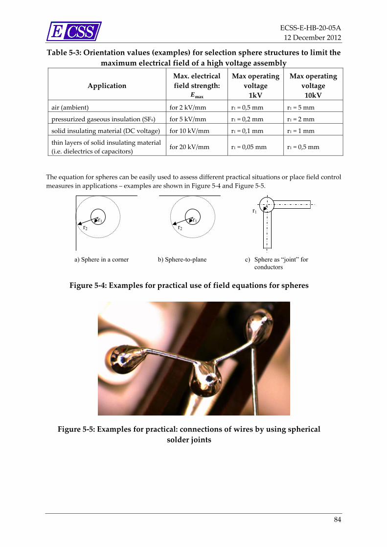
ECSS‐E‐HB‐20‐05A
12 December 2012
84
Table 5‐3: Orientation values (examples) for selection sphere structures to limit the
maximum electrical field of a high voltage assembly
Application
Max. electrical
field strength:
maxE
Max operating
voltage
1kV
Max operating
voltage
10kV
air (ambient) for 2 kV/mm r1 = 0,5 mm r1 = 5 mm
pressurized gaseous insulation (SF6) for 5 kV/mm r1 = 0,2 mm r1 = 2 mm
solid insulating material (DC voltage) for 10 kV/mm r1 = 0,1 mm r1 = 1 mm
thin layers of solid insulating material
(i.e. dielectrics of capacitors) for 20 kV/mm r1 = 0,05 mm r1 = 0,5 mm
The equation for spheres can be easily used to assess different practical situations or place field control
measures in applications – examples are shown in Figure 5‐4 and Figure 5‐5.
Figure 5‐4: Examples for practical use of field equations for spheres
Figure 5‐5: Examples for practical: connections of wires by using spherical
solder joints
a) Sphere in a corner
r2 r1
b) Sphere-to-plane
r2 r1
c) Sphere as “joint” for conductors
r1
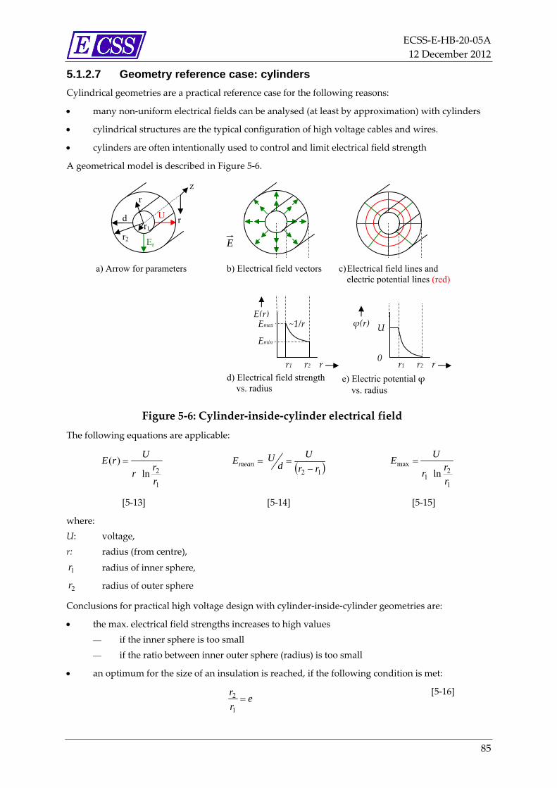
ECSS‐E‐HB‐20‐05A
12 December 2012
85
5.1.2.7 Geometry reference case: cylinders
Cylindrical geometries are a practical reference case for the following reasons:
many non‐uniform electrical fields can be analysed (at least by approximation) with cylinders
cylindrical structures are the typical configuration of high voltage cables and wires.
cylinders are often intentionally used to control and limit electrical field strength
A geometrical model is described in Figure 5‐6.
Figure 5‐6: Cylinder‐inside‐cylinder electrical field
The following equations are applicable:
1
2ln)(
r
rr
UrE 12 rr
Ud
UEmean
1
21
max
lnr
rr
UE
[5‐13] [5‐14] [5‐15]
where:
U: voltage,
r: radius (from centre),
1r radius of inner sphere,
2r radius of outer sphere
Conclusions for practical high voltage design with cylinder‐inside‐cylinder geometries are:
the max. electrical field strengths increases to high values
if the inner sphere is too small
if the ratio between inner outer sphere (radius) is too small
an optimum for the size of an insulation is reached, if the following condition is met:
er
r
1
2
[5‐16]
E
a) Arrow for parameters b) Electrical field vectors c) Electrical field lines and electric potential lines (red)
U d
r2 r1
Er
U
r
r
z
d) Electrical field strength vs. radius
e) Electric potential ϕ vs. radius
E(r)
rr1 r2
ϕ(r)
r r1 r2
Emax
Emin
U
0
~1/r
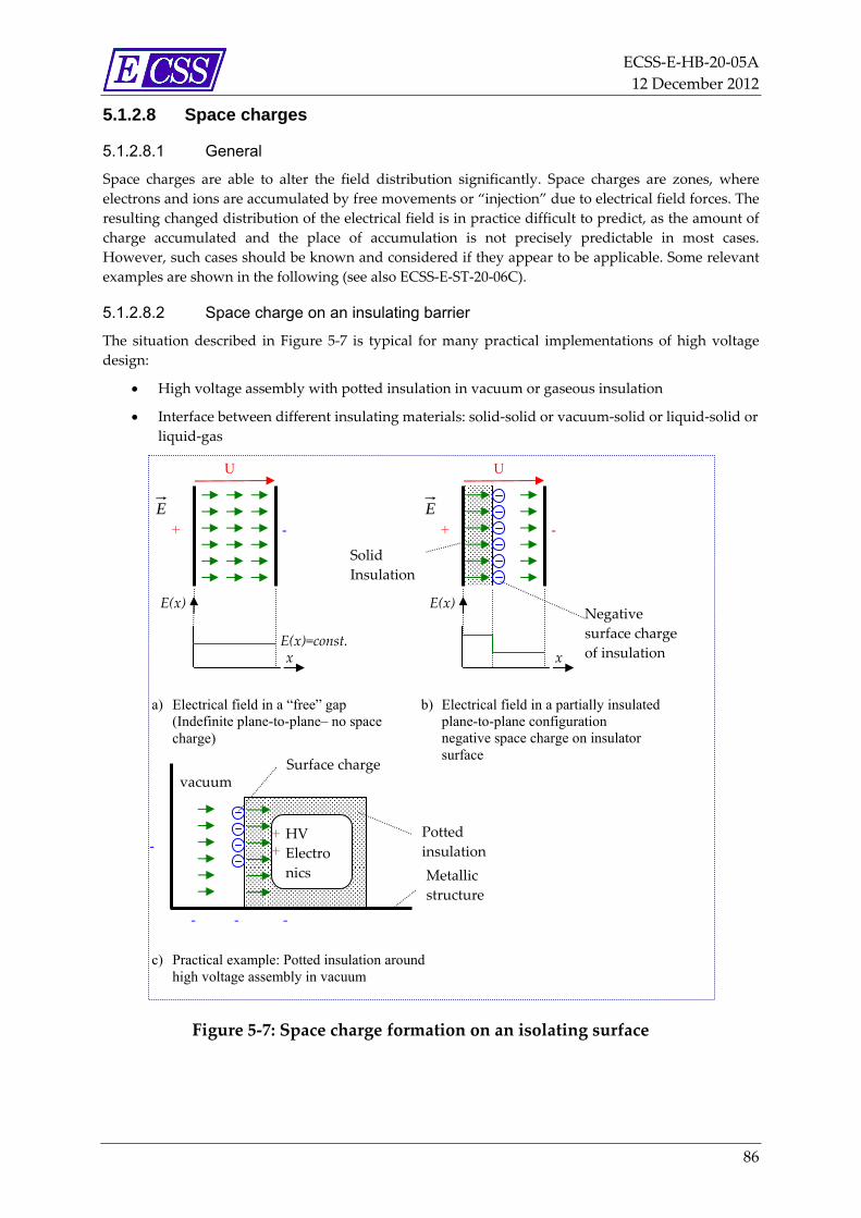
ECSS‐E‐HB‐20‐05A
12 December 2012
86
5.1.2.8 Space charges
5.1.2.8.1 General
Space charges are able to alter the field distribution significantly. Space charges are zones, where
electrons and ions are accumulated by free movements or “injection” due to electrical field forces. The
resulting changed distribution of the electrical field is in practice difficult to predict, as the amount of
charge accumulated and the place of accumulation is not precisely predictable in most cases.
However, such cases should be known and considered if they appear to be applicable. Some relevant
examples are shown in the following (see also ECSS‐E‐ST‐20‐06C).
5.1.2.8.2 Space charge on an insulating barrier
The situation described in Figure 5‐7 is typical for many practical implementations of high voltage
design:
High voltage assembly with potted insulation in vacuum or gaseous insulation
Interface between different insulating materials: solid‐solid or vacuum‐solid or liquid‐solid or
liquid‐gas
Figure 5‐7: Space charge formation on an isolating surface
E
a) Electrical field in a “free” gap (Indefinite plane-to-plane– no space charge)
U
+ -
E(x)
x E(x)=const.
E
b) Electrical field in a partially insulated plane-to-plane configuration negative space charge on insulator surface
U
+ -
E(x)
x
Solid
Insulation
Negative
surface charge
of insulation
c) Practical example: Potted insulation around high voltage assembly in vacuum
HV
Electro
nics
Potted
insulation
Metallic
structure
+
-
-
Surface chargevacuum
- -
+
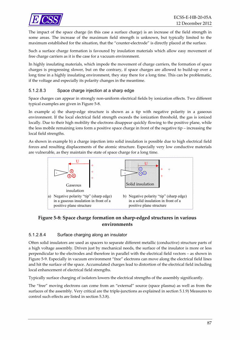
ECSS‐E‐HB‐20‐05A
12 December 2012
87
The impact of the space charge (in this case a surface charge) is an increase of the field strength in
some areas. The increase of the maximum field strength is unknown, but typically limited to the
maximum established for the situation, that the “counter‐electrode” is directly placed at the surface.
Such a surface charge formation is favoured by insulation materials which allow easy movement of
free charge carriers as it is the case for a vacuum environment.
In highly insulating materials, which impede the movement of charge carriers, the formation of space
charges is progressing slower, but on the contrary, if space charges are allowed to build‐up over a
long time in a highly insulating environment, they stay there for a long time. This can be problematic,
if the voltage and especially its polarity changes in the meantime.
5.1.2.8.3 Space charge injection at a sharp edge
Space charges can appear in strongly non‐uniform electrical fields by ionization effects. Two different
typical examples are given in Figure 5‐8.
In example a) the sharp‐edge structure is shown as a tip with negative polarity in a gaseous
environment. If the local electrical field strength exceeds the ionization threshold, the gas is ionized
locally. Due to their high mobility the electrons disappear quickly flowing to the positive plane, while
the less mobile remaining ions form a positive space charge in front of the negative tip – increasing the
local field strengths.
As shown in example b) a charge injection into solid insulation is possible due to high electrical field
forces and resulting displacements of the atomic structure. Especially very low conductive materials
are vulnerable, as they maintain the state of space charge for a long time.
Figure 5‐8: Space charge formation on sharp‐edged structures in various
environments
5.1.2.8.4 Surface charging along an insulator
Often solid insulators are used as spacers to separate different metallic (conductive) structure parts of
a high voltage assembly. Driven just by mechanical needs, the surface of the insulator is more or less
perpendicular to the electrodes and therefore in parallel with the electrical field vectors – as shown in
Figure 5‐9. Especially in vacuum environment “free” electrons can move along the electrical field lines
and hit the surface of the space. Accumulated charges lead to distortion of the electrical field including
local enhancement of electrical field strengths.
Typically surface charging of isolators lowers the electrical strengths of the assembly significantly.
The “free” moving electrons can come from an “external” source (space plasma) as well as from the
surfaces of the assembly. Very critical are the triple‐junctions as explained in section 5.1.9) Measures to
control such effects are listed in section 5.3.8).
-
Gaseous
insulation
+
+
+
Solid insulation
+
U U
a) Negative polarity “tip” (sharp edge) in a gaseous insulation in front of a positive plane structure
b) Negative polarity “tip” (sharp edge) in a solid insulation in front of a positive plane structure
- +
+
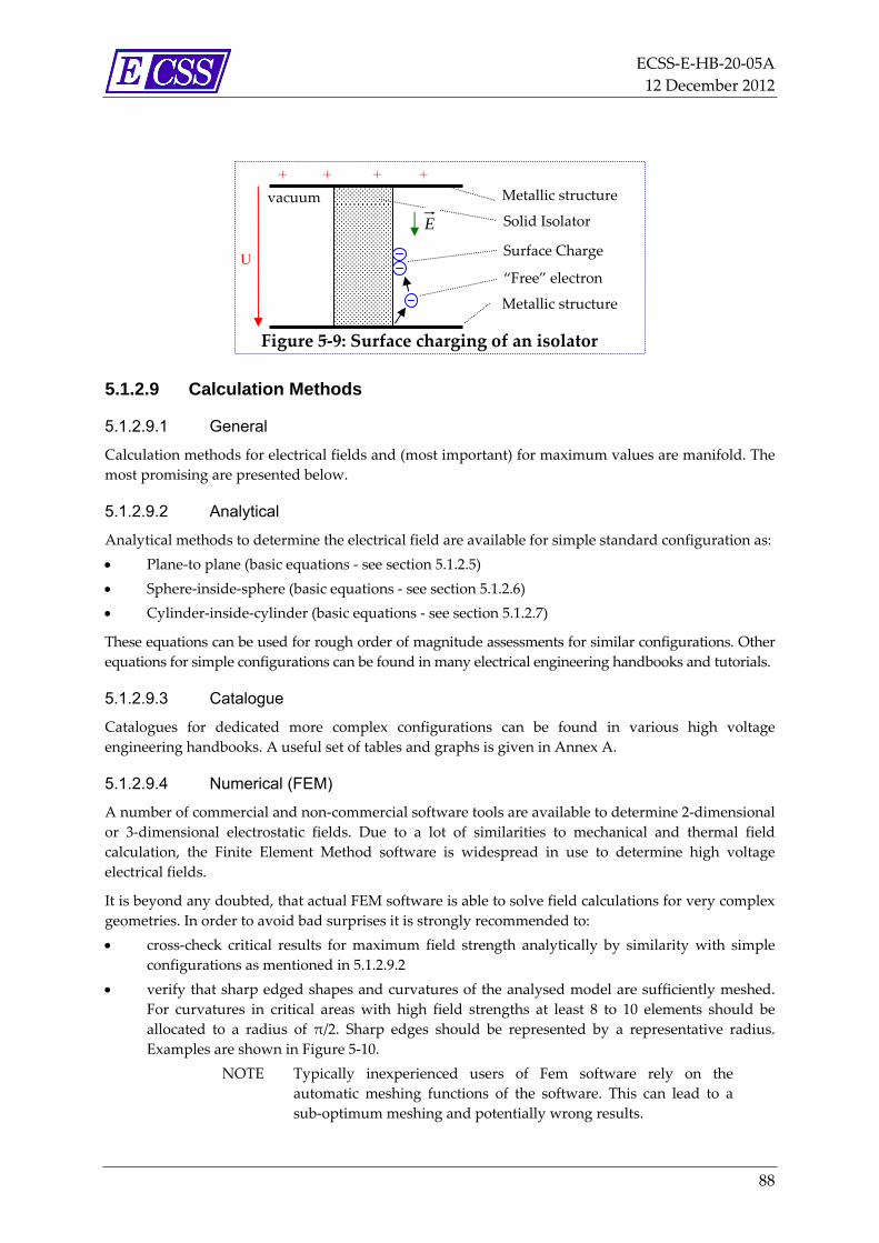
ECSS‐E‐HB‐20‐05A
12 December 2012
88
Figure 5‐9: Surface charging of an isolator
5.1.2.9 Calculation Methods
5.1.2.9.1 General
Calculation methods for electrical fields and (most important) for maximum values are manifold. The
most promising are presented below.
5.1.2.9.2 Analytical
Analytical methods to determine the electrical field are available for simple standard configuration as:
Plane‐to plane (basic equations ‐ see section 5.1.2.5)
Sphere‐inside‐sphere (basic equations ‐ see section 5.1.2.6)
Cylinder‐inside‐cylinder (basic equations ‐ see section 5.1.2.7)
These equations can be used for rough order of magnitude assessments for similar configurations. Other
equations for simple configurations can be found in many electrical engineering handbooks and tutorials.
5.1.2.9.3 Catalogue
Catalogues for dedicated more complex configurations can be found in various high voltage
engineering handbooks. A useful set of tables and graphs is given in Annex A.
5.1.2.9.4 Numerical (FEM)
A number of commercial and non‐commercial software tools are available to determine 2‐dimensional
or 3‐dimensional electrostatic fields. Due to a lot of similarities to mechanical and thermal field
calculation, the Finite Element Method software is widespread in use to determine high voltage
electrical fields.
It is beyond any doubted, that actual FEM software is able to solve field calculations for very complex
geometries. In order to avoid bad surprises it is strongly recommended to:
cross‐check critical results for maximum field strength analytically by similarity with simple
configurations as mentioned in 5.1.2.9.2
verify that sharp edged shapes and curvatures of the analysed model are sufficiently meshed.
For curvatures in critical areas with high field strengths at least 8 to 10 elements should be
allocated to a radius of π/2. Sharp edges should be represented by a representative radius.
Examples are shown in Figure 5‐10.
NOTE Typically inexperienced users of Fem software rely on the
automatic meshing functions of the software. This can lead to a
sub‐optimum meshing and potentially wrong results.
Solid Isolator
-
vacuum
- - -
+ + + +
Metallic structure
Metallic structure
Surface Charge
“Free” electron
U
E
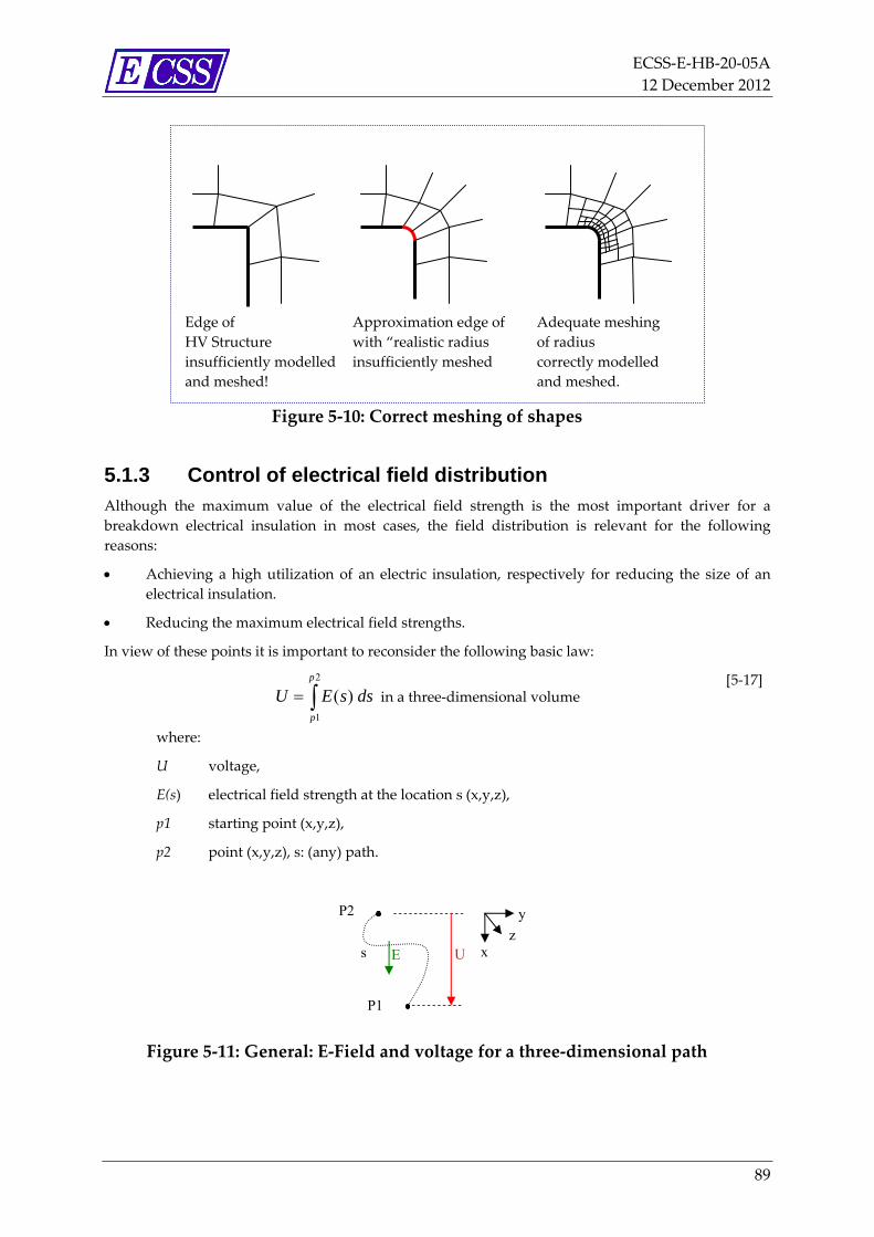
ECSS‐E‐HB‐20‐05A
12 December 2012
89
Figure 5‐10: Correct meshing of shapes
5.1.3 Control of electrical field distribution Although the maximum value of the electrical field strength is the most important driver for a
breakdown electrical insulation in most cases, the field distribution is relevant for the following
reasons:
Achieving a high utilization of an electric insulation, respectively for reducing the size of an
electrical insulation.
Reducing the maximum electrical field strengths.
In view of these points it is important to reconsider the following basic law:
where:
U voltage,
E(s) electrical field strength at the location s (x,y,z),
p1 starting point (x,y,z),
p2 point (x,y,z), s: (any) path.
Figure 5‐11: General: E‐Field and voltage for a three‐dimensional path
2
1
)(p
p
dssEU in a three‐dimensional volume [5‐17]
U E
P1
y
x z
s
P2
Edge of
HV Structure
insufficiently modelled
and meshed!
Approximation edge of
with “realistic radius
insufficiently meshed
Adequate meshing
of radius
correctly modelled
and meshed.
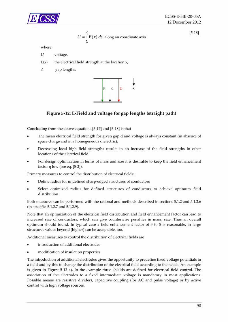
ECSS‐E‐HB‐20‐05A
12 December 2012
90
where:
U voltage,
E(x) the electrical field strength at the location x,
d gap lengths.
Figure 5‐12: E‐Field and voltage for gap lengths (straight path)
Concluding from the above equations [5‐17] and [5‐18] is that
The mean electrical field strength for given gap d and voltage is always constant (in absence of
space charge and in a homogeneous dielectric).
Decreasing local high field strengths results in an increase of the field strengths in other
locations of the electrical field.
For design optimization in terms of mass and size it is desirable to keep the field enhancement
factor η low (see eq. [5‐2]).
Primary measures to control the distribution of electrical fields:
Define radius for undefined sharp‐edged structures of conductors
Select optimized radius for defined structures of conductors to achieve optimum field
distribution
Both measures can be performed with the rational and methods described in sections 5.1.2 and 5.1.2.6
(in specific: 5.1.2.7 and 5.1.2.9).
Note that an optimization of the electrical field distribution and field enhancement factor can lead to
increased size of conductors, which can give counterwise penalties in mass, size. Thus an overall
optimum should found. In typical case a field enhancement factor of 3 to 5 is reasonable, in large
structures values beyond (higher) can be acceptable, too.
Additional measures to control the distribution of electrical fields are
introduction of additional electrodes
modification of insulation properties
The introduction of additional electrodes gives the opportunity to predefine fixed voltage potentials in
a field and by this to change the distribution of the electrical field according to the needs. An example
is given in Figure 5‐13 a). In the example three shields are defined for electrical field control. The
association of the electrodes to a fixed intermediate voltage is mandatory in most applications.
Possible means are resistive dividers, capacitive coupling (for AC and pulse voltage) or by active
control with high voltage sources.
d
dsxEU0
)( along an coordinate axis [5‐18]
x U E d
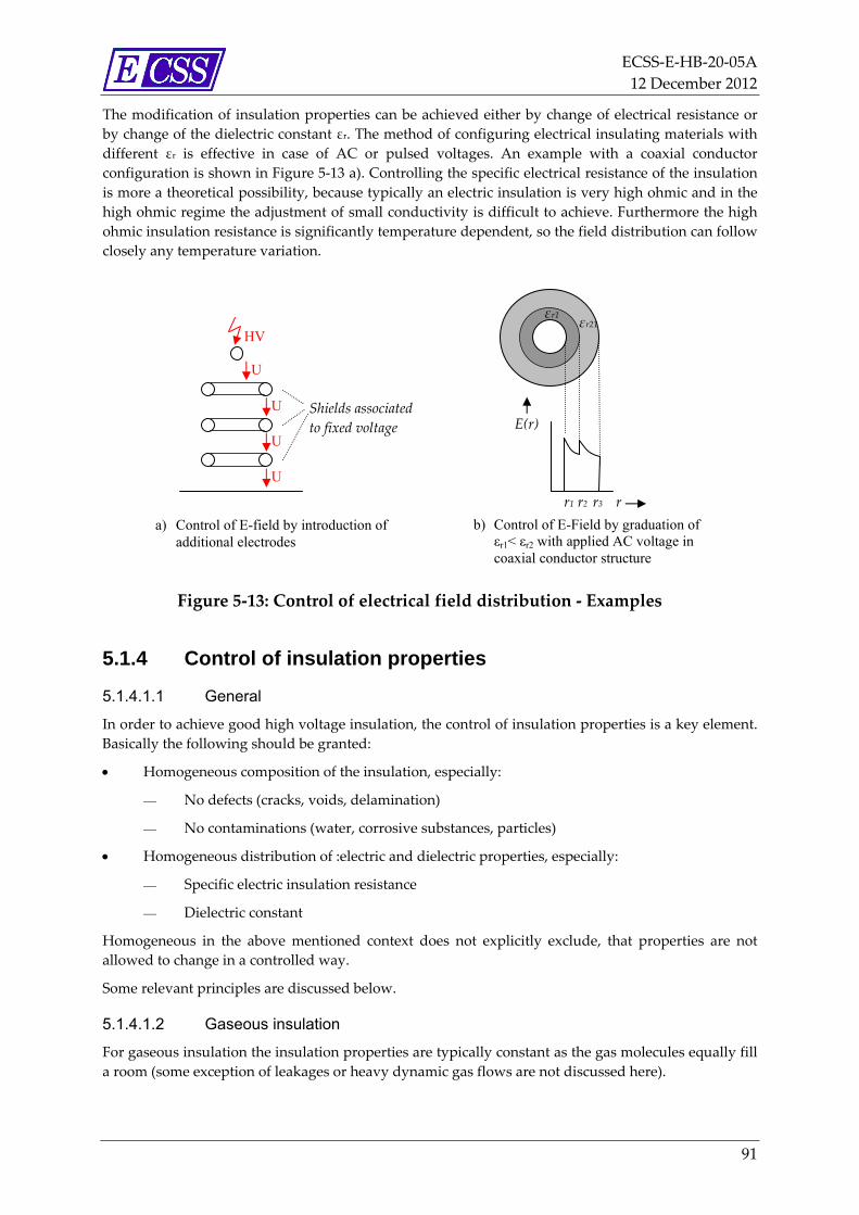
ECSS‐E‐HB‐20‐05A
12 December 2012
91
The modification of insulation properties can be achieved either by change of electrical resistance or
by change of the dielectric constant εr. The method of configuring electrical insulating materials with
different εr is effective in case of AC or pulsed voltages. An example with a coaxial conductor
configuration is shown in Figure 5‐13 a). Controlling the specific electrical resistance of the insulation
is more a theoretical possibility, because typically an electric insulation is very high ohmic and in the
high ohmic regime the adjustment of small conductivity is difficult to achieve. Furthermore the high
ohmic insulation resistance is significantly temperature dependent, so the field distribution can follow
closely any temperature variation.
Figure 5‐13: Control of electrical field distribution ‐ Examples
5.1.4 Control of insulation properties
5.1.4.1.1 General
In order to achieve good high voltage insulation, the control of insulation properties is a key element.
Basically the following should be granted:
Homogeneous composition of the insulation, especially:
No defects (cracks, voids, delamination)
No contaminations (water, corrosive substances, particles)
Homogeneous distribution of :electric and dielectric properties, especially:
Specific electric insulation resistance
Dielectric constant
Homogeneous in the above mentioned context does not explicitly exclude, that properties are not
allowed to change in a controlled way.
Some relevant principles are discussed below.
5.1.4.1.2 Gaseous insulation
For gaseous insulation the insulation properties are typically constant as the gas molecules equally fill
a room (some exception of leakages or heavy dynamic gas flows are not discussed here).
a) Control of E-field by introduction of additional electrodes
E(r)
r r1 r3
b) Control of E-Field by graduation of εr1< εr2 with applied AC voltage in coaxial conductor structure
r2
εr21εr1
U
U
U
Shields associated
to fixed voltage
U
HV

ECSS‐E‐HB‐20‐05A
12 December 2012
92
5.1.4.1.3 Vacuum insulation
For vacuum insulation there is no issue regarding the insulation properties itself, however, surface
and residual gases play an important role for breakdown. For details see section 5.2.5 and section
4.3.4.
5.1.4.1.4 Liquid insulation
For liquid insulation the following most important effects should be controlled:
Fibres
In order to achieve high electric strengths fibre and similar contaminations should be either
strictly avoided or its impact in building fibre bridges should be suppressed. In most of the
cases the introduction of barriers is an efficient measure (see Figure 5‐14).
Figure 5‐14: Avoiding fibre bridging effect in liquid insulation
Gas bubbles
Formation of gas bubbles should be avoided. Gas bubbles can be the result of partial discharge
or of transitioning the threshold of vapour pressure. So as countermeasures:
partial discharges should be avoided (see section 5.1.7 Control of corona effects)
the gas should be always under sufficient pressurization
if the bubble is small enough, the voltage across it is below the Paschen minimum, thus
eliminating the problem of discharges
solved gases should be removed under low pressure
filling under absence of gases (i.e. under vacuum, if appropriate).
5.1.4.1.5 Solid insulation
For solid insulation the following most important effects should be controlled:
Avoiding cracks and delamination
Cracks and delamination in an area with high field stress is a starting point for breakdown of a
solid insulation. Suitable countermeasures are:
Selection of a suitable manufacturing process
Favourable manufacturing processes are:
o moulding/potting,
o sintering
o extruding
Additional advantage can be achieved with processes allowing
o performance of essential steps of processing under vacuum to avoid inclusions of
air (bubbles), respectively of air bubble size reduction after repressurization
E
a) Liquid filled gap starting built-up offibre bridges
b) Preventing of fibre bridges by barriers, here: insulation foils
ECSS‐E‐HB‐20‐05A
12 December 2012
93
o gapless contact with electrodes and conductors.
Selection of suitable materials
Favourable solid insulation materials should be compatible with the above mentioned
favourable manufacturing processes. Important roles for high voltage design for space
applications are playing the following materials:
o Polymeric materials, most important epoxy resins, polyurethane resins, silicon
resins, flour ethylene polymers (PTFE (Teflon ™), FEP), polyimide (Kapton ™,
Vespel ™)
o Ceramic materials
o Mica
Avoiding high electrical field stresses along interfaces
In many high voltage insulation applications it is unavoidable to have discontinuities in
structure of the insulation. Reasons for such discontinuities can be:
Composites of different materials for optimum properties of insulation (i.e. glass‐fibre
reinforced material for thermo‐mechanical strength improvement)
Sequential manufacturing steps (i.e. potting of an assembly in a series of moulding,
potting, hardening steps)
Interfacing of different materials with glue (etc.)
Filling gaps between materials with glue (etc.)
Wrapping or shrinking materials onto other materials
The consequences for design of high voltage insulations under such circumstances are the
following:
Typically the breakdown strength is significantly lower, if the vector of the electrical field
strengths is in the direction of the interface (between two insulations) – see Figure 5‐15 a.
Therefore the vector of the electrical field should be preferably perpendicular to the
interface of the materials – see Figure 5‐15 b.
In case that a perpendicular orientation is not possible, an interleaved interface can be
advantageous– see Figure 5‐15 c. An interleaved interface can be more easily realized
with potting materials, and is typically difficult to achieve with machined parts on both
sides of the interface as gaps cannot be avoided.
Otherwise the electrical field strengths applied should be significantly lowered compared
to those of the “pure” materials.
If an interface area is situated close to ground or to a high voltage electrode the field
stress can be locally reduced by introduction of shield electrodes – these measures are
identical to those proposed to control triple‐junction areas and are explained there (see
section 5.1.9).
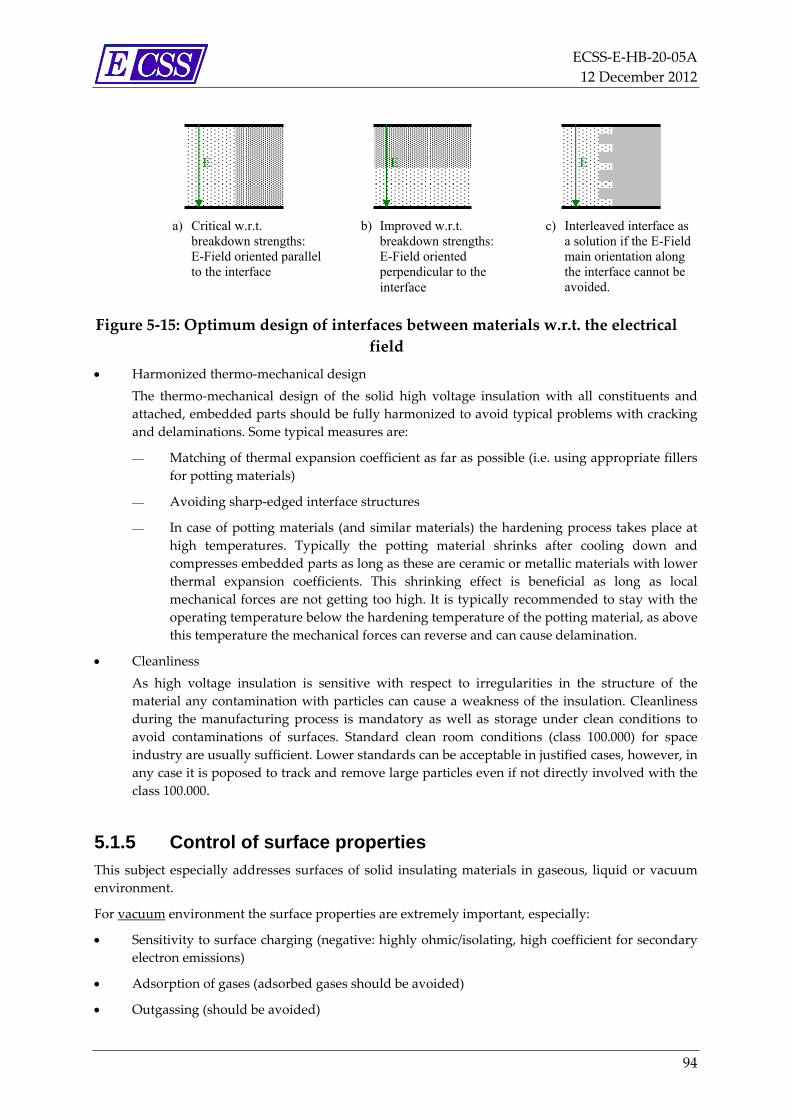
ECSS‐E‐HB‐20‐05A
12 December 2012
94
Figure 5‐15: Optimum design of interfaces between materials w.r.t. the electrical
field
Harmonized thermo‐mechanical design
The thermo‐mechanical design of the solid high voltage insulation with all constituents and
attached, embedded parts should be fully harmonized to avoid typical problems with cracking
and delaminations. Some typical measures are:
Matching of thermal expansion coefficient as far as possible (i.e. using appropriate fillers
for potting materials)
Avoiding sharp‐edged interface structures
In case of potting materials (and similar materials) the hardening process takes place at
high temperatures. Typically the potting material shrinks after cooling down and
compresses embedded parts as long as these are ceramic or metallic materials with lower
thermal expansion coefficients. This shrinking effect is beneficial as long as local
mechanical forces are not getting too high. It is typically recommended to stay with the
operating temperature below the hardening temperature of the potting material, as above
this temperature the mechanical forces can reverse and can cause delamination.
Cleanliness
As high voltage insulation is sensitive with respect to irregularities in the structure of the
material any contamination with particles can cause a weakness of the insulation. Cleanliness
during the manufacturing process is mandatory as well as storage under clean conditions to
avoid contaminations of surfaces. Standard clean room conditions (class 100.000) for space
industry are usually sufficient. Lower standards can be acceptable in justified cases, however, in
any case it is poposed to track and remove large particles even if not directly involved with the
class 100.000.
5.1.5 Control of surface properties This subject especially addresses surfaces of solid insulating materials in gaseous, liquid or vacuum
environment.
For vacuum environment the surface properties are extremely important, especially:
Sensitivity to surface charging (negative: highly ohmic/isolating, high coefficient for secondary
electron emissions)
Adsorption of gases (adsorbed gases should be avoided)
Outgassing (should be avoided)
E
a) Critical w.r.t. breakdown strengths: E-Field oriented parallel to the interface
E
b) Improved w.r.t. breakdown strengths: E-Field oriented perpendicular to the interface
E
c) Interleaved interface as a solution if the E-Field main orientation along the interface cannot be avoided.
ECSS‐E‐HB‐20‐05A
12 December 2012
95
Hydroscopic properties (should be avoided)
Roughness (rough surface appears to be advantageous over flat surface)
Shape (should prevent surface charging, see section 5.3.8)
Particle contamination (should be avoided).
The relevant aspects are explained in section 5.2.5.
For gaseous environment the following surface properties are important:
Hydroscopic properties (should be avoided)
Wetting by water (should be avoided)
Shape (should increase the lengths of a conductive path, see section 5.3.8).
For liquid environment the following surface properties are important:
Hydroscopic properties (should be avoided)
Shape (should increase the lengths of a conductive path, see section 5.3.8).
Possible methods to control surface properties in general:
Machining
provides the basic shape and can control the surface roughness.
Polishing (mechanical)
minimizes surface roughness
Thermal treatment
is useful for drying and quick removing of adsorbed gases under vacuum
Plasma treatment
removes surface layers and controls surface roughness
Coating
can alter the surface properties of the substrate material
Examples: silicon coating to increase hydrophobic properties or conductive (high ohmic)
coating to reduce surface charging effects.
Additives
to control surface conductivity
Cleaning with fluids
to remove surface layers and humidity
ECSS‐E‐HB‐20‐05A
12 December 2012
96
5.1.6 Control of partial discharges Partial discharges should be kept under a maximum level to avoid continued erosion of the insulation
causing a long‐term breakdown. The critical levels depend on the type of material and typically range
from 1 pC to 20 pC, for some partial discharge resistant materials (like mica) levels of a few 100 pC can
be acceptable, too (see more details in section 5.3.2).
The measures to control the level of partial discharges are depending on the type of insulation.
In gaseous insulation the important factors are
Electrical field strengths
Limiting the (local) maximum electrical field strengths to a value below the breakdown field
strengths is in most cases the only measure to avoid partial discharges in gaseous insulations.
These values are in accordance with section 4.3.2.2 and cannot be changed only by changing the
material (gas). A very useful strategy in many applications is to mix or replace “gases” by (or
with) SF6‐gas.
Particles
Loose particles can be a problem in gas insulations with very high breakdown field strengths,
which can by high compressed (few atmospheres) insulating gases like SF6‐gas. Particle
movement can appear under high electrical field forces causing partial discharges – so called
“particle bouncing”. Cleanliness during manufacturing and integration of such insulation is a
key factor to avoid problem to be caused by particles.
In liquid insulation the important factors are
Electrical field strengths
Limiting the (local) maximum electrical field strengths to a value below the breakdown field
strengths is in most cases the only measure to avoid partial discharges in liquid insulations. As
the on‐set threshold for partial discharges is typically very much depending on contaminations
the avoidance of particles and solved gas / gas bubbles is important.
Particles
Particles need to be consequently avoided by filtering of the liquid (before filling), cleaning of
the surfaces being in contact with the liquid, using particle/abrasion free surfaces (coating if
necessary).
Gas bubbles (Solved gases).
First, gas content in liquids should be avoided, if possible. Suitable measure can be degassing
under low pressure and vacuum. Contact to gaseous environment (ambient air, etc) should be
avoided after degassing (if possible by design and handling).
If gas content is unavoidable, the liquid should be kept under sufficient pressure to avoid
formation of gas bubbles.
In solid insulation the important factors are
Electrical field strengths
Limiting the (local) maximum electrical field strengths is useful in the way of achieving a most
uniform electrical field distribution, respectively a homogeneous field. With a few exceptions
(short lifetime equipments, partial discharge resistant materials, etc.) partial discharge should
not appear, which means in practice partial discharge levels below a few to few ten
Picocoulombs. The maximum operating field strengths should be selected in respect of this.

ECSS‐E‐HB‐20‐05A
12 December 2012
97
Gas filled‐gaps, delamination, gas bubbles, voids
Irregularities inside the solid insulation and at the interface between insulation and the
conductors/electrodes should be avoided, which means
Avoid gas filled volumes (enclosed gas bubbles, gaps, etc.)
Avoid enclosure of particles, especially metallic particles (abrasions) and inclusions with
different dielectric properties than the original materials
Avoid structural changes of the material
NOTE The strategy of avoiding enclosure of particles and structural
changes does not ignore the fact, that some there is a suitable
compound material (filled epoxy resin, mica compounds etc.) with
a natural “content” of structural discontinuities, which can still
achieve good dielectric strengths when exposed to a high level of
severe partial discharges
In vacuum insulation partial discharges do not exist according to the definitions given in section 4.3.3.
However, there are so called micro‐discharges and pre‐breakdown currents, which can be interpreted
by a detector as partial discharges.
In general it should be noted, that AC applications are representing the most critical case w.r.t. partial
discharges and its (long‐term) erosive effects. In DC and in unipolar pulse application partial
discharges appear less frequently, so the impact on ageing is less severe in most cases, but can never
be neglected.
5.1.7 Control of corona effects
The expression “corona” is often used with different meanings. From the origin it means a light
emitting discharge around a conductor. Such a phenomenon can be related to
(Outer) partial discharges in a gaseous environment
As outlined in sections 5.1.6 this effect can be avoided by
Geometry: increasing distance and large radius of curvature of electrodes in order to
reduce the maximum field strengths
Mixture or substitution of the original gas with a stronger gas mixture with higher
breakdown field strength
(Inner) partial discharges in gas‐filled gaps and voids of solid or liquid insulations
Measures are outlined in section 5.1.6
Paschen breakdown
Measures are outlined in section 5.1.8
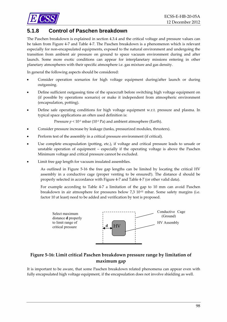
ECSS‐E‐HB‐20‐05A
12 December 2012
98
5.1.8 Control of Paschen breakdown The Paschen breakdown is explained in section 4.3.4 and the critical voltage and pressure values can
be taken from Figure 4‐7 and Table 4‐7. The Paschen breakdown is a phenomenon which is relevant
especially for non‐encapsulated equipments, exposed to the natural environment and undergoing the
transition from ambient air pressure on ground to space vacuum environment during and after
launch. Some more exotic conditions can appear for interplanetary missions entering in other
planetary atmospheres with their specific atmosphere i.e. gas mixture and gas density.
In general the following aspects should be considered:
Consider operation scenarios for high voltage equipment during/after launch or during
outgassing.
Define sufficient outgassing time of the spacecraft before switching high voltage equipment on
(if possible by operations scenario) or make it independent from atmospheric environment
(encapsulation, potting).
Define safe operating conditions for high voltage equipment w.r.t. pressure and plasma. In
typical space applications an often used definition is:
Pressure p < 10‐5 mbar (10‐3 Pa) and ambient atmosphere (Earth).
Consider pressure increase by leakage (tanks, pressurized modules, thrusters).
Perform test of the assembly in a critical pressure environment (if critical).
Use complete encapsulation (potting, etc.), if voltage and critical pressure leads to unsafe or
unstable operation of equipment – especially if the operating voltage is above the Paschen
Minimum voltage and critical pressure cannot be excluded.
Limit free gap length for vacuum insulated assemblies.
As outlined in Figure 5‐16 the free gap lengths can be limited by locating the critical HV
assembly in a conductive cage (proper venting to be ensured!). The distance d should be
properly selected in accordance with Figure 4‐7 and Table 4‐7 (or other valid data).
For example according to Table 4‐7 a limitation of the gap to 10 mm can avoid Paschen
breakdown in air atmosphere for pressures below 7,3 10‐02 mbar. Some safety margins (i.e.
factor 10 at least) need to be added and verification by test is proposed.
Figure 5‐16: Limit critical Paschen breakdown pressure range by limitation of
maximum gap
It is important to be aware, that some Paschen breakdown related phenomena can appear even with
fully encapsulated high voltage equipment, if the encapsulation does not involve shielding as well.
Conductive Cage(Ground)
HV
Select maximum distance d properly to limit range of critical pressure d
HV Assembly
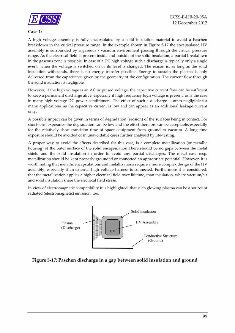
ECSS‐E‐HB‐20‐05A
12 December 2012
99
Case 1:
A high voltage assembly is fully encapsulated by a solid insulation material to avoid a Paschen
breakdown in the critical pressure range. In the example shown in Figure 5‐17 the encapsulated HV
assembly is surrounded by a gaseous / vacuum environment passing through the critical pressure
range. As the electrical field is present inside and outside of the solid insulation, a partial breakdown
in the gaseous zone is possible. In case of a DC high voltage such a discharge is typically only a single
event, when the voltage is switched on or its level is changed. The reason is: as long as the solid
insulation withstands, there is no energy transfer possible. Energy to sustain the plasma is only
delivered from the capacitance given by the geometry of the configuration. The current flow through
the solid insulation is negligible.
However, if the high voltage is an AC or pulsed voltage, the capacitive current flow can be sufficient
to keep a permanent discharge alive, especially if high frequency high voltage is present, as is the case
in many high voltage DC power conditioners. The effect of such a discharge is often negligible for
many applications, as the capacitive current is low and can appear as an additional leakage current
only.
A possible impact can be given in terms of degradation (erosion) of the surfaces being in contact. For
short‐term exposures the degradation can be low and the effect therefore can be acceptable, especially
for the relatively short transition time of space equipment from ground to vacuum. A long time
exposure should be avoided or in unavoidable cases further analysed by life‐testing.
A proper way to avoid the effects described for this case, is a complete metallization (or metallic
housing) of the outer surface of the solid encapsulation There should be no gaps between the metal
shield and the solid insulation in order to avoid any partial discharges. The metal case resp.
metallization should be kept properly grounded or connected an appropriate potential. However, it is
worth noting that metallic encapsulations and metallizations require a more complex design of the HV
assembly, especially if an external high voltage harness is connected. Furthermore it is considered,
that the metallization applies a higher electrical field over lifetime, than insulation, where vacuum/air
and solid insulation share the electrical field stress.
In view of electromagnetic compatibility it is highlighted, that such glowing plasma can be a source of
radiated (electromagnetic) emission, too.
Figure 5‐17: Paschen discharge in a gap between solid insulation and ground
Conductive Structure (Ground)
HV
Solid insulation
HV Assembly Plasma (Discharge)

ECSS‐E‐HB‐20‐05A
12 December 2012
100
Case 2:
The second problematic situation is related to the above described Case 1. Figure 5‐18 shows the
already described situation of plasma generated outside of a HV assembly which is encapsulate by a
solid insulation. In the critical pressure range plasma is generated and well supplied by an AC HV
source. A low voltage assembly with unprotected conductors is exposed to the plasma. As the plasma
provides a conductive path it can trigger a breakdown between the conductors (resulting in a short
circuit) even if the voltage is low.
Figure 5‐18: Triggered Paschen discharge in a gap between solid insulation and
ground
Therefore it is quite essential, that low voltage assemblies exposed to high voltage fields should be
properly encapsulated or coated with insulation material and/or shielded from the HV field (metallic
potential controlled shield.)
5.1.9 Control of triple junction effects The region of high voltage insulation, where three materials are joined together, is called the “triple
junction” region. This critical region is typically formed by the interface between:
Solid insulator – gaseous insulation – metal (conductor)
Solid insulator ‐ vacuum – metal (conductor)
Solid insulator – liquid insulation – metal (conductor)
An example is shown in Figure 5‐19.
Figure 5‐19: Critical triple‐junction point/area in an interface between solid ‐
gaseous/liquid/vacuum insulation ‐ metal conductor
Triple junction area
VacuumLiquid Gas
Isolator Solid
Conductive Cage(Ground)
HV
Solid insulation
HV Assembly
Plasma (Discharge)
Low voltage conductors
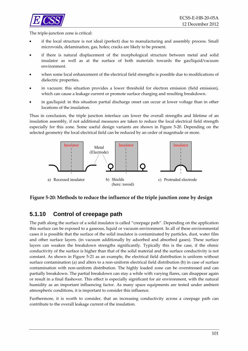
ECSS‐E‐HB‐20‐05A
12 December 2012
101
The triple‐junction zone is critical:
if the local structure is not ideal (perfect) due to manufacturing and assembly process. Small
microvoids, delamination, gas, holes; cracks are likely to be present.
if there is natural displacement of the morphological structure between metal and solid
insulator as well as at the surface of both materials towards the gas/liquid/vacuum
environment.
when some local enhancement of the electrical field strengths is possible due to modifications of
dielectric properties.
in vacuum: this situation provides a lower threshold for electron emission (field emission),
which can cause a leakage current or promote surface charging and resulting breakdown.
in gas/liquid: in this situation partial discharge onset can occur at lower voltage than in other
locations of the insulation.
Thus in conclusion, the triple junction interface can lower the overall strengths and lifetime of an
insulation assembly, if not additional measures are taken to reduce the local electrical field strength
especially for this zone. Some useful design variants are shown in Figure 5‐20. Depending on the
selected geometry the local electrical field can be reduced by an order of magnitude or more.
Figure 5‐20: Methods to reduce the influence of the triple junction zone by design
5.1.10 Control of creepage path
The path along the surface of a solid insulator is called “creepage path”. Depending on the application
this surface can be exposed to a gaseous, liquid or vacuum environment. In all of these environmental
cases it is possible that the surface of the solid insulator is contaminated by particles, dust, water film
and other surface layers. (in vacuum additionally by adsorbed and absorbed gases). These surface
layers can weaken the breakdown strengths significantly. Typically this is the case, if the ohmic
conductivity of the surface is higher than that of the solid material and the surface conductivity is not
constant. As shown in Figure 5‐21 as an example, the electrical field distribution is uniform without
surface contamination (a) and alters to a non‐uniform electrical field distribution (b) in case of surface
contamination with non‐uniform distribution. The highly loaded zone can be overstressed and can
partially breakdown. The partial breakdown can stay a while with varying flares, can disappear again
or result in a final flashover. This effect is especially significant for air environment, with the natural
humidity as an important influencing factor. As many space equipments are tested under ambient
atmospheric conditions, it is important to consider this influence.
Furthermore, it is worth to consider, that an increasing conductivity across a creepage path can
contribute to the overall leakage current of the insulation.
a) Recessed insulator b) Shields (here: toroid)
c) Protruded electrode
Insulator Insulator Insulator Metal (Electrode)
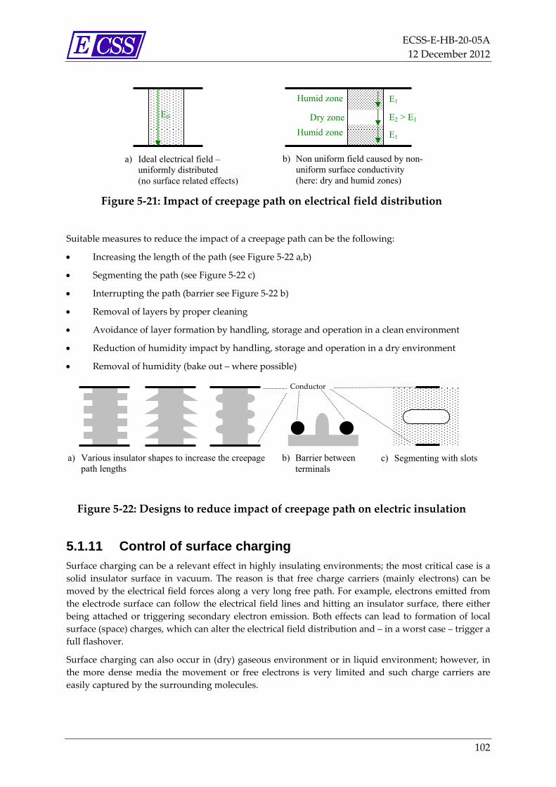
ECSS‐E‐HB‐20‐05A
12 December 2012
102
Figure 5‐21: Impact of creepage path on electrical field distribution
Suitable measures to reduce the impact of a creepage path can be the following:
Increasing the length of the path (see Figure 5‐22 a,b)
Segmenting the path (see Figure 5‐22 c)
Interrupting the path (barrier see Figure 5‐22 b)
Removal of layers by proper cleaning
Avoidance of layer formation by handling, storage and operation in a clean environment
Reduction of humidity impact by handling, storage and operation in a dry environment
Removal of humidity (bake out – where possible)
Figure 5‐22: Designs to reduce impact of creepage path on electric insulation
5.1.11 Control of surface charging Surface charging can be a relevant effect in highly insulating environments; the most critical case is a
solid insulator surface in vacuum. The reason is that free charge carriers (mainly electrons) can be
moved by the electrical field forces along a very long free path. For example, electrons emitted from
the electrode surface can follow the electrical field lines and hitting an insulator surface, there either
being attached or triggering secondary electron emission. Both effects can lead to formation of local
surface (space) charges, which can alter the electrical field distribution and – in a worst case – trigger a
full flashover.
Surface charging can also occur in (dry) gaseous environment or in liquid environment; however, in
the more dense media the movement or free electrons is very limited and such charge carriers are
easily captured by the surrounding molecules.
c) Segmenting with slots a) Various insulator shapes to increase the creepage path lengths
b) Barrier between terminals
Conductor
E0
a) Ideal electrical field – uniformly distributed (no surface related effects)
E2 > E1
E1
E1
Dry zone
Humid zone
Humid zone
b) Non uniform field caused by non-uniform surface conductivity (here: dry and humid zones)
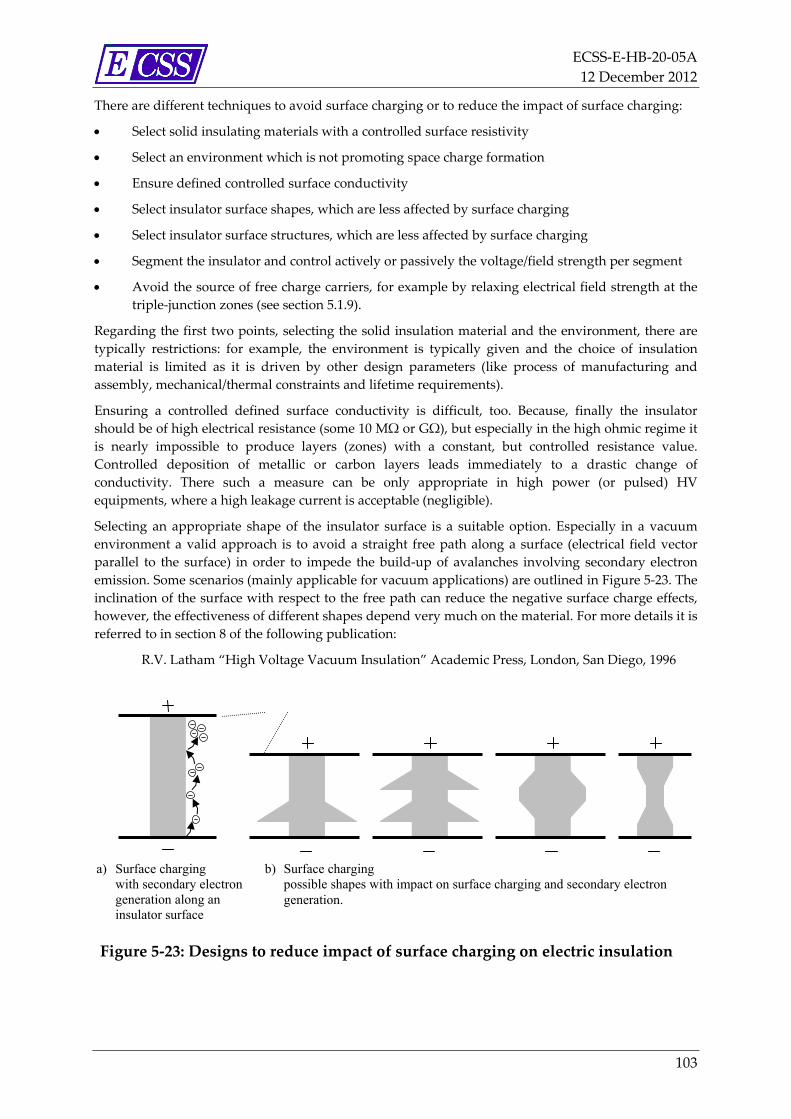
ECSS‐E‐HB‐20‐05A
12 December 2012
103
There are different techniques to avoid surface charging or to reduce the impact of surface charging:
Select solid insulating materials with a controlled surface resistivity
Select an environment which is not promoting space charge formation
Ensure defined controlled surface conductivity
Select insulator surface shapes, which are less affected by surface charging
Select insulator surface structures, which are less affected by surface charging
Segment the insulator and control actively or passively the voltage/field strength per segment
Avoid the source of free charge carriers, for example by relaxing electrical field strength at the
triple‐junction zones (see section 5.1.9).
Regarding the first two points, selecting the solid insulation material and the environment, there are
typically restrictions: for example, the environment is typically given and the choice of insulation
material is limited as it is driven by other design parameters (like process of manufacturing and
assembly, mechanical/thermal constraints and lifetime requirements).
Ensuring a controlled defined surface conductivity is difficult, too. Because, finally the insulator
should be of high electrical resistance (some 10 MΩ or GΩ), but especially in the high ohmic regime it
is nearly impossible to produce layers (zones) with a constant, but controlled resistance value.
Controlled deposition of metallic or carbon layers leads immediately to a drastic change of
conductivity. There such a measure can be only appropriate in high power (or pulsed) HV
equipments, where a high leakage current is acceptable (negligible).
Selecting an appropriate shape of the insulator surface is a suitable option. Especially in a vacuum
environment a valid approach is to avoid a straight free path along a surface (electrical field vector
parallel to the surface) in order to impede the build‐up of avalanches involving secondary electron
emission. Some scenarios (mainly applicable for vacuum applications) are outlined in Figure 5‐23. The
inclination of the surface with respect to the free path can reduce the negative surface charge effects,
however, the effectiveness of different shapes depend very much on the material. For more details it is
referred to in section 8 of the following publication:
R.V. Latham “High Voltage Vacuum Insulation” Academic Press, London, San Diego, 1996
Figure 5‐23: Designs to reduce impact of surface charging on electric insulation
a) Surface charging with secondary electrongeneration along an insulator surface
b) Surface charging possible shapes with impact on surface charging and secondary electron generation.
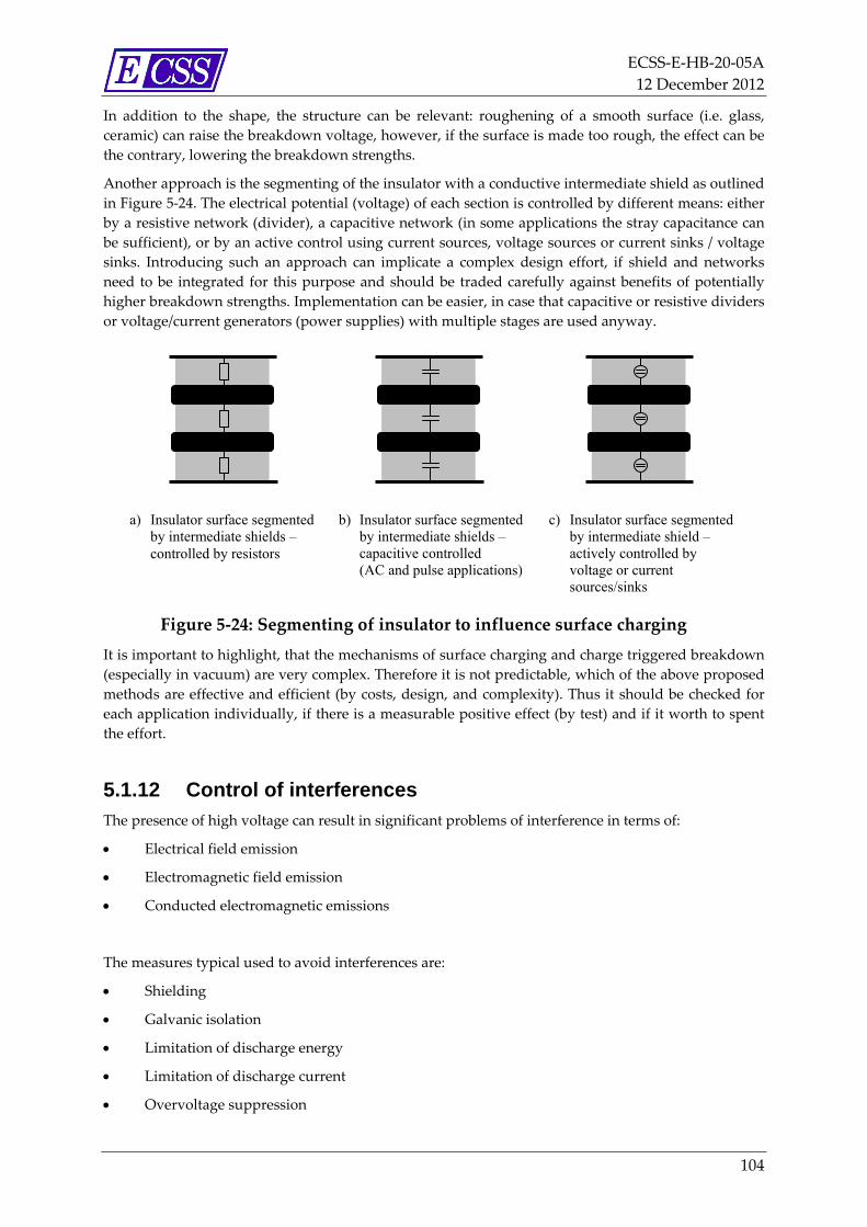
ECSS‐E‐HB‐20‐05A
12 December 2012
104
In addition to the shape, the structure can be relevant: roughening of a smooth surface (i.e. glass,
ceramic) can raise the breakdown voltage, however, if the surface is made too rough, the effect can be
the contrary, lowering the breakdown strengths.
Another approach is the segmenting of the insulator with a conductive intermediate shield as outlined
in Figure 5‐24. The electrical potential (voltage) of each section is controlled by different means: either
by a resistive network (divider), a capacitive network (in some applications the stray capacitance can
be sufficient), or by an active control using current sources, voltage sources or current sinks / voltage
sinks. Introducing such an approach can implicate a complex design effort, if shield and networks
need to be integrated for this purpose and should be traded carefully against benefits of potentially
higher breakdown strengths. Implementation can be easier, in case that capacitive or resistive dividers
or voltage/current generators (power supplies) with multiple stages are used anyway.
Figure 5‐24: Segmenting of insulator to influence surface charging
It is important to highlight, that the mechanisms of surface charging and charge triggered breakdown
(especially in vacuum) are very complex. Therefore it is not predictable, which of the above proposed
methods are effective and efficient (by costs, design, and complexity). Thus it should be checked for
each application individually, if there is a measurable positive effect (by test) and if it worth to spent
the effort.
5.1.12 Control of interferences
The presence of high voltage can result in significant problems of interference in terms of:
Electrical field emission
Electromagnetic field emission
Conducted electromagnetic emissions
The measures typical used to avoid interferences are:
Shielding
Galvanic isolation
Limitation of discharge energy
Limitation of discharge current
Overvoltage suppression
a) Insulator surface segmented by intermediate shields – controlled by resistors
b) Insulator surface segmented by intermediate shields – capacitive controlled (AC and pulse applications)
c) Insulator surface segmented by intermediate shield – actively controlled by voltage or current sources/sinks
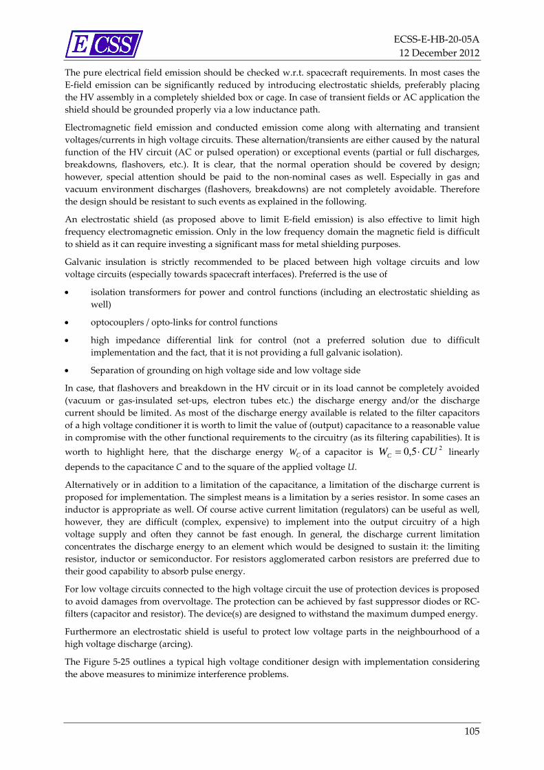
ECSS‐E‐HB‐20‐05A
12 December 2012
105
The pure electrical field emission should be checked w.r.t. spacecraft requirements. In most cases the
E‐field emission can be significantly reduced by introducing electrostatic shields, preferably placing
the HV assembly in a completely shielded box or cage. In case of transient fields or AC application the
shield should be grounded properly via a low inductance path.
Electromagnetic field emission and conducted emission come along with alternating and transient
voltages/currents in high voltage circuits. These alternation/transients are either caused by the natural
function of the HV circuit (AC or pulsed operation) or exceptional events (partial or full discharges,
breakdowns, flashovers, etc.). It is clear, that the normal operation should be covered by design;
however, special attention should be paid to the non‐nominal cases as well. Especially in gas and
vacuum environment discharges (flashovers, breakdowns) are not completely avoidable. Therefore
the design should be resistant to such events as explained in the following.
An electrostatic shield (as proposed above to limit E‐field emission) is also effective to limit high
frequency electromagnetic emission. Only in the low frequency domain the magnetic field is difficult
to shield as it can require investing a significant mass for metal shielding purposes.
Galvanic insulation is strictly recommended to be placed between high voltage circuits and low
voltage circuits (especially towards spacecraft interfaces). Preferred is the use of
isolation transformers for power and control functions (including an electrostatic shielding as
well)
optocouplers / opto‐links for control functions
high impedance differential link for control (not a preferred solution due to difficult
implementation and the fact, that it is not providing a full galvanic isolation).
Separation of grounding on high voltage side and low voltage side
In case, that flashovers and breakdown in the HV circuit or in its load cannot be completely avoided
(vacuum or gas‐insulated set‐ups, electron tubes etc.) the discharge energy and/or the discharge
current should be limited. As most of the discharge energy available is related to the filter capacitors
of a high voltage conditioner it is worth to limit the value of (output) capacitance to a reasonable value
in compromise with the other functional requirements to the circuitry (as its filtering capabilities). It is
worth to highlight here, that the discharge energy CW of a capacitor is 25,0 CUWC linearly
depends to the capacitance C and to the square of the applied voltage U.
Alternatively or in addition to a limitation of the capacitance, a limitation of the discharge current is
proposed for implementation. The simplest means is a limitation by a series resistor. In some cases an
inductor is appropriate as well. Of course active current limitation (regulators) can be useful as well,
however, they are difficult (complex, expensive) to implement into the output circuitry of a high
voltage supply and often they cannot be fast enough. In general, the discharge current limitation
concentrates the discharge energy to an element which would be designed to sustain it: the limiting
resistor, inductor or semiconductor. For resistors agglomerated carbon resistors are preferred due to
their good capability to absorb pulse energy.
For low voltage circuits connected to the high voltage circuit the use of protection devices is proposed
to avoid damages from overvoltage. The protection can be achieved by fast suppressor diodes or RC‐
filters (capacitor and resistor). The device(s) are designed to withstand the maximum dumped energy.
Furthermore an electrostatic shield is useful to protect low voltage parts in the neighbourhood of a
high voltage discharge (arcing).
The Figure 5‐25 outlines a typical high voltage conditioner design with implementation considering
the above measures to minimize interference problems.
ECSS‐E‐HB‐20‐05A
12 December 2012
106
Figure 5‐25: Implementation of design measures minimizing interference
problems for a typical high voltage power conditioner (regulated DC‐DC
converter for high voltage as an example)
Possible interference protection measures
HV
rectifier
HV
filterHV
divider
HV
transformer
Control Circuit
(Low voltage circuit
referenced to HV‐
ground
Low voltage
input circuit
Current
limiting
resistor
Suppressor Optocoupler
HV
load
1
1
2
2
4
3
3
4
5 6
7
9
8
5
6
7
8
9
10
10
HV insulation
Shield (metal or metallised)
Transformer for galvanic isolation of power path
Optocoupler for galvanic isolation of signal path
Electrostatic shield between primary and secondary
Limitation of discharge energy (max. C)
Secondary ground on HV side separate from low voltage side
Suppressor circuits to protect low voltage devices from overvoltage
Electrostatic shield for connection to load
Limitation of discharge current by resistor
ECSS‐E‐HB‐20‐05A
12 December 2012
107
5.2 High voltage assemblies
5.2.1 Solid insulation: potted modules
5.2.1.1 General
For space applications the most widely used type of solid insulation is the potted insulation forming
the:
potted modules
The advantages of such potted insulations are their capability:
to embed and isolate complex assemblies, as printed circuit boards and transformers
to provide a mechanically stabilized encapsulation
to allow multiple encapsulations in a sequence (typically)
to avoid space vacuum related effects, ground related effects (ambient atmosphere) and
transition effects (between both) ‐if adequately designed
to provide a good thermal interface (depending on the selected material)
to provide a compact design (size) due to high insulation strengths
Their disadvantages can be found in their
mass
sensitivity to thermo‐mechanical ageing and partial discharges
However, these disadvantages can be compensated by an optimization of the shape (to optimize
mass), a proper design (to minimize thermo/mechanical ageing effects) and suitable potting process
(to avoid any local areas affected by partial discharges).
5.2.1.2 Materials
5.2.1.2.1 Overview
In general, there are three classes of potting materials acceptable for use in spacecraft:
epoxy resin‐based materials
silicone materials
polyurethane (PUR) materials
From, each of these groups there are candidates available, which show a low outgassing rate, being
compatible with contamination requirements. All mentioned materials are belonging to the chemical
group of polymer materials formed by large structures of organic molecules.
Epoxy and PUR belong to the class of thermosetting resins, forming an inherently stable material after
curing. Silicone resins typically form an elastic material after curing (rubber‐type elastomer).
Potting materials allow compact designs enabling high field strengths inside of the insulation. As a
consequence, the insulation should be free of defects, especially free of voids, cracks, delaminations
and particles. Such defects are a source accelerating ageing and limiting lifetime. Partial discharges are
a very relevant part of the ageing mechanism under AC voltage, but also a non negligible ageing

ECSS‐E‐HB‐20‐05A
12 December 2012
108
contributor for DC and pulsed voltage. In order to minimize the risk of degradation by insulation
defects the design of potted high voltage modules and the potting process needs to be adequate and
well defined.
The processing of the potting material typical involves the mixing and processing of different
components, at least
the resin (not cured)
a curing agent (hardener)
and for many resin products additives as
flexibilisators
accelerators (for curing)
fillers.
Some commercial products are offered as pre‐mixture of at least a 2‐component system or a 3‐
component system. Often a user is optimizing his ”own” resin composition of multiple components.
A brief summary on the different materials is given in the following.
5.2.1.2.2 Epoxy Resins (EP)
Epoxy resins are molecules containing C2H3O groups (epoxy groups) at the end of each molecule
chain. The quantity of epoxy groups is expressed by the so called EEW value, the epoxy equivalent
weight. It describes the quantity of resin in grams which contains 1mol oxygen (of epoxy groups).
Resins of low viscosity have EEWs of less than 200 g.
Two groups of epoxy resins have become more dominant for high voltage applications. The bisphenol
Resins are mainly used for indoor insulation whereas cycloaliphatic resins are used for outdoor
insulation.
Furthermore, it is distinguished between epoxy resins hardening at high temperatures by anhydride
hardeners and epoxy resins hardening at about room temperature by amine and amide hardeners. For
long‐term high voltage applications it is preferred to use the anhydride hardened epoxies.
Epoxy resins are used often with fillers. For space applications the typical filling material is a quartz
powder (silica powder). The purpose of the filler is to
match the thermo‐mechanical expansion coefficient with the embedded components,
increase heat conductivity
reduce the material shrinkage effect during curing.
The filler needs to be very well optimized with the resin to ensure the proper viscosity for moulding
and to avoid sedimentation during curing. A well optimized mixture of different glass particle sizes is
important. The use of “silanized” fillers ensures that the particle surface is hydrophobic and thus
dielectric properties are not worsened by humidity.
The unfilled epoxy material is transparent in most of the cases, which makes it easier to detect defects
and void after processing, which is typically not possible by visible inspection with filled epoxy
materials.
Other new minerally filled epoxy systems are still under development and actually not in use for
space applications: as the use of “core shell tougheners” to reduce cracks and fractures under
mechanical shock and the use of nanotechnology and nano‐materials (n‐fillers).
ECSS‐E‐HB‐20‐05A
12 December 2012
109
The main assets of epoxy materials are their excellent electrical properties, good mechanical
properties, low water absorption, good adhesion to metals, and low mould shrinkage. Furthermore,
they have a low outgassing characteristics and low vapour pressure. These properties are affected by
treatment and processing technique.
5.2.1.2.3 Silicone Resins (SIR)
Silicones are water repellent, heat stable, and very resistant to chemicals. Silicone polymers offer
superior electrical properties and excellent thermal properties especially in terms of a low degradation
at high temperatures. Main applications of silicon elastomer are curing and potting and flexible
insulations, i.e. cables. As the material is a “rubber” it is usually soft and therefore it is not suitable for
exposure to high mechanical loads.
Silicones used for insulation purposes have a good resistance against partial discharges and X‐ray. A
problem is the insufficient adhesion to metals and other organic materials which can be improved by
using primers.
The outgassing of silicones is an area of concern especially for space applications. Newer formulas
with less low molecular weight siloxane molecule groups can reduce the mass loss significantly.
Potting materials of this type are extremely expensive and therefore are suitable only for small volume
applications.
5.2.1.2.4 Polyurethanes (PUR)
Polyurethane is a polymer consisting of a chain of organic molecule groups joined by urethane links
Polyurethane (PU) is produced in a variety of textures and harnesses by varying the particular
monomers and adding other substances. Softer polyurethane can be made by adding flexible
Polyethylene glycol segments between urethane links.
Careful control of viscoelastic properties can lead to memory foam, which is much softer at skin
temperature than at room temperature. Polyurethane foam (including foam rubber) can be produced
by adding a small amount of water to one of the liquid precursors of polyurethane before they are
mixed together. This modifies the polymerisation reaction, causing carbon dioxide to be released as
the material cures. Gas is generated throughout the liquid, creating relatively uniform bubbles which
then harden to form solid foam as polymerisation progresses. However, the use of foams is critical for
high voltage insulation due to their “natural” content of void featuring partial discharges.
Therefore the typical PUR application for high voltage insulation in space applications is PUR as an
inherently stable thermoset material. Low glass transition temperature, good electrical values and
very good reparability makes the PUs suitable for the potting of high voltage components in a
temperature range of –50 °C to +120 °C. Nevertheless many unfilled polyurethanes have problems to
comply with typical outgassing requirements of spacecraft. Another critical point is the temperature
resistance or the ageing of PU under the presence of oxygen.
Additional characteristics of the polyurethanes comprise good electric properties (in terms of high
voltage dielectric strengths), a good adhesion to most materials, low exothermic temperature rise
during curing, low mould shrinkage, long pot life, and easy reparability. The linear thermal coefficient
of expansion is greater than epoxies but smaller than the silicones.
A typical encapsulation problem is the mechanical stress developed between the encapsulant and the
embedded parts due to elevated temperatures, temperature differences, and encapsulant shrinkage. In
many applications the use of fillers can be helpful to bring different mechanical properties in
agreement. In general the fillers increase the value of thermal conductivity and decrease thermal
expansion.
The handling of the polyurethanes should be performed with care since the pre‐polymers and curing
agents can be health hazardous.

ECSS‐E‐HB‐20‐05A
12 December 2012
110
5.2.1.2.5 Fillers
In high voltage applications inorganic fillers are used in casting resins where they fulfil various
functions:
improvement of mechanical properties like CTE (coefficient of thermal expansion), elastic
modulus, hardness, tensile strength, elongation at break
influence on the electrical properties like dielectric constant and dissipation factor, resistivity,
dielectric strength
reduction of exothermic reaction during curing process
improvement of thermal properties like of thermal conductivity, thermal expansion and
capacity
cost reduction of cast resins (important for large volume applications).
Density and particle size are the most important parameters. In practice fillers with a particle size of
less than 50 μm (μ‐fillers) are often used. Popular fillers are quartz/silica, quartz/silica based materials,
alumina and glass fibres.
Regarding ageing effects the internal interface between filler and resin plays an important role. The
quality of the insulation system depends evidently on the adhesion between filler and resin. A low
adhesion leads to accelerated ageing processes caused by moisture, partial discharges and
electromechanical forces. These effects can be classified by loss factor measurements and partial
discharge analysis.
These ageing mechanisms related to interfacial phenomena can be influenced by special preparation
of the fillers and filler surfaces. Examples are:
hydrophobic additives (silane treatment)
additives to improve adhesion
plasma treating
‘pure’ filler with low impurities.
Most important fillers are quartz/silica powder often improved by silane treatment. Other (for space
applications less relevant) fillers are wollastonit and chalk which are cheap in production. New types
of fillers like boron nitride or aluminium nitride, which are not very common in use and (today) not
offered as established mixture from the available suppliers. Users, which are interested in resin
trimmed with these “sophisticated” fillers, have the choice either to develop the filled system
themselves or to request this from specialized industrial service providers.
A new interesting family of fillers are the nano‐scaled fillers (n‐fillers). Particle sizes from 1 nm to
100 nm are achieved and new insulation systems are still under development.
Advantageous effects of nano‐materials are related to microscopic interactions between the surface of
the filler particles and the resin. The smaller the particle size the more atoms are located on the
surface. Particles with diameter of 20 nm contain 10 % of the atoms at the surface and 1nm particles
contain 99 % of the atoms at the surface. This results in a stronger interfacial linkage between the
atoms on the particle surface to atoms in the particle and atoms of the resin. Concluding, even with
low filler content (10 % ‐ 30 %) the physical properties of the composed material can change
significantly.
With the small size of the n‐fillers the more important become the proper mixing between filler and
resin. Only with special high speed mixers it is possible to achieve a smooth dispersion. For analysis
(particle distribution) and characterisation of the filled system only REM and TEM with highest
resolution, X‐ray structure analysis and high sophisticated optical methods can be used.
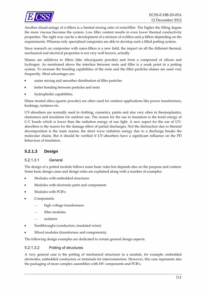
ECSS‐E‐HB‐20‐05A
12 December 2012
111
Another disadvantage of n‐fillers is a limited mixing ratio of resin/filler. The higher the filling degree
the more viscous becomes the system. Low filler content results in even lower thermal conductivity
properties. The right way can be a development of a mixture of n‐fillers and μ‐fillers depending on the
requirements. Whereas only specialised companies are able to develop such a filled potting system.
Since research on composites with nano‐fillers is a new field, the impact on all the different thermal,
mechanical and electrical properties is not very well known, actually.
Silanes are additives to fillers (like silica/quartz powder) and form a compound of silicon and
hydrogen. As mentioned above the interface between resin and filler is a weak point in a potting
system. To increase the bonding capabilities of the resin and the filler particles silanes are used very
frequently. Most advantages are:
easier mixing and smoother distribution of filler particles
better bonding between particles and resin
hydrophobic capabilities.
Silane treated silica (quartz powder) are often used for outdoor applications like power transformers,
bushings, isolators etc.
UV‐absorbers are normally used in clothing, cosmetics, paints and also very often in thermoplastics,
elastomers and insulators for outdoor use. The reason for the use in insulators is the bond energy of
C‐C bonds which is lower than the radiation energy of sun light. A new aspect for the use of UV‐
absorbers is the reason for the damage effect of partial discharges. Not the destruction due to thermal
decomposition is the main reason; the short wave radiation energy due to a discharge breaks the
molecular chains. But it should be verified if UV‐absorbers have a significant influence on the PD
behaviour of insulators.
5.2.1.3 Design
5.2.1.3.1 General
The design of a potted module follows some basic rules but depends also on the purpose and content.
Some basic design cases and design rules are explained along with a number of examples:
Modules with embedded structures
Modules with electronic parts and components
Modules with PCB’s
Components
high voltage transformers
filter modules
isolators
Feedthroughs (conductors, insulated wires)
Mixed modules (transformer and components).
The following design examples are dedicated to certain general design aspects.
5.2.1.3.2 Potting of structures
A very general case is the potting of mechanical structures in a module, for example: embedded
electrodes, embedded conductors or terminals for interconnection. However, this case represents also
the packaging of more complex assemblies with HV components and PCB’s.
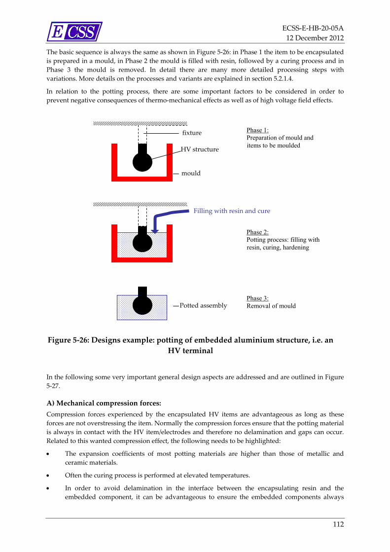
ECSS‐E‐HB‐20‐05A
12 December 2012
112
The basic sequence is always the same as shown in Figure 5‐26: in Phase 1 the item to be encapsulated
is prepared in a mould, in Phase 2 the mould is filled with resin, followed by a curing process and in
Phase 3 the mould is removed. In detail there are many more detailed processing steps with
variations. More details on the processes and variants are explained in section 5.2.1.4.
In relation to the potting process, there are some important factors to be considered in order to
prevent negative consequences of thermo‐mechanical effects as well as of high voltage field effects.
Figure 5‐26: Designs example: potting of embedded aluminium structure, i.e. an
HV terminal
In the following some very important general design aspects are addressed and are outlined in Figure
5‐27.
A) Mechanical compression forces:
Compression forces experienced by the encapsulated HV items are advantageous as long as these
forces are not overstressing the item. Normally the compression forces ensure that the potting material
is always in contact with the HV item/electrodes and therefore no delamination and gaps can occur.
Related to this wanted compression effect, the following needs to be highlighted:
The expansion coefficients of most potting materials are higher than those of metallic and
ceramic materials.
Often the curing process is performed at elevated temperatures.
In order to avoid delamination in the interface between the encapsulating resin and the
embedded component, it can be advantageous to ensure the embedded components always
mould
fixture
HV structure
Filling with resin and cure
Phase 1: Preparation of mould and items to be moulded
Phase 2: Potting process: filling with resin, curing, hardening
Phase 3: Removal of mould Potted assembly
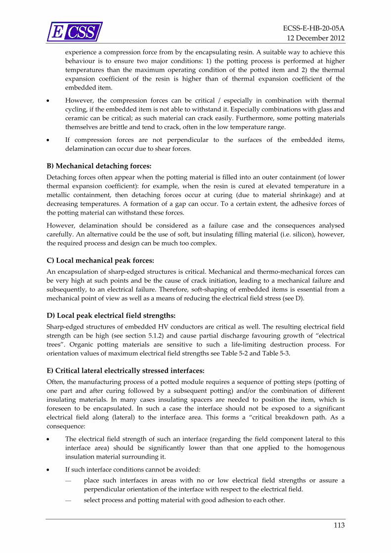
ECSS‐E‐HB‐20‐05A
12 December 2012
113
experience a compression force from by the encapsulating resin. A suitable way to achieve this
behaviour is to ensure two major conditions: 1) the potting process is performed at higher
temperatures than the maximum operating condition of the potted item and 2) the thermal
expansion coefficient of the resin is higher than of thermal expansion coefficient of the
embedded item.
However, the compression forces can be critical / especially in combination with thermal
cycling, if the embedded item is not able to withstand it. Especially combinations with glass and
ceramic can be critical; as such material can crack easily. Furthermore, some potting materials
themselves are brittle and tend to crack, often in the low temperature range.
If compression forces are not perpendicular to the surfaces of the embedded items,
delamination can occur due to shear forces.
B) Mechanical detaching forces:
Detaching forces often appear when the potting material is filled into an outer containment (of lower
thermal expansion coefficient): for example, when the resin is cured at elevated temperature in a
metallic containment, then detaching forces occur at curing (due to material shrinkage) and at
decreasing temperatures. A formation of a gap can occur. To a certain extent, the adhesive forces of
the potting material can withstand these forces.
However, delamination should be considered as a failure case and the consequences analysed
carefully. An alternative could be the use of soft, but insulating filling material (i.e. silicon), however,
the required process and design can be much too complex.
C) Local mechanical peak forces:
An encapsulation of sharp‐edged structures is critical. Mechanical and thermo‐mechanical forces can
be very high at such points and be the cause of crack initiation, leading to a mechanical failure and
subsequently, to an electrical failure. Therefore, soft‐shaping of embedded items is essential from a
mechanical point of view as well as a means of reducing the electrical field stress (see D).
D) Local peak electrical field strengths:
Sharp‐edged structures of embedded HV conductors are critical as well. The resulting electrical field
strength can be high (see section 5.1.2) and cause partial discharge favouring growth of “electrical
trees”. Organic potting materials are sensitive to such a life‐limiting destruction process. For
orientation values of maximum electrical field strengths see Table 5‐2 and Table 5‐3.
E) Critical lateral electrically stressed interfaces:
Often, the manufacturing process of a potted module requires a sequence of potting steps (potting of
one part and after curing followed by a subsequent potting) and/or the combination of different
insulating materials. In many cases insulating spacers are needed to position the item, which is
foreseen to be encapsulated. In such a case the interface should not be exposed to a significant
electrical field along (lateral) to the interface area. This forms a “critical breakdown path. As a
consequence:
The electrical field strength of such an interface (regarding the field component lateral to this
interface area) should be significantly lower than that one applied to the homogenous
insulation material surrounding it.
If such interface conditions cannot be avoided:
place such interfaces in areas with no or low electrical field strengths or assure a
perpendicular orientation of the interface with respect to the electrical field.
select process and potting material with good adhesion to each other.
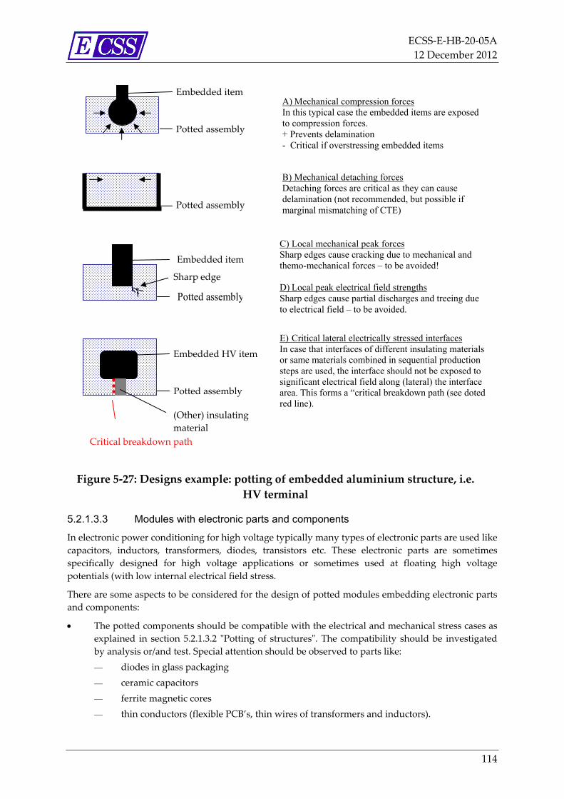
ECSS‐E‐HB‐20‐05A
12 December 2012
114
Figure 5‐27: Designs example: potting of embedded aluminium structure, i.e.
HV terminal
5.2.1.3.3 Modules with electronic parts and components
In electronic power conditioning for high voltage typically many types of electronic parts are used like
capacitors, inductors, transformers, diodes, transistors etc. These electronic parts are sometimes
specifically designed for high voltage applications or sometimes used at floating high voltage
potentials (with low internal electrical field stress.
There are some aspects to be considered for the design of potted modules embedding electronic parts
and components:
The potted components should be compatible with the electrical and mechanical stress cases as
explained in section 5.2.1.3.2 ʺPotting of structuresʺ. The compatibility should be investigated
by analysis or/and test. Special attention should be observed to parts like:
diodes in glass packaging
ceramic capacitors
ferrite magnetic cores
thin conductors (flexible PCB’s, thin wires of transformers and inductors).
A) Mechanical compression forces In this typical case the embedded items are exposed to compression forces. + Prevents delamination - Critical if overstressing embedded items
Potted assembly
B) Mechanical detaching forces Detaching forces are critical as they can cause delamination (not recommended, but possible if marginal mismatching of CTE) Potted assembly
Embedded item
C) Local mechanical peak forces Sharp edges cause cracking due to mechanical and themo-mechanical forces – to be avoided! D) Local peak electrical field strengths Sharp edges cause partial discharges and treeing due to electrical field – to be avoided.
Potted assembly
Embedded item
E) Critical lateral electrically stressed interfaces In case that interfaces of different insulating materials or same materials combined in sequential production steps are used, the interface should not be exposed to significant electrical field along (lateral) the interface area. This forms a “critical breakdown path (see doted red line).
Potted assembly
Embedded HV item
Sharp edge
(Other) insulating
material
Critical breakdown path
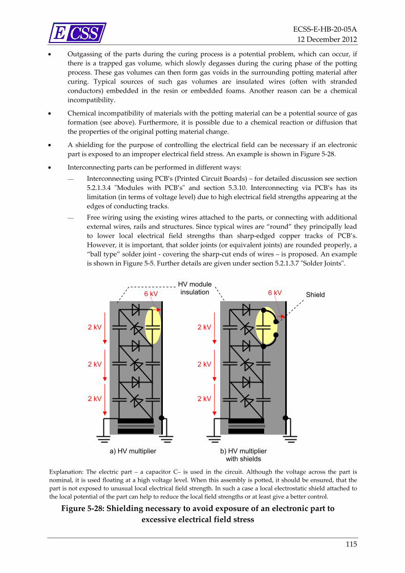
ECSS‐E‐HB‐20‐05A
12 December 2012
115
Outgassing of the parts during the curing process is a potential problem, which can occur, if
there is a trapped gas volume, which slowly degasses during the curing phase of the potting
process. These gas volumes can then form gas voids in the surrounding potting material after
curing. Typical sources of such gas volumes are insulated wires (often with stranded
conductors) embedded in the resin or embedded foams. Another reason can be a chemical
incompatibility.
Chemical incompatibility of materials with the potting material can be a potential source of gas
formation (see above). Furthermore, it is possible due to a chemical reaction or diffusion that
the properties of the original potting material change.
A shielding for the purpose of controlling the electrical field can be necessary if an electronic
part is exposed to an improper electrical field stress. An example is shown in Figure 5‐28.
Interconnecting parts can be performed in different ways:
Interconnecting using PCB’s (Printed Circuit Boards) – for detailed discussion see section
5.2.1.3.4 ʺModules with PCB’sʺ and section 5.3.10. Interconnecting via PCB’s has its
limitation (in terms of voltage level) due to high electrical field strengths appearing at the
edges of conducting tracks.
Free wiring using the existing wires attached to the parts, or connecting with additional
external wires, rails and structures. Since typical wires are “round” they principally lead
to lower local electrical field strengths than sharp‐edged copper tracks of PCB’s.
However, it is important, that solder joints (or equivalent joints) are rounded properly, a
“ball type” solder joint ‐ covering the sharp‐cut ends of wires – is proposed. An example
is shown in Figure 5‐5. Further details are given under section 5.2.1.3.7 ʺSolder Jointsʺ.
Explanation: The electric part – a capacitor C– is used in the circuit. Although the voltage across the part is
nominal, it is used floating at a high voltage level. When this assembly is potted, it should be ensured, that the
part is not exposed to unusual local electrical field strength. In such a case a local electrostatic shield attached to
the local potential of the part can help to reduce the local field strengths or at least give a better control.
Figure 5‐28: Shielding necessary to avoid exposure of an electronic part to
excessive electrical field stress
a) HV multiplier
HV module insulation
2 kV
2 kV
2 kV
6 kV
b) HV multiplier with shields
6 kV Shield
2 kV
2 kV
2 kV
ECSS‐E‐HB‐20‐05A
12 December 2012
116
5.2.1.3.4 Modules with PCB’s
Potting of PCB’s – rigid or flexible ‐ is a practical method to simplify the production process, but can
lead to a complex thermo‐mechanical design, especially if different types of electrical components are
soldered onto the PCB. Typically, local stress cases and the influence of thermo‐cycling on lifetime
cannot be easily predicted; therefore thermo‐cycling with the applicable load cases together with the
high voltage stress is essential.
From a pure electrical point of view, there are different design cases to be considered:
The circuit on the PCB is “low voltage”, but everything is electrically floating and associated to
a high voltage potential. Between tracks – inter‐layer and intra‐layer – the voltage is low. In
such cases high electrical field strength can appear only on the boundary tracks to the outside.
Local shielding or global shielding is needed, if local electrical field strength is too high (see
Figure 5‐28‐b for global shielding and for local shielding Figure 5‐29).
The circuit on the PCB is carrying “high voltage”. In this case local shielding is needed, if local
electrical field strengths are too high (see Figure 5‐29 A‐D). Furthermore, cut‐outs in the PCB
can help to improve the interface between PCB and potting material (see Figure 5‐29 E,F)
Additional information is given in section 5.3.10.
Potting of a PCB typically requires surface treatment to control adhesion of the resin to the PCB
assembly (see section 5.2.1.4).
Furthermore, it is pointed out, that instead of complete potting of PCB’s in some applications coatings
or condensed layers are used (see section 5.3.10).
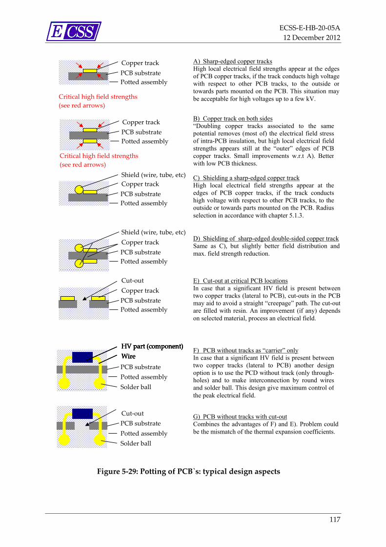
ECSS‐E‐HB‐20‐05A
12 December 2012
117
Figure 5‐29: Potting of PCB`s: typical design aspects
A) Sharp-edged copper tracks High local electrical field strengths appear at the edges of PCB copper tracks, if the track conducts high voltage with respect to other PCB tracks, to the outside or towards parts mounted on the PCB. This situation may be acceptable for high voltages up to a few kV.
Potted assembly
PCB substrate
Critical high field strengths
(see red arrows)
Copper track
B) Copper track on both sides “Doubling copper tracks associated to the same potential removes (most of) the electrical field stress of intra-PCB insulation, but high local electrical field strengths appears still at the “outer” edges of PCB copper tracks. Small improvements w.r.t A). Better with low PCB thickness.
C) Shielding a sharp-edged copper track High local electrical field strengths appear at the edges of PCB copper tracks, if the track conducts high voltage with respect to other PCB tracks, to the outside or towards parts mounted on the PCB. Radius selection in accordance with chapter 5.1.3.
Potted assembly
PCB substrate
Copper track
Potted assembly
PCB substrate
Critical high field strengths
(see red arrows)
Copper track
D) Shielding of sharp-edged double-sided copper trackSame as C), but slightly better field distribution andmax. field strength reduction.
Potted assembly
PCB substrate
Copper track
Shield (wire, tube, etc)
Shield (wire, tube, etc)
E) Cut-out at critical PCB locations In case that a significant HV field is present between two copper tracks (lateral to PCB), cut-outs in the PCB may aid to avoid a straight “creepage” path. The cut-out are filled with resin. An improvement (if any) depends on selected material, process an electrical field.
Potted assembly
PCB substrate
Copper track
Cut‐out
Potted assembly
PCB substrate
Solder ball
Potted assembly
PCB substrate
Solder ball
Cut‐out G) PCB without tracks with cut-out Combines the advantages of F) and E). Problem could be the mismatch of the thermal expansion coefficients.
F) PCB without tracks as “carrier” only In case that a significant HV field is present between two copper tracks (lateral to PCB) another design option is to use the PCD without track (only through-holes) and to make interconnection by round wires and solder ball. This design give maximum control of the peak electrical field.
Wire
HV part (component)
Wire
HV part (component)
Wire
HV part (component)
Wire
HV part (component)
Wire
HV part (component)
Wire
HV part (component)
ECSS‐E‐HB‐20‐05A
12 December 2012
118
5.2.1.3.5 Components
Typical components used in high voltage electronics are:
HV transformers
filter modules
Both are typical parts of high voltage power conditioners used in space electronics. A transformer to
step‐up from low voltage to high voltage using high frequency AC voltage (often between few ten kHz
and few hundred kHz) and a rectifier/filter module to produce a “smooth” DC voltage.
For completeness, it should be emphasized here, that the combination of a HV transformer and a HV
filter module is an example for any other combination of high voltage function integrated into
modules. So the presented considerations are transferable to many other combinations of components
and modules.
High voltage transformers and filter modules can be built as potted modules or partially potted. Non‐
potted alternatives are either limited to the lower high voltage range (few hundred volts and non
subject to Paschen breakdown) or need to involve other high voltage insulations like oil or pressurized
gas (however, both methods are not well established in space environments. More detailed aspects of
these topics can be found in sections 4.2.3, 5.3.1, and 5.3.8.
As both components are used together with an electrical interface, there are some design options for
potting.
Two different modules in “open” connection (see Figure 5‐30)
The advantage is an individual potting of each module (one filter, one transformer), which can
be very well matched to the embedded items. Thermo‐mechanical stresses and the risk of
encapsulating a defect is less critical due to lower potted volume (compared to combing both in
one module). Furthermore it is easily possible to test each module individually for function,
performance and high voltage insulation. Good reparability and maintainability can be
obtained as each module. Can easily be exchanged
Disadvantages are higher mass, size and the need for “open” terminal for interconnection.
Furthermore the modules need an “outer” insulating environment as gas, liquid or vacuum.
Two different modules with potted HV harness (see Figure 5‐31)
Similar configuration as above, however, the interconnecting high voltage harness is potted,
thus the outer environments do not play an important role for overall insulation. This
independence of the environment is at the expense of a more complex potting sequence: either
the modules are potted individually and only the interconnecting harness is potted in a second
step, or the harness is potted in the same step (which comes close to the situation described
below “Common module”).
When the harness is potted in a second step, there is typically the need for a small mould. Often
it is possible to foresee a “niche” in the potted module which fulfils the function of a “natural”
mould; otherwise it is necessary to place an external mould with sealing.
It is obvious, that the disconnection of the potted harness can be difficult or not possible at all. If
soft potting materials (like silicone or soft polyurethane) are used, it is easier to make the
connection accessible again by removing material, thus rendering the connection point
accessible and after repair, allow re‐potting of the connection.
Regarding the harness treatment see also 5.3.5. The design of the harness potting needs to
respect sufficient strain in order to avoid detachments and delamination of the harness
insulation from the surrounding potting material. Furthermore, it is typically the case, that the
harness needs special treatment (cleaning, etching etc.) to ensure proper interfacing with a
potting material. In addition, it is worth consideration that the harnesses typically have some
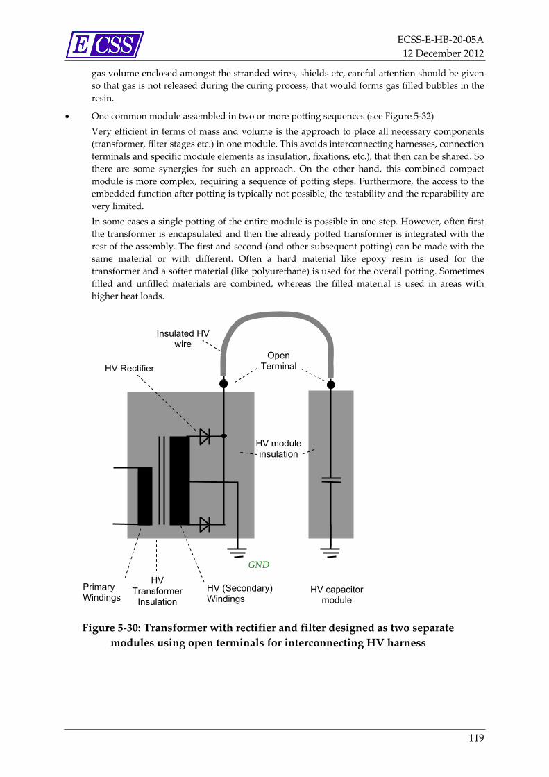
ECSS‐E‐HB‐20‐05A
12 December 2012
119
gas volume enclosed amongst the stranded wires, shields etc, careful attention should be given
so that gas is not released during the curing process, that would forms gas filled bubbles in the
resin.
One common module assembled in two or more potting sequences (see Figure 5‐32)
Very efficient in terms of mass and volume is the approach to place all necessary components
(transformer, filter stages etc.) in one module. This avoids interconnecting harnesses, connection
terminals and specific module elements as insulation, fixations, etc.), that then can be shared. So
there are some synergies for such an approach. On the other hand, this combined compact
module is more complex, requiring a sequence of potting steps. Furthermore, the access to the
embedded function after potting is typically not possible, the testability and the reparability are
very limited.
In some cases a single potting of the entire module is possible in one step. However, often first
the transformer is encapsulated and then the already potted transformer is integrated with the
rest of the assembly. The first and second (and other subsequent potting) can be made with the
same material or with different. Often a hard material like epoxy resin is used for the
transformer and a softer material (like polyurethane) is used for the overall potting. Sometimes
filled and unfilled materials are combined, whereas the filled material is used in areas with
higher heat loads.
Figure 5‐30: Transformer with rectifier and filter designed as two separate
modules using open terminals for interconnecting HV harness
GND
Primary Windings
HV (Secondary)Windings
HV Transformer
Insulation HV capacitor
module
HV Rectifier
Insulated HV wire
HV module insulation
Open Terminal
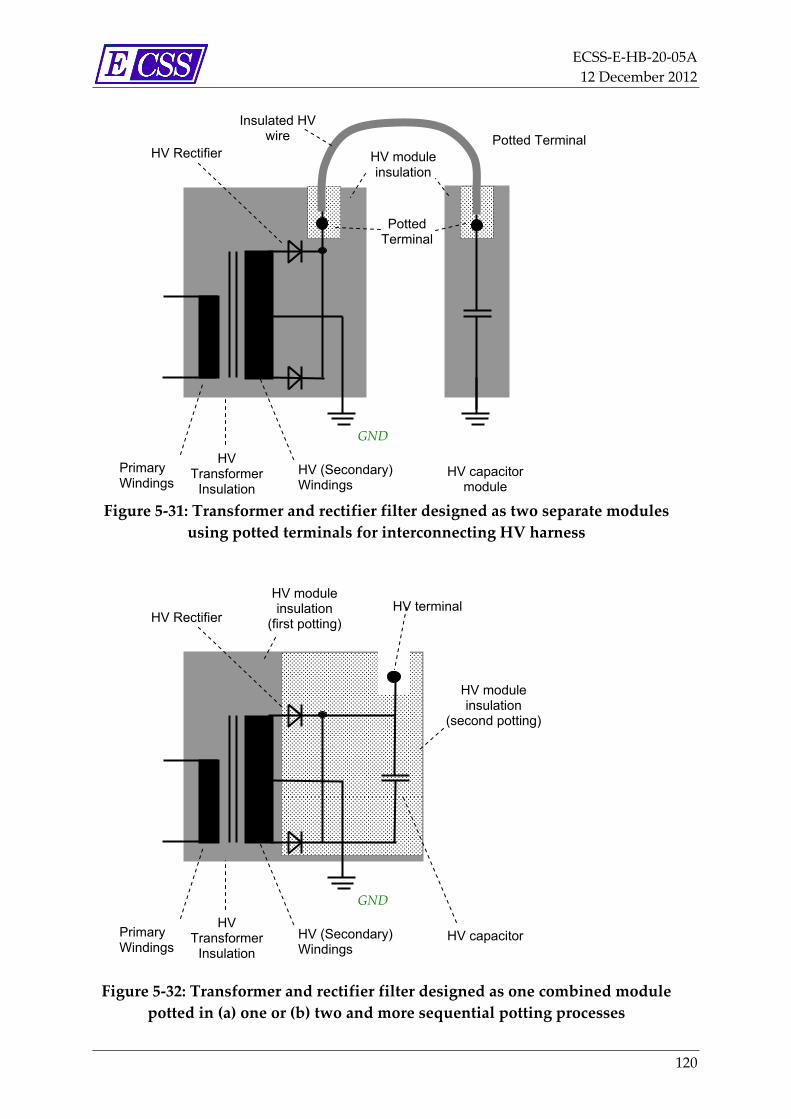
ECSS‐E‐HB‐20‐05A
12 December 2012
120
Figure 5‐31: Transformer and rectifier filter designed as two separate modules
using potted terminals for interconnecting HV harness
Figure 5‐32: Transformer and rectifier filter designed as one combined module
potted in (a) one or (b) two and more sequential potting processes
GND
Primary Windings
HV (Secondary)Windings
HV Transformer
Insulation HV capacitor
HV Rectifier HV terminal
HV module insulation
(first potting)
HV module insulation
(second potting)
GND
Primary Windings
HV (Secondary)Windings
HV Transformer
Insulation HV capacitor
module
HV Rectifier Potted Terminal
Insulated HV wire
HV module insulation
Potted Terminal
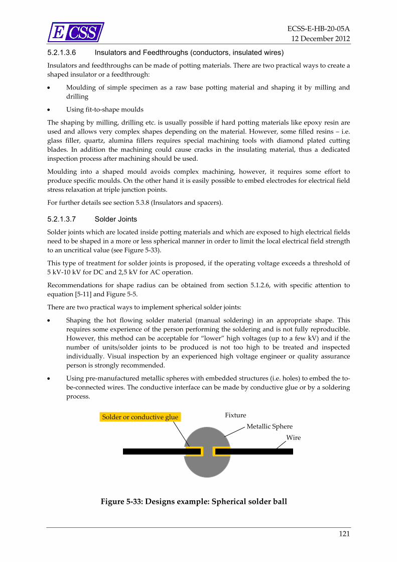
ECSS‐E‐HB‐20‐05A
12 December 2012
121
5.2.1.3.6 Insulators and Feedthroughs (conductors, insulated wires)
Insulators and feedthroughs can be made of potting materials. There are two practical ways to create a
shaped insulator or a feedthrough:
Moulding of simple specimen as a raw base potting material and shaping it by milling and
drilling
Using fit‐to‐shape moulds
The shaping by milling, drilling etc. is usually possible if hard potting materials like epoxy resin are
used and allows very complex shapes depending on the material. However, some filled resins – i.e.
glass filler, quartz, alumina fillers requires special machining tools with diamond plated cutting
blades. In addition the machining could cause cracks in the insulating material, thus a dedicated
inspection process after machining should be used.
Moulding into a shaped mould avoids complex machining, however, it requires some effort to
produce specific moulds. On the other hand it is easily possible to embed electrodes for electrical field
stress relaxation at triple junction points.
For further details see section 5.3.8 (Insulators and spacers).
5.2.1.3.7 Solder Joints
Solder joints which are located inside potting materials and which are exposed to high electrical fields
need to be shaped in a more or less spherical manner in order to limit the local electrical field strength
to an uncritical value (see Figure 5‐33).
This type of treatment for solder joints is proposed, if the operating voltage exceeds a threshold of
5 kV‐10 kV for DC and 2,5 kV for AC operation.
Recommendations for shape radius can be obtained from section 5.1.2.6, with specific attention to
equation [5‐11] and Figure 5‐5.
There are two practical ways to implement spherical solder joints:
Shaping the hot flowing solder material (manual soldering) in an appropriate shape. This
requires some experience of the person performing the soldering and is not fully reproducible.
However, this method can be acceptable for “lower” high voltages (up to a few kV) and if the
number of units/solder joints to be produced is not too high to be treated and inspected
individually. Visual inspection by an experienced high voltage engineer or quality assurance
person is strongly recommended.
Using pre‐manufactured metallic spheres with embedded structures (i.e. holes) to embed the to‐
be‐connected wires. The conductive interface can be made by conductive glue or by a soldering
process.
Figure 5‐33: Designs example: Spherical solder ball
Wire
Fixture
Metallic Sphere
Solder or conductive glue
ECSS‐E‐HB‐20‐05A
12 December 2012
122
5.2.1.4 Potting Process
For the production of potted high voltage modules a well defined and suitable potting process is the
key factor for providing a high performance and long‐life electrical insulation.
A major encapsulation problem (to be avoided) is the occurrence of cracks, voids, delamination and
particles in the material. In these areas the presence of strong voltage gradients leads to inception of
partial discharges and reduces the lifetime of the insulation. By taking care on the selection of an
encapsulant and of the related processing technique the problem can be minimized. A substantial
aspect of this technique is vacuum degassing of the encapsulant material before mixing, then mixing
and pouring in vacuum.
Although there are various possible processes depending on the material, for a high quality potting
process it is proposed to involve the following process steps:
1. Outgassing of potting material constituents
2. Mixing (if two or more component resins or fillers are used)
3. Warming up of resin mixture (if hot curing resin is used)
4. Pre‐heating of moulds (if the process requires high temperature and especially if metal
moulds are used)
5. Outgassing of moulds (if the process requires high temperature)
6. Casting under vacuum (preferred)
7. Casting under ambient pressure (not preferred)
8. Pressurizing to ambient
9. Pressurized curing (Autoclave)
10. Applying a temperature profile curing (stand‐alone or in combination with pressurized
curing).
It is highlighted, that a high quality potting process has to ensure, that within the steps 1‐6 the
vacuum environment is always present and is never interrupted (by pressurization) in this process
chain.
In order to achieve better mixing results, the potting components are warmed up before mixing. The
process steps could be the following:
Warming up and outgassing of potting material constituents
Mixing
Warming up of resin mixture.
After filling up the mould with resin, the vacuum can be removed (step 8) and the applied ambient
pressure squeezes the remaining gas bubbles enclosed in the still low viscose resin and can possibly
go into dilution. Applying additional high pressure is promoting this effect (step 9) – thus performing
the curing process in high pressure chamber (step 9), which is a further advantage.
Applying a thermal profile (step 10) is useful, especially if the curing takes place under elevated
temperature. At the end of the curing process it can be beneficial to stay for hours at elevated
temperature level before reducing the temperature stepwise.
Casting under ambient (step 7 instead of step 6) is not recommended, but can be unavoidable
depending on the selected potting material or due to restrictions of the circuitry/items to be potted. If
the casting is performed under ambient, it should be ensured, that the pre‐processing (steps 1‐4) are
performed in vacuum.
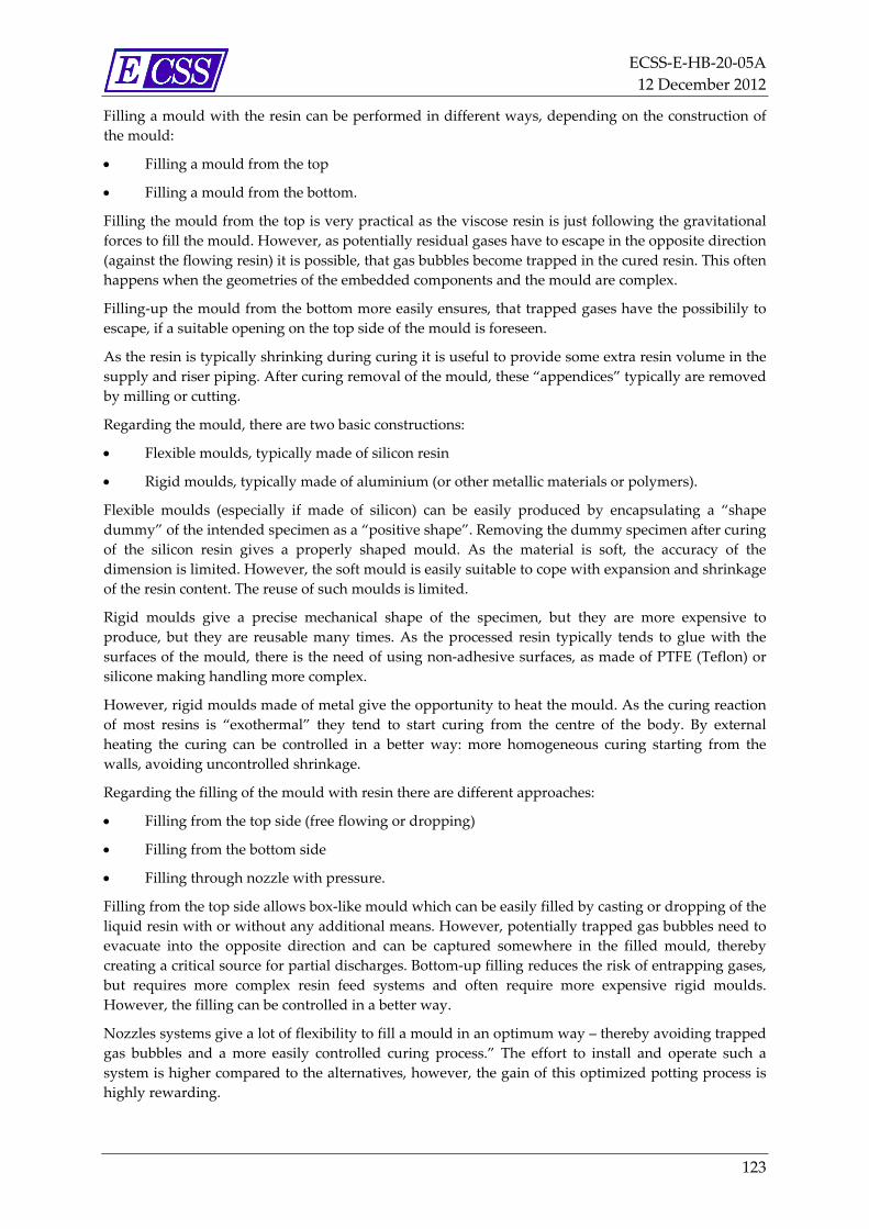
ECSS‐E‐HB‐20‐05A
12 December 2012
123
Filling a mould with the resin can be performed in different ways, depending on the construction of
the mould:
Filling a mould from the top
Filling a mould from the bottom.
Filling the mould from the top is very practical as the viscose resin is just following the gravitational
forces to fill the mould. However, as potentially residual gases have to escape in the opposite direction
(against the flowing resin) it is possible, that gas bubbles become trapped in the cured resin. This often
happens when the geometries of the embedded components and the mould are complex.
Filling‐up the mould from the bottom more easily ensures, that trapped gases have the possibilily to
escape, if a suitable opening on the top side of the mould is foreseen.
As the resin is typically shrinking during curing it is useful to provide some extra resin volume in the
supply and riser piping. After curing removal of the mould, these “appendices” typically are removed
by milling or cutting.
Regarding the mould, there are two basic constructions:
Flexible moulds, typically made of silicon resin
Rigid moulds, typically made of aluminium (or other metallic materials or polymers).
Flexible moulds (especially if made of silicon) can be easily produced by encapsulating a “shape
dummy” of the intended specimen as a “positive shape”. Removing the dummy specimen after curing
of the silicon resin gives a properly shaped mould. As the material is soft, the accuracy of the
dimension is limited. However, the soft mould is easily suitable to cope with expansion and shrinkage
of the resin content. The reuse of such moulds is limited.
Rigid moulds give a precise mechanical shape of the specimen, but they are more expensive to
produce, but they are reusable many times. As the processed resin typically tends to glue with the
surfaces of the mould, there is the need of using non‐adhesive surfaces, as made of PTFE (Teflon) or
silicone making handling more complex.
However, rigid moulds made of metal give the opportunity to heat the mould. As the curing reaction
of most resins is “exothermal” they tend to start curing from the centre of the body. By external
heating the curing can be controlled in a better way: more homogeneous curing starting from the
walls, avoiding uncontrolled shrinkage.
Regarding the filling of the mould with resin there are different approaches:
Filling from the top side (free flowing or dropping)
Filling from the bottom side
Filling through nozzle with pressure.
Filling from the top side allows box‐like mould which can be easily filled by casting or dropping of the
liquid resin with or without any additional means. However, potentially trapped gas bubbles need to
evacuate into the opposite direction and can be captured somewhere in the filled mould, thereby
creating a critical source for partial discharges. Bottom‐up filling reduces the risk of entrapping gases,
but requires more complex resin feed systems and often require more expensive rigid moulds.
However, the filling can be controlled in a better way.
Nozzles systems give a lot of flexibility to fill a mould in an optimum way – thereby avoiding trapped
gas bubbles and a more easily controlled curing process.” The effort to install and operate such a
system is higher compared to the alternatives, however, the gain of this optimized potting process is
highly rewarding.
ECSS‐E‐HB‐20‐05A
12 December 2012
124
For some resins it is possible to perform more than one sequential potting step, for example: first to
pot and to cure one part of the assembly and afterwards to pot and cure another section of the
assembly. With many epoxy resins as well as with polyurethanes and combinations of both, this is
feasible. Difficulties can be expected if silicone resins are used, as the surfaces can have some
difficulties in gluing together.
There are numerous effects and problems to maintain under control for a potting process, some of
these are listed in the following:
Sedimentation of fillers
Gas bubbles (in general)
Gas bubbles cause by encapsulated components (chemical reaction with surface and materials,
i.e. especially yarns, tapes and glues)
Delamination due to shrinkages caused by thermal effects or due to mass loss during the curing
process
Cracks due to shrinkage
Embedding of harnesses presents a risk, where a stranded wire surrounded by insulation, can
contain significant amounts of trapped gas, which can slowly escape during the curing process
as gas bubbles
Multiple material moulding has to handle different expansion cycles and coefficients causing
mechanical stress (cracks, delamination) and needs to ensure a good interface between
materials (adhesion).
In many case a partial discharge test is performed to characterize the quality and integrity of the
potted insulation. It is proposed to check the design of a potted assembly for the suitability of being
tested against partial discharges. Especially in complex assemblies with grounded structures the
partial discharge test configuration is not fully identical to the intended operational configurations. In
such cases the insulation can be modified to fit to the test scenario as well as to the operational
scenario. An example is shown in Figure 5‐34.
Figure 5‐34: Fitting a potted assembly to partial discharge testing (Example of a
potted transformer winding)
A) Sharp-edged non/isolated ground structure connectedto HV windings can cause problems for PD test
HV Terminal
Ground
HV Windings
B) Symmetrical high voltage connection, both sides(including the lead to ground) are fully isolatedallowing full partial discharge testing of the pottingmaterial
HV Terminal
HV Windings
Ground

ECSS‐E‐HB‐20‐05A
12 December 2012
125
5.2.1.5 Life Limiting Factors
The major life limiting factors for potted assemblies are:
thermo‐cycling
high temperature
low temperature
radiation (cosmic and ultraviolet)
humidity.
Thermal cycling is a most important ageing factor especially for hard potting materials as the thermo‐
mechanical stresses can result in cracking and delamination after a while.
High temperature is critical in general, as the chemical destruction and electrical ageing progresses
faster than at lower temperatures.
Low temperature increases the brittleness of most potting materials resulting in cracking.
Radiation in the ultraviolet range or hard cosmic radiation can result in destruction of polymeric
chains, making the material more brittle with time. Cosmic radiation can cause space charges inside of
the material increasing local electrical stress.
Humidity as an environmental factor on ground can increase the electrical loss factor.
5.2.1.6 Thermal management
Often dissipating components are embedded in the potted insulation. As the thermal conductivity of
the potting material is low compared to metallic materials, the draining of heat is often a problematic
issue. The maximum operating temperatures of these insulation materials is typically between 80 °C
and 120 °C – depending on the limitations given by the stress‐lifetime curve.
Basically there are two means of increasing the heat drain capability of a potted module (see Figure 5‐35).
Using a high conductive filler
Embedding a high conductive drain structure made of metal (copper, aluminium) or ceramic.
Figure 5‐35: Examples for thermal drains embedded in potted modules
A) Heat drain by embedded metallic structure – here rod with rounded shape to control electrical field
Baseplate
Metallic rod as a heat sink
Ground
Heat dissipating component
Baseplate
Ceramic structure as a heat sink
Ground
Heat dissipating component
B) Heat drain by embedded ceramic structure – here providing insulation function
ECSS‐E‐HB‐20‐05A
12 December 2012
126
High conductive fillers are quartz (glass), boron nitride and alumina. However, to achieve good
results the percentage of fillers, the grain size of fillers and the potting process need to be very well
matched. Highly optimized potting materials for high voltage insulation can achieve thermal
conductivity in order of 1 W/m K.
Thermal drain structures made of metal or ceramic can help to improve the heat flux from high
dissipating embedded components. If metal structures are used, special care should be taken to avoid
implications with high electrical field strength, as the embedded metal structure reduces the
insulation distance to high voltage conductors. The use of ceramic structures can increase thermal
conductivity as well, however, not as well as a metallic structure. However, the ceramic does not
weaken the insulation so much. Of course, there is an impact, that the embedded ceramic modifies the
electrical field distribution; this provides a weak surface between the ceramics and potting material
interface.
This should be carefully matched with the thermal expansion of the embedded material.
5.2.1.7 Thermo-mechanical matching
In a perfect case, the thermal expansion coefficient of the embedding potting material is equally
matched to the embedded component inside the potting material. For embedding of electronic
components this is difficult to achieve, as substrate materials are typically made of ceramics and as
conductor materials are typically metallic or silicon, both have lower thermal expansion coefficients
than typical potting materials. Using fillers for the potting material can help to reduce the mismatch in
coefficients. Suitable fillers are quartz (glass), boron nitride and alumina. Often it is advantageous
using a process which cures at higher temperatures than the maximum operating temperature of the
potted module, as to allow shrinking of the insulation material onto the embedded components. This
can help to prevent delamination in the interface; however, pressure forces generally need to be
controlled to avoid cracking.
It is highlighted, that one is careful when curing of potted material is made with temperature sensitive
components embedded in the potting. Not only “active” components are at stake here, even “passive”
components / materials can be negatively affected if the curing temperature is too high.
5.2.1.8 Other aspects
Special attention regarding design should be addressed to the following points:
Control of surface charging – see section 5.1.12
Control of interferences – see section 5.1.11
Control of corona effects – see section 5.1.7
5.2.1.9 Long-term stability
The long‐term stability of potted high voltage insulation is excellent under the condition that they are
properly designed
using a high quality materials and processes.
Lifetimes of 15‐20 years and longer can be assumed as a standard.
ECSS‐E‐HB‐20‐05A
12 December 2012
127
5.2.1.10 Reparability
Potted insulations are difficult to repair – in flight anyway there is no possibility, on ground only in
very exceptional cases, for example when an easily removable soft potting material is used, which
then can be mechanically removed and replaced.
5.2.1.11 References of potted insulations
For space missions solid insulations are “state of the art” for EPC´s in communication and radar
applications, worldwide they have a heritage of more than 30 years.
5.2.1.12 Costs
The production of potted insulations require a well established process for obtaining a high quality
insulation, a facility that allows for the preparation, mixing and moulding under vacuum conditions is
beneficial. Furthermore, specially designed tools (moulds) are used. Therefore non‐recurring costs for
potted insulations are typically high, but some benefits can be achieved for non‐recurring cost in serial
production.
5.2.1.13 Recommendation for use
Potted insulation is the preferred solution for any kind of spaceborne high voltage equipment up to a
certain volume/size. Limitations when the moulded item gets too bulky – exceeding for example a few
kilogram of mass or the operating temperatures at the insulation hot spot exceed the range of 80 °C ‐
110 °C. Potted insulation can be of lower preference if the application uses another insulation concept
(i.e. liquid, gas, vacuum).
5.2.2 Solid insulation: others
5.2.2.1 General
5.2.2.1.1 Polymers (other)
In addition to the potting materials (see section 5.2.1) the following polymers are used in some
applications:
PMMA ‐ Polymethylmetacrylat (Trademarks: “Acryl”)
used for spacers and insulators
PEEK ‐Polyetheretherketone
used for spacers
PI – Polyimide
used for cable insulation up to 600 V (currently)
rarely used for higher voltages on cables,
also used for high voltage PCB’s
PTFE, FTE – Polytretrafluorethylene
used for cable insulation and spacers
PE – Polyethylene
used for cable insulation
ECSS‐E‐HB‐20‐05A
12 December 2012
128
All these materials are delivered as pre‐manufactured raw materials and shaped by milling and
cutting. They are typically used as spacers, or feedthroughs, and are not suitable for full encapsulation
like potting materials.
For special considerations regarding pre‐manufactured raw materials see section 5.2.2.1.8 “General
aspects of raw insulation materials”.
5.2.2.1.2 Ceramics
While porcelain is the standard ceramics for terrestrial applications, for space applications typically
ceramic materials based on Alumina (Aluminium Oxides) are used.
Some of these ceramic materials are “soft’ enough, that pre‐manufactured raw materials (like rods and
boards) can be cut and milled to achieve the required shape. Other ceramics with “hard” structure
need to be shaped before the sintering process and can furthermore be slightly trimmed afterward by
especially hardened tools (diamond). The sintering process is typically performed on site of a
specialized ceramics supplier. In some cases, ceramic adhesives are available, which can be processed
by the users themselves.
For special considerations regarding pre‐manufactured raw materials see section 5.2.2.1.8 “General
aspects of raw insulation materials”.
As ceramic materials are very brittle, cracking of the raw material and of the manufactured insulator is
a typical problem. Inspections and proper mechanical interfacing is strongly recommended.
5.2.2.1.3 Glass
Glass is sometimes used as packaging for semiconductors and of tubes. As it needs to be molten and
shaped at high temperatures it is used for a very limited range of applications.
5.2.2.1.4 Insulation by dispensing, spraying, or dipping
For low mass insulation it appears to be very attractive to dispense insulation in thin layers on high
voltage assemblies, especially on PCB structures. The problem areas for such kind of insulations are:
Ensuring a defined (minimum) thickness of all surfaces including at sharp edges and “hidden”
areas.
Avoiding inclusion of voids.
Suppressing surface charging effect of the outer insulation surface and avoiding partial discharges
/ corona if the assembly is operated under AC in gaseous or in low pressure environment.
In practice, the key problem is to ensure a defined minimum thickness of the insulation as the
processed material needs to be ‘liquid” enough to be dispensed, sprayed or dipped, but then has to
adhere immediately to cure at the right place. Sharp edges and corners increase theses difficulties. The
difference from potted insulation, where the dimension of the insulation is clearly defined by the
filling of the mould, here a method is used to verify the required thickness. This is more important at
higher voltages (above a few kV), where the insulation thickness needs to be in the range over a few
tenths of a millimetre or millimetres.
5.2.2.1.5 Sintered insulation
Polyimide (Trademarks of polyimide films include Apical, Kapton, UPILEX, VTEC PI, Norton TH and
Kaptrex and polyimide parts and shapes include P84 NT, VTEC PI, Meldin, Vespel and Plavis) and
PTFE (Polytetrafluoroethylene, Trademark: Teflon) are typically processed by sintering at suppliers
premises. One way of making such material is in the format of rods and boards to be machine later by
the user. Another method is used by the manufacturers of specific cables, where tapes of such a
material are wound around a conductor. The resulting multi‐layer assembly is sintered at high
ECSS‐E‐HB‐20‐05A
12 December 2012
129
temperature to form a mostly homogeneous insulation. More information about high voltage cables is
given in section 5.3.5.
5.2.2.1.6 Chemical vapor deposited polymers insulation
An interesting method is the vapour deposition of a polymer on a surface forming thin high voltage
insulation. Such a method is practically given by vapor deposited poly(p‐xylylene) polymers mostly
used under the trademark Parylene. In the military/aerospace market there are two variants mostly
used, the Parylene C and the Parylene HT. Due to the vapor deposition, a pinhole free layer can be
established. Critical is the stability of the material, especially with respect to ultraviolet irradiation,
where only the HT variant seems to be significantly less sensitive.
The result is a very low mass insulation; however, the problem areas for such kind of insulations are the
same as for Insulation by dispensing, spraying, or dipping (see section 5.2.2.1.4). The use of the process
can be subject to restrictions (for HT) and can be only possible to be performed at supplier’s premises.
5.2.2.1.7 Powder insulation
In order to take advantage of a good heat transfer from highly dissipating electronic parts is filling a
box containing the electronic circuitry with a ceramic power, like boron nitride or alumina. The
powder should be a well composed mixture of particles with different particle sizes, and the filling
has to combine a compression process with high forces and vibration to ensure a high degree of filling.
In combination with space vacuum and after appropriate outgassing time the powder insulation can
grant suitable high voltage withstanding capability. A risk with the inclusion of air is if the outgassing
is not sufficient, resulting in partial discharges and degradation.
A reference is made to:
F. Boer, BN100 filler technology, ARTHE Engineering Solutions S.R.L., 2004,
ESA Contract 18697/04 and European Patent Application EP0993238
5.2.2.1.8 General aspects of raw insulation materials
In case that high voltage insulation is made on the basis of pre‐manufactured raw material, a high
quality of high voltage insulation can be ensured only under the following conditions:
the material is suitable for high voltage insulation
the production process ensures that the material does not contain voids, holes, included
contamination and equal distribution of dielectric properties.
the raw material is subject of a dedicated incoming inspection
the machining and use of the raw materials is performed by a process which does not result in
cracking and delamination of the material, or changes the electrical insulation properties.
The use of the material respect the rules described in section 5.1 “Basic design principles” –
especially avoiding critical electrical field stresses.
5.2.3 Gaseous insulation
5.2.3.1 General
The design of gaseous insulations is comfortable in so far as there is no significant electrical ageing of
the gas and the insulation strengths is clearly predictable. Degradation is mostly related to pressure
loss (gas leakage) of pressurized containments or chemical degradation.
ECSS‐E‐HB‐20‐05A
12 December 2012
130
The design cases are driven by the boundary condition of the gases. An overview of insulation
properties of typical gases is given in Table 4‐2. Either the gas is a natural environment, as it is for
ambient air on earth or in manned space vehicles, or is a selected gas in a pressurized containment.
Natural gas environments:
Air
Carbondioxide, Methan on some planets and moons
Often used artificial gas environments:
Nitrogen (often selected for insulation purposes)
Carbondioxide (e.g. lasers)
Inert Gases: Helium, Xenon, Neon (e.g. for laser, electric propulsion)
SF6 Sulfurhexafluoride (high performance insulation gas)
The electric strength of a gaseous insulation depends significantly on the pressure. The breakdown
voltage of a uniform‐field gap in a gaseous environment can be expressed as a function of gas
pressure times the gap length. This characteristic is known as the Paschenʹs law and expressed in the
Paschen curve (see Figure 4‐7 in section 4.3.4). The law of the breakdown voltage Ubd can be written in
the form:
)( pdfUbd
where p is the gas density and d the distance between parallel plates. The pressure corresponding to
minimum breakdown strength depends on the spacing of the electrodes. Detailed curves and tables
are given in section 4.3.4.)
When the pressure is increased to values greater than two atmospheres, or when the field exceeds
100 kV/cm, Paschenʹs law is no longer satisfied. The breakdown strength Ed can be estimated by the
following equation
a
d
d
p
p
pE
pE
00 )(
)(
[5‐19]
where:
)( pEd Breakdown field strengths at pressure p
)( 0pEd Breakdown field strengths at reference pressure p0
a Exponent typically between 0,6 .. 0,8
In non‐uniform electrical fields the breakdown voltage depends on the non‐homogeneity and the
polarity of the gap. A characteristic value is the utilization factor which is defined as the ratio of the
average to the maximum gradient across the gap. High values of the utilization factor cause a low
flashover voltage.
Gaps with an unsymmetrical non‐uniform field of positive polarity (at the electrode where the higher
field strength is present) have a lower breakdown voltage as such with negative polarity. Indeed
negative unsymmetrical gaps show partial discharge at lower voltages but the total breakdown occurs
at much higher values (for more details see section 5.1.2).
A list of properties of selected gases can be found in Table 4‐2. Despite of the typical air environment
or nitrogen, most interesting are gases like the fluorocarbons and SF6. They have outer rings deficient
of one or two electrons. These molecules are able to capture free electrons forming heavy and
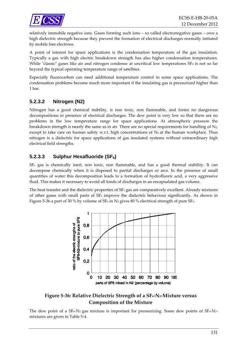
ECSS‐E‐HB‐20‐05A
12 December 2012
131
relatively immobile negative ions. Gases forming such ions – so called electronegative gases – owe a
high dielectric strength because they prevent the formation of electrical discharges normally initiated
by mobile free electrons.
A point of interest for space applications is the condensation temperature of the gas insulation.
Typically a gas with high electric breakdown strength has also higher condensation temperatures.
While ʺclassicʺ gases like air and nitrogen condense at uncritical low temperatures SF6 is not so far
beyond the typical operating temperature range of satellites.
Especially fluorocarbon can need additional temperature control in some space applications. The
condensation problems become much more important if the insulating gas is pressurized higher than
1 bar.
5.2.3.2 Nitrogen (N2)
Nitrogen has a good chemical stability, is non toxic, non flammable, and forms no dangerous
decompositions in presence of electrical discharges. The dew point is very low so that there are no
problems in the low temperature range for space applications. At atmospheric pressure the
breakdown strength is nearly the same as in air. There are no special requirements for handling of N2,
except to take care on human safety w.r.t. high concentrations of N2 at the human workplace. Thus
nitrogen is a dielectric for space applications of gas insulated systems without extraordinary high
electrical field strengths.
5.2.3.3 Sulphur Hexafluoride (SF6)
SF6 gas is chemically inert, non toxic, non flammable, and has a good thermal stability. It can
decompose chemically when it is disposed to partial discharges or arcs. In the presence of small
quantities of water this decomposition leads to a formation of hydrofluoric acid, a very aggressive
fluid. This makes it necessary to avoid all kinds of discharges in an encapsulated gas volume.
The heat transfer and the dielectric properties of SF6 gas are comparatively excellent. Already mixtures
of other gases with small parts of SF6 improve the dielectric behaviour significantly. As shown in
Figure 5‐36 a part of 30 % by volume of SF6 in N2 gives 80 % electrical strength of pure SF6.
Figure 5‐36: Relative Dielectric Strength of a SF6‐N2‐Mixture versus
Composition of the Mixture
The dew point of a SF6‐N2 gas mixture is important for pressurizing. Some dew points of SF6‐N2‐
mixtures are given in Table 5‐4.
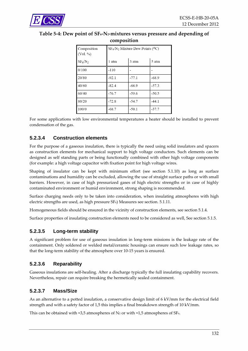
ECSS‐E‐HB‐20‐05A
12 December 2012
132
Table 5‐4: Dew point of SF6‐N2‐mixtures versus pressure and depending of
composition
For some applications with low environmental temperatures a heater should be installed to prevent
condensation of the gas.
5.2.3.4 Construction elements
For the purpose of a gaseous insulation, there is typically the need using solid insulators and spacers
as construction elements for mechanical support to high voltage conductors. Such elements can be
designed as self standing parts or being functionally combined with other high voltage components
(for example: a high voltage capacitor with fixation point for high voltage wires.
Shaping of insulator can be kept with minimum effort (see section 5.1.10) as long as surface
contaminations and humidity can be excluded, allowing the use of straight surface paths or with small
barriers. However, in case of high pressurized gases of high electric strengths or in case of highly
contaminated environment or humid environment, strong shaping is recommended.
Surface charging needs only to be taken into consideration, when insulating atmospheres with high
electric strengths are used, as high pressure SF6) Measures see section. 5.1.11.
Homogeneous fields should be ensured in the vicinity of construction elements, see section 5.1.4.
Surface properties of insulating construction elements need to be considered as well, See section 5.1.5.
5.2.3.5 Long-term stability
A significant problem for use of gaseous insulation in long‐term missions is the leakage rate of the
containment. Only soldered or welded metal/ceramic housings can ensure such low leakage rates, so
that the long‐term stability of the atmosphere over 10‐15 years is ensured.
5.2.3.6 Reparability
Gaseous insulations are self‐healing. After a discharge typically the full insulating capability recovers.
Nevertheless, repair can require breaking the hermetically sealed containment.
5.2.3.7 Mass/Size
As an alternative to a potted insulation, a conservative design limit of 6 kV/mm for the electrical field
strength and with a safety factor of 1,5 this implies a final breakdown strength of 10 kV/mm.
This can be obtained with ≈3,5 atmospheres of N2 or with ≈1,5 atmospheres of SF6.
ECSS‐E‐HB‐20‐05A
12 December 2012
133
In this case, the EPC size would be in the same order of magnitude as conventional EPC’s with potted
HV circuits, but requiring a pressure load.
5.2.3.8 References of Gaseous Insulations
In space missions, gaseous insulations have been used for:
XSAR / SRTM HPA
This X‐Band radar was flown on a common DLR/NASA radar earth observation mission (1993/1998).
The HPA was built by Dornier System (now EADS Astrium) and is based on the ERS‐design (vacuum
insulated design, see section 5.2.5.10). Maximum high voltage is 17 kV.
Since the mission was scheduled on several US Space Shuttle flights, the High Power Amplifier (HPA)
with the high voltage power conditions has been kept in a sealed container under 1 atmosphere of N2.
The lid of this assembly is equipped with a metal sealing and is removable. Operation was in the open
payload bay of the US space shuttle – mission time was a few ten days in space environment.
Communication TWTA
Some approaches are known from the FIAR company (now Selex Galileo) in the 1980´s to build EPC´s
for communication TWT´s with voltage up to 6 kV in hermetically sealed containments (welded lids)
pressurized with SF6. These EPCs have been flown on OTS and EUTELSAT I (former ECS) satellites.
A pair of TWTA’s has been flown on the ESA/NASA mission Ulysses with a flight to Jupiter being
operational from 1991 till 2008.
FSL BDPU
FSL BDPU was an scientific experiment flown on US Space Shuttle in a manned ESA/NASA mission
(1998), providing a fluid science experiment. An alternating high voltage of 20 kVpeak (frequency 0
kHz ‐ 10 kHz) was isolated in an SF6 filled containment (1,1 hPa pressure). The supplier was Dornier
Satellite Systems (now Astrium).
FASES GeoFlow
FASES GeoFlow is a scientific experiment planned flown on the International Space Station (as part of
the European Columbus module), providing a fluid science experiment. An alternating high voltage
of 10 kV‐rms. (frequency 1 kHz ‐ 10 kHz) is isolated in an SF6 filled containment (1,1 hPa pressure).
The supplier is EADS Space (now Astrium).
5.2.3.9 Costs
Compared with conventional EPC´s with potted HV, there is some cost saving with the absence of
complex potting process. Nevertheless, it can be difficult, to replace all potted parts by “open” parts
(difficult for transformer windings), so partial potting is still necessary. The need of a hermetically
sealed house can at least compensate the cost saving in potting.
5.2.3.10 Recommendation for use
The hermetically sealed containment necessary for the gaseous insulations is a risk for long‐term
missions. The cost and mass savings by reduction of EPC potting is expected to be (over‐)
compensated by penalties of the housing. Therefore gaseous insulation appears suitable only for some
“niche” applications in short‐term / mid‐term missions or manned space flight.
ECSS‐E‐HB‐20‐05A
12 December 2012
134
5.2.4 Liquid insulation (Oil)
5.2.4.1 General
Liquids insulations are self healing – with some restrictions. After a temporary overvoltage the
affected area of a breakdown path is immediately reinsulated by fluid flow, nevertheless often some
degradation remains. Often, liquid dielectrics are used in conjunction with solid insulations such as
parts, films, and composite materials. By eliminating enclosed gases, the strength of a liquid insulation
system is improved significantly.
The operating temperature of a liquid dielectric affects its life and stability. A pure liquid, in the
absence of water or oxygen, should be very stable at rather high temperatures. With increased
temperatures, fluid viscosity decreases and the higher mobility of the ions implies increased
conduction. Refining techniques, additives, and blending of liquids are used for thermal upgrades.
Moisture reduces the reliability of liquid insulation. Water usually decreases dielectric strength and
increases dielectric loss. Polar contaminants dissolved in oil give moisture its greatest degradation
effect on dielectric strength.
The effect of gas absorption and liberation should be considered for long‐term, successful operation.
Changes in pressure can make dissolved gases evolve from a liquid. Also, temperature affects the
solubility of gas, so heating can cause dissolved gas to evolve from the liquid. Partial discharges start
in the evolved gas bubbles, leading to eventual breakdown.
Especially for space borne liquid insulated systems it should be taken care that the liquid is kept
pressurized so that gas bubbles do not form.
In selecting a liquid dielectric, its properties should be evaluated in relation to the application. The
most important are dielectric strength, dielectric constant and conductivity, flammability, viscosity,
thermal stability, purity, flash point, chemical stability, and ‐ very important ‐ compatibility with other
materials of construction and the local atmosphere.
On ground, mineral oils are most commonly used for high voltage equipment insulation. Silicones are
necessary for specialized applications with fire resistance requirements and high operating
temperatures. However, the use of oil‐based insulation is a strong penalty for satellite level testing as
there is a risk of severe contamination of the test chamber and of the satellite equipments in case of
leakage, especially when thermal vacuum testing is performed.
5.2.4.2 Long-term stability
Liquid insulation can degrade by chemical decomposition, partial discharges, dissolved gases and
increased water content. Decomposition due to radiation is possible, too. As there is no knowledge
about space borne liquid insulated high voltage equipment it is therefore not possible to give a clear
indication of long‐term stability. As a global indication, liquid insulated high voltage systems are
suitable for stable operation from a few weeks to a couple of years, without maintenance therefore
being more life limited than solid insulations.
5.2.4.3 Reparability
Due to a limited self‐healing capability, a pure liquid insulation recovers its strength after a
breakdown; however, degradation is likely, especially after repeated discharges. If after a breakdown
the insulation is degraded, it is possible to replace (refill) the liquid (on ground). In composite
liquid/solid insulations (impregnated foils) the reparability is much more limited, as the solid
insulation parts can be damaged as well and those do not recover.
ECSS‐E‐HB‐20‐05A
12 December 2012
135
5.2.4.4 References of Liquid Insulations
The only available reference is the scientific experiment FASES GeoFlow been flown on the ESA
mission onboard the ISS (two flight missions in 2008 and 2010). A part of the experiment is isolated by
a liquid. Parameters are a high voltage of 10kV‐rms. (frequency 1‐10 kHz). Operation was short‐term a
couple of days.
5.2.4.5 Costs
The costs for liquid insulated system are in the mid range. There are basic costs associated with the
need of a sealed containment, whereas the overall design of the high voltage elements is simpler and
therefore at lower costs, compared with solid insulation.
5.2.4.6 Recommendation for use
Due to the complexity given by the use of a hermetically sealed and pressurized assembly, the use
should be limited to experimental equipment and large high power equipment in cases where potted
insulation are critical due to bulk effects.
5.2.5 Space vacuum insulation
5.2.5.1 General
The natural environment of space, the vacuum, appears to be ideally suited for high voltage
insulation. The “pure” high vacuum is an excellent insulator. Using the natural vacuum of space
certainly can aid to mass savings, since solids and liquid dielectrics are minimized. In addition the
problem of providing a reliably sealed containment for gas or liquid is avoided. Conduction currents
in vacuum are very low as long as no pre‐breakdown effects appear (see section 4.3.2.5).
There are some important facts to consider for vacuum insulation design:
It is very difficult to achieve a vacuum insulation, which is completely free of discharges and
sporadic breakdown.
Therefore a vacuum insulated design and the surrounding electrical circuitry needs to be
tolerant and hardened to survive sporadic flashovers, for example by introduction of:
discharge energy or current limitations to prevent overload of the affected electrical
circuit
suitable EMC design to avoid disturbances in case of breakdown
shields to prevent discharge to inject energy into sensitive electric lines
overvoltage suppression devices to prevent mitigation of failures into sensitive parts of
the electronic circuit
The breakdown strength of vacuum is drastically lowered, when insulating surfaces are present
in an area of high electrical field strengths. The reduction is difficult to predict, as it depends on
surface properties, including surface layers, absorbed gases, micro particles, properties w.r.t
electrical charging (secondary electron emission coefficient of insulation, field emission
behaviour of electrical conductors, electrical surface conductivity), temperature, residual gas
pressure, shapes and aspects of the triple‐junction zone.
The sensitivity to such “degrading” effects depends significantly on the voltage as in the free
path the energy of accelerated electrons is linearly increasing with the voltage. Practically one
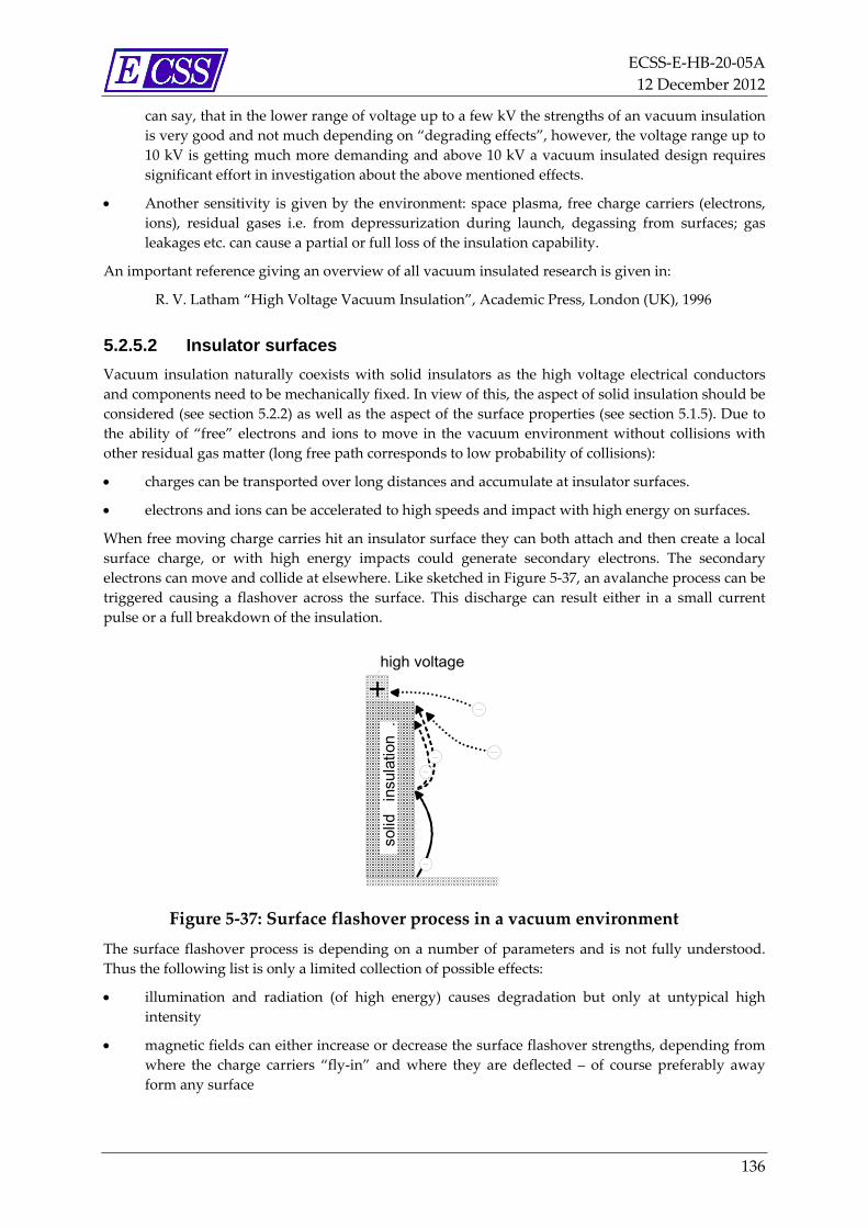
ECSS‐E‐HB‐20‐05A
12 December 2012
136
can say, that in the lower range of voltage up to a few kV the strengths of an vacuum insulation
is very good and not much depending on “degrading effects”, however, the voltage range up to
10 kV is getting much more demanding and above 10 kV a vacuum insulated design requires
significant effort in investigation about the above mentioned effects.
Another sensitivity is given by the environment: space plasma, free charge carriers (electrons,
ions), residual gases i.e. from depressurization during launch, degassing from surfaces; gas
leakages etc. can cause a partial or full loss of the insulation capability.
An important reference giving an overview of all vacuum insulated research is given in:
R. V. Latham “High Voltage Vacuum Insulation”, Academic Press, London (UK), 1996
5.2.5.2 Insulator surfaces
Vacuum insulation naturally coexists with solid insulators as the high voltage electrical conductors
and components need to be mechanically fixed. In view of this, the aspect of solid insulation should be
considered (see section 5.2.2) as well as the aspect of the surface properties (see section 5.1.5). Due to
the ability of “free” electrons and ions to move in the vacuum environment without collisions with
other residual gas matter (long free path corresponds to low probability of collisions):
charges can be transported over long distances and accumulate at insulator surfaces.
electrons and ions can be accelerated to high speeds and impact with high energy on surfaces.
When free moving charge carries hit an insulator surface they can both attach and then create a local
surface charge, or with high energy impacts could generate secondary electrons. The secondary
electrons can move and collide at elsewhere. Like sketched in Figure 5‐37, an avalanche process can be
triggered causing a flashover across the surface. This discharge can result either in a small current
pulse or a full breakdown of the insulation.
sol
id
insu
latio
n .
high voltage
Figure 5‐37: Surface flashover process in a vacuum environment
The surface flashover process is depending on a number of parameters and is not fully understood.
Thus the following list is only a limited collection of possible effects:
illumination and radiation (of high energy) causes degradation but only at untypical high
intensity
magnetic fields can either increase or decrease the surface flashover strengths, depending from
where the charge carriers “fly‐in” and where they are deflected – of course preferably away
form any surface

ECSS‐E‐HB‐20‐05A
12 December 2012
137
surface treatment is important, but its effect is difficult to predict. Often however, it has been
observed that a specific surface roughness is advantageous in comparison to polished surfaces –
as long as the roughness is not too deep and associated with loose particles. Furthermore, a
slightly conductive surface is helpful to avoid surface charging, but is in practice, difficult to
establish as in the high ohmic domain, it is difficult to keep a low homogenous conductivity.
Sometimes a work‐around can be to install intermediate shields to control the electrical field
distribution and superimposing field distortions by surface charges (see implementation
example in Figure 5‐24).
the applied waveform can give some advantage for pulsed voltages in the μs‐range and less,
lowest strengths is typically obtained for AC voltages with ms sinus period and in most cases a
higher value for DC voltages.
geometry is an important driver as the inclination of the surface (surface angle) determines if a
surface is hit by electrons; in combination with material surface properties this determines
further the triggering of secondary electron avalanches. Some examples of shapes are shown in
Figure 5‐38. Typical results shown most critically for slightly negative cone angles θ,
presumably as the electrons can easily hit the surface and the avalanche can “slide” along it.
Good results are likely (but nor guaranteed) for cone angles θ in the order of 45 degree. Several
combinations of surface angles, materials and waveforms are presented in Table 5‐5.
triple‐junction zones are the possible emission sites in the “corner” between the solid insulator,
the vacuum and metal especially at the cathode: therefore it is important to reduce the electrical
field in this zone (i.e. Figure 5‐38: cylinders with inserts).
pre‐stress of a set‐up has an effect on the strengths, especially after a polarity change from a
negative to a positive voltage and vice versa a reduction of the breakdown strengths can appear
– most likely caused by the build‐up of space charges.
conditioning is a frequently found effect, meaning, that after a surface flashover has occurred,
subsequent flashovers happen at higher voltages – as long as the dumped energy does not
destroy the set‐up significantly.
the material has an impact on surface flashover strengths of insulators in vacuum – however,
results of studies are often contracting. Some important observations are: first, that
homogeneous materials tend to make better insulators, and second, that there is an inverse
relationship of voltage strength to the relative permittivity (epsilon) of the material. Most likely
materials with a higher permittivity tend to concentrate the field more in the triple‐junction
zone, which eases the emission of electrons and consequently weakens the insulation.
surface gases play a role, if they are easy to release – therefore the best is to release any surface
gases by baking out and/or sufficiently long exposure to a good vacuum environment.
a temperature increase lowers the breakdown strengths, typically
The Table 5‐6 summarizes some theoretical predictions to improve the electrical strengths of insulator
surface in vacuum in relation to practical measures.
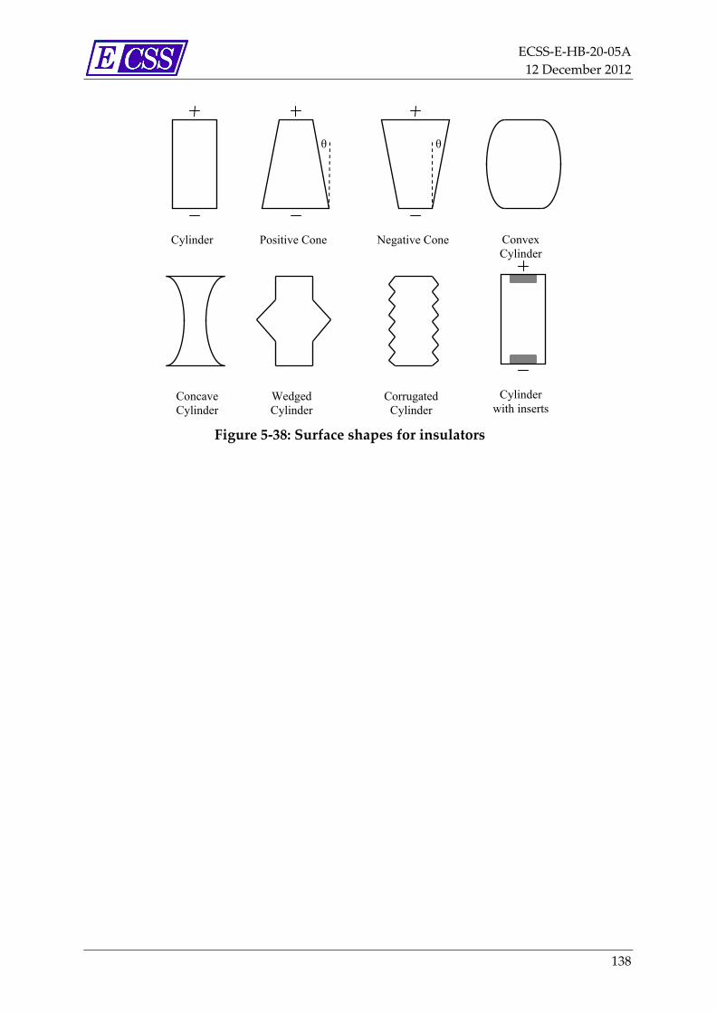
ECSS‐E‐HB‐20‐05A
12 December 2012
138
Figure 5‐38: Surface shapes for insulators
Cylinder Positive Cone Negative Cone
θ θ
Wedged Cylinder
Concave Cylinder
Corrugated Cylinder
Convex Cylinder
Cylinder with inserts
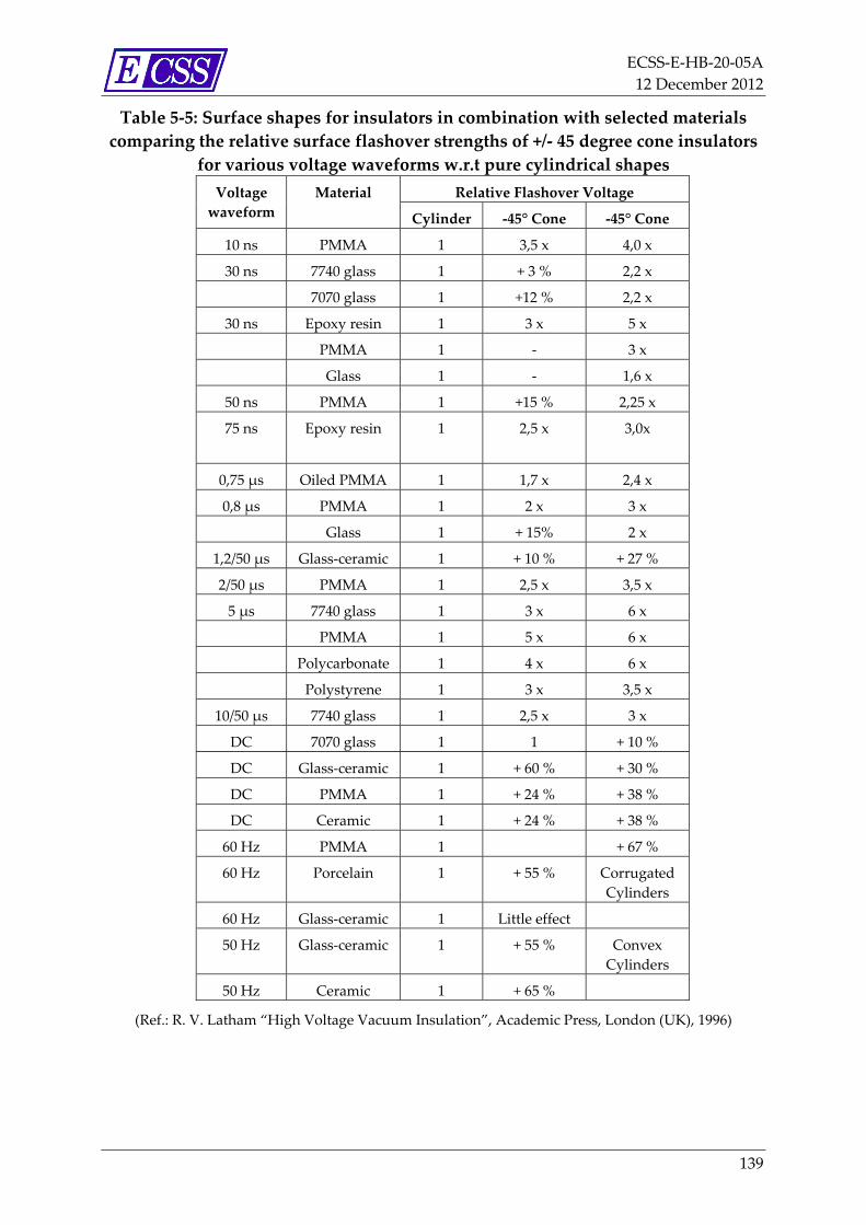
ECSS‐E‐HB‐20‐05A
12 December 2012
139
Table 5‐5: Surface shapes for insulators in combination with selected materials
comparing the relative surface flashover strengths of +/‐ 45 degree cone insulators
for various voltage waveforms w.r.t pure cylindrical shapes
Voltage
waveform
Material Relative Flashover Voltage
Cylinder ‐45° Cone ‐45° Cone
10 ns PMMA 1 3,5 x 4,0 x
30 ns 7740 glass 1 + 3 % 2,2 x
7070 glass 1 +12 % 2,2 x
30 ns Epoxy resin 1 3 x 5 x
PMMA 1 ‐ 3 x
Glass 1 ‐ 1,6 x
50 ns PMMA 1 +15 % 2,25 x
75 ns Epoxy resin
1 2,5 x 3,0x
0,75 μs Oiled PMMA 1 1,7 x 2,4 x
0,8 μs PMMA 1 2 x 3 x
Glass 1 + 15% 2 x
1,2/50 μs Glass‐ceramic 1 + 10 % + 27 %
2/50 μs PMMA 1 2,5 x 3,5 x
5 μs 7740 glass 1 3 x 6 x
PMMA 1 5 x 6 x
Polycarbonate 1 4 x 6 x
Polystyrene 1 3 x 3,5 x
10/50 μs 7740 glass 1 2,5 x 3 x
DC 7070 glass 1 1 + 10 %
DC Glass‐ceramic 1 + 60 % + 30 %
DC PMMA 1 + 24 % + 38 %
DC Ceramic 1 + 24 % + 38 %
60 Hz PMMA 1 + 67 %
60 Hz Porcelain 1 + 55 % Corrugated
Cylinders
60 Hz Glass‐ceramic 1 Little effect
50 Hz Glass‐ceramic 1 + 55 % Convex
Cylinders
50 Hz Ceramic 1 + 65 %
(Ref.: R. V. Latham “High Voltage Vacuum Insulation”, Academic Press, London (UK), 1996)
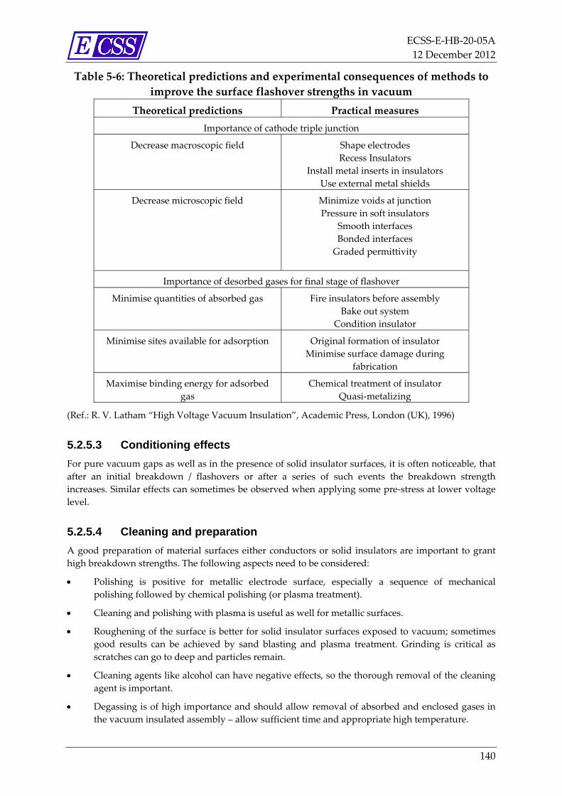
ECSS‐E‐HB‐20‐05A
12 December 2012
140
Table 5‐6: Theoretical predictions and experimental consequences of methods to
improve the surface flashover strengths in vacuum
Theoretical predictions Practical measures
Importance of cathode triple junction
Decrease macroscopic field Shape electrodes
Recess Insulators
Install metal inserts in insulators
Use external metal shields
Decrease microscopic field Minimize voids at junction
Pressure in soft insulators
Smooth interfaces
Bonded interfaces
Graded permittivity
Importance of desorbed gases for final stage of flashover
Minimise quantities of absorbed gas Fire insulators before assembly
Bake out system
Condition insulator
Minimise sites available for adsorption Original formation of insulator
Minimise surface damage during
fabrication
Maximise binding energy for adsorbed
gas
Chemical treatment of insulator
Quasi‐metalizing
(Ref.: R. V. Latham “High Voltage Vacuum Insulation”, Academic Press, London (UK), 1996)
5.2.5.3 Conditioning effects
For pure vacuum gaps as well as in the presence of solid insulator surfaces, it is often noticeable, that
after an initial breakdown / flashovers or after a series of such events the breakdown strength
increases. Similar effects can sometimes be observed when applying some pre‐stress at lower voltage
level.
5.2.5.4 Cleaning and preparation
A good preparation of material surfaces either conductors or solid insulators are important to grant
high breakdown strengths. The following aspects need to be considered:
Polishing is positive for metallic electrode surface, especially a sequence of mechanical
polishing followed by chemical polishing (or plasma treatment).
Cleaning and polishing with plasma is useful as well for metallic surfaces.
Roughening of the surface is better for solid insulator surfaces exposed to vacuum; sometimes
good results can be achieved by sand blasting and plasma treatment. Grinding is critical as
scratches can go to deep and particles remain.
Cleaning agents like alcohol can have negative effects, so the thorough removal of the cleaning
agent is important.
Degassing is of high importance and should allow removal of absorbed and enclosed gases in
the vacuum insulated assembly – allow sufficient time and appropriate high temperature.
ECSS‐E‐HB‐20‐05A
12 December 2012
141
Bake‐out of vacuum insulated systems is very positive and works well for ceramic and other
temperature withstanding materials.
The presence of particles is critical and should be avoided by the manufacturing and cleaning
process.
5.2.5.5 Leakage currents and triple-junction effect
Significant leakage current can occur already below the breakdown threshold of a vacuum insulated
system. The reason for this is small emission sites for electrons that can be found at locations with
surface inhomogenities (particles, defects, micro‐protrusions, sharp edges etc.). A very critical
emission site is typically found in the triple‐junction zones of the interface between conductor, solid
insulator and vacuum. Therefore it should be ensured by design and verified by test, that only
negligible emission currents are flowing.
5.2.5.6 Control of pressure
The control of pressure is most important for a vacuum insulated assembly, if the voltage exceeds the
minimum of the relevant Paschen curve (see Figure 4‐7), that is for air above 300 V and for inert gases
above 80 V. For this purpose the following aspects are of importance:
For most of the practical applications a vacuum environment of lower than 10‐3 Pa resp. 10‐5
mbar is well suited – in the non‐metric world this is often modified into 1,310‐3 Pa resp. 1,310‐5
mbar (coming from 1 Torr (0° C) = 133,322 Pascal (N/m2)).
With some margin in practical applications a vacuum environment of lower than 10‐2 Pa resp.
10‐4 mbar is acceptable.
Very high vacuum of lower than 10‐5 Pa resp. 10‐7 mbar is very well suited for long term
stability, but only achievable in sealed containment without the presence of organic material
and requiring a dedicated bake‐out process. This is applied in electron tubes, for example.
Higher pressures, 10‐2 Pa resp. 10‐4 mbar need to consider the Paschen breakdown as a limiting
factor (see section 4.3.4). Operation of vacuum insulated equipment should be considered only,
if this is driven by specific user constraints, for example in laser equipments or with electric
propulsion systems.
5.2.5.7 On ground testing
Ground testing of vacuum insulated equipments, which are not completely sealed, can be performed in:
a suitable vacuum chamber
ambient air conditions, if the design allows this kind of operation and if in addition to the
design rules of vacuum insulation also the design rules for gaseous insulations are fulfilled
specific gas environment which provide a similar good strength as the vacuum insulation.
Possible ideas is bagging the setup and filling the containment with pure SF6 or a SF6‐air
mixture.
5.2.5.8 Long-term stability
Under the assumption, that infrequent spurious effects (flashover, breakdown) are acceptable for the
user, the long‐term stability of vacuum insulation is excellent as there are no degradation effects. After
a spurious event the insulation properties recover or often improve. Well designed systems operating
in a safe pressure environment, well outgassed and/or baked out can withstand many years without
spurious events. In order to ensure long‐term stability a low pressure (see section 5.2.5.6) and
protection against electron / ion flow is recommended to be employed.
ECSS‐E‐HB‐20‐05A
12 December 2012
142
5.2.5.9 Reparability
Vacuum insulation is self‐healing after a breakdown, so typically no repair is needed even after a
failure. Furthermore, there is no degradation. If a vacuum insulated system is kept open – like
individual high voltage modules interconnected in an open design, parts can be easily exchanged for
maintenance. This is of course different, if the vacuum insulation is kept in a sealed vessel, like it is for
example the case for electron tubes.
5.2.5.10 References of vacuum insulations
In space mission vacuum insulations have been used for:
ERS C‐Band Radar ‐ this type of C‐Band radar was flown on two ESA radar earth observation mission
ERS1 (1991 till 2000) and ERS‐2 (from1995 on). Maximum high voltage was 15 kVDC. Potted high
voltage modules have been interconnected via open (vacuum insulated) connection points.
RADARSAT C‐Band Radar ‐This type of C‐Band radar was flown on a Canadian radar earth
observation mission. The HPA was built by Dornier (now EADS Astrium) based on the ERS design.
INTERGRAL ACS Power Front‐end ‐An array of front‐ends with 2 kV operating voltage have been
built for the instrumentation.
5.2.5.11 Costs
As no specific containments are needed – despite the advantage having some shielding around – a
vacuum insulated system is comparably cheap, especially for recurring designs. For higher voltages
(tentatively over 5 kV) there is considerable effort (no‐recurring costs for design and verification)
necessary to investigate an optimum design and materials composition to reduce the risk of spurious
effects (discharges, flashovers).
5.2.5.12 Recommendation for use
Vacuum insulation is a cost and mass efficient solution for all high voltage systems
which are not operated in the critical pressure regime (safe pressures below 10‐2 Pa) and
which can accept spurious effects (flashovers, discharges).
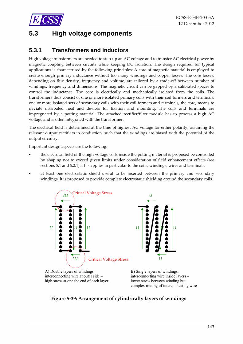
ECSS‐E‐HB‐20‐05A
12 December 2012
143
5.3 High voltage components
5.3.1 Transformers and inductors High voltage transformers are needed to step‐up an AC voltage and to transfer AC electrical power by
magnetic coupling between circuits while keeping DC isolation. The design required for typical
applications is characterised by the following principles: A core of magnetic material is employed to
create enough primary inductance without too many windings and copper losses. The core losses,
depending on flux density, frequency and volume, are tailored by a trade‐off between number of
windings, frequency and dimensions. The magnetic circuit can be gapped by a calibrated spacer to
control the inductance. The core is electrically and mechanically isolated from the coils. The
transformers thus consist of one or more isolated primary coils with their coil formers and terminals,
one or more isolated sets of secondary coils with their coil formers and terminals, the core, means to
deviate dissipated heat and devices for fixation and mounting. The coils and terminals are
impregnated by a potting material. The attached rectifier/filter module has to process a high AC
voltage and is often integrated with the transformer.
The electrical field is determined at the time of highest AC voltage for either polarity, assuming the
relevant output rectifiers in conduction, such that the windings are biased with the potential of the
output circuitry.
Important design aspects are the following:
the electrical field of the high voltage coils inside the potting material is proposed be controlled
by shaping not to exceed given limits under consideration of field enhancement effects (see
sections 5.1 and 5.2.1). This applies in particular to the coils, windings, wires and terminals.
at least one electrostatic shield useful to be inserted between the primary and secondary
windings. It is proposed to provide complete electrostatic shielding around the secondary coils.
Figure 5‐39: Arrangement of cylindrically layers of windings
A) Double layers of windings, interconnecting wire at outer side – high stress at one the end of each layer
U U U
2U
2U
Critical Voltage Stress
Critical Voltage Stress
U U U
U
U
B) Single layers of windings, interconnecting wire inside layers – lower stress between winding but complex routing of interconnecting wire
ECSS‐E‐HB‐20‐05A
12 December 2012
144
A typical high voltage transformer consists of a primary winding operating at low voltage and one or
more high voltage windings. For the high voltage side typically a high number of turns/windings are
required and the currents are low, thus the selected diameter of the wire is relatively low. The thin
wire in a stack of windings cause usually an inhomogeneous field, depending how the wire is routed,
and the related field stress can be very high. Some design aspects are explained in the following:
Layers of windings can be arranged in a cylindrical way as shown in Figure 5‐39. The different
layers of winding can be placed directly one above each other, either using a layer of insulation
material in‐between or without. Having no inter‐layer insulation results in a high stress
between individual wires of different layers due to a high voltage difference, which can be too
excessive for the wire insulation. The typical wire insulation is a coating or foil. Using an inter‐
layer insulation improves the situation. This additional insulation can be a foil or a sheet of fibre
material, which is later impregnated with a resin. In the example A) of the Figure 5‐4 the layers
of windings are arranged as double layers, which are easy to produce, however, this
configuration causes a higher insulation stress to every other ends of the windings layers. A
lower stress can be achieved by guiding an interconnecting wire always to the opposite end of
the windings space in‐between two layers of winds as shown in example B). However, routing
of the interconnecting wire requires more effort in manufacturing.
Layers of windings can be alternatively arranged in discs (sections) as shown in Figure 5‐40.
Each disc of windings is placed in a slot of a bobbin. The layers in the different discs can be
arranged differently: One possibility is the layout of double windings as shown in Figure 5‐40
A) another possibility is the layout of single windings switched in series as shown in B).
The distribution of voltage stress are different for cylindrical and sliced windings and the
advantages/disadvantages of each need to be assessed on a case‐by‐case basis considering AC
stress as well as other parameters as stray capacitance.
Critical zones of high electrical field strengths typically are found at the “high side: of a
configuration of windings (see example in Figure 5‐40 C). A compact stack of wires typically
shows a moderate electrical field strength inside, however, special attention should be paid to:
Corners of a stack – see zone (a) in Figure 5‐40 C)
Freestanding wires interconnecting to the “outside” ‐ see zone (b) in Figure 5‐40 C)
Displaced wires ” ‐ see zone (c) in Figure 5‐40 C)
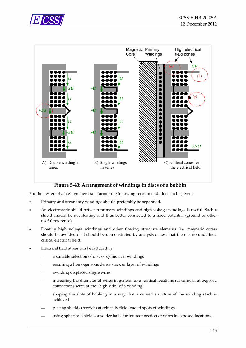
ECSS‐E‐HB‐20‐05A
12 December 2012
145
Figure 5‐40: Arrangement of windings in discs of a bobbin
For the design of a high voltage transformer the following recommendation can be given:
Primary and secondary windings should preferably be separated.
An electrostatic shield between primary windings and high voltage windings is useful. Such a
shield should be not floating and thus better connected to a fixed potential (ground or other
useful reference).
Floating high voltage windings and other floating structure elements (i.e. magnetic cores)
should be avoided or it should be demonstrated by analysis or test that there is no undefined
critical electrical field.
Electrical field stress can be reduced by
a suitable selection of disc or cylindrical windings
ensuring a homogeneous dense stack or layer of windings
avoiding displaced single wires
increasing the diameter of wires in general or at critical locations (at corners, at exposed
connections wire, at the “high side” of a winding
shaping the slots of bobbing in a way that a curved structure of the winding stack is
achieved
placing shields (toroids) at critically field loaded spots of windings
using spherical shields or solder balls for interconnection of wires in exposed locations.
A) Double winding in series
U
U
U
U
≈2U
≈2U
≈2U
U
U
U
≈U
≈U
≈U
B) Single windings in series
U
C) Critical zones for the electrical field
GND
HV
Primary Windings
Magnetic Core
High electrical field zones
(a)
(b)
(c)
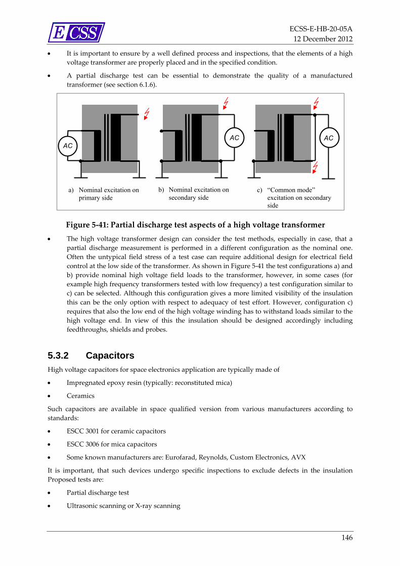
ECSS‐E‐HB‐20‐05A
12 December 2012
146
It is important to ensure by a well defined process and inspections, that the elements of a high
voltage transformer are properly placed and in the specified condition.
A partial discharge test can be essential to demonstrate the quality of a manufactured
transformer (see section 6.1.6).
Figure 5‐41: Partial discharge test aspects of a high voltage transformer
The high voltage transformer design can consider the test methods, especially in case, that a
partial discharge measurement is performed in a different configuration as the nominal one.
Often the untypical field stress of a test case can require additional design for electrical field
control at the low side of the transformer. As shown in Figure 5‐41 the test configurations a) and
b) provide nominal high voltage field loads to the transformer, however, in some cases (for
example high frequency transformers tested with low frequency) a test configuration similar to
c) can be selected. Although this configuration gives a more limited visibility of the insulation
this can be the only option with respect to adequacy of test effort. However, configuration c)
requires that also the low end of the high voltage winding has to withstand loads similar to the
high voltage end. In view of this the insulation should be designed accordingly including
feedthroughs, shields and probes.
5.3.2 Capacitors High voltage capacitors for space electronics application are typically made of
Impregnated epoxy resin (typically: reconstituted mica)
Ceramics
Such capacitors are available in space qualified version from various manufacturers according to
standards:
ESCC 3001 for ceramic capacitors
ESCC 3006 for mica capacitors
Some known manufacturers are: Eurofarad, Reynolds, Custom Electronics, AVX
It is important, that such devices undergo specific inspections to exclude defects in the insulation
Proposed tests are:
Partial discharge test
Ultrasonic scanning or X‐ray scanning
a) Nominal excitation on primary side
ACAC AC
b) Nominal excitation on secondary side
c) “Common mode” excitation on secondary side

ECSS‐E‐HB‐20‐05A
12 December 2012
147
Comparing ceramic capacitors and reconstituted mica capacitors it should be highlighted, that the
partial discharge thresholds for acceptance can be very different. For ceramics, partial discharge levels
below 5 pC (pico Coulomb) are typically applied, whereas for mica capacitors such acceptance levels
can be much higher as the material has a strong isotropic and brittle structure but is very resistant
against partial discharges.
Series switching of capacitors can ensure, that the distribution of voltage to the capacitor is well
balanced ensuring to be within the derating for static and repetitive stress cases and within rating for
transient stress cases. A useful measure is to switch bleeding resistors in parallel to each capacitor if
no other voltage control measures are applied. The dependence of the capacity to the applied voltage
is taken into account. For ceramic capacitors, the capacity decreases with an increasing voltage. In a
series of capacitance the lowest capacity supports the highest voltage that in turn decreases the
capacity increasing moreover the voltage imbalance.
Pulsed discharge currents typically should be limited in accordance with the parts specification. If
high pulse discharge currents are needed, parts with low inductivity should be preferred.
The environment around the capacitor should be properly controlled as most of the capacitors used
for high voltage electronics are not enclosed in metallic housing. This results in significant high
electrical fields (outside) around the parts. For a proper design this means:
Control the distance to neighbouring parts and structure elements including metal walls
Control the atmosphere around the component to avoid Paschen breakdown at critical pressure
or corona and to suppress partial discharges in general.
Some examples of critical cases and recommendations are shown in Figure 5‐42.
Despite the applications in electronic circuitry it is worth to mention that some of the capacitor
technology used in ground‐based high voltages applications are in principle suitable for space
applications as well, in specific:
Pressurized gas‐filled capacitors (low capacitance with high stability and low loss factor)
Liquid impregnated foils (like mineral oil/paper, mineral oil/ polymer foil).
Adaptation to space environment should especially consider adequate pressurization and leakage free
design and as well as radiation resistance.
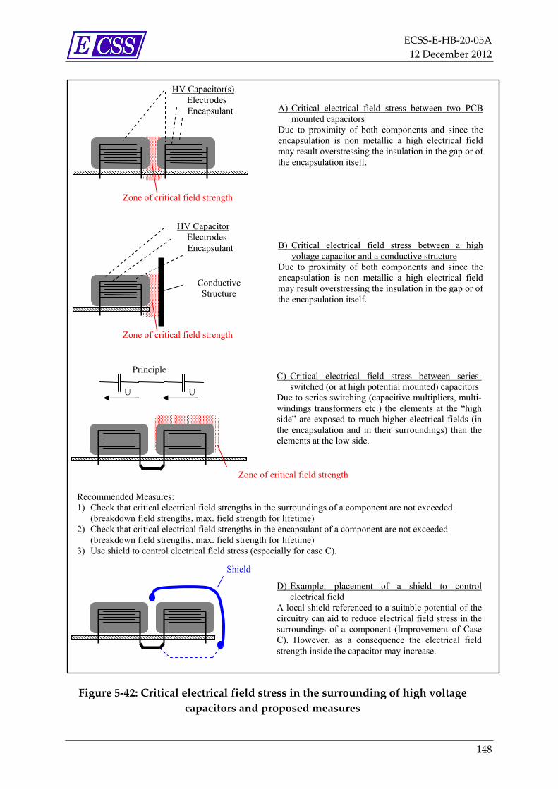
ECSS‐E‐HB‐20‐05A
12 December 2012
148
Figure 5‐42: Critical electrical field stress in the surrounding of high voltage
capacitors and proposed measures
A) Critical electrical field stress between two PCBmounted capacitors
Due to proximity of both components and since theencapsulation is non metallic a high electrical fieldmay result overstressing the insulation in the gap or ofthe encapsulation itself.
Zone of critical field strength
HV Capacitor(s) Electrodes
Encapsulant
B) Critical electrical field stress between a highvoltage capacitor and a conductive structure
Due to proximity of both components and since theencapsulation is non metallic a high electrical fieldmay result overstressing the insulation in the gap or ofthe encapsulation itself.
Zone of critical field strength
HV Capacitor Electrodes
Encapsulant
Conductive Structure
C) Critical electrical field stress between series-switched (or at high potential mounted) capacitors
Due to series switching (capacitive multipliers, multi-windings transformers etc.) the elements at the “highside” are exposed to much higher electrical fields (inthe encapsulation and in their surroundings) than theelements at the low side.
Zone of critical field strength
Principle
U U
Recommended Measures: 1) Check that critical electrical field strengths in the surroundings of a component are not exceeded
(breakdown field strengths, max. field strength for lifetime) 2) Check that critical electrical field strengths in the encapsulant of a component are not exceeded
(breakdown field strengths, max. field strength for lifetime) 3) Use shield to control electrical field stress (especially for case C).
D) Example: placement of a shield to controlelectrical field
A local shield referenced to a suitable potential of thecircuitry can aid to reduce electrical field stress in thesurroundings of a component (Improvement of CaseC). However, as a consequence the electrical fieldstrength inside the capacitor may increase.
Shield
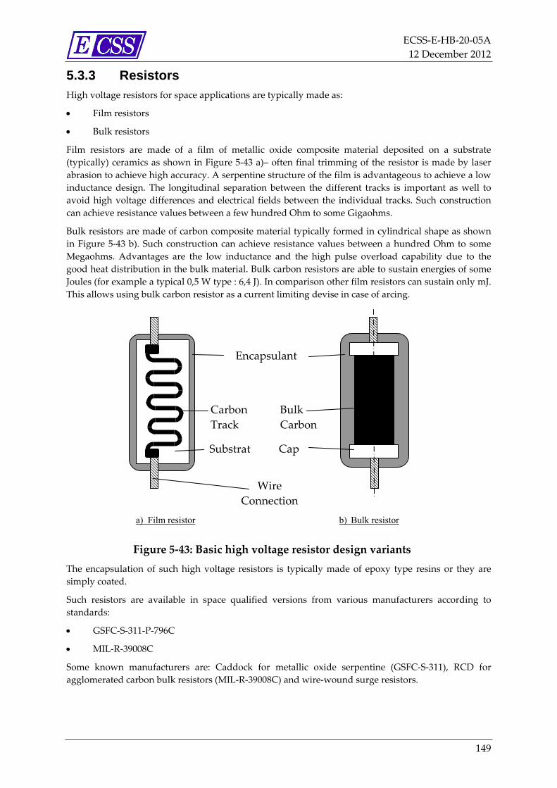
ECSS‐E‐HB‐20‐05A
12 December 2012
149
5.3.3 Resistors High voltage resistors for space applications are typically made as:
Film resistors
Bulk resistors
Film resistors are made of a film of metallic oxide composite material deposited on a substrate
(typically) ceramics as shown in Figure 5‐43 a)– often final trimming of the resistor is made by laser
abrasion to achieve high accuracy. A serpentine structure of the film is advantageous to achieve a low
inductance design. The longitudinal separation between the different tracks is important as well to
avoid high voltage differences and electrical fields between the individual tracks. Such construction
can achieve resistance values between a few hundred Ohm to some Gigaohms.
Bulk resistors are made of carbon composite material typically formed in cylindrical shape as shown
in Figure 5‐43 b). Such construction can achieve resistance values between a hundred Ohm to some
Megaohms. Advantages are the low inductance and the high pulse overload capability due to the
good heat distribution in the bulk material. Bulk carbon resistors are able to sustain energies of some
Joules (for example a typical 0,5 W type : 6,4 J). In comparison other film resistors can sustain only mJ.
This allows using bulk carbon resistor as a current limiting devise in case of arcing.
Figure 5‐43: Basic high voltage resistor design variants
The encapsulation of such high voltage resistors is typically made of epoxy type resins or they are
simply coated.
Such resistors are available in space qualified versions from various manufacturers according to
standards:
GSFC‐S‐311‐P‐796C
MIL‐R‐39008C
Some known manufacturers are: Caddock for metallic oxide serpentine (GSFC‐S‐311), RCD for
agglomerated carbon bulk resistors (MIL‐R‐39008C) and wire‐wound surge resistors.
a) Film resistor
Encapsulant
Carbon
Track
Bulk
Carbon
Substrat Cap
Wire
Connection
b) Bulk resistor
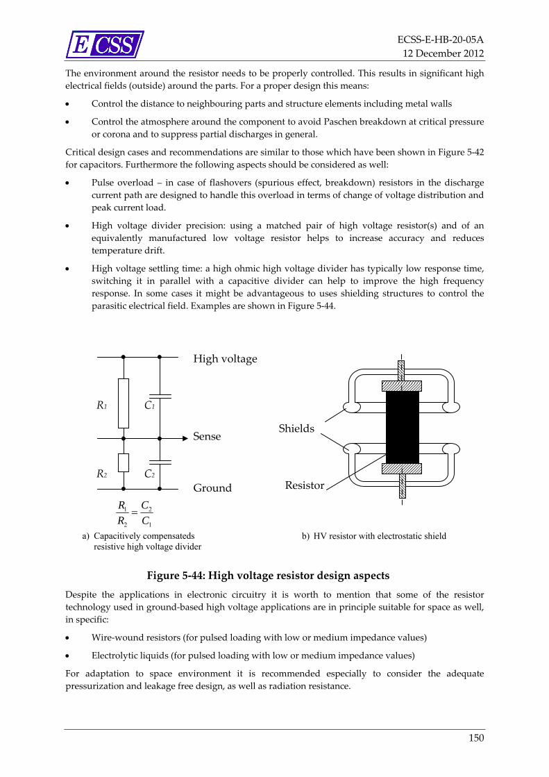
ECSS‐E‐HB‐20‐05A
12 December 2012
150
The environment around the resistor needs to be properly controlled. This results in significant high
electrical fields (outside) around the parts. For a proper design this means:
Control the distance to neighbouring parts and structure elements including metal walls
Control the atmosphere around the component to avoid Paschen breakdown at critical pressure
or corona and to suppress partial discharges in general.
Critical design cases and recommendations are similar to those which have been shown in Figure 5‐42
for capacitors. Furthermore the following aspects should be considered as well:
Pulse overload – in case of flashovers (spurious effect, breakdown) resistors in the discharge
current path are designed to handle this overload in terms of change of voltage distribution and
peak current load.
High voltage divider precision: using a matched pair of high voltage resistor(s) and of an
equivalently manufactured low voltage resistor helps to increase accuracy and reduces
temperature drift.
High voltage settling time: a high ohmic high voltage divider has typically low response time,
switching it in parallel with a capacitive divider can help to improve the high frequency
response. In some cases it might be advantageous to uses shielding structures to control the
parasitic electrical field. Examples are shown in Figure 5‐44.
Figure 5‐44: High voltage resistor design aspects
Despite the applications in electronic circuitry it is worth to mention that some of the resistor
technology used in ground‐based high voltage applications are in principle suitable for space as well,
in specific:
Wire‐wound resistors (for pulsed loading with low or medium impedance values)
Electrolytic liquids (for pulsed loading with low or medium impedance values)
For adaptation to space environment it is recommended especially to consider the adequate
pressurization and leakage free design, as well as radiation resistance.
a) Capacitively compensateds resistive high voltage divider
Resistor
Shields
b) HV resistor with electrostatic shield
Ground
Sense
High voltage
R1
R2
C1
C2
1
2
2
1
C
C
R
R
ECSS‐E‐HB‐20‐05A
12 December 2012
151
5.3.4 Semiconductors High voltage semiconductors for space electronics applications are typically
High voltage diodes/rectifiers (typically rated to several kV)
High voltage transistors (typically MOS‐FET´s rated up to 1000 V)
Such semiconductors are available in space qualified versions from various manufacturers according
to standards:
MIL‐PRF‐19500P
Some known suppliers are: Microsemi (US), Sensitron (US), VMI (US)
As long as such semiconductor components are not completely encapsulated and sealed in a metallic
housing the environment around the component should be properly controlled. As most
semiconductors used for high voltage electronics are not enclosed in metallic housings, there can be
significant high electrical fields present (outside) around the parts. For a proper design this means:
Control the distances to neighbouring parts and structure elements including metal walls
Control the atmosphere around the component to avoid Paschen breakdown at critical pressure
or corona and to suppress partial discharges in general.
Some examples of critical cases and recommendations are shown in Figure 5‐42 (demonstrated here
for capacitors).
It is worth to highlight also that leakages of some μA can impair the functionality well before the
electrical field breakdown.
Despite the applications in electronic circuitry it is worth to mention that some of the semiconductor
technology used in ground‐based high voltages application is in principle suitable for space as well, in
specific:
IGBT´s
Thyristors
Adaptation to space environment should especially consider adequate thermo‐mechanical design as
well as radiation resistance.
5.3.5 Wires and cables High voltage wires for space electronics application are typically made of
PTFE (Polytetrafluarethylene, Trademark: Teflon)
FEP (Fluorinated Ethylene Propylene)
Polyimide (Trademark: Kapton) ‐ typically for lower voltages (< 600 V)
PE ‐ Polyethylene (few applications)
Silicone elastomer
In fact, for most of the DC applications in space PTFE and FEP wires are used for a voltage range of
some kV up to the order of 20 kV. Polyimide is only used in the voltage range of a few hundred volts.
In a few exceptional applications silicone and PE insulations have been used. Sometimes, a silicon
material is used in combination with FEP to complement the properties of both. However, silicon
insulations are mechanically sensitive, whereas PE is critical with respect to radiation. Nevertheless
both can be attractive for AC applications, as it is possible to produce homogeneous conductive layers
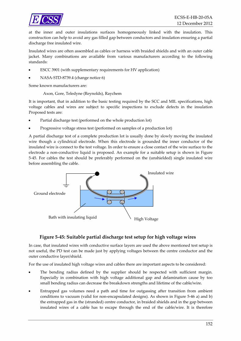
ECSS‐E‐HB‐20‐05A
12 December 2012
152
at the inner and outer insulations surfaces homogeneously linked with the insulation. This
construction can help to avoid any gas filled gap between conductors and insulation ensuring a partial
discharge free insulated wire.
Insulated wires are often assembled as cables or harness with braided shields and with an outer cable
jacket. Many combinations are available from various manufacturers according to the following
standards:
ESCC 3901 (with supplementary requirements for HV application)
NASA‐STD‐8739.4 (change notice 6)
Some known manufacturers are:
Axon, Gore, Teledyne (Reynolds), Raychem
It is important, that in addition to the basic testing required by the SCC and MIL specifications, high
voltage cables and wires are subject to specific inspections to exclude defects in the insulation
Proposed tests are:
Partial discharge test (performed on the whole production lot)
Progressive voltage stress test (performed on samples of a production lot)
A partial discharge test of a complete production lot is usually done by slowly moving the insulated
wire though a cylindrical electrode. When this electrode is grounded the inner conductor of the
insulated wire is connect to the test voltage. In order to ensure a close contact of the wire surface to the
electrode a non‐conductive liquid is proposed. An example for a suitable setup is shown in Figure
5‐45. For cables the test should be preferably performed on the (unshielded) single insulated wire
before assembling the cable.
Figure 5‐45: Suitable partial discharge test setup for high voltage wires
In case, that insulated wires with conductive surface layers are used the above mentioned test setup is
not useful, the PD test can be made just by applying voltages between the centre conductor and the
outer conductive layer/shield.
For the use of insulated high voltage wires and cables there are important aspects to be considered:
The bending radius defined by the supplier should be respected with sufficient margin.
Especially in combination with high voltage additional gap and delamination cause by too
small bending radius can decrease the breakdown strengths and lifetime of the cable/wire.
Entrapped gas volumes need a path and time for outgassing after transition from ambient
conditions to vacuum (valid for non‐encapsulated designs). As shown in Figure 5‐46 a) and b)
the entrapped gas in the (stranded) centre conductor, in braided shields and in the gap between
insulated wires of a cable has to escape through the end of the cable/wire. It is therefore
High VoltageBath with insulating liquid
Ground electrode
Insulated wire
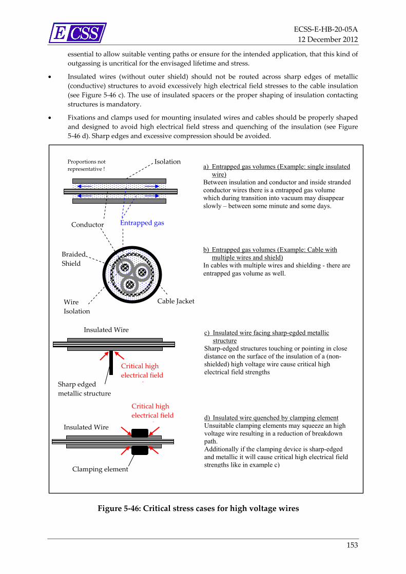
ECSS‐E‐HB‐20‐05A
12 December 2012
153
essential to allow suitable venting paths or ensure for the intended application, that this kind of
outgassing is uncritical for the envisaged lifetime and stress.
Insulated wires (without outer shield) should not be routed across sharp edges of metallic
(conductive) structures to avoid excessively high electrical field stresses to the cable insulation
(see Figure 5‐46 c). The use of insulated spacers or the proper shaping of insulation contacting
structures is mandatory.
Fixations and clamps used for mounting insulated wires and cables should be properly shaped
and designed to avoid high electrical field stress and quenching of the insulation (see Figure
5‐46 d). Sharp edges and excessive compression should be avoided.
Figure 5‐46: Critical stress cases for high voltage wires
b) Entrapped gas volumes (Example: Cable with multiple wires and shield)
In cables with multiple wires and shielding - there are entrapped gas volume as well.
Critical high
electrical field
h
Isolation
Conductor Entrapped gas
Proportions not
representative !
Braided
Shield
Wire
Isolation
Insulated Wire
a) Entrapped gas volumes (Example: single insulated wire)
Between insulation and conductor and inside stranded conductor wires there is a entrapped gas volume which during transition into vacuum may disappear slowly – between some minute and some days.
Sharp edged
metallic structure
Critical high
electrical field
hInsulated Wire
Clamping element
Cable Jacket
c) Insulated wire facing sharp-egded metallic structure
Sharp-edged structures touching or pointing in close distance on the surface of the insulation of a (non-shielded) high voltage wire cause critical high electrical field strengths
d) Insulated wire quenched by clamping element Unsuitable clamping elements may squeeze an high voltage wire resulting in a reduction of breakdown path. Additionally if the clamping device is sharp-edged and metallic it will cause critical high electrical field strengths like in example c)
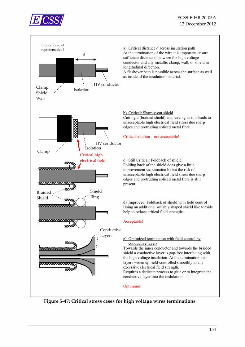
ECSS‐E‐HB‐20‐05A
12 December 2012
154
Figure 5‐47: Critical stress cases for high voltage wires terminations
d
Proportions not
representative ! a) Critical distance d across insulation path At the termination of the wire it is important ensure sufficient distance d between the high voltage conductor and any metallic clamp, wall, or shield in longitudinal direction. A flashover path is possible across the surface as well as inside of the insulation material.
Critical high
electrical field
h
Clamp
Shield,
Wall
Isolation
HV conductor
Clamp Isolation
HV conductor
b) Critical: Sharply-cut shield Cutting a (braided shield) and leaving as it is leads to unacceptable high electrical field stress due sharp edges and protruding spliced metal fibre. Critical solution – not acceptable!
c) Still Critical: Foldback of shield Folding back of the shield does give a little improvement vs. situation b) but the risk of unacceptable high electrical field stress due sharp edges and protruding spliced metal fibre is still present.
d) Improved: Foldback of shield with field control Using an additional suitably shaped shield like toroids help to reduce critical field strengths. Acceptable!
e) Optimized termination with field control by conductive layers
Towards the inner conductor and towards the braided shield a conductive layer is gap-free interfacing with the high voltage insulation. At the termination this layers widen up field-controlled smoothly to any excessive electrical field strength. Requires a dedicate process to glue or to integrate the conductive layer into the inslulation. Optimium!
Braided
Shield
Shield
Ring
Conductive
Layers
ECSS‐E‐HB‐20‐05A
12 December 2012
155
For the termination of high voltage wire there are as well some important aspects to consider:
At the cut end of a high voltage wire the distance d between the inner conductor and the cut
shield or to any other related structure should be sufficient to avoid
Surface flashover
Internal breakdown of the insulation in lateral direction
(see Figure 5‐47 a).
As an orientation the field strengths in lateral direction should not exceed 400V/mm (air, high
vacuum and equivalent surroundings) under worst case assumption for tolerances of workman
ship. It is highlighted, that even embedding of this termination into a potting material gives a
vulnerable interface, and excessive field loads should be strictly avoided.
For shielded wires – especially with a braided shield – attention is paid to the fact that the
shield is not just cut, as the cut region naturally forms a sharp electrode close to the insulation
surface and a single protruding strand causes an (additional) increase in the local electrical
field. The Situation as shown in Figure 5‐47 b) should be strictly avoided.
Back folding of the shield (as shown in Figure 5‐47 c)) can give a slightly improved situation,
however, the real curvature cannot be well controlled and the splicing and protruding of single
strands cannot be avoided systematically.
A shield electrode (as shown in Figure 5‐47 d)) can help to “shade” the critical area of shield
termination, however, zones with gaps between shield/electrode and insulation can be
vulnerable to partial discharge inception.
For higher DC and AC voltages it is necessary to glue or to integrate a conductive layer (i.e.
carbon) into the interface to the conductor and to the braided shield ‐ as shown in Figure 5‐47 e).
This design avoids any gap between conductor and insulation. Both layers should be opened up
at the termination, thus increasing the distance while limiting the electrical field strength. Such
complex integrated shields require a suitable production process of the HV wire and of the
termination. Extruding processes of silicon or polyethylene insulation are suitable for such type
of field control. Insulations built up with tapes and layers are suitable as well. This type of field
control is proposed for AC voltage higher than 1 kV and DC voltage higher than 20..30 kV
(orientation values!).
Often the termination of a high voltage wire is embedded into a potting material, where some specific
aspects (in addition to the above mentioned) should be taken into consideration:
A good adhesion between the wire insulation and the potting material should be ensured. Often
a primer is used for this purpose (with FPA, PTFE, Silicone insulated wires). Surface
roughening for example with plasma treatment can be useful in some cases. Proper cleaning
and outgassing (before potting) is clearly mandatory as well.
A good mechanical compatibility should be ensured, especially when potting wire with a soft
insulation material into a hard potting (silicone‐epoxy, PTFE epoxy). Sometimes shrinkage
sleeves are used as a stress‐relief – however, it needs to be controlled, that this construction is
not weakening the electrical strengths.
In order to prevent that mechanical forces on the wire leading to delaminate it from the potting
material, it is proposed to glue or tie‐base the wire on the potting surface.
ECSS‐E‐HB‐20‐05A
12 December 2012
156
5.3.6 Connectors High voltage connectors for ground operation (ambient pressure) are available in many variants for
voltages up to a few ten kV, for higher voltages as single‐pin for moderate and low voltage as multi‐
pin connectors.
For operation in vacuum the choice of suitable connectors is very limited. The main problem for the
design of such a connector is the interface between the interlaced insulation of the plug and the
receptacle. Three strategies for the design of this interlaced interface should be taken into
consideration:
Gapless interface of plug and receptacle insulation, by using slightly conical structures with a
soft insulation material in‐between
Interface with vented gap
Interface with hermetically sealed gap
The gapless interface is difficult to achieve as it requires high precision of the manufacturing and a
suitable soft insulation material for the interface.
Using a connector with a vented gap is only operating stably, if the critical pressure range in the
interface can be avoided, i.e. by sufficient outgassing time in a high vacuum environment before
applying high voltage. The vented gap becomes critical under ambient environment if the inception
threshold for partial discharges is exceeded and especially if an AC voltage is applied.
A hermetically sealed interface can grant stable operating conditions for short‐term independent of
probably critical pressure outside, however, can reach a critical pressure due to leakage after long‐
term exposition in space vacuum.
In general, it should be highlighted, that the availability of space‐qualified connectors is very limited.
As a conclusion, the appropriate connector design (if available) is depending on the intended use.
Gapless interface and hermetically sealed gap interface can be suitable for short‐term applications
(more) independent of the pressure environment, whereas vented gaps for long‐term operation are
better if used after a good outgassing in a high vacuum environment.
In addition to the interface between plug and receptacle, the interface between plug/socket and the
attached cable is very essential. Typically a gap‐free interface should be achieved, for example by a
suitable potting/gluing process. As this interface is very critical and requires a very well defined
process it is mostly unavoidable to procure a connector assembly together with the cable from one
supplier. Matching cables and connectors from different sources is very risky and typically not
reliable.
Space suitable high voltage connectors seem today only available from the company Teledyne
incorporating the former entities Rowe and Reynolds. Although there have been single products used
on European space missions (from the “600 series” and from “PeeWee series”), there is no general
space‐qualified product available.
It is important, that in addition to the basic testing required by the SCC and MIL specifications, high
voltage connector‐cable assemblies are subject to specific inspections to exclude defects in the
insulation Proposed tests are:
Partial discharge test (performed on the entire production lot)
Progressive voltage stress test (performed on samples of a production lot)
Leakage current measurement (performed on the entire production lot)
Life test on samples considering the typical environmental conditions (temperature and
pressure).
Burn‐in test on assemblies dedicated to be used on flight.
ECSS‐E‐HB‐20‐05A
12 December 2012
157
5.3.7 Interconnections As an alternative to high voltage connectors there are other methods of interconnection which can
have the advantage of simplification and lower risk – if properly selected and applied.
Solder terminals
Screwed of clamped terminals
Flying leads (soldered or crimped)
Terminals dedicated to solder joints or to bolted/clamped fixation as shown in Figure 5‐49 a) and b)
are suitable if used in a high vacuum environment (or if designed for that) under ambient conditions.
For solder joints with a spherical shape of the solder joint is proposed. Especially for voltage higher
than a few kV and addition shield should be used (see example in Figure 5‐49 c). In principle these
kinds of connections are detachable. Additional encapsulation with a potting material makes the
connection suitable for critical pressure environment, however, is not limiting the reparability.
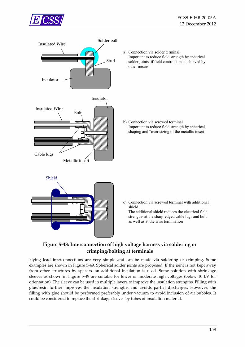
ECSS‐E‐HB‐20‐05A
12 December 2012
158
Figure 5‐48: Interconnection of high voltage harness via soldering or
crimping/bolting at terminals
Flying lead interconnections are very simple and can be made via soldering or crimping. Some
examples are shown in Figure 5‐49. Spherical solder joints are proposed. If the joint is not kept away
from other structures by spacers, an additional insulation is used. Some solution with shrinkage
sleeves as shown in Figure 5‐49 are suitable for lower or moderate high voltages (below 10 kV for
orientation). The sleeve can be used in multiple layers to improve the insulation strengths. Filling with
glue/resin further improves the insulation strengths and avoids partial discharges. However, the
filling with glue should be performed preferably under vacuum to avoid inclusion of air bubbles. It
could be considered to replace the shrinkage sleeves by tubes of insulation material.
Insulated Wire
a) Connection via solder terminal Important to reduce field strength by spherical solder joints, if field control is not achieved by other means
Insulator
Stud
Solder ball
Insulated Wire
Insulator
Cable lugs
Bolt
Metallic insert
b) Connection via screwed terminal Important to reduce field strength by spherical shaping and “over sizing of the metallic insert
c) Connection via screwed terminal with additional shield The additional shield reduces the electrical field strengths at the sharp-edged cable lugs and bolt as well as at the wire termination
Shield
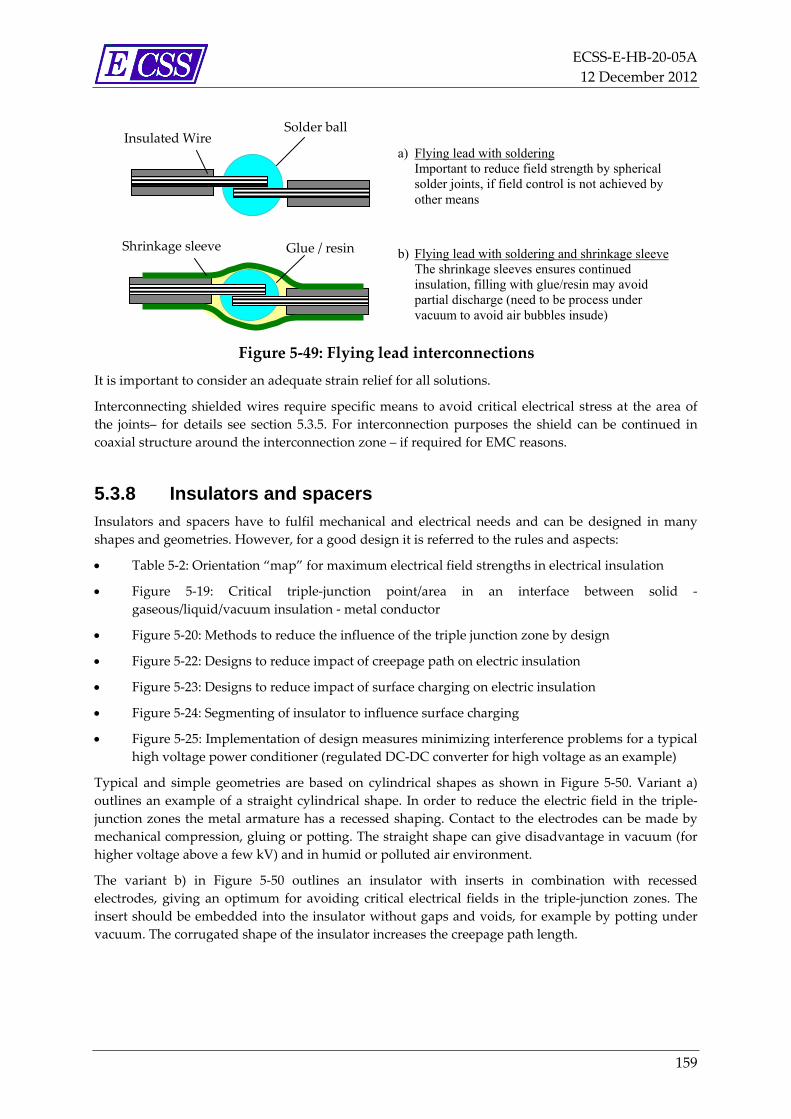
ECSS‐E‐HB‐20‐05A
12 December 2012
159
Figure 5‐49: Flying lead interconnections
It is important to consider an adequate strain relief for all solutions.
Interconnecting shielded wires require specific means to avoid critical electrical stress at the area of
the joints– for details see section 5.3.5. For interconnection purposes the shield can be continued in
coaxial structure around the interconnection zone – if required for EMC reasons.
5.3.8 Insulators and spacers
Insulators and spacers have to fulfil mechanical and electrical needs and can be designed in many
shapes and geometries. However, for a good design it is referred to the rules and aspects:
Table 5‐2: Orientation “map” for maximum electrical field strengths in electrical insulation
Figure 5‐19: Critical triple‐junction point/area in an interface between solid ‐
gaseous/liquid/vacuum insulation ‐ metal conductor
Figure 5‐20: Methods to reduce the influence of the triple junction zone by design
Figure 5‐22: Designs to reduce impact of creepage path on electric insulation
Figure 5‐23: Designs to reduce impact of surface charging on electric insulation
Figure 5‐24: Segmenting of insulator to influence surface charging
Figure 5‐25: Implementation of design measures minimizing interference problems for a typical
high voltage power conditioner (regulated DC‐DC converter for high voltage as an example)
Typical and simple geometries are based on cylindrical shapes as shown in Figure 5‐50. Variant a)
outlines an example of a straight cylindrical shape. In order to reduce the electric field in the triple‐
junction zones the metal armature has a recessed shaping. Contact to the electrodes can be made by
mechanical compression, gluing or potting. The straight shape can give disadvantage in vacuum (for
higher voltage above a few kV) and in humid or polluted air environment.
The variant b) in Figure 5‐50 outlines an insulator with inserts in combination with recessed
electrodes, giving an optimum for avoiding critical electrical fields in the triple‐junction zones. The
insert should be embedded into the insulator without gaps and voids, for example by potting under
vacuum. The corrugated shape of the insulator increases the creepage path length.
Insulated Wire a) Flying lead with soldering
Important to reduce field strength by spherical solder joints, if field control is not achieved by other means Stud
Solder ball
Shrinkage sleeve
Stud
Glue / resin b) Flying lead with soldering and shrinkage sleeve The shrinkage sleeves ensures continued insulation, filling with glue/resin may avoid partial discharge (need to be process under vacuum to avoid air bubbles insude)
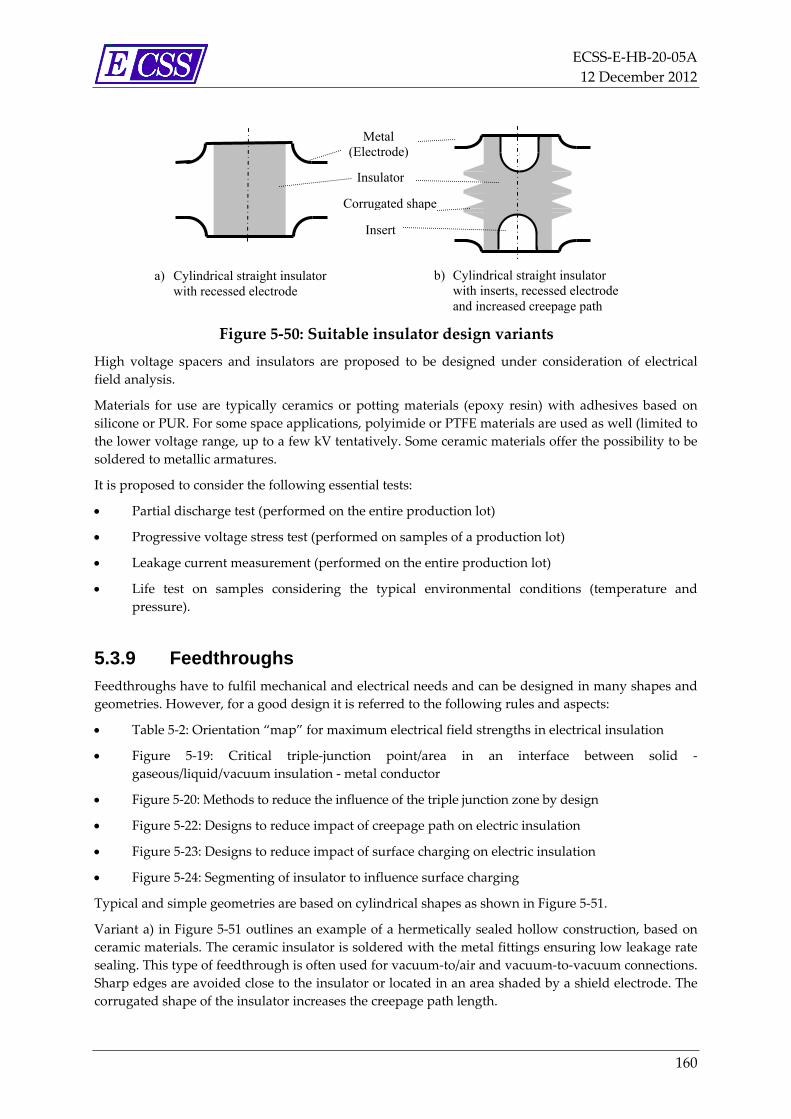
ECSS‐E‐HB‐20‐05A
12 December 2012
160
Figure 5‐50: Suitable insulator design variants
High voltage spacers and insulators are proposed to be designed under consideration of electrical
field analysis.
Materials for use are typically ceramics or potting materials (epoxy resin) with adhesives based on
silicone or PUR. For some space applications, polyimide or PTFE materials are used as well (limited to
the lower voltage range, up to a few kV tentatively. Some ceramic materials offer the possibility to be
soldered to metallic armatures.
It is proposed to consider the following essential tests:
Partial discharge test (performed on the entire production lot)
Progressive voltage stress test (performed on samples of a production lot)
Leakage current measurement (performed on the entire production lot)
Life test on samples considering the typical environmental conditions (temperature and
pressure).
5.3.9 Feedthroughs Feedthroughs have to fulfil mechanical and electrical needs and can be designed in many shapes and
geometries. However, for a good design it is referred to the following rules and aspects:
Table 5‐2: Orientation “map” for maximum electrical field strengths in electrical insulation
Figure 5‐19: Critical triple‐junction point/area in an interface between solid ‐
gaseous/liquid/vacuum insulation ‐ metal conductor
Figure 5‐20: Methods to reduce the influence of the triple junction zone by design
Figure 5‐22: Designs to reduce impact of creepage path on electric insulation
Figure 5‐23: Designs to reduce impact of surface charging on electric insulation
Figure 5‐24: Segmenting of insulator to influence surface charging
Typical and simple geometries are based on cylindrical shapes as shown in Figure 5‐51.
Variant a) in Figure 5‐51 outlines an example of a hermetically sealed hollow construction, based on
ceramic materials. The ceramic insulator is soldered with the metal fittings ensuring low leakage rate
sealing. This type of feedthrough is often used for vacuum‐to/air and vacuum‐to‐vacuum connections.
Sharp edges are avoided close to the insulator or located in an area shaded by a shield electrode. The
corrugated shape of the insulator increases the creepage path length.
a) Cylindrical straight insulator with recessed electrode
Metal (Electrode)
b) Cylindrical straight insulator with inserts, recessed electrode and increased creepage path
Insulator
Insert
Corrugated shape
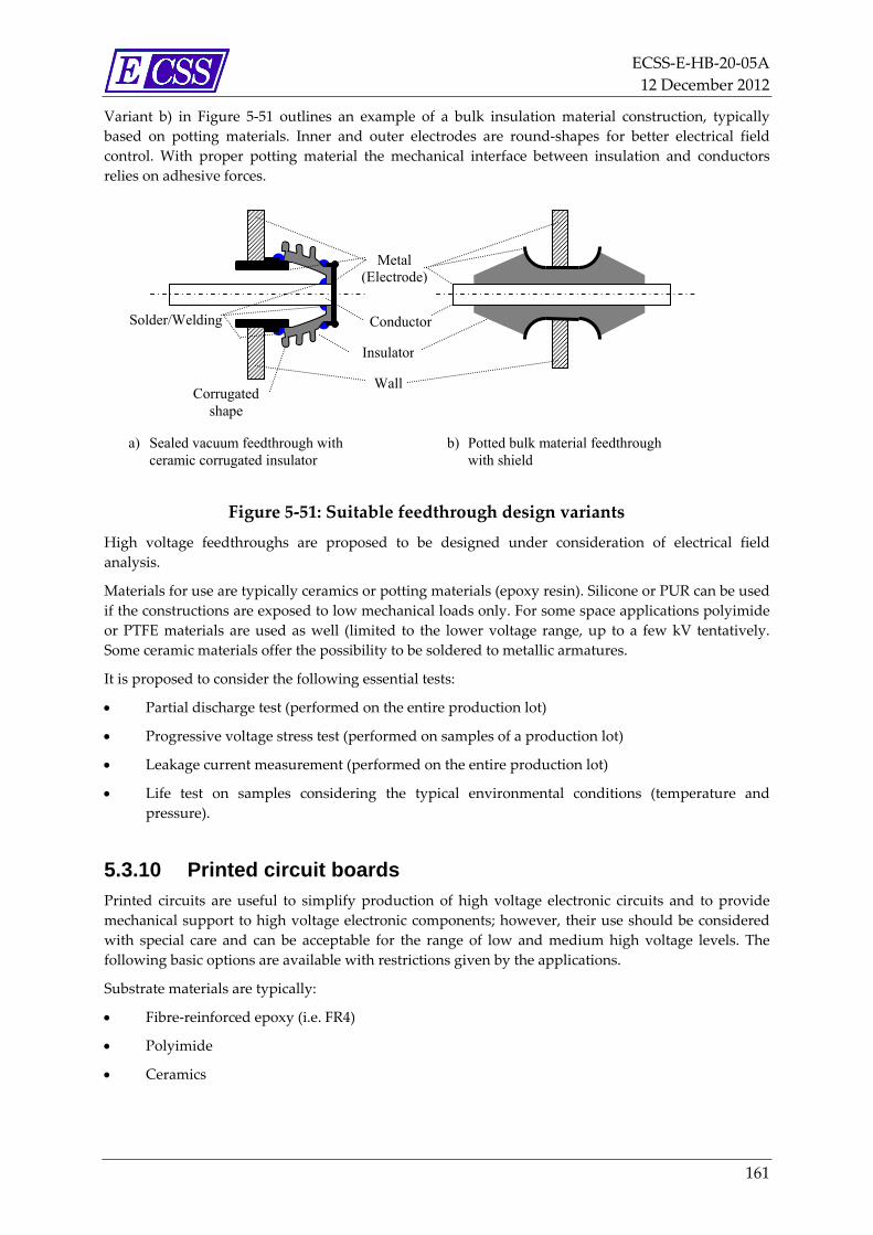
ECSS‐E‐HB‐20‐05A
12 December 2012
161
Variant b) in Figure 5‐51 outlines an example of a bulk insulation material construction, typically
based on potting materials. Inner and outer electrodes are round‐shapes for better electrical field
control. With proper potting material the mechanical interface between insulation and conductors
relies on adhesive forces.
Figure 5‐51: Suitable feedthrough design variants
High voltage feedthroughs are proposed to be designed under consideration of electrical field
analysis.
Materials for use are typically ceramics or potting materials (epoxy resin). Silicone or PUR can be used
if the constructions are exposed to low mechanical loads only. For some space applications polyimide
or PTFE materials are used as well (limited to the lower voltage range, up to a few kV tentatively.
Some ceramic materials offer the possibility to be soldered to metallic armatures.
It is proposed to consider the following essential tests:
Partial discharge test (performed on the entire production lot)
Progressive voltage stress test (performed on samples of a production lot)
Leakage current measurement (performed on the entire production lot)
Life test on samples considering the typical environmental conditions (temperature and
pressure).
5.3.10 Printed circuit boards Printed circuits are useful to simplify production of high voltage electronic circuits and to provide
mechanical support to high voltage electronic components; however, their use should be considered
with special care and can be acceptable for the range of low and medium high voltage levels. The
following basic options are available with restrictions given by the applications.
Substrate materials are typically:
Fibre‐reinforced epoxy (i.e. FR4)
Polyimide
Ceramics
a) Sealed vacuum feedthrough with ceramic corrugated insulator
Metal (Electrode)
Insulator
Solder/Welding
Corrugated shape
Wall
Conductor
b) Potted bulk material feedthrough with shield
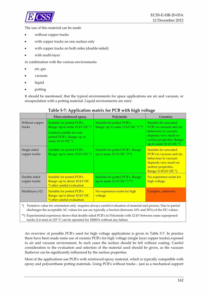
ECSS‐E‐HB‐20‐05A
12 December 2012
162
The use of this material can be made
without copper tracks
with copper tracks on one surface only
with copper tracks on both sides (double‐sided)
with multi‐layer
in combination with the various environments
air, gas
vacuum.
liquid
potting
It should be mentioned, that the typical environments for space applications are air and vacuum, or
encapsulation with a potting material. Liquid environments are rarer.
Table 5‐7: Application matrix for PCB with high voltage
Fibre‐reinforced epoxy Polyimide Ceramics
Without copper
tracks
Suitable for potted PCB’s.
Range: up to some 10 kV‐DC *)
Limited suitable for non‐
potted PCB’s. Range: up to
some 10 kV‐DC *)
Suitable for potted PCB’s.
Range: up to some 12 kV‐DC *) **)
Suitable for uncoated
PCB’s in vacuum and air,
behaviour in vacuum
depends very much on
surface properties. Range:
up to some 10 kV‐DC *)
Single sided
copper tracks
Suitable for potted PCB’s.
Range: up to some 10 kV‐DC *)
Suitable for potted PCB’s. Range:
up to some 12 kV‐DC *)**)
Suitable for uncoated
PCB’s in vacuum and air,
behaviour in vacuum
depends very much on
surface properties.
Range: 0‐30 kV‐DC *)
Double sided
copper tracks
Suitable for potted PCB’s
Range: up to about 10 kV‐DC
*) after careful evaluation
Suitable for potted PCB’s. Range:
up to some 12 kV‐DC *) **)
No experience exists for
high voltage
Multilayer (>2) Suitable for potted PCB’s.
Range: up to about 10 kV‐DC
*) after careful evaluation.
No experience exists for high
voltage
Complex, unknown
*) Tentative value for orientation only ‐requires always careful evaluation of material and process. Due to partial
discharges the acceptable AC values for use are typically a fraction (between 10% and 50%) of the DC‐values.
**) Experimental experience shows that double‐sided PCB’s in Polyimide with 12 kV between some superposed
tracks (1,6 mm) at 125 °C can be operated for 10000 h without any failure
An overview of possible PCB’s used for high voltage applications is given in Table 5‐7. In practice
there have been made some use of ceramic PCB’s for high voltage (single layer copper tracks) exposed
to air and vacuum environment. In such cases the surface should be left without coating. Careful
consideration to the evaluation and selection of the material used should be given, as the vacuum
flashover can be significantly influenced by the surface properties.
Most of the applications use PCB’s with reinforced epoxy material, which is typically compatible with
epoxy and polyurethane potting materials. Using PCB’s without tracks – just as a mechanical support
ECSS‐E‐HB‐20‐05A
12 December 2012
163
structure for mounted components ‐ enables the use up to a few ten kV DC voltage. Mounting can be
eased by small through holes and solder pads. Single layer and double layer constructions can be used
typically up to 12 kV‐DC (rough order of magnitude) however, preconditions are very well evaluated
and controlled material and processes. The design aspects outlined in Figure 5‐29: “Potting of PCB`s:
typical design aspects” should be regarded.
PCB’s with copper tracks on both sides rely on the crack‐free, void‐free insulation between both sides
represented by the board. This requires high attention to quality insurance by a well controlled
production process of the board, and inspections or test. Suitable means are
ultrasonic scanning
X‐ray scanning
partial discharge testing of the copper covered board before etching.
As in many cases the PCB’s are procured items from external suppliers it is essential to have visibility
on the board production process and introduce necessary inspections and tests.
Multi‐layers PCB’s with more than 2 layers usually use layers “sandwiches” of prepreg (impregnated
glass fibre mesh) and polyimide sheet to separate the different copper layers. As it is difficult to
produce such insulation structure void‐free it is not recommended to use such technology for voltages
higher than about 100 V. In general attention should be paid to vias and through holes as they can
create a significant lateral field stress to neighbouring copper layers. This constellation is very
sensitive and weak.
Non‐specific for high voltage the ECSS‐Q‐ST‐70‐10C and ECSS‐Q‐ST‐70‐11C apply however,
additional process control, screening and testing is proposed.
It is proposed to consider the following essential tests:
Partial discharge test (performed on the entire production lot)
Progressive voltage stress test (performed on samples of a production lot)
Leakage current measurement (performed on the entire production lot)
Life test on samples considering the typical environmental conditions (temperature and
pressure).
The partial discharge test is often difficult to perform on an etched and finished PCB it can be an
option for a raw double‐sided or for a single‐sided PCB to perform such a test before etching, this can
ensure, that the bulk insulation is checked to be free of partial discharges.
5.3.11 Other components Other possible high voltage components onboard spacecrafts are:
Electron tubes for RF amplification
Electron tubes for high power switching
Gas lasers.
In general for these complex devices the guidelines of this document about insulation, design and
materials apply in general, however, their specific application is subject of the knowledge and
experience of the manufacturers of these devices.
ECSS‐E‐HB‐20‐05A
12 December 2012
164
6 High voltage testing
6.1 Non-Destructive Testing
6.1.1 Insulation Resistance Test (INR)
6.1.1.1 Applicability
This test is a general test for all types of insulations. It can be used for the characterization of pure
insulations as well as for integrated circuitry. The insulation resistance test is useful to be done prior
and after high voltage testing to compare the state of insulation as well as initial test after integration
of high voltage circuits before applying high voltage.
6.1.1.2 Objectives
This test is used to characterize the quality of the insulation and to determine the critical state of the
insulation which makes risks visible of early failure or breakdown/short circuit.
6.1.1.3 Rationale
The test should be performed before applying high voltage for testing purpose or before first nominal
operation.
6.1.1.4 Method
The insulation resistance is tested by applying a low voltage (50 V to 100 V DC) to the insulation. An
instrument sensitive enough to detect picoamperes (pA) measures the resulting current and the
insulation resistance is calculated from Ohmʹs law (either by the measurement device or manually).
6.1.1.5 Acceptance Criteria
Insulation resistance should be higher than 1000 MΩ for a “pure” insulation.
This criterion can be modified accordingly, if the insulation is embedded in an environment which
makes it impossible to achieve this value, for example: if the insulation is part of an electronic circuitry
which provides low conductive paths in parallel to the insulation (e.g. resistors, semiconductors,
conductive layers).
6.1.1.5.1 Accuracy
Resistance: 5 %
6.1.1.5.2 Nonconformances
A failure of this test can require detailed investigations about the reason. Application of high voltage
to the circuit should be avoided, except in case of a failure investigation plan.
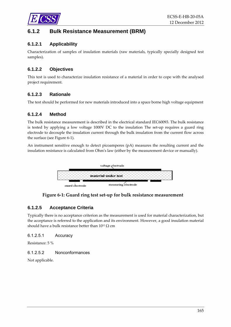
ECSS‐E‐HB‐20‐05A
12 December 2012
165
6.1.2 Bulk Resistance Measurement (BRM)
6.1.2.1 Applicability
Characterization of samples of insulation materials (raw materials, typically specially designed test
samples).
6.1.2.2 Objectives
This test is used to characterize insulation resistance of a material in order to cope with the analysed
project requirement.
6.1.2.3 Rationale
The test should be performed for new materials introduced into a space borne high voltage equipment
6.1.2.4 Method
The bulk resistance measurement is described in the electrical standard IEC60093. The bulk resistance
is tested by applying a low voltage 1000V DC to the insulation The set‐up requires a guard ring
electrode to decouple the insulation current through the bulk insulation from the current flow across
the surface (see Figure 6‐1).
An instrument sensitive enough to detect picoamperes (pA) measures the resulting current and the
insulation resistance is calculated from Ohmʹs law (either by the measurement device or manually).
Figure 6‐1: Guard ring test set‐up for bulk resistance measurement
6.1.2.5 Acceptance Criteria
Typically there is no acceptance criterion as the measurement is used for material characterization, but
the acceptance is referred to the application and its environment. However, a good insulation material
should have a bulk resistance better than 1012 Ω cm
6.1.2.5.1 Accuracy
Resistance: 5 %
6.1.2.5.2 Nonconformances
Not applicable.
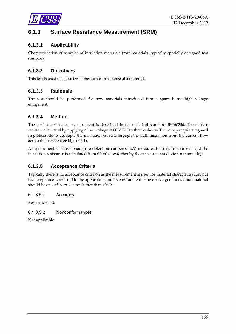
ECSS‐E‐HB‐20‐05A
12 December 2012
166
6.1.3 Surface Resistance Measurement (SRM)
6.1.3.1 Applicability
Characterization of samples of insulation materials (raw materials, typically specially designed test
samples).
6.1.3.2 Objectives
This test is used to characterise the surface resistance of a material.
6.1.3.3 Rationale
The test should be performed for new materials introduced into a space borne high voltage
equipment.
6.1.3.4 Method
The surface resistance measurement is described in the electrical standard IEC60250. The surface
resistance is tested by applying a low voltage 1000 V DC to the insulation The set‐up requires a guard
ring electrode to decouple the insulation current through the bulk insulation from the current flow
across the surface (see Figure 6‐1).
An instrument sensitive enough to detect picoamperes (pA) measures the resulting current and the
insulation resistance is calculated from Ohmʹs law (either by the measurement device or manually).
6.1.3.5 Acceptance Criteria
Typically there is no acceptance criterion as the measurement is used for material characterization, but
the acceptance is referred to the application and its environment. However, a good insulation material
should have surface resistance better than 109 Ω.
6.1.3.5.1 Accuracy
Resistance: 5 %
6.1.3.5.2 Nonconformances
Not applicable.
ECSS‐E‐HB‐20‐05A
12 December 2012
167
6.1.4 Polarisation and Depolarisation Current Measurement (PDC)
6.1.4.1 Applicability
This test is a general test for all types of insulations. It can be used for the characterization of whole
insulation systems. The polarisation (relaxation) test is useful to be done prior and after ageing/burn
in to compare the state of insulation.
6.1.4.2 Objectives
This test is used to characterize the quality of the insulation and to determine the critical state of the
insulation which makes risks visible of early failure or breakdown/short circuit.
6.1.4.3 Rationale
The test should be performed in nominal environment e.g. vacuum.
6.1.4.4 Method
The relaxation current is measured by applying a high voltage pulse (e.g. up to 2xUnom DC) to the
insulation. An instrument sensitive enough to detect picoamperes (pA) measures the resulting
current. For low capacitance high insulating DUT the duration of the high voltage should be no less
than 10 minutes. After switching off the voltage, the depolarisation current can be measured for
additional information.
6.1.4.5 Acceptance Criteria
Insulation current should be not greater than 100 pA after 10 minutes for low capacitance insulation
devices. No discontinuous current changes should occur.
This criterion can be modified accordingly, if the insulation is embedded in an environment which
makes it impossible to achieve this value, for example: if the insulation is part of an electronic circuitry
which provides low conductive paths in parallel to the insulation (resistors, semiconductors,
conductive layers, etc.).
6.1.4.5.1 Accuracy
Current: 5 %
6.1.4.5.2 Nonconformances
A failure of this test can require detailed investigations about the reason.
ECSS‐E‐HB‐20‐05A
12 December 2012
168
6.1.5 Dielectric Loss Factor Test (DLF)
6.1.5.1 Applicability
The dielectric loss factor measurement is used for characterization of samples of insulation material
(raw material, typically specially designed test samples) or of high voltage components like high
voltage cable, insulators and capacitors.
6.1.5.2 Objectives
This test is used to characterise insulation loss factor of a material or a component.
6.1.5.3 Rationale
The test should be performed for new materials introduced into a space borne high voltage equipment
or selected components.
6.1.5.4 Method
The dielectric measurement is described in the electrical standard IEC60250.
6.1.5.5 Acceptance Criteria
Typically there is no acceptance criterion as the measurement is used for material characterization, but
the acceptance is referred to the application and its environment. However, a good insulation material
should have dielectric loss factor better than 0,01 at 1 kHz.
6.1.5.5.1 Accuracy
Loss factor: 5 %
6.1.5.5.2 Nonconformances
not applicable.
ECSS‐E‐HB‐20‐05A
12 December 2012
169
6.1.6 Partial Discharge Test (PDT)
6.1.6.1 Objective
The objective is to qualitatively assess the insulation for presence of voids, cracks, particles,
delamination and workmanship.
6.1.6.2 Rationale
Partial discharge testing can be performed with AC voltages, DC voltages and ramp voltages.
Typically the use of an AC voltage is the most efficient method to detect voids and cracks within
insulation.
Testing with AC voltage should be the first choice, even if the nominal operation of the high voltage
device under test is not an AC voltage. However, if AC voltage is used instead of a DC voltage it
should be ensured that the electrical stress to insulation and embedded components does not exceed
the rated maximum voltage, and is from the electrical field strength equivalent to the original stress
situation.
It is important to ensure, that the background noise level of the facility are adequately low to allow a
precise measurement. For most cases, background noise levels below 1 pC are only achievable with a
high effort.
A criteria for a measurement is the acceptance of less than 5 pC, the facility should achieve a
background noise levels below 2 pC.
6.1.6.3 Method and Acceptance Criteria
The general principle and test method is described under:
IEC 60270:2000/BS EN 60270:2001 ʺHigh‐Voltage Test Techniques ‐ Partial Discharge Measurementsʺ
should be used.
The test is divided into two phases: addressing two different levels of testing:
Level 1 testing is used for general acceptance testing of assemblies with high voltage circuits or
to “sensitive” modules, for example modules including electronic components which can be
excessively stressed. Test level can be adjusted, if justified by a suitable rational
Level 2 testing is used to demonstrate design margins, for example for qualification of new high
voltage insulation design. However, level 1 testing should be performed always in addition on
the same sample – typically prior to the level 2 test or in combination with level 1 test, meaning:
characterize first at level 1 and increase voltage to level 2.
The test profiles for the different test levels and for the different choices of AC or DC test voltage are
listed in Table 6‐1.
A suitable set‐up is shown in Figure 6‐2. It consist of a
partial discharge free high voltage source
partial discharge free high voltage connections
partial discharge free coupling capacitor (for coupling of the detector)
partial discharge detector.
ECSS‐E‐HB‐20‐05A
12 December 2012
170
As the time range of a pulse discharge is ~1‐5 ns, which then is integrated by the effective
capacitor, it is the amplitude of the integration value which is measured, therefore a
bandwidth of 20 kHz‐800 kHz should be used (narrow band). Detectors with a bandwidth of
200 kHz – 20 MHz (wideband) are available on the market, but more difficult for the
interpretation of the result in a noisy environment.
The partial discharge detector should allow pulse evaluation directly indicating the charge pulseQ per
event and should allow recording of pulses pulseQ over time.
It is highlighted, that each individual partial discharge measurement requires a calibration.
Calibration is typically done by injecting pulses with a defined charge with a calibrated low voltage
pulse source. The charge value should be selected in accordance with the measured pulse range. Note,
that some detectors can require recalibration, if the measurement range is changed.
Furthermore it is essential to perform a measurement of the basic noise level before performing the
partial discharge measurement with the device under test.
In most cases, a partial discharge test needs to be performed in an electrically shielded environment,
for example in an EMC chamber to guarantee a sufficiently low background noise environment. Good
power line filtering is proposed to avoid noise entering through the power source.
6.1.6.4 Aspects of implementation and test environment
For partial discharges measured with AC voltage the location of the pulses with respect to the phase
can be used to discriminate the location of a partial discharge. Especially in series production and
related testing the comparison of pulse patterns can be used to identify location and type of failure. In
case of prototypes and small series this failure evaluation is more difficult.
It is important to know, that discharge pulses close to or at the peak of the AC sine wave can be
caused by outer partial discharges, for example caused by the test setup. This can lead to the
consequence of improving the test setup or the way of testing the device under test.
In Figure 4‐1 some options for insulation characterization are proposed by the example of a high
voltage transformer. In order to test the high voltage insulation of the secondary (high voltage)
winding) the transformer can be supplied differentially – as shown in Figure 4‐1 a). In this
configuration the insulation is stressed nominally if the voltage source is representative in terms of
voltage waveform. In most of the high voltage condition applications for space this cannot be
achieved as the transformer is typically excited with a higher frequency than the normal power line
frequency. In practice, the effort to achieve a representative power source and performing
measurements with higher switching frequencies than the normal powerline frequency is very high.
Furthermore, the complex design of high voltage transformers for power conditioning in space power
supplies is rather complex, containing rectifiers and other electronic parts. In most of the cases it is
more efficient to perform the partial discharge measurement with a kind of common mode excitation
as shown in Figure 4‐1 a). The set‐up is not fully representative to the nominal voltage distribution
and field stress, but allows a minimum of insulation quality assessment. It should be highlighted, that
the device under test needs to be designed for such kind of test, ensuring that also the part of the
insulation, which is nominally only exposed to low field stress is designed for the maximum test
voltage in a partial discharge free process. The design should be carefully checked for any disturbing
design elements, as non suitable feedthroughs and low voltage wires.
Another important aspect is the test environment. Although it is preferred to perform the partial
discharge test in the nominal environment of the device under test, it can limit the test effort and
improve the result of the test, if a different environment is selected.
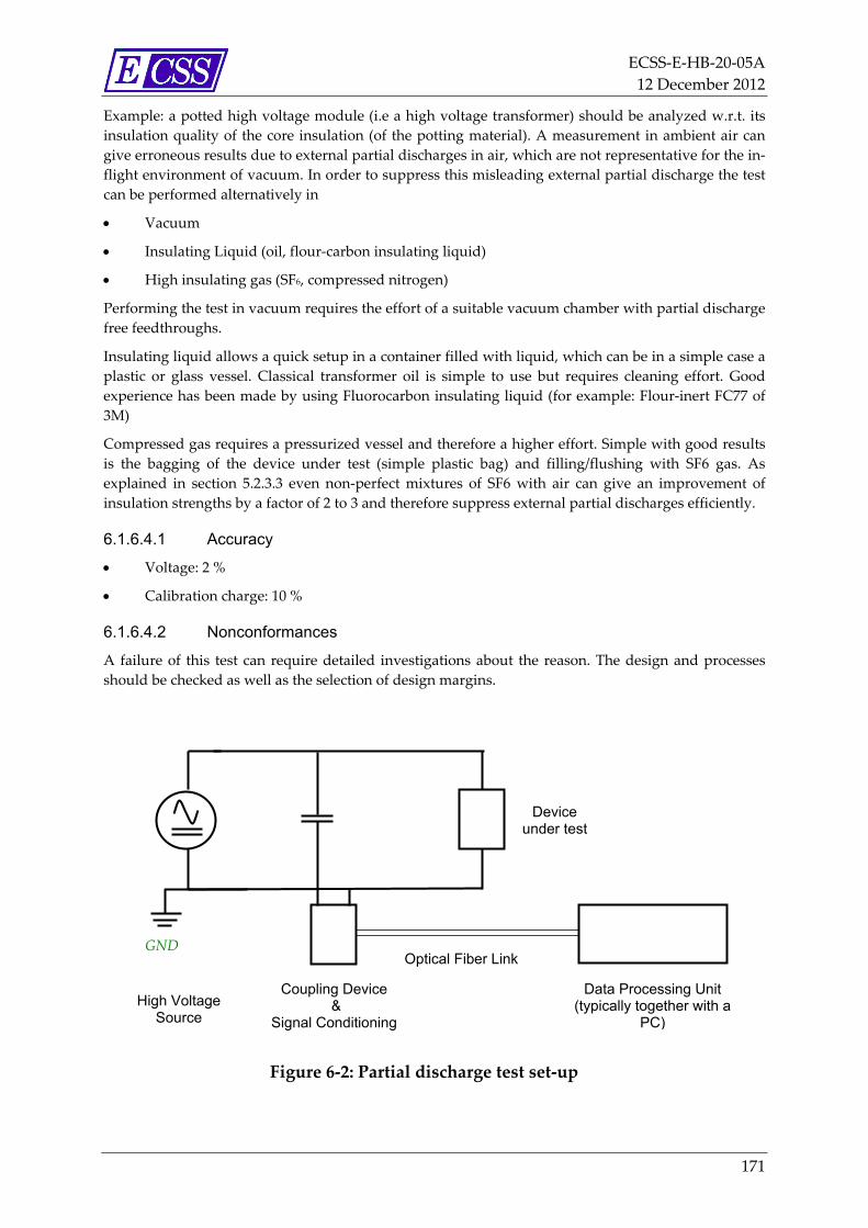
ECSS‐E‐HB‐20‐05A
12 December 2012
171
Example: a potted high voltage module (i.e a high voltage transformer) should be analyzed w.r.t. its
insulation quality of the core insulation (of the potting material). A measurement in ambient air can
give erroneous results due to external partial discharges in air, which are not representative for the in‐
flight environment of vacuum. In order to suppress this misleading external partial discharge the test
can be performed alternatively in
Vacuum
Insulating Liquid (oil, flour‐carbon insulating liquid)
High insulating gas (SF6, compressed nitrogen)
Performing the test in vacuum requires the effort of a suitable vacuum chamber with partial discharge
free feedthroughs.
Insulating liquid allows a quick setup in a container filled with liquid, which can be in a simple case a
plastic or glass vessel. Classical transformer oil is simple to use but requires cleaning effort. Good
experience has been made by using Fluorocarbon insulating liquid (for example: Flour‐inert FC77 of
3M)
Compressed gas requires a pressurized vessel and therefore a higher effort. Simple with good results
is the bagging of the device under test (simple plastic bag) and filling/flushing with SF6 gas. As
explained in section 5.2.3.3 even non‐perfect mixtures of SF6 with air can give an improvement of
insulation strengths by a factor of 2 to 3 and therefore suppress external partial discharges efficiently.
6.1.6.4.1 Accuracy
Voltage: 2 %
Calibration charge: 10 %
6.1.6.4.2 Nonconformances
A failure of this test can require detailed investigations about the reason. The design and processes
should be checked as well as the selection of design margins.
Figure 6‐2: Partial discharge test set‐up
GND
Coupling Device &
Signal Conditioning
Device under test
High Voltage Source
Optical Fiber Link
Data Processing Unit(typically together with a
PC)
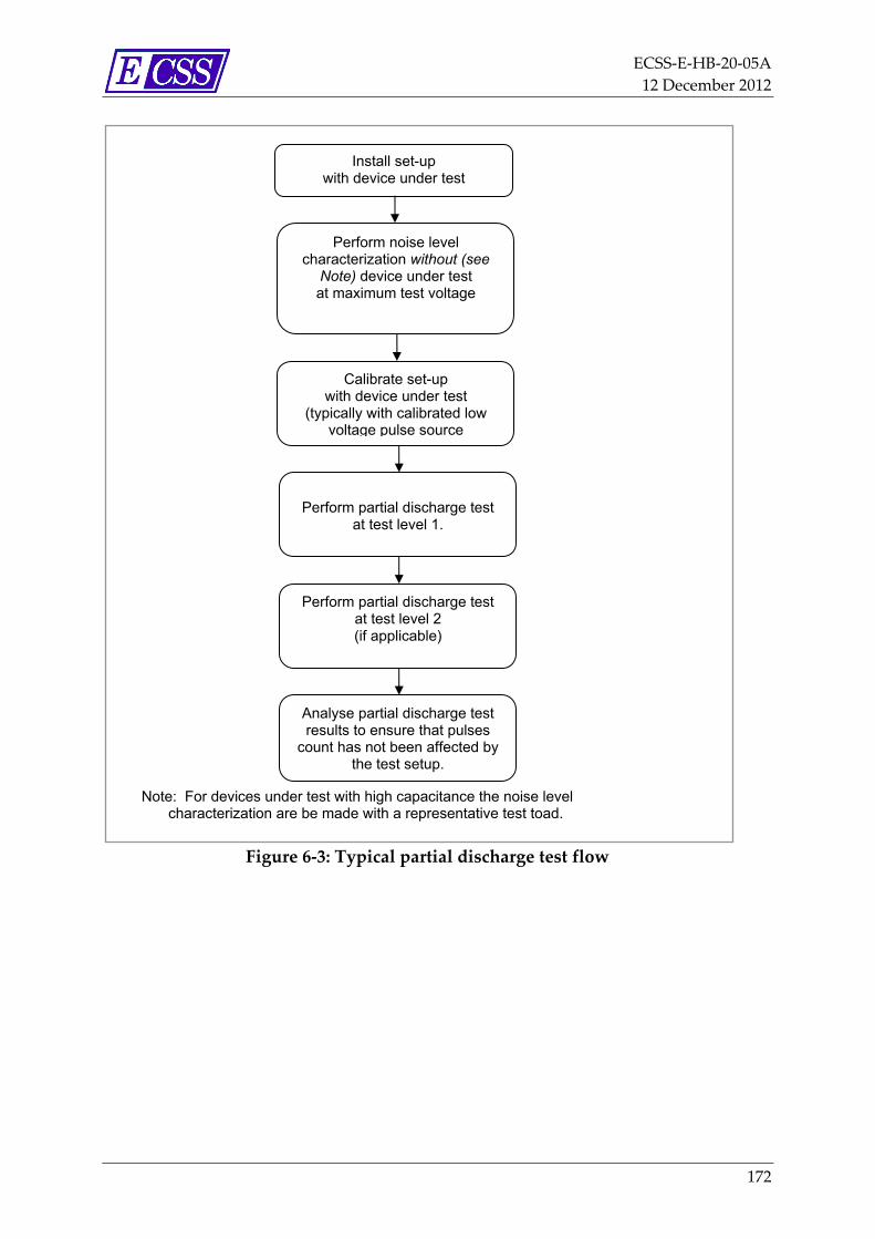
ECSS‐E‐HB‐20‐05A
12 December 2012
172
Figure 6‐3: Typical partial discharge test flow
Install set-up with device under test
Perform noise level characterization without (see
Note) device under test at maximum test voltage
Calibrate set-up with device under test
(typically with calibrated low voltage pulse source
Perform partial discharge test
at test level 1.
Perform partial discharge test at test level 2 (if applicable)
Note: For devices under test with high capacitance the noise level characterization are be made with a representative test toad.
Analyse partial discharge test results to ensure that pulses
count has not been affected by the test setup.
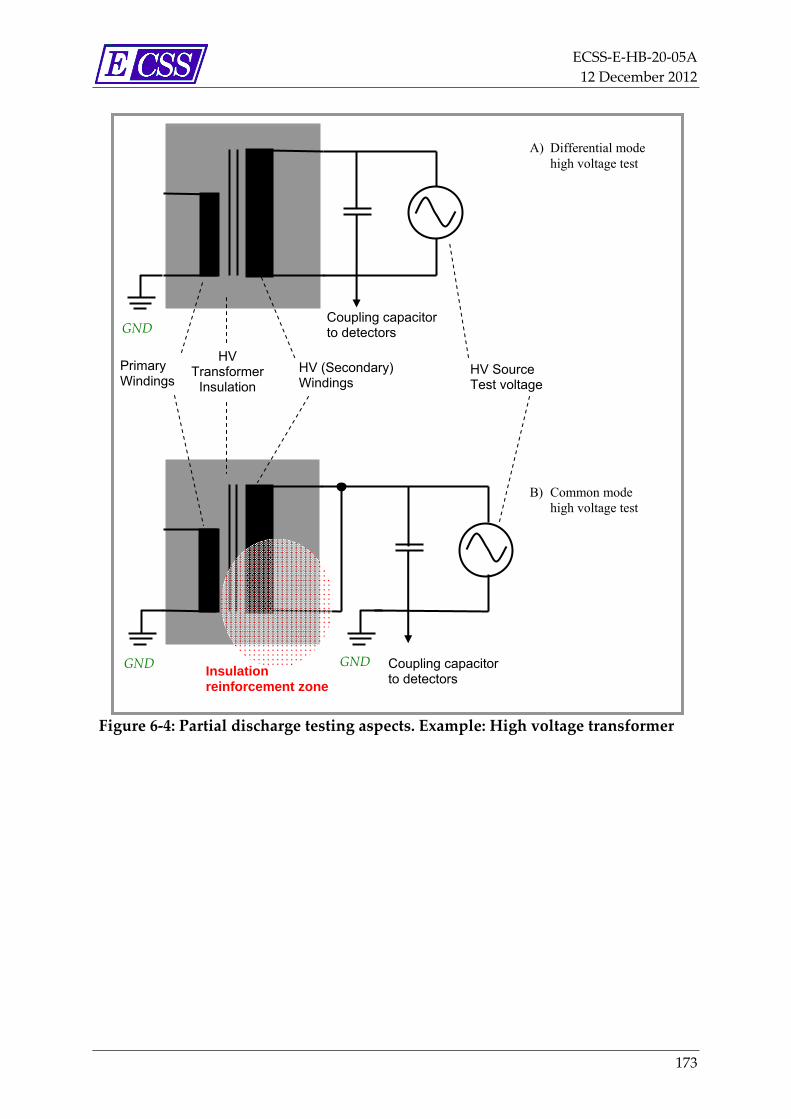
ECSS‐E‐HB‐20‐05A
12 December 2012
173
Figure 6‐4: Partial discharge testing aspects. Example: High voltage transformer
B) Common mode high voltage test
GND
Primary Windings
Coupling capacitor to detectors
HV (Secondary)Windings
Coupling capacitor to detectors
HV Transformer
Insulation
GND GND
HV Source Test voltage
A) Differential mode high voltage test
Insulation reinforcement zone
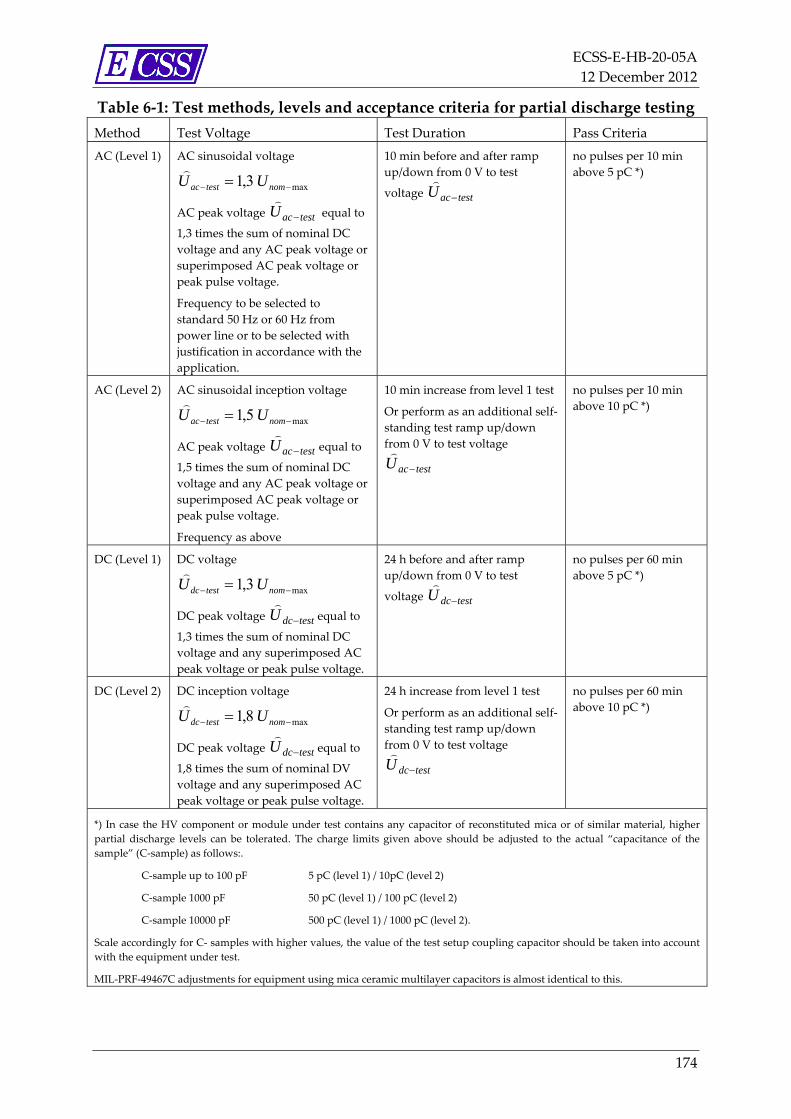
ECSS‐E‐HB‐20‐05A
12 December 2012
174
Table 6‐1: Test methods, levels and acceptance criteria for partial discharge testing
Method Test Voltage Test Duration Pass Criteria
AC (Level 1) AC sinusoidal voltage
max3,1 nomtestac UU
AC peak voltage testacU
equal to
1,3 times the sum of nominal DC
voltage and any AC peak voltage or
superimposed AC peak voltage or
peak pulse voltage.
Frequency to be selected to
standard 50 Hz or 60 Hz from
power line or to be selected with
justification in accordance with the
application.
10 min before and after ramp
up/down from 0 V to test
voltage testacU
no pulses per 10 min
above 5 pC *)
AC (Level 2) AC sinusoidal inception voltage
max5,1 nomtestac UU
AC peak voltage testacU
equal to
1,5 times the sum of nominal DC
voltage and any AC peak voltage or
superimposed AC peak voltage or
peak pulse voltage.
Frequency as above
10 min increase from level 1 test
Or perform as an additional self‐
standing test ramp up/down
from 0 V to test voltage
testacU
no pulses per 10 min
above 10 pC *)
DC (Level 1) DC voltage
max3,1 nomtestdc UU
DC peak voltage testdcU
equal to
1,3 times the sum of nominal DC
voltage and any superimposed AC
peak voltage or peak pulse voltage.
24 h before and after ramp
up/down from 0 V to test
voltage testdcU
no pulses per 60 min
above 5 pC *)
DC (Level 2) DC inception voltage
max8,1 nomtestdc UU
DC peak voltage testdcU
equal to
1,8 times the sum of nominal DV
voltage and any superimposed AC
peak voltage or peak pulse voltage.
24 h increase from level 1 test
Or perform as an additional self‐
standing test ramp up/down
from 0 V to test voltage
testdcU
no pulses per 60 min
above 10 pC *)
*) In case the HV component or module under test contains any capacitor of reconstituted mica or of similar material, higher
partial discharge levels can be tolerated. The charge limits given above should be adjusted to the actual “capacitance of the
sample” (C‐sample) as follows:.
C‐sample up to 100 pF 5 pC (level 1) / 10pC (level 2)
C‐sample 1000 pF 50 pC (level 1) / 100 pC (level 2)
C‐sample 10000 pF 500 pC (level 1) / 1000 pC (level 2).
Scale accordingly for C‐ samples with higher values, the value of the test setup coupling capacitor should be taken into account
with the equipment under test.
MIL‐PRF‐49467C adjustments for equipment using mica ceramic multilayer capacitors is almost identical to this.
ECSS‐E‐HB‐20‐05A
12 December 2012
175
6.1.7 Dielectric Withstanding Voltage Test (DWV)
6.1.7.1 Objective
High voltage tests are intended to detect insulation flaws, discontinuities, ageing cracks, and
deteriorated or weak insulation.
6.1.7.2 Rationale
Repeated application of high potential test voltages can reduce the dielectric strength and life of the
insulation. Any significant reduction in dielectric strength depends on the number of tests, the
insulation material, and the insulation thickness. Up to ten high‐potential tests can probably not
permanently damage the insulation.
6.1.7.3 Method
Proposed test conditions are:
Environment: to be selected in accordance with representative stress of the insulation
Duration: 60 s
Test Voltage: DC, AC, pulse: voltage testU :
for Level 2 test: nomtest UU 3 *)
for Level 1 test: nomtest UU 2 *)
where the nominal voltage nomU is maximum voltage of operation
*) The test level should be adjusted (lowered) carefully for hardware used later for flight, or
protoflight assemblies, if there is the danger that the high test voltage contributes to significant pre‐
aging or other applicable ratings of involved components are exceeded.
Level 2 testing is proposed to demonstrate design margin assuming that a high voltage device is
operated with a derating factor of 0,5 and tested at 1,5 times the rated voltage. Level 2 testing should
not be repeated too often as it can overstress the insulation. Therefore it is proposed for qualification
test and an initial test at acceptance. Repeated test on flight hardware should follow Level 1
conditions.
The voltage waveform should be selected according to the real application, so for DC operation a DC
voltage test should be selected.
A proposed electrical set‐up is shown in Figure 6‐5.
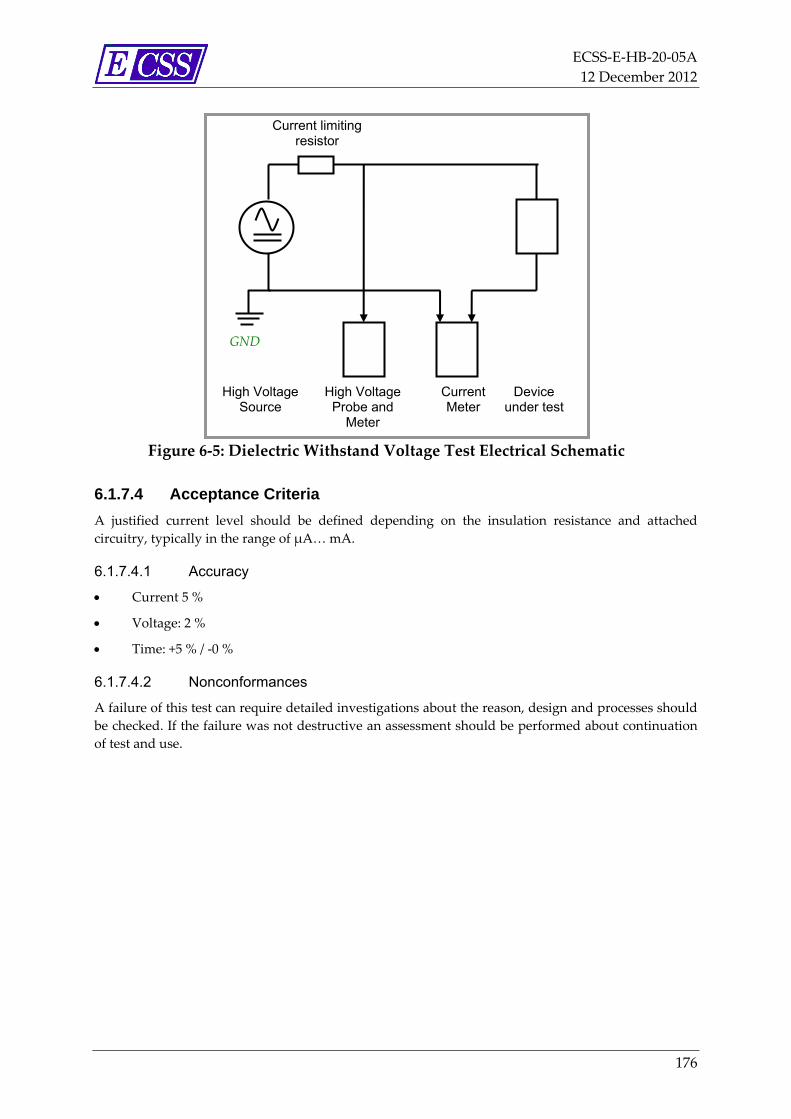
ECSS‐E‐HB‐20‐05A
12 December 2012
176
Figure 6‐5: Dielectric Withstand Voltage Test Electrical Schematic
6.1.7.4 Acceptance Criteria
A justified current level should be defined depending on the insulation resistance and attached
circuitry, typically in the range of μA… mA.
6.1.7.4.1 Accuracy
Current 5 %
Voltage: 2 %
Time: +5 % / ‐0 %
6.1.7.4.2 Nonconformances
A failure of this test can require detailed investigations about the reason, design and processes should
be checked. If the failure was not destructive an assessment should be performed about continuation
of test and use.
GND
Current limiting resistor
High Voltage Probe and
Meter
Device under test
High Voltage Source
Current Meter
ECSS‐E‐HB‐20‐05A
12 December 2012
177
6.1.8 Triple Junction Test (TRJ)
6.1.8.1 Applicability
This test is primarily dedicated to vacuum insulations in order to ensure that with applied high
voltage no leakage currents are present due to surface conductivity and electron emissions caused by
local electron emission sites present on surfaces, especially at sharp‐edged metallic structures and at
triple‐junction zones.
6.1.8.2 Objective
The test detects leakage currents due to degradation of vacuum insulation, when high voltage is
applied. It can detect problems due to design, processes and workmanship after assembly and
integration.
6.1.8.3 Rationale
The test should be applied at module and/or equipment level after initial insulation characterization,
however, it can be inserted or repeated in any test sequence or operational life cycle.
6.1.8.4 Method
This test is applicable to test for potential failure modes due to leakage currents in vacuum. Such
leakage currents often occur from emission sites on the surface of electrodes at locations with high
field strengths. Critical zones for emitters are the triple junction zones of electrical insulations as well
as sharp edged structures of the conductors. Contamination by gas layers, particles etc. promote this
effect. The effect is voltage and temperature dependence and can be time dependent as well.
The test is performed by applying a high voltage for a significant length to the device under test.
Proposed test conditions are:
Pressure: in Vacuum Chamber with pressures lower than 10‐4 mbar.
Temperature: at high level, equivalent to maximum operation temperature for acceptance or
qualification.
Duration: 36 hours
Test Voltage: DC voltage testU :
for Level 2 test: nomtest UU 2
for Level 1 test: nomtest UU
where the nominal voltage nomU is maximum voltage of operation
*) The test level should be adjusted (lowered) carefully for hardware used later for flight, or
protoflight assemblies, if there is the danger that the high test voltage contributes to significant pre‐
aging aging or other applicable ratings of involved components are exceeded.
Level 2 testing is proposed to demonstrate design margin on single “non‐sensitive” modules, for
example for simple insulators. Level 1 testing is proposed for assemblies of high voltage circuits or for
“sensitive” modules, for example modules including electronic components. Test level should be
adjusted, if justified by a suitable rationale.
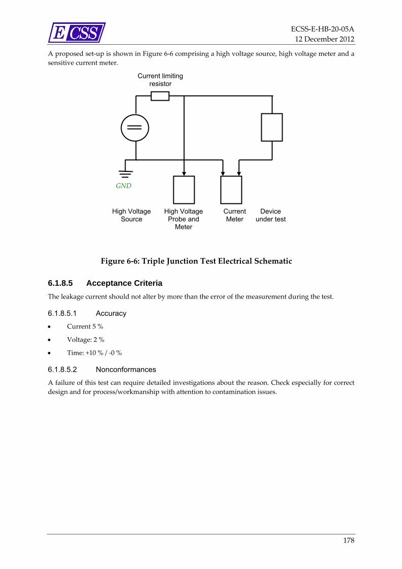
ECSS‐E‐HB‐20‐05A
12 December 2012
178
A proposed set‐up is shown in Figure 6‐6 comprising a high voltage source, high voltage meter and a
sensitive current meter.
Figure 6‐6: Triple Junction Test Electrical Schematic
6.1.8.5 Acceptance Criteria
The leakage current should not alter by more than the error of the measurement during the test.
6.1.8.5.1 Accuracy
Current 5 %
Voltage: 2 %
Time: +10 % / ‐0 %
6.1.8.5.2 Nonconformances
A failure of this test can require detailed investigations about the reason. Check especially for correct
design and for process/workmanship with attention to contamination issues.
GND
Current limiting resistor
High Voltage Probe and
Meter
Device under test
High Voltage Source
Current Meter
ECSS‐E‐HB‐20‐05A
12 December 2012
179
6.1.9 Critical pressure testing/Corona testing (CPT)
6.1.9.1 Objective
Critical pressure testing (often called: Corona Testing) is used to ensure, that a component, an
equipment or a subsystem can be safely operated at critical pressures according to the Paschen Curve
(see sections 4.3.4 and 5.1.8).
6.1.9.2 Rationale
There are different classes of items under test:
Class 1: For test items which are not fully encapsulated (high voltage conductors not exposed to
the vacuum) to demonstrate margin and/or safe operation.
In this case it should be taken care, that the electrical test environment, which is exposed to the
same low pressure environment as the item under test is safe for operation at low pressure.
Class 2: For test items which are fully encapsulated (high voltage conductors exposed to the
vacuum) to demonstrate margin and/or safe operation.
In this case the test requires completely encapsulated high voltage equipment operated in a
high voltage chamber. This includes all high voltage connections and set‐up used as a test
environment, too.
6.1.9.3 Method
Proposed test conditions are:
Test environment: Test performed in a vacuum chamber
Pressure:
starting pressure Paambientphigh510
end pressure Paambientplow210
Duration: Pressure variation (sweep) from highp to lowp within 10 min to 15 min.
Margin demonstration:
Design margin can be demonstrated either by voltage or pressure.
Test Voltage: DC, AC, pulse: voltage testU :
o for Level 2 test: nomtest UU 2 *)
o for Level 1 test: nomtest UU
where the nominal voltage nomU is maximum voltage of operation
NOTE *) for qualification the level of voltage should be carefully selected
according to the specific application.
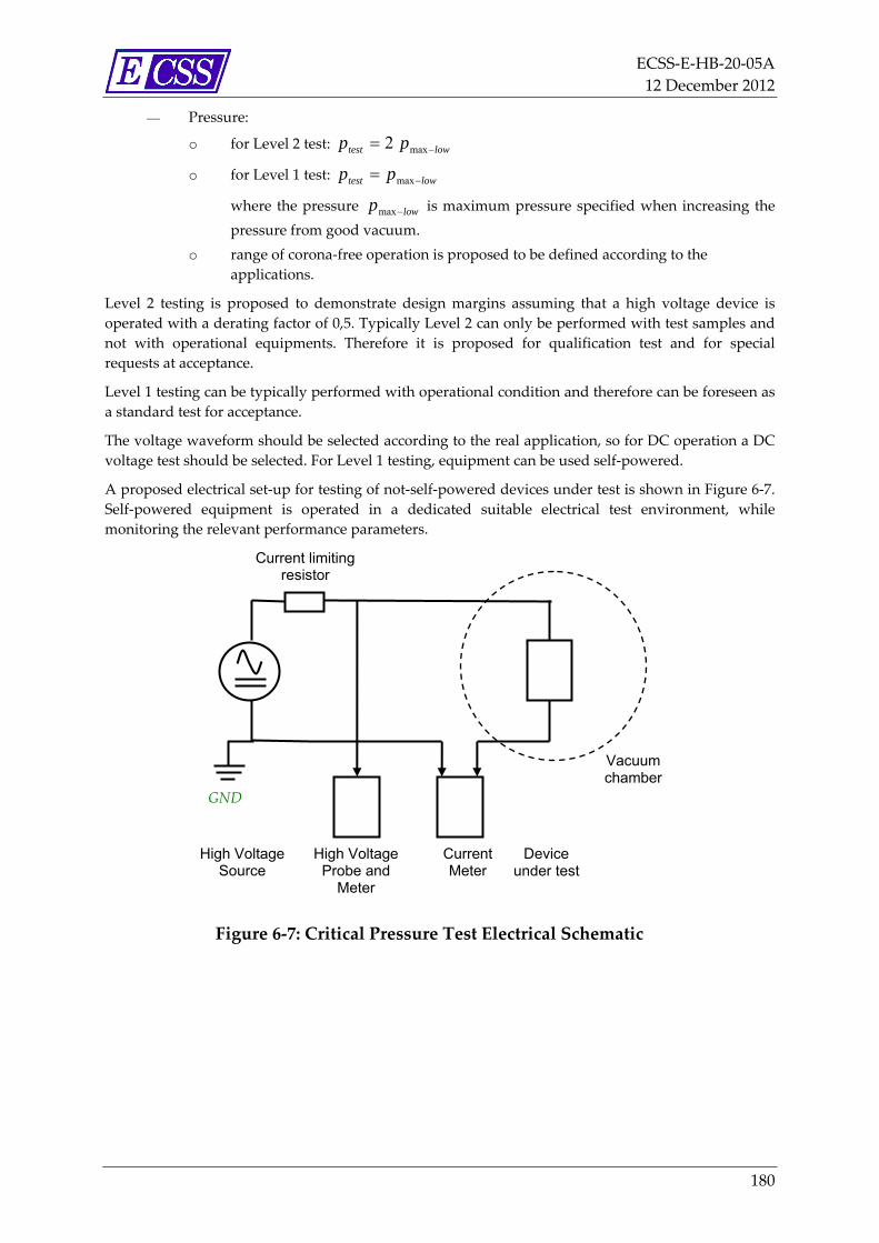
ECSS‐E‐HB‐20‐05A
12 December 2012
180
Pressure:
o for Level 2 test: lowtest pp max2
o for Level 1 test: lowtest pp max
where the pressure lowp max is maximum pressure specified when increasing the
pressure from good vacuum.
o range of corona‐free operation is proposed to be defined according to the
applications.
Level 2 testing is proposed to demonstrate design margins assuming that a high voltage device is
operated with a derating factor of 0,5. Typically Level 2 can only be performed with test samples and
not with operational equipments. Therefore it is proposed for qualification test and for special
requests at acceptance.
Level 1 testing can be typically performed with operational condition and therefore can be foreseen as
a standard test for acceptance.
The voltage waveform should be selected according to the real application, so for DC operation a DC
voltage test should be selected. For Level 1 testing, equipment can be used self‐powered.
A proposed electrical set‐up for testing of not‐self‐powered devices under test is shown in Figure 6‐7.
Self‐powered equipment is operated in a dedicated suitable electrical test environment, while
monitoring the relevant performance parameters.
Figure 6‐7: Critical Pressure Test Electrical Schematic
GND
Current limiting resistor
High Voltage Probe and
Meter
Device under test
High Voltage Source
Current Meter
Vacuum chamber
ECSS‐E‐HB‐20‐05A
12 December 2012
181
6.1.9.4 Acceptance Criteria
A self‐powered equipment should be checked against its performance criteria defined in the
applicable requirement specification and accuracy level selected suitable to that. For externally
powered devices under test the following acceptance criterion levels can be considered.
Leakage current should not increase during pressure sweep.
6.1.9.4.1 Accuracy
A self‐powered equipment should be checked against its performance criteria defined in the
applicable requirement specification and accuracy level selected suitable to that. For externally
powered devices under test the following accuracy levels can be considered.
Time: 5 %
Voltage: 2 %
Current: 3 %
6.1.9.4.2 Nonconformances
A failure of this test can require detailed investigations about the reason. The design and processes
should be checked as well as the selection of design margins.
ECSS‐E‐HB‐20‐05A
12 December 2012
182
6.1.10 Life testing (LIT)
6.1.10.1 Objective
Life testing should ensure that a high voltage equipment, module or component is capable to achieve
the specified lifetime requirements.
6.1.10.2 Rationale
Life testing is proposed to be performed for all new high voltage equipment, module or component to
be qualified. A strategy should be applied according to an evaluation plan to decide, on which level
(subsystem, equipment, module, component) needs to be performed, covering the maximum level of
stress from nominal operation.
6.1.10.3 Method
Proposed test conditions are:
Test environment: Selection in accordance with the nominal operational scenario of the device
under test. Simplifications – for example replacing thermal‐vacuum by thermal test in air – are
only proposed if well justified, i.e. if the representative environment is covered by another test
or if it can be demonstrated, that the replacement environment does not endanger the objectives
of the test.
Duration: Life time plus margin.
Remark: Duration can be adjusted to ensure adequate development cost and schedule. In this
case the can be only an adequate fraction of the operational mission time.
An often used duration for long term mission is: 1500 h.
Operating: Representative sequence of operating modes
Temperatures:
Qualification temperatures including temperature cycles and cold start
Measurement: Performance parameter according to specification. Monitor insulation current,
where necessary and/or where no performance parameter available.
6.1.10.4 Acceptance Criteria
No failure and no degradation of performance against specification considering the applicable drifts
including end of life.
6.1.10.4.1 Accuracy
Adequate accuracy is proposed to ensure measurement of performance parameters better than their
tolerances including drift and ageing.
6.1.10.4.2 Nonconformances
Complete failure like partial and full breakdown lead to fail of test. Untypical performance
degradation (out of spec measurements) requires detailed investigations about the reason. The design
and processes should be checked as well as the selection of design margins.
ECSS‐E‐HB‐20‐05A
12 December 2012
183
6.1.11 Accelerated life testing (ALT)
6.1.11.1 Objective
Accelerated life testing should ensure that a high voltage equipment, module or component is capable
to achieve the specified lifetime requirements.
6.1.11.2 Rationale
Accelerated life testing is proposed to be performed for all new high voltage equipment, module or
component to be qualified. A strategy should be applied according to an evaluation plan to decide, on
which level (subsystem, equipment, module, component) needs to be performed, covering the
maximum level of stress from nominal operation. An acceleration factor is defined in accordance with
an applicable stress lifetime law (see section 4.3.5 ‐ Ageing).
As the accelerated life test often requires increase of operating conditions (voltage, temperatures, etc.)
beyond the nominal settings of equipment, it is often proposed to perform the accelerated life test on
module or component level, if well justified.
6.1.11.3 Method
Proposed test conditions are:
Test environment: Selection in accordance with the nominal operational scenario of the device
under test. Simplifications – for example replacing thermal‐vacuum by thermal test in air – are
only proposed if well justified, i.e. if the representative environment is covered by another test
or if it can be demonstrated, that the replacement environment does not endanger the
objectives of the test.
Duration: Adequate according to applicable stress‐lifetime law.
In the case the stress‐lifetime relation is not known or confirmed, an evaluation program for
identification of the stress‐lifetime curve should be performed in advance.
Operating: According to stress life time law.
Temperatures: According to stress life time law.
Measurement: Performance parameter according to specification. Insulation current, where
necessary and/or where no performance parameter available.
6.1.11.4 Acceptance Criteria
No failure and no degradation of performance against specification considering the applicable drifts
including end of life.
6.1.11.4.1 Accuracy
Adequate accuracy is proposed to ensure measurement of performance parameters better than their
tolerances including drift and ageing.
6.1.11.4.2 Nonconformances
Complete failure like partial and full breakdown lead to fail of test. Untypical performance
degradation (out of spec measurements) requires detailed investigations about the reason. The design
and processes should be checked as well as the selection of design margins.

ECSS‐E‐HB‐20‐05A
12 December 2012
184
6.1.12 Burn-in testing (BIT)
6.1.12.1 Objective
Burn‐in testing should ensure that a high voltage equipment, module or component is not subject of
so‐called “infant mortality”.
6.1.12.2 Rationale
Burn‐in testing is proposed to be performed for all high voltage equipment, module or component to
be delivered as flight hardware. A strategy should be applied according to an evaluation plan to
decide, on which level (subsystem, equipment, module, component) needs to be performed, covering
the maximum level of stress from nominal operation without reducing the expected lifetime
significantly.
6.1.12.3 Method
Proposed test conditions are:
Test environment: Selection in accordance with the nominal operational scenario of the device
under test. Simplifications – for example replacing thermal‐vacuum by thermal test in air – are
only proposed if well justified, i.e. if the representative environment is covered by another test
or if it can be demonstrated, that the replacement environment does not endanger the objectives
of the test.
Duration: A negligible fraction of life time ensuring to address “infant mortality” sufficiently.
An often used duration for long term missions is: 100 h and/or 3 full temperature cycles
according to acceptance level.
Operating: Representative sequence of operating modes
Temperatures: Acceptance temperatures including temperature cycles and cold start
Measurement: Performance parameter according to specification. Insulation current, where
necessary and/or where no performance parameter available.
6.1.12.4 Acceptance Criteria
No failure and no degradation of performance against specification considering the applicable drifts
including end of life.
6.1.12.4.1 Accuracy
Adequate accuracy is proposed to ensure measurement of performance parameters better than their
tolerances including drift and ageing.
6.1.12.4.2 Nonconformances
Complete failure like partial or full breakdown lead to fail of test. Untypical performance degradation
(out of spec measurements) requires detailed investigations about the reason. The design and
processes should be checked as well as the selection of design margins.
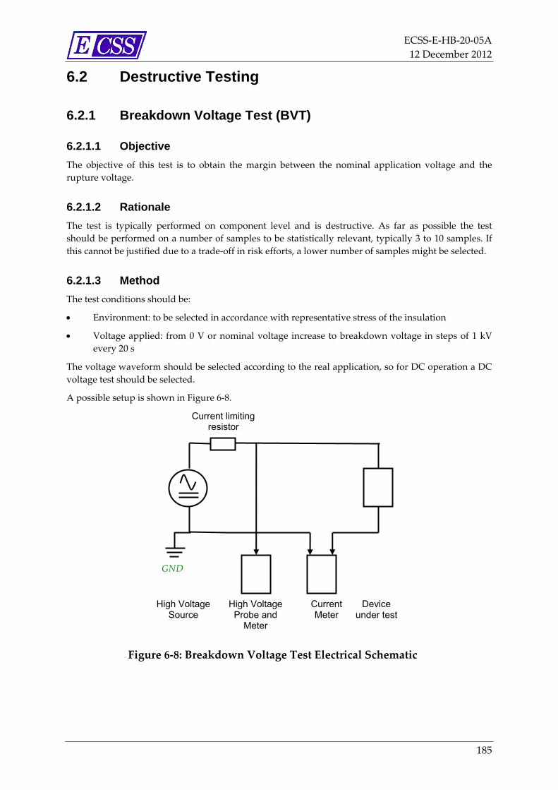
ECSS‐E‐HB‐20‐05A
12 December 2012
185
6.2 Destructive Testing
6.2.1 Breakdown Voltage Test (BVT)
6.2.1.1 Objective
The objective of this test is to obtain the margin between the nominal application voltage and the
rupture voltage.
6.2.1.2 Rationale
The test is typically performed on component level and is destructive. As far as possible the test
should be performed on a number of samples to be statistically relevant, typically 3 to 10 samples. If
this cannot be justified due to a trade‐off in risk efforts, a lower number of samples might be selected.
6.2.1.3 Method
The test conditions should be:
Environment: to be selected in accordance with representative stress of the insulation
Voltage applied: from 0 V or nominal voltage increase to breakdown voltage in steps of 1 kV
every 20 s
The voltage waveform should be selected according to the real application, so for DC operation a DC
voltage test should be selected.
A possible setup is shown in Figure 6‐8.
Figure 6‐8: Breakdown Voltage Test Electrical Schematic
GND
Current limiting resistor
High Voltage Probe and
Meter
Device under test
High Voltage Source
Current Meter
ECSS‐E‐HB‐20‐05A
12 December 2012
186
6.2.1.4 Acceptance Criteria
A design margin should be adequately defined in view of the tested component/material.
6.2.1.4.1 Accuracy
Voltage: 2 %
6.2.1.4.2 Nonconformances
A failure of this test can require detailed investigations about the reason. The design and processes
should be checked as well as the selection of design margins.
6.2.2 Lifetime evaluation testing (LET)
6.2.2.1 Objective
Evaluation of a stress life‐lifetime relation in order to predict lifetime of a high voltage device.
6.2.2.2 Rationale
A suitable number of samples need to be tested under different stress conditions to determine a stress‐
lifetime law. Possible relations are described in section 4.3.5. A strategy should be applied according
to an evaluation plan to decide, which stress parameters are evaluated and which type of samples
(design) and which number of samples should be tested at various stress level until loss of insulation
or relevant function.
6.2.2.3 Method
Proposed test conditions are:
Test environment: Selection in accordance with the nominal operational scenario of the device
under test. Simplifications – for example replacing thermal‐vacuum by thermal test in air – are
only proposed if well justified, i.e. if the representative environment is covered by another test
or if it can be demonstrated that the replacement environments does not endanger the
objectives of the test.
Duration: Adequate according to applicable stress‐lifetime law.
In case the stress‐lifetime relation is not known or confirmed, an evaluation program for
identification of the stress‐lifetime curve should be performed in advance.
Operating: According to stress life time law.
Temperatures: According to stress life time law.
Measurement: Performance parameter according to specification. Insulation current, where
necessary and/or where no performance parameter available.
6.2.2.4 Acceptance Criteria
Not applicable.
6.2.2.4.1 Accuracy
Adequate accuracy is proposed to ensure measurement of performance parameters better than their
tolerances including drift and ageing.
ECSS‐E‐HB‐20‐05A
12 December 2012
187
6.2.2.4.2 Nonconformances
Not applicable.
6.3 Supplementary Methods There are several methods to support high voltage testing and/or to ensure a proper quality of
insulation.
a. Ultrasonic Scanning
Ultrasonic scanning allows detection of voids or cracks inside insulation, especially for small
and thin items.
b. X‐Ray Scanning
X‐Ray scanning allows detection of voids or cracks inside insulation and is useful for bulky
items. Evaluation becomes more difficult with multiple layers of components and with complex
metal parts like transformer windings.
c. Visual Inspection
Visual inspection is a standard measure before and after test to identify visible defects and
contaminations.
d. Audible Detection
Audible detection is useful to identify partial discharges especially on the outside of conductors
and HV assemblies, which are not fully encapsulated. It is useful as well to identify unwanted
discharges in a test environment/test set‐up.
e. Visible Detection
Visible detection is useful to identify partial discharges especially on the outside of conductors
and HV assemblies, which are not fully encapsulated. It is useful as well to identify unwanted
discharges in test environment/test set‐up. Visible detection requires typically a dark room or
chamber.
f. Chemical Analysis
Chemical analysis can be useful to ensure the quality of a liquid or gaseous insulation. The
initial status before use and changes after testing or operation can be stated and compared to a
reference.

ECSS‐E‐HB‐20‐05A
12 December 2012
188
6.4 Testing strategy An adequate testing strategy should be selected depending on the application and on the scope of the
test campaign. The following table provides an assessment of the various test methods and a
recommendation, where to apply:
Table 6‐2: Assessment of test methods w.r.t. its application
Test method Item under test Apply for
Insulation Resistance Test
(INR)
Samples
Subassemblies
Assemblies, Units
Material Selection
Process Evaluation & Validation
Qualification Testing of Items
Acceptance of Testing of Items
Bulk Resistance Measurement
(BRM)
Samples
Material Selection
Process Evaluation & Validation
Surface Resistance
Measurement (SRM)
Samples
Material Selection
Process Evaluation & Validation
Dielectric Loss Factor Test
(DLF)
Samples
Subassemblies
Material Selection
Process Evaluation & Validation
Polarisation and
Depolarisation Current
Measurement (PDC)
Samples
Subassemblies
Material Selection
Process Evaluation & Validation
Partial Discharge Test (PDT) Samples
Subassemblies
Assemblies,
Material Selection
Process Evaluation & Validation
Qualification Testing of Items
Acceptance of Testing of Items
Dielectric Withstanding
Voltage Test (DWV)
Samples
Subassemblies
Assemblies
Material Selection
Process Evaluation & Validation
Qualification Testing of Items
Acceptance of Testing of Items
Triple Junction Test (TRJ) Subassemblies
Assemblies,
Units
Only for items in vacuum with non‐
encapsulated high voltages:
Process Evaluation & Validation
Qualification Testing of Items
Acceptance of Testing of Items
Critical pressure
testing/Corona testing (CPT)
Subassemblies
Assemblies,
Units
Process Evaluation & Validation
Qualification Testing of Items
Acceptance of Testing of Items
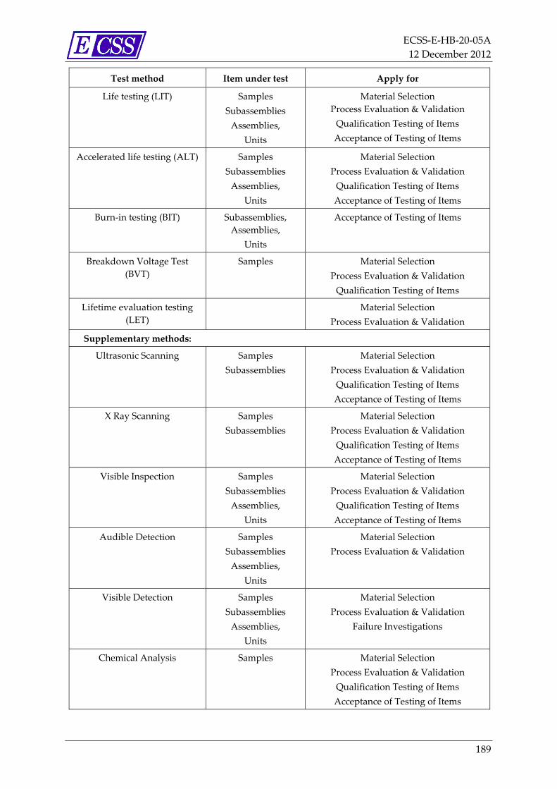
ECSS‐E‐HB‐20‐05A
12 December 2012
189
Test method Item under test Apply for
Life testing (LIT) Samples
Subassemblies
Assemblies,
Units
Material Selection
Process Evaluation & Validation
Qualification Testing of Items
Acceptance of Testing of Items
Accelerated life testing (ALT) Samples
Subassemblies
Assemblies,
Units
Material Selection
Process Evaluation & Validation
Qualification Testing of Items
Acceptance of Testing of Items
Burn‐in testing (BIT) Subassemblies,
Assemblies,
Units
Acceptance of Testing of Items
Breakdown Voltage Test
(BVT)
Samples Material Selection
Process Evaluation & Validation
Qualification Testing of Items
Lifetime evaluation testing
(LET)
Material Selection
Process Evaluation & Validation
Supplementary methods:
Ultrasonic Scanning Samples
Subassemblies
Material Selection
Process Evaluation & Validation
Qualification Testing of Items
Acceptance of Testing of Items
X Ray Scanning Samples
Subassemblies
Material Selection
Process Evaluation & Validation
Qualification Testing of Items
Acceptance of Testing of Items
Visible Inspection Samples
Subassemblies
Assemblies,
Units
Material Selection
Process Evaluation & Validation
Qualification Testing of Items
Acceptance of Testing of Items
Audible Detection Samples
Subassemblies
Assemblies,
Units
Material Selection
Process Evaluation & Validation
Visible Detection Samples
Subassemblies
Assemblies,
Units
Material Selection
Process Evaluation & Validation
Failure Investigations
Chemical Analysis Samples Material Selection
Process Evaluation & Validation
Qualification Testing of Items
Acceptance of Testing of Items
ECSS‐E‐HB‐20‐05A
12 December 2012
190
7 High voltage product aspects
7.1.1 Best practice for materials and processes selection It is proposed that materials selected for high voltage insulations dedicated to qualification and to
flight products is performed in accordance with the following criteria:
High electric strengths
A good material should allow continuous operation with field strengths higher than 6 kV/mm
over lifetime for DC applications and higher than 2 kV/mm for AC applications. Short‐term
breakdown strengths (typical material data sheet values) should not be lower than 20 kV/mm
Low dielectric losses (high insulation resistance, low loss factor for AC applications)
Low degradation over lifetime
Free of partial discharges and/or resistant against partial discharge (low degradation)
The material itself or the process of manufacturing / application of the material needs to ensure
insulation without cracks, voids, gas bubbles, and delamination
Radiation resistance
Compatible with temperature range of use (including qualification)
Compatible with space environment including radiation
Table 7‐1 provides an overview of material properties, standard test methods and typical minimum
requirements to be considered for selection of materials.
It is proposed to perform selection under the following aspects:
Material selection based on ranking of properties
Process for procurement of the material (requirements, incoming inspections)
Process to produce the material (for self produced material, for example by potting process)
Process for use of the materials (treatments, cleanings)
As a guideline the following reference can be used:
Annex B.1: High Voltage Evaluation Plan
Annex B.2: Materials Evaluation
Annex B.3: PID – Process Identification Document

ECSS‐E‐HB‐20‐05A
12 December 2012
191
Table 7‐1: Typical material properties and reference test methods for high
voltage insulation materials
Properties Applicable
for
G=Gases
L=Liquids
S=Solids
Minimum Requirements
and
Applicability
Method Standard
General ‐ ‐
Heritage all ‐
Appearance L,S ‐
Number of Components S For composite materials ‐
Kind of Filler S For composite materials ‐
Physical Data
Outgassing Data S Fulfil ECSS‐Q‐70‐71A
Density (g/cm³) all Low ASTM‐D‐2240
Elastic Modulus (MPa)
‐35 °C ‐ +150 °C
S ASTM‐D‐695
Shore Hardness
At room temperature
S ASTM‐D‐2240
Tensile Strength (MPa)
at room temperature
S ASTM‐D‐638
Thermal Conductivity (W/m K)
At room temperature
all ASTM‐D‐2214
Glass Transition Temperature
(°C)
S For potting materials: should
be higher than max
operation temperature
ASTM E831 ‐ 06
Thermal Expansion (10‐6/K) S ASTM E831 ‐ 06
Radiation Resistance all Depending on mission
requirement
Service Temperature (°C) all High ASTM‐D‐794
Electrical Data
Dielectric Constant
50Hz
1kHz
1MHz
all Low ASTM‐D‐150
Dissipation Factor
50Hz
1kHz
1MHz
all Low ASTM‐D‐150
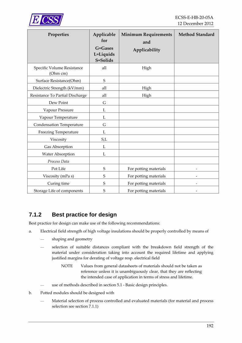
ECSS‐E‐HB‐20‐05A
12 December 2012
192
Properties Applicable
for
G=Gases
L=Liquids
S=Solids
Minimum Requirements
and
Applicability
Method Standard
Specific Volume Resistance
(Ohm cm)
all High
Surface Resistance(Ohm) S
Dielectric Strength (kV/mm) all High
Resistance To Partial Discharge all High
Dew Point G
Vapour Pressure L
Vapour Temperature L
Condensation Temperature G
Freezing Temperature L
Viscosity S,L
Gas Absorption L
Water Absorption L
Process Data
Pot Life S For potting materials ‐
Viscosity (mPa s) S For potting materials ‐
Curing time S For potting materials ‐
Storage Life of components S For potting materials ‐
7.1.2 Best practice for design
Best practice for design can make use of the following recommendations:
a. Electrical field strength of high voltage insulations should be properly controlled by means of
shaping and geometry
selection of suitable distances compliant with the breakdown field strength of the
material under consideration taking into account the required lifetime and applying
justified margins for derating of voltage resp. electrical field
NOTE Values from general datasheets of materials should not be taken as
reference unless it is unambiguously clear, that they are reflecting
the intended case of application in terms of stress and lifetime.
use of methods described in section 5.1 ‐ Basic design principles.
b. Potted modules should be designed with
Material selection of process controlled and evaluated materials (for material and process
selection see section 7.1.1)
ECSS‐E‐HB‐20‐05A
12 December 2012
193
It is preferred to base maximum permitted electrical field strengths and maximum
permitted average field strength on detailed life test evaluation. If these are not available
the following general rules can be applied:
Maximum permitted electrical field strengths
o for DC voltages: 6 kV/mm
o for AC voltages: 2 kV/mm
to be applied for qualified materials like epoxy, polyurethane and silicone.
Exceeding of these design values can be accepted if justified by sufficient evaluation
including adequate life testing and/or heritage of the process owner. The process needs to
be clearly identified by a PID (see section 7.1.1).
Lower limits can be applicable, if the selected material is obviously not capable to be
compliant with such stress under consideration of applicable lifetime requirement and/or
the process is not controlled.
If the process control is limited, the following maximum permitted electrical field
strengths should be applied
o for DC voltages: 2 kV/mm
o for AC voltages: 700 V/mm
c. Electrical field across surfaces in ambient air or high quality vacuum
a maximum permitted electrical field strengths are
o for DC voltages: 600 V/mm
o for AC voltages: 200 V/mm
Exceeding these design values can be accepted if justified by sufficient evaluation
including adequate life testing and/or heritage of the process owner. Improvements can
be achieved by suitable shaping of the insulator surface (see section 5.1.10). The process
of manufacturing needs to be clearly identified by a PID (see section 7.1.1).
Lower limits can be applicable, if the selected material is obviously not capable to be
compliant with such stress under consideration of applicable lifetime requirement and/or
the process is not controlled.
d. High voltage and low voltage electronic circuits should be separated sufficiently by means of
galvanic isolation
spacing
electrostatic shield
overvoltage suppression at critical inputs of sensitive low voltage circuits
e. High voltage circuits sensitive to critical pressure conditions (i.e. vented modules with non‐
encapsulated high voltage lines) should be designed in accordance with the following rules:
The worst case pressure should be assessed, taking into account the outgassing rates and
quantities of the materials used and the flow restriction of the openings of shields and
insulators for a molecular stream.
The electrode distance should be selected in accordance with the Paschen law.
For all applicable pressure conditions during operation the electrode separation should
be selected to ensure a design margin of factor 2, which means the design should
withstand two times the nominal maximum operating voltage.
ECSS‐E‐HB‐20‐05A
12 December 2012
194
Venting hole size of enclosing structures should be selected to >2 cm2 per 1000 cm3 of
enclosed volume, if no detailed venting analysis is performed.
Where applicable, attention should be paid to the venting hole size as well as the
maximum individual hole size, so that radiation does not enter into the equipment and
jeopardizes the functionality of the equipment, due to radiated susceptibility (RS) aspects.
This is particularly important when EP (electrical propulsion) is used on the spacecraft.”
f. High voltage connectors should not be used in harnesses exposed to critical low pressure or
vacuum unless they are qualified for this purpose.
g. For high voltage insulation made of potting materials the glass transition point should be
outside of the applicable (qualification) temperature range or instead it should be confirmed,
that the change of physical properties across this transitions is compatible with the selected
design.
h. High voltage wires should be used under the following aspects.
The maximum voltage applied should be 50 % of the manufacturerʹs rating. The
maximum AC voltage should be 5 % of the DC rating if not otherwise specified by the
manufacturer.
The minimum bend radius should be 5 times the manufacturer’s recommendation for
PTFE insulated wires and equal to the manufacturerʹs rating for other types.
Unshielded high voltage cables should not be routed near any sharp edges to avoid local
field concentration.
Splices should not degrade the voltage withstanding characteristics of the assembly
below the rating of the cable.
High voltage cable bundles which are not field controlled should operate partial
discharge free in vacuum, i.e. the sheath should allow adequate venting of the outgassing
products.
7.1.3 Best practice for qualification Note: under cover of this headline “qualification”, the specific needs for qualification to high voltage
technological items are addressed; general rules for qualification are given in ECSS‐E‐ST‐10‐03C.
Best practice for qualification should be distinguished between part/components and module,
assemblies, for example.
For parts and components qualification should follow the relevant ECSS, ESCC and MIL Specification
for HiRel space parts/components. Where these are not specific to high voltage at test the following
elements should be added:
a. Analysis of the electrical field and voltage stress.
Calculation of maximum electrical stress
Verification of suitability of design and materials with respect to electrical stress, in
specific
o demonstration of design margins (see section 7.1.2)
o assessment of lifetime.
b. Demonstration of margins by test for dielectric withstanding voltage (see section 6.1.7) with a
factor of 2 against maximum nominal operating voltage (including ripple and transients).
ECSS‐E‐HB‐20‐05A
12 December 2012
195
c. Partial discharge test (see section 6.1.6).
d. Life test (according to section 6.1.10.
For high voltage modules, assemblies and equipments the qualification should include:
e. Presentation of a high voltage evaluation plan according to section 7.1.7.
f. Documentation of all processes relevant for ensuring the quality of the high voltage insulation
by individual Process Identification Documents (PID) according to section 7.1.6.
g. Analysis of the electrical field and voltage stress.
Calculation of maximum electrical stress
Verification of suitability of design and materials with respect to electrical stress, in
specific
o demonstration of design margins (see section 7.1.2)
o assessment of lifetime.
h. Testing under consideration of the following sequence:
1. functional test
2. vibration
3. functional test
4. cold storage in air ‐ 24 hours
5. hot storage in vacuum ‐ 250 hours
6. functional test
7. thermal‐vacuum test (see section Life testing (LIT) 6.1.10)
8. functional test.
i. Thermal vacuum test sequence performed under h) with the following elements:
The thermal‐vacuum test should have a minimum duration of 1500 hours and consist of a
minimum of 100 cycles. The cycles should have a full temperature excursion between
qualification operating limits with hot operation at the maximum qualification
temperature during the remaining time.
The cycling should go on continuously with a maximum rate of change of 1
degree/minute and a minimum stabilisation time of 2 hours at temperature extremes. The
stabilisation time can be adapted to the real time constants of the item under test, if
useful.
Ten cold starts at the cold start temperature should be included at regular intervals in the
cycling sequence with 2 hours prior stabilisation times in cold storage condition.
For the first and the last test cycle the pressure should be deliberately raised to 10‐3 mbar,
in order to verify a margin of one decade, assuming worst case satellite pressure of 10‐4
mbar.
The above mentioned definition of number of cycles assumes that the item under test
experiences only a few full temperature cycles in its operational life (reference
geostationary telecom satellite with 15 years mission duration). The number of test cycles
should be increased if the specified number of operational cycles is higher.
The above mentioned definition of number of cycles and total test duration can be
reduced, if well justified for missions of very short durations.
The thermal –vacuum test can be replaced by a thermal test, if well justified that the
vacuum environment is not relevant for this test (for example: if the operating
environment is not vacuum).

ECSS‐E‐HB‐20‐05A
12 December 2012
196
7.1.4 Best practice for flight acceptance Best practice for flight acceptance should be distinguished between part/components and module,
assemblies etc.
For parts and components acceptance should follow the relevant ECSS, ESCC and MIL Specification
for HiRel space parts/components. Where these are not specific to high voltage at test the following
elements should be added:
a. Partial discharge test (see section 6.1.6).
b. Burn‐in test (according to section 6.1.12).
For high voltage modules, assemblies and equipments the acceptance should include:
c. Traceability that all process relevant for ensuring the quality of the high voltage insulation have
been performed in accordance with individual Process Identification Documents (PID)
according to section 7.1.3.
d. Testing under consideration of the following sequence:
1. functional test
2. vibration
3. functional test
4. cold storage in air ‐ 24 hours
5. hot operation in vacuum ‐ 250 hours
6. functional test
7. thermal‐vacuum test (see ECSS‐E‐ST‐10‐03 or any customer requirement)
8. functional test.
e. Thermal vacuum test sequence performed under c) with the following elements:
1. The thermal‐vacuum test should have a minimum duration of 250 h and consist of a
minimum of 10 cycles. The cycles have a full temperature excursion between acceptance
operating limits with hot operation at the maximum acceptance temperature during the
remaining time.
2. The cycling should go on continuously with a maximum rate of change of 1
degree/minute and a minimum stabilisation time of 2 hours at temperature extremes.
3. One cold starts at the cold start temperature should be included at regular intervals in the
cycling sequence with 2 hours prior stabilisation times in cold storage condition.
4. For the first and the last test cycle the pressure should be deliberately raised to 10‐3 mbar,
in order to verify a margin of one decade, assuming worst case satellite pressure of 10‐4
mbar.
5. The above mentioned definition of number cycles assumes that the item under test
experiences only a few full temperature cycles in its operational life (reference
geostationary telecom satellite with 15 years mission duration). The number of test cycles
should all be increased if the specified number of operational cycles is higher.
6. The above mentioned definition of number of cycles and total test duration can be
reduced, if well justified for missions of very short durations.
NOTE The thermal –vacuum test can be replaced by a thermal test, if well
justified that the vacuum environment is not relevant for this test
(for example: if the operating environment is not vacuum).
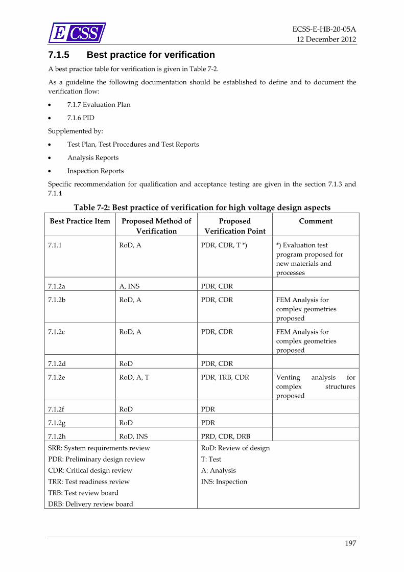
ECSS‐E‐HB‐20‐05A
12 December 2012
197
7.1.5 Best practice for verification A best practice table for verification is given in Table 7‐2.
As a guideline the following documentation should be established to define and to document the
verification flow:
7.1.7 Evaluation Plan
7.1.6 PID
Supplemented by:
Test Plan, Test Procedures and Test Reports
Analysis Reports
Inspection Reports
Specific recommendation for qualification and acceptance testing are given in the section 7.1.3 and
7.1.4
Table 7‐2: Best practice of verification for high voltage design aspects
Best Practice Item Proposed Method of
Verification
Proposed
Verification Point
Comment
7.1.1 RoD, A PDR, CDR, T *) *) Evaluation test
program proposed for
new materials and
processes
7.1.2a A, INS PDR, CDR
7.1.2b RoD, A PDR, CDR FEM Analysis for
complex geometries
proposed
7.1.2c RoD, A PDR, CDR FEM Analysis for
complex geometries
proposed
7.1.2d RoD PDR, CDR
7.1.2e RoD, A, T PDR, TRB, CDR Venting analysis for
complex structures
proposed
7.1.2f RoD PDR
7.1.2g RoD PDR
7.1.2h RoD, INS PRD, CDR, DRB
SRR: System requirements review
PDR: Preliminary design review
CDR: Critical design review
TRR: Test readiness review
TRB: Test review board
DRB: Delivery review board
RoD: Review of design
T: Test
A: Analysis
INS: Inspection
ECSS‐E‐HB‐20‐05A
12 December 2012
198
7.1.6 PID Processes used to manufacture qualified flight high voltage equipments and modules should be
documented and authorized through a dedicated Process Identification Document (PID)
Requirements. Each individual process should be covered by an individual PID. An example for the
content of a PID is given in Annex B.3. Change of the qualified process w.r.t the PID typically leads to
a re‐qualification.
7.1.7 Evaluation Plan An Evaluation Plan should be produced, planning the thorough investigation and characterisation of
the technologies and materials proposed for integration into HV equipments. For each technology a
categorisation should be used to determine, based on existing heritage if any, the work that should be
performed. An example for the content and scope of an Evaluation Plan is given in Annex B.1.
ECSS‐E‐HB‐20‐05A
12 December 2012
199
8 Specific problem areas
8.1.1 High voltage converters The typical problems of high voltage converters are related to
EMC issues (see section 8.1.5)
Flashover (in open circuit)
Effects related to critical pressure (Paschen breakdown)
In general it is proposed to a have a clear galvanic insulation between primary and secondary voltages
of a power conditioner which means galvanic insulation though a transformer in the power path. It is
furthermore valuable to have an electrostatic shield between primary and secondary windings (with a
slit to avoid short‐circuit winding). Auxiliary power paths should be separated by the same means.
For signal paths, a galvanic separation via transformer or optocoupler/optical fibre transmission is
proposed. In some cases (for telemetry signals) it can be considered to use differential amplifiers with
a very high ohmic resistance in the differential path to ensure a galvanic insulation. However, in case
of transients (i.e. flashovers) in the high voltage section, common mode transients can overstress this
signal path.
Charge and discharge currents in the high voltage circuitry should be limited, in most of the cases
serial resistors can be used, taking into account, that the resistors see a high voltage transient in case of
a short‐circuit (flashover) and they should be able to withstand this stress. Powerful high voltage
converters typically need active elements for current limitations.
Under the assumption of galvanic insulation of primary and secondary side of the high voltage
converters it is simple to avoid differential mode disturbances caused by high currents over the return
paths, as long as a single point grounding concept is followed. A good point for grounding is close to
the power source, as shown in Figure 8‐1. In some cases this is not possible due to the configuration of
the load, when the ground should be connected at the load side. In such a case it is proposed to limit
or to harden the high voltage grounding of the power conditioner against differential mode
disturbances as shown in Figure 8‐2. In some cases (very often for electric propulsion applications) a
floating ground used, however, either by clamping device or by other means it should be ensured,
that the floating ground potential does not raise to critical levels.
Over long distances between load and power conditioner the connection between should be routed
via a shielded cable. If the return path is via the shield an additional electrostatic shield should
envelope the cable (i.e. by triax cable or similar), see Figure 8‐3.
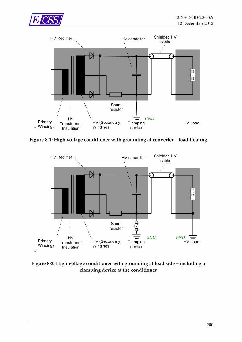
ECSS‐E‐HB‐20‐05A
12 December 2012
200
``
Figure 8‐1: High voltage conditioner with grounding at converter – load floating
``
Figure 8‐2: High voltage conditioner with grounding at load side – including a
clamping device at the conditioner
Primary Windings
HV (Secondary)Windings
HV Transformer
Insulation Clamping
device
HV Rectifier Shielded HV cable
GND
Shunt resistor
HV capacitor
HV Load
GND Primary Windings
HV (Secondary)Windings
HV Transformer
Insulation Clamping
device
HV Rectifier Shielded HV cable
GND
Shunt resistor
HV capacitor
HV Load

ECSS‐E‐HB‐20‐05A
12 December 2012
201
Figure 8‐3: High voltage conditioner with grounding at load side – including a
clamping device at the conditioner and triax HV cable for load connection
The above described measures allow to limit disturbance caused by normal operation of the high
voltage as well as avoidance of and failure propagation in case of abnormal operation, for example
with occurrence of flashover.
Intended operation during critical pressure can be typically controlled only by encapsulation, in a few
cases by control of distances (limit free gap lengths). Also here the above described measure limit
disturbances in case of unintended low pressure operation.
8.1.2 Electric propulsion
8.1.2.1 Criticality of load characterization
The EP thrusters and the power conditioner for thruster operations are typically developed separately.
In most cases, the thruster designers use standard laboratory supplies for testing, especially in early
development phases. Often, these laboratory power supplies are oversized in terms of power; they use
large filters and they are not tailored to the application. In contrary, the power conditioner developer
is recommended to follow an efficient approach, optimizing mass and efficiency and considering
long‐term degradation caused by ageing and radiation. Furthermore, the power supply designers
need to demonstrate the margins in terms of thermal and long‐term drift, including stability of the
control loop. Especially, highly optimized resonant topologies can be sensitive to load variations.
Therefore, there is an essential need for sufficient characterization of the EP load with the following
objectives:
Minimize verification of thruster supplies testing with real thruster due to high costs (test
facility)
Obtain correct load model to perform conclusive stability analysis
Establishing thruster loads models for integration into the simulation models of the power
supply
GND Primary Windings
HV (Secondary)Windings
HV Transformer
Insulation Clamping
device
HV Rectifier Shielded HV cable
GND
Shunt resistor
HV capacitor
HV Load
ECSS‐E‐HB‐20‐05A
12 December 2012
202
Control loops can be optimized during development
Allow analysis based on electrical terms and methods but not on plasma‐physical effects
The wish‐list of the power supplier for load parameters to be specified is long; however, in practice it
can be difficult to provide everything in advance to a coupling test.
Basic parameters to be specified are of course:
Max./min. operating voltage
Overvoltage, undervoltage
Max. voltage ripple
Max. output current
Overload/short/circuit conditions and behaviour
Voltage accuracy
Current accuracy (in current control mode)
As the above parameters are easy to be specified by the thruster developer, the next group of load
parameters is more difficult to determine:
Static I/V curve (current vs. voltage)
Impedance vs. frequency curve
In some cases, it can also be useful to define:
Load capacitance
Load inductance
Difficulties to provide these data can be reasoned by
Limitations to operate the thruster with a large variation of voltages and currents
Unavailability of access point or lack of test equipment to inject and measure frequency
dependent load impedances.
The situation can be even more complex due to the fact, that
Thruster can be affected by sporadic arcing and discharges
Multiple power supplies are coupled through the thruster
Plasma effects inside the thruster can cause oscillations.
Plasma effects outside of the spacecraft can interfere with the thruster and can cause oscillation
type of interference.
Therefore it depends strongly on the thruster type and on the maturity of the thruster design, which
thruster interface data can be provided to specify the powers supply correctly.
ECSS‐E‐HB‐20‐05A
12 December 2012
203
8.1.2.2 Electromagnetic compatibility of EP
The situation of EMC (Electromagnetic Compatibility) should be illuminated regarding the different
“classical” aspects
CS – Conducted susceptibility
RS – Radiated Susceptibility
CE – Conducted Emission
RE – Radiated Emission
RFC – Radiated Autocompatiblity
For CS the nominal spacecraft operating case is uncritical for high power thruster as the PPU usually
has a power converter and a filter which can be designed properly to cope with the S/C power bus
emissions. However, a special situation should be considered for transients. Those can be caused by
different effects: typical are fuse blowing transients (voltage to zero for few ms) or TDMA modes on
telecom satellites (3‐8 V repetitive transients of few ms duration). These transients can be challenging
for the design of high power conditioning in the range of some kW. To accommodate such transients
there a different strategies:
Sizing the PPU filter and regulation appropriately can result in significant mass penalties.
Switching‐off in case of fuse blowing transients can be acceptable, but interrupts thrusting.
Transferring the transient to the thruster without filtering requires an agreement with the
thruster concept, as voltage, current and thrust can run out of nominal range, but can be
acceptable if thruster is not damaged and no specific fine thrust regulation is needed.
RS is typically not an issue for EP.
With respect to conducted emissions (CE) the following aspects can be relevant:
The plasma oscillations of many thrusters are causing high frequency currents at least on the
power line between PPU and thruster. As often these power lines are floating, potential impacts
are differential mode emissions as well as common mode emissions. The differential mode
emissions can be controlled by filtering and the use of twisted shielded pairs for the supply
lines. The common mode emissions are more difficult to control as the return path can involve
the structure. In some cases this emission can be reduced by placing a proper snubber circuit
between floating power return line and structure.
Transients as a result of thruster switch‐off can be caused by contaminations in grid and on
insulator surfaces. Often such effects are difficult to predict and for some EP technologies these
spurious effects are part of the nominal operation. In most cases the spurious effects are
representing a kind of short circuit. So the PPU has to react either with a complete switch‐off or
with a current limitation mode. For high power thrusters the sudden switch‐off can cause a
problem when the EP is the main load of the spacecraft power bus. Attention should be paid,
that the bus voltage is not stepping up uncontrolled with the EP switch‐off. The current
limitation mode can result in an extra load step pulling the bus voltage down. Attention should
be given that the current rise does not trigger the protections of the spacecraft bus.
Transients as a result of non‐nominal flashovers are a risk to be considered for many thruster
principles where a surface flashover across insulators in vacuum environment cannot be
avoided by design. Impact on the spacecraft can be reduced, if a robust grounding concept is
implemented and the high voltage secondary power is sufficiently isolated from the primary
input power of the PPU.
ECSS‐E‐HB‐20‐05A
12 December 2012
204
RE can be an artefact of plasma oscillations being present in steady state as well as of transient plasma
effects (flashovers, beam‐outs), all of these effects depending on the thruster type. As these types of
emission appear in conjunction with conducted current, a proper shielding of the harness between
thruster and PPU is useful including double shielding (triax cables or equivalents).
Regarding RFC the impact of plasma on RF transmission should be addressed for the satellite
architecture).
Another effect to be considered is the magnetic emission, see impact is discussed 8.1.2.3.
8.1.2.3 Satellite Architecture Aspects
Despite the fact that of course EP is different from chemical/cold gas propulsion with impact on the s/c
architecture; there are some very specific points to make system architects aware:
Magnetic fields
Floating EP Ground
Contaminations
RF Shielding
Command and control
Flow control and valves
High Power Concepts
High Voltage Harness Specification
Some EP thrusters are using magnetic fields for controlling the plasma or to accelerate the ions. These
magnetic fields can substantially interfere with the attitude control system of the satellite, especially in
the low earth orbit, where interactions with the earth’s magnet field are likely. The situation becomes
more complex, when the magnet field is not static (i.e. produced by a permanent magnet) but is
variable depending on thruster modes. As shielding cannot provide a very efficient solution,
compensation can only be achieved by optimizing the orientation of the magnetic fields and by
considering this effect in the attitude control budgets.
The floating ground of some electrical thrusters is necessary to achieve positive or negative biasing of
the emitted plasma. As the floating voltage can reach some hundred volts, sufficient isolation should
be ensured for all floating parts including harnesses as well as proximity to MLI thermal shields.
Further, is should be highlighted, that the emitted plasma (ion beam) represents high energy
(accelerated) particles. The impinchment of the beam on satellite surfaces can cause significant erosion
on a long‐term scale. Critical is the erosion on solar arrays. For these not only the cover glasses are
very sensitive, but the inter‐cell connections as well as optical surfaces (mirrors, lenses). The emission
direction is often not limited to a narrow field of view as the plasma plume often has a wide angel.
Another effect to consider is the shielding effect of the plasma beam, which can be less transparent for
radio frequencies and therefore can impact the performance of RF transmissions.
In view of both phenomena, the plasma erosion as well as the RF shielding, a good characterization of
the plasma beam is necessary to be aware of the plume angel, energy distribution and shielding
characteristics. Based on this information, the location of thrusters on the satellite can be better
defined, avoiding critical configurations.
Regarding the command and control architecture a lot of additional functions are required to operate
the thruster, including power supplies for neutralizer, heaters and valves. This subsystem needs an
internal control to manage all the functions and to allow control by the spacecraft. Depending on the
ECSS‐E‐HB‐20‐05A
12 December 2012
205
complexity of the control tasks, the electric propulsion subsystem requires either hardwired control
logic or a powerful microcontroller. The more autonomy is given to the subsystem, the higher the
effort to spend – in terms of complexity and cost. In case that control algorithms are transferred into
the responsibility of the satellites onboard computer (rather than in the PPU) it is necessary to foresee
an adequate AIT strategy as a closed loop test of EP and satellite, is difficult to arrange (see section
8.1.2.4).
In view of control it is worth to mention, that the EP concepts based on ionized gases require
regulation valves to control the gas flow at very low rates. Their characteristic is very non‐linear and
imposes some complexities in the regulation algorithms.
In case, those high power thrusters of several kW are embarked on satellites, the satellites power
system architecture could be revised in specific cases. For example: it may not be useful to combine a
regulated spacecraft bus with a power conditioner using an individual wide range regulator as well.
For some electrical thrusters the question should be asked, to which extend a regulation is necessary,
or if for certain spacecraft modes a wider drift of voltage and currents is acceptable for the EP system.
Also the fusing concept can be adapted, especially if electronic fuses, LCL’s (latching current limiters)
are used. For high power thrusters it can be difficult to tailor the protecting latching current limiters of
the satellites power system. Instead, the protection function can be transferred to the power
conditioner, which is dedicated to control higher power and current.
The high voltage harness typically connects the PPU, which is located inside the spacecraft, to the
thruster(s) which is/are located outside of the spacecraft. A proper specification is needed to cover the
specific aspects of high voltage (levels, ratings), possible high temperatures in vicinity of the thruster
(everything above 120 °C can be critical), need of insulated connection terminals (as suitable high
voltage connectors typically are not available), high radiation environment outside of the spacecraft,
bending flexibility (if thruster pointing mechanisms are used), need of shielding and floating ground
operation (can need triax shielding), and safety aspects.
8.1.2.4 Assembly, Integration and Test Issues of EP
The AIT (Assembly, Integration and Test) of EP systems on satellites is affected by the fact, that end‐
to‐end testing of the propulsion subsystem is limited and by the specifics of high voltage and high
power use.
As it is not possible to run the thruster together with the spacecraft in a vacuum facility, testing of the
subsystem should be “sliced”. On subsystem level, the thruster is typically first characterized with the
aid of lab power supplies and later tested coupled with the PPU. On satellite level the thruster cannot
be operated, thus the PPU should be integrated onto the satellite using a thruster simulator
respectively a load simulator. The thruster simulation should be done with a representative load
simulator. It should be highlighted, that the load simulator can be a challenging development as it has
to handle high voltage and high power (for some EP systems several kW). To be representative
regarding EMC aspects the load simulation should be highly dynamic and possibly include transient
and high frequency ripple simulation (plasma oscillation).
In view of EMC testing on subsystem and on unit level it should be highlighted, that the Line
Impedance Simulation Network (LISN) is typically not suitably defined for high power loads as like
large EP systems. The definition of this item should be tailored in a suitable way.
As a last point it should be pointed out, that the high voltage harness used for most of the EP systems
introduces some complexity for satellite AIT, as suitable high voltage connectors are not available for
space application (only for some ground testing). A typical workaround is the use of splice blocks and
terminals to perform cable interconnections. Consequently, such solutions are not “plug‐and‐play”,
because they require specific procedures and checks, and not to forget: some safety hazards due to
accessible open high voltage.
ECSS‐E‐HB‐20‐05A
12 December 2012
206
Last but not least and worth to mention: the high power thrusters for EP suffer from high
temperatures at the thruster interfaces. Often for the selection of a suitable high voltage cable, the
difficulty occurs that qualified HV cables for operation beyond 180 °C are often not available.
8.1.3 Electron devices (tubes) Electron devices like travelling wave tubes or klystron are equipment with highly optimised high
voltage insulations. As in space projects they are typically used as qualified equipment according to
their dedicated design rules here only the effects affecting the interface to the high voltage power
conditioners are highlighted.
Most relevant for the interface is the effect of “spurious”, which means that it cannot be excluded, that
breakdowns or pre‐breakdowns occur in the high voltage vacuum insulation of the tube. Although the
events are typically rare, the power conditioner should be hardened against this by:
Implementation of current limiting element (for example: resistors)
Consideration of changed voltage and field distribution in the insulation as a consequence the
“spurious”
Measures to maintain EMC
Furthermore, electron devices are typically manufactured with flying leads for the high voltage
interface. As high voltage connectors are not available and are avoided, the flying leads are connected
to the power conditioner either via “open” terminal blocks (in the minority of applications) or are
“potted” with the HV insulation of the electronic power conditioner (the typical case). Potting on both
ends gives some limitation on reparability, integration and testability (after potting).
8.1.4 Scientific instruments and experiments In the frame of scientific instruments and experiments the following case of high voltage application
can require special attention:
AC high voltage sources
AC high voltage sources are sometimes requested with modulated frequency and amplitude. The
main problem is that the high AC voltage can cause significant degradation of the high voltage
insulation by partial discharges. The insulations should be specially designed for this kind of stress.
High voltage cables (and HV insulation in general) typically requires a gap free interface between
conductor and insulation. High voltage transformers are single staged and need careful control of the
electrical fields by proper shaping and shielding.
8.1.5 EMC aspects Related to high voltage the following EMC effects need to be taken into consideration and to be
assessed:
High electrical field strengths in the environment of the high voltage circuit
High magnetic field strengths in presence of high currents (transients, breakdown)
High electromagnetic field strengths in presence of high currents (transients, breakdown)
High currents on return lines (structure)
High ripple on high voltage lines
Propagation of high voltage into low voltage circuitry in case of failure
ECSS‐E‐HB‐20‐05A
12 December 2012
207
As a consequence the following general recommendations are given:
a. High voltage and low voltage electronic circuits should be separated sufficiently by means of
galvanic isolation
spacing
electrostatic shield
overvoltage suppression at critical inputs of sensitive low voltage circuits
for more details see section 8.1.1.
b. Discharge currents and energies should be limited (resistors or actively).
c. High voltage supply lines and their return lines should be routed close together in case of risk
of high currents
d. Shielded high voltage lines should be used (as far as possible) when power harness is routed
outside of the high voltage equipments.
e. High voltage units should be shielded in general (as far as possible) by metallic or metallized
structures with proper grounding.
f. Floating high voltage grounds should be avoided – and if floating, limit the floating range by
clamping devices.
ECSS‐E‐HB‐20‐05A
12 December 2012
208
9 Hazards and safety
9.1 Hazards The typical hazards related to high voltage and its applications are:
Electrical Shock
In some cases:
Acoustic noise
X‐Ray Radiation
Explosions
The electrical shock is applicable if certain levels of voltage or current or energy are exceeded (see
section 9.2).
Acoustic noise or explosion are possible typically in case of high voltage breakdown, sparks and arcing,
either due to destruction of high voltage insulations or by ignition of explosive substances (if present).
X‐Ray radiation can be generated if high voltage is applied in a high vacuum and a sufficiently high
current is flowing through the vacuum insulation caused by arcing, plasma or surface discharge. The
effect depends on the voltage, on the current and the interacting surface material.
9.2 Safety Safety can be ensured by respecting the applicable safety standards and performance of adequate risk
assessments with implementation of measures for risk reduction.
It is proposed to address all high voltage related risks in a risk management plan and in critical
items list.
As a specific standard for testing with high voltage it is proposed to respect
European Standard: “Erection and Operation of Electrical Test Equipment” (EN 50191:2000)
With respect to the standard it is worth to mention, that the standard is applicable to the erection and
operation of fixed and temporary electrical test installations under the following conditions:
Voltages at frequencies below 500 Hz are higher than 25 V AC or 60 V DC.
The resulting current through a 2 kΩ resistor exceeds 3 mA(r.m.s.) AC or 12 mA DC.
The resulting current for voltages at frequencies above 500 Hz exceeds the values defined in the
EN.
Or
The discharge energy exceeds 350 mJ.
In case of ambiguities between the EN standard and this text, the standard is always applicable.
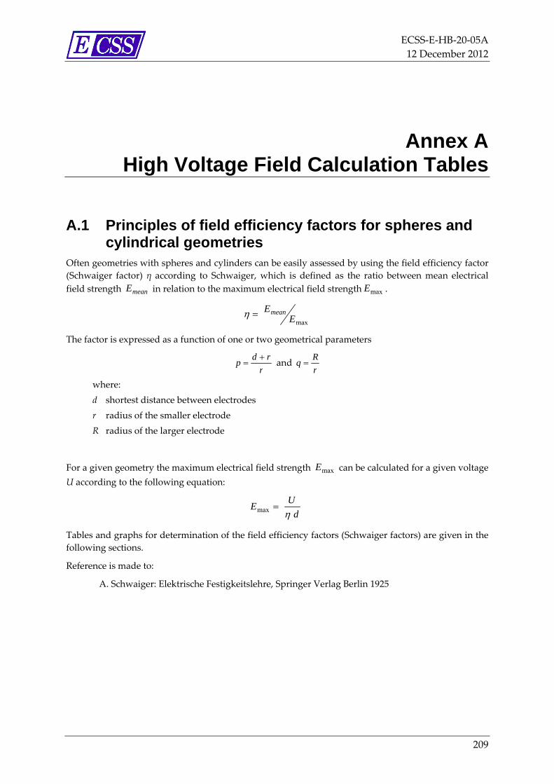
ECSS‐E‐HB‐20‐05A
12 December 2012
209
Annex A High Voltage Field Calculation Tables
A.1 Principles of field efficiency factors for spheres and cylindrical geometries
Often geometries with spheres and cylinders can be easily assessed by using the field efficiency factor
(Schwaiger factor) η according to Schwaiger, which is defined as the ratio between mean electrical
field strength meanE in relation to the maximum electrical field strength maxE .
maxEEmean
The factor is expressed as a function of one or two geometrical parameters
r
rdp
and
r
Rq
where:
d shortest distance between electrodes
r radius of the smaller electrode
R radius of the larger electrode
For a given geometry the maximum electrical field strength maxE can be calculated for a given voltage
U according to the following equation:
d
UE
max
Tables and graphs for determination of the field efficiency factors (Schwaiger factors) are given in the
following sections.
Reference is made to:
A. Schwaiger: Elektrische Festigkeitslehre, Springer Verlag Berlin 1925
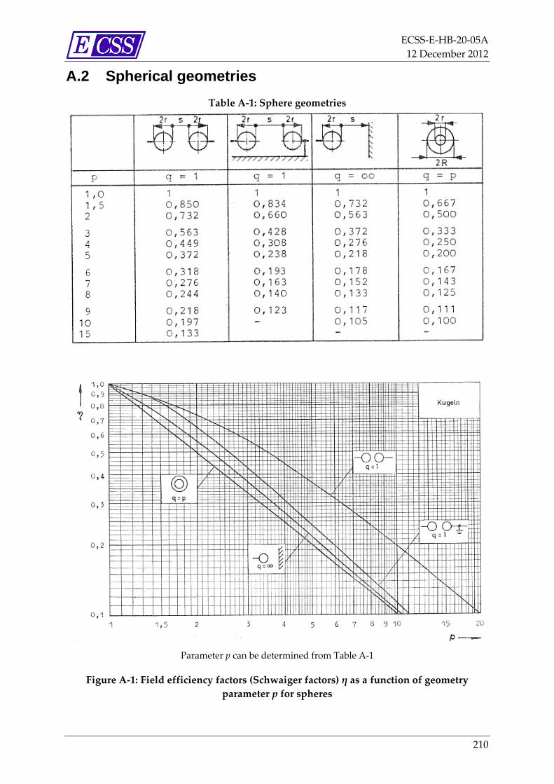
ECSS‐E‐HB‐20‐05A
12 December 2012
210
A.2 Spherical geometries
Table A‐1: Sphere geometries
Parameter p can be determined from Table A‐1
Figure A‐1: Field efficiency factors (Schwaiger factors) η as a function of geometry
parameter p for spheres
ECSS‐E‐HB‐20‐05A
12 December 2012
211
A.3 Cylindrical geometries
Table A‐2: Cylinder‐parallel‐to‐a‐cylinder geometries
Table A‐3: Cylinder‐inside‐a‐cylinder geometries
ECSS‐E‐HB‐20‐05A
12 December 2012
212
Parameter p can be determined from Table A‐2
Figure A‐2: Field efficiency factors (Schwaiger factors) η as a function of geometry
parameter p for cylinders
Parameter p can be determined from Table A‐3.
Figure A‐3: Field efficiency factors (Schwaiger factors) η as a function of geometry
parameter p for cylinders
ECSS‐E‐HB‐20‐05A
12 December 2012
213
Annex B Best Practice References
B.1 High Voltage Evaluation Plan
B.1.1 Evaluation Activities
For new equipments, modules and components/parts used in flight hardware, an evaluation should
be established and the agreed/proposed tasks should be performed to ensure and safeguard a proper
qualification of the subjected item.
B.1.2 Evaluation Plan
An Evaluation Plan should be produced planning the thorough investigation and characterisation of
the technologies and materials proposed for integration in HV equipment. For each technology a
categorisation should be used to determine, based on existing heritage if any, the work that should be
performed. This categorisation should follow the guidelines of Table B‐1. A short Requirement
Specification should also be established as a guide for the Evaluation objectives.
Evaluation should be performed on individual parts, materials and processes including subassemblies
and modules.
The Evaluation Plan should include where appropriate:
The characterisation of ageing behaviour,
The temperature behaviour in conjunction with neighbouring technologies and materials,
The performance in partial pressure,
The influence of electrical parameters such as voltage, field, power, AC and DC.
Every effort should be made to ensure that the technologies and materials are flight compatible and
relevant in terms of, for example, outgassing and properties over flight temperature range, radiation
environment, availability, practical implementation, quality control of process and supplier, prior to
beginning the evaluation.
The Evaluation plan should be agreed with the procuring entity.
A Test plan should be produced for each evaluation planned. The number of samples evaluated
should be sufficient to allow parallel tests, including where appropriate “control” samples, with a
view to reducing the cost and time associated with the test facilities; and to ensure that the results are
reliable. A minimum of 3 samples, and preferably 5, should be used to “majority vote” important
results.
ECSS‐E‐HB‐20‐05A
12 December 2012
214
The output of this segment should be:
An agreed Evaluation plan.
An agreed Requirement Specification for each Technology
An agreed Test Plan for each Technology
B.1.3 Manufacturing of Evaluation Samples
The required relevant number of samples of the various technologies and materials that should be
tested should be manufactured. At the end of manufacturing, an Evaluation TRR should be held on
the basis of Test Procedures generated from the Test Plans.
The output of this segment should be:
An agreed Test Procedure for each Technology
Manufactured Evaluation Samples
Successful Evaluation TRR.
B.1.4 Test and Characterisation
Following the manufacturing of Evaluation samples these samples should be tested according to Test
Procedures agreed in the Evaluation TRR.
The output of this segment should be
Raw Test Results
B.1.5 Evaluation Review
The work performed in this Task should be submitted to the Agency for approval in a dedicated
Evaluation Review.
The Review data package should include an Evaluation Report, in which the test results are
summarised. They should be reviewed for their compliance to the requirement specifications. Results
should be discussed with respect to the agreed objectives of the Evaluation Plan, and analysed with
respect to available ‘state of the art’ scientific knowledge.
Wherever possible, all statements made in the report, including predicted trends and assumptions,
should be justified with detailed discussions at a technical level.
The output of this segment should be:
The Evaluation Review data pack
A successful Evaluation Review
Agreed technologies and materials to be qualified.

ECSS‐E‐HB‐20‐05A
12 December 2012
215
Table B‐1: Product categories according to heritage (Ref.: ECSS‐E‐ST‐10‐02C)
Category Description Qualification programme
A Off‐the‐shelf product without modifications and
• subjected to a qualification test programme at
least as severe as that imposed by the actual
project specifications including environment
• produced by the same manufacturer or
supplier and using the same tools and
manufacturing processes and procedures
None
B Off‐the‐shelf product without modifications.
However:
It has been subjected to a qualification test
programme less severe or different to that
imposed by the actual project specifications
(including environment).
Delta qualification
programme, decided on a
case by case basis.
C Off‐the‐shelf product with modifications.
Modification includes changes to design, parts,
materials, tools, processes, procedures, supplier,
or manufacturer.
Delta or full qualification
programme (including
testing), decided on a case by
case basis depending on the
impact of the modification.
D Newly designed and developed product. Full qualification programme.
B.2 Materials Evaluation A typical material evaluation should consider
Physical property tests
Electrical property tests
Technology sample tests
A typical flow is shown in Figure B‐1.
Physical and electrical properties should be determined to standard methods applicable for the type of
material. For determination of electrical parameters like electrical breakdown strengths a suitable
sample design needs to be selected. Some options are:
Rogowky profile electrodes (to be embedded in potting materials) – see Figure B‐2
Close‐to‐application electrodes, for example crossed wire electrodes ‐ see Figure B‐3
Material disk between shaped electrodes ‐ see Figure B‐4
The electrode separation is 1 mm.
A statistical relevant number of samples should be selected. For breakdown tests 10 samples per test
parameter should be used as a minimum.
After determination of physical and electrical properties the material selection should be confirmed
and further evaluated by “technology samples”.
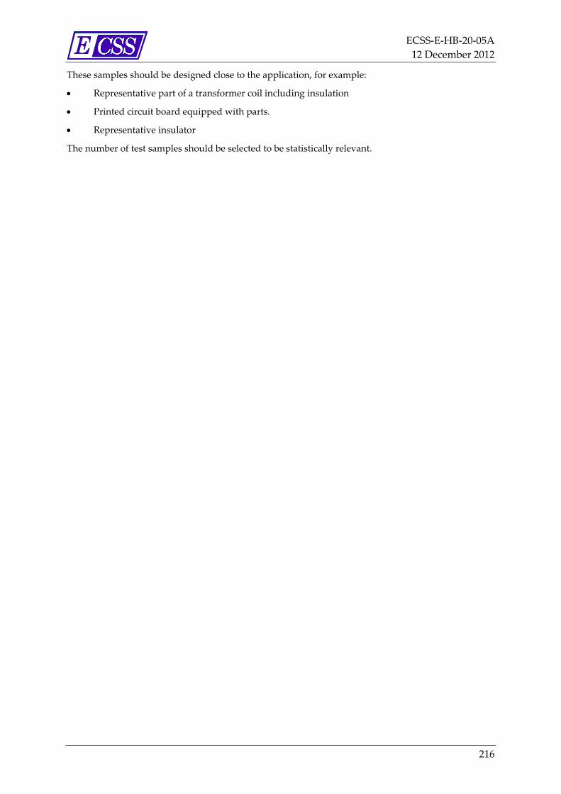
ECSS‐E‐HB‐20‐05A
12 December 2012
216
These samples should be designed close to the application, for example:
Representative part of a transformer coil including insulation
Printed circuit board equipped with parts.
Representative insulator
The number of test samples should be selected to be statistically relevant.
ECSS‐E‐HB‐20‐05A
12 December 2012
217
Figure B‐1: Typical material evaluation flow
Physical Property Tests
E-Modulus
Coefficient of Thermal Expansion
Glass Transition Point
Shore Hardness
Thermal Conductivity
Breakdown Strength
Permeability
Dielectric Loss Factor
Electrical Property Tests
Bulk insulation resistance
Surface conductivity
Breakdown Strength
Partial Discharge Test
Technology Sample Tests
Lifetime test (Stress-Lifetime Curve)
Electrical Characterization
DPA
Selection
Result

ECSS‐E‐HB‐20‐05A
12 December 2012
218
Figure B‐2: Potted Rogowsky‐profile electrodes
Electrodes
Potting
Figure B‐3: Crossed wire electrode
Figure B‐4: Material disk between electrodes
Electrodes
Sample
ECSS‐E‐HB‐20‐05A
12 December 2012
219
B.3 PID – Process Identification Document In order to avoid redundancy with other internal company documents, a PID could consist of a list of
configured documents (manufacturing+tests, control, other if any). The PID then only points to the
relevant documents (and chapter), where the required information can be found.
The PID should consist of the following documentation:
Section 1:
Reference documents
Short description of the concerned technologies
Application area of the technologies.
Section 2:
Manufacturing flow chart taking into account all the different steps as well as all intermediate
quality control steps. All processes should be properly configured
Section 3:
Configured Items Data List including document reference number, version and issue:
Listing of the quality system,
Listing of the procurement specifications
Listing of all the manufacturing processes
Listing of the quality control processes
Section 4:
Organigram of the company
Description of the different key personnel (optional)
Section 5:
Description of the different steps used to manufacture the product. An example of the log sheet
and or travel sheet is preferred.
Section 6:
List of all materials used to manufacture the final product
Section 7:
Working area description (a map is sufficient)
Section 8:
Listing of all equipment used to manufacture the final product:
Manufacturing equipment
Control equipment.
Section 9:
Listing of all the test facilities
All deviations from the PID should be considered as being outside qualification.


![REP002, [ARCHIVED] - ESCIES](https://static.fdocuments.in/doc/165x107/616a52b711a7b741a3513e5a/rep002-archived-escies.jpg)