SP14Q006-T-8 - Kaohsiung Opto-Electronics Official · PDF file · 2012-06-17Title:...
23
FOR MESSRS: DATE: May 1 st ,2012 CUSTOMER’S ACCEPTANCE SPECIFICATIONS SP14Q006-T Contents No. ITEM SHEET No. PAGE 1 COVER 7B64PS 2701-SP14Q006-T-8 1-1/1 2 RECORD OF REVISION 7B64PS 2702-SP14Q006-T-8 2-1/2~2/2 3 GENERAL SPECIFICATION 7B64PS 2703-SP14Q006-T-8 3-1/1 4 ABSOLUTE MAXIMUM RATINGS 7B64PS 2704-SP14Q006-T-8 4-1/1 5 ELECTRICAL CHARACTERISTICS 7B64PS 2705-SP14Q006-T-8 5-1/2~2/2 6 OPTICAL CHARACTERISTICS 7B64PS 2706-SP14Q006-T-8 6-1/3~3/3 7 BLOCK DIAGRAM 7B64PS 2707-SP14Q006-T-8 7-1/1 8 INTERFACE TIMING CHART 7B64PS 2708-SP14Q006-T-8 8-1/3~3/3 9 OUTLINE DIMENSIONS 7B64PS 2709-SP14Q006-T-8 9-1/2~2/2 10 APPEARANCE STANDARD 7B64PS 2710-SP14Q006-T-8 10-1/3~3/3 11 PRECAUTION IN DESIGN 7B64PS 2711-SP14Q006-T-8 11-1/2~2/2 12 DESIGNATION OF LOT MARK 7B64PS 2712-SP14Q006-T-8 12-1/1 13 PRECAUTION FOR USE 7B64PS 2713-SP14Q006-T-8 13-1/1 ACCEPTED BY: PROPOSED BY: KAOHSIUNG OPTO-ELECTRONICS INC. SHEET NO. 7B64PS 2701-SP14Q006-T-8 PAGE 1-1/1
Transcript of SP14Q006-T-8 - Kaohsiung Opto-Electronics Official · PDF file · 2012-06-17Title:...

FOR MESSRS: DATE: May 1st ,2012
CUSTOMER’S ACCEPTANCE SPECIFICATIONS
SP14Q006-T
Contents
No. ITEM SHEET No. PAGE
1 COVER 7B64PS 2701-SP14Q006-T-8 1-1/1
2 RECORD OF REVISION 7B64PS 2702-SP14Q006-T-8 2-1/2~2/2
3 GENERAL SPECIFICATION 7B64PS 2703-SP14Q006-T-8 3-1/1
4 ABSOLUTE MAXIMUM RATINGS 7B64PS 2704-SP14Q006-T-8 4-1/1
5 ELECTRICAL CHARACTERISTICS 7B64PS 2705-SP14Q006-T-8 5-1/2~2/2
6 OPTICAL CHARACTERISTICS 7B64PS 2706-SP14Q006-T-8 6-1/3~3/3
7 BLOCK DIAGRAM 7B64PS 2707-SP14Q006-T-8 7-1/1
8 INTERFACE TIMING CHART 7B64PS 2708-SP14Q006-T-8 8-1/3~3/3
9 OUTLINE DIMENSIONS 7B64PS 2709-SP14Q006-T-8 9-1/2~2/2
10 APPEARANCE STANDARD 7B64PS 2710-SP14Q006-T-8 10-1/3~3/3
11 PRECAUTION IN DESIGN 7B64PS 2711-SP14Q006-T-8 11-1/2~2/2
12 DESIGNATION OF LOT MARK 7B64PS 2712-SP14Q006-T-8 12-1/1
13 PRECAUTION FOR USE 7B64PS 2713-SP14Q006-T-8 13-1/1
ACCEPTED BY: PROPOSED BY:
KAOHSIUNG OPTO-ELECTRONICS INC. SHEETNO. 7B64PS 2701-SP14Q006-T-8 PAGE 1-1/1

RECORD OF REVISION
DATE SHEET No. SUMMARY
Jan.16,’03 7B64PS 2705 - SP14Q006-T-2 PAGE 5 - 2/2
5.2 ELECTRICAL CHARACTERISTICS OF LED BACKLIGHT
SYMBOL TYP. MAX
VLED (TBD) -
ILED 60 -
Revised↓ SYMBOL TYP. MAX
VLED 5 5.2
ILED 160 -
Oct.22,’03 7B64PS2709- SP14Q006-T-3 Page 9-2/2
Changed LED I/F JAE/1L-G-4S-S3C2 → JAE/IL-G-4S-S3C2
Mar.24,’04 7B64PS2708- SP14Q006-T-4 Page 8-3/3
8.3 POWER ON/OFF TIMING SEQUENCE Revised tDLD min. 200 → 50 Revised tCH max. 200 → 30
Jun.04,’04 7B64PS 2705-
SP14Q006-T-5 Page 5-1/2
5.1 ELECTRICAL CHARACTERISTICS Added
ITEM SYMBOL MIN. TYP. MAX
Power Supply Voltage Logic VDD-VSS 3.2 3.3 3.4
Recommend LC Driving Voltage
VDD-V0
21.0 22.0 23.0
20.0 21.0 22.0
19.0 20.0 21.0
7B64PS 2706-
SP14Q006-T-5 Page 6-3/3
6.2 OPTICAL CHARACTERISTICS OF BACKLIGHT Added The LCD driving voltage should be adjusted at the
voltage where the peak contrast is obtained.
7B64PS 2710-
SP14Q006-T-5 Page 10-1/3
10.1 APPEARANCE INSPECTION CONDITION Revised 45°25°
May.04,’07 7B64PS 2703 – SP14Q006-T-6 Page 3-1/1
3. GENERAL SPECIFICATIONS Added (11) Backlight Type LED(Color : white)
↓
(11) Backlight Type LED(Color : white) Life time : 40Kh @ 25℃
Note : Life time for half of initial brightness
KAOHSIUNG OPTO-ELECTRONICS INC. SHEETNO. 7B64PS 2702-SP14Q006-T-8 PAGE 2-1/2

RECORD OF REVISION
DATE SHEET No. SUMMARY
May.04,’07 7B64PS 2705 – SP14Q006-T-6 Page 5-2/2
5.2 ELECTRICAL CHARACTERISTICS OF LED BACKLIGHT Revised
7B64PS 2712 – SP14Q006-T-6 Page 12-1/1
12. DESIGNATION OF LOT MARK Added REVISION A
Mar.06,’09
7B64PS 2712 SP14Q006-T-7
PAGE 12-1/1
12. DESIGNATION OF LOT MARK Revised reversion from REV. A to REV.B
May.01,’12 All pages Company name changed: KAOHSIUNG HITACHI ELECTRONICS CO.,LTD.
KAOHSIUNG OPTO-ELECTRONICS INC.
→
Ambient Temperature(℃) allo
wab
le
forw
ard
cu
rren
t
(mA
/pcs
)
KAOHSIUNG OPTO-ELECTRONICS INC. SHEETNO. 7B64PS 2702-SP14Q006-T-8 PAGE 2-2/2
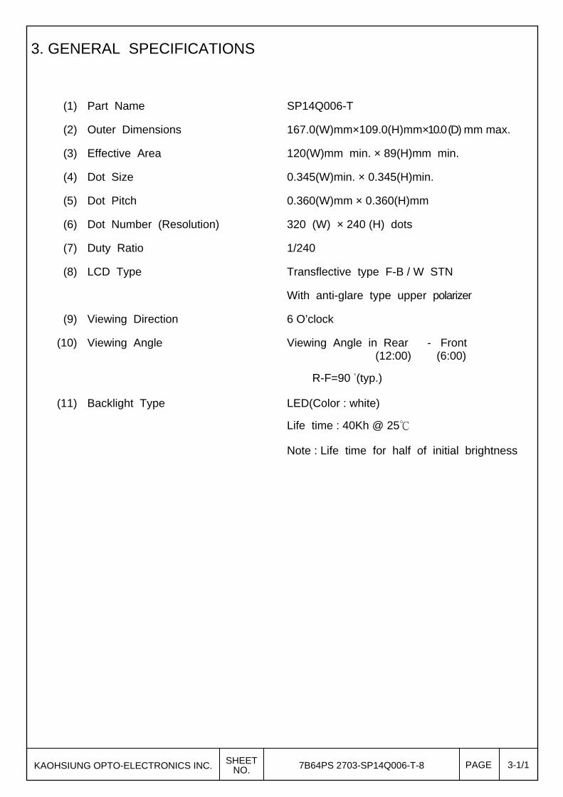
3. GENERAL SPECIFICATIONS
(1) Part Name SP14Q006-T
(2) Outer Dimensions 167.0(W)mm×109.0(H)mm×10.0 (D) mm max.
(3) Effective Area 120(W)mm min. × 89(H)mm min.
(4) Dot Size 0.345(W)min. × 0.345(H)min.
(5) Dot Pitch 0.360(W)mm × 0.360(H)mm
(6) Dot Number (Resolution) 320 (W) × 240 (H) dots
(7) Duty Ratio 1/240
(8) LCD Type Transflective type F-B / W STN
With anti-glare type upper polarizer
(9) Viewing Direction 6 O’clock
(10) Viewing Angle Viewing Angle in Rear - Front (12:00) (6:00)
R-F=90 °(typ.)
(11) Backlight Type LED(Color : white)
Life time : 40Kh @ 25℃
Note : Life time for half of initial brightness
KAOHSIUNG OPTO-ELECTRONICS INC. SHEETNO. 7B64PS 2703-SP14Q006-T-8 PAGE 3-1/1
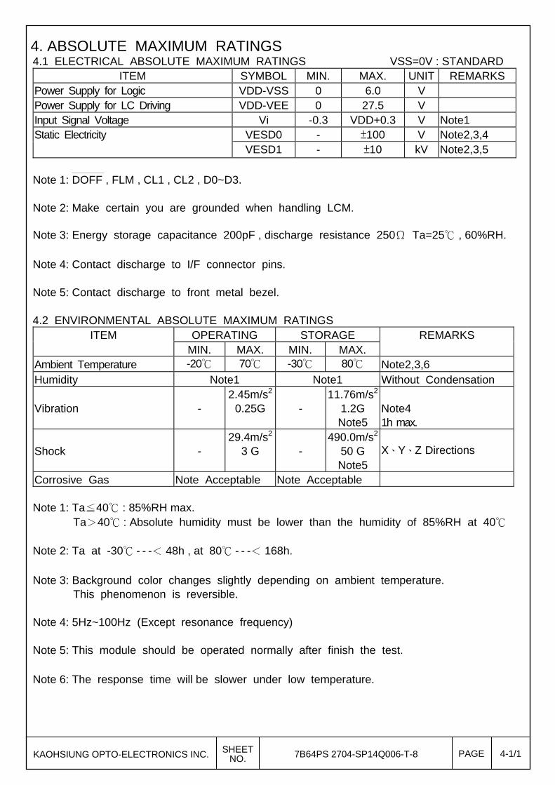
4. ABSOLUTE MAXIMUM RATINGS 4.1 ELECTRICAL ABSOLUTE MAXIMUM RATINGS VSS=0V : STANDARD
ITEM SYMBOL MIN. MAX. UNIT REMARKS Power Supply for Logic VDD-VSS 0 6.0 V Power Supply for LC Driving VDD-VEE 0 27.5 V Input Signal Voltage Vi -0.3 VDD+0.3 V Note1 Static Electricity VESD0 - ±100 V Note2,3,4
VESD1 - ±10 kV Note2,3,5
Note 1: DOFF , FLM , CL1 , CL2 , D0~D3. Note 2: Make certain you are grounded when handling LCM. Note 3: Energy storage capacitance 200pF , discharge resistance 250Ω Ta=25℃ , 60%RH. Note 4: Contact discharge to I/F connector pins. Note 5: Contact discharge to front metal bezel. 4.2 ENVIRONMENTAL ABSOLUTE MAXIMUM RATINGS
ITEM OPERATING STORAGE REMARKS MIN. MAX. MIN. MAX. Ambient Temperature -20℃ 70℃ -30℃ 80℃ Note2,3,6 Humidity Note1 Note1 Without Condensation Vibration
-
2.45m/s2
0.25G -
11.76m/s2
1.2G Note5
Note4 1h max.
Shock
-
29.4m/s2
3 G -
490.0m/s2
50 G Note5
X、Y、Z Directions
Corrosive Gas Note Acceptable Note Acceptable Note 1: Ta≦40℃ : 85%RH max. Ta>40℃ : Absolute humidity must be lower than the humidity of 85%RH at 40℃ Note 2: Ta at -30℃ - - -< 48h , at 80℃ - - -< 168h. Note 3: Background color changes slightly depending on ambient temperature. This phenomenon is reversible. Note 4: 5Hz~100Hz (Except resonance frequency) Note 5: This module should be operated normally after finish the test. Note 6: The response time will be slower under low temperature.
KAOHSIUNG OPTO-ELECTRONICS INC. SHEETNO. 7B64PS 2704-SP14Q006-T-8 PAGE 4-1/1

5. ELECTRICAL CHARACTERISTICS 5.1 ELECTRICAL CHARACTERISTICS
I T E M SYMBOL CONDITION MIN. TYP. MAX. UNIT REMARKS
Power Supply Voltage for Logic
VDD-VSS - 4.75 5.0 5.25
V 3.2 3.3 3.4
Power Supply Voltage for LC Driving
VEE-VSS - -23.1 -22.0 -20.9 V
Input Signal Voltage Vi H LEVEL 0.8VDD - VDD V
Note1 L LEVEL 0 - 0.2VDD V
Power Supply Current for Logic
IDD VDD-VSS=5.0V
VEE-VSS= -22.0V- 6.0 - mA Note2
Power Supply Current for LC Driving
IEE VDD-VSS=5.0V
VEE-VSS= -22.0V - 5.0 - mA Note2
Recommended LC Driving Voltage
VDD-V0
Ta= 0℃ , = 0∘ 21.0 22.0 23.0 V
Note3 Ta=25℃ , = 0∘ 20.0 21.0 22.0 V
Ta=50℃ , = 0∘ 19.0 20.0 21.0 V
Frame Frequency fFLM - 70 75 80 Hz Note4
Note 1: DOFF , FLM , CL1 , CL2 , D0~D3. Note 2: FLM=75Hz , test pattern is all “Q”. VDD-V0=21.0V , Ta=25℃ Note 3: Recommended LC driving voltage may fluctuate about ±1.0V by each module. Test pattern is all “Q”
Note 4: Please set the frame frequency so as to avoid flicker and rippling on the display.
KAOHSIUNG OPTO-ELECTRONICS INC. SHEETNO. 7B64PS 2705-SP14Q006-T-8 PAGE 5-1/2

5.2 ELECTRICAL CHARACTERISTICS OF LED BACKLIGHT
ITEM SYMBOL CONDITION MIN. TYP. MAX. UNIT REMARKS
Power Supply Voltage for LED
VLED - - 5.0 5.2 V
Power Supply Current for LED
ILED VLED=5.0V - 160 - mA Note1
Note 1: The ILED changes depending on ambient temperature.
Ambient Temperature(℃) allo
wab
le f
orw
ard
cur
rent
(mA
/pcs
)
KAOHSIUNG OPTO-ELECTRONICS INC. SHEETNO. 7B64PS 2705-SP14Q006-T-8 PAGE 5-2/2

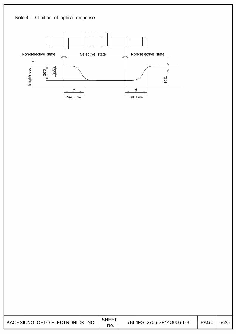

6.2 OPTICAL CHARACTERISTICS OF BACKLIGHT (Backlight ON)
I T E M MIN. TYP. MAX. UNIT REMARKS
Brightness - 60 - cd/m2 ILED=160mA
Brightness Uniformity - - ±30 % Note1
Ta=25℃, Display data should be all “ON”.
The LCD driving voltage should be adjusted at the voltage where the peak contrast is obtained.
Note 1: Measure of the following 9 places on the display.
Definition of the brightness tolerance.
Y=240Y=160Y=80
X=60
X=120
X=180
Average Brightness
Max. or Min. Brightness-Average Brightness x 100% ( )
KAOHSIUNG OPTO-ELECTRONICS INC. SHEETNO. 7B64PS 2706-SP14Q006-T-8 PAGE 6-3/3

D0~
D3
FLM
CL1
DO
FF
CL2
IC4
320×
240
DO
TS
IC2
: T
IMIN
G C
IRC
UIT
D0
D
1
D2
IC1
X24
0
D3
X1
X81
X16
1
X16
0
X24
0
X80
X1
IC5
IC6
IC7
PO
WE
R
SU
PP
LY
LE
D
Bac
k L
igh
t
VD
D
VS
S
V0
VE
E
VLE
D(-
)
VLE
D(+
)
Y320
Y241
Y160
Y81
Y80
Y1
7. BLOCK DIAGRAM
KAOHSIUNG OPTO-ELECTRONICS INC. SHEETNO. 7B64PS 2707-SP14Q006-T-8 PAGE 7-1/1

8. INTERFACE TIMING CHART 8.1 INTERFACE TIMING CHART
52.1s≦T≦59.5s
X1 X2 X240
CL1
CL2
D3
D2
D1
D0
FLM
CL1
FLM
D0~D3 X1 X2 X239 X240
240×T
Y1 Y5 Y317
Y2 Y6 Y318
Y3 Y7 Y319
Y4 Y8 Y320
KAOHSIUNG OPTO-ELECTRONICS INC. SHEETNO. 7B64PS 2708-SP14Q006-T-8 PAGE 8-1/3

8.2 TIMING CHARACTERISTICS
ITEM SYMBOL MIN. TYP. MAX. UNITCL2 frequency fCP - - 6.5 MHzCL2 pulse width tw 45 - - ns CL2 rise, fall time tr,tf - - 15 ns Data set up time tDSU 30 - - ns Data hold time tDHD 30 - - ns CL1 set up time tLSU 80 - - ns CL1 clock time tLC 120 - - ns “FLM” set up time tSETUP 100 - - ns “FLM” hold time tHOLD 100 - - ns “CL1” pulse width twc 125 - - ns
tw twtw
CL2
tDSU tDHD
D0~D3
tLC tLSU
CL1
twc
tSETUP tHOLD
FLM
0.2VDD
0.8VDD
tf tr
0.2VDD
0.8VDD
0.2VDD
0.8VDD
0.2VDD
0.8VDD
0.2VDD
0.8VDD
0.2VDD
0.8VDD
0.2VDD
0.8VDD
0.2VDD
0.8VDD
0.2VDD
0.8VDD
0.2VDD
0.8VDD
0.8VDD 0.8VDD
KAOHSIUNG OPTO-ELECTRONICS INC. SHEETNO. 7B64PS 2708-SP14Q006-T-8 PAGE 8-2/3

8.3 POWER ON/OFF TIMING SEQUENCE
SYMBOL MIN. MAX. UNIT REMARKS
tDLD 50 - ms tCH 0 30 ms Note1
tLDH 0 - ms tDOr - 100 ns tDOf - 100 ns
tDLCr 0 - ms Note2 tDLCf 0 - ms tDLCs 20 - ms
Note 1: Please keep the specified sequence because wrong sequence may cause permanent damage to the LCD panel. Note 2: KOE recommends you to use DOFF function. Display quality may deteriorate if you don‘t use DOFF function. 8.4 POWER SUPPLY FOR LCM (EXAMPLE)
Note 1 : VR : 10k
tDLD tDLD
tCH tCH
tDLCr tDLCf
tDLCstDLCs
tLDH
tDOr tDOf
tLDH
0.8VDD 0.8VDD
0.8VDD 0.8VDD
0.2VDD0.2VDD
VDD
SIGNAL
DOFF
GND
GND
VEE GND
GND
0.95VDD0.95VDD
LCM
VDD
VSS
VEE
VRV0
+5.0V
-22.0V
KAOHSIUNG OPTO-ELECTRONICS INC. SHEETNO. 7B64PS 2708-SP14Q006-T-8 PAGE 8-3/3


9.2 DISPLAY PATTERN 9.3 INTERFACE PIN CONNECTION FPC:pitch 1.25mm 14 pins
INTERFACE PIN No. SIGNAL LEVEL FUNCTION LCM CN1 1 D0 H/L Display Data
2 D1 3 D2 4 D3 5 DOFF H/L H : ON / L : OFF 6 FLM H First Line Marker 7 N.C - - 8 CL1 HL Data Latch
9 CL2 HL Data Shift 10 VDD - Power Supply for Logic 11 VSS - GND 12 VEE - Power Supply for LC 13 V0 - Operating Voltage LC Driving 14 VSS - GND
INTERFACE PIN No. SIGNAL LEVEL FUNCTION LCM CN2 1 VLED(+) - Power Supply for LED
2 N.C - - 3 N.C - - 4 VLED(-) - LED GND
LED I/F : J.A.E / IL – G - 4S – S3C2-SA
0.36
0.345
0.36
0.34
5
Scale : NTS
Unit : mm Measurement Tolerance : ±0.1
115.185 (320 dots)
86.3
85
(240
do
ts)
KAOHSIUNG OPTO-ELECTRONICS INC. SHEETNO. 7B64PS 2709-SP14Q006-T-8 PAGE 9-2/2

10. APPEARANCE STANDARD 10.1 APPEARANCE INSPECTION CONDITION
Visual inspection should be done under the following condition.
(1) The inspection should be done under in the dark room. (2) The CFL should be lighted with the prescribed inverter. (3) The distance between eyes of an inspector and the LCD module is 25cm. (4) The viewing zone is shown the figure . Viewing angle ≦25° 10.2 DEFINITION OF EACH ZONE A zone : Within the effective area specified at page 9-1/2 of this document. B zone : Area between the window of metal frame and the effective area line
specified at page 9-1/2 of this document.
LCD Bezel
eye eye
25° 25°
Window of Metal Frame
Effective Area
A zone
B zone
KAOHSIUNG OPTO-ELECTRONICS INC. SHEETNO. 7B64PS 2710-SP14Q006-T-8 PAGE 10-1/3

10.3 APPEARANCE SPECIFICATION *) If a problem occurs in respect to any of these items ,
both parties(Customer and KOE) will discuss in more detail. No. ITEM CRITERIA A B
L
C
D
Scratches Serious one is not allowed -Dent Serious one is not allowed -Wrinkles in Polarizer Serious one is not allowed -Bubbles Average Diameter
D(mm) Maximum Number
Acceptable
D≦0.2 Ignore 0.2<D≦0.3 12 ○ - 0.3<D≦0.5 3
0.5<D None Stains, Filamentous Foreign Materials, Dark Spot
Length L(mm)
Width W(mm)
Maximum NumberAcceptable
○ -
L≦2.0 W≦0.03 Ignore L≦3.0 0.03<W≦0.05 6 L≦2.5 0.05<W≦0.1 1 Round Average
Diameter D(mm)
Maximum NumberAcceptable
Minimum Space
D<0.2 Ignore - ○ - 0.2 ≦D<0.33 8 10mm 0.33≦D None - Total Filamentous + Round = 10
Those wiped out easily are acceptable ○ ○Pinhole Average Diameter
D(mm) Maximum Number
Acceptable
D≦0.15 Ignore 0.15<D≦0.3 10
C≦0.015 Ignore Contrast Irregularity (Spot)
Average Diameter D(mm)
Maximum NumberAcceptable
Minimum Space
○ -
D≦0.25 Ignore - 0.25<D≦0.35 10 20mm 0.35<D≦0.5 4 20mm
0.5 <D None -
KAOHSIUNG OPTO-ELECTRONICS INC. SHEETNO. 7B64PS 2710-SP14Q006-T-8 PAGE 10-2/3


11. PRECAUTION IN DESIGN 11.1 LC DRIVING VOLTAGE (VEE) AND VIEWING ANGLE RANGE Setting VEE out of the recommended condition will be a cause for a change of
viewing angle range. 11.2 PRECAUTIONS AGAINST STATIC CHARGE As this module contains C-MOS LSIs , it is not strong against electrostatic discharge.
Make certain that the operator’s body is connected to the ground through a list band etc. And don’t touch I/F pins directly.
11.3 POWER ON SEQUENCE Input signals should not be applied to LCD module before power supply voltage is
applied and reaches to specified voltage (VDD). If above sequence is not kept, C-MOS LSIs of LCD modules may be damaged due
to latch up problem. 11.4 PACKAGING (1) No leaving product is preferable in the place of high humidity for a long period of
time. For their storage in the place where temperature is 35 ℃ or higher ,special care to prevent them from high humidity is required. A combination of high temperature and high humidity may cause them polarization degradation as well as bubble generation and polarizer peel-off. Please keep the temperature and humidity within the specified range for use and storage.
(2) Since polarizers tend to be easily damaged, They should be handled full
with care so as not to get them touched, pushed or rubbed. (3) As the adhesives used for adhering polarizers are made of organic substances
which will be deteriorated by a chemical reaction with such chemicals as acetone, toluene , ethanol and isopropyl alcohol. The following solvents are recommended for use:
normal hexane Please contact us when it is necessary for you to use chemicals. (4) Lightly wipe to clean the dirty surface with absorbent cotton waste or other soft
material like chamois , soaked in the chemicals recommended without scrubbing it hardly. To prevent the display surface from damage and keep the appearance in good state, it is sufficient, in general, to wipe it with absorbent cotton.
(5) Immediately wipe off saliva or water drop attached on the display area because its
long period adherence may cause deformation or faded color on the spot. (6) Foggy dew deposited on the surface due to coldness will be caused for polarizer
damage, stain and dirt on product. When necessary to take out the products from some place at low temperature for test, etc. It is required for them to be warmed up in a container once at the temperature higher than that of room.
(7) Touching the display area and contact terminals with bare hands and contaminating
them are prohibited, because the stain on the display area and poor insulation between terminals are often caused by being touched by bare hands.
(Some cosmetics are detrimental to polarizers.)
KAOHSIUNG OPTO-ELECTRONICS INC. SHEETNO. 7B64PS 2711-SP14Q006-T-8 PAGE 11-1/2

(8) In general the quality of glass is fragile so that it tends to be cracked or chipped in
handling, specially on its periphery. Be careful not to give it sharp shock caused by dropping down, etc.
11.5 CAUTION FOR OPAERATION (1) It is an indispensable condition to drive LCDs within the specified voltage limit since
the higher voltage than the limit causes the shorter LCD life. An electrochemical reaction due to direct current causes LCDs undesirable deterioration , so that the use of direct current driver should be avoided.
(2) Response time will be extremely delayed at lower temperature than the operating temperature range and on the other hand at higher temperature LCDs show dark blue
color in them. However those phenomena do not mean malfunction or out of order with LCDs which will come back in the specified operating temperature range.
(3) If the display area is pushed hard during operation, some font will be abnormally displayed but it resumes normal condition after turning off once.
(4) A slight dew depositing on terminals is a cause for electrochemical reaction resulting in terminal open circuit. Please operate the LCD module under the relative condition of 40℃ 85%RH.
11.6 STORAGE In case of storing for a long period of time (for instance , for years) for the purpose of
replacement use , the following ways area recommended. (1) Storage in a polyethylene bag with the opening sealed , so the fresh air will not
be entered from outside . (2) Placing in a dark place where neither exposure to direct sunlight nor light is , keeping
temperature in the range from 0 ℃ to 35 ℃.
(3) Storing with no touch on polarizer surface by anything else. (It is recommended to store them as they have been contained in the inner container at the time of delivery
from us.) 11.7 SAFETY (1) It is recommendable to crash damaged or unnecessary LCDs into pieces and wash
off liquid crystal by either of solvents such as acetone and ethanol , which should be burned up later. (2) When any liquid leaked out of a damaged glass cell comes in contact with your
hands , please wash it off well with soap and water.
KAOHSIUKAOHSIUNG OPTO- SHEETNO. 7B64PS 2711-SP14Q006-T-8 PAGE 11-2/2

12. DESIGNATION OF LOT MARK 12.1 LOT MARK Lot mark is consisted of 5 digits for production lot and 6 digits for production control. 12.2 SERIAL No. Serial No. is consisted of 6 digits number (000001~999999). 12.3 LOCATION OF LOT MARK Label is bring attached on the back side of module. 12.4 REVISION(Rev.) CONTROL
Rev No. ITEM
A Mcount IC :MN73099HED(Panasonic) Transistor :2SA1036K(ROHM)
B Mcount IC :IT7001M(ITE) Transistor :2SA1576(ROHM)
Week
(day in calendar)
Figure in
lot mark
1~ 7 1
8~14 2
15~21 3
22~28 4
29~31 5
Month Figure in
lot mark Month
Figure in
lot mark
Jan. 01 Jul. 07
Feb. 02 Aug. 08
Mar. 03 Sep. 09
Apr. 04 Oct. 10
May 05 Nov. 11
Jun. 06 Dec. 12
Year Figure in
lot mark
2012 2
2013 3
2014 4
2015 5
2016 6
1408
Year
Month
Week
T
Digits for production control
T : Made in Taiwan
KAOHSIUNG OPTO-ELECTRONICS INC. SHEETNO. 7B64PS 2712-SP14Q006-T-8 PAGE 12-1/1
SP14Q006-T 8041T KOE MADE IN TAIWAN
REV: B 123456
13. PRECAUTION FOR USE 13.1 A limit sample should be provided by the both parties on an occasion when the both
parties agreed its necessity. Judgment by a limit sample shall take effect after the limit sample has been established and confirmed by the both parties. 13.2 On the following occasions, the handling of the problem should be decided through
discussion and agreement between responsible persons of the both parties. (1) When a question is arisen in the specifications. (2) When a new problem is arisen which is not specified in this specifications. (3) When an inspection specifications change or operating condition change in customer
is reported to KOE, and some problem is arisen in this specification due to the change. (4) When a new problem is arisen at the customer’s operating set for sample evaluation
in the customer site. The precaution that should be observed when handling LCM have been explained
above. If any points are unclear or if you have any request , please contact KOE.
KAOHSIUNG OPTO-ELECTRONICS INC. SHEETNO. 7B64PS 2713-SP14Q006-T-8 PAGE 13-1/1