SOP8 Plastic-Encapsulate MOSFETS sop-8 A-2.pdf · SOP8 SOP8 Plastic-Encapsulate MOSFETS CJQ6601...
6
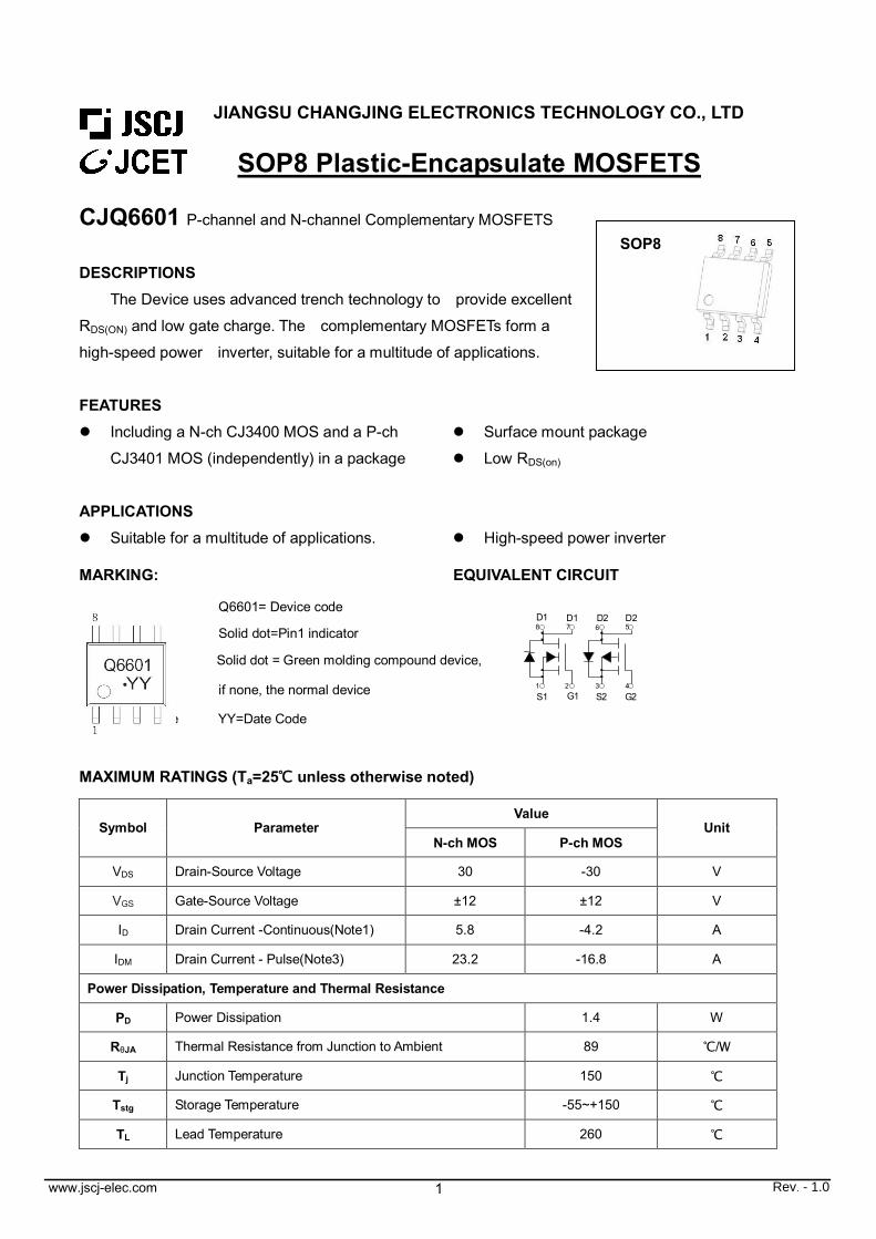
SOP8 SOP8 Plastic-Encapsulate MOSFETS CJQ6601 P-channel and N-channel Complementary MOSFETS DESCRIPTIONS The Device uses advanced trench technology to provide excellent R DS(ON) and low gate charge. The complementary MOSFETs form a high-speed power inverter, suitable for a multitude of applications. FEATURES Including a N-ch CJ3400 MOS and a P-ch CJ3401 MOS (independently) in a package Surface mount package Low R DS(on) APPLICATIONS Suitable for a multitude of applications. High-speed power inverter MARKING: EQUIVALENT CIRCUIT Q6601= Device code Solid dot=Pin1 indicator Solid dot = Green molding compound device, if none, the normal device Front side YY=Date Code MAXIMUM RATINGS (T a =25℃ unless otherwise noted) Value Symbol Parameter N-ch MOS P-ch MOS Unit VDS Drain-Source Voltage 30 -30 V VGS Gate-Source Voltage ±12 ±12 V ID Drain Current -Continuous(Note1) 5.8 -4.2 A IDM Drain Current - Pulse(Note3) 23.2 -16.8 A Power Dissipation, Temperature and Thermal Resistance PD Power Dissipation 1.4 W RθJA Thermal Resistance from Junction to Ambient 89 ℃/W Tj Junction Temperature 150 ℃ Tstg Storage Temperature -55~+150 ℃ TL Lead Temperature 260 ℃ S1 G1 S2 G2 D2 D2 D1 D1 1 2 3 4 5 6 7 8 1 Rev. - 1.0 www.jscj-elec.com JIANGSU CHANGJING ELECTRONICS TECHNOLOGY CO., LTD
Transcript of SOP8 Plastic-Encapsulate MOSFETS sop-8 A-2.pdf · SOP8 SOP8 Plastic-Encapsulate MOSFETS CJQ6601...
SOP8
SOP8 Plastic-Encapsulate MOSFETS
CJQ6601 P-channel and N-channel Complementary MOSFETS
DESCRIPTIONS The Device uses advanced trench technology to provide excellent
RDS(ON) and low gate charge. The complementary MOSFETs form a high-speed power inverter, suitable for a multitude of applications.
FEATURES Including a N-ch CJ3400 MOS and a P-ch
CJ3401 MOS (independently) in a package Surface mount package Low RDS(on)
APPLICATIONS Suitable for a multitude of applications. High-speed power inverter
MARKING: EQUIVALENT CIRCUIT
Q6601= Device code
Solid dot=Pin1 indicator
Solid dot = Green molding compound device,
if none, the normal device
Front side YY=Date Code
MAXIMUM RATINGS (Ta=25 unless otherwise noted)
Value Symbol Parameter
N-ch MOS P-ch MOS Unit
VDS Drain-Source Voltage 30 -30 V
VGS Gate-Source Voltage ±12 ±12 V
ID Drain Current -Continuous(Note1) 5.8 -4.2 A
IDM Drain Current - Pulse(Note3) 23.2 -16.8 A
Power Dissipation, Temperature and Thermal Resistance
PD Power Dissipation 1.4 W
RθJA Thermal Resistance from Junction to Ambient 89 /W
Tj Junction Temperature 150
Tstg Storage Temperature -55~+150
TL Lead Temperature 260
S1 G1 S2 G2
D2D2D1D1
1 2 3 4
5678
1 Rev. - 1.0www.jscj-elec.com
JIANGSU CHANGJING ELECTRONICS TECHNOLOGY CO., LTD
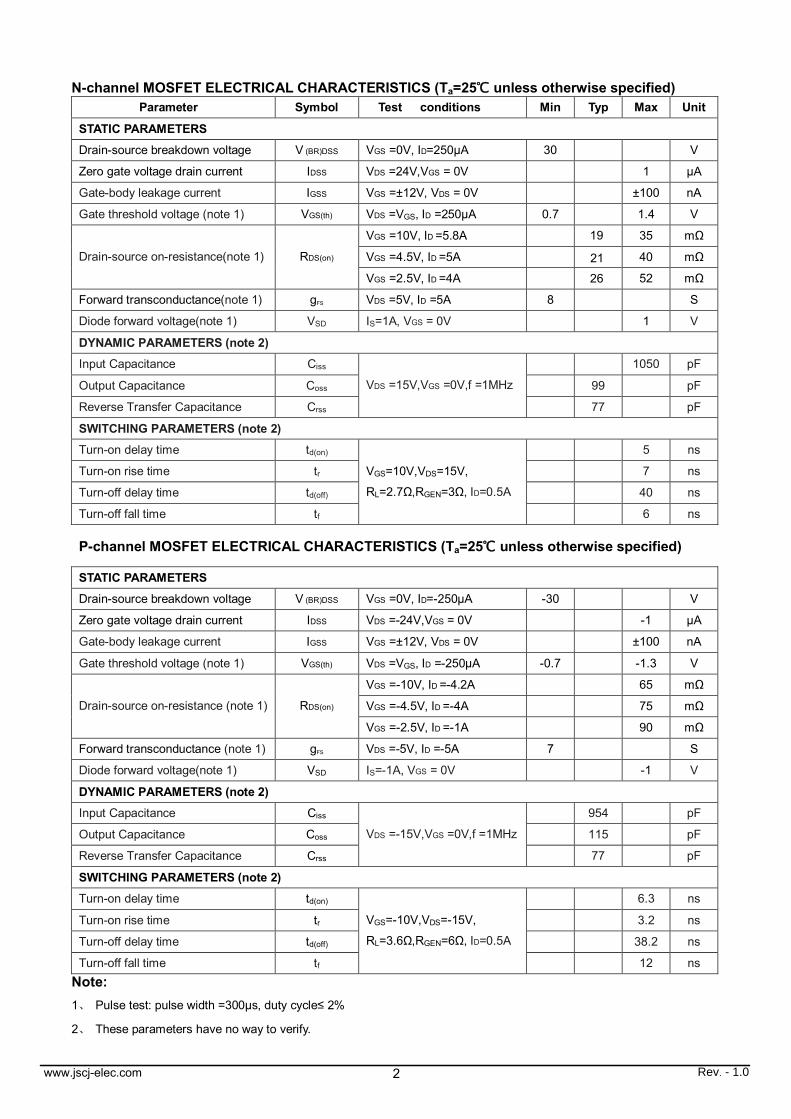
N-channel MOSFET ELECTRICAL CHARACTERISTICS (Ta=25 unless otherwise specified) Parameter Symbol Test conditions Min Typ Max Unit
STATIC PARAMETERS
Drain-source breakdown voltage V (BR)DSS VGS =0V, ID=250µA 30 V
Zero gate voltage drain current IDSS VDS =24V,VGS = 0V 1 µA
Gate-body leakage current IGSS VGS =±12V, VDS = 0V ±100 nA
Gate threshold voltage (note 1) VGS(th) VDS =VGS, ID =250µA 0.7 1.4 V
VGS =10V, ID =5.8A 35 mΩ
VGS =4.5V, ID =5A 40 mΩ Drain-source on-resistance(note 1) RDS(on)
VGS =2.5V, ID =4A 52 mΩ
Forward transconductance(note 1) gFS VDS =5V, ID =5A 8 S
Diode forward voltage(note 1) VSD IS=1A, VGS = 0V 1 V
DYNAMIC PARAMETERS (note 2)
Input Capacitance Ciss 1050 pF
Output Capacitance Coss 99 pF
Reverse Transfer Capacitance Crss
VDS =15V,VGS =0V,f =1MHz
77 pF
SWITCHING PARAMETERS (note 2)
Turn-on delay time td(on) 5 ns
Turn-on rise time tr 7 ns
Turn-off delay time td(off) 40 ns
Turn-off fall time tf
VGS=10V,VDS=15V,
RL=2.7Ω,RGEN=3Ω, ID=0.5A
6 ns
P-channel MOSFET ELECTRICAL CHARACTERISTICS (Ta=25 unless otherwise specified)
STATIC PARAMETERS
Drain-source breakdown voltage V (BR)DSS VGS =0V, ID=-250µA -30 V
Zero gate voltage drain current IDSS VDS =-24V,VGS = 0V -1 µA
Gate-body leakage current IGSS VGS =±12V, VDS = 0V ±100 nA
Gate threshold voltage (note 1) VGS(th) VDS =VGS, ID =-250µA -0.7 -1.3 V
VGS =-10V, ID =-4.2A 65 mΩ
VGS =-4.5V, ID =-4A 75 mΩ Drain-source on-resistance (note 1) RDS(on)
VGS =-2.5V, ID =-1A 90 mΩ
Forward transconductance (note 1) gFS VDS =-5V, ID =-5A 7 S
Diode forward voltage(note 1) VSD IS=-1A, VGS = 0V -1 V
DYNAMIC PARAMETERS (note 2)
Input Capacitance Ciss 954 pF
Output Capacitance Coss 115 pF
Reverse Transfer Capacitance Crss
VDS =-15V,VGS =0V,f =1MHz
77 pF
SWITCHING PARAMETERS (note 2)
Turn-on delay time td(on) 6.3 ns
Turn-on rise time tr 3.2 ns
Turn-off delay time td(off) 38.2 ns
Turn-off fall time tf
VGS=-10V,VDS=-15V,
RL=3.6Ω,RGEN=6Ω, ID=0.5A
12 ns Note: 1、 Pulse test: pulse width =300μs, duty cycle≤ 2%
2、 These parameters have no way to verify.
2 Rev. - 1.0www.jscj-elec.com
19
21 26
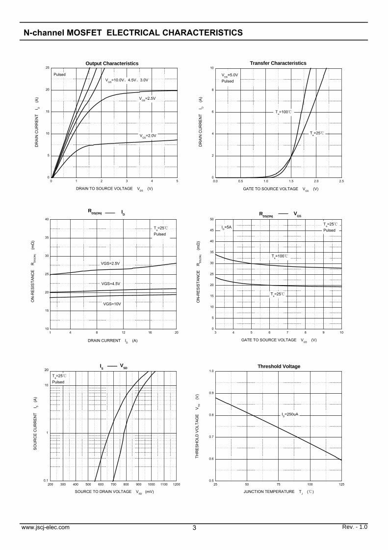
N-channel MOSFET ELECTRICAL CHARACTERISTICS
0 1 2 3 4 50
5
10
15
20
25
3 4 5 6 7 8 9 100
5
10
15
20
25
30
35
40
45
50
0.0 0.5 1.0 1.5 2.0 2.50
2
4
6
8
10
200 300 400 500 600 700 800 900 1000 1100 12000.1
1
10
25 50 75 100 1250.5
0.6
0.7
0.8
0.9
1.0
4 8 12 16 2010
15
20
25
30
35
40
VGS =10.0V、4.5V、3.0V
VGS=2.5V
DR
AIN
CU
RR
ENT
I D
(A
)
DRAIN TO SOURCE VOLTAGE VDS (V)
Pulsed
VGS=2.0V
Ta=100
Ta=25
GATE TO SOURCE VOLTAGE VGS (V)
ON
-RES
ISTA
NC
E
RD
S(O
N)
(mΩ
)
ID=5ATa=25Pulsed
VGS
——RDS(ON)
DR
AIN
CU
RR
ENT
I D
(A
)
GATE TO SOURCE VOLTAGE VGS (V)
VDS=5.0VPulsed
Ta=100
Ta=25
Transfer Characteristics
20
SOU
RC
E C
UR
REN
T
I S (A
)
SOURCE TO DRAIN VOLTAGE VSD (mV)
Ta=25Pulsed
VSDI
S ——
Output Characteristics
THR
ESH
OLD
VO
LTAG
E
V TH
(V)
JUNCTION TEMPERATURE TJ ( )
ID=250uA
Threshold Voltage
VGS=10V
DRAIN CURRENT ID (A)
ON
-RES
ISTA
NC
E
RD
S(O
N)
(mΩ
)
ID——R
DS(ON)
Ta=25Pulsed
VGS=4.5V
VGS=2.5V
1
3 Rev. - 1.0www.jscj-elec.com
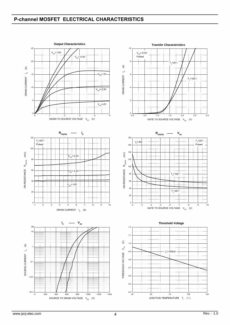
P-channel MOSFET ELECTRICAL CHARACTERISTICS
-0 -1 -2 -3 -4 -5-0
-5
-10
-15
-20
-25
-2 -3 -4 -5 -6 -7 -8 -9 -100
20
40
60
80
100
120
140
160
180
-0 -200 -400 -600 -800 -1000 -1200 -1400-1E-3
-0.01
-0.1
-1
-10
-1 -2 -3 -4 -5 -6 -7 -8 -9 -100
20
40
60
80
100
120
25 50 75 100 125-0.4
-0.5
-0.6
-0.7
-0.8
-0.9
-1.0
-1.1
-1.2
-0.0 -0.5 -1.0 -1.5 -2.0 -2.5 -3.0-0
-2
-4
-6
-8
-10
VGS=-10V
VGS=-4.5V
VGS=-3V
VGS=-2.5V
VGS=-2V
Output Characteristics
DR
AIN
CU
RR
ENT
I D
(A
)
DDAIN TO SOURCE VOLTAGE VDS (V)
Ta=100
Ta=25
Ta=25Pulsed
ID=-4A
—— VGS
RDS(ON)
ON
-RES
IST A
NC
E
RD
S(O
N)
(m
)
GATE TO SOURCE VOLTAGE VGS (V)
VSD——I
S
SOU
RC
E C
UR
REN
T
I S (A
)
SOURCE TO DRAIN VOLTAGE VSD (V)
-20
ID
——RDS(ON)
VGS=-10V
VGS=-2.5V
VGS=-4.5V
Ta=25Pulsed
DRAIN CURRENT ID (A)
ON
-RES
IST A
NC
E
RD
S(O
N)
(m
)
ID=-250uA
Threshold Voltage
THR
ESH
OLD
VO
LTAG
E
V TH
(V)
JUNCTION TEMPERATURE TJ ( )
VDS=-5.0VPulsed
DR
AIN
CU
RR
ENT
I D
(A
)GATE TO SOURCE VOLTAGE VGS (V)
Ta=100
Ta=25
Transfer Characteristics
4www.jscj-elec.com Rev. - 1.0
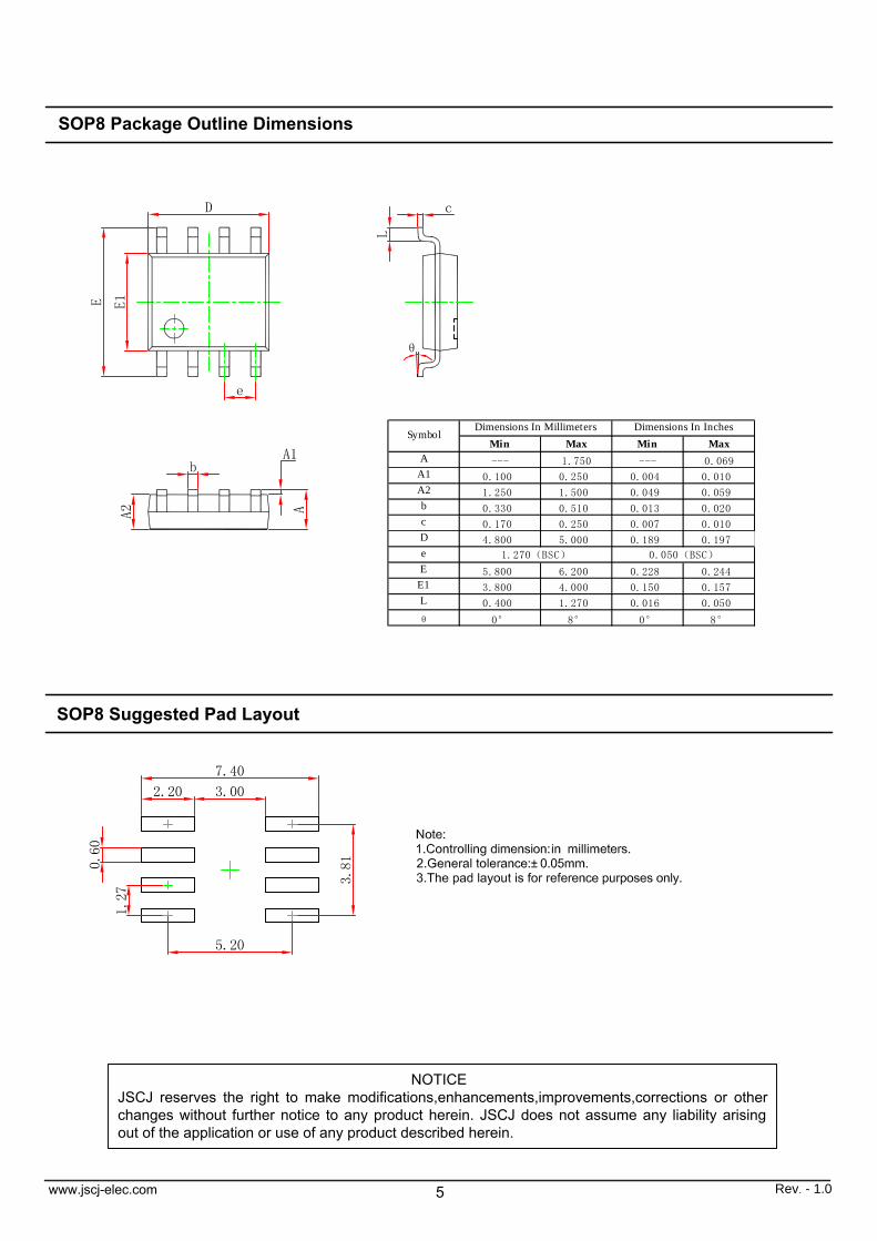
SOP8 Suggested Pad Layout
Min Max Min MaxA --- 1.750 --- 0.069
A1 0.100 0.250 0.004 0.010A2 1.250 1.500 0.049 0.059b 0.330 0.510 0.013 0.020c 0.170 0.250 0.007 0.010D 4.800 5.000 0.189 0.197eE 5.800 6.200 0.228 0.244
E1 3.800 4.000 0.150 0.157L 0.400 1.270 0.016 0.050
θ 0° 8° 0° 8°
SymbolDimensions In Millimeters Dimensions In Inches
0.050(BSC)1.270(BSC)
SOP8 Package Outline Dimensions
5www.jscj-elec.com
NOTICE JSCJ reserves the right to make modifications,enhancements,improvements,corrections or other changes without further notice to any product herein. JSCJ does not assume any liability arising out of the application or use of any product described herein.
Rev. - 1.0
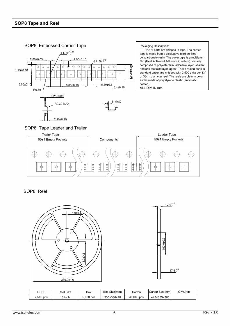
SOP8 Tape and Reel
6www.jscj-elec.com Rev. - 1.0