Solution Manual DSP with FPGAs 1
95
with FPGAs Xilinx HDL Manual 4/e by Dr. Uwe Meyer-Baese Book Webpage: http://www.eng.fsu.edu/~umb Please report bugs to the author’s email : [email protected] ISBN: 0-9755494-6-4
Transcript of Solution Manual DSP with FPGAs 1

with
FPGAs
Xilinx HDL Manual 4/e
by
Dr. Uwe Meyer-Baese
Book Webpage: http://www.eng.fsu.edu/~umb
Please report bugs to the author’s email : [email protected]
ISBN: 0-9755494-6-4
Xilinx HDL Manual DSP with FPGAs/4e
© Dr. Uwe Meyer-Baese 2 all rights reserved
This manual contains the simulation for ModelSim, ISE and Vivado
coding in HDL when using Xilinx tools of the 4. Edition book Digital
Signal Processing with Field Programmable Gate Arrays, published by
Springer Verlag, Heidelberg.
This work is subject to copyright. All right are reserved, whether the
material concerned is used whole or in part, specifically the rights of
translation, reprinting, reuse of illustrations, recitations, broadcastings,
reproduction on microfilm or in any other way, and storage in data banks.
Duplication of this publication or parts thereof is permitted only under the
provisions of the Copyright Law. Permission of use must always be
obtained from the author, Dr. Uwe Meyer-Baese. Violations are liable for
prosecution under the Copyright Law.
1. Printing: August 2015
Xilinx HDL Manual DSP with FPGAs/4e
© Dr. Uwe Meyer-Baese 3 all rights reserved
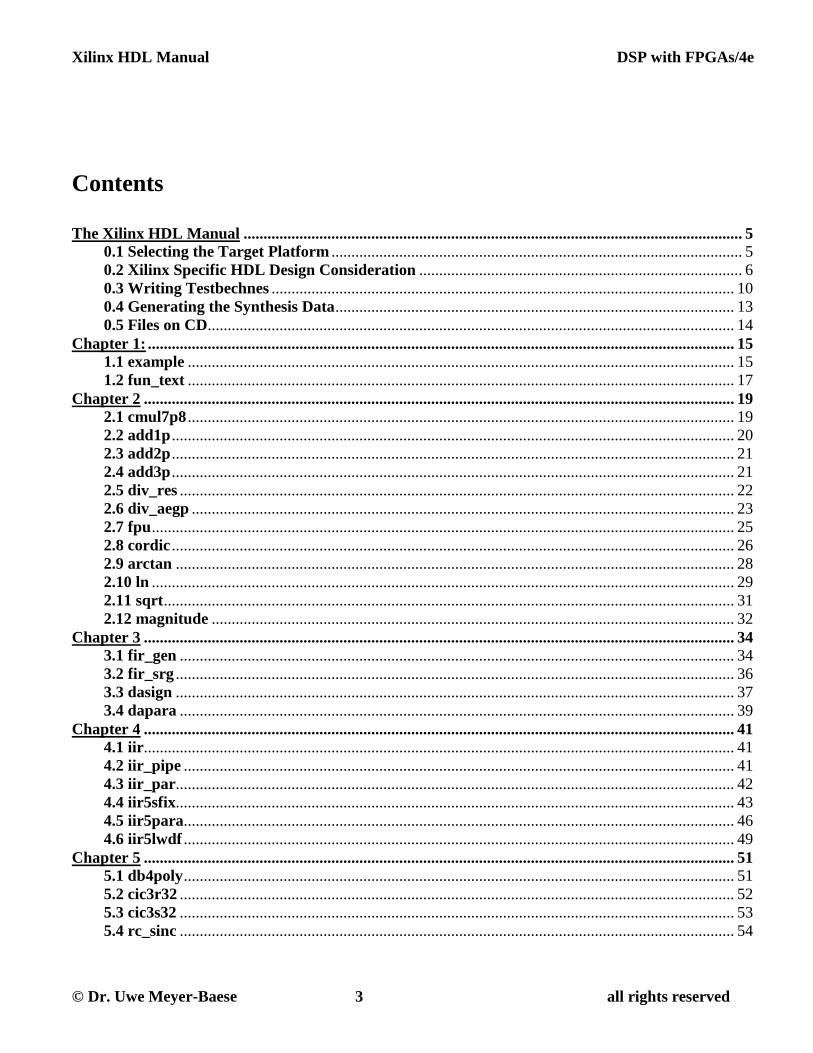
Contents
The Xilinx HDL Manual ............................................................................................................................. 5
0.1 Selecting the Target Platform ....................................................................................................... 5
0.2 Xilinx Specific HDL Design Consideration ................................................................................. 6 0.3 Writing Testbechnes .................................................................................................................... 10 0.4 Generating the Synthesis Data .................................................................................................... 13 0.5 Files on CD.................................................................................................................................... 14
Chapter 1: ................................................................................................................................................... 15 1.1 example ......................................................................................................................................... 15
1.2 fun_text ......................................................................................................................................... 17
Chapter 2 .................................................................................................................................................... 19 2.1 cmul7p8 ......................................................................................................................................... 19 2.2 add1p ............................................................................................................................................. 20 2.3 add2p ............................................................................................................................................. 21
2.4 add3p ............................................................................................................................................. 21 2.5 div_res ........................................................................................................................................... 22
2.6 div_aegp ........................................................................................................................................ 23 2.7 fpu .................................................................................................................................................. 25 2.8 cordic ............................................................................................................................................. 26
2.9 arctan ............................................................................................................................................ 28
2.10 ln .................................................................................................................................................. 29 2.11 sqrt ............................................................................................................................................... 31 2.12 magnitude ................................................................................................................................... 32
Chapter 3 .................................................................................................................................................... 34 3.1 fir_gen ........................................................................................................................................... 34
3.2 fir_srg ............................................................................................................................................ 36 3.3 dasign ............................................................................................................................................ 37
3.4 dapara ........................................................................................................................................... 39
Chapter 4 .................................................................................................................................................... 41 4.1 iir.................................................................................................................................................... 41 4.2 iir_pipe .......................................................................................................................................... 41 4.3 iir_par............................................................................................................................................ 42
4.4 iir5sfix............................................................................................................................................ 43 4.5 iir5para.......................................................................................................................................... 46
4.6 iir5lwdf .......................................................................................................................................... 49
Chapter 5 .................................................................................................................................................... 51 5.1 db4poly .......................................................................................................................................... 51 5.2 cic3r32 ........................................................................................................................................... 52 5.3 cic3s32 ........................................................................................................................................... 53 5.4 rc_sinc ........................................................................................................................................... 54

Xilinx HDL Manual DSP with FPGAs/4e
© Dr. Uwe Meyer-Baese 4 all rights reserved
5.5 farrow ............................................................................................................................................ 55 5.6 cmoms............................................................................................................................................ 57 5.7 db4latti .......................................................................................................................................... 58 5.8 dwtden ........................................................................................................................................... 60
Chapter 6 .................................................................................................................................................... 63 6.1 rader7 ............................................................................................................................................ 63 6.2 fft256.............................................................................................................................................. 64
Chapter 7 .................................................................................................................................................... 73 7.1 lfsr .................................................................................................................................................. 73
7.2 lfsr6s3 ............................................................................................................................................ 73 7.3 ammod ........................................................................................................................................... 74
Chapter 8 .................................................................................................................................................... 75 8.1 fir_lms ........................................................................................................................................... 75
8.2 fir4dlms ......................................................................................................................................... 77 8.3 g711alaw........................................................................................................................................ 78
8.4 adpcm ............................................................................................................................................ 80 8.5 pca.................................................................................................................................................. 82
8.6 ica ................................................................................................................................................... 88
Chapter 9 .................................................................................................................................................... 91 9.1 reg_file ........................................................................................................................................... 91
9.2 trisc0 .............................................................................................................................................. 92

Xilinx HDL Manual DSP with FPGAs/4e
© Dr. Uwe Meyer-Baese 5 all rights reserved
The Xilinx HDL Manual
Field-programmable gate arrays (FPGAs) are revolutionizing digital signal processing. Many front-end
digital signal processing (DSP) algorithms, such as FFTs, multi channel filter banks, or wavelets, to name
just a few, previously built with ASICs or programmable digital signal processors, are now most often
replaced by FPGAs. The two FPGA market leaders (Altera and Xilinx) both report revenues greater than
$1 billion. FPGAs have enjoyed steady growth of more than 20% in the last decade, outperforming ASICs
and programmable digital signal processors (PDSPs) by 10%.
Design of current DSP applications using state-of-the art multi-million gates devices requires a broad
foundation of the engineering skills ranging from knowledge of hardware-efficient DSP algorithms to
CAD design tools. This has been the foundation for the book Digital Signal Processing with Field
Programmable Gate Arrays now available in the 4. Edition [1] that was mainly based on Altera’s Quartus
software and ModelSim simulation via “do” files.
While the design flows for Altera and Xilinx tools are similar there has been some notable difference over
the years. Most visible in the handling of the simulation of the designs. We have seen the two FPGA
market leaders take opposite directions in recent years. In the past Altera favored the internal VWF
waveform simulator (up to Quartus II version 9.1) and now recommends the external ModelSim-
Altera or Qsim. Xilinx on the other hand, since version 12.3 (end of 2010), no longer provides a free
ModelSim simulator and instead provides a free embedded ISIM simulator that is integrated within
the ISE Tool and the Vivado tool has a similar internal simulator called XSIM too. The two main obvious
differences are that the ISIM simulator has the option to do a simulation via TCL script, while the XSIM
simulator has an analog (aka waveform) display option. The simulator considerations for ISIM and
Vivado is discussed later in more detail in section 0.2.
The Altera Quartus II software comes with two free simulator options. The ModelSim-Altera allows
us to use the professional tool from Mentor Graphic Inc. The second alterative is the Altera Qsim tool that
may have a few less feature than ModelSim (e.g., no analog waveform) but is also a little easier to
handle since is does not require one to write HDL test benches or DO file scripts to assign I/O signals.
However, at the time of writing of the book [1] the Qsim in 12.1 did not support the Cyclone IV devices
and therefore the ModelSim-Altera was selected as default simulator. Moving between VHDL and
Verilog stimuli file and Altera and Xilinx was also simplified by using ModelSim-Altera DO files
and not HDL test benches.
0.1 Selecting the Target Platform
If we like to select an appropriate Xilinx FPGA platform for all designs, then we need to provide enough
resources (LE, embedded multipliers, Block RAMs, and number of pins) to host the largest designs. On
the other side we may want to select a (low cost) board that is available through Xilinx University
program (ZedBoard, Zybo, Nexys 4, Basys, or Atlys as of 7/2015) which are designed by Digilent Inc.
and are provided at low cost even for non-university customers. Another goal maybe to use boards that are
supported by the Vivado web edition software. As of 7/2015 the ZedBoard, Zynq and an Artix-7 board are
supported in the Vivado web edition. Table 0.1 gives an overview of some popular boards.

Xilinx HDL Manual DSP with FPGAs/4e
© Dr. Uwe Meyer-Baese 6 all rights reserved
Table 0.1: Overview of popular Xilinx boards, their FPGAs and resources.
Board Device Avail. I/O LUT DSP BRAMs
ZYBO xc7z010t-1clg400 100 17,600 80 60
ZedBoard xc7z020clg484-1 200 53,200 220 140
Artix-7 xc7a200tfbg676-2 400 134,600 740 365
Kintex-7 xc7k325ffg900-2 500 203,800 840 1335
Virtex-7 xc7vx485ffg1761-2 700 303,600 2800 3090
The maximum values for all Altera DE2 examples in [1] were 33,926 LEs, 184 multipliers 9x9, 2 Block
RAMs, and 413 pins. There are only 4 designs with more than 200 pins, and many of the I/Os have been
used for monitoring and placed in the I/O section to guarantee that this signals are observable. Many of
these signals are not essential for the function. The fft256 design for instance has a total of 413 pins,
however, essential for the function are only: clk, reset, xr_in, xi_in, fft_valid, fftr
and ffti, which account for 3+4x16=67 pins that would fit even on the smallest board from Table 0.1.
The timing simulation will require a full compile such that all timing is available depends in part on the
FPGA size. Considerable compile time can be saved (about 50%) if we use a “quick” compile strategy
with less optimization as Table 0.2 shows. Compile time in general even with a big device is still
reasonable for the Vivado tool.
Table 0.2: Compile time for a few typical boards and compile options for the fun_text design.
Synthesis alone took about 30 sec (device independent). (i7 PC; 12 GB; Win8.1;Vivado 2015.1)
Board Option Time
Artix Board Standard synthesis 2:23
Artix Board Quick flow 1:19
Zedboard Standard synthesis 1:37
Zedboard Quick flow 1:08
Big FPGA Xc7a2000 with 500 I/O Quick flow 1:15
Biggest Zynq xc7z030 Quick flow 1:10
0.2 Xilinx Specific HDL Design Consideration
Xilinx has announce that in the future the Vivado tool set will be supported and the ISE tool set will be
retired. Unfortunately, Vivado seemed not to support any FPGA family before the 7. generation and many
designer if using e.g. Virtex-6 devices will have to continue to use the ISE tools still. In the last two years
since introducing the Vivado software in 2013 no effort has been seen to support older FPGA devices in
Vivado. We will therefore briefly discuss the ISE simulation flow but will use whenever possible the
Vivado tool in the compile file listing.
When simulating a design with the ISIM simulator we have the option to use a stimuli file from a TCL
script similar to ModelSim DO files, or we can write a test bench in HDL. A test bench is a short HDL
file, where we instantiate the circuit to be tested and then generate and apply our test signals with a
statement like
clk <= NOT clk AFTER 5 ns;

Xilinx HDL Manual DSP with FPGAs/4e
© Dr. Uwe Meyer-Baese 7 all rights reserved
Fig. 0.1: Behavior simulation with no GSR consideration. Note that the accumulator
starts at the 0 ns time marker.
to generate a clock with a 2 x 5ns = 10 ns clock period. However, one difficulty with the ISIM test bench
comes from the fact that the circuit with timing information (i.e., *_timesim.vhd) is synthesized
directly from the netlist and the STD_LOGIC is used throughout the whole ENTITY description. The
original ENTITY data types and GENERIC variables are ignored. If we like to use the same VHDL test
bench for RTL and timing simulation then the ENTITY will be restricted to a single data type. More
precise, we cannot use INTEGER, SIGNED, or FLOAT data types, and even BUFFER or GENERIC
parameter would not be permitted. This can be considered a great interference with the coding for design
reuse and we would need to use a separate test bench for RTL and timing simulation. However, if we do
not use a test bench and simulate our circuit directly using the TCL stimuli script, then we can use the
same script for RTL and timing simulation. Furthermore, for VHDL and Verilog the same stimuli file can
be used; only the compile sequence will be different. The ISIM TCL scripts and ModelSim DO files are
also very similar in their coding style to simplify a transition between the two simulators.
Similar restrictions apply for the Vivado XSIM simulation. Here in general a Verilog netlist on LUT-
based level is used to have accurate timing simulation. Since a Verilog netlist is used even for VHDL
designs a match with VHDL source code is only possible for STD_LOGIC or STD_LOGIC_VECTOR and
BOOLEAN type. Again we cannot use INTEGER, SIGNED, or FLOAT data types, and even BUFFER or
GENERIC parameter are not be permitted. However, this applies only to the I/O interface. Within the
design we can indeed use INTEGERs, and design reuse with GENERIC parameters, can be done in
VHDL via CONSTANT definitions and as PARAMETER in Verilog within the designs without interference
the coding requirements for the I/O ports of the designs.

Xilinx HDL Manual DSP with FPGAs/4e
© Dr. Uwe Meyer-Baese 8 all rights reserved
Fig. 0.2: Timing simulation with no GSR consideration. Note that the accumulator starts after the
100 ns time marker. This results in a behavior/timing simulation mismatch.
Another important design consideration for the Xilinx tools is the handling of the Global set/reset (GSR)
in the simulator. The idea behind the GSR is that all flip-flops in all FPGAs are set to predefined values
after reset within the first 100 ns of the simulation. Only after the first 100 ns any flip-flop operation can
occur. Generated timing netlist will always ensure this functionality, however, the behavior simulation
does not necessary follows this by default. This is demonstrated by the function generator simulator
shown in Figure 0.1 and 0.2. The function generator designed as an accumulator followed by a sine wave
LUT. As can be seen in the behavior simulation (Fig. 0.1) the sine wave starts earlier than the timing
simulation due to the 100 ns GSR in the timing simulation, see Fig 0.2. To avoid such a mismatch in the
behavior/timing simulation it is therefore highly recommended to hold flip-flop activity via a ENABLE or
RESET signal for the first 100 ns as shown in Fig. 0.3. This timing simulation can then be matched with a
behavior simulation with a 100 ns reset, see Fig. 0.4.

Xilinx HDL Manual DSP with FPGAs/4e
© Dr. Uwe Meyer-Baese 9 all rights reserved
Fig. 0.3: Timing simulation with GSR consideration. Note that the accumulator starts after the 100ns
time marker to match the behavior simulation due to the long 100 ns active reset.

Xilinx HDL Manual DSP with FPGAs/4e
© Dr. Uwe Meyer-Baese 10 all rights reserved
0.3 Writing Testbenches
With today’s high complex designs a substantial design effort is directed towards the verification of the
circuit. As the Pentium bug in the FP divider hardware has shown us in 1995, such an insufficient testing
can have a large financial impact (over $100M for Intel) besides the image damage such a recall may
have.
Verification can take many different forms. For a small design we can use the “RTL viewer” aka “System
view” to inspect the synthesized circuit. For a more complicated system we may use input test stimuli
generated on the fly or via a test vector look-up table generated in MatLab or with a C/C++ program. The
correct output behavior can be text-based, i.e. report “mismatch” of actual and expected results, or
graphical such as an oscilloscope, see Fig. 0.5.
Fig. 0.4: Behavior simulation with GSR consideration for first 100 ns. Note that the behavior
simulation should not show any flip-flop behavior within the first 100 ns using a RESET or ENABLE
signal. This allows a match in a behavior/timing simulation.

Xilinx HDL Manual DSP with FPGAs/4e
© Dr. Uwe Meyer-Baese 11 all rights reserved
Writing a text-based HDL testbench (TB) is not too complicated but nevertheless can be labor intensive.
Until ISE 11 Xilinx offered a tool call “HDL Bencher.” You had to define waveform for input signals,
and you could specify or generate the desired results based on a behavior simulation. This tools is still
available at www.xilinx.com/webpack/classics/wpclassic as of 7/2105, see Fig. 0.6 for an example [2].
On the other side you may have special requirements how a TB should look like and then in general it is
preferred to use such a template as starting point [3]. A template typically will have the following
elements:
1. Libraries in use such as IEEE
2. An “empty” entity without any ports
3. The “Unit Under Test” (UUT) component definition
4. The signals/wires/reg in use
5. The UUT component instantiation
6. Definition of period signals, e.g., clk
7. Definition of a-period data signals, e.g., reset, data input etc.
The Verilog TB will not have item 1 and 3. It also important to remember that the XSIM simulator orders
the displayed signals by default as specified item under 4, in precisely the shown order. I.e., in order to
avoid rearranging the signals in the simulator window it is recommended to sort the signals/reg/wires in
the order we like to see them in the waveform window. The simulator does not care about the ordering of
the components port or the order how you assign the ports in the component instantiation. Vivado Verilog
and VHDL simulation will look in general very similar. Only in case we have used VHDL FSM state
coding with literal names this will in Verilog be displayed as integer numbers since a literal display is not
supported in Verilog simulation.
In case large input data sets are needed (e.g. designs DWTDEN, PCA, or ICA) the input data can be stored
in a CONSTANT array, e.g.:
TYPE rom_type IS ARRAY (0 TO 1023) OF STD_LOGIC_VECTOR(15 DOWNTO 0); CONSTANT rom : rom_type := (
X"04a9",X"0282",X"004d",X"0168",X"fd37",X"06c9",X"003c",X"0730",X"010e",X"037d",
X"fa37",X"fd32",X"04fc",X"fd72",X"024f",X"0a8f",X"0b75",X"069a",X"06eb",X"0ff0",
…
Fig. 0.5: Testbench design.

Xilinx HDL Manual DSP with FPGAs/4e
© Dr. Uwe Meyer-Baese 12 all rights reserved
In Verilog we can use a Verilog ROM definition, e.g.
reg [15:0] ROM [639:0];
assign data = ROM[addr];
initial begin
ROM[0]=16'h0000;
ROM[1]=16'h04a9;
ROM[2]=16'h0282;
ROM[3]=16'h004d;
…
Or we can take advantage of them Verilog memread function
initial // Data read alternative via readmem
begin
$readmemh("dcf77.mif", rom);
end
Of course we have to add the divider and the text by hand after we have start the Vivado behavior or
timing simulation.
(a) (b)
Fig. 0.6: The HDL bencher provide by ISE until version 11. (a) Testbench desired values and simulation
results. (b) Error message for mismatch using ModelSim simulation at time 115 ns. Value desired was
specified as decimal 50 but the simulation shows a value of decimal 51.

Xilinx HDL Manual DSP with FPGAs/4e
© Dr. Uwe Meyer-Baese 13 all rights reserved
0.4 Generating the Synthesis Data
A full set of synthesis data in general will require a device specification and a full compile that can take up
substantial CPU time for a big device. The map report will show the desired values such as the number of
flip-flop, LUT, I/O, Bufg, block RAMs and embedded multipliers used. Since device families have
different type of logic cells, LUT and block RAM sizes this data may vary for different devices.
The ISE software will allow us to set optimization Goal to “Speed” or “Area” by a right click on
“Synthesize – XST” the Process properties dialog will pop up and the –opt_mode switch can be
defined. After a full compile ISE will provide maximum clock frequency or minimum period required
from the “Post-Par Static Timing Report.”
The Vivado software in the “Project Manager” view will have an excellent overview of the implemented
design. It will not only show the files and library used and resources in bar graph or table form, also power
dissipation and timing information are shown in the “Project Summary” window, a substantial
improvement to the ISE software, that has all this information too just more buried in the report files.
To get the timing data, however, Vivado has no longer the “Speed” or “Area” option as ISE, instead we
need to constrain the design. The idea comes from the Synopsys ASIC constrain files, where you specify a
desired clock frequency and if the synthesis reaches the clock goal, the rest of the compile effort can be
directed to reducing the area of the design. At a minimum we need to specific a constrain file *.xdc and
set the clock as follows:
create_clock -period 10 -name clk [get_ports clk]
where clk is assumed the name of the clock signal. This will set the desired clock period to 10 ns, or 100
MHz. If that frequency is too high for the device chosen, then a negative clock skew is reported and we
need to increase the period. Finding the maximum speed is therefore an iterative process, more labor
intensive than with ISE. Finding a “Area” optimum is simple, we just relax the timing requirement, to say
–period 1000 (i.e., 1 MHz clock) and all effort of the compiler will be used to minimize the area.

Xilinx HDL Manual DSP with FPGAs/4e
© Dr. Uwe Meyer-Baese 14 all rights reserved
0.5 Files on CD
The files on the CD include a full set of 45 VHDL and 44 Verilog projects for all examples for the book
Digital Signal Processing with Field Programmable Gate Arrays from the 4. Edition [1]. Each of the
project’s has at least the following VHDL files in directory vivado:
project.vhd Original VHDL design with Xilinx I/O interface for data type and generics
project.do ModelSim VHDL stimuli files for design with GSR delay
project_tb.vhd The 7 section VHDL testbench file including data stimuli
project_tb.do ModelSim stimuli files for testbench with GSR delay and no data stimuli
project_tb_msim.gif The snapshot of the VHDL ModelSim TB simulation
Only for the FPU an ISIM timing simulation had been added since the XSIM simulation did not show the
expected results. In total you will find over 250 files in the VHDL folder. The Verilog files in directory
vvivado are:
project.v Original Verilog design with Xilinx I/O parameter
project.do ModelSim Verilog stimuli files for design with GSR delay
project_tb.v The 5 section Verilog testbench file including data stimuli
project_tb.do ModelSim stimuli file for testbench with GSR delay and no data stimuli
project_vtb_msim.gif The snapshot of the Verilog ModelSim TB simulation
project_vtb_behav.gif The snapshot of the Verilog behavior Vivado TB simulation
project_vtb_behav.wcfg The waveform file of the Verilog behavior Vivado TB simulation
project_vtb_time.gif The snapshot of the Verilog timing Vivado TB simulation
project_vtb_time.wcfg The waveform file of the Verilog timing Vivado TB simulation
In total you will find over 420 files in the Verilog folder. Only a few designs needed additional files such
as memory initializations (e.g., fun_text or fft256) and some need longer input testbench data
such as dwtden, ica, or pca.
REFERENCES
[1] U. Meyer-Baese, “Digital Signal Processing with Field Programmable Gate Arrays”, Springer,
Heidelberg 2015.
[2] Visual Software Solutions, Inc. “HDL Bencher User’s Guide” 60 pages.
[3] M. Hamid, “Writing Efficient Testbenches”, Xilinx XAAP199, May 2010.

Xilinx HDL Manual DSP with FPGAs/4e
© Dr. Uwe Meyer-Baese 15 all rights reserved
Chapter 1:
1.1 example
(a)
(b)

Xilinx HDL Manual DSP with FPGAs/4e
© Dr. Uwe Meyer-Baese 16 all rights reserved
(c)
Fig. 1.1: Simulation for example. The example code shows different HDL coding styles such as data
flow (concurrent), sequential, and component instantiations, see Fig. 1.25 in 4/e. (a) VHDL ModelSim
simulation. (b) Vivado Verilog behavior simulation. (c) Vivado Verilog timing simulation.

Xilinx HDL Manual DSP with FPGAs/4e
© Dr. Uwe Meyer-Baese 17 all rights reserved
1.2 fun_text
(a)

Xilinx HDL Manual DSP with FPGAs/4e
© Dr. Uwe Meyer-Baese 18 all rights reserved
(b)
(c)
Fig. 1.2: Simulation for fun_text. The fun_text code shows an implementation of a sine wave
generation using accumulator followed by a ROM look-up table. (a) VHDL ModelSim simulation. (b)
Vivado Verilog behavior simulation. (c) Vivado Verilog timing simulation.

Xilinx HDL Manual DSP with FPGAs/4e
© Dr. Uwe Meyer-Baese 19 all rights reserved
Chapter 2
2.1 cmul7p8
(a)
(b)
(c)
Fig. 2.1: Simulation for cmul7p8. The evaluation is from left to right and the quantization error is larger
Xilinx HDL Manual DSP with FPGAs/4e
© Dr. Uwe Meyer-Baese 20 all rights reserved
if the division (and rounding) is done first. (a) VHDL ModelSim simulation. (b) Vivado Verilog
behavior simulation. (c) Vivado Verilog timing simulation.
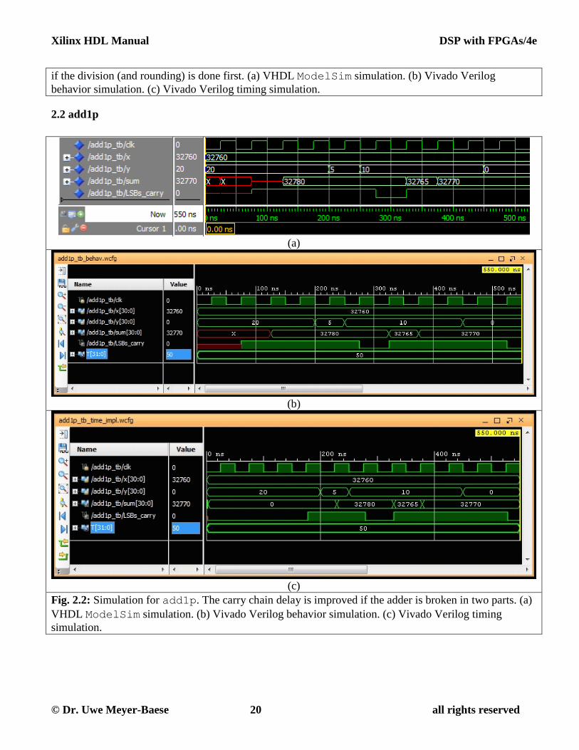
2.2 add1p
(a)
(b)
(c)
Fig. 2.2: Simulation for add1p. The carry chain delay is improved if the adder is broken in two parts. (a)
VHDL ModelSim simulation. (b) Vivado Verilog behavior simulation. (c) Vivado Verilog timing
simulation.

Xilinx HDL Manual DSP with FPGAs/4e
© Dr. Uwe Meyer-Baese 21 all rights reserved
2.3 add2p
(a)
(b)
(c)
Fig. 2.3: Simulation for add2p. With two pipeline stages the adder is broken into three parts. (a) VHDL
ModelSim simulation. (b) Vivado Verilog behavior simulation. (c) Vivado Verilog timing simulation.
2.4 add3p
(a)

Xilinx HDL Manual DSP with FPGAs/4e
© Dr. Uwe Meyer-Baese 22 all rights reserved
(b)
(c)
Fig. 2.4: Simulation for add3p. With three pipeline stages the adder can be broken into 4 parts. (a) VHDL
ModelSim simulation. (b) Vivado Verilog behavior simulation. (c) Vivado Verilog timing simulation.
2.5 div_res
(a)

Xilinx HDL Manual DSP with FPGAs/4e
© Dr. Uwe Meyer-Baese 23 all rights reserved
(b)
(c)
Fig. 2.5: Simulation for div_res. Division using the restoring principle, i.e., if a partial result is
negative a correction is done to produce a positive restored value. (a) VHDL ModelSim simulation. (b)
Vivado Verilog behavior simulation. (c) Vivado Verilog timing simulation. The local variable “r” is not
available in the timing simulation.
2.6 div_aegp
(a)

Xilinx HDL Manual DSP with FPGAs/4e
© Dr. Uwe Meyer-Baese 24 all rights reserved
(b)
(c)
Fig. 2.6: Simulation for div_aegp. Division using the method from Anderson, Earle, Goldschmidt, and
Powers for 1.5/1.2 using a finite state machine with three processing steps sufficient for 8-bit precision. (a)
VHDL ModelSim simulation. (b) Vivado Verilog behavior simulation. (c) Vivado Verilog timing
simulation. The Verilog simulations (b/c) show integer values for the machine state while VHDL (a) uses
literate coding.

Xilinx HDL Manual DSP with FPGAs/4e
© Dr. Uwe Meyer-Baese 25 all rights reserved
2.7 fpu
(a)
(b)
(c)

Xilinx HDL Manual DSP with FPGAs/4e
© Dr. Uwe Meyer-Baese 26 all rights reserved
(d)
Fig. 2.7: Simulation of the design fpu. The design uses the ieee_proposed library by David Bishop.
Eight basic floating point operations are applied to the input values 1/3 and 2/3 as shown in the “op” row
in the VHDL simulation. (a) VHDL ModelSim simulation. (b) Vivado VHDL behavior simulation. (c)
Vivado VHDL timing simulation with errors. (d) ISIM VHDL timing simulation. Note that the Vivado
timing simulation shows errors. Currently there is no equivalent library available for Verilog designs.
2.8 cordic
(a)

Xilinx HDL Manual DSP with FPGAs/4e
© Dr. Uwe Meyer-Baese 27 all rights reserved
(b)
(c)
Fig. 2.8: Simulation for cordic. Two data (x=-41 and y=55) are transformed from Cartesian to polar

Xilinx HDL Manual DSP with FPGAs/4e
© Dr. Uwe Meyer-Baese 28 all rights reserved
representation that yield radius (r=111) and phase (phi=123). The error is eps=9. This is a pipelined
implementation and the rotation can be monitored in the behavior simulation. (a) VHDL ModelSim
simulation. (b) Vivado Verilog behavior simulation. (c) Vivado Verilog timing simulation. The
pipeline register “x” and “y” are not visible in the Vivado timing simulation (c).
2.9 arctan
(a)
(b)

Xilinx HDL Manual DSP with FPGAs/4e
© Dr. Uwe Meyer-Baese 29 all rights reserved
(c)
Fig. 2.9: Simulation for arctan. For five values: 0, ±0.5, ±1 the arctan function is computed using a
Chebyshev approximation. (a) VHDL ModelSim simulation. (b) Vivado Verilog behavior simulation. (c)
Vivado Verilog timing simulation.
2.10 ln
(a)

Xilinx HDL Manual DSP with FPGAs/4e
© Dr. Uwe Meyer-Baese 30 all rights reserved
(b)
(c)
Fig. 2.10: Simulation for ln. For five values: 0, 0.25, 0.5, 0.75, and 1.0 the natural logarithm function is
computed using a Chebyshev approximation. (a) VHDL ModelSim simulation. (b) Vivado Verilog
behavior simulation. (c) Vivado Verilog timing simulation.

Xilinx HDL Manual DSP with FPGAs/4e
© Dr. Uwe Meyer-Baese 31 all rights reserved
2.11 sqrt
(a)
(b)

Xilinx HDL Manual DSP with FPGAs/4e
© Dr. Uwe Meyer-Baese 32 all rights reserved
(c)
Fig. 2.11: Simulation for sqrt. The input value x =0.75/8 =3072/32768 is first normalized and the square
root is compute using a finite state machine with a final post processing operation. The Verilog simulation
shows plain number instead of literal for the machine state. (a) VHDL ModelSim simulation. (b) Vivado
Verilog behavior simulation. (c) Vivado Verilog timing simulation. The local signal “op” cannot be found
in the timing netlist.
2.12 magnitude
(a)

Xilinx HDL Manual DSP with FPGAs/4e
© Dr. Uwe Meyer-Baese 33 all rights reserved
(b)
(c)
Fig. 2.12: Simulation for magnitude. The magnitude is approximated by the equation
max(x,y)+min(x,y)/4 and tested for 9 angles at k*π/4. (a) VHDL ModelSim simulation. (b) Vivado
Verilog behavior simulation. (c) Vivado Verilog timing simulation.

Xilinx HDL Manual DSP with FPGAs/4e
© Dr. Uwe Meyer-Baese 34 all rights reserved
Chapter 3
3.1 fir_gen
(a)

Xilinx HDL Manual DSP with FPGAs/4e
© Dr. Uwe Meyer-Baese 35 all rights reserved
(b)
(c)
Fig. 3.1: Simulation for fir_gen. This is a generic FIR filter design that allows to load first different
coefficients and then after Load_x goes high performs filtering. In the example a length four filter is
simulated with Daubechies length 4 wavelet filter coefficients. (a) VHDL ModelSim simulation. (b)
Vivado Verilog behavior simulation. (c) Vivado Verilog timing simulation. The local variables “x, c, p”

Xilinx HDL Manual DSP with FPGAs/4e
© Dr. Uwe Meyer-Baese 36 all rights reserved
and “a” are not available in the timing simulation.
3.2 fir_srg
(a)
(b)

Xilinx HDL Manual DSP with FPGAs/4e
© Dr. Uwe Meyer-Baese 37 all rights reserved
(c)
Fig. 3.2: Simulation for fir_srg. A length four filter with coefficients -1,3.75,3.75,-1 is used. This is a
starting point design that can be further optimized by using coefficient symmetry, CSD coding, and
pipelining. (a) VHDL ModelSim simulation. (b) Vivado Verilog behavior simulation. (c) Vivado Verilog
timing simulation. The local variable “tap” is not available in the timing simulation.
3.3 dasign
(a)

Xilinx HDL Manual DSP with FPGAs/4e
© Dr. Uwe Meyer-Baese 38 all rights reserved
(b)
(c)
Fig. 3.3: Simulation for dasign. A signed distributed arithmetic sum-of-product computation is
simulated for three coefficients {-2,3,1} three input word x={1,-3,7}with each having 4 bits. (a) VHDL
ModelSim simulation. (b) Vivado Verilog behavior simulation. (c) Vivado Verilog timing simulation.
The local variables “x2[0], x1[0],x0[0]” and “p” are not available in the timing simulation.

Xilinx HDL Manual DSP with FPGAs/4e
© Dr. Uwe Meyer-Baese 39 all rights reserved
3.4 dapara
(a)
(b)

Xilinx HDL Manual DSP with FPGAs/4e
© Dr. Uwe Meyer-Baese 40 all rights reserved
(c)
Fig. 3.4: Simulation for dapara. This is a parallel implementation of the distributed arithmetic sum-of-
product computation. The design has three coefficients {-2,3,1} and three input word x={1,-3,7} each
having 4 bits. (a) VHDL ModelSim simulation. (b) Vivado Verilog behavior simulation. (c) Vivado
Verilog timing simulation. The local variables “x[0],x[1],x[2]” and “x[3]” are not available in the timing
simulation.

Xilinx HDL Manual DSP with FPGAs/4e
© Dr. Uwe Meyer-Baese 41 all rights reserved
Chapter 4
4.1 iir
(a)
(b)
(c)
Fig. 4.1: Simulation of the filter response to an impulse 1000 for iir is shown. This is a first order IIR
filter with a pole at z=0.75. (a) VHDL ModelSim simulation. (b) Vivado Verilog behavior simulation. (c)
Vivado Verilog timing simulation. For Verilog a negative impulse was used to verify the correct sign
extensions.
4.2 iir_pipe
(a)

Xilinx HDL Manual DSP with FPGAs/4e
© Dr. Uwe Meyer-Baese 42 all rights reserved
(b)
(c)
Fig. 4.2: Simulation for iir_pipe. This is a look-ahead pipelined lossy integrator with an effective pole
at z=0.75. The response to an impulse 1000 of the IIR first order filter is shown. (a) VHDL ModelSim
simulation. (b) Vivado Verilog behavior simulation. (c) Vivado Verilog timing simulation.
4.3 iir_par
(a)

Xilinx HDL Manual DSP with FPGAs/4e
© Dr. Uwe Meyer-Baese 43 all rights reserved
(b)
(c)
Fig. 4.3: Simulation for iir_par. This is a parallel implementation of the IIR filter with a pole at
z=0.75. The response to an impulse 1000 of the first order IIR filter is shown. (a) VHDL ModelSim
simulation. (b) Vivado Verilog behavior simulation. (c) Vivado Verilog timing simulation. The local
variable “state” is not available in the timing simulation.
4.4 iir5sfix

Xilinx HDL Manual DSP with FPGAs/4e
© Dr. Uwe Meyer-Baese 44 all rights reserved
(a)

Xilinx HDL Manual DSP with FPGAs/4e
© Dr. Uwe Meyer-Baese 45 all rights reserved
(b)

Xilinx HDL Manual DSP with FPGAs/4e
© Dr. Uwe Meyer-Baese 46 all rights reserved
(c)
Fig. 4.4: Simulation of the impulse response for iir5sfix. This is a 5. order direct form IIR filter design that
was implemented using the sfixed type in VHDL and without special data type in Verilog. (a) VHDL
ModelSim impulse response. (b) Vivado Verilog behavior simulation. (c) Vivado Verilog timing simulation.
4.5 iir5para
(a)

Xilinx HDL Manual DSP with FPGAs/4e
© Dr. Uwe Meyer-Baese 47 all rights reserved
(b)

Xilinx HDL Manual DSP with FPGAs/4e
© Dr. Uwe Meyer-Baese 48 all rights reserved
(c)
Fig. 4.5: Simulation of a step response for iir5para. This is a 5. order parallel implementation of a
narrow band IIR filter design that was implemented using the sfixed type in VHDL and without special
data type in Verilog. (a) VHDL ModelSim step response. (b) Vivado Verilog behavior simulation. (c)
Vivado Verilog timing simulation.

Xilinx HDL Manual DSP with FPGAs/4e
© Dr. Uwe Meyer-Baese 49 all rights reserved
4.6 iir5lwdf
(a)
(b)
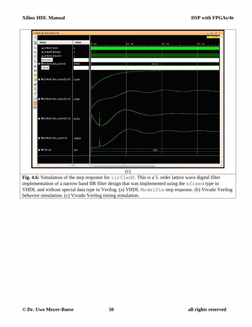
Xilinx HDL Manual DSP with FPGAs/4e
© Dr. Uwe Meyer-Baese 50 all rights reserved
(c)
Fig. 4.6: Simulation of the step response for iir5lwdf. This is a 5. order lattice wave digital filter
implementation of a narrow band IIR filter design that was implemented using the sfixed type in
VHDL and without special data type in Verilog. (a) VHDL ModelSim step response. (b) Vivado Verilog
behavior simulation. (c) Vivado Verilog timing simulation.

Xilinx HDL Manual DSP with FPGAs/4e
© Dr. Uwe Meyer-Baese 51 all rights reserved
Chapter 5
5.1 db4poly
(a)
(b)

Xilinx HDL Manual DSP with FPGAs/4e
© Dr. Uwe Meyer-Baese 52 all rights reserved
(c)
Fig. 5.1: Simulation for db4poly. A polyphase decomposition is demonstrated for the length 4
Daubechies filter. The triangular input shows the splitting in even and odd inputs and the impulse of 100
at even and odd index inputs shows the “not time invariant” behavior of the system. (a) VHDL
ModelSim simulation. (b) Vivado Verilog behavior simulation. (c) Vivado Verilog timing simulation.
The local variable “state” is not available in the Vivado simulation, but clk2 can be used as
representation for the state variable.
5.2 cic3r32
(a)

Xilinx HDL Manual DSP with FPGAs/4e
© Dr. Uwe Meyer-Baese 53 all rights reserved
(b)
(c)
Fig. 5.2: Simulation for cic3r32. A three stage CIC filter with full bit width in all stages is designed
and tested with a step response as input. (a) VHDL ModelSim simulation. (b) Vivado Verilog behavior
simulation. (c) Vivado Verilog timing simulation. It is interesting to notice that all local signals are
available too in timing simulation since this are register signals.
5.3 cic3s32
(a)

Xilinx HDL Manual DSP with FPGAs/4e
© Dr. Uwe Meyer-Baese 54 all rights reserved
(b)
(c)
Fig. 5.3: Simulation for cic3s32. A three stage CIC filter with bit pruning in the LSBs is designed and
tested with a step response as input. Notice the quantization in the output toggling between 507 and 508.
(a) VHDL ModelSim simulation. (b) Vivado Verilog behavior simulation. (c) Vivado Verilog timing
simulation.
5.4 rc_sinc
(a)

Xilinx HDL Manual DSP with FPGAs/4e
© Dr. Uwe Meyer-Baese 55 all rights reserved
(b)
(c)
Fig. 5.4: Simulation for rc_sinc. A R=3/4 rate change is implemented using three sinc FIR filters and
tested with a triangular input signal. (a) VHDL ModelSim simulation. (b) Vivado Verilog behavior
simulation. (c) Vivado Verilog timing simulation.
5.5 farrow

Xilinx HDL Manual DSP with FPGAs/4e
© Dr. Uwe Meyer-Baese 56 all rights reserved
(a)
(b)

Xilinx HDL Manual DSP with FPGAs/4e
© Dr. Uwe Meyer-Baese 57 all rights reserved
(c)
Fig. 5.5: Simulation for farrow. A R=3/4 rate change using Lagrange polynomials and a Farrow
combiner is tested with a triangular input signal. (a) VHDL ModelSim simulation. (b) Vivado Verilog
behavior simulation. (c) Vivado Verilog timing simulation.
5.6 cmoms
(a)

Xilinx HDL Manual DSP with FPGAs/4e
© Dr. Uwe Meyer-Baese 58 all rights reserved
(b)
(c)
Fig. 5.6: Simulation for cmoms. The cubic C-MOMS splines principle for smooth interpolation is shown
for a triangular input signal. Note that a IIR compensations filter is required by the C-MOMS. (a) VHDL
ModelSim simulation. (b) Vivado Verilog behavior simulation. (c) Vivado Verilog timing simulation.
5.7 db4latti

Xilinx HDL Manual DSP with FPGAs/4e
© Dr. Uwe Meyer-Baese 59 all rights reserved
(a)
(b)
(c)
Fig. 5.7: Simulation for db4latti. A length 4 Daubechies lattice filter bank is designed and tested with
impulses of 100 at even and odd inputs. (a) VHDL ModelSim simulation. (b) Vivado Verilog behavior

Xilinx HDL Manual DSP with FPGAs/4e
© Dr. Uwe Meyer-Baese 60 all rights reserved
simulation. (c) Vivado Verilog timing simulation.
5.8 dwtden
(a)

Xilinx HDL Manual DSP with FPGAs/4e
© Dr. Uwe Meyer-Baese 61 all rights reserved
(b)

Xilinx HDL Manual DSP with FPGAs/4e
© Dr. Uwe Meyer-Baese 62 all rights reserved
(c)
Fig. 5.8: Simulation for dwtden. This is a three level DWT denoising with three levels of thresholds.
The signal structure is well preserved at high threshold values, i.e., few remaining wavelet coefficients. (a)
VHDL ModelSim simulation. (b) Vivado Verilog behavior simulation. (c) Vivado Verilog timing
simulation.

Xilinx HDL Manual DSP with FPGAs/4e
© Dr. Uwe Meyer-Baese 63 all rights reserved
Chapter 6
6.1 rader7
(a)
(b)

Xilinx HDL Manual DSP with FPGAs/4e
© Dr. Uwe Meyer-Baese 64 all rights reserved
(c)
Fig. 6.1.1: Simulation for rader7. The 7 point Rader DFT design is tested with a triangular input data.
Due to the algorithm the values appear in permutated order at the input and a second time for the cyclic
computation of the algorithm. The first valid out data appear after 1.1 µs. (a) VHDL ModelSim
simulation. (b) Vivado Verilog behavior simulation. (c) Vivado Verilog timing simulation.
6.2 fft256
(a)

Xilinx HDL Manual DSP with FPGAs/4e
© Dr. Uwe Meyer-Baese 65 all rights reserved
(b)

Xilinx HDL Manual DSP with FPGAs/4e
© Dr. Uwe Meyer-Baese 66 all rights reserved
(c)
Fig. 6.2.1: Simulation for fft256. The overall simulation for the 256 point FFT. (a) VHDL ModelSim
simulation. (b) Vivado Verilog behavior simulation. (c) Vivado Verilog timing simulation.

Xilinx HDL Manual DSP with FPGAs/4e
© Dr. Uwe Meyer-Baese 67 all rights reserved
(a)

Xilinx HDL Manual DSP with FPGAs/4e
© Dr. Uwe Meyer-Baese 68 all rights reserved
(b)

Xilinx HDL Manual DSP with FPGAs/4e
© Dr. Uwe Meyer-Baese 69 all rights reserved
(c)
Fig. 6.2.2: Simulation for fft256. The input data are 8 none zero values 20,40,60,… 160 followed by
248 zeros. (a) VHDL ModelSim simulation. (b) Vivado Verilog behavior simulation. (c) Vivado Verilog
timing simulation.

Xilinx HDL Manual DSP with FPGAs/4e
© Dr. Uwe Meyer-Baese 70 all rights reserved
(a)

Xilinx HDL Manual DSP with FPGAs/4e
© Dr. Uwe Meyer-Baese 71 all rights reserved
(b)

Xilinx HDL Manual DSP with FPGAs/4e
© Dr. Uwe Meyer-Baese 72 all rights reserved
(c)
Fig. 6.2.3: Simulation for fft256. The first output data of the 256 point FFT are available after 57.6 µs.
The DC part with ∑(x_in)=720 is verified. (a) VHDL ModelSim simulation. (b) Vivado Verilog
behavior simulation. (c) Vivado Verilog timing simulation.

Xilinx HDL Manual DSP with FPGAs/4e
© Dr. Uwe Meyer-Baese 73 all rights reserved
Chapter 7
7.1 lfsr
(a)
(b)
(c)
Fig. 7.1: Simulation for lfsr. The linear feedback shift register period takes 26-1 clock cycles and with
T=100 ns the cycle repeats after ca. 6.3 µs. (a) VHDL ModelSim simulation. (b) Vivado Verilog
behavior simulation. (c) Vivado Verilog timing simulation.
7.2 lfsr6s3
(a)
Xilinx HDL Manual DSP with FPGAs/4e
© Dr. Uwe Meyer-Baese 74 all rights reserved
(b)
(c)
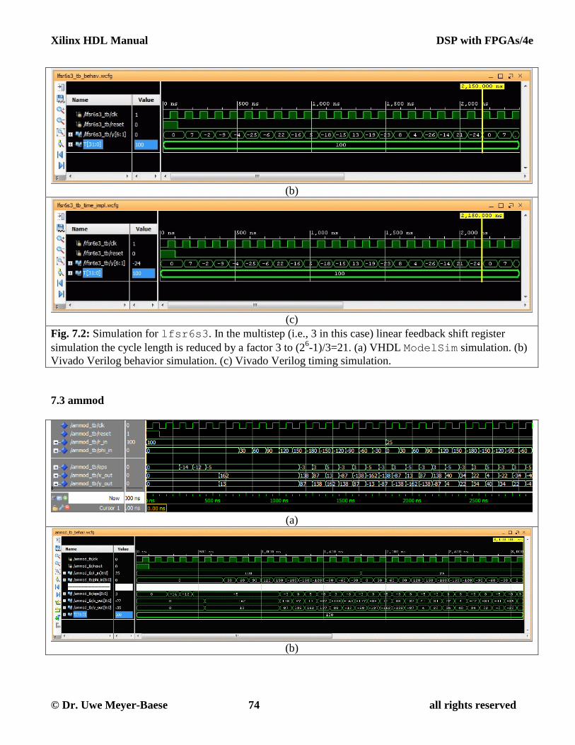
Fig. 7.2: Simulation for lfsr6s3. In the multistep (i.e., 3 in this case) linear feedback shift register
simulation the cycle length is reduced by a factor 3 to (26-1)/3=21. (a) VHDL ModelSim simulation. (b)
Vivado Verilog behavior simulation. (c) Vivado Verilog timing simulation.
7.3 ammod
(a)
(b)

Xilinx HDL Manual DSP with FPGAs/4e
© Dr. Uwe Meyer-Baese 75 all rights reserved
(c)
Fig. 7.3: Simulation for ammod. The amplitude modulation has been implemented with the CORDIC
algorithm. The simulation shows two amplitude values 100 and 25 and a linear increase by 30 degree
phase (phi) which gives a cycle length of 12 clock cycles. (a) VHDL ModelSim simulation. (b) Vivado
Verilog behavior simulation. (c) Vivado Verilog timing simulation.
Chapter 8
8.1 fir_lms
(a)

Xilinx HDL Manual DSP with FPGAs/4e
© Dr. Uwe Meyer-Baese 76 all rights reserved
(b)
(c)
Fig. 8.1: Simulation for fir_lms. This is a two tap adaptive filter design that “learns” the coefficients
f0= 43.3and f1=25. (a) VHDL ModelSim simulation. (b) Vivado Verilog behavior simulation. (c) Vivado
Verilog timing simulation.

Xilinx HDL Manual DSP with FPGAs/4e
© Dr. Uwe Meyer-Baese 77 all rights reserved
8.2 fir4dlms
(a)
(b)

Xilinx HDL Manual DSP with FPGAs/4e
© Dr. Uwe Meyer-Baese 78 all rights reserved
(c)
Fig. 8.2: Simulation for fir4dlms. This is a two tap pipelined delay adaptive filter design that “learns”
the coefficients f0= 43.3and f1=25 at a higher clock speed due to additional pipeline registers with the cost
of little more residual error. (a) VHDL ModelSim simulation. (b) Vivado Verilog behavior simulation.
(c) Vivado Verilog timing simulation.
8.3 g711alaw
(a)

Xilinx HDL Manual DSP with FPGAs/4e
© Dr. Uwe Meyer-Baese 79 all rights reserved
(b)
(c)
Fig. 8.3: Simulation for g711alaw. The simulations shows the a-law encoding and decoding and the
associate errors for a power-of-two input positive input sequence and a few negative inputs too. (a) VHDL
ModelSim simulation. (b) Vivado Verilog behavior simulation. (c) Vivado Verilog timing simulation.

Xilinx HDL Manual DSP with FPGAs/4e
© Dr. Uwe Meyer-Baese 80 all rights reserved
8.4 adpcm
(a)
(b)

Xilinx HDL Manual DSP with FPGAs/4e
© Dr. Uwe Meyer-Baese 81 all rights reserved
(c)
Fig. 8.4: Simulation for adpcm. The ADPCM CODEC shows a compression to a 4 bit signal. The
simulation shows the encoder (y_out) and the decoder (p_out). A fast triangular ramp is followed by a
constant 1000 value to demonstrate the reduced quantization error with adaptation over time. (a) VHDL
ModelSim simulation. (b) Vivado Verilog behavior simulation. (c) Vivado Verilog timing simulation.

Xilinx HDL Manual DSP with FPGAs/4e
© Dr. Uwe Meyer-Baese 82 all rights reserved
8.5 pca
(a)

Xilinx HDL Manual DSP with FPGAs/4e
© Dr. Uwe Meyer-Baese 83 all rights reserved
(b)

Xilinx HDL Manual DSP with FPGAs/4e
© Dr. Uwe Meyer-Baese 84 all rights reserved
(c)
Fig. 8.5.1: Simulation for pca. The overall learning behavior of the principle component analysis (PCA)
is shown. The first PC is learned when mu1 is active. The second PC is learned during the time mu2 is
active. (a) VHDL ModelSim simulation. (b) Vivado Verilog behavior simulation. (c) Vivado Verilog
timing simulation. The Verilog timing simulation does not match the behavior during the learning of the
second PC.

Xilinx HDL Manual DSP with FPGAs/4e
© Dr. Uwe Meyer-Baese 85 all rights reserved
(a)

Xilinx HDL Manual DSP with FPGAs/4e
© Dr. Uwe Meyer-Baese 86 all rights reserved

Xilinx HDL Manual DSP with FPGAs/4e
© Dr. Uwe Meyer-Baese 87 all rights reserved
(b)
(c)
Fig. 8.5.2: Simulation for pca. Values after convergence. The 2 system outputs “y” should give a good
approximations to the 2 input signals “s”. (a) VHDL ModelSim simulation. (b) Vivado Verilog behavior
simulation. (c) Vivado Verilog timing simulation. The simulation in (a,b) shows convergence in both
signals, however, simulation (c) does not converge for the second PC.

Xilinx HDL Manual DSP with FPGAs/4e
© Dr. Uwe Meyer-Baese 88 all rights reserved
8.6 ica
(a)

Xilinx HDL Manual DSP with FPGAs/4e
© Dr. Uwe Meyer-Baese 89 all rights reserved
(b)

Xilinx HDL Manual DSP with FPGAs/4e
© Dr. Uwe Meyer-Baese 90 all rights reserved
(c)
Fig. 8.6: Simulation for ica. The ICA system learns faster and is more robust than the PCA system.
Already after 20 µs the 2 output signals y1 and y2 are good approximations to the input signals s1 and
s2. (a) VHDL ModelSim simulation. (b) Vivado Verilog behavior simulation. (c) Vivado Verilog timing
simulation.

Xilinx HDL Manual DSP with FPGAs/4e
© Dr. Uwe Meyer-Baese 91 all rights reserved
Chapter 9
9.1 reg_file
(a)
(b)

Xilinx HDL Manual DSP with FPGAs/4e
© Dr. Uwe Meyer-Baese 92 all rights reserved
(c)
Fig. 9.1: Simulation for reg_file. First a normal write operations is shown. Register 0 is always 0.
Registers 1,2, and 3 store the values 2, 4, and 6, respectively. Then with reg_ena low registers 1 and 2
do not change values. (a) VHDL ModelSim simulation. (b) Vivado Verilog behavior simulation. (c)
Vivado Verilog timing simulation. The local variable “r” is not available in the timing simulation.
9.2 trisc0
(a)

Xilinx HDL Manual DSP with FPGAs/4e
© Dr. Uwe Meyer-Baese 93 all rights reserved
(b)
(c)
Fig. 9.2: Simulation for trisc0. The trisc0 is a stack machine that comes with a basic C-compiler
and assembler program. The simulation shows the computation of a factorial for 3, i.e. 2*3=6 done in a
loop. I/O ports are used to specify the factorial argument (iport) and the LEDs (oport) are used to
display the result. (a) VHDL ModelSim simulation. (b) Vivado Verilog behavior simulation. (c) Vivado
Verilog timing simulation.

Xilinx HDL Manual DSP with FPGAs/4e
© Dr. Uwe Meyer-Baese 94 all rights reserved
LICENSE AGREEMENT AND LIMITED WARRANTY
This manual contains scripts, programs, and HDL source code (hereinafter the "SOFTWARE") written by
Dr. Uwe Meyer-Baese and copyrighted by the author. Your payment of the license fee, which is part of
the price you paid for this product, grants you the nonexclusive right to use the enclosed SOFTWARE on
a single computer as long as you comply with the terms of this agreement. By agreeing to these terms, you
agree:
1. not to reproduce and/or sell the SOFTWARE for profit,
2. not to make more than a single copy of the SOFTWARE for backup,
3. not to display the SOFTWARE on the World Wide Web,
4. not to modify, adapt, or translate the SOFTWARE in order to create derivative commercial
products based on the SOFTWARE without prior written consent of the author.
If you do not agree with these terms and conditions, do not use the SOFTWARE. Non-commercial use of
the SOFTWARE is free. You are welcome to use the source code for research or teaching purposes, but
you must then include this Agreement with the code. If you modify the code for your own research, please
acknowledge the author as the source of the original code as follows:
-- Original source Copyright
-- Author of original HDL code: Dr. Uwe Meyer-Baese
-- Modified by: your name here
If your use of this SOFTWARE leads to publication, the author would appreciate a short (bibliographic) e-
mail at [email protected].
NO WARRANTY
THE ENCLOSED SOFTWARE IS DISTRIBUTED ON AN "AS IS" BASIS, WITHOUT WARRANTY.
NEITHER THE AUTHOR, THE SOFTWARE DEVELOPERS, NOR THE PUBLISHER MAKE ANY
REPRESENTATION OR WARRANTY, EITHER EXPRESSED OR IMPLIED, WITH RESPECT TO
THE SOFTWARE, ITS QUALITY, ACCURACY, OR FITNESS FOR A SPECIFIC PURPOSE. IN NO
EVENT, UNLESS REQUIRED BY APPLICABLE LAW OR AGREED TO IN WRITING, WILL ANY
COPYRIGHT HOLDER, OR ANY OTHER PARTY WHO MAY MODIFY AND/OR REDISTRIBUTE
THE PROGRAM AS PERMITTED ABOVE, BE LIABLE FOR DAMAGES, INCLUDING ANY
GENERAL, SPECIAL, INCIDENTAL OR CONSEQUENTIAL DAMAGES ARISING OUT OF THE
USE OR INABILITY TO USE THE PROGRAM (INCLUDING BUT NOT LIMITED TO LOSS OF
DATA OR DATA BEING RENDERED INACCURATE OR LOSSES SUSTAINED BY YOU OR
THIRD PARTIES OR A FAILURE OF THE PROGRAM TO OPERATE WITH ANY OTHER
PROGRAMS), EVEN IF SUCH HOLDER OR OTHER PARTY HAS BEEN ADVISED OF THE
POSSIBILITY OF SUCH DAMAGES.
END OF LICENSE AGREEMENT AND LIMITED WARRANTY
Xilinx HDL Manual DSP with FPGAs/4e
© Dr. Uwe Meyer-Baese 95 all rights reserved
What other professionals in this field say about DSP with FPGAs:
“Let me compliment you on the fine effort to produce this book.”
--Dr. Gerard Coutu, Instructor at Irvine who uses the book in class
“From the little I was able to read in a few hours I've realized the depth of your FPGA understanding.
Amazing. It's an honor to have people like you working at FSU.”
--Dan Belc, Development Engineer, Global Technology Development Group
(GTDG/R&D), MOTOROLA
“I've also lent your book to one of my DSP Application Engineers and she finds it great and very useful.”
--Tawfiq Mossadak, Altera University Program Manager
“ Very highly recommended by an expert in the field, January 30, 2002”
--Ray Andraka, P.E., President, Andraka Consulting Group, Inc.
--Book review at www.amazon.com
“I received your text today. It looks fantastic. Job well done..”
--Professor P. Athanas, Director Configurable Computing Lab, Virginia Tech.Uni.
“... a fundamental tool for anyone searching for the basics of advanced DSP with programmable logic. It
was difficult to improve the first edition, but the second one has done it…”
--Professor Dr. Antonio García, Uni. of Granada, Spain
Also available:
Floating-point design support
CSD, RAG, MAG, DA filter design HDL generator
HDL Code generation for DCT, DFT, FFT, CORDIC
Coming soon:
DSP with FPGAs: Verilog HDL Solution Manual
DSP with FPGAs: MatLab/Simulink HDL Lab Manual
DSP with FPGAs: Altera Simulink DSP Builder Lab Manual
DSP with FPGAs: Xilinx Simulink System Generator Lab Manual
ISBN: 0-9755494-6-4