Solid State Device Fundamentals - City University of … - Lectures... · Working temperature range...
23
Solid State Device Fundamentals ENS 345 Lecture Course by Alexander M. Zaitsev [email protected] Tel: 718 982 2812 4N101b College of Staten Island / CUNY Department of Engineering Science and Physics Solid State Device Fundamentals 4. Doped Semiconductors
Transcript of Solid State Device Fundamentals - City University of … - Lectures... · Working temperature range...
Solid State Device Fundamentals
ENS 345
Lecture Course
by
Alexander M. Zaitsev
[email protected]: 718 982 2812
4N101b
College of Staten Island / CUNY Department of Engineering Science and Physics
Solid State Device Fundamentals 4. Doped Semiconductors
Department of Engineering Science and Physics
Solid State Device Fundamentals
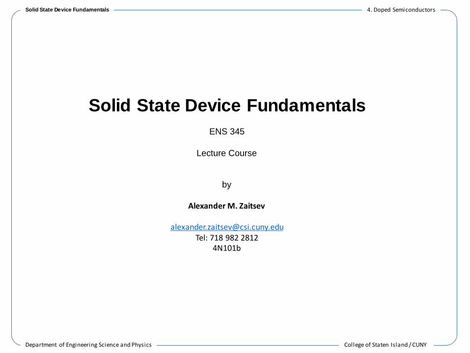
Doping semiconductors
Doped semiconductors are semiconductors, which contain impurities, foreign atomsincorporated into the crystal structure of the semiconductor. Either these impurities canbe unintentional, due to lack of control during the growth of the semiconductor, or theycan be added on purpose to provide free carriers in the semiconductor.
Ionization of a shallow donor and a shallow acceptor.
College of Staten Island / CUNY Department of Engineering Science and Physics
Solid State Device Fundamentals 4. Doped Semiconductors
2

College of Staten Island / CUNY Department of Engineering Science and Physics
Solid State Device Fundamentals 4. Doped Semiconductors
Dopants for doping A4 semiconductors
Solid State Device Fundamentals
Acceptors DonorsDopants in silicon and germanium
3

College of Staten Island / CUNY Department of Engineering Science and Physics
Solid State Device Fundamentals 4. Doped Semiconductors
Dopants for A3B5 semiconductors
Solid State Device Fundamentals
Dopants in GaAs
Acceptors Donors
As AsGa
Ga GaAs
AsGa Ga
n-type: tellurium, sulphur (substituting
As), tin, silicon, germanium (substituting
Ga).
p-type: zinc, chromium (substituting
Ga), silicon, germanium (substituting
As).4

College of Staten Island / CUNY Department of Engineering Science and Physics
Solid State Device Fundamentals 4. Doped Semiconductors
Ionization energy of dopants in semiconductors
Ionization energy of shallow donors and acceptors can be evaluated using hydrogenic model:
5
Trajectory of an electron bound to a
donor ion within a semiconductor crystal.
𝑟𝐷,𝐴 =4𝜋𝜀𝜀0ℏ
2
𝑚∗𝑒2~𝟏 𝒏𝒎
EHion
m0 e4
13.6 eV==8e0
2h2
Ionization energy EHion and orbital radius a0 of hydrogen atom
Ionization energy Eion and orbital radius 𝒓𝑫,𝑨 of donors and acceptors
Eion
m* e4
=8e2e0
2h2
~𝟓𝟎 𝒎𝒆𝑽

Energy levels of donors and acceptors
Conduction Band Ec
EvValence Band
Donor Level
Acceptor Level
Ed
Ea
Donor ionization energy
Acceptor ionization energy
Ionization energy of selected donors and acceptors in silicon
Acceptors
Dopant Sb P As B Al In
Ionization energy, E c–E d or E a–E v (meV) 39 44 54 45 57 160
Donors
College of Staten Island / CUNY Department of Engineering Science and Physics
Solid State Device Fundamentals 4. Doped Semiconductors
6

7
Dielectric constant of silicon is e = 11.7.Dielectric constant of germanium is e = 16.2.mn*/m0 = 0.26mp*/m0 = 0.39
Calculate the ionization energies and radii of donors and acceptors in Si and Ge.
Homework
Hydrogenic model of donors and acceptors
College of Staten Island / CUNY Department of Engineering Science and Physics
Solid State Device Fundamentals 4. Doped Semiconductors

2
innp =
Charge neutrality
2/1
2
2
22
= i
dada nNNNN
p
2/1
2
2
22
= i
adad nNNNN
n
College of Staten Island / CUNY Department of Engineering Science and Physics
Solid State Device Fundamentals 4. Doped Semiconductors
Since doped semiconductor, as a whole, is electroneutral, concentration of negative charges equals the concentration of positive charges.
DionizedAionized NpNn =
8

9College of Staten Island / CUNY Department of Engineering Science and Physics
Solid State Device Fundamentals 4. Doped Semiconductors
Homework
Concentration of electrons and holes
1. Calculate concentrations of electrons and holes in Si and Ge with donor concentration of 3x1017 cm-3 and acceptor concentration of 8x1016 cm-3 at room temperature.
2. Will these concentrations change much with temperature increase to 100°C?

Charge carrier concentration in doped semiconductor
College of Staten Island / CUNY Department of Engineering Science and Physics
Solid State Device Fundamentals 4. Doped Semiconductors
AD NNn =
nnp i
2=
iAD nNN
if , AD NN di Nnp
2=andn = ND
n-type
ida nNN da NNp =
pnn i
2=
if , da NN aNp =
ai Nnn2
=and
p-type
10

Dopant compensation: Example
What are n and p in Si with (a) ND = 61016 cm-3 and NA = 21016 cm-3 and (b) additional 61016 cm-3 of NA?
(a)
(b) Na = 21016 + 61016 = 81016 cm-3 > Nd
316cm104 == ad NNn
3316202cm105.2104/10/ === nnp i
3161616 cm102106108 === da NNp
3316202cm105102/10/ === pnn i
+ + + + + + . . . . . .
. . . . . . . . . . .
Nd = 61016 cm-3
Na = 21016 cm-3
n = 41016 cm-3
+ + + + + +
- - - - - - - -
. . . . . .
. . . . . .
Nd = 61016 cm-3
Na = 81016 cm-3
p = 21016 cm-3
College of Staten Island / CUNY Department of Engineering Science and Physics
Solid State Device Fundamentals 4. Doped Semiconductors
The resulting carrier density in compensated material
is approximately equal to the difference between the
donor and acceptor concentration:
11

12College of Staten Island / CUNY Department of Engineering Science and Physics
Solid State Device Fundamentals 4. Doped Semiconductors
Homework
Charge carrier concentration in n-type and p-type semiconductor
1. Calculate concentrations of electrons and holes in Si and Ge containing 3x1017 cm-3 donors and 8x1016 cm-3 acceptors at room temperature with assumption NA, ND >> ni.
2. Compare the obtained values with those calculated in Homework on slide 9.

Position of Fermi level versus dopant concentration
kTEE
CFCeNn
/)( =
nNkTEE CCF ln=
College of Staten Island / CUNY Department of Engineering Science and Physics
Solid State Device Fundamentals 4. Doped Semiconductors
kTEE
VVFeNp
/)( =
pNkTEE VVF ln=
With concentration of donors, the Fermi level approaches the conduction band.With concentration of acceptors, the Fermi level approaches the valence band.
13
Fermi energy of doped silicon (n-type and p-type) vary with doping density. As the doping increases, Fermi level shifts towards conduction band (Ec) in the case of n-type doping and shifts towards valance band (Ev) in p-type doping. Note where Fermi level crosses Conduction (valance) band).

The Fermi level and carrier concentration
College of Staten Island / CUNY Department of Engineering Science and Physics
Solid State Device Fundamentals 4. Doped Semiconductors
kTEE
CFCeNn
/)( =
eV 614.010/108.2ln026.0
ln
1719 ==
== nNkTEE CFC
Where is EF for n =1017 cm-3?ECEF
EC
0.146 eV
eV 31.010/1004.1ln026.0
ln
1419 ==
== pNkTEE VVF
Where is EF for p = 1014 cm-3 ?
kTEE
VVFeNp
/)( =
0.31 eV
EC
EF
EV
14

15College of Staten Island / CUNY Department of Engineering Science and Physics
Solid State Device Fundamentals 4. Doped Semiconductors
Homework
Position of Fermi level in n-type and p-type semiconductor
1. Calculate position of Fermi level in n-type silicon with donor concentration of 3x1017 cm-3 at room temperature.
2. Calculate position of Fermi level in p-type silicon with acceptor concentration of 8x1016 cm-3 at room temperature.

College of Staten Island / CUNY Department of Engineering Science and Physics
Solid State Device Fundamentals 4. Doped Semiconductors
As the temperature increases Fermi level shifts towards the middle of the bandgap.
Position of Fermi level in doped semiconductor versus temperature
16
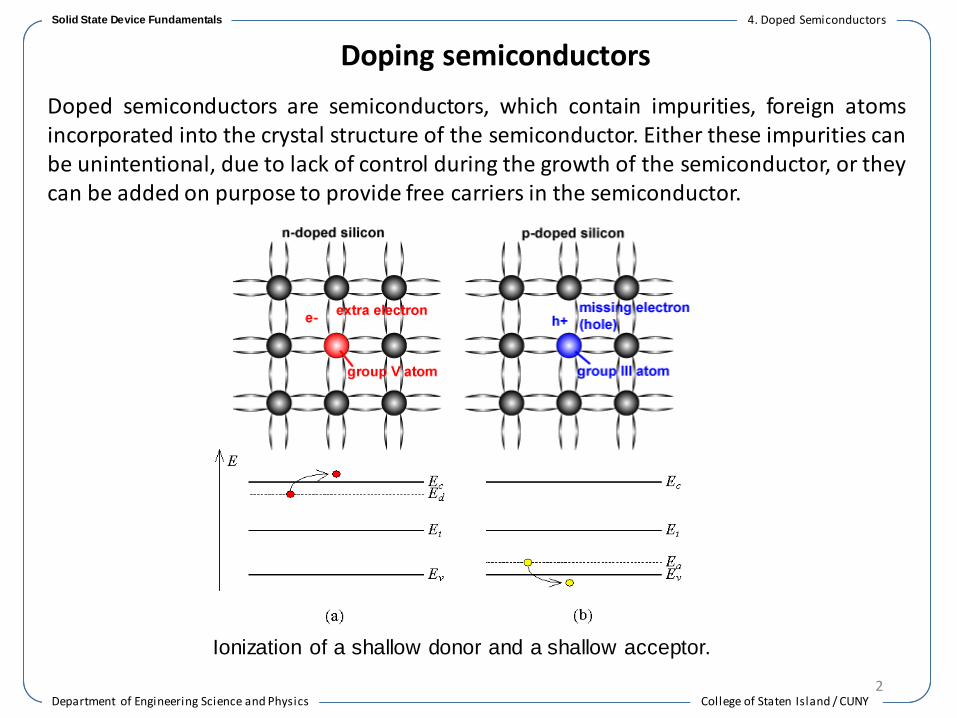
ND = 1017 cm-3. What fraction of the donors are not ionized?
Solution: First assume that all the donors are ionized.
Probability of not being ionized:
04.05.01
1
5.01
1meV26/)meV)45146((/)(
=
=
eekTEE FD
It is reasonable to assume that at room temperature the complete ionization occur, i.e., n = ND .
Is assumption n = ND valid for low doped semiconductors?
meV146cm10 317 ===
CFD EENn Ec
Ef
Ev
146 meV
Ed
45meV
Complete ionization of dopants
College of Staten Island / CUNY Department of Engineering Science and Physics
Solid State Device Fundamentals 4. Doped Semiconductors
17

Example: Carrier concentrations
What is the hole concentration in an n-type semiconductor with 1015 cm-3 of donors?
n = 1015 cm-3.
After increasing temperature by 60C, n remains the same at 1015 cm-3
while p increases by about a factor of 2300 because of thermal activation..
What is n if p = 1017cm-3 in a p-type silicon wafer?
3-5
315
-3202
cm10cm10
cm10==
n
np i
kTE
igen
2/2
3-3
317
-3202
cm10cm10
cm10==
p
nn i
College of Staten Island / CUNY Department of Engineering Science and Physics
Solid State Device Fundamentals 4. Doped Semiconductors
18

19College of Staten Island / CUNY Department of Engineering Science and Physics
Solid State Device Fundamentals 4. Doped Semiconductors
Homework
Position of Fermi level in n-type and p-type semiconductor at elevated temperature
1. Calculate position of Fermi level in n-type silicon with donor concentration of 3x1017 cm-3 at a temperature of 200°C.
2. Calculate position of Fermi level in p-type silicon with acceptor concentration of 8x1016 cm-3 at a temperature of 200°C.

Temperature dependence of charge carrier concentration
kTEEDC DCeNN
n2/)(
2/1
2
=Low T:
College of Staten Island / CUNY Department of Engineering Science and Physics
Solid State Device Fundamentals 4. Doped Semiconductors
Electron density as a function of temperature in silicon with:ND = 1016 cm-3
NA = 1014 cm-3
EC - ED = EA - EV = 50 meV.
RT300°CLNT
n = Nd
High T:kTE
VCigeNNnpn
2/===
20

Working temperature range of semiconductor device
College of Staten Island / CUNY Department of Engineering Science and Physics
Solid State Device Fundamentals 4. Doped Semiconductors
At high temperatures, the electrical difference between the n and p regions disappears and the p-n junction becomes ineffective in controlling carrier movement.
The basic upper temperature limit of semiconductor material is determined by its bandgap energy. A rule-of-thumb is that the maximum temperature (in K) is approximately 500 times the bandgap energy in eV. For Si this rule gives Tmax ~ 290°C.
The lower temperature limit is determined by the thermal ionization energy of the dopants. If the temperature is too low, the dopants are not sufficiently ionized and there are no insufficient charge carriers. The result is a condition called "freeze-out." For example, silicon freezes out at about 40 K.
21

Dependence of the temperature range on doping
College of Staten Island / CUNY Department of Engineering Science and Physics
Solid State Device Fundamentals 4. Doped Semiconductors
The higher dopant concentration the wider the temperature range
22

23College of Staten Island / CUNY Department of Engineering Science and Physics
Solid State Device Fundamentals 4. Doped Semiconductors
Homework
Working temperature range
1. High Temperature Limit: For n-type silicon with 1016 cm-3 phosphorous donors, at what temperature the concentration of holes is 10% of that of electrons?
2. Low Temperature Limit: For n-type silicon with 1016 cm-3 phosphorous donors, at what temperature the concentration of electrons is 10% of that of donors?