Solid State Detectors- 6 T. Bowcock 2 Schedule 1Position Sensors 2Principles of Operation of Solid...
44
Solid State Detectors- 6 T. Bowcock
-
date post
20-Dec-2015 -
Category
Documents
-
view
220 -
download
0
Transcript of Solid State Detectors- 6 T. Bowcock 2 Schedule 1Position Sensors 2Principles of Operation of Solid...

Solid State Detectors- 6
T. Bowcock

2
Schedule
1 Position Sensors
2 Principles of Operation of Solid State
Detectors
3 Techniques for High Performance Operation
4 Environmental Design
5 Measurement of time
6 New Detector Technologies

3
New Technologies
• Si developments– Oxygenated Si– p-type Si
• Diamond• Cryogenic Si• Deep Sub-Micron Processing• Nanotechnologies• Physics
4
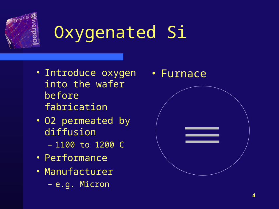
Oxygenated Si
• Introduce oxygen into the wafer before fabrication
• O2 permeated by diffusion– 1100 to 1200 C
• Performance• Manufacturer
– e.g. Micron
• Furnace

5
Oxygenated Si

6
Oxygenated Si
Trying to unfold the performance

7
Oxygenated Si
• Performance with diodes superb– factor 2
improvement
• Strip performance seems to be about 20% better
8
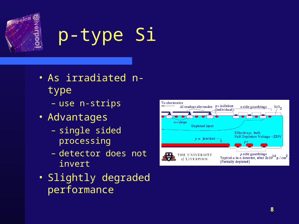
p-type Si
• As irradiated n-type– use n-strips
• Advantages– single sided
processing– detector does not
invert
• Slightly degraded performance

9
P-type Si
10
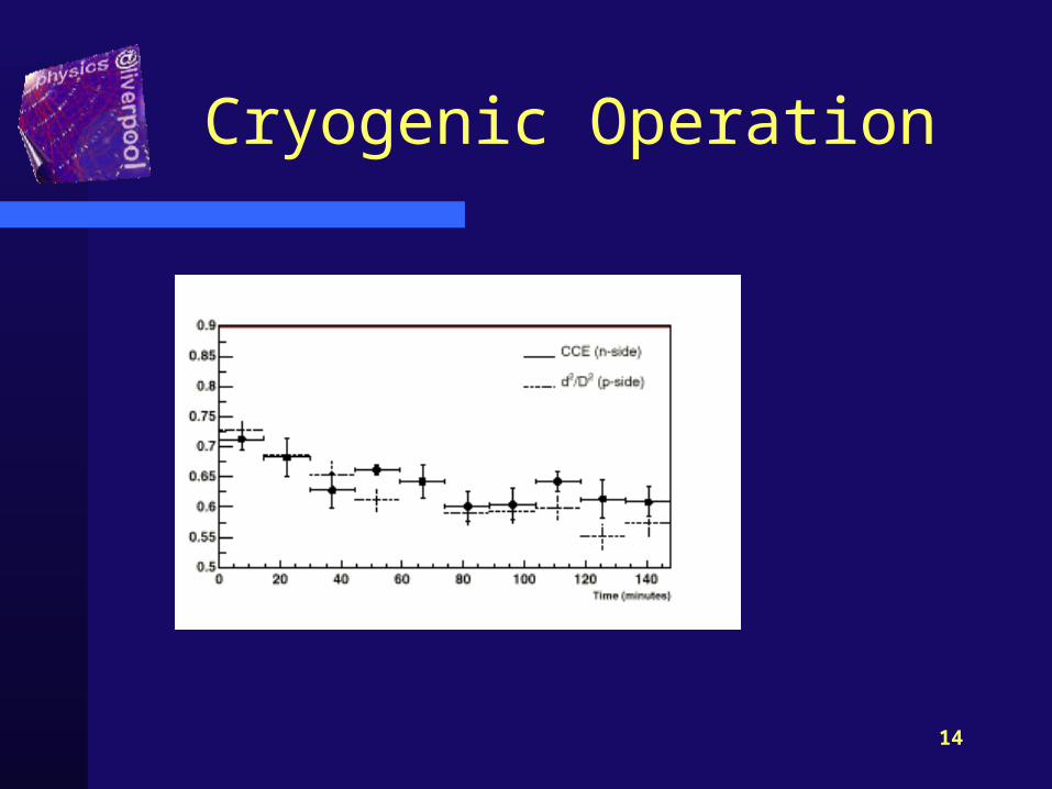
Cryogenic Operation
• Lazarus Effect– cool detector down it appears to repair itelf– standard technology but cold– diodes
• Strip detectors irradiated while cold– double sided– monitor both p and n side
11
Cryogenic Operation
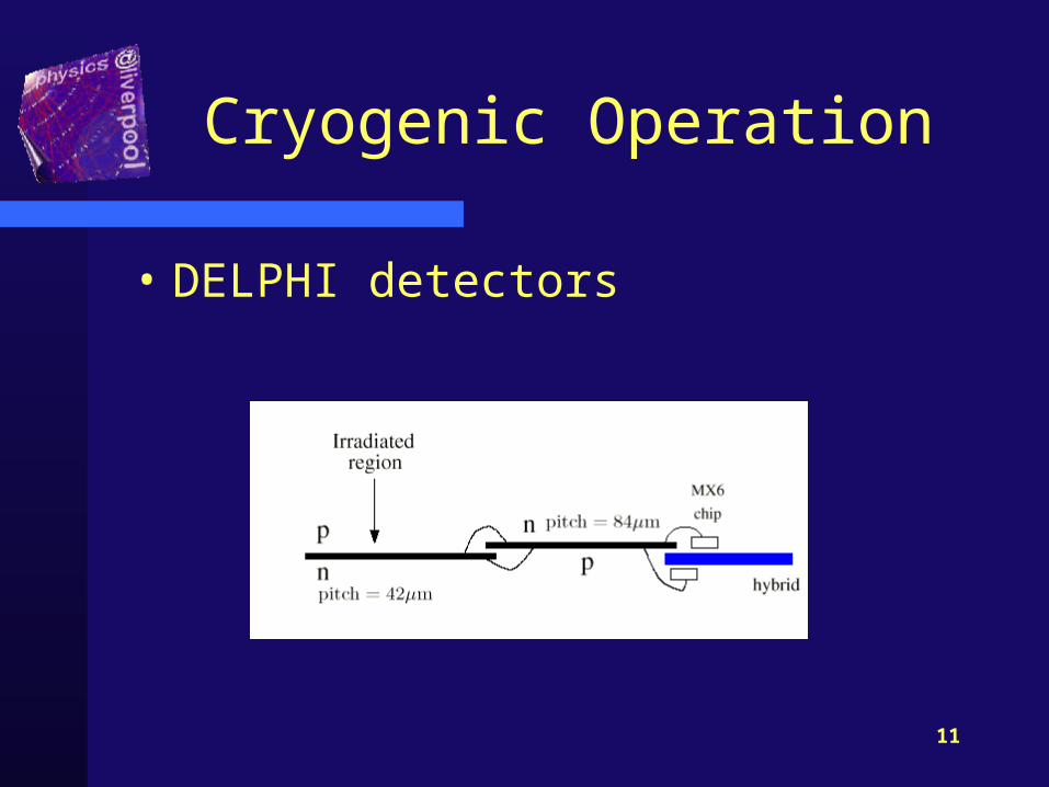
• DELPHI detectors

12
Cryogenic Operation

13
Cryogenic operation
14
Cryogenic Operation

15
Cryogenic Operation
• Lazarus effect could be observed– charge injection into a reverse biased
detector– filling traps with electrons– uncontrolled– fine tuned with temperature&frequency
• Is there a way to control this?

16
Diamond
• Use Diamond as a material– radiation hard– cheap(!)– large area

17
Diamond Formation
• Chemical Vapour Deposition(CVD)
substrate
Small crystals of order microns
Larger crystals 20-30 microns
18
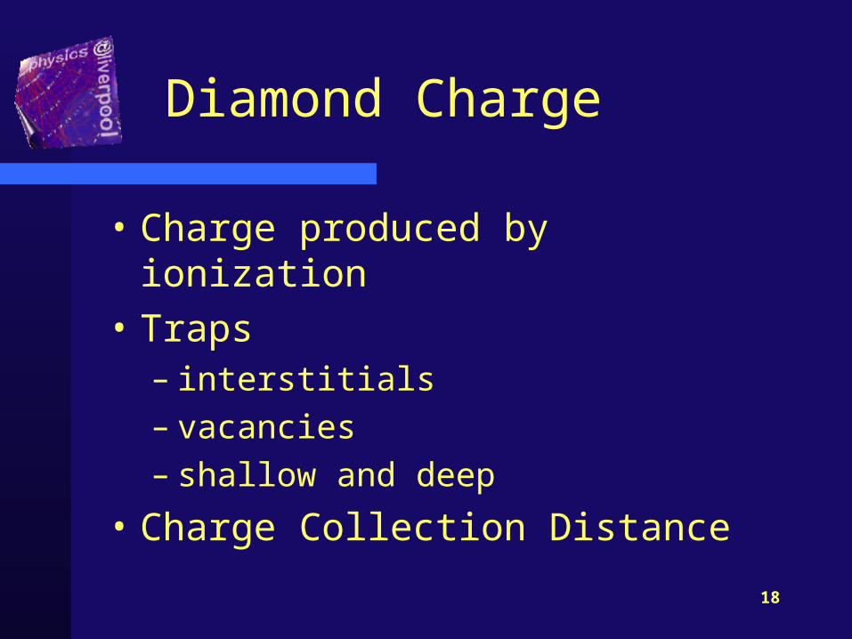
Diamond Charge
• Charge produced by ionization
• Traps– interstitials– vacancies– shallow and deep
• Charge Collection Distance

19
Diamond Performance
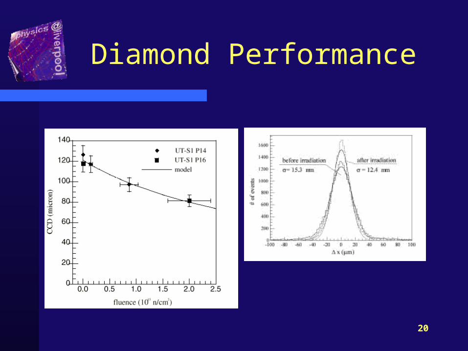
20
Diamond Performance

21
Diamond
• Very high fluences– at current radiation levels does not out
perform Si– limited charge collection distance
• small crystals?

22
Summary of Current New Technologies
• Si reaching maturity– extension such as O2 fine tune
performance
• New generation of materials (e.g. diamond) can be used under extreme conditions
23
Speculative Technology
• Plastic diodes
• New Si processing

24
Organic diodes
• “In 1989 it was discovered that a conjugated polymer, poly(1,4-phenylenevinlyene) (PPV), could be used as a light emitting layer in LEDs. This discovery has wide ranging commercial possibilities, e.g., the preparation of lightweight, large, multicoloured, flat panel displays for televisions and computer screens is now a realistic possibility”. (D. Burn).
PPV

25
Polymer Diodes
• A simple LED consists of a polymer sandwiched between two metal electrodes.
• The electrons and holes charges move in opposite directions and if they end up on the same polymer chain then they can form a singlet excited state which can decay and emit light
• The colour of the light is dependent on the HOMO-LUMO energy gap.

26
Polymer diodes
• TV screens– very commercial
• If becomes viable perhaps we can benefit
• R&D– flexible – robust– cheap
27
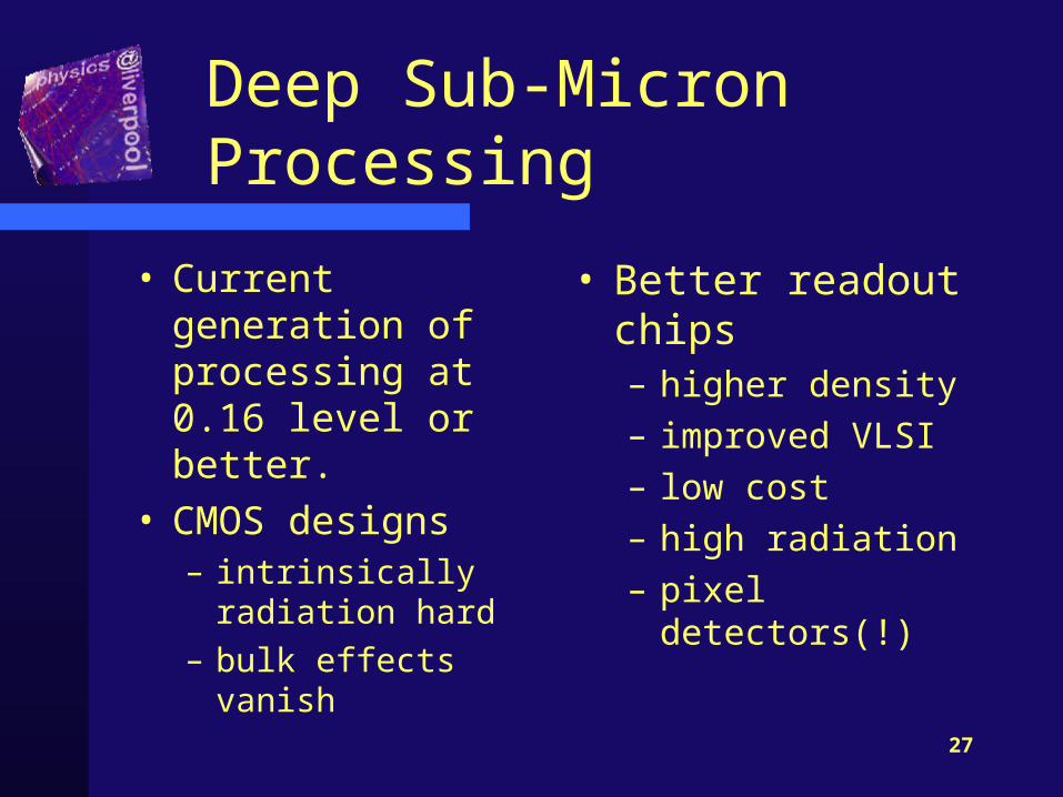
Deep Sub-Micron Processing
• Current generation of processing at 0.16 level or better.
• CMOS designs– intrinsically
radiation hard– bulk effects vanish
• Better readout chips– higher density– improved VLSI– low cost– high radiation– pixel detectors(!)

28
Deep Sub-Micron
• Large areas
• High resolution
• What we need for large area high quality production of detectors
• COST inhibitive at the moment– CCD large scale high resolution

29
Nanotechnology
• Look and manufacture things on the sub-nm scale
• Si(111) surface• GaAs

30
Nanotechnology
• A 200 Å x 200 Å constant current STM image of an alpha-Fe2O3(0001) surface . This image shows two types of island, which are ordered, forming a hexagonal superlattice. The unit cell of the superlattice has a characteristic dimension of 40 ± 5 Å and is rotated by 30 degrees from the alpha-Fe2O3(0001) lattice.

31
Nanotechnology
• If we could find a way of recording mip through a material– ultimate 0.1 nm scale detector– electronic (slow!) r/o

32
Physics
• From applied physics point of view all these technologies are very interesting
• How applicable are they to particle physics?• Ultimate measurement as resolution
improves

33
Particle Physics
• Detector resolution– Vertex
• topology of vertex • decay lengths
– Tracking • momentum of particles• usually large volume gas detector

34
Vertex Finding
• Heavy quarks decay quickly– b in about 1ps (mm in current machines)– t in fs or less (where primary
hadronisation occurs)
• Increasing resolution would improve our separation of b-quarks from the primary collision – decrease luminosity
35
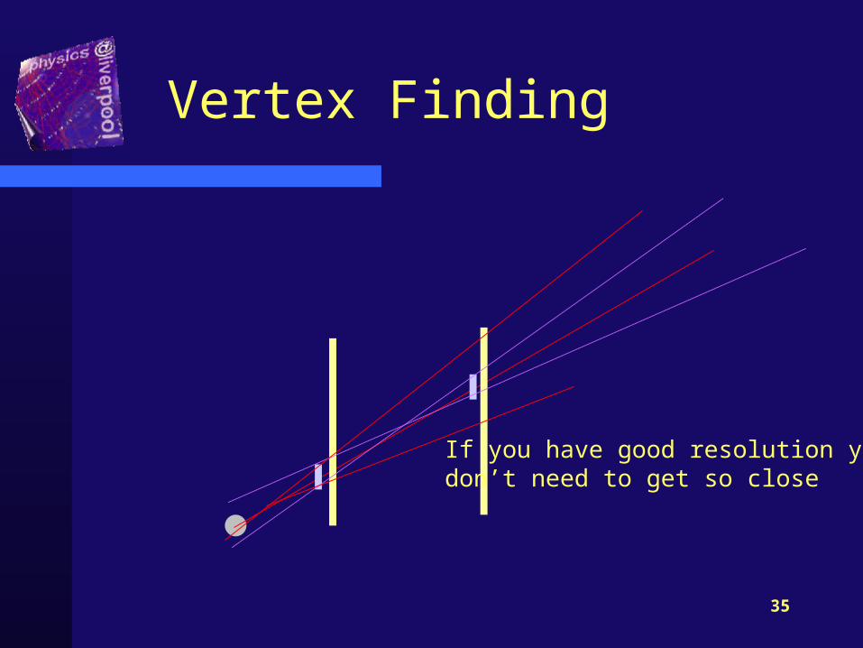
Vertex Finding
If you have good resolution you don’t need to get so close
36
Vertex Finding
• In telescope– limited by mechanical accuracy – thermal expansion etc
• Practical limit to resolution JUST from these considerations O(1 micron)
• Multiple Scattering
37
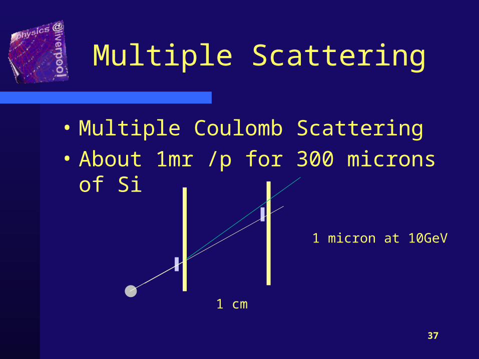
Multiple Scattering
• Multiple Coulomb Scattering
• About 1mr /p for 300 microns of Si
1 micron at 10GeV
1 cm
38
Multiple Scattering
• Angles give mass resolution for hadronic decays
• Already ms limited in many cases– slow pions < 0.5 GeV/c
• HEP seems to be less interested in hadronic decays masses than decay rates– CPT not approachable by this method
39
Vertex Finding
• For fast (active r/o) devices we are probably within a factor 10 of limit with current technology
• Topology of the decays– thin retaining signal– surface nano-readout– alignment?

40
Tracking
• High resolution detectors useful– detectors have large gas volumes– large volumes make calorimetry
expensive
• Momentum measurement
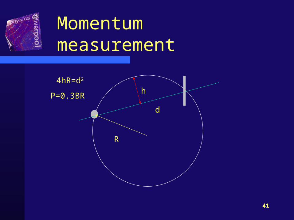
41
Momentum measurement
R
h
d
4hR=d2
P=0.3BR
42
Momentum Measurement
• Measurement of sagitta is key– multiple scattering counts– Si usually not used– Time Projection Chamber (?)

43
Summary (New Technology)
• We are close to performance limits (for what we need) … micron level precision active detectors
• New Technology gives performance in extreme cases– e.g. radiation– extreme resolution– cost
44
Conclusion
• Detectors have developed in 100yrs
• Understood basic solid state detectors
• Research that is being followed
• New Horizons/Technologyes
• Up to you to have the good ideas– and find the physics that needs it