
Large Size GEM Detectors for 12 GeV Program in Hall A at JLab
SoLID GEM Detectors in US
Kondo Gnanvo University of Virginia
SoLID Collaboration Meeting @ Jlab, 01/13/2016
Outline
Overview of SoLID GEM Trackers
Large area GEM R&D @ UVa
Update on APV25 Electronics
SoLID GEM-US Pre-R&D

SoLID Collaboration Meeting @ JLab
Overview of SoLID GEM Trackers
1/13/2016 2
6 disk layers
5 disk layers
PVDIS
SIDIS
Tracking requirements for PVDIS
Luminosity ~ 1039/cm2/s
Rate: from 100 kHz/cm2 to 600 kHz/cm2 (with
baffles) from GEANT4 estimation
Spatial Resolution: ~ 100 µm (σ) in azimuthal
direction
Total area: ~37 m2 total area (30 sectors × 5
planes, each sector covering 12 degree)
Need radiation and magnetic field tolerant
Idea
Use the same set of GEM modules for all 3 configurations (PVDIS, SIDIS and J/ψ)
All electronics channels from PVDIS would be more than enough for SIDIS and J/ψ

SoLID Collaboration Meeting @ JLab
Overview of SoLID GEM Trackers: Large area GEM challenges
1/13/2016 3
SoLID needs GEM modules as large as 113 cm × 44 cm for the larger disk of PVDIS
The biggest challenge used to be the non-availability of large area GEM foils.
Previously limited by double mask technique for etching: hard to the two masks accurately:
Max area was limited to ~ 45 cm × 45 cm
New Single Mask technique allows to make GEM foils as large as 200 cm × 55 cm
The remaining challenge is large production capacity:
If all LHC related large GEM project (CMS, ALICE, TOTEM) gets underway, this will
require almost 100 % of CERN production capacity
Currently work going on for large GEM production capabilities in China and in the US.

Characterization with Cosmics
PRad: Proton Radius Experiment in Hall A @ JLab (E12-11-106)
SoLID Collaboration Meeting @ JLab
Large Area GEM R&D @ UVa: The PRad GEM Trackers
1/13/2016 4
Characteristics of PRad GEM trackers
2 large triple-GEM chambers (~ 122 cm × 55 cm)
Largest GEM ever built, bigger than the largest SoLID GEM module
COMPASS style 2D Cartesian strip readout : long narrow strip (> 130
cm) → but still low capacitance noise
PRad triple-GEM detector
(active area: 122 cm × 55 cm)
SoLID Collaboration Meeting @ JLab
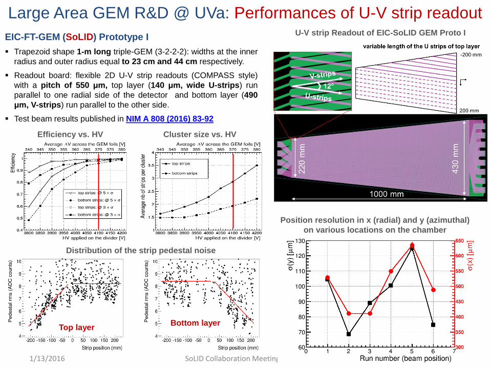
Large Area GEM R&D @ UVa: Performances of U-V strip readout
1/13/2016 5
EIC-FT-GEM (SoLID) Prototype I
Trapezoid shape 1-m long triple-GEM (3-2-2-2): widths at the inner
radius and outer radius equal to 23 cm and 44 cm respectively.
Readout board: flexible 2D U-V strip readouts (COMPASS style)
with a pitch of 550 μm, top layer (140 μm, wide U-strips) run
parallel to one radial side of the detector and bottom layer (490
μm, V-strips) run parallel to the other side.
Test beam results published in NIM A 808 (2016) 83-92
Efficiency vs. HV Cluster size vs. HV
Top layerBottom layer
Distribution of the strip pedestal noise
Position resolution in x (radial) and y (azimuthal)
on various locations on the chamber
U-V strip Readout of EIC-SoLID GEM Proto I

SoLID Collaboration Meeting @ JLab
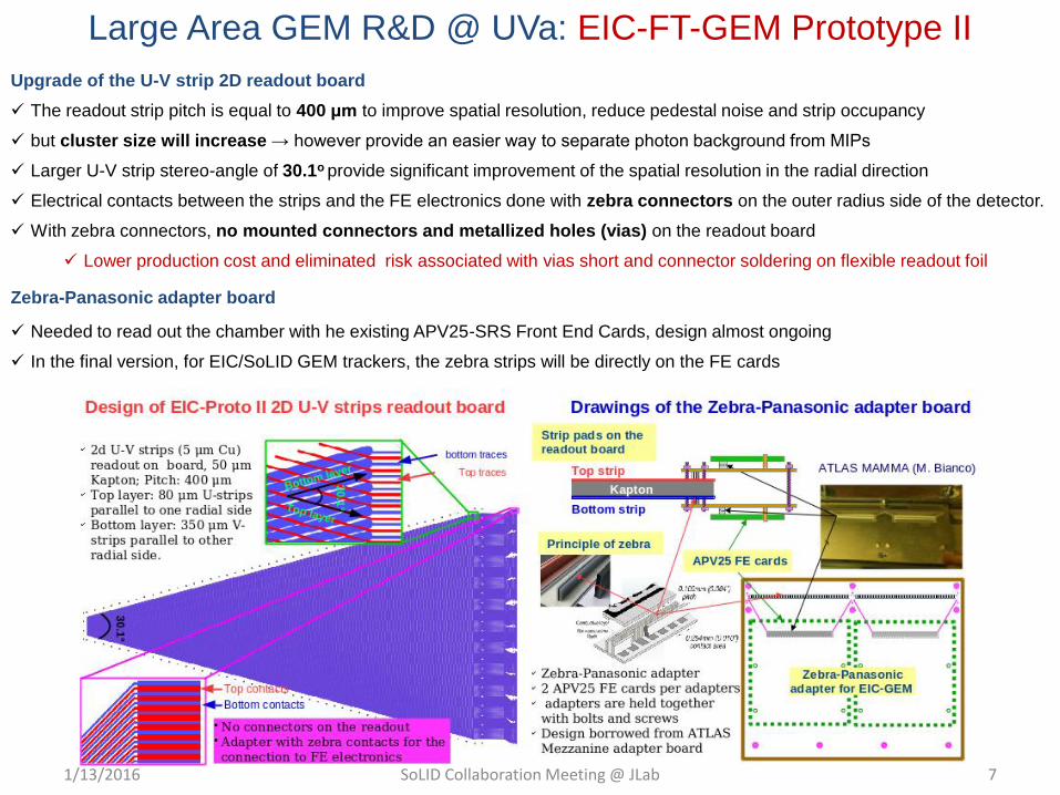
Large Area GEM R&D @ UVa: EIC-FT-GEM Prototype II
1/13/2016 6
Common GEM foil for EIC Forward Tracker R&D:
Common GEM foil design developed by three groups at UVa,
Florida Tech (M. Hohlmann), and Temple University (B. Surrow).
Active area: A trapezoid foil with a length of 903.57 mm, widths at
both ends equal to 43 mm and 529 mm and an opening angle of
30.1o.
Opening angle of the trapezoid is 30.1 deg., allows some overlap
when making a disk from 12 detectors.
All HV sectors connections and gas flow structure are made on
the large radius end.
Honeycomb support are removed for a low mass detector
Share a lot of features with SoLID Trackers GEMs
Common GEM foil for EIC-FT-GEM proto II
(design by A. Zhang @ Florida Tech)
Novel assembly method for light weight GEM for EIC/SoLID New assembly method:
Ongoing work on the design of proto II of
Forward Tracker Detector R&D of EIC
Similar assembly technique for the pRad GEM
chambers
Foils are glued to frames but frames not glued
together but sealed with O-rings and bolts
could be re-opened.
SoLID Collaboration Meeting @ JLab1/13/2016 7
Upgrade of the U-V strip 2D readout board
The readout strip pitch is equal to 400 μm to improve spatial resolution, reduce pedestal noise and strip occupancy
but cluster size will increase → however provide an easier way to separate photon background from MIPs
Larger U-V strip stereo-angle of 30.1o provide significant improvement of the spatial resolution in the radial direction
Electrical contacts between the strips and the FE electronics done with zebra connectors on the outer radius side of the detector.
With zebra connectors, no mounted connectors and metallized holes (vias) on the readout board
Lower production cost and eliminated risk associated with vias short and connector soldering on flexible readout foil
Zebra-Panasonic adapter board
Needed to read out the chamber with he existing APV25-SRS Front End Cards, design almost ongoing
In the final version, for EIC/SoLID GEM trackers, the zebra strips will be directly on the FE cards
Large Area GEM R&D @ UVa: EIC-FT-GEM Prototype II

SoLID Collaboration Meeting @ JLab
Low-Mass GEM R&D: Chromium GEM foil (Cr-GEM)
1/13/2016 8
Standard GEM
5 m Cu
50 m Kapton
100 nm Cr50 m Kapton
Cr-GEM
100 nm Cr
Cr-GEM foil:
Copper (Cu) clad raw material comes with 100
nm Chromium (Cr) layer between Cu and Kapton,
5m Cu layers removed, leave only 100 nm
residual Cr layers as electrodes, Cr-GEM foils
provided CERN PCB workshop
Using Cr-GEM foil lead to almost 50% reduction
of the material of an SoLID-like light weight triple-
GEM detector: this is because the material in a
lightweight triple-GEM is dominated by the GEM
foils & readout board
SoLID Collaboration Meeting @ JLab
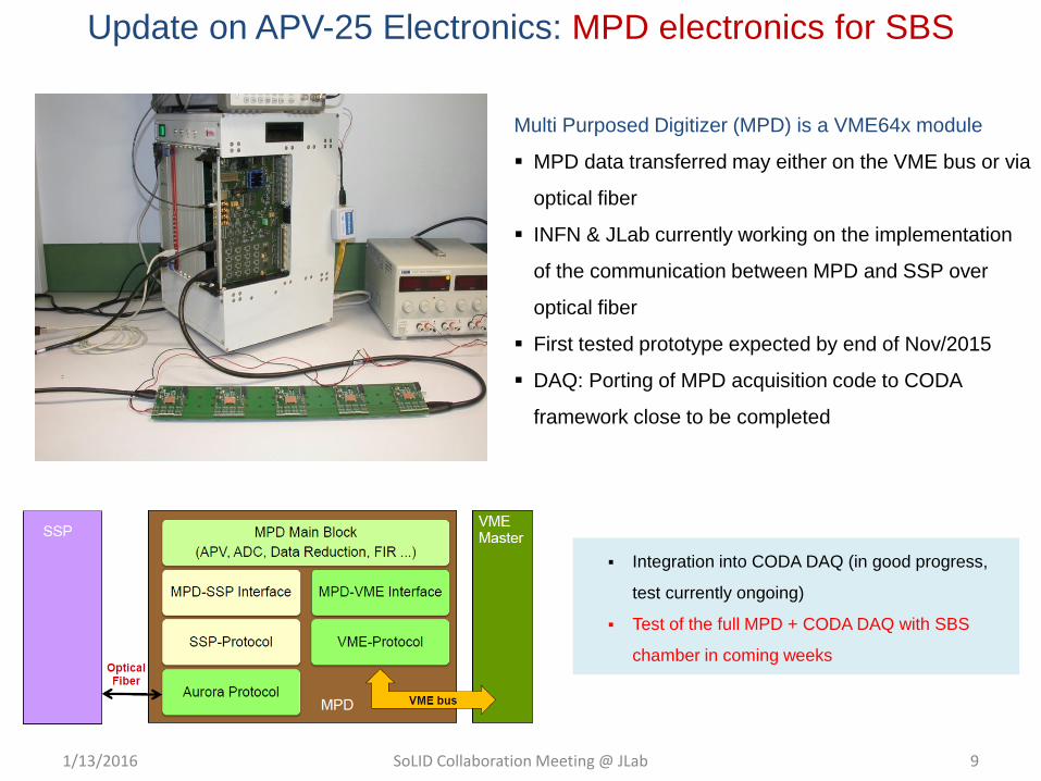
Update on APV-25 Electronics: MPD electronics for SBS
1/13/2016 9
Multi Purposed Digitizer (MPD) is a VME64x module
MPD data transferred may either on the VME bus or via
optical fiber
INFN & JLab currently working on the implementation
of the communication between MPD and SSP over
optical fiber
First tested prototype expected by end of Nov/2015
DAQ: Porting of MPD acquisition code to CODA
framework close to be completed
Integration into CODA DAQ (in good progress,
test currently ongoing)
Test of the full MPD + CODA DAQ with SBS
chamber in coming weeks

SoLID Collaboration Meeting @ JLab
Update on APV-25 Electronics: SRS electronics for PRad
1/13/2016 10
The Scalable Readout System (SRS)
APV25-based system developed by the international RD51 Coll. based @ CERN
Front End cards on the chamber host the APV25 chip ➩ data to ADC via HDMI cables
ADC cards interfaced with the FPGA board (FEC card) ➩ FEC data fragment to the SRU
SRU send the data fragment from many FECs to the DAQ PC through Gb Ethernet
The Need for PRad GEMs readout:
Peak trigger rate 5 kHz
72 APV25-FE cards (9216 channels), 6 (8*) ADC/FECs ⇨ 2 SRU boards
Implementation of the 10 Gb Optical link for the SRU (done)
Integration of SRS into CODA DAQ (in good progress, test currently ongoing)
SoLID Collaboration Meeting @ JLab
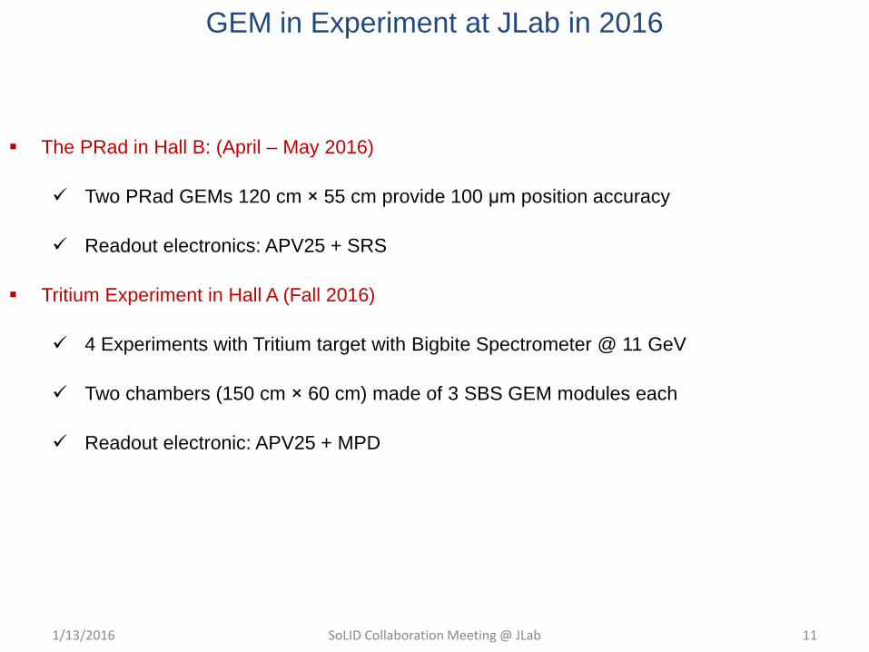
GEM in Experiment at JLab in 2016
1/13/2016 11
The PRad in Hall B: (April – May 2016)
Two PRad GEMs 120 cm × 55 cm provide 100 μm position accuracy
Readout electronics: APV25 + SRS
Tritium Experiment in Hall A (Fall 2016)
4 Experiments with Tritium target with Bigbite Spectrometer @ 11 GeV
Two chambers (150 cm × 60 cm) made of 3 SBS GEM modules each
Readout electronic: APV25 + MPD

SoLID Collaboration Meeting @ JLab
SoLID GEM-US Pre-R&D program: Plan for the next 2 years
1/13/2016 12
First year 2016:
Study of the performance of GEM in high background rate environment
Data with x-ray source combine with cosmic (and/ or 90Sr) to provide the input on the GEM
efficiency in high rate environment needed for the evaluation of the tracking efficiency by the
tracking reconstruction software group
Optimization of the design of different GEM modules size needed to equipped all layers in all
PVDIS / SIDIS / J/ψ configuration
Acquire a few Chinese GEM foils for test and characterization
Electrical test, Performance comparison with standard CERN foils
Readout electronics for SoLID GEMs
Identify the need for SoLID GEM tracking and specification for the ideal chip
Survey of the candidate chips available on the market other than APV25, DREAM and VMM
Second year 2017:
SoLID GEM chambers design & prototyping
Assembly of a prototype for the most challenging geometry (can even use Chinese GEM foils)
Applied experience learned from the EIC-FT-GEM R&D prototype II
Readout electronics for SoLID GEMs
Acquire a few VMM electronics from RD51 for tests with the SRS DAQ

90Sr
SoLID Collaboration Meeting @ JLab
SoLID GEM-US Pre-R&D program: High rate studies for SBS
1/13/2016 13
X-ray box setup @ UVa:
Photon energy range: up to 50 keV
Angular distribution: uniform within 60o
Output flux: 24 MHz/cm2 on the surface of GEM for 20
keV/ and current 5 μA
Charge deposition in GEM:
Conversion rate about 0.5% to electrons for ionization
up to 3.4*1011 electrons/cm2/s equivalent to about 7 MHz
/ cm2 MIP.

SoLID Collaboration Meeting @ JLab
SoLID GEM-US Pre-R&D program: High rate studies for SBS
1/13/2016 14
No cut
Cut on
position
Cut on
APV timing
correlation
Cut on
large ADC
value
Hit map Cluster size
APV timing
x vs. y
correlationADC x vs. y
correlation
ADC x/y
ratio
Cluster
multiplicity
These data produced for this study could be used as input for the tracking efficiency for SoLID
SoLID Collaboration Meeting @ JLab
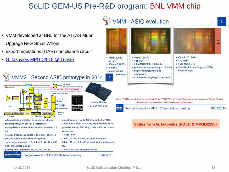
SoLID GEM-US Pre-R&D program: BNL VMM chip
1/13/2016 15
Slides from G. Iakovidis (RD51/ & MPGD2105)
VMM developed at BNL for the ATLAS Muon
Upgrage New Small Wheel
export regulations (ITAR) compliance circuit
G. Iakovidis MPGD2015 @ Trieste
SoLID Collaboration Meeting @ JLab
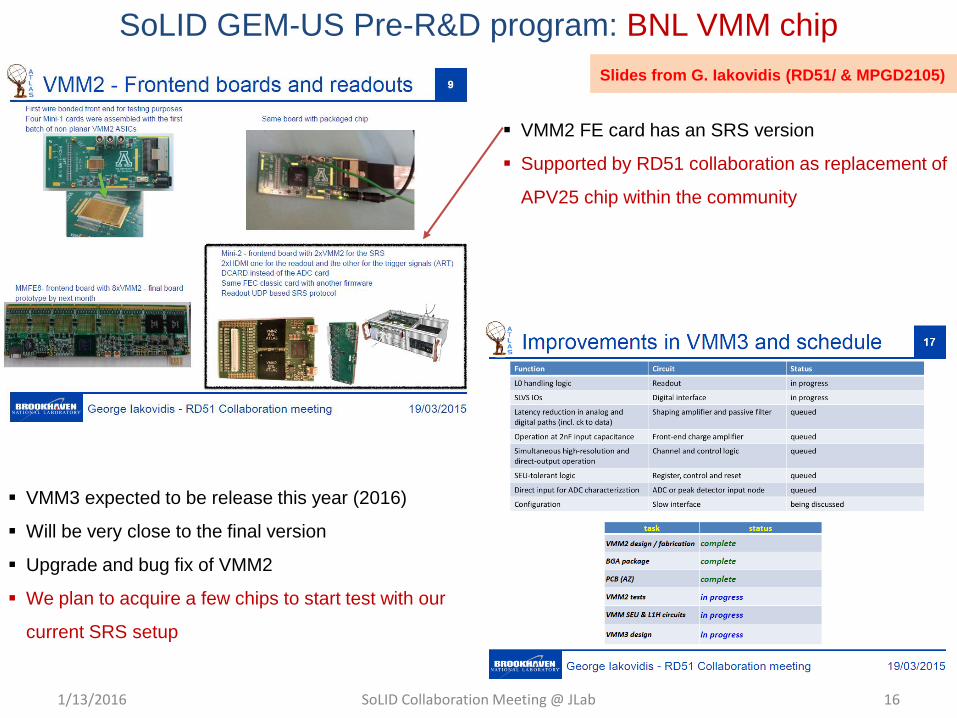
SoLID GEM-US Pre-R&D program: BNL VMM chip
1/13/2016 16
VMM2 FE card has an SRS version
Supported by RD51 collaboration as replacement of
APV25 chip within the community
VMM3 expected to be release this year (2016)
Will be very close to the final version
Upgrade and bug fix of VMM2
We plan to acquire a few chips to start test with our
current SRS setup
Slides from G. Iakovidis (RD51/ & MPGD2105)

1/13/2016 SoLID Collaboration Meeting @ JLab 17
SoLID GEM R&D activities requiring funding at UVa and TU
• Small investments in pre R&D pay big dividends at final R&D and production.
• While a significant progress towards SoLID GEMs accomplished within the EIC R&D program some SoLID specific funding needed.
• Following is a rough estimate for the first year of SoLID GEM pre-R&D
• UVa $ 20 k :
• Components and manpower for a Solid prototype design.
• TU $ 20 k:
• Design and fabrication costs for SoLID specific GEM foils and chamber components.
• UVa/TU $ 40 k:
• Funds to host Chinese collaborators for extended visits.
• Purchase single mask foils from CIAE and build and characterize prototypes.
SoLID Collaboration Meeting @ JLab
Summary / Outlook
1/13/2016 18
Large GEM activities in US (UVa & Temple U)
Production of Large Area GEM trackers for the SBS in Hall A and PRad in Hall B
Ongoing intensive GEM R&D for the EIC forward tracking
Multi-Institute collaboration for development of MPGD technologies
Effort to promote domestic production of GEM with Tech Etch (B. Surrow, Temple U)
Progress in the integration of the APV-25 readout electronics into Jlab CODA DAQ
Both APV-SRS and APV-MPD Electronics will be used in beam at JLab in 2016
SoLID GEM-US program for a two years pre-R&D
Finalize the design of SoLID GEM modules for all configuration
Setup a program to start testing and characterization of Chinese GEM foils
Construction of full size prototypes of the
Investigate needs and option for SoLID GEM readout electronics
Study the currently available candidate such as BNL VMM or Saclay DREAM chip
SoLID Collaboration Meeting @ JLab
Back Up
1/13/2016 19

SoLID Collaboration Meeting @ JLab
Overview of SoLID GEM Trackers: PVDIS Configuration
1/13/2016 20
Instrument five locations with GEMs:
30 GEM modules at each location: each module with a 12-degree angular width.
Largest GEM module size required: 113 cm x (21-44) cm
With ~5% spares, we will need about 170 k readout channels.
Large number of readout channels; but cost of electronics going down – cost per channel for the
RD51 SRS APV-25 based readout is ~ $3.00 + R&D expenses to optimize electronics for SoLID
needs.

SoLID Collaboration Meeting @ JLab
Overview of SoLID GEM Trackers: SIDIS Configuration
1/13/2016 21
Six locations instrumented with GEM trackers:
PVDIS GEMs can be re-arranged to make all layers for SIDIS by moving the modules closer to
the axis so that they are overlapping with each other
Plane Z (cm) RI (cm)RO
(cm)Active
area (m2)# of
channels
1 -175 36 87 2.0 24 k
2 -150 21 98 2.9 30 k
3 -119 25 112 3.7 33 k
4 -68 32 135 5.4 28 k
5 5 42 100 2.6 20 k
6 92 55 123 3.8 26 k
total: ~20.4 ~ 161 k
PVDIS
SIDIS
The idea of using the same modules for different configurations need to be evaluated
Might not necessarily be optimal in term of cost production and best design for the experiment

1/13/2016 SoLID Collaboration Meeting @ JLab 22
Temple University GEM R&D program
Major effort on STAR Forward GEM Tracker completed with full installation in fall 2012 - 24 large
triple-GEM detectors arranged on disks / 30720 channels (APV25-S1)
Large group at TU with fully equipped micro-pattern detector laboratory (Detector lab and
permanent clear room facility) at new Science Education and Research Center with outstanding
resources
Major funded EIC R&D effort on large triple-GEM detectors focusing on light-weight structures
and commercial fabrication of various detector components
Slides provided by Bernd Surrow


