Solder Alloy Choice for Through Hole Ceramic Discoidal ... · between the shrinkage amount and rate...
26
AN0011 – Issue 8 CN# P109953 Solder Alloy Choice for Through Hole Ceramic Discoidal & Planar Array Capacitors Introduction ............................................................................................2 Introduction to through hole ceramic capacitors ...........................................3 General soldering trials .............................................................................5 Investigation into cause of cracks...............................................................7 Solder alloy trials .....................................................................................8 1) Solder Type 62Sn/36Pb/2Ag ..................................................................9 2) Solder Type 60Sn/40Pb.........................................................................10 3) Solder Type 99.3Sn/0.7Cu ....................................................................11 4) Solder Type 95.5Sn/3.8Ag/0.7Cu ...........................................................12 5) Solder Type 50In / 50Pb .......................................................................13 6) Solder Type 95Pb / 5In .........................................................................14 7) Solder Type 93.5Pb/5Sn/1.5Ag ..............................................................15 Results Summary .....................................................................................16 Demonstration of effect with PdAg termination ............................................17 Testing PdAg termination and Pb free solder alloy ........................................18 Analysis of the Cause of failure ..................................................................20 Analysis of the differences between gold plate and PdAg terminations ............22 Comments on fritted termination in discoidal and planar capacitors ................24 Conclusions .............................................................................................25 RoHS compliance .....................................................................................26 Knowles UK Limited, Old Stoke Road, Arminghall, Norwich, Norfolk, NR14 8SQ, United Kingdom Tel: +44 (0) 1603 723300 Tel. (Sales): 01603 723310 Fax: +44 (0) 1603 723301 Email: [email protected] Web: www.knowlescapacitors.com
Transcript of Solder Alloy Choice for Through Hole Ceramic Discoidal ... · between the shrinkage amount and rate...
AN0011 – Issue 8 CN# P109953
Solder Alloy Choice for Through Hole Ceramic Discoidal & Planar Array
Capacitors
Introduction ............................................................................................2
Introduction to through hole ceramic capacitors ...........................................3
General soldering trials .............................................................................5
Investigation into cause of cracks ...............................................................7
Solder alloy trials .....................................................................................8
1) Solder Type 62Sn/36Pb/2Ag ..................................................................9
2) Solder Type 60Sn/40Pb.........................................................................10
3) Solder Type 99.3Sn/0.7Cu ....................................................................11
4) Solder Type 95.5Sn/3.8Ag/0.7Cu ...........................................................12
5) Solder Type 50In / 50Pb .......................................................................13
6) Solder Type 95Pb / 5In .........................................................................14
7) Solder Type 93.5Pb/5Sn/1.5Ag ..............................................................15
Results Summary .....................................................................................16
Demonstration of effect with PdAg termination ............................................17
Testing PdAg termination and Pb free solder alloy ........................................18
Analysis of the Cause of failure ..................................................................20
Analysis of the differences between gold plate and PdAg terminations ............22
Comments on fritted termination in discoidal and planar capacitors ................24
Conclusions .............................................................................................25
RoHS compliance .....................................................................................26
Knowles UK Limited, Old Stoke Road, Arminghall, Norwich, Norfolk, NR14 8SQ, United Kingdom Tel: +44 (0) 1603 723300 Tel. (Sales): 01603 723310 Fax: +44 (0) 1603 723301 Email: [email protected] Web: www.knowlescapacitors.com

Application Note
Reference No: AN0011
Solder Alloy Choice for
Through Hole Ceramic
Discoidal & Planar Array
Capacitors Issue 8
Page 2 of 26
Introduction
It has been well known for a number of years that solder alloy choice is a critical factor in soldering
to ceramic discoidal and planar array capacitors and that conventional SnPb solders have the
potential to cause problems with micro-cracking of the capacitors ceramic structure. For this
reason it has been common to use special solder alloys with high ductility to allow stress relief
within the solder joint for this type of product.
The introduction of lead free solder alloys as a result of the EU ‘RoHS’ directive and other similar
directives around the world has prompted further investigation into this phenomenon to categorise
the effects of these alloys.
This application note aims to demonstrate the effect the choice of solder alloy has when soldering
to the internal bore of these through hole capacitors.

Application Note
Reference No: AN0011
Solder Alloy Choice for
Through Hole Ceramic
Discoidal & Planar Array
Capacitors Issue 8
Page 3 of 26
Introduction to through hole ceramic capacitors
Through hole ceramic capacitors are based on the technology of multi layer chip capacitors (MLCC’s)
with modified internal architecture. The manufacture is similar to MLCC’s in that layers of ceramic
dielectric material interlaced with precious metal electrodes are built up to form the structure, but
holes are then drilled in the ceramic to form contacts to the inner or hot electrodes. The outside is
machined to shape and makes contact to the outer or cold electrodes. The capacitance is formed
between the hole and the outside edge. In the case of planar arrays, capacitance is formed between
each hole and the outside edge. Within limits, each hole can have different capacitance characteristics.
Single hole devices are usually referred to as discs (they are not necessarily circular) whilst multi hole
devices are referred to as planar arrays.
The materials involved are typically BaTiO3 ceramic dielectric with PdAg electrodes. Terminations are
usually plated Au over Ni directly onto the ceramic surface, or sometimes PdAg based fritted glass
solderable terminations.
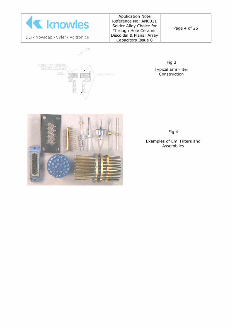
The finished capacitor device is used in the assembly of EMI filters and filter assemblies. Their special
construction allows the devices to have superior high frequency performance to SM chip based filtering
– important for applications such as military, aeronautical and medical. For the construction of an EMI
filter, the discoidal or array is soldered into a carrying can, or body, with a pin soldered through the
centre. The assembly can then be encapsulated to give improved mechanical and environmental
protection. The signal to be filtered is passed through the pin and the outside of the body connected to
earth.
The pin and body are usually manufactured from Cu or Cu based alloys, plated with Ag or Au.
Fig 2
Examples of Discoidal and
Planar Array Capacitors
Fig 1
Typical Discoidal Construction
Internal electrode Structure
Metallised or
plated termination
area
Application Note
Reference No: AN0011
Solder Alloy Choice for
Through Hole Ceramic
Discoidal & Planar Array
Capacitors Issue 8
Page 4 of 26
Fig 3
Typical Emi Filter Construction
Fig 4
Examples of Emi Filters and Assemblies

Application Note
Reference No: AN0011
Solder Alloy Choice for
Through Hole Ceramic
Discoidal & Planar Array
Capacitors Issue 8
Page 5 of 26
General soldering trials
It has been acknowledged for some years that soldering to the internal bore of the capacitor had the
potential to induce cracks within the ceramic structure. The cracks generated by this process are
known as ‘Longbow’ or ‘Comma’ cracks from their distinctive shape when viewed from a side cross
section or top cross section respectively.
These cracks can be benign or can cause total electrical failure, dependant on whether they pass
through the area of electrode overlap. Possibly of more concern, the cracks can be instigated during
soldering, but only propagate during further processing or in use, whereupon the capacitor can fail in
operation.
Capacitor failure will always tend towards a short circuit. If there is sufficient electrical power
available, the part will then become extremely hot and can represent a source of combustion.
Cracks in the dielectric material can result in catastrophic electrical breakdown of the capacitor if they
propagate through the active electrode area. Cracks are considered quality defects and cannot be
accepted for high performance applications.
Fig 5
‘Longbow Crack’
Capacitor soldered using
inappropriate solder alloy. Crack
in dielectric material generated
during cooling of solder joint after reflow.
CERAMIC CAPACITOR
COPPER ALLOY PIN
SOLDER JOINT CRACKS
Fig 6
‘Comma Crack’
The same crack as in Fig 3
above, but sectioned through a plane 90º displaced.
COPPER ALLOY PIN
SOLDER JOINT
CRACKS
CERAMIC CAPACITOR
Application Note
Reference No: AN0011
Solder Alloy Choice for
Through Hole Ceramic
Discoidal & Planar Array
Capacitors Issue 8
Page 6 of 26
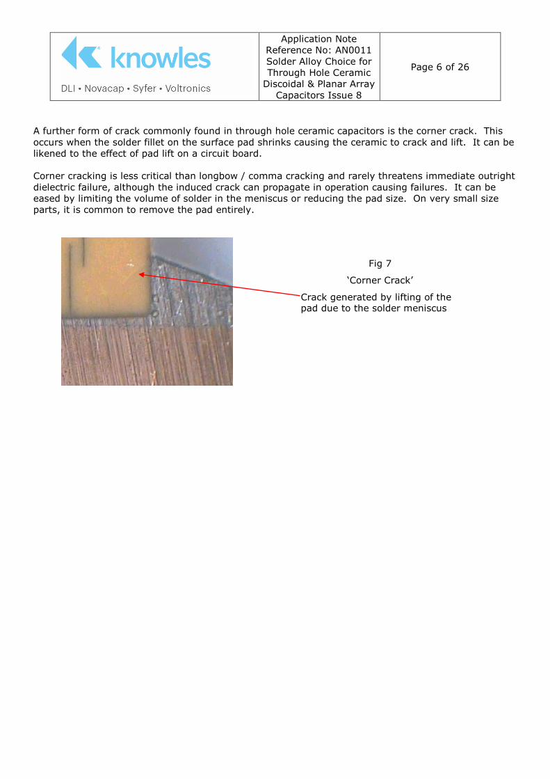
A further form of crack commonly found in through hole ceramic capacitors is the corner crack. This
occurs when the solder fillet on the surface pad shrinks causing the ceramic to crack and lift. It can be
likened to the effect of pad lift on a circuit board.
Corner cracking is less critical than longbow / comma cracking and rarely threatens immediate outright
dielectric failure, although the induced crack can propagate in operation causing failures. It can be
eased by limiting the volume of solder in the meniscus or reducing the pad size. On very small size
parts, it is common to remove the pad entirely.
Fig 7
‘Corner Crack’
Crack generated by lifting of the pad due to the solder meniscus
Application Note
Reference No: AN0011
Solder Alloy Choice for
Through Hole Ceramic
Discoidal & Planar Array
Capacitors Issue 8
Page 7 of 26
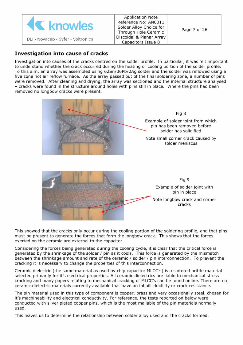
Investigation into cause of cracks
Investigation into causes of the cracks centred on the solder profile. In particular, it was felt important
to understand whether the crack occurred during the heating or cooling portion of the solder profile.
To this aim, an array was assembled using 62Sn/36Pb/2Ag solder and the solder was reflowed using a
five zone hot air reflow furnace. As the array passed out of the final soldering zone, a number of pins
were removed. After cleaning and drying, the array was sectioned and the internal structure analysed
– cracks were found in the structure around holes with pins still in place. Where the pins had been
removed no longbow cracks were present.
This showed that the cracks only occur during the cooling portion of the soldering profile, and that pins
must be present to generate the forces that form the longbow crack. This shows that the forces
exerted on the ceramic are external to the capacitor.
Considering the forces being generated during the cooling cycle, it is clear that the critical force is
generated by the shrinkage of the solder / pin as it cools. This force is generated by the mismatch
between the shrinkage amount and rate of the ceramic / solder / pin interconnection. To prevent the
cracking it is necessary to change the properties of this interconnection.
Ceramic dielectric (the same material as used by chip capacitor MLCC’s) is a sintered brittle material
selected primarily for it’s electrical properties. All ceramic dielectrics are liable to mechanical stress
cracking and many papers relating to mechanical cracking of MLCC’s can be found online. There are no
ceramic dielectric materials currently available that have an inbuilt ductility or crack resistance.
The pin material used in this type of component is copper, brass and very occasionally steel, chosen for
it’s machineability and electrical conductivity. For reference, the tests reported on below were
conducted with silver plated copper pins, which is the most mallable of the pin materials normally
used.
This leaves us to determine the relationship between solder alloy used and the cracks formed.
Fig 8
Example of solder joint from which
pin has been removed before
solder has solidified
Note small corner crack caused by solder meniscus
Fig 9
Example of solder joint with
pin in place
Note longbow crack and corner cracks

Application Note
Reference No: AN0011
Solder Alloy Choice for
Through Hole Ceramic
Discoidal & Planar Array
Capacitors Issue 8
Page 8 of 26
Solder alloy trials
To analyse the effects of different solder alloys, a set of trials were carried out using the following
alloys:
62Sn/36Pb/2Ag Traditional LMP solder
60Sn/40Pb Traditional solder
99.3Sn/0.7Cu Lead free ‘plumbers’ solder
95.5Sn/3.8Ag/0.7Cu Lead free solder recommended for PCB assembly
50Pb/50In Ductile stress relieving solder
95Pb/5In Ductile stress relieving HMP solder
93.5Pb/5Sn/1.5Ag Ductile stress relieving HMP solder
This matrix represents the solders currently in use for the assembly of EMI filters, conventional tin lead
solders and samples of lead free proposed replacement solders.
In each case except the 2 HMP alloys, two sample sets of filters were assembled and reflowed using a
five zone hot air reflow furnace. Sample 1 had a standard solder profile with forced cooling by air
blowers after zone 5. Sample 2 was reflowed using the same soldering profile but with the cooling air
blowers turned off to allow gradual cooling, so as to reduce the stresses on the ceramic.
95Pb/5In solder has a high melting point of 300ºC/313ºC, and 93.5Pb/5Sn/1.5Ag a high melting point
of 296ºC/301ºC, so neither could be soldered using the available hot air furnace. Instead samples of
these were assembled using a hot plate at 425ºC. Preheat was not used. Sample 1 parts were force
cooled by placing directly in front of a desk fan. Sample 2 parts were allowed to gradually cool.
The samples were then sectioned, allowing the capacitor structure around the solder joints to be
inspected for cracking.

Application Note
Reference No: AN0011
Solder Alloy Choice for
Through Hole Ceramic
Discoidal & Planar Array
Capacitors Issue 8
Page 9 of 26
Results
1) Solder Type 62Sn/36Pb/2Ag
Sample 1 (Forced cooling)
80% of the joints sectioned had longbow cracks adjacent to the solder joint. All the
joints inspected had some cracking present in the ceramic, mostly corner cracks..
Sample 2 (Gradual cooling)
20% of the joints sectioned had longbow cracks adjacent to the solder joint. A total of
60% of joints had corner cracks associated with the solder meniscus.
Fig 11
Example of 62Sn/36Pb/2Ag
solder joint showing longbow and corner cracks
Fig 10
Example of force cooled
62Sn/36Pb/2Ag solder joint
showing longbow and corner cracks

AN0011 – Issue 8 CN# P109953
2) Solder Type 60Sn/40Pb
Sample 1 (Forced cooling)
All of the joints sectioned had longbow cracks adjacent to the solder joint. All joints also
has corner cracks.
Sample 2 (Gradual cooling)
60% of the joints sectioned exhibited longbow cracks adjacent to the solder joint. A
total of 80% of joints had corner cracks associated with the solder meniscus.
Fig 13
Example of 60Sn/40Pb solder
joint showing longbow and corner cracks
Fig 12
Example of force cooled
60Sn/40Pb solder joint
showing longbow and corner cracks

AN0011 – Issue 8 CN# P109953
3) Solder Type 99.3Sn/0.7Cu
Sample 1 (Forced cooling)
All of the joints sectioned had longbow cracks adjacent to the solder joint. All joints also
has corner cracks.
Sample 2 (Gradual cooling)
All of the joints sectioned had longbow cracks adjacent to the solder joint. All joints also
has corner cracks.
Fig 15
Example of 99.3Sn/0.7Cu
solder joint showing longbow and corner cracks
Fig 14
Example of force cooled
99.3Sn/0.7Cu solder joint
showing longbow and corner cracks

Application Note
Reference No: AN0011
Solder Alloy Choice for
Through Hole Ceramic
Discoidal & Planar Array
Capacitors Issue 8
Page 12 of 26
4) Solder Type 95.5Sn/3.8Ag/0.7Cu
Sample 1 (Forced cooling)
All of the joints sectioned had longbow cracks adjacent to the solder joint. All joints also
has corner cracks.
Sample 2 (Gradual cooling)
40% of the joints sectioned had longbow cracks adjacent to the solder joint. 80% of the
joints in total had corner cracks, mainly corner cracks associated with solder pads.
Fig 17
Example of 95.5Sn/3.8Ag/0.7Cu
solder joint showing longbow and corner cracks
Fig 16
Example of force cooled
95.5Sn/3.8Ag/0.7Cu solder
joint showing longbow and corner cracks

AN0011 – Issue 8 CN# P109953
5) Solder Type 50In / 50Pb
Sample 1 (Forced cooling)
None of the joints sectioned exhibited any sign of induced cracks in the ceramic.
Sample 2 (Gradual cooling)
None of the joints sectioned exhibited any sign of induced cracks in the ceramic.
Fig 19
Example of 50Pb/50In solder
joint showing absence of any cracks
Fig 18
Example of force cooled
50Pb/50In solder joint
showing absence of any
cracks

Application Note
Reference No: AN0011
Solder Alloy Choice for
Through Hole Ceramic
Discoidal & Planar Array
Capacitors Issue 8
Page 14 of 26
6) Solder Type 95Pb / 5In
Sample 1 (Forced cooling)
None of the joints sectioned exhibited any sign of induced cracks in the ceramic.
Sample 2 (Gradual cooling)
None of the joints sectioned exhibited any sign of induced cracks in the ceramic.
Fig 20
Example of force cooled
95Pb/5In solder joint showing absence of any cracks
Fig 21
Example of 95Pb/5In solder
joint showing absence of any cracks

AN0011 – Issue 8 CN# P109953
7) Solder Type 93.5Pb/5Sn/1.5Ag
Sample 1 (Forced cooling)
10% of the joints inspected showed very small longbow cracks adjacent to the solder
joint. These were noticeably smaller than the cracks seen in other samples.
Sample 2 (Gradual cooling)
None of the joints sectioned exhibited any sign of induced cracks in the ceramic.
Fig 22
Example of 93.5Pb/5Sn/1.5Ag
solder joint showing small longbow cracks.
Fig 23
Example of 93.5Pb/5Sn/1.5Ag
solder joint showing absence of any cracks

Application Note
Reference No: AN0011
Solder Alloy Choice for
Through Hole Ceramic
Discoidal & Planar Array
Capacitors Issue 8
Page 16 of 26
Results Summary
Alloy Type Cooling % Defective
‘Longbow’ only
% Defective
Total
62Sn/36Pb/2Ag Forced 80 100
Gradual 20 60
60Sn/40Pb Forced 100 100
Gradual 60 80
99.3Sn/0.7Cu Forced 100 100
Gradual 100 100
95.5Sn/3.8Ag/0.7Cu Forced 100 100
Gradual 40 80
50Pb/50In Forced 0 0
Gradual 0 0
95Pb/5In Forced 0 0
Gradual 0 0
93.5Pb/5Sn/1.5Ag Forced 10 10
Gradual 0 0
Note:
The HMP solder joints were made using capacitors without solder pads as available jigging did
not allow padded parts to be assembled. This eliminated corner cracking and may have slightly
distorted the results with respect to this. However, the very low level of longbow cracking
found in HMP soldered parts (10% of force cooled 93.5Pb/5Sn/1.5Ag joints only) still indicates
the improved performance of these alloys.

Application Note
Reference No: AN0011
Solder Alloy Choice for
Through Hole Ceramic
Discoidal & Planar Array
Capacitors Issue 8
Page 17 of 26
Demonstration of effect with PdAg termination
PdAg terminations raise another problem with soldering to through holes in ceramic - the termination
to ceramic bond is reduced when compared to gold plating. The effect of this is that the contraction
forces tend to stress relieve the assembly at the termination / ceramic interface rather than inside the
ceramic structure in the form of a crack.
On the face of it, this may appear better than a potentially fatal crack, but it raises a potentially more
worrying concern.
If a ceramic capacitor is cracked, and subsequently fails, then the resulting fail is almost always a short
circuit IR failure. This is normally immediately apparent and the resulting failure can be isolated and
removed.
Failure of the termination / ceramic interface will tend not to cause an immediate obvious failure, but
will instead result in loss of the filtering performance, often due to dropping capacitance. There have
been cases of total loss of filtering due to total failure of the termination / ceramic interface. Loss of
filtering may not be immediately apparent, but the effect on the performance of the overall system can
be far worse.

Application Note
Reference No: AN0011
Solder Alloy Choice for
Through Hole Ceramic
Discoidal & Planar Array
Capacitors Issue 8
Page 18 of 26
Testing PdAg termination and Pb free solder alloy
To demonstrate the problems experienced with soldering to PdAg termination it is easiest to consider a
design of capacitor where the capacitance is constructed without electrodes connected to the through
hole.
The capacitance is created by the interaction of the internal bore termination and the outer earth
electrodes.
The advantage of carrying out experiments with this type of construction is that any failure of the
internal termination or ceramic cracking is demonstrated by a drop in the capacitance. This is because
of the introduction of an alternative dielectric material – air – in the area of the failure.
Tests were carried out using capacitor arrays with the electrical design shown above and terminated
with PdAg termination material. Prior to assembly, the capacitance of the holes with this design was
recorded. The assembly was soldered using 95.5Sn/3.8Ag/0.7Cu solder and hot air reflow. After
assembly, the capacitance was re-measured and the results tabulated below.
Fig 24
Typical Stray Cap. Discoidal Construction
Internal electrode Structure – Note no electrodes connected to internal bore of capacitor
Metallised or
plated termination
area

Application Note
Reference No: AN0011
Solder Alloy Choice for
Through Hole Ceramic
Discoidal & Planar Array
Capacitors Issue 8
Page 19 of 26
Test Results
Array No. 1 Array No. 2
Start
Capacitance
(pF)
Capacitance
after Soldering
(pF)
Change (%) Start
Capacitance
Capacitance
after Soldering Change (%)
551 296 -46.3 539 331 -38.6
550 242 -56.0 540 256 -52.6
550 300 -45.5 535 196 -63.4
552 249 -54.9 536 189 -64.7
553 244 -55.9 532 323 -39.3
546 474 -13.2 538 151 -71.9
544 351 -35.5 536 91 -83.0
543 418 -23.0 539 175 -67.5
551 339 -38.5 544 353 -35.1
551 520 -5.6 536 168 -68.7
546 368 -32.6 536 176 -67.2
550 289 -47.5 534 317 -40.6
544 451 -17.1 544 173 -68.2
544 443 -18.6 543 153 -71.8
550 242 -56.0 543 285 -47.5
Array No. 1 Array No. 2
Mean Drop = 36.5% Mean Drop = 58.7%
Maximum Drop = 56.0% Maximum Drop = 83.0%

Application Note
Reference No: AN0011
Solder Alloy Choice for
Through Hole Ceramic
Discoidal & Planar Array
Capacitors Issue 8
Page 20 of 26
Analysis of the Cause of failure
The capacitor arrays were surface sectioned to check for the presence of cracks in the ceramic. Using
this method of sectioning analysis allows us to investigate all solder joints at once. If cracks are found,
they will be of the ‘Comma’ variety described above.
Surface sectioning of both arrays found no ceramic cracks.
We can therefore conclude that the capacitance loss is not caused by cracks within the ceramic in the
same way that gold terminated parts are affected.
One effect that can be seen from the surface sections above is that of solder / termination pull – away
from the bore of the ceramic. This has the same effect as the cracks in gold plated parts, introducing a
section of air dielectric within the capacitor build.
This effect can be seen in FIG 26 above. A further example is below:
Fig 25
Surface Section of Array No. 2
showing absence of damage to ceramic
Fig 26
Close-up of Surface Section of Array
No. 1 showing absence of damage to ceramic
AN0011 – Issue 8 CN# P109953
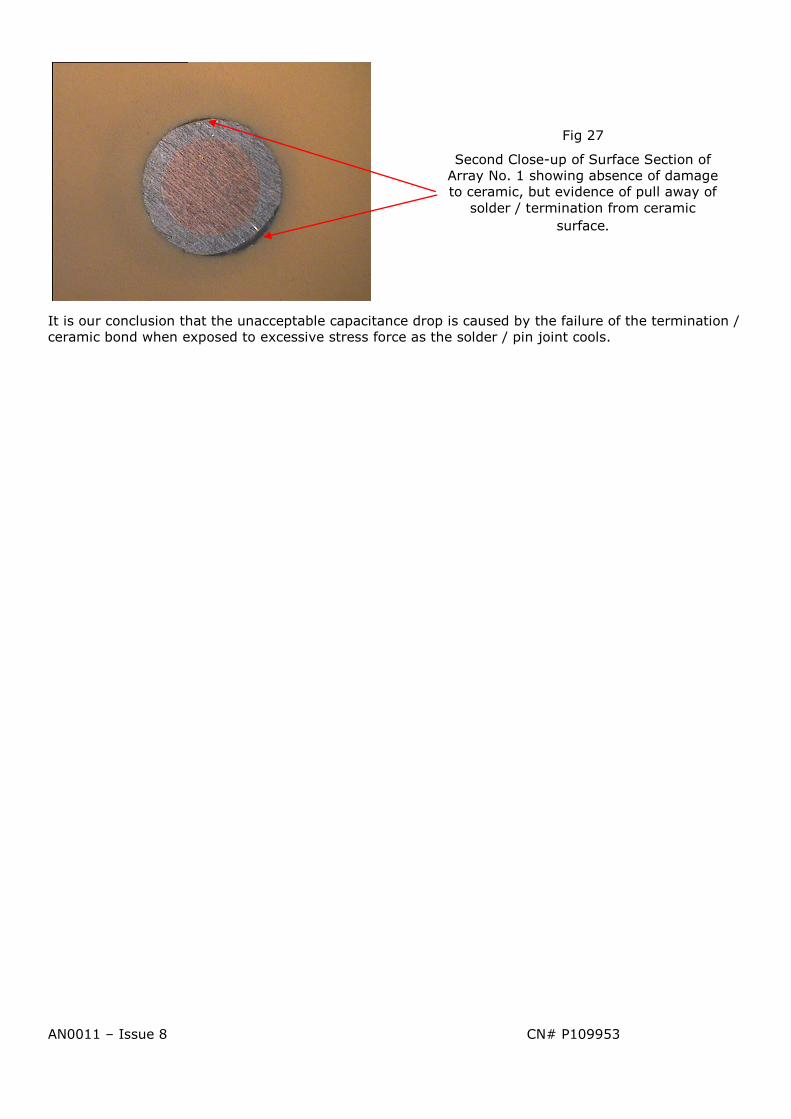
It is our conclusion that the unacceptable capacitance drop is caused by the failure of the termination /
ceramic bond when exposed to excessive stress force as the solder / pin joint cools.
Fig 27
Second Close-up of Surface Section of
Array No. 1 showing absence of damage
to ceramic, but evidence of pull away of
solder / termination from ceramic
surface.

AN0011 – Issue 8 CN# P109953
Analysis of the differences between gold plate and PdAg terminations
To understand the failure mode above, it is necessary to investigate the differences between PdAg
termination and gold plate.
1. With PdAg termination, the bond to the ceramic is far weaker than gold plate termination. This
can be demonstrated by a simple pull test, as below.
As can be seen above, the gold plated termination has a far greater adhesion to the ceramic,
demonstrated by the amount of ceramic material still attached to the pin. By comparison, the
PdAg termination has been cleanly removed from the ceramic with no ceramic material
removed. Pins 3 and 4 do show the PdAg termination still attached to the solder – identified by
the dull grey areas on the solder.
This is further shown in FIG 29, where the pins have been removed from a partially sectioned
array soldered with PdAg termination.
Fig 28
Silver plated copper pins soldered into planar array capacitors using 95.5Sn/3.8Ag/0.7Cu
solder and removed by simply pulling out using a pair of pliers.
Pins 1 & 2 have been pulled from an array terminated with gold plate.
Pins 3 & 4 have been pulled from an array terminated with PdAg fritted termination.
1
4
3
2
Fractured ceramic remaining attached to
the feedthrough pin after attempting to
pull the pin out.
On closer inspection its possible to see
the internal electrode structure of the
capacitor.
Both demonstrate the characteristic shape
of the longbow / comma crack in the way
the ceramic fractured
Remains of PdAg termination can be seen
on the otherwise ‘clean’ solder joint on
pins 3 & 4

Application Note
Reference No: AN0011
Solder Alloy Choice for
Through Hole Ceramic
Discoidal & Planar Array
Capacitors Issue 8
Page 23 of 26
The ceramic exhibits no damage, and the pins are very easily removed – the termination has
relatively little adhesion to the ceramic.
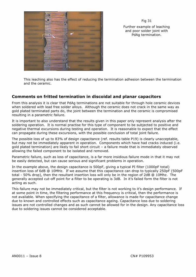
2. Secondly, PdAg termination is far more susceptible to leaching into the molten solder as the
joint is formed. In sectioned components, this is observed as areas of missing termination
within the bore of the component.
Leaching is far more common with Pb free alloys, and has been observed on PdAg terminated
components with all Pb free alloys. The following examples have been soldered using
95.5Sn/3.8Ag/0.7Cu solder alloy.
Fig 29
Example of PdAg terminated
planar array capacitor soldered
with 95.5Sn/3.8Ag/0.7Cu
solder.
As the component is sectioned,
the pins can be easily removed
without damage to the ceramic.
Note the dark grey on the solder
joint – this is the termination,
which has been removed along with the pin & solder.
Fig 30
Termination leached away
from this area.
These electrodes have lost
contact and will result in a
potential reduction in filtering performance.
AN0011 – Issue 8 CN# P109953
This leaching also has the effect of reducing the termination adhesion between the termination
and the ceramic.
Comments on fritted termination in discoidal and planar capacitors
From this analysis it is clear that PdAg terminations are not suitable for through hole ceramic devices
when soldered with lead free solder alloys. Although the ceramic does not crack in the same way as
gold plated terminated parts do, the joint between the termination and the ceramic is compromised
resulting in a parametric failure.
It is important to also understand that the results given in this paper only represent analysis after the
soldering operation. It is normal practise for this type of component to be subjected to positive and
negative thermal excursions during testing and operation. It is reasonable to expect that the effect
can propagate during these excursions, with the possible conclusion of total joint failure.
The possible loss of up to 83% of design capacitance (ref. results table P19) is clearly unacceptable,
but may not be immediately apparent in operation. Components which have had cracks induced (i.e.
gold plated termination) are likely to fail short circuit – a failure mode that is immediately observed
allowing the failed component to be isolated and removed.
Parametric failure, such as loss of capacitance, is a far more insidious failure mode in that it may not
be easily detected, but can cause serious and significant problems in operation.
In the example above, the design capacitance is 500pF, giving a typical PI filter (1000pF total)
insertion loss of 6dB @ 10MHz. If we assume that this capacitance can drop to typically 250pF (500pF
total - 50% drop), then the resultant insertion loss will only be in the region of 2dB @ 10Mhz. The
generally accepted cut-off point for a filter to be operating is 3dB. In it’s failed form the filter is not
acting as such.
This failure may not be immediately critical, but the filter is not working to it’s design performance. If
at some point in time, the filtering performance at this frequency is critical, then the performance is
not available. When specifying the capacitance of a filter, allowance is made for capacitance change
due to known and controlled effects such as capacitance ageing. Capacitance loss due to soldering
issues are not controlled changes and as such cannot be allowed for in the design. Any capacitance loss
due to soldering issues cannot be considered acceptable.
Fig 31
Further example of leaching
and poor solder joint with
PdAg termination.

Application Note
Reference No: AN0011
Solder Alloy Choice for
Through Hole Ceramic
Discoidal & Planar Array
Capacitors Issue 8
Page 25 of 26
Conclusions
1. Potentially fatal cracks were found in all assemblies manufactured with both conventional tin
lead solders and the proposed lead free alloys and gold plated termination.
2. Tin lead alloys induced cracks in the ceramic dielectric and should not be used for the
manufacture of these assemblies.
3. Lead free alloys performed worse of all solders under test, and should not be used for the
manufacture of these assemblies. The lead free alloys tended to perform worse than the tin
lead alloys – more cracks and larger cracks were found.
4. In order to manufacture reliable safe capacitor assemblies, it is essential to use a ductile solder
so as to prevent excessive force being transferred to the ceramic dielectric material. Ductile
solders tend to be an alloy of lead and indium.
5. High melting point alloys, typically containing >90% lead and melting around 300ºC, are
acceptable if indium is to be avoided - but have a narrower processing window and are more
susceptible to problems if the cooling rate is not controlled.
Obviously the use of these alloys increases the total amount of lead used in the assembly, but
also the higher soldering temperatures required mean increased energy consumption and
specialist soldering equipment. Is is often necessary to use vacuum or atmosphere systems to
prevent surface oxidisation.
6. Solder joint design should be given due consideration. In particular, solder pads should be
reduced or minimised (Note – the manufacture and testing of the capacitor itself will sometimes
demand solder pads are included)
7. Gradual cooling should be used and force cooling, either intentional or unintentional due to
factors such as drafts, should be avoided.
8. PdAg terminations reduce the incidence of ceramic cracking, but may result instead in
parametric failure of the capacitor. This can be ultimately worse in service.
9. It is clear that there is a conundrum – if the termination system provides a very good bond to
the ceramic, then there is a risk of cracking the ceramic. If the termination system provides a
weak bond to the ceramic then there is a risk of parametric failure leading to loss of
performance.
10. The best option for reliable performance is to use a termination system that provides a very
strong bond to the ceramic (e.g. gold) and introduce stress relief through the use of ductile
solders containing Lead and Indium.

Application Note
Reference No: AN0011
Solder Alloy Choice for
Through Hole Ceramic
Discoidal & Planar Array
Capacitors Issue 8
Page 26 of 26
RoHS compliance
EU directive 2011/56/EU (superseding 2002/95/EC), commonly known as RoHS directive, limits the
use of certain substances in electronics manufacture. These substances include lead, which has forced
a change from lead containing solders to lead free solders for a majority of applications.
Clearly from the evidence shown above, the use of lead free solders should be avoided when soldering
to ceramic discoidal and planar capacitors.
The directive allows for exemptions to be granted for situations where there is no technical alternative
or such alternatives constitute a negative environmental impact. Syfer have successfully applied for
the use of lead containing solders for soldering to ceramic planar arrays and discoidal capacitors to be
made exempt from the directive.
This exemption is detailed in the annex to the directive as follows:
Exemption No. 24 Lead in solders for the soldering to machined through hole discoidal and planar
array ceramic multilayer capacitors.
Issued in the addendum to directive 2002/95/EC dated 14th October 2006 and continued in the revised
directive 2011/56/EU of 1st July 2011.
To summarise – Filters, filter assemblies and filtered connectors manufactured with Syfer discoidal and
planar capacitors can be assembled using lead bearing solder alloys – i.e. InPb – to eliminate the
incidence of micro cracking due to mismatched material shrinkages and still be RoHS compliant in this
respect.