Solar Cells on the Base of Semiconductor- Insulator - InTech
36
14 Solar Cells on the Base of Semiconductor- Insulator-Semiconductor Structures Alexei Simaschevici, Dormidont Serban and Leonid Bruc Institute of Applied Physics, Academy of Sciences, Moldova 1. Introduction The conventional energy production is not based on sustainable methods, hence exhausting the existing natural resources of oil, gas, coal, nuclear fuel. The conventional energy systems also cause the majority of environmental problems. Only renewable energy systems can meet, in a sustainable way, the growing energy demands without detriment to the environment. The photovoltaic conversion of solar energy, which is a direct conversion of radiation energy into electricity, is one of the main ways to solve the above-mentioned problem. The first PV cells were fabricated in 1954 at Bell Telephone Laboratories (Chapin et al., 1954); the first applications for space exploration were made in the USA and the former USSR in 1956. The first commercial applications for terrestrial use of PV cells were ten years later. The oil crisis of 1972 stimulated the research programs on PV all over the word and in 1975 the terrestrial market exceeds the spatial one 10 times. Besides classical solar cells (SC) based on p-n junctions new types of SC were elaborated and investigated: photoelectrochemical cells, SC based on Schottky diodes or MIS structures and semiconductor-insulator-semiconductor (SIS) structures, SC for concentrated radiation, bifacial SC. Currently, researchers are focusing their attention on lowering the cost of electrical energy produced by PV modules. In this regard, SC on the base of SIS structures are very promising, and recently the SIS structures have been recommended as low cost photovoltaic solar energy converters. For their fabrication, it is not necessary to obtain a p-n junction because the separation of the charge carriers generated by solar radiation is realized by an electric field at the insulator- semiconductor interface. Such SIS structures are obtained by the deposition of thin films of transparent conductor oxides (TCO) on the oxidized silicon surface. A overview on this subject was presented in (Malik et al., 2009). Basic investigations of the ITO/Si SIS structures have been carried out and published in the USA (DuBow et al., 1976; Mizrah et al., 1976; Shewchun et al., 1978; Shewchun et al, 1979) Theoretical and experimental aspects of the processes that take place in these structures are examined in those papers. Later on the investigations of SC based on SIS structures using, as an absorber component, Si, InP and other semiconductor materials have been continued in Japan (Nagatomo et al., 1982; Kobayashi, et al., 1991), India (Vasu & Subrahmanyam, 1992; Vasu et al., 1993), France (Manifacier & Szepessy, 1977; Caldererer et al., 1979), Ukraine www.intechopen.com
Transcript of Solar Cells on the Base of Semiconductor- Insulator - InTech

14
Solar Cells on the
Base of Semiconductor-
Insulator-Semiconductor Structures
Alexei Simaschevici Dormidont Serban and Leonid Bruc Institute of Applied Physics Academy of Sciences
Moldova
1 Introduction
The conventional energy production is not based on sustainable methods hence exhausting the existing natural resources of oil gas coal nuclear fuel The conventional energy systems also cause the majority of environmental problems Only renewable energy systems can meet in a sustainable way the growing energy demands without detriment to the environment The photovoltaic conversion of solar energy which is a direct conversion of radiation energy into electricity is one of the main ways to solve the above-mentioned problem The first PV cells were fabricated in 1954 at Bell Telephone Laboratories (Chapin et al 1954) the first applications for space exploration were made in the USA and the former USSR in 1956 The first commercial applications for terrestrial use of PV cells were ten years later The oil crisis of 1972 stimulated the research programs on PV all over the word and in 1975 the terrestrial market exceeds the spatial one 10 times Besides classical solar cells (SC) based on p-n junctions new types of SC were elaborated and investigated photoelectrochemical cells SC based on Schottky diodes or MIS structures and semiconductor-insulator-semiconductor (SIS) structures SC for concentrated radiation bifacial SC Currently researchers are focusing their attention on lowering the cost of electrical energy produced by PV modules In this regard SC on the base of SIS structures are very promising and recently the SIS structures have been recommended as low cost photovoltaic solar energy converters For their fabrication it is not necessary to obtain a p-n junction because the separation of the charge carriers generated by solar radiation is realized by an electric field at the insulator-semiconductor interface Such SIS structures are obtained by the deposition of thin films of transparent conductor oxides (TCO) on the oxidized silicon surface A overview on this subject was presented in (Malik et al 2009) Basic investigations of the ITOSi SIS structures have been carried out and published in the USA (DuBow et al 1976 Mizrah et al 1976 Shewchun et al 1978 Shewchun et al 1979) Theoretical and experimental aspects of the processes that take place in these structures are examined in those papers Later on the investigations of SC based on SIS structures using as an absorber component Si InP and other semiconductor materials have been continued in Japan (Nagatomo et al 1982 Kobayashi et al 1991) India (Vasu amp Subrahmanyam 1992 Vasu et al 1993) France (Manifacier amp Szepessy 1977 Caldererer et al 1979) Ukraine
wwwintechopencom
Solar Cells ndash Silicon Wafer-Based Technologies
300
(Malik et al 1979 Malik et al 1980) Russia (Untila et al 1998) the USA (Shewchun et al 1980 Gessert et al 1990 Gessert et al 1991) Brasil (Marques amp Chambouleyron 1986) and the Republic of Moldova (Adeeb et al 1987 Botnariuc et al 1990 Gagara et al 1996 Simashkevich et al 1999) The results of SIS structures fabrication by different methods especially by pyrolitic pulverization and radiofrequency sputtering are discussed in those papers The investigation of electrical and photoelectrical properties of the Si based SIS structures shows that their efficiency is of the order of 10 for laboratory-produced samples with an active area that does not exceed a few square centimeters The spray deposition method of ITO layer onto the silicon crystal surface results in an efficient junction only in the case of n-type Si crystals whereas in the case of p-type silicon crystals radiofrequency sputtering must be used to obtain good results Bifacial solar cells (BSC) are promising devices because they are able to convert solar energy coming from both sides of the cell thus increasing its efficiency Different constructions of BSC have been proposed and investigated In the framework of the classification suggested in (Cuevas 2005) the BSC structures could be divided into groups according to the number of junctions a) two p-n junctions b) one p-n junction and one high-low junction and c) just one p-n junction In all those types of BSC are based on a heteropolar p-n junction In this case it is necessary to obtain two junctions a heteropolar p-n junction at the frontal side of the silicon wafer and a homopolar nn+ or pp+ junction at its rear side Usually these junctions are fabricated by impurity diffusion in the silicon wafer The diffusion takes place at temperatures higher than 8000C and requires special conditions and strict control In the case of the back surface field (BSF) fabrication these difficulties increase since it is necessary to carry out the simultaneous diffusion of impurities that have an opposite influence on the silicon properties Therefore the problem arises concerning the protection of silicon surface from undesirable impurities The main purpose of this overview is to demonstrate the possibility to manufacture on the base of nSi monofacial as well as a novel type of bifacial solar cells with efficiencies over 10 containing only homopolar junctions with an enlarged active area using spray pyrolysis technique the simplest method of obtaining SIS structures with a shallow junction The utilization of such structures removes a considerable part of the above-mentioned problems in BSC fabrication The results of the investigations of ITOpInP SC obtained by spray pyrolysis are also discussed
2 The history of semiconductor-insulator-semiconductor solar cells
First it must be noted that SC obtained on the base of MIS and SIS structures are practically the same type of SC even though they are sometimes considered as being different devices The similarity of these structures was demonstrated experimentally and theoretically for two of the most common systems AlSiOxpSi and ITOSiOxpSi (Schewchun et al 1980) The tunnel current through the insulator layer at the interface is the transport mechanism between the metal or oxide semiconductor and the radiation-absorbing semiconductor silicon in this case One of the main advantages of SIS based SC is the elimination of high temperature diffusion process from the technological chain the maximum temperature at the SIS structure fabrication not being higher than 450oC The films can be deposited by a variety of techniques among which the spray deposition method is particularly attractive since it is simple relatively fast and vacuumless (Chopra et al 1983) Besides the superficial layer of
wwwintechopencom
Solar Cells on the Base of Semiconductor-Insulator-Semiconductor Structures
301
the silicon wafer where the electrical field is localized is not affected by the impurity diffusion The TCO films with the band gap of the order of 33-37eV are transparent in the whole region of solar spectrum especially in the blue and ultraviolet regions which increase the photoresponce comparative to the traditional SC The TCO layer assists with the collection of separated charge carriers and at the same time is an antireflection coating In SC fabrication the most utilized TCO materials are tin oxide indium oxide and their mixture known as indium tin oxide (ITO) Thin ITO layers have been deposited onto different semiconductors to obtain SIS structures Si (Malik et al 1979) InP (Botnariuc et al 1990) CdTe (Adeeb et al 1987) GaAs (Simashkevich et al 1992) Therefore solar cells fabricated on the base of SIS structures have been recommended as low cost photovoltaic solar energy converters The reduction in cost of such solar cells is due to the simple technology used for the junction fabrication The separation of light generated carriers is achieved by a space charge region that in the basic semiconductor is near the insulator layer The number of publications concerning the fabrication and investigation of SIS structures is very big therefore we will limited our consideration of the given structures only to those on the base of the most widespread solar materials ndash silicon and indium phosphide To be exact main attention will be focused on SC on the base of ITOnSi and ITOpInP
21 SIS structures on the base of silicon crystals As shown above one of the ways to solve the problem of the cost reduction of the electrical energy provided by SC is to use SIS structures First publications regarding the obtaining and investigation of ITOnSi structures appeared in 1976 (Mizrah amp Adler 1976) Power conversion efficiencies of 1 were reported for an ITOnSi cell obtained by the magnetron dispersion of ITO layers on the surface of nSi crystals with an active area of 013 cm2 The data obtained from the investigated I-V dark characteristics and known band gaps and the work functions of ITO and Si allows to make the band diagram of these structures (Fig 1) The efficiency of 10 was observed for ITOnSi cells obtained by the spray deposition of ITO layers onto nSi crystals with the area of 01 cm2 (Manifacier amp Szepessy 1977 Calderer et al 1979) ITOnSi SC with the power conversion efficiencies of 10 were fabricated by deposition onto n-type Si crystals by the electron- beam evaporation of a mixture of 9010 molar In2O3 SnO2 powder (Feng et al 1979) The results of those works have been analyzed in detail (Shewchun et al 1978 Shewchun et al 1979) from both experimental and theoretical points of view Given the general theory of heterojunctions is incomprehensible how they can work as effective SC formed by materials with different crystalline types and lattice constants when an intermediate layer with many defects appears at the interface It is intriguing to note here that various authors have received quite contradictory results Examining these data authors in (Shewchun et al 1979) concluded that the performance of those SC depended on the intermediate thin insulator layer Its main function is the compensation of the defects due to the mismatches of the crystalline lattices Its thickness is not greater than 30Aring which ensures the tunnel transport of the carriers through the barrier The theoretical analysis of ITOnSi solar cell has shown that they are similar to MIS structures their parameters depend on the thickness of the insulating layer at the interface the substrate doping level concentration of surface states oxide electric charge and temperature The optimization of these parameters can provide 20 efficiency In (Shewchun et al 1979) this issue was examined in terms of energy losses during conversion of sunlight into electricity Different mechanisms of energy loss that limit
wwwintechopencom
Solar Cells ndash Silicon Wafer-Based Technologies
302
ITOnSi solar cell efficiency are probably valid for other SIS structures too Dark current-voltage characteristics were used as experimental material and it was shown that after a certain threshold of direct voltage these characteristics do not differ from similar characteristics of p-n junctions in silicon and the current is controlled by diffusion processes in silicon volume Different mechanisms of energy loss that limit ITOnSi solar cell efficiency are presented in Table 1 (Shewchun et al 1979)
Fig 1 Energy band diagram of the ITOnSin +Si structure (a) - in the dark (b) - at solar illumination under open circuit conditions The shaded area - the insulating SiOx layer
wwwintechopencom
Solar Cells on the Base of Semiconductor-Insulator-Semiconductor Structures
303
Mechanism Loss rate
1 Absorption and reflection in the ITO layer up to 8
2 Recombination in space charge region 01 1
3 VCD height reduction 0 ndash 12
too high work function 0-3
inhomogeneous SiOx layer 0-3
low doped ITO layer 0-3
too large saturation current 0-3
4 Low fill factor 0-10
series resistance of the intermediate layer
series resistance of the contacts
shunt
Table 1 The energy loss mechanisms which do not provide the maximum possible efficiency of 20
An increase of the conversion efficiency of SC based on ITOnSi structures can be achieved by the optimization of the thickness of the frontal ITO layer and of the insulator SiO2 layer the optimization of the concentration of electrons in absorbing Si wafers the texturing of the Si wafers surface The thickness of the frontal ITO layer is a very important factor because it affects the quantity of the absorbed solar radiation depending on both absorption and reflection It is necessary to select such ITO layer thickness that determines a large minimum of the reflection in the region of maximum sensitivity of the n+ITOSiO2nSi SC At the same time the thickness of the frontal ITO layer determines their electrical resistance and therefore the value of the photocurrent but for all that the growing of the ITO layer thickness has an contrary effect on the solar cells efficiency diminishing the absorption and increasing the photocurrent At the same time the thickness of the frontal ITO layer determines the efficiency of this layer as an anti reflection coating The properties of the SIS structures largely also depend on the thickness of the SiO2 insulator layer at ITOSi interface This SiO2 layer increases the height of the junction potential barrier and diminishes the saturation current Besides the insulator SiO2 layer must be tunnel transparent for charge carrier transport The optimal SiO2 insulator layer thickness must be not more than some tens of Aring All silicon wafers must be oriented in the (100) plane because only such crystallographic orientation could be used to get a potential barrier by ITO spray deposition Single crystalline Si wafers with different carrier concentration from 1015cm-3 up to 1018cm-3 have been used to fabricate ITOnSi SIS structures by spray deposition The influence of the structural state of the Si single crystalline wafers on the conversion efficiency will be discussed in the next section of this overview The paper (Feng et al 1979) studied the current transport mechanism of ITOSi structures the TCO layer beings obtained by evaporation under the action of an electron beam Pre-treatment of Si crystals with Cl2 has led to the increased yield from 23 to 55 In this case the current transport mechanism was dominated by recombination in the space charge
wwwintechopencom
Solar Cells ndash Silicon Wafer-Based Technologies
304
layer while there is the thermo emission over the potential barrier in the absence of Cl2 Systematical studies of the properties of the ITOnSi structures obtained by spray pyrolysis were carried out in 1980 (Ashok et al 1980) The optical and electrical characteristics of the IT0 layer as well as the thickness of the insulator layer have been optimized to yield the following photovoltaic parameters on 05Ohmmiddotcm nSi Voc= 052V Jsc=315mAcm2 FF=070 conversion efficiency is 115 The dark I-V and C-V characteristics have also been evaluated to identify the mechanisms of barrier formation and current flow C-V data indicate an abrupt heterojuncton while dark I-V characteristics are suggestive of a tunneling process to determine current flow in these devices in conformity with the Riben and Feucht model (Riben amp Feucht 1966) A comparison of spray deposited ITOnSi and SnO2nSi was presented by Japanese researchers (Nagatomo et al 1982) The diode and photovoltaic properties of these structures are very similar but the conversion efficiency of ITOnSi is higher up to 11-13 whereas for SnO2nSi these values do not exceed 72 (Nagatomo et al 1979) As is reported in the paper (Malik et al 2008 Malik et al 2009) the authors fabricated ITOnSi solar cells using n-type single crystalline silicon wafers with a 10Ohmmiddotcm resistivity and an 80nm thick ITO film with a sheet resistance of 30Ohm that was deposited by spray pyrolysis on the silicon substrate treated in the H2O2 solution This ITO thickness was chosen in order to obtain an effective antireflection action of the film The cells obtained in such a way can be considered as structures presenting an inverted p-n junction (Fig 2)
Fig 2 Energy diagram (in kT units) of the heavy doped ITOn-Si heterojunction
Under the AM0 and AM15 solar illumination conditions the efficiency is 108 and 122 respectively The theoretical modeling based on p-n solar cells shows an excellent agreement between the theoretical and the experimental results It is also shown that using 1Ωmiddotcm silicon substrates is a promising alternative for obtaining solar cells with 14 efficiency under AM15 illumination conditions Various models for energetic band diagrams and the carrier transport mechanism in SIS ITOnSi cells have been proposed so far Among them are the thermo ionic emission as the dominant charge transport mechanism in the SC obtained by spray deposition of SnO2 onto nSi crystals (Kato et al 1975) and the recombination current in the depletion layer for the CVD deposited ITOnSi junction (Varma et al 1984) Majority of authors suggested that
wwwintechopencom
Solar Cells on the Base of Semiconductor-Insulator-Semiconductor Structures
305
trap ndashassisted multi step tunneling through the depletion layer is the determinant current flow mechanism (Ashok et al 1980 Saim amp Campbell 1987 Kobayashi et al 1990 Simashkevich et al 2009) The mechanism of the current transport through the potential barrier is determined by the energetic band diagram and the height of the barrier When the later is very high a physical p-n junction is formed in Si crystals near the surface (Fig 2) Otherwise the ITOnSi SC operate as MIS structures or Schottky diodes (Fig 1) Some data about the efficiencies of ITOnSi SC are presented in Table 2
References ITO deposition method Area (cm2) Eff () Note
Mizrah et al 1976 RF Sputtering 013 1
Manifacier et al 1977 Spray 15 10
Feng et al 1979 Electron beam 1 - 4 10
Calderer et al 1979 Spray 15 10
Ashok et al 1980 Spray 03 115 BSF
Nagatomo et al 1982 Spray 11-13
Gagara et al 1996 Spray 101
Vasu et al 2005 Electron beam 10 55
Malik et al 2008 Spray 1 - 4 112
Table 2 Efficiencies of ITOnSI solar cells fabricated by various deposition techniques of ITO films on smooth (non textured) Si crystal surfaces
The analysis of the works referred to shows that the conversion efficiency of ITOnSi solar cells obtained by various methods is about 10 and in some cases reaches 12 Their active area is not more than a few square centimeters which is not enough for practical application
22 ITOnSi solar cells with textured surface of Si crystalls
As can be seen from Table 1 the optical losses of ITOnSI solar cells are up to 8 other estimates show that they can exceed 10 (Garcia et al 1982) Those losses depend on the surface state of silicon wafers and can be minimized by creating a textured surface of the light absorbing semiconductor material thus reducing the reflection and increasing the absorption The texturization leads to the enlargement of the junction area of a photovoltaic cell and to the increase of the conversion efficiency The enlargement of the junction area in the case of silicon crystals is usually achieved by means of selective chemical etching in KOH (Bobeico et al 2001 Dikusar et al 2008 Simashkevich et al 2011) As a result pyramids or truncated cones with the base dimensions of 5mx5m or with a diameter of 10m on the Si surface are formed The efficiency of 126 under AM1 simulated irradiation was obtained for SnO2 PSiO2nSi SC with the active area of 2cm2(Wishwakarma et al 1993) Those cells were fabricated by deposition of SnO2 layers doped with P by CVD method on the textured surface of the Si crystals with resistivity of 01 Ohmcm SiO2 insulating layer was obtained by chemical
wwwintechopencom
Solar Cells ndash Silicon Wafer-Based Technologies
306
methods The textured surface of the Si crystals reduces the frontal reflectivity and consequently increases the short circuit current by around 10 ITOnSI obtained by spray deposition of ITO layers on nSi wafers oriented in (100) plane were obtained in Japan (Kobayashi et al 1990) The final size of the active area of the cell was 09cm x 09cm Mat-textured Si surfaces were produced by the immersion of the Si wafers in NaOH solution at 850C For so treated specimens the solar energy conversion efficiency of 13 was attained under AM1 illumination The paper (Simashkevich et al 2011) studied the properties of ITOnSi SC with improved parameters The performed optimization consists in the following the optimization of the thickness of the frontal ITO layer and of the thickness of the insulator SiO2 layer the optimization of the concentration of the electrons in absorbing Si wafers the texturing of the Si wafers surface The performed investigations make it possible to come to the following conclusions The optimum thickness of the frontal ITO layer was determined experimentally from the photoelectric investigations and is equal to 05m The SiO2 layer can be obtained by different methods In the case of fabrication n+ITOSiO2nSi solar cells by spray pyrolysis the optimal SiO2 layer thickness was obtained by a combined thermo chemical method selecting the temperature regime and the speed of the gas flow during ITO layer deposition The optimal SiO2 insulator layer thickness measured by means of ellipsometric method is about 30-40Aring To determine the optimal electron concentration ITOnSi SIS structures were investigated obtained by ITO spray deposition on the surface of phosphor and antimony doped single crystalline Si wafers with different carrier concentrations 1015cm-3 5middot1015cm-3 6middot1016cm-3 and 2middot1018cm-3 produced in Russia (STB Telecom) and Germany (Siltronix Semirep) The investigation of the electrical properties of n+ITOSiO2nSi SC shows that the optimum values of the barrier height equal to 053eV and the space charge region thickness equal to W=036m have been obtained in the case of Si crystals with the electron concentration 5middot1015cm-3 Carrier diffusion length (L) is one of the main parameters for bifacial solar cells For this silicon crystal L is about 200m The BSF region at the rear side of the cell was obtained by phosphor diffusion To enlarge the active area and reduce optical losses due to radiation reflection the active area of Si wafer oriented in a plane (100) was exposed to the anisotropic etching The etching was spent by two expedients for reception of the irregular and regular landform In both cases the boiling 50 aqueous solution of KOH was used as the etching agent The processing time was 60 - 80s In the first case the etching process was yielded without initially making a landform on the silicon wafer surface for the subsequent orientation of the etching process Fig 3a shows that the landform of the silicon surface is irregular and unequal in depth The depth of poles of etching is within the limits of 2-3m In the second case the method of making the ranked landform in the form of an inverse pyramid was applied The chemical micro structurisation of the silicon wafer surface was carried out in the following order the deposition of a SiO2 thin film with 01m thickness by electron beam method the deposition on the SiO2 thin film of a photo resists layer and its exposure to an ultraviolet radiation through a special mask removal of the irradiated photo resist and etching SiO2 with HF through the formed windows removal of the remaining photo resist thin film The anisotropic etching of the silicon surface through the windows in SiO2 thin film was carried out The result of this type of etching is shown in Fig 3b
wwwintechopencom
Solar Cells on the Base of Semiconductor-Insulator-Semiconductor Structures
307
(a)
(b)
Fig 3 Images of the silicon wafers surface landform a) irregular etching b) regular etching
It is evident that the micro structured surface represents a plane with a hexagonal ornament formed by inverse quadrangular pyramids with 4m base and 2-3m depth After the deposition of ITO layers on the both types of the textured surfaces of the silicon wafers (Fig 3) and Cu evaporated grid on the frontal side and continuous Cu layer on the rear side two types of the optimized structures have been fabricated (Fig 4)
Fig 4 The schematic image of ITOSiO2nSin+Si solar cell with optimized parameters and textured Si surface
wwwintechopencom
Solar Cells ndash Silicon Wafer-Based Technologies
308
The measurements of these characteristics and of solar energy conversion efficiency have been carried out under standard conditions (AM15 1000Wm2 250C) with the solar simulator ST 1000 The load I-V characteristics of the n+ITOSiO2nn+Si SC are presented in Fig 5 and Fig 6
00 01 02 03 04 050
5
10
15
20
25
30
35
Standart condition
1000Wm2 25
oC AM15
Jsc= 340mAcm
2
Uoc
= 0504V
FF = 693
Eff= 1188
Rser
= 3586 Ohm
Rsh
= 9131 Ohm
Cu
rren
t d
ensi
tym
Ac
m2
VoltageV
Fig 5 Load I-V characteristic of ITOSiO2nSi solar cells with irregular landform Si surface
00 01 02 03 04 050
10
20
30
40
Cu
rren
t d
en
sity
mA
cm
2
VoltageV
Standart condition
1000Wm2 25
oC AM15
Jsc
= 406mAcm2
Uoc
= 0507V
FF = 765
Eff= 1579
Rser
= 3860 Ohm
Rsh
= 1389 Ohm
Fig 6 Load I-V characteristic of ITOSiO2nSi solar cells with regular landform Si surface
For samples obtained on textured Si wafers with irregular landform (Fig 5) the efficiency and other photoelectric parameters increased in comparison with the SC described earlier (Gagara et al 1996 Simashkevich et al 1999) Besides the results improved when Si wafers
wwwintechopencom
Solar Cells on the Base of Semiconductor-Insulator-Semiconductor Structures
309
with regular landform (Fig3b) were used for ITOSiO2nSi solar cell fabrication The respective load I-V characteristic is presented in Fig 6 The summary data regarding the methods of ITO layer deposition onto the textured silicon wafers and the obtained efficiencies are presented in Table 3
References ITO deposition
method Area (cm2)
Eff ()
Note
Kobayashi et al 1991 Spray 225 13 Textured Si surface
Vishvakarma et al 1993 CVD 20 126 Textured Si surface
Simashkevich et al 2011 Spray 40 1188
Irregular texture Si surface
Simashkevich et al 2011
Spray 40 1579 Regular texture Si surface
Table 3 Efficiencies of ITOSiO2nSi solar cells fabricated by various deposition techniques of ITO layers onto the textured silicon wafers
23 SIS structures on the base of InP and other crystals Indium phosphide is known to be one of the most preferable materials for the fabrication of solar cells due to its optimum band gap therefore it is possible to obtain solar energy conversion into electric power with high efficiency On the base of InP SC have been fabricated with the efficiency of more than 20 (Gessert et al 1990) In addition InP based SC are stable under harsh radiation conditions It was shown (Botnaryuk Gorchiak et al 1990 Yamamoto et al 1984 Horvath et al 1998) that the efficiency of these SC after proton and electron irradiation decreases less than in the case of Si or GaAs based SC However due to the high price of InP wafers in terrestrial applications indium phosphide based SC could not be competitive with SC fabricated on other existing semiconductor solar materials such as silicon
231 Fabrication of ITOInP photovoltaic devices
Let us consider the fabrication process of ITOInP photovoltaic devices Two main methods of the ITO layer deposition onto InP crystals are used The first method consists in the utilization of an ion beam sputtering system (Aharoni et al 1986) The fabrication process of InP photovoltaic devices using this method and the obtained results are described in detail elsewhere (Gessert et al 1990 Aharoni et al 1999) A schematic diagram of the ITOInP solar cell fabricated by the above-mentioned method is presented in Fig 7 The operation of solar cells shown in Fig 7 can be attributed to two possible mechanisms One is that the conductive ITO and the substrate form an nITOpInP Schottky type barrier junction The second is the formation of a homojunction due to the formation of a ldquodeadrdquo layer (thickness ndash d) at the top of the InP substrate This ldquodeadrdquo layer is caused by the crystal damage which results from the impingement of the particles sputtered from the target on the InP top surface The ldquodeadrdquo layer volume is characterized by extremely short free carrierrsquos life times ie high carrier recombination rates with respect to the underlying InP crystal
wwwintechopencom
Solar Cells ndash Silicon Wafer-Based Technologies
310
Fig 7 Schematic diagram of the ITOInP photovoltaic device obtained by ion bean sputtering
Accordingly it forms the ldquonrdquo side of a homojunction with the ldquoprdquo type underlying InP The formation of an n-p junction in InP may be due to tin diffusion from the ITO into the InP where tin acts as a substitution donor on In sites The record efficiency of 189 was obtained in (Li et al 1989) for ITOInP structures when the ITO layer was deposited by magnetron dispersion on p+pInP treated preliminary in ArO2 plasma Using the above-described sputtering process a small-scale production of 4cm2 ITOInP photovoltaic solar cells has been organized at Solar Energy Research Institute (now National Renewable Energy Laboratory) Golden Colorado the USA (Gessert et al 1991) Although only a small number of the 4cm2 ITOInP cells (approximately 10 cells total) were fabricated the average cell efficiency is determined to be 155 the highest cell performance being 161 AM0 Dark I-V data analysis indicates that the cells demonstrate near-ideal characteristics with a diode ideality factor and reverse saturation current density of 102 and 11middot10-12mAcm2 respectively (Gessert et al 1990) The second a simpler method of ITOInP photovoltaic devices fabrication consists in spray-pyrolitic deposition of ITO layers onto InP substrates (Andronic et al 1998 Simashkevich et al 1999 Gagara et al 1986 Vasu et al 1993) ITO layers were deposited on the surface of InP wafers by spraying an alcoholic solution of InCl3 and SnCl4 in different proportions The following chemical reactions took place on the heated up substrate
4InCl3 + 3O2 = 2In2O3 + 6Cl2 (1)
SnCl4 + O2 = SnO2 + 2Cl2 (2)
ITO thin films with the thickness of 150-250nm were deposited by the above-mentioned spray method in various gaseous environments O2 Ar or air atmosphere When the inert gas was carrier gas the installation could be completely isolated from the environment that allowed obtaining the structures in the atmosphere without oxygen A thin insulator layer with the thickness up to 10nm is formed on InP surface due to the oxidation of the substrate during spraying The oxidation of InP wafers in HNO3 for 20-30s was realized in the case of inert gas atmosphere In the case of InP crystals a thin insulator P2O5 layer with the thickness 3-4 nm was formed on InP wafer surface during the ITO layers deposition Ohmic contacts to pInP were obtained by thermal vacuum evaporation of 95 Ag and 5 Zn alloy on the previously polished rear surface of the wafer
wwwintechopencom
Solar Cells on the Base of Semiconductor-Insulator-Semiconductor Structures
311
Structures with different crystallographic orientation and holes concentration in the InP substrates were obtained The optimum concentration of the charge carriers in plnP substrates was 1016cm-3 but the InP wafers with these carrier concentrations and the thickness of 400 nm had a high resistance For this reason pp+InP substrates were used in order to obtain efficient solar cells with a low series resistance In some cases a plnP layer with the thickness up to 4 microm and concentration p = (330)middot1016 cm-3 was deposited by the gas epitaxy method from the InPCl3 H2 system on the (100) oriented surface of InP heavily doped substrate with the concentrations p+= (13)middot1018 cm-3 for the fabrication of ITOpInPp+InP structures Ag and 5 Zn alloy evaporated in a vacuum through a special mask were used as an ohmic contact to the ITO and to InP crystal A schematic diagram of ITOpp+InP structure obtained by spray pyrolitic method is presented in Fig 8
Fig 8 Schematic diagram of the ITOInP structure obtained by spray pyrolitic method
232 Electrical properties of ITOInP solar cells The energy band diagram of the ITOpInP structure proposed in (Botnariuc et al 1990) is presented in Fig 9 The current flow mechanism of the ITOInP structures obtained in different fabrication conditions was clarified in (Andronic et al 1998) on the base of the energy band diagram below
Fig 9 Energy band diagram of ITOInP structure obtained in oxygen atmosphere
wwwintechopencom
Solar Cells ndash Silicon Wafer-Based Technologies
312
The I-V characteristics of ITOpInP structures at different temperatures obtained in the non- oxide environment are given in Fig 10a
(a) (b)
Fig 10 Dark current-voltage characteristics at direct bias a) obtained in nitrogen atmosphere b) obtained in oxygen atmosphere
One can suppose the existence of two channels of carriers transport through the structure interface (insertion in Fig 10a) The first channel is the following the majority carriers from InP are tunneling through the barrier at the interface and then recombining step by step with electrons from ITO conduction band (Riben amp Feucht 1966) According to this model the I-V characteristic slope should not depend on temperature The second channel appears at the direct bias of more than 06V and is determined by the emission of electrons from the ГГО conduction band to the InP conduction band This emission should occur by changing the I-V curves slope at different temperatures As one can see from the experimental data these two channels are displayed by two segments on I-V characteristics Fig 10b shows the I-V characteristics of the ITOInP structures achieved in an oxygen environment or under substrate oxidation In this case the presence of the insulator layer on the interface could be expected The ITOInP structures capacity-voltage measurements confirm this supposition During the fabrication of the ITOInP structure in oxygen atmosphere a thin insulator layer on the interface is obtained Changing the segment II from the ITOInP structure I-V characteristics shows the presence of a thin insulator layer The insulator presence leads to changing the process of electron emission from the ITO conduction band to the InP conduction band on the tunneling process through this insulator layer Thus the form of segment II on the I-V characteristics becomes similar to the segment I form
233 Photoelectric properties of ITOInP solar cells
Photoelectric properties of these SC have been investigated at the illumination of the heterostructures through the wide gap oxide layer For all investigated samples the current-voltage characteristics at illumination do not differ from the characteristics of respective
wwwintechopencom
Solar Cells on the Base of Semiconductor-Insulator-Semiconductor Structures
313
homojunction solar cells The current short circuit Isc linearly depends on the illumination intensity the open circuit voltage Uoc changes with the illumination after the usual logarithmic dependence
ln 1scoc
o
IkTU
q I
(3)
where IL - light induced current Is- the saturation current T- temperature The dependence of ITOInP cells parameters in AM 0 conditions versus InP substrate orientation and hole concentration was studied InP wafers with the orientation in (100) and (111) B directions were used to obtain solar cells by the deposition of ITO layers (Table 4)
Substrate p 1016cm-3 Voc (mV) Isc (mAcm2) η ()
pInP (111)B 2665 15
674699 689
283238 253
104 96 95
p+pInP (100) 1030 20
707695 707
259286 308
111 110 116
pInP (111)A 3757 37
568722 545
220177 143
50 53 37
Table 4 The dependence of ITOInP cells parameters in AM0 conditions versus InP substrate crystallographic orientation
The photo sensibility spectral distribution of the p+pInP(100) structure is presented in Fig 11
400 500 600 700 800 900 100000
01
02
03
04
05
06
I scE
(A
W)
(nm)
Fig 11 The photo sensibility spectral characteristic of the p+pInP (100) SC
The region of the spectral sensibility of СunITOpInPAgZn structure is situated between 400 - 50 nm
wwwintechopencom
Solar Cells ndash Silicon Wafer-Based Technologies
314
The minimum efficiency was observed when solar cells were obtained by deposition of ITO layers onto InP wafers oriented in (111) A direction To increase the efficiency those solar cells were thermally treated in H2 atmosphere at the temperature of 3500C during 10 minutes to reduce the series resistance (Bruk et al 2007) It was shown that before the thermal treatment the following parameters had been obtained under AM 15 illumination conditions Uoc= 0651 V Isc= 1812 mAcm2 FF = 58 Eff = 684 (Fig 12 curve 1)
-02 00 02 04 06 08
-002
-001
000
001
3
21
J (
Ac
m2)
U (V)
Fig 12 Load I-V characteristics of СunITOpInPAgZn solar cells 1-before thermal treatment 2-after thermal treatment in H2 3-best parameters after thermal treatment in H2
After the thermal treatment the parameters were Uoc= 0658 V Isc= 2013 mAcm2 FF = 58 Eff= 768 (Fig12 curve 2) The photoelectric parameters of the SC received on InP wafers with the concentration p = 31017cm-3 after the thermal treatment were Uoc=0626 V Isc= 2272 mAcm2 FF = 71 Eff= 101 (Fig 12 curve 3) that is better than for analogous SC without treatment in H2 The thermal treatment in H2 leads to the undesirable decrease of the photo sensibility in the short wave region of the spectrum (Fig13) The highest sensibility is observed at 870nm which indicates that the maximum contribution in the photo sensibility is due to the absorption in InP ITOInP structures grown by spray pyrolysis were also investigated in Semiconductor Laboratory of the Indian Institute of Technology Madras (Vasu amp Subrahmanyam 1992 Vasu et al 1993) The maximum efficiency of 107 was achieved under 100mWcm2 illumination for junctions having 5 by weight of tin in the ITO films The texturing of the InP crystal surface in ITOInP SC (Jenkins et al 1992) reduces the surface reflection These cells showed improvement in both short circuit current and fill factor the efficiency can be increased by 674 The texturing reduces the need for an optimum antireflection coating
wwwintechopencom
Solar Cells on the Base of Semiconductor-Insulator-Semiconductor Structures
315
SIS structures for SC fabrication were also obtained on the base of other semiconductor materials besides Si and InP ITOCdTe (Adeeb et al 1987) and ITOGaAs (Simashkevich et al 1992) structures were obtained by spray pyrolysis of ITO layers on pCdTe and pGaAs crystals For ITOCdTe the efficiency was 6 for ITOGaAs SC it did not exceed 25
400 500 600 700 800 900 10000
20
40
60
80
100
120
140
160
180
2
1
I sc (
arb
un
)
(nm) Fig 13 The spectral photo sensibility of Cun+ITOpInPAgZn structure 1- before H2 annealing 2- after H2 annealing
234 Degradation of photoelectric parameters of ITOInP solar cells exposed to ionizing radiation The degradation of photoelectric parameters of ITOInP solar cells after their irradiation by protons with energies Ep=206MeV and flux density up to Fp=1013cm-2 and by electrons with Ec=1MeV and Fele1015cm-2 was investigated (Andronic et al 1998) The results of the photoelectrical parameter measurements at AM0 conditions after the irradiation are presented in Fig 14 Higher efficiency of 116 is obtained if the InP substrate is oriented in [100] plane
Fig 14 The degradation of ITOInP heterostructures photoelectric parameters under protons (a) and (b) electrons irradiation
wwwintechopencom
Solar Cells ndash Silicon Wafer-Based Technologies
316
We notice that after the irradiation of ITOInP solar cells with an integral proton flux of 1013cm-2 their efficiency decreases by 26 that is less than in the case of Si and GaAs based solar cells In the spectral characteristics of ITOpInP solar cells after proton irradiation a small decrease of the photosensitivity in the long wavelength region of the spectrum was observed due to the decrease of the diffusion length Comparing the results of the radiation stability study of ITOInP SC fabricated by spray pyrolysis with the results of similar investigations of other InP based structures it is possible to conclude that in this case the radiation stability is also determined by the low efficiency of radiation defects generation and hence by the low concentration of deep recombination centers reducing the efficiency of solar energy conversion in electric power
3 Fabrication of ITOnSi solar cells with enlarged area by spray pyrolisys
From the brief discussion above it can be concluded that the deposition of ITO layers by spray pyrolysis on the surface of different semiconductor materials allows manufacturing SC through a simple and less expensive technology The most effective are ITOInP SC but because of a very high cost of the InP crystals they cannot be widely used in terrestrial applications To this effect ITOnSi SC with the efficiency higher than 10 may be used but it is necessary to develop the technology for SC fabrication with the active area enlarged up to 70-80 cm2 as is the case of traditional silicon SC with p-n junction
31 Deposition of ITO layers on enlarged silicon wafers ITO layers are deposited on the nSi crystals surface using the specially designed installation (Simashkevich et al 2004 Simashkevich et al 2005) (Fig 15) that has four main units the spraying system (7) the system of displacement and rotation of the support on which the substrate is fixed (4 5) the system of heating the substrate and the system of the evacuation of the residual products of the pyrolysis (8) The heating system consists of an electric furnace (2) and a device for automatic regulation of the substrate temperature with the thermocouple (3) The rest of the installation parts are the power unit (1) the cover (10) and the shielding plate (12) Silicon wafers (11) are located on the support (9) and with the displacement mechanism are moved into the deposition zone of the electric furnace (6) The construction of this mechanism provides the rotation of the support with the velocity of 60 rotations per minute the speed necessary for the obtaining of thin films with uniform thickness on the all wafer surface The alcoholic solution of the mixture SnCl4 + InCl3 is sprayed with compressed oxygen into the stove on the silicon wafer substrate where the ITO thin film is formed due to thermal decomposition of the solution and the oxidation reaction On the heated up substrate there are the chemical reactions describe above in formulas (1) and (2) The BSF nn+ junction was fabricated on the rear side of the wafer by a diffusion process starting from POCl3 gas mixture The junction formation ended with a wet chemical etching of POCl3 residual in a 10 HF bath A junction depth of 1m was chosen in order to minimize recombination To reduce the surface recombination velocity the wafers were thermally oxidized at the temperature of 850oC The main steps of the fabrication of BSC are schematized in Fig 16
32 Properties of ITO layers The properties of the thus obtained ITO films depend on the concentration of indium chloride and tin chloride in the solution the temperature of the substrate the time of
wwwintechopencom
Solar Cells on the Base of Semiconductor-Insulator-Semiconductor Structures
317
spraying and the deposition speed ITO films had a microcrystalline structure that was influenced by the crystal lattice of the support as the X-ray analysis showed They had cubic structure with the lattice constant 1014Aring (Bruk et al 2009)) The SEM image of such an ITO film is presented in Fig 17
(a) (b)
Fig 15 Schematic a) and real b) view of the installation for ITO thin films deposition
ITOSiO2nSi solar cells with the active area of 81cm2 and 486cm2 were fabricated In some cases a BSF region was obtained at the rear contact by phosphor diffusion
Fig 16 SC process sequence
wwwintechopencom
Solar Cells ndash Silicon Wafer-Based Technologies
318
Fig 17 SEM image of ITO film
From Fig 17 it is clear that the ITO film with the thickness of 400nm has a columnar structure the column height being about 300nm and the width 50-100nm ITO films with the maximum conductivity 47middot103 Om-1cm-1 the electron concentration (35divide15)middot1021cm-3 the mobility (15divide30)cm2(Vmiddots) and maximum transmission coefficient in the visible range of the spectrum (87 ) were obtained from solutions containing 90 InCl3 and 10 SnCl4 at the substrate temperature 450degC deposition rate 100 Aringmin spraying time 45 s ITO layers with the thickness 02mm to 07mm and uniform properties on the surface up to 75cm2 were obtained The dependence of the electrical parameters of ITO layers as a function of their composition is given in Table 5
Parameters Ratio of InCl3SnCl4C2H5OH component in the solution
10010 950510 9110 851510 8210 01010 Smiddotcm-1 26middot102 26middot103 47middot103 26middot103 13middot103 424 n cm-3 11middot1020 55middot1020 11middot1021 65middot1020 58middot1020 53middot1019
μ cm-2(Vmiddots) 15 29 27 25 14 5
Table 5 The dependence of the electrical parameters of ITO layers as a function of their composition
The band gap width determined from the spectral dependence of the transmission coefficient is equal to 390eV and changes only for the content of 90-100 of InCl3 in the spraying solution If the content of InCl3 is less than 90 the band gap remains constant and equal to 344eV The optical transmission and reflectance spectra of the deposited on the glass substrate ITO thin films (Simashkevich et al 2004) shows that the transparence in the visible range of spectrum is about 80 20 of the incident radiation is reflected The ITO thin film thickness was varied by changing the quantity of the sprayed solution and it was evaluated from the reflectance spectrum (Simashkevich et al 2004) The thickness of the layer was determined using the relationship (Moss et al 1973)
d=1middot2(2-1)middot2n (4)
where n-refraction index equal to 18 for ITO (Chopra et al 1983) -the wavelengths for two neighboring maximum and minimum d-the thickness of the ITO layer Using this relation the thickness of ITO layers deposited on the nSi wafer surface in dependence on the quantity of the pulverized solution has been determined This relation is linear and the layer thickness varies from 035m up to 05m
wwwintechopencom
Solar Cells on the Base of Semiconductor-Insulator-Semiconductor Structures
319
33 Obtaining of ITOnSi structures The nSi wafers oriented in the (100) plane with resistivity 10 Ohmcm and 45 Ohmcm (concentrations 51015 cm-3 and 11015 cm-3) were used for the fabrication of SIS structures Insulator layers were obtained on the wafers surface by different methods anodic thermal or chemical oxidation The best results have been obtained at the utilization of the two last methods The chemical oxidation of the silicon surface was realized by immersing the silicon wafer into the concentrated nitric acid for 15 seconds A tunnel transparent for minority carriers insulator layers at the ITOSi interface have been obtained thermally if the deposition occurs in an oxygen containing atmosphere Ellipsometrical measurement showed that the thickness of the SiO2 insulator layer varies from 30 Aring to 60 Aring The frontal grid was obtained by Cu vacuum evaporation The investigation of the electrical properties of the obtained SIS structures demonstrates that these insulator layers are tunnel transparent for the current carriers Thereby the obtained ITOnSi SIS structures represent asymmetrical doped barrier structures in which a wide band gap oxide semiconductor plays the role of the transparent metal
4 Physical properties of n+ITOSiO2nSi structures
41 Electric properties Current-voltage characteristics in the temperature range 293Kndash413K were studied The general behavior of the I-V curves of directly biased devices in Fig 18 is characterized by the presence of two straight-line regions with different slopes (Simashkevich et al 2009) Two regions with different behavior could be observed from this figure In the first region at external voltages lower than 03 V the I-V curves are parallel ie the angle of their inclination is constant
00 01 02 03 04 05 06 0710
-7
10-6
10-5
10-4
10-3
10-2
10-1
region 2
Different
slopeI (A
)
U (V)
1-T= 20oC
2-T= 40oC
3-T= 60oC
4-T= 80oC
5-T=100oC
6-T=120oC
7-T=140oC
7 1
region 1
Equal
slope
Fig 18 Temperature dependent direct I-V characteristics in the dark of the n+ITOSiO2nSi solar cells
In this case according to (Riben amp Feucht 1966) the charge carrier transport through the potential barrier is implemented through the tunnel recombination processes in the
wwwintechopencom
Solar Cells ndash Silicon Wafer-Based Technologies
320
space charge region and the current-voltage dependence could be described by the relation
I = Ioexp(AV) exp(BT) (5)
where A and B are constant and do not depend on voltage and temperature respectively The numerical value of the constant A determined from dependences presented in Fig 18 is equal to 15 V-1 The value of the constant B which is equal to 0045 K-1 was calculated from the same dependences that have been re-plotted as lnI = f(T) In (Riben amp Feucht 1966) the constant A is expressed by the relation
A = 8π3hmiddot(me εs SNd)12 (6)
where me ndash is the electron effective mass (in Si in the case considered) εs ndash the dielectric permeability of the silicon and S represents the relative change of the electron energy after each step of the tunneling process Note that 1S represents the number of tunneling steps
(a) (b)
Fig 19 The energy band diagram for a) biases lower than 03 V (the region 1 in Fig 18) b) biases higher than 03 V (region 2 in Fig 18)
The numerical value of A is easily calculated since the other parameters in the respective expression represent fundamental constants or Si physical parameters Hence the mechanism of the charge carrier transport at direct biases of less than 03 V could be interpreted as multi-step tunnel recombination transitions of electrons from the silicon conduction band into the ITO conduction band (see the energy band diagram in Fig19a) the number of steps being about 100 At voltages higher than 03 V (see different slope region in Fig 18) the current flow mechanism through the ITOnSi structure changes The slopes of the I-V curves become temperature dependent that is confirmed by the constant value n about 16 of the parameter n in the relation
I = I0exp(qVankT) (7)
where
I0 = Cexp(-φBkT) (8)
C is a constant depending on the flux current model (emission or diffusion) (Milnes amp Feucht 1972)
wwwintechopencom
Solar Cells on the Base of Semiconductor-Insulator-Semiconductor Structures
321
Such an I-V dependence expressed by relations (7) and (8) is typical for transport mechanisms involving emission of electrons over potential barriers (Fig 19b) Thus at temperatures higher than 20degC an initial voltage that stimulates the electron emission from Si into ITO over the potential barrier at the SiITO interface in n+ITOSiO2nSi structures is of about 03 V From lnI = f (1kT) it is possible to determine the height of the potential barrier φB in ITOnSi structures because the slope of the above-mentioned dependence is equal to φB-qVa The calculated value of φB is 065eV which is in correlation with the experimental data A close value of the height of the potential barrier φB equal to 068 eV was determined also from relation (8) (Simashkevich et al 2009) To sum up in n+ITOSiO2nSi structures two mechanisms of the direct current flow are observed (i) tunneling recombination at direct voltages of less than 03 V and (ii) over barrier emission at voltages higher than 03 V In the former case the direct current flow could be interpreted as multi-step tunnel recombination transitions of electrons from the silicon conduction band into the ITO conduction band the number of steps being of about 100 The reduction of the influence of the former as well as a fine adjustment of the SiO2 thickness in investigated structures will lead to an increased efficiency of converting solar energy into electric energy
42 Photoelectric properties The spectral distribution of the quantum efficiency as well as the photosensitivity of the obtained PV cells have been studied (Simashkevich et al 2004) The monochromatic light from the spectrograph is falling on a semitransparent mirror and is divided into two equal fluxes One flux fall on the surface of a calibrated solar cell for the determination of the incident flux energy and the number (N) of incident photons The second flux falls on the surface of the analyzed sample and the short circuit current Jsc is measured thus permitting the calculation of the number of charge carriers generated by the light and separated by the junction and then the quantum efficiency for each wavelength (Fig 20)
400 600 800 1000 120000
01
02
03
04
05
06
07
08
09
10
00
01
02
03
04
05
06
07
08
09
10
Ph
oto
Sen
siti
vit
y (
AW
)
2
1
Qu
an
tum
Eff
icie
ncy
Wavelength (nm) Fig 20 Spectral distribution of the quantum efficiency (1) and photo sensitivity (2) of the n+ITOSiO2nSi solar cells
wwwintechopencom
Solar Cells ndash Silicon Wafer-Based Technologies
322
The reproducibility of the process and the performances of the devices during samples realization were checked in each batch of samples as well as batch-to-batch The enlargement of the area of the solar cells up to 486cm2 leads to the increasing of the series resistance and to the diminishing of the efficiency down to 7 Thus the method of obtaining n+ITOSiO2nSi structures based on the thin In2O3 Sn layers which are formed on the surface of Si wafers traditionally chemically treated passivated and heated to the temperature of 450degC by spraying chemical solutions of indium tin chloride was elaborated Solar cells based on n+ITOSiO2nSi structures with an active surface up to 486cm2 have been fabricated Maximum efficiency of 1052 is obtained in the case of (100) crystallographic orientation of Si wafer with BSF region at the rear surface and active area of 81 cm2 ITO thickness 03mm SiO2
thickness - 30Aring and the concentration of charge carriers (electrons) in silicon (1-5)times1015cm-3 (Fig 21)
00 01 02 03 04 050
10
20
30
40
Jsc
= 363 mAcm2
Voc
= 0475 V
Rs = 0085 Ohm
Rsh = 6 Ohm
FF = 609
Eff= 1058
Standart conditions
1000Wm2 25
oC AM15
Cu
rren
t d
en
sit
ym
Ac
m2
VoltageV Fig 21 Load I-V characteristic of the n+ITOndashSiO2ndashnSi cells with active area 81cm2 and BSF region at rear surface
The developed technology demonstrates the viability of manufacturing solar cells based on n+ITOSiO2nSi junctions by assembling two 15W and two 30W power solar panels (Fig 22) (Usatii 2011)
5 Bifacial n+SinSiSiO2n
+ITO solar cells
For the first time BSC that are able to convert the solar radiation incident of both sides of the cell into electric power have been produced and investigated fifty years ago (Mori 1960) This type of SC has potential advantages over traditional monofacial SC First there is the possibility of producing more electric power due to the absorption of solar energy by the frontal and rear sides of the device next they do not have a continuous metallic rear contact therefore they are transparent to the infrared radiation which warms
wwwintechopencom
Solar Cells on the Base of Semiconductor-Insulator-Semiconductor Structures
323
the monofacial SC and reduces their efficiency As was presented in (Cuevas 2005) different types of BSC have been fabricated since then but all those BSC are based on p-n junctions fabricated by impurity diffusion in the silicon wafer In case of BSF fabrication these difficulties increase since it is necessary to realize the simultaneous diffusion of different impurities which have an adverse influence on the silicon properties Therefore the problem of protecting the silicon surface from the undesirable impurities appears
(a) (b)
Fig 22 General view of ITOnSi photovoltaic converters a) SC with active aria 486 cm2 b) solar modules with different power
A novel type of BSC formed only by isotype junctions was proposed in (Simashkevich et al 2007) where the possibility was demonstrated to build BSC on the base of nSi crystals and indium tin oxide mixture (ITO) layers obtained by spraying that contain only homopolar junctions with a n+nn+ structure The utilization of such structures removes a considerable part of the above-mentioned problems of BSC fabrication because a single diffusion process is carried out
51 Fabrication and characterization of n+ITOSiO2nn
+Si bifacial solar cells
In the work (Simashkevich et al 2007) the results are presented of producing and investigating the silicon based BSC only on majority carriers The first frontal junction is a SIS structure formed by an ITO layer deposited on the surface of n-type silicon crystal The starting material is an n-type doped (07ndash45Ohmmiddotcm) single crystalline (100) oriented Cz-Silicon 375m thick nSi wafer with the diameter of 4 inches The electron concentrations were 1015cm-3 - 1017 cm-3 An usual BSF structure consisting of a highly doped nSi layer obtained by phosphorus diffusion was fabricated on the topside of the wafer by a diffusion process starting from POCl3 gas mixture The rear nn+ junction formation ends with a wet chemical etching of POCl3 residual in a 10 HF bath A junction depth of 1 m has been chosen in order to minimize recombination To reduce the surface recombination velocity the wafers have been thermally oxidized at a temperature of 850oC Grids obtained by Cu evaporation in vacuum were deposited on the
wwwintechopencom
Solar Cells ndash Silicon Wafer-Based Technologies
324
frontal and back surfaces for BSC fabrication The schematic view of the bifacial ITOnSi solar cell is presented in Fig 23
(a) (b)
Fig 23 The schematic a) and real b) view of the ITOnSi BSC
The spectral distribution of the quantum efficiency of BSC obtained on silicon wafers with different electron concentration has been studied at frontal and back illumination (Fig24) With the frontal illumination in the region of the wavelengths from 400nm to 870nm the value of QY changes in the limits 065ndash095 With the back illumination QY is equal to 06ndash08 in the same region of the spectrum (Bruk et al 2009)
400 500 600 700 800 900 1000 1100 120000
01
02
03
04
05
06
07
08
09
10
QY
arb
un
(nm)
1-(=10Ohmcm)
2-(=45Ohmcm)
3-(=45Ohmcm)
4-(=10Ohmcm)
1
3
2
4
Fig 24 Spectral distribution of the quantum efficiency 1 2-frontal illumination 3 4-rear illumination
wwwintechopencom
Solar Cells on the Base of Semiconductor-Insulator-Semiconductor Structures
325
The I-V load characteristics at AM15 spectral distribution and 1000Wm2 illumination are presented in Fig25
00 01 02 03 040000
0005
0010
0015
0020
0025
0030
0035
Rear illum
Jsc = 1323 mAcm
2
Voc
= 0392 V
FF = 6928
Eff= 360
Frontal illum
Jsc = 3263 mAcm
2
Voc
= 0425 V
FF = 6829
Eff= 947
Cu
rren
t d
ensi
ty
Ac
m2
Voltage V
Fig 25 The I-V load characteristics and the photoelectric parameters of the elaborated BSC at AM15 spectral distribution and 1000Wm2 illumination
The photoelectric parameters of the elaborated BSC have been determined in standard AM15 conditions for the frontal side Voc=0425V Jsc=3263mAcm2 FF=6829 Eff=947 Rser=208Ohm Rsh=67middot103Ohm for the back side Voc=0392V Jsc=1323mAcm2 FF=6928 Eff=36 Rser=340Ohm Rsh=126middot104Ohm The summary efficiency of the BSC is equal to 1307
52 n+ITOSiO2nn
+Si bifacial solar cells with textured surface of Si crystals
Using the method of n+ITOSiO2nn+Si bifacial solar cells fabrication described in (Simashkevich et al 2007) with improved parameters in conformity with p2 of this communication in (Simashkevich et al 2011) two types of bifacial solar cells have been obtained which have different profiles of silicon wafer surface (Fig 26 and Fig 27) It is seen from these data that the effected technology optimization allows to increase of the summary efficiency from 1307 to 1573 in the case of irregular etching of the silicon surface and to 2089 in the case of regular etching The bifaciality ratio also increases from 038 up to 075 On the basis of physical parameters of the silicon wafer ITO layers and of the results of our experiments the energy band diagram of the n+SinSiSiO2n+ITO structure was proposed (Simashkevich et al 2007)
wwwintechopencom
Solar Cells ndash Silicon Wafer-Based Technologies
326
00 01 02 03 04 050
5
10
15
20
25
30
35
Rear illumination
JSC
= 225mAcm2
UOC
= 0461V
FF = 594
Eff = 620
Frontal illumination
JSC
= 346mAcm2
UOC
= 0478V
FF = 574
Eff= 953
Cu
rren
t d
ensi
ty m
Ac
m2
Voltage V
Fig 26 Load I-V characteristic of n+ITOSiO2nn+Si BSC with irregular Si surface
00 01 02 03 04 050
5
10
15
20
25
30
35
Rear illumination
JSC
= 256mAcm2
UOC
= 0458V
FF = 769
Eff= 898
Frontal illumination
JSC
= 343mAcm2
UOC
= 0461V
FF = 750
Eff= 1191
Voltage V
Cu
rren
t d
ensi
ty m
Ac
m2
Fig 27 Load I-V characteristic of n+ITOSiO2nn+Si BSC with regular Si surface
wwwintechopencom
Solar Cells on the Base of Semiconductor-Insulator-Semiconductor Structures
327
Fig 28 Energy band diagram of the bifacial Cun+ITOSiO2nSin+SiCu structure
Fig 28 shows this energy band diagram at illumination in the short-circuit regime At the illumination through the frontal contact the solar radiation is absorbed in the silicon wafer The light generated carriers are separated by the nSiSiO2ITO junction The BSF of the n+SinSi junction facilitate the transport of the carriers to the back contact The same processes take place at the illumination through the rear contact
6 Conclusion
SC fabricated on the basis of semiconductor-insulator- semiconductor structures obtained by deposition of TCO films on the surface of different semiconductor solar materials (Si InP CdTe etc) are promising devices for solar energy conversion due to the simplicity of their fabrication and relatively low cost One of the main advantages of SIS based SC is the elimination of the high temperature diffusion process from the technological chain which is necessary for obtaining p-n junctions the maximum temperature at the SIS structure fabrication being not higher than 450oC The TCO films can be deposited by a variety of techniques among which the spray deposition method is particularly attractive since it is simple relatively fast and vacuum less Between different TCO materials the ITO layers are the most suitable for the fabrication of SIS structures based solar cells Silicon remains the most utilized absorbing semiconductor material for fabrication by spray pyrolysis of such type of SC The maximum efficiency of ITOnSi SC is 10-12 but in the case of textured surface of Si crystals the efficiency reaches more than 15 ITOnSi SC with enlarged area up to 48 cm2 have been obtained by the spray method the efficiency is 1058 for cells with area of 81cm2
wwwintechopencom
Solar Cells ndash Silicon Wafer-Based Technologies
328
InP based SIS structures fabricated by deposition of ITO layers onto pInP crystal surfaces have high efficiencies at the same time they are more simple to fabricate in comparison with diffusion junction cells The efficiency of ITOInP solar cells obtained by spray pyrolisis depends on the crystallographic orientation of the InP wafers The maximum efficiency of 116 was obtained in the case of fabrication of ITOpInPp+InP structures using InP wafers oriented in the (110) plane ITOInP SC obtained by spray pyrolysis demonstrates radiation stability After the irradiation of ITOInP solar cells with an integral proton flux of 1013cm-2 their efficiency decreases by 26 that is less than in the case of Si and GaAs based solar cells A new type of bifacial solar cells n+SinSiSiO2n+ITO based only on isotype junctions was elaborated and fabricated It was demonstrated that the simultaneous illumination of both frontal and rear surfaces of the structures allow to obtain a summary current The technological process of manufacturing such solar cells does not require sophisticated equipment Bifacial solar cells with summary efficiency of 21 and 65 bifaciality coefficient have been obtained using as an absorbent material of single crystalline silicon with a textured surface
7 Acknowledgment
The authors would like to acknowledge Drs EBobeico and VFedorov for carrying out the measurements of some parameters of ITOnSi based solar cells Dr IuUsatii for the help in developing the large-area deposition of ITO layers We thank the direction of the Institute of Applied Physics of the Academy of Sciences of Moldova for support and creation of favorable conditions for investigations We thank Dr Olga Iliasenco for technical assistance We also are grateful to those numerous scientists and engineers worldwide whose data have been included in this overview
8 References
Adeeb N Kretsu I Sherban D Sushkevich C amp Simashkevich A (1987) Spray deposited ITOCdTe solar cells Solar Energy Materials Vol 15 No1 (January 1987) pp9-19 ISSN 0927-0248
Aharoni H Coutts TJ Gessert T Dhere R amp Schilling L (1986) Ion Beam Sputtered Indium Tin Oxide for InP Solar Cells Journal of Vacuum Science and Technology A
VacuumSurfaces and Films Vol 4 No3 pp 428-431 Aharoni H (1999) ITOInP Photovoltaic Devices Proc of the International Solar Energy
Society (ISES) Solar World Congress ISES 1999 SWC Israel ISBN 008 043 8954 Vol 1 pp 95-108 Jerusalem Israel (July 1999)
Anderson RL (1975) Photocurrent suppression in heterojunctions solar cells ApplPhysLett Vol27 No12 (December 1975) pp691-694 ISSN 0003-6951
Andronic I Gagara L Gorceak L Potlog T Sherban D amp Simashkevich A (1998) InP based radiation stable solar cells Proc of the 2nd World Conf on PV Solar Energy
Conversion Vol3 pp3642-3645 ISBN 92-828-5179-6 Vienna (July 1998)
wwwintechopencom
Solar Cells on the Base of Semiconductor-Insulator-Semiconductor Structures
329
Ashok S Sharma PP amp Fonash SJ (1980) Spray-deposited ITOndashSilicon SIS heterojuction solar cells Electron Devices IEEE Transactions on Vol27 No4 725-730 ISSN 0018-9383
Bobeica E Varsano F Roca F amp Parretta A (2001) Light backscattering properties of textured silicon matirials Book of abstracts INFMMeeting ndash National Conferense on the
Physics of Matter pp242-243 Rome Italy (June 2001) Botnariuc VM Gagara LS Gorchac LV Russu EV Simashkevich AV Sherban DA
amp Do Quoc Hung (1990) ITOInP surface barrier solar cells obtained by spray method ApplSolEnergy No3 pp37-40 ISSN 0003-701X
Bruk L Simashkevich A Sherban D Gorceac L Coval A amp Usatii Iu (2007) The
influence of thermal treatment on the parameters of nITOpInP solar cells obtained by pyrolithic spraying method Proc of the 22th European PV Solar Energy Conf pp672-674 ISBN 3-936338-22-1 Milan Italy (September 2007)
Bruk L Fedorov V Sherban D Simashkevicha A Usatii I Bobeico E amp Morvillo P (2009) Isotype bifacial silicon solar cells obtained by ITO spray pyrolysis Materials Science and Engineering B Vol159ndash160 (March 2009) pp282ndash285 ISSN 0921-5107
Calderer J Manifacier JC Szepessy L Darolles JM amp M Perotin (1979) Caracteacuterisation des cellules solaires silicium (n)-In2O3 (dope Sn) preacutepareacutees par une meacutethode de vaporisation Revue de Physique Appliqueacutee Vol14 No3 page 485-490 HAL jpa-00244619 version 1
Chang NS amp Sites R (1978) Electronic characterization of indium tin oxidesilicon photodiodes JApplPhys Vol49 No9 (September 1978) pp4833 -4837 ISSN 0021-8979
Chapin DM Fuller CS amp Pearson GI (1954) A New Silicon p-n Junction Photocell for Converting Solar Radiation into Electrical Power J Appl Phys Vol 25 No5 (May 1954) pp676-677 ISSN 0021-8979
Chopra KL Major S amp Pandya DK (1983) Transparent conductors A status review Thin
Solid Films Vol102 No1 (April 1983) pp1-46 ISSN 0040-6090 Cuevas A (2005) The early history of bifacial solar cells Proc of the 20th European
Photovoltaic Solar Energy Conference pp801-805 ISBN 3-936338-19-1 Barcelona Spain (June 2005)
Dikusar AI Bruk LI Monaico EV Sherban DA Simashkevich AV amp Tiginyanu IM (2008) Photoelectric structures based on nanoporous p-InP Surface
Engineering and Applied Electrochemistry Vol44 No1 (February 2008) pp1-5 ISSN 1068-3755
DuBow J Burk D amp Sites J (1976) Efficient photovoltaic heterojunctions of indium tin oxides on silicon ApplPhysLett Vol29 No8 (October 1976) pp494-496 ISSN 0003-6951
Feng T Ghosh AK amp Fishman C (1979) Efficient electron-beam deposited ITOnSi solar cells JAppl Phys Vol50 No7 (June 1979) pp4972-4974 ISSN 0021-8979
Gagara L Gorcheac L Radu C Radu S Sherban D amp Simaschkevici A (1996) Photovoltaic converters of Solar Energy on the base of SIS structures Proc of the Int
Conf ldquoEuro Sun 96rdquo Vol2 pp665-669 Munchen (August 1996)
wwwintechopencom
Solar Cells ndash Silicon Wafer-Based Technologies
330
Garcia FJ Muci J amp Tomar MS (1982) Preparation of (thin film SnO2)(textured n-Si) solar cells by spray pyrolysis Thin Solid Films Vol97 No1 (November 1982) pp47-51 ISSN 0040-6090
Gessert TA Li X Wanlass MW amp Coutts TJ (1990) Progress in the ITOInP Solar Cell Proc of the second Int Conf rdquoIndium Phosphide and related materialsrdquo pp260-264 Denver CO USA (April 1990)
Gessert TA Li X Coutts TJ Phelps P amp Tsafaras WN (1991) Small-scale production of 4cm2 ITOInP photovoltaic solar cells Proc of the third Int Confrdquo Indium
Phosphide and related materialsrdquo pp32-35 ISBN 0-87942-626-8 Cardiff UK (April 1991)
Horvath ZsJ Subrahmanyam A Manivannan P amp Blasubramanian N (1998) Electrical and photovoltaic study of ITOGaAs and ITOInP heterojunctions Proc of the 2nd
World Conf on PV Solar Energy Conversion Vol3 pp3711-3714 ISBN 92-828-5179-6 Vienna (July 1998)
Jenkins P Landis GA Fatemi N LiX Scheiman D amp Bailey S (1992) Increased efficiency with surface texturing in ITOInP solar cells Proc of the fourth Int Conf ldquoIndium Phosphide and related materialsrdquo pp186-189 ISBN 0-87942-626-8 Newport RI USA (April 1992)
Kobayashi H IshidaT Nakato Y amp Tsubomura H (1991) Mechanism of carrier transport in highly efficient solar sells having indium tin oxideSi junction JApplPhys Vol69 No3 (February 1991) pp1736-1743 ISSN 0021-8979
Li X Wanlass MW Gessert TA Emery KA amp Coutts TJ (1989) High-efficiency indium tin oxideindium phosphide solar cells Appl Phys Lett Vol54 No26 (June 1989) pp2674-2676 ISSN 0003-6951
Malik A Baranyuk V amp Manasson V (1979) Solar cells based on the SnO2-SiO2-Si heterojunction ApplSolEnergy No2 pp83-84 ISSN 0003-701X
Malik A Baranyuk V amp Manasson V (1980) Improved model of solar cells based on the In2O3SnO2SiO2nSi structure Appl Sol Energy No1 pp1-2 ISSN 0003-701X
Malik O De la Hidalga-W FJ Zuniga ndashI C amp Ruiz-T G (2008) Efficient ITOSi solar cells fabricatd with a low temperature technology Results and perspectives Journal of Non -Crystalline Solids Vol354 No19-25 pp2472-2477 ISSN 0022-3093
Malik O amp FJavier De La Hidalga-W (2009) Efficient Silicon Solar Cells Fabricated with a Low Cost Spray Technique In Solar Energy Radu D Rugescu pp (81-104) In theh ISBN 978-953-307-052-0 Vukovar Croatia
Manifacier JC amp Szepessy L (1977) Efficient sprayed In2O3Sn n-type silicon heterojunction solar cell Appl Phys Lett Vol31 No7 (October 1977) pp459-462 ISSN 0003-6951
Marques F amp Chambouleyron I (1986) Surface barrier SnO2SiOxcSi(n) solar cells optimization of the fabrication process Solar Cells Vol17 No2-3 (April-May 1986) pp167-181 ISSN 0927-0248
Milnes AG amp Feucht DL (1972) Heterojunctions and metal-semiconductor junctions Academic Press Inc (October 1972) ISBN-10 0124980503 ISBN-13 978-0124980501 New-York and London 408 p
wwwintechopencom
Solar Cells on the Base of Semiconductor-Insulator-Semiconductor Structures
331
Mizrah T amp Adler D (1976) Operation of ITO-Si heterojunction solar cells ApplPhysLett Vol29 No8 (November 1976) pp682-684 ISSN 0003-6951
Moss TS Burrell GJ amp Ellis B (1973) Semiconductor Opto-Electronics Butterworths London
Nagatomo T Endo M amp Omoto O (1979) Fabrication and characterization of SnO2n-Si solar cells Jpn J Appl Phys Vol18 No6 (June 1979) pp1103-1109 ISSN 0021-4922
Nagatomo T Inagaki Y Amano Y amp Omoto O (1982) A comparison of spray deposited ITOn-Si and SnO2n-Si solar cells Jpn J Appl Phys Vol21 Suppl21-2 pp121-124 ISSN 0021-4922
Riben AR amp Feucht DL (1966) Electrical transport in nGe-pGaAs heterojunctions International Journal of Electronics Vol20 No6 (June 1966) pp583-599 ISSN 0020-7217
Saim HB amp Campbell DS (1987) Properties of indium-tin-oxide (ITO)silicon heterojunction solar cells by thick-film techniques Solar Energy Materials Vol15 No4 (May-June 1987) pp 249-260 ISSN 0927-0248
Shewchun J Dubow G Myszhkowsky A amp Singh R (1978) The operation of semiconductor-insulator-semiconductor (SIS) solar cells Theory J Appl Phys Vol49 No2 (February 1978) pp855-864 ISSN 0022-3727
Shewchun J Burk D Singh R Spitzer M amp Dubow G (1979) The semiconductor-insulator-semiconductor (indium tin oxide on silicon) solar cells characteristics and loss mechanisms JApplPhys Vol50 No10 (October 1979) pp6524-6533 ISSN 0021-8979
Shewchun J Dubow G Wilmsen C Singh R Burk D amp Wagner J (1979) The operation of semiconductor-insulator-semiconductor (SIS) solar cells Experiment JApplPhys Vol50 No4 (April 1979) pp2832-2839 ISSN 0021-8979
Shewchun J Burc D amp Spitzer MB (1980) MIS and SIS solar cells Electron Devices IEEE
Transactions on Vol27 No4 pp705-716 ISSN 0018-9383 Simashkevich A Toyi J-M Sherban D amp Yakubu H (1992) Investigation of ITO-GaAs
structures Bull of ASM Physamp Tech No3 pp26-29 Simashkevich A Do Quoc Hung Bobeico E Gorcheac L amp Sherban D (1999) Solar cells
based on SIS structures Proc of the 3rd Int Workshop on Material Science Part1 pp56-59 ISBN 90-5776-033-9 Hanoi Vietnam (November 1999)
Simashkevich A Sherban D Bruc L Coval A Fedorov V Bobeico E amp Usatii Iu (2004) I Spray-deposited ITOnSi solar cells with enlarged area Moldavian
Journal of Physical Sciences Vol3 No3-4 (December 2004) pp334-339 ISSN 1810-648X
Simashkevich A Serban D Bruc L Coval A Fedorov V Bobeico E amp Usatii Iu (2005) Spray deposited ITOnSi solar cells with enlarged area Proc of the 20th
European Photovoltaic Solar Energy Conference pp980-982 ISBN 3-936338-19-1 Barcelona Spain (June 2005)
wwwintechopencom
Solar Cells ndash Silicon Wafer-Based Technologies
332
Simashkevich A Sherban D Morvillo P Bobeico E Bruk L amp Usatii Iu (2007) Bifacial solar cells based on isotype junctions Proc of the 22th European PV Solar Energy
Conf ISBN 3-936338-22-1 Milan Italy (September 2007) pp484-486 Simashkevich A Sherban D Rusu M Bruk L amp Usatii Iu (2009) ITOnSi solar cells
voltage dependent charge transport mechanisms Proc of the 24th European
Photovoltaic Solar Energy Conference pp2230-2232 ISBN 3-936338-24-1 Hamburg Germany (September 2009)
Simashkevich A Serban D Bruc L Fyodorov V Coval A amp Usatii Iu (2010) Features of the mechanism of a current flowing through an ITOnSi isotype structure Surface engineering and applied electrochemistry Vol46 No1 (February 2010) pp40-42 ISSN 1068-3755
Simashkevich AV Sherban DA Bruk LI Usatii IuV amp Fedorov VM (2010) Transparent Conductive Oxide Layers and Their Application in Solar Energetic Physics and Chemistry of Solid State Vol11 No4 (October 2010) pp 950-956
Simashkevich AV Sherban DA Bruk LI Harea EE amp Usatii Iu (2011) Efficient ITOnSi solar cells with silicon textured surface Elektronnaya Obrabotka Materialov Vol47 No3 ( May-June 2011) pp79-84 ISSN 0013-5739
Tarr N amp Pulfrey D (1979) New experimental evidence for minority-carrier Appl Phys
Lett V34 No4 (February 1979) pp295-297 ISSN 0003-6951 Untila GG Chebotareva AV Osipov AS amp Samborsky DV (1998) Series resistance of
solar cell with antireflection coating of transparent conducting oxide Proc of the 2nd
World Conf on PV Solar Energy Conversion Vol1 pp300-302 ISBN 92-828-5179-6 Vienna (July 1998)
Usatii Iu (2011) Preparation of ITO-Si solar cells with enlarged area and the study of their properties (in Romanian) PhD Thesis Chisinau (February 2011)
Vasu V amp Aubrahmanyam A (1992) Photovoltaic properties of indium tin oxide (ITO)silicon junctions prepared by spray pyrolysis - dependence on oxidation time Semicond Sci and Tech Vol7 No3 (March 1992) pp320-323 ISSN 0268-1242
Vasu V Subrahmanyam A Kumar J amp Ramasamy P (1993) Spray-pyrolytic-grown ITOInP junctions effect of tin doping Semicond Sci Technol Vol8 No3 (March 1993) pp437-440 ISSN 0268-1242
Wishwakarma S Rahmatullah R amp Prasad HC (1993) Low cost SnO2PSiO2n-Si (textured) heterojunction solar cells JPhysDApplPhys v26 No6 (June 1993) pp959-962 ISSN 0022-3727
Yamamoto A Yamaguchi M amp Uemura C (1984) High conversion efficiency and high radiation resistance InP homojunction solar cells Appl Phys Lett Vol44 No6 (March 1984) pp611-614 ISSN 0003-6951
wwwintechopencom
Solar Cells - Silicon Wafer-Based TechnologiesEdited by Prof Leonid A Kosyachenko
ISBN 978-953-307-747-5Hard cover 364 pagesPublisher InTechPublished online 02 November 2011Published in print edition November 2011
InTech EuropeUniversity Campus STeP Ri Slavka Krautzeka 83A 51000 Rijeka Croatia Phone +385 (51) 770 447 Fax +385 (51) 686 166wwwintechopencom
InTech ChinaUnit 405 Office Block Hotel Equatorial Shanghai No65 Yan An Road (West) Shanghai 200040 China
Phone +86-21-62489820 Fax +86-21-62489821
The third book of four-volume edition of Solar Cells is devoted to solar cells based on silicon wafers ie themain material used in todays photovoltaics The volume includes the chapters that present new results ofresearch aimed to improve efficiency to reduce consumption of materials and to lower cost of wafer-basedsilicon solar cells as well as new methods of research and testing of the devices Light trapping design in c-Siand mc-Si solar cells solar-energy conversion as a function of the geometric-concentration factor designcriteria for spacecraft solar arrays are considered in several chapters A system for the micrometriccharacterization of solar cells for identifying the electrical parameters of PV solar generators a new model forextracting the physical parameters of solar cells LBIC method for characterization of solar cells non-idealitiesin the I-V characteristic of the PV generators are discussed in other chapters of the volume
How to referenceIn order to correctly reference this scholarly work feel free to copy and paste the following
Alexei Simaschevici Dormidont Serban and Leonid Bruc (2011) Solar Cells on the Base of Semiconductor-Insulator-Semiconductor Structures Solar Cells - Silicon Wafer-Based Technologies Prof Leonid AKosyachenko (Ed) ISBN 978-953-307-747-5 InTech Available fromhttpwwwintechopencombookssolar-cells-silicon-wafer-based-technologiessolar-cells-on-the-base-of-semiconductor-insulator-semiconductor-structures
copy 2011 The Author(s) Licensee IntechOpen This is an open access articledistributed under the terms of the Creative Commons Attribution 30License which permits unrestricted use distribution and reproduction inany medium provided the original work is properly cited

Solar Cells ndash Silicon Wafer-Based Technologies
300
(Malik et al 1979 Malik et al 1980) Russia (Untila et al 1998) the USA (Shewchun et al 1980 Gessert et al 1990 Gessert et al 1991) Brasil (Marques amp Chambouleyron 1986) and the Republic of Moldova (Adeeb et al 1987 Botnariuc et al 1990 Gagara et al 1996 Simashkevich et al 1999) The results of SIS structures fabrication by different methods especially by pyrolitic pulverization and radiofrequency sputtering are discussed in those papers The investigation of electrical and photoelectrical properties of the Si based SIS structures shows that their efficiency is of the order of 10 for laboratory-produced samples with an active area that does not exceed a few square centimeters The spray deposition method of ITO layer onto the silicon crystal surface results in an efficient junction only in the case of n-type Si crystals whereas in the case of p-type silicon crystals radiofrequency sputtering must be used to obtain good results Bifacial solar cells (BSC) are promising devices because they are able to convert solar energy coming from both sides of the cell thus increasing its efficiency Different constructions of BSC have been proposed and investigated In the framework of the classification suggested in (Cuevas 2005) the BSC structures could be divided into groups according to the number of junctions a) two p-n junctions b) one p-n junction and one high-low junction and c) just one p-n junction In all those types of BSC are based on a heteropolar p-n junction In this case it is necessary to obtain two junctions a heteropolar p-n junction at the frontal side of the silicon wafer and a homopolar nn+ or pp+ junction at its rear side Usually these junctions are fabricated by impurity diffusion in the silicon wafer The diffusion takes place at temperatures higher than 8000C and requires special conditions and strict control In the case of the back surface field (BSF) fabrication these difficulties increase since it is necessary to carry out the simultaneous diffusion of impurities that have an opposite influence on the silicon properties Therefore the problem arises concerning the protection of silicon surface from undesirable impurities The main purpose of this overview is to demonstrate the possibility to manufacture on the base of nSi monofacial as well as a novel type of bifacial solar cells with efficiencies over 10 containing only homopolar junctions with an enlarged active area using spray pyrolysis technique the simplest method of obtaining SIS structures with a shallow junction The utilization of such structures removes a considerable part of the above-mentioned problems in BSC fabrication The results of the investigations of ITOpInP SC obtained by spray pyrolysis are also discussed
2 The history of semiconductor-insulator-semiconductor solar cells
First it must be noted that SC obtained on the base of MIS and SIS structures are practically the same type of SC even though they are sometimes considered as being different devices The similarity of these structures was demonstrated experimentally and theoretically for two of the most common systems AlSiOxpSi and ITOSiOxpSi (Schewchun et al 1980) The tunnel current through the insulator layer at the interface is the transport mechanism between the metal or oxide semiconductor and the radiation-absorbing semiconductor silicon in this case One of the main advantages of SIS based SC is the elimination of high temperature diffusion process from the technological chain the maximum temperature at the SIS structure fabrication not being higher than 450oC The films can be deposited by a variety of techniques among which the spray deposition method is particularly attractive since it is simple relatively fast and vacuumless (Chopra et al 1983) Besides the superficial layer of
wwwintechopencom
Solar Cells on the Base of Semiconductor-Insulator-Semiconductor Structures
301
the silicon wafer where the electrical field is localized is not affected by the impurity diffusion The TCO films with the band gap of the order of 33-37eV are transparent in the whole region of solar spectrum especially in the blue and ultraviolet regions which increase the photoresponce comparative to the traditional SC The TCO layer assists with the collection of separated charge carriers and at the same time is an antireflection coating In SC fabrication the most utilized TCO materials are tin oxide indium oxide and their mixture known as indium tin oxide (ITO) Thin ITO layers have been deposited onto different semiconductors to obtain SIS structures Si (Malik et al 1979) InP (Botnariuc et al 1990) CdTe (Adeeb et al 1987) GaAs (Simashkevich et al 1992) Therefore solar cells fabricated on the base of SIS structures have been recommended as low cost photovoltaic solar energy converters The reduction in cost of such solar cells is due to the simple technology used for the junction fabrication The separation of light generated carriers is achieved by a space charge region that in the basic semiconductor is near the insulator layer The number of publications concerning the fabrication and investigation of SIS structures is very big therefore we will limited our consideration of the given structures only to those on the base of the most widespread solar materials ndash silicon and indium phosphide To be exact main attention will be focused on SC on the base of ITOnSi and ITOpInP
21 SIS structures on the base of silicon crystals As shown above one of the ways to solve the problem of the cost reduction of the electrical energy provided by SC is to use SIS structures First publications regarding the obtaining and investigation of ITOnSi structures appeared in 1976 (Mizrah amp Adler 1976) Power conversion efficiencies of 1 were reported for an ITOnSi cell obtained by the magnetron dispersion of ITO layers on the surface of nSi crystals with an active area of 013 cm2 The data obtained from the investigated I-V dark characteristics and known band gaps and the work functions of ITO and Si allows to make the band diagram of these structures (Fig 1) The efficiency of 10 was observed for ITOnSi cells obtained by the spray deposition of ITO layers onto nSi crystals with the area of 01 cm2 (Manifacier amp Szepessy 1977 Calderer et al 1979) ITOnSi SC with the power conversion efficiencies of 10 were fabricated by deposition onto n-type Si crystals by the electron- beam evaporation of a mixture of 9010 molar In2O3 SnO2 powder (Feng et al 1979) The results of those works have been analyzed in detail (Shewchun et al 1978 Shewchun et al 1979) from both experimental and theoretical points of view Given the general theory of heterojunctions is incomprehensible how they can work as effective SC formed by materials with different crystalline types and lattice constants when an intermediate layer with many defects appears at the interface It is intriguing to note here that various authors have received quite contradictory results Examining these data authors in (Shewchun et al 1979) concluded that the performance of those SC depended on the intermediate thin insulator layer Its main function is the compensation of the defects due to the mismatches of the crystalline lattices Its thickness is not greater than 30Aring which ensures the tunnel transport of the carriers through the barrier The theoretical analysis of ITOnSi solar cell has shown that they are similar to MIS structures their parameters depend on the thickness of the insulating layer at the interface the substrate doping level concentration of surface states oxide electric charge and temperature The optimization of these parameters can provide 20 efficiency In (Shewchun et al 1979) this issue was examined in terms of energy losses during conversion of sunlight into electricity Different mechanisms of energy loss that limit
wwwintechopencom
Solar Cells ndash Silicon Wafer-Based Technologies
302
ITOnSi solar cell efficiency are probably valid for other SIS structures too Dark current-voltage characteristics were used as experimental material and it was shown that after a certain threshold of direct voltage these characteristics do not differ from similar characteristics of p-n junctions in silicon and the current is controlled by diffusion processes in silicon volume Different mechanisms of energy loss that limit ITOnSi solar cell efficiency are presented in Table 1 (Shewchun et al 1979)
Fig 1 Energy band diagram of the ITOnSin +Si structure (a) - in the dark (b) - at solar illumination under open circuit conditions The shaded area - the insulating SiOx layer
wwwintechopencom
Solar Cells on the Base of Semiconductor-Insulator-Semiconductor Structures
303
Mechanism Loss rate
1 Absorption and reflection in the ITO layer up to 8
2 Recombination in space charge region 01 1
3 VCD height reduction 0 ndash 12
too high work function 0-3
inhomogeneous SiOx layer 0-3
low doped ITO layer 0-3
too large saturation current 0-3
4 Low fill factor 0-10
series resistance of the intermediate layer
series resistance of the contacts
shunt
Table 1 The energy loss mechanisms which do not provide the maximum possible efficiency of 20
An increase of the conversion efficiency of SC based on ITOnSi structures can be achieved by the optimization of the thickness of the frontal ITO layer and of the insulator SiO2 layer the optimization of the concentration of electrons in absorbing Si wafers the texturing of the Si wafers surface The thickness of the frontal ITO layer is a very important factor because it affects the quantity of the absorbed solar radiation depending on both absorption and reflection It is necessary to select such ITO layer thickness that determines a large minimum of the reflection in the region of maximum sensitivity of the n+ITOSiO2nSi SC At the same time the thickness of the frontal ITO layer determines their electrical resistance and therefore the value of the photocurrent but for all that the growing of the ITO layer thickness has an contrary effect on the solar cells efficiency diminishing the absorption and increasing the photocurrent At the same time the thickness of the frontal ITO layer determines the efficiency of this layer as an anti reflection coating The properties of the SIS structures largely also depend on the thickness of the SiO2 insulator layer at ITOSi interface This SiO2 layer increases the height of the junction potential barrier and diminishes the saturation current Besides the insulator SiO2 layer must be tunnel transparent for charge carrier transport The optimal SiO2 insulator layer thickness must be not more than some tens of Aring All silicon wafers must be oriented in the (100) plane because only such crystallographic orientation could be used to get a potential barrier by ITO spray deposition Single crystalline Si wafers with different carrier concentration from 1015cm-3 up to 1018cm-3 have been used to fabricate ITOnSi SIS structures by spray deposition The influence of the structural state of the Si single crystalline wafers on the conversion efficiency will be discussed in the next section of this overview The paper (Feng et al 1979) studied the current transport mechanism of ITOSi structures the TCO layer beings obtained by evaporation under the action of an electron beam Pre-treatment of Si crystals with Cl2 has led to the increased yield from 23 to 55 In this case the current transport mechanism was dominated by recombination in the space charge
wwwintechopencom
Solar Cells ndash Silicon Wafer-Based Technologies
304
layer while there is the thermo emission over the potential barrier in the absence of Cl2 Systematical studies of the properties of the ITOnSi structures obtained by spray pyrolysis were carried out in 1980 (Ashok et al 1980) The optical and electrical characteristics of the IT0 layer as well as the thickness of the insulator layer have been optimized to yield the following photovoltaic parameters on 05Ohmmiddotcm nSi Voc= 052V Jsc=315mAcm2 FF=070 conversion efficiency is 115 The dark I-V and C-V characteristics have also been evaluated to identify the mechanisms of barrier formation and current flow C-V data indicate an abrupt heterojuncton while dark I-V characteristics are suggestive of a tunneling process to determine current flow in these devices in conformity with the Riben and Feucht model (Riben amp Feucht 1966) A comparison of spray deposited ITOnSi and SnO2nSi was presented by Japanese researchers (Nagatomo et al 1982) The diode and photovoltaic properties of these structures are very similar but the conversion efficiency of ITOnSi is higher up to 11-13 whereas for SnO2nSi these values do not exceed 72 (Nagatomo et al 1979) As is reported in the paper (Malik et al 2008 Malik et al 2009) the authors fabricated ITOnSi solar cells using n-type single crystalline silicon wafers with a 10Ohmmiddotcm resistivity and an 80nm thick ITO film with a sheet resistance of 30Ohm that was deposited by spray pyrolysis on the silicon substrate treated in the H2O2 solution This ITO thickness was chosen in order to obtain an effective antireflection action of the film The cells obtained in such a way can be considered as structures presenting an inverted p-n junction (Fig 2)
Fig 2 Energy diagram (in kT units) of the heavy doped ITOn-Si heterojunction
Under the AM0 and AM15 solar illumination conditions the efficiency is 108 and 122 respectively The theoretical modeling based on p-n solar cells shows an excellent agreement between the theoretical and the experimental results It is also shown that using 1Ωmiddotcm silicon substrates is a promising alternative for obtaining solar cells with 14 efficiency under AM15 illumination conditions Various models for energetic band diagrams and the carrier transport mechanism in SIS ITOnSi cells have been proposed so far Among them are the thermo ionic emission as the dominant charge transport mechanism in the SC obtained by spray deposition of SnO2 onto nSi crystals (Kato et al 1975) and the recombination current in the depletion layer for the CVD deposited ITOnSi junction (Varma et al 1984) Majority of authors suggested that
wwwintechopencom
Solar Cells on the Base of Semiconductor-Insulator-Semiconductor Structures
305
trap ndashassisted multi step tunneling through the depletion layer is the determinant current flow mechanism (Ashok et al 1980 Saim amp Campbell 1987 Kobayashi et al 1990 Simashkevich et al 2009) The mechanism of the current transport through the potential barrier is determined by the energetic band diagram and the height of the barrier When the later is very high a physical p-n junction is formed in Si crystals near the surface (Fig 2) Otherwise the ITOnSi SC operate as MIS structures or Schottky diodes (Fig 1) Some data about the efficiencies of ITOnSi SC are presented in Table 2
References ITO deposition method Area (cm2) Eff () Note
Mizrah et al 1976 RF Sputtering 013 1
Manifacier et al 1977 Spray 15 10
Feng et al 1979 Electron beam 1 - 4 10
Calderer et al 1979 Spray 15 10
Ashok et al 1980 Spray 03 115 BSF
Nagatomo et al 1982 Spray 11-13
Gagara et al 1996 Spray 101
Vasu et al 2005 Electron beam 10 55
Malik et al 2008 Spray 1 - 4 112
Table 2 Efficiencies of ITOnSI solar cells fabricated by various deposition techniques of ITO films on smooth (non textured) Si crystal surfaces
The analysis of the works referred to shows that the conversion efficiency of ITOnSi solar cells obtained by various methods is about 10 and in some cases reaches 12 Their active area is not more than a few square centimeters which is not enough for practical application
22 ITOnSi solar cells with textured surface of Si crystalls
As can be seen from Table 1 the optical losses of ITOnSI solar cells are up to 8 other estimates show that they can exceed 10 (Garcia et al 1982) Those losses depend on the surface state of silicon wafers and can be minimized by creating a textured surface of the light absorbing semiconductor material thus reducing the reflection and increasing the absorption The texturization leads to the enlargement of the junction area of a photovoltaic cell and to the increase of the conversion efficiency The enlargement of the junction area in the case of silicon crystals is usually achieved by means of selective chemical etching in KOH (Bobeico et al 2001 Dikusar et al 2008 Simashkevich et al 2011) As a result pyramids or truncated cones with the base dimensions of 5mx5m or with a diameter of 10m on the Si surface are formed The efficiency of 126 under AM1 simulated irradiation was obtained for SnO2 PSiO2nSi SC with the active area of 2cm2(Wishwakarma et al 1993) Those cells were fabricated by deposition of SnO2 layers doped with P by CVD method on the textured surface of the Si crystals with resistivity of 01 Ohmcm SiO2 insulating layer was obtained by chemical
wwwintechopencom
Solar Cells ndash Silicon Wafer-Based Technologies
306
methods The textured surface of the Si crystals reduces the frontal reflectivity and consequently increases the short circuit current by around 10 ITOnSI obtained by spray deposition of ITO layers on nSi wafers oriented in (100) plane were obtained in Japan (Kobayashi et al 1990) The final size of the active area of the cell was 09cm x 09cm Mat-textured Si surfaces were produced by the immersion of the Si wafers in NaOH solution at 850C For so treated specimens the solar energy conversion efficiency of 13 was attained under AM1 illumination The paper (Simashkevich et al 2011) studied the properties of ITOnSi SC with improved parameters The performed optimization consists in the following the optimization of the thickness of the frontal ITO layer and of the thickness of the insulator SiO2 layer the optimization of the concentration of the electrons in absorbing Si wafers the texturing of the Si wafers surface The performed investigations make it possible to come to the following conclusions The optimum thickness of the frontal ITO layer was determined experimentally from the photoelectric investigations and is equal to 05m The SiO2 layer can be obtained by different methods In the case of fabrication n+ITOSiO2nSi solar cells by spray pyrolysis the optimal SiO2 layer thickness was obtained by a combined thermo chemical method selecting the temperature regime and the speed of the gas flow during ITO layer deposition The optimal SiO2 insulator layer thickness measured by means of ellipsometric method is about 30-40Aring To determine the optimal electron concentration ITOnSi SIS structures were investigated obtained by ITO spray deposition on the surface of phosphor and antimony doped single crystalline Si wafers with different carrier concentrations 1015cm-3 5middot1015cm-3 6middot1016cm-3 and 2middot1018cm-3 produced in Russia (STB Telecom) and Germany (Siltronix Semirep) The investigation of the electrical properties of n+ITOSiO2nSi SC shows that the optimum values of the barrier height equal to 053eV and the space charge region thickness equal to W=036m have been obtained in the case of Si crystals with the electron concentration 5middot1015cm-3 Carrier diffusion length (L) is one of the main parameters for bifacial solar cells For this silicon crystal L is about 200m The BSF region at the rear side of the cell was obtained by phosphor diffusion To enlarge the active area and reduce optical losses due to radiation reflection the active area of Si wafer oriented in a plane (100) was exposed to the anisotropic etching The etching was spent by two expedients for reception of the irregular and regular landform In both cases the boiling 50 aqueous solution of KOH was used as the etching agent The processing time was 60 - 80s In the first case the etching process was yielded without initially making a landform on the silicon wafer surface for the subsequent orientation of the etching process Fig 3a shows that the landform of the silicon surface is irregular and unequal in depth The depth of poles of etching is within the limits of 2-3m In the second case the method of making the ranked landform in the form of an inverse pyramid was applied The chemical micro structurisation of the silicon wafer surface was carried out in the following order the deposition of a SiO2 thin film with 01m thickness by electron beam method the deposition on the SiO2 thin film of a photo resists layer and its exposure to an ultraviolet radiation through a special mask removal of the irradiated photo resist and etching SiO2 with HF through the formed windows removal of the remaining photo resist thin film The anisotropic etching of the silicon surface through the windows in SiO2 thin film was carried out The result of this type of etching is shown in Fig 3b
wwwintechopencom
Solar Cells on the Base of Semiconductor-Insulator-Semiconductor Structures
307
(a)
(b)
Fig 3 Images of the silicon wafers surface landform a) irregular etching b) regular etching
It is evident that the micro structured surface represents a plane with a hexagonal ornament formed by inverse quadrangular pyramids with 4m base and 2-3m depth After the deposition of ITO layers on the both types of the textured surfaces of the silicon wafers (Fig 3) and Cu evaporated grid on the frontal side and continuous Cu layer on the rear side two types of the optimized structures have been fabricated (Fig 4)
Fig 4 The schematic image of ITOSiO2nSin+Si solar cell with optimized parameters and textured Si surface
wwwintechopencom
Solar Cells ndash Silicon Wafer-Based Technologies
308
The measurements of these characteristics and of solar energy conversion efficiency have been carried out under standard conditions (AM15 1000Wm2 250C) with the solar simulator ST 1000 The load I-V characteristics of the n+ITOSiO2nn+Si SC are presented in Fig 5 and Fig 6
00 01 02 03 04 050
5
10
15
20
25
30
35
Standart condition
1000Wm2 25
oC AM15
Jsc= 340mAcm
2
Uoc
= 0504V
FF = 693
Eff= 1188
Rser
= 3586 Ohm
Rsh
= 9131 Ohm
Cu
rren
t d
ensi
tym
Ac
m2
VoltageV
Fig 5 Load I-V characteristic of ITOSiO2nSi solar cells with irregular landform Si surface
00 01 02 03 04 050
10
20
30
40
Cu
rren
t d
en
sity
mA
cm
2
VoltageV
Standart condition
1000Wm2 25
oC AM15
Jsc
= 406mAcm2
Uoc
= 0507V
FF = 765
Eff= 1579
Rser
= 3860 Ohm
Rsh
= 1389 Ohm
Fig 6 Load I-V characteristic of ITOSiO2nSi solar cells with regular landform Si surface
For samples obtained on textured Si wafers with irregular landform (Fig 5) the efficiency and other photoelectric parameters increased in comparison with the SC described earlier (Gagara et al 1996 Simashkevich et al 1999) Besides the results improved when Si wafers
wwwintechopencom
Solar Cells on the Base of Semiconductor-Insulator-Semiconductor Structures
309
with regular landform (Fig3b) were used for ITOSiO2nSi solar cell fabrication The respective load I-V characteristic is presented in Fig 6 The summary data regarding the methods of ITO layer deposition onto the textured silicon wafers and the obtained efficiencies are presented in Table 3
References ITO deposition
method Area (cm2)
Eff ()
Note
Kobayashi et al 1991 Spray 225 13 Textured Si surface
Vishvakarma et al 1993 CVD 20 126 Textured Si surface
Simashkevich et al 2011 Spray 40 1188
Irregular texture Si surface
Simashkevich et al 2011
Spray 40 1579 Regular texture Si surface
Table 3 Efficiencies of ITOSiO2nSi solar cells fabricated by various deposition techniques of ITO layers onto the textured silicon wafers
23 SIS structures on the base of InP and other crystals Indium phosphide is known to be one of the most preferable materials for the fabrication of solar cells due to its optimum band gap therefore it is possible to obtain solar energy conversion into electric power with high efficiency On the base of InP SC have been fabricated with the efficiency of more than 20 (Gessert et al 1990) In addition InP based SC are stable under harsh radiation conditions It was shown (Botnaryuk Gorchiak et al 1990 Yamamoto et al 1984 Horvath et al 1998) that the efficiency of these SC after proton and electron irradiation decreases less than in the case of Si or GaAs based SC However due to the high price of InP wafers in terrestrial applications indium phosphide based SC could not be competitive with SC fabricated on other existing semiconductor solar materials such as silicon
231 Fabrication of ITOInP photovoltaic devices
Let us consider the fabrication process of ITOInP photovoltaic devices Two main methods of the ITO layer deposition onto InP crystals are used The first method consists in the utilization of an ion beam sputtering system (Aharoni et al 1986) The fabrication process of InP photovoltaic devices using this method and the obtained results are described in detail elsewhere (Gessert et al 1990 Aharoni et al 1999) A schematic diagram of the ITOInP solar cell fabricated by the above-mentioned method is presented in Fig 7 The operation of solar cells shown in Fig 7 can be attributed to two possible mechanisms One is that the conductive ITO and the substrate form an nITOpInP Schottky type barrier junction The second is the formation of a homojunction due to the formation of a ldquodeadrdquo layer (thickness ndash d) at the top of the InP substrate This ldquodeadrdquo layer is caused by the crystal damage which results from the impingement of the particles sputtered from the target on the InP top surface The ldquodeadrdquo layer volume is characterized by extremely short free carrierrsquos life times ie high carrier recombination rates with respect to the underlying InP crystal
wwwintechopencom
Solar Cells ndash Silicon Wafer-Based Technologies
310
Fig 7 Schematic diagram of the ITOInP photovoltaic device obtained by ion bean sputtering
Accordingly it forms the ldquonrdquo side of a homojunction with the ldquoprdquo type underlying InP The formation of an n-p junction in InP may be due to tin diffusion from the ITO into the InP where tin acts as a substitution donor on In sites The record efficiency of 189 was obtained in (Li et al 1989) for ITOInP structures when the ITO layer was deposited by magnetron dispersion on p+pInP treated preliminary in ArO2 plasma Using the above-described sputtering process a small-scale production of 4cm2 ITOInP photovoltaic solar cells has been organized at Solar Energy Research Institute (now National Renewable Energy Laboratory) Golden Colorado the USA (Gessert et al 1991) Although only a small number of the 4cm2 ITOInP cells (approximately 10 cells total) were fabricated the average cell efficiency is determined to be 155 the highest cell performance being 161 AM0 Dark I-V data analysis indicates that the cells demonstrate near-ideal characteristics with a diode ideality factor and reverse saturation current density of 102 and 11middot10-12mAcm2 respectively (Gessert et al 1990) The second a simpler method of ITOInP photovoltaic devices fabrication consists in spray-pyrolitic deposition of ITO layers onto InP substrates (Andronic et al 1998 Simashkevich et al 1999 Gagara et al 1986 Vasu et al 1993) ITO layers were deposited on the surface of InP wafers by spraying an alcoholic solution of InCl3 and SnCl4 in different proportions The following chemical reactions took place on the heated up substrate
4InCl3 + 3O2 = 2In2O3 + 6Cl2 (1)
SnCl4 + O2 = SnO2 + 2Cl2 (2)
ITO thin films with the thickness of 150-250nm were deposited by the above-mentioned spray method in various gaseous environments O2 Ar or air atmosphere When the inert gas was carrier gas the installation could be completely isolated from the environment that allowed obtaining the structures in the atmosphere without oxygen A thin insulator layer with the thickness up to 10nm is formed on InP surface due to the oxidation of the substrate during spraying The oxidation of InP wafers in HNO3 for 20-30s was realized in the case of inert gas atmosphere In the case of InP crystals a thin insulator P2O5 layer with the thickness 3-4 nm was formed on InP wafer surface during the ITO layers deposition Ohmic contacts to pInP were obtained by thermal vacuum evaporation of 95 Ag and 5 Zn alloy on the previously polished rear surface of the wafer
wwwintechopencom
Solar Cells on the Base of Semiconductor-Insulator-Semiconductor Structures
311
Structures with different crystallographic orientation and holes concentration in the InP substrates were obtained The optimum concentration of the charge carriers in plnP substrates was 1016cm-3 but the InP wafers with these carrier concentrations and the thickness of 400 nm had a high resistance For this reason pp+InP substrates were used in order to obtain efficient solar cells with a low series resistance In some cases a plnP layer with the thickness up to 4 microm and concentration p = (330)middot1016 cm-3 was deposited by the gas epitaxy method from the InPCl3 H2 system on the (100) oriented surface of InP heavily doped substrate with the concentrations p+= (13)middot1018 cm-3 for the fabrication of ITOpInPp+InP structures Ag and 5 Zn alloy evaporated in a vacuum through a special mask were used as an ohmic contact to the ITO and to InP crystal A schematic diagram of ITOpp+InP structure obtained by spray pyrolitic method is presented in Fig 8
Fig 8 Schematic diagram of the ITOInP structure obtained by spray pyrolitic method
232 Electrical properties of ITOInP solar cells The energy band diagram of the ITOpInP structure proposed in (Botnariuc et al 1990) is presented in Fig 9 The current flow mechanism of the ITOInP structures obtained in different fabrication conditions was clarified in (Andronic et al 1998) on the base of the energy band diagram below
Fig 9 Energy band diagram of ITOInP structure obtained in oxygen atmosphere
wwwintechopencom
Solar Cells ndash Silicon Wafer-Based Technologies
312
The I-V characteristics of ITOpInP structures at different temperatures obtained in the non- oxide environment are given in Fig 10a
(a) (b)
Fig 10 Dark current-voltage characteristics at direct bias a) obtained in nitrogen atmosphere b) obtained in oxygen atmosphere
One can suppose the existence of two channels of carriers transport through the structure interface (insertion in Fig 10a) The first channel is the following the majority carriers from InP are tunneling through the barrier at the interface and then recombining step by step with electrons from ITO conduction band (Riben amp Feucht 1966) According to this model the I-V characteristic slope should not depend on temperature The second channel appears at the direct bias of more than 06V and is determined by the emission of electrons from the ГГО conduction band to the InP conduction band This emission should occur by changing the I-V curves slope at different temperatures As one can see from the experimental data these two channels are displayed by two segments on I-V characteristics Fig 10b shows the I-V characteristics of the ITOInP structures achieved in an oxygen environment or under substrate oxidation In this case the presence of the insulator layer on the interface could be expected The ITOInP structures capacity-voltage measurements confirm this supposition During the fabrication of the ITOInP structure in oxygen atmosphere a thin insulator layer on the interface is obtained Changing the segment II from the ITOInP structure I-V characteristics shows the presence of a thin insulator layer The insulator presence leads to changing the process of electron emission from the ITO conduction band to the InP conduction band on the tunneling process through this insulator layer Thus the form of segment II on the I-V characteristics becomes similar to the segment I form
233 Photoelectric properties of ITOInP solar cells
Photoelectric properties of these SC have been investigated at the illumination of the heterostructures through the wide gap oxide layer For all investigated samples the current-voltage characteristics at illumination do not differ from the characteristics of respective
wwwintechopencom
Solar Cells on the Base of Semiconductor-Insulator-Semiconductor Structures
313
homojunction solar cells The current short circuit Isc linearly depends on the illumination intensity the open circuit voltage Uoc changes with the illumination after the usual logarithmic dependence
ln 1scoc
o
IkTU
q I
(3)
where IL - light induced current Is- the saturation current T- temperature The dependence of ITOInP cells parameters in AM 0 conditions versus InP substrate orientation and hole concentration was studied InP wafers with the orientation in (100) and (111) B directions were used to obtain solar cells by the deposition of ITO layers (Table 4)
Substrate p 1016cm-3 Voc (mV) Isc (mAcm2) η ()
pInP (111)B 2665 15
674699 689
283238 253
104 96 95
p+pInP (100) 1030 20
707695 707
259286 308
111 110 116
pInP (111)A 3757 37
568722 545
220177 143
50 53 37
Table 4 The dependence of ITOInP cells parameters in AM0 conditions versus InP substrate crystallographic orientation
The photo sensibility spectral distribution of the p+pInP(100) structure is presented in Fig 11
400 500 600 700 800 900 100000
01
02
03
04
05
06
I scE
(A
W)
(nm)
Fig 11 The photo sensibility spectral characteristic of the p+pInP (100) SC
The region of the spectral sensibility of СunITOpInPAgZn structure is situated between 400 - 50 nm
wwwintechopencom
Solar Cells ndash Silicon Wafer-Based Technologies
314
The minimum efficiency was observed when solar cells were obtained by deposition of ITO layers onto InP wafers oriented in (111) A direction To increase the efficiency those solar cells were thermally treated in H2 atmosphere at the temperature of 3500C during 10 minutes to reduce the series resistance (Bruk et al 2007) It was shown that before the thermal treatment the following parameters had been obtained under AM 15 illumination conditions Uoc= 0651 V Isc= 1812 mAcm2 FF = 58 Eff = 684 (Fig 12 curve 1)
-02 00 02 04 06 08
-002
-001
000
001
3
21
J (
Ac
m2)
U (V)
Fig 12 Load I-V characteristics of СunITOpInPAgZn solar cells 1-before thermal treatment 2-after thermal treatment in H2 3-best parameters after thermal treatment in H2
After the thermal treatment the parameters were Uoc= 0658 V Isc= 2013 mAcm2 FF = 58 Eff= 768 (Fig12 curve 2) The photoelectric parameters of the SC received on InP wafers with the concentration p = 31017cm-3 after the thermal treatment were Uoc=0626 V Isc= 2272 mAcm2 FF = 71 Eff= 101 (Fig 12 curve 3) that is better than for analogous SC without treatment in H2 The thermal treatment in H2 leads to the undesirable decrease of the photo sensibility in the short wave region of the spectrum (Fig13) The highest sensibility is observed at 870nm which indicates that the maximum contribution in the photo sensibility is due to the absorption in InP ITOInP structures grown by spray pyrolysis were also investigated in Semiconductor Laboratory of the Indian Institute of Technology Madras (Vasu amp Subrahmanyam 1992 Vasu et al 1993) The maximum efficiency of 107 was achieved under 100mWcm2 illumination for junctions having 5 by weight of tin in the ITO films The texturing of the InP crystal surface in ITOInP SC (Jenkins et al 1992) reduces the surface reflection These cells showed improvement in both short circuit current and fill factor the efficiency can be increased by 674 The texturing reduces the need for an optimum antireflection coating
wwwintechopencom
Solar Cells on the Base of Semiconductor-Insulator-Semiconductor Structures
315
SIS structures for SC fabrication were also obtained on the base of other semiconductor materials besides Si and InP ITOCdTe (Adeeb et al 1987) and ITOGaAs (Simashkevich et al 1992) structures were obtained by spray pyrolysis of ITO layers on pCdTe and pGaAs crystals For ITOCdTe the efficiency was 6 for ITOGaAs SC it did not exceed 25
400 500 600 700 800 900 10000
20
40
60
80
100
120
140
160
180
2
1
I sc (
arb
un
)
(nm) Fig 13 The spectral photo sensibility of Cun+ITOpInPAgZn structure 1- before H2 annealing 2- after H2 annealing
234 Degradation of photoelectric parameters of ITOInP solar cells exposed to ionizing radiation The degradation of photoelectric parameters of ITOInP solar cells after their irradiation by protons with energies Ep=206MeV and flux density up to Fp=1013cm-2 and by electrons with Ec=1MeV and Fele1015cm-2 was investigated (Andronic et al 1998) The results of the photoelectrical parameter measurements at AM0 conditions after the irradiation are presented in Fig 14 Higher efficiency of 116 is obtained if the InP substrate is oriented in [100] plane
Fig 14 The degradation of ITOInP heterostructures photoelectric parameters under protons (a) and (b) electrons irradiation
wwwintechopencom
Solar Cells ndash Silicon Wafer-Based Technologies
316
We notice that after the irradiation of ITOInP solar cells with an integral proton flux of 1013cm-2 their efficiency decreases by 26 that is less than in the case of Si and GaAs based solar cells In the spectral characteristics of ITOpInP solar cells after proton irradiation a small decrease of the photosensitivity in the long wavelength region of the spectrum was observed due to the decrease of the diffusion length Comparing the results of the radiation stability study of ITOInP SC fabricated by spray pyrolysis with the results of similar investigations of other InP based structures it is possible to conclude that in this case the radiation stability is also determined by the low efficiency of radiation defects generation and hence by the low concentration of deep recombination centers reducing the efficiency of solar energy conversion in electric power
3 Fabrication of ITOnSi solar cells with enlarged area by spray pyrolisys
From the brief discussion above it can be concluded that the deposition of ITO layers by spray pyrolysis on the surface of different semiconductor materials allows manufacturing SC through a simple and less expensive technology The most effective are ITOInP SC but because of a very high cost of the InP crystals they cannot be widely used in terrestrial applications To this effect ITOnSi SC with the efficiency higher than 10 may be used but it is necessary to develop the technology for SC fabrication with the active area enlarged up to 70-80 cm2 as is the case of traditional silicon SC with p-n junction
31 Deposition of ITO layers on enlarged silicon wafers ITO layers are deposited on the nSi crystals surface using the specially designed installation (Simashkevich et al 2004 Simashkevich et al 2005) (Fig 15) that has four main units the spraying system (7) the system of displacement and rotation of the support on which the substrate is fixed (4 5) the system of heating the substrate and the system of the evacuation of the residual products of the pyrolysis (8) The heating system consists of an electric furnace (2) and a device for automatic regulation of the substrate temperature with the thermocouple (3) The rest of the installation parts are the power unit (1) the cover (10) and the shielding plate (12) Silicon wafers (11) are located on the support (9) and with the displacement mechanism are moved into the deposition zone of the electric furnace (6) The construction of this mechanism provides the rotation of the support with the velocity of 60 rotations per minute the speed necessary for the obtaining of thin films with uniform thickness on the all wafer surface The alcoholic solution of the mixture SnCl4 + InCl3 is sprayed with compressed oxygen into the stove on the silicon wafer substrate where the ITO thin film is formed due to thermal decomposition of the solution and the oxidation reaction On the heated up substrate there are the chemical reactions describe above in formulas (1) and (2) The BSF nn+ junction was fabricated on the rear side of the wafer by a diffusion process starting from POCl3 gas mixture The junction formation ended with a wet chemical etching of POCl3 residual in a 10 HF bath A junction depth of 1m was chosen in order to minimize recombination To reduce the surface recombination velocity the wafers were thermally oxidized at the temperature of 850oC The main steps of the fabrication of BSC are schematized in Fig 16
32 Properties of ITO layers The properties of the thus obtained ITO films depend on the concentration of indium chloride and tin chloride in the solution the temperature of the substrate the time of
wwwintechopencom
Solar Cells on the Base of Semiconductor-Insulator-Semiconductor Structures
317
spraying and the deposition speed ITO films had a microcrystalline structure that was influenced by the crystal lattice of the support as the X-ray analysis showed They had cubic structure with the lattice constant 1014Aring (Bruk et al 2009)) The SEM image of such an ITO film is presented in Fig 17
(a) (b)
Fig 15 Schematic a) and real b) view of the installation for ITO thin films deposition
ITOSiO2nSi solar cells with the active area of 81cm2 and 486cm2 were fabricated In some cases a BSF region was obtained at the rear contact by phosphor diffusion
Fig 16 SC process sequence
wwwintechopencom
Solar Cells ndash Silicon Wafer-Based Technologies
318
Fig 17 SEM image of ITO film
From Fig 17 it is clear that the ITO film with the thickness of 400nm has a columnar structure the column height being about 300nm and the width 50-100nm ITO films with the maximum conductivity 47middot103 Om-1cm-1 the electron concentration (35divide15)middot1021cm-3 the mobility (15divide30)cm2(Vmiddots) and maximum transmission coefficient in the visible range of the spectrum (87 ) were obtained from solutions containing 90 InCl3 and 10 SnCl4 at the substrate temperature 450degC deposition rate 100 Aringmin spraying time 45 s ITO layers with the thickness 02mm to 07mm and uniform properties on the surface up to 75cm2 were obtained The dependence of the electrical parameters of ITO layers as a function of their composition is given in Table 5
Parameters Ratio of InCl3SnCl4C2H5OH component in the solution
10010 950510 9110 851510 8210 01010 Smiddotcm-1 26middot102 26middot103 47middot103 26middot103 13middot103 424 n cm-3 11middot1020 55middot1020 11middot1021 65middot1020 58middot1020 53middot1019
μ cm-2(Vmiddots) 15 29 27 25 14 5
Table 5 The dependence of the electrical parameters of ITO layers as a function of their composition
The band gap width determined from the spectral dependence of the transmission coefficient is equal to 390eV and changes only for the content of 90-100 of InCl3 in the spraying solution If the content of InCl3 is less than 90 the band gap remains constant and equal to 344eV The optical transmission and reflectance spectra of the deposited on the glass substrate ITO thin films (Simashkevich et al 2004) shows that the transparence in the visible range of spectrum is about 80 20 of the incident radiation is reflected The ITO thin film thickness was varied by changing the quantity of the sprayed solution and it was evaluated from the reflectance spectrum (Simashkevich et al 2004) The thickness of the layer was determined using the relationship (Moss et al 1973)
d=1middot2(2-1)middot2n (4)
where n-refraction index equal to 18 for ITO (Chopra et al 1983) -the wavelengths for two neighboring maximum and minimum d-the thickness of the ITO layer Using this relation the thickness of ITO layers deposited on the nSi wafer surface in dependence on the quantity of the pulverized solution has been determined This relation is linear and the layer thickness varies from 035m up to 05m
wwwintechopencom
Solar Cells on the Base of Semiconductor-Insulator-Semiconductor Structures
319
33 Obtaining of ITOnSi structures The nSi wafers oriented in the (100) plane with resistivity 10 Ohmcm and 45 Ohmcm (concentrations 51015 cm-3 and 11015 cm-3) were used for the fabrication of SIS structures Insulator layers were obtained on the wafers surface by different methods anodic thermal or chemical oxidation The best results have been obtained at the utilization of the two last methods The chemical oxidation of the silicon surface was realized by immersing the silicon wafer into the concentrated nitric acid for 15 seconds A tunnel transparent for minority carriers insulator layers at the ITOSi interface have been obtained thermally if the deposition occurs in an oxygen containing atmosphere Ellipsometrical measurement showed that the thickness of the SiO2 insulator layer varies from 30 Aring to 60 Aring The frontal grid was obtained by Cu vacuum evaporation The investigation of the electrical properties of the obtained SIS structures demonstrates that these insulator layers are tunnel transparent for the current carriers Thereby the obtained ITOnSi SIS structures represent asymmetrical doped barrier structures in which a wide band gap oxide semiconductor plays the role of the transparent metal
4 Physical properties of n+ITOSiO2nSi structures
41 Electric properties Current-voltage characteristics in the temperature range 293Kndash413K were studied The general behavior of the I-V curves of directly biased devices in Fig 18 is characterized by the presence of two straight-line regions with different slopes (Simashkevich et al 2009) Two regions with different behavior could be observed from this figure In the first region at external voltages lower than 03 V the I-V curves are parallel ie the angle of their inclination is constant
00 01 02 03 04 05 06 0710
-7
10-6
10-5
10-4
10-3
10-2
10-1
region 2
Different
slopeI (A
)
U (V)
1-T= 20oC
2-T= 40oC
3-T= 60oC
4-T= 80oC
5-T=100oC
6-T=120oC
7-T=140oC
7 1
region 1
Equal
slope
Fig 18 Temperature dependent direct I-V characteristics in the dark of the n+ITOSiO2nSi solar cells
In this case according to (Riben amp Feucht 1966) the charge carrier transport through the potential barrier is implemented through the tunnel recombination processes in the
wwwintechopencom
Solar Cells ndash Silicon Wafer-Based Technologies
320
space charge region and the current-voltage dependence could be described by the relation
I = Ioexp(AV) exp(BT) (5)
where A and B are constant and do not depend on voltage and temperature respectively The numerical value of the constant A determined from dependences presented in Fig 18 is equal to 15 V-1 The value of the constant B which is equal to 0045 K-1 was calculated from the same dependences that have been re-plotted as lnI = f(T) In (Riben amp Feucht 1966) the constant A is expressed by the relation
A = 8π3hmiddot(me εs SNd)12 (6)
where me ndash is the electron effective mass (in Si in the case considered) εs ndash the dielectric permeability of the silicon and S represents the relative change of the electron energy after each step of the tunneling process Note that 1S represents the number of tunneling steps
(a) (b)
Fig 19 The energy band diagram for a) biases lower than 03 V (the region 1 in Fig 18) b) biases higher than 03 V (region 2 in Fig 18)
The numerical value of A is easily calculated since the other parameters in the respective expression represent fundamental constants or Si physical parameters Hence the mechanism of the charge carrier transport at direct biases of less than 03 V could be interpreted as multi-step tunnel recombination transitions of electrons from the silicon conduction band into the ITO conduction band (see the energy band diagram in Fig19a) the number of steps being about 100 At voltages higher than 03 V (see different slope region in Fig 18) the current flow mechanism through the ITOnSi structure changes The slopes of the I-V curves become temperature dependent that is confirmed by the constant value n about 16 of the parameter n in the relation
I = I0exp(qVankT) (7)
where
I0 = Cexp(-φBkT) (8)
C is a constant depending on the flux current model (emission or diffusion) (Milnes amp Feucht 1972)
wwwintechopencom
Solar Cells on the Base of Semiconductor-Insulator-Semiconductor Structures
321
Such an I-V dependence expressed by relations (7) and (8) is typical for transport mechanisms involving emission of electrons over potential barriers (Fig 19b) Thus at temperatures higher than 20degC an initial voltage that stimulates the electron emission from Si into ITO over the potential barrier at the SiITO interface in n+ITOSiO2nSi structures is of about 03 V From lnI = f (1kT) it is possible to determine the height of the potential barrier φB in ITOnSi structures because the slope of the above-mentioned dependence is equal to φB-qVa The calculated value of φB is 065eV which is in correlation with the experimental data A close value of the height of the potential barrier φB equal to 068 eV was determined also from relation (8) (Simashkevich et al 2009) To sum up in n+ITOSiO2nSi structures two mechanisms of the direct current flow are observed (i) tunneling recombination at direct voltages of less than 03 V and (ii) over barrier emission at voltages higher than 03 V In the former case the direct current flow could be interpreted as multi-step tunnel recombination transitions of electrons from the silicon conduction band into the ITO conduction band the number of steps being of about 100 The reduction of the influence of the former as well as a fine adjustment of the SiO2 thickness in investigated structures will lead to an increased efficiency of converting solar energy into electric energy
42 Photoelectric properties The spectral distribution of the quantum efficiency as well as the photosensitivity of the obtained PV cells have been studied (Simashkevich et al 2004) The monochromatic light from the spectrograph is falling on a semitransparent mirror and is divided into two equal fluxes One flux fall on the surface of a calibrated solar cell for the determination of the incident flux energy and the number (N) of incident photons The second flux falls on the surface of the analyzed sample and the short circuit current Jsc is measured thus permitting the calculation of the number of charge carriers generated by the light and separated by the junction and then the quantum efficiency for each wavelength (Fig 20)
400 600 800 1000 120000
01
02
03
04
05
06
07
08
09
10
00
01
02
03
04
05
06
07
08
09
10
Ph
oto
Sen
siti
vit
y (
AW
)
2
1
Qu
an
tum
Eff
icie
ncy
Wavelength (nm) Fig 20 Spectral distribution of the quantum efficiency (1) and photo sensitivity (2) of the n+ITOSiO2nSi solar cells
wwwintechopencom
Solar Cells ndash Silicon Wafer-Based Technologies
322
The reproducibility of the process and the performances of the devices during samples realization were checked in each batch of samples as well as batch-to-batch The enlargement of the area of the solar cells up to 486cm2 leads to the increasing of the series resistance and to the diminishing of the efficiency down to 7 Thus the method of obtaining n+ITOSiO2nSi structures based on the thin In2O3 Sn layers which are formed on the surface of Si wafers traditionally chemically treated passivated and heated to the temperature of 450degC by spraying chemical solutions of indium tin chloride was elaborated Solar cells based on n+ITOSiO2nSi structures with an active surface up to 486cm2 have been fabricated Maximum efficiency of 1052 is obtained in the case of (100) crystallographic orientation of Si wafer with BSF region at the rear surface and active area of 81 cm2 ITO thickness 03mm SiO2
thickness - 30Aring and the concentration of charge carriers (electrons) in silicon (1-5)times1015cm-3 (Fig 21)
00 01 02 03 04 050
10
20
30
40
Jsc
= 363 mAcm2
Voc
= 0475 V
Rs = 0085 Ohm
Rsh = 6 Ohm
FF = 609
Eff= 1058
Standart conditions
1000Wm2 25
oC AM15
Cu
rren
t d
en
sit
ym
Ac
m2
VoltageV Fig 21 Load I-V characteristic of the n+ITOndashSiO2ndashnSi cells with active area 81cm2 and BSF region at rear surface
The developed technology demonstrates the viability of manufacturing solar cells based on n+ITOSiO2nSi junctions by assembling two 15W and two 30W power solar panels (Fig 22) (Usatii 2011)
5 Bifacial n+SinSiSiO2n
+ITO solar cells
For the first time BSC that are able to convert the solar radiation incident of both sides of the cell into electric power have been produced and investigated fifty years ago (Mori 1960) This type of SC has potential advantages over traditional monofacial SC First there is the possibility of producing more electric power due to the absorption of solar energy by the frontal and rear sides of the device next they do not have a continuous metallic rear contact therefore they are transparent to the infrared radiation which warms
wwwintechopencom
Solar Cells on the Base of Semiconductor-Insulator-Semiconductor Structures
323
the monofacial SC and reduces their efficiency As was presented in (Cuevas 2005) different types of BSC have been fabricated since then but all those BSC are based on p-n junctions fabricated by impurity diffusion in the silicon wafer In case of BSF fabrication these difficulties increase since it is necessary to realize the simultaneous diffusion of different impurities which have an adverse influence on the silicon properties Therefore the problem of protecting the silicon surface from the undesirable impurities appears
(a) (b)
Fig 22 General view of ITOnSi photovoltaic converters a) SC with active aria 486 cm2 b) solar modules with different power
A novel type of BSC formed only by isotype junctions was proposed in (Simashkevich et al 2007) where the possibility was demonstrated to build BSC on the base of nSi crystals and indium tin oxide mixture (ITO) layers obtained by spraying that contain only homopolar junctions with a n+nn+ structure The utilization of such structures removes a considerable part of the above-mentioned problems of BSC fabrication because a single diffusion process is carried out
51 Fabrication and characterization of n+ITOSiO2nn
+Si bifacial solar cells
In the work (Simashkevich et al 2007) the results are presented of producing and investigating the silicon based BSC only on majority carriers The first frontal junction is a SIS structure formed by an ITO layer deposited on the surface of n-type silicon crystal The starting material is an n-type doped (07ndash45Ohmmiddotcm) single crystalline (100) oriented Cz-Silicon 375m thick nSi wafer with the diameter of 4 inches The electron concentrations were 1015cm-3 - 1017 cm-3 An usual BSF structure consisting of a highly doped nSi layer obtained by phosphorus diffusion was fabricated on the topside of the wafer by a diffusion process starting from POCl3 gas mixture The rear nn+ junction formation ends with a wet chemical etching of POCl3 residual in a 10 HF bath A junction depth of 1 m has been chosen in order to minimize recombination To reduce the surface recombination velocity the wafers have been thermally oxidized at a temperature of 850oC Grids obtained by Cu evaporation in vacuum were deposited on the
wwwintechopencom
Solar Cells ndash Silicon Wafer-Based Technologies
324
frontal and back surfaces for BSC fabrication The schematic view of the bifacial ITOnSi solar cell is presented in Fig 23
(a) (b)
Fig 23 The schematic a) and real b) view of the ITOnSi BSC
The spectral distribution of the quantum efficiency of BSC obtained on silicon wafers with different electron concentration has been studied at frontal and back illumination (Fig24) With the frontal illumination in the region of the wavelengths from 400nm to 870nm the value of QY changes in the limits 065ndash095 With the back illumination QY is equal to 06ndash08 in the same region of the spectrum (Bruk et al 2009)
400 500 600 700 800 900 1000 1100 120000
01
02
03
04
05
06
07
08
09
10
QY
arb
un
(nm)
1-(=10Ohmcm)
2-(=45Ohmcm)
3-(=45Ohmcm)
4-(=10Ohmcm)
1
3
2
4
Fig 24 Spectral distribution of the quantum efficiency 1 2-frontal illumination 3 4-rear illumination
wwwintechopencom
Solar Cells on the Base of Semiconductor-Insulator-Semiconductor Structures
325
The I-V load characteristics at AM15 spectral distribution and 1000Wm2 illumination are presented in Fig25
00 01 02 03 040000
0005
0010
0015
0020
0025
0030
0035
Rear illum
Jsc = 1323 mAcm
2
Voc
= 0392 V
FF = 6928
Eff= 360
Frontal illum
Jsc = 3263 mAcm
2
Voc
= 0425 V
FF = 6829
Eff= 947
Cu
rren
t d
ensi
ty
Ac
m2
Voltage V
Fig 25 The I-V load characteristics and the photoelectric parameters of the elaborated BSC at AM15 spectral distribution and 1000Wm2 illumination
The photoelectric parameters of the elaborated BSC have been determined in standard AM15 conditions for the frontal side Voc=0425V Jsc=3263mAcm2 FF=6829 Eff=947 Rser=208Ohm Rsh=67middot103Ohm for the back side Voc=0392V Jsc=1323mAcm2 FF=6928 Eff=36 Rser=340Ohm Rsh=126middot104Ohm The summary efficiency of the BSC is equal to 1307
52 n+ITOSiO2nn
+Si bifacial solar cells with textured surface of Si crystals
Using the method of n+ITOSiO2nn+Si bifacial solar cells fabrication described in (Simashkevich et al 2007) with improved parameters in conformity with p2 of this communication in (Simashkevich et al 2011) two types of bifacial solar cells have been obtained which have different profiles of silicon wafer surface (Fig 26 and Fig 27) It is seen from these data that the effected technology optimization allows to increase of the summary efficiency from 1307 to 1573 in the case of irregular etching of the silicon surface and to 2089 in the case of regular etching The bifaciality ratio also increases from 038 up to 075 On the basis of physical parameters of the silicon wafer ITO layers and of the results of our experiments the energy band diagram of the n+SinSiSiO2n+ITO structure was proposed (Simashkevich et al 2007)
wwwintechopencom
Solar Cells ndash Silicon Wafer-Based Technologies
326
00 01 02 03 04 050
5
10
15
20
25
30
35
Rear illumination
JSC
= 225mAcm2
UOC
= 0461V
FF = 594
Eff = 620
Frontal illumination
JSC
= 346mAcm2
UOC
= 0478V
FF = 574
Eff= 953
Cu
rren
t d
ensi
ty m
Ac
m2
Voltage V
Fig 26 Load I-V characteristic of n+ITOSiO2nn+Si BSC with irregular Si surface
00 01 02 03 04 050
5
10
15
20
25
30
35
Rear illumination
JSC
= 256mAcm2
UOC
= 0458V
FF = 769
Eff= 898
Frontal illumination
JSC
= 343mAcm2
UOC
= 0461V
FF = 750
Eff= 1191
Voltage V
Cu
rren
t d
ensi
ty m
Ac
m2
Fig 27 Load I-V characteristic of n+ITOSiO2nn+Si BSC with regular Si surface
wwwintechopencom
Solar Cells on the Base of Semiconductor-Insulator-Semiconductor Structures
327
Fig 28 Energy band diagram of the bifacial Cun+ITOSiO2nSin+SiCu structure
Fig 28 shows this energy band diagram at illumination in the short-circuit regime At the illumination through the frontal contact the solar radiation is absorbed in the silicon wafer The light generated carriers are separated by the nSiSiO2ITO junction The BSF of the n+SinSi junction facilitate the transport of the carriers to the back contact The same processes take place at the illumination through the rear contact
6 Conclusion
SC fabricated on the basis of semiconductor-insulator- semiconductor structures obtained by deposition of TCO films on the surface of different semiconductor solar materials (Si InP CdTe etc) are promising devices for solar energy conversion due to the simplicity of their fabrication and relatively low cost One of the main advantages of SIS based SC is the elimination of the high temperature diffusion process from the technological chain which is necessary for obtaining p-n junctions the maximum temperature at the SIS structure fabrication being not higher than 450oC The TCO films can be deposited by a variety of techniques among which the spray deposition method is particularly attractive since it is simple relatively fast and vacuum less Between different TCO materials the ITO layers are the most suitable for the fabrication of SIS structures based solar cells Silicon remains the most utilized absorbing semiconductor material for fabrication by spray pyrolysis of such type of SC The maximum efficiency of ITOnSi SC is 10-12 but in the case of textured surface of Si crystals the efficiency reaches more than 15 ITOnSi SC with enlarged area up to 48 cm2 have been obtained by the spray method the efficiency is 1058 for cells with area of 81cm2
wwwintechopencom
Solar Cells ndash Silicon Wafer-Based Technologies
328
InP based SIS structures fabricated by deposition of ITO layers onto pInP crystal surfaces have high efficiencies at the same time they are more simple to fabricate in comparison with diffusion junction cells The efficiency of ITOInP solar cells obtained by spray pyrolisis depends on the crystallographic orientation of the InP wafers The maximum efficiency of 116 was obtained in the case of fabrication of ITOpInPp+InP structures using InP wafers oriented in the (110) plane ITOInP SC obtained by spray pyrolysis demonstrates radiation stability After the irradiation of ITOInP solar cells with an integral proton flux of 1013cm-2 their efficiency decreases by 26 that is less than in the case of Si and GaAs based solar cells A new type of bifacial solar cells n+SinSiSiO2n+ITO based only on isotype junctions was elaborated and fabricated It was demonstrated that the simultaneous illumination of both frontal and rear surfaces of the structures allow to obtain a summary current The technological process of manufacturing such solar cells does not require sophisticated equipment Bifacial solar cells with summary efficiency of 21 and 65 bifaciality coefficient have been obtained using as an absorbent material of single crystalline silicon with a textured surface
7 Acknowledgment
The authors would like to acknowledge Drs EBobeico and VFedorov for carrying out the measurements of some parameters of ITOnSi based solar cells Dr IuUsatii for the help in developing the large-area deposition of ITO layers We thank the direction of the Institute of Applied Physics of the Academy of Sciences of Moldova for support and creation of favorable conditions for investigations We thank Dr Olga Iliasenco for technical assistance We also are grateful to those numerous scientists and engineers worldwide whose data have been included in this overview
8 References
Adeeb N Kretsu I Sherban D Sushkevich C amp Simashkevich A (1987) Spray deposited ITOCdTe solar cells Solar Energy Materials Vol 15 No1 (January 1987) pp9-19 ISSN 0927-0248
Aharoni H Coutts TJ Gessert T Dhere R amp Schilling L (1986) Ion Beam Sputtered Indium Tin Oxide for InP Solar Cells Journal of Vacuum Science and Technology A
VacuumSurfaces and Films Vol 4 No3 pp 428-431 Aharoni H (1999) ITOInP Photovoltaic Devices Proc of the International Solar Energy
Society (ISES) Solar World Congress ISES 1999 SWC Israel ISBN 008 043 8954 Vol 1 pp 95-108 Jerusalem Israel (July 1999)
Anderson RL (1975) Photocurrent suppression in heterojunctions solar cells ApplPhysLett Vol27 No12 (December 1975) pp691-694 ISSN 0003-6951
Andronic I Gagara L Gorceak L Potlog T Sherban D amp Simashkevich A (1998) InP based radiation stable solar cells Proc of the 2nd World Conf on PV Solar Energy
Conversion Vol3 pp3642-3645 ISBN 92-828-5179-6 Vienna (July 1998)
wwwintechopencom
Solar Cells on the Base of Semiconductor-Insulator-Semiconductor Structures
329
Ashok S Sharma PP amp Fonash SJ (1980) Spray-deposited ITOndashSilicon SIS heterojuction solar cells Electron Devices IEEE Transactions on Vol27 No4 725-730 ISSN 0018-9383
Bobeica E Varsano F Roca F amp Parretta A (2001) Light backscattering properties of textured silicon matirials Book of abstracts INFMMeeting ndash National Conferense on the
Physics of Matter pp242-243 Rome Italy (June 2001) Botnariuc VM Gagara LS Gorchac LV Russu EV Simashkevich AV Sherban DA
amp Do Quoc Hung (1990) ITOInP surface barrier solar cells obtained by spray method ApplSolEnergy No3 pp37-40 ISSN 0003-701X
Bruk L Simashkevich A Sherban D Gorceac L Coval A amp Usatii Iu (2007) The
influence of thermal treatment on the parameters of nITOpInP solar cells obtained by pyrolithic spraying method Proc of the 22th European PV Solar Energy Conf pp672-674 ISBN 3-936338-22-1 Milan Italy (September 2007)
Bruk L Fedorov V Sherban D Simashkevicha A Usatii I Bobeico E amp Morvillo P (2009) Isotype bifacial silicon solar cells obtained by ITO spray pyrolysis Materials Science and Engineering B Vol159ndash160 (March 2009) pp282ndash285 ISSN 0921-5107
Calderer J Manifacier JC Szepessy L Darolles JM amp M Perotin (1979) Caracteacuterisation des cellules solaires silicium (n)-In2O3 (dope Sn) preacutepareacutees par une meacutethode de vaporisation Revue de Physique Appliqueacutee Vol14 No3 page 485-490 HAL jpa-00244619 version 1
Chang NS amp Sites R (1978) Electronic characterization of indium tin oxidesilicon photodiodes JApplPhys Vol49 No9 (September 1978) pp4833 -4837 ISSN 0021-8979
Chapin DM Fuller CS amp Pearson GI (1954) A New Silicon p-n Junction Photocell for Converting Solar Radiation into Electrical Power J Appl Phys Vol 25 No5 (May 1954) pp676-677 ISSN 0021-8979
Chopra KL Major S amp Pandya DK (1983) Transparent conductors A status review Thin
Solid Films Vol102 No1 (April 1983) pp1-46 ISSN 0040-6090 Cuevas A (2005) The early history of bifacial solar cells Proc of the 20th European
Photovoltaic Solar Energy Conference pp801-805 ISBN 3-936338-19-1 Barcelona Spain (June 2005)
Dikusar AI Bruk LI Monaico EV Sherban DA Simashkevich AV amp Tiginyanu IM (2008) Photoelectric structures based on nanoporous p-InP Surface
Engineering and Applied Electrochemistry Vol44 No1 (February 2008) pp1-5 ISSN 1068-3755
DuBow J Burk D amp Sites J (1976) Efficient photovoltaic heterojunctions of indium tin oxides on silicon ApplPhysLett Vol29 No8 (October 1976) pp494-496 ISSN 0003-6951
Feng T Ghosh AK amp Fishman C (1979) Efficient electron-beam deposited ITOnSi solar cells JAppl Phys Vol50 No7 (June 1979) pp4972-4974 ISSN 0021-8979
Gagara L Gorcheac L Radu C Radu S Sherban D amp Simaschkevici A (1996) Photovoltaic converters of Solar Energy on the base of SIS structures Proc of the Int
Conf ldquoEuro Sun 96rdquo Vol2 pp665-669 Munchen (August 1996)
wwwintechopencom
Solar Cells ndash Silicon Wafer-Based Technologies
330
Garcia FJ Muci J amp Tomar MS (1982) Preparation of (thin film SnO2)(textured n-Si) solar cells by spray pyrolysis Thin Solid Films Vol97 No1 (November 1982) pp47-51 ISSN 0040-6090
Gessert TA Li X Wanlass MW amp Coutts TJ (1990) Progress in the ITOInP Solar Cell Proc of the second Int Conf rdquoIndium Phosphide and related materialsrdquo pp260-264 Denver CO USA (April 1990)
Gessert TA Li X Coutts TJ Phelps P amp Tsafaras WN (1991) Small-scale production of 4cm2 ITOInP photovoltaic solar cells Proc of the third Int Confrdquo Indium
Phosphide and related materialsrdquo pp32-35 ISBN 0-87942-626-8 Cardiff UK (April 1991)
Horvath ZsJ Subrahmanyam A Manivannan P amp Blasubramanian N (1998) Electrical and photovoltaic study of ITOGaAs and ITOInP heterojunctions Proc of the 2nd
World Conf on PV Solar Energy Conversion Vol3 pp3711-3714 ISBN 92-828-5179-6 Vienna (July 1998)
Jenkins P Landis GA Fatemi N LiX Scheiman D amp Bailey S (1992) Increased efficiency with surface texturing in ITOInP solar cells Proc of the fourth Int Conf ldquoIndium Phosphide and related materialsrdquo pp186-189 ISBN 0-87942-626-8 Newport RI USA (April 1992)
Kobayashi H IshidaT Nakato Y amp Tsubomura H (1991) Mechanism of carrier transport in highly efficient solar sells having indium tin oxideSi junction JApplPhys Vol69 No3 (February 1991) pp1736-1743 ISSN 0021-8979
Li X Wanlass MW Gessert TA Emery KA amp Coutts TJ (1989) High-efficiency indium tin oxideindium phosphide solar cells Appl Phys Lett Vol54 No26 (June 1989) pp2674-2676 ISSN 0003-6951
Malik A Baranyuk V amp Manasson V (1979) Solar cells based on the SnO2-SiO2-Si heterojunction ApplSolEnergy No2 pp83-84 ISSN 0003-701X
Malik A Baranyuk V amp Manasson V (1980) Improved model of solar cells based on the In2O3SnO2SiO2nSi structure Appl Sol Energy No1 pp1-2 ISSN 0003-701X
Malik O De la Hidalga-W FJ Zuniga ndashI C amp Ruiz-T G (2008) Efficient ITOSi solar cells fabricatd with a low temperature technology Results and perspectives Journal of Non -Crystalline Solids Vol354 No19-25 pp2472-2477 ISSN 0022-3093
Malik O amp FJavier De La Hidalga-W (2009) Efficient Silicon Solar Cells Fabricated with a Low Cost Spray Technique In Solar Energy Radu D Rugescu pp (81-104) In theh ISBN 978-953-307-052-0 Vukovar Croatia
Manifacier JC amp Szepessy L (1977) Efficient sprayed In2O3Sn n-type silicon heterojunction solar cell Appl Phys Lett Vol31 No7 (October 1977) pp459-462 ISSN 0003-6951
Marques F amp Chambouleyron I (1986) Surface barrier SnO2SiOxcSi(n) solar cells optimization of the fabrication process Solar Cells Vol17 No2-3 (April-May 1986) pp167-181 ISSN 0927-0248
Milnes AG amp Feucht DL (1972) Heterojunctions and metal-semiconductor junctions Academic Press Inc (October 1972) ISBN-10 0124980503 ISBN-13 978-0124980501 New-York and London 408 p
wwwintechopencom
Solar Cells on the Base of Semiconductor-Insulator-Semiconductor Structures
331
Mizrah T amp Adler D (1976) Operation of ITO-Si heterojunction solar cells ApplPhysLett Vol29 No8 (November 1976) pp682-684 ISSN 0003-6951
Moss TS Burrell GJ amp Ellis B (1973) Semiconductor Opto-Electronics Butterworths London
Nagatomo T Endo M amp Omoto O (1979) Fabrication and characterization of SnO2n-Si solar cells Jpn J Appl Phys Vol18 No6 (June 1979) pp1103-1109 ISSN 0021-4922
Nagatomo T Inagaki Y Amano Y amp Omoto O (1982) A comparison of spray deposited ITOn-Si and SnO2n-Si solar cells Jpn J Appl Phys Vol21 Suppl21-2 pp121-124 ISSN 0021-4922
Riben AR amp Feucht DL (1966) Electrical transport in nGe-pGaAs heterojunctions International Journal of Electronics Vol20 No6 (June 1966) pp583-599 ISSN 0020-7217
Saim HB amp Campbell DS (1987) Properties of indium-tin-oxide (ITO)silicon heterojunction solar cells by thick-film techniques Solar Energy Materials Vol15 No4 (May-June 1987) pp 249-260 ISSN 0927-0248
Shewchun J Dubow G Myszhkowsky A amp Singh R (1978) The operation of semiconductor-insulator-semiconductor (SIS) solar cells Theory J Appl Phys Vol49 No2 (February 1978) pp855-864 ISSN 0022-3727
Shewchun J Burk D Singh R Spitzer M amp Dubow G (1979) The semiconductor-insulator-semiconductor (indium tin oxide on silicon) solar cells characteristics and loss mechanisms JApplPhys Vol50 No10 (October 1979) pp6524-6533 ISSN 0021-8979
Shewchun J Dubow G Wilmsen C Singh R Burk D amp Wagner J (1979) The operation of semiconductor-insulator-semiconductor (SIS) solar cells Experiment JApplPhys Vol50 No4 (April 1979) pp2832-2839 ISSN 0021-8979
Shewchun J Burc D amp Spitzer MB (1980) MIS and SIS solar cells Electron Devices IEEE
Transactions on Vol27 No4 pp705-716 ISSN 0018-9383 Simashkevich A Toyi J-M Sherban D amp Yakubu H (1992) Investigation of ITO-GaAs
structures Bull of ASM Physamp Tech No3 pp26-29 Simashkevich A Do Quoc Hung Bobeico E Gorcheac L amp Sherban D (1999) Solar cells
based on SIS structures Proc of the 3rd Int Workshop on Material Science Part1 pp56-59 ISBN 90-5776-033-9 Hanoi Vietnam (November 1999)
Simashkevich A Sherban D Bruc L Coval A Fedorov V Bobeico E amp Usatii Iu (2004) I Spray-deposited ITOnSi solar cells with enlarged area Moldavian
Journal of Physical Sciences Vol3 No3-4 (December 2004) pp334-339 ISSN 1810-648X
Simashkevich A Serban D Bruc L Coval A Fedorov V Bobeico E amp Usatii Iu (2005) Spray deposited ITOnSi solar cells with enlarged area Proc of the 20th
European Photovoltaic Solar Energy Conference pp980-982 ISBN 3-936338-19-1 Barcelona Spain (June 2005)
wwwintechopencom
Solar Cells ndash Silicon Wafer-Based Technologies
332
Simashkevich A Sherban D Morvillo P Bobeico E Bruk L amp Usatii Iu (2007) Bifacial solar cells based on isotype junctions Proc of the 22th European PV Solar Energy
Conf ISBN 3-936338-22-1 Milan Italy (September 2007) pp484-486 Simashkevich A Sherban D Rusu M Bruk L amp Usatii Iu (2009) ITOnSi solar cells
voltage dependent charge transport mechanisms Proc of the 24th European
Photovoltaic Solar Energy Conference pp2230-2232 ISBN 3-936338-24-1 Hamburg Germany (September 2009)
Simashkevich A Serban D Bruc L Fyodorov V Coval A amp Usatii Iu (2010) Features of the mechanism of a current flowing through an ITOnSi isotype structure Surface engineering and applied electrochemistry Vol46 No1 (February 2010) pp40-42 ISSN 1068-3755
Simashkevich AV Sherban DA Bruk LI Usatii IuV amp Fedorov VM (2010) Transparent Conductive Oxide Layers and Their Application in Solar Energetic Physics and Chemistry of Solid State Vol11 No4 (October 2010) pp 950-956
Simashkevich AV Sherban DA Bruk LI Harea EE amp Usatii Iu (2011) Efficient ITOnSi solar cells with silicon textured surface Elektronnaya Obrabotka Materialov Vol47 No3 ( May-June 2011) pp79-84 ISSN 0013-5739
Tarr N amp Pulfrey D (1979) New experimental evidence for minority-carrier Appl Phys
Lett V34 No4 (February 1979) pp295-297 ISSN 0003-6951 Untila GG Chebotareva AV Osipov AS amp Samborsky DV (1998) Series resistance of
solar cell with antireflection coating of transparent conducting oxide Proc of the 2nd
World Conf on PV Solar Energy Conversion Vol1 pp300-302 ISBN 92-828-5179-6 Vienna (July 1998)
Usatii Iu (2011) Preparation of ITO-Si solar cells with enlarged area and the study of their properties (in Romanian) PhD Thesis Chisinau (February 2011)
Vasu V amp Aubrahmanyam A (1992) Photovoltaic properties of indium tin oxide (ITO)silicon junctions prepared by spray pyrolysis - dependence on oxidation time Semicond Sci and Tech Vol7 No3 (March 1992) pp320-323 ISSN 0268-1242
Vasu V Subrahmanyam A Kumar J amp Ramasamy P (1993) Spray-pyrolytic-grown ITOInP junctions effect of tin doping Semicond Sci Technol Vol8 No3 (March 1993) pp437-440 ISSN 0268-1242
Wishwakarma S Rahmatullah R amp Prasad HC (1993) Low cost SnO2PSiO2n-Si (textured) heterojunction solar cells JPhysDApplPhys v26 No6 (June 1993) pp959-962 ISSN 0022-3727
Yamamoto A Yamaguchi M amp Uemura C (1984) High conversion efficiency and high radiation resistance InP homojunction solar cells Appl Phys Lett Vol44 No6 (March 1984) pp611-614 ISSN 0003-6951
wwwintechopencom
Solar Cells - Silicon Wafer-Based TechnologiesEdited by Prof Leonid A Kosyachenko
ISBN 978-953-307-747-5Hard cover 364 pagesPublisher InTechPublished online 02 November 2011Published in print edition November 2011
InTech EuropeUniversity Campus STeP Ri Slavka Krautzeka 83A 51000 Rijeka Croatia Phone +385 (51) 770 447 Fax +385 (51) 686 166wwwintechopencom
InTech ChinaUnit 405 Office Block Hotel Equatorial Shanghai No65 Yan An Road (West) Shanghai 200040 China
Phone +86-21-62489820 Fax +86-21-62489821
The third book of four-volume edition of Solar Cells is devoted to solar cells based on silicon wafers ie themain material used in todays photovoltaics The volume includes the chapters that present new results ofresearch aimed to improve efficiency to reduce consumption of materials and to lower cost of wafer-basedsilicon solar cells as well as new methods of research and testing of the devices Light trapping design in c-Siand mc-Si solar cells solar-energy conversion as a function of the geometric-concentration factor designcriteria for spacecraft solar arrays are considered in several chapters A system for the micrometriccharacterization of solar cells for identifying the electrical parameters of PV solar generators a new model forextracting the physical parameters of solar cells LBIC method for characterization of solar cells non-idealitiesin the I-V characteristic of the PV generators are discussed in other chapters of the volume
How to referenceIn order to correctly reference this scholarly work feel free to copy and paste the following
Alexei Simaschevici Dormidont Serban and Leonid Bruc (2011) Solar Cells on the Base of Semiconductor-Insulator-Semiconductor Structures Solar Cells - Silicon Wafer-Based Technologies Prof Leonid AKosyachenko (Ed) ISBN 978-953-307-747-5 InTech Available fromhttpwwwintechopencombookssolar-cells-silicon-wafer-based-technologiessolar-cells-on-the-base-of-semiconductor-insulator-semiconductor-structures
copy 2011 The Author(s) Licensee IntechOpen This is an open access articledistributed under the terms of the Creative Commons Attribution 30License which permits unrestricted use distribution and reproduction inany medium provided the original work is properly cited

Solar Cells on the Base of Semiconductor-Insulator-Semiconductor Structures
301
the silicon wafer where the electrical field is localized is not affected by the impurity diffusion The TCO films with the band gap of the order of 33-37eV are transparent in the whole region of solar spectrum especially in the blue and ultraviolet regions which increase the photoresponce comparative to the traditional SC The TCO layer assists with the collection of separated charge carriers and at the same time is an antireflection coating In SC fabrication the most utilized TCO materials are tin oxide indium oxide and their mixture known as indium tin oxide (ITO) Thin ITO layers have been deposited onto different semiconductors to obtain SIS structures Si (Malik et al 1979) InP (Botnariuc et al 1990) CdTe (Adeeb et al 1987) GaAs (Simashkevich et al 1992) Therefore solar cells fabricated on the base of SIS structures have been recommended as low cost photovoltaic solar energy converters The reduction in cost of such solar cells is due to the simple technology used for the junction fabrication The separation of light generated carriers is achieved by a space charge region that in the basic semiconductor is near the insulator layer The number of publications concerning the fabrication and investigation of SIS structures is very big therefore we will limited our consideration of the given structures only to those on the base of the most widespread solar materials ndash silicon and indium phosphide To be exact main attention will be focused on SC on the base of ITOnSi and ITOpInP
21 SIS structures on the base of silicon crystals As shown above one of the ways to solve the problem of the cost reduction of the electrical energy provided by SC is to use SIS structures First publications regarding the obtaining and investigation of ITOnSi structures appeared in 1976 (Mizrah amp Adler 1976) Power conversion efficiencies of 1 were reported for an ITOnSi cell obtained by the magnetron dispersion of ITO layers on the surface of nSi crystals with an active area of 013 cm2 The data obtained from the investigated I-V dark characteristics and known band gaps and the work functions of ITO and Si allows to make the band diagram of these structures (Fig 1) The efficiency of 10 was observed for ITOnSi cells obtained by the spray deposition of ITO layers onto nSi crystals with the area of 01 cm2 (Manifacier amp Szepessy 1977 Calderer et al 1979) ITOnSi SC with the power conversion efficiencies of 10 were fabricated by deposition onto n-type Si crystals by the electron- beam evaporation of a mixture of 9010 molar In2O3 SnO2 powder (Feng et al 1979) The results of those works have been analyzed in detail (Shewchun et al 1978 Shewchun et al 1979) from both experimental and theoretical points of view Given the general theory of heterojunctions is incomprehensible how they can work as effective SC formed by materials with different crystalline types and lattice constants when an intermediate layer with many defects appears at the interface It is intriguing to note here that various authors have received quite contradictory results Examining these data authors in (Shewchun et al 1979) concluded that the performance of those SC depended on the intermediate thin insulator layer Its main function is the compensation of the defects due to the mismatches of the crystalline lattices Its thickness is not greater than 30Aring which ensures the tunnel transport of the carriers through the barrier The theoretical analysis of ITOnSi solar cell has shown that they are similar to MIS structures their parameters depend on the thickness of the insulating layer at the interface the substrate doping level concentration of surface states oxide electric charge and temperature The optimization of these parameters can provide 20 efficiency In (Shewchun et al 1979) this issue was examined in terms of energy losses during conversion of sunlight into electricity Different mechanisms of energy loss that limit
wwwintechopencom
Solar Cells ndash Silicon Wafer-Based Technologies
302
ITOnSi solar cell efficiency are probably valid for other SIS structures too Dark current-voltage characteristics were used as experimental material and it was shown that after a certain threshold of direct voltage these characteristics do not differ from similar characteristics of p-n junctions in silicon and the current is controlled by diffusion processes in silicon volume Different mechanisms of energy loss that limit ITOnSi solar cell efficiency are presented in Table 1 (Shewchun et al 1979)
Fig 1 Energy band diagram of the ITOnSin +Si structure (a) - in the dark (b) - at solar illumination under open circuit conditions The shaded area - the insulating SiOx layer
wwwintechopencom
Solar Cells on the Base of Semiconductor-Insulator-Semiconductor Structures
303
Mechanism Loss rate
1 Absorption and reflection in the ITO layer up to 8
2 Recombination in space charge region 01 1
3 VCD height reduction 0 ndash 12
too high work function 0-3
inhomogeneous SiOx layer 0-3
low doped ITO layer 0-3
too large saturation current 0-3
4 Low fill factor 0-10
series resistance of the intermediate layer
series resistance of the contacts
shunt
Table 1 The energy loss mechanisms which do not provide the maximum possible efficiency of 20
An increase of the conversion efficiency of SC based on ITOnSi structures can be achieved by the optimization of the thickness of the frontal ITO layer and of the insulator SiO2 layer the optimization of the concentration of electrons in absorbing Si wafers the texturing of the Si wafers surface The thickness of the frontal ITO layer is a very important factor because it affects the quantity of the absorbed solar radiation depending on both absorption and reflection It is necessary to select such ITO layer thickness that determines a large minimum of the reflection in the region of maximum sensitivity of the n+ITOSiO2nSi SC At the same time the thickness of the frontal ITO layer determines their electrical resistance and therefore the value of the photocurrent but for all that the growing of the ITO layer thickness has an contrary effect on the solar cells efficiency diminishing the absorption and increasing the photocurrent At the same time the thickness of the frontal ITO layer determines the efficiency of this layer as an anti reflection coating The properties of the SIS structures largely also depend on the thickness of the SiO2 insulator layer at ITOSi interface This SiO2 layer increases the height of the junction potential barrier and diminishes the saturation current Besides the insulator SiO2 layer must be tunnel transparent for charge carrier transport The optimal SiO2 insulator layer thickness must be not more than some tens of Aring All silicon wafers must be oriented in the (100) plane because only such crystallographic orientation could be used to get a potential barrier by ITO spray deposition Single crystalline Si wafers with different carrier concentration from 1015cm-3 up to 1018cm-3 have been used to fabricate ITOnSi SIS structures by spray deposition The influence of the structural state of the Si single crystalline wafers on the conversion efficiency will be discussed in the next section of this overview The paper (Feng et al 1979) studied the current transport mechanism of ITOSi structures the TCO layer beings obtained by evaporation under the action of an electron beam Pre-treatment of Si crystals with Cl2 has led to the increased yield from 23 to 55 In this case the current transport mechanism was dominated by recombination in the space charge
wwwintechopencom
Solar Cells ndash Silicon Wafer-Based Technologies
304
layer while there is the thermo emission over the potential barrier in the absence of Cl2 Systematical studies of the properties of the ITOnSi structures obtained by spray pyrolysis were carried out in 1980 (Ashok et al 1980) The optical and electrical characteristics of the IT0 layer as well as the thickness of the insulator layer have been optimized to yield the following photovoltaic parameters on 05Ohmmiddotcm nSi Voc= 052V Jsc=315mAcm2 FF=070 conversion efficiency is 115 The dark I-V and C-V characteristics have also been evaluated to identify the mechanisms of barrier formation and current flow C-V data indicate an abrupt heterojuncton while dark I-V characteristics are suggestive of a tunneling process to determine current flow in these devices in conformity with the Riben and Feucht model (Riben amp Feucht 1966) A comparison of spray deposited ITOnSi and SnO2nSi was presented by Japanese researchers (Nagatomo et al 1982) The diode and photovoltaic properties of these structures are very similar but the conversion efficiency of ITOnSi is higher up to 11-13 whereas for SnO2nSi these values do not exceed 72 (Nagatomo et al 1979) As is reported in the paper (Malik et al 2008 Malik et al 2009) the authors fabricated ITOnSi solar cells using n-type single crystalline silicon wafers with a 10Ohmmiddotcm resistivity and an 80nm thick ITO film with a sheet resistance of 30Ohm that was deposited by spray pyrolysis on the silicon substrate treated in the H2O2 solution This ITO thickness was chosen in order to obtain an effective antireflection action of the film The cells obtained in such a way can be considered as structures presenting an inverted p-n junction (Fig 2)
Fig 2 Energy diagram (in kT units) of the heavy doped ITOn-Si heterojunction
Under the AM0 and AM15 solar illumination conditions the efficiency is 108 and 122 respectively The theoretical modeling based on p-n solar cells shows an excellent agreement between the theoretical and the experimental results It is also shown that using 1Ωmiddotcm silicon substrates is a promising alternative for obtaining solar cells with 14 efficiency under AM15 illumination conditions Various models for energetic band diagrams and the carrier transport mechanism in SIS ITOnSi cells have been proposed so far Among them are the thermo ionic emission as the dominant charge transport mechanism in the SC obtained by spray deposition of SnO2 onto nSi crystals (Kato et al 1975) and the recombination current in the depletion layer for the CVD deposited ITOnSi junction (Varma et al 1984) Majority of authors suggested that
wwwintechopencom
Solar Cells on the Base of Semiconductor-Insulator-Semiconductor Structures
305
trap ndashassisted multi step tunneling through the depletion layer is the determinant current flow mechanism (Ashok et al 1980 Saim amp Campbell 1987 Kobayashi et al 1990 Simashkevich et al 2009) The mechanism of the current transport through the potential barrier is determined by the energetic band diagram and the height of the barrier When the later is very high a physical p-n junction is formed in Si crystals near the surface (Fig 2) Otherwise the ITOnSi SC operate as MIS structures or Schottky diodes (Fig 1) Some data about the efficiencies of ITOnSi SC are presented in Table 2
References ITO deposition method Area (cm2) Eff () Note
Mizrah et al 1976 RF Sputtering 013 1
Manifacier et al 1977 Spray 15 10
Feng et al 1979 Electron beam 1 - 4 10
Calderer et al 1979 Spray 15 10
Ashok et al 1980 Spray 03 115 BSF
Nagatomo et al 1982 Spray 11-13
Gagara et al 1996 Spray 101
Vasu et al 2005 Electron beam 10 55
Malik et al 2008 Spray 1 - 4 112
Table 2 Efficiencies of ITOnSI solar cells fabricated by various deposition techniques of ITO films on smooth (non textured) Si crystal surfaces
The analysis of the works referred to shows that the conversion efficiency of ITOnSi solar cells obtained by various methods is about 10 and in some cases reaches 12 Their active area is not more than a few square centimeters which is not enough for practical application
22 ITOnSi solar cells with textured surface of Si crystalls
As can be seen from Table 1 the optical losses of ITOnSI solar cells are up to 8 other estimates show that they can exceed 10 (Garcia et al 1982) Those losses depend on the surface state of silicon wafers and can be minimized by creating a textured surface of the light absorbing semiconductor material thus reducing the reflection and increasing the absorption The texturization leads to the enlargement of the junction area of a photovoltaic cell and to the increase of the conversion efficiency The enlargement of the junction area in the case of silicon crystals is usually achieved by means of selective chemical etching in KOH (Bobeico et al 2001 Dikusar et al 2008 Simashkevich et al 2011) As a result pyramids or truncated cones with the base dimensions of 5mx5m or with a diameter of 10m on the Si surface are formed The efficiency of 126 under AM1 simulated irradiation was obtained for SnO2 PSiO2nSi SC with the active area of 2cm2(Wishwakarma et al 1993) Those cells were fabricated by deposition of SnO2 layers doped with P by CVD method on the textured surface of the Si crystals with resistivity of 01 Ohmcm SiO2 insulating layer was obtained by chemical
wwwintechopencom
Solar Cells ndash Silicon Wafer-Based Technologies
306
methods The textured surface of the Si crystals reduces the frontal reflectivity and consequently increases the short circuit current by around 10 ITOnSI obtained by spray deposition of ITO layers on nSi wafers oriented in (100) plane were obtained in Japan (Kobayashi et al 1990) The final size of the active area of the cell was 09cm x 09cm Mat-textured Si surfaces were produced by the immersion of the Si wafers in NaOH solution at 850C For so treated specimens the solar energy conversion efficiency of 13 was attained under AM1 illumination The paper (Simashkevich et al 2011) studied the properties of ITOnSi SC with improved parameters The performed optimization consists in the following the optimization of the thickness of the frontal ITO layer and of the thickness of the insulator SiO2 layer the optimization of the concentration of the electrons in absorbing Si wafers the texturing of the Si wafers surface The performed investigations make it possible to come to the following conclusions The optimum thickness of the frontal ITO layer was determined experimentally from the photoelectric investigations and is equal to 05m The SiO2 layer can be obtained by different methods In the case of fabrication n+ITOSiO2nSi solar cells by spray pyrolysis the optimal SiO2 layer thickness was obtained by a combined thermo chemical method selecting the temperature regime and the speed of the gas flow during ITO layer deposition The optimal SiO2 insulator layer thickness measured by means of ellipsometric method is about 30-40Aring To determine the optimal electron concentration ITOnSi SIS structures were investigated obtained by ITO spray deposition on the surface of phosphor and antimony doped single crystalline Si wafers with different carrier concentrations 1015cm-3 5middot1015cm-3 6middot1016cm-3 and 2middot1018cm-3 produced in Russia (STB Telecom) and Germany (Siltronix Semirep) The investigation of the electrical properties of n+ITOSiO2nSi SC shows that the optimum values of the barrier height equal to 053eV and the space charge region thickness equal to W=036m have been obtained in the case of Si crystals with the electron concentration 5middot1015cm-3 Carrier diffusion length (L) is one of the main parameters for bifacial solar cells For this silicon crystal L is about 200m The BSF region at the rear side of the cell was obtained by phosphor diffusion To enlarge the active area and reduce optical losses due to radiation reflection the active area of Si wafer oriented in a plane (100) was exposed to the anisotropic etching The etching was spent by two expedients for reception of the irregular and regular landform In both cases the boiling 50 aqueous solution of KOH was used as the etching agent The processing time was 60 - 80s In the first case the etching process was yielded without initially making a landform on the silicon wafer surface for the subsequent orientation of the etching process Fig 3a shows that the landform of the silicon surface is irregular and unequal in depth The depth of poles of etching is within the limits of 2-3m In the second case the method of making the ranked landform in the form of an inverse pyramid was applied The chemical micro structurisation of the silicon wafer surface was carried out in the following order the deposition of a SiO2 thin film with 01m thickness by electron beam method the deposition on the SiO2 thin film of a photo resists layer and its exposure to an ultraviolet radiation through a special mask removal of the irradiated photo resist and etching SiO2 with HF through the formed windows removal of the remaining photo resist thin film The anisotropic etching of the silicon surface through the windows in SiO2 thin film was carried out The result of this type of etching is shown in Fig 3b
wwwintechopencom
Solar Cells on the Base of Semiconductor-Insulator-Semiconductor Structures
307
(a)
(b)
Fig 3 Images of the silicon wafers surface landform a) irregular etching b) regular etching
It is evident that the micro structured surface represents a plane with a hexagonal ornament formed by inverse quadrangular pyramids with 4m base and 2-3m depth After the deposition of ITO layers on the both types of the textured surfaces of the silicon wafers (Fig 3) and Cu evaporated grid on the frontal side and continuous Cu layer on the rear side two types of the optimized structures have been fabricated (Fig 4)
Fig 4 The schematic image of ITOSiO2nSin+Si solar cell with optimized parameters and textured Si surface
wwwintechopencom
Solar Cells ndash Silicon Wafer-Based Technologies
308
The measurements of these characteristics and of solar energy conversion efficiency have been carried out under standard conditions (AM15 1000Wm2 250C) with the solar simulator ST 1000 The load I-V characteristics of the n+ITOSiO2nn+Si SC are presented in Fig 5 and Fig 6
00 01 02 03 04 050
5
10
15
20
25
30
35
Standart condition
1000Wm2 25
oC AM15
Jsc= 340mAcm
2
Uoc
= 0504V
FF = 693
Eff= 1188
Rser
= 3586 Ohm
Rsh
= 9131 Ohm
Cu
rren
t d
ensi
tym
Ac
m2
VoltageV
Fig 5 Load I-V characteristic of ITOSiO2nSi solar cells with irregular landform Si surface
00 01 02 03 04 050
10
20
30
40
Cu
rren
t d
en
sity
mA
cm
2
VoltageV
Standart condition
1000Wm2 25
oC AM15
Jsc
= 406mAcm2
Uoc
= 0507V
FF = 765
Eff= 1579
Rser
= 3860 Ohm
Rsh
= 1389 Ohm
Fig 6 Load I-V characteristic of ITOSiO2nSi solar cells with regular landform Si surface
For samples obtained on textured Si wafers with irregular landform (Fig 5) the efficiency and other photoelectric parameters increased in comparison with the SC described earlier (Gagara et al 1996 Simashkevich et al 1999) Besides the results improved when Si wafers
wwwintechopencom
Solar Cells on the Base of Semiconductor-Insulator-Semiconductor Structures
309
with regular landform (Fig3b) were used for ITOSiO2nSi solar cell fabrication The respective load I-V characteristic is presented in Fig 6 The summary data regarding the methods of ITO layer deposition onto the textured silicon wafers and the obtained efficiencies are presented in Table 3
References ITO deposition
method Area (cm2)
Eff ()
Note
Kobayashi et al 1991 Spray 225 13 Textured Si surface
Vishvakarma et al 1993 CVD 20 126 Textured Si surface
Simashkevich et al 2011 Spray 40 1188
Irregular texture Si surface
Simashkevich et al 2011
Spray 40 1579 Regular texture Si surface
Table 3 Efficiencies of ITOSiO2nSi solar cells fabricated by various deposition techniques of ITO layers onto the textured silicon wafers
23 SIS structures on the base of InP and other crystals Indium phosphide is known to be one of the most preferable materials for the fabrication of solar cells due to its optimum band gap therefore it is possible to obtain solar energy conversion into electric power with high efficiency On the base of InP SC have been fabricated with the efficiency of more than 20 (Gessert et al 1990) In addition InP based SC are stable under harsh radiation conditions It was shown (Botnaryuk Gorchiak et al 1990 Yamamoto et al 1984 Horvath et al 1998) that the efficiency of these SC after proton and electron irradiation decreases less than in the case of Si or GaAs based SC However due to the high price of InP wafers in terrestrial applications indium phosphide based SC could not be competitive with SC fabricated on other existing semiconductor solar materials such as silicon
231 Fabrication of ITOInP photovoltaic devices
Let us consider the fabrication process of ITOInP photovoltaic devices Two main methods of the ITO layer deposition onto InP crystals are used The first method consists in the utilization of an ion beam sputtering system (Aharoni et al 1986) The fabrication process of InP photovoltaic devices using this method and the obtained results are described in detail elsewhere (Gessert et al 1990 Aharoni et al 1999) A schematic diagram of the ITOInP solar cell fabricated by the above-mentioned method is presented in Fig 7 The operation of solar cells shown in Fig 7 can be attributed to two possible mechanisms One is that the conductive ITO and the substrate form an nITOpInP Schottky type barrier junction The second is the formation of a homojunction due to the formation of a ldquodeadrdquo layer (thickness ndash d) at the top of the InP substrate This ldquodeadrdquo layer is caused by the crystal damage which results from the impingement of the particles sputtered from the target on the InP top surface The ldquodeadrdquo layer volume is characterized by extremely short free carrierrsquos life times ie high carrier recombination rates with respect to the underlying InP crystal
wwwintechopencom
Solar Cells ndash Silicon Wafer-Based Technologies
310
Fig 7 Schematic diagram of the ITOInP photovoltaic device obtained by ion bean sputtering
Accordingly it forms the ldquonrdquo side of a homojunction with the ldquoprdquo type underlying InP The formation of an n-p junction in InP may be due to tin diffusion from the ITO into the InP where tin acts as a substitution donor on In sites The record efficiency of 189 was obtained in (Li et al 1989) for ITOInP structures when the ITO layer was deposited by magnetron dispersion on p+pInP treated preliminary in ArO2 plasma Using the above-described sputtering process a small-scale production of 4cm2 ITOInP photovoltaic solar cells has been organized at Solar Energy Research Institute (now National Renewable Energy Laboratory) Golden Colorado the USA (Gessert et al 1991) Although only a small number of the 4cm2 ITOInP cells (approximately 10 cells total) were fabricated the average cell efficiency is determined to be 155 the highest cell performance being 161 AM0 Dark I-V data analysis indicates that the cells demonstrate near-ideal characteristics with a diode ideality factor and reverse saturation current density of 102 and 11middot10-12mAcm2 respectively (Gessert et al 1990) The second a simpler method of ITOInP photovoltaic devices fabrication consists in spray-pyrolitic deposition of ITO layers onto InP substrates (Andronic et al 1998 Simashkevich et al 1999 Gagara et al 1986 Vasu et al 1993) ITO layers were deposited on the surface of InP wafers by spraying an alcoholic solution of InCl3 and SnCl4 in different proportions The following chemical reactions took place on the heated up substrate
4InCl3 + 3O2 = 2In2O3 + 6Cl2 (1)
SnCl4 + O2 = SnO2 + 2Cl2 (2)
ITO thin films with the thickness of 150-250nm were deposited by the above-mentioned spray method in various gaseous environments O2 Ar or air atmosphere When the inert gas was carrier gas the installation could be completely isolated from the environment that allowed obtaining the structures in the atmosphere without oxygen A thin insulator layer with the thickness up to 10nm is formed on InP surface due to the oxidation of the substrate during spraying The oxidation of InP wafers in HNO3 for 20-30s was realized in the case of inert gas atmosphere In the case of InP crystals a thin insulator P2O5 layer with the thickness 3-4 nm was formed on InP wafer surface during the ITO layers deposition Ohmic contacts to pInP were obtained by thermal vacuum evaporation of 95 Ag and 5 Zn alloy on the previously polished rear surface of the wafer
wwwintechopencom
Solar Cells on the Base of Semiconductor-Insulator-Semiconductor Structures
311
Structures with different crystallographic orientation and holes concentration in the InP substrates were obtained The optimum concentration of the charge carriers in plnP substrates was 1016cm-3 but the InP wafers with these carrier concentrations and the thickness of 400 nm had a high resistance For this reason pp+InP substrates were used in order to obtain efficient solar cells with a low series resistance In some cases a plnP layer with the thickness up to 4 microm and concentration p = (330)middot1016 cm-3 was deposited by the gas epitaxy method from the InPCl3 H2 system on the (100) oriented surface of InP heavily doped substrate with the concentrations p+= (13)middot1018 cm-3 for the fabrication of ITOpInPp+InP structures Ag and 5 Zn alloy evaporated in a vacuum through a special mask were used as an ohmic contact to the ITO and to InP crystal A schematic diagram of ITOpp+InP structure obtained by spray pyrolitic method is presented in Fig 8
Fig 8 Schematic diagram of the ITOInP structure obtained by spray pyrolitic method
232 Electrical properties of ITOInP solar cells The energy band diagram of the ITOpInP structure proposed in (Botnariuc et al 1990) is presented in Fig 9 The current flow mechanism of the ITOInP structures obtained in different fabrication conditions was clarified in (Andronic et al 1998) on the base of the energy band diagram below
Fig 9 Energy band diagram of ITOInP structure obtained in oxygen atmosphere
wwwintechopencom
Solar Cells ndash Silicon Wafer-Based Technologies
312
The I-V characteristics of ITOpInP structures at different temperatures obtained in the non- oxide environment are given in Fig 10a
(a) (b)
Fig 10 Dark current-voltage characteristics at direct bias a) obtained in nitrogen atmosphere b) obtained in oxygen atmosphere
One can suppose the existence of two channels of carriers transport through the structure interface (insertion in Fig 10a) The first channel is the following the majority carriers from InP are tunneling through the barrier at the interface and then recombining step by step with electrons from ITO conduction band (Riben amp Feucht 1966) According to this model the I-V characteristic slope should not depend on temperature The second channel appears at the direct bias of more than 06V and is determined by the emission of electrons from the ГГО conduction band to the InP conduction band This emission should occur by changing the I-V curves slope at different temperatures As one can see from the experimental data these two channels are displayed by two segments on I-V characteristics Fig 10b shows the I-V characteristics of the ITOInP structures achieved in an oxygen environment or under substrate oxidation In this case the presence of the insulator layer on the interface could be expected The ITOInP structures capacity-voltage measurements confirm this supposition During the fabrication of the ITOInP structure in oxygen atmosphere a thin insulator layer on the interface is obtained Changing the segment II from the ITOInP structure I-V characteristics shows the presence of a thin insulator layer The insulator presence leads to changing the process of electron emission from the ITO conduction band to the InP conduction band on the tunneling process through this insulator layer Thus the form of segment II on the I-V characteristics becomes similar to the segment I form
233 Photoelectric properties of ITOInP solar cells
Photoelectric properties of these SC have been investigated at the illumination of the heterostructures through the wide gap oxide layer For all investigated samples the current-voltage characteristics at illumination do not differ from the characteristics of respective
wwwintechopencom
Solar Cells on the Base of Semiconductor-Insulator-Semiconductor Structures
313
homojunction solar cells The current short circuit Isc linearly depends on the illumination intensity the open circuit voltage Uoc changes with the illumination after the usual logarithmic dependence
ln 1scoc
o
IkTU
q I
(3)
where IL - light induced current Is- the saturation current T- temperature The dependence of ITOInP cells parameters in AM 0 conditions versus InP substrate orientation and hole concentration was studied InP wafers with the orientation in (100) and (111) B directions were used to obtain solar cells by the deposition of ITO layers (Table 4)
Substrate p 1016cm-3 Voc (mV) Isc (mAcm2) η ()
pInP (111)B 2665 15
674699 689
283238 253
104 96 95
p+pInP (100) 1030 20
707695 707
259286 308
111 110 116
pInP (111)A 3757 37
568722 545
220177 143
50 53 37
Table 4 The dependence of ITOInP cells parameters in AM0 conditions versus InP substrate crystallographic orientation
The photo sensibility spectral distribution of the p+pInP(100) structure is presented in Fig 11
400 500 600 700 800 900 100000
01
02
03
04
05
06
I scE
(A
W)
(nm)
Fig 11 The photo sensibility spectral characteristic of the p+pInP (100) SC
The region of the spectral sensibility of СunITOpInPAgZn structure is situated between 400 - 50 nm
wwwintechopencom
Solar Cells ndash Silicon Wafer-Based Technologies
314
The minimum efficiency was observed when solar cells were obtained by deposition of ITO layers onto InP wafers oriented in (111) A direction To increase the efficiency those solar cells were thermally treated in H2 atmosphere at the temperature of 3500C during 10 minutes to reduce the series resistance (Bruk et al 2007) It was shown that before the thermal treatment the following parameters had been obtained under AM 15 illumination conditions Uoc= 0651 V Isc= 1812 mAcm2 FF = 58 Eff = 684 (Fig 12 curve 1)
-02 00 02 04 06 08
-002
-001
000
001
3
21
J (
Ac
m2)
U (V)
Fig 12 Load I-V characteristics of СunITOpInPAgZn solar cells 1-before thermal treatment 2-after thermal treatment in H2 3-best parameters after thermal treatment in H2
After the thermal treatment the parameters were Uoc= 0658 V Isc= 2013 mAcm2 FF = 58 Eff= 768 (Fig12 curve 2) The photoelectric parameters of the SC received on InP wafers with the concentration p = 31017cm-3 after the thermal treatment were Uoc=0626 V Isc= 2272 mAcm2 FF = 71 Eff= 101 (Fig 12 curve 3) that is better than for analogous SC without treatment in H2 The thermal treatment in H2 leads to the undesirable decrease of the photo sensibility in the short wave region of the spectrum (Fig13) The highest sensibility is observed at 870nm which indicates that the maximum contribution in the photo sensibility is due to the absorption in InP ITOInP structures grown by spray pyrolysis were also investigated in Semiconductor Laboratory of the Indian Institute of Technology Madras (Vasu amp Subrahmanyam 1992 Vasu et al 1993) The maximum efficiency of 107 was achieved under 100mWcm2 illumination for junctions having 5 by weight of tin in the ITO films The texturing of the InP crystal surface in ITOInP SC (Jenkins et al 1992) reduces the surface reflection These cells showed improvement in both short circuit current and fill factor the efficiency can be increased by 674 The texturing reduces the need for an optimum antireflection coating
wwwintechopencom
Solar Cells on the Base of Semiconductor-Insulator-Semiconductor Structures
315
SIS structures for SC fabrication were also obtained on the base of other semiconductor materials besides Si and InP ITOCdTe (Adeeb et al 1987) and ITOGaAs (Simashkevich et al 1992) structures were obtained by spray pyrolysis of ITO layers on pCdTe and pGaAs crystals For ITOCdTe the efficiency was 6 for ITOGaAs SC it did not exceed 25
400 500 600 700 800 900 10000
20
40
60
80
100
120
140
160
180
2
1
I sc (
arb
un
)
(nm) Fig 13 The spectral photo sensibility of Cun+ITOpInPAgZn structure 1- before H2 annealing 2- after H2 annealing
234 Degradation of photoelectric parameters of ITOInP solar cells exposed to ionizing radiation The degradation of photoelectric parameters of ITOInP solar cells after their irradiation by protons with energies Ep=206MeV and flux density up to Fp=1013cm-2 and by electrons with Ec=1MeV and Fele1015cm-2 was investigated (Andronic et al 1998) The results of the photoelectrical parameter measurements at AM0 conditions after the irradiation are presented in Fig 14 Higher efficiency of 116 is obtained if the InP substrate is oriented in [100] plane
Fig 14 The degradation of ITOInP heterostructures photoelectric parameters under protons (a) and (b) electrons irradiation
wwwintechopencom
Solar Cells ndash Silicon Wafer-Based Technologies
316
We notice that after the irradiation of ITOInP solar cells with an integral proton flux of 1013cm-2 their efficiency decreases by 26 that is less than in the case of Si and GaAs based solar cells In the spectral characteristics of ITOpInP solar cells after proton irradiation a small decrease of the photosensitivity in the long wavelength region of the spectrum was observed due to the decrease of the diffusion length Comparing the results of the radiation stability study of ITOInP SC fabricated by spray pyrolysis with the results of similar investigations of other InP based structures it is possible to conclude that in this case the radiation stability is also determined by the low efficiency of radiation defects generation and hence by the low concentration of deep recombination centers reducing the efficiency of solar energy conversion in electric power
3 Fabrication of ITOnSi solar cells with enlarged area by spray pyrolisys
From the brief discussion above it can be concluded that the deposition of ITO layers by spray pyrolysis on the surface of different semiconductor materials allows manufacturing SC through a simple and less expensive technology The most effective are ITOInP SC but because of a very high cost of the InP crystals they cannot be widely used in terrestrial applications To this effect ITOnSi SC with the efficiency higher than 10 may be used but it is necessary to develop the technology for SC fabrication with the active area enlarged up to 70-80 cm2 as is the case of traditional silicon SC with p-n junction
31 Deposition of ITO layers on enlarged silicon wafers ITO layers are deposited on the nSi crystals surface using the specially designed installation (Simashkevich et al 2004 Simashkevich et al 2005) (Fig 15) that has four main units the spraying system (7) the system of displacement and rotation of the support on which the substrate is fixed (4 5) the system of heating the substrate and the system of the evacuation of the residual products of the pyrolysis (8) The heating system consists of an electric furnace (2) and a device for automatic regulation of the substrate temperature with the thermocouple (3) The rest of the installation parts are the power unit (1) the cover (10) and the shielding plate (12) Silicon wafers (11) are located on the support (9) and with the displacement mechanism are moved into the deposition zone of the electric furnace (6) The construction of this mechanism provides the rotation of the support with the velocity of 60 rotations per minute the speed necessary for the obtaining of thin films with uniform thickness on the all wafer surface The alcoholic solution of the mixture SnCl4 + InCl3 is sprayed with compressed oxygen into the stove on the silicon wafer substrate where the ITO thin film is formed due to thermal decomposition of the solution and the oxidation reaction On the heated up substrate there are the chemical reactions describe above in formulas (1) and (2) The BSF nn+ junction was fabricated on the rear side of the wafer by a diffusion process starting from POCl3 gas mixture The junction formation ended with a wet chemical etching of POCl3 residual in a 10 HF bath A junction depth of 1m was chosen in order to minimize recombination To reduce the surface recombination velocity the wafers were thermally oxidized at the temperature of 850oC The main steps of the fabrication of BSC are schematized in Fig 16
32 Properties of ITO layers The properties of the thus obtained ITO films depend on the concentration of indium chloride and tin chloride in the solution the temperature of the substrate the time of
wwwintechopencom
Solar Cells on the Base of Semiconductor-Insulator-Semiconductor Structures
317
spraying and the deposition speed ITO films had a microcrystalline structure that was influenced by the crystal lattice of the support as the X-ray analysis showed They had cubic structure with the lattice constant 1014Aring (Bruk et al 2009)) The SEM image of such an ITO film is presented in Fig 17
(a) (b)
Fig 15 Schematic a) and real b) view of the installation for ITO thin films deposition
ITOSiO2nSi solar cells with the active area of 81cm2 and 486cm2 were fabricated In some cases a BSF region was obtained at the rear contact by phosphor diffusion
Fig 16 SC process sequence
wwwintechopencom
Solar Cells ndash Silicon Wafer-Based Technologies
318
Fig 17 SEM image of ITO film
From Fig 17 it is clear that the ITO film with the thickness of 400nm has a columnar structure the column height being about 300nm and the width 50-100nm ITO films with the maximum conductivity 47middot103 Om-1cm-1 the electron concentration (35divide15)middot1021cm-3 the mobility (15divide30)cm2(Vmiddots) and maximum transmission coefficient in the visible range of the spectrum (87 ) were obtained from solutions containing 90 InCl3 and 10 SnCl4 at the substrate temperature 450degC deposition rate 100 Aringmin spraying time 45 s ITO layers with the thickness 02mm to 07mm and uniform properties on the surface up to 75cm2 were obtained The dependence of the electrical parameters of ITO layers as a function of their composition is given in Table 5
Parameters Ratio of InCl3SnCl4C2H5OH component in the solution
10010 950510 9110 851510 8210 01010 Smiddotcm-1 26middot102 26middot103 47middot103 26middot103 13middot103 424 n cm-3 11middot1020 55middot1020 11middot1021 65middot1020 58middot1020 53middot1019
μ cm-2(Vmiddots) 15 29 27 25 14 5
Table 5 The dependence of the electrical parameters of ITO layers as a function of their composition
The band gap width determined from the spectral dependence of the transmission coefficient is equal to 390eV and changes only for the content of 90-100 of InCl3 in the spraying solution If the content of InCl3 is less than 90 the band gap remains constant and equal to 344eV The optical transmission and reflectance spectra of the deposited on the glass substrate ITO thin films (Simashkevich et al 2004) shows that the transparence in the visible range of spectrum is about 80 20 of the incident radiation is reflected The ITO thin film thickness was varied by changing the quantity of the sprayed solution and it was evaluated from the reflectance spectrum (Simashkevich et al 2004) The thickness of the layer was determined using the relationship (Moss et al 1973)
d=1middot2(2-1)middot2n (4)
where n-refraction index equal to 18 for ITO (Chopra et al 1983) -the wavelengths for two neighboring maximum and minimum d-the thickness of the ITO layer Using this relation the thickness of ITO layers deposited on the nSi wafer surface in dependence on the quantity of the pulverized solution has been determined This relation is linear and the layer thickness varies from 035m up to 05m
wwwintechopencom
Solar Cells on the Base of Semiconductor-Insulator-Semiconductor Structures
319
33 Obtaining of ITOnSi structures The nSi wafers oriented in the (100) plane with resistivity 10 Ohmcm and 45 Ohmcm (concentrations 51015 cm-3 and 11015 cm-3) were used for the fabrication of SIS structures Insulator layers were obtained on the wafers surface by different methods anodic thermal or chemical oxidation The best results have been obtained at the utilization of the two last methods The chemical oxidation of the silicon surface was realized by immersing the silicon wafer into the concentrated nitric acid for 15 seconds A tunnel transparent for minority carriers insulator layers at the ITOSi interface have been obtained thermally if the deposition occurs in an oxygen containing atmosphere Ellipsometrical measurement showed that the thickness of the SiO2 insulator layer varies from 30 Aring to 60 Aring The frontal grid was obtained by Cu vacuum evaporation The investigation of the electrical properties of the obtained SIS structures demonstrates that these insulator layers are tunnel transparent for the current carriers Thereby the obtained ITOnSi SIS structures represent asymmetrical doped barrier structures in which a wide band gap oxide semiconductor plays the role of the transparent metal
4 Physical properties of n+ITOSiO2nSi structures
41 Electric properties Current-voltage characteristics in the temperature range 293Kndash413K were studied The general behavior of the I-V curves of directly biased devices in Fig 18 is characterized by the presence of two straight-line regions with different slopes (Simashkevich et al 2009) Two regions with different behavior could be observed from this figure In the first region at external voltages lower than 03 V the I-V curves are parallel ie the angle of their inclination is constant
00 01 02 03 04 05 06 0710
-7
10-6
10-5
10-4
10-3
10-2
10-1
region 2
Different
slopeI (A
)
U (V)
1-T= 20oC
2-T= 40oC
3-T= 60oC
4-T= 80oC
5-T=100oC
6-T=120oC
7-T=140oC
7 1
region 1
Equal
slope
Fig 18 Temperature dependent direct I-V characteristics in the dark of the n+ITOSiO2nSi solar cells
In this case according to (Riben amp Feucht 1966) the charge carrier transport through the potential barrier is implemented through the tunnel recombination processes in the
wwwintechopencom
Solar Cells ndash Silicon Wafer-Based Technologies
320
space charge region and the current-voltage dependence could be described by the relation
I = Ioexp(AV) exp(BT) (5)
where A and B are constant and do not depend on voltage and temperature respectively The numerical value of the constant A determined from dependences presented in Fig 18 is equal to 15 V-1 The value of the constant B which is equal to 0045 K-1 was calculated from the same dependences that have been re-plotted as lnI = f(T) In (Riben amp Feucht 1966) the constant A is expressed by the relation
A = 8π3hmiddot(me εs SNd)12 (6)
where me ndash is the electron effective mass (in Si in the case considered) εs ndash the dielectric permeability of the silicon and S represents the relative change of the electron energy after each step of the tunneling process Note that 1S represents the number of tunneling steps
(a) (b)
Fig 19 The energy band diagram for a) biases lower than 03 V (the region 1 in Fig 18) b) biases higher than 03 V (region 2 in Fig 18)
The numerical value of A is easily calculated since the other parameters in the respective expression represent fundamental constants or Si physical parameters Hence the mechanism of the charge carrier transport at direct biases of less than 03 V could be interpreted as multi-step tunnel recombination transitions of electrons from the silicon conduction band into the ITO conduction band (see the energy band diagram in Fig19a) the number of steps being about 100 At voltages higher than 03 V (see different slope region in Fig 18) the current flow mechanism through the ITOnSi structure changes The slopes of the I-V curves become temperature dependent that is confirmed by the constant value n about 16 of the parameter n in the relation
I = I0exp(qVankT) (7)
where
I0 = Cexp(-φBkT) (8)
C is a constant depending on the flux current model (emission or diffusion) (Milnes amp Feucht 1972)
wwwintechopencom
Solar Cells on the Base of Semiconductor-Insulator-Semiconductor Structures
321
Such an I-V dependence expressed by relations (7) and (8) is typical for transport mechanisms involving emission of electrons over potential barriers (Fig 19b) Thus at temperatures higher than 20degC an initial voltage that stimulates the electron emission from Si into ITO over the potential barrier at the SiITO interface in n+ITOSiO2nSi structures is of about 03 V From lnI = f (1kT) it is possible to determine the height of the potential barrier φB in ITOnSi structures because the slope of the above-mentioned dependence is equal to φB-qVa The calculated value of φB is 065eV which is in correlation with the experimental data A close value of the height of the potential barrier φB equal to 068 eV was determined also from relation (8) (Simashkevich et al 2009) To sum up in n+ITOSiO2nSi structures two mechanisms of the direct current flow are observed (i) tunneling recombination at direct voltages of less than 03 V and (ii) over barrier emission at voltages higher than 03 V In the former case the direct current flow could be interpreted as multi-step tunnel recombination transitions of electrons from the silicon conduction band into the ITO conduction band the number of steps being of about 100 The reduction of the influence of the former as well as a fine adjustment of the SiO2 thickness in investigated structures will lead to an increased efficiency of converting solar energy into electric energy
42 Photoelectric properties The spectral distribution of the quantum efficiency as well as the photosensitivity of the obtained PV cells have been studied (Simashkevich et al 2004) The monochromatic light from the spectrograph is falling on a semitransparent mirror and is divided into two equal fluxes One flux fall on the surface of a calibrated solar cell for the determination of the incident flux energy and the number (N) of incident photons The second flux falls on the surface of the analyzed sample and the short circuit current Jsc is measured thus permitting the calculation of the number of charge carriers generated by the light and separated by the junction and then the quantum efficiency for each wavelength (Fig 20)
400 600 800 1000 120000
01
02
03
04
05
06
07
08
09
10
00
01
02
03
04
05
06
07
08
09
10
Ph
oto
Sen
siti
vit
y (
AW
)
2
1
Qu
an
tum
Eff
icie
ncy
Wavelength (nm) Fig 20 Spectral distribution of the quantum efficiency (1) and photo sensitivity (2) of the n+ITOSiO2nSi solar cells
wwwintechopencom
Solar Cells ndash Silicon Wafer-Based Technologies
322
The reproducibility of the process and the performances of the devices during samples realization were checked in each batch of samples as well as batch-to-batch The enlargement of the area of the solar cells up to 486cm2 leads to the increasing of the series resistance and to the diminishing of the efficiency down to 7 Thus the method of obtaining n+ITOSiO2nSi structures based on the thin In2O3 Sn layers which are formed on the surface of Si wafers traditionally chemically treated passivated and heated to the temperature of 450degC by spraying chemical solutions of indium tin chloride was elaborated Solar cells based on n+ITOSiO2nSi structures with an active surface up to 486cm2 have been fabricated Maximum efficiency of 1052 is obtained in the case of (100) crystallographic orientation of Si wafer with BSF region at the rear surface and active area of 81 cm2 ITO thickness 03mm SiO2
thickness - 30Aring and the concentration of charge carriers (electrons) in silicon (1-5)times1015cm-3 (Fig 21)
00 01 02 03 04 050
10
20
30
40
Jsc
= 363 mAcm2
Voc
= 0475 V
Rs = 0085 Ohm
Rsh = 6 Ohm
FF = 609
Eff= 1058
Standart conditions
1000Wm2 25
oC AM15
Cu
rren
t d
en
sit
ym
Ac
m2
VoltageV Fig 21 Load I-V characteristic of the n+ITOndashSiO2ndashnSi cells with active area 81cm2 and BSF region at rear surface
The developed technology demonstrates the viability of manufacturing solar cells based on n+ITOSiO2nSi junctions by assembling two 15W and two 30W power solar panels (Fig 22) (Usatii 2011)
5 Bifacial n+SinSiSiO2n
+ITO solar cells
For the first time BSC that are able to convert the solar radiation incident of both sides of the cell into electric power have been produced and investigated fifty years ago (Mori 1960) This type of SC has potential advantages over traditional monofacial SC First there is the possibility of producing more electric power due to the absorption of solar energy by the frontal and rear sides of the device next they do not have a continuous metallic rear contact therefore they are transparent to the infrared radiation which warms
wwwintechopencom
Solar Cells on the Base of Semiconductor-Insulator-Semiconductor Structures
323
the monofacial SC and reduces their efficiency As was presented in (Cuevas 2005) different types of BSC have been fabricated since then but all those BSC are based on p-n junctions fabricated by impurity diffusion in the silicon wafer In case of BSF fabrication these difficulties increase since it is necessary to realize the simultaneous diffusion of different impurities which have an adverse influence on the silicon properties Therefore the problem of protecting the silicon surface from the undesirable impurities appears
(a) (b)
Fig 22 General view of ITOnSi photovoltaic converters a) SC with active aria 486 cm2 b) solar modules with different power
A novel type of BSC formed only by isotype junctions was proposed in (Simashkevich et al 2007) where the possibility was demonstrated to build BSC on the base of nSi crystals and indium tin oxide mixture (ITO) layers obtained by spraying that contain only homopolar junctions with a n+nn+ structure The utilization of such structures removes a considerable part of the above-mentioned problems of BSC fabrication because a single diffusion process is carried out
51 Fabrication and characterization of n+ITOSiO2nn
+Si bifacial solar cells
In the work (Simashkevich et al 2007) the results are presented of producing and investigating the silicon based BSC only on majority carriers The first frontal junction is a SIS structure formed by an ITO layer deposited on the surface of n-type silicon crystal The starting material is an n-type doped (07ndash45Ohmmiddotcm) single crystalline (100) oriented Cz-Silicon 375m thick nSi wafer with the diameter of 4 inches The electron concentrations were 1015cm-3 - 1017 cm-3 An usual BSF structure consisting of a highly doped nSi layer obtained by phosphorus diffusion was fabricated on the topside of the wafer by a diffusion process starting from POCl3 gas mixture The rear nn+ junction formation ends with a wet chemical etching of POCl3 residual in a 10 HF bath A junction depth of 1 m has been chosen in order to minimize recombination To reduce the surface recombination velocity the wafers have been thermally oxidized at a temperature of 850oC Grids obtained by Cu evaporation in vacuum were deposited on the
wwwintechopencom
Solar Cells ndash Silicon Wafer-Based Technologies
324
frontal and back surfaces for BSC fabrication The schematic view of the bifacial ITOnSi solar cell is presented in Fig 23
(a) (b)
Fig 23 The schematic a) and real b) view of the ITOnSi BSC
The spectral distribution of the quantum efficiency of BSC obtained on silicon wafers with different electron concentration has been studied at frontal and back illumination (Fig24) With the frontal illumination in the region of the wavelengths from 400nm to 870nm the value of QY changes in the limits 065ndash095 With the back illumination QY is equal to 06ndash08 in the same region of the spectrum (Bruk et al 2009)
400 500 600 700 800 900 1000 1100 120000
01
02
03
04
05
06
07
08
09
10
QY
arb
un
(nm)
1-(=10Ohmcm)
2-(=45Ohmcm)
3-(=45Ohmcm)
4-(=10Ohmcm)
1
3
2
4
Fig 24 Spectral distribution of the quantum efficiency 1 2-frontal illumination 3 4-rear illumination
wwwintechopencom
Solar Cells on the Base of Semiconductor-Insulator-Semiconductor Structures
325
The I-V load characteristics at AM15 spectral distribution and 1000Wm2 illumination are presented in Fig25
00 01 02 03 040000
0005
0010
0015
0020
0025
0030
0035
Rear illum
Jsc = 1323 mAcm
2
Voc
= 0392 V
FF = 6928
Eff= 360
Frontal illum
Jsc = 3263 mAcm
2
Voc
= 0425 V
FF = 6829
Eff= 947
Cu
rren
t d
ensi
ty
Ac
m2
Voltage V
Fig 25 The I-V load characteristics and the photoelectric parameters of the elaborated BSC at AM15 spectral distribution and 1000Wm2 illumination
The photoelectric parameters of the elaborated BSC have been determined in standard AM15 conditions for the frontal side Voc=0425V Jsc=3263mAcm2 FF=6829 Eff=947 Rser=208Ohm Rsh=67middot103Ohm for the back side Voc=0392V Jsc=1323mAcm2 FF=6928 Eff=36 Rser=340Ohm Rsh=126middot104Ohm The summary efficiency of the BSC is equal to 1307
52 n+ITOSiO2nn
+Si bifacial solar cells with textured surface of Si crystals
Using the method of n+ITOSiO2nn+Si bifacial solar cells fabrication described in (Simashkevich et al 2007) with improved parameters in conformity with p2 of this communication in (Simashkevich et al 2011) two types of bifacial solar cells have been obtained which have different profiles of silicon wafer surface (Fig 26 and Fig 27) It is seen from these data that the effected technology optimization allows to increase of the summary efficiency from 1307 to 1573 in the case of irregular etching of the silicon surface and to 2089 in the case of regular etching The bifaciality ratio also increases from 038 up to 075 On the basis of physical parameters of the silicon wafer ITO layers and of the results of our experiments the energy band diagram of the n+SinSiSiO2n+ITO structure was proposed (Simashkevich et al 2007)
wwwintechopencom
Solar Cells ndash Silicon Wafer-Based Technologies
326
00 01 02 03 04 050
5
10
15
20
25
30
35
Rear illumination
JSC
= 225mAcm2
UOC
= 0461V
FF = 594
Eff = 620
Frontal illumination
JSC
= 346mAcm2
UOC
= 0478V
FF = 574
Eff= 953
Cu
rren
t d
ensi
ty m
Ac
m2
Voltage V
Fig 26 Load I-V characteristic of n+ITOSiO2nn+Si BSC with irregular Si surface
00 01 02 03 04 050
5
10
15
20
25
30
35
Rear illumination
JSC
= 256mAcm2
UOC
= 0458V
FF = 769
Eff= 898
Frontal illumination
JSC
= 343mAcm2
UOC
= 0461V
FF = 750
Eff= 1191
Voltage V
Cu
rren
t d
ensi
ty m
Ac
m2
Fig 27 Load I-V characteristic of n+ITOSiO2nn+Si BSC with regular Si surface
wwwintechopencom
Solar Cells on the Base of Semiconductor-Insulator-Semiconductor Structures
327
Fig 28 Energy band diagram of the bifacial Cun+ITOSiO2nSin+SiCu structure
Fig 28 shows this energy band diagram at illumination in the short-circuit regime At the illumination through the frontal contact the solar radiation is absorbed in the silicon wafer The light generated carriers are separated by the nSiSiO2ITO junction The BSF of the n+SinSi junction facilitate the transport of the carriers to the back contact The same processes take place at the illumination through the rear contact
6 Conclusion
SC fabricated on the basis of semiconductor-insulator- semiconductor structures obtained by deposition of TCO films on the surface of different semiconductor solar materials (Si InP CdTe etc) are promising devices for solar energy conversion due to the simplicity of their fabrication and relatively low cost One of the main advantages of SIS based SC is the elimination of the high temperature diffusion process from the technological chain which is necessary for obtaining p-n junctions the maximum temperature at the SIS structure fabrication being not higher than 450oC The TCO films can be deposited by a variety of techniques among which the spray deposition method is particularly attractive since it is simple relatively fast and vacuum less Between different TCO materials the ITO layers are the most suitable for the fabrication of SIS structures based solar cells Silicon remains the most utilized absorbing semiconductor material for fabrication by spray pyrolysis of such type of SC The maximum efficiency of ITOnSi SC is 10-12 but in the case of textured surface of Si crystals the efficiency reaches more than 15 ITOnSi SC with enlarged area up to 48 cm2 have been obtained by the spray method the efficiency is 1058 for cells with area of 81cm2
wwwintechopencom
Solar Cells ndash Silicon Wafer-Based Technologies
328
InP based SIS structures fabricated by deposition of ITO layers onto pInP crystal surfaces have high efficiencies at the same time they are more simple to fabricate in comparison with diffusion junction cells The efficiency of ITOInP solar cells obtained by spray pyrolisis depends on the crystallographic orientation of the InP wafers The maximum efficiency of 116 was obtained in the case of fabrication of ITOpInPp+InP structures using InP wafers oriented in the (110) plane ITOInP SC obtained by spray pyrolysis demonstrates radiation stability After the irradiation of ITOInP solar cells with an integral proton flux of 1013cm-2 their efficiency decreases by 26 that is less than in the case of Si and GaAs based solar cells A new type of bifacial solar cells n+SinSiSiO2n+ITO based only on isotype junctions was elaborated and fabricated It was demonstrated that the simultaneous illumination of both frontal and rear surfaces of the structures allow to obtain a summary current The technological process of manufacturing such solar cells does not require sophisticated equipment Bifacial solar cells with summary efficiency of 21 and 65 bifaciality coefficient have been obtained using as an absorbent material of single crystalline silicon with a textured surface
7 Acknowledgment
The authors would like to acknowledge Drs EBobeico and VFedorov for carrying out the measurements of some parameters of ITOnSi based solar cells Dr IuUsatii for the help in developing the large-area deposition of ITO layers We thank the direction of the Institute of Applied Physics of the Academy of Sciences of Moldova for support and creation of favorable conditions for investigations We thank Dr Olga Iliasenco for technical assistance We also are grateful to those numerous scientists and engineers worldwide whose data have been included in this overview
8 References
Adeeb N Kretsu I Sherban D Sushkevich C amp Simashkevich A (1987) Spray deposited ITOCdTe solar cells Solar Energy Materials Vol 15 No1 (January 1987) pp9-19 ISSN 0927-0248
Aharoni H Coutts TJ Gessert T Dhere R amp Schilling L (1986) Ion Beam Sputtered Indium Tin Oxide for InP Solar Cells Journal of Vacuum Science and Technology A
VacuumSurfaces and Films Vol 4 No3 pp 428-431 Aharoni H (1999) ITOInP Photovoltaic Devices Proc of the International Solar Energy
Society (ISES) Solar World Congress ISES 1999 SWC Israel ISBN 008 043 8954 Vol 1 pp 95-108 Jerusalem Israel (July 1999)
Anderson RL (1975) Photocurrent suppression in heterojunctions solar cells ApplPhysLett Vol27 No12 (December 1975) pp691-694 ISSN 0003-6951
Andronic I Gagara L Gorceak L Potlog T Sherban D amp Simashkevich A (1998) InP based radiation stable solar cells Proc of the 2nd World Conf on PV Solar Energy
Conversion Vol3 pp3642-3645 ISBN 92-828-5179-6 Vienna (July 1998)
wwwintechopencom
Solar Cells on the Base of Semiconductor-Insulator-Semiconductor Structures
329
Ashok S Sharma PP amp Fonash SJ (1980) Spray-deposited ITOndashSilicon SIS heterojuction solar cells Electron Devices IEEE Transactions on Vol27 No4 725-730 ISSN 0018-9383
Bobeica E Varsano F Roca F amp Parretta A (2001) Light backscattering properties of textured silicon matirials Book of abstracts INFMMeeting ndash National Conferense on the
Physics of Matter pp242-243 Rome Italy (June 2001) Botnariuc VM Gagara LS Gorchac LV Russu EV Simashkevich AV Sherban DA
amp Do Quoc Hung (1990) ITOInP surface barrier solar cells obtained by spray method ApplSolEnergy No3 pp37-40 ISSN 0003-701X
Bruk L Simashkevich A Sherban D Gorceac L Coval A amp Usatii Iu (2007) The
influence of thermal treatment on the parameters of nITOpInP solar cells obtained by pyrolithic spraying method Proc of the 22th European PV Solar Energy Conf pp672-674 ISBN 3-936338-22-1 Milan Italy (September 2007)
Bruk L Fedorov V Sherban D Simashkevicha A Usatii I Bobeico E amp Morvillo P (2009) Isotype bifacial silicon solar cells obtained by ITO spray pyrolysis Materials Science and Engineering B Vol159ndash160 (March 2009) pp282ndash285 ISSN 0921-5107
Calderer J Manifacier JC Szepessy L Darolles JM amp M Perotin (1979) Caracteacuterisation des cellules solaires silicium (n)-In2O3 (dope Sn) preacutepareacutees par une meacutethode de vaporisation Revue de Physique Appliqueacutee Vol14 No3 page 485-490 HAL jpa-00244619 version 1
Chang NS amp Sites R (1978) Electronic characterization of indium tin oxidesilicon photodiodes JApplPhys Vol49 No9 (September 1978) pp4833 -4837 ISSN 0021-8979
Chapin DM Fuller CS amp Pearson GI (1954) A New Silicon p-n Junction Photocell for Converting Solar Radiation into Electrical Power J Appl Phys Vol 25 No5 (May 1954) pp676-677 ISSN 0021-8979
Chopra KL Major S amp Pandya DK (1983) Transparent conductors A status review Thin
Solid Films Vol102 No1 (April 1983) pp1-46 ISSN 0040-6090 Cuevas A (2005) The early history of bifacial solar cells Proc of the 20th European
Photovoltaic Solar Energy Conference pp801-805 ISBN 3-936338-19-1 Barcelona Spain (June 2005)
Dikusar AI Bruk LI Monaico EV Sherban DA Simashkevich AV amp Tiginyanu IM (2008) Photoelectric structures based on nanoporous p-InP Surface
Engineering and Applied Electrochemistry Vol44 No1 (February 2008) pp1-5 ISSN 1068-3755
DuBow J Burk D amp Sites J (1976) Efficient photovoltaic heterojunctions of indium tin oxides on silicon ApplPhysLett Vol29 No8 (October 1976) pp494-496 ISSN 0003-6951
Feng T Ghosh AK amp Fishman C (1979) Efficient electron-beam deposited ITOnSi solar cells JAppl Phys Vol50 No7 (June 1979) pp4972-4974 ISSN 0021-8979
Gagara L Gorcheac L Radu C Radu S Sherban D amp Simaschkevici A (1996) Photovoltaic converters of Solar Energy on the base of SIS structures Proc of the Int
Conf ldquoEuro Sun 96rdquo Vol2 pp665-669 Munchen (August 1996)
wwwintechopencom
Solar Cells ndash Silicon Wafer-Based Technologies
330
Garcia FJ Muci J amp Tomar MS (1982) Preparation of (thin film SnO2)(textured n-Si) solar cells by spray pyrolysis Thin Solid Films Vol97 No1 (November 1982) pp47-51 ISSN 0040-6090
Gessert TA Li X Wanlass MW amp Coutts TJ (1990) Progress in the ITOInP Solar Cell Proc of the second Int Conf rdquoIndium Phosphide and related materialsrdquo pp260-264 Denver CO USA (April 1990)
Gessert TA Li X Coutts TJ Phelps P amp Tsafaras WN (1991) Small-scale production of 4cm2 ITOInP photovoltaic solar cells Proc of the third Int Confrdquo Indium
Phosphide and related materialsrdquo pp32-35 ISBN 0-87942-626-8 Cardiff UK (April 1991)
Horvath ZsJ Subrahmanyam A Manivannan P amp Blasubramanian N (1998) Electrical and photovoltaic study of ITOGaAs and ITOInP heterojunctions Proc of the 2nd
World Conf on PV Solar Energy Conversion Vol3 pp3711-3714 ISBN 92-828-5179-6 Vienna (July 1998)
Jenkins P Landis GA Fatemi N LiX Scheiman D amp Bailey S (1992) Increased efficiency with surface texturing in ITOInP solar cells Proc of the fourth Int Conf ldquoIndium Phosphide and related materialsrdquo pp186-189 ISBN 0-87942-626-8 Newport RI USA (April 1992)
Kobayashi H IshidaT Nakato Y amp Tsubomura H (1991) Mechanism of carrier transport in highly efficient solar sells having indium tin oxideSi junction JApplPhys Vol69 No3 (February 1991) pp1736-1743 ISSN 0021-8979
Li X Wanlass MW Gessert TA Emery KA amp Coutts TJ (1989) High-efficiency indium tin oxideindium phosphide solar cells Appl Phys Lett Vol54 No26 (June 1989) pp2674-2676 ISSN 0003-6951
Malik A Baranyuk V amp Manasson V (1979) Solar cells based on the SnO2-SiO2-Si heterojunction ApplSolEnergy No2 pp83-84 ISSN 0003-701X
Malik A Baranyuk V amp Manasson V (1980) Improved model of solar cells based on the In2O3SnO2SiO2nSi structure Appl Sol Energy No1 pp1-2 ISSN 0003-701X
Malik O De la Hidalga-W FJ Zuniga ndashI C amp Ruiz-T G (2008) Efficient ITOSi solar cells fabricatd with a low temperature technology Results and perspectives Journal of Non -Crystalline Solids Vol354 No19-25 pp2472-2477 ISSN 0022-3093
Malik O amp FJavier De La Hidalga-W (2009) Efficient Silicon Solar Cells Fabricated with a Low Cost Spray Technique In Solar Energy Radu D Rugescu pp (81-104) In theh ISBN 978-953-307-052-0 Vukovar Croatia
Manifacier JC amp Szepessy L (1977) Efficient sprayed In2O3Sn n-type silicon heterojunction solar cell Appl Phys Lett Vol31 No7 (October 1977) pp459-462 ISSN 0003-6951
Marques F amp Chambouleyron I (1986) Surface barrier SnO2SiOxcSi(n) solar cells optimization of the fabrication process Solar Cells Vol17 No2-3 (April-May 1986) pp167-181 ISSN 0927-0248
Milnes AG amp Feucht DL (1972) Heterojunctions and metal-semiconductor junctions Academic Press Inc (October 1972) ISBN-10 0124980503 ISBN-13 978-0124980501 New-York and London 408 p
wwwintechopencom
Solar Cells on the Base of Semiconductor-Insulator-Semiconductor Structures
331
Mizrah T amp Adler D (1976) Operation of ITO-Si heterojunction solar cells ApplPhysLett Vol29 No8 (November 1976) pp682-684 ISSN 0003-6951
Moss TS Burrell GJ amp Ellis B (1973) Semiconductor Opto-Electronics Butterworths London
Nagatomo T Endo M amp Omoto O (1979) Fabrication and characterization of SnO2n-Si solar cells Jpn J Appl Phys Vol18 No6 (June 1979) pp1103-1109 ISSN 0021-4922
Nagatomo T Inagaki Y Amano Y amp Omoto O (1982) A comparison of spray deposited ITOn-Si and SnO2n-Si solar cells Jpn J Appl Phys Vol21 Suppl21-2 pp121-124 ISSN 0021-4922
Riben AR amp Feucht DL (1966) Electrical transport in nGe-pGaAs heterojunctions International Journal of Electronics Vol20 No6 (June 1966) pp583-599 ISSN 0020-7217
Saim HB amp Campbell DS (1987) Properties of indium-tin-oxide (ITO)silicon heterojunction solar cells by thick-film techniques Solar Energy Materials Vol15 No4 (May-June 1987) pp 249-260 ISSN 0927-0248
Shewchun J Dubow G Myszhkowsky A amp Singh R (1978) The operation of semiconductor-insulator-semiconductor (SIS) solar cells Theory J Appl Phys Vol49 No2 (February 1978) pp855-864 ISSN 0022-3727
Shewchun J Burk D Singh R Spitzer M amp Dubow G (1979) The semiconductor-insulator-semiconductor (indium tin oxide on silicon) solar cells characteristics and loss mechanisms JApplPhys Vol50 No10 (October 1979) pp6524-6533 ISSN 0021-8979
Shewchun J Dubow G Wilmsen C Singh R Burk D amp Wagner J (1979) The operation of semiconductor-insulator-semiconductor (SIS) solar cells Experiment JApplPhys Vol50 No4 (April 1979) pp2832-2839 ISSN 0021-8979
Shewchun J Burc D amp Spitzer MB (1980) MIS and SIS solar cells Electron Devices IEEE
Transactions on Vol27 No4 pp705-716 ISSN 0018-9383 Simashkevich A Toyi J-M Sherban D amp Yakubu H (1992) Investigation of ITO-GaAs
structures Bull of ASM Physamp Tech No3 pp26-29 Simashkevich A Do Quoc Hung Bobeico E Gorcheac L amp Sherban D (1999) Solar cells
based on SIS structures Proc of the 3rd Int Workshop on Material Science Part1 pp56-59 ISBN 90-5776-033-9 Hanoi Vietnam (November 1999)
Simashkevich A Sherban D Bruc L Coval A Fedorov V Bobeico E amp Usatii Iu (2004) I Spray-deposited ITOnSi solar cells with enlarged area Moldavian
Journal of Physical Sciences Vol3 No3-4 (December 2004) pp334-339 ISSN 1810-648X
Simashkevich A Serban D Bruc L Coval A Fedorov V Bobeico E amp Usatii Iu (2005) Spray deposited ITOnSi solar cells with enlarged area Proc of the 20th
European Photovoltaic Solar Energy Conference pp980-982 ISBN 3-936338-19-1 Barcelona Spain (June 2005)
wwwintechopencom
Solar Cells ndash Silicon Wafer-Based Technologies
332
Simashkevich A Sherban D Morvillo P Bobeico E Bruk L amp Usatii Iu (2007) Bifacial solar cells based on isotype junctions Proc of the 22th European PV Solar Energy
Conf ISBN 3-936338-22-1 Milan Italy (September 2007) pp484-486 Simashkevich A Sherban D Rusu M Bruk L amp Usatii Iu (2009) ITOnSi solar cells
voltage dependent charge transport mechanisms Proc of the 24th European
Photovoltaic Solar Energy Conference pp2230-2232 ISBN 3-936338-24-1 Hamburg Germany (September 2009)
Simashkevich A Serban D Bruc L Fyodorov V Coval A amp Usatii Iu (2010) Features of the mechanism of a current flowing through an ITOnSi isotype structure Surface engineering and applied electrochemistry Vol46 No1 (February 2010) pp40-42 ISSN 1068-3755
Simashkevich AV Sherban DA Bruk LI Usatii IuV amp Fedorov VM (2010) Transparent Conductive Oxide Layers and Their Application in Solar Energetic Physics and Chemistry of Solid State Vol11 No4 (October 2010) pp 950-956
Simashkevich AV Sherban DA Bruk LI Harea EE amp Usatii Iu (2011) Efficient ITOnSi solar cells with silicon textured surface Elektronnaya Obrabotka Materialov Vol47 No3 ( May-June 2011) pp79-84 ISSN 0013-5739
Tarr N amp Pulfrey D (1979) New experimental evidence for minority-carrier Appl Phys
Lett V34 No4 (February 1979) pp295-297 ISSN 0003-6951 Untila GG Chebotareva AV Osipov AS amp Samborsky DV (1998) Series resistance of
solar cell with antireflection coating of transparent conducting oxide Proc of the 2nd
World Conf on PV Solar Energy Conversion Vol1 pp300-302 ISBN 92-828-5179-6 Vienna (July 1998)
Usatii Iu (2011) Preparation of ITO-Si solar cells with enlarged area and the study of their properties (in Romanian) PhD Thesis Chisinau (February 2011)
Vasu V amp Aubrahmanyam A (1992) Photovoltaic properties of indium tin oxide (ITO)silicon junctions prepared by spray pyrolysis - dependence on oxidation time Semicond Sci and Tech Vol7 No3 (March 1992) pp320-323 ISSN 0268-1242
Vasu V Subrahmanyam A Kumar J amp Ramasamy P (1993) Spray-pyrolytic-grown ITOInP junctions effect of tin doping Semicond Sci Technol Vol8 No3 (March 1993) pp437-440 ISSN 0268-1242
Wishwakarma S Rahmatullah R amp Prasad HC (1993) Low cost SnO2PSiO2n-Si (textured) heterojunction solar cells JPhysDApplPhys v26 No6 (June 1993) pp959-962 ISSN 0022-3727
Yamamoto A Yamaguchi M amp Uemura C (1984) High conversion efficiency and high radiation resistance InP homojunction solar cells Appl Phys Lett Vol44 No6 (March 1984) pp611-614 ISSN 0003-6951
wwwintechopencom
Solar Cells - Silicon Wafer-Based TechnologiesEdited by Prof Leonid A Kosyachenko
ISBN 978-953-307-747-5Hard cover 364 pagesPublisher InTechPublished online 02 November 2011Published in print edition November 2011
InTech EuropeUniversity Campus STeP Ri Slavka Krautzeka 83A 51000 Rijeka Croatia Phone +385 (51) 770 447 Fax +385 (51) 686 166wwwintechopencom
InTech ChinaUnit 405 Office Block Hotel Equatorial Shanghai No65 Yan An Road (West) Shanghai 200040 China
Phone +86-21-62489820 Fax +86-21-62489821
The third book of four-volume edition of Solar Cells is devoted to solar cells based on silicon wafers ie themain material used in todays photovoltaics The volume includes the chapters that present new results ofresearch aimed to improve efficiency to reduce consumption of materials and to lower cost of wafer-basedsilicon solar cells as well as new methods of research and testing of the devices Light trapping design in c-Siand mc-Si solar cells solar-energy conversion as a function of the geometric-concentration factor designcriteria for spacecraft solar arrays are considered in several chapters A system for the micrometriccharacterization of solar cells for identifying the electrical parameters of PV solar generators a new model forextracting the physical parameters of solar cells LBIC method for characterization of solar cells non-idealitiesin the I-V characteristic of the PV generators are discussed in other chapters of the volume
How to referenceIn order to correctly reference this scholarly work feel free to copy and paste the following
Alexei Simaschevici Dormidont Serban and Leonid Bruc (2011) Solar Cells on the Base of Semiconductor-Insulator-Semiconductor Structures Solar Cells - Silicon Wafer-Based Technologies Prof Leonid AKosyachenko (Ed) ISBN 978-953-307-747-5 InTech Available fromhttpwwwintechopencombookssolar-cells-silicon-wafer-based-technologiessolar-cells-on-the-base-of-semiconductor-insulator-semiconductor-structures
copy 2011 The Author(s) Licensee IntechOpen This is an open access articledistributed under the terms of the Creative Commons Attribution 30License which permits unrestricted use distribution and reproduction inany medium provided the original work is properly cited

Solar Cells ndash Silicon Wafer-Based Technologies
302
ITOnSi solar cell efficiency are probably valid for other SIS structures too Dark current-voltage characteristics were used as experimental material and it was shown that after a certain threshold of direct voltage these characteristics do not differ from similar characteristics of p-n junctions in silicon and the current is controlled by diffusion processes in silicon volume Different mechanisms of energy loss that limit ITOnSi solar cell efficiency are presented in Table 1 (Shewchun et al 1979)
Fig 1 Energy band diagram of the ITOnSin +Si structure (a) - in the dark (b) - at solar illumination under open circuit conditions The shaded area - the insulating SiOx layer
wwwintechopencom
Solar Cells on the Base of Semiconductor-Insulator-Semiconductor Structures
303
Mechanism Loss rate
1 Absorption and reflection in the ITO layer up to 8
2 Recombination in space charge region 01 1
3 VCD height reduction 0 ndash 12
too high work function 0-3
inhomogeneous SiOx layer 0-3
low doped ITO layer 0-3
too large saturation current 0-3
4 Low fill factor 0-10
series resistance of the intermediate layer
series resistance of the contacts
shunt
Table 1 The energy loss mechanisms which do not provide the maximum possible efficiency of 20
An increase of the conversion efficiency of SC based on ITOnSi structures can be achieved by the optimization of the thickness of the frontal ITO layer and of the insulator SiO2 layer the optimization of the concentration of electrons in absorbing Si wafers the texturing of the Si wafers surface The thickness of the frontal ITO layer is a very important factor because it affects the quantity of the absorbed solar radiation depending on both absorption and reflection It is necessary to select such ITO layer thickness that determines a large minimum of the reflection in the region of maximum sensitivity of the n+ITOSiO2nSi SC At the same time the thickness of the frontal ITO layer determines their electrical resistance and therefore the value of the photocurrent but for all that the growing of the ITO layer thickness has an contrary effect on the solar cells efficiency diminishing the absorption and increasing the photocurrent At the same time the thickness of the frontal ITO layer determines the efficiency of this layer as an anti reflection coating The properties of the SIS structures largely also depend on the thickness of the SiO2 insulator layer at ITOSi interface This SiO2 layer increases the height of the junction potential barrier and diminishes the saturation current Besides the insulator SiO2 layer must be tunnel transparent for charge carrier transport The optimal SiO2 insulator layer thickness must be not more than some tens of Aring All silicon wafers must be oriented in the (100) plane because only such crystallographic orientation could be used to get a potential barrier by ITO spray deposition Single crystalline Si wafers with different carrier concentration from 1015cm-3 up to 1018cm-3 have been used to fabricate ITOnSi SIS structures by spray deposition The influence of the structural state of the Si single crystalline wafers on the conversion efficiency will be discussed in the next section of this overview The paper (Feng et al 1979) studied the current transport mechanism of ITOSi structures the TCO layer beings obtained by evaporation under the action of an electron beam Pre-treatment of Si crystals with Cl2 has led to the increased yield from 23 to 55 In this case the current transport mechanism was dominated by recombination in the space charge
wwwintechopencom
Solar Cells ndash Silicon Wafer-Based Technologies
304
layer while there is the thermo emission over the potential barrier in the absence of Cl2 Systematical studies of the properties of the ITOnSi structures obtained by spray pyrolysis were carried out in 1980 (Ashok et al 1980) The optical and electrical characteristics of the IT0 layer as well as the thickness of the insulator layer have been optimized to yield the following photovoltaic parameters on 05Ohmmiddotcm nSi Voc= 052V Jsc=315mAcm2 FF=070 conversion efficiency is 115 The dark I-V and C-V characteristics have also been evaluated to identify the mechanisms of barrier formation and current flow C-V data indicate an abrupt heterojuncton while dark I-V characteristics are suggestive of a tunneling process to determine current flow in these devices in conformity with the Riben and Feucht model (Riben amp Feucht 1966) A comparison of spray deposited ITOnSi and SnO2nSi was presented by Japanese researchers (Nagatomo et al 1982) The diode and photovoltaic properties of these structures are very similar but the conversion efficiency of ITOnSi is higher up to 11-13 whereas for SnO2nSi these values do not exceed 72 (Nagatomo et al 1979) As is reported in the paper (Malik et al 2008 Malik et al 2009) the authors fabricated ITOnSi solar cells using n-type single crystalline silicon wafers with a 10Ohmmiddotcm resistivity and an 80nm thick ITO film with a sheet resistance of 30Ohm that was deposited by spray pyrolysis on the silicon substrate treated in the H2O2 solution This ITO thickness was chosen in order to obtain an effective antireflection action of the film The cells obtained in such a way can be considered as structures presenting an inverted p-n junction (Fig 2)
Fig 2 Energy diagram (in kT units) of the heavy doped ITOn-Si heterojunction
Under the AM0 and AM15 solar illumination conditions the efficiency is 108 and 122 respectively The theoretical modeling based on p-n solar cells shows an excellent agreement between the theoretical and the experimental results It is also shown that using 1Ωmiddotcm silicon substrates is a promising alternative for obtaining solar cells with 14 efficiency under AM15 illumination conditions Various models for energetic band diagrams and the carrier transport mechanism in SIS ITOnSi cells have been proposed so far Among them are the thermo ionic emission as the dominant charge transport mechanism in the SC obtained by spray deposition of SnO2 onto nSi crystals (Kato et al 1975) and the recombination current in the depletion layer for the CVD deposited ITOnSi junction (Varma et al 1984) Majority of authors suggested that
wwwintechopencom
Solar Cells on the Base of Semiconductor-Insulator-Semiconductor Structures
305
trap ndashassisted multi step tunneling through the depletion layer is the determinant current flow mechanism (Ashok et al 1980 Saim amp Campbell 1987 Kobayashi et al 1990 Simashkevich et al 2009) The mechanism of the current transport through the potential barrier is determined by the energetic band diagram and the height of the barrier When the later is very high a physical p-n junction is formed in Si crystals near the surface (Fig 2) Otherwise the ITOnSi SC operate as MIS structures or Schottky diodes (Fig 1) Some data about the efficiencies of ITOnSi SC are presented in Table 2
References ITO deposition method Area (cm2) Eff () Note
Mizrah et al 1976 RF Sputtering 013 1
Manifacier et al 1977 Spray 15 10
Feng et al 1979 Electron beam 1 - 4 10
Calderer et al 1979 Spray 15 10
Ashok et al 1980 Spray 03 115 BSF
Nagatomo et al 1982 Spray 11-13
Gagara et al 1996 Spray 101
Vasu et al 2005 Electron beam 10 55
Malik et al 2008 Spray 1 - 4 112
Table 2 Efficiencies of ITOnSI solar cells fabricated by various deposition techniques of ITO films on smooth (non textured) Si crystal surfaces
The analysis of the works referred to shows that the conversion efficiency of ITOnSi solar cells obtained by various methods is about 10 and in some cases reaches 12 Their active area is not more than a few square centimeters which is not enough for practical application
22 ITOnSi solar cells with textured surface of Si crystalls
As can be seen from Table 1 the optical losses of ITOnSI solar cells are up to 8 other estimates show that they can exceed 10 (Garcia et al 1982) Those losses depend on the surface state of silicon wafers and can be minimized by creating a textured surface of the light absorbing semiconductor material thus reducing the reflection and increasing the absorption The texturization leads to the enlargement of the junction area of a photovoltaic cell and to the increase of the conversion efficiency The enlargement of the junction area in the case of silicon crystals is usually achieved by means of selective chemical etching in KOH (Bobeico et al 2001 Dikusar et al 2008 Simashkevich et al 2011) As a result pyramids or truncated cones with the base dimensions of 5mx5m or with a diameter of 10m on the Si surface are formed The efficiency of 126 under AM1 simulated irradiation was obtained for SnO2 PSiO2nSi SC with the active area of 2cm2(Wishwakarma et al 1993) Those cells were fabricated by deposition of SnO2 layers doped with P by CVD method on the textured surface of the Si crystals with resistivity of 01 Ohmcm SiO2 insulating layer was obtained by chemical
wwwintechopencom
Solar Cells ndash Silicon Wafer-Based Technologies
306
methods The textured surface of the Si crystals reduces the frontal reflectivity and consequently increases the short circuit current by around 10 ITOnSI obtained by spray deposition of ITO layers on nSi wafers oriented in (100) plane were obtained in Japan (Kobayashi et al 1990) The final size of the active area of the cell was 09cm x 09cm Mat-textured Si surfaces were produced by the immersion of the Si wafers in NaOH solution at 850C For so treated specimens the solar energy conversion efficiency of 13 was attained under AM1 illumination The paper (Simashkevich et al 2011) studied the properties of ITOnSi SC with improved parameters The performed optimization consists in the following the optimization of the thickness of the frontal ITO layer and of the thickness of the insulator SiO2 layer the optimization of the concentration of the electrons in absorbing Si wafers the texturing of the Si wafers surface The performed investigations make it possible to come to the following conclusions The optimum thickness of the frontal ITO layer was determined experimentally from the photoelectric investigations and is equal to 05m The SiO2 layer can be obtained by different methods In the case of fabrication n+ITOSiO2nSi solar cells by spray pyrolysis the optimal SiO2 layer thickness was obtained by a combined thermo chemical method selecting the temperature regime and the speed of the gas flow during ITO layer deposition The optimal SiO2 insulator layer thickness measured by means of ellipsometric method is about 30-40Aring To determine the optimal electron concentration ITOnSi SIS structures were investigated obtained by ITO spray deposition on the surface of phosphor and antimony doped single crystalline Si wafers with different carrier concentrations 1015cm-3 5middot1015cm-3 6middot1016cm-3 and 2middot1018cm-3 produced in Russia (STB Telecom) and Germany (Siltronix Semirep) The investigation of the electrical properties of n+ITOSiO2nSi SC shows that the optimum values of the barrier height equal to 053eV and the space charge region thickness equal to W=036m have been obtained in the case of Si crystals with the electron concentration 5middot1015cm-3 Carrier diffusion length (L) is one of the main parameters for bifacial solar cells For this silicon crystal L is about 200m The BSF region at the rear side of the cell was obtained by phosphor diffusion To enlarge the active area and reduce optical losses due to radiation reflection the active area of Si wafer oriented in a plane (100) was exposed to the anisotropic etching The etching was spent by two expedients for reception of the irregular and regular landform In both cases the boiling 50 aqueous solution of KOH was used as the etching agent The processing time was 60 - 80s In the first case the etching process was yielded without initially making a landform on the silicon wafer surface for the subsequent orientation of the etching process Fig 3a shows that the landform of the silicon surface is irregular and unequal in depth The depth of poles of etching is within the limits of 2-3m In the second case the method of making the ranked landform in the form of an inverse pyramid was applied The chemical micro structurisation of the silicon wafer surface was carried out in the following order the deposition of a SiO2 thin film with 01m thickness by electron beam method the deposition on the SiO2 thin film of a photo resists layer and its exposure to an ultraviolet radiation through a special mask removal of the irradiated photo resist and etching SiO2 with HF through the formed windows removal of the remaining photo resist thin film The anisotropic etching of the silicon surface through the windows in SiO2 thin film was carried out The result of this type of etching is shown in Fig 3b
wwwintechopencom
Solar Cells on the Base of Semiconductor-Insulator-Semiconductor Structures
307
(a)
(b)
Fig 3 Images of the silicon wafers surface landform a) irregular etching b) regular etching
It is evident that the micro structured surface represents a plane with a hexagonal ornament formed by inverse quadrangular pyramids with 4m base and 2-3m depth After the deposition of ITO layers on the both types of the textured surfaces of the silicon wafers (Fig 3) and Cu evaporated grid on the frontal side and continuous Cu layer on the rear side two types of the optimized structures have been fabricated (Fig 4)
Fig 4 The schematic image of ITOSiO2nSin+Si solar cell with optimized parameters and textured Si surface
wwwintechopencom
Solar Cells ndash Silicon Wafer-Based Technologies
308
The measurements of these characteristics and of solar energy conversion efficiency have been carried out under standard conditions (AM15 1000Wm2 250C) with the solar simulator ST 1000 The load I-V characteristics of the n+ITOSiO2nn+Si SC are presented in Fig 5 and Fig 6
00 01 02 03 04 050
5
10
15
20
25
30
35
Standart condition
1000Wm2 25
oC AM15
Jsc= 340mAcm
2
Uoc
= 0504V
FF = 693
Eff= 1188
Rser
= 3586 Ohm
Rsh
= 9131 Ohm
Cu
rren
t d
ensi
tym
Ac
m2
VoltageV
Fig 5 Load I-V characteristic of ITOSiO2nSi solar cells with irregular landform Si surface
00 01 02 03 04 050
10
20
30
40
Cu
rren
t d
en
sity
mA
cm
2
VoltageV
Standart condition
1000Wm2 25
oC AM15
Jsc
= 406mAcm2
Uoc
= 0507V
FF = 765
Eff= 1579
Rser
= 3860 Ohm
Rsh
= 1389 Ohm
Fig 6 Load I-V characteristic of ITOSiO2nSi solar cells with regular landform Si surface
For samples obtained on textured Si wafers with irregular landform (Fig 5) the efficiency and other photoelectric parameters increased in comparison with the SC described earlier (Gagara et al 1996 Simashkevich et al 1999) Besides the results improved when Si wafers
wwwintechopencom
Solar Cells on the Base of Semiconductor-Insulator-Semiconductor Structures
309
with regular landform (Fig3b) were used for ITOSiO2nSi solar cell fabrication The respective load I-V characteristic is presented in Fig 6 The summary data regarding the methods of ITO layer deposition onto the textured silicon wafers and the obtained efficiencies are presented in Table 3
References ITO deposition
method Area (cm2)
Eff ()
Note
Kobayashi et al 1991 Spray 225 13 Textured Si surface
Vishvakarma et al 1993 CVD 20 126 Textured Si surface
Simashkevich et al 2011 Spray 40 1188
Irregular texture Si surface
Simashkevich et al 2011
Spray 40 1579 Regular texture Si surface
Table 3 Efficiencies of ITOSiO2nSi solar cells fabricated by various deposition techniques of ITO layers onto the textured silicon wafers
23 SIS structures on the base of InP and other crystals Indium phosphide is known to be one of the most preferable materials for the fabrication of solar cells due to its optimum band gap therefore it is possible to obtain solar energy conversion into electric power with high efficiency On the base of InP SC have been fabricated with the efficiency of more than 20 (Gessert et al 1990) In addition InP based SC are stable under harsh radiation conditions It was shown (Botnaryuk Gorchiak et al 1990 Yamamoto et al 1984 Horvath et al 1998) that the efficiency of these SC after proton and electron irradiation decreases less than in the case of Si or GaAs based SC However due to the high price of InP wafers in terrestrial applications indium phosphide based SC could not be competitive with SC fabricated on other existing semiconductor solar materials such as silicon
231 Fabrication of ITOInP photovoltaic devices
Let us consider the fabrication process of ITOInP photovoltaic devices Two main methods of the ITO layer deposition onto InP crystals are used The first method consists in the utilization of an ion beam sputtering system (Aharoni et al 1986) The fabrication process of InP photovoltaic devices using this method and the obtained results are described in detail elsewhere (Gessert et al 1990 Aharoni et al 1999) A schematic diagram of the ITOInP solar cell fabricated by the above-mentioned method is presented in Fig 7 The operation of solar cells shown in Fig 7 can be attributed to two possible mechanisms One is that the conductive ITO and the substrate form an nITOpInP Schottky type barrier junction The second is the formation of a homojunction due to the formation of a ldquodeadrdquo layer (thickness ndash d) at the top of the InP substrate This ldquodeadrdquo layer is caused by the crystal damage which results from the impingement of the particles sputtered from the target on the InP top surface The ldquodeadrdquo layer volume is characterized by extremely short free carrierrsquos life times ie high carrier recombination rates with respect to the underlying InP crystal
wwwintechopencom
Solar Cells ndash Silicon Wafer-Based Technologies
310
Fig 7 Schematic diagram of the ITOInP photovoltaic device obtained by ion bean sputtering
Accordingly it forms the ldquonrdquo side of a homojunction with the ldquoprdquo type underlying InP The formation of an n-p junction in InP may be due to tin diffusion from the ITO into the InP where tin acts as a substitution donor on In sites The record efficiency of 189 was obtained in (Li et al 1989) for ITOInP structures when the ITO layer was deposited by magnetron dispersion on p+pInP treated preliminary in ArO2 plasma Using the above-described sputtering process a small-scale production of 4cm2 ITOInP photovoltaic solar cells has been organized at Solar Energy Research Institute (now National Renewable Energy Laboratory) Golden Colorado the USA (Gessert et al 1991) Although only a small number of the 4cm2 ITOInP cells (approximately 10 cells total) were fabricated the average cell efficiency is determined to be 155 the highest cell performance being 161 AM0 Dark I-V data analysis indicates that the cells demonstrate near-ideal characteristics with a diode ideality factor and reverse saturation current density of 102 and 11middot10-12mAcm2 respectively (Gessert et al 1990) The second a simpler method of ITOInP photovoltaic devices fabrication consists in spray-pyrolitic deposition of ITO layers onto InP substrates (Andronic et al 1998 Simashkevich et al 1999 Gagara et al 1986 Vasu et al 1993) ITO layers were deposited on the surface of InP wafers by spraying an alcoholic solution of InCl3 and SnCl4 in different proportions The following chemical reactions took place on the heated up substrate
4InCl3 + 3O2 = 2In2O3 + 6Cl2 (1)
SnCl4 + O2 = SnO2 + 2Cl2 (2)
ITO thin films with the thickness of 150-250nm were deposited by the above-mentioned spray method in various gaseous environments O2 Ar or air atmosphere When the inert gas was carrier gas the installation could be completely isolated from the environment that allowed obtaining the structures in the atmosphere without oxygen A thin insulator layer with the thickness up to 10nm is formed on InP surface due to the oxidation of the substrate during spraying The oxidation of InP wafers in HNO3 for 20-30s was realized in the case of inert gas atmosphere In the case of InP crystals a thin insulator P2O5 layer with the thickness 3-4 nm was formed on InP wafer surface during the ITO layers deposition Ohmic contacts to pInP were obtained by thermal vacuum evaporation of 95 Ag and 5 Zn alloy on the previously polished rear surface of the wafer
wwwintechopencom
Solar Cells on the Base of Semiconductor-Insulator-Semiconductor Structures
311
Structures with different crystallographic orientation and holes concentration in the InP substrates were obtained The optimum concentration of the charge carriers in plnP substrates was 1016cm-3 but the InP wafers with these carrier concentrations and the thickness of 400 nm had a high resistance For this reason pp+InP substrates were used in order to obtain efficient solar cells with a low series resistance In some cases a plnP layer with the thickness up to 4 microm and concentration p = (330)middot1016 cm-3 was deposited by the gas epitaxy method from the InPCl3 H2 system on the (100) oriented surface of InP heavily doped substrate with the concentrations p+= (13)middot1018 cm-3 for the fabrication of ITOpInPp+InP structures Ag and 5 Zn alloy evaporated in a vacuum through a special mask were used as an ohmic contact to the ITO and to InP crystal A schematic diagram of ITOpp+InP structure obtained by spray pyrolitic method is presented in Fig 8
Fig 8 Schematic diagram of the ITOInP structure obtained by spray pyrolitic method
232 Electrical properties of ITOInP solar cells The energy band diagram of the ITOpInP structure proposed in (Botnariuc et al 1990) is presented in Fig 9 The current flow mechanism of the ITOInP structures obtained in different fabrication conditions was clarified in (Andronic et al 1998) on the base of the energy band diagram below
Fig 9 Energy band diagram of ITOInP structure obtained in oxygen atmosphere
wwwintechopencom
Solar Cells ndash Silicon Wafer-Based Technologies
312
The I-V characteristics of ITOpInP structures at different temperatures obtained in the non- oxide environment are given in Fig 10a
(a) (b)
Fig 10 Dark current-voltage characteristics at direct bias a) obtained in nitrogen atmosphere b) obtained in oxygen atmosphere
One can suppose the existence of two channels of carriers transport through the structure interface (insertion in Fig 10a) The first channel is the following the majority carriers from InP are tunneling through the barrier at the interface and then recombining step by step with electrons from ITO conduction band (Riben amp Feucht 1966) According to this model the I-V characteristic slope should not depend on temperature The second channel appears at the direct bias of more than 06V and is determined by the emission of electrons from the ГГО conduction band to the InP conduction band This emission should occur by changing the I-V curves slope at different temperatures As one can see from the experimental data these two channels are displayed by two segments on I-V characteristics Fig 10b shows the I-V characteristics of the ITOInP structures achieved in an oxygen environment or under substrate oxidation In this case the presence of the insulator layer on the interface could be expected The ITOInP structures capacity-voltage measurements confirm this supposition During the fabrication of the ITOInP structure in oxygen atmosphere a thin insulator layer on the interface is obtained Changing the segment II from the ITOInP structure I-V characteristics shows the presence of a thin insulator layer The insulator presence leads to changing the process of electron emission from the ITO conduction band to the InP conduction band on the tunneling process through this insulator layer Thus the form of segment II on the I-V characteristics becomes similar to the segment I form
233 Photoelectric properties of ITOInP solar cells
Photoelectric properties of these SC have been investigated at the illumination of the heterostructures through the wide gap oxide layer For all investigated samples the current-voltage characteristics at illumination do not differ from the characteristics of respective
wwwintechopencom
Solar Cells on the Base of Semiconductor-Insulator-Semiconductor Structures
313
homojunction solar cells The current short circuit Isc linearly depends on the illumination intensity the open circuit voltage Uoc changes with the illumination after the usual logarithmic dependence
ln 1scoc
o
IkTU
q I
(3)
where IL - light induced current Is- the saturation current T- temperature The dependence of ITOInP cells parameters in AM 0 conditions versus InP substrate orientation and hole concentration was studied InP wafers with the orientation in (100) and (111) B directions were used to obtain solar cells by the deposition of ITO layers (Table 4)
Substrate p 1016cm-3 Voc (mV) Isc (mAcm2) η ()
pInP (111)B 2665 15
674699 689
283238 253
104 96 95
p+pInP (100) 1030 20
707695 707
259286 308
111 110 116
pInP (111)A 3757 37
568722 545
220177 143
50 53 37
Table 4 The dependence of ITOInP cells parameters in AM0 conditions versus InP substrate crystallographic orientation
The photo sensibility spectral distribution of the p+pInP(100) structure is presented in Fig 11
400 500 600 700 800 900 100000
01
02
03
04
05
06
I scE
(A
W)
(nm)
Fig 11 The photo sensibility spectral characteristic of the p+pInP (100) SC
The region of the spectral sensibility of СunITOpInPAgZn structure is situated between 400 - 50 nm
wwwintechopencom
Solar Cells ndash Silicon Wafer-Based Technologies
314
The minimum efficiency was observed when solar cells were obtained by deposition of ITO layers onto InP wafers oriented in (111) A direction To increase the efficiency those solar cells were thermally treated in H2 atmosphere at the temperature of 3500C during 10 minutes to reduce the series resistance (Bruk et al 2007) It was shown that before the thermal treatment the following parameters had been obtained under AM 15 illumination conditions Uoc= 0651 V Isc= 1812 mAcm2 FF = 58 Eff = 684 (Fig 12 curve 1)
-02 00 02 04 06 08
-002
-001
000
001
3
21
J (
Ac
m2)
U (V)
Fig 12 Load I-V characteristics of СunITOpInPAgZn solar cells 1-before thermal treatment 2-after thermal treatment in H2 3-best parameters after thermal treatment in H2
After the thermal treatment the parameters were Uoc= 0658 V Isc= 2013 mAcm2 FF = 58 Eff= 768 (Fig12 curve 2) The photoelectric parameters of the SC received on InP wafers with the concentration p = 31017cm-3 after the thermal treatment were Uoc=0626 V Isc= 2272 mAcm2 FF = 71 Eff= 101 (Fig 12 curve 3) that is better than for analogous SC without treatment in H2 The thermal treatment in H2 leads to the undesirable decrease of the photo sensibility in the short wave region of the spectrum (Fig13) The highest sensibility is observed at 870nm which indicates that the maximum contribution in the photo sensibility is due to the absorption in InP ITOInP structures grown by spray pyrolysis were also investigated in Semiconductor Laboratory of the Indian Institute of Technology Madras (Vasu amp Subrahmanyam 1992 Vasu et al 1993) The maximum efficiency of 107 was achieved under 100mWcm2 illumination for junctions having 5 by weight of tin in the ITO films The texturing of the InP crystal surface in ITOInP SC (Jenkins et al 1992) reduces the surface reflection These cells showed improvement in both short circuit current and fill factor the efficiency can be increased by 674 The texturing reduces the need for an optimum antireflection coating
wwwintechopencom
Solar Cells on the Base of Semiconductor-Insulator-Semiconductor Structures
315
SIS structures for SC fabrication were also obtained on the base of other semiconductor materials besides Si and InP ITOCdTe (Adeeb et al 1987) and ITOGaAs (Simashkevich et al 1992) structures were obtained by spray pyrolysis of ITO layers on pCdTe and pGaAs crystals For ITOCdTe the efficiency was 6 for ITOGaAs SC it did not exceed 25
400 500 600 700 800 900 10000
20
40
60
80
100
120
140
160
180
2
1
I sc (
arb
un
)
(nm) Fig 13 The spectral photo sensibility of Cun+ITOpInPAgZn structure 1- before H2 annealing 2- after H2 annealing
234 Degradation of photoelectric parameters of ITOInP solar cells exposed to ionizing radiation The degradation of photoelectric parameters of ITOInP solar cells after their irradiation by protons with energies Ep=206MeV and flux density up to Fp=1013cm-2 and by electrons with Ec=1MeV and Fele1015cm-2 was investigated (Andronic et al 1998) The results of the photoelectrical parameter measurements at AM0 conditions after the irradiation are presented in Fig 14 Higher efficiency of 116 is obtained if the InP substrate is oriented in [100] plane
Fig 14 The degradation of ITOInP heterostructures photoelectric parameters under protons (a) and (b) electrons irradiation
wwwintechopencom
Solar Cells ndash Silicon Wafer-Based Technologies
316
We notice that after the irradiation of ITOInP solar cells with an integral proton flux of 1013cm-2 their efficiency decreases by 26 that is less than in the case of Si and GaAs based solar cells In the spectral characteristics of ITOpInP solar cells after proton irradiation a small decrease of the photosensitivity in the long wavelength region of the spectrum was observed due to the decrease of the diffusion length Comparing the results of the radiation stability study of ITOInP SC fabricated by spray pyrolysis with the results of similar investigations of other InP based structures it is possible to conclude that in this case the radiation stability is also determined by the low efficiency of radiation defects generation and hence by the low concentration of deep recombination centers reducing the efficiency of solar energy conversion in electric power
3 Fabrication of ITOnSi solar cells with enlarged area by spray pyrolisys
From the brief discussion above it can be concluded that the deposition of ITO layers by spray pyrolysis on the surface of different semiconductor materials allows manufacturing SC through a simple and less expensive technology The most effective are ITOInP SC but because of a very high cost of the InP crystals they cannot be widely used in terrestrial applications To this effect ITOnSi SC with the efficiency higher than 10 may be used but it is necessary to develop the technology for SC fabrication with the active area enlarged up to 70-80 cm2 as is the case of traditional silicon SC with p-n junction
31 Deposition of ITO layers on enlarged silicon wafers ITO layers are deposited on the nSi crystals surface using the specially designed installation (Simashkevich et al 2004 Simashkevich et al 2005) (Fig 15) that has four main units the spraying system (7) the system of displacement and rotation of the support on which the substrate is fixed (4 5) the system of heating the substrate and the system of the evacuation of the residual products of the pyrolysis (8) The heating system consists of an electric furnace (2) and a device for automatic regulation of the substrate temperature with the thermocouple (3) The rest of the installation parts are the power unit (1) the cover (10) and the shielding plate (12) Silicon wafers (11) are located on the support (9) and with the displacement mechanism are moved into the deposition zone of the electric furnace (6) The construction of this mechanism provides the rotation of the support with the velocity of 60 rotations per minute the speed necessary for the obtaining of thin films with uniform thickness on the all wafer surface The alcoholic solution of the mixture SnCl4 + InCl3 is sprayed with compressed oxygen into the stove on the silicon wafer substrate where the ITO thin film is formed due to thermal decomposition of the solution and the oxidation reaction On the heated up substrate there are the chemical reactions describe above in formulas (1) and (2) The BSF nn+ junction was fabricated on the rear side of the wafer by a diffusion process starting from POCl3 gas mixture The junction formation ended with a wet chemical etching of POCl3 residual in a 10 HF bath A junction depth of 1m was chosen in order to minimize recombination To reduce the surface recombination velocity the wafers were thermally oxidized at the temperature of 850oC The main steps of the fabrication of BSC are schematized in Fig 16
32 Properties of ITO layers The properties of the thus obtained ITO films depend on the concentration of indium chloride and tin chloride in the solution the temperature of the substrate the time of
wwwintechopencom
Solar Cells on the Base of Semiconductor-Insulator-Semiconductor Structures
317
spraying and the deposition speed ITO films had a microcrystalline structure that was influenced by the crystal lattice of the support as the X-ray analysis showed They had cubic structure with the lattice constant 1014Aring (Bruk et al 2009)) The SEM image of such an ITO film is presented in Fig 17
(a) (b)
Fig 15 Schematic a) and real b) view of the installation for ITO thin films deposition
ITOSiO2nSi solar cells with the active area of 81cm2 and 486cm2 were fabricated In some cases a BSF region was obtained at the rear contact by phosphor diffusion
Fig 16 SC process sequence
wwwintechopencom
Solar Cells ndash Silicon Wafer-Based Technologies
318
Fig 17 SEM image of ITO film
From Fig 17 it is clear that the ITO film with the thickness of 400nm has a columnar structure the column height being about 300nm and the width 50-100nm ITO films with the maximum conductivity 47middot103 Om-1cm-1 the electron concentration (35divide15)middot1021cm-3 the mobility (15divide30)cm2(Vmiddots) and maximum transmission coefficient in the visible range of the spectrum (87 ) were obtained from solutions containing 90 InCl3 and 10 SnCl4 at the substrate temperature 450degC deposition rate 100 Aringmin spraying time 45 s ITO layers with the thickness 02mm to 07mm and uniform properties on the surface up to 75cm2 were obtained The dependence of the electrical parameters of ITO layers as a function of their composition is given in Table 5
Parameters Ratio of InCl3SnCl4C2H5OH component in the solution
10010 950510 9110 851510 8210 01010 Smiddotcm-1 26middot102 26middot103 47middot103 26middot103 13middot103 424 n cm-3 11middot1020 55middot1020 11middot1021 65middot1020 58middot1020 53middot1019
μ cm-2(Vmiddots) 15 29 27 25 14 5
Table 5 The dependence of the electrical parameters of ITO layers as a function of their composition
The band gap width determined from the spectral dependence of the transmission coefficient is equal to 390eV and changes only for the content of 90-100 of InCl3 in the spraying solution If the content of InCl3 is less than 90 the band gap remains constant and equal to 344eV The optical transmission and reflectance spectra of the deposited on the glass substrate ITO thin films (Simashkevich et al 2004) shows that the transparence in the visible range of spectrum is about 80 20 of the incident radiation is reflected The ITO thin film thickness was varied by changing the quantity of the sprayed solution and it was evaluated from the reflectance spectrum (Simashkevich et al 2004) The thickness of the layer was determined using the relationship (Moss et al 1973)
d=1middot2(2-1)middot2n (4)
where n-refraction index equal to 18 for ITO (Chopra et al 1983) -the wavelengths for two neighboring maximum and minimum d-the thickness of the ITO layer Using this relation the thickness of ITO layers deposited on the nSi wafer surface in dependence on the quantity of the pulverized solution has been determined This relation is linear and the layer thickness varies from 035m up to 05m
wwwintechopencom
Solar Cells on the Base of Semiconductor-Insulator-Semiconductor Structures
319
33 Obtaining of ITOnSi structures The nSi wafers oriented in the (100) plane with resistivity 10 Ohmcm and 45 Ohmcm (concentrations 51015 cm-3 and 11015 cm-3) were used for the fabrication of SIS structures Insulator layers were obtained on the wafers surface by different methods anodic thermal or chemical oxidation The best results have been obtained at the utilization of the two last methods The chemical oxidation of the silicon surface was realized by immersing the silicon wafer into the concentrated nitric acid for 15 seconds A tunnel transparent for minority carriers insulator layers at the ITOSi interface have been obtained thermally if the deposition occurs in an oxygen containing atmosphere Ellipsometrical measurement showed that the thickness of the SiO2 insulator layer varies from 30 Aring to 60 Aring The frontal grid was obtained by Cu vacuum evaporation The investigation of the electrical properties of the obtained SIS structures demonstrates that these insulator layers are tunnel transparent for the current carriers Thereby the obtained ITOnSi SIS structures represent asymmetrical doped barrier structures in which a wide band gap oxide semiconductor plays the role of the transparent metal
4 Physical properties of n+ITOSiO2nSi structures
41 Electric properties Current-voltage characteristics in the temperature range 293Kndash413K were studied The general behavior of the I-V curves of directly biased devices in Fig 18 is characterized by the presence of two straight-line regions with different slopes (Simashkevich et al 2009) Two regions with different behavior could be observed from this figure In the first region at external voltages lower than 03 V the I-V curves are parallel ie the angle of their inclination is constant
00 01 02 03 04 05 06 0710
-7
10-6
10-5
10-4
10-3
10-2
10-1
region 2
Different
slopeI (A
)
U (V)
1-T= 20oC
2-T= 40oC
3-T= 60oC
4-T= 80oC
5-T=100oC
6-T=120oC
7-T=140oC
7 1
region 1
Equal
slope
Fig 18 Temperature dependent direct I-V characteristics in the dark of the n+ITOSiO2nSi solar cells
In this case according to (Riben amp Feucht 1966) the charge carrier transport through the potential barrier is implemented through the tunnel recombination processes in the
wwwintechopencom
Solar Cells ndash Silicon Wafer-Based Technologies
320
space charge region and the current-voltage dependence could be described by the relation
I = Ioexp(AV) exp(BT) (5)
where A and B are constant and do not depend on voltage and temperature respectively The numerical value of the constant A determined from dependences presented in Fig 18 is equal to 15 V-1 The value of the constant B which is equal to 0045 K-1 was calculated from the same dependences that have been re-plotted as lnI = f(T) In (Riben amp Feucht 1966) the constant A is expressed by the relation
A = 8π3hmiddot(me εs SNd)12 (6)
where me ndash is the electron effective mass (in Si in the case considered) εs ndash the dielectric permeability of the silicon and S represents the relative change of the electron energy after each step of the tunneling process Note that 1S represents the number of tunneling steps
(a) (b)
Fig 19 The energy band diagram for a) biases lower than 03 V (the region 1 in Fig 18) b) biases higher than 03 V (region 2 in Fig 18)
The numerical value of A is easily calculated since the other parameters in the respective expression represent fundamental constants or Si physical parameters Hence the mechanism of the charge carrier transport at direct biases of less than 03 V could be interpreted as multi-step tunnel recombination transitions of electrons from the silicon conduction band into the ITO conduction band (see the energy band diagram in Fig19a) the number of steps being about 100 At voltages higher than 03 V (see different slope region in Fig 18) the current flow mechanism through the ITOnSi structure changes The slopes of the I-V curves become temperature dependent that is confirmed by the constant value n about 16 of the parameter n in the relation
I = I0exp(qVankT) (7)
where
I0 = Cexp(-φBkT) (8)
C is a constant depending on the flux current model (emission or diffusion) (Milnes amp Feucht 1972)
wwwintechopencom
Solar Cells on the Base of Semiconductor-Insulator-Semiconductor Structures
321
Such an I-V dependence expressed by relations (7) and (8) is typical for transport mechanisms involving emission of electrons over potential barriers (Fig 19b) Thus at temperatures higher than 20degC an initial voltage that stimulates the electron emission from Si into ITO over the potential barrier at the SiITO interface in n+ITOSiO2nSi structures is of about 03 V From lnI = f (1kT) it is possible to determine the height of the potential barrier φB in ITOnSi structures because the slope of the above-mentioned dependence is equal to φB-qVa The calculated value of φB is 065eV which is in correlation with the experimental data A close value of the height of the potential barrier φB equal to 068 eV was determined also from relation (8) (Simashkevich et al 2009) To sum up in n+ITOSiO2nSi structures two mechanisms of the direct current flow are observed (i) tunneling recombination at direct voltages of less than 03 V and (ii) over barrier emission at voltages higher than 03 V In the former case the direct current flow could be interpreted as multi-step tunnel recombination transitions of electrons from the silicon conduction band into the ITO conduction band the number of steps being of about 100 The reduction of the influence of the former as well as a fine adjustment of the SiO2 thickness in investigated structures will lead to an increased efficiency of converting solar energy into electric energy
42 Photoelectric properties The spectral distribution of the quantum efficiency as well as the photosensitivity of the obtained PV cells have been studied (Simashkevich et al 2004) The monochromatic light from the spectrograph is falling on a semitransparent mirror and is divided into two equal fluxes One flux fall on the surface of a calibrated solar cell for the determination of the incident flux energy and the number (N) of incident photons The second flux falls on the surface of the analyzed sample and the short circuit current Jsc is measured thus permitting the calculation of the number of charge carriers generated by the light and separated by the junction and then the quantum efficiency for each wavelength (Fig 20)
400 600 800 1000 120000
01
02
03
04
05
06
07
08
09
10
00
01
02
03
04
05
06
07
08
09
10
Ph
oto
Sen
siti
vit
y (
AW
)
2
1
Qu
an
tum
Eff
icie
ncy
Wavelength (nm) Fig 20 Spectral distribution of the quantum efficiency (1) and photo sensitivity (2) of the n+ITOSiO2nSi solar cells
wwwintechopencom
Solar Cells ndash Silicon Wafer-Based Technologies
322
The reproducibility of the process and the performances of the devices during samples realization were checked in each batch of samples as well as batch-to-batch The enlargement of the area of the solar cells up to 486cm2 leads to the increasing of the series resistance and to the diminishing of the efficiency down to 7 Thus the method of obtaining n+ITOSiO2nSi structures based on the thin In2O3 Sn layers which are formed on the surface of Si wafers traditionally chemically treated passivated and heated to the temperature of 450degC by spraying chemical solutions of indium tin chloride was elaborated Solar cells based on n+ITOSiO2nSi structures with an active surface up to 486cm2 have been fabricated Maximum efficiency of 1052 is obtained in the case of (100) crystallographic orientation of Si wafer with BSF region at the rear surface and active area of 81 cm2 ITO thickness 03mm SiO2
thickness - 30Aring and the concentration of charge carriers (electrons) in silicon (1-5)times1015cm-3 (Fig 21)
00 01 02 03 04 050
10
20
30
40
Jsc
= 363 mAcm2
Voc
= 0475 V
Rs = 0085 Ohm
Rsh = 6 Ohm
FF = 609
Eff= 1058
Standart conditions
1000Wm2 25
oC AM15
Cu
rren
t d
en
sit
ym
Ac
m2
VoltageV Fig 21 Load I-V characteristic of the n+ITOndashSiO2ndashnSi cells with active area 81cm2 and BSF region at rear surface
The developed technology demonstrates the viability of manufacturing solar cells based on n+ITOSiO2nSi junctions by assembling two 15W and two 30W power solar panels (Fig 22) (Usatii 2011)
5 Bifacial n+SinSiSiO2n
+ITO solar cells
For the first time BSC that are able to convert the solar radiation incident of both sides of the cell into electric power have been produced and investigated fifty years ago (Mori 1960) This type of SC has potential advantages over traditional monofacial SC First there is the possibility of producing more electric power due to the absorption of solar energy by the frontal and rear sides of the device next they do not have a continuous metallic rear contact therefore they are transparent to the infrared radiation which warms
wwwintechopencom
Solar Cells on the Base of Semiconductor-Insulator-Semiconductor Structures
323
the monofacial SC and reduces their efficiency As was presented in (Cuevas 2005) different types of BSC have been fabricated since then but all those BSC are based on p-n junctions fabricated by impurity diffusion in the silicon wafer In case of BSF fabrication these difficulties increase since it is necessary to realize the simultaneous diffusion of different impurities which have an adverse influence on the silicon properties Therefore the problem of protecting the silicon surface from the undesirable impurities appears
(a) (b)
Fig 22 General view of ITOnSi photovoltaic converters a) SC with active aria 486 cm2 b) solar modules with different power
A novel type of BSC formed only by isotype junctions was proposed in (Simashkevich et al 2007) where the possibility was demonstrated to build BSC on the base of nSi crystals and indium tin oxide mixture (ITO) layers obtained by spraying that contain only homopolar junctions with a n+nn+ structure The utilization of such structures removes a considerable part of the above-mentioned problems of BSC fabrication because a single diffusion process is carried out
51 Fabrication and characterization of n+ITOSiO2nn
+Si bifacial solar cells
In the work (Simashkevich et al 2007) the results are presented of producing and investigating the silicon based BSC only on majority carriers The first frontal junction is a SIS structure formed by an ITO layer deposited on the surface of n-type silicon crystal The starting material is an n-type doped (07ndash45Ohmmiddotcm) single crystalline (100) oriented Cz-Silicon 375m thick nSi wafer with the diameter of 4 inches The electron concentrations were 1015cm-3 - 1017 cm-3 An usual BSF structure consisting of a highly doped nSi layer obtained by phosphorus diffusion was fabricated on the topside of the wafer by a diffusion process starting from POCl3 gas mixture The rear nn+ junction formation ends with a wet chemical etching of POCl3 residual in a 10 HF bath A junction depth of 1 m has been chosen in order to minimize recombination To reduce the surface recombination velocity the wafers have been thermally oxidized at a temperature of 850oC Grids obtained by Cu evaporation in vacuum were deposited on the
wwwintechopencom
Solar Cells ndash Silicon Wafer-Based Technologies
324
frontal and back surfaces for BSC fabrication The schematic view of the bifacial ITOnSi solar cell is presented in Fig 23
(a) (b)
Fig 23 The schematic a) and real b) view of the ITOnSi BSC
The spectral distribution of the quantum efficiency of BSC obtained on silicon wafers with different electron concentration has been studied at frontal and back illumination (Fig24) With the frontal illumination in the region of the wavelengths from 400nm to 870nm the value of QY changes in the limits 065ndash095 With the back illumination QY is equal to 06ndash08 in the same region of the spectrum (Bruk et al 2009)
400 500 600 700 800 900 1000 1100 120000
01
02
03
04
05
06
07
08
09
10
QY
arb
un
(nm)
1-(=10Ohmcm)
2-(=45Ohmcm)
3-(=45Ohmcm)
4-(=10Ohmcm)
1
3
2
4
Fig 24 Spectral distribution of the quantum efficiency 1 2-frontal illumination 3 4-rear illumination
wwwintechopencom
Solar Cells on the Base of Semiconductor-Insulator-Semiconductor Structures
325
The I-V load characteristics at AM15 spectral distribution and 1000Wm2 illumination are presented in Fig25
00 01 02 03 040000
0005
0010
0015
0020
0025
0030
0035
Rear illum
Jsc = 1323 mAcm
2
Voc
= 0392 V
FF = 6928
Eff= 360
Frontal illum
Jsc = 3263 mAcm
2
Voc
= 0425 V
FF = 6829
Eff= 947
Cu
rren
t d
ensi
ty
Ac
m2
Voltage V
Fig 25 The I-V load characteristics and the photoelectric parameters of the elaborated BSC at AM15 spectral distribution and 1000Wm2 illumination
The photoelectric parameters of the elaborated BSC have been determined in standard AM15 conditions for the frontal side Voc=0425V Jsc=3263mAcm2 FF=6829 Eff=947 Rser=208Ohm Rsh=67middot103Ohm for the back side Voc=0392V Jsc=1323mAcm2 FF=6928 Eff=36 Rser=340Ohm Rsh=126middot104Ohm The summary efficiency of the BSC is equal to 1307
52 n+ITOSiO2nn
+Si bifacial solar cells with textured surface of Si crystals
Using the method of n+ITOSiO2nn+Si bifacial solar cells fabrication described in (Simashkevich et al 2007) with improved parameters in conformity with p2 of this communication in (Simashkevich et al 2011) two types of bifacial solar cells have been obtained which have different profiles of silicon wafer surface (Fig 26 and Fig 27) It is seen from these data that the effected technology optimization allows to increase of the summary efficiency from 1307 to 1573 in the case of irregular etching of the silicon surface and to 2089 in the case of regular etching The bifaciality ratio also increases from 038 up to 075 On the basis of physical parameters of the silicon wafer ITO layers and of the results of our experiments the energy band diagram of the n+SinSiSiO2n+ITO structure was proposed (Simashkevich et al 2007)
wwwintechopencom
Solar Cells ndash Silicon Wafer-Based Technologies
326
00 01 02 03 04 050
5
10
15
20
25
30
35
Rear illumination
JSC
= 225mAcm2
UOC
= 0461V
FF = 594
Eff = 620
Frontal illumination
JSC
= 346mAcm2
UOC
= 0478V
FF = 574
Eff= 953
Cu
rren
t d
ensi
ty m
Ac
m2
Voltage V
Fig 26 Load I-V characteristic of n+ITOSiO2nn+Si BSC with irregular Si surface
00 01 02 03 04 050
5
10
15
20
25
30
35
Rear illumination
JSC
= 256mAcm2
UOC
= 0458V
FF = 769
Eff= 898
Frontal illumination
JSC
= 343mAcm2
UOC
= 0461V
FF = 750
Eff= 1191
Voltage V
Cu
rren
t d
ensi
ty m
Ac
m2
Fig 27 Load I-V characteristic of n+ITOSiO2nn+Si BSC with regular Si surface
wwwintechopencom
Solar Cells on the Base of Semiconductor-Insulator-Semiconductor Structures
327
Fig 28 Energy band diagram of the bifacial Cun+ITOSiO2nSin+SiCu structure
Fig 28 shows this energy band diagram at illumination in the short-circuit regime At the illumination through the frontal contact the solar radiation is absorbed in the silicon wafer The light generated carriers are separated by the nSiSiO2ITO junction The BSF of the n+SinSi junction facilitate the transport of the carriers to the back contact The same processes take place at the illumination through the rear contact
6 Conclusion
SC fabricated on the basis of semiconductor-insulator- semiconductor structures obtained by deposition of TCO films on the surface of different semiconductor solar materials (Si InP CdTe etc) are promising devices for solar energy conversion due to the simplicity of their fabrication and relatively low cost One of the main advantages of SIS based SC is the elimination of the high temperature diffusion process from the technological chain which is necessary for obtaining p-n junctions the maximum temperature at the SIS structure fabrication being not higher than 450oC The TCO films can be deposited by a variety of techniques among which the spray deposition method is particularly attractive since it is simple relatively fast and vacuum less Between different TCO materials the ITO layers are the most suitable for the fabrication of SIS structures based solar cells Silicon remains the most utilized absorbing semiconductor material for fabrication by spray pyrolysis of such type of SC The maximum efficiency of ITOnSi SC is 10-12 but in the case of textured surface of Si crystals the efficiency reaches more than 15 ITOnSi SC with enlarged area up to 48 cm2 have been obtained by the spray method the efficiency is 1058 for cells with area of 81cm2
wwwintechopencom
Solar Cells ndash Silicon Wafer-Based Technologies
328
InP based SIS structures fabricated by deposition of ITO layers onto pInP crystal surfaces have high efficiencies at the same time they are more simple to fabricate in comparison with diffusion junction cells The efficiency of ITOInP solar cells obtained by spray pyrolisis depends on the crystallographic orientation of the InP wafers The maximum efficiency of 116 was obtained in the case of fabrication of ITOpInPp+InP structures using InP wafers oriented in the (110) plane ITOInP SC obtained by spray pyrolysis demonstrates radiation stability After the irradiation of ITOInP solar cells with an integral proton flux of 1013cm-2 their efficiency decreases by 26 that is less than in the case of Si and GaAs based solar cells A new type of bifacial solar cells n+SinSiSiO2n+ITO based only on isotype junctions was elaborated and fabricated It was demonstrated that the simultaneous illumination of both frontal and rear surfaces of the structures allow to obtain a summary current The technological process of manufacturing such solar cells does not require sophisticated equipment Bifacial solar cells with summary efficiency of 21 and 65 bifaciality coefficient have been obtained using as an absorbent material of single crystalline silicon with a textured surface
7 Acknowledgment
The authors would like to acknowledge Drs EBobeico and VFedorov for carrying out the measurements of some parameters of ITOnSi based solar cells Dr IuUsatii for the help in developing the large-area deposition of ITO layers We thank the direction of the Institute of Applied Physics of the Academy of Sciences of Moldova for support and creation of favorable conditions for investigations We thank Dr Olga Iliasenco for technical assistance We also are grateful to those numerous scientists and engineers worldwide whose data have been included in this overview
8 References
Adeeb N Kretsu I Sherban D Sushkevich C amp Simashkevich A (1987) Spray deposited ITOCdTe solar cells Solar Energy Materials Vol 15 No1 (January 1987) pp9-19 ISSN 0927-0248
Aharoni H Coutts TJ Gessert T Dhere R amp Schilling L (1986) Ion Beam Sputtered Indium Tin Oxide for InP Solar Cells Journal of Vacuum Science and Technology A
VacuumSurfaces and Films Vol 4 No3 pp 428-431 Aharoni H (1999) ITOInP Photovoltaic Devices Proc of the International Solar Energy
Society (ISES) Solar World Congress ISES 1999 SWC Israel ISBN 008 043 8954 Vol 1 pp 95-108 Jerusalem Israel (July 1999)
Anderson RL (1975) Photocurrent suppression in heterojunctions solar cells ApplPhysLett Vol27 No12 (December 1975) pp691-694 ISSN 0003-6951
Andronic I Gagara L Gorceak L Potlog T Sherban D amp Simashkevich A (1998) InP based radiation stable solar cells Proc of the 2nd World Conf on PV Solar Energy
Conversion Vol3 pp3642-3645 ISBN 92-828-5179-6 Vienna (July 1998)
wwwintechopencom
Solar Cells on the Base of Semiconductor-Insulator-Semiconductor Structures
329
Ashok S Sharma PP amp Fonash SJ (1980) Spray-deposited ITOndashSilicon SIS heterojuction solar cells Electron Devices IEEE Transactions on Vol27 No4 725-730 ISSN 0018-9383
Bobeica E Varsano F Roca F amp Parretta A (2001) Light backscattering properties of textured silicon matirials Book of abstracts INFMMeeting ndash National Conferense on the
Physics of Matter pp242-243 Rome Italy (June 2001) Botnariuc VM Gagara LS Gorchac LV Russu EV Simashkevich AV Sherban DA
amp Do Quoc Hung (1990) ITOInP surface barrier solar cells obtained by spray method ApplSolEnergy No3 pp37-40 ISSN 0003-701X
Bruk L Simashkevich A Sherban D Gorceac L Coval A amp Usatii Iu (2007) The
influence of thermal treatment on the parameters of nITOpInP solar cells obtained by pyrolithic spraying method Proc of the 22th European PV Solar Energy Conf pp672-674 ISBN 3-936338-22-1 Milan Italy (September 2007)
Bruk L Fedorov V Sherban D Simashkevicha A Usatii I Bobeico E amp Morvillo P (2009) Isotype bifacial silicon solar cells obtained by ITO spray pyrolysis Materials Science and Engineering B Vol159ndash160 (March 2009) pp282ndash285 ISSN 0921-5107
Calderer J Manifacier JC Szepessy L Darolles JM amp M Perotin (1979) Caracteacuterisation des cellules solaires silicium (n)-In2O3 (dope Sn) preacutepareacutees par une meacutethode de vaporisation Revue de Physique Appliqueacutee Vol14 No3 page 485-490 HAL jpa-00244619 version 1
Chang NS amp Sites R (1978) Electronic characterization of indium tin oxidesilicon photodiodes JApplPhys Vol49 No9 (September 1978) pp4833 -4837 ISSN 0021-8979
Chapin DM Fuller CS amp Pearson GI (1954) A New Silicon p-n Junction Photocell for Converting Solar Radiation into Electrical Power J Appl Phys Vol 25 No5 (May 1954) pp676-677 ISSN 0021-8979
Chopra KL Major S amp Pandya DK (1983) Transparent conductors A status review Thin
Solid Films Vol102 No1 (April 1983) pp1-46 ISSN 0040-6090 Cuevas A (2005) The early history of bifacial solar cells Proc of the 20th European
Photovoltaic Solar Energy Conference pp801-805 ISBN 3-936338-19-1 Barcelona Spain (June 2005)
Dikusar AI Bruk LI Monaico EV Sherban DA Simashkevich AV amp Tiginyanu IM (2008) Photoelectric structures based on nanoporous p-InP Surface
Engineering and Applied Electrochemistry Vol44 No1 (February 2008) pp1-5 ISSN 1068-3755
DuBow J Burk D amp Sites J (1976) Efficient photovoltaic heterojunctions of indium tin oxides on silicon ApplPhysLett Vol29 No8 (October 1976) pp494-496 ISSN 0003-6951
Feng T Ghosh AK amp Fishman C (1979) Efficient electron-beam deposited ITOnSi solar cells JAppl Phys Vol50 No7 (June 1979) pp4972-4974 ISSN 0021-8979
Gagara L Gorcheac L Radu C Radu S Sherban D amp Simaschkevici A (1996) Photovoltaic converters of Solar Energy on the base of SIS structures Proc of the Int
Conf ldquoEuro Sun 96rdquo Vol2 pp665-669 Munchen (August 1996)
wwwintechopencom
Solar Cells ndash Silicon Wafer-Based Technologies
330
Garcia FJ Muci J amp Tomar MS (1982) Preparation of (thin film SnO2)(textured n-Si) solar cells by spray pyrolysis Thin Solid Films Vol97 No1 (November 1982) pp47-51 ISSN 0040-6090
Gessert TA Li X Wanlass MW amp Coutts TJ (1990) Progress in the ITOInP Solar Cell Proc of the second Int Conf rdquoIndium Phosphide and related materialsrdquo pp260-264 Denver CO USA (April 1990)
Gessert TA Li X Coutts TJ Phelps P amp Tsafaras WN (1991) Small-scale production of 4cm2 ITOInP photovoltaic solar cells Proc of the third Int Confrdquo Indium
Phosphide and related materialsrdquo pp32-35 ISBN 0-87942-626-8 Cardiff UK (April 1991)
Horvath ZsJ Subrahmanyam A Manivannan P amp Blasubramanian N (1998) Electrical and photovoltaic study of ITOGaAs and ITOInP heterojunctions Proc of the 2nd
World Conf on PV Solar Energy Conversion Vol3 pp3711-3714 ISBN 92-828-5179-6 Vienna (July 1998)
Jenkins P Landis GA Fatemi N LiX Scheiman D amp Bailey S (1992) Increased efficiency with surface texturing in ITOInP solar cells Proc of the fourth Int Conf ldquoIndium Phosphide and related materialsrdquo pp186-189 ISBN 0-87942-626-8 Newport RI USA (April 1992)
Kobayashi H IshidaT Nakato Y amp Tsubomura H (1991) Mechanism of carrier transport in highly efficient solar sells having indium tin oxideSi junction JApplPhys Vol69 No3 (February 1991) pp1736-1743 ISSN 0021-8979
Li X Wanlass MW Gessert TA Emery KA amp Coutts TJ (1989) High-efficiency indium tin oxideindium phosphide solar cells Appl Phys Lett Vol54 No26 (June 1989) pp2674-2676 ISSN 0003-6951
Malik A Baranyuk V amp Manasson V (1979) Solar cells based on the SnO2-SiO2-Si heterojunction ApplSolEnergy No2 pp83-84 ISSN 0003-701X
Malik A Baranyuk V amp Manasson V (1980) Improved model of solar cells based on the In2O3SnO2SiO2nSi structure Appl Sol Energy No1 pp1-2 ISSN 0003-701X
Malik O De la Hidalga-W FJ Zuniga ndashI C amp Ruiz-T G (2008) Efficient ITOSi solar cells fabricatd with a low temperature technology Results and perspectives Journal of Non -Crystalline Solids Vol354 No19-25 pp2472-2477 ISSN 0022-3093
Malik O amp FJavier De La Hidalga-W (2009) Efficient Silicon Solar Cells Fabricated with a Low Cost Spray Technique In Solar Energy Radu D Rugescu pp (81-104) In theh ISBN 978-953-307-052-0 Vukovar Croatia
Manifacier JC amp Szepessy L (1977) Efficient sprayed In2O3Sn n-type silicon heterojunction solar cell Appl Phys Lett Vol31 No7 (October 1977) pp459-462 ISSN 0003-6951
Marques F amp Chambouleyron I (1986) Surface barrier SnO2SiOxcSi(n) solar cells optimization of the fabrication process Solar Cells Vol17 No2-3 (April-May 1986) pp167-181 ISSN 0927-0248
Milnes AG amp Feucht DL (1972) Heterojunctions and metal-semiconductor junctions Academic Press Inc (October 1972) ISBN-10 0124980503 ISBN-13 978-0124980501 New-York and London 408 p
wwwintechopencom
Solar Cells on the Base of Semiconductor-Insulator-Semiconductor Structures
331
Mizrah T amp Adler D (1976) Operation of ITO-Si heterojunction solar cells ApplPhysLett Vol29 No8 (November 1976) pp682-684 ISSN 0003-6951
Moss TS Burrell GJ amp Ellis B (1973) Semiconductor Opto-Electronics Butterworths London
Nagatomo T Endo M amp Omoto O (1979) Fabrication and characterization of SnO2n-Si solar cells Jpn J Appl Phys Vol18 No6 (June 1979) pp1103-1109 ISSN 0021-4922
Nagatomo T Inagaki Y Amano Y amp Omoto O (1982) A comparison of spray deposited ITOn-Si and SnO2n-Si solar cells Jpn J Appl Phys Vol21 Suppl21-2 pp121-124 ISSN 0021-4922
Riben AR amp Feucht DL (1966) Electrical transport in nGe-pGaAs heterojunctions International Journal of Electronics Vol20 No6 (June 1966) pp583-599 ISSN 0020-7217
Saim HB amp Campbell DS (1987) Properties of indium-tin-oxide (ITO)silicon heterojunction solar cells by thick-film techniques Solar Energy Materials Vol15 No4 (May-June 1987) pp 249-260 ISSN 0927-0248
Shewchun J Dubow G Myszhkowsky A amp Singh R (1978) The operation of semiconductor-insulator-semiconductor (SIS) solar cells Theory J Appl Phys Vol49 No2 (February 1978) pp855-864 ISSN 0022-3727
Shewchun J Burk D Singh R Spitzer M amp Dubow G (1979) The semiconductor-insulator-semiconductor (indium tin oxide on silicon) solar cells characteristics and loss mechanisms JApplPhys Vol50 No10 (October 1979) pp6524-6533 ISSN 0021-8979
Shewchun J Dubow G Wilmsen C Singh R Burk D amp Wagner J (1979) The operation of semiconductor-insulator-semiconductor (SIS) solar cells Experiment JApplPhys Vol50 No4 (April 1979) pp2832-2839 ISSN 0021-8979
Shewchun J Burc D amp Spitzer MB (1980) MIS and SIS solar cells Electron Devices IEEE
Transactions on Vol27 No4 pp705-716 ISSN 0018-9383 Simashkevich A Toyi J-M Sherban D amp Yakubu H (1992) Investigation of ITO-GaAs
structures Bull of ASM Physamp Tech No3 pp26-29 Simashkevich A Do Quoc Hung Bobeico E Gorcheac L amp Sherban D (1999) Solar cells
based on SIS structures Proc of the 3rd Int Workshop on Material Science Part1 pp56-59 ISBN 90-5776-033-9 Hanoi Vietnam (November 1999)
Simashkevich A Sherban D Bruc L Coval A Fedorov V Bobeico E amp Usatii Iu (2004) I Spray-deposited ITOnSi solar cells with enlarged area Moldavian
Journal of Physical Sciences Vol3 No3-4 (December 2004) pp334-339 ISSN 1810-648X
Simashkevich A Serban D Bruc L Coval A Fedorov V Bobeico E amp Usatii Iu (2005) Spray deposited ITOnSi solar cells with enlarged area Proc of the 20th
European Photovoltaic Solar Energy Conference pp980-982 ISBN 3-936338-19-1 Barcelona Spain (June 2005)
wwwintechopencom
Solar Cells ndash Silicon Wafer-Based Technologies
332
Simashkevich A Sherban D Morvillo P Bobeico E Bruk L amp Usatii Iu (2007) Bifacial solar cells based on isotype junctions Proc of the 22th European PV Solar Energy
Conf ISBN 3-936338-22-1 Milan Italy (September 2007) pp484-486 Simashkevich A Sherban D Rusu M Bruk L amp Usatii Iu (2009) ITOnSi solar cells
voltage dependent charge transport mechanisms Proc of the 24th European
Photovoltaic Solar Energy Conference pp2230-2232 ISBN 3-936338-24-1 Hamburg Germany (September 2009)
Simashkevich A Serban D Bruc L Fyodorov V Coval A amp Usatii Iu (2010) Features of the mechanism of a current flowing through an ITOnSi isotype structure Surface engineering and applied electrochemistry Vol46 No1 (February 2010) pp40-42 ISSN 1068-3755
Simashkevich AV Sherban DA Bruk LI Usatii IuV amp Fedorov VM (2010) Transparent Conductive Oxide Layers and Their Application in Solar Energetic Physics and Chemistry of Solid State Vol11 No4 (October 2010) pp 950-956
Simashkevich AV Sherban DA Bruk LI Harea EE amp Usatii Iu (2011) Efficient ITOnSi solar cells with silicon textured surface Elektronnaya Obrabotka Materialov Vol47 No3 ( May-June 2011) pp79-84 ISSN 0013-5739
Tarr N amp Pulfrey D (1979) New experimental evidence for minority-carrier Appl Phys
Lett V34 No4 (February 1979) pp295-297 ISSN 0003-6951 Untila GG Chebotareva AV Osipov AS amp Samborsky DV (1998) Series resistance of
solar cell with antireflection coating of transparent conducting oxide Proc of the 2nd
World Conf on PV Solar Energy Conversion Vol1 pp300-302 ISBN 92-828-5179-6 Vienna (July 1998)
Usatii Iu (2011) Preparation of ITO-Si solar cells with enlarged area and the study of their properties (in Romanian) PhD Thesis Chisinau (February 2011)
Vasu V amp Aubrahmanyam A (1992) Photovoltaic properties of indium tin oxide (ITO)silicon junctions prepared by spray pyrolysis - dependence on oxidation time Semicond Sci and Tech Vol7 No3 (March 1992) pp320-323 ISSN 0268-1242
Vasu V Subrahmanyam A Kumar J amp Ramasamy P (1993) Spray-pyrolytic-grown ITOInP junctions effect of tin doping Semicond Sci Technol Vol8 No3 (March 1993) pp437-440 ISSN 0268-1242
Wishwakarma S Rahmatullah R amp Prasad HC (1993) Low cost SnO2PSiO2n-Si (textured) heterojunction solar cells JPhysDApplPhys v26 No6 (June 1993) pp959-962 ISSN 0022-3727
Yamamoto A Yamaguchi M amp Uemura C (1984) High conversion efficiency and high radiation resistance InP homojunction solar cells Appl Phys Lett Vol44 No6 (March 1984) pp611-614 ISSN 0003-6951
wwwintechopencom
Solar Cells - Silicon Wafer-Based TechnologiesEdited by Prof Leonid A Kosyachenko
ISBN 978-953-307-747-5Hard cover 364 pagesPublisher InTechPublished online 02 November 2011Published in print edition November 2011
InTech EuropeUniversity Campus STeP Ri Slavka Krautzeka 83A 51000 Rijeka Croatia Phone +385 (51) 770 447 Fax +385 (51) 686 166wwwintechopencom
InTech ChinaUnit 405 Office Block Hotel Equatorial Shanghai No65 Yan An Road (West) Shanghai 200040 China
Phone +86-21-62489820 Fax +86-21-62489821
The third book of four-volume edition of Solar Cells is devoted to solar cells based on silicon wafers ie themain material used in todays photovoltaics The volume includes the chapters that present new results ofresearch aimed to improve efficiency to reduce consumption of materials and to lower cost of wafer-basedsilicon solar cells as well as new methods of research and testing of the devices Light trapping design in c-Siand mc-Si solar cells solar-energy conversion as a function of the geometric-concentration factor designcriteria for spacecraft solar arrays are considered in several chapters A system for the micrometriccharacterization of solar cells for identifying the electrical parameters of PV solar generators a new model forextracting the physical parameters of solar cells LBIC method for characterization of solar cells non-idealitiesin the I-V characteristic of the PV generators are discussed in other chapters of the volume
How to referenceIn order to correctly reference this scholarly work feel free to copy and paste the following
Alexei Simaschevici Dormidont Serban and Leonid Bruc (2011) Solar Cells on the Base of Semiconductor-Insulator-Semiconductor Structures Solar Cells - Silicon Wafer-Based Technologies Prof Leonid AKosyachenko (Ed) ISBN 978-953-307-747-5 InTech Available fromhttpwwwintechopencombookssolar-cells-silicon-wafer-based-technologiessolar-cells-on-the-base-of-semiconductor-insulator-semiconductor-structures
copy 2011 The Author(s) Licensee IntechOpen This is an open access articledistributed under the terms of the Creative Commons Attribution 30License which permits unrestricted use distribution and reproduction inany medium provided the original work is properly cited

Solar Cells on the Base of Semiconductor-Insulator-Semiconductor Structures
303
Mechanism Loss rate
1 Absorption and reflection in the ITO layer up to 8
2 Recombination in space charge region 01 1
3 VCD height reduction 0 ndash 12
too high work function 0-3
inhomogeneous SiOx layer 0-3
low doped ITO layer 0-3
too large saturation current 0-3
4 Low fill factor 0-10
series resistance of the intermediate layer
series resistance of the contacts
shunt
Table 1 The energy loss mechanisms which do not provide the maximum possible efficiency of 20
An increase of the conversion efficiency of SC based on ITOnSi structures can be achieved by the optimization of the thickness of the frontal ITO layer and of the insulator SiO2 layer the optimization of the concentration of electrons in absorbing Si wafers the texturing of the Si wafers surface The thickness of the frontal ITO layer is a very important factor because it affects the quantity of the absorbed solar radiation depending on both absorption and reflection It is necessary to select such ITO layer thickness that determines a large minimum of the reflection in the region of maximum sensitivity of the n+ITOSiO2nSi SC At the same time the thickness of the frontal ITO layer determines their electrical resistance and therefore the value of the photocurrent but for all that the growing of the ITO layer thickness has an contrary effect on the solar cells efficiency diminishing the absorption and increasing the photocurrent At the same time the thickness of the frontal ITO layer determines the efficiency of this layer as an anti reflection coating The properties of the SIS structures largely also depend on the thickness of the SiO2 insulator layer at ITOSi interface This SiO2 layer increases the height of the junction potential barrier and diminishes the saturation current Besides the insulator SiO2 layer must be tunnel transparent for charge carrier transport The optimal SiO2 insulator layer thickness must be not more than some tens of Aring All silicon wafers must be oriented in the (100) plane because only such crystallographic orientation could be used to get a potential barrier by ITO spray deposition Single crystalline Si wafers with different carrier concentration from 1015cm-3 up to 1018cm-3 have been used to fabricate ITOnSi SIS structures by spray deposition The influence of the structural state of the Si single crystalline wafers on the conversion efficiency will be discussed in the next section of this overview The paper (Feng et al 1979) studied the current transport mechanism of ITOSi structures the TCO layer beings obtained by evaporation under the action of an electron beam Pre-treatment of Si crystals with Cl2 has led to the increased yield from 23 to 55 In this case the current transport mechanism was dominated by recombination in the space charge
wwwintechopencom
Solar Cells ndash Silicon Wafer-Based Technologies
304
layer while there is the thermo emission over the potential barrier in the absence of Cl2 Systematical studies of the properties of the ITOnSi structures obtained by spray pyrolysis were carried out in 1980 (Ashok et al 1980) The optical and electrical characteristics of the IT0 layer as well as the thickness of the insulator layer have been optimized to yield the following photovoltaic parameters on 05Ohmmiddotcm nSi Voc= 052V Jsc=315mAcm2 FF=070 conversion efficiency is 115 The dark I-V and C-V characteristics have also been evaluated to identify the mechanisms of barrier formation and current flow C-V data indicate an abrupt heterojuncton while dark I-V characteristics are suggestive of a tunneling process to determine current flow in these devices in conformity with the Riben and Feucht model (Riben amp Feucht 1966) A comparison of spray deposited ITOnSi and SnO2nSi was presented by Japanese researchers (Nagatomo et al 1982) The diode and photovoltaic properties of these structures are very similar but the conversion efficiency of ITOnSi is higher up to 11-13 whereas for SnO2nSi these values do not exceed 72 (Nagatomo et al 1979) As is reported in the paper (Malik et al 2008 Malik et al 2009) the authors fabricated ITOnSi solar cells using n-type single crystalline silicon wafers with a 10Ohmmiddotcm resistivity and an 80nm thick ITO film with a sheet resistance of 30Ohm that was deposited by spray pyrolysis on the silicon substrate treated in the H2O2 solution This ITO thickness was chosen in order to obtain an effective antireflection action of the film The cells obtained in such a way can be considered as structures presenting an inverted p-n junction (Fig 2)
Fig 2 Energy diagram (in kT units) of the heavy doped ITOn-Si heterojunction
Under the AM0 and AM15 solar illumination conditions the efficiency is 108 and 122 respectively The theoretical modeling based on p-n solar cells shows an excellent agreement between the theoretical and the experimental results It is also shown that using 1Ωmiddotcm silicon substrates is a promising alternative for obtaining solar cells with 14 efficiency under AM15 illumination conditions Various models for energetic band diagrams and the carrier transport mechanism in SIS ITOnSi cells have been proposed so far Among them are the thermo ionic emission as the dominant charge transport mechanism in the SC obtained by spray deposition of SnO2 onto nSi crystals (Kato et al 1975) and the recombination current in the depletion layer for the CVD deposited ITOnSi junction (Varma et al 1984) Majority of authors suggested that
wwwintechopencom
Solar Cells on the Base of Semiconductor-Insulator-Semiconductor Structures
305
trap ndashassisted multi step tunneling through the depletion layer is the determinant current flow mechanism (Ashok et al 1980 Saim amp Campbell 1987 Kobayashi et al 1990 Simashkevich et al 2009) The mechanism of the current transport through the potential barrier is determined by the energetic band diagram and the height of the barrier When the later is very high a physical p-n junction is formed in Si crystals near the surface (Fig 2) Otherwise the ITOnSi SC operate as MIS structures or Schottky diodes (Fig 1) Some data about the efficiencies of ITOnSi SC are presented in Table 2
References ITO deposition method Area (cm2) Eff () Note
Mizrah et al 1976 RF Sputtering 013 1
Manifacier et al 1977 Spray 15 10
Feng et al 1979 Electron beam 1 - 4 10
Calderer et al 1979 Spray 15 10
Ashok et al 1980 Spray 03 115 BSF
Nagatomo et al 1982 Spray 11-13
Gagara et al 1996 Spray 101
Vasu et al 2005 Electron beam 10 55
Malik et al 2008 Spray 1 - 4 112
Table 2 Efficiencies of ITOnSI solar cells fabricated by various deposition techniques of ITO films on smooth (non textured) Si crystal surfaces
The analysis of the works referred to shows that the conversion efficiency of ITOnSi solar cells obtained by various methods is about 10 and in some cases reaches 12 Their active area is not more than a few square centimeters which is not enough for practical application
22 ITOnSi solar cells with textured surface of Si crystalls
As can be seen from Table 1 the optical losses of ITOnSI solar cells are up to 8 other estimates show that they can exceed 10 (Garcia et al 1982) Those losses depend on the surface state of silicon wafers and can be minimized by creating a textured surface of the light absorbing semiconductor material thus reducing the reflection and increasing the absorption The texturization leads to the enlargement of the junction area of a photovoltaic cell and to the increase of the conversion efficiency The enlargement of the junction area in the case of silicon crystals is usually achieved by means of selective chemical etching in KOH (Bobeico et al 2001 Dikusar et al 2008 Simashkevich et al 2011) As a result pyramids or truncated cones with the base dimensions of 5mx5m or with a diameter of 10m on the Si surface are formed The efficiency of 126 under AM1 simulated irradiation was obtained for SnO2 PSiO2nSi SC with the active area of 2cm2(Wishwakarma et al 1993) Those cells were fabricated by deposition of SnO2 layers doped with P by CVD method on the textured surface of the Si crystals with resistivity of 01 Ohmcm SiO2 insulating layer was obtained by chemical
wwwintechopencom
Solar Cells ndash Silicon Wafer-Based Technologies
306
methods The textured surface of the Si crystals reduces the frontal reflectivity and consequently increases the short circuit current by around 10 ITOnSI obtained by spray deposition of ITO layers on nSi wafers oriented in (100) plane were obtained in Japan (Kobayashi et al 1990) The final size of the active area of the cell was 09cm x 09cm Mat-textured Si surfaces were produced by the immersion of the Si wafers in NaOH solution at 850C For so treated specimens the solar energy conversion efficiency of 13 was attained under AM1 illumination The paper (Simashkevich et al 2011) studied the properties of ITOnSi SC with improved parameters The performed optimization consists in the following the optimization of the thickness of the frontal ITO layer and of the thickness of the insulator SiO2 layer the optimization of the concentration of the electrons in absorbing Si wafers the texturing of the Si wafers surface The performed investigations make it possible to come to the following conclusions The optimum thickness of the frontal ITO layer was determined experimentally from the photoelectric investigations and is equal to 05m The SiO2 layer can be obtained by different methods In the case of fabrication n+ITOSiO2nSi solar cells by spray pyrolysis the optimal SiO2 layer thickness was obtained by a combined thermo chemical method selecting the temperature regime and the speed of the gas flow during ITO layer deposition The optimal SiO2 insulator layer thickness measured by means of ellipsometric method is about 30-40Aring To determine the optimal electron concentration ITOnSi SIS structures were investigated obtained by ITO spray deposition on the surface of phosphor and antimony doped single crystalline Si wafers with different carrier concentrations 1015cm-3 5middot1015cm-3 6middot1016cm-3 and 2middot1018cm-3 produced in Russia (STB Telecom) and Germany (Siltronix Semirep) The investigation of the electrical properties of n+ITOSiO2nSi SC shows that the optimum values of the barrier height equal to 053eV and the space charge region thickness equal to W=036m have been obtained in the case of Si crystals with the electron concentration 5middot1015cm-3 Carrier diffusion length (L) is one of the main parameters for bifacial solar cells For this silicon crystal L is about 200m The BSF region at the rear side of the cell was obtained by phosphor diffusion To enlarge the active area and reduce optical losses due to radiation reflection the active area of Si wafer oriented in a plane (100) was exposed to the anisotropic etching The etching was spent by two expedients for reception of the irregular and regular landform In both cases the boiling 50 aqueous solution of KOH was used as the etching agent The processing time was 60 - 80s In the first case the etching process was yielded without initially making a landform on the silicon wafer surface for the subsequent orientation of the etching process Fig 3a shows that the landform of the silicon surface is irregular and unequal in depth The depth of poles of etching is within the limits of 2-3m In the second case the method of making the ranked landform in the form of an inverse pyramid was applied The chemical micro structurisation of the silicon wafer surface was carried out in the following order the deposition of a SiO2 thin film with 01m thickness by electron beam method the deposition on the SiO2 thin film of a photo resists layer and its exposure to an ultraviolet radiation through a special mask removal of the irradiated photo resist and etching SiO2 with HF through the formed windows removal of the remaining photo resist thin film The anisotropic etching of the silicon surface through the windows in SiO2 thin film was carried out The result of this type of etching is shown in Fig 3b
wwwintechopencom
Solar Cells on the Base of Semiconductor-Insulator-Semiconductor Structures
307
(a)
(b)
Fig 3 Images of the silicon wafers surface landform a) irregular etching b) regular etching
It is evident that the micro structured surface represents a plane with a hexagonal ornament formed by inverse quadrangular pyramids with 4m base and 2-3m depth After the deposition of ITO layers on the both types of the textured surfaces of the silicon wafers (Fig 3) and Cu evaporated grid on the frontal side and continuous Cu layer on the rear side two types of the optimized structures have been fabricated (Fig 4)
Fig 4 The schematic image of ITOSiO2nSin+Si solar cell with optimized parameters and textured Si surface
wwwintechopencom
Solar Cells ndash Silicon Wafer-Based Technologies
308
The measurements of these characteristics and of solar energy conversion efficiency have been carried out under standard conditions (AM15 1000Wm2 250C) with the solar simulator ST 1000 The load I-V characteristics of the n+ITOSiO2nn+Si SC are presented in Fig 5 and Fig 6
00 01 02 03 04 050
5
10
15
20
25
30
35
Standart condition
1000Wm2 25
oC AM15
Jsc= 340mAcm
2
Uoc
= 0504V
FF = 693
Eff= 1188
Rser
= 3586 Ohm
Rsh
= 9131 Ohm
Cu
rren
t d
ensi
tym
Ac
m2
VoltageV
Fig 5 Load I-V characteristic of ITOSiO2nSi solar cells with irregular landform Si surface
00 01 02 03 04 050
10
20
30
40
Cu
rren
t d
en
sity
mA
cm
2
VoltageV
Standart condition
1000Wm2 25
oC AM15
Jsc
= 406mAcm2
Uoc
= 0507V
FF = 765
Eff= 1579
Rser
= 3860 Ohm
Rsh
= 1389 Ohm
Fig 6 Load I-V characteristic of ITOSiO2nSi solar cells with regular landform Si surface
For samples obtained on textured Si wafers with irregular landform (Fig 5) the efficiency and other photoelectric parameters increased in comparison with the SC described earlier (Gagara et al 1996 Simashkevich et al 1999) Besides the results improved when Si wafers
wwwintechopencom
Solar Cells on the Base of Semiconductor-Insulator-Semiconductor Structures
309
with regular landform (Fig3b) were used for ITOSiO2nSi solar cell fabrication The respective load I-V characteristic is presented in Fig 6 The summary data regarding the methods of ITO layer deposition onto the textured silicon wafers and the obtained efficiencies are presented in Table 3
References ITO deposition
method Area (cm2)
Eff ()
Note
Kobayashi et al 1991 Spray 225 13 Textured Si surface
Vishvakarma et al 1993 CVD 20 126 Textured Si surface
Simashkevich et al 2011 Spray 40 1188
Irregular texture Si surface
Simashkevich et al 2011
Spray 40 1579 Regular texture Si surface
Table 3 Efficiencies of ITOSiO2nSi solar cells fabricated by various deposition techniques of ITO layers onto the textured silicon wafers
23 SIS structures on the base of InP and other crystals Indium phosphide is known to be one of the most preferable materials for the fabrication of solar cells due to its optimum band gap therefore it is possible to obtain solar energy conversion into electric power with high efficiency On the base of InP SC have been fabricated with the efficiency of more than 20 (Gessert et al 1990) In addition InP based SC are stable under harsh radiation conditions It was shown (Botnaryuk Gorchiak et al 1990 Yamamoto et al 1984 Horvath et al 1998) that the efficiency of these SC after proton and electron irradiation decreases less than in the case of Si or GaAs based SC However due to the high price of InP wafers in terrestrial applications indium phosphide based SC could not be competitive with SC fabricated on other existing semiconductor solar materials such as silicon
231 Fabrication of ITOInP photovoltaic devices
Let us consider the fabrication process of ITOInP photovoltaic devices Two main methods of the ITO layer deposition onto InP crystals are used The first method consists in the utilization of an ion beam sputtering system (Aharoni et al 1986) The fabrication process of InP photovoltaic devices using this method and the obtained results are described in detail elsewhere (Gessert et al 1990 Aharoni et al 1999) A schematic diagram of the ITOInP solar cell fabricated by the above-mentioned method is presented in Fig 7 The operation of solar cells shown in Fig 7 can be attributed to two possible mechanisms One is that the conductive ITO and the substrate form an nITOpInP Schottky type barrier junction The second is the formation of a homojunction due to the formation of a ldquodeadrdquo layer (thickness ndash d) at the top of the InP substrate This ldquodeadrdquo layer is caused by the crystal damage which results from the impingement of the particles sputtered from the target on the InP top surface The ldquodeadrdquo layer volume is characterized by extremely short free carrierrsquos life times ie high carrier recombination rates with respect to the underlying InP crystal
wwwintechopencom
Solar Cells ndash Silicon Wafer-Based Technologies
310
Fig 7 Schematic diagram of the ITOInP photovoltaic device obtained by ion bean sputtering
Accordingly it forms the ldquonrdquo side of a homojunction with the ldquoprdquo type underlying InP The formation of an n-p junction in InP may be due to tin diffusion from the ITO into the InP where tin acts as a substitution donor on In sites The record efficiency of 189 was obtained in (Li et al 1989) for ITOInP structures when the ITO layer was deposited by magnetron dispersion on p+pInP treated preliminary in ArO2 plasma Using the above-described sputtering process a small-scale production of 4cm2 ITOInP photovoltaic solar cells has been organized at Solar Energy Research Institute (now National Renewable Energy Laboratory) Golden Colorado the USA (Gessert et al 1991) Although only a small number of the 4cm2 ITOInP cells (approximately 10 cells total) were fabricated the average cell efficiency is determined to be 155 the highest cell performance being 161 AM0 Dark I-V data analysis indicates that the cells demonstrate near-ideal characteristics with a diode ideality factor and reverse saturation current density of 102 and 11middot10-12mAcm2 respectively (Gessert et al 1990) The second a simpler method of ITOInP photovoltaic devices fabrication consists in spray-pyrolitic deposition of ITO layers onto InP substrates (Andronic et al 1998 Simashkevich et al 1999 Gagara et al 1986 Vasu et al 1993) ITO layers were deposited on the surface of InP wafers by spraying an alcoholic solution of InCl3 and SnCl4 in different proportions The following chemical reactions took place on the heated up substrate
4InCl3 + 3O2 = 2In2O3 + 6Cl2 (1)
SnCl4 + O2 = SnO2 + 2Cl2 (2)
ITO thin films with the thickness of 150-250nm were deposited by the above-mentioned spray method in various gaseous environments O2 Ar or air atmosphere When the inert gas was carrier gas the installation could be completely isolated from the environment that allowed obtaining the structures in the atmosphere without oxygen A thin insulator layer with the thickness up to 10nm is formed on InP surface due to the oxidation of the substrate during spraying The oxidation of InP wafers in HNO3 for 20-30s was realized in the case of inert gas atmosphere In the case of InP crystals a thin insulator P2O5 layer with the thickness 3-4 nm was formed on InP wafer surface during the ITO layers deposition Ohmic contacts to pInP were obtained by thermal vacuum evaporation of 95 Ag and 5 Zn alloy on the previously polished rear surface of the wafer
wwwintechopencom
Solar Cells on the Base of Semiconductor-Insulator-Semiconductor Structures
311
Structures with different crystallographic orientation and holes concentration in the InP substrates were obtained The optimum concentration of the charge carriers in plnP substrates was 1016cm-3 but the InP wafers with these carrier concentrations and the thickness of 400 nm had a high resistance For this reason pp+InP substrates were used in order to obtain efficient solar cells with a low series resistance In some cases a plnP layer with the thickness up to 4 microm and concentration p = (330)middot1016 cm-3 was deposited by the gas epitaxy method from the InPCl3 H2 system on the (100) oriented surface of InP heavily doped substrate with the concentrations p+= (13)middot1018 cm-3 for the fabrication of ITOpInPp+InP structures Ag and 5 Zn alloy evaporated in a vacuum through a special mask were used as an ohmic contact to the ITO and to InP crystal A schematic diagram of ITOpp+InP structure obtained by spray pyrolitic method is presented in Fig 8
Fig 8 Schematic diagram of the ITOInP structure obtained by spray pyrolitic method
232 Electrical properties of ITOInP solar cells The energy band diagram of the ITOpInP structure proposed in (Botnariuc et al 1990) is presented in Fig 9 The current flow mechanism of the ITOInP structures obtained in different fabrication conditions was clarified in (Andronic et al 1998) on the base of the energy band diagram below
Fig 9 Energy band diagram of ITOInP structure obtained in oxygen atmosphere
wwwintechopencom
Solar Cells ndash Silicon Wafer-Based Technologies
312
The I-V characteristics of ITOpInP structures at different temperatures obtained in the non- oxide environment are given in Fig 10a
(a) (b)
Fig 10 Dark current-voltage characteristics at direct bias a) obtained in nitrogen atmosphere b) obtained in oxygen atmosphere
One can suppose the existence of two channels of carriers transport through the structure interface (insertion in Fig 10a) The first channel is the following the majority carriers from InP are tunneling through the barrier at the interface and then recombining step by step with electrons from ITO conduction band (Riben amp Feucht 1966) According to this model the I-V characteristic slope should not depend on temperature The second channel appears at the direct bias of more than 06V and is determined by the emission of electrons from the ГГО conduction band to the InP conduction band This emission should occur by changing the I-V curves slope at different temperatures As one can see from the experimental data these two channels are displayed by two segments on I-V characteristics Fig 10b shows the I-V characteristics of the ITOInP structures achieved in an oxygen environment or under substrate oxidation In this case the presence of the insulator layer on the interface could be expected The ITOInP structures capacity-voltage measurements confirm this supposition During the fabrication of the ITOInP structure in oxygen atmosphere a thin insulator layer on the interface is obtained Changing the segment II from the ITOInP structure I-V characteristics shows the presence of a thin insulator layer The insulator presence leads to changing the process of electron emission from the ITO conduction band to the InP conduction band on the tunneling process through this insulator layer Thus the form of segment II on the I-V characteristics becomes similar to the segment I form
233 Photoelectric properties of ITOInP solar cells
Photoelectric properties of these SC have been investigated at the illumination of the heterostructures through the wide gap oxide layer For all investigated samples the current-voltage characteristics at illumination do not differ from the characteristics of respective
wwwintechopencom
Solar Cells on the Base of Semiconductor-Insulator-Semiconductor Structures
313
homojunction solar cells The current short circuit Isc linearly depends on the illumination intensity the open circuit voltage Uoc changes with the illumination after the usual logarithmic dependence
ln 1scoc
o
IkTU
q I
(3)
where IL - light induced current Is- the saturation current T- temperature The dependence of ITOInP cells parameters in AM 0 conditions versus InP substrate orientation and hole concentration was studied InP wafers with the orientation in (100) and (111) B directions were used to obtain solar cells by the deposition of ITO layers (Table 4)
Substrate p 1016cm-3 Voc (mV) Isc (mAcm2) η ()
pInP (111)B 2665 15
674699 689
283238 253
104 96 95
p+pInP (100) 1030 20
707695 707
259286 308
111 110 116
pInP (111)A 3757 37
568722 545
220177 143
50 53 37
Table 4 The dependence of ITOInP cells parameters in AM0 conditions versus InP substrate crystallographic orientation
The photo sensibility spectral distribution of the p+pInP(100) structure is presented in Fig 11
400 500 600 700 800 900 100000
01
02
03
04
05
06
I scE
(A
W)
(nm)
Fig 11 The photo sensibility spectral characteristic of the p+pInP (100) SC
The region of the spectral sensibility of СunITOpInPAgZn structure is situated between 400 - 50 nm
wwwintechopencom
Solar Cells ndash Silicon Wafer-Based Technologies
314
The minimum efficiency was observed when solar cells were obtained by deposition of ITO layers onto InP wafers oriented in (111) A direction To increase the efficiency those solar cells were thermally treated in H2 atmosphere at the temperature of 3500C during 10 minutes to reduce the series resistance (Bruk et al 2007) It was shown that before the thermal treatment the following parameters had been obtained under AM 15 illumination conditions Uoc= 0651 V Isc= 1812 mAcm2 FF = 58 Eff = 684 (Fig 12 curve 1)
-02 00 02 04 06 08
-002
-001
000
001
3
21
J (
Ac
m2)
U (V)
Fig 12 Load I-V characteristics of СunITOpInPAgZn solar cells 1-before thermal treatment 2-after thermal treatment in H2 3-best parameters after thermal treatment in H2
After the thermal treatment the parameters were Uoc= 0658 V Isc= 2013 mAcm2 FF = 58 Eff= 768 (Fig12 curve 2) The photoelectric parameters of the SC received on InP wafers with the concentration p = 31017cm-3 after the thermal treatment were Uoc=0626 V Isc= 2272 mAcm2 FF = 71 Eff= 101 (Fig 12 curve 3) that is better than for analogous SC without treatment in H2 The thermal treatment in H2 leads to the undesirable decrease of the photo sensibility in the short wave region of the spectrum (Fig13) The highest sensibility is observed at 870nm which indicates that the maximum contribution in the photo sensibility is due to the absorption in InP ITOInP structures grown by spray pyrolysis were also investigated in Semiconductor Laboratory of the Indian Institute of Technology Madras (Vasu amp Subrahmanyam 1992 Vasu et al 1993) The maximum efficiency of 107 was achieved under 100mWcm2 illumination for junctions having 5 by weight of tin in the ITO films The texturing of the InP crystal surface in ITOInP SC (Jenkins et al 1992) reduces the surface reflection These cells showed improvement in both short circuit current and fill factor the efficiency can be increased by 674 The texturing reduces the need for an optimum antireflection coating
wwwintechopencom
Solar Cells on the Base of Semiconductor-Insulator-Semiconductor Structures
315
SIS structures for SC fabrication were also obtained on the base of other semiconductor materials besides Si and InP ITOCdTe (Adeeb et al 1987) and ITOGaAs (Simashkevich et al 1992) structures were obtained by spray pyrolysis of ITO layers on pCdTe and pGaAs crystals For ITOCdTe the efficiency was 6 for ITOGaAs SC it did not exceed 25
400 500 600 700 800 900 10000
20
40
60
80
100
120
140
160
180
2
1
I sc (
arb
un
)
(nm) Fig 13 The spectral photo sensibility of Cun+ITOpInPAgZn structure 1- before H2 annealing 2- after H2 annealing
234 Degradation of photoelectric parameters of ITOInP solar cells exposed to ionizing radiation The degradation of photoelectric parameters of ITOInP solar cells after their irradiation by protons with energies Ep=206MeV and flux density up to Fp=1013cm-2 and by electrons with Ec=1MeV and Fele1015cm-2 was investigated (Andronic et al 1998) The results of the photoelectrical parameter measurements at AM0 conditions after the irradiation are presented in Fig 14 Higher efficiency of 116 is obtained if the InP substrate is oriented in [100] plane
Fig 14 The degradation of ITOInP heterostructures photoelectric parameters under protons (a) and (b) electrons irradiation
wwwintechopencom
Solar Cells ndash Silicon Wafer-Based Technologies
316
We notice that after the irradiation of ITOInP solar cells with an integral proton flux of 1013cm-2 their efficiency decreases by 26 that is less than in the case of Si and GaAs based solar cells In the spectral characteristics of ITOpInP solar cells after proton irradiation a small decrease of the photosensitivity in the long wavelength region of the spectrum was observed due to the decrease of the diffusion length Comparing the results of the radiation stability study of ITOInP SC fabricated by spray pyrolysis with the results of similar investigations of other InP based structures it is possible to conclude that in this case the radiation stability is also determined by the low efficiency of radiation defects generation and hence by the low concentration of deep recombination centers reducing the efficiency of solar energy conversion in electric power
3 Fabrication of ITOnSi solar cells with enlarged area by spray pyrolisys
From the brief discussion above it can be concluded that the deposition of ITO layers by spray pyrolysis on the surface of different semiconductor materials allows manufacturing SC through a simple and less expensive technology The most effective are ITOInP SC but because of a very high cost of the InP crystals they cannot be widely used in terrestrial applications To this effect ITOnSi SC with the efficiency higher than 10 may be used but it is necessary to develop the technology for SC fabrication with the active area enlarged up to 70-80 cm2 as is the case of traditional silicon SC with p-n junction
31 Deposition of ITO layers on enlarged silicon wafers ITO layers are deposited on the nSi crystals surface using the specially designed installation (Simashkevich et al 2004 Simashkevich et al 2005) (Fig 15) that has four main units the spraying system (7) the system of displacement and rotation of the support on which the substrate is fixed (4 5) the system of heating the substrate and the system of the evacuation of the residual products of the pyrolysis (8) The heating system consists of an electric furnace (2) and a device for automatic regulation of the substrate temperature with the thermocouple (3) The rest of the installation parts are the power unit (1) the cover (10) and the shielding plate (12) Silicon wafers (11) are located on the support (9) and with the displacement mechanism are moved into the deposition zone of the electric furnace (6) The construction of this mechanism provides the rotation of the support with the velocity of 60 rotations per minute the speed necessary for the obtaining of thin films with uniform thickness on the all wafer surface The alcoholic solution of the mixture SnCl4 + InCl3 is sprayed with compressed oxygen into the stove on the silicon wafer substrate where the ITO thin film is formed due to thermal decomposition of the solution and the oxidation reaction On the heated up substrate there are the chemical reactions describe above in formulas (1) and (2) The BSF nn+ junction was fabricated on the rear side of the wafer by a diffusion process starting from POCl3 gas mixture The junction formation ended with a wet chemical etching of POCl3 residual in a 10 HF bath A junction depth of 1m was chosen in order to minimize recombination To reduce the surface recombination velocity the wafers were thermally oxidized at the temperature of 850oC The main steps of the fabrication of BSC are schematized in Fig 16
32 Properties of ITO layers The properties of the thus obtained ITO films depend on the concentration of indium chloride and tin chloride in the solution the temperature of the substrate the time of
wwwintechopencom
Solar Cells on the Base of Semiconductor-Insulator-Semiconductor Structures
317
spraying and the deposition speed ITO films had a microcrystalline structure that was influenced by the crystal lattice of the support as the X-ray analysis showed They had cubic structure with the lattice constant 1014Aring (Bruk et al 2009)) The SEM image of such an ITO film is presented in Fig 17
(a) (b)
Fig 15 Schematic a) and real b) view of the installation for ITO thin films deposition
ITOSiO2nSi solar cells with the active area of 81cm2 and 486cm2 were fabricated In some cases a BSF region was obtained at the rear contact by phosphor diffusion
Fig 16 SC process sequence
wwwintechopencom
Solar Cells ndash Silicon Wafer-Based Technologies
318
Fig 17 SEM image of ITO film
From Fig 17 it is clear that the ITO film with the thickness of 400nm has a columnar structure the column height being about 300nm and the width 50-100nm ITO films with the maximum conductivity 47middot103 Om-1cm-1 the electron concentration (35divide15)middot1021cm-3 the mobility (15divide30)cm2(Vmiddots) and maximum transmission coefficient in the visible range of the spectrum (87 ) were obtained from solutions containing 90 InCl3 and 10 SnCl4 at the substrate temperature 450degC deposition rate 100 Aringmin spraying time 45 s ITO layers with the thickness 02mm to 07mm and uniform properties on the surface up to 75cm2 were obtained The dependence of the electrical parameters of ITO layers as a function of their composition is given in Table 5
Parameters Ratio of InCl3SnCl4C2H5OH component in the solution
10010 950510 9110 851510 8210 01010 Smiddotcm-1 26middot102 26middot103 47middot103 26middot103 13middot103 424 n cm-3 11middot1020 55middot1020 11middot1021 65middot1020 58middot1020 53middot1019
μ cm-2(Vmiddots) 15 29 27 25 14 5
Table 5 The dependence of the electrical parameters of ITO layers as a function of their composition
The band gap width determined from the spectral dependence of the transmission coefficient is equal to 390eV and changes only for the content of 90-100 of InCl3 in the spraying solution If the content of InCl3 is less than 90 the band gap remains constant and equal to 344eV The optical transmission and reflectance spectra of the deposited on the glass substrate ITO thin films (Simashkevich et al 2004) shows that the transparence in the visible range of spectrum is about 80 20 of the incident radiation is reflected The ITO thin film thickness was varied by changing the quantity of the sprayed solution and it was evaluated from the reflectance spectrum (Simashkevich et al 2004) The thickness of the layer was determined using the relationship (Moss et al 1973)
d=1middot2(2-1)middot2n (4)
where n-refraction index equal to 18 for ITO (Chopra et al 1983) -the wavelengths for two neighboring maximum and minimum d-the thickness of the ITO layer Using this relation the thickness of ITO layers deposited on the nSi wafer surface in dependence on the quantity of the pulverized solution has been determined This relation is linear and the layer thickness varies from 035m up to 05m
wwwintechopencom
Solar Cells on the Base of Semiconductor-Insulator-Semiconductor Structures
319
33 Obtaining of ITOnSi structures The nSi wafers oriented in the (100) plane with resistivity 10 Ohmcm and 45 Ohmcm (concentrations 51015 cm-3 and 11015 cm-3) were used for the fabrication of SIS structures Insulator layers were obtained on the wafers surface by different methods anodic thermal or chemical oxidation The best results have been obtained at the utilization of the two last methods The chemical oxidation of the silicon surface was realized by immersing the silicon wafer into the concentrated nitric acid for 15 seconds A tunnel transparent for minority carriers insulator layers at the ITOSi interface have been obtained thermally if the deposition occurs in an oxygen containing atmosphere Ellipsometrical measurement showed that the thickness of the SiO2 insulator layer varies from 30 Aring to 60 Aring The frontal grid was obtained by Cu vacuum evaporation The investigation of the electrical properties of the obtained SIS structures demonstrates that these insulator layers are tunnel transparent for the current carriers Thereby the obtained ITOnSi SIS structures represent asymmetrical doped barrier structures in which a wide band gap oxide semiconductor plays the role of the transparent metal
4 Physical properties of n+ITOSiO2nSi structures
41 Electric properties Current-voltage characteristics in the temperature range 293Kndash413K were studied The general behavior of the I-V curves of directly biased devices in Fig 18 is characterized by the presence of two straight-line regions with different slopes (Simashkevich et al 2009) Two regions with different behavior could be observed from this figure In the first region at external voltages lower than 03 V the I-V curves are parallel ie the angle of their inclination is constant
00 01 02 03 04 05 06 0710
-7
10-6
10-5
10-4
10-3
10-2
10-1
region 2
Different
slopeI (A
)
U (V)
1-T= 20oC
2-T= 40oC
3-T= 60oC
4-T= 80oC
5-T=100oC
6-T=120oC
7-T=140oC
7 1
region 1
Equal
slope
Fig 18 Temperature dependent direct I-V characteristics in the dark of the n+ITOSiO2nSi solar cells
In this case according to (Riben amp Feucht 1966) the charge carrier transport through the potential barrier is implemented through the tunnel recombination processes in the
wwwintechopencom
Solar Cells ndash Silicon Wafer-Based Technologies
320
space charge region and the current-voltage dependence could be described by the relation
I = Ioexp(AV) exp(BT) (5)
where A and B are constant and do not depend on voltage and temperature respectively The numerical value of the constant A determined from dependences presented in Fig 18 is equal to 15 V-1 The value of the constant B which is equal to 0045 K-1 was calculated from the same dependences that have been re-plotted as lnI = f(T) In (Riben amp Feucht 1966) the constant A is expressed by the relation
A = 8π3hmiddot(me εs SNd)12 (6)
where me ndash is the electron effective mass (in Si in the case considered) εs ndash the dielectric permeability of the silicon and S represents the relative change of the electron energy after each step of the tunneling process Note that 1S represents the number of tunneling steps
(a) (b)
Fig 19 The energy band diagram for a) biases lower than 03 V (the region 1 in Fig 18) b) biases higher than 03 V (region 2 in Fig 18)
The numerical value of A is easily calculated since the other parameters in the respective expression represent fundamental constants or Si physical parameters Hence the mechanism of the charge carrier transport at direct biases of less than 03 V could be interpreted as multi-step tunnel recombination transitions of electrons from the silicon conduction band into the ITO conduction band (see the energy band diagram in Fig19a) the number of steps being about 100 At voltages higher than 03 V (see different slope region in Fig 18) the current flow mechanism through the ITOnSi structure changes The slopes of the I-V curves become temperature dependent that is confirmed by the constant value n about 16 of the parameter n in the relation
I = I0exp(qVankT) (7)
where
I0 = Cexp(-φBkT) (8)
C is a constant depending on the flux current model (emission or diffusion) (Milnes amp Feucht 1972)
wwwintechopencom
Solar Cells on the Base of Semiconductor-Insulator-Semiconductor Structures
321
Such an I-V dependence expressed by relations (7) and (8) is typical for transport mechanisms involving emission of electrons over potential barriers (Fig 19b) Thus at temperatures higher than 20degC an initial voltage that stimulates the electron emission from Si into ITO over the potential barrier at the SiITO interface in n+ITOSiO2nSi structures is of about 03 V From lnI = f (1kT) it is possible to determine the height of the potential barrier φB in ITOnSi structures because the slope of the above-mentioned dependence is equal to φB-qVa The calculated value of φB is 065eV which is in correlation with the experimental data A close value of the height of the potential barrier φB equal to 068 eV was determined also from relation (8) (Simashkevich et al 2009) To sum up in n+ITOSiO2nSi structures two mechanisms of the direct current flow are observed (i) tunneling recombination at direct voltages of less than 03 V and (ii) over barrier emission at voltages higher than 03 V In the former case the direct current flow could be interpreted as multi-step tunnel recombination transitions of electrons from the silicon conduction band into the ITO conduction band the number of steps being of about 100 The reduction of the influence of the former as well as a fine adjustment of the SiO2 thickness in investigated structures will lead to an increased efficiency of converting solar energy into electric energy
42 Photoelectric properties The spectral distribution of the quantum efficiency as well as the photosensitivity of the obtained PV cells have been studied (Simashkevich et al 2004) The monochromatic light from the spectrograph is falling on a semitransparent mirror and is divided into two equal fluxes One flux fall on the surface of a calibrated solar cell for the determination of the incident flux energy and the number (N) of incident photons The second flux falls on the surface of the analyzed sample and the short circuit current Jsc is measured thus permitting the calculation of the number of charge carriers generated by the light and separated by the junction and then the quantum efficiency for each wavelength (Fig 20)
400 600 800 1000 120000
01
02
03
04
05
06
07
08
09
10
00
01
02
03
04
05
06
07
08
09
10
Ph
oto
Sen
siti
vit
y (
AW
)
2
1
Qu
an
tum
Eff
icie
ncy
Wavelength (nm) Fig 20 Spectral distribution of the quantum efficiency (1) and photo sensitivity (2) of the n+ITOSiO2nSi solar cells
wwwintechopencom
Solar Cells ndash Silicon Wafer-Based Technologies
322
The reproducibility of the process and the performances of the devices during samples realization were checked in each batch of samples as well as batch-to-batch The enlargement of the area of the solar cells up to 486cm2 leads to the increasing of the series resistance and to the diminishing of the efficiency down to 7 Thus the method of obtaining n+ITOSiO2nSi structures based on the thin In2O3 Sn layers which are formed on the surface of Si wafers traditionally chemically treated passivated and heated to the temperature of 450degC by spraying chemical solutions of indium tin chloride was elaborated Solar cells based on n+ITOSiO2nSi structures with an active surface up to 486cm2 have been fabricated Maximum efficiency of 1052 is obtained in the case of (100) crystallographic orientation of Si wafer with BSF region at the rear surface and active area of 81 cm2 ITO thickness 03mm SiO2
thickness - 30Aring and the concentration of charge carriers (electrons) in silicon (1-5)times1015cm-3 (Fig 21)
00 01 02 03 04 050
10
20
30
40
Jsc
= 363 mAcm2
Voc
= 0475 V
Rs = 0085 Ohm
Rsh = 6 Ohm
FF = 609
Eff= 1058
Standart conditions
1000Wm2 25
oC AM15
Cu
rren
t d
en
sit
ym
Ac
m2
VoltageV Fig 21 Load I-V characteristic of the n+ITOndashSiO2ndashnSi cells with active area 81cm2 and BSF region at rear surface
The developed technology demonstrates the viability of manufacturing solar cells based on n+ITOSiO2nSi junctions by assembling two 15W and two 30W power solar panels (Fig 22) (Usatii 2011)
5 Bifacial n+SinSiSiO2n
+ITO solar cells
For the first time BSC that are able to convert the solar radiation incident of both sides of the cell into electric power have been produced and investigated fifty years ago (Mori 1960) This type of SC has potential advantages over traditional monofacial SC First there is the possibility of producing more electric power due to the absorption of solar energy by the frontal and rear sides of the device next they do not have a continuous metallic rear contact therefore they are transparent to the infrared radiation which warms
wwwintechopencom
Solar Cells on the Base of Semiconductor-Insulator-Semiconductor Structures
323
the monofacial SC and reduces their efficiency As was presented in (Cuevas 2005) different types of BSC have been fabricated since then but all those BSC are based on p-n junctions fabricated by impurity diffusion in the silicon wafer In case of BSF fabrication these difficulties increase since it is necessary to realize the simultaneous diffusion of different impurities which have an adverse influence on the silicon properties Therefore the problem of protecting the silicon surface from the undesirable impurities appears
(a) (b)
Fig 22 General view of ITOnSi photovoltaic converters a) SC with active aria 486 cm2 b) solar modules with different power
A novel type of BSC formed only by isotype junctions was proposed in (Simashkevich et al 2007) where the possibility was demonstrated to build BSC on the base of nSi crystals and indium tin oxide mixture (ITO) layers obtained by spraying that contain only homopolar junctions with a n+nn+ structure The utilization of such structures removes a considerable part of the above-mentioned problems of BSC fabrication because a single diffusion process is carried out
51 Fabrication and characterization of n+ITOSiO2nn
+Si bifacial solar cells
In the work (Simashkevich et al 2007) the results are presented of producing and investigating the silicon based BSC only on majority carriers The first frontal junction is a SIS structure formed by an ITO layer deposited on the surface of n-type silicon crystal The starting material is an n-type doped (07ndash45Ohmmiddotcm) single crystalline (100) oriented Cz-Silicon 375m thick nSi wafer with the diameter of 4 inches The electron concentrations were 1015cm-3 - 1017 cm-3 An usual BSF structure consisting of a highly doped nSi layer obtained by phosphorus diffusion was fabricated on the topside of the wafer by a diffusion process starting from POCl3 gas mixture The rear nn+ junction formation ends with a wet chemical etching of POCl3 residual in a 10 HF bath A junction depth of 1 m has been chosen in order to minimize recombination To reduce the surface recombination velocity the wafers have been thermally oxidized at a temperature of 850oC Grids obtained by Cu evaporation in vacuum were deposited on the
wwwintechopencom
Solar Cells ndash Silicon Wafer-Based Technologies
324
frontal and back surfaces for BSC fabrication The schematic view of the bifacial ITOnSi solar cell is presented in Fig 23
(a) (b)
Fig 23 The schematic a) and real b) view of the ITOnSi BSC
The spectral distribution of the quantum efficiency of BSC obtained on silicon wafers with different electron concentration has been studied at frontal and back illumination (Fig24) With the frontal illumination in the region of the wavelengths from 400nm to 870nm the value of QY changes in the limits 065ndash095 With the back illumination QY is equal to 06ndash08 in the same region of the spectrum (Bruk et al 2009)
400 500 600 700 800 900 1000 1100 120000
01
02
03
04
05
06
07
08
09
10
QY
arb
un
(nm)
1-(=10Ohmcm)
2-(=45Ohmcm)
3-(=45Ohmcm)
4-(=10Ohmcm)
1
3
2
4
Fig 24 Spectral distribution of the quantum efficiency 1 2-frontal illumination 3 4-rear illumination
wwwintechopencom
Solar Cells on the Base of Semiconductor-Insulator-Semiconductor Structures
325
The I-V load characteristics at AM15 spectral distribution and 1000Wm2 illumination are presented in Fig25
00 01 02 03 040000
0005
0010
0015
0020
0025
0030
0035
Rear illum
Jsc = 1323 mAcm
2
Voc
= 0392 V
FF = 6928
Eff= 360
Frontal illum
Jsc = 3263 mAcm
2
Voc
= 0425 V
FF = 6829
Eff= 947
Cu
rren
t d
ensi
ty
Ac
m2
Voltage V
Fig 25 The I-V load characteristics and the photoelectric parameters of the elaborated BSC at AM15 spectral distribution and 1000Wm2 illumination
The photoelectric parameters of the elaborated BSC have been determined in standard AM15 conditions for the frontal side Voc=0425V Jsc=3263mAcm2 FF=6829 Eff=947 Rser=208Ohm Rsh=67middot103Ohm for the back side Voc=0392V Jsc=1323mAcm2 FF=6928 Eff=36 Rser=340Ohm Rsh=126middot104Ohm The summary efficiency of the BSC is equal to 1307
52 n+ITOSiO2nn
+Si bifacial solar cells with textured surface of Si crystals
Using the method of n+ITOSiO2nn+Si bifacial solar cells fabrication described in (Simashkevich et al 2007) with improved parameters in conformity with p2 of this communication in (Simashkevich et al 2011) two types of bifacial solar cells have been obtained which have different profiles of silicon wafer surface (Fig 26 and Fig 27) It is seen from these data that the effected technology optimization allows to increase of the summary efficiency from 1307 to 1573 in the case of irregular etching of the silicon surface and to 2089 in the case of regular etching The bifaciality ratio also increases from 038 up to 075 On the basis of physical parameters of the silicon wafer ITO layers and of the results of our experiments the energy band diagram of the n+SinSiSiO2n+ITO structure was proposed (Simashkevich et al 2007)
wwwintechopencom
Solar Cells ndash Silicon Wafer-Based Technologies
326
00 01 02 03 04 050
5
10
15
20
25
30
35
Rear illumination
JSC
= 225mAcm2
UOC
= 0461V
FF = 594
Eff = 620
Frontal illumination
JSC
= 346mAcm2
UOC
= 0478V
FF = 574
Eff= 953
Cu
rren
t d
ensi
ty m
Ac
m2
Voltage V
Fig 26 Load I-V characteristic of n+ITOSiO2nn+Si BSC with irregular Si surface
00 01 02 03 04 050
5
10
15
20
25
30
35
Rear illumination
JSC
= 256mAcm2
UOC
= 0458V
FF = 769
Eff= 898
Frontal illumination
JSC
= 343mAcm2
UOC
= 0461V
FF = 750
Eff= 1191
Voltage V
Cu
rren
t d
ensi
ty m
Ac
m2
Fig 27 Load I-V characteristic of n+ITOSiO2nn+Si BSC with regular Si surface
wwwintechopencom
Solar Cells on the Base of Semiconductor-Insulator-Semiconductor Structures
327
Fig 28 Energy band diagram of the bifacial Cun+ITOSiO2nSin+SiCu structure
Fig 28 shows this energy band diagram at illumination in the short-circuit regime At the illumination through the frontal contact the solar radiation is absorbed in the silicon wafer The light generated carriers are separated by the nSiSiO2ITO junction The BSF of the n+SinSi junction facilitate the transport of the carriers to the back contact The same processes take place at the illumination through the rear contact
6 Conclusion
SC fabricated on the basis of semiconductor-insulator- semiconductor structures obtained by deposition of TCO films on the surface of different semiconductor solar materials (Si InP CdTe etc) are promising devices for solar energy conversion due to the simplicity of their fabrication and relatively low cost One of the main advantages of SIS based SC is the elimination of the high temperature diffusion process from the technological chain which is necessary for obtaining p-n junctions the maximum temperature at the SIS structure fabrication being not higher than 450oC The TCO films can be deposited by a variety of techniques among which the spray deposition method is particularly attractive since it is simple relatively fast and vacuum less Between different TCO materials the ITO layers are the most suitable for the fabrication of SIS structures based solar cells Silicon remains the most utilized absorbing semiconductor material for fabrication by spray pyrolysis of such type of SC The maximum efficiency of ITOnSi SC is 10-12 but in the case of textured surface of Si crystals the efficiency reaches more than 15 ITOnSi SC with enlarged area up to 48 cm2 have been obtained by the spray method the efficiency is 1058 for cells with area of 81cm2
wwwintechopencom
Solar Cells ndash Silicon Wafer-Based Technologies
328
InP based SIS structures fabricated by deposition of ITO layers onto pInP crystal surfaces have high efficiencies at the same time they are more simple to fabricate in comparison with diffusion junction cells The efficiency of ITOInP solar cells obtained by spray pyrolisis depends on the crystallographic orientation of the InP wafers The maximum efficiency of 116 was obtained in the case of fabrication of ITOpInPp+InP structures using InP wafers oriented in the (110) plane ITOInP SC obtained by spray pyrolysis demonstrates radiation stability After the irradiation of ITOInP solar cells with an integral proton flux of 1013cm-2 their efficiency decreases by 26 that is less than in the case of Si and GaAs based solar cells A new type of bifacial solar cells n+SinSiSiO2n+ITO based only on isotype junctions was elaborated and fabricated It was demonstrated that the simultaneous illumination of both frontal and rear surfaces of the structures allow to obtain a summary current The technological process of manufacturing such solar cells does not require sophisticated equipment Bifacial solar cells with summary efficiency of 21 and 65 bifaciality coefficient have been obtained using as an absorbent material of single crystalline silicon with a textured surface
7 Acknowledgment
The authors would like to acknowledge Drs EBobeico and VFedorov for carrying out the measurements of some parameters of ITOnSi based solar cells Dr IuUsatii for the help in developing the large-area deposition of ITO layers We thank the direction of the Institute of Applied Physics of the Academy of Sciences of Moldova for support and creation of favorable conditions for investigations We thank Dr Olga Iliasenco for technical assistance We also are grateful to those numerous scientists and engineers worldwide whose data have been included in this overview
8 References
Adeeb N Kretsu I Sherban D Sushkevich C amp Simashkevich A (1987) Spray deposited ITOCdTe solar cells Solar Energy Materials Vol 15 No1 (January 1987) pp9-19 ISSN 0927-0248
Aharoni H Coutts TJ Gessert T Dhere R amp Schilling L (1986) Ion Beam Sputtered Indium Tin Oxide for InP Solar Cells Journal of Vacuum Science and Technology A
VacuumSurfaces and Films Vol 4 No3 pp 428-431 Aharoni H (1999) ITOInP Photovoltaic Devices Proc of the International Solar Energy
Society (ISES) Solar World Congress ISES 1999 SWC Israel ISBN 008 043 8954 Vol 1 pp 95-108 Jerusalem Israel (July 1999)
Anderson RL (1975) Photocurrent suppression in heterojunctions solar cells ApplPhysLett Vol27 No12 (December 1975) pp691-694 ISSN 0003-6951
Andronic I Gagara L Gorceak L Potlog T Sherban D amp Simashkevich A (1998) InP based radiation stable solar cells Proc of the 2nd World Conf on PV Solar Energy
Conversion Vol3 pp3642-3645 ISBN 92-828-5179-6 Vienna (July 1998)
wwwintechopencom
Solar Cells on the Base of Semiconductor-Insulator-Semiconductor Structures
329
Ashok S Sharma PP amp Fonash SJ (1980) Spray-deposited ITOndashSilicon SIS heterojuction solar cells Electron Devices IEEE Transactions on Vol27 No4 725-730 ISSN 0018-9383
Bobeica E Varsano F Roca F amp Parretta A (2001) Light backscattering properties of textured silicon matirials Book of abstracts INFMMeeting ndash National Conferense on the
Physics of Matter pp242-243 Rome Italy (June 2001) Botnariuc VM Gagara LS Gorchac LV Russu EV Simashkevich AV Sherban DA
amp Do Quoc Hung (1990) ITOInP surface barrier solar cells obtained by spray method ApplSolEnergy No3 pp37-40 ISSN 0003-701X
Bruk L Simashkevich A Sherban D Gorceac L Coval A amp Usatii Iu (2007) The
influence of thermal treatment on the parameters of nITOpInP solar cells obtained by pyrolithic spraying method Proc of the 22th European PV Solar Energy Conf pp672-674 ISBN 3-936338-22-1 Milan Italy (September 2007)
Bruk L Fedorov V Sherban D Simashkevicha A Usatii I Bobeico E amp Morvillo P (2009) Isotype bifacial silicon solar cells obtained by ITO spray pyrolysis Materials Science and Engineering B Vol159ndash160 (March 2009) pp282ndash285 ISSN 0921-5107
Calderer J Manifacier JC Szepessy L Darolles JM amp M Perotin (1979) Caracteacuterisation des cellules solaires silicium (n)-In2O3 (dope Sn) preacutepareacutees par une meacutethode de vaporisation Revue de Physique Appliqueacutee Vol14 No3 page 485-490 HAL jpa-00244619 version 1
Chang NS amp Sites R (1978) Electronic characterization of indium tin oxidesilicon photodiodes JApplPhys Vol49 No9 (September 1978) pp4833 -4837 ISSN 0021-8979
Chapin DM Fuller CS amp Pearson GI (1954) A New Silicon p-n Junction Photocell for Converting Solar Radiation into Electrical Power J Appl Phys Vol 25 No5 (May 1954) pp676-677 ISSN 0021-8979
Chopra KL Major S amp Pandya DK (1983) Transparent conductors A status review Thin
Solid Films Vol102 No1 (April 1983) pp1-46 ISSN 0040-6090 Cuevas A (2005) The early history of bifacial solar cells Proc of the 20th European
Photovoltaic Solar Energy Conference pp801-805 ISBN 3-936338-19-1 Barcelona Spain (June 2005)
Dikusar AI Bruk LI Monaico EV Sherban DA Simashkevich AV amp Tiginyanu IM (2008) Photoelectric structures based on nanoporous p-InP Surface
Engineering and Applied Electrochemistry Vol44 No1 (February 2008) pp1-5 ISSN 1068-3755
DuBow J Burk D amp Sites J (1976) Efficient photovoltaic heterojunctions of indium tin oxides on silicon ApplPhysLett Vol29 No8 (October 1976) pp494-496 ISSN 0003-6951
Feng T Ghosh AK amp Fishman C (1979) Efficient electron-beam deposited ITOnSi solar cells JAppl Phys Vol50 No7 (June 1979) pp4972-4974 ISSN 0021-8979
Gagara L Gorcheac L Radu C Radu S Sherban D amp Simaschkevici A (1996) Photovoltaic converters of Solar Energy on the base of SIS structures Proc of the Int
Conf ldquoEuro Sun 96rdquo Vol2 pp665-669 Munchen (August 1996)
wwwintechopencom
Solar Cells ndash Silicon Wafer-Based Technologies
330
Garcia FJ Muci J amp Tomar MS (1982) Preparation of (thin film SnO2)(textured n-Si) solar cells by spray pyrolysis Thin Solid Films Vol97 No1 (November 1982) pp47-51 ISSN 0040-6090
Gessert TA Li X Wanlass MW amp Coutts TJ (1990) Progress in the ITOInP Solar Cell Proc of the second Int Conf rdquoIndium Phosphide and related materialsrdquo pp260-264 Denver CO USA (April 1990)
Gessert TA Li X Coutts TJ Phelps P amp Tsafaras WN (1991) Small-scale production of 4cm2 ITOInP photovoltaic solar cells Proc of the third Int Confrdquo Indium
Phosphide and related materialsrdquo pp32-35 ISBN 0-87942-626-8 Cardiff UK (April 1991)
Horvath ZsJ Subrahmanyam A Manivannan P amp Blasubramanian N (1998) Electrical and photovoltaic study of ITOGaAs and ITOInP heterojunctions Proc of the 2nd
World Conf on PV Solar Energy Conversion Vol3 pp3711-3714 ISBN 92-828-5179-6 Vienna (July 1998)
Jenkins P Landis GA Fatemi N LiX Scheiman D amp Bailey S (1992) Increased efficiency with surface texturing in ITOInP solar cells Proc of the fourth Int Conf ldquoIndium Phosphide and related materialsrdquo pp186-189 ISBN 0-87942-626-8 Newport RI USA (April 1992)
Kobayashi H IshidaT Nakato Y amp Tsubomura H (1991) Mechanism of carrier transport in highly efficient solar sells having indium tin oxideSi junction JApplPhys Vol69 No3 (February 1991) pp1736-1743 ISSN 0021-8979
Li X Wanlass MW Gessert TA Emery KA amp Coutts TJ (1989) High-efficiency indium tin oxideindium phosphide solar cells Appl Phys Lett Vol54 No26 (June 1989) pp2674-2676 ISSN 0003-6951
Malik A Baranyuk V amp Manasson V (1979) Solar cells based on the SnO2-SiO2-Si heterojunction ApplSolEnergy No2 pp83-84 ISSN 0003-701X
Malik A Baranyuk V amp Manasson V (1980) Improved model of solar cells based on the In2O3SnO2SiO2nSi structure Appl Sol Energy No1 pp1-2 ISSN 0003-701X
Malik O De la Hidalga-W FJ Zuniga ndashI C amp Ruiz-T G (2008) Efficient ITOSi solar cells fabricatd with a low temperature technology Results and perspectives Journal of Non -Crystalline Solids Vol354 No19-25 pp2472-2477 ISSN 0022-3093
Malik O amp FJavier De La Hidalga-W (2009) Efficient Silicon Solar Cells Fabricated with a Low Cost Spray Technique In Solar Energy Radu D Rugescu pp (81-104) In theh ISBN 978-953-307-052-0 Vukovar Croatia
Manifacier JC amp Szepessy L (1977) Efficient sprayed In2O3Sn n-type silicon heterojunction solar cell Appl Phys Lett Vol31 No7 (October 1977) pp459-462 ISSN 0003-6951
Marques F amp Chambouleyron I (1986) Surface barrier SnO2SiOxcSi(n) solar cells optimization of the fabrication process Solar Cells Vol17 No2-3 (April-May 1986) pp167-181 ISSN 0927-0248
Milnes AG amp Feucht DL (1972) Heterojunctions and metal-semiconductor junctions Academic Press Inc (October 1972) ISBN-10 0124980503 ISBN-13 978-0124980501 New-York and London 408 p
wwwintechopencom
Solar Cells on the Base of Semiconductor-Insulator-Semiconductor Structures
331
Mizrah T amp Adler D (1976) Operation of ITO-Si heterojunction solar cells ApplPhysLett Vol29 No8 (November 1976) pp682-684 ISSN 0003-6951
Moss TS Burrell GJ amp Ellis B (1973) Semiconductor Opto-Electronics Butterworths London
Nagatomo T Endo M amp Omoto O (1979) Fabrication and characterization of SnO2n-Si solar cells Jpn J Appl Phys Vol18 No6 (June 1979) pp1103-1109 ISSN 0021-4922
Nagatomo T Inagaki Y Amano Y amp Omoto O (1982) A comparison of spray deposited ITOn-Si and SnO2n-Si solar cells Jpn J Appl Phys Vol21 Suppl21-2 pp121-124 ISSN 0021-4922
Riben AR amp Feucht DL (1966) Electrical transport in nGe-pGaAs heterojunctions International Journal of Electronics Vol20 No6 (June 1966) pp583-599 ISSN 0020-7217
Saim HB amp Campbell DS (1987) Properties of indium-tin-oxide (ITO)silicon heterojunction solar cells by thick-film techniques Solar Energy Materials Vol15 No4 (May-June 1987) pp 249-260 ISSN 0927-0248
Shewchun J Dubow G Myszhkowsky A amp Singh R (1978) The operation of semiconductor-insulator-semiconductor (SIS) solar cells Theory J Appl Phys Vol49 No2 (February 1978) pp855-864 ISSN 0022-3727
Shewchun J Burk D Singh R Spitzer M amp Dubow G (1979) The semiconductor-insulator-semiconductor (indium tin oxide on silicon) solar cells characteristics and loss mechanisms JApplPhys Vol50 No10 (October 1979) pp6524-6533 ISSN 0021-8979
Shewchun J Dubow G Wilmsen C Singh R Burk D amp Wagner J (1979) The operation of semiconductor-insulator-semiconductor (SIS) solar cells Experiment JApplPhys Vol50 No4 (April 1979) pp2832-2839 ISSN 0021-8979
Shewchun J Burc D amp Spitzer MB (1980) MIS and SIS solar cells Electron Devices IEEE
Transactions on Vol27 No4 pp705-716 ISSN 0018-9383 Simashkevich A Toyi J-M Sherban D amp Yakubu H (1992) Investigation of ITO-GaAs
structures Bull of ASM Physamp Tech No3 pp26-29 Simashkevich A Do Quoc Hung Bobeico E Gorcheac L amp Sherban D (1999) Solar cells
based on SIS structures Proc of the 3rd Int Workshop on Material Science Part1 pp56-59 ISBN 90-5776-033-9 Hanoi Vietnam (November 1999)
Simashkevich A Sherban D Bruc L Coval A Fedorov V Bobeico E amp Usatii Iu (2004) I Spray-deposited ITOnSi solar cells with enlarged area Moldavian
Journal of Physical Sciences Vol3 No3-4 (December 2004) pp334-339 ISSN 1810-648X
Simashkevich A Serban D Bruc L Coval A Fedorov V Bobeico E amp Usatii Iu (2005) Spray deposited ITOnSi solar cells with enlarged area Proc of the 20th
European Photovoltaic Solar Energy Conference pp980-982 ISBN 3-936338-19-1 Barcelona Spain (June 2005)
wwwintechopencom
Solar Cells ndash Silicon Wafer-Based Technologies
332
Simashkevich A Sherban D Morvillo P Bobeico E Bruk L amp Usatii Iu (2007) Bifacial solar cells based on isotype junctions Proc of the 22th European PV Solar Energy
Conf ISBN 3-936338-22-1 Milan Italy (September 2007) pp484-486 Simashkevich A Sherban D Rusu M Bruk L amp Usatii Iu (2009) ITOnSi solar cells
voltage dependent charge transport mechanisms Proc of the 24th European
Photovoltaic Solar Energy Conference pp2230-2232 ISBN 3-936338-24-1 Hamburg Germany (September 2009)
Simashkevich A Serban D Bruc L Fyodorov V Coval A amp Usatii Iu (2010) Features of the mechanism of a current flowing through an ITOnSi isotype structure Surface engineering and applied electrochemistry Vol46 No1 (February 2010) pp40-42 ISSN 1068-3755
Simashkevich AV Sherban DA Bruk LI Usatii IuV amp Fedorov VM (2010) Transparent Conductive Oxide Layers and Their Application in Solar Energetic Physics and Chemistry of Solid State Vol11 No4 (October 2010) pp 950-956
Simashkevich AV Sherban DA Bruk LI Harea EE amp Usatii Iu (2011) Efficient ITOnSi solar cells with silicon textured surface Elektronnaya Obrabotka Materialov Vol47 No3 ( May-June 2011) pp79-84 ISSN 0013-5739
Tarr N amp Pulfrey D (1979) New experimental evidence for minority-carrier Appl Phys
Lett V34 No4 (February 1979) pp295-297 ISSN 0003-6951 Untila GG Chebotareva AV Osipov AS amp Samborsky DV (1998) Series resistance of
solar cell with antireflection coating of transparent conducting oxide Proc of the 2nd
World Conf on PV Solar Energy Conversion Vol1 pp300-302 ISBN 92-828-5179-6 Vienna (July 1998)
Usatii Iu (2011) Preparation of ITO-Si solar cells with enlarged area and the study of their properties (in Romanian) PhD Thesis Chisinau (February 2011)
Vasu V amp Aubrahmanyam A (1992) Photovoltaic properties of indium tin oxide (ITO)silicon junctions prepared by spray pyrolysis - dependence on oxidation time Semicond Sci and Tech Vol7 No3 (March 1992) pp320-323 ISSN 0268-1242
Vasu V Subrahmanyam A Kumar J amp Ramasamy P (1993) Spray-pyrolytic-grown ITOInP junctions effect of tin doping Semicond Sci Technol Vol8 No3 (March 1993) pp437-440 ISSN 0268-1242
Wishwakarma S Rahmatullah R amp Prasad HC (1993) Low cost SnO2PSiO2n-Si (textured) heterojunction solar cells JPhysDApplPhys v26 No6 (June 1993) pp959-962 ISSN 0022-3727
Yamamoto A Yamaguchi M amp Uemura C (1984) High conversion efficiency and high radiation resistance InP homojunction solar cells Appl Phys Lett Vol44 No6 (March 1984) pp611-614 ISSN 0003-6951
wwwintechopencom
Solar Cells - Silicon Wafer-Based TechnologiesEdited by Prof Leonid A Kosyachenko
ISBN 978-953-307-747-5Hard cover 364 pagesPublisher InTechPublished online 02 November 2011Published in print edition November 2011
InTech EuropeUniversity Campus STeP Ri Slavka Krautzeka 83A 51000 Rijeka Croatia Phone +385 (51) 770 447 Fax +385 (51) 686 166wwwintechopencom
InTech ChinaUnit 405 Office Block Hotel Equatorial Shanghai No65 Yan An Road (West) Shanghai 200040 China
Phone +86-21-62489820 Fax +86-21-62489821
The third book of four-volume edition of Solar Cells is devoted to solar cells based on silicon wafers ie themain material used in todays photovoltaics The volume includes the chapters that present new results ofresearch aimed to improve efficiency to reduce consumption of materials and to lower cost of wafer-basedsilicon solar cells as well as new methods of research and testing of the devices Light trapping design in c-Siand mc-Si solar cells solar-energy conversion as a function of the geometric-concentration factor designcriteria for spacecraft solar arrays are considered in several chapters A system for the micrometriccharacterization of solar cells for identifying the electrical parameters of PV solar generators a new model forextracting the physical parameters of solar cells LBIC method for characterization of solar cells non-idealitiesin the I-V characteristic of the PV generators are discussed in other chapters of the volume
How to referenceIn order to correctly reference this scholarly work feel free to copy and paste the following
Alexei Simaschevici Dormidont Serban and Leonid Bruc (2011) Solar Cells on the Base of Semiconductor-Insulator-Semiconductor Structures Solar Cells - Silicon Wafer-Based Technologies Prof Leonid AKosyachenko (Ed) ISBN 978-953-307-747-5 InTech Available fromhttpwwwintechopencombookssolar-cells-silicon-wafer-based-technologiessolar-cells-on-the-base-of-semiconductor-insulator-semiconductor-structures
copy 2011 The Author(s) Licensee IntechOpen This is an open access articledistributed under the terms of the Creative Commons Attribution 30License which permits unrestricted use distribution and reproduction inany medium provided the original work is properly cited

Solar Cells ndash Silicon Wafer-Based Technologies
304
layer while there is the thermo emission over the potential barrier in the absence of Cl2 Systematical studies of the properties of the ITOnSi structures obtained by spray pyrolysis were carried out in 1980 (Ashok et al 1980) The optical and electrical characteristics of the IT0 layer as well as the thickness of the insulator layer have been optimized to yield the following photovoltaic parameters on 05Ohmmiddotcm nSi Voc= 052V Jsc=315mAcm2 FF=070 conversion efficiency is 115 The dark I-V and C-V characteristics have also been evaluated to identify the mechanisms of barrier formation and current flow C-V data indicate an abrupt heterojuncton while dark I-V characteristics are suggestive of a tunneling process to determine current flow in these devices in conformity with the Riben and Feucht model (Riben amp Feucht 1966) A comparison of spray deposited ITOnSi and SnO2nSi was presented by Japanese researchers (Nagatomo et al 1982) The diode and photovoltaic properties of these structures are very similar but the conversion efficiency of ITOnSi is higher up to 11-13 whereas for SnO2nSi these values do not exceed 72 (Nagatomo et al 1979) As is reported in the paper (Malik et al 2008 Malik et al 2009) the authors fabricated ITOnSi solar cells using n-type single crystalline silicon wafers with a 10Ohmmiddotcm resistivity and an 80nm thick ITO film with a sheet resistance of 30Ohm that was deposited by spray pyrolysis on the silicon substrate treated in the H2O2 solution This ITO thickness was chosen in order to obtain an effective antireflection action of the film The cells obtained in such a way can be considered as structures presenting an inverted p-n junction (Fig 2)
Fig 2 Energy diagram (in kT units) of the heavy doped ITOn-Si heterojunction
Under the AM0 and AM15 solar illumination conditions the efficiency is 108 and 122 respectively The theoretical modeling based on p-n solar cells shows an excellent agreement between the theoretical and the experimental results It is also shown that using 1Ωmiddotcm silicon substrates is a promising alternative for obtaining solar cells with 14 efficiency under AM15 illumination conditions Various models for energetic band diagrams and the carrier transport mechanism in SIS ITOnSi cells have been proposed so far Among them are the thermo ionic emission as the dominant charge transport mechanism in the SC obtained by spray deposition of SnO2 onto nSi crystals (Kato et al 1975) and the recombination current in the depletion layer for the CVD deposited ITOnSi junction (Varma et al 1984) Majority of authors suggested that
wwwintechopencom
Solar Cells on the Base of Semiconductor-Insulator-Semiconductor Structures
305
trap ndashassisted multi step tunneling through the depletion layer is the determinant current flow mechanism (Ashok et al 1980 Saim amp Campbell 1987 Kobayashi et al 1990 Simashkevich et al 2009) The mechanism of the current transport through the potential barrier is determined by the energetic band diagram and the height of the barrier When the later is very high a physical p-n junction is formed in Si crystals near the surface (Fig 2) Otherwise the ITOnSi SC operate as MIS structures or Schottky diodes (Fig 1) Some data about the efficiencies of ITOnSi SC are presented in Table 2
References ITO deposition method Area (cm2) Eff () Note
Mizrah et al 1976 RF Sputtering 013 1
Manifacier et al 1977 Spray 15 10
Feng et al 1979 Electron beam 1 - 4 10
Calderer et al 1979 Spray 15 10
Ashok et al 1980 Spray 03 115 BSF
Nagatomo et al 1982 Spray 11-13
Gagara et al 1996 Spray 101
Vasu et al 2005 Electron beam 10 55
Malik et al 2008 Spray 1 - 4 112
Table 2 Efficiencies of ITOnSI solar cells fabricated by various deposition techniques of ITO films on smooth (non textured) Si crystal surfaces
The analysis of the works referred to shows that the conversion efficiency of ITOnSi solar cells obtained by various methods is about 10 and in some cases reaches 12 Their active area is not more than a few square centimeters which is not enough for practical application
22 ITOnSi solar cells with textured surface of Si crystalls
As can be seen from Table 1 the optical losses of ITOnSI solar cells are up to 8 other estimates show that they can exceed 10 (Garcia et al 1982) Those losses depend on the surface state of silicon wafers and can be minimized by creating a textured surface of the light absorbing semiconductor material thus reducing the reflection and increasing the absorption The texturization leads to the enlargement of the junction area of a photovoltaic cell and to the increase of the conversion efficiency The enlargement of the junction area in the case of silicon crystals is usually achieved by means of selective chemical etching in KOH (Bobeico et al 2001 Dikusar et al 2008 Simashkevich et al 2011) As a result pyramids or truncated cones with the base dimensions of 5mx5m or with a diameter of 10m on the Si surface are formed The efficiency of 126 under AM1 simulated irradiation was obtained for SnO2 PSiO2nSi SC with the active area of 2cm2(Wishwakarma et al 1993) Those cells were fabricated by deposition of SnO2 layers doped with P by CVD method on the textured surface of the Si crystals with resistivity of 01 Ohmcm SiO2 insulating layer was obtained by chemical
wwwintechopencom
Solar Cells ndash Silicon Wafer-Based Technologies
306
methods The textured surface of the Si crystals reduces the frontal reflectivity and consequently increases the short circuit current by around 10 ITOnSI obtained by spray deposition of ITO layers on nSi wafers oriented in (100) plane were obtained in Japan (Kobayashi et al 1990) The final size of the active area of the cell was 09cm x 09cm Mat-textured Si surfaces were produced by the immersion of the Si wafers in NaOH solution at 850C For so treated specimens the solar energy conversion efficiency of 13 was attained under AM1 illumination The paper (Simashkevich et al 2011) studied the properties of ITOnSi SC with improved parameters The performed optimization consists in the following the optimization of the thickness of the frontal ITO layer and of the thickness of the insulator SiO2 layer the optimization of the concentration of the electrons in absorbing Si wafers the texturing of the Si wafers surface The performed investigations make it possible to come to the following conclusions The optimum thickness of the frontal ITO layer was determined experimentally from the photoelectric investigations and is equal to 05m The SiO2 layer can be obtained by different methods In the case of fabrication n+ITOSiO2nSi solar cells by spray pyrolysis the optimal SiO2 layer thickness was obtained by a combined thermo chemical method selecting the temperature regime and the speed of the gas flow during ITO layer deposition The optimal SiO2 insulator layer thickness measured by means of ellipsometric method is about 30-40Aring To determine the optimal electron concentration ITOnSi SIS structures were investigated obtained by ITO spray deposition on the surface of phosphor and antimony doped single crystalline Si wafers with different carrier concentrations 1015cm-3 5middot1015cm-3 6middot1016cm-3 and 2middot1018cm-3 produced in Russia (STB Telecom) and Germany (Siltronix Semirep) The investigation of the electrical properties of n+ITOSiO2nSi SC shows that the optimum values of the barrier height equal to 053eV and the space charge region thickness equal to W=036m have been obtained in the case of Si crystals with the electron concentration 5middot1015cm-3 Carrier diffusion length (L) is one of the main parameters for bifacial solar cells For this silicon crystal L is about 200m The BSF region at the rear side of the cell was obtained by phosphor diffusion To enlarge the active area and reduce optical losses due to radiation reflection the active area of Si wafer oriented in a plane (100) was exposed to the anisotropic etching The etching was spent by two expedients for reception of the irregular and regular landform In both cases the boiling 50 aqueous solution of KOH was used as the etching agent The processing time was 60 - 80s In the first case the etching process was yielded without initially making a landform on the silicon wafer surface for the subsequent orientation of the etching process Fig 3a shows that the landform of the silicon surface is irregular and unequal in depth The depth of poles of etching is within the limits of 2-3m In the second case the method of making the ranked landform in the form of an inverse pyramid was applied The chemical micro structurisation of the silicon wafer surface was carried out in the following order the deposition of a SiO2 thin film with 01m thickness by electron beam method the deposition on the SiO2 thin film of a photo resists layer and its exposure to an ultraviolet radiation through a special mask removal of the irradiated photo resist and etching SiO2 with HF through the formed windows removal of the remaining photo resist thin film The anisotropic etching of the silicon surface through the windows in SiO2 thin film was carried out The result of this type of etching is shown in Fig 3b
wwwintechopencom
Solar Cells on the Base of Semiconductor-Insulator-Semiconductor Structures
307
(a)
(b)
Fig 3 Images of the silicon wafers surface landform a) irregular etching b) regular etching
It is evident that the micro structured surface represents a plane with a hexagonal ornament formed by inverse quadrangular pyramids with 4m base and 2-3m depth After the deposition of ITO layers on the both types of the textured surfaces of the silicon wafers (Fig 3) and Cu evaporated grid on the frontal side and continuous Cu layer on the rear side two types of the optimized structures have been fabricated (Fig 4)
Fig 4 The schematic image of ITOSiO2nSin+Si solar cell with optimized parameters and textured Si surface
wwwintechopencom
Solar Cells ndash Silicon Wafer-Based Technologies
308
The measurements of these characteristics and of solar energy conversion efficiency have been carried out under standard conditions (AM15 1000Wm2 250C) with the solar simulator ST 1000 The load I-V characteristics of the n+ITOSiO2nn+Si SC are presented in Fig 5 and Fig 6
00 01 02 03 04 050
5
10
15
20
25
30
35
Standart condition
1000Wm2 25
oC AM15
Jsc= 340mAcm
2
Uoc
= 0504V
FF = 693
Eff= 1188
Rser
= 3586 Ohm
Rsh
= 9131 Ohm
Cu
rren
t d
ensi
tym
Ac
m2
VoltageV
Fig 5 Load I-V characteristic of ITOSiO2nSi solar cells with irregular landform Si surface
00 01 02 03 04 050
10
20
30
40
Cu
rren
t d
en
sity
mA
cm
2
VoltageV
Standart condition
1000Wm2 25
oC AM15
Jsc
= 406mAcm2
Uoc
= 0507V
FF = 765
Eff= 1579
Rser
= 3860 Ohm
Rsh
= 1389 Ohm
Fig 6 Load I-V characteristic of ITOSiO2nSi solar cells with regular landform Si surface
For samples obtained on textured Si wafers with irregular landform (Fig 5) the efficiency and other photoelectric parameters increased in comparison with the SC described earlier (Gagara et al 1996 Simashkevich et al 1999) Besides the results improved when Si wafers
wwwintechopencom
Solar Cells on the Base of Semiconductor-Insulator-Semiconductor Structures
309
with regular landform (Fig3b) were used for ITOSiO2nSi solar cell fabrication The respective load I-V characteristic is presented in Fig 6 The summary data regarding the methods of ITO layer deposition onto the textured silicon wafers and the obtained efficiencies are presented in Table 3
References ITO deposition
method Area (cm2)
Eff ()
Note
Kobayashi et al 1991 Spray 225 13 Textured Si surface
Vishvakarma et al 1993 CVD 20 126 Textured Si surface
Simashkevich et al 2011 Spray 40 1188
Irregular texture Si surface
Simashkevich et al 2011
Spray 40 1579 Regular texture Si surface
Table 3 Efficiencies of ITOSiO2nSi solar cells fabricated by various deposition techniques of ITO layers onto the textured silicon wafers
23 SIS structures on the base of InP and other crystals Indium phosphide is known to be one of the most preferable materials for the fabrication of solar cells due to its optimum band gap therefore it is possible to obtain solar energy conversion into electric power with high efficiency On the base of InP SC have been fabricated with the efficiency of more than 20 (Gessert et al 1990) In addition InP based SC are stable under harsh radiation conditions It was shown (Botnaryuk Gorchiak et al 1990 Yamamoto et al 1984 Horvath et al 1998) that the efficiency of these SC after proton and electron irradiation decreases less than in the case of Si or GaAs based SC However due to the high price of InP wafers in terrestrial applications indium phosphide based SC could not be competitive with SC fabricated on other existing semiconductor solar materials such as silicon
231 Fabrication of ITOInP photovoltaic devices
Let us consider the fabrication process of ITOInP photovoltaic devices Two main methods of the ITO layer deposition onto InP crystals are used The first method consists in the utilization of an ion beam sputtering system (Aharoni et al 1986) The fabrication process of InP photovoltaic devices using this method and the obtained results are described in detail elsewhere (Gessert et al 1990 Aharoni et al 1999) A schematic diagram of the ITOInP solar cell fabricated by the above-mentioned method is presented in Fig 7 The operation of solar cells shown in Fig 7 can be attributed to two possible mechanisms One is that the conductive ITO and the substrate form an nITOpInP Schottky type barrier junction The second is the formation of a homojunction due to the formation of a ldquodeadrdquo layer (thickness ndash d) at the top of the InP substrate This ldquodeadrdquo layer is caused by the crystal damage which results from the impingement of the particles sputtered from the target on the InP top surface The ldquodeadrdquo layer volume is characterized by extremely short free carrierrsquos life times ie high carrier recombination rates with respect to the underlying InP crystal
wwwintechopencom
Solar Cells ndash Silicon Wafer-Based Technologies
310
Fig 7 Schematic diagram of the ITOInP photovoltaic device obtained by ion bean sputtering
Accordingly it forms the ldquonrdquo side of a homojunction with the ldquoprdquo type underlying InP The formation of an n-p junction in InP may be due to tin diffusion from the ITO into the InP where tin acts as a substitution donor on In sites The record efficiency of 189 was obtained in (Li et al 1989) for ITOInP structures when the ITO layer was deposited by magnetron dispersion on p+pInP treated preliminary in ArO2 plasma Using the above-described sputtering process a small-scale production of 4cm2 ITOInP photovoltaic solar cells has been organized at Solar Energy Research Institute (now National Renewable Energy Laboratory) Golden Colorado the USA (Gessert et al 1991) Although only a small number of the 4cm2 ITOInP cells (approximately 10 cells total) were fabricated the average cell efficiency is determined to be 155 the highest cell performance being 161 AM0 Dark I-V data analysis indicates that the cells demonstrate near-ideal characteristics with a diode ideality factor and reverse saturation current density of 102 and 11middot10-12mAcm2 respectively (Gessert et al 1990) The second a simpler method of ITOInP photovoltaic devices fabrication consists in spray-pyrolitic deposition of ITO layers onto InP substrates (Andronic et al 1998 Simashkevich et al 1999 Gagara et al 1986 Vasu et al 1993) ITO layers were deposited on the surface of InP wafers by spraying an alcoholic solution of InCl3 and SnCl4 in different proportions The following chemical reactions took place on the heated up substrate
4InCl3 + 3O2 = 2In2O3 + 6Cl2 (1)
SnCl4 + O2 = SnO2 + 2Cl2 (2)
ITO thin films with the thickness of 150-250nm were deposited by the above-mentioned spray method in various gaseous environments O2 Ar or air atmosphere When the inert gas was carrier gas the installation could be completely isolated from the environment that allowed obtaining the structures in the atmosphere without oxygen A thin insulator layer with the thickness up to 10nm is formed on InP surface due to the oxidation of the substrate during spraying The oxidation of InP wafers in HNO3 for 20-30s was realized in the case of inert gas atmosphere In the case of InP crystals a thin insulator P2O5 layer with the thickness 3-4 nm was formed on InP wafer surface during the ITO layers deposition Ohmic contacts to pInP were obtained by thermal vacuum evaporation of 95 Ag and 5 Zn alloy on the previously polished rear surface of the wafer
wwwintechopencom
Solar Cells on the Base of Semiconductor-Insulator-Semiconductor Structures
311
Structures with different crystallographic orientation and holes concentration in the InP substrates were obtained The optimum concentration of the charge carriers in plnP substrates was 1016cm-3 but the InP wafers with these carrier concentrations and the thickness of 400 nm had a high resistance For this reason pp+InP substrates were used in order to obtain efficient solar cells with a low series resistance In some cases a plnP layer with the thickness up to 4 microm and concentration p = (330)middot1016 cm-3 was deposited by the gas epitaxy method from the InPCl3 H2 system on the (100) oriented surface of InP heavily doped substrate with the concentrations p+= (13)middot1018 cm-3 for the fabrication of ITOpInPp+InP structures Ag and 5 Zn alloy evaporated in a vacuum through a special mask were used as an ohmic contact to the ITO and to InP crystal A schematic diagram of ITOpp+InP structure obtained by spray pyrolitic method is presented in Fig 8
Fig 8 Schematic diagram of the ITOInP structure obtained by spray pyrolitic method
232 Electrical properties of ITOInP solar cells The energy band diagram of the ITOpInP structure proposed in (Botnariuc et al 1990) is presented in Fig 9 The current flow mechanism of the ITOInP structures obtained in different fabrication conditions was clarified in (Andronic et al 1998) on the base of the energy band diagram below
Fig 9 Energy band diagram of ITOInP structure obtained in oxygen atmosphere
wwwintechopencom
Solar Cells ndash Silicon Wafer-Based Technologies
312
The I-V characteristics of ITOpInP structures at different temperatures obtained in the non- oxide environment are given in Fig 10a
(a) (b)
Fig 10 Dark current-voltage characteristics at direct bias a) obtained in nitrogen atmosphere b) obtained in oxygen atmosphere
One can suppose the existence of two channels of carriers transport through the structure interface (insertion in Fig 10a) The first channel is the following the majority carriers from InP are tunneling through the barrier at the interface and then recombining step by step with electrons from ITO conduction band (Riben amp Feucht 1966) According to this model the I-V characteristic slope should not depend on temperature The second channel appears at the direct bias of more than 06V and is determined by the emission of electrons from the ГГО conduction band to the InP conduction band This emission should occur by changing the I-V curves slope at different temperatures As one can see from the experimental data these two channels are displayed by two segments on I-V characteristics Fig 10b shows the I-V characteristics of the ITOInP structures achieved in an oxygen environment or under substrate oxidation In this case the presence of the insulator layer on the interface could be expected The ITOInP structures capacity-voltage measurements confirm this supposition During the fabrication of the ITOInP structure in oxygen atmosphere a thin insulator layer on the interface is obtained Changing the segment II from the ITOInP structure I-V characteristics shows the presence of a thin insulator layer The insulator presence leads to changing the process of electron emission from the ITO conduction band to the InP conduction band on the tunneling process through this insulator layer Thus the form of segment II on the I-V characteristics becomes similar to the segment I form
233 Photoelectric properties of ITOInP solar cells
Photoelectric properties of these SC have been investigated at the illumination of the heterostructures through the wide gap oxide layer For all investigated samples the current-voltage characteristics at illumination do not differ from the characteristics of respective
wwwintechopencom
Solar Cells on the Base of Semiconductor-Insulator-Semiconductor Structures
313
homojunction solar cells The current short circuit Isc linearly depends on the illumination intensity the open circuit voltage Uoc changes with the illumination after the usual logarithmic dependence
ln 1scoc
o
IkTU
q I
(3)
where IL - light induced current Is- the saturation current T- temperature The dependence of ITOInP cells parameters in AM 0 conditions versus InP substrate orientation and hole concentration was studied InP wafers with the orientation in (100) and (111) B directions were used to obtain solar cells by the deposition of ITO layers (Table 4)
Substrate p 1016cm-3 Voc (mV) Isc (mAcm2) η ()
pInP (111)B 2665 15
674699 689
283238 253
104 96 95
p+pInP (100) 1030 20
707695 707
259286 308
111 110 116
pInP (111)A 3757 37
568722 545
220177 143
50 53 37
Table 4 The dependence of ITOInP cells parameters in AM0 conditions versus InP substrate crystallographic orientation
The photo sensibility spectral distribution of the p+pInP(100) structure is presented in Fig 11
400 500 600 700 800 900 100000
01
02
03
04
05
06
I scE
(A
W)
(nm)
Fig 11 The photo sensibility spectral characteristic of the p+pInP (100) SC
The region of the spectral sensibility of СunITOpInPAgZn structure is situated between 400 - 50 nm
wwwintechopencom
Solar Cells ndash Silicon Wafer-Based Technologies
314
The minimum efficiency was observed when solar cells were obtained by deposition of ITO layers onto InP wafers oriented in (111) A direction To increase the efficiency those solar cells were thermally treated in H2 atmosphere at the temperature of 3500C during 10 minutes to reduce the series resistance (Bruk et al 2007) It was shown that before the thermal treatment the following parameters had been obtained under AM 15 illumination conditions Uoc= 0651 V Isc= 1812 mAcm2 FF = 58 Eff = 684 (Fig 12 curve 1)
-02 00 02 04 06 08
-002
-001
000
001
3
21
J (
Ac
m2)
U (V)
Fig 12 Load I-V characteristics of СunITOpInPAgZn solar cells 1-before thermal treatment 2-after thermal treatment in H2 3-best parameters after thermal treatment in H2
After the thermal treatment the parameters were Uoc= 0658 V Isc= 2013 mAcm2 FF = 58 Eff= 768 (Fig12 curve 2) The photoelectric parameters of the SC received on InP wafers with the concentration p = 31017cm-3 after the thermal treatment were Uoc=0626 V Isc= 2272 mAcm2 FF = 71 Eff= 101 (Fig 12 curve 3) that is better than for analogous SC without treatment in H2 The thermal treatment in H2 leads to the undesirable decrease of the photo sensibility in the short wave region of the spectrum (Fig13) The highest sensibility is observed at 870nm which indicates that the maximum contribution in the photo sensibility is due to the absorption in InP ITOInP structures grown by spray pyrolysis were also investigated in Semiconductor Laboratory of the Indian Institute of Technology Madras (Vasu amp Subrahmanyam 1992 Vasu et al 1993) The maximum efficiency of 107 was achieved under 100mWcm2 illumination for junctions having 5 by weight of tin in the ITO films The texturing of the InP crystal surface in ITOInP SC (Jenkins et al 1992) reduces the surface reflection These cells showed improvement in both short circuit current and fill factor the efficiency can be increased by 674 The texturing reduces the need for an optimum antireflection coating
wwwintechopencom
Solar Cells on the Base of Semiconductor-Insulator-Semiconductor Structures
315
SIS structures for SC fabrication were also obtained on the base of other semiconductor materials besides Si and InP ITOCdTe (Adeeb et al 1987) and ITOGaAs (Simashkevich et al 1992) structures were obtained by spray pyrolysis of ITO layers on pCdTe and pGaAs crystals For ITOCdTe the efficiency was 6 for ITOGaAs SC it did not exceed 25
400 500 600 700 800 900 10000
20
40
60
80
100
120
140
160
180
2
1
I sc (
arb
un
)
(nm) Fig 13 The spectral photo sensibility of Cun+ITOpInPAgZn structure 1- before H2 annealing 2- after H2 annealing
234 Degradation of photoelectric parameters of ITOInP solar cells exposed to ionizing radiation The degradation of photoelectric parameters of ITOInP solar cells after their irradiation by protons with energies Ep=206MeV and flux density up to Fp=1013cm-2 and by electrons with Ec=1MeV and Fele1015cm-2 was investigated (Andronic et al 1998) The results of the photoelectrical parameter measurements at AM0 conditions after the irradiation are presented in Fig 14 Higher efficiency of 116 is obtained if the InP substrate is oriented in [100] plane
Fig 14 The degradation of ITOInP heterostructures photoelectric parameters under protons (a) and (b) electrons irradiation
wwwintechopencom
Solar Cells ndash Silicon Wafer-Based Technologies
316
We notice that after the irradiation of ITOInP solar cells with an integral proton flux of 1013cm-2 their efficiency decreases by 26 that is less than in the case of Si and GaAs based solar cells In the spectral characteristics of ITOpInP solar cells after proton irradiation a small decrease of the photosensitivity in the long wavelength region of the spectrum was observed due to the decrease of the diffusion length Comparing the results of the radiation stability study of ITOInP SC fabricated by spray pyrolysis with the results of similar investigations of other InP based structures it is possible to conclude that in this case the radiation stability is also determined by the low efficiency of radiation defects generation and hence by the low concentration of deep recombination centers reducing the efficiency of solar energy conversion in electric power
3 Fabrication of ITOnSi solar cells with enlarged area by spray pyrolisys
From the brief discussion above it can be concluded that the deposition of ITO layers by spray pyrolysis on the surface of different semiconductor materials allows manufacturing SC through a simple and less expensive technology The most effective are ITOInP SC but because of a very high cost of the InP crystals they cannot be widely used in terrestrial applications To this effect ITOnSi SC with the efficiency higher than 10 may be used but it is necessary to develop the technology for SC fabrication with the active area enlarged up to 70-80 cm2 as is the case of traditional silicon SC with p-n junction
31 Deposition of ITO layers on enlarged silicon wafers ITO layers are deposited on the nSi crystals surface using the specially designed installation (Simashkevich et al 2004 Simashkevich et al 2005) (Fig 15) that has four main units the spraying system (7) the system of displacement and rotation of the support on which the substrate is fixed (4 5) the system of heating the substrate and the system of the evacuation of the residual products of the pyrolysis (8) The heating system consists of an electric furnace (2) and a device for automatic regulation of the substrate temperature with the thermocouple (3) The rest of the installation parts are the power unit (1) the cover (10) and the shielding plate (12) Silicon wafers (11) are located on the support (9) and with the displacement mechanism are moved into the deposition zone of the electric furnace (6) The construction of this mechanism provides the rotation of the support with the velocity of 60 rotations per minute the speed necessary for the obtaining of thin films with uniform thickness on the all wafer surface The alcoholic solution of the mixture SnCl4 + InCl3 is sprayed with compressed oxygen into the stove on the silicon wafer substrate where the ITO thin film is formed due to thermal decomposition of the solution and the oxidation reaction On the heated up substrate there are the chemical reactions describe above in formulas (1) and (2) The BSF nn+ junction was fabricated on the rear side of the wafer by a diffusion process starting from POCl3 gas mixture The junction formation ended with a wet chemical etching of POCl3 residual in a 10 HF bath A junction depth of 1m was chosen in order to minimize recombination To reduce the surface recombination velocity the wafers were thermally oxidized at the temperature of 850oC The main steps of the fabrication of BSC are schematized in Fig 16
32 Properties of ITO layers The properties of the thus obtained ITO films depend on the concentration of indium chloride and tin chloride in the solution the temperature of the substrate the time of
wwwintechopencom
Solar Cells on the Base of Semiconductor-Insulator-Semiconductor Structures
317
spraying and the deposition speed ITO films had a microcrystalline structure that was influenced by the crystal lattice of the support as the X-ray analysis showed They had cubic structure with the lattice constant 1014Aring (Bruk et al 2009)) The SEM image of such an ITO film is presented in Fig 17
(a) (b)
Fig 15 Schematic a) and real b) view of the installation for ITO thin films deposition
ITOSiO2nSi solar cells with the active area of 81cm2 and 486cm2 were fabricated In some cases a BSF region was obtained at the rear contact by phosphor diffusion
Fig 16 SC process sequence
wwwintechopencom
Solar Cells ndash Silicon Wafer-Based Technologies
318
Fig 17 SEM image of ITO film
From Fig 17 it is clear that the ITO film with the thickness of 400nm has a columnar structure the column height being about 300nm and the width 50-100nm ITO films with the maximum conductivity 47middot103 Om-1cm-1 the electron concentration (35divide15)middot1021cm-3 the mobility (15divide30)cm2(Vmiddots) and maximum transmission coefficient in the visible range of the spectrum (87 ) were obtained from solutions containing 90 InCl3 and 10 SnCl4 at the substrate temperature 450degC deposition rate 100 Aringmin spraying time 45 s ITO layers with the thickness 02mm to 07mm and uniform properties on the surface up to 75cm2 were obtained The dependence of the electrical parameters of ITO layers as a function of their composition is given in Table 5
Parameters Ratio of InCl3SnCl4C2H5OH component in the solution
10010 950510 9110 851510 8210 01010 Smiddotcm-1 26middot102 26middot103 47middot103 26middot103 13middot103 424 n cm-3 11middot1020 55middot1020 11middot1021 65middot1020 58middot1020 53middot1019
μ cm-2(Vmiddots) 15 29 27 25 14 5
Table 5 The dependence of the electrical parameters of ITO layers as a function of their composition
The band gap width determined from the spectral dependence of the transmission coefficient is equal to 390eV and changes only for the content of 90-100 of InCl3 in the spraying solution If the content of InCl3 is less than 90 the band gap remains constant and equal to 344eV The optical transmission and reflectance spectra of the deposited on the glass substrate ITO thin films (Simashkevich et al 2004) shows that the transparence in the visible range of spectrum is about 80 20 of the incident radiation is reflected The ITO thin film thickness was varied by changing the quantity of the sprayed solution and it was evaluated from the reflectance spectrum (Simashkevich et al 2004) The thickness of the layer was determined using the relationship (Moss et al 1973)
d=1middot2(2-1)middot2n (4)
where n-refraction index equal to 18 for ITO (Chopra et al 1983) -the wavelengths for two neighboring maximum and minimum d-the thickness of the ITO layer Using this relation the thickness of ITO layers deposited on the nSi wafer surface in dependence on the quantity of the pulverized solution has been determined This relation is linear and the layer thickness varies from 035m up to 05m
wwwintechopencom
Solar Cells on the Base of Semiconductor-Insulator-Semiconductor Structures
319
33 Obtaining of ITOnSi structures The nSi wafers oriented in the (100) plane with resistivity 10 Ohmcm and 45 Ohmcm (concentrations 51015 cm-3 and 11015 cm-3) were used for the fabrication of SIS structures Insulator layers were obtained on the wafers surface by different methods anodic thermal or chemical oxidation The best results have been obtained at the utilization of the two last methods The chemical oxidation of the silicon surface was realized by immersing the silicon wafer into the concentrated nitric acid for 15 seconds A tunnel transparent for minority carriers insulator layers at the ITOSi interface have been obtained thermally if the deposition occurs in an oxygen containing atmosphere Ellipsometrical measurement showed that the thickness of the SiO2 insulator layer varies from 30 Aring to 60 Aring The frontal grid was obtained by Cu vacuum evaporation The investigation of the electrical properties of the obtained SIS structures demonstrates that these insulator layers are tunnel transparent for the current carriers Thereby the obtained ITOnSi SIS structures represent asymmetrical doped barrier structures in which a wide band gap oxide semiconductor plays the role of the transparent metal
4 Physical properties of n+ITOSiO2nSi structures
41 Electric properties Current-voltage characteristics in the temperature range 293Kndash413K were studied The general behavior of the I-V curves of directly biased devices in Fig 18 is characterized by the presence of two straight-line regions with different slopes (Simashkevich et al 2009) Two regions with different behavior could be observed from this figure In the first region at external voltages lower than 03 V the I-V curves are parallel ie the angle of their inclination is constant
00 01 02 03 04 05 06 0710
-7
10-6
10-5
10-4
10-3
10-2
10-1
region 2
Different
slopeI (A
)
U (V)
1-T= 20oC
2-T= 40oC
3-T= 60oC
4-T= 80oC
5-T=100oC
6-T=120oC
7-T=140oC
7 1
region 1
Equal
slope
Fig 18 Temperature dependent direct I-V characteristics in the dark of the n+ITOSiO2nSi solar cells
In this case according to (Riben amp Feucht 1966) the charge carrier transport through the potential barrier is implemented through the tunnel recombination processes in the
wwwintechopencom
Solar Cells ndash Silicon Wafer-Based Technologies
320
space charge region and the current-voltage dependence could be described by the relation
I = Ioexp(AV) exp(BT) (5)
where A and B are constant and do not depend on voltage and temperature respectively The numerical value of the constant A determined from dependences presented in Fig 18 is equal to 15 V-1 The value of the constant B which is equal to 0045 K-1 was calculated from the same dependences that have been re-plotted as lnI = f(T) In (Riben amp Feucht 1966) the constant A is expressed by the relation
A = 8π3hmiddot(me εs SNd)12 (6)
where me ndash is the electron effective mass (in Si in the case considered) εs ndash the dielectric permeability of the silicon and S represents the relative change of the electron energy after each step of the tunneling process Note that 1S represents the number of tunneling steps
(a) (b)
Fig 19 The energy band diagram for a) biases lower than 03 V (the region 1 in Fig 18) b) biases higher than 03 V (region 2 in Fig 18)
The numerical value of A is easily calculated since the other parameters in the respective expression represent fundamental constants or Si physical parameters Hence the mechanism of the charge carrier transport at direct biases of less than 03 V could be interpreted as multi-step tunnel recombination transitions of electrons from the silicon conduction band into the ITO conduction band (see the energy band diagram in Fig19a) the number of steps being about 100 At voltages higher than 03 V (see different slope region in Fig 18) the current flow mechanism through the ITOnSi structure changes The slopes of the I-V curves become temperature dependent that is confirmed by the constant value n about 16 of the parameter n in the relation
I = I0exp(qVankT) (7)
where
I0 = Cexp(-φBkT) (8)
C is a constant depending on the flux current model (emission or diffusion) (Milnes amp Feucht 1972)
wwwintechopencom
Solar Cells on the Base of Semiconductor-Insulator-Semiconductor Structures
321
Such an I-V dependence expressed by relations (7) and (8) is typical for transport mechanisms involving emission of electrons over potential barriers (Fig 19b) Thus at temperatures higher than 20degC an initial voltage that stimulates the electron emission from Si into ITO over the potential barrier at the SiITO interface in n+ITOSiO2nSi structures is of about 03 V From lnI = f (1kT) it is possible to determine the height of the potential barrier φB in ITOnSi structures because the slope of the above-mentioned dependence is equal to φB-qVa The calculated value of φB is 065eV which is in correlation with the experimental data A close value of the height of the potential barrier φB equal to 068 eV was determined also from relation (8) (Simashkevich et al 2009) To sum up in n+ITOSiO2nSi structures two mechanisms of the direct current flow are observed (i) tunneling recombination at direct voltages of less than 03 V and (ii) over barrier emission at voltages higher than 03 V In the former case the direct current flow could be interpreted as multi-step tunnel recombination transitions of electrons from the silicon conduction band into the ITO conduction band the number of steps being of about 100 The reduction of the influence of the former as well as a fine adjustment of the SiO2 thickness in investigated structures will lead to an increased efficiency of converting solar energy into electric energy
42 Photoelectric properties The spectral distribution of the quantum efficiency as well as the photosensitivity of the obtained PV cells have been studied (Simashkevich et al 2004) The monochromatic light from the spectrograph is falling on a semitransparent mirror and is divided into two equal fluxes One flux fall on the surface of a calibrated solar cell for the determination of the incident flux energy and the number (N) of incident photons The second flux falls on the surface of the analyzed sample and the short circuit current Jsc is measured thus permitting the calculation of the number of charge carriers generated by the light and separated by the junction and then the quantum efficiency for each wavelength (Fig 20)
400 600 800 1000 120000
01
02
03
04
05
06
07
08
09
10
00
01
02
03
04
05
06
07
08
09
10
Ph
oto
Sen
siti
vit
y (
AW
)
2
1
Qu
an
tum
Eff
icie
ncy
Wavelength (nm) Fig 20 Spectral distribution of the quantum efficiency (1) and photo sensitivity (2) of the n+ITOSiO2nSi solar cells
wwwintechopencom
Solar Cells ndash Silicon Wafer-Based Technologies
322
The reproducibility of the process and the performances of the devices during samples realization were checked in each batch of samples as well as batch-to-batch The enlargement of the area of the solar cells up to 486cm2 leads to the increasing of the series resistance and to the diminishing of the efficiency down to 7 Thus the method of obtaining n+ITOSiO2nSi structures based on the thin In2O3 Sn layers which are formed on the surface of Si wafers traditionally chemically treated passivated and heated to the temperature of 450degC by spraying chemical solutions of indium tin chloride was elaborated Solar cells based on n+ITOSiO2nSi structures with an active surface up to 486cm2 have been fabricated Maximum efficiency of 1052 is obtained in the case of (100) crystallographic orientation of Si wafer with BSF region at the rear surface and active area of 81 cm2 ITO thickness 03mm SiO2
thickness - 30Aring and the concentration of charge carriers (electrons) in silicon (1-5)times1015cm-3 (Fig 21)
00 01 02 03 04 050
10
20
30
40
Jsc
= 363 mAcm2
Voc
= 0475 V
Rs = 0085 Ohm
Rsh = 6 Ohm
FF = 609
Eff= 1058
Standart conditions
1000Wm2 25
oC AM15
Cu
rren
t d
en
sit
ym
Ac
m2
VoltageV Fig 21 Load I-V characteristic of the n+ITOndashSiO2ndashnSi cells with active area 81cm2 and BSF region at rear surface
The developed technology demonstrates the viability of manufacturing solar cells based on n+ITOSiO2nSi junctions by assembling two 15W and two 30W power solar panels (Fig 22) (Usatii 2011)
5 Bifacial n+SinSiSiO2n
+ITO solar cells
For the first time BSC that are able to convert the solar radiation incident of both sides of the cell into electric power have been produced and investigated fifty years ago (Mori 1960) This type of SC has potential advantages over traditional monofacial SC First there is the possibility of producing more electric power due to the absorption of solar energy by the frontal and rear sides of the device next they do not have a continuous metallic rear contact therefore they are transparent to the infrared radiation which warms
wwwintechopencom
Solar Cells on the Base of Semiconductor-Insulator-Semiconductor Structures
323
the monofacial SC and reduces their efficiency As was presented in (Cuevas 2005) different types of BSC have been fabricated since then but all those BSC are based on p-n junctions fabricated by impurity diffusion in the silicon wafer In case of BSF fabrication these difficulties increase since it is necessary to realize the simultaneous diffusion of different impurities which have an adverse influence on the silicon properties Therefore the problem of protecting the silicon surface from the undesirable impurities appears
(a) (b)
Fig 22 General view of ITOnSi photovoltaic converters a) SC with active aria 486 cm2 b) solar modules with different power
A novel type of BSC formed only by isotype junctions was proposed in (Simashkevich et al 2007) where the possibility was demonstrated to build BSC on the base of nSi crystals and indium tin oxide mixture (ITO) layers obtained by spraying that contain only homopolar junctions with a n+nn+ structure The utilization of such structures removes a considerable part of the above-mentioned problems of BSC fabrication because a single diffusion process is carried out
51 Fabrication and characterization of n+ITOSiO2nn
+Si bifacial solar cells
In the work (Simashkevich et al 2007) the results are presented of producing and investigating the silicon based BSC only on majority carriers The first frontal junction is a SIS structure formed by an ITO layer deposited on the surface of n-type silicon crystal The starting material is an n-type doped (07ndash45Ohmmiddotcm) single crystalline (100) oriented Cz-Silicon 375m thick nSi wafer with the diameter of 4 inches The electron concentrations were 1015cm-3 - 1017 cm-3 An usual BSF structure consisting of a highly doped nSi layer obtained by phosphorus diffusion was fabricated on the topside of the wafer by a diffusion process starting from POCl3 gas mixture The rear nn+ junction formation ends with a wet chemical etching of POCl3 residual in a 10 HF bath A junction depth of 1 m has been chosen in order to minimize recombination To reduce the surface recombination velocity the wafers have been thermally oxidized at a temperature of 850oC Grids obtained by Cu evaporation in vacuum were deposited on the
wwwintechopencom
Solar Cells ndash Silicon Wafer-Based Technologies
324
frontal and back surfaces for BSC fabrication The schematic view of the bifacial ITOnSi solar cell is presented in Fig 23
(a) (b)
Fig 23 The schematic a) and real b) view of the ITOnSi BSC
The spectral distribution of the quantum efficiency of BSC obtained on silicon wafers with different electron concentration has been studied at frontal and back illumination (Fig24) With the frontal illumination in the region of the wavelengths from 400nm to 870nm the value of QY changes in the limits 065ndash095 With the back illumination QY is equal to 06ndash08 in the same region of the spectrum (Bruk et al 2009)
400 500 600 700 800 900 1000 1100 120000
01
02
03
04
05
06
07
08
09
10
QY
arb
un
(nm)
1-(=10Ohmcm)
2-(=45Ohmcm)
3-(=45Ohmcm)
4-(=10Ohmcm)
1
3
2
4
Fig 24 Spectral distribution of the quantum efficiency 1 2-frontal illumination 3 4-rear illumination
wwwintechopencom
Solar Cells on the Base of Semiconductor-Insulator-Semiconductor Structures
325
The I-V load characteristics at AM15 spectral distribution and 1000Wm2 illumination are presented in Fig25
00 01 02 03 040000
0005
0010
0015
0020
0025
0030
0035
Rear illum
Jsc = 1323 mAcm
2
Voc
= 0392 V
FF = 6928
Eff= 360
Frontal illum
Jsc = 3263 mAcm
2
Voc
= 0425 V
FF = 6829
Eff= 947
Cu
rren
t d
ensi
ty
Ac
m2
Voltage V
Fig 25 The I-V load characteristics and the photoelectric parameters of the elaborated BSC at AM15 spectral distribution and 1000Wm2 illumination
The photoelectric parameters of the elaborated BSC have been determined in standard AM15 conditions for the frontal side Voc=0425V Jsc=3263mAcm2 FF=6829 Eff=947 Rser=208Ohm Rsh=67middot103Ohm for the back side Voc=0392V Jsc=1323mAcm2 FF=6928 Eff=36 Rser=340Ohm Rsh=126middot104Ohm The summary efficiency of the BSC is equal to 1307
52 n+ITOSiO2nn
+Si bifacial solar cells with textured surface of Si crystals
Using the method of n+ITOSiO2nn+Si bifacial solar cells fabrication described in (Simashkevich et al 2007) with improved parameters in conformity with p2 of this communication in (Simashkevich et al 2011) two types of bifacial solar cells have been obtained which have different profiles of silicon wafer surface (Fig 26 and Fig 27) It is seen from these data that the effected technology optimization allows to increase of the summary efficiency from 1307 to 1573 in the case of irregular etching of the silicon surface and to 2089 in the case of regular etching The bifaciality ratio also increases from 038 up to 075 On the basis of physical parameters of the silicon wafer ITO layers and of the results of our experiments the energy band diagram of the n+SinSiSiO2n+ITO structure was proposed (Simashkevich et al 2007)
wwwintechopencom
Solar Cells ndash Silicon Wafer-Based Technologies
326
00 01 02 03 04 050
5
10
15
20
25
30
35
Rear illumination
JSC
= 225mAcm2
UOC
= 0461V
FF = 594
Eff = 620
Frontal illumination
JSC
= 346mAcm2
UOC
= 0478V
FF = 574
Eff= 953
Cu
rren
t d
ensi
ty m
Ac
m2
Voltage V
Fig 26 Load I-V characteristic of n+ITOSiO2nn+Si BSC with irregular Si surface
00 01 02 03 04 050
5
10
15
20
25
30
35
Rear illumination
JSC
= 256mAcm2
UOC
= 0458V
FF = 769
Eff= 898
Frontal illumination
JSC
= 343mAcm2
UOC
= 0461V
FF = 750
Eff= 1191
Voltage V
Cu
rren
t d
ensi
ty m
Ac
m2
Fig 27 Load I-V characteristic of n+ITOSiO2nn+Si BSC with regular Si surface
wwwintechopencom
Solar Cells on the Base of Semiconductor-Insulator-Semiconductor Structures
327
Fig 28 Energy band diagram of the bifacial Cun+ITOSiO2nSin+SiCu structure
Fig 28 shows this energy band diagram at illumination in the short-circuit regime At the illumination through the frontal contact the solar radiation is absorbed in the silicon wafer The light generated carriers are separated by the nSiSiO2ITO junction The BSF of the n+SinSi junction facilitate the transport of the carriers to the back contact The same processes take place at the illumination through the rear contact
6 Conclusion
SC fabricated on the basis of semiconductor-insulator- semiconductor structures obtained by deposition of TCO films on the surface of different semiconductor solar materials (Si InP CdTe etc) are promising devices for solar energy conversion due to the simplicity of their fabrication and relatively low cost One of the main advantages of SIS based SC is the elimination of the high temperature diffusion process from the technological chain which is necessary for obtaining p-n junctions the maximum temperature at the SIS structure fabrication being not higher than 450oC The TCO films can be deposited by a variety of techniques among which the spray deposition method is particularly attractive since it is simple relatively fast and vacuum less Between different TCO materials the ITO layers are the most suitable for the fabrication of SIS structures based solar cells Silicon remains the most utilized absorbing semiconductor material for fabrication by spray pyrolysis of such type of SC The maximum efficiency of ITOnSi SC is 10-12 but in the case of textured surface of Si crystals the efficiency reaches more than 15 ITOnSi SC with enlarged area up to 48 cm2 have been obtained by the spray method the efficiency is 1058 for cells with area of 81cm2
wwwintechopencom
Solar Cells ndash Silicon Wafer-Based Technologies
328
InP based SIS structures fabricated by deposition of ITO layers onto pInP crystal surfaces have high efficiencies at the same time they are more simple to fabricate in comparison with diffusion junction cells The efficiency of ITOInP solar cells obtained by spray pyrolisis depends on the crystallographic orientation of the InP wafers The maximum efficiency of 116 was obtained in the case of fabrication of ITOpInPp+InP structures using InP wafers oriented in the (110) plane ITOInP SC obtained by spray pyrolysis demonstrates radiation stability After the irradiation of ITOInP solar cells with an integral proton flux of 1013cm-2 their efficiency decreases by 26 that is less than in the case of Si and GaAs based solar cells A new type of bifacial solar cells n+SinSiSiO2n+ITO based only on isotype junctions was elaborated and fabricated It was demonstrated that the simultaneous illumination of both frontal and rear surfaces of the structures allow to obtain a summary current The technological process of manufacturing such solar cells does not require sophisticated equipment Bifacial solar cells with summary efficiency of 21 and 65 bifaciality coefficient have been obtained using as an absorbent material of single crystalline silicon with a textured surface
7 Acknowledgment
The authors would like to acknowledge Drs EBobeico and VFedorov for carrying out the measurements of some parameters of ITOnSi based solar cells Dr IuUsatii for the help in developing the large-area deposition of ITO layers We thank the direction of the Institute of Applied Physics of the Academy of Sciences of Moldova for support and creation of favorable conditions for investigations We thank Dr Olga Iliasenco for technical assistance We also are grateful to those numerous scientists and engineers worldwide whose data have been included in this overview
8 References
Adeeb N Kretsu I Sherban D Sushkevich C amp Simashkevich A (1987) Spray deposited ITOCdTe solar cells Solar Energy Materials Vol 15 No1 (January 1987) pp9-19 ISSN 0927-0248
Aharoni H Coutts TJ Gessert T Dhere R amp Schilling L (1986) Ion Beam Sputtered Indium Tin Oxide for InP Solar Cells Journal of Vacuum Science and Technology A
VacuumSurfaces and Films Vol 4 No3 pp 428-431 Aharoni H (1999) ITOInP Photovoltaic Devices Proc of the International Solar Energy
Society (ISES) Solar World Congress ISES 1999 SWC Israel ISBN 008 043 8954 Vol 1 pp 95-108 Jerusalem Israel (July 1999)
Anderson RL (1975) Photocurrent suppression in heterojunctions solar cells ApplPhysLett Vol27 No12 (December 1975) pp691-694 ISSN 0003-6951
Andronic I Gagara L Gorceak L Potlog T Sherban D amp Simashkevich A (1998) InP based radiation stable solar cells Proc of the 2nd World Conf on PV Solar Energy
Conversion Vol3 pp3642-3645 ISBN 92-828-5179-6 Vienna (July 1998)
wwwintechopencom
Solar Cells on the Base of Semiconductor-Insulator-Semiconductor Structures
329
Ashok S Sharma PP amp Fonash SJ (1980) Spray-deposited ITOndashSilicon SIS heterojuction solar cells Electron Devices IEEE Transactions on Vol27 No4 725-730 ISSN 0018-9383
Bobeica E Varsano F Roca F amp Parretta A (2001) Light backscattering properties of textured silicon matirials Book of abstracts INFMMeeting ndash National Conferense on the
Physics of Matter pp242-243 Rome Italy (June 2001) Botnariuc VM Gagara LS Gorchac LV Russu EV Simashkevich AV Sherban DA
amp Do Quoc Hung (1990) ITOInP surface barrier solar cells obtained by spray method ApplSolEnergy No3 pp37-40 ISSN 0003-701X
Bruk L Simashkevich A Sherban D Gorceac L Coval A amp Usatii Iu (2007) The
influence of thermal treatment on the parameters of nITOpInP solar cells obtained by pyrolithic spraying method Proc of the 22th European PV Solar Energy Conf pp672-674 ISBN 3-936338-22-1 Milan Italy (September 2007)
Bruk L Fedorov V Sherban D Simashkevicha A Usatii I Bobeico E amp Morvillo P (2009) Isotype bifacial silicon solar cells obtained by ITO spray pyrolysis Materials Science and Engineering B Vol159ndash160 (March 2009) pp282ndash285 ISSN 0921-5107
Calderer J Manifacier JC Szepessy L Darolles JM amp M Perotin (1979) Caracteacuterisation des cellules solaires silicium (n)-In2O3 (dope Sn) preacutepareacutees par une meacutethode de vaporisation Revue de Physique Appliqueacutee Vol14 No3 page 485-490 HAL jpa-00244619 version 1
Chang NS amp Sites R (1978) Electronic characterization of indium tin oxidesilicon photodiodes JApplPhys Vol49 No9 (September 1978) pp4833 -4837 ISSN 0021-8979
Chapin DM Fuller CS amp Pearson GI (1954) A New Silicon p-n Junction Photocell for Converting Solar Radiation into Electrical Power J Appl Phys Vol 25 No5 (May 1954) pp676-677 ISSN 0021-8979
Chopra KL Major S amp Pandya DK (1983) Transparent conductors A status review Thin
Solid Films Vol102 No1 (April 1983) pp1-46 ISSN 0040-6090 Cuevas A (2005) The early history of bifacial solar cells Proc of the 20th European
Photovoltaic Solar Energy Conference pp801-805 ISBN 3-936338-19-1 Barcelona Spain (June 2005)
Dikusar AI Bruk LI Monaico EV Sherban DA Simashkevich AV amp Tiginyanu IM (2008) Photoelectric structures based on nanoporous p-InP Surface
Engineering and Applied Electrochemistry Vol44 No1 (February 2008) pp1-5 ISSN 1068-3755
DuBow J Burk D amp Sites J (1976) Efficient photovoltaic heterojunctions of indium tin oxides on silicon ApplPhysLett Vol29 No8 (October 1976) pp494-496 ISSN 0003-6951
Feng T Ghosh AK amp Fishman C (1979) Efficient electron-beam deposited ITOnSi solar cells JAppl Phys Vol50 No7 (June 1979) pp4972-4974 ISSN 0021-8979
Gagara L Gorcheac L Radu C Radu S Sherban D amp Simaschkevici A (1996) Photovoltaic converters of Solar Energy on the base of SIS structures Proc of the Int
Conf ldquoEuro Sun 96rdquo Vol2 pp665-669 Munchen (August 1996)
wwwintechopencom
Solar Cells ndash Silicon Wafer-Based Technologies
330
Garcia FJ Muci J amp Tomar MS (1982) Preparation of (thin film SnO2)(textured n-Si) solar cells by spray pyrolysis Thin Solid Films Vol97 No1 (November 1982) pp47-51 ISSN 0040-6090
Gessert TA Li X Wanlass MW amp Coutts TJ (1990) Progress in the ITOInP Solar Cell Proc of the second Int Conf rdquoIndium Phosphide and related materialsrdquo pp260-264 Denver CO USA (April 1990)
Gessert TA Li X Coutts TJ Phelps P amp Tsafaras WN (1991) Small-scale production of 4cm2 ITOInP photovoltaic solar cells Proc of the third Int Confrdquo Indium
Phosphide and related materialsrdquo pp32-35 ISBN 0-87942-626-8 Cardiff UK (April 1991)
Horvath ZsJ Subrahmanyam A Manivannan P amp Blasubramanian N (1998) Electrical and photovoltaic study of ITOGaAs and ITOInP heterojunctions Proc of the 2nd
World Conf on PV Solar Energy Conversion Vol3 pp3711-3714 ISBN 92-828-5179-6 Vienna (July 1998)
Jenkins P Landis GA Fatemi N LiX Scheiman D amp Bailey S (1992) Increased efficiency with surface texturing in ITOInP solar cells Proc of the fourth Int Conf ldquoIndium Phosphide and related materialsrdquo pp186-189 ISBN 0-87942-626-8 Newport RI USA (April 1992)
Kobayashi H IshidaT Nakato Y amp Tsubomura H (1991) Mechanism of carrier transport in highly efficient solar sells having indium tin oxideSi junction JApplPhys Vol69 No3 (February 1991) pp1736-1743 ISSN 0021-8979
Li X Wanlass MW Gessert TA Emery KA amp Coutts TJ (1989) High-efficiency indium tin oxideindium phosphide solar cells Appl Phys Lett Vol54 No26 (June 1989) pp2674-2676 ISSN 0003-6951
Malik A Baranyuk V amp Manasson V (1979) Solar cells based on the SnO2-SiO2-Si heterojunction ApplSolEnergy No2 pp83-84 ISSN 0003-701X
Malik A Baranyuk V amp Manasson V (1980) Improved model of solar cells based on the In2O3SnO2SiO2nSi structure Appl Sol Energy No1 pp1-2 ISSN 0003-701X
Malik O De la Hidalga-W FJ Zuniga ndashI C amp Ruiz-T G (2008) Efficient ITOSi solar cells fabricatd with a low temperature technology Results and perspectives Journal of Non -Crystalline Solids Vol354 No19-25 pp2472-2477 ISSN 0022-3093
Malik O amp FJavier De La Hidalga-W (2009) Efficient Silicon Solar Cells Fabricated with a Low Cost Spray Technique In Solar Energy Radu D Rugescu pp (81-104) In theh ISBN 978-953-307-052-0 Vukovar Croatia
Manifacier JC amp Szepessy L (1977) Efficient sprayed In2O3Sn n-type silicon heterojunction solar cell Appl Phys Lett Vol31 No7 (October 1977) pp459-462 ISSN 0003-6951
Marques F amp Chambouleyron I (1986) Surface barrier SnO2SiOxcSi(n) solar cells optimization of the fabrication process Solar Cells Vol17 No2-3 (April-May 1986) pp167-181 ISSN 0927-0248
Milnes AG amp Feucht DL (1972) Heterojunctions and metal-semiconductor junctions Academic Press Inc (October 1972) ISBN-10 0124980503 ISBN-13 978-0124980501 New-York and London 408 p
wwwintechopencom
Solar Cells on the Base of Semiconductor-Insulator-Semiconductor Structures
331
Mizrah T amp Adler D (1976) Operation of ITO-Si heterojunction solar cells ApplPhysLett Vol29 No8 (November 1976) pp682-684 ISSN 0003-6951
Moss TS Burrell GJ amp Ellis B (1973) Semiconductor Opto-Electronics Butterworths London
Nagatomo T Endo M amp Omoto O (1979) Fabrication and characterization of SnO2n-Si solar cells Jpn J Appl Phys Vol18 No6 (June 1979) pp1103-1109 ISSN 0021-4922
Nagatomo T Inagaki Y Amano Y amp Omoto O (1982) A comparison of spray deposited ITOn-Si and SnO2n-Si solar cells Jpn J Appl Phys Vol21 Suppl21-2 pp121-124 ISSN 0021-4922
Riben AR amp Feucht DL (1966) Electrical transport in nGe-pGaAs heterojunctions International Journal of Electronics Vol20 No6 (June 1966) pp583-599 ISSN 0020-7217
Saim HB amp Campbell DS (1987) Properties of indium-tin-oxide (ITO)silicon heterojunction solar cells by thick-film techniques Solar Energy Materials Vol15 No4 (May-June 1987) pp 249-260 ISSN 0927-0248
Shewchun J Dubow G Myszhkowsky A amp Singh R (1978) The operation of semiconductor-insulator-semiconductor (SIS) solar cells Theory J Appl Phys Vol49 No2 (February 1978) pp855-864 ISSN 0022-3727
Shewchun J Burk D Singh R Spitzer M amp Dubow G (1979) The semiconductor-insulator-semiconductor (indium tin oxide on silicon) solar cells characteristics and loss mechanisms JApplPhys Vol50 No10 (October 1979) pp6524-6533 ISSN 0021-8979
Shewchun J Dubow G Wilmsen C Singh R Burk D amp Wagner J (1979) The operation of semiconductor-insulator-semiconductor (SIS) solar cells Experiment JApplPhys Vol50 No4 (April 1979) pp2832-2839 ISSN 0021-8979
Shewchun J Burc D amp Spitzer MB (1980) MIS and SIS solar cells Electron Devices IEEE
Transactions on Vol27 No4 pp705-716 ISSN 0018-9383 Simashkevich A Toyi J-M Sherban D amp Yakubu H (1992) Investigation of ITO-GaAs
structures Bull of ASM Physamp Tech No3 pp26-29 Simashkevich A Do Quoc Hung Bobeico E Gorcheac L amp Sherban D (1999) Solar cells
based on SIS structures Proc of the 3rd Int Workshop on Material Science Part1 pp56-59 ISBN 90-5776-033-9 Hanoi Vietnam (November 1999)
Simashkevich A Sherban D Bruc L Coval A Fedorov V Bobeico E amp Usatii Iu (2004) I Spray-deposited ITOnSi solar cells with enlarged area Moldavian
Journal of Physical Sciences Vol3 No3-4 (December 2004) pp334-339 ISSN 1810-648X
Simashkevich A Serban D Bruc L Coval A Fedorov V Bobeico E amp Usatii Iu (2005) Spray deposited ITOnSi solar cells with enlarged area Proc of the 20th
European Photovoltaic Solar Energy Conference pp980-982 ISBN 3-936338-19-1 Barcelona Spain (June 2005)
wwwintechopencom
Solar Cells ndash Silicon Wafer-Based Technologies
332
Simashkevich A Sherban D Morvillo P Bobeico E Bruk L amp Usatii Iu (2007) Bifacial solar cells based on isotype junctions Proc of the 22th European PV Solar Energy
Conf ISBN 3-936338-22-1 Milan Italy (September 2007) pp484-486 Simashkevich A Sherban D Rusu M Bruk L amp Usatii Iu (2009) ITOnSi solar cells
voltage dependent charge transport mechanisms Proc of the 24th European
Photovoltaic Solar Energy Conference pp2230-2232 ISBN 3-936338-24-1 Hamburg Germany (September 2009)
Simashkevich A Serban D Bruc L Fyodorov V Coval A amp Usatii Iu (2010) Features of the mechanism of a current flowing through an ITOnSi isotype structure Surface engineering and applied electrochemistry Vol46 No1 (February 2010) pp40-42 ISSN 1068-3755
Simashkevich AV Sherban DA Bruk LI Usatii IuV amp Fedorov VM (2010) Transparent Conductive Oxide Layers and Their Application in Solar Energetic Physics and Chemistry of Solid State Vol11 No4 (October 2010) pp 950-956
Simashkevich AV Sherban DA Bruk LI Harea EE amp Usatii Iu (2011) Efficient ITOnSi solar cells with silicon textured surface Elektronnaya Obrabotka Materialov Vol47 No3 ( May-June 2011) pp79-84 ISSN 0013-5739
Tarr N amp Pulfrey D (1979) New experimental evidence for minority-carrier Appl Phys
Lett V34 No4 (February 1979) pp295-297 ISSN 0003-6951 Untila GG Chebotareva AV Osipov AS amp Samborsky DV (1998) Series resistance of
solar cell with antireflection coating of transparent conducting oxide Proc of the 2nd
World Conf on PV Solar Energy Conversion Vol1 pp300-302 ISBN 92-828-5179-6 Vienna (July 1998)
Usatii Iu (2011) Preparation of ITO-Si solar cells with enlarged area and the study of their properties (in Romanian) PhD Thesis Chisinau (February 2011)
Vasu V amp Aubrahmanyam A (1992) Photovoltaic properties of indium tin oxide (ITO)silicon junctions prepared by spray pyrolysis - dependence on oxidation time Semicond Sci and Tech Vol7 No3 (March 1992) pp320-323 ISSN 0268-1242
Vasu V Subrahmanyam A Kumar J amp Ramasamy P (1993) Spray-pyrolytic-grown ITOInP junctions effect of tin doping Semicond Sci Technol Vol8 No3 (March 1993) pp437-440 ISSN 0268-1242
Wishwakarma S Rahmatullah R amp Prasad HC (1993) Low cost SnO2PSiO2n-Si (textured) heterojunction solar cells JPhysDApplPhys v26 No6 (June 1993) pp959-962 ISSN 0022-3727
Yamamoto A Yamaguchi M amp Uemura C (1984) High conversion efficiency and high radiation resistance InP homojunction solar cells Appl Phys Lett Vol44 No6 (March 1984) pp611-614 ISSN 0003-6951
wwwintechopencom
Solar Cells - Silicon Wafer-Based TechnologiesEdited by Prof Leonid A Kosyachenko
ISBN 978-953-307-747-5Hard cover 364 pagesPublisher InTechPublished online 02 November 2011Published in print edition November 2011
InTech EuropeUniversity Campus STeP Ri Slavka Krautzeka 83A 51000 Rijeka Croatia Phone +385 (51) 770 447 Fax +385 (51) 686 166wwwintechopencom
InTech ChinaUnit 405 Office Block Hotel Equatorial Shanghai No65 Yan An Road (West) Shanghai 200040 China
Phone +86-21-62489820 Fax +86-21-62489821
The third book of four-volume edition of Solar Cells is devoted to solar cells based on silicon wafers ie themain material used in todays photovoltaics The volume includes the chapters that present new results ofresearch aimed to improve efficiency to reduce consumption of materials and to lower cost of wafer-basedsilicon solar cells as well as new methods of research and testing of the devices Light trapping design in c-Siand mc-Si solar cells solar-energy conversion as a function of the geometric-concentration factor designcriteria for spacecraft solar arrays are considered in several chapters A system for the micrometriccharacterization of solar cells for identifying the electrical parameters of PV solar generators a new model forextracting the physical parameters of solar cells LBIC method for characterization of solar cells non-idealitiesin the I-V characteristic of the PV generators are discussed in other chapters of the volume
How to referenceIn order to correctly reference this scholarly work feel free to copy and paste the following
Alexei Simaschevici Dormidont Serban and Leonid Bruc (2011) Solar Cells on the Base of Semiconductor-Insulator-Semiconductor Structures Solar Cells - Silicon Wafer-Based Technologies Prof Leonid AKosyachenko (Ed) ISBN 978-953-307-747-5 InTech Available fromhttpwwwintechopencombookssolar-cells-silicon-wafer-based-technologiessolar-cells-on-the-base-of-semiconductor-insulator-semiconductor-structures
copy 2011 The Author(s) Licensee IntechOpen This is an open access articledistributed under the terms of the Creative Commons Attribution 30License which permits unrestricted use distribution and reproduction inany medium provided the original work is properly cited

Solar Cells on the Base of Semiconductor-Insulator-Semiconductor Structures
305
trap ndashassisted multi step tunneling through the depletion layer is the determinant current flow mechanism (Ashok et al 1980 Saim amp Campbell 1987 Kobayashi et al 1990 Simashkevich et al 2009) The mechanism of the current transport through the potential barrier is determined by the energetic band diagram and the height of the barrier When the later is very high a physical p-n junction is formed in Si crystals near the surface (Fig 2) Otherwise the ITOnSi SC operate as MIS structures or Schottky diodes (Fig 1) Some data about the efficiencies of ITOnSi SC are presented in Table 2
References ITO deposition method Area (cm2) Eff () Note
Mizrah et al 1976 RF Sputtering 013 1
Manifacier et al 1977 Spray 15 10
Feng et al 1979 Electron beam 1 - 4 10
Calderer et al 1979 Spray 15 10
Ashok et al 1980 Spray 03 115 BSF
Nagatomo et al 1982 Spray 11-13
Gagara et al 1996 Spray 101
Vasu et al 2005 Electron beam 10 55
Malik et al 2008 Spray 1 - 4 112
Table 2 Efficiencies of ITOnSI solar cells fabricated by various deposition techniques of ITO films on smooth (non textured) Si crystal surfaces
The analysis of the works referred to shows that the conversion efficiency of ITOnSi solar cells obtained by various methods is about 10 and in some cases reaches 12 Their active area is not more than a few square centimeters which is not enough for practical application
22 ITOnSi solar cells with textured surface of Si crystalls
As can be seen from Table 1 the optical losses of ITOnSI solar cells are up to 8 other estimates show that they can exceed 10 (Garcia et al 1982) Those losses depend on the surface state of silicon wafers and can be minimized by creating a textured surface of the light absorbing semiconductor material thus reducing the reflection and increasing the absorption The texturization leads to the enlargement of the junction area of a photovoltaic cell and to the increase of the conversion efficiency The enlargement of the junction area in the case of silicon crystals is usually achieved by means of selective chemical etching in KOH (Bobeico et al 2001 Dikusar et al 2008 Simashkevich et al 2011) As a result pyramids or truncated cones with the base dimensions of 5mx5m or with a diameter of 10m on the Si surface are formed The efficiency of 126 under AM1 simulated irradiation was obtained for SnO2 PSiO2nSi SC with the active area of 2cm2(Wishwakarma et al 1993) Those cells were fabricated by deposition of SnO2 layers doped with P by CVD method on the textured surface of the Si crystals with resistivity of 01 Ohmcm SiO2 insulating layer was obtained by chemical
wwwintechopencom
Solar Cells ndash Silicon Wafer-Based Technologies
306
methods The textured surface of the Si crystals reduces the frontal reflectivity and consequently increases the short circuit current by around 10 ITOnSI obtained by spray deposition of ITO layers on nSi wafers oriented in (100) plane were obtained in Japan (Kobayashi et al 1990) The final size of the active area of the cell was 09cm x 09cm Mat-textured Si surfaces were produced by the immersion of the Si wafers in NaOH solution at 850C For so treated specimens the solar energy conversion efficiency of 13 was attained under AM1 illumination The paper (Simashkevich et al 2011) studied the properties of ITOnSi SC with improved parameters The performed optimization consists in the following the optimization of the thickness of the frontal ITO layer and of the thickness of the insulator SiO2 layer the optimization of the concentration of the electrons in absorbing Si wafers the texturing of the Si wafers surface The performed investigations make it possible to come to the following conclusions The optimum thickness of the frontal ITO layer was determined experimentally from the photoelectric investigations and is equal to 05m The SiO2 layer can be obtained by different methods In the case of fabrication n+ITOSiO2nSi solar cells by spray pyrolysis the optimal SiO2 layer thickness was obtained by a combined thermo chemical method selecting the temperature regime and the speed of the gas flow during ITO layer deposition The optimal SiO2 insulator layer thickness measured by means of ellipsometric method is about 30-40Aring To determine the optimal electron concentration ITOnSi SIS structures were investigated obtained by ITO spray deposition on the surface of phosphor and antimony doped single crystalline Si wafers with different carrier concentrations 1015cm-3 5middot1015cm-3 6middot1016cm-3 and 2middot1018cm-3 produced in Russia (STB Telecom) and Germany (Siltronix Semirep) The investigation of the electrical properties of n+ITOSiO2nSi SC shows that the optimum values of the barrier height equal to 053eV and the space charge region thickness equal to W=036m have been obtained in the case of Si crystals with the electron concentration 5middot1015cm-3 Carrier diffusion length (L) is one of the main parameters for bifacial solar cells For this silicon crystal L is about 200m The BSF region at the rear side of the cell was obtained by phosphor diffusion To enlarge the active area and reduce optical losses due to radiation reflection the active area of Si wafer oriented in a plane (100) was exposed to the anisotropic etching The etching was spent by two expedients for reception of the irregular and regular landform In both cases the boiling 50 aqueous solution of KOH was used as the etching agent The processing time was 60 - 80s In the first case the etching process was yielded without initially making a landform on the silicon wafer surface for the subsequent orientation of the etching process Fig 3a shows that the landform of the silicon surface is irregular and unequal in depth The depth of poles of etching is within the limits of 2-3m In the second case the method of making the ranked landform in the form of an inverse pyramid was applied The chemical micro structurisation of the silicon wafer surface was carried out in the following order the deposition of a SiO2 thin film with 01m thickness by electron beam method the deposition on the SiO2 thin film of a photo resists layer and its exposure to an ultraviolet radiation through a special mask removal of the irradiated photo resist and etching SiO2 with HF through the formed windows removal of the remaining photo resist thin film The anisotropic etching of the silicon surface through the windows in SiO2 thin film was carried out The result of this type of etching is shown in Fig 3b
wwwintechopencom
Solar Cells on the Base of Semiconductor-Insulator-Semiconductor Structures
307
(a)
(b)
Fig 3 Images of the silicon wafers surface landform a) irregular etching b) regular etching
It is evident that the micro structured surface represents a plane with a hexagonal ornament formed by inverse quadrangular pyramids with 4m base and 2-3m depth After the deposition of ITO layers on the both types of the textured surfaces of the silicon wafers (Fig 3) and Cu evaporated grid on the frontal side and continuous Cu layer on the rear side two types of the optimized structures have been fabricated (Fig 4)
Fig 4 The schematic image of ITOSiO2nSin+Si solar cell with optimized parameters and textured Si surface
wwwintechopencom
Solar Cells ndash Silicon Wafer-Based Technologies
308
The measurements of these characteristics and of solar energy conversion efficiency have been carried out under standard conditions (AM15 1000Wm2 250C) with the solar simulator ST 1000 The load I-V characteristics of the n+ITOSiO2nn+Si SC are presented in Fig 5 and Fig 6
00 01 02 03 04 050
5
10
15
20
25
30
35
Standart condition
1000Wm2 25
oC AM15
Jsc= 340mAcm
2
Uoc
= 0504V
FF = 693
Eff= 1188
Rser
= 3586 Ohm
Rsh
= 9131 Ohm
Cu
rren
t d
ensi
tym
Ac
m2
VoltageV
Fig 5 Load I-V characteristic of ITOSiO2nSi solar cells with irregular landform Si surface
00 01 02 03 04 050
10
20
30
40
Cu
rren
t d
en
sity
mA
cm
2
VoltageV
Standart condition
1000Wm2 25
oC AM15
Jsc
= 406mAcm2
Uoc
= 0507V
FF = 765
Eff= 1579
Rser
= 3860 Ohm
Rsh
= 1389 Ohm
Fig 6 Load I-V characteristic of ITOSiO2nSi solar cells with regular landform Si surface
For samples obtained on textured Si wafers with irregular landform (Fig 5) the efficiency and other photoelectric parameters increased in comparison with the SC described earlier (Gagara et al 1996 Simashkevich et al 1999) Besides the results improved when Si wafers
wwwintechopencom
Solar Cells on the Base of Semiconductor-Insulator-Semiconductor Structures
309
with regular landform (Fig3b) were used for ITOSiO2nSi solar cell fabrication The respective load I-V characteristic is presented in Fig 6 The summary data regarding the methods of ITO layer deposition onto the textured silicon wafers and the obtained efficiencies are presented in Table 3
References ITO deposition
method Area (cm2)
Eff ()
Note
Kobayashi et al 1991 Spray 225 13 Textured Si surface
Vishvakarma et al 1993 CVD 20 126 Textured Si surface
Simashkevich et al 2011 Spray 40 1188
Irregular texture Si surface
Simashkevich et al 2011
Spray 40 1579 Regular texture Si surface
Table 3 Efficiencies of ITOSiO2nSi solar cells fabricated by various deposition techniques of ITO layers onto the textured silicon wafers
23 SIS structures on the base of InP and other crystals Indium phosphide is known to be one of the most preferable materials for the fabrication of solar cells due to its optimum band gap therefore it is possible to obtain solar energy conversion into electric power with high efficiency On the base of InP SC have been fabricated with the efficiency of more than 20 (Gessert et al 1990) In addition InP based SC are stable under harsh radiation conditions It was shown (Botnaryuk Gorchiak et al 1990 Yamamoto et al 1984 Horvath et al 1998) that the efficiency of these SC after proton and electron irradiation decreases less than in the case of Si or GaAs based SC However due to the high price of InP wafers in terrestrial applications indium phosphide based SC could not be competitive with SC fabricated on other existing semiconductor solar materials such as silicon
231 Fabrication of ITOInP photovoltaic devices
Let us consider the fabrication process of ITOInP photovoltaic devices Two main methods of the ITO layer deposition onto InP crystals are used The first method consists in the utilization of an ion beam sputtering system (Aharoni et al 1986) The fabrication process of InP photovoltaic devices using this method and the obtained results are described in detail elsewhere (Gessert et al 1990 Aharoni et al 1999) A schematic diagram of the ITOInP solar cell fabricated by the above-mentioned method is presented in Fig 7 The operation of solar cells shown in Fig 7 can be attributed to two possible mechanisms One is that the conductive ITO and the substrate form an nITOpInP Schottky type barrier junction The second is the formation of a homojunction due to the formation of a ldquodeadrdquo layer (thickness ndash d) at the top of the InP substrate This ldquodeadrdquo layer is caused by the crystal damage which results from the impingement of the particles sputtered from the target on the InP top surface The ldquodeadrdquo layer volume is characterized by extremely short free carrierrsquos life times ie high carrier recombination rates with respect to the underlying InP crystal
wwwintechopencom
Solar Cells ndash Silicon Wafer-Based Technologies
310
Fig 7 Schematic diagram of the ITOInP photovoltaic device obtained by ion bean sputtering
Accordingly it forms the ldquonrdquo side of a homojunction with the ldquoprdquo type underlying InP The formation of an n-p junction in InP may be due to tin diffusion from the ITO into the InP where tin acts as a substitution donor on In sites The record efficiency of 189 was obtained in (Li et al 1989) for ITOInP structures when the ITO layer was deposited by magnetron dispersion on p+pInP treated preliminary in ArO2 plasma Using the above-described sputtering process a small-scale production of 4cm2 ITOInP photovoltaic solar cells has been organized at Solar Energy Research Institute (now National Renewable Energy Laboratory) Golden Colorado the USA (Gessert et al 1991) Although only a small number of the 4cm2 ITOInP cells (approximately 10 cells total) were fabricated the average cell efficiency is determined to be 155 the highest cell performance being 161 AM0 Dark I-V data analysis indicates that the cells demonstrate near-ideal characteristics with a diode ideality factor and reverse saturation current density of 102 and 11middot10-12mAcm2 respectively (Gessert et al 1990) The second a simpler method of ITOInP photovoltaic devices fabrication consists in spray-pyrolitic deposition of ITO layers onto InP substrates (Andronic et al 1998 Simashkevich et al 1999 Gagara et al 1986 Vasu et al 1993) ITO layers were deposited on the surface of InP wafers by spraying an alcoholic solution of InCl3 and SnCl4 in different proportions The following chemical reactions took place on the heated up substrate
4InCl3 + 3O2 = 2In2O3 + 6Cl2 (1)
SnCl4 + O2 = SnO2 + 2Cl2 (2)
ITO thin films with the thickness of 150-250nm were deposited by the above-mentioned spray method in various gaseous environments O2 Ar or air atmosphere When the inert gas was carrier gas the installation could be completely isolated from the environment that allowed obtaining the structures in the atmosphere without oxygen A thin insulator layer with the thickness up to 10nm is formed on InP surface due to the oxidation of the substrate during spraying The oxidation of InP wafers in HNO3 for 20-30s was realized in the case of inert gas atmosphere In the case of InP crystals a thin insulator P2O5 layer with the thickness 3-4 nm was formed on InP wafer surface during the ITO layers deposition Ohmic contacts to pInP were obtained by thermal vacuum evaporation of 95 Ag and 5 Zn alloy on the previously polished rear surface of the wafer
wwwintechopencom
Solar Cells on the Base of Semiconductor-Insulator-Semiconductor Structures
311
Structures with different crystallographic orientation and holes concentration in the InP substrates were obtained The optimum concentration of the charge carriers in plnP substrates was 1016cm-3 but the InP wafers with these carrier concentrations and the thickness of 400 nm had a high resistance For this reason pp+InP substrates were used in order to obtain efficient solar cells with a low series resistance In some cases a plnP layer with the thickness up to 4 microm and concentration p = (330)middot1016 cm-3 was deposited by the gas epitaxy method from the InPCl3 H2 system on the (100) oriented surface of InP heavily doped substrate with the concentrations p+= (13)middot1018 cm-3 for the fabrication of ITOpInPp+InP structures Ag and 5 Zn alloy evaporated in a vacuum through a special mask were used as an ohmic contact to the ITO and to InP crystal A schematic diagram of ITOpp+InP structure obtained by spray pyrolitic method is presented in Fig 8
Fig 8 Schematic diagram of the ITOInP structure obtained by spray pyrolitic method
232 Electrical properties of ITOInP solar cells The energy band diagram of the ITOpInP structure proposed in (Botnariuc et al 1990) is presented in Fig 9 The current flow mechanism of the ITOInP structures obtained in different fabrication conditions was clarified in (Andronic et al 1998) on the base of the energy band diagram below
Fig 9 Energy band diagram of ITOInP structure obtained in oxygen atmosphere
wwwintechopencom
Solar Cells ndash Silicon Wafer-Based Technologies
312
The I-V characteristics of ITOpInP structures at different temperatures obtained in the non- oxide environment are given in Fig 10a
(a) (b)
Fig 10 Dark current-voltage characteristics at direct bias a) obtained in nitrogen atmosphere b) obtained in oxygen atmosphere
One can suppose the existence of two channels of carriers transport through the structure interface (insertion in Fig 10a) The first channel is the following the majority carriers from InP are tunneling through the barrier at the interface and then recombining step by step with electrons from ITO conduction band (Riben amp Feucht 1966) According to this model the I-V characteristic slope should not depend on temperature The second channel appears at the direct bias of more than 06V and is determined by the emission of electrons from the ГГО conduction band to the InP conduction band This emission should occur by changing the I-V curves slope at different temperatures As one can see from the experimental data these two channels are displayed by two segments on I-V characteristics Fig 10b shows the I-V characteristics of the ITOInP structures achieved in an oxygen environment or under substrate oxidation In this case the presence of the insulator layer on the interface could be expected The ITOInP structures capacity-voltage measurements confirm this supposition During the fabrication of the ITOInP structure in oxygen atmosphere a thin insulator layer on the interface is obtained Changing the segment II from the ITOInP structure I-V characteristics shows the presence of a thin insulator layer The insulator presence leads to changing the process of electron emission from the ITO conduction band to the InP conduction band on the tunneling process through this insulator layer Thus the form of segment II on the I-V characteristics becomes similar to the segment I form
233 Photoelectric properties of ITOInP solar cells
Photoelectric properties of these SC have been investigated at the illumination of the heterostructures through the wide gap oxide layer For all investigated samples the current-voltage characteristics at illumination do not differ from the characteristics of respective
wwwintechopencom
Solar Cells on the Base of Semiconductor-Insulator-Semiconductor Structures
313
homojunction solar cells The current short circuit Isc linearly depends on the illumination intensity the open circuit voltage Uoc changes with the illumination after the usual logarithmic dependence
ln 1scoc
o
IkTU
q I
(3)
where IL - light induced current Is- the saturation current T- temperature The dependence of ITOInP cells parameters in AM 0 conditions versus InP substrate orientation and hole concentration was studied InP wafers with the orientation in (100) and (111) B directions were used to obtain solar cells by the deposition of ITO layers (Table 4)
Substrate p 1016cm-3 Voc (mV) Isc (mAcm2) η ()
pInP (111)B 2665 15
674699 689
283238 253
104 96 95
p+pInP (100) 1030 20
707695 707
259286 308
111 110 116
pInP (111)A 3757 37
568722 545
220177 143
50 53 37
Table 4 The dependence of ITOInP cells parameters in AM0 conditions versus InP substrate crystallographic orientation
The photo sensibility spectral distribution of the p+pInP(100) structure is presented in Fig 11
400 500 600 700 800 900 100000
01
02
03
04
05
06
I scE
(A
W)
(nm)
Fig 11 The photo sensibility spectral characteristic of the p+pInP (100) SC
The region of the spectral sensibility of СunITOpInPAgZn structure is situated between 400 - 50 nm
wwwintechopencom
Solar Cells ndash Silicon Wafer-Based Technologies
314
The minimum efficiency was observed when solar cells were obtained by deposition of ITO layers onto InP wafers oriented in (111) A direction To increase the efficiency those solar cells were thermally treated in H2 atmosphere at the temperature of 3500C during 10 minutes to reduce the series resistance (Bruk et al 2007) It was shown that before the thermal treatment the following parameters had been obtained under AM 15 illumination conditions Uoc= 0651 V Isc= 1812 mAcm2 FF = 58 Eff = 684 (Fig 12 curve 1)
-02 00 02 04 06 08
-002
-001
000
001
3
21
J (
Ac
m2)
U (V)
Fig 12 Load I-V characteristics of СunITOpInPAgZn solar cells 1-before thermal treatment 2-after thermal treatment in H2 3-best parameters after thermal treatment in H2
After the thermal treatment the parameters were Uoc= 0658 V Isc= 2013 mAcm2 FF = 58 Eff= 768 (Fig12 curve 2) The photoelectric parameters of the SC received on InP wafers with the concentration p = 31017cm-3 after the thermal treatment were Uoc=0626 V Isc= 2272 mAcm2 FF = 71 Eff= 101 (Fig 12 curve 3) that is better than for analogous SC without treatment in H2 The thermal treatment in H2 leads to the undesirable decrease of the photo sensibility in the short wave region of the spectrum (Fig13) The highest sensibility is observed at 870nm which indicates that the maximum contribution in the photo sensibility is due to the absorption in InP ITOInP structures grown by spray pyrolysis were also investigated in Semiconductor Laboratory of the Indian Institute of Technology Madras (Vasu amp Subrahmanyam 1992 Vasu et al 1993) The maximum efficiency of 107 was achieved under 100mWcm2 illumination for junctions having 5 by weight of tin in the ITO films The texturing of the InP crystal surface in ITOInP SC (Jenkins et al 1992) reduces the surface reflection These cells showed improvement in both short circuit current and fill factor the efficiency can be increased by 674 The texturing reduces the need for an optimum antireflection coating
wwwintechopencom
Solar Cells on the Base of Semiconductor-Insulator-Semiconductor Structures
315
SIS structures for SC fabrication were also obtained on the base of other semiconductor materials besides Si and InP ITOCdTe (Adeeb et al 1987) and ITOGaAs (Simashkevich et al 1992) structures were obtained by spray pyrolysis of ITO layers on pCdTe and pGaAs crystals For ITOCdTe the efficiency was 6 for ITOGaAs SC it did not exceed 25
400 500 600 700 800 900 10000
20
40
60
80
100
120
140
160
180
2
1
I sc (
arb
un
)
(nm) Fig 13 The spectral photo sensibility of Cun+ITOpInPAgZn structure 1- before H2 annealing 2- after H2 annealing
234 Degradation of photoelectric parameters of ITOInP solar cells exposed to ionizing radiation The degradation of photoelectric parameters of ITOInP solar cells after their irradiation by protons with energies Ep=206MeV and flux density up to Fp=1013cm-2 and by electrons with Ec=1MeV and Fele1015cm-2 was investigated (Andronic et al 1998) The results of the photoelectrical parameter measurements at AM0 conditions after the irradiation are presented in Fig 14 Higher efficiency of 116 is obtained if the InP substrate is oriented in [100] plane
Fig 14 The degradation of ITOInP heterostructures photoelectric parameters under protons (a) and (b) electrons irradiation
wwwintechopencom
Solar Cells ndash Silicon Wafer-Based Technologies
316
We notice that after the irradiation of ITOInP solar cells with an integral proton flux of 1013cm-2 their efficiency decreases by 26 that is less than in the case of Si and GaAs based solar cells In the spectral characteristics of ITOpInP solar cells after proton irradiation a small decrease of the photosensitivity in the long wavelength region of the spectrum was observed due to the decrease of the diffusion length Comparing the results of the radiation stability study of ITOInP SC fabricated by spray pyrolysis with the results of similar investigations of other InP based structures it is possible to conclude that in this case the radiation stability is also determined by the low efficiency of radiation defects generation and hence by the low concentration of deep recombination centers reducing the efficiency of solar energy conversion in electric power
3 Fabrication of ITOnSi solar cells with enlarged area by spray pyrolisys
From the brief discussion above it can be concluded that the deposition of ITO layers by spray pyrolysis on the surface of different semiconductor materials allows manufacturing SC through a simple and less expensive technology The most effective are ITOInP SC but because of a very high cost of the InP crystals they cannot be widely used in terrestrial applications To this effect ITOnSi SC with the efficiency higher than 10 may be used but it is necessary to develop the technology for SC fabrication with the active area enlarged up to 70-80 cm2 as is the case of traditional silicon SC with p-n junction
31 Deposition of ITO layers on enlarged silicon wafers ITO layers are deposited on the nSi crystals surface using the specially designed installation (Simashkevich et al 2004 Simashkevich et al 2005) (Fig 15) that has four main units the spraying system (7) the system of displacement and rotation of the support on which the substrate is fixed (4 5) the system of heating the substrate and the system of the evacuation of the residual products of the pyrolysis (8) The heating system consists of an electric furnace (2) and a device for automatic regulation of the substrate temperature with the thermocouple (3) The rest of the installation parts are the power unit (1) the cover (10) and the shielding plate (12) Silicon wafers (11) are located on the support (9) and with the displacement mechanism are moved into the deposition zone of the electric furnace (6) The construction of this mechanism provides the rotation of the support with the velocity of 60 rotations per minute the speed necessary for the obtaining of thin films with uniform thickness on the all wafer surface The alcoholic solution of the mixture SnCl4 + InCl3 is sprayed with compressed oxygen into the stove on the silicon wafer substrate where the ITO thin film is formed due to thermal decomposition of the solution and the oxidation reaction On the heated up substrate there are the chemical reactions describe above in formulas (1) and (2) The BSF nn+ junction was fabricated on the rear side of the wafer by a diffusion process starting from POCl3 gas mixture The junction formation ended with a wet chemical etching of POCl3 residual in a 10 HF bath A junction depth of 1m was chosen in order to minimize recombination To reduce the surface recombination velocity the wafers were thermally oxidized at the temperature of 850oC The main steps of the fabrication of BSC are schematized in Fig 16
32 Properties of ITO layers The properties of the thus obtained ITO films depend on the concentration of indium chloride and tin chloride in the solution the temperature of the substrate the time of
wwwintechopencom
Solar Cells on the Base of Semiconductor-Insulator-Semiconductor Structures
317
spraying and the deposition speed ITO films had a microcrystalline structure that was influenced by the crystal lattice of the support as the X-ray analysis showed They had cubic structure with the lattice constant 1014Aring (Bruk et al 2009)) The SEM image of such an ITO film is presented in Fig 17
(a) (b)
Fig 15 Schematic a) and real b) view of the installation for ITO thin films deposition
ITOSiO2nSi solar cells with the active area of 81cm2 and 486cm2 were fabricated In some cases a BSF region was obtained at the rear contact by phosphor diffusion
Fig 16 SC process sequence
wwwintechopencom
Solar Cells ndash Silicon Wafer-Based Technologies
318
Fig 17 SEM image of ITO film
From Fig 17 it is clear that the ITO film with the thickness of 400nm has a columnar structure the column height being about 300nm and the width 50-100nm ITO films with the maximum conductivity 47middot103 Om-1cm-1 the electron concentration (35divide15)middot1021cm-3 the mobility (15divide30)cm2(Vmiddots) and maximum transmission coefficient in the visible range of the spectrum (87 ) were obtained from solutions containing 90 InCl3 and 10 SnCl4 at the substrate temperature 450degC deposition rate 100 Aringmin spraying time 45 s ITO layers with the thickness 02mm to 07mm and uniform properties on the surface up to 75cm2 were obtained The dependence of the electrical parameters of ITO layers as a function of their composition is given in Table 5
Parameters Ratio of InCl3SnCl4C2H5OH component in the solution
10010 950510 9110 851510 8210 01010 Smiddotcm-1 26middot102 26middot103 47middot103 26middot103 13middot103 424 n cm-3 11middot1020 55middot1020 11middot1021 65middot1020 58middot1020 53middot1019
μ cm-2(Vmiddots) 15 29 27 25 14 5
Table 5 The dependence of the electrical parameters of ITO layers as a function of their composition
The band gap width determined from the spectral dependence of the transmission coefficient is equal to 390eV and changes only for the content of 90-100 of InCl3 in the spraying solution If the content of InCl3 is less than 90 the band gap remains constant and equal to 344eV The optical transmission and reflectance spectra of the deposited on the glass substrate ITO thin films (Simashkevich et al 2004) shows that the transparence in the visible range of spectrum is about 80 20 of the incident radiation is reflected The ITO thin film thickness was varied by changing the quantity of the sprayed solution and it was evaluated from the reflectance spectrum (Simashkevich et al 2004) The thickness of the layer was determined using the relationship (Moss et al 1973)
d=1middot2(2-1)middot2n (4)
where n-refraction index equal to 18 for ITO (Chopra et al 1983) -the wavelengths for two neighboring maximum and minimum d-the thickness of the ITO layer Using this relation the thickness of ITO layers deposited on the nSi wafer surface in dependence on the quantity of the pulverized solution has been determined This relation is linear and the layer thickness varies from 035m up to 05m
wwwintechopencom
Solar Cells on the Base of Semiconductor-Insulator-Semiconductor Structures
319
33 Obtaining of ITOnSi structures The nSi wafers oriented in the (100) plane with resistivity 10 Ohmcm and 45 Ohmcm (concentrations 51015 cm-3 and 11015 cm-3) were used for the fabrication of SIS structures Insulator layers were obtained on the wafers surface by different methods anodic thermal or chemical oxidation The best results have been obtained at the utilization of the two last methods The chemical oxidation of the silicon surface was realized by immersing the silicon wafer into the concentrated nitric acid for 15 seconds A tunnel transparent for minority carriers insulator layers at the ITOSi interface have been obtained thermally if the deposition occurs in an oxygen containing atmosphere Ellipsometrical measurement showed that the thickness of the SiO2 insulator layer varies from 30 Aring to 60 Aring The frontal grid was obtained by Cu vacuum evaporation The investigation of the electrical properties of the obtained SIS structures demonstrates that these insulator layers are tunnel transparent for the current carriers Thereby the obtained ITOnSi SIS structures represent asymmetrical doped barrier structures in which a wide band gap oxide semiconductor plays the role of the transparent metal
4 Physical properties of n+ITOSiO2nSi structures
41 Electric properties Current-voltage characteristics in the temperature range 293Kndash413K were studied The general behavior of the I-V curves of directly biased devices in Fig 18 is characterized by the presence of two straight-line regions with different slopes (Simashkevich et al 2009) Two regions with different behavior could be observed from this figure In the first region at external voltages lower than 03 V the I-V curves are parallel ie the angle of their inclination is constant
00 01 02 03 04 05 06 0710
-7
10-6
10-5
10-4
10-3
10-2
10-1
region 2
Different
slopeI (A
)
U (V)
1-T= 20oC
2-T= 40oC
3-T= 60oC
4-T= 80oC
5-T=100oC
6-T=120oC
7-T=140oC
7 1
region 1
Equal
slope
Fig 18 Temperature dependent direct I-V characteristics in the dark of the n+ITOSiO2nSi solar cells
In this case according to (Riben amp Feucht 1966) the charge carrier transport through the potential barrier is implemented through the tunnel recombination processes in the
wwwintechopencom
Solar Cells ndash Silicon Wafer-Based Technologies
320
space charge region and the current-voltage dependence could be described by the relation
I = Ioexp(AV) exp(BT) (5)
where A and B are constant and do not depend on voltage and temperature respectively The numerical value of the constant A determined from dependences presented in Fig 18 is equal to 15 V-1 The value of the constant B which is equal to 0045 K-1 was calculated from the same dependences that have been re-plotted as lnI = f(T) In (Riben amp Feucht 1966) the constant A is expressed by the relation
A = 8π3hmiddot(me εs SNd)12 (6)
where me ndash is the electron effective mass (in Si in the case considered) εs ndash the dielectric permeability of the silicon and S represents the relative change of the electron energy after each step of the tunneling process Note that 1S represents the number of tunneling steps
(a) (b)
Fig 19 The energy band diagram for a) biases lower than 03 V (the region 1 in Fig 18) b) biases higher than 03 V (region 2 in Fig 18)
The numerical value of A is easily calculated since the other parameters in the respective expression represent fundamental constants or Si physical parameters Hence the mechanism of the charge carrier transport at direct biases of less than 03 V could be interpreted as multi-step tunnel recombination transitions of electrons from the silicon conduction band into the ITO conduction band (see the energy band diagram in Fig19a) the number of steps being about 100 At voltages higher than 03 V (see different slope region in Fig 18) the current flow mechanism through the ITOnSi structure changes The slopes of the I-V curves become temperature dependent that is confirmed by the constant value n about 16 of the parameter n in the relation
I = I0exp(qVankT) (7)
where
I0 = Cexp(-φBkT) (8)
C is a constant depending on the flux current model (emission or diffusion) (Milnes amp Feucht 1972)
wwwintechopencom
Solar Cells on the Base of Semiconductor-Insulator-Semiconductor Structures
321
Such an I-V dependence expressed by relations (7) and (8) is typical for transport mechanisms involving emission of electrons over potential barriers (Fig 19b) Thus at temperatures higher than 20degC an initial voltage that stimulates the electron emission from Si into ITO over the potential barrier at the SiITO interface in n+ITOSiO2nSi structures is of about 03 V From lnI = f (1kT) it is possible to determine the height of the potential barrier φB in ITOnSi structures because the slope of the above-mentioned dependence is equal to φB-qVa The calculated value of φB is 065eV which is in correlation with the experimental data A close value of the height of the potential barrier φB equal to 068 eV was determined also from relation (8) (Simashkevich et al 2009) To sum up in n+ITOSiO2nSi structures two mechanisms of the direct current flow are observed (i) tunneling recombination at direct voltages of less than 03 V and (ii) over barrier emission at voltages higher than 03 V In the former case the direct current flow could be interpreted as multi-step tunnel recombination transitions of electrons from the silicon conduction band into the ITO conduction band the number of steps being of about 100 The reduction of the influence of the former as well as a fine adjustment of the SiO2 thickness in investigated structures will lead to an increased efficiency of converting solar energy into electric energy
42 Photoelectric properties The spectral distribution of the quantum efficiency as well as the photosensitivity of the obtained PV cells have been studied (Simashkevich et al 2004) The monochromatic light from the spectrograph is falling on a semitransparent mirror and is divided into two equal fluxes One flux fall on the surface of a calibrated solar cell for the determination of the incident flux energy and the number (N) of incident photons The second flux falls on the surface of the analyzed sample and the short circuit current Jsc is measured thus permitting the calculation of the number of charge carriers generated by the light and separated by the junction and then the quantum efficiency for each wavelength (Fig 20)
400 600 800 1000 120000
01
02
03
04
05
06
07
08
09
10
00
01
02
03
04
05
06
07
08
09
10
Ph
oto
Sen
siti
vit
y (
AW
)
2
1
Qu
an
tum
Eff
icie
ncy
Wavelength (nm) Fig 20 Spectral distribution of the quantum efficiency (1) and photo sensitivity (2) of the n+ITOSiO2nSi solar cells
wwwintechopencom
Solar Cells ndash Silicon Wafer-Based Technologies
322
The reproducibility of the process and the performances of the devices during samples realization were checked in each batch of samples as well as batch-to-batch The enlargement of the area of the solar cells up to 486cm2 leads to the increasing of the series resistance and to the diminishing of the efficiency down to 7 Thus the method of obtaining n+ITOSiO2nSi structures based on the thin In2O3 Sn layers which are formed on the surface of Si wafers traditionally chemically treated passivated and heated to the temperature of 450degC by spraying chemical solutions of indium tin chloride was elaborated Solar cells based on n+ITOSiO2nSi structures with an active surface up to 486cm2 have been fabricated Maximum efficiency of 1052 is obtained in the case of (100) crystallographic orientation of Si wafer with BSF region at the rear surface and active area of 81 cm2 ITO thickness 03mm SiO2
thickness - 30Aring and the concentration of charge carriers (electrons) in silicon (1-5)times1015cm-3 (Fig 21)
00 01 02 03 04 050
10
20
30
40
Jsc
= 363 mAcm2
Voc
= 0475 V
Rs = 0085 Ohm
Rsh = 6 Ohm
FF = 609
Eff= 1058
Standart conditions
1000Wm2 25
oC AM15
Cu
rren
t d
en
sit
ym
Ac
m2
VoltageV Fig 21 Load I-V characteristic of the n+ITOndashSiO2ndashnSi cells with active area 81cm2 and BSF region at rear surface
The developed technology demonstrates the viability of manufacturing solar cells based on n+ITOSiO2nSi junctions by assembling two 15W and two 30W power solar panels (Fig 22) (Usatii 2011)
5 Bifacial n+SinSiSiO2n
+ITO solar cells
For the first time BSC that are able to convert the solar radiation incident of both sides of the cell into electric power have been produced and investigated fifty years ago (Mori 1960) This type of SC has potential advantages over traditional monofacial SC First there is the possibility of producing more electric power due to the absorption of solar energy by the frontal and rear sides of the device next they do not have a continuous metallic rear contact therefore they are transparent to the infrared radiation which warms
wwwintechopencom
Solar Cells on the Base of Semiconductor-Insulator-Semiconductor Structures
323
the monofacial SC and reduces their efficiency As was presented in (Cuevas 2005) different types of BSC have been fabricated since then but all those BSC are based on p-n junctions fabricated by impurity diffusion in the silicon wafer In case of BSF fabrication these difficulties increase since it is necessary to realize the simultaneous diffusion of different impurities which have an adverse influence on the silicon properties Therefore the problem of protecting the silicon surface from the undesirable impurities appears
(a) (b)
Fig 22 General view of ITOnSi photovoltaic converters a) SC with active aria 486 cm2 b) solar modules with different power
A novel type of BSC formed only by isotype junctions was proposed in (Simashkevich et al 2007) where the possibility was demonstrated to build BSC on the base of nSi crystals and indium tin oxide mixture (ITO) layers obtained by spraying that contain only homopolar junctions with a n+nn+ structure The utilization of such structures removes a considerable part of the above-mentioned problems of BSC fabrication because a single diffusion process is carried out
51 Fabrication and characterization of n+ITOSiO2nn
+Si bifacial solar cells
In the work (Simashkevich et al 2007) the results are presented of producing and investigating the silicon based BSC only on majority carriers The first frontal junction is a SIS structure formed by an ITO layer deposited on the surface of n-type silicon crystal The starting material is an n-type doped (07ndash45Ohmmiddotcm) single crystalline (100) oriented Cz-Silicon 375m thick nSi wafer with the diameter of 4 inches The electron concentrations were 1015cm-3 - 1017 cm-3 An usual BSF structure consisting of a highly doped nSi layer obtained by phosphorus diffusion was fabricated on the topside of the wafer by a diffusion process starting from POCl3 gas mixture The rear nn+ junction formation ends with a wet chemical etching of POCl3 residual in a 10 HF bath A junction depth of 1 m has been chosen in order to minimize recombination To reduce the surface recombination velocity the wafers have been thermally oxidized at a temperature of 850oC Grids obtained by Cu evaporation in vacuum were deposited on the
wwwintechopencom
Solar Cells ndash Silicon Wafer-Based Technologies
324
frontal and back surfaces for BSC fabrication The schematic view of the bifacial ITOnSi solar cell is presented in Fig 23
(a) (b)
Fig 23 The schematic a) and real b) view of the ITOnSi BSC
The spectral distribution of the quantum efficiency of BSC obtained on silicon wafers with different electron concentration has been studied at frontal and back illumination (Fig24) With the frontal illumination in the region of the wavelengths from 400nm to 870nm the value of QY changes in the limits 065ndash095 With the back illumination QY is equal to 06ndash08 in the same region of the spectrum (Bruk et al 2009)
400 500 600 700 800 900 1000 1100 120000
01
02
03
04
05
06
07
08
09
10
QY
arb
un
(nm)
1-(=10Ohmcm)
2-(=45Ohmcm)
3-(=45Ohmcm)
4-(=10Ohmcm)
1
3
2
4
Fig 24 Spectral distribution of the quantum efficiency 1 2-frontal illumination 3 4-rear illumination
wwwintechopencom
Solar Cells on the Base of Semiconductor-Insulator-Semiconductor Structures
325
The I-V load characteristics at AM15 spectral distribution and 1000Wm2 illumination are presented in Fig25
00 01 02 03 040000
0005
0010
0015
0020
0025
0030
0035
Rear illum
Jsc = 1323 mAcm
2
Voc
= 0392 V
FF = 6928
Eff= 360
Frontal illum
Jsc = 3263 mAcm
2
Voc
= 0425 V
FF = 6829
Eff= 947
Cu
rren
t d
ensi
ty
Ac
m2
Voltage V
Fig 25 The I-V load characteristics and the photoelectric parameters of the elaborated BSC at AM15 spectral distribution and 1000Wm2 illumination
The photoelectric parameters of the elaborated BSC have been determined in standard AM15 conditions for the frontal side Voc=0425V Jsc=3263mAcm2 FF=6829 Eff=947 Rser=208Ohm Rsh=67middot103Ohm for the back side Voc=0392V Jsc=1323mAcm2 FF=6928 Eff=36 Rser=340Ohm Rsh=126middot104Ohm The summary efficiency of the BSC is equal to 1307
52 n+ITOSiO2nn
+Si bifacial solar cells with textured surface of Si crystals
Using the method of n+ITOSiO2nn+Si bifacial solar cells fabrication described in (Simashkevich et al 2007) with improved parameters in conformity with p2 of this communication in (Simashkevich et al 2011) two types of bifacial solar cells have been obtained which have different profiles of silicon wafer surface (Fig 26 and Fig 27) It is seen from these data that the effected technology optimization allows to increase of the summary efficiency from 1307 to 1573 in the case of irregular etching of the silicon surface and to 2089 in the case of regular etching The bifaciality ratio also increases from 038 up to 075 On the basis of physical parameters of the silicon wafer ITO layers and of the results of our experiments the energy band diagram of the n+SinSiSiO2n+ITO structure was proposed (Simashkevich et al 2007)
wwwintechopencom
Solar Cells ndash Silicon Wafer-Based Technologies
326
00 01 02 03 04 050
5
10
15
20
25
30
35
Rear illumination
JSC
= 225mAcm2
UOC
= 0461V
FF = 594
Eff = 620
Frontal illumination
JSC
= 346mAcm2
UOC
= 0478V
FF = 574
Eff= 953
Cu
rren
t d
ensi
ty m
Ac
m2
Voltage V
Fig 26 Load I-V characteristic of n+ITOSiO2nn+Si BSC with irregular Si surface
00 01 02 03 04 050
5
10
15
20
25
30
35
Rear illumination
JSC
= 256mAcm2
UOC
= 0458V
FF = 769
Eff= 898
Frontal illumination
JSC
= 343mAcm2
UOC
= 0461V
FF = 750
Eff= 1191
Voltage V
Cu
rren
t d
ensi
ty m
Ac
m2
Fig 27 Load I-V characteristic of n+ITOSiO2nn+Si BSC with regular Si surface
wwwintechopencom
Solar Cells on the Base of Semiconductor-Insulator-Semiconductor Structures
327
Fig 28 Energy band diagram of the bifacial Cun+ITOSiO2nSin+SiCu structure
Fig 28 shows this energy band diagram at illumination in the short-circuit regime At the illumination through the frontal contact the solar radiation is absorbed in the silicon wafer The light generated carriers are separated by the nSiSiO2ITO junction The BSF of the n+SinSi junction facilitate the transport of the carriers to the back contact The same processes take place at the illumination through the rear contact
6 Conclusion
SC fabricated on the basis of semiconductor-insulator- semiconductor structures obtained by deposition of TCO films on the surface of different semiconductor solar materials (Si InP CdTe etc) are promising devices for solar energy conversion due to the simplicity of their fabrication and relatively low cost One of the main advantages of SIS based SC is the elimination of the high temperature diffusion process from the technological chain which is necessary for obtaining p-n junctions the maximum temperature at the SIS structure fabrication being not higher than 450oC The TCO films can be deposited by a variety of techniques among which the spray deposition method is particularly attractive since it is simple relatively fast and vacuum less Between different TCO materials the ITO layers are the most suitable for the fabrication of SIS structures based solar cells Silicon remains the most utilized absorbing semiconductor material for fabrication by spray pyrolysis of such type of SC The maximum efficiency of ITOnSi SC is 10-12 but in the case of textured surface of Si crystals the efficiency reaches more than 15 ITOnSi SC with enlarged area up to 48 cm2 have been obtained by the spray method the efficiency is 1058 for cells with area of 81cm2
wwwintechopencom
Solar Cells ndash Silicon Wafer-Based Technologies
328
InP based SIS structures fabricated by deposition of ITO layers onto pInP crystal surfaces have high efficiencies at the same time they are more simple to fabricate in comparison with diffusion junction cells The efficiency of ITOInP solar cells obtained by spray pyrolisis depends on the crystallographic orientation of the InP wafers The maximum efficiency of 116 was obtained in the case of fabrication of ITOpInPp+InP structures using InP wafers oriented in the (110) plane ITOInP SC obtained by spray pyrolysis demonstrates radiation stability After the irradiation of ITOInP solar cells with an integral proton flux of 1013cm-2 their efficiency decreases by 26 that is less than in the case of Si and GaAs based solar cells A new type of bifacial solar cells n+SinSiSiO2n+ITO based only on isotype junctions was elaborated and fabricated It was demonstrated that the simultaneous illumination of both frontal and rear surfaces of the structures allow to obtain a summary current The technological process of manufacturing such solar cells does not require sophisticated equipment Bifacial solar cells with summary efficiency of 21 and 65 bifaciality coefficient have been obtained using as an absorbent material of single crystalline silicon with a textured surface
7 Acknowledgment
The authors would like to acknowledge Drs EBobeico and VFedorov for carrying out the measurements of some parameters of ITOnSi based solar cells Dr IuUsatii for the help in developing the large-area deposition of ITO layers We thank the direction of the Institute of Applied Physics of the Academy of Sciences of Moldova for support and creation of favorable conditions for investigations We thank Dr Olga Iliasenco for technical assistance We also are grateful to those numerous scientists and engineers worldwide whose data have been included in this overview
8 References
Adeeb N Kretsu I Sherban D Sushkevich C amp Simashkevich A (1987) Spray deposited ITOCdTe solar cells Solar Energy Materials Vol 15 No1 (January 1987) pp9-19 ISSN 0927-0248
Aharoni H Coutts TJ Gessert T Dhere R amp Schilling L (1986) Ion Beam Sputtered Indium Tin Oxide for InP Solar Cells Journal of Vacuum Science and Technology A
VacuumSurfaces and Films Vol 4 No3 pp 428-431 Aharoni H (1999) ITOInP Photovoltaic Devices Proc of the International Solar Energy
Society (ISES) Solar World Congress ISES 1999 SWC Israel ISBN 008 043 8954 Vol 1 pp 95-108 Jerusalem Israel (July 1999)
Anderson RL (1975) Photocurrent suppression in heterojunctions solar cells ApplPhysLett Vol27 No12 (December 1975) pp691-694 ISSN 0003-6951
Andronic I Gagara L Gorceak L Potlog T Sherban D amp Simashkevich A (1998) InP based radiation stable solar cells Proc of the 2nd World Conf on PV Solar Energy
Conversion Vol3 pp3642-3645 ISBN 92-828-5179-6 Vienna (July 1998)
wwwintechopencom
Solar Cells on the Base of Semiconductor-Insulator-Semiconductor Structures
329
Ashok S Sharma PP amp Fonash SJ (1980) Spray-deposited ITOndashSilicon SIS heterojuction solar cells Electron Devices IEEE Transactions on Vol27 No4 725-730 ISSN 0018-9383
Bobeica E Varsano F Roca F amp Parretta A (2001) Light backscattering properties of textured silicon matirials Book of abstracts INFMMeeting ndash National Conferense on the
Physics of Matter pp242-243 Rome Italy (June 2001) Botnariuc VM Gagara LS Gorchac LV Russu EV Simashkevich AV Sherban DA
amp Do Quoc Hung (1990) ITOInP surface barrier solar cells obtained by spray method ApplSolEnergy No3 pp37-40 ISSN 0003-701X
Bruk L Simashkevich A Sherban D Gorceac L Coval A amp Usatii Iu (2007) The
influence of thermal treatment on the parameters of nITOpInP solar cells obtained by pyrolithic spraying method Proc of the 22th European PV Solar Energy Conf pp672-674 ISBN 3-936338-22-1 Milan Italy (September 2007)
Bruk L Fedorov V Sherban D Simashkevicha A Usatii I Bobeico E amp Morvillo P (2009) Isotype bifacial silicon solar cells obtained by ITO spray pyrolysis Materials Science and Engineering B Vol159ndash160 (March 2009) pp282ndash285 ISSN 0921-5107
Calderer J Manifacier JC Szepessy L Darolles JM amp M Perotin (1979) Caracteacuterisation des cellules solaires silicium (n)-In2O3 (dope Sn) preacutepareacutees par une meacutethode de vaporisation Revue de Physique Appliqueacutee Vol14 No3 page 485-490 HAL jpa-00244619 version 1
Chang NS amp Sites R (1978) Electronic characterization of indium tin oxidesilicon photodiodes JApplPhys Vol49 No9 (September 1978) pp4833 -4837 ISSN 0021-8979
Chapin DM Fuller CS amp Pearson GI (1954) A New Silicon p-n Junction Photocell for Converting Solar Radiation into Electrical Power J Appl Phys Vol 25 No5 (May 1954) pp676-677 ISSN 0021-8979
Chopra KL Major S amp Pandya DK (1983) Transparent conductors A status review Thin
Solid Films Vol102 No1 (April 1983) pp1-46 ISSN 0040-6090 Cuevas A (2005) The early history of bifacial solar cells Proc of the 20th European
Photovoltaic Solar Energy Conference pp801-805 ISBN 3-936338-19-1 Barcelona Spain (June 2005)
Dikusar AI Bruk LI Monaico EV Sherban DA Simashkevich AV amp Tiginyanu IM (2008) Photoelectric structures based on nanoporous p-InP Surface
Engineering and Applied Electrochemistry Vol44 No1 (February 2008) pp1-5 ISSN 1068-3755
DuBow J Burk D amp Sites J (1976) Efficient photovoltaic heterojunctions of indium tin oxides on silicon ApplPhysLett Vol29 No8 (October 1976) pp494-496 ISSN 0003-6951
Feng T Ghosh AK amp Fishman C (1979) Efficient electron-beam deposited ITOnSi solar cells JAppl Phys Vol50 No7 (June 1979) pp4972-4974 ISSN 0021-8979
Gagara L Gorcheac L Radu C Radu S Sherban D amp Simaschkevici A (1996) Photovoltaic converters of Solar Energy on the base of SIS structures Proc of the Int
Conf ldquoEuro Sun 96rdquo Vol2 pp665-669 Munchen (August 1996)
wwwintechopencom
Solar Cells ndash Silicon Wafer-Based Technologies
330
Garcia FJ Muci J amp Tomar MS (1982) Preparation of (thin film SnO2)(textured n-Si) solar cells by spray pyrolysis Thin Solid Films Vol97 No1 (November 1982) pp47-51 ISSN 0040-6090
Gessert TA Li X Wanlass MW amp Coutts TJ (1990) Progress in the ITOInP Solar Cell Proc of the second Int Conf rdquoIndium Phosphide and related materialsrdquo pp260-264 Denver CO USA (April 1990)
Gessert TA Li X Coutts TJ Phelps P amp Tsafaras WN (1991) Small-scale production of 4cm2 ITOInP photovoltaic solar cells Proc of the third Int Confrdquo Indium
Phosphide and related materialsrdquo pp32-35 ISBN 0-87942-626-8 Cardiff UK (April 1991)
Horvath ZsJ Subrahmanyam A Manivannan P amp Blasubramanian N (1998) Electrical and photovoltaic study of ITOGaAs and ITOInP heterojunctions Proc of the 2nd
World Conf on PV Solar Energy Conversion Vol3 pp3711-3714 ISBN 92-828-5179-6 Vienna (July 1998)
Jenkins P Landis GA Fatemi N LiX Scheiman D amp Bailey S (1992) Increased efficiency with surface texturing in ITOInP solar cells Proc of the fourth Int Conf ldquoIndium Phosphide and related materialsrdquo pp186-189 ISBN 0-87942-626-8 Newport RI USA (April 1992)
Kobayashi H IshidaT Nakato Y amp Tsubomura H (1991) Mechanism of carrier transport in highly efficient solar sells having indium tin oxideSi junction JApplPhys Vol69 No3 (February 1991) pp1736-1743 ISSN 0021-8979
Li X Wanlass MW Gessert TA Emery KA amp Coutts TJ (1989) High-efficiency indium tin oxideindium phosphide solar cells Appl Phys Lett Vol54 No26 (June 1989) pp2674-2676 ISSN 0003-6951
Malik A Baranyuk V amp Manasson V (1979) Solar cells based on the SnO2-SiO2-Si heterojunction ApplSolEnergy No2 pp83-84 ISSN 0003-701X
Malik A Baranyuk V amp Manasson V (1980) Improved model of solar cells based on the In2O3SnO2SiO2nSi structure Appl Sol Energy No1 pp1-2 ISSN 0003-701X
Malik O De la Hidalga-W FJ Zuniga ndashI C amp Ruiz-T G (2008) Efficient ITOSi solar cells fabricatd with a low temperature technology Results and perspectives Journal of Non -Crystalline Solids Vol354 No19-25 pp2472-2477 ISSN 0022-3093
Malik O amp FJavier De La Hidalga-W (2009) Efficient Silicon Solar Cells Fabricated with a Low Cost Spray Technique In Solar Energy Radu D Rugescu pp (81-104) In theh ISBN 978-953-307-052-0 Vukovar Croatia
Manifacier JC amp Szepessy L (1977) Efficient sprayed In2O3Sn n-type silicon heterojunction solar cell Appl Phys Lett Vol31 No7 (October 1977) pp459-462 ISSN 0003-6951
Marques F amp Chambouleyron I (1986) Surface barrier SnO2SiOxcSi(n) solar cells optimization of the fabrication process Solar Cells Vol17 No2-3 (April-May 1986) pp167-181 ISSN 0927-0248
Milnes AG amp Feucht DL (1972) Heterojunctions and metal-semiconductor junctions Academic Press Inc (October 1972) ISBN-10 0124980503 ISBN-13 978-0124980501 New-York and London 408 p
wwwintechopencom
Solar Cells on the Base of Semiconductor-Insulator-Semiconductor Structures
331
Mizrah T amp Adler D (1976) Operation of ITO-Si heterojunction solar cells ApplPhysLett Vol29 No8 (November 1976) pp682-684 ISSN 0003-6951
Moss TS Burrell GJ amp Ellis B (1973) Semiconductor Opto-Electronics Butterworths London
Nagatomo T Endo M amp Omoto O (1979) Fabrication and characterization of SnO2n-Si solar cells Jpn J Appl Phys Vol18 No6 (June 1979) pp1103-1109 ISSN 0021-4922
Nagatomo T Inagaki Y Amano Y amp Omoto O (1982) A comparison of spray deposited ITOn-Si and SnO2n-Si solar cells Jpn J Appl Phys Vol21 Suppl21-2 pp121-124 ISSN 0021-4922
Riben AR amp Feucht DL (1966) Electrical transport in nGe-pGaAs heterojunctions International Journal of Electronics Vol20 No6 (June 1966) pp583-599 ISSN 0020-7217
Saim HB amp Campbell DS (1987) Properties of indium-tin-oxide (ITO)silicon heterojunction solar cells by thick-film techniques Solar Energy Materials Vol15 No4 (May-June 1987) pp 249-260 ISSN 0927-0248
Shewchun J Dubow G Myszhkowsky A amp Singh R (1978) The operation of semiconductor-insulator-semiconductor (SIS) solar cells Theory J Appl Phys Vol49 No2 (February 1978) pp855-864 ISSN 0022-3727
Shewchun J Burk D Singh R Spitzer M amp Dubow G (1979) The semiconductor-insulator-semiconductor (indium tin oxide on silicon) solar cells characteristics and loss mechanisms JApplPhys Vol50 No10 (October 1979) pp6524-6533 ISSN 0021-8979
Shewchun J Dubow G Wilmsen C Singh R Burk D amp Wagner J (1979) The operation of semiconductor-insulator-semiconductor (SIS) solar cells Experiment JApplPhys Vol50 No4 (April 1979) pp2832-2839 ISSN 0021-8979
Shewchun J Burc D amp Spitzer MB (1980) MIS and SIS solar cells Electron Devices IEEE
Transactions on Vol27 No4 pp705-716 ISSN 0018-9383 Simashkevich A Toyi J-M Sherban D amp Yakubu H (1992) Investigation of ITO-GaAs
structures Bull of ASM Physamp Tech No3 pp26-29 Simashkevich A Do Quoc Hung Bobeico E Gorcheac L amp Sherban D (1999) Solar cells
based on SIS structures Proc of the 3rd Int Workshop on Material Science Part1 pp56-59 ISBN 90-5776-033-9 Hanoi Vietnam (November 1999)
Simashkevich A Sherban D Bruc L Coval A Fedorov V Bobeico E amp Usatii Iu (2004) I Spray-deposited ITOnSi solar cells with enlarged area Moldavian
Journal of Physical Sciences Vol3 No3-4 (December 2004) pp334-339 ISSN 1810-648X
Simashkevich A Serban D Bruc L Coval A Fedorov V Bobeico E amp Usatii Iu (2005) Spray deposited ITOnSi solar cells with enlarged area Proc of the 20th
European Photovoltaic Solar Energy Conference pp980-982 ISBN 3-936338-19-1 Barcelona Spain (June 2005)
wwwintechopencom
Solar Cells ndash Silicon Wafer-Based Technologies
332
Simashkevich A Sherban D Morvillo P Bobeico E Bruk L amp Usatii Iu (2007) Bifacial solar cells based on isotype junctions Proc of the 22th European PV Solar Energy
Conf ISBN 3-936338-22-1 Milan Italy (September 2007) pp484-486 Simashkevich A Sherban D Rusu M Bruk L amp Usatii Iu (2009) ITOnSi solar cells
voltage dependent charge transport mechanisms Proc of the 24th European
Photovoltaic Solar Energy Conference pp2230-2232 ISBN 3-936338-24-1 Hamburg Germany (September 2009)
Simashkevich A Serban D Bruc L Fyodorov V Coval A amp Usatii Iu (2010) Features of the mechanism of a current flowing through an ITOnSi isotype structure Surface engineering and applied electrochemistry Vol46 No1 (February 2010) pp40-42 ISSN 1068-3755
Simashkevich AV Sherban DA Bruk LI Usatii IuV amp Fedorov VM (2010) Transparent Conductive Oxide Layers and Their Application in Solar Energetic Physics and Chemistry of Solid State Vol11 No4 (October 2010) pp 950-956
Simashkevich AV Sherban DA Bruk LI Harea EE amp Usatii Iu (2011) Efficient ITOnSi solar cells with silicon textured surface Elektronnaya Obrabotka Materialov Vol47 No3 ( May-June 2011) pp79-84 ISSN 0013-5739
Tarr N amp Pulfrey D (1979) New experimental evidence for minority-carrier Appl Phys
Lett V34 No4 (February 1979) pp295-297 ISSN 0003-6951 Untila GG Chebotareva AV Osipov AS amp Samborsky DV (1998) Series resistance of
solar cell with antireflection coating of transparent conducting oxide Proc of the 2nd
World Conf on PV Solar Energy Conversion Vol1 pp300-302 ISBN 92-828-5179-6 Vienna (July 1998)
Usatii Iu (2011) Preparation of ITO-Si solar cells with enlarged area and the study of their properties (in Romanian) PhD Thesis Chisinau (February 2011)
Vasu V amp Aubrahmanyam A (1992) Photovoltaic properties of indium tin oxide (ITO)silicon junctions prepared by spray pyrolysis - dependence on oxidation time Semicond Sci and Tech Vol7 No3 (March 1992) pp320-323 ISSN 0268-1242
Vasu V Subrahmanyam A Kumar J amp Ramasamy P (1993) Spray-pyrolytic-grown ITOInP junctions effect of tin doping Semicond Sci Technol Vol8 No3 (March 1993) pp437-440 ISSN 0268-1242
Wishwakarma S Rahmatullah R amp Prasad HC (1993) Low cost SnO2PSiO2n-Si (textured) heterojunction solar cells JPhysDApplPhys v26 No6 (June 1993) pp959-962 ISSN 0022-3727
Yamamoto A Yamaguchi M amp Uemura C (1984) High conversion efficiency and high radiation resistance InP homojunction solar cells Appl Phys Lett Vol44 No6 (March 1984) pp611-614 ISSN 0003-6951
wwwintechopencom
Solar Cells - Silicon Wafer-Based TechnologiesEdited by Prof Leonid A Kosyachenko
ISBN 978-953-307-747-5Hard cover 364 pagesPublisher InTechPublished online 02 November 2011Published in print edition November 2011
InTech EuropeUniversity Campus STeP Ri Slavka Krautzeka 83A 51000 Rijeka Croatia Phone +385 (51) 770 447 Fax +385 (51) 686 166wwwintechopencom
InTech ChinaUnit 405 Office Block Hotel Equatorial Shanghai No65 Yan An Road (West) Shanghai 200040 China
Phone +86-21-62489820 Fax +86-21-62489821
The third book of four-volume edition of Solar Cells is devoted to solar cells based on silicon wafers ie themain material used in todays photovoltaics The volume includes the chapters that present new results ofresearch aimed to improve efficiency to reduce consumption of materials and to lower cost of wafer-basedsilicon solar cells as well as new methods of research and testing of the devices Light trapping design in c-Siand mc-Si solar cells solar-energy conversion as a function of the geometric-concentration factor designcriteria for spacecraft solar arrays are considered in several chapters A system for the micrometriccharacterization of solar cells for identifying the electrical parameters of PV solar generators a new model forextracting the physical parameters of solar cells LBIC method for characterization of solar cells non-idealitiesin the I-V characteristic of the PV generators are discussed in other chapters of the volume
How to referenceIn order to correctly reference this scholarly work feel free to copy and paste the following
Alexei Simaschevici Dormidont Serban and Leonid Bruc (2011) Solar Cells on the Base of Semiconductor-Insulator-Semiconductor Structures Solar Cells - Silicon Wafer-Based Technologies Prof Leonid AKosyachenko (Ed) ISBN 978-953-307-747-5 InTech Available fromhttpwwwintechopencombookssolar-cells-silicon-wafer-based-technologiessolar-cells-on-the-base-of-semiconductor-insulator-semiconductor-structures
copy 2011 The Author(s) Licensee IntechOpen This is an open access articledistributed under the terms of the Creative Commons Attribution 30License which permits unrestricted use distribution and reproduction inany medium provided the original work is properly cited

Solar Cells ndash Silicon Wafer-Based Technologies
306
methods The textured surface of the Si crystals reduces the frontal reflectivity and consequently increases the short circuit current by around 10 ITOnSI obtained by spray deposition of ITO layers on nSi wafers oriented in (100) plane were obtained in Japan (Kobayashi et al 1990) The final size of the active area of the cell was 09cm x 09cm Mat-textured Si surfaces were produced by the immersion of the Si wafers in NaOH solution at 850C For so treated specimens the solar energy conversion efficiency of 13 was attained under AM1 illumination The paper (Simashkevich et al 2011) studied the properties of ITOnSi SC with improved parameters The performed optimization consists in the following the optimization of the thickness of the frontal ITO layer and of the thickness of the insulator SiO2 layer the optimization of the concentration of the electrons in absorbing Si wafers the texturing of the Si wafers surface The performed investigations make it possible to come to the following conclusions The optimum thickness of the frontal ITO layer was determined experimentally from the photoelectric investigations and is equal to 05m The SiO2 layer can be obtained by different methods In the case of fabrication n+ITOSiO2nSi solar cells by spray pyrolysis the optimal SiO2 layer thickness was obtained by a combined thermo chemical method selecting the temperature regime and the speed of the gas flow during ITO layer deposition The optimal SiO2 insulator layer thickness measured by means of ellipsometric method is about 30-40Aring To determine the optimal electron concentration ITOnSi SIS structures were investigated obtained by ITO spray deposition on the surface of phosphor and antimony doped single crystalline Si wafers with different carrier concentrations 1015cm-3 5middot1015cm-3 6middot1016cm-3 and 2middot1018cm-3 produced in Russia (STB Telecom) and Germany (Siltronix Semirep) The investigation of the electrical properties of n+ITOSiO2nSi SC shows that the optimum values of the barrier height equal to 053eV and the space charge region thickness equal to W=036m have been obtained in the case of Si crystals with the electron concentration 5middot1015cm-3 Carrier diffusion length (L) is one of the main parameters for bifacial solar cells For this silicon crystal L is about 200m The BSF region at the rear side of the cell was obtained by phosphor diffusion To enlarge the active area and reduce optical losses due to radiation reflection the active area of Si wafer oriented in a plane (100) was exposed to the anisotropic etching The etching was spent by two expedients for reception of the irregular and regular landform In both cases the boiling 50 aqueous solution of KOH was used as the etching agent The processing time was 60 - 80s In the first case the etching process was yielded without initially making a landform on the silicon wafer surface for the subsequent orientation of the etching process Fig 3a shows that the landform of the silicon surface is irregular and unequal in depth The depth of poles of etching is within the limits of 2-3m In the second case the method of making the ranked landform in the form of an inverse pyramid was applied The chemical micro structurisation of the silicon wafer surface was carried out in the following order the deposition of a SiO2 thin film with 01m thickness by electron beam method the deposition on the SiO2 thin film of a photo resists layer and its exposure to an ultraviolet radiation through a special mask removal of the irradiated photo resist and etching SiO2 with HF through the formed windows removal of the remaining photo resist thin film The anisotropic etching of the silicon surface through the windows in SiO2 thin film was carried out The result of this type of etching is shown in Fig 3b
wwwintechopencom
Solar Cells on the Base of Semiconductor-Insulator-Semiconductor Structures
307
(a)
(b)
Fig 3 Images of the silicon wafers surface landform a) irregular etching b) regular etching
It is evident that the micro structured surface represents a plane with a hexagonal ornament formed by inverse quadrangular pyramids with 4m base and 2-3m depth After the deposition of ITO layers on the both types of the textured surfaces of the silicon wafers (Fig 3) and Cu evaporated grid on the frontal side and continuous Cu layer on the rear side two types of the optimized structures have been fabricated (Fig 4)
Fig 4 The schematic image of ITOSiO2nSin+Si solar cell with optimized parameters and textured Si surface
wwwintechopencom
Solar Cells ndash Silicon Wafer-Based Technologies
308
The measurements of these characteristics and of solar energy conversion efficiency have been carried out under standard conditions (AM15 1000Wm2 250C) with the solar simulator ST 1000 The load I-V characteristics of the n+ITOSiO2nn+Si SC are presented in Fig 5 and Fig 6
00 01 02 03 04 050
5
10
15
20
25
30
35
Standart condition
1000Wm2 25
oC AM15
Jsc= 340mAcm
2
Uoc
= 0504V
FF = 693
Eff= 1188
Rser
= 3586 Ohm
Rsh
= 9131 Ohm
Cu
rren
t d
ensi
tym
Ac
m2
VoltageV
Fig 5 Load I-V characteristic of ITOSiO2nSi solar cells with irregular landform Si surface
00 01 02 03 04 050
10
20
30
40
Cu
rren
t d
en
sity
mA
cm
2
VoltageV
Standart condition
1000Wm2 25
oC AM15
Jsc
= 406mAcm2
Uoc
= 0507V
FF = 765
Eff= 1579
Rser
= 3860 Ohm
Rsh
= 1389 Ohm
Fig 6 Load I-V characteristic of ITOSiO2nSi solar cells with regular landform Si surface
For samples obtained on textured Si wafers with irregular landform (Fig 5) the efficiency and other photoelectric parameters increased in comparison with the SC described earlier (Gagara et al 1996 Simashkevich et al 1999) Besides the results improved when Si wafers
wwwintechopencom
Solar Cells on the Base of Semiconductor-Insulator-Semiconductor Structures
309
with regular landform (Fig3b) were used for ITOSiO2nSi solar cell fabrication The respective load I-V characteristic is presented in Fig 6 The summary data regarding the methods of ITO layer deposition onto the textured silicon wafers and the obtained efficiencies are presented in Table 3
References ITO deposition
method Area (cm2)
Eff ()
Note
Kobayashi et al 1991 Spray 225 13 Textured Si surface
Vishvakarma et al 1993 CVD 20 126 Textured Si surface
Simashkevich et al 2011 Spray 40 1188
Irregular texture Si surface
Simashkevich et al 2011
Spray 40 1579 Regular texture Si surface
Table 3 Efficiencies of ITOSiO2nSi solar cells fabricated by various deposition techniques of ITO layers onto the textured silicon wafers
23 SIS structures on the base of InP and other crystals Indium phosphide is known to be one of the most preferable materials for the fabrication of solar cells due to its optimum band gap therefore it is possible to obtain solar energy conversion into electric power with high efficiency On the base of InP SC have been fabricated with the efficiency of more than 20 (Gessert et al 1990) In addition InP based SC are stable under harsh radiation conditions It was shown (Botnaryuk Gorchiak et al 1990 Yamamoto et al 1984 Horvath et al 1998) that the efficiency of these SC after proton and electron irradiation decreases less than in the case of Si or GaAs based SC However due to the high price of InP wafers in terrestrial applications indium phosphide based SC could not be competitive with SC fabricated on other existing semiconductor solar materials such as silicon
231 Fabrication of ITOInP photovoltaic devices
Let us consider the fabrication process of ITOInP photovoltaic devices Two main methods of the ITO layer deposition onto InP crystals are used The first method consists in the utilization of an ion beam sputtering system (Aharoni et al 1986) The fabrication process of InP photovoltaic devices using this method and the obtained results are described in detail elsewhere (Gessert et al 1990 Aharoni et al 1999) A schematic diagram of the ITOInP solar cell fabricated by the above-mentioned method is presented in Fig 7 The operation of solar cells shown in Fig 7 can be attributed to two possible mechanisms One is that the conductive ITO and the substrate form an nITOpInP Schottky type barrier junction The second is the formation of a homojunction due to the formation of a ldquodeadrdquo layer (thickness ndash d) at the top of the InP substrate This ldquodeadrdquo layer is caused by the crystal damage which results from the impingement of the particles sputtered from the target on the InP top surface The ldquodeadrdquo layer volume is characterized by extremely short free carrierrsquos life times ie high carrier recombination rates with respect to the underlying InP crystal
wwwintechopencom
Solar Cells ndash Silicon Wafer-Based Technologies
310
Fig 7 Schematic diagram of the ITOInP photovoltaic device obtained by ion bean sputtering
Accordingly it forms the ldquonrdquo side of a homojunction with the ldquoprdquo type underlying InP The formation of an n-p junction in InP may be due to tin diffusion from the ITO into the InP where tin acts as a substitution donor on In sites The record efficiency of 189 was obtained in (Li et al 1989) for ITOInP structures when the ITO layer was deposited by magnetron dispersion on p+pInP treated preliminary in ArO2 plasma Using the above-described sputtering process a small-scale production of 4cm2 ITOInP photovoltaic solar cells has been organized at Solar Energy Research Institute (now National Renewable Energy Laboratory) Golden Colorado the USA (Gessert et al 1991) Although only a small number of the 4cm2 ITOInP cells (approximately 10 cells total) were fabricated the average cell efficiency is determined to be 155 the highest cell performance being 161 AM0 Dark I-V data analysis indicates that the cells demonstrate near-ideal characteristics with a diode ideality factor and reverse saturation current density of 102 and 11middot10-12mAcm2 respectively (Gessert et al 1990) The second a simpler method of ITOInP photovoltaic devices fabrication consists in spray-pyrolitic deposition of ITO layers onto InP substrates (Andronic et al 1998 Simashkevich et al 1999 Gagara et al 1986 Vasu et al 1993) ITO layers were deposited on the surface of InP wafers by spraying an alcoholic solution of InCl3 and SnCl4 in different proportions The following chemical reactions took place on the heated up substrate
4InCl3 + 3O2 = 2In2O3 + 6Cl2 (1)
SnCl4 + O2 = SnO2 + 2Cl2 (2)
ITO thin films with the thickness of 150-250nm were deposited by the above-mentioned spray method in various gaseous environments O2 Ar or air atmosphere When the inert gas was carrier gas the installation could be completely isolated from the environment that allowed obtaining the structures in the atmosphere without oxygen A thin insulator layer with the thickness up to 10nm is formed on InP surface due to the oxidation of the substrate during spraying The oxidation of InP wafers in HNO3 for 20-30s was realized in the case of inert gas atmosphere In the case of InP crystals a thin insulator P2O5 layer with the thickness 3-4 nm was formed on InP wafer surface during the ITO layers deposition Ohmic contacts to pInP were obtained by thermal vacuum evaporation of 95 Ag and 5 Zn alloy on the previously polished rear surface of the wafer
wwwintechopencom
Solar Cells on the Base of Semiconductor-Insulator-Semiconductor Structures
311
Structures with different crystallographic orientation and holes concentration in the InP substrates were obtained The optimum concentration of the charge carriers in plnP substrates was 1016cm-3 but the InP wafers with these carrier concentrations and the thickness of 400 nm had a high resistance For this reason pp+InP substrates were used in order to obtain efficient solar cells with a low series resistance In some cases a plnP layer with the thickness up to 4 microm and concentration p = (330)middot1016 cm-3 was deposited by the gas epitaxy method from the InPCl3 H2 system on the (100) oriented surface of InP heavily doped substrate with the concentrations p+= (13)middot1018 cm-3 for the fabrication of ITOpInPp+InP structures Ag and 5 Zn alloy evaporated in a vacuum through a special mask were used as an ohmic contact to the ITO and to InP crystal A schematic diagram of ITOpp+InP structure obtained by spray pyrolitic method is presented in Fig 8
Fig 8 Schematic diagram of the ITOInP structure obtained by spray pyrolitic method
232 Electrical properties of ITOInP solar cells The energy band diagram of the ITOpInP structure proposed in (Botnariuc et al 1990) is presented in Fig 9 The current flow mechanism of the ITOInP structures obtained in different fabrication conditions was clarified in (Andronic et al 1998) on the base of the energy band diagram below
Fig 9 Energy band diagram of ITOInP structure obtained in oxygen atmosphere
wwwintechopencom
Solar Cells ndash Silicon Wafer-Based Technologies
312
The I-V characteristics of ITOpInP structures at different temperatures obtained in the non- oxide environment are given in Fig 10a
(a) (b)
Fig 10 Dark current-voltage characteristics at direct bias a) obtained in nitrogen atmosphere b) obtained in oxygen atmosphere
One can suppose the existence of two channels of carriers transport through the structure interface (insertion in Fig 10a) The first channel is the following the majority carriers from InP are tunneling through the barrier at the interface and then recombining step by step with electrons from ITO conduction band (Riben amp Feucht 1966) According to this model the I-V characteristic slope should not depend on temperature The second channel appears at the direct bias of more than 06V and is determined by the emission of electrons from the ГГО conduction band to the InP conduction band This emission should occur by changing the I-V curves slope at different temperatures As one can see from the experimental data these two channels are displayed by two segments on I-V characteristics Fig 10b shows the I-V characteristics of the ITOInP structures achieved in an oxygen environment or under substrate oxidation In this case the presence of the insulator layer on the interface could be expected The ITOInP structures capacity-voltage measurements confirm this supposition During the fabrication of the ITOInP structure in oxygen atmosphere a thin insulator layer on the interface is obtained Changing the segment II from the ITOInP structure I-V characteristics shows the presence of a thin insulator layer The insulator presence leads to changing the process of electron emission from the ITO conduction band to the InP conduction band on the tunneling process through this insulator layer Thus the form of segment II on the I-V characteristics becomes similar to the segment I form
233 Photoelectric properties of ITOInP solar cells
Photoelectric properties of these SC have been investigated at the illumination of the heterostructures through the wide gap oxide layer For all investigated samples the current-voltage characteristics at illumination do not differ from the characteristics of respective
wwwintechopencom
Solar Cells on the Base of Semiconductor-Insulator-Semiconductor Structures
313
homojunction solar cells The current short circuit Isc linearly depends on the illumination intensity the open circuit voltage Uoc changes with the illumination after the usual logarithmic dependence
ln 1scoc
o
IkTU
q I
(3)
where IL - light induced current Is- the saturation current T- temperature The dependence of ITOInP cells parameters in AM 0 conditions versus InP substrate orientation and hole concentration was studied InP wafers with the orientation in (100) and (111) B directions were used to obtain solar cells by the deposition of ITO layers (Table 4)
Substrate p 1016cm-3 Voc (mV) Isc (mAcm2) η ()
pInP (111)B 2665 15
674699 689
283238 253
104 96 95
p+pInP (100) 1030 20
707695 707
259286 308
111 110 116
pInP (111)A 3757 37
568722 545
220177 143
50 53 37
Table 4 The dependence of ITOInP cells parameters in AM0 conditions versus InP substrate crystallographic orientation
The photo sensibility spectral distribution of the p+pInP(100) structure is presented in Fig 11
400 500 600 700 800 900 100000
01
02
03
04
05
06
I scE
(A
W)
(nm)
Fig 11 The photo sensibility spectral characteristic of the p+pInP (100) SC
The region of the spectral sensibility of СunITOpInPAgZn structure is situated between 400 - 50 nm
wwwintechopencom
Solar Cells ndash Silicon Wafer-Based Technologies
314
The minimum efficiency was observed when solar cells were obtained by deposition of ITO layers onto InP wafers oriented in (111) A direction To increase the efficiency those solar cells were thermally treated in H2 atmosphere at the temperature of 3500C during 10 minutes to reduce the series resistance (Bruk et al 2007) It was shown that before the thermal treatment the following parameters had been obtained under AM 15 illumination conditions Uoc= 0651 V Isc= 1812 mAcm2 FF = 58 Eff = 684 (Fig 12 curve 1)
-02 00 02 04 06 08
-002
-001
000
001
3
21
J (
Ac
m2)
U (V)
Fig 12 Load I-V characteristics of СunITOpInPAgZn solar cells 1-before thermal treatment 2-after thermal treatment in H2 3-best parameters after thermal treatment in H2
After the thermal treatment the parameters were Uoc= 0658 V Isc= 2013 mAcm2 FF = 58 Eff= 768 (Fig12 curve 2) The photoelectric parameters of the SC received on InP wafers with the concentration p = 31017cm-3 after the thermal treatment were Uoc=0626 V Isc= 2272 mAcm2 FF = 71 Eff= 101 (Fig 12 curve 3) that is better than for analogous SC without treatment in H2 The thermal treatment in H2 leads to the undesirable decrease of the photo sensibility in the short wave region of the spectrum (Fig13) The highest sensibility is observed at 870nm which indicates that the maximum contribution in the photo sensibility is due to the absorption in InP ITOInP structures grown by spray pyrolysis were also investigated in Semiconductor Laboratory of the Indian Institute of Technology Madras (Vasu amp Subrahmanyam 1992 Vasu et al 1993) The maximum efficiency of 107 was achieved under 100mWcm2 illumination for junctions having 5 by weight of tin in the ITO films The texturing of the InP crystal surface in ITOInP SC (Jenkins et al 1992) reduces the surface reflection These cells showed improvement in both short circuit current and fill factor the efficiency can be increased by 674 The texturing reduces the need for an optimum antireflection coating
wwwintechopencom
Solar Cells on the Base of Semiconductor-Insulator-Semiconductor Structures
315
SIS structures for SC fabrication were also obtained on the base of other semiconductor materials besides Si and InP ITOCdTe (Adeeb et al 1987) and ITOGaAs (Simashkevich et al 1992) structures were obtained by spray pyrolysis of ITO layers on pCdTe and pGaAs crystals For ITOCdTe the efficiency was 6 for ITOGaAs SC it did not exceed 25
400 500 600 700 800 900 10000
20
40
60
80
100
120
140
160
180
2
1
I sc (
arb
un
)
(nm) Fig 13 The spectral photo sensibility of Cun+ITOpInPAgZn structure 1- before H2 annealing 2- after H2 annealing
234 Degradation of photoelectric parameters of ITOInP solar cells exposed to ionizing radiation The degradation of photoelectric parameters of ITOInP solar cells after their irradiation by protons with energies Ep=206MeV and flux density up to Fp=1013cm-2 and by electrons with Ec=1MeV and Fele1015cm-2 was investigated (Andronic et al 1998) The results of the photoelectrical parameter measurements at AM0 conditions after the irradiation are presented in Fig 14 Higher efficiency of 116 is obtained if the InP substrate is oriented in [100] plane
Fig 14 The degradation of ITOInP heterostructures photoelectric parameters under protons (a) and (b) electrons irradiation
wwwintechopencom
Solar Cells ndash Silicon Wafer-Based Technologies
316
We notice that after the irradiation of ITOInP solar cells with an integral proton flux of 1013cm-2 their efficiency decreases by 26 that is less than in the case of Si and GaAs based solar cells In the spectral characteristics of ITOpInP solar cells after proton irradiation a small decrease of the photosensitivity in the long wavelength region of the spectrum was observed due to the decrease of the diffusion length Comparing the results of the radiation stability study of ITOInP SC fabricated by spray pyrolysis with the results of similar investigations of other InP based structures it is possible to conclude that in this case the radiation stability is also determined by the low efficiency of radiation defects generation and hence by the low concentration of deep recombination centers reducing the efficiency of solar energy conversion in electric power
3 Fabrication of ITOnSi solar cells with enlarged area by spray pyrolisys
From the brief discussion above it can be concluded that the deposition of ITO layers by spray pyrolysis on the surface of different semiconductor materials allows manufacturing SC through a simple and less expensive technology The most effective are ITOInP SC but because of a very high cost of the InP crystals they cannot be widely used in terrestrial applications To this effect ITOnSi SC with the efficiency higher than 10 may be used but it is necessary to develop the technology for SC fabrication with the active area enlarged up to 70-80 cm2 as is the case of traditional silicon SC with p-n junction
31 Deposition of ITO layers on enlarged silicon wafers ITO layers are deposited on the nSi crystals surface using the specially designed installation (Simashkevich et al 2004 Simashkevich et al 2005) (Fig 15) that has four main units the spraying system (7) the system of displacement and rotation of the support on which the substrate is fixed (4 5) the system of heating the substrate and the system of the evacuation of the residual products of the pyrolysis (8) The heating system consists of an electric furnace (2) and a device for automatic regulation of the substrate temperature with the thermocouple (3) The rest of the installation parts are the power unit (1) the cover (10) and the shielding plate (12) Silicon wafers (11) are located on the support (9) and with the displacement mechanism are moved into the deposition zone of the electric furnace (6) The construction of this mechanism provides the rotation of the support with the velocity of 60 rotations per minute the speed necessary for the obtaining of thin films with uniform thickness on the all wafer surface The alcoholic solution of the mixture SnCl4 + InCl3 is sprayed with compressed oxygen into the stove on the silicon wafer substrate where the ITO thin film is formed due to thermal decomposition of the solution and the oxidation reaction On the heated up substrate there are the chemical reactions describe above in formulas (1) and (2) The BSF nn+ junction was fabricated on the rear side of the wafer by a diffusion process starting from POCl3 gas mixture The junction formation ended with a wet chemical etching of POCl3 residual in a 10 HF bath A junction depth of 1m was chosen in order to minimize recombination To reduce the surface recombination velocity the wafers were thermally oxidized at the temperature of 850oC The main steps of the fabrication of BSC are schematized in Fig 16
32 Properties of ITO layers The properties of the thus obtained ITO films depend on the concentration of indium chloride and tin chloride in the solution the temperature of the substrate the time of
wwwintechopencom
Solar Cells on the Base of Semiconductor-Insulator-Semiconductor Structures
317
spraying and the deposition speed ITO films had a microcrystalline structure that was influenced by the crystal lattice of the support as the X-ray analysis showed They had cubic structure with the lattice constant 1014Aring (Bruk et al 2009)) The SEM image of such an ITO film is presented in Fig 17
(a) (b)
Fig 15 Schematic a) and real b) view of the installation for ITO thin films deposition
ITOSiO2nSi solar cells with the active area of 81cm2 and 486cm2 were fabricated In some cases a BSF region was obtained at the rear contact by phosphor diffusion
Fig 16 SC process sequence
wwwintechopencom
Solar Cells ndash Silicon Wafer-Based Technologies
318
Fig 17 SEM image of ITO film
From Fig 17 it is clear that the ITO film with the thickness of 400nm has a columnar structure the column height being about 300nm and the width 50-100nm ITO films with the maximum conductivity 47middot103 Om-1cm-1 the electron concentration (35divide15)middot1021cm-3 the mobility (15divide30)cm2(Vmiddots) and maximum transmission coefficient in the visible range of the spectrum (87 ) were obtained from solutions containing 90 InCl3 and 10 SnCl4 at the substrate temperature 450degC deposition rate 100 Aringmin spraying time 45 s ITO layers with the thickness 02mm to 07mm and uniform properties on the surface up to 75cm2 were obtained The dependence of the electrical parameters of ITO layers as a function of their composition is given in Table 5
Parameters Ratio of InCl3SnCl4C2H5OH component in the solution
10010 950510 9110 851510 8210 01010 Smiddotcm-1 26middot102 26middot103 47middot103 26middot103 13middot103 424 n cm-3 11middot1020 55middot1020 11middot1021 65middot1020 58middot1020 53middot1019
μ cm-2(Vmiddots) 15 29 27 25 14 5
Table 5 The dependence of the electrical parameters of ITO layers as a function of their composition
The band gap width determined from the spectral dependence of the transmission coefficient is equal to 390eV and changes only for the content of 90-100 of InCl3 in the spraying solution If the content of InCl3 is less than 90 the band gap remains constant and equal to 344eV The optical transmission and reflectance spectra of the deposited on the glass substrate ITO thin films (Simashkevich et al 2004) shows that the transparence in the visible range of spectrum is about 80 20 of the incident radiation is reflected The ITO thin film thickness was varied by changing the quantity of the sprayed solution and it was evaluated from the reflectance spectrum (Simashkevich et al 2004) The thickness of the layer was determined using the relationship (Moss et al 1973)
d=1middot2(2-1)middot2n (4)
where n-refraction index equal to 18 for ITO (Chopra et al 1983) -the wavelengths for two neighboring maximum and minimum d-the thickness of the ITO layer Using this relation the thickness of ITO layers deposited on the nSi wafer surface in dependence on the quantity of the pulverized solution has been determined This relation is linear and the layer thickness varies from 035m up to 05m
wwwintechopencom
Solar Cells on the Base of Semiconductor-Insulator-Semiconductor Structures
319
33 Obtaining of ITOnSi structures The nSi wafers oriented in the (100) plane with resistivity 10 Ohmcm and 45 Ohmcm (concentrations 51015 cm-3 and 11015 cm-3) were used for the fabrication of SIS structures Insulator layers were obtained on the wafers surface by different methods anodic thermal or chemical oxidation The best results have been obtained at the utilization of the two last methods The chemical oxidation of the silicon surface was realized by immersing the silicon wafer into the concentrated nitric acid for 15 seconds A tunnel transparent for minority carriers insulator layers at the ITOSi interface have been obtained thermally if the deposition occurs in an oxygen containing atmosphere Ellipsometrical measurement showed that the thickness of the SiO2 insulator layer varies from 30 Aring to 60 Aring The frontal grid was obtained by Cu vacuum evaporation The investigation of the electrical properties of the obtained SIS structures demonstrates that these insulator layers are tunnel transparent for the current carriers Thereby the obtained ITOnSi SIS structures represent asymmetrical doped barrier structures in which a wide band gap oxide semiconductor plays the role of the transparent metal
4 Physical properties of n+ITOSiO2nSi structures
41 Electric properties Current-voltage characteristics in the temperature range 293Kndash413K were studied The general behavior of the I-V curves of directly biased devices in Fig 18 is characterized by the presence of two straight-line regions with different slopes (Simashkevich et al 2009) Two regions with different behavior could be observed from this figure In the first region at external voltages lower than 03 V the I-V curves are parallel ie the angle of their inclination is constant
00 01 02 03 04 05 06 0710
-7
10-6
10-5
10-4
10-3
10-2
10-1
region 2
Different
slopeI (A
)
U (V)
1-T= 20oC
2-T= 40oC
3-T= 60oC
4-T= 80oC
5-T=100oC
6-T=120oC
7-T=140oC
7 1
region 1
Equal
slope
Fig 18 Temperature dependent direct I-V characteristics in the dark of the n+ITOSiO2nSi solar cells
In this case according to (Riben amp Feucht 1966) the charge carrier transport through the potential barrier is implemented through the tunnel recombination processes in the
wwwintechopencom
Solar Cells ndash Silicon Wafer-Based Technologies
320
space charge region and the current-voltage dependence could be described by the relation
I = Ioexp(AV) exp(BT) (5)
where A and B are constant and do not depend on voltage and temperature respectively The numerical value of the constant A determined from dependences presented in Fig 18 is equal to 15 V-1 The value of the constant B which is equal to 0045 K-1 was calculated from the same dependences that have been re-plotted as lnI = f(T) In (Riben amp Feucht 1966) the constant A is expressed by the relation
A = 8π3hmiddot(me εs SNd)12 (6)
where me ndash is the electron effective mass (in Si in the case considered) εs ndash the dielectric permeability of the silicon and S represents the relative change of the electron energy after each step of the tunneling process Note that 1S represents the number of tunneling steps
(a) (b)
Fig 19 The energy band diagram for a) biases lower than 03 V (the region 1 in Fig 18) b) biases higher than 03 V (region 2 in Fig 18)
The numerical value of A is easily calculated since the other parameters in the respective expression represent fundamental constants or Si physical parameters Hence the mechanism of the charge carrier transport at direct biases of less than 03 V could be interpreted as multi-step tunnel recombination transitions of electrons from the silicon conduction band into the ITO conduction band (see the energy band diagram in Fig19a) the number of steps being about 100 At voltages higher than 03 V (see different slope region in Fig 18) the current flow mechanism through the ITOnSi structure changes The slopes of the I-V curves become temperature dependent that is confirmed by the constant value n about 16 of the parameter n in the relation
I = I0exp(qVankT) (7)
where
I0 = Cexp(-φBkT) (8)
C is a constant depending on the flux current model (emission or diffusion) (Milnes amp Feucht 1972)
wwwintechopencom
Solar Cells on the Base of Semiconductor-Insulator-Semiconductor Structures
321
Such an I-V dependence expressed by relations (7) and (8) is typical for transport mechanisms involving emission of electrons over potential barriers (Fig 19b) Thus at temperatures higher than 20degC an initial voltage that stimulates the electron emission from Si into ITO over the potential barrier at the SiITO interface in n+ITOSiO2nSi structures is of about 03 V From lnI = f (1kT) it is possible to determine the height of the potential barrier φB in ITOnSi structures because the slope of the above-mentioned dependence is equal to φB-qVa The calculated value of φB is 065eV which is in correlation with the experimental data A close value of the height of the potential barrier φB equal to 068 eV was determined also from relation (8) (Simashkevich et al 2009) To sum up in n+ITOSiO2nSi structures two mechanisms of the direct current flow are observed (i) tunneling recombination at direct voltages of less than 03 V and (ii) over barrier emission at voltages higher than 03 V In the former case the direct current flow could be interpreted as multi-step tunnel recombination transitions of electrons from the silicon conduction band into the ITO conduction band the number of steps being of about 100 The reduction of the influence of the former as well as a fine adjustment of the SiO2 thickness in investigated structures will lead to an increased efficiency of converting solar energy into electric energy
42 Photoelectric properties The spectral distribution of the quantum efficiency as well as the photosensitivity of the obtained PV cells have been studied (Simashkevich et al 2004) The monochromatic light from the spectrograph is falling on a semitransparent mirror and is divided into two equal fluxes One flux fall on the surface of a calibrated solar cell for the determination of the incident flux energy and the number (N) of incident photons The second flux falls on the surface of the analyzed sample and the short circuit current Jsc is measured thus permitting the calculation of the number of charge carriers generated by the light and separated by the junction and then the quantum efficiency for each wavelength (Fig 20)
400 600 800 1000 120000
01
02
03
04
05
06
07
08
09
10
00
01
02
03
04
05
06
07
08
09
10
Ph
oto
Sen
siti
vit
y (
AW
)
2
1
Qu
an
tum
Eff
icie
ncy
Wavelength (nm) Fig 20 Spectral distribution of the quantum efficiency (1) and photo sensitivity (2) of the n+ITOSiO2nSi solar cells
wwwintechopencom
Solar Cells ndash Silicon Wafer-Based Technologies
322
The reproducibility of the process and the performances of the devices during samples realization were checked in each batch of samples as well as batch-to-batch The enlargement of the area of the solar cells up to 486cm2 leads to the increasing of the series resistance and to the diminishing of the efficiency down to 7 Thus the method of obtaining n+ITOSiO2nSi structures based on the thin In2O3 Sn layers which are formed on the surface of Si wafers traditionally chemically treated passivated and heated to the temperature of 450degC by spraying chemical solutions of indium tin chloride was elaborated Solar cells based on n+ITOSiO2nSi structures with an active surface up to 486cm2 have been fabricated Maximum efficiency of 1052 is obtained in the case of (100) crystallographic orientation of Si wafer with BSF region at the rear surface and active area of 81 cm2 ITO thickness 03mm SiO2
thickness - 30Aring and the concentration of charge carriers (electrons) in silicon (1-5)times1015cm-3 (Fig 21)
00 01 02 03 04 050
10
20
30
40
Jsc
= 363 mAcm2
Voc
= 0475 V
Rs = 0085 Ohm
Rsh = 6 Ohm
FF = 609
Eff= 1058
Standart conditions
1000Wm2 25
oC AM15
Cu
rren
t d
en
sit
ym
Ac
m2
VoltageV Fig 21 Load I-V characteristic of the n+ITOndashSiO2ndashnSi cells with active area 81cm2 and BSF region at rear surface
The developed technology demonstrates the viability of manufacturing solar cells based on n+ITOSiO2nSi junctions by assembling two 15W and two 30W power solar panels (Fig 22) (Usatii 2011)
5 Bifacial n+SinSiSiO2n
+ITO solar cells
For the first time BSC that are able to convert the solar radiation incident of both sides of the cell into electric power have been produced and investigated fifty years ago (Mori 1960) This type of SC has potential advantages over traditional monofacial SC First there is the possibility of producing more electric power due to the absorption of solar energy by the frontal and rear sides of the device next they do not have a continuous metallic rear contact therefore they are transparent to the infrared radiation which warms
wwwintechopencom
Solar Cells on the Base of Semiconductor-Insulator-Semiconductor Structures
323
the monofacial SC and reduces their efficiency As was presented in (Cuevas 2005) different types of BSC have been fabricated since then but all those BSC are based on p-n junctions fabricated by impurity diffusion in the silicon wafer In case of BSF fabrication these difficulties increase since it is necessary to realize the simultaneous diffusion of different impurities which have an adverse influence on the silicon properties Therefore the problem of protecting the silicon surface from the undesirable impurities appears
(a) (b)
Fig 22 General view of ITOnSi photovoltaic converters a) SC with active aria 486 cm2 b) solar modules with different power
A novel type of BSC formed only by isotype junctions was proposed in (Simashkevich et al 2007) where the possibility was demonstrated to build BSC on the base of nSi crystals and indium tin oxide mixture (ITO) layers obtained by spraying that contain only homopolar junctions with a n+nn+ structure The utilization of such structures removes a considerable part of the above-mentioned problems of BSC fabrication because a single diffusion process is carried out
51 Fabrication and characterization of n+ITOSiO2nn
+Si bifacial solar cells
In the work (Simashkevich et al 2007) the results are presented of producing and investigating the silicon based BSC only on majority carriers The first frontal junction is a SIS structure formed by an ITO layer deposited on the surface of n-type silicon crystal The starting material is an n-type doped (07ndash45Ohmmiddotcm) single crystalline (100) oriented Cz-Silicon 375m thick nSi wafer with the diameter of 4 inches The electron concentrations were 1015cm-3 - 1017 cm-3 An usual BSF structure consisting of a highly doped nSi layer obtained by phosphorus diffusion was fabricated on the topside of the wafer by a diffusion process starting from POCl3 gas mixture The rear nn+ junction formation ends with a wet chemical etching of POCl3 residual in a 10 HF bath A junction depth of 1 m has been chosen in order to minimize recombination To reduce the surface recombination velocity the wafers have been thermally oxidized at a temperature of 850oC Grids obtained by Cu evaporation in vacuum were deposited on the
wwwintechopencom
Solar Cells ndash Silicon Wafer-Based Technologies
324
frontal and back surfaces for BSC fabrication The schematic view of the bifacial ITOnSi solar cell is presented in Fig 23
(a) (b)
Fig 23 The schematic a) and real b) view of the ITOnSi BSC
The spectral distribution of the quantum efficiency of BSC obtained on silicon wafers with different electron concentration has been studied at frontal and back illumination (Fig24) With the frontal illumination in the region of the wavelengths from 400nm to 870nm the value of QY changes in the limits 065ndash095 With the back illumination QY is equal to 06ndash08 in the same region of the spectrum (Bruk et al 2009)
400 500 600 700 800 900 1000 1100 120000
01
02
03
04
05
06
07
08
09
10
QY
arb
un
(nm)
1-(=10Ohmcm)
2-(=45Ohmcm)
3-(=45Ohmcm)
4-(=10Ohmcm)
1
3
2
4
Fig 24 Spectral distribution of the quantum efficiency 1 2-frontal illumination 3 4-rear illumination
wwwintechopencom
Solar Cells on the Base of Semiconductor-Insulator-Semiconductor Structures
325
The I-V load characteristics at AM15 spectral distribution and 1000Wm2 illumination are presented in Fig25
00 01 02 03 040000
0005
0010
0015
0020
0025
0030
0035
Rear illum
Jsc = 1323 mAcm
2
Voc
= 0392 V
FF = 6928
Eff= 360
Frontal illum
Jsc = 3263 mAcm
2
Voc
= 0425 V
FF = 6829
Eff= 947
Cu
rren
t d
ensi
ty
Ac
m2
Voltage V
Fig 25 The I-V load characteristics and the photoelectric parameters of the elaborated BSC at AM15 spectral distribution and 1000Wm2 illumination
The photoelectric parameters of the elaborated BSC have been determined in standard AM15 conditions for the frontal side Voc=0425V Jsc=3263mAcm2 FF=6829 Eff=947 Rser=208Ohm Rsh=67middot103Ohm for the back side Voc=0392V Jsc=1323mAcm2 FF=6928 Eff=36 Rser=340Ohm Rsh=126middot104Ohm The summary efficiency of the BSC is equal to 1307
52 n+ITOSiO2nn
+Si bifacial solar cells with textured surface of Si crystals
Using the method of n+ITOSiO2nn+Si bifacial solar cells fabrication described in (Simashkevich et al 2007) with improved parameters in conformity with p2 of this communication in (Simashkevich et al 2011) two types of bifacial solar cells have been obtained which have different profiles of silicon wafer surface (Fig 26 and Fig 27) It is seen from these data that the effected technology optimization allows to increase of the summary efficiency from 1307 to 1573 in the case of irregular etching of the silicon surface and to 2089 in the case of regular etching The bifaciality ratio also increases from 038 up to 075 On the basis of physical parameters of the silicon wafer ITO layers and of the results of our experiments the energy band diagram of the n+SinSiSiO2n+ITO structure was proposed (Simashkevich et al 2007)
wwwintechopencom
Solar Cells ndash Silicon Wafer-Based Technologies
326
00 01 02 03 04 050
5
10
15
20
25
30
35
Rear illumination
JSC
= 225mAcm2
UOC
= 0461V
FF = 594
Eff = 620
Frontal illumination
JSC
= 346mAcm2
UOC
= 0478V
FF = 574
Eff= 953
Cu
rren
t d
ensi
ty m
Ac
m2
Voltage V
Fig 26 Load I-V characteristic of n+ITOSiO2nn+Si BSC with irregular Si surface
00 01 02 03 04 050
5
10
15
20
25
30
35
Rear illumination
JSC
= 256mAcm2
UOC
= 0458V
FF = 769
Eff= 898
Frontal illumination
JSC
= 343mAcm2
UOC
= 0461V
FF = 750
Eff= 1191
Voltage V
Cu
rren
t d
ensi
ty m
Ac
m2
Fig 27 Load I-V characteristic of n+ITOSiO2nn+Si BSC with regular Si surface
wwwintechopencom
Solar Cells on the Base of Semiconductor-Insulator-Semiconductor Structures
327
Fig 28 Energy band diagram of the bifacial Cun+ITOSiO2nSin+SiCu structure
Fig 28 shows this energy band diagram at illumination in the short-circuit regime At the illumination through the frontal contact the solar radiation is absorbed in the silicon wafer The light generated carriers are separated by the nSiSiO2ITO junction The BSF of the n+SinSi junction facilitate the transport of the carriers to the back contact The same processes take place at the illumination through the rear contact
6 Conclusion
SC fabricated on the basis of semiconductor-insulator- semiconductor structures obtained by deposition of TCO films on the surface of different semiconductor solar materials (Si InP CdTe etc) are promising devices for solar energy conversion due to the simplicity of their fabrication and relatively low cost One of the main advantages of SIS based SC is the elimination of the high temperature diffusion process from the technological chain which is necessary for obtaining p-n junctions the maximum temperature at the SIS structure fabrication being not higher than 450oC The TCO films can be deposited by a variety of techniques among which the spray deposition method is particularly attractive since it is simple relatively fast and vacuum less Between different TCO materials the ITO layers are the most suitable for the fabrication of SIS structures based solar cells Silicon remains the most utilized absorbing semiconductor material for fabrication by spray pyrolysis of such type of SC The maximum efficiency of ITOnSi SC is 10-12 but in the case of textured surface of Si crystals the efficiency reaches more than 15 ITOnSi SC with enlarged area up to 48 cm2 have been obtained by the spray method the efficiency is 1058 for cells with area of 81cm2
wwwintechopencom
Solar Cells ndash Silicon Wafer-Based Technologies
328
InP based SIS structures fabricated by deposition of ITO layers onto pInP crystal surfaces have high efficiencies at the same time they are more simple to fabricate in comparison with diffusion junction cells The efficiency of ITOInP solar cells obtained by spray pyrolisis depends on the crystallographic orientation of the InP wafers The maximum efficiency of 116 was obtained in the case of fabrication of ITOpInPp+InP structures using InP wafers oriented in the (110) plane ITOInP SC obtained by spray pyrolysis demonstrates radiation stability After the irradiation of ITOInP solar cells with an integral proton flux of 1013cm-2 their efficiency decreases by 26 that is less than in the case of Si and GaAs based solar cells A new type of bifacial solar cells n+SinSiSiO2n+ITO based only on isotype junctions was elaborated and fabricated It was demonstrated that the simultaneous illumination of both frontal and rear surfaces of the structures allow to obtain a summary current The technological process of manufacturing such solar cells does not require sophisticated equipment Bifacial solar cells with summary efficiency of 21 and 65 bifaciality coefficient have been obtained using as an absorbent material of single crystalline silicon with a textured surface
7 Acknowledgment
The authors would like to acknowledge Drs EBobeico and VFedorov for carrying out the measurements of some parameters of ITOnSi based solar cells Dr IuUsatii for the help in developing the large-area deposition of ITO layers We thank the direction of the Institute of Applied Physics of the Academy of Sciences of Moldova for support and creation of favorable conditions for investigations We thank Dr Olga Iliasenco for technical assistance We also are grateful to those numerous scientists and engineers worldwide whose data have been included in this overview
8 References
Adeeb N Kretsu I Sherban D Sushkevich C amp Simashkevich A (1987) Spray deposited ITOCdTe solar cells Solar Energy Materials Vol 15 No1 (January 1987) pp9-19 ISSN 0927-0248
Aharoni H Coutts TJ Gessert T Dhere R amp Schilling L (1986) Ion Beam Sputtered Indium Tin Oxide for InP Solar Cells Journal of Vacuum Science and Technology A
VacuumSurfaces and Films Vol 4 No3 pp 428-431 Aharoni H (1999) ITOInP Photovoltaic Devices Proc of the International Solar Energy
Society (ISES) Solar World Congress ISES 1999 SWC Israel ISBN 008 043 8954 Vol 1 pp 95-108 Jerusalem Israel (July 1999)
Anderson RL (1975) Photocurrent suppression in heterojunctions solar cells ApplPhysLett Vol27 No12 (December 1975) pp691-694 ISSN 0003-6951
Andronic I Gagara L Gorceak L Potlog T Sherban D amp Simashkevich A (1998) InP based radiation stable solar cells Proc of the 2nd World Conf on PV Solar Energy
Conversion Vol3 pp3642-3645 ISBN 92-828-5179-6 Vienna (July 1998)
wwwintechopencom
Solar Cells on the Base of Semiconductor-Insulator-Semiconductor Structures
329
Ashok S Sharma PP amp Fonash SJ (1980) Spray-deposited ITOndashSilicon SIS heterojuction solar cells Electron Devices IEEE Transactions on Vol27 No4 725-730 ISSN 0018-9383
Bobeica E Varsano F Roca F amp Parretta A (2001) Light backscattering properties of textured silicon matirials Book of abstracts INFMMeeting ndash National Conferense on the
Physics of Matter pp242-243 Rome Italy (June 2001) Botnariuc VM Gagara LS Gorchac LV Russu EV Simashkevich AV Sherban DA
amp Do Quoc Hung (1990) ITOInP surface barrier solar cells obtained by spray method ApplSolEnergy No3 pp37-40 ISSN 0003-701X
Bruk L Simashkevich A Sherban D Gorceac L Coval A amp Usatii Iu (2007) The
influence of thermal treatment on the parameters of nITOpInP solar cells obtained by pyrolithic spraying method Proc of the 22th European PV Solar Energy Conf pp672-674 ISBN 3-936338-22-1 Milan Italy (September 2007)
Bruk L Fedorov V Sherban D Simashkevicha A Usatii I Bobeico E amp Morvillo P (2009) Isotype bifacial silicon solar cells obtained by ITO spray pyrolysis Materials Science and Engineering B Vol159ndash160 (March 2009) pp282ndash285 ISSN 0921-5107
Calderer J Manifacier JC Szepessy L Darolles JM amp M Perotin (1979) Caracteacuterisation des cellules solaires silicium (n)-In2O3 (dope Sn) preacutepareacutees par une meacutethode de vaporisation Revue de Physique Appliqueacutee Vol14 No3 page 485-490 HAL jpa-00244619 version 1
Chang NS amp Sites R (1978) Electronic characterization of indium tin oxidesilicon photodiodes JApplPhys Vol49 No9 (September 1978) pp4833 -4837 ISSN 0021-8979
Chapin DM Fuller CS amp Pearson GI (1954) A New Silicon p-n Junction Photocell for Converting Solar Radiation into Electrical Power J Appl Phys Vol 25 No5 (May 1954) pp676-677 ISSN 0021-8979
Chopra KL Major S amp Pandya DK (1983) Transparent conductors A status review Thin
Solid Films Vol102 No1 (April 1983) pp1-46 ISSN 0040-6090 Cuevas A (2005) The early history of bifacial solar cells Proc of the 20th European
Photovoltaic Solar Energy Conference pp801-805 ISBN 3-936338-19-1 Barcelona Spain (June 2005)
Dikusar AI Bruk LI Monaico EV Sherban DA Simashkevich AV amp Tiginyanu IM (2008) Photoelectric structures based on nanoporous p-InP Surface
Engineering and Applied Electrochemistry Vol44 No1 (February 2008) pp1-5 ISSN 1068-3755
DuBow J Burk D amp Sites J (1976) Efficient photovoltaic heterojunctions of indium tin oxides on silicon ApplPhysLett Vol29 No8 (October 1976) pp494-496 ISSN 0003-6951
Feng T Ghosh AK amp Fishman C (1979) Efficient electron-beam deposited ITOnSi solar cells JAppl Phys Vol50 No7 (June 1979) pp4972-4974 ISSN 0021-8979
Gagara L Gorcheac L Radu C Radu S Sherban D amp Simaschkevici A (1996) Photovoltaic converters of Solar Energy on the base of SIS structures Proc of the Int
Conf ldquoEuro Sun 96rdquo Vol2 pp665-669 Munchen (August 1996)
wwwintechopencom
Solar Cells ndash Silicon Wafer-Based Technologies
330
Garcia FJ Muci J amp Tomar MS (1982) Preparation of (thin film SnO2)(textured n-Si) solar cells by spray pyrolysis Thin Solid Films Vol97 No1 (November 1982) pp47-51 ISSN 0040-6090
Gessert TA Li X Wanlass MW amp Coutts TJ (1990) Progress in the ITOInP Solar Cell Proc of the second Int Conf rdquoIndium Phosphide and related materialsrdquo pp260-264 Denver CO USA (April 1990)
Gessert TA Li X Coutts TJ Phelps P amp Tsafaras WN (1991) Small-scale production of 4cm2 ITOInP photovoltaic solar cells Proc of the third Int Confrdquo Indium
Phosphide and related materialsrdquo pp32-35 ISBN 0-87942-626-8 Cardiff UK (April 1991)
Horvath ZsJ Subrahmanyam A Manivannan P amp Blasubramanian N (1998) Electrical and photovoltaic study of ITOGaAs and ITOInP heterojunctions Proc of the 2nd
World Conf on PV Solar Energy Conversion Vol3 pp3711-3714 ISBN 92-828-5179-6 Vienna (July 1998)
Jenkins P Landis GA Fatemi N LiX Scheiman D amp Bailey S (1992) Increased efficiency with surface texturing in ITOInP solar cells Proc of the fourth Int Conf ldquoIndium Phosphide and related materialsrdquo pp186-189 ISBN 0-87942-626-8 Newport RI USA (April 1992)
Kobayashi H IshidaT Nakato Y amp Tsubomura H (1991) Mechanism of carrier transport in highly efficient solar sells having indium tin oxideSi junction JApplPhys Vol69 No3 (February 1991) pp1736-1743 ISSN 0021-8979
Li X Wanlass MW Gessert TA Emery KA amp Coutts TJ (1989) High-efficiency indium tin oxideindium phosphide solar cells Appl Phys Lett Vol54 No26 (June 1989) pp2674-2676 ISSN 0003-6951
Malik A Baranyuk V amp Manasson V (1979) Solar cells based on the SnO2-SiO2-Si heterojunction ApplSolEnergy No2 pp83-84 ISSN 0003-701X
Malik A Baranyuk V amp Manasson V (1980) Improved model of solar cells based on the In2O3SnO2SiO2nSi structure Appl Sol Energy No1 pp1-2 ISSN 0003-701X
Malik O De la Hidalga-W FJ Zuniga ndashI C amp Ruiz-T G (2008) Efficient ITOSi solar cells fabricatd with a low temperature technology Results and perspectives Journal of Non -Crystalline Solids Vol354 No19-25 pp2472-2477 ISSN 0022-3093
Malik O amp FJavier De La Hidalga-W (2009) Efficient Silicon Solar Cells Fabricated with a Low Cost Spray Technique In Solar Energy Radu D Rugescu pp (81-104) In theh ISBN 978-953-307-052-0 Vukovar Croatia
Manifacier JC amp Szepessy L (1977) Efficient sprayed In2O3Sn n-type silicon heterojunction solar cell Appl Phys Lett Vol31 No7 (October 1977) pp459-462 ISSN 0003-6951
Marques F amp Chambouleyron I (1986) Surface barrier SnO2SiOxcSi(n) solar cells optimization of the fabrication process Solar Cells Vol17 No2-3 (April-May 1986) pp167-181 ISSN 0927-0248
Milnes AG amp Feucht DL (1972) Heterojunctions and metal-semiconductor junctions Academic Press Inc (October 1972) ISBN-10 0124980503 ISBN-13 978-0124980501 New-York and London 408 p
wwwintechopencom
Solar Cells on the Base of Semiconductor-Insulator-Semiconductor Structures
331
Mizrah T amp Adler D (1976) Operation of ITO-Si heterojunction solar cells ApplPhysLett Vol29 No8 (November 1976) pp682-684 ISSN 0003-6951
Moss TS Burrell GJ amp Ellis B (1973) Semiconductor Opto-Electronics Butterworths London
Nagatomo T Endo M amp Omoto O (1979) Fabrication and characterization of SnO2n-Si solar cells Jpn J Appl Phys Vol18 No6 (June 1979) pp1103-1109 ISSN 0021-4922
Nagatomo T Inagaki Y Amano Y amp Omoto O (1982) A comparison of spray deposited ITOn-Si and SnO2n-Si solar cells Jpn J Appl Phys Vol21 Suppl21-2 pp121-124 ISSN 0021-4922
Riben AR amp Feucht DL (1966) Electrical transport in nGe-pGaAs heterojunctions International Journal of Electronics Vol20 No6 (June 1966) pp583-599 ISSN 0020-7217
Saim HB amp Campbell DS (1987) Properties of indium-tin-oxide (ITO)silicon heterojunction solar cells by thick-film techniques Solar Energy Materials Vol15 No4 (May-June 1987) pp 249-260 ISSN 0927-0248
Shewchun J Dubow G Myszhkowsky A amp Singh R (1978) The operation of semiconductor-insulator-semiconductor (SIS) solar cells Theory J Appl Phys Vol49 No2 (February 1978) pp855-864 ISSN 0022-3727
Shewchun J Burk D Singh R Spitzer M amp Dubow G (1979) The semiconductor-insulator-semiconductor (indium tin oxide on silicon) solar cells characteristics and loss mechanisms JApplPhys Vol50 No10 (October 1979) pp6524-6533 ISSN 0021-8979
Shewchun J Dubow G Wilmsen C Singh R Burk D amp Wagner J (1979) The operation of semiconductor-insulator-semiconductor (SIS) solar cells Experiment JApplPhys Vol50 No4 (April 1979) pp2832-2839 ISSN 0021-8979
Shewchun J Burc D amp Spitzer MB (1980) MIS and SIS solar cells Electron Devices IEEE
Transactions on Vol27 No4 pp705-716 ISSN 0018-9383 Simashkevich A Toyi J-M Sherban D amp Yakubu H (1992) Investigation of ITO-GaAs
structures Bull of ASM Physamp Tech No3 pp26-29 Simashkevich A Do Quoc Hung Bobeico E Gorcheac L amp Sherban D (1999) Solar cells
based on SIS structures Proc of the 3rd Int Workshop on Material Science Part1 pp56-59 ISBN 90-5776-033-9 Hanoi Vietnam (November 1999)
Simashkevich A Sherban D Bruc L Coval A Fedorov V Bobeico E amp Usatii Iu (2004) I Spray-deposited ITOnSi solar cells with enlarged area Moldavian
Journal of Physical Sciences Vol3 No3-4 (December 2004) pp334-339 ISSN 1810-648X
Simashkevich A Serban D Bruc L Coval A Fedorov V Bobeico E amp Usatii Iu (2005) Spray deposited ITOnSi solar cells with enlarged area Proc of the 20th
European Photovoltaic Solar Energy Conference pp980-982 ISBN 3-936338-19-1 Barcelona Spain (June 2005)
wwwintechopencom
Solar Cells ndash Silicon Wafer-Based Technologies
332
Simashkevich A Sherban D Morvillo P Bobeico E Bruk L amp Usatii Iu (2007) Bifacial solar cells based on isotype junctions Proc of the 22th European PV Solar Energy
Conf ISBN 3-936338-22-1 Milan Italy (September 2007) pp484-486 Simashkevich A Sherban D Rusu M Bruk L amp Usatii Iu (2009) ITOnSi solar cells
voltage dependent charge transport mechanisms Proc of the 24th European
Photovoltaic Solar Energy Conference pp2230-2232 ISBN 3-936338-24-1 Hamburg Germany (September 2009)
Simashkevich A Serban D Bruc L Fyodorov V Coval A amp Usatii Iu (2010) Features of the mechanism of a current flowing through an ITOnSi isotype structure Surface engineering and applied electrochemistry Vol46 No1 (February 2010) pp40-42 ISSN 1068-3755
Simashkevich AV Sherban DA Bruk LI Usatii IuV amp Fedorov VM (2010) Transparent Conductive Oxide Layers and Their Application in Solar Energetic Physics and Chemistry of Solid State Vol11 No4 (October 2010) pp 950-956
Simashkevich AV Sherban DA Bruk LI Harea EE amp Usatii Iu (2011) Efficient ITOnSi solar cells with silicon textured surface Elektronnaya Obrabotka Materialov Vol47 No3 ( May-June 2011) pp79-84 ISSN 0013-5739
Tarr N amp Pulfrey D (1979) New experimental evidence for minority-carrier Appl Phys
Lett V34 No4 (February 1979) pp295-297 ISSN 0003-6951 Untila GG Chebotareva AV Osipov AS amp Samborsky DV (1998) Series resistance of
solar cell with antireflection coating of transparent conducting oxide Proc of the 2nd
World Conf on PV Solar Energy Conversion Vol1 pp300-302 ISBN 92-828-5179-6 Vienna (July 1998)
Usatii Iu (2011) Preparation of ITO-Si solar cells with enlarged area and the study of their properties (in Romanian) PhD Thesis Chisinau (February 2011)
Vasu V amp Aubrahmanyam A (1992) Photovoltaic properties of indium tin oxide (ITO)silicon junctions prepared by spray pyrolysis - dependence on oxidation time Semicond Sci and Tech Vol7 No3 (March 1992) pp320-323 ISSN 0268-1242
Vasu V Subrahmanyam A Kumar J amp Ramasamy P (1993) Spray-pyrolytic-grown ITOInP junctions effect of tin doping Semicond Sci Technol Vol8 No3 (March 1993) pp437-440 ISSN 0268-1242
Wishwakarma S Rahmatullah R amp Prasad HC (1993) Low cost SnO2PSiO2n-Si (textured) heterojunction solar cells JPhysDApplPhys v26 No6 (June 1993) pp959-962 ISSN 0022-3727
Yamamoto A Yamaguchi M amp Uemura C (1984) High conversion efficiency and high radiation resistance InP homojunction solar cells Appl Phys Lett Vol44 No6 (March 1984) pp611-614 ISSN 0003-6951
wwwintechopencom
Solar Cells - Silicon Wafer-Based TechnologiesEdited by Prof Leonid A Kosyachenko
ISBN 978-953-307-747-5Hard cover 364 pagesPublisher InTechPublished online 02 November 2011Published in print edition November 2011
InTech EuropeUniversity Campus STeP Ri Slavka Krautzeka 83A 51000 Rijeka Croatia Phone +385 (51) 770 447 Fax +385 (51) 686 166wwwintechopencom
InTech ChinaUnit 405 Office Block Hotel Equatorial Shanghai No65 Yan An Road (West) Shanghai 200040 China
Phone +86-21-62489820 Fax +86-21-62489821
The third book of four-volume edition of Solar Cells is devoted to solar cells based on silicon wafers ie themain material used in todays photovoltaics The volume includes the chapters that present new results ofresearch aimed to improve efficiency to reduce consumption of materials and to lower cost of wafer-basedsilicon solar cells as well as new methods of research and testing of the devices Light trapping design in c-Siand mc-Si solar cells solar-energy conversion as a function of the geometric-concentration factor designcriteria for spacecraft solar arrays are considered in several chapters A system for the micrometriccharacterization of solar cells for identifying the electrical parameters of PV solar generators a new model forextracting the physical parameters of solar cells LBIC method for characterization of solar cells non-idealitiesin the I-V characteristic of the PV generators are discussed in other chapters of the volume
How to referenceIn order to correctly reference this scholarly work feel free to copy and paste the following
Alexei Simaschevici Dormidont Serban and Leonid Bruc (2011) Solar Cells on the Base of Semiconductor-Insulator-Semiconductor Structures Solar Cells - Silicon Wafer-Based Technologies Prof Leonid AKosyachenko (Ed) ISBN 978-953-307-747-5 InTech Available fromhttpwwwintechopencombookssolar-cells-silicon-wafer-based-technologiessolar-cells-on-the-base-of-semiconductor-insulator-semiconductor-structures
copy 2011 The Author(s) Licensee IntechOpen This is an open access articledistributed under the terms of the Creative Commons Attribution 30License which permits unrestricted use distribution and reproduction inany medium provided the original work is properly cited

Solar Cells on the Base of Semiconductor-Insulator-Semiconductor Structures
307
(a)
(b)
Fig 3 Images of the silicon wafers surface landform a) irregular etching b) regular etching
It is evident that the micro structured surface represents a plane with a hexagonal ornament formed by inverse quadrangular pyramids with 4m base and 2-3m depth After the deposition of ITO layers on the both types of the textured surfaces of the silicon wafers (Fig 3) and Cu evaporated grid on the frontal side and continuous Cu layer on the rear side two types of the optimized structures have been fabricated (Fig 4)
Fig 4 The schematic image of ITOSiO2nSin+Si solar cell with optimized parameters and textured Si surface
wwwintechopencom
Solar Cells ndash Silicon Wafer-Based Technologies
308
The measurements of these characteristics and of solar energy conversion efficiency have been carried out under standard conditions (AM15 1000Wm2 250C) with the solar simulator ST 1000 The load I-V characteristics of the n+ITOSiO2nn+Si SC are presented in Fig 5 and Fig 6
00 01 02 03 04 050
5
10
15
20
25
30
35
Standart condition
1000Wm2 25
oC AM15
Jsc= 340mAcm
2
Uoc
= 0504V
FF = 693
Eff= 1188
Rser
= 3586 Ohm
Rsh
= 9131 Ohm
Cu
rren
t d
ensi
tym
Ac
m2
VoltageV
Fig 5 Load I-V characteristic of ITOSiO2nSi solar cells with irregular landform Si surface
00 01 02 03 04 050
10
20
30
40
Cu
rren
t d
en
sity
mA
cm
2
VoltageV
Standart condition
1000Wm2 25
oC AM15
Jsc
= 406mAcm2
Uoc
= 0507V
FF = 765
Eff= 1579
Rser
= 3860 Ohm
Rsh
= 1389 Ohm
Fig 6 Load I-V characteristic of ITOSiO2nSi solar cells with regular landform Si surface
For samples obtained on textured Si wafers with irregular landform (Fig 5) the efficiency and other photoelectric parameters increased in comparison with the SC described earlier (Gagara et al 1996 Simashkevich et al 1999) Besides the results improved when Si wafers
wwwintechopencom
Solar Cells on the Base of Semiconductor-Insulator-Semiconductor Structures
309
with regular landform (Fig3b) were used for ITOSiO2nSi solar cell fabrication The respective load I-V characteristic is presented in Fig 6 The summary data regarding the methods of ITO layer deposition onto the textured silicon wafers and the obtained efficiencies are presented in Table 3
References ITO deposition
method Area (cm2)
Eff ()
Note
Kobayashi et al 1991 Spray 225 13 Textured Si surface
Vishvakarma et al 1993 CVD 20 126 Textured Si surface
Simashkevich et al 2011 Spray 40 1188
Irregular texture Si surface
Simashkevich et al 2011
Spray 40 1579 Regular texture Si surface
Table 3 Efficiencies of ITOSiO2nSi solar cells fabricated by various deposition techniques of ITO layers onto the textured silicon wafers
23 SIS structures on the base of InP and other crystals Indium phosphide is known to be one of the most preferable materials for the fabrication of solar cells due to its optimum band gap therefore it is possible to obtain solar energy conversion into electric power with high efficiency On the base of InP SC have been fabricated with the efficiency of more than 20 (Gessert et al 1990) In addition InP based SC are stable under harsh radiation conditions It was shown (Botnaryuk Gorchiak et al 1990 Yamamoto et al 1984 Horvath et al 1998) that the efficiency of these SC after proton and electron irradiation decreases less than in the case of Si or GaAs based SC However due to the high price of InP wafers in terrestrial applications indium phosphide based SC could not be competitive with SC fabricated on other existing semiconductor solar materials such as silicon
231 Fabrication of ITOInP photovoltaic devices
Let us consider the fabrication process of ITOInP photovoltaic devices Two main methods of the ITO layer deposition onto InP crystals are used The first method consists in the utilization of an ion beam sputtering system (Aharoni et al 1986) The fabrication process of InP photovoltaic devices using this method and the obtained results are described in detail elsewhere (Gessert et al 1990 Aharoni et al 1999) A schematic diagram of the ITOInP solar cell fabricated by the above-mentioned method is presented in Fig 7 The operation of solar cells shown in Fig 7 can be attributed to two possible mechanisms One is that the conductive ITO and the substrate form an nITOpInP Schottky type barrier junction The second is the formation of a homojunction due to the formation of a ldquodeadrdquo layer (thickness ndash d) at the top of the InP substrate This ldquodeadrdquo layer is caused by the crystal damage which results from the impingement of the particles sputtered from the target on the InP top surface The ldquodeadrdquo layer volume is characterized by extremely short free carrierrsquos life times ie high carrier recombination rates with respect to the underlying InP crystal
wwwintechopencom
Solar Cells ndash Silicon Wafer-Based Technologies
310
Fig 7 Schematic diagram of the ITOInP photovoltaic device obtained by ion bean sputtering
Accordingly it forms the ldquonrdquo side of a homojunction with the ldquoprdquo type underlying InP The formation of an n-p junction in InP may be due to tin diffusion from the ITO into the InP where tin acts as a substitution donor on In sites The record efficiency of 189 was obtained in (Li et al 1989) for ITOInP structures when the ITO layer was deposited by magnetron dispersion on p+pInP treated preliminary in ArO2 plasma Using the above-described sputtering process a small-scale production of 4cm2 ITOInP photovoltaic solar cells has been organized at Solar Energy Research Institute (now National Renewable Energy Laboratory) Golden Colorado the USA (Gessert et al 1991) Although only a small number of the 4cm2 ITOInP cells (approximately 10 cells total) were fabricated the average cell efficiency is determined to be 155 the highest cell performance being 161 AM0 Dark I-V data analysis indicates that the cells demonstrate near-ideal characteristics with a diode ideality factor and reverse saturation current density of 102 and 11middot10-12mAcm2 respectively (Gessert et al 1990) The second a simpler method of ITOInP photovoltaic devices fabrication consists in spray-pyrolitic deposition of ITO layers onto InP substrates (Andronic et al 1998 Simashkevich et al 1999 Gagara et al 1986 Vasu et al 1993) ITO layers were deposited on the surface of InP wafers by spraying an alcoholic solution of InCl3 and SnCl4 in different proportions The following chemical reactions took place on the heated up substrate
4InCl3 + 3O2 = 2In2O3 + 6Cl2 (1)
SnCl4 + O2 = SnO2 + 2Cl2 (2)
ITO thin films with the thickness of 150-250nm were deposited by the above-mentioned spray method in various gaseous environments O2 Ar or air atmosphere When the inert gas was carrier gas the installation could be completely isolated from the environment that allowed obtaining the structures in the atmosphere without oxygen A thin insulator layer with the thickness up to 10nm is formed on InP surface due to the oxidation of the substrate during spraying The oxidation of InP wafers in HNO3 for 20-30s was realized in the case of inert gas atmosphere In the case of InP crystals a thin insulator P2O5 layer with the thickness 3-4 nm was formed on InP wafer surface during the ITO layers deposition Ohmic contacts to pInP were obtained by thermal vacuum evaporation of 95 Ag and 5 Zn alloy on the previously polished rear surface of the wafer
wwwintechopencom
Solar Cells on the Base of Semiconductor-Insulator-Semiconductor Structures
311
Structures with different crystallographic orientation and holes concentration in the InP substrates were obtained The optimum concentration of the charge carriers in plnP substrates was 1016cm-3 but the InP wafers with these carrier concentrations and the thickness of 400 nm had a high resistance For this reason pp+InP substrates were used in order to obtain efficient solar cells with a low series resistance In some cases a plnP layer with the thickness up to 4 microm and concentration p = (330)middot1016 cm-3 was deposited by the gas epitaxy method from the InPCl3 H2 system on the (100) oriented surface of InP heavily doped substrate with the concentrations p+= (13)middot1018 cm-3 for the fabrication of ITOpInPp+InP structures Ag and 5 Zn alloy evaporated in a vacuum through a special mask were used as an ohmic contact to the ITO and to InP crystal A schematic diagram of ITOpp+InP structure obtained by spray pyrolitic method is presented in Fig 8
Fig 8 Schematic diagram of the ITOInP structure obtained by spray pyrolitic method
232 Electrical properties of ITOInP solar cells The energy band diagram of the ITOpInP structure proposed in (Botnariuc et al 1990) is presented in Fig 9 The current flow mechanism of the ITOInP structures obtained in different fabrication conditions was clarified in (Andronic et al 1998) on the base of the energy band diagram below
Fig 9 Energy band diagram of ITOInP structure obtained in oxygen atmosphere
wwwintechopencom
Solar Cells ndash Silicon Wafer-Based Technologies
312
The I-V characteristics of ITOpInP structures at different temperatures obtained in the non- oxide environment are given in Fig 10a
(a) (b)
Fig 10 Dark current-voltage characteristics at direct bias a) obtained in nitrogen atmosphere b) obtained in oxygen atmosphere
One can suppose the existence of two channels of carriers transport through the structure interface (insertion in Fig 10a) The first channel is the following the majority carriers from InP are tunneling through the barrier at the interface and then recombining step by step with electrons from ITO conduction band (Riben amp Feucht 1966) According to this model the I-V characteristic slope should not depend on temperature The second channel appears at the direct bias of more than 06V and is determined by the emission of electrons from the ГГО conduction band to the InP conduction band This emission should occur by changing the I-V curves slope at different temperatures As one can see from the experimental data these two channels are displayed by two segments on I-V characteristics Fig 10b shows the I-V characteristics of the ITOInP structures achieved in an oxygen environment or under substrate oxidation In this case the presence of the insulator layer on the interface could be expected The ITOInP structures capacity-voltage measurements confirm this supposition During the fabrication of the ITOInP structure in oxygen atmosphere a thin insulator layer on the interface is obtained Changing the segment II from the ITOInP structure I-V characteristics shows the presence of a thin insulator layer The insulator presence leads to changing the process of electron emission from the ITO conduction band to the InP conduction band on the tunneling process through this insulator layer Thus the form of segment II on the I-V characteristics becomes similar to the segment I form
233 Photoelectric properties of ITOInP solar cells
Photoelectric properties of these SC have been investigated at the illumination of the heterostructures through the wide gap oxide layer For all investigated samples the current-voltage characteristics at illumination do not differ from the characteristics of respective
wwwintechopencom
Solar Cells on the Base of Semiconductor-Insulator-Semiconductor Structures
313
homojunction solar cells The current short circuit Isc linearly depends on the illumination intensity the open circuit voltage Uoc changes with the illumination after the usual logarithmic dependence
ln 1scoc
o
IkTU
q I
(3)
where IL - light induced current Is- the saturation current T- temperature The dependence of ITOInP cells parameters in AM 0 conditions versus InP substrate orientation and hole concentration was studied InP wafers with the orientation in (100) and (111) B directions were used to obtain solar cells by the deposition of ITO layers (Table 4)
Substrate p 1016cm-3 Voc (mV) Isc (mAcm2) η ()
pInP (111)B 2665 15
674699 689
283238 253
104 96 95
p+pInP (100) 1030 20
707695 707
259286 308
111 110 116
pInP (111)A 3757 37
568722 545
220177 143
50 53 37
Table 4 The dependence of ITOInP cells parameters in AM0 conditions versus InP substrate crystallographic orientation
The photo sensibility spectral distribution of the p+pInP(100) structure is presented in Fig 11
400 500 600 700 800 900 100000
01
02
03
04
05
06
I scE
(A
W)
(nm)
Fig 11 The photo sensibility spectral characteristic of the p+pInP (100) SC
The region of the spectral sensibility of СunITOpInPAgZn structure is situated between 400 - 50 nm
wwwintechopencom
Solar Cells ndash Silicon Wafer-Based Technologies
314
The minimum efficiency was observed when solar cells were obtained by deposition of ITO layers onto InP wafers oriented in (111) A direction To increase the efficiency those solar cells were thermally treated in H2 atmosphere at the temperature of 3500C during 10 minutes to reduce the series resistance (Bruk et al 2007) It was shown that before the thermal treatment the following parameters had been obtained under AM 15 illumination conditions Uoc= 0651 V Isc= 1812 mAcm2 FF = 58 Eff = 684 (Fig 12 curve 1)
-02 00 02 04 06 08
-002
-001
000
001
3
21
J (
Ac
m2)
U (V)
Fig 12 Load I-V characteristics of СunITOpInPAgZn solar cells 1-before thermal treatment 2-after thermal treatment in H2 3-best parameters after thermal treatment in H2
After the thermal treatment the parameters were Uoc= 0658 V Isc= 2013 mAcm2 FF = 58 Eff= 768 (Fig12 curve 2) The photoelectric parameters of the SC received on InP wafers with the concentration p = 31017cm-3 after the thermal treatment were Uoc=0626 V Isc= 2272 mAcm2 FF = 71 Eff= 101 (Fig 12 curve 3) that is better than for analogous SC without treatment in H2 The thermal treatment in H2 leads to the undesirable decrease of the photo sensibility in the short wave region of the spectrum (Fig13) The highest sensibility is observed at 870nm which indicates that the maximum contribution in the photo sensibility is due to the absorption in InP ITOInP structures grown by spray pyrolysis were also investigated in Semiconductor Laboratory of the Indian Institute of Technology Madras (Vasu amp Subrahmanyam 1992 Vasu et al 1993) The maximum efficiency of 107 was achieved under 100mWcm2 illumination for junctions having 5 by weight of tin in the ITO films The texturing of the InP crystal surface in ITOInP SC (Jenkins et al 1992) reduces the surface reflection These cells showed improvement in both short circuit current and fill factor the efficiency can be increased by 674 The texturing reduces the need for an optimum antireflection coating
wwwintechopencom
Solar Cells on the Base of Semiconductor-Insulator-Semiconductor Structures
315
SIS structures for SC fabrication were also obtained on the base of other semiconductor materials besides Si and InP ITOCdTe (Adeeb et al 1987) and ITOGaAs (Simashkevich et al 1992) structures were obtained by spray pyrolysis of ITO layers on pCdTe and pGaAs crystals For ITOCdTe the efficiency was 6 for ITOGaAs SC it did not exceed 25
400 500 600 700 800 900 10000
20
40
60
80
100
120
140
160
180
2
1
I sc (
arb
un
)
(nm) Fig 13 The spectral photo sensibility of Cun+ITOpInPAgZn structure 1- before H2 annealing 2- after H2 annealing
234 Degradation of photoelectric parameters of ITOInP solar cells exposed to ionizing radiation The degradation of photoelectric parameters of ITOInP solar cells after their irradiation by protons with energies Ep=206MeV and flux density up to Fp=1013cm-2 and by electrons with Ec=1MeV and Fele1015cm-2 was investigated (Andronic et al 1998) The results of the photoelectrical parameter measurements at AM0 conditions after the irradiation are presented in Fig 14 Higher efficiency of 116 is obtained if the InP substrate is oriented in [100] plane
Fig 14 The degradation of ITOInP heterostructures photoelectric parameters under protons (a) and (b) electrons irradiation
wwwintechopencom
Solar Cells ndash Silicon Wafer-Based Technologies
316
We notice that after the irradiation of ITOInP solar cells with an integral proton flux of 1013cm-2 their efficiency decreases by 26 that is less than in the case of Si and GaAs based solar cells In the spectral characteristics of ITOpInP solar cells after proton irradiation a small decrease of the photosensitivity in the long wavelength region of the spectrum was observed due to the decrease of the diffusion length Comparing the results of the radiation stability study of ITOInP SC fabricated by spray pyrolysis with the results of similar investigations of other InP based structures it is possible to conclude that in this case the radiation stability is also determined by the low efficiency of radiation defects generation and hence by the low concentration of deep recombination centers reducing the efficiency of solar energy conversion in electric power
3 Fabrication of ITOnSi solar cells with enlarged area by spray pyrolisys
From the brief discussion above it can be concluded that the deposition of ITO layers by spray pyrolysis on the surface of different semiconductor materials allows manufacturing SC through a simple and less expensive technology The most effective are ITOInP SC but because of a very high cost of the InP crystals they cannot be widely used in terrestrial applications To this effect ITOnSi SC with the efficiency higher than 10 may be used but it is necessary to develop the technology for SC fabrication with the active area enlarged up to 70-80 cm2 as is the case of traditional silicon SC with p-n junction
31 Deposition of ITO layers on enlarged silicon wafers ITO layers are deposited on the nSi crystals surface using the specially designed installation (Simashkevich et al 2004 Simashkevich et al 2005) (Fig 15) that has four main units the spraying system (7) the system of displacement and rotation of the support on which the substrate is fixed (4 5) the system of heating the substrate and the system of the evacuation of the residual products of the pyrolysis (8) The heating system consists of an electric furnace (2) and a device for automatic regulation of the substrate temperature with the thermocouple (3) The rest of the installation parts are the power unit (1) the cover (10) and the shielding plate (12) Silicon wafers (11) are located on the support (9) and with the displacement mechanism are moved into the deposition zone of the electric furnace (6) The construction of this mechanism provides the rotation of the support with the velocity of 60 rotations per minute the speed necessary for the obtaining of thin films with uniform thickness on the all wafer surface The alcoholic solution of the mixture SnCl4 + InCl3 is sprayed with compressed oxygen into the stove on the silicon wafer substrate where the ITO thin film is formed due to thermal decomposition of the solution and the oxidation reaction On the heated up substrate there are the chemical reactions describe above in formulas (1) and (2) The BSF nn+ junction was fabricated on the rear side of the wafer by a diffusion process starting from POCl3 gas mixture The junction formation ended with a wet chemical etching of POCl3 residual in a 10 HF bath A junction depth of 1m was chosen in order to minimize recombination To reduce the surface recombination velocity the wafers were thermally oxidized at the temperature of 850oC The main steps of the fabrication of BSC are schematized in Fig 16
32 Properties of ITO layers The properties of the thus obtained ITO films depend on the concentration of indium chloride and tin chloride in the solution the temperature of the substrate the time of
wwwintechopencom
Solar Cells on the Base of Semiconductor-Insulator-Semiconductor Structures
317
spraying and the deposition speed ITO films had a microcrystalline structure that was influenced by the crystal lattice of the support as the X-ray analysis showed They had cubic structure with the lattice constant 1014Aring (Bruk et al 2009)) The SEM image of such an ITO film is presented in Fig 17
(a) (b)
Fig 15 Schematic a) and real b) view of the installation for ITO thin films deposition
ITOSiO2nSi solar cells with the active area of 81cm2 and 486cm2 were fabricated In some cases a BSF region was obtained at the rear contact by phosphor diffusion
Fig 16 SC process sequence
wwwintechopencom
Solar Cells ndash Silicon Wafer-Based Technologies
318
Fig 17 SEM image of ITO film
From Fig 17 it is clear that the ITO film with the thickness of 400nm has a columnar structure the column height being about 300nm and the width 50-100nm ITO films with the maximum conductivity 47middot103 Om-1cm-1 the electron concentration (35divide15)middot1021cm-3 the mobility (15divide30)cm2(Vmiddots) and maximum transmission coefficient in the visible range of the spectrum (87 ) were obtained from solutions containing 90 InCl3 and 10 SnCl4 at the substrate temperature 450degC deposition rate 100 Aringmin spraying time 45 s ITO layers with the thickness 02mm to 07mm and uniform properties on the surface up to 75cm2 were obtained The dependence of the electrical parameters of ITO layers as a function of their composition is given in Table 5
Parameters Ratio of InCl3SnCl4C2H5OH component in the solution
10010 950510 9110 851510 8210 01010 Smiddotcm-1 26middot102 26middot103 47middot103 26middot103 13middot103 424 n cm-3 11middot1020 55middot1020 11middot1021 65middot1020 58middot1020 53middot1019
μ cm-2(Vmiddots) 15 29 27 25 14 5
Table 5 The dependence of the electrical parameters of ITO layers as a function of their composition
The band gap width determined from the spectral dependence of the transmission coefficient is equal to 390eV and changes only for the content of 90-100 of InCl3 in the spraying solution If the content of InCl3 is less than 90 the band gap remains constant and equal to 344eV The optical transmission and reflectance spectra of the deposited on the glass substrate ITO thin films (Simashkevich et al 2004) shows that the transparence in the visible range of spectrum is about 80 20 of the incident radiation is reflected The ITO thin film thickness was varied by changing the quantity of the sprayed solution and it was evaluated from the reflectance spectrum (Simashkevich et al 2004) The thickness of the layer was determined using the relationship (Moss et al 1973)
d=1middot2(2-1)middot2n (4)
where n-refraction index equal to 18 for ITO (Chopra et al 1983) -the wavelengths for two neighboring maximum and minimum d-the thickness of the ITO layer Using this relation the thickness of ITO layers deposited on the nSi wafer surface in dependence on the quantity of the pulverized solution has been determined This relation is linear and the layer thickness varies from 035m up to 05m
wwwintechopencom
Solar Cells on the Base of Semiconductor-Insulator-Semiconductor Structures
319
33 Obtaining of ITOnSi structures The nSi wafers oriented in the (100) plane with resistivity 10 Ohmcm and 45 Ohmcm (concentrations 51015 cm-3 and 11015 cm-3) were used for the fabrication of SIS structures Insulator layers were obtained on the wafers surface by different methods anodic thermal or chemical oxidation The best results have been obtained at the utilization of the two last methods The chemical oxidation of the silicon surface was realized by immersing the silicon wafer into the concentrated nitric acid for 15 seconds A tunnel transparent for minority carriers insulator layers at the ITOSi interface have been obtained thermally if the deposition occurs in an oxygen containing atmosphere Ellipsometrical measurement showed that the thickness of the SiO2 insulator layer varies from 30 Aring to 60 Aring The frontal grid was obtained by Cu vacuum evaporation The investigation of the electrical properties of the obtained SIS structures demonstrates that these insulator layers are tunnel transparent for the current carriers Thereby the obtained ITOnSi SIS structures represent asymmetrical doped barrier structures in which a wide band gap oxide semiconductor plays the role of the transparent metal
4 Physical properties of n+ITOSiO2nSi structures
41 Electric properties Current-voltage characteristics in the temperature range 293Kndash413K were studied The general behavior of the I-V curves of directly biased devices in Fig 18 is characterized by the presence of two straight-line regions with different slopes (Simashkevich et al 2009) Two regions with different behavior could be observed from this figure In the first region at external voltages lower than 03 V the I-V curves are parallel ie the angle of their inclination is constant
00 01 02 03 04 05 06 0710
-7
10-6
10-5
10-4
10-3
10-2
10-1
region 2
Different
slopeI (A
)
U (V)
1-T= 20oC
2-T= 40oC
3-T= 60oC
4-T= 80oC
5-T=100oC
6-T=120oC
7-T=140oC
7 1
region 1
Equal
slope
Fig 18 Temperature dependent direct I-V characteristics in the dark of the n+ITOSiO2nSi solar cells
In this case according to (Riben amp Feucht 1966) the charge carrier transport through the potential barrier is implemented through the tunnel recombination processes in the
wwwintechopencom
Solar Cells ndash Silicon Wafer-Based Technologies
320
space charge region and the current-voltage dependence could be described by the relation
I = Ioexp(AV) exp(BT) (5)
where A and B are constant and do not depend on voltage and temperature respectively The numerical value of the constant A determined from dependences presented in Fig 18 is equal to 15 V-1 The value of the constant B which is equal to 0045 K-1 was calculated from the same dependences that have been re-plotted as lnI = f(T) In (Riben amp Feucht 1966) the constant A is expressed by the relation
A = 8π3hmiddot(me εs SNd)12 (6)
where me ndash is the electron effective mass (in Si in the case considered) εs ndash the dielectric permeability of the silicon and S represents the relative change of the electron energy after each step of the tunneling process Note that 1S represents the number of tunneling steps
(a) (b)
Fig 19 The energy band diagram for a) biases lower than 03 V (the region 1 in Fig 18) b) biases higher than 03 V (region 2 in Fig 18)
The numerical value of A is easily calculated since the other parameters in the respective expression represent fundamental constants or Si physical parameters Hence the mechanism of the charge carrier transport at direct biases of less than 03 V could be interpreted as multi-step tunnel recombination transitions of electrons from the silicon conduction band into the ITO conduction band (see the energy band diagram in Fig19a) the number of steps being about 100 At voltages higher than 03 V (see different slope region in Fig 18) the current flow mechanism through the ITOnSi structure changes The slopes of the I-V curves become temperature dependent that is confirmed by the constant value n about 16 of the parameter n in the relation
I = I0exp(qVankT) (7)
where
I0 = Cexp(-φBkT) (8)
C is a constant depending on the flux current model (emission or diffusion) (Milnes amp Feucht 1972)
wwwintechopencom
Solar Cells on the Base of Semiconductor-Insulator-Semiconductor Structures
321
Such an I-V dependence expressed by relations (7) and (8) is typical for transport mechanisms involving emission of electrons over potential barriers (Fig 19b) Thus at temperatures higher than 20degC an initial voltage that stimulates the electron emission from Si into ITO over the potential barrier at the SiITO interface in n+ITOSiO2nSi structures is of about 03 V From lnI = f (1kT) it is possible to determine the height of the potential barrier φB in ITOnSi structures because the slope of the above-mentioned dependence is equal to φB-qVa The calculated value of φB is 065eV which is in correlation with the experimental data A close value of the height of the potential barrier φB equal to 068 eV was determined also from relation (8) (Simashkevich et al 2009) To sum up in n+ITOSiO2nSi structures two mechanisms of the direct current flow are observed (i) tunneling recombination at direct voltages of less than 03 V and (ii) over barrier emission at voltages higher than 03 V In the former case the direct current flow could be interpreted as multi-step tunnel recombination transitions of electrons from the silicon conduction band into the ITO conduction band the number of steps being of about 100 The reduction of the influence of the former as well as a fine adjustment of the SiO2 thickness in investigated structures will lead to an increased efficiency of converting solar energy into electric energy
42 Photoelectric properties The spectral distribution of the quantum efficiency as well as the photosensitivity of the obtained PV cells have been studied (Simashkevich et al 2004) The monochromatic light from the spectrograph is falling on a semitransparent mirror and is divided into two equal fluxes One flux fall on the surface of a calibrated solar cell for the determination of the incident flux energy and the number (N) of incident photons The second flux falls on the surface of the analyzed sample and the short circuit current Jsc is measured thus permitting the calculation of the number of charge carriers generated by the light and separated by the junction and then the quantum efficiency for each wavelength (Fig 20)
400 600 800 1000 120000
01
02
03
04
05
06
07
08
09
10
00
01
02
03
04
05
06
07
08
09
10
Ph
oto
Sen
siti
vit
y (
AW
)
2
1
Qu
an
tum
Eff
icie
ncy
Wavelength (nm) Fig 20 Spectral distribution of the quantum efficiency (1) and photo sensitivity (2) of the n+ITOSiO2nSi solar cells
wwwintechopencom
Solar Cells ndash Silicon Wafer-Based Technologies
322
The reproducibility of the process and the performances of the devices during samples realization were checked in each batch of samples as well as batch-to-batch The enlargement of the area of the solar cells up to 486cm2 leads to the increasing of the series resistance and to the diminishing of the efficiency down to 7 Thus the method of obtaining n+ITOSiO2nSi structures based on the thin In2O3 Sn layers which are formed on the surface of Si wafers traditionally chemically treated passivated and heated to the temperature of 450degC by spraying chemical solutions of indium tin chloride was elaborated Solar cells based on n+ITOSiO2nSi structures with an active surface up to 486cm2 have been fabricated Maximum efficiency of 1052 is obtained in the case of (100) crystallographic orientation of Si wafer with BSF region at the rear surface and active area of 81 cm2 ITO thickness 03mm SiO2
thickness - 30Aring and the concentration of charge carriers (electrons) in silicon (1-5)times1015cm-3 (Fig 21)
00 01 02 03 04 050
10
20
30
40
Jsc
= 363 mAcm2
Voc
= 0475 V
Rs = 0085 Ohm
Rsh = 6 Ohm
FF = 609
Eff= 1058
Standart conditions
1000Wm2 25
oC AM15
Cu
rren
t d
en
sit
ym
Ac
m2
VoltageV Fig 21 Load I-V characteristic of the n+ITOndashSiO2ndashnSi cells with active area 81cm2 and BSF region at rear surface
The developed technology demonstrates the viability of manufacturing solar cells based on n+ITOSiO2nSi junctions by assembling two 15W and two 30W power solar panels (Fig 22) (Usatii 2011)
5 Bifacial n+SinSiSiO2n
+ITO solar cells
For the first time BSC that are able to convert the solar radiation incident of both sides of the cell into electric power have been produced and investigated fifty years ago (Mori 1960) This type of SC has potential advantages over traditional monofacial SC First there is the possibility of producing more electric power due to the absorption of solar energy by the frontal and rear sides of the device next they do not have a continuous metallic rear contact therefore they are transparent to the infrared radiation which warms
wwwintechopencom
Solar Cells on the Base of Semiconductor-Insulator-Semiconductor Structures
323
the monofacial SC and reduces their efficiency As was presented in (Cuevas 2005) different types of BSC have been fabricated since then but all those BSC are based on p-n junctions fabricated by impurity diffusion in the silicon wafer In case of BSF fabrication these difficulties increase since it is necessary to realize the simultaneous diffusion of different impurities which have an adverse influence on the silicon properties Therefore the problem of protecting the silicon surface from the undesirable impurities appears
(a) (b)
Fig 22 General view of ITOnSi photovoltaic converters a) SC with active aria 486 cm2 b) solar modules with different power
A novel type of BSC formed only by isotype junctions was proposed in (Simashkevich et al 2007) where the possibility was demonstrated to build BSC on the base of nSi crystals and indium tin oxide mixture (ITO) layers obtained by spraying that contain only homopolar junctions with a n+nn+ structure The utilization of such structures removes a considerable part of the above-mentioned problems of BSC fabrication because a single diffusion process is carried out
51 Fabrication and characterization of n+ITOSiO2nn
+Si bifacial solar cells
In the work (Simashkevich et al 2007) the results are presented of producing and investigating the silicon based BSC only on majority carriers The first frontal junction is a SIS structure formed by an ITO layer deposited on the surface of n-type silicon crystal The starting material is an n-type doped (07ndash45Ohmmiddotcm) single crystalline (100) oriented Cz-Silicon 375m thick nSi wafer with the diameter of 4 inches The electron concentrations were 1015cm-3 - 1017 cm-3 An usual BSF structure consisting of a highly doped nSi layer obtained by phosphorus diffusion was fabricated on the topside of the wafer by a diffusion process starting from POCl3 gas mixture The rear nn+ junction formation ends with a wet chemical etching of POCl3 residual in a 10 HF bath A junction depth of 1 m has been chosen in order to minimize recombination To reduce the surface recombination velocity the wafers have been thermally oxidized at a temperature of 850oC Grids obtained by Cu evaporation in vacuum were deposited on the
wwwintechopencom
Solar Cells ndash Silicon Wafer-Based Technologies
324
frontal and back surfaces for BSC fabrication The schematic view of the bifacial ITOnSi solar cell is presented in Fig 23
(a) (b)
Fig 23 The schematic a) and real b) view of the ITOnSi BSC
The spectral distribution of the quantum efficiency of BSC obtained on silicon wafers with different electron concentration has been studied at frontal and back illumination (Fig24) With the frontal illumination in the region of the wavelengths from 400nm to 870nm the value of QY changes in the limits 065ndash095 With the back illumination QY is equal to 06ndash08 in the same region of the spectrum (Bruk et al 2009)
400 500 600 700 800 900 1000 1100 120000
01
02
03
04
05
06
07
08
09
10
QY
arb
un
(nm)
1-(=10Ohmcm)
2-(=45Ohmcm)
3-(=45Ohmcm)
4-(=10Ohmcm)
1
3
2
4
Fig 24 Spectral distribution of the quantum efficiency 1 2-frontal illumination 3 4-rear illumination
wwwintechopencom
Solar Cells on the Base of Semiconductor-Insulator-Semiconductor Structures
325
The I-V load characteristics at AM15 spectral distribution and 1000Wm2 illumination are presented in Fig25
00 01 02 03 040000
0005
0010
0015
0020
0025
0030
0035
Rear illum
Jsc = 1323 mAcm
2
Voc
= 0392 V
FF = 6928
Eff= 360
Frontal illum
Jsc = 3263 mAcm
2
Voc
= 0425 V
FF = 6829
Eff= 947
Cu
rren
t d
ensi
ty
Ac
m2
Voltage V
Fig 25 The I-V load characteristics and the photoelectric parameters of the elaborated BSC at AM15 spectral distribution and 1000Wm2 illumination
The photoelectric parameters of the elaborated BSC have been determined in standard AM15 conditions for the frontal side Voc=0425V Jsc=3263mAcm2 FF=6829 Eff=947 Rser=208Ohm Rsh=67middot103Ohm for the back side Voc=0392V Jsc=1323mAcm2 FF=6928 Eff=36 Rser=340Ohm Rsh=126middot104Ohm The summary efficiency of the BSC is equal to 1307
52 n+ITOSiO2nn
+Si bifacial solar cells with textured surface of Si crystals
Using the method of n+ITOSiO2nn+Si bifacial solar cells fabrication described in (Simashkevich et al 2007) with improved parameters in conformity with p2 of this communication in (Simashkevich et al 2011) two types of bifacial solar cells have been obtained which have different profiles of silicon wafer surface (Fig 26 and Fig 27) It is seen from these data that the effected technology optimization allows to increase of the summary efficiency from 1307 to 1573 in the case of irregular etching of the silicon surface and to 2089 in the case of regular etching The bifaciality ratio also increases from 038 up to 075 On the basis of physical parameters of the silicon wafer ITO layers and of the results of our experiments the energy band diagram of the n+SinSiSiO2n+ITO structure was proposed (Simashkevich et al 2007)
wwwintechopencom
Solar Cells ndash Silicon Wafer-Based Technologies
326
00 01 02 03 04 050
5
10
15
20
25
30
35
Rear illumination
JSC
= 225mAcm2
UOC
= 0461V
FF = 594
Eff = 620
Frontal illumination
JSC
= 346mAcm2
UOC
= 0478V
FF = 574
Eff= 953
Cu
rren
t d
ensi
ty m
Ac
m2
Voltage V
Fig 26 Load I-V characteristic of n+ITOSiO2nn+Si BSC with irregular Si surface
00 01 02 03 04 050
5
10
15
20
25
30
35
Rear illumination
JSC
= 256mAcm2
UOC
= 0458V
FF = 769
Eff= 898
Frontal illumination
JSC
= 343mAcm2
UOC
= 0461V
FF = 750
Eff= 1191
Voltage V
Cu
rren
t d
ensi
ty m
Ac
m2
Fig 27 Load I-V characteristic of n+ITOSiO2nn+Si BSC with regular Si surface
wwwintechopencom
Solar Cells on the Base of Semiconductor-Insulator-Semiconductor Structures
327
Fig 28 Energy band diagram of the bifacial Cun+ITOSiO2nSin+SiCu structure
Fig 28 shows this energy band diagram at illumination in the short-circuit regime At the illumination through the frontal contact the solar radiation is absorbed in the silicon wafer The light generated carriers are separated by the nSiSiO2ITO junction The BSF of the n+SinSi junction facilitate the transport of the carriers to the back contact The same processes take place at the illumination through the rear contact
6 Conclusion
SC fabricated on the basis of semiconductor-insulator- semiconductor structures obtained by deposition of TCO films on the surface of different semiconductor solar materials (Si InP CdTe etc) are promising devices for solar energy conversion due to the simplicity of their fabrication and relatively low cost One of the main advantages of SIS based SC is the elimination of the high temperature diffusion process from the technological chain which is necessary for obtaining p-n junctions the maximum temperature at the SIS structure fabrication being not higher than 450oC The TCO films can be deposited by a variety of techniques among which the spray deposition method is particularly attractive since it is simple relatively fast and vacuum less Between different TCO materials the ITO layers are the most suitable for the fabrication of SIS structures based solar cells Silicon remains the most utilized absorbing semiconductor material for fabrication by spray pyrolysis of such type of SC The maximum efficiency of ITOnSi SC is 10-12 but in the case of textured surface of Si crystals the efficiency reaches more than 15 ITOnSi SC with enlarged area up to 48 cm2 have been obtained by the spray method the efficiency is 1058 for cells with area of 81cm2
wwwintechopencom
Solar Cells ndash Silicon Wafer-Based Technologies
328
InP based SIS structures fabricated by deposition of ITO layers onto pInP crystal surfaces have high efficiencies at the same time they are more simple to fabricate in comparison with diffusion junction cells The efficiency of ITOInP solar cells obtained by spray pyrolisis depends on the crystallographic orientation of the InP wafers The maximum efficiency of 116 was obtained in the case of fabrication of ITOpInPp+InP structures using InP wafers oriented in the (110) plane ITOInP SC obtained by spray pyrolysis demonstrates radiation stability After the irradiation of ITOInP solar cells with an integral proton flux of 1013cm-2 their efficiency decreases by 26 that is less than in the case of Si and GaAs based solar cells A new type of bifacial solar cells n+SinSiSiO2n+ITO based only on isotype junctions was elaborated and fabricated It was demonstrated that the simultaneous illumination of both frontal and rear surfaces of the structures allow to obtain a summary current The technological process of manufacturing such solar cells does not require sophisticated equipment Bifacial solar cells with summary efficiency of 21 and 65 bifaciality coefficient have been obtained using as an absorbent material of single crystalline silicon with a textured surface
7 Acknowledgment
The authors would like to acknowledge Drs EBobeico and VFedorov for carrying out the measurements of some parameters of ITOnSi based solar cells Dr IuUsatii for the help in developing the large-area deposition of ITO layers We thank the direction of the Institute of Applied Physics of the Academy of Sciences of Moldova for support and creation of favorable conditions for investigations We thank Dr Olga Iliasenco for technical assistance We also are grateful to those numerous scientists and engineers worldwide whose data have been included in this overview
8 References
Adeeb N Kretsu I Sherban D Sushkevich C amp Simashkevich A (1987) Spray deposited ITOCdTe solar cells Solar Energy Materials Vol 15 No1 (January 1987) pp9-19 ISSN 0927-0248
Aharoni H Coutts TJ Gessert T Dhere R amp Schilling L (1986) Ion Beam Sputtered Indium Tin Oxide for InP Solar Cells Journal of Vacuum Science and Technology A
VacuumSurfaces and Films Vol 4 No3 pp 428-431 Aharoni H (1999) ITOInP Photovoltaic Devices Proc of the International Solar Energy
Society (ISES) Solar World Congress ISES 1999 SWC Israel ISBN 008 043 8954 Vol 1 pp 95-108 Jerusalem Israel (July 1999)
Anderson RL (1975) Photocurrent suppression in heterojunctions solar cells ApplPhysLett Vol27 No12 (December 1975) pp691-694 ISSN 0003-6951
Andronic I Gagara L Gorceak L Potlog T Sherban D amp Simashkevich A (1998) InP based radiation stable solar cells Proc of the 2nd World Conf on PV Solar Energy
Conversion Vol3 pp3642-3645 ISBN 92-828-5179-6 Vienna (July 1998)
wwwintechopencom
Solar Cells on the Base of Semiconductor-Insulator-Semiconductor Structures
329
Ashok S Sharma PP amp Fonash SJ (1980) Spray-deposited ITOndashSilicon SIS heterojuction solar cells Electron Devices IEEE Transactions on Vol27 No4 725-730 ISSN 0018-9383
Bobeica E Varsano F Roca F amp Parretta A (2001) Light backscattering properties of textured silicon matirials Book of abstracts INFMMeeting ndash National Conferense on the
Physics of Matter pp242-243 Rome Italy (June 2001) Botnariuc VM Gagara LS Gorchac LV Russu EV Simashkevich AV Sherban DA
amp Do Quoc Hung (1990) ITOInP surface barrier solar cells obtained by spray method ApplSolEnergy No3 pp37-40 ISSN 0003-701X
Bruk L Simashkevich A Sherban D Gorceac L Coval A amp Usatii Iu (2007) The
influence of thermal treatment on the parameters of nITOpInP solar cells obtained by pyrolithic spraying method Proc of the 22th European PV Solar Energy Conf pp672-674 ISBN 3-936338-22-1 Milan Italy (September 2007)
Bruk L Fedorov V Sherban D Simashkevicha A Usatii I Bobeico E amp Morvillo P (2009) Isotype bifacial silicon solar cells obtained by ITO spray pyrolysis Materials Science and Engineering B Vol159ndash160 (March 2009) pp282ndash285 ISSN 0921-5107
Calderer J Manifacier JC Szepessy L Darolles JM amp M Perotin (1979) Caracteacuterisation des cellules solaires silicium (n)-In2O3 (dope Sn) preacutepareacutees par une meacutethode de vaporisation Revue de Physique Appliqueacutee Vol14 No3 page 485-490 HAL jpa-00244619 version 1
Chang NS amp Sites R (1978) Electronic characterization of indium tin oxidesilicon photodiodes JApplPhys Vol49 No9 (September 1978) pp4833 -4837 ISSN 0021-8979
Chapin DM Fuller CS amp Pearson GI (1954) A New Silicon p-n Junction Photocell for Converting Solar Radiation into Electrical Power J Appl Phys Vol 25 No5 (May 1954) pp676-677 ISSN 0021-8979
Chopra KL Major S amp Pandya DK (1983) Transparent conductors A status review Thin
Solid Films Vol102 No1 (April 1983) pp1-46 ISSN 0040-6090 Cuevas A (2005) The early history of bifacial solar cells Proc of the 20th European
Photovoltaic Solar Energy Conference pp801-805 ISBN 3-936338-19-1 Barcelona Spain (June 2005)
Dikusar AI Bruk LI Monaico EV Sherban DA Simashkevich AV amp Tiginyanu IM (2008) Photoelectric structures based on nanoporous p-InP Surface
Engineering and Applied Electrochemistry Vol44 No1 (February 2008) pp1-5 ISSN 1068-3755
DuBow J Burk D amp Sites J (1976) Efficient photovoltaic heterojunctions of indium tin oxides on silicon ApplPhysLett Vol29 No8 (October 1976) pp494-496 ISSN 0003-6951
Feng T Ghosh AK amp Fishman C (1979) Efficient electron-beam deposited ITOnSi solar cells JAppl Phys Vol50 No7 (June 1979) pp4972-4974 ISSN 0021-8979
Gagara L Gorcheac L Radu C Radu S Sherban D amp Simaschkevici A (1996) Photovoltaic converters of Solar Energy on the base of SIS structures Proc of the Int
Conf ldquoEuro Sun 96rdquo Vol2 pp665-669 Munchen (August 1996)
wwwintechopencom
Solar Cells ndash Silicon Wafer-Based Technologies
330
Garcia FJ Muci J amp Tomar MS (1982) Preparation of (thin film SnO2)(textured n-Si) solar cells by spray pyrolysis Thin Solid Films Vol97 No1 (November 1982) pp47-51 ISSN 0040-6090
Gessert TA Li X Wanlass MW amp Coutts TJ (1990) Progress in the ITOInP Solar Cell Proc of the second Int Conf rdquoIndium Phosphide and related materialsrdquo pp260-264 Denver CO USA (April 1990)
Gessert TA Li X Coutts TJ Phelps P amp Tsafaras WN (1991) Small-scale production of 4cm2 ITOInP photovoltaic solar cells Proc of the third Int Confrdquo Indium
Phosphide and related materialsrdquo pp32-35 ISBN 0-87942-626-8 Cardiff UK (April 1991)
Horvath ZsJ Subrahmanyam A Manivannan P amp Blasubramanian N (1998) Electrical and photovoltaic study of ITOGaAs and ITOInP heterojunctions Proc of the 2nd
World Conf on PV Solar Energy Conversion Vol3 pp3711-3714 ISBN 92-828-5179-6 Vienna (July 1998)
Jenkins P Landis GA Fatemi N LiX Scheiman D amp Bailey S (1992) Increased efficiency with surface texturing in ITOInP solar cells Proc of the fourth Int Conf ldquoIndium Phosphide and related materialsrdquo pp186-189 ISBN 0-87942-626-8 Newport RI USA (April 1992)
Kobayashi H IshidaT Nakato Y amp Tsubomura H (1991) Mechanism of carrier transport in highly efficient solar sells having indium tin oxideSi junction JApplPhys Vol69 No3 (February 1991) pp1736-1743 ISSN 0021-8979
Li X Wanlass MW Gessert TA Emery KA amp Coutts TJ (1989) High-efficiency indium tin oxideindium phosphide solar cells Appl Phys Lett Vol54 No26 (June 1989) pp2674-2676 ISSN 0003-6951
Malik A Baranyuk V amp Manasson V (1979) Solar cells based on the SnO2-SiO2-Si heterojunction ApplSolEnergy No2 pp83-84 ISSN 0003-701X
Malik A Baranyuk V amp Manasson V (1980) Improved model of solar cells based on the In2O3SnO2SiO2nSi structure Appl Sol Energy No1 pp1-2 ISSN 0003-701X
Malik O De la Hidalga-W FJ Zuniga ndashI C amp Ruiz-T G (2008) Efficient ITOSi solar cells fabricatd with a low temperature technology Results and perspectives Journal of Non -Crystalline Solids Vol354 No19-25 pp2472-2477 ISSN 0022-3093
Malik O amp FJavier De La Hidalga-W (2009) Efficient Silicon Solar Cells Fabricated with a Low Cost Spray Technique In Solar Energy Radu D Rugescu pp (81-104) In theh ISBN 978-953-307-052-0 Vukovar Croatia
Manifacier JC amp Szepessy L (1977) Efficient sprayed In2O3Sn n-type silicon heterojunction solar cell Appl Phys Lett Vol31 No7 (October 1977) pp459-462 ISSN 0003-6951
Marques F amp Chambouleyron I (1986) Surface barrier SnO2SiOxcSi(n) solar cells optimization of the fabrication process Solar Cells Vol17 No2-3 (April-May 1986) pp167-181 ISSN 0927-0248
Milnes AG amp Feucht DL (1972) Heterojunctions and metal-semiconductor junctions Academic Press Inc (October 1972) ISBN-10 0124980503 ISBN-13 978-0124980501 New-York and London 408 p
wwwintechopencom
Solar Cells on the Base of Semiconductor-Insulator-Semiconductor Structures
331
Mizrah T amp Adler D (1976) Operation of ITO-Si heterojunction solar cells ApplPhysLett Vol29 No8 (November 1976) pp682-684 ISSN 0003-6951
Moss TS Burrell GJ amp Ellis B (1973) Semiconductor Opto-Electronics Butterworths London
Nagatomo T Endo M amp Omoto O (1979) Fabrication and characterization of SnO2n-Si solar cells Jpn J Appl Phys Vol18 No6 (June 1979) pp1103-1109 ISSN 0021-4922
Nagatomo T Inagaki Y Amano Y amp Omoto O (1982) A comparison of spray deposited ITOn-Si and SnO2n-Si solar cells Jpn J Appl Phys Vol21 Suppl21-2 pp121-124 ISSN 0021-4922
Riben AR amp Feucht DL (1966) Electrical transport in nGe-pGaAs heterojunctions International Journal of Electronics Vol20 No6 (June 1966) pp583-599 ISSN 0020-7217
Saim HB amp Campbell DS (1987) Properties of indium-tin-oxide (ITO)silicon heterojunction solar cells by thick-film techniques Solar Energy Materials Vol15 No4 (May-June 1987) pp 249-260 ISSN 0927-0248
Shewchun J Dubow G Myszhkowsky A amp Singh R (1978) The operation of semiconductor-insulator-semiconductor (SIS) solar cells Theory J Appl Phys Vol49 No2 (February 1978) pp855-864 ISSN 0022-3727
Shewchun J Burk D Singh R Spitzer M amp Dubow G (1979) The semiconductor-insulator-semiconductor (indium tin oxide on silicon) solar cells characteristics and loss mechanisms JApplPhys Vol50 No10 (October 1979) pp6524-6533 ISSN 0021-8979
Shewchun J Dubow G Wilmsen C Singh R Burk D amp Wagner J (1979) The operation of semiconductor-insulator-semiconductor (SIS) solar cells Experiment JApplPhys Vol50 No4 (April 1979) pp2832-2839 ISSN 0021-8979
Shewchun J Burc D amp Spitzer MB (1980) MIS and SIS solar cells Electron Devices IEEE
Transactions on Vol27 No4 pp705-716 ISSN 0018-9383 Simashkevich A Toyi J-M Sherban D amp Yakubu H (1992) Investigation of ITO-GaAs
structures Bull of ASM Physamp Tech No3 pp26-29 Simashkevich A Do Quoc Hung Bobeico E Gorcheac L amp Sherban D (1999) Solar cells
based on SIS structures Proc of the 3rd Int Workshop on Material Science Part1 pp56-59 ISBN 90-5776-033-9 Hanoi Vietnam (November 1999)
Simashkevich A Sherban D Bruc L Coval A Fedorov V Bobeico E amp Usatii Iu (2004) I Spray-deposited ITOnSi solar cells with enlarged area Moldavian
Journal of Physical Sciences Vol3 No3-4 (December 2004) pp334-339 ISSN 1810-648X
Simashkevich A Serban D Bruc L Coval A Fedorov V Bobeico E amp Usatii Iu (2005) Spray deposited ITOnSi solar cells with enlarged area Proc of the 20th
European Photovoltaic Solar Energy Conference pp980-982 ISBN 3-936338-19-1 Barcelona Spain (June 2005)
wwwintechopencom
Solar Cells ndash Silicon Wafer-Based Technologies
332
Simashkevich A Sherban D Morvillo P Bobeico E Bruk L amp Usatii Iu (2007) Bifacial solar cells based on isotype junctions Proc of the 22th European PV Solar Energy
Conf ISBN 3-936338-22-1 Milan Italy (September 2007) pp484-486 Simashkevich A Sherban D Rusu M Bruk L amp Usatii Iu (2009) ITOnSi solar cells
voltage dependent charge transport mechanisms Proc of the 24th European
Photovoltaic Solar Energy Conference pp2230-2232 ISBN 3-936338-24-1 Hamburg Germany (September 2009)
Simashkevich A Serban D Bruc L Fyodorov V Coval A amp Usatii Iu (2010) Features of the mechanism of a current flowing through an ITOnSi isotype structure Surface engineering and applied electrochemistry Vol46 No1 (February 2010) pp40-42 ISSN 1068-3755
Simashkevich AV Sherban DA Bruk LI Usatii IuV amp Fedorov VM (2010) Transparent Conductive Oxide Layers and Their Application in Solar Energetic Physics and Chemistry of Solid State Vol11 No4 (October 2010) pp 950-956
Simashkevich AV Sherban DA Bruk LI Harea EE amp Usatii Iu (2011) Efficient ITOnSi solar cells with silicon textured surface Elektronnaya Obrabotka Materialov Vol47 No3 ( May-June 2011) pp79-84 ISSN 0013-5739
Tarr N amp Pulfrey D (1979) New experimental evidence for minority-carrier Appl Phys
Lett V34 No4 (February 1979) pp295-297 ISSN 0003-6951 Untila GG Chebotareva AV Osipov AS amp Samborsky DV (1998) Series resistance of
solar cell with antireflection coating of transparent conducting oxide Proc of the 2nd
World Conf on PV Solar Energy Conversion Vol1 pp300-302 ISBN 92-828-5179-6 Vienna (July 1998)
Usatii Iu (2011) Preparation of ITO-Si solar cells with enlarged area and the study of their properties (in Romanian) PhD Thesis Chisinau (February 2011)
Vasu V amp Aubrahmanyam A (1992) Photovoltaic properties of indium tin oxide (ITO)silicon junctions prepared by spray pyrolysis - dependence on oxidation time Semicond Sci and Tech Vol7 No3 (March 1992) pp320-323 ISSN 0268-1242
Vasu V Subrahmanyam A Kumar J amp Ramasamy P (1993) Spray-pyrolytic-grown ITOInP junctions effect of tin doping Semicond Sci Technol Vol8 No3 (March 1993) pp437-440 ISSN 0268-1242
Wishwakarma S Rahmatullah R amp Prasad HC (1993) Low cost SnO2PSiO2n-Si (textured) heterojunction solar cells JPhysDApplPhys v26 No6 (June 1993) pp959-962 ISSN 0022-3727
Yamamoto A Yamaguchi M amp Uemura C (1984) High conversion efficiency and high radiation resistance InP homojunction solar cells Appl Phys Lett Vol44 No6 (March 1984) pp611-614 ISSN 0003-6951
wwwintechopencom
Solar Cells - Silicon Wafer-Based TechnologiesEdited by Prof Leonid A Kosyachenko
ISBN 978-953-307-747-5Hard cover 364 pagesPublisher InTechPublished online 02 November 2011Published in print edition November 2011
InTech EuropeUniversity Campus STeP Ri Slavka Krautzeka 83A 51000 Rijeka Croatia Phone +385 (51) 770 447 Fax +385 (51) 686 166wwwintechopencom
InTech ChinaUnit 405 Office Block Hotel Equatorial Shanghai No65 Yan An Road (West) Shanghai 200040 China
Phone +86-21-62489820 Fax +86-21-62489821
The third book of four-volume edition of Solar Cells is devoted to solar cells based on silicon wafers ie themain material used in todays photovoltaics The volume includes the chapters that present new results ofresearch aimed to improve efficiency to reduce consumption of materials and to lower cost of wafer-basedsilicon solar cells as well as new methods of research and testing of the devices Light trapping design in c-Siand mc-Si solar cells solar-energy conversion as a function of the geometric-concentration factor designcriteria for spacecraft solar arrays are considered in several chapters A system for the micrometriccharacterization of solar cells for identifying the electrical parameters of PV solar generators a new model forextracting the physical parameters of solar cells LBIC method for characterization of solar cells non-idealitiesin the I-V characteristic of the PV generators are discussed in other chapters of the volume
How to referenceIn order to correctly reference this scholarly work feel free to copy and paste the following
Alexei Simaschevici Dormidont Serban and Leonid Bruc (2011) Solar Cells on the Base of Semiconductor-Insulator-Semiconductor Structures Solar Cells - Silicon Wafer-Based Technologies Prof Leonid AKosyachenko (Ed) ISBN 978-953-307-747-5 InTech Available fromhttpwwwintechopencombookssolar-cells-silicon-wafer-based-technologiessolar-cells-on-the-base-of-semiconductor-insulator-semiconductor-structures
copy 2011 The Author(s) Licensee IntechOpen This is an open access articledistributed under the terms of the Creative Commons Attribution 30License which permits unrestricted use distribution and reproduction inany medium provided the original work is properly cited

Solar Cells ndash Silicon Wafer-Based Technologies
308
The measurements of these characteristics and of solar energy conversion efficiency have been carried out under standard conditions (AM15 1000Wm2 250C) with the solar simulator ST 1000 The load I-V characteristics of the n+ITOSiO2nn+Si SC are presented in Fig 5 and Fig 6
00 01 02 03 04 050
5
10
15
20
25
30
35
Standart condition
1000Wm2 25
oC AM15
Jsc= 340mAcm
2
Uoc
= 0504V
FF = 693
Eff= 1188
Rser
= 3586 Ohm
Rsh
= 9131 Ohm
Cu
rren
t d
ensi
tym
Ac
m2
VoltageV
Fig 5 Load I-V characteristic of ITOSiO2nSi solar cells with irregular landform Si surface
00 01 02 03 04 050
10
20
30
40
Cu
rren
t d
en
sity
mA
cm
2
VoltageV
Standart condition
1000Wm2 25
oC AM15
Jsc
= 406mAcm2
Uoc
= 0507V
FF = 765
Eff= 1579
Rser
= 3860 Ohm
Rsh
= 1389 Ohm
Fig 6 Load I-V characteristic of ITOSiO2nSi solar cells with regular landform Si surface
For samples obtained on textured Si wafers with irregular landform (Fig 5) the efficiency and other photoelectric parameters increased in comparison with the SC described earlier (Gagara et al 1996 Simashkevich et al 1999) Besides the results improved when Si wafers
wwwintechopencom
Solar Cells on the Base of Semiconductor-Insulator-Semiconductor Structures
309
with regular landform (Fig3b) were used for ITOSiO2nSi solar cell fabrication The respective load I-V characteristic is presented in Fig 6 The summary data regarding the methods of ITO layer deposition onto the textured silicon wafers and the obtained efficiencies are presented in Table 3
References ITO deposition
method Area (cm2)
Eff ()
Note
Kobayashi et al 1991 Spray 225 13 Textured Si surface
Vishvakarma et al 1993 CVD 20 126 Textured Si surface
Simashkevich et al 2011 Spray 40 1188
Irregular texture Si surface
Simashkevich et al 2011
Spray 40 1579 Regular texture Si surface
Table 3 Efficiencies of ITOSiO2nSi solar cells fabricated by various deposition techniques of ITO layers onto the textured silicon wafers
23 SIS structures on the base of InP and other crystals Indium phosphide is known to be one of the most preferable materials for the fabrication of solar cells due to its optimum band gap therefore it is possible to obtain solar energy conversion into electric power with high efficiency On the base of InP SC have been fabricated with the efficiency of more than 20 (Gessert et al 1990) In addition InP based SC are stable under harsh radiation conditions It was shown (Botnaryuk Gorchiak et al 1990 Yamamoto et al 1984 Horvath et al 1998) that the efficiency of these SC after proton and electron irradiation decreases less than in the case of Si or GaAs based SC However due to the high price of InP wafers in terrestrial applications indium phosphide based SC could not be competitive with SC fabricated on other existing semiconductor solar materials such as silicon
231 Fabrication of ITOInP photovoltaic devices
Let us consider the fabrication process of ITOInP photovoltaic devices Two main methods of the ITO layer deposition onto InP crystals are used The first method consists in the utilization of an ion beam sputtering system (Aharoni et al 1986) The fabrication process of InP photovoltaic devices using this method and the obtained results are described in detail elsewhere (Gessert et al 1990 Aharoni et al 1999) A schematic diagram of the ITOInP solar cell fabricated by the above-mentioned method is presented in Fig 7 The operation of solar cells shown in Fig 7 can be attributed to two possible mechanisms One is that the conductive ITO and the substrate form an nITOpInP Schottky type barrier junction The second is the formation of a homojunction due to the formation of a ldquodeadrdquo layer (thickness ndash d) at the top of the InP substrate This ldquodeadrdquo layer is caused by the crystal damage which results from the impingement of the particles sputtered from the target on the InP top surface The ldquodeadrdquo layer volume is characterized by extremely short free carrierrsquos life times ie high carrier recombination rates with respect to the underlying InP crystal
wwwintechopencom
Solar Cells ndash Silicon Wafer-Based Technologies
310
Fig 7 Schematic diagram of the ITOInP photovoltaic device obtained by ion bean sputtering
Accordingly it forms the ldquonrdquo side of a homojunction with the ldquoprdquo type underlying InP The formation of an n-p junction in InP may be due to tin diffusion from the ITO into the InP where tin acts as a substitution donor on In sites The record efficiency of 189 was obtained in (Li et al 1989) for ITOInP structures when the ITO layer was deposited by magnetron dispersion on p+pInP treated preliminary in ArO2 plasma Using the above-described sputtering process a small-scale production of 4cm2 ITOInP photovoltaic solar cells has been organized at Solar Energy Research Institute (now National Renewable Energy Laboratory) Golden Colorado the USA (Gessert et al 1991) Although only a small number of the 4cm2 ITOInP cells (approximately 10 cells total) were fabricated the average cell efficiency is determined to be 155 the highest cell performance being 161 AM0 Dark I-V data analysis indicates that the cells demonstrate near-ideal characteristics with a diode ideality factor and reverse saturation current density of 102 and 11middot10-12mAcm2 respectively (Gessert et al 1990) The second a simpler method of ITOInP photovoltaic devices fabrication consists in spray-pyrolitic deposition of ITO layers onto InP substrates (Andronic et al 1998 Simashkevich et al 1999 Gagara et al 1986 Vasu et al 1993) ITO layers were deposited on the surface of InP wafers by spraying an alcoholic solution of InCl3 and SnCl4 in different proportions The following chemical reactions took place on the heated up substrate
4InCl3 + 3O2 = 2In2O3 + 6Cl2 (1)
SnCl4 + O2 = SnO2 + 2Cl2 (2)
ITO thin films with the thickness of 150-250nm were deposited by the above-mentioned spray method in various gaseous environments O2 Ar or air atmosphere When the inert gas was carrier gas the installation could be completely isolated from the environment that allowed obtaining the structures in the atmosphere without oxygen A thin insulator layer with the thickness up to 10nm is formed on InP surface due to the oxidation of the substrate during spraying The oxidation of InP wafers in HNO3 for 20-30s was realized in the case of inert gas atmosphere In the case of InP crystals a thin insulator P2O5 layer with the thickness 3-4 nm was formed on InP wafer surface during the ITO layers deposition Ohmic contacts to pInP were obtained by thermal vacuum evaporation of 95 Ag and 5 Zn alloy on the previously polished rear surface of the wafer
wwwintechopencom
Solar Cells on the Base of Semiconductor-Insulator-Semiconductor Structures
311
Structures with different crystallographic orientation and holes concentration in the InP substrates were obtained The optimum concentration of the charge carriers in plnP substrates was 1016cm-3 but the InP wafers with these carrier concentrations and the thickness of 400 nm had a high resistance For this reason pp+InP substrates were used in order to obtain efficient solar cells with a low series resistance In some cases a plnP layer with the thickness up to 4 microm and concentration p = (330)middot1016 cm-3 was deposited by the gas epitaxy method from the InPCl3 H2 system on the (100) oriented surface of InP heavily doped substrate with the concentrations p+= (13)middot1018 cm-3 for the fabrication of ITOpInPp+InP structures Ag and 5 Zn alloy evaporated in a vacuum through a special mask were used as an ohmic contact to the ITO and to InP crystal A schematic diagram of ITOpp+InP structure obtained by spray pyrolitic method is presented in Fig 8
Fig 8 Schematic diagram of the ITOInP structure obtained by spray pyrolitic method
232 Electrical properties of ITOInP solar cells The energy band diagram of the ITOpInP structure proposed in (Botnariuc et al 1990) is presented in Fig 9 The current flow mechanism of the ITOInP structures obtained in different fabrication conditions was clarified in (Andronic et al 1998) on the base of the energy band diagram below
Fig 9 Energy band diagram of ITOInP structure obtained in oxygen atmosphere
wwwintechopencom
Solar Cells ndash Silicon Wafer-Based Technologies
312
The I-V characteristics of ITOpInP structures at different temperatures obtained in the non- oxide environment are given in Fig 10a
(a) (b)
Fig 10 Dark current-voltage characteristics at direct bias a) obtained in nitrogen atmosphere b) obtained in oxygen atmosphere
One can suppose the existence of two channels of carriers transport through the structure interface (insertion in Fig 10a) The first channel is the following the majority carriers from InP are tunneling through the barrier at the interface and then recombining step by step with electrons from ITO conduction band (Riben amp Feucht 1966) According to this model the I-V characteristic slope should not depend on temperature The second channel appears at the direct bias of more than 06V and is determined by the emission of electrons from the ГГО conduction band to the InP conduction band This emission should occur by changing the I-V curves slope at different temperatures As one can see from the experimental data these two channels are displayed by two segments on I-V characteristics Fig 10b shows the I-V characteristics of the ITOInP structures achieved in an oxygen environment or under substrate oxidation In this case the presence of the insulator layer on the interface could be expected The ITOInP structures capacity-voltage measurements confirm this supposition During the fabrication of the ITOInP structure in oxygen atmosphere a thin insulator layer on the interface is obtained Changing the segment II from the ITOInP structure I-V characteristics shows the presence of a thin insulator layer The insulator presence leads to changing the process of electron emission from the ITO conduction band to the InP conduction band on the tunneling process through this insulator layer Thus the form of segment II on the I-V characteristics becomes similar to the segment I form
233 Photoelectric properties of ITOInP solar cells
Photoelectric properties of these SC have been investigated at the illumination of the heterostructures through the wide gap oxide layer For all investigated samples the current-voltage characteristics at illumination do not differ from the characteristics of respective
wwwintechopencom
Solar Cells on the Base of Semiconductor-Insulator-Semiconductor Structures
313
homojunction solar cells The current short circuit Isc linearly depends on the illumination intensity the open circuit voltage Uoc changes with the illumination after the usual logarithmic dependence
ln 1scoc
o
IkTU
q I
(3)
where IL - light induced current Is- the saturation current T- temperature The dependence of ITOInP cells parameters in AM 0 conditions versus InP substrate orientation and hole concentration was studied InP wafers with the orientation in (100) and (111) B directions were used to obtain solar cells by the deposition of ITO layers (Table 4)
Substrate p 1016cm-3 Voc (mV) Isc (mAcm2) η ()
pInP (111)B 2665 15
674699 689
283238 253
104 96 95
p+pInP (100) 1030 20
707695 707
259286 308
111 110 116
pInP (111)A 3757 37
568722 545
220177 143
50 53 37
Table 4 The dependence of ITOInP cells parameters in AM0 conditions versus InP substrate crystallographic orientation
The photo sensibility spectral distribution of the p+pInP(100) structure is presented in Fig 11
400 500 600 700 800 900 100000
01
02
03
04
05
06
I scE
(A
W)
(nm)
Fig 11 The photo sensibility spectral characteristic of the p+pInP (100) SC
The region of the spectral sensibility of СunITOpInPAgZn structure is situated between 400 - 50 nm
wwwintechopencom
Solar Cells ndash Silicon Wafer-Based Technologies
314
The minimum efficiency was observed when solar cells were obtained by deposition of ITO layers onto InP wafers oriented in (111) A direction To increase the efficiency those solar cells were thermally treated in H2 atmosphere at the temperature of 3500C during 10 minutes to reduce the series resistance (Bruk et al 2007) It was shown that before the thermal treatment the following parameters had been obtained under AM 15 illumination conditions Uoc= 0651 V Isc= 1812 mAcm2 FF = 58 Eff = 684 (Fig 12 curve 1)
-02 00 02 04 06 08
-002
-001
000
001
3
21
J (
Ac
m2)
U (V)
Fig 12 Load I-V characteristics of СunITOpInPAgZn solar cells 1-before thermal treatment 2-after thermal treatment in H2 3-best parameters after thermal treatment in H2
After the thermal treatment the parameters were Uoc= 0658 V Isc= 2013 mAcm2 FF = 58 Eff= 768 (Fig12 curve 2) The photoelectric parameters of the SC received on InP wafers with the concentration p = 31017cm-3 after the thermal treatment were Uoc=0626 V Isc= 2272 mAcm2 FF = 71 Eff= 101 (Fig 12 curve 3) that is better than for analogous SC without treatment in H2 The thermal treatment in H2 leads to the undesirable decrease of the photo sensibility in the short wave region of the spectrum (Fig13) The highest sensibility is observed at 870nm which indicates that the maximum contribution in the photo sensibility is due to the absorption in InP ITOInP structures grown by spray pyrolysis were also investigated in Semiconductor Laboratory of the Indian Institute of Technology Madras (Vasu amp Subrahmanyam 1992 Vasu et al 1993) The maximum efficiency of 107 was achieved under 100mWcm2 illumination for junctions having 5 by weight of tin in the ITO films The texturing of the InP crystal surface in ITOInP SC (Jenkins et al 1992) reduces the surface reflection These cells showed improvement in both short circuit current and fill factor the efficiency can be increased by 674 The texturing reduces the need for an optimum antireflection coating
wwwintechopencom
Solar Cells on the Base of Semiconductor-Insulator-Semiconductor Structures
315
SIS structures for SC fabrication were also obtained on the base of other semiconductor materials besides Si and InP ITOCdTe (Adeeb et al 1987) and ITOGaAs (Simashkevich et al 1992) structures were obtained by spray pyrolysis of ITO layers on pCdTe and pGaAs crystals For ITOCdTe the efficiency was 6 for ITOGaAs SC it did not exceed 25
400 500 600 700 800 900 10000
20
40
60
80
100
120
140
160
180
2
1
I sc (
arb
un
)
(nm) Fig 13 The spectral photo sensibility of Cun+ITOpInPAgZn structure 1- before H2 annealing 2- after H2 annealing
234 Degradation of photoelectric parameters of ITOInP solar cells exposed to ionizing radiation The degradation of photoelectric parameters of ITOInP solar cells after their irradiation by protons with energies Ep=206MeV and flux density up to Fp=1013cm-2 and by electrons with Ec=1MeV and Fele1015cm-2 was investigated (Andronic et al 1998) The results of the photoelectrical parameter measurements at AM0 conditions after the irradiation are presented in Fig 14 Higher efficiency of 116 is obtained if the InP substrate is oriented in [100] plane
Fig 14 The degradation of ITOInP heterostructures photoelectric parameters under protons (a) and (b) electrons irradiation
wwwintechopencom
Solar Cells ndash Silicon Wafer-Based Technologies
316
We notice that after the irradiation of ITOInP solar cells with an integral proton flux of 1013cm-2 their efficiency decreases by 26 that is less than in the case of Si and GaAs based solar cells In the spectral characteristics of ITOpInP solar cells after proton irradiation a small decrease of the photosensitivity in the long wavelength region of the spectrum was observed due to the decrease of the diffusion length Comparing the results of the radiation stability study of ITOInP SC fabricated by spray pyrolysis with the results of similar investigations of other InP based structures it is possible to conclude that in this case the radiation stability is also determined by the low efficiency of radiation defects generation and hence by the low concentration of deep recombination centers reducing the efficiency of solar energy conversion in electric power
3 Fabrication of ITOnSi solar cells with enlarged area by spray pyrolisys
From the brief discussion above it can be concluded that the deposition of ITO layers by spray pyrolysis on the surface of different semiconductor materials allows manufacturing SC through a simple and less expensive technology The most effective are ITOInP SC but because of a very high cost of the InP crystals they cannot be widely used in terrestrial applications To this effect ITOnSi SC with the efficiency higher than 10 may be used but it is necessary to develop the technology for SC fabrication with the active area enlarged up to 70-80 cm2 as is the case of traditional silicon SC with p-n junction
31 Deposition of ITO layers on enlarged silicon wafers ITO layers are deposited on the nSi crystals surface using the specially designed installation (Simashkevich et al 2004 Simashkevich et al 2005) (Fig 15) that has four main units the spraying system (7) the system of displacement and rotation of the support on which the substrate is fixed (4 5) the system of heating the substrate and the system of the evacuation of the residual products of the pyrolysis (8) The heating system consists of an electric furnace (2) and a device for automatic regulation of the substrate temperature with the thermocouple (3) The rest of the installation parts are the power unit (1) the cover (10) and the shielding plate (12) Silicon wafers (11) are located on the support (9) and with the displacement mechanism are moved into the deposition zone of the electric furnace (6) The construction of this mechanism provides the rotation of the support with the velocity of 60 rotations per minute the speed necessary for the obtaining of thin films with uniform thickness on the all wafer surface The alcoholic solution of the mixture SnCl4 + InCl3 is sprayed with compressed oxygen into the stove on the silicon wafer substrate where the ITO thin film is formed due to thermal decomposition of the solution and the oxidation reaction On the heated up substrate there are the chemical reactions describe above in formulas (1) and (2) The BSF nn+ junction was fabricated on the rear side of the wafer by a diffusion process starting from POCl3 gas mixture The junction formation ended with a wet chemical etching of POCl3 residual in a 10 HF bath A junction depth of 1m was chosen in order to minimize recombination To reduce the surface recombination velocity the wafers were thermally oxidized at the temperature of 850oC The main steps of the fabrication of BSC are schematized in Fig 16
32 Properties of ITO layers The properties of the thus obtained ITO films depend on the concentration of indium chloride and tin chloride in the solution the temperature of the substrate the time of
wwwintechopencom
Solar Cells on the Base of Semiconductor-Insulator-Semiconductor Structures
317
spraying and the deposition speed ITO films had a microcrystalline structure that was influenced by the crystal lattice of the support as the X-ray analysis showed They had cubic structure with the lattice constant 1014Aring (Bruk et al 2009)) The SEM image of such an ITO film is presented in Fig 17
(a) (b)
Fig 15 Schematic a) and real b) view of the installation for ITO thin films deposition
ITOSiO2nSi solar cells with the active area of 81cm2 and 486cm2 were fabricated In some cases a BSF region was obtained at the rear contact by phosphor diffusion
Fig 16 SC process sequence
wwwintechopencom
Solar Cells ndash Silicon Wafer-Based Technologies
318
Fig 17 SEM image of ITO film
From Fig 17 it is clear that the ITO film with the thickness of 400nm has a columnar structure the column height being about 300nm and the width 50-100nm ITO films with the maximum conductivity 47middot103 Om-1cm-1 the electron concentration (35divide15)middot1021cm-3 the mobility (15divide30)cm2(Vmiddots) and maximum transmission coefficient in the visible range of the spectrum (87 ) were obtained from solutions containing 90 InCl3 and 10 SnCl4 at the substrate temperature 450degC deposition rate 100 Aringmin spraying time 45 s ITO layers with the thickness 02mm to 07mm and uniform properties on the surface up to 75cm2 were obtained The dependence of the electrical parameters of ITO layers as a function of their composition is given in Table 5
Parameters Ratio of InCl3SnCl4C2H5OH component in the solution
10010 950510 9110 851510 8210 01010 Smiddotcm-1 26middot102 26middot103 47middot103 26middot103 13middot103 424 n cm-3 11middot1020 55middot1020 11middot1021 65middot1020 58middot1020 53middot1019
μ cm-2(Vmiddots) 15 29 27 25 14 5
Table 5 The dependence of the electrical parameters of ITO layers as a function of their composition
The band gap width determined from the spectral dependence of the transmission coefficient is equal to 390eV and changes only for the content of 90-100 of InCl3 in the spraying solution If the content of InCl3 is less than 90 the band gap remains constant and equal to 344eV The optical transmission and reflectance spectra of the deposited on the glass substrate ITO thin films (Simashkevich et al 2004) shows that the transparence in the visible range of spectrum is about 80 20 of the incident radiation is reflected The ITO thin film thickness was varied by changing the quantity of the sprayed solution and it was evaluated from the reflectance spectrum (Simashkevich et al 2004) The thickness of the layer was determined using the relationship (Moss et al 1973)
d=1middot2(2-1)middot2n (4)
where n-refraction index equal to 18 for ITO (Chopra et al 1983) -the wavelengths for two neighboring maximum and minimum d-the thickness of the ITO layer Using this relation the thickness of ITO layers deposited on the nSi wafer surface in dependence on the quantity of the pulverized solution has been determined This relation is linear and the layer thickness varies from 035m up to 05m
wwwintechopencom
Solar Cells on the Base of Semiconductor-Insulator-Semiconductor Structures
319
33 Obtaining of ITOnSi structures The nSi wafers oriented in the (100) plane with resistivity 10 Ohmcm and 45 Ohmcm (concentrations 51015 cm-3 and 11015 cm-3) were used for the fabrication of SIS structures Insulator layers were obtained on the wafers surface by different methods anodic thermal or chemical oxidation The best results have been obtained at the utilization of the two last methods The chemical oxidation of the silicon surface was realized by immersing the silicon wafer into the concentrated nitric acid for 15 seconds A tunnel transparent for minority carriers insulator layers at the ITOSi interface have been obtained thermally if the deposition occurs in an oxygen containing atmosphere Ellipsometrical measurement showed that the thickness of the SiO2 insulator layer varies from 30 Aring to 60 Aring The frontal grid was obtained by Cu vacuum evaporation The investigation of the electrical properties of the obtained SIS structures demonstrates that these insulator layers are tunnel transparent for the current carriers Thereby the obtained ITOnSi SIS structures represent asymmetrical doped barrier structures in which a wide band gap oxide semiconductor plays the role of the transparent metal
4 Physical properties of n+ITOSiO2nSi structures
41 Electric properties Current-voltage characteristics in the temperature range 293Kndash413K were studied The general behavior of the I-V curves of directly biased devices in Fig 18 is characterized by the presence of two straight-line regions with different slopes (Simashkevich et al 2009) Two regions with different behavior could be observed from this figure In the first region at external voltages lower than 03 V the I-V curves are parallel ie the angle of their inclination is constant
00 01 02 03 04 05 06 0710
-7
10-6
10-5
10-4
10-3
10-2
10-1
region 2
Different
slopeI (A
)
U (V)
1-T= 20oC
2-T= 40oC
3-T= 60oC
4-T= 80oC
5-T=100oC
6-T=120oC
7-T=140oC
7 1
region 1
Equal
slope
Fig 18 Temperature dependent direct I-V characteristics in the dark of the n+ITOSiO2nSi solar cells
In this case according to (Riben amp Feucht 1966) the charge carrier transport through the potential barrier is implemented through the tunnel recombination processes in the
wwwintechopencom
Solar Cells ndash Silicon Wafer-Based Technologies
320
space charge region and the current-voltage dependence could be described by the relation
I = Ioexp(AV) exp(BT) (5)
where A and B are constant and do not depend on voltage and temperature respectively The numerical value of the constant A determined from dependences presented in Fig 18 is equal to 15 V-1 The value of the constant B which is equal to 0045 K-1 was calculated from the same dependences that have been re-plotted as lnI = f(T) In (Riben amp Feucht 1966) the constant A is expressed by the relation
A = 8π3hmiddot(me εs SNd)12 (6)
where me ndash is the electron effective mass (in Si in the case considered) εs ndash the dielectric permeability of the silicon and S represents the relative change of the electron energy after each step of the tunneling process Note that 1S represents the number of tunneling steps
(a) (b)
Fig 19 The energy band diagram for a) biases lower than 03 V (the region 1 in Fig 18) b) biases higher than 03 V (region 2 in Fig 18)
The numerical value of A is easily calculated since the other parameters in the respective expression represent fundamental constants or Si physical parameters Hence the mechanism of the charge carrier transport at direct biases of less than 03 V could be interpreted as multi-step tunnel recombination transitions of electrons from the silicon conduction band into the ITO conduction band (see the energy band diagram in Fig19a) the number of steps being about 100 At voltages higher than 03 V (see different slope region in Fig 18) the current flow mechanism through the ITOnSi structure changes The slopes of the I-V curves become temperature dependent that is confirmed by the constant value n about 16 of the parameter n in the relation
I = I0exp(qVankT) (7)
where
I0 = Cexp(-φBkT) (8)
C is a constant depending on the flux current model (emission or diffusion) (Milnes amp Feucht 1972)
wwwintechopencom
Solar Cells on the Base of Semiconductor-Insulator-Semiconductor Structures
321
Such an I-V dependence expressed by relations (7) and (8) is typical for transport mechanisms involving emission of electrons over potential barriers (Fig 19b) Thus at temperatures higher than 20degC an initial voltage that stimulates the electron emission from Si into ITO over the potential barrier at the SiITO interface in n+ITOSiO2nSi structures is of about 03 V From lnI = f (1kT) it is possible to determine the height of the potential barrier φB in ITOnSi structures because the slope of the above-mentioned dependence is equal to φB-qVa The calculated value of φB is 065eV which is in correlation with the experimental data A close value of the height of the potential barrier φB equal to 068 eV was determined also from relation (8) (Simashkevich et al 2009) To sum up in n+ITOSiO2nSi structures two mechanisms of the direct current flow are observed (i) tunneling recombination at direct voltages of less than 03 V and (ii) over barrier emission at voltages higher than 03 V In the former case the direct current flow could be interpreted as multi-step tunnel recombination transitions of electrons from the silicon conduction band into the ITO conduction band the number of steps being of about 100 The reduction of the influence of the former as well as a fine adjustment of the SiO2 thickness in investigated structures will lead to an increased efficiency of converting solar energy into electric energy
42 Photoelectric properties The spectral distribution of the quantum efficiency as well as the photosensitivity of the obtained PV cells have been studied (Simashkevich et al 2004) The monochromatic light from the spectrograph is falling on a semitransparent mirror and is divided into two equal fluxes One flux fall on the surface of a calibrated solar cell for the determination of the incident flux energy and the number (N) of incident photons The second flux falls on the surface of the analyzed sample and the short circuit current Jsc is measured thus permitting the calculation of the number of charge carriers generated by the light and separated by the junction and then the quantum efficiency for each wavelength (Fig 20)
400 600 800 1000 120000
01
02
03
04
05
06
07
08
09
10
00
01
02
03
04
05
06
07
08
09
10
Ph
oto
Sen
siti
vit
y (
AW
)
2
1
Qu
an
tum
Eff
icie
ncy
Wavelength (nm) Fig 20 Spectral distribution of the quantum efficiency (1) and photo sensitivity (2) of the n+ITOSiO2nSi solar cells
wwwintechopencom
Solar Cells ndash Silicon Wafer-Based Technologies
322
The reproducibility of the process and the performances of the devices during samples realization were checked in each batch of samples as well as batch-to-batch The enlargement of the area of the solar cells up to 486cm2 leads to the increasing of the series resistance and to the diminishing of the efficiency down to 7 Thus the method of obtaining n+ITOSiO2nSi structures based on the thin In2O3 Sn layers which are formed on the surface of Si wafers traditionally chemically treated passivated and heated to the temperature of 450degC by spraying chemical solutions of indium tin chloride was elaborated Solar cells based on n+ITOSiO2nSi structures with an active surface up to 486cm2 have been fabricated Maximum efficiency of 1052 is obtained in the case of (100) crystallographic orientation of Si wafer with BSF region at the rear surface and active area of 81 cm2 ITO thickness 03mm SiO2
thickness - 30Aring and the concentration of charge carriers (electrons) in silicon (1-5)times1015cm-3 (Fig 21)
00 01 02 03 04 050
10
20
30
40
Jsc
= 363 mAcm2
Voc
= 0475 V
Rs = 0085 Ohm
Rsh = 6 Ohm
FF = 609
Eff= 1058
Standart conditions
1000Wm2 25
oC AM15
Cu
rren
t d
en
sit
ym
Ac
m2
VoltageV Fig 21 Load I-V characteristic of the n+ITOndashSiO2ndashnSi cells with active area 81cm2 and BSF region at rear surface
The developed technology demonstrates the viability of manufacturing solar cells based on n+ITOSiO2nSi junctions by assembling two 15W and two 30W power solar panels (Fig 22) (Usatii 2011)
5 Bifacial n+SinSiSiO2n
+ITO solar cells
For the first time BSC that are able to convert the solar radiation incident of both sides of the cell into electric power have been produced and investigated fifty years ago (Mori 1960) This type of SC has potential advantages over traditional monofacial SC First there is the possibility of producing more electric power due to the absorption of solar energy by the frontal and rear sides of the device next they do not have a continuous metallic rear contact therefore they are transparent to the infrared radiation which warms
wwwintechopencom
Solar Cells on the Base of Semiconductor-Insulator-Semiconductor Structures
323
the monofacial SC and reduces their efficiency As was presented in (Cuevas 2005) different types of BSC have been fabricated since then but all those BSC are based on p-n junctions fabricated by impurity diffusion in the silicon wafer In case of BSF fabrication these difficulties increase since it is necessary to realize the simultaneous diffusion of different impurities which have an adverse influence on the silicon properties Therefore the problem of protecting the silicon surface from the undesirable impurities appears
(a) (b)
Fig 22 General view of ITOnSi photovoltaic converters a) SC with active aria 486 cm2 b) solar modules with different power
A novel type of BSC formed only by isotype junctions was proposed in (Simashkevich et al 2007) where the possibility was demonstrated to build BSC on the base of nSi crystals and indium tin oxide mixture (ITO) layers obtained by spraying that contain only homopolar junctions with a n+nn+ structure The utilization of such structures removes a considerable part of the above-mentioned problems of BSC fabrication because a single diffusion process is carried out
51 Fabrication and characterization of n+ITOSiO2nn
+Si bifacial solar cells
In the work (Simashkevich et al 2007) the results are presented of producing and investigating the silicon based BSC only on majority carriers The first frontal junction is a SIS structure formed by an ITO layer deposited on the surface of n-type silicon crystal The starting material is an n-type doped (07ndash45Ohmmiddotcm) single crystalline (100) oriented Cz-Silicon 375m thick nSi wafer with the diameter of 4 inches The electron concentrations were 1015cm-3 - 1017 cm-3 An usual BSF structure consisting of a highly doped nSi layer obtained by phosphorus diffusion was fabricated on the topside of the wafer by a diffusion process starting from POCl3 gas mixture The rear nn+ junction formation ends with a wet chemical etching of POCl3 residual in a 10 HF bath A junction depth of 1 m has been chosen in order to minimize recombination To reduce the surface recombination velocity the wafers have been thermally oxidized at a temperature of 850oC Grids obtained by Cu evaporation in vacuum were deposited on the
wwwintechopencom
Solar Cells ndash Silicon Wafer-Based Technologies
324
frontal and back surfaces for BSC fabrication The schematic view of the bifacial ITOnSi solar cell is presented in Fig 23
(a) (b)
Fig 23 The schematic a) and real b) view of the ITOnSi BSC
The spectral distribution of the quantum efficiency of BSC obtained on silicon wafers with different electron concentration has been studied at frontal and back illumination (Fig24) With the frontal illumination in the region of the wavelengths from 400nm to 870nm the value of QY changes in the limits 065ndash095 With the back illumination QY is equal to 06ndash08 in the same region of the spectrum (Bruk et al 2009)
400 500 600 700 800 900 1000 1100 120000
01
02
03
04
05
06
07
08
09
10
QY
arb
un
(nm)
1-(=10Ohmcm)
2-(=45Ohmcm)
3-(=45Ohmcm)
4-(=10Ohmcm)
1
3
2
4
Fig 24 Spectral distribution of the quantum efficiency 1 2-frontal illumination 3 4-rear illumination
wwwintechopencom
Solar Cells on the Base of Semiconductor-Insulator-Semiconductor Structures
325
The I-V load characteristics at AM15 spectral distribution and 1000Wm2 illumination are presented in Fig25
00 01 02 03 040000
0005
0010
0015
0020
0025
0030
0035
Rear illum
Jsc = 1323 mAcm
2
Voc
= 0392 V
FF = 6928
Eff= 360
Frontal illum
Jsc = 3263 mAcm
2
Voc
= 0425 V
FF = 6829
Eff= 947
Cu
rren
t d
ensi
ty
Ac
m2
Voltage V
Fig 25 The I-V load characteristics and the photoelectric parameters of the elaborated BSC at AM15 spectral distribution and 1000Wm2 illumination
The photoelectric parameters of the elaborated BSC have been determined in standard AM15 conditions for the frontal side Voc=0425V Jsc=3263mAcm2 FF=6829 Eff=947 Rser=208Ohm Rsh=67middot103Ohm for the back side Voc=0392V Jsc=1323mAcm2 FF=6928 Eff=36 Rser=340Ohm Rsh=126middot104Ohm The summary efficiency of the BSC is equal to 1307
52 n+ITOSiO2nn
+Si bifacial solar cells with textured surface of Si crystals
Using the method of n+ITOSiO2nn+Si bifacial solar cells fabrication described in (Simashkevich et al 2007) with improved parameters in conformity with p2 of this communication in (Simashkevich et al 2011) two types of bifacial solar cells have been obtained which have different profiles of silicon wafer surface (Fig 26 and Fig 27) It is seen from these data that the effected technology optimization allows to increase of the summary efficiency from 1307 to 1573 in the case of irregular etching of the silicon surface and to 2089 in the case of regular etching The bifaciality ratio also increases from 038 up to 075 On the basis of physical parameters of the silicon wafer ITO layers and of the results of our experiments the energy band diagram of the n+SinSiSiO2n+ITO structure was proposed (Simashkevich et al 2007)
wwwintechopencom
Solar Cells ndash Silicon Wafer-Based Technologies
326
00 01 02 03 04 050
5
10
15
20
25
30
35
Rear illumination
JSC
= 225mAcm2
UOC
= 0461V
FF = 594
Eff = 620
Frontal illumination
JSC
= 346mAcm2
UOC
= 0478V
FF = 574
Eff= 953
Cu
rren
t d
ensi
ty m
Ac
m2
Voltage V
Fig 26 Load I-V characteristic of n+ITOSiO2nn+Si BSC with irregular Si surface
00 01 02 03 04 050
5
10
15
20
25
30
35
Rear illumination
JSC
= 256mAcm2
UOC
= 0458V
FF = 769
Eff= 898
Frontal illumination
JSC
= 343mAcm2
UOC
= 0461V
FF = 750
Eff= 1191
Voltage V
Cu
rren
t d
ensi
ty m
Ac
m2
Fig 27 Load I-V characteristic of n+ITOSiO2nn+Si BSC with regular Si surface
wwwintechopencom
Solar Cells on the Base of Semiconductor-Insulator-Semiconductor Structures
327
Fig 28 Energy band diagram of the bifacial Cun+ITOSiO2nSin+SiCu structure
Fig 28 shows this energy band diagram at illumination in the short-circuit regime At the illumination through the frontal contact the solar radiation is absorbed in the silicon wafer The light generated carriers are separated by the nSiSiO2ITO junction The BSF of the n+SinSi junction facilitate the transport of the carriers to the back contact The same processes take place at the illumination through the rear contact
6 Conclusion
SC fabricated on the basis of semiconductor-insulator- semiconductor structures obtained by deposition of TCO films on the surface of different semiconductor solar materials (Si InP CdTe etc) are promising devices for solar energy conversion due to the simplicity of their fabrication and relatively low cost One of the main advantages of SIS based SC is the elimination of the high temperature diffusion process from the technological chain which is necessary for obtaining p-n junctions the maximum temperature at the SIS structure fabrication being not higher than 450oC The TCO films can be deposited by a variety of techniques among which the spray deposition method is particularly attractive since it is simple relatively fast and vacuum less Between different TCO materials the ITO layers are the most suitable for the fabrication of SIS structures based solar cells Silicon remains the most utilized absorbing semiconductor material for fabrication by spray pyrolysis of such type of SC The maximum efficiency of ITOnSi SC is 10-12 but in the case of textured surface of Si crystals the efficiency reaches more than 15 ITOnSi SC with enlarged area up to 48 cm2 have been obtained by the spray method the efficiency is 1058 for cells with area of 81cm2
wwwintechopencom
Solar Cells ndash Silicon Wafer-Based Technologies
328
InP based SIS structures fabricated by deposition of ITO layers onto pInP crystal surfaces have high efficiencies at the same time they are more simple to fabricate in comparison with diffusion junction cells The efficiency of ITOInP solar cells obtained by spray pyrolisis depends on the crystallographic orientation of the InP wafers The maximum efficiency of 116 was obtained in the case of fabrication of ITOpInPp+InP structures using InP wafers oriented in the (110) plane ITOInP SC obtained by spray pyrolysis demonstrates radiation stability After the irradiation of ITOInP solar cells with an integral proton flux of 1013cm-2 their efficiency decreases by 26 that is less than in the case of Si and GaAs based solar cells A new type of bifacial solar cells n+SinSiSiO2n+ITO based only on isotype junctions was elaborated and fabricated It was demonstrated that the simultaneous illumination of both frontal and rear surfaces of the structures allow to obtain a summary current The technological process of manufacturing such solar cells does not require sophisticated equipment Bifacial solar cells with summary efficiency of 21 and 65 bifaciality coefficient have been obtained using as an absorbent material of single crystalline silicon with a textured surface
7 Acknowledgment
The authors would like to acknowledge Drs EBobeico and VFedorov for carrying out the measurements of some parameters of ITOnSi based solar cells Dr IuUsatii for the help in developing the large-area deposition of ITO layers We thank the direction of the Institute of Applied Physics of the Academy of Sciences of Moldova for support and creation of favorable conditions for investigations We thank Dr Olga Iliasenco for technical assistance We also are grateful to those numerous scientists and engineers worldwide whose data have been included in this overview
8 References
Adeeb N Kretsu I Sherban D Sushkevich C amp Simashkevich A (1987) Spray deposited ITOCdTe solar cells Solar Energy Materials Vol 15 No1 (January 1987) pp9-19 ISSN 0927-0248
Aharoni H Coutts TJ Gessert T Dhere R amp Schilling L (1986) Ion Beam Sputtered Indium Tin Oxide for InP Solar Cells Journal of Vacuum Science and Technology A
VacuumSurfaces and Films Vol 4 No3 pp 428-431 Aharoni H (1999) ITOInP Photovoltaic Devices Proc of the International Solar Energy
Society (ISES) Solar World Congress ISES 1999 SWC Israel ISBN 008 043 8954 Vol 1 pp 95-108 Jerusalem Israel (July 1999)
Anderson RL (1975) Photocurrent suppression in heterojunctions solar cells ApplPhysLett Vol27 No12 (December 1975) pp691-694 ISSN 0003-6951
Andronic I Gagara L Gorceak L Potlog T Sherban D amp Simashkevich A (1998) InP based radiation stable solar cells Proc of the 2nd World Conf on PV Solar Energy
Conversion Vol3 pp3642-3645 ISBN 92-828-5179-6 Vienna (July 1998)
wwwintechopencom
Solar Cells on the Base of Semiconductor-Insulator-Semiconductor Structures
329
Ashok S Sharma PP amp Fonash SJ (1980) Spray-deposited ITOndashSilicon SIS heterojuction solar cells Electron Devices IEEE Transactions on Vol27 No4 725-730 ISSN 0018-9383
Bobeica E Varsano F Roca F amp Parretta A (2001) Light backscattering properties of textured silicon matirials Book of abstracts INFMMeeting ndash National Conferense on the
Physics of Matter pp242-243 Rome Italy (June 2001) Botnariuc VM Gagara LS Gorchac LV Russu EV Simashkevich AV Sherban DA
amp Do Quoc Hung (1990) ITOInP surface barrier solar cells obtained by spray method ApplSolEnergy No3 pp37-40 ISSN 0003-701X
Bruk L Simashkevich A Sherban D Gorceac L Coval A amp Usatii Iu (2007) The
influence of thermal treatment on the parameters of nITOpInP solar cells obtained by pyrolithic spraying method Proc of the 22th European PV Solar Energy Conf pp672-674 ISBN 3-936338-22-1 Milan Italy (September 2007)
Bruk L Fedorov V Sherban D Simashkevicha A Usatii I Bobeico E amp Morvillo P (2009) Isotype bifacial silicon solar cells obtained by ITO spray pyrolysis Materials Science and Engineering B Vol159ndash160 (March 2009) pp282ndash285 ISSN 0921-5107
Calderer J Manifacier JC Szepessy L Darolles JM amp M Perotin (1979) Caracteacuterisation des cellules solaires silicium (n)-In2O3 (dope Sn) preacutepareacutees par une meacutethode de vaporisation Revue de Physique Appliqueacutee Vol14 No3 page 485-490 HAL jpa-00244619 version 1
Chang NS amp Sites R (1978) Electronic characterization of indium tin oxidesilicon photodiodes JApplPhys Vol49 No9 (September 1978) pp4833 -4837 ISSN 0021-8979
Chapin DM Fuller CS amp Pearson GI (1954) A New Silicon p-n Junction Photocell for Converting Solar Radiation into Electrical Power J Appl Phys Vol 25 No5 (May 1954) pp676-677 ISSN 0021-8979
Chopra KL Major S amp Pandya DK (1983) Transparent conductors A status review Thin
Solid Films Vol102 No1 (April 1983) pp1-46 ISSN 0040-6090 Cuevas A (2005) The early history of bifacial solar cells Proc of the 20th European
Photovoltaic Solar Energy Conference pp801-805 ISBN 3-936338-19-1 Barcelona Spain (June 2005)
Dikusar AI Bruk LI Monaico EV Sherban DA Simashkevich AV amp Tiginyanu IM (2008) Photoelectric structures based on nanoporous p-InP Surface
Engineering and Applied Electrochemistry Vol44 No1 (February 2008) pp1-5 ISSN 1068-3755
DuBow J Burk D amp Sites J (1976) Efficient photovoltaic heterojunctions of indium tin oxides on silicon ApplPhysLett Vol29 No8 (October 1976) pp494-496 ISSN 0003-6951
Feng T Ghosh AK amp Fishman C (1979) Efficient electron-beam deposited ITOnSi solar cells JAppl Phys Vol50 No7 (June 1979) pp4972-4974 ISSN 0021-8979
Gagara L Gorcheac L Radu C Radu S Sherban D amp Simaschkevici A (1996) Photovoltaic converters of Solar Energy on the base of SIS structures Proc of the Int
Conf ldquoEuro Sun 96rdquo Vol2 pp665-669 Munchen (August 1996)
wwwintechopencom
Solar Cells ndash Silicon Wafer-Based Technologies
330
Garcia FJ Muci J amp Tomar MS (1982) Preparation of (thin film SnO2)(textured n-Si) solar cells by spray pyrolysis Thin Solid Films Vol97 No1 (November 1982) pp47-51 ISSN 0040-6090
Gessert TA Li X Wanlass MW amp Coutts TJ (1990) Progress in the ITOInP Solar Cell Proc of the second Int Conf rdquoIndium Phosphide and related materialsrdquo pp260-264 Denver CO USA (April 1990)
Gessert TA Li X Coutts TJ Phelps P amp Tsafaras WN (1991) Small-scale production of 4cm2 ITOInP photovoltaic solar cells Proc of the third Int Confrdquo Indium
Phosphide and related materialsrdquo pp32-35 ISBN 0-87942-626-8 Cardiff UK (April 1991)
Horvath ZsJ Subrahmanyam A Manivannan P amp Blasubramanian N (1998) Electrical and photovoltaic study of ITOGaAs and ITOInP heterojunctions Proc of the 2nd
World Conf on PV Solar Energy Conversion Vol3 pp3711-3714 ISBN 92-828-5179-6 Vienna (July 1998)
Jenkins P Landis GA Fatemi N LiX Scheiman D amp Bailey S (1992) Increased efficiency with surface texturing in ITOInP solar cells Proc of the fourth Int Conf ldquoIndium Phosphide and related materialsrdquo pp186-189 ISBN 0-87942-626-8 Newport RI USA (April 1992)
Kobayashi H IshidaT Nakato Y amp Tsubomura H (1991) Mechanism of carrier transport in highly efficient solar sells having indium tin oxideSi junction JApplPhys Vol69 No3 (February 1991) pp1736-1743 ISSN 0021-8979
Li X Wanlass MW Gessert TA Emery KA amp Coutts TJ (1989) High-efficiency indium tin oxideindium phosphide solar cells Appl Phys Lett Vol54 No26 (June 1989) pp2674-2676 ISSN 0003-6951
Malik A Baranyuk V amp Manasson V (1979) Solar cells based on the SnO2-SiO2-Si heterojunction ApplSolEnergy No2 pp83-84 ISSN 0003-701X
Malik A Baranyuk V amp Manasson V (1980) Improved model of solar cells based on the In2O3SnO2SiO2nSi structure Appl Sol Energy No1 pp1-2 ISSN 0003-701X
Malik O De la Hidalga-W FJ Zuniga ndashI C amp Ruiz-T G (2008) Efficient ITOSi solar cells fabricatd with a low temperature technology Results and perspectives Journal of Non -Crystalline Solids Vol354 No19-25 pp2472-2477 ISSN 0022-3093
Malik O amp FJavier De La Hidalga-W (2009) Efficient Silicon Solar Cells Fabricated with a Low Cost Spray Technique In Solar Energy Radu D Rugescu pp (81-104) In theh ISBN 978-953-307-052-0 Vukovar Croatia
Manifacier JC amp Szepessy L (1977) Efficient sprayed In2O3Sn n-type silicon heterojunction solar cell Appl Phys Lett Vol31 No7 (October 1977) pp459-462 ISSN 0003-6951
Marques F amp Chambouleyron I (1986) Surface barrier SnO2SiOxcSi(n) solar cells optimization of the fabrication process Solar Cells Vol17 No2-3 (April-May 1986) pp167-181 ISSN 0927-0248
Milnes AG amp Feucht DL (1972) Heterojunctions and metal-semiconductor junctions Academic Press Inc (October 1972) ISBN-10 0124980503 ISBN-13 978-0124980501 New-York and London 408 p
wwwintechopencom
Solar Cells on the Base of Semiconductor-Insulator-Semiconductor Structures
331
Mizrah T amp Adler D (1976) Operation of ITO-Si heterojunction solar cells ApplPhysLett Vol29 No8 (November 1976) pp682-684 ISSN 0003-6951
Moss TS Burrell GJ amp Ellis B (1973) Semiconductor Opto-Electronics Butterworths London
Nagatomo T Endo M amp Omoto O (1979) Fabrication and characterization of SnO2n-Si solar cells Jpn J Appl Phys Vol18 No6 (June 1979) pp1103-1109 ISSN 0021-4922
Nagatomo T Inagaki Y Amano Y amp Omoto O (1982) A comparison of spray deposited ITOn-Si and SnO2n-Si solar cells Jpn J Appl Phys Vol21 Suppl21-2 pp121-124 ISSN 0021-4922
Riben AR amp Feucht DL (1966) Electrical transport in nGe-pGaAs heterojunctions International Journal of Electronics Vol20 No6 (June 1966) pp583-599 ISSN 0020-7217
Saim HB amp Campbell DS (1987) Properties of indium-tin-oxide (ITO)silicon heterojunction solar cells by thick-film techniques Solar Energy Materials Vol15 No4 (May-June 1987) pp 249-260 ISSN 0927-0248
Shewchun J Dubow G Myszhkowsky A amp Singh R (1978) The operation of semiconductor-insulator-semiconductor (SIS) solar cells Theory J Appl Phys Vol49 No2 (February 1978) pp855-864 ISSN 0022-3727
Shewchun J Burk D Singh R Spitzer M amp Dubow G (1979) The semiconductor-insulator-semiconductor (indium tin oxide on silicon) solar cells characteristics and loss mechanisms JApplPhys Vol50 No10 (October 1979) pp6524-6533 ISSN 0021-8979
Shewchun J Dubow G Wilmsen C Singh R Burk D amp Wagner J (1979) The operation of semiconductor-insulator-semiconductor (SIS) solar cells Experiment JApplPhys Vol50 No4 (April 1979) pp2832-2839 ISSN 0021-8979
Shewchun J Burc D amp Spitzer MB (1980) MIS and SIS solar cells Electron Devices IEEE
Transactions on Vol27 No4 pp705-716 ISSN 0018-9383 Simashkevich A Toyi J-M Sherban D amp Yakubu H (1992) Investigation of ITO-GaAs
structures Bull of ASM Physamp Tech No3 pp26-29 Simashkevich A Do Quoc Hung Bobeico E Gorcheac L amp Sherban D (1999) Solar cells
based on SIS structures Proc of the 3rd Int Workshop on Material Science Part1 pp56-59 ISBN 90-5776-033-9 Hanoi Vietnam (November 1999)
Simashkevich A Sherban D Bruc L Coval A Fedorov V Bobeico E amp Usatii Iu (2004) I Spray-deposited ITOnSi solar cells with enlarged area Moldavian
Journal of Physical Sciences Vol3 No3-4 (December 2004) pp334-339 ISSN 1810-648X
Simashkevich A Serban D Bruc L Coval A Fedorov V Bobeico E amp Usatii Iu (2005) Spray deposited ITOnSi solar cells with enlarged area Proc of the 20th
European Photovoltaic Solar Energy Conference pp980-982 ISBN 3-936338-19-1 Barcelona Spain (June 2005)
wwwintechopencom
Solar Cells ndash Silicon Wafer-Based Technologies
332
Simashkevich A Sherban D Morvillo P Bobeico E Bruk L amp Usatii Iu (2007) Bifacial solar cells based on isotype junctions Proc of the 22th European PV Solar Energy
Conf ISBN 3-936338-22-1 Milan Italy (September 2007) pp484-486 Simashkevich A Sherban D Rusu M Bruk L amp Usatii Iu (2009) ITOnSi solar cells
voltage dependent charge transport mechanisms Proc of the 24th European
Photovoltaic Solar Energy Conference pp2230-2232 ISBN 3-936338-24-1 Hamburg Germany (September 2009)
Simashkevich A Serban D Bruc L Fyodorov V Coval A amp Usatii Iu (2010) Features of the mechanism of a current flowing through an ITOnSi isotype structure Surface engineering and applied electrochemistry Vol46 No1 (February 2010) pp40-42 ISSN 1068-3755
Simashkevich AV Sherban DA Bruk LI Usatii IuV amp Fedorov VM (2010) Transparent Conductive Oxide Layers and Their Application in Solar Energetic Physics and Chemistry of Solid State Vol11 No4 (October 2010) pp 950-956
Simashkevich AV Sherban DA Bruk LI Harea EE amp Usatii Iu (2011) Efficient ITOnSi solar cells with silicon textured surface Elektronnaya Obrabotka Materialov Vol47 No3 ( May-June 2011) pp79-84 ISSN 0013-5739
Tarr N amp Pulfrey D (1979) New experimental evidence for minority-carrier Appl Phys
Lett V34 No4 (February 1979) pp295-297 ISSN 0003-6951 Untila GG Chebotareva AV Osipov AS amp Samborsky DV (1998) Series resistance of
solar cell with antireflection coating of transparent conducting oxide Proc of the 2nd
World Conf on PV Solar Energy Conversion Vol1 pp300-302 ISBN 92-828-5179-6 Vienna (July 1998)
Usatii Iu (2011) Preparation of ITO-Si solar cells with enlarged area and the study of their properties (in Romanian) PhD Thesis Chisinau (February 2011)
Vasu V amp Aubrahmanyam A (1992) Photovoltaic properties of indium tin oxide (ITO)silicon junctions prepared by spray pyrolysis - dependence on oxidation time Semicond Sci and Tech Vol7 No3 (March 1992) pp320-323 ISSN 0268-1242
Vasu V Subrahmanyam A Kumar J amp Ramasamy P (1993) Spray-pyrolytic-grown ITOInP junctions effect of tin doping Semicond Sci Technol Vol8 No3 (March 1993) pp437-440 ISSN 0268-1242
Wishwakarma S Rahmatullah R amp Prasad HC (1993) Low cost SnO2PSiO2n-Si (textured) heterojunction solar cells JPhysDApplPhys v26 No6 (June 1993) pp959-962 ISSN 0022-3727
Yamamoto A Yamaguchi M amp Uemura C (1984) High conversion efficiency and high radiation resistance InP homojunction solar cells Appl Phys Lett Vol44 No6 (March 1984) pp611-614 ISSN 0003-6951
wwwintechopencom
Solar Cells - Silicon Wafer-Based TechnologiesEdited by Prof Leonid A Kosyachenko
ISBN 978-953-307-747-5Hard cover 364 pagesPublisher InTechPublished online 02 November 2011Published in print edition November 2011
InTech EuropeUniversity Campus STeP Ri Slavka Krautzeka 83A 51000 Rijeka Croatia Phone +385 (51) 770 447 Fax +385 (51) 686 166wwwintechopencom
InTech ChinaUnit 405 Office Block Hotel Equatorial Shanghai No65 Yan An Road (West) Shanghai 200040 China
Phone +86-21-62489820 Fax +86-21-62489821
The third book of four-volume edition of Solar Cells is devoted to solar cells based on silicon wafers ie themain material used in todays photovoltaics The volume includes the chapters that present new results ofresearch aimed to improve efficiency to reduce consumption of materials and to lower cost of wafer-basedsilicon solar cells as well as new methods of research and testing of the devices Light trapping design in c-Siand mc-Si solar cells solar-energy conversion as a function of the geometric-concentration factor designcriteria for spacecraft solar arrays are considered in several chapters A system for the micrometriccharacterization of solar cells for identifying the electrical parameters of PV solar generators a new model forextracting the physical parameters of solar cells LBIC method for characterization of solar cells non-idealitiesin the I-V characteristic of the PV generators are discussed in other chapters of the volume
How to referenceIn order to correctly reference this scholarly work feel free to copy and paste the following
Alexei Simaschevici Dormidont Serban and Leonid Bruc (2011) Solar Cells on the Base of Semiconductor-Insulator-Semiconductor Structures Solar Cells - Silicon Wafer-Based Technologies Prof Leonid AKosyachenko (Ed) ISBN 978-953-307-747-5 InTech Available fromhttpwwwintechopencombookssolar-cells-silicon-wafer-based-technologiessolar-cells-on-the-base-of-semiconductor-insulator-semiconductor-structures
copy 2011 The Author(s) Licensee IntechOpen This is an open access articledistributed under the terms of the Creative Commons Attribution 30License which permits unrestricted use distribution and reproduction inany medium provided the original work is properly cited

Solar Cells on the Base of Semiconductor-Insulator-Semiconductor Structures
309
with regular landform (Fig3b) were used for ITOSiO2nSi solar cell fabrication The respective load I-V characteristic is presented in Fig 6 The summary data regarding the methods of ITO layer deposition onto the textured silicon wafers and the obtained efficiencies are presented in Table 3
References ITO deposition
method Area (cm2)
Eff ()
Note
Kobayashi et al 1991 Spray 225 13 Textured Si surface
Vishvakarma et al 1993 CVD 20 126 Textured Si surface
Simashkevich et al 2011 Spray 40 1188
Irregular texture Si surface
Simashkevich et al 2011
Spray 40 1579 Regular texture Si surface
Table 3 Efficiencies of ITOSiO2nSi solar cells fabricated by various deposition techniques of ITO layers onto the textured silicon wafers
23 SIS structures on the base of InP and other crystals Indium phosphide is known to be one of the most preferable materials for the fabrication of solar cells due to its optimum band gap therefore it is possible to obtain solar energy conversion into electric power with high efficiency On the base of InP SC have been fabricated with the efficiency of more than 20 (Gessert et al 1990) In addition InP based SC are stable under harsh radiation conditions It was shown (Botnaryuk Gorchiak et al 1990 Yamamoto et al 1984 Horvath et al 1998) that the efficiency of these SC after proton and electron irradiation decreases less than in the case of Si or GaAs based SC However due to the high price of InP wafers in terrestrial applications indium phosphide based SC could not be competitive with SC fabricated on other existing semiconductor solar materials such as silicon
231 Fabrication of ITOInP photovoltaic devices
Let us consider the fabrication process of ITOInP photovoltaic devices Two main methods of the ITO layer deposition onto InP crystals are used The first method consists in the utilization of an ion beam sputtering system (Aharoni et al 1986) The fabrication process of InP photovoltaic devices using this method and the obtained results are described in detail elsewhere (Gessert et al 1990 Aharoni et al 1999) A schematic diagram of the ITOInP solar cell fabricated by the above-mentioned method is presented in Fig 7 The operation of solar cells shown in Fig 7 can be attributed to two possible mechanisms One is that the conductive ITO and the substrate form an nITOpInP Schottky type barrier junction The second is the formation of a homojunction due to the formation of a ldquodeadrdquo layer (thickness ndash d) at the top of the InP substrate This ldquodeadrdquo layer is caused by the crystal damage which results from the impingement of the particles sputtered from the target on the InP top surface The ldquodeadrdquo layer volume is characterized by extremely short free carrierrsquos life times ie high carrier recombination rates with respect to the underlying InP crystal
wwwintechopencom
Solar Cells ndash Silicon Wafer-Based Technologies
310
Fig 7 Schematic diagram of the ITOInP photovoltaic device obtained by ion bean sputtering
Accordingly it forms the ldquonrdquo side of a homojunction with the ldquoprdquo type underlying InP The formation of an n-p junction in InP may be due to tin diffusion from the ITO into the InP where tin acts as a substitution donor on In sites The record efficiency of 189 was obtained in (Li et al 1989) for ITOInP structures when the ITO layer was deposited by magnetron dispersion on p+pInP treated preliminary in ArO2 plasma Using the above-described sputtering process a small-scale production of 4cm2 ITOInP photovoltaic solar cells has been organized at Solar Energy Research Institute (now National Renewable Energy Laboratory) Golden Colorado the USA (Gessert et al 1991) Although only a small number of the 4cm2 ITOInP cells (approximately 10 cells total) were fabricated the average cell efficiency is determined to be 155 the highest cell performance being 161 AM0 Dark I-V data analysis indicates that the cells demonstrate near-ideal characteristics with a diode ideality factor and reverse saturation current density of 102 and 11middot10-12mAcm2 respectively (Gessert et al 1990) The second a simpler method of ITOInP photovoltaic devices fabrication consists in spray-pyrolitic deposition of ITO layers onto InP substrates (Andronic et al 1998 Simashkevich et al 1999 Gagara et al 1986 Vasu et al 1993) ITO layers were deposited on the surface of InP wafers by spraying an alcoholic solution of InCl3 and SnCl4 in different proportions The following chemical reactions took place on the heated up substrate
4InCl3 + 3O2 = 2In2O3 + 6Cl2 (1)
SnCl4 + O2 = SnO2 + 2Cl2 (2)
ITO thin films with the thickness of 150-250nm were deposited by the above-mentioned spray method in various gaseous environments O2 Ar or air atmosphere When the inert gas was carrier gas the installation could be completely isolated from the environment that allowed obtaining the structures in the atmosphere without oxygen A thin insulator layer with the thickness up to 10nm is formed on InP surface due to the oxidation of the substrate during spraying The oxidation of InP wafers in HNO3 for 20-30s was realized in the case of inert gas atmosphere In the case of InP crystals a thin insulator P2O5 layer with the thickness 3-4 nm was formed on InP wafer surface during the ITO layers deposition Ohmic contacts to pInP were obtained by thermal vacuum evaporation of 95 Ag and 5 Zn alloy on the previously polished rear surface of the wafer
wwwintechopencom
Solar Cells on the Base of Semiconductor-Insulator-Semiconductor Structures
311
Structures with different crystallographic orientation and holes concentration in the InP substrates were obtained The optimum concentration of the charge carriers in plnP substrates was 1016cm-3 but the InP wafers with these carrier concentrations and the thickness of 400 nm had a high resistance For this reason pp+InP substrates were used in order to obtain efficient solar cells with a low series resistance In some cases a plnP layer with the thickness up to 4 microm and concentration p = (330)middot1016 cm-3 was deposited by the gas epitaxy method from the InPCl3 H2 system on the (100) oriented surface of InP heavily doped substrate with the concentrations p+= (13)middot1018 cm-3 for the fabrication of ITOpInPp+InP structures Ag and 5 Zn alloy evaporated in a vacuum through a special mask were used as an ohmic contact to the ITO and to InP crystal A schematic diagram of ITOpp+InP structure obtained by spray pyrolitic method is presented in Fig 8
Fig 8 Schematic diagram of the ITOInP structure obtained by spray pyrolitic method
232 Electrical properties of ITOInP solar cells The energy band diagram of the ITOpInP structure proposed in (Botnariuc et al 1990) is presented in Fig 9 The current flow mechanism of the ITOInP structures obtained in different fabrication conditions was clarified in (Andronic et al 1998) on the base of the energy band diagram below
Fig 9 Energy band diagram of ITOInP structure obtained in oxygen atmosphere
wwwintechopencom
Solar Cells ndash Silicon Wafer-Based Technologies
312
The I-V characteristics of ITOpInP structures at different temperatures obtained in the non- oxide environment are given in Fig 10a
(a) (b)
Fig 10 Dark current-voltage characteristics at direct bias a) obtained in nitrogen atmosphere b) obtained in oxygen atmosphere
One can suppose the existence of two channels of carriers transport through the structure interface (insertion in Fig 10a) The first channel is the following the majority carriers from InP are tunneling through the barrier at the interface and then recombining step by step with electrons from ITO conduction band (Riben amp Feucht 1966) According to this model the I-V characteristic slope should not depend on temperature The second channel appears at the direct bias of more than 06V and is determined by the emission of electrons from the ГГО conduction band to the InP conduction band This emission should occur by changing the I-V curves slope at different temperatures As one can see from the experimental data these two channels are displayed by two segments on I-V characteristics Fig 10b shows the I-V characteristics of the ITOInP structures achieved in an oxygen environment or under substrate oxidation In this case the presence of the insulator layer on the interface could be expected The ITOInP structures capacity-voltage measurements confirm this supposition During the fabrication of the ITOInP structure in oxygen atmosphere a thin insulator layer on the interface is obtained Changing the segment II from the ITOInP structure I-V characteristics shows the presence of a thin insulator layer The insulator presence leads to changing the process of electron emission from the ITO conduction band to the InP conduction band on the tunneling process through this insulator layer Thus the form of segment II on the I-V characteristics becomes similar to the segment I form
233 Photoelectric properties of ITOInP solar cells
Photoelectric properties of these SC have been investigated at the illumination of the heterostructures through the wide gap oxide layer For all investigated samples the current-voltage characteristics at illumination do not differ from the characteristics of respective
wwwintechopencom
Solar Cells on the Base of Semiconductor-Insulator-Semiconductor Structures
313
homojunction solar cells The current short circuit Isc linearly depends on the illumination intensity the open circuit voltage Uoc changes with the illumination after the usual logarithmic dependence
ln 1scoc
o
IkTU
q I
(3)
where IL - light induced current Is- the saturation current T- temperature The dependence of ITOInP cells parameters in AM 0 conditions versus InP substrate orientation and hole concentration was studied InP wafers with the orientation in (100) and (111) B directions were used to obtain solar cells by the deposition of ITO layers (Table 4)
Substrate p 1016cm-3 Voc (mV) Isc (mAcm2) η ()
pInP (111)B 2665 15
674699 689
283238 253
104 96 95
p+pInP (100) 1030 20
707695 707
259286 308
111 110 116
pInP (111)A 3757 37
568722 545
220177 143
50 53 37
Table 4 The dependence of ITOInP cells parameters in AM0 conditions versus InP substrate crystallographic orientation
The photo sensibility spectral distribution of the p+pInP(100) structure is presented in Fig 11
400 500 600 700 800 900 100000
01
02
03
04
05
06
I scE
(A
W)
(nm)
Fig 11 The photo sensibility spectral characteristic of the p+pInP (100) SC
The region of the spectral sensibility of СunITOpInPAgZn structure is situated between 400 - 50 nm
wwwintechopencom
Solar Cells ndash Silicon Wafer-Based Technologies
314
The minimum efficiency was observed when solar cells were obtained by deposition of ITO layers onto InP wafers oriented in (111) A direction To increase the efficiency those solar cells were thermally treated in H2 atmosphere at the temperature of 3500C during 10 minutes to reduce the series resistance (Bruk et al 2007) It was shown that before the thermal treatment the following parameters had been obtained under AM 15 illumination conditions Uoc= 0651 V Isc= 1812 mAcm2 FF = 58 Eff = 684 (Fig 12 curve 1)
-02 00 02 04 06 08
-002
-001
000
001
3
21
J (
Ac
m2)
U (V)
Fig 12 Load I-V characteristics of СunITOpInPAgZn solar cells 1-before thermal treatment 2-after thermal treatment in H2 3-best parameters after thermal treatment in H2
After the thermal treatment the parameters were Uoc= 0658 V Isc= 2013 mAcm2 FF = 58 Eff= 768 (Fig12 curve 2) The photoelectric parameters of the SC received on InP wafers with the concentration p = 31017cm-3 after the thermal treatment were Uoc=0626 V Isc= 2272 mAcm2 FF = 71 Eff= 101 (Fig 12 curve 3) that is better than for analogous SC without treatment in H2 The thermal treatment in H2 leads to the undesirable decrease of the photo sensibility in the short wave region of the spectrum (Fig13) The highest sensibility is observed at 870nm which indicates that the maximum contribution in the photo sensibility is due to the absorption in InP ITOInP structures grown by spray pyrolysis were also investigated in Semiconductor Laboratory of the Indian Institute of Technology Madras (Vasu amp Subrahmanyam 1992 Vasu et al 1993) The maximum efficiency of 107 was achieved under 100mWcm2 illumination for junctions having 5 by weight of tin in the ITO films The texturing of the InP crystal surface in ITOInP SC (Jenkins et al 1992) reduces the surface reflection These cells showed improvement in both short circuit current and fill factor the efficiency can be increased by 674 The texturing reduces the need for an optimum antireflection coating
wwwintechopencom
Solar Cells on the Base of Semiconductor-Insulator-Semiconductor Structures
315
SIS structures for SC fabrication were also obtained on the base of other semiconductor materials besides Si and InP ITOCdTe (Adeeb et al 1987) and ITOGaAs (Simashkevich et al 1992) structures were obtained by spray pyrolysis of ITO layers on pCdTe and pGaAs crystals For ITOCdTe the efficiency was 6 for ITOGaAs SC it did not exceed 25
400 500 600 700 800 900 10000
20
40
60
80
100
120
140
160
180
2
1
I sc (
arb
un
)
(nm) Fig 13 The spectral photo sensibility of Cun+ITOpInPAgZn structure 1- before H2 annealing 2- after H2 annealing
234 Degradation of photoelectric parameters of ITOInP solar cells exposed to ionizing radiation The degradation of photoelectric parameters of ITOInP solar cells after their irradiation by protons with energies Ep=206MeV and flux density up to Fp=1013cm-2 and by electrons with Ec=1MeV and Fele1015cm-2 was investigated (Andronic et al 1998) The results of the photoelectrical parameter measurements at AM0 conditions after the irradiation are presented in Fig 14 Higher efficiency of 116 is obtained if the InP substrate is oriented in [100] plane
Fig 14 The degradation of ITOInP heterostructures photoelectric parameters under protons (a) and (b) electrons irradiation
wwwintechopencom
Solar Cells ndash Silicon Wafer-Based Technologies
316
We notice that after the irradiation of ITOInP solar cells with an integral proton flux of 1013cm-2 their efficiency decreases by 26 that is less than in the case of Si and GaAs based solar cells In the spectral characteristics of ITOpInP solar cells after proton irradiation a small decrease of the photosensitivity in the long wavelength region of the spectrum was observed due to the decrease of the diffusion length Comparing the results of the radiation stability study of ITOInP SC fabricated by spray pyrolysis with the results of similar investigations of other InP based structures it is possible to conclude that in this case the radiation stability is also determined by the low efficiency of radiation defects generation and hence by the low concentration of deep recombination centers reducing the efficiency of solar energy conversion in electric power
3 Fabrication of ITOnSi solar cells with enlarged area by spray pyrolisys
From the brief discussion above it can be concluded that the deposition of ITO layers by spray pyrolysis on the surface of different semiconductor materials allows manufacturing SC through a simple and less expensive technology The most effective are ITOInP SC but because of a very high cost of the InP crystals they cannot be widely used in terrestrial applications To this effect ITOnSi SC with the efficiency higher than 10 may be used but it is necessary to develop the technology for SC fabrication with the active area enlarged up to 70-80 cm2 as is the case of traditional silicon SC with p-n junction
31 Deposition of ITO layers on enlarged silicon wafers ITO layers are deposited on the nSi crystals surface using the specially designed installation (Simashkevich et al 2004 Simashkevich et al 2005) (Fig 15) that has four main units the spraying system (7) the system of displacement and rotation of the support on which the substrate is fixed (4 5) the system of heating the substrate and the system of the evacuation of the residual products of the pyrolysis (8) The heating system consists of an electric furnace (2) and a device for automatic regulation of the substrate temperature with the thermocouple (3) The rest of the installation parts are the power unit (1) the cover (10) and the shielding plate (12) Silicon wafers (11) are located on the support (9) and with the displacement mechanism are moved into the deposition zone of the electric furnace (6) The construction of this mechanism provides the rotation of the support with the velocity of 60 rotations per minute the speed necessary for the obtaining of thin films with uniform thickness on the all wafer surface The alcoholic solution of the mixture SnCl4 + InCl3 is sprayed with compressed oxygen into the stove on the silicon wafer substrate where the ITO thin film is formed due to thermal decomposition of the solution and the oxidation reaction On the heated up substrate there are the chemical reactions describe above in formulas (1) and (2) The BSF nn+ junction was fabricated on the rear side of the wafer by a diffusion process starting from POCl3 gas mixture The junction formation ended with a wet chemical etching of POCl3 residual in a 10 HF bath A junction depth of 1m was chosen in order to minimize recombination To reduce the surface recombination velocity the wafers were thermally oxidized at the temperature of 850oC The main steps of the fabrication of BSC are schematized in Fig 16
32 Properties of ITO layers The properties of the thus obtained ITO films depend on the concentration of indium chloride and tin chloride in the solution the temperature of the substrate the time of
wwwintechopencom
Solar Cells on the Base of Semiconductor-Insulator-Semiconductor Structures
317
spraying and the deposition speed ITO films had a microcrystalline structure that was influenced by the crystal lattice of the support as the X-ray analysis showed They had cubic structure with the lattice constant 1014Aring (Bruk et al 2009)) The SEM image of such an ITO film is presented in Fig 17
(a) (b)
Fig 15 Schematic a) and real b) view of the installation for ITO thin films deposition
ITOSiO2nSi solar cells with the active area of 81cm2 and 486cm2 were fabricated In some cases a BSF region was obtained at the rear contact by phosphor diffusion
Fig 16 SC process sequence
wwwintechopencom
Solar Cells ndash Silicon Wafer-Based Technologies
318
Fig 17 SEM image of ITO film
From Fig 17 it is clear that the ITO film with the thickness of 400nm has a columnar structure the column height being about 300nm and the width 50-100nm ITO films with the maximum conductivity 47middot103 Om-1cm-1 the electron concentration (35divide15)middot1021cm-3 the mobility (15divide30)cm2(Vmiddots) and maximum transmission coefficient in the visible range of the spectrum (87 ) were obtained from solutions containing 90 InCl3 and 10 SnCl4 at the substrate temperature 450degC deposition rate 100 Aringmin spraying time 45 s ITO layers with the thickness 02mm to 07mm and uniform properties on the surface up to 75cm2 were obtained The dependence of the electrical parameters of ITO layers as a function of their composition is given in Table 5
Parameters Ratio of InCl3SnCl4C2H5OH component in the solution
10010 950510 9110 851510 8210 01010 Smiddotcm-1 26middot102 26middot103 47middot103 26middot103 13middot103 424 n cm-3 11middot1020 55middot1020 11middot1021 65middot1020 58middot1020 53middot1019
μ cm-2(Vmiddots) 15 29 27 25 14 5
Table 5 The dependence of the electrical parameters of ITO layers as a function of their composition
The band gap width determined from the spectral dependence of the transmission coefficient is equal to 390eV and changes only for the content of 90-100 of InCl3 in the spraying solution If the content of InCl3 is less than 90 the band gap remains constant and equal to 344eV The optical transmission and reflectance spectra of the deposited on the glass substrate ITO thin films (Simashkevich et al 2004) shows that the transparence in the visible range of spectrum is about 80 20 of the incident radiation is reflected The ITO thin film thickness was varied by changing the quantity of the sprayed solution and it was evaluated from the reflectance spectrum (Simashkevich et al 2004) The thickness of the layer was determined using the relationship (Moss et al 1973)
d=1middot2(2-1)middot2n (4)
where n-refraction index equal to 18 for ITO (Chopra et al 1983) -the wavelengths for two neighboring maximum and minimum d-the thickness of the ITO layer Using this relation the thickness of ITO layers deposited on the nSi wafer surface in dependence on the quantity of the pulverized solution has been determined This relation is linear and the layer thickness varies from 035m up to 05m
wwwintechopencom
Solar Cells on the Base of Semiconductor-Insulator-Semiconductor Structures
319
33 Obtaining of ITOnSi structures The nSi wafers oriented in the (100) plane with resistivity 10 Ohmcm and 45 Ohmcm (concentrations 51015 cm-3 and 11015 cm-3) were used for the fabrication of SIS structures Insulator layers were obtained on the wafers surface by different methods anodic thermal or chemical oxidation The best results have been obtained at the utilization of the two last methods The chemical oxidation of the silicon surface was realized by immersing the silicon wafer into the concentrated nitric acid for 15 seconds A tunnel transparent for minority carriers insulator layers at the ITOSi interface have been obtained thermally if the deposition occurs in an oxygen containing atmosphere Ellipsometrical measurement showed that the thickness of the SiO2 insulator layer varies from 30 Aring to 60 Aring The frontal grid was obtained by Cu vacuum evaporation The investigation of the electrical properties of the obtained SIS structures demonstrates that these insulator layers are tunnel transparent for the current carriers Thereby the obtained ITOnSi SIS structures represent asymmetrical doped barrier structures in which a wide band gap oxide semiconductor plays the role of the transparent metal
4 Physical properties of n+ITOSiO2nSi structures
41 Electric properties Current-voltage characteristics in the temperature range 293Kndash413K were studied The general behavior of the I-V curves of directly biased devices in Fig 18 is characterized by the presence of two straight-line regions with different slopes (Simashkevich et al 2009) Two regions with different behavior could be observed from this figure In the first region at external voltages lower than 03 V the I-V curves are parallel ie the angle of their inclination is constant
00 01 02 03 04 05 06 0710
-7
10-6
10-5
10-4
10-3
10-2
10-1
region 2
Different
slopeI (A
)
U (V)
1-T= 20oC
2-T= 40oC
3-T= 60oC
4-T= 80oC
5-T=100oC
6-T=120oC
7-T=140oC
7 1
region 1
Equal
slope
Fig 18 Temperature dependent direct I-V characteristics in the dark of the n+ITOSiO2nSi solar cells
In this case according to (Riben amp Feucht 1966) the charge carrier transport through the potential barrier is implemented through the tunnel recombination processes in the
wwwintechopencom
Solar Cells ndash Silicon Wafer-Based Technologies
320
space charge region and the current-voltage dependence could be described by the relation
I = Ioexp(AV) exp(BT) (5)
where A and B are constant and do not depend on voltage and temperature respectively The numerical value of the constant A determined from dependences presented in Fig 18 is equal to 15 V-1 The value of the constant B which is equal to 0045 K-1 was calculated from the same dependences that have been re-plotted as lnI = f(T) In (Riben amp Feucht 1966) the constant A is expressed by the relation
A = 8π3hmiddot(me εs SNd)12 (6)
where me ndash is the electron effective mass (in Si in the case considered) εs ndash the dielectric permeability of the silicon and S represents the relative change of the electron energy after each step of the tunneling process Note that 1S represents the number of tunneling steps
(a) (b)
Fig 19 The energy band diagram for a) biases lower than 03 V (the region 1 in Fig 18) b) biases higher than 03 V (region 2 in Fig 18)
The numerical value of A is easily calculated since the other parameters in the respective expression represent fundamental constants or Si physical parameters Hence the mechanism of the charge carrier transport at direct biases of less than 03 V could be interpreted as multi-step tunnel recombination transitions of electrons from the silicon conduction band into the ITO conduction band (see the energy band diagram in Fig19a) the number of steps being about 100 At voltages higher than 03 V (see different slope region in Fig 18) the current flow mechanism through the ITOnSi structure changes The slopes of the I-V curves become temperature dependent that is confirmed by the constant value n about 16 of the parameter n in the relation
I = I0exp(qVankT) (7)
where
I0 = Cexp(-φBkT) (8)
C is a constant depending on the flux current model (emission or diffusion) (Milnes amp Feucht 1972)
wwwintechopencom
Solar Cells on the Base of Semiconductor-Insulator-Semiconductor Structures
321
Such an I-V dependence expressed by relations (7) and (8) is typical for transport mechanisms involving emission of electrons over potential barriers (Fig 19b) Thus at temperatures higher than 20degC an initial voltage that stimulates the electron emission from Si into ITO over the potential barrier at the SiITO interface in n+ITOSiO2nSi structures is of about 03 V From lnI = f (1kT) it is possible to determine the height of the potential barrier φB in ITOnSi structures because the slope of the above-mentioned dependence is equal to φB-qVa The calculated value of φB is 065eV which is in correlation with the experimental data A close value of the height of the potential barrier φB equal to 068 eV was determined also from relation (8) (Simashkevich et al 2009) To sum up in n+ITOSiO2nSi structures two mechanisms of the direct current flow are observed (i) tunneling recombination at direct voltages of less than 03 V and (ii) over barrier emission at voltages higher than 03 V In the former case the direct current flow could be interpreted as multi-step tunnel recombination transitions of electrons from the silicon conduction band into the ITO conduction band the number of steps being of about 100 The reduction of the influence of the former as well as a fine adjustment of the SiO2 thickness in investigated structures will lead to an increased efficiency of converting solar energy into electric energy
42 Photoelectric properties The spectral distribution of the quantum efficiency as well as the photosensitivity of the obtained PV cells have been studied (Simashkevich et al 2004) The monochromatic light from the spectrograph is falling on a semitransparent mirror and is divided into two equal fluxes One flux fall on the surface of a calibrated solar cell for the determination of the incident flux energy and the number (N) of incident photons The second flux falls on the surface of the analyzed sample and the short circuit current Jsc is measured thus permitting the calculation of the number of charge carriers generated by the light and separated by the junction and then the quantum efficiency for each wavelength (Fig 20)
400 600 800 1000 120000
01
02
03
04
05
06
07
08
09
10
00
01
02
03
04
05
06
07
08
09
10
Ph
oto
Sen
siti
vit
y (
AW
)
2
1
Qu
an
tum
Eff
icie
ncy
Wavelength (nm) Fig 20 Spectral distribution of the quantum efficiency (1) and photo sensitivity (2) of the n+ITOSiO2nSi solar cells
wwwintechopencom
Solar Cells ndash Silicon Wafer-Based Technologies
322
The reproducibility of the process and the performances of the devices during samples realization were checked in each batch of samples as well as batch-to-batch The enlargement of the area of the solar cells up to 486cm2 leads to the increasing of the series resistance and to the diminishing of the efficiency down to 7 Thus the method of obtaining n+ITOSiO2nSi structures based on the thin In2O3 Sn layers which are formed on the surface of Si wafers traditionally chemically treated passivated and heated to the temperature of 450degC by spraying chemical solutions of indium tin chloride was elaborated Solar cells based on n+ITOSiO2nSi structures with an active surface up to 486cm2 have been fabricated Maximum efficiency of 1052 is obtained in the case of (100) crystallographic orientation of Si wafer with BSF region at the rear surface and active area of 81 cm2 ITO thickness 03mm SiO2
thickness - 30Aring and the concentration of charge carriers (electrons) in silicon (1-5)times1015cm-3 (Fig 21)
00 01 02 03 04 050
10
20
30
40
Jsc
= 363 mAcm2
Voc
= 0475 V
Rs = 0085 Ohm
Rsh = 6 Ohm
FF = 609
Eff= 1058
Standart conditions
1000Wm2 25
oC AM15
Cu
rren
t d
en
sit
ym
Ac
m2
VoltageV Fig 21 Load I-V characteristic of the n+ITOndashSiO2ndashnSi cells with active area 81cm2 and BSF region at rear surface
The developed technology demonstrates the viability of manufacturing solar cells based on n+ITOSiO2nSi junctions by assembling two 15W and two 30W power solar panels (Fig 22) (Usatii 2011)
5 Bifacial n+SinSiSiO2n
+ITO solar cells
For the first time BSC that are able to convert the solar radiation incident of both sides of the cell into electric power have been produced and investigated fifty years ago (Mori 1960) This type of SC has potential advantages over traditional monofacial SC First there is the possibility of producing more electric power due to the absorption of solar energy by the frontal and rear sides of the device next they do not have a continuous metallic rear contact therefore they are transparent to the infrared radiation which warms
wwwintechopencom
Solar Cells on the Base of Semiconductor-Insulator-Semiconductor Structures
323
the monofacial SC and reduces their efficiency As was presented in (Cuevas 2005) different types of BSC have been fabricated since then but all those BSC are based on p-n junctions fabricated by impurity diffusion in the silicon wafer In case of BSF fabrication these difficulties increase since it is necessary to realize the simultaneous diffusion of different impurities which have an adverse influence on the silicon properties Therefore the problem of protecting the silicon surface from the undesirable impurities appears
(a) (b)
Fig 22 General view of ITOnSi photovoltaic converters a) SC with active aria 486 cm2 b) solar modules with different power
A novel type of BSC formed only by isotype junctions was proposed in (Simashkevich et al 2007) where the possibility was demonstrated to build BSC on the base of nSi crystals and indium tin oxide mixture (ITO) layers obtained by spraying that contain only homopolar junctions with a n+nn+ structure The utilization of such structures removes a considerable part of the above-mentioned problems of BSC fabrication because a single diffusion process is carried out
51 Fabrication and characterization of n+ITOSiO2nn
+Si bifacial solar cells
In the work (Simashkevich et al 2007) the results are presented of producing and investigating the silicon based BSC only on majority carriers The first frontal junction is a SIS structure formed by an ITO layer deposited on the surface of n-type silicon crystal The starting material is an n-type doped (07ndash45Ohmmiddotcm) single crystalline (100) oriented Cz-Silicon 375m thick nSi wafer with the diameter of 4 inches The electron concentrations were 1015cm-3 - 1017 cm-3 An usual BSF structure consisting of a highly doped nSi layer obtained by phosphorus diffusion was fabricated on the topside of the wafer by a diffusion process starting from POCl3 gas mixture The rear nn+ junction formation ends with a wet chemical etching of POCl3 residual in a 10 HF bath A junction depth of 1 m has been chosen in order to minimize recombination To reduce the surface recombination velocity the wafers have been thermally oxidized at a temperature of 850oC Grids obtained by Cu evaporation in vacuum were deposited on the
wwwintechopencom
Solar Cells ndash Silicon Wafer-Based Technologies
324
frontal and back surfaces for BSC fabrication The schematic view of the bifacial ITOnSi solar cell is presented in Fig 23
(a) (b)
Fig 23 The schematic a) and real b) view of the ITOnSi BSC
The spectral distribution of the quantum efficiency of BSC obtained on silicon wafers with different electron concentration has been studied at frontal and back illumination (Fig24) With the frontal illumination in the region of the wavelengths from 400nm to 870nm the value of QY changes in the limits 065ndash095 With the back illumination QY is equal to 06ndash08 in the same region of the spectrum (Bruk et al 2009)
400 500 600 700 800 900 1000 1100 120000
01
02
03
04
05
06
07
08
09
10
QY
arb
un
(nm)
1-(=10Ohmcm)
2-(=45Ohmcm)
3-(=45Ohmcm)
4-(=10Ohmcm)
1
3
2
4
Fig 24 Spectral distribution of the quantum efficiency 1 2-frontal illumination 3 4-rear illumination
wwwintechopencom
Solar Cells on the Base of Semiconductor-Insulator-Semiconductor Structures
325
The I-V load characteristics at AM15 spectral distribution and 1000Wm2 illumination are presented in Fig25
00 01 02 03 040000
0005
0010
0015
0020
0025
0030
0035
Rear illum
Jsc = 1323 mAcm
2
Voc
= 0392 V
FF = 6928
Eff= 360
Frontal illum
Jsc = 3263 mAcm
2
Voc
= 0425 V
FF = 6829
Eff= 947
Cu
rren
t d
ensi
ty
Ac
m2
Voltage V
Fig 25 The I-V load characteristics and the photoelectric parameters of the elaborated BSC at AM15 spectral distribution and 1000Wm2 illumination
The photoelectric parameters of the elaborated BSC have been determined in standard AM15 conditions for the frontal side Voc=0425V Jsc=3263mAcm2 FF=6829 Eff=947 Rser=208Ohm Rsh=67middot103Ohm for the back side Voc=0392V Jsc=1323mAcm2 FF=6928 Eff=36 Rser=340Ohm Rsh=126middot104Ohm The summary efficiency of the BSC is equal to 1307
52 n+ITOSiO2nn
+Si bifacial solar cells with textured surface of Si crystals
Using the method of n+ITOSiO2nn+Si bifacial solar cells fabrication described in (Simashkevich et al 2007) with improved parameters in conformity with p2 of this communication in (Simashkevich et al 2011) two types of bifacial solar cells have been obtained which have different profiles of silicon wafer surface (Fig 26 and Fig 27) It is seen from these data that the effected technology optimization allows to increase of the summary efficiency from 1307 to 1573 in the case of irregular etching of the silicon surface and to 2089 in the case of regular etching The bifaciality ratio also increases from 038 up to 075 On the basis of physical parameters of the silicon wafer ITO layers and of the results of our experiments the energy band diagram of the n+SinSiSiO2n+ITO structure was proposed (Simashkevich et al 2007)
wwwintechopencom
Solar Cells ndash Silicon Wafer-Based Technologies
326
00 01 02 03 04 050
5
10
15
20
25
30
35
Rear illumination
JSC
= 225mAcm2
UOC
= 0461V
FF = 594
Eff = 620
Frontal illumination
JSC
= 346mAcm2
UOC
= 0478V
FF = 574
Eff= 953
Cu
rren
t d
ensi
ty m
Ac
m2
Voltage V
Fig 26 Load I-V characteristic of n+ITOSiO2nn+Si BSC with irregular Si surface
00 01 02 03 04 050
5
10
15
20
25
30
35
Rear illumination
JSC
= 256mAcm2
UOC
= 0458V
FF = 769
Eff= 898
Frontal illumination
JSC
= 343mAcm2
UOC
= 0461V
FF = 750
Eff= 1191
Voltage V
Cu
rren
t d
ensi
ty m
Ac
m2
Fig 27 Load I-V characteristic of n+ITOSiO2nn+Si BSC with regular Si surface
wwwintechopencom
Solar Cells on the Base of Semiconductor-Insulator-Semiconductor Structures
327
Fig 28 Energy band diagram of the bifacial Cun+ITOSiO2nSin+SiCu structure
Fig 28 shows this energy band diagram at illumination in the short-circuit regime At the illumination through the frontal contact the solar radiation is absorbed in the silicon wafer The light generated carriers are separated by the nSiSiO2ITO junction The BSF of the n+SinSi junction facilitate the transport of the carriers to the back contact The same processes take place at the illumination through the rear contact
6 Conclusion
SC fabricated on the basis of semiconductor-insulator- semiconductor structures obtained by deposition of TCO films on the surface of different semiconductor solar materials (Si InP CdTe etc) are promising devices for solar energy conversion due to the simplicity of their fabrication and relatively low cost One of the main advantages of SIS based SC is the elimination of the high temperature diffusion process from the technological chain which is necessary for obtaining p-n junctions the maximum temperature at the SIS structure fabrication being not higher than 450oC The TCO films can be deposited by a variety of techniques among which the spray deposition method is particularly attractive since it is simple relatively fast and vacuum less Between different TCO materials the ITO layers are the most suitable for the fabrication of SIS structures based solar cells Silicon remains the most utilized absorbing semiconductor material for fabrication by spray pyrolysis of such type of SC The maximum efficiency of ITOnSi SC is 10-12 but in the case of textured surface of Si crystals the efficiency reaches more than 15 ITOnSi SC with enlarged area up to 48 cm2 have been obtained by the spray method the efficiency is 1058 for cells with area of 81cm2
wwwintechopencom
Solar Cells ndash Silicon Wafer-Based Technologies
328
InP based SIS structures fabricated by deposition of ITO layers onto pInP crystal surfaces have high efficiencies at the same time they are more simple to fabricate in comparison with diffusion junction cells The efficiency of ITOInP solar cells obtained by spray pyrolisis depends on the crystallographic orientation of the InP wafers The maximum efficiency of 116 was obtained in the case of fabrication of ITOpInPp+InP structures using InP wafers oriented in the (110) plane ITOInP SC obtained by spray pyrolysis demonstrates radiation stability After the irradiation of ITOInP solar cells with an integral proton flux of 1013cm-2 their efficiency decreases by 26 that is less than in the case of Si and GaAs based solar cells A new type of bifacial solar cells n+SinSiSiO2n+ITO based only on isotype junctions was elaborated and fabricated It was demonstrated that the simultaneous illumination of both frontal and rear surfaces of the structures allow to obtain a summary current The technological process of manufacturing such solar cells does not require sophisticated equipment Bifacial solar cells with summary efficiency of 21 and 65 bifaciality coefficient have been obtained using as an absorbent material of single crystalline silicon with a textured surface
7 Acknowledgment
The authors would like to acknowledge Drs EBobeico and VFedorov for carrying out the measurements of some parameters of ITOnSi based solar cells Dr IuUsatii for the help in developing the large-area deposition of ITO layers We thank the direction of the Institute of Applied Physics of the Academy of Sciences of Moldova for support and creation of favorable conditions for investigations We thank Dr Olga Iliasenco for technical assistance We also are grateful to those numerous scientists and engineers worldwide whose data have been included in this overview
8 References
Adeeb N Kretsu I Sherban D Sushkevich C amp Simashkevich A (1987) Spray deposited ITOCdTe solar cells Solar Energy Materials Vol 15 No1 (January 1987) pp9-19 ISSN 0927-0248
Aharoni H Coutts TJ Gessert T Dhere R amp Schilling L (1986) Ion Beam Sputtered Indium Tin Oxide for InP Solar Cells Journal of Vacuum Science and Technology A
VacuumSurfaces and Films Vol 4 No3 pp 428-431 Aharoni H (1999) ITOInP Photovoltaic Devices Proc of the International Solar Energy
Society (ISES) Solar World Congress ISES 1999 SWC Israel ISBN 008 043 8954 Vol 1 pp 95-108 Jerusalem Israel (July 1999)
Anderson RL (1975) Photocurrent suppression in heterojunctions solar cells ApplPhysLett Vol27 No12 (December 1975) pp691-694 ISSN 0003-6951
Andronic I Gagara L Gorceak L Potlog T Sherban D amp Simashkevich A (1998) InP based radiation stable solar cells Proc of the 2nd World Conf on PV Solar Energy
Conversion Vol3 pp3642-3645 ISBN 92-828-5179-6 Vienna (July 1998)
wwwintechopencom
Solar Cells on the Base of Semiconductor-Insulator-Semiconductor Structures
329
Ashok S Sharma PP amp Fonash SJ (1980) Spray-deposited ITOndashSilicon SIS heterojuction solar cells Electron Devices IEEE Transactions on Vol27 No4 725-730 ISSN 0018-9383
Bobeica E Varsano F Roca F amp Parretta A (2001) Light backscattering properties of textured silicon matirials Book of abstracts INFMMeeting ndash National Conferense on the
Physics of Matter pp242-243 Rome Italy (June 2001) Botnariuc VM Gagara LS Gorchac LV Russu EV Simashkevich AV Sherban DA
amp Do Quoc Hung (1990) ITOInP surface barrier solar cells obtained by spray method ApplSolEnergy No3 pp37-40 ISSN 0003-701X
Bruk L Simashkevich A Sherban D Gorceac L Coval A amp Usatii Iu (2007) The
influence of thermal treatment on the parameters of nITOpInP solar cells obtained by pyrolithic spraying method Proc of the 22th European PV Solar Energy Conf pp672-674 ISBN 3-936338-22-1 Milan Italy (September 2007)
Bruk L Fedorov V Sherban D Simashkevicha A Usatii I Bobeico E amp Morvillo P (2009) Isotype bifacial silicon solar cells obtained by ITO spray pyrolysis Materials Science and Engineering B Vol159ndash160 (March 2009) pp282ndash285 ISSN 0921-5107
Calderer J Manifacier JC Szepessy L Darolles JM amp M Perotin (1979) Caracteacuterisation des cellules solaires silicium (n)-In2O3 (dope Sn) preacutepareacutees par une meacutethode de vaporisation Revue de Physique Appliqueacutee Vol14 No3 page 485-490 HAL jpa-00244619 version 1
Chang NS amp Sites R (1978) Electronic characterization of indium tin oxidesilicon photodiodes JApplPhys Vol49 No9 (September 1978) pp4833 -4837 ISSN 0021-8979
Chapin DM Fuller CS amp Pearson GI (1954) A New Silicon p-n Junction Photocell for Converting Solar Radiation into Electrical Power J Appl Phys Vol 25 No5 (May 1954) pp676-677 ISSN 0021-8979
Chopra KL Major S amp Pandya DK (1983) Transparent conductors A status review Thin
Solid Films Vol102 No1 (April 1983) pp1-46 ISSN 0040-6090 Cuevas A (2005) The early history of bifacial solar cells Proc of the 20th European
Photovoltaic Solar Energy Conference pp801-805 ISBN 3-936338-19-1 Barcelona Spain (June 2005)
Dikusar AI Bruk LI Monaico EV Sherban DA Simashkevich AV amp Tiginyanu IM (2008) Photoelectric structures based on nanoporous p-InP Surface
Engineering and Applied Electrochemistry Vol44 No1 (February 2008) pp1-5 ISSN 1068-3755
DuBow J Burk D amp Sites J (1976) Efficient photovoltaic heterojunctions of indium tin oxides on silicon ApplPhysLett Vol29 No8 (October 1976) pp494-496 ISSN 0003-6951
Feng T Ghosh AK amp Fishman C (1979) Efficient electron-beam deposited ITOnSi solar cells JAppl Phys Vol50 No7 (June 1979) pp4972-4974 ISSN 0021-8979
Gagara L Gorcheac L Radu C Radu S Sherban D amp Simaschkevici A (1996) Photovoltaic converters of Solar Energy on the base of SIS structures Proc of the Int
Conf ldquoEuro Sun 96rdquo Vol2 pp665-669 Munchen (August 1996)
wwwintechopencom
Solar Cells ndash Silicon Wafer-Based Technologies
330
Garcia FJ Muci J amp Tomar MS (1982) Preparation of (thin film SnO2)(textured n-Si) solar cells by spray pyrolysis Thin Solid Films Vol97 No1 (November 1982) pp47-51 ISSN 0040-6090
Gessert TA Li X Wanlass MW amp Coutts TJ (1990) Progress in the ITOInP Solar Cell Proc of the second Int Conf rdquoIndium Phosphide and related materialsrdquo pp260-264 Denver CO USA (April 1990)
Gessert TA Li X Coutts TJ Phelps P amp Tsafaras WN (1991) Small-scale production of 4cm2 ITOInP photovoltaic solar cells Proc of the third Int Confrdquo Indium
Phosphide and related materialsrdquo pp32-35 ISBN 0-87942-626-8 Cardiff UK (April 1991)
Horvath ZsJ Subrahmanyam A Manivannan P amp Blasubramanian N (1998) Electrical and photovoltaic study of ITOGaAs and ITOInP heterojunctions Proc of the 2nd
World Conf on PV Solar Energy Conversion Vol3 pp3711-3714 ISBN 92-828-5179-6 Vienna (July 1998)
Jenkins P Landis GA Fatemi N LiX Scheiman D amp Bailey S (1992) Increased efficiency with surface texturing in ITOInP solar cells Proc of the fourth Int Conf ldquoIndium Phosphide and related materialsrdquo pp186-189 ISBN 0-87942-626-8 Newport RI USA (April 1992)
Kobayashi H IshidaT Nakato Y amp Tsubomura H (1991) Mechanism of carrier transport in highly efficient solar sells having indium tin oxideSi junction JApplPhys Vol69 No3 (February 1991) pp1736-1743 ISSN 0021-8979
Li X Wanlass MW Gessert TA Emery KA amp Coutts TJ (1989) High-efficiency indium tin oxideindium phosphide solar cells Appl Phys Lett Vol54 No26 (June 1989) pp2674-2676 ISSN 0003-6951
Malik A Baranyuk V amp Manasson V (1979) Solar cells based on the SnO2-SiO2-Si heterojunction ApplSolEnergy No2 pp83-84 ISSN 0003-701X
Malik A Baranyuk V amp Manasson V (1980) Improved model of solar cells based on the In2O3SnO2SiO2nSi structure Appl Sol Energy No1 pp1-2 ISSN 0003-701X
Malik O De la Hidalga-W FJ Zuniga ndashI C amp Ruiz-T G (2008) Efficient ITOSi solar cells fabricatd with a low temperature technology Results and perspectives Journal of Non -Crystalline Solids Vol354 No19-25 pp2472-2477 ISSN 0022-3093
Malik O amp FJavier De La Hidalga-W (2009) Efficient Silicon Solar Cells Fabricated with a Low Cost Spray Technique In Solar Energy Radu D Rugescu pp (81-104) In theh ISBN 978-953-307-052-0 Vukovar Croatia
Manifacier JC amp Szepessy L (1977) Efficient sprayed In2O3Sn n-type silicon heterojunction solar cell Appl Phys Lett Vol31 No7 (October 1977) pp459-462 ISSN 0003-6951
Marques F amp Chambouleyron I (1986) Surface barrier SnO2SiOxcSi(n) solar cells optimization of the fabrication process Solar Cells Vol17 No2-3 (April-May 1986) pp167-181 ISSN 0927-0248
Milnes AG amp Feucht DL (1972) Heterojunctions and metal-semiconductor junctions Academic Press Inc (October 1972) ISBN-10 0124980503 ISBN-13 978-0124980501 New-York and London 408 p
wwwintechopencom
Solar Cells on the Base of Semiconductor-Insulator-Semiconductor Structures
331
Mizrah T amp Adler D (1976) Operation of ITO-Si heterojunction solar cells ApplPhysLett Vol29 No8 (November 1976) pp682-684 ISSN 0003-6951
Moss TS Burrell GJ amp Ellis B (1973) Semiconductor Opto-Electronics Butterworths London
Nagatomo T Endo M amp Omoto O (1979) Fabrication and characterization of SnO2n-Si solar cells Jpn J Appl Phys Vol18 No6 (June 1979) pp1103-1109 ISSN 0021-4922
Nagatomo T Inagaki Y Amano Y amp Omoto O (1982) A comparison of spray deposited ITOn-Si and SnO2n-Si solar cells Jpn J Appl Phys Vol21 Suppl21-2 pp121-124 ISSN 0021-4922
Riben AR amp Feucht DL (1966) Electrical transport in nGe-pGaAs heterojunctions International Journal of Electronics Vol20 No6 (June 1966) pp583-599 ISSN 0020-7217
Saim HB amp Campbell DS (1987) Properties of indium-tin-oxide (ITO)silicon heterojunction solar cells by thick-film techniques Solar Energy Materials Vol15 No4 (May-June 1987) pp 249-260 ISSN 0927-0248
Shewchun J Dubow G Myszhkowsky A amp Singh R (1978) The operation of semiconductor-insulator-semiconductor (SIS) solar cells Theory J Appl Phys Vol49 No2 (February 1978) pp855-864 ISSN 0022-3727
Shewchun J Burk D Singh R Spitzer M amp Dubow G (1979) The semiconductor-insulator-semiconductor (indium tin oxide on silicon) solar cells characteristics and loss mechanisms JApplPhys Vol50 No10 (October 1979) pp6524-6533 ISSN 0021-8979
Shewchun J Dubow G Wilmsen C Singh R Burk D amp Wagner J (1979) The operation of semiconductor-insulator-semiconductor (SIS) solar cells Experiment JApplPhys Vol50 No4 (April 1979) pp2832-2839 ISSN 0021-8979
Shewchun J Burc D amp Spitzer MB (1980) MIS and SIS solar cells Electron Devices IEEE
Transactions on Vol27 No4 pp705-716 ISSN 0018-9383 Simashkevich A Toyi J-M Sherban D amp Yakubu H (1992) Investigation of ITO-GaAs
structures Bull of ASM Physamp Tech No3 pp26-29 Simashkevich A Do Quoc Hung Bobeico E Gorcheac L amp Sherban D (1999) Solar cells
based on SIS structures Proc of the 3rd Int Workshop on Material Science Part1 pp56-59 ISBN 90-5776-033-9 Hanoi Vietnam (November 1999)
Simashkevich A Sherban D Bruc L Coval A Fedorov V Bobeico E amp Usatii Iu (2004) I Spray-deposited ITOnSi solar cells with enlarged area Moldavian
Journal of Physical Sciences Vol3 No3-4 (December 2004) pp334-339 ISSN 1810-648X
Simashkevich A Serban D Bruc L Coval A Fedorov V Bobeico E amp Usatii Iu (2005) Spray deposited ITOnSi solar cells with enlarged area Proc of the 20th
European Photovoltaic Solar Energy Conference pp980-982 ISBN 3-936338-19-1 Barcelona Spain (June 2005)
wwwintechopencom
Solar Cells ndash Silicon Wafer-Based Technologies
332
Simashkevich A Sherban D Morvillo P Bobeico E Bruk L amp Usatii Iu (2007) Bifacial solar cells based on isotype junctions Proc of the 22th European PV Solar Energy
Conf ISBN 3-936338-22-1 Milan Italy (September 2007) pp484-486 Simashkevich A Sherban D Rusu M Bruk L amp Usatii Iu (2009) ITOnSi solar cells
voltage dependent charge transport mechanisms Proc of the 24th European
Photovoltaic Solar Energy Conference pp2230-2232 ISBN 3-936338-24-1 Hamburg Germany (September 2009)
Simashkevich A Serban D Bruc L Fyodorov V Coval A amp Usatii Iu (2010) Features of the mechanism of a current flowing through an ITOnSi isotype structure Surface engineering and applied electrochemistry Vol46 No1 (February 2010) pp40-42 ISSN 1068-3755
Simashkevich AV Sherban DA Bruk LI Usatii IuV amp Fedorov VM (2010) Transparent Conductive Oxide Layers and Their Application in Solar Energetic Physics and Chemistry of Solid State Vol11 No4 (October 2010) pp 950-956
Simashkevich AV Sherban DA Bruk LI Harea EE amp Usatii Iu (2011) Efficient ITOnSi solar cells with silicon textured surface Elektronnaya Obrabotka Materialov Vol47 No3 ( May-June 2011) pp79-84 ISSN 0013-5739
Tarr N amp Pulfrey D (1979) New experimental evidence for minority-carrier Appl Phys
Lett V34 No4 (February 1979) pp295-297 ISSN 0003-6951 Untila GG Chebotareva AV Osipov AS amp Samborsky DV (1998) Series resistance of
solar cell with antireflection coating of transparent conducting oxide Proc of the 2nd
World Conf on PV Solar Energy Conversion Vol1 pp300-302 ISBN 92-828-5179-6 Vienna (July 1998)
Usatii Iu (2011) Preparation of ITO-Si solar cells with enlarged area and the study of their properties (in Romanian) PhD Thesis Chisinau (February 2011)
Vasu V amp Aubrahmanyam A (1992) Photovoltaic properties of indium tin oxide (ITO)silicon junctions prepared by spray pyrolysis - dependence on oxidation time Semicond Sci and Tech Vol7 No3 (March 1992) pp320-323 ISSN 0268-1242
Vasu V Subrahmanyam A Kumar J amp Ramasamy P (1993) Spray-pyrolytic-grown ITOInP junctions effect of tin doping Semicond Sci Technol Vol8 No3 (March 1993) pp437-440 ISSN 0268-1242
Wishwakarma S Rahmatullah R amp Prasad HC (1993) Low cost SnO2PSiO2n-Si (textured) heterojunction solar cells JPhysDApplPhys v26 No6 (June 1993) pp959-962 ISSN 0022-3727
Yamamoto A Yamaguchi M amp Uemura C (1984) High conversion efficiency and high radiation resistance InP homojunction solar cells Appl Phys Lett Vol44 No6 (March 1984) pp611-614 ISSN 0003-6951
wwwintechopencom
Solar Cells - Silicon Wafer-Based TechnologiesEdited by Prof Leonid A Kosyachenko
ISBN 978-953-307-747-5Hard cover 364 pagesPublisher InTechPublished online 02 November 2011Published in print edition November 2011
InTech EuropeUniversity Campus STeP Ri Slavka Krautzeka 83A 51000 Rijeka Croatia Phone +385 (51) 770 447 Fax +385 (51) 686 166wwwintechopencom
InTech ChinaUnit 405 Office Block Hotel Equatorial Shanghai No65 Yan An Road (West) Shanghai 200040 China
Phone +86-21-62489820 Fax +86-21-62489821
The third book of four-volume edition of Solar Cells is devoted to solar cells based on silicon wafers ie themain material used in todays photovoltaics The volume includes the chapters that present new results ofresearch aimed to improve efficiency to reduce consumption of materials and to lower cost of wafer-basedsilicon solar cells as well as new methods of research and testing of the devices Light trapping design in c-Siand mc-Si solar cells solar-energy conversion as a function of the geometric-concentration factor designcriteria for spacecraft solar arrays are considered in several chapters A system for the micrometriccharacterization of solar cells for identifying the electrical parameters of PV solar generators a new model forextracting the physical parameters of solar cells LBIC method for characterization of solar cells non-idealitiesin the I-V characteristic of the PV generators are discussed in other chapters of the volume
How to referenceIn order to correctly reference this scholarly work feel free to copy and paste the following
Alexei Simaschevici Dormidont Serban and Leonid Bruc (2011) Solar Cells on the Base of Semiconductor-Insulator-Semiconductor Structures Solar Cells - Silicon Wafer-Based Technologies Prof Leonid AKosyachenko (Ed) ISBN 978-953-307-747-5 InTech Available fromhttpwwwintechopencombookssolar-cells-silicon-wafer-based-technologiessolar-cells-on-the-base-of-semiconductor-insulator-semiconductor-structures
copy 2011 The Author(s) Licensee IntechOpen This is an open access articledistributed under the terms of the Creative Commons Attribution 30License which permits unrestricted use distribution and reproduction inany medium provided the original work is properly cited

Solar Cells ndash Silicon Wafer-Based Technologies
310
Fig 7 Schematic diagram of the ITOInP photovoltaic device obtained by ion bean sputtering
Accordingly it forms the ldquonrdquo side of a homojunction with the ldquoprdquo type underlying InP The formation of an n-p junction in InP may be due to tin diffusion from the ITO into the InP where tin acts as a substitution donor on In sites The record efficiency of 189 was obtained in (Li et al 1989) for ITOInP structures when the ITO layer was deposited by magnetron dispersion on p+pInP treated preliminary in ArO2 plasma Using the above-described sputtering process a small-scale production of 4cm2 ITOInP photovoltaic solar cells has been organized at Solar Energy Research Institute (now National Renewable Energy Laboratory) Golden Colorado the USA (Gessert et al 1991) Although only a small number of the 4cm2 ITOInP cells (approximately 10 cells total) were fabricated the average cell efficiency is determined to be 155 the highest cell performance being 161 AM0 Dark I-V data analysis indicates that the cells demonstrate near-ideal characteristics with a diode ideality factor and reverse saturation current density of 102 and 11middot10-12mAcm2 respectively (Gessert et al 1990) The second a simpler method of ITOInP photovoltaic devices fabrication consists in spray-pyrolitic deposition of ITO layers onto InP substrates (Andronic et al 1998 Simashkevich et al 1999 Gagara et al 1986 Vasu et al 1993) ITO layers were deposited on the surface of InP wafers by spraying an alcoholic solution of InCl3 and SnCl4 in different proportions The following chemical reactions took place on the heated up substrate
4InCl3 + 3O2 = 2In2O3 + 6Cl2 (1)
SnCl4 + O2 = SnO2 + 2Cl2 (2)
ITO thin films with the thickness of 150-250nm were deposited by the above-mentioned spray method in various gaseous environments O2 Ar or air atmosphere When the inert gas was carrier gas the installation could be completely isolated from the environment that allowed obtaining the structures in the atmosphere without oxygen A thin insulator layer with the thickness up to 10nm is formed on InP surface due to the oxidation of the substrate during spraying The oxidation of InP wafers in HNO3 for 20-30s was realized in the case of inert gas atmosphere In the case of InP crystals a thin insulator P2O5 layer with the thickness 3-4 nm was formed on InP wafer surface during the ITO layers deposition Ohmic contacts to pInP were obtained by thermal vacuum evaporation of 95 Ag and 5 Zn alloy on the previously polished rear surface of the wafer
wwwintechopencom
Solar Cells on the Base of Semiconductor-Insulator-Semiconductor Structures
311
Structures with different crystallographic orientation and holes concentration in the InP substrates were obtained The optimum concentration of the charge carriers in plnP substrates was 1016cm-3 but the InP wafers with these carrier concentrations and the thickness of 400 nm had a high resistance For this reason pp+InP substrates were used in order to obtain efficient solar cells with a low series resistance In some cases a plnP layer with the thickness up to 4 microm and concentration p = (330)middot1016 cm-3 was deposited by the gas epitaxy method from the InPCl3 H2 system on the (100) oriented surface of InP heavily doped substrate with the concentrations p+= (13)middot1018 cm-3 for the fabrication of ITOpInPp+InP structures Ag and 5 Zn alloy evaporated in a vacuum through a special mask were used as an ohmic contact to the ITO and to InP crystal A schematic diagram of ITOpp+InP structure obtained by spray pyrolitic method is presented in Fig 8
Fig 8 Schematic diagram of the ITOInP structure obtained by spray pyrolitic method
232 Electrical properties of ITOInP solar cells The energy band diagram of the ITOpInP structure proposed in (Botnariuc et al 1990) is presented in Fig 9 The current flow mechanism of the ITOInP structures obtained in different fabrication conditions was clarified in (Andronic et al 1998) on the base of the energy band diagram below
Fig 9 Energy band diagram of ITOInP structure obtained in oxygen atmosphere
wwwintechopencom
Solar Cells ndash Silicon Wafer-Based Technologies
312
The I-V characteristics of ITOpInP structures at different temperatures obtained in the non- oxide environment are given in Fig 10a
(a) (b)
Fig 10 Dark current-voltage characteristics at direct bias a) obtained in nitrogen atmosphere b) obtained in oxygen atmosphere
One can suppose the existence of two channels of carriers transport through the structure interface (insertion in Fig 10a) The first channel is the following the majority carriers from InP are tunneling through the barrier at the interface and then recombining step by step with electrons from ITO conduction band (Riben amp Feucht 1966) According to this model the I-V characteristic slope should not depend on temperature The second channel appears at the direct bias of more than 06V and is determined by the emission of electrons from the ГГО conduction band to the InP conduction band This emission should occur by changing the I-V curves slope at different temperatures As one can see from the experimental data these two channels are displayed by two segments on I-V characteristics Fig 10b shows the I-V characteristics of the ITOInP structures achieved in an oxygen environment or under substrate oxidation In this case the presence of the insulator layer on the interface could be expected The ITOInP structures capacity-voltage measurements confirm this supposition During the fabrication of the ITOInP structure in oxygen atmosphere a thin insulator layer on the interface is obtained Changing the segment II from the ITOInP structure I-V characteristics shows the presence of a thin insulator layer The insulator presence leads to changing the process of electron emission from the ITO conduction band to the InP conduction band on the tunneling process through this insulator layer Thus the form of segment II on the I-V characteristics becomes similar to the segment I form
233 Photoelectric properties of ITOInP solar cells
Photoelectric properties of these SC have been investigated at the illumination of the heterostructures through the wide gap oxide layer For all investigated samples the current-voltage characteristics at illumination do not differ from the characteristics of respective
wwwintechopencom
Solar Cells on the Base of Semiconductor-Insulator-Semiconductor Structures
313
homojunction solar cells The current short circuit Isc linearly depends on the illumination intensity the open circuit voltage Uoc changes with the illumination after the usual logarithmic dependence
ln 1scoc
o
IkTU
q I
(3)
where IL - light induced current Is- the saturation current T- temperature The dependence of ITOInP cells parameters in AM 0 conditions versus InP substrate orientation and hole concentration was studied InP wafers with the orientation in (100) and (111) B directions were used to obtain solar cells by the deposition of ITO layers (Table 4)
Substrate p 1016cm-3 Voc (mV) Isc (mAcm2) η ()
pInP (111)B 2665 15
674699 689
283238 253
104 96 95
p+pInP (100) 1030 20
707695 707
259286 308
111 110 116
pInP (111)A 3757 37
568722 545
220177 143
50 53 37
Table 4 The dependence of ITOInP cells parameters in AM0 conditions versus InP substrate crystallographic orientation
The photo sensibility spectral distribution of the p+pInP(100) structure is presented in Fig 11
400 500 600 700 800 900 100000
01
02
03
04
05
06
I scE
(A
W)
(nm)
Fig 11 The photo sensibility spectral characteristic of the p+pInP (100) SC
The region of the spectral sensibility of СunITOpInPAgZn structure is situated between 400 - 50 nm
wwwintechopencom
Solar Cells ndash Silicon Wafer-Based Technologies
314
The minimum efficiency was observed when solar cells were obtained by deposition of ITO layers onto InP wafers oriented in (111) A direction To increase the efficiency those solar cells were thermally treated in H2 atmosphere at the temperature of 3500C during 10 minutes to reduce the series resistance (Bruk et al 2007) It was shown that before the thermal treatment the following parameters had been obtained under AM 15 illumination conditions Uoc= 0651 V Isc= 1812 mAcm2 FF = 58 Eff = 684 (Fig 12 curve 1)
-02 00 02 04 06 08
-002
-001
000
001
3
21
J (
Ac
m2)
U (V)
Fig 12 Load I-V characteristics of СunITOpInPAgZn solar cells 1-before thermal treatment 2-after thermal treatment in H2 3-best parameters after thermal treatment in H2
After the thermal treatment the parameters were Uoc= 0658 V Isc= 2013 mAcm2 FF = 58 Eff= 768 (Fig12 curve 2) The photoelectric parameters of the SC received on InP wafers with the concentration p = 31017cm-3 after the thermal treatment were Uoc=0626 V Isc= 2272 mAcm2 FF = 71 Eff= 101 (Fig 12 curve 3) that is better than for analogous SC without treatment in H2 The thermal treatment in H2 leads to the undesirable decrease of the photo sensibility in the short wave region of the spectrum (Fig13) The highest sensibility is observed at 870nm which indicates that the maximum contribution in the photo sensibility is due to the absorption in InP ITOInP structures grown by spray pyrolysis were also investigated in Semiconductor Laboratory of the Indian Institute of Technology Madras (Vasu amp Subrahmanyam 1992 Vasu et al 1993) The maximum efficiency of 107 was achieved under 100mWcm2 illumination for junctions having 5 by weight of tin in the ITO films The texturing of the InP crystal surface in ITOInP SC (Jenkins et al 1992) reduces the surface reflection These cells showed improvement in both short circuit current and fill factor the efficiency can be increased by 674 The texturing reduces the need for an optimum antireflection coating
wwwintechopencom
Solar Cells on the Base of Semiconductor-Insulator-Semiconductor Structures
315
SIS structures for SC fabrication were also obtained on the base of other semiconductor materials besides Si and InP ITOCdTe (Adeeb et al 1987) and ITOGaAs (Simashkevich et al 1992) structures were obtained by spray pyrolysis of ITO layers on pCdTe and pGaAs crystals For ITOCdTe the efficiency was 6 for ITOGaAs SC it did not exceed 25
400 500 600 700 800 900 10000
20
40
60
80
100
120
140
160
180
2
1
I sc (
arb
un
)
(nm) Fig 13 The spectral photo sensibility of Cun+ITOpInPAgZn structure 1- before H2 annealing 2- after H2 annealing
234 Degradation of photoelectric parameters of ITOInP solar cells exposed to ionizing radiation The degradation of photoelectric parameters of ITOInP solar cells after their irradiation by protons with energies Ep=206MeV and flux density up to Fp=1013cm-2 and by electrons with Ec=1MeV and Fele1015cm-2 was investigated (Andronic et al 1998) The results of the photoelectrical parameter measurements at AM0 conditions after the irradiation are presented in Fig 14 Higher efficiency of 116 is obtained if the InP substrate is oriented in [100] plane
Fig 14 The degradation of ITOInP heterostructures photoelectric parameters under protons (a) and (b) electrons irradiation
wwwintechopencom
Solar Cells ndash Silicon Wafer-Based Technologies
316
We notice that after the irradiation of ITOInP solar cells with an integral proton flux of 1013cm-2 their efficiency decreases by 26 that is less than in the case of Si and GaAs based solar cells In the spectral characteristics of ITOpInP solar cells after proton irradiation a small decrease of the photosensitivity in the long wavelength region of the spectrum was observed due to the decrease of the diffusion length Comparing the results of the radiation stability study of ITOInP SC fabricated by spray pyrolysis with the results of similar investigations of other InP based structures it is possible to conclude that in this case the radiation stability is also determined by the low efficiency of radiation defects generation and hence by the low concentration of deep recombination centers reducing the efficiency of solar energy conversion in electric power
3 Fabrication of ITOnSi solar cells with enlarged area by spray pyrolisys
From the brief discussion above it can be concluded that the deposition of ITO layers by spray pyrolysis on the surface of different semiconductor materials allows manufacturing SC through a simple and less expensive technology The most effective are ITOInP SC but because of a very high cost of the InP crystals they cannot be widely used in terrestrial applications To this effect ITOnSi SC with the efficiency higher than 10 may be used but it is necessary to develop the technology for SC fabrication with the active area enlarged up to 70-80 cm2 as is the case of traditional silicon SC with p-n junction
31 Deposition of ITO layers on enlarged silicon wafers ITO layers are deposited on the nSi crystals surface using the specially designed installation (Simashkevich et al 2004 Simashkevich et al 2005) (Fig 15) that has four main units the spraying system (7) the system of displacement and rotation of the support on which the substrate is fixed (4 5) the system of heating the substrate and the system of the evacuation of the residual products of the pyrolysis (8) The heating system consists of an electric furnace (2) and a device for automatic regulation of the substrate temperature with the thermocouple (3) The rest of the installation parts are the power unit (1) the cover (10) and the shielding plate (12) Silicon wafers (11) are located on the support (9) and with the displacement mechanism are moved into the deposition zone of the electric furnace (6) The construction of this mechanism provides the rotation of the support with the velocity of 60 rotations per minute the speed necessary for the obtaining of thin films with uniform thickness on the all wafer surface The alcoholic solution of the mixture SnCl4 + InCl3 is sprayed with compressed oxygen into the stove on the silicon wafer substrate where the ITO thin film is formed due to thermal decomposition of the solution and the oxidation reaction On the heated up substrate there are the chemical reactions describe above in formulas (1) and (2) The BSF nn+ junction was fabricated on the rear side of the wafer by a diffusion process starting from POCl3 gas mixture The junction formation ended with a wet chemical etching of POCl3 residual in a 10 HF bath A junction depth of 1m was chosen in order to minimize recombination To reduce the surface recombination velocity the wafers were thermally oxidized at the temperature of 850oC The main steps of the fabrication of BSC are schematized in Fig 16
32 Properties of ITO layers The properties of the thus obtained ITO films depend on the concentration of indium chloride and tin chloride in the solution the temperature of the substrate the time of
wwwintechopencom
Solar Cells on the Base of Semiconductor-Insulator-Semiconductor Structures
317
spraying and the deposition speed ITO films had a microcrystalline structure that was influenced by the crystal lattice of the support as the X-ray analysis showed They had cubic structure with the lattice constant 1014Aring (Bruk et al 2009)) The SEM image of such an ITO film is presented in Fig 17
(a) (b)
Fig 15 Schematic a) and real b) view of the installation for ITO thin films deposition
ITOSiO2nSi solar cells with the active area of 81cm2 and 486cm2 were fabricated In some cases a BSF region was obtained at the rear contact by phosphor diffusion
Fig 16 SC process sequence
wwwintechopencom
Solar Cells ndash Silicon Wafer-Based Technologies
318
Fig 17 SEM image of ITO film
From Fig 17 it is clear that the ITO film with the thickness of 400nm has a columnar structure the column height being about 300nm and the width 50-100nm ITO films with the maximum conductivity 47middot103 Om-1cm-1 the electron concentration (35divide15)middot1021cm-3 the mobility (15divide30)cm2(Vmiddots) and maximum transmission coefficient in the visible range of the spectrum (87 ) were obtained from solutions containing 90 InCl3 and 10 SnCl4 at the substrate temperature 450degC deposition rate 100 Aringmin spraying time 45 s ITO layers with the thickness 02mm to 07mm and uniform properties on the surface up to 75cm2 were obtained The dependence of the electrical parameters of ITO layers as a function of their composition is given in Table 5
Parameters Ratio of InCl3SnCl4C2H5OH component in the solution
10010 950510 9110 851510 8210 01010 Smiddotcm-1 26middot102 26middot103 47middot103 26middot103 13middot103 424 n cm-3 11middot1020 55middot1020 11middot1021 65middot1020 58middot1020 53middot1019
μ cm-2(Vmiddots) 15 29 27 25 14 5
Table 5 The dependence of the electrical parameters of ITO layers as a function of their composition
The band gap width determined from the spectral dependence of the transmission coefficient is equal to 390eV and changes only for the content of 90-100 of InCl3 in the spraying solution If the content of InCl3 is less than 90 the band gap remains constant and equal to 344eV The optical transmission and reflectance spectra of the deposited on the glass substrate ITO thin films (Simashkevich et al 2004) shows that the transparence in the visible range of spectrum is about 80 20 of the incident radiation is reflected The ITO thin film thickness was varied by changing the quantity of the sprayed solution and it was evaluated from the reflectance spectrum (Simashkevich et al 2004) The thickness of the layer was determined using the relationship (Moss et al 1973)
d=1middot2(2-1)middot2n (4)
where n-refraction index equal to 18 for ITO (Chopra et al 1983) -the wavelengths for two neighboring maximum and minimum d-the thickness of the ITO layer Using this relation the thickness of ITO layers deposited on the nSi wafer surface in dependence on the quantity of the pulverized solution has been determined This relation is linear and the layer thickness varies from 035m up to 05m
wwwintechopencom
Solar Cells on the Base of Semiconductor-Insulator-Semiconductor Structures
319
33 Obtaining of ITOnSi structures The nSi wafers oriented in the (100) plane with resistivity 10 Ohmcm and 45 Ohmcm (concentrations 51015 cm-3 and 11015 cm-3) were used for the fabrication of SIS structures Insulator layers were obtained on the wafers surface by different methods anodic thermal or chemical oxidation The best results have been obtained at the utilization of the two last methods The chemical oxidation of the silicon surface was realized by immersing the silicon wafer into the concentrated nitric acid for 15 seconds A tunnel transparent for minority carriers insulator layers at the ITOSi interface have been obtained thermally if the deposition occurs in an oxygen containing atmosphere Ellipsometrical measurement showed that the thickness of the SiO2 insulator layer varies from 30 Aring to 60 Aring The frontal grid was obtained by Cu vacuum evaporation The investigation of the electrical properties of the obtained SIS structures demonstrates that these insulator layers are tunnel transparent for the current carriers Thereby the obtained ITOnSi SIS structures represent asymmetrical doped barrier structures in which a wide band gap oxide semiconductor plays the role of the transparent metal
4 Physical properties of n+ITOSiO2nSi structures
41 Electric properties Current-voltage characteristics in the temperature range 293Kndash413K were studied The general behavior of the I-V curves of directly biased devices in Fig 18 is characterized by the presence of two straight-line regions with different slopes (Simashkevich et al 2009) Two regions with different behavior could be observed from this figure In the first region at external voltages lower than 03 V the I-V curves are parallel ie the angle of their inclination is constant
00 01 02 03 04 05 06 0710
-7
10-6
10-5
10-4
10-3
10-2
10-1
region 2
Different
slopeI (A
)
U (V)
1-T= 20oC
2-T= 40oC
3-T= 60oC
4-T= 80oC
5-T=100oC
6-T=120oC
7-T=140oC
7 1
region 1
Equal
slope
Fig 18 Temperature dependent direct I-V characteristics in the dark of the n+ITOSiO2nSi solar cells
In this case according to (Riben amp Feucht 1966) the charge carrier transport through the potential barrier is implemented through the tunnel recombination processes in the
wwwintechopencom
Solar Cells ndash Silicon Wafer-Based Technologies
320
space charge region and the current-voltage dependence could be described by the relation
I = Ioexp(AV) exp(BT) (5)
where A and B are constant and do not depend on voltage and temperature respectively The numerical value of the constant A determined from dependences presented in Fig 18 is equal to 15 V-1 The value of the constant B which is equal to 0045 K-1 was calculated from the same dependences that have been re-plotted as lnI = f(T) In (Riben amp Feucht 1966) the constant A is expressed by the relation
A = 8π3hmiddot(me εs SNd)12 (6)
where me ndash is the electron effective mass (in Si in the case considered) εs ndash the dielectric permeability of the silicon and S represents the relative change of the electron energy after each step of the tunneling process Note that 1S represents the number of tunneling steps
(a) (b)
Fig 19 The energy band diagram for a) biases lower than 03 V (the region 1 in Fig 18) b) biases higher than 03 V (region 2 in Fig 18)
The numerical value of A is easily calculated since the other parameters in the respective expression represent fundamental constants or Si physical parameters Hence the mechanism of the charge carrier transport at direct biases of less than 03 V could be interpreted as multi-step tunnel recombination transitions of electrons from the silicon conduction band into the ITO conduction band (see the energy band diagram in Fig19a) the number of steps being about 100 At voltages higher than 03 V (see different slope region in Fig 18) the current flow mechanism through the ITOnSi structure changes The slopes of the I-V curves become temperature dependent that is confirmed by the constant value n about 16 of the parameter n in the relation
I = I0exp(qVankT) (7)
where
I0 = Cexp(-φBkT) (8)
C is a constant depending on the flux current model (emission or diffusion) (Milnes amp Feucht 1972)
wwwintechopencom
Solar Cells on the Base of Semiconductor-Insulator-Semiconductor Structures
321
Such an I-V dependence expressed by relations (7) and (8) is typical for transport mechanisms involving emission of electrons over potential barriers (Fig 19b) Thus at temperatures higher than 20degC an initial voltage that stimulates the electron emission from Si into ITO over the potential barrier at the SiITO interface in n+ITOSiO2nSi structures is of about 03 V From lnI = f (1kT) it is possible to determine the height of the potential barrier φB in ITOnSi structures because the slope of the above-mentioned dependence is equal to φB-qVa The calculated value of φB is 065eV which is in correlation with the experimental data A close value of the height of the potential barrier φB equal to 068 eV was determined also from relation (8) (Simashkevich et al 2009) To sum up in n+ITOSiO2nSi structures two mechanisms of the direct current flow are observed (i) tunneling recombination at direct voltages of less than 03 V and (ii) over barrier emission at voltages higher than 03 V In the former case the direct current flow could be interpreted as multi-step tunnel recombination transitions of electrons from the silicon conduction band into the ITO conduction band the number of steps being of about 100 The reduction of the influence of the former as well as a fine adjustment of the SiO2 thickness in investigated structures will lead to an increased efficiency of converting solar energy into electric energy
42 Photoelectric properties The spectral distribution of the quantum efficiency as well as the photosensitivity of the obtained PV cells have been studied (Simashkevich et al 2004) The monochromatic light from the spectrograph is falling on a semitransparent mirror and is divided into two equal fluxes One flux fall on the surface of a calibrated solar cell for the determination of the incident flux energy and the number (N) of incident photons The second flux falls on the surface of the analyzed sample and the short circuit current Jsc is measured thus permitting the calculation of the number of charge carriers generated by the light and separated by the junction and then the quantum efficiency for each wavelength (Fig 20)
400 600 800 1000 120000
01
02
03
04
05
06
07
08
09
10
00
01
02
03
04
05
06
07
08
09
10
Ph
oto
Sen
siti
vit
y (
AW
)
2
1
Qu
an
tum
Eff
icie
ncy
Wavelength (nm) Fig 20 Spectral distribution of the quantum efficiency (1) and photo sensitivity (2) of the n+ITOSiO2nSi solar cells
wwwintechopencom
Solar Cells ndash Silicon Wafer-Based Technologies
322
The reproducibility of the process and the performances of the devices during samples realization were checked in each batch of samples as well as batch-to-batch The enlargement of the area of the solar cells up to 486cm2 leads to the increasing of the series resistance and to the diminishing of the efficiency down to 7 Thus the method of obtaining n+ITOSiO2nSi structures based on the thin In2O3 Sn layers which are formed on the surface of Si wafers traditionally chemically treated passivated and heated to the temperature of 450degC by spraying chemical solutions of indium tin chloride was elaborated Solar cells based on n+ITOSiO2nSi structures with an active surface up to 486cm2 have been fabricated Maximum efficiency of 1052 is obtained in the case of (100) crystallographic orientation of Si wafer with BSF region at the rear surface and active area of 81 cm2 ITO thickness 03mm SiO2
thickness - 30Aring and the concentration of charge carriers (electrons) in silicon (1-5)times1015cm-3 (Fig 21)
00 01 02 03 04 050
10
20
30
40
Jsc
= 363 mAcm2
Voc
= 0475 V
Rs = 0085 Ohm
Rsh = 6 Ohm
FF = 609
Eff= 1058
Standart conditions
1000Wm2 25
oC AM15
Cu
rren
t d
en
sit
ym
Ac
m2
VoltageV Fig 21 Load I-V characteristic of the n+ITOndashSiO2ndashnSi cells with active area 81cm2 and BSF region at rear surface
The developed technology demonstrates the viability of manufacturing solar cells based on n+ITOSiO2nSi junctions by assembling two 15W and two 30W power solar panels (Fig 22) (Usatii 2011)
5 Bifacial n+SinSiSiO2n
+ITO solar cells
For the first time BSC that are able to convert the solar radiation incident of both sides of the cell into electric power have been produced and investigated fifty years ago (Mori 1960) This type of SC has potential advantages over traditional monofacial SC First there is the possibility of producing more electric power due to the absorption of solar energy by the frontal and rear sides of the device next they do not have a continuous metallic rear contact therefore they are transparent to the infrared radiation which warms
wwwintechopencom
Solar Cells on the Base of Semiconductor-Insulator-Semiconductor Structures
323
the monofacial SC and reduces their efficiency As was presented in (Cuevas 2005) different types of BSC have been fabricated since then but all those BSC are based on p-n junctions fabricated by impurity diffusion in the silicon wafer In case of BSF fabrication these difficulties increase since it is necessary to realize the simultaneous diffusion of different impurities which have an adverse influence on the silicon properties Therefore the problem of protecting the silicon surface from the undesirable impurities appears
(a) (b)
Fig 22 General view of ITOnSi photovoltaic converters a) SC with active aria 486 cm2 b) solar modules with different power
A novel type of BSC formed only by isotype junctions was proposed in (Simashkevich et al 2007) where the possibility was demonstrated to build BSC on the base of nSi crystals and indium tin oxide mixture (ITO) layers obtained by spraying that contain only homopolar junctions with a n+nn+ structure The utilization of such structures removes a considerable part of the above-mentioned problems of BSC fabrication because a single diffusion process is carried out
51 Fabrication and characterization of n+ITOSiO2nn
+Si bifacial solar cells
In the work (Simashkevich et al 2007) the results are presented of producing and investigating the silicon based BSC only on majority carriers The first frontal junction is a SIS structure formed by an ITO layer deposited on the surface of n-type silicon crystal The starting material is an n-type doped (07ndash45Ohmmiddotcm) single crystalline (100) oriented Cz-Silicon 375m thick nSi wafer with the diameter of 4 inches The electron concentrations were 1015cm-3 - 1017 cm-3 An usual BSF structure consisting of a highly doped nSi layer obtained by phosphorus diffusion was fabricated on the topside of the wafer by a diffusion process starting from POCl3 gas mixture The rear nn+ junction formation ends with a wet chemical etching of POCl3 residual in a 10 HF bath A junction depth of 1 m has been chosen in order to minimize recombination To reduce the surface recombination velocity the wafers have been thermally oxidized at a temperature of 850oC Grids obtained by Cu evaporation in vacuum were deposited on the
wwwintechopencom
Solar Cells ndash Silicon Wafer-Based Technologies
324
frontal and back surfaces for BSC fabrication The schematic view of the bifacial ITOnSi solar cell is presented in Fig 23
(a) (b)
Fig 23 The schematic a) and real b) view of the ITOnSi BSC
The spectral distribution of the quantum efficiency of BSC obtained on silicon wafers with different electron concentration has been studied at frontal and back illumination (Fig24) With the frontal illumination in the region of the wavelengths from 400nm to 870nm the value of QY changes in the limits 065ndash095 With the back illumination QY is equal to 06ndash08 in the same region of the spectrum (Bruk et al 2009)
400 500 600 700 800 900 1000 1100 120000
01
02
03
04
05
06
07
08
09
10
QY
arb
un
(nm)
1-(=10Ohmcm)
2-(=45Ohmcm)
3-(=45Ohmcm)
4-(=10Ohmcm)
1
3
2
4
Fig 24 Spectral distribution of the quantum efficiency 1 2-frontal illumination 3 4-rear illumination
wwwintechopencom
Solar Cells on the Base of Semiconductor-Insulator-Semiconductor Structures
325
The I-V load characteristics at AM15 spectral distribution and 1000Wm2 illumination are presented in Fig25
00 01 02 03 040000
0005
0010
0015
0020
0025
0030
0035
Rear illum
Jsc = 1323 mAcm
2
Voc
= 0392 V
FF = 6928
Eff= 360
Frontal illum
Jsc = 3263 mAcm
2
Voc
= 0425 V
FF = 6829
Eff= 947
Cu
rren
t d
ensi
ty
Ac
m2
Voltage V
Fig 25 The I-V load characteristics and the photoelectric parameters of the elaborated BSC at AM15 spectral distribution and 1000Wm2 illumination
The photoelectric parameters of the elaborated BSC have been determined in standard AM15 conditions for the frontal side Voc=0425V Jsc=3263mAcm2 FF=6829 Eff=947 Rser=208Ohm Rsh=67middot103Ohm for the back side Voc=0392V Jsc=1323mAcm2 FF=6928 Eff=36 Rser=340Ohm Rsh=126middot104Ohm The summary efficiency of the BSC is equal to 1307
52 n+ITOSiO2nn
+Si bifacial solar cells with textured surface of Si crystals
Using the method of n+ITOSiO2nn+Si bifacial solar cells fabrication described in (Simashkevich et al 2007) with improved parameters in conformity with p2 of this communication in (Simashkevich et al 2011) two types of bifacial solar cells have been obtained which have different profiles of silicon wafer surface (Fig 26 and Fig 27) It is seen from these data that the effected technology optimization allows to increase of the summary efficiency from 1307 to 1573 in the case of irregular etching of the silicon surface and to 2089 in the case of regular etching The bifaciality ratio also increases from 038 up to 075 On the basis of physical parameters of the silicon wafer ITO layers and of the results of our experiments the energy band diagram of the n+SinSiSiO2n+ITO structure was proposed (Simashkevich et al 2007)
wwwintechopencom
Solar Cells ndash Silicon Wafer-Based Technologies
326
00 01 02 03 04 050
5
10
15
20
25
30
35
Rear illumination
JSC
= 225mAcm2
UOC
= 0461V
FF = 594
Eff = 620
Frontal illumination
JSC
= 346mAcm2
UOC
= 0478V
FF = 574
Eff= 953
Cu
rren
t d
ensi
ty m
Ac
m2
Voltage V
Fig 26 Load I-V characteristic of n+ITOSiO2nn+Si BSC with irregular Si surface
00 01 02 03 04 050
5
10
15
20
25
30
35
Rear illumination
JSC
= 256mAcm2
UOC
= 0458V
FF = 769
Eff= 898
Frontal illumination
JSC
= 343mAcm2
UOC
= 0461V
FF = 750
Eff= 1191
Voltage V
Cu
rren
t d
ensi
ty m
Ac
m2
Fig 27 Load I-V characteristic of n+ITOSiO2nn+Si BSC with regular Si surface
wwwintechopencom
Solar Cells on the Base of Semiconductor-Insulator-Semiconductor Structures
327
Fig 28 Energy band diagram of the bifacial Cun+ITOSiO2nSin+SiCu structure
Fig 28 shows this energy band diagram at illumination in the short-circuit regime At the illumination through the frontal contact the solar radiation is absorbed in the silicon wafer The light generated carriers are separated by the nSiSiO2ITO junction The BSF of the n+SinSi junction facilitate the transport of the carriers to the back contact The same processes take place at the illumination through the rear contact
6 Conclusion
SC fabricated on the basis of semiconductor-insulator- semiconductor structures obtained by deposition of TCO films on the surface of different semiconductor solar materials (Si InP CdTe etc) are promising devices for solar energy conversion due to the simplicity of their fabrication and relatively low cost One of the main advantages of SIS based SC is the elimination of the high temperature diffusion process from the technological chain which is necessary for obtaining p-n junctions the maximum temperature at the SIS structure fabrication being not higher than 450oC The TCO films can be deposited by a variety of techniques among which the spray deposition method is particularly attractive since it is simple relatively fast and vacuum less Between different TCO materials the ITO layers are the most suitable for the fabrication of SIS structures based solar cells Silicon remains the most utilized absorbing semiconductor material for fabrication by spray pyrolysis of such type of SC The maximum efficiency of ITOnSi SC is 10-12 but in the case of textured surface of Si crystals the efficiency reaches more than 15 ITOnSi SC with enlarged area up to 48 cm2 have been obtained by the spray method the efficiency is 1058 for cells with area of 81cm2
wwwintechopencom
Solar Cells ndash Silicon Wafer-Based Technologies
328
InP based SIS structures fabricated by deposition of ITO layers onto pInP crystal surfaces have high efficiencies at the same time they are more simple to fabricate in comparison with diffusion junction cells The efficiency of ITOInP solar cells obtained by spray pyrolisis depends on the crystallographic orientation of the InP wafers The maximum efficiency of 116 was obtained in the case of fabrication of ITOpInPp+InP structures using InP wafers oriented in the (110) plane ITOInP SC obtained by spray pyrolysis demonstrates radiation stability After the irradiation of ITOInP solar cells with an integral proton flux of 1013cm-2 their efficiency decreases by 26 that is less than in the case of Si and GaAs based solar cells A new type of bifacial solar cells n+SinSiSiO2n+ITO based only on isotype junctions was elaborated and fabricated It was demonstrated that the simultaneous illumination of both frontal and rear surfaces of the structures allow to obtain a summary current The technological process of manufacturing such solar cells does not require sophisticated equipment Bifacial solar cells with summary efficiency of 21 and 65 bifaciality coefficient have been obtained using as an absorbent material of single crystalline silicon with a textured surface
7 Acknowledgment
The authors would like to acknowledge Drs EBobeico and VFedorov for carrying out the measurements of some parameters of ITOnSi based solar cells Dr IuUsatii for the help in developing the large-area deposition of ITO layers We thank the direction of the Institute of Applied Physics of the Academy of Sciences of Moldova for support and creation of favorable conditions for investigations We thank Dr Olga Iliasenco for technical assistance We also are grateful to those numerous scientists and engineers worldwide whose data have been included in this overview
8 References
Adeeb N Kretsu I Sherban D Sushkevich C amp Simashkevich A (1987) Spray deposited ITOCdTe solar cells Solar Energy Materials Vol 15 No1 (January 1987) pp9-19 ISSN 0927-0248
Aharoni H Coutts TJ Gessert T Dhere R amp Schilling L (1986) Ion Beam Sputtered Indium Tin Oxide for InP Solar Cells Journal of Vacuum Science and Technology A
VacuumSurfaces and Films Vol 4 No3 pp 428-431 Aharoni H (1999) ITOInP Photovoltaic Devices Proc of the International Solar Energy
Society (ISES) Solar World Congress ISES 1999 SWC Israel ISBN 008 043 8954 Vol 1 pp 95-108 Jerusalem Israel (July 1999)
Anderson RL (1975) Photocurrent suppression in heterojunctions solar cells ApplPhysLett Vol27 No12 (December 1975) pp691-694 ISSN 0003-6951
Andronic I Gagara L Gorceak L Potlog T Sherban D amp Simashkevich A (1998) InP based radiation stable solar cells Proc of the 2nd World Conf on PV Solar Energy
Conversion Vol3 pp3642-3645 ISBN 92-828-5179-6 Vienna (July 1998)
wwwintechopencom
Solar Cells on the Base of Semiconductor-Insulator-Semiconductor Structures
329
Ashok S Sharma PP amp Fonash SJ (1980) Spray-deposited ITOndashSilicon SIS heterojuction solar cells Electron Devices IEEE Transactions on Vol27 No4 725-730 ISSN 0018-9383
Bobeica E Varsano F Roca F amp Parretta A (2001) Light backscattering properties of textured silicon matirials Book of abstracts INFMMeeting ndash National Conferense on the
Physics of Matter pp242-243 Rome Italy (June 2001) Botnariuc VM Gagara LS Gorchac LV Russu EV Simashkevich AV Sherban DA
amp Do Quoc Hung (1990) ITOInP surface barrier solar cells obtained by spray method ApplSolEnergy No3 pp37-40 ISSN 0003-701X
Bruk L Simashkevich A Sherban D Gorceac L Coval A amp Usatii Iu (2007) The
influence of thermal treatment on the parameters of nITOpInP solar cells obtained by pyrolithic spraying method Proc of the 22th European PV Solar Energy Conf pp672-674 ISBN 3-936338-22-1 Milan Italy (September 2007)
Bruk L Fedorov V Sherban D Simashkevicha A Usatii I Bobeico E amp Morvillo P (2009) Isotype bifacial silicon solar cells obtained by ITO spray pyrolysis Materials Science and Engineering B Vol159ndash160 (March 2009) pp282ndash285 ISSN 0921-5107
Calderer J Manifacier JC Szepessy L Darolles JM amp M Perotin (1979) Caracteacuterisation des cellules solaires silicium (n)-In2O3 (dope Sn) preacutepareacutees par une meacutethode de vaporisation Revue de Physique Appliqueacutee Vol14 No3 page 485-490 HAL jpa-00244619 version 1
Chang NS amp Sites R (1978) Electronic characterization of indium tin oxidesilicon photodiodes JApplPhys Vol49 No9 (September 1978) pp4833 -4837 ISSN 0021-8979
Chapin DM Fuller CS amp Pearson GI (1954) A New Silicon p-n Junction Photocell for Converting Solar Radiation into Electrical Power J Appl Phys Vol 25 No5 (May 1954) pp676-677 ISSN 0021-8979
Chopra KL Major S amp Pandya DK (1983) Transparent conductors A status review Thin
Solid Films Vol102 No1 (April 1983) pp1-46 ISSN 0040-6090 Cuevas A (2005) The early history of bifacial solar cells Proc of the 20th European
Photovoltaic Solar Energy Conference pp801-805 ISBN 3-936338-19-1 Barcelona Spain (June 2005)
Dikusar AI Bruk LI Monaico EV Sherban DA Simashkevich AV amp Tiginyanu IM (2008) Photoelectric structures based on nanoporous p-InP Surface
Engineering and Applied Electrochemistry Vol44 No1 (February 2008) pp1-5 ISSN 1068-3755
DuBow J Burk D amp Sites J (1976) Efficient photovoltaic heterojunctions of indium tin oxides on silicon ApplPhysLett Vol29 No8 (October 1976) pp494-496 ISSN 0003-6951
Feng T Ghosh AK amp Fishman C (1979) Efficient electron-beam deposited ITOnSi solar cells JAppl Phys Vol50 No7 (June 1979) pp4972-4974 ISSN 0021-8979
Gagara L Gorcheac L Radu C Radu S Sherban D amp Simaschkevici A (1996) Photovoltaic converters of Solar Energy on the base of SIS structures Proc of the Int
Conf ldquoEuro Sun 96rdquo Vol2 pp665-669 Munchen (August 1996)
wwwintechopencom
Solar Cells ndash Silicon Wafer-Based Technologies
330
Garcia FJ Muci J amp Tomar MS (1982) Preparation of (thin film SnO2)(textured n-Si) solar cells by spray pyrolysis Thin Solid Films Vol97 No1 (November 1982) pp47-51 ISSN 0040-6090
Gessert TA Li X Wanlass MW amp Coutts TJ (1990) Progress in the ITOInP Solar Cell Proc of the second Int Conf rdquoIndium Phosphide and related materialsrdquo pp260-264 Denver CO USA (April 1990)
Gessert TA Li X Coutts TJ Phelps P amp Tsafaras WN (1991) Small-scale production of 4cm2 ITOInP photovoltaic solar cells Proc of the third Int Confrdquo Indium
Phosphide and related materialsrdquo pp32-35 ISBN 0-87942-626-8 Cardiff UK (April 1991)
Horvath ZsJ Subrahmanyam A Manivannan P amp Blasubramanian N (1998) Electrical and photovoltaic study of ITOGaAs and ITOInP heterojunctions Proc of the 2nd
World Conf on PV Solar Energy Conversion Vol3 pp3711-3714 ISBN 92-828-5179-6 Vienna (July 1998)
Jenkins P Landis GA Fatemi N LiX Scheiman D amp Bailey S (1992) Increased efficiency with surface texturing in ITOInP solar cells Proc of the fourth Int Conf ldquoIndium Phosphide and related materialsrdquo pp186-189 ISBN 0-87942-626-8 Newport RI USA (April 1992)
Kobayashi H IshidaT Nakato Y amp Tsubomura H (1991) Mechanism of carrier transport in highly efficient solar sells having indium tin oxideSi junction JApplPhys Vol69 No3 (February 1991) pp1736-1743 ISSN 0021-8979
Li X Wanlass MW Gessert TA Emery KA amp Coutts TJ (1989) High-efficiency indium tin oxideindium phosphide solar cells Appl Phys Lett Vol54 No26 (June 1989) pp2674-2676 ISSN 0003-6951
Malik A Baranyuk V amp Manasson V (1979) Solar cells based on the SnO2-SiO2-Si heterojunction ApplSolEnergy No2 pp83-84 ISSN 0003-701X
Malik A Baranyuk V amp Manasson V (1980) Improved model of solar cells based on the In2O3SnO2SiO2nSi structure Appl Sol Energy No1 pp1-2 ISSN 0003-701X
Malik O De la Hidalga-W FJ Zuniga ndashI C amp Ruiz-T G (2008) Efficient ITOSi solar cells fabricatd with a low temperature technology Results and perspectives Journal of Non -Crystalline Solids Vol354 No19-25 pp2472-2477 ISSN 0022-3093
Malik O amp FJavier De La Hidalga-W (2009) Efficient Silicon Solar Cells Fabricated with a Low Cost Spray Technique In Solar Energy Radu D Rugescu pp (81-104) In theh ISBN 978-953-307-052-0 Vukovar Croatia
Manifacier JC amp Szepessy L (1977) Efficient sprayed In2O3Sn n-type silicon heterojunction solar cell Appl Phys Lett Vol31 No7 (October 1977) pp459-462 ISSN 0003-6951
Marques F amp Chambouleyron I (1986) Surface barrier SnO2SiOxcSi(n) solar cells optimization of the fabrication process Solar Cells Vol17 No2-3 (April-May 1986) pp167-181 ISSN 0927-0248
Milnes AG amp Feucht DL (1972) Heterojunctions and metal-semiconductor junctions Academic Press Inc (October 1972) ISBN-10 0124980503 ISBN-13 978-0124980501 New-York and London 408 p
wwwintechopencom
Solar Cells on the Base of Semiconductor-Insulator-Semiconductor Structures
331
Mizrah T amp Adler D (1976) Operation of ITO-Si heterojunction solar cells ApplPhysLett Vol29 No8 (November 1976) pp682-684 ISSN 0003-6951
Moss TS Burrell GJ amp Ellis B (1973) Semiconductor Opto-Electronics Butterworths London
Nagatomo T Endo M amp Omoto O (1979) Fabrication and characterization of SnO2n-Si solar cells Jpn J Appl Phys Vol18 No6 (June 1979) pp1103-1109 ISSN 0021-4922
Nagatomo T Inagaki Y Amano Y amp Omoto O (1982) A comparison of spray deposited ITOn-Si and SnO2n-Si solar cells Jpn J Appl Phys Vol21 Suppl21-2 pp121-124 ISSN 0021-4922
Riben AR amp Feucht DL (1966) Electrical transport in nGe-pGaAs heterojunctions International Journal of Electronics Vol20 No6 (June 1966) pp583-599 ISSN 0020-7217
Saim HB amp Campbell DS (1987) Properties of indium-tin-oxide (ITO)silicon heterojunction solar cells by thick-film techniques Solar Energy Materials Vol15 No4 (May-June 1987) pp 249-260 ISSN 0927-0248
Shewchun J Dubow G Myszhkowsky A amp Singh R (1978) The operation of semiconductor-insulator-semiconductor (SIS) solar cells Theory J Appl Phys Vol49 No2 (February 1978) pp855-864 ISSN 0022-3727
Shewchun J Burk D Singh R Spitzer M amp Dubow G (1979) The semiconductor-insulator-semiconductor (indium tin oxide on silicon) solar cells characteristics and loss mechanisms JApplPhys Vol50 No10 (October 1979) pp6524-6533 ISSN 0021-8979
Shewchun J Dubow G Wilmsen C Singh R Burk D amp Wagner J (1979) The operation of semiconductor-insulator-semiconductor (SIS) solar cells Experiment JApplPhys Vol50 No4 (April 1979) pp2832-2839 ISSN 0021-8979
Shewchun J Burc D amp Spitzer MB (1980) MIS and SIS solar cells Electron Devices IEEE
Transactions on Vol27 No4 pp705-716 ISSN 0018-9383 Simashkevich A Toyi J-M Sherban D amp Yakubu H (1992) Investigation of ITO-GaAs
structures Bull of ASM Physamp Tech No3 pp26-29 Simashkevich A Do Quoc Hung Bobeico E Gorcheac L amp Sherban D (1999) Solar cells
based on SIS structures Proc of the 3rd Int Workshop on Material Science Part1 pp56-59 ISBN 90-5776-033-9 Hanoi Vietnam (November 1999)
Simashkevich A Sherban D Bruc L Coval A Fedorov V Bobeico E amp Usatii Iu (2004) I Spray-deposited ITOnSi solar cells with enlarged area Moldavian
Journal of Physical Sciences Vol3 No3-4 (December 2004) pp334-339 ISSN 1810-648X
Simashkevich A Serban D Bruc L Coval A Fedorov V Bobeico E amp Usatii Iu (2005) Spray deposited ITOnSi solar cells with enlarged area Proc of the 20th
European Photovoltaic Solar Energy Conference pp980-982 ISBN 3-936338-19-1 Barcelona Spain (June 2005)
wwwintechopencom
Solar Cells ndash Silicon Wafer-Based Technologies
332
Simashkevich A Sherban D Morvillo P Bobeico E Bruk L amp Usatii Iu (2007) Bifacial solar cells based on isotype junctions Proc of the 22th European PV Solar Energy
Conf ISBN 3-936338-22-1 Milan Italy (September 2007) pp484-486 Simashkevich A Sherban D Rusu M Bruk L amp Usatii Iu (2009) ITOnSi solar cells
voltage dependent charge transport mechanisms Proc of the 24th European
Photovoltaic Solar Energy Conference pp2230-2232 ISBN 3-936338-24-1 Hamburg Germany (September 2009)
Simashkevich A Serban D Bruc L Fyodorov V Coval A amp Usatii Iu (2010) Features of the mechanism of a current flowing through an ITOnSi isotype structure Surface engineering and applied electrochemistry Vol46 No1 (February 2010) pp40-42 ISSN 1068-3755
Simashkevich AV Sherban DA Bruk LI Usatii IuV amp Fedorov VM (2010) Transparent Conductive Oxide Layers and Their Application in Solar Energetic Physics and Chemistry of Solid State Vol11 No4 (October 2010) pp 950-956
Simashkevich AV Sherban DA Bruk LI Harea EE amp Usatii Iu (2011) Efficient ITOnSi solar cells with silicon textured surface Elektronnaya Obrabotka Materialov Vol47 No3 ( May-June 2011) pp79-84 ISSN 0013-5739
Tarr N amp Pulfrey D (1979) New experimental evidence for minority-carrier Appl Phys
Lett V34 No4 (February 1979) pp295-297 ISSN 0003-6951 Untila GG Chebotareva AV Osipov AS amp Samborsky DV (1998) Series resistance of
solar cell with antireflection coating of transparent conducting oxide Proc of the 2nd
World Conf on PV Solar Energy Conversion Vol1 pp300-302 ISBN 92-828-5179-6 Vienna (July 1998)
Usatii Iu (2011) Preparation of ITO-Si solar cells with enlarged area and the study of their properties (in Romanian) PhD Thesis Chisinau (February 2011)
Vasu V amp Aubrahmanyam A (1992) Photovoltaic properties of indium tin oxide (ITO)silicon junctions prepared by spray pyrolysis - dependence on oxidation time Semicond Sci and Tech Vol7 No3 (March 1992) pp320-323 ISSN 0268-1242
Vasu V Subrahmanyam A Kumar J amp Ramasamy P (1993) Spray-pyrolytic-grown ITOInP junctions effect of tin doping Semicond Sci Technol Vol8 No3 (March 1993) pp437-440 ISSN 0268-1242
Wishwakarma S Rahmatullah R amp Prasad HC (1993) Low cost SnO2PSiO2n-Si (textured) heterojunction solar cells JPhysDApplPhys v26 No6 (June 1993) pp959-962 ISSN 0022-3727
Yamamoto A Yamaguchi M amp Uemura C (1984) High conversion efficiency and high radiation resistance InP homojunction solar cells Appl Phys Lett Vol44 No6 (March 1984) pp611-614 ISSN 0003-6951
wwwintechopencom
Solar Cells - Silicon Wafer-Based TechnologiesEdited by Prof Leonid A Kosyachenko
ISBN 978-953-307-747-5Hard cover 364 pagesPublisher InTechPublished online 02 November 2011Published in print edition November 2011
InTech EuropeUniversity Campus STeP Ri Slavka Krautzeka 83A 51000 Rijeka Croatia Phone +385 (51) 770 447 Fax +385 (51) 686 166wwwintechopencom
InTech ChinaUnit 405 Office Block Hotel Equatorial Shanghai No65 Yan An Road (West) Shanghai 200040 China
Phone +86-21-62489820 Fax +86-21-62489821
The third book of four-volume edition of Solar Cells is devoted to solar cells based on silicon wafers ie themain material used in todays photovoltaics The volume includes the chapters that present new results ofresearch aimed to improve efficiency to reduce consumption of materials and to lower cost of wafer-basedsilicon solar cells as well as new methods of research and testing of the devices Light trapping design in c-Siand mc-Si solar cells solar-energy conversion as a function of the geometric-concentration factor designcriteria for spacecraft solar arrays are considered in several chapters A system for the micrometriccharacterization of solar cells for identifying the electrical parameters of PV solar generators a new model forextracting the physical parameters of solar cells LBIC method for characterization of solar cells non-idealitiesin the I-V characteristic of the PV generators are discussed in other chapters of the volume
How to referenceIn order to correctly reference this scholarly work feel free to copy and paste the following
Alexei Simaschevici Dormidont Serban and Leonid Bruc (2011) Solar Cells on the Base of Semiconductor-Insulator-Semiconductor Structures Solar Cells - Silicon Wafer-Based Technologies Prof Leonid AKosyachenko (Ed) ISBN 978-953-307-747-5 InTech Available fromhttpwwwintechopencombookssolar-cells-silicon-wafer-based-technologiessolar-cells-on-the-base-of-semiconductor-insulator-semiconductor-structures
copy 2011 The Author(s) Licensee IntechOpen This is an open access articledistributed under the terms of the Creative Commons Attribution 30License which permits unrestricted use distribution and reproduction inany medium provided the original work is properly cited

Solar Cells on the Base of Semiconductor-Insulator-Semiconductor Structures
311
Structures with different crystallographic orientation and holes concentration in the InP substrates were obtained The optimum concentration of the charge carriers in plnP substrates was 1016cm-3 but the InP wafers with these carrier concentrations and the thickness of 400 nm had a high resistance For this reason pp+InP substrates were used in order to obtain efficient solar cells with a low series resistance In some cases a plnP layer with the thickness up to 4 microm and concentration p = (330)middot1016 cm-3 was deposited by the gas epitaxy method from the InPCl3 H2 system on the (100) oriented surface of InP heavily doped substrate with the concentrations p+= (13)middot1018 cm-3 for the fabrication of ITOpInPp+InP structures Ag and 5 Zn alloy evaporated in a vacuum through a special mask were used as an ohmic contact to the ITO and to InP crystal A schematic diagram of ITOpp+InP structure obtained by spray pyrolitic method is presented in Fig 8
Fig 8 Schematic diagram of the ITOInP structure obtained by spray pyrolitic method
232 Electrical properties of ITOInP solar cells The energy band diagram of the ITOpInP structure proposed in (Botnariuc et al 1990) is presented in Fig 9 The current flow mechanism of the ITOInP structures obtained in different fabrication conditions was clarified in (Andronic et al 1998) on the base of the energy band diagram below
Fig 9 Energy band diagram of ITOInP structure obtained in oxygen atmosphere
wwwintechopencom
Solar Cells ndash Silicon Wafer-Based Technologies
312
The I-V characteristics of ITOpInP structures at different temperatures obtained in the non- oxide environment are given in Fig 10a
(a) (b)
Fig 10 Dark current-voltage characteristics at direct bias a) obtained in nitrogen atmosphere b) obtained in oxygen atmosphere
One can suppose the existence of two channels of carriers transport through the structure interface (insertion in Fig 10a) The first channel is the following the majority carriers from InP are tunneling through the barrier at the interface and then recombining step by step with electrons from ITO conduction band (Riben amp Feucht 1966) According to this model the I-V characteristic slope should not depend on temperature The second channel appears at the direct bias of more than 06V and is determined by the emission of electrons from the ГГО conduction band to the InP conduction band This emission should occur by changing the I-V curves slope at different temperatures As one can see from the experimental data these two channels are displayed by two segments on I-V characteristics Fig 10b shows the I-V characteristics of the ITOInP structures achieved in an oxygen environment or under substrate oxidation In this case the presence of the insulator layer on the interface could be expected The ITOInP structures capacity-voltage measurements confirm this supposition During the fabrication of the ITOInP structure in oxygen atmosphere a thin insulator layer on the interface is obtained Changing the segment II from the ITOInP structure I-V characteristics shows the presence of a thin insulator layer The insulator presence leads to changing the process of electron emission from the ITO conduction band to the InP conduction band on the tunneling process through this insulator layer Thus the form of segment II on the I-V characteristics becomes similar to the segment I form
233 Photoelectric properties of ITOInP solar cells
Photoelectric properties of these SC have been investigated at the illumination of the heterostructures through the wide gap oxide layer For all investigated samples the current-voltage characteristics at illumination do not differ from the characteristics of respective
wwwintechopencom
Solar Cells on the Base of Semiconductor-Insulator-Semiconductor Structures
313
homojunction solar cells The current short circuit Isc linearly depends on the illumination intensity the open circuit voltage Uoc changes with the illumination after the usual logarithmic dependence
ln 1scoc
o
IkTU
q I
(3)
where IL - light induced current Is- the saturation current T- temperature The dependence of ITOInP cells parameters in AM 0 conditions versus InP substrate orientation and hole concentration was studied InP wafers with the orientation in (100) and (111) B directions were used to obtain solar cells by the deposition of ITO layers (Table 4)
Substrate p 1016cm-3 Voc (mV) Isc (mAcm2) η ()
pInP (111)B 2665 15
674699 689
283238 253
104 96 95
p+pInP (100) 1030 20
707695 707
259286 308
111 110 116
pInP (111)A 3757 37
568722 545
220177 143
50 53 37
Table 4 The dependence of ITOInP cells parameters in AM0 conditions versus InP substrate crystallographic orientation
The photo sensibility spectral distribution of the p+pInP(100) structure is presented in Fig 11
400 500 600 700 800 900 100000
01
02
03
04
05
06
I scE
(A
W)
(nm)
Fig 11 The photo sensibility spectral characteristic of the p+pInP (100) SC
The region of the spectral sensibility of СunITOpInPAgZn structure is situated between 400 - 50 nm
wwwintechopencom
Solar Cells ndash Silicon Wafer-Based Technologies
314
The minimum efficiency was observed when solar cells were obtained by deposition of ITO layers onto InP wafers oriented in (111) A direction To increase the efficiency those solar cells were thermally treated in H2 atmosphere at the temperature of 3500C during 10 minutes to reduce the series resistance (Bruk et al 2007) It was shown that before the thermal treatment the following parameters had been obtained under AM 15 illumination conditions Uoc= 0651 V Isc= 1812 mAcm2 FF = 58 Eff = 684 (Fig 12 curve 1)
-02 00 02 04 06 08
-002
-001
000
001
3
21
J (
Ac
m2)
U (V)
Fig 12 Load I-V characteristics of СunITOpInPAgZn solar cells 1-before thermal treatment 2-after thermal treatment in H2 3-best parameters after thermal treatment in H2
After the thermal treatment the parameters were Uoc= 0658 V Isc= 2013 mAcm2 FF = 58 Eff= 768 (Fig12 curve 2) The photoelectric parameters of the SC received on InP wafers with the concentration p = 31017cm-3 after the thermal treatment were Uoc=0626 V Isc= 2272 mAcm2 FF = 71 Eff= 101 (Fig 12 curve 3) that is better than for analogous SC without treatment in H2 The thermal treatment in H2 leads to the undesirable decrease of the photo sensibility in the short wave region of the spectrum (Fig13) The highest sensibility is observed at 870nm which indicates that the maximum contribution in the photo sensibility is due to the absorption in InP ITOInP structures grown by spray pyrolysis were also investigated in Semiconductor Laboratory of the Indian Institute of Technology Madras (Vasu amp Subrahmanyam 1992 Vasu et al 1993) The maximum efficiency of 107 was achieved under 100mWcm2 illumination for junctions having 5 by weight of tin in the ITO films The texturing of the InP crystal surface in ITOInP SC (Jenkins et al 1992) reduces the surface reflection These cells showed improvement in both short circuit current and fill factor the efficiency can be increased by 674 The texturing reduces the need for an optimum antireflection coating
wwwintechopencom
Solar Cells on the Base of Semiconductor-Insulator-Semiconductor Structures
315
SIS structures for SC fabrication were also obtained on the base of other semiconductor materials besides Si and InP ITOCdTe (Adeeb et al 1987) and ITOGaAs (Simashkevich et al 1992) structures were obtained by spray pyrolysis of ITO layers on pCdTe and pGaAs crystals For ITOCdTe the efficiency was 6 for ITOGaAs SC it did not exceed 25
400 500 600 700 800 900 10000
20
40
60
80
100
120
140
160
180
2
1
I sc (
arb
un
)
(nm) Fig 13 The spectral photo sensibility of Cun+ITOpInPAgZn structure 1- before H2 annealing 2- after H2 annealing
234 Degradation of photoelectric parameters of ITOInP solar cells exposed to ionizing radiation The degradation of photoelectric parameters of ITOInP solar cells after their irradiation by protons with energies Ep=206MeV and flux density up to Fp=1013cm-2 and by electrons with Ec=1MeV and Fele1015cm-2 was investigated (Andronic et al 1998) The results of the photoelectrical parameter measurements at AM0 conditions after the irradiation are presented in Fig 14 Higher efficiency of 116 is obtained if the InP substrate is oriented in [100] plane
Fig 14 The degradation of ITOInP heterostructures photoelectric parameters under protons (a) and (b) electrons irradiation
wwwintechopencom
Solar Cells ndash Silicon Wafer-Based Technologies
316
We notice that after the irradiation of ITOInP solar cells with an integral proton flux of 1013cm-2 their efficiency decreases by 26 that is less than in the case of Si and GaAs based solar cells In the spectral characteristics of ITOpInP solar cells after proton irradiation a small decrease of the photosensitivity in the long wavelength region of the spectrum was observed due to the decrease of the diffusion length Comparing the results of the radiation stability study of ITOInP SC fabricated by spray pyrolysis with the results of similar investigations of other InP based structures it is possible to conclude that in this case the radiation stability is also determined by the low efficiency of radiation defects generation and hence by the low concentration of deep recombination centers reducing the efficiency of solar energy conversion in electric power
3 Fabrication of ITOnSi solar cells with enlarged area by spray pyrolisys
From the brief discussion above it can be concluded that the deposition of ITO layers by spray pyrolysis on the surface of different semiconductor materials allows manufacturing SC through a simple and less expensive technology The most effective are ITOInP SC but because of a very high cost of the InP crystals they cannot be widely used in terrestrial applications To this effect ITOnSi SC with the efficiency higher than 10 may be used but it is necessary to develop the technology for SC fabrication with the active area enlarged up to 70-80 cm2 as is the case of traditional silicon SC with p-n junction
31 Deposition of ITO layers on enlarged silicon wafers ITO layers are deposited on the nSi crystals surface using the specially designed installation (Simashkevich et al 2004 Simashkevich et al 2005) (Fig 15) that has four main units the spraying system (7) the system of displacement and rotation of the support on which the substrate is fixed (4 5) the system of heating the substrate and the system of the evacuation of the residual products of the pyrolysis (8) The heating system consists of an electric furnace (2) and a device for automatic regulation of the substrate temperature with the thermocouple (3) The rest of the installation parts are the power unit (1) the cover (10) and the shielding plate (12) Silicon wafers (11) are located on the support (9) and with the displacement mechanism are moved into the deposition zone of the electric furnace (6) The construction of this mechanism provides the rotation of the support with the velocity of 60 rotations per minute the speed necessary for the obtaining of thin films with uniform thickness on the all wafer surface The alcoholic solution of the mixture SnCl4 + InCl3 is sprayed with compressed oxygen into the stove on the silicon wafer substrate where the ITO thin film is formed due to thermal decomposition of the solution and the oxidation reaction On the heated up substrate there are the chemical reactions describe above in formulas (1) and (2) The BSF nn+ junction was fabricated on the rear side of the wafer by a diffusion process starting from POCl3 gas mixture The junction formation ended with a wet chemical etching of POCl3 residual in a 10 HF bath A junction depth of 1m was chosen in order to minimize recombination To reduce the surface recombination velocity the wafers were thermally oxidized at the temperature of 850oC The main steps of the fabrication of BSC are schematized in Fig 16
32 Properties of ITO layers The properties of the thus obtained ITO films depend on the concentration of indium chloride and tin chloride in the solution the temperature of the substrate the time of
wwwintechopencom
Solar Cells on the Base of Semiconductor-Insulator-Semiconductor Structures
317
spraying and the deposition speed ITO films had a microcrystalline structure that was influenced by the crystal lattice of the support as the X-ray analysis showed They had cubic structure with the lattice constant 1014Aring (Bruk et al 2009)) The SEM image of such an ITO film is presented in Fig 17
(a) (b)
Fig 15 Schematic a) and real b) view of the installation for ITO thin films deposition
ITOSiO2nSi solar cells with the active area of 81cm2 and 486cm2 were fabricated In some cases a BSF region was obtained at the rear contact by phosphor diffusion
Fig 16 SC process sequence
wwwintechopencom
Solar Cells ndash Silicon Wafer-Based Technologies
318
Fig 17 SEM image of ITO film
From Fig 17 it is clear that the ITO film with the thickness of 400nm has a columnar structure the column height being about 300nm and the width 50-100nm ITO films with the maximum conductivity 47middot103 Om-1cm-1 the electron concentration (35divide15)middot1021cm-3 the mobility (15divide30)cm2(Vmiddots) and maximum transmission coefficient in the visible range of the spectrum (87 ) were obtained from solutions containing 90 InCl3 and 10 SnCl4 at the substrate temperature 450degC deposition rate 100 Aringmin spraying time 45 s ITO layers with the thickness 02mm to 07mm and uniform properties on the surface up to 75cm2 were obtained The dependence of the electrical parameters of ITO layers as a function of their composition is given in Table 5
Parameters Ratio of InCl3SnCl4C2H5OH component in the solution
10010 950510 9110 851510 8210 01010 Smiddotcm-1 26middot102 26middot103 47middot103 26middot103 13middot103 424 n cm-3 11middot1020 55middot1020 11middot1021 65middot1020 58middot1020 53middot1019
μ cm-2(Vmiddots) 15 29 27 25 14 5
Table 5 The dependence of the electrical parameters of ITO layers as a function of their composition
The band gap width determined from the spectral dependence of the transmission coefficient is equal to 390eV and changes only for the content of 90-100 of InCl3 in the spraying solution If the content of InCl3 is less than 90 the band gap remains constant and equal to 344eV The optical transmission and reflectance spectra of the deposited on the glass substrate ITO thin films (Simashkevich et al 2004) shows that the transparence in the visible range of spectrum is about 80 20 of the incident radiation is reflected The ITO thin film thickness was varied by changing the quantity of the sprayed solution and it was evaluated from the reflectance spectrum (Simashkevich et al 2004) The thickness of the layer was determined using the relationship (Moss et al 1973)
d=1middot2(2-1)middot2n (4)
where n-refraction index equal to 18 for ITO (Chopra et al 1983) -the wavelengths for two neighboring maximum and minimum d-the thickness of the ITO layer Using this relation the thickness of ITO layers deposited on the nSi wafer surface in dependence on the quantity of the pulverized solution has been determined This relation is linear and the layer thickness varies from 035m up to 05m
wwwintechopencom
Solar Cells on the Base of Semiconductor-Insulator-Semiconductor Structures
319
33 Obtaining of ITOnSi structures The nSi wafers oriented in the (100) plane with resistivity 10 Ohmcm and 45 Ohmcm (concentrations 51015 cm-3 and 11015 cm-3) were used for the fabrication of SIS structures Insulator layers were obtained on the wafers surface by different methods anodic thermal or chemical oxidation The best results have been obtained at the utilization of the two last methods The chemical oxidation of the silicon surface was realized by immersing the silicon wafer into the concentrated nitric acid for 15 seconds A tunnel transparent for minority carriers insulator layers at the ITOSi interface have been obtained thermally if the deposition occurs in an oxygen containing atmosphere Ellipsometrical measurement showed that the thickness of the SiO2 insulator layer varies from 30 Aring to 60 Aring The frontal grid was obtained by Cu vacuum evaporation The investigation of the electrical properties of the obtained SIS structures demonstrates that these insulator layers are tunnel transparent for the current carriers Thereby the obtained ITOnSi SIS structures represent asymmetrical doped barrier structures in which a wide band gap oxide semiconductor plays the role of the transparent metal
4 Physical properties of n+ITOSiO2nSi structures
41 Electric properties Current-voltage characteristics in the temperature range 293Kndash413K were studied The general behavior of the I-V curves of directly biased devices in Fig 18 is characterized by the presence of two straight-line regions with different slopes (Simashkevich et al 2009) Two regions with different behavior could be observed from this figure In the first region at external voltages lower than 03 V the I-V curves are parallel ie the angle of their inclination is constant
00 01 02 03 04 05 06 0710
-7
10-6
10-5
10-4
10-3
10-2
10-1
region 2
Different
slopeI (A
)
U (V)
1-T= 20oC
2-T= 40oC
3-T= 60oC
4-T= 80oC
5-T=100oC
6-T=120oC
7-T=140oC
7 1
region 1
Equal
slope
Fig 18 Temperature dependent direct I-V characteristics in the dark of the n+ITOSiO2nSi solar cells
In this case according to (Riben amp Feucht 1966) the charge carrier transport through the potential barrier is implemented through the tunnel recombination processes in the
wwwintechopencom
Solar Cells ndash Silicon Wafer-Based Technologies
320
space charge region and the current-voltage dependence could be described by the relation
I = Ioexp(AV) exp(BT) (5)
where A and B are constant and do not depend on voltage and temperature respectively The numerical value of the constant A determined from dependences presented in Fig 18 is equal to 15 V-1 The value of the constant B which is equal to 0045 K-1 was calculated from the same dependences that have been re-plotted as lnI = f(T) In (Riben amp Feucht 1966) the constant A is expressed by the relation
A = 8π3hmiddot(me εs SNd)12 (6)
where me ndash is the electron effective mass (in Si in the case considered) εs ndash the dielectric permeability of the silicon and S represents the relative change of the electron energy after each step of the tunneling process Note that 1S represents the number of tunneling steps
(a) (b)
Fig 19 The energy band diagram for a) biases lower than 03 V (the region 1 in Fig 18) b) biases higher than 03 V (region 2 in Fig 18)
The numerical value of A is easily calculated since the other parameters in the respective expression represent fundamental constants or Si physical parameters Hence the mechanism of the charge carrier transport at direct biases of less than 03 V could be interpreted as multi-step tunnel recombination transitions of electrons from the silicon conduction band into the ITO conduction band (see the energy band diagram in Fig19a) the number of steps being about 100 At voltages higher than 03 V (see different slope region in Fig 18) the current flow mechanism through the ITOnSi structure changes The slopes of the I-V curves become temperature dependent that is confirmed by the constant value n about 16 of the parameter n in the relation
I = I0exp(qVankT) (7)
where
I0 = Cexp(-φBkT) (8)
C is a constant depending on the flux current model (emission or diffusion) (Milnes amp Feucht 1972)
wwwintechopencom
Solar Cells on the Base of Semiconductor-Insulator-Semiconductor Structures
321
Such an I-V dependence expressed by relations (7) and (8) is typical for transport mechanisms involving emission of electrons over potential barriers (Fig 19b) Thus at temperatures higher than 20degC an initial voltage that stimulates the electron emission from Si into ITO over the potential barrier at the SiITO interface in n+ITOSiO2nSi structures is of about 03 V From lnI = f (1kT) it is possible to determine the height of the potential barrier φB in ITOnSi structures because the slope of the above-mentioned dependence is equal to φB-qVa The calculated value of φB is 065eV which is in correlation with the experimental data A close value of the height of the potential barrier φB equal to 068 eV was determined also from relation (8) (Simashkevich et al 2009) To sum up in n+ITOSiO2nSi structures two mechanisms of the direct current flow are observed (i) tunneling recombination at direct voltages of less than 03 V and (ii) over barrier emission at voltages higher than 03 V In the former case the direct current flow could be interpreted as multi-step tunnel recombination transitions of electrons from the silicon conduction band into the ITO conduction band the number of steps being of about 100 The reduction of the influence of the former as well as a fine adjustment of the SiO2 thickness in investigated structures will lead to an increased efficiency of converting solar energy into electric energy
42 Photoelectric properties The spectral distribution of the quantum efficiency as well as the photosensitivity of the obtained PV cells have been studied (Simashkevich et al 2004) The monochromatic light from the spectrograph is falling on a semitransparent mirror and is divided into two equal fluxes One flux fall on the surface of a calibrated solar cell for the determination of the incident flux energy and the number (N) of incident photons The second flux falls on the surface of the analyzed sample and the short circuit current Jsc is measured thus permitting the calculation of the number of charge carriers generated by the light and separated by the junction and then the quantum efficiency for each wavelength (Fig 20)
400 600 800 1000 120000
01
02
03
04
05
06
07
08
09
10
00
01
02
03
04
05
06
07
08
09
10
Ph
oto
Sen
siti
vit
y (
AW
)
2
1
Qu
an
tum
Eff
icie
ncy
Wavelength (nm) Fig 20 Spectral distribution of the quantum efficiency (1) and photo sensitivity (2) of the n+ITOSiO2nSi solar cells
wwwintechopencom
Solar Cells ndash Silicon Wafer-Based Technologies
322
The reproducibility of the process and the performances of the devices during samples realization were checked in each batch of samples as well as batch-to-batch The enlargement of the area of the solar cells up to 486cm2 leads to the increasing of the series resistance and to the diminishing of the efficiency down to 7 Thus the method of obtaining n+ITOSiO2nSi structures based on the thin In2O3 Sn layers which are formed on the surface of Si wafers traditionally chemically treated passivated and heated to the temperature of 450degC by spraying chemical solutions of indium tin chloride was elaborated Solar cells based on n+ITOSiO2nSi structures with an active surface up to 486cm2 have been fabricated Maximum efficiency of 1052 is obtained in the case of (100) crystallographic orientation of Si wafer with BSF region at the rear surface and active area of 81 cm2 ITO thickness 03mm SiO2
thickness - 30Aring and the concentration of charge carriers (electrons) in silicon (1-5)times1015cm-3 (Fig 21)
00 01 02 03 04 050
10
20
30
40
Jsc
= 363 mAcm2
Voc
= 0475 V
Rs = 0085 Ohm
Rsh = 6 Ohm
FF = 609
Eff= 1058
Standart conditions
1000Wm2 25
oC AM15
Cu
rren
t d
en
sit
ym
Ac
m2
VoltageV Fig 21 Load I-V characteristic of the n+ITOndashSiO2ndashnSi cells with active area 81cm2 and BSF region at rear surface
The developed technology demonstrates the viability of manufacturing solar cells based on n+ITOSiO2nSi junctions by assembling two 15W and two 30W power solar panels (Fig 22) (Usatii 2011)
5 Bifacial n+SinSiSiO2n
+ITO solar cells
For the first time BSC that are able to convert the solar radiation incident of both sides of the cell into electric power have been produced and investigated fifty years ago (Mori 1960) This type of SC has potential advantages over traditional monofacial SC First there is the possibility of producing more electric power due to the absorption of solar energy by the frontal and rear sides of the device next they do not have a continuous metallic rear contact therefore they are transparent to the infrared radiation which warms
wwwintechopencom
Solar Cells on the Base of Semiconductor-Insulator-Semiconductor Structures
323
the monofacial SC and reduces their efficiency As was presented in (Cuevas 2005) different types of BSC have been fabricated since then but all those BSC are based on p-n junctions fabricated by impurity diffusion in the silicon wafer In case of BSF fabrication these difficulties increase since it is necessary to realize the simultaneous diffusion of different impurities which have an adverse influence on the silicon properties Therefore the problem of protecting the silicon surface from the undesirable impurities appears
(a) (b)
Fig 22 General view of ITOnSi photovoltaic converters a) SC with active aria 486 cm2 b) solar modules with different power
A novel type of BSC formed only by isotype junctions was proposed in (Simashkevich et al 2007) where the possibility was demonstrated to build BSC on the base of nSi crystals and indium tin oxide mixture (ITO) layers obtained by spraying that contain only homopolar junctions with a n+nn+ structure The utilization of such structures removes a considerable part of the above-mentioned problems of BSC fabrication because a single diffusion process is carried out
51 Fabrication and characterization of n+ITOSiO2nn
+Si bifacial solar cells
In the work (Simashkevich et al 2007) the results are presented of producing and investigating the silicon based BSC only on majority carriers The first frontal junction is a SIS structure formed by an ITO layer deposited on the surface of n-type silicon crystal The starting material is an n-type doped (07ndash45Ohmmiddotcm) single crystalline (100) oriented Cz-Silicon 375m thick nSi wafer with the diameter of 4 inches The electron concentrations were 1015cm-3 - 1017 cm-3 An usual BSF structure consisting of a highly doped nSi layer obtained by phosphorus diffusion was fabricated on the topside of the wafer by a diffusion process starting from POCl3 gas mixture The rear nn+ junction formation ends with a wet chemical etching of POCl3 residual in a 10 HF bath A junction depth of 1 m has been chosen in order to minimize recombination To reduce the surface recombination velocity the wafers have been thermally oxidized at a temperature of 850oC Grids obtained by Cu evaporation in vacuum were deposited on the
wwwintechopencom
Solar Cells ndash Silicon Wafer-Based Technologies
324
frontal and back surfaces for BSC fabrication The schematic view of the bifacial ITOnSi solar cell is presented in Fig 23
(a) (b)
Fig 23 The schematic a) and real b) view of the ITOnSi BSC
The spectral distribution of the quantum efficiency of BSC obtained on silicon wafers with different electron concentration has been studied at frontal and back illumination (Fig24) With the frontal illumination in the region of the wavelengths from 400nm to 870nm the value of QY changes in the limits 065ndash095 With the back illumination QY is equal to 06ndash08 in the same region of the spectrum (Bruk et al 2009)
400 500 600 700 800 900 1000 1100 120000
01
02
03
04
05
06
07
08
09
10
QY
arb
un
(nm)
1-(=10Ohmcm)
2-(=45Ohmcm)
3-(=45Ohmcm)
4-(=10Ohmcm)
1
3
2
4
Fig 24 Spectral distribution of the quantum efficiency 1 2-frontal illumination 3 4-rear illumination
wwwintechopencom
Solar Cells on the Base of Semiconductor-Insulator-Semiconductor Structures
325
The I-V load characteristics at AM15 spectral distribution and 1000Wm2 illumination are presented in Fig25
00 01 02 03 040000
0005
0010
0015
0020
0025
0030
0035
Rear illum
Jsc = 1323 mAcm
2
Voc
= 0392 V
FF = 6928
Eff= 360
Frontal illum
Jsc = 3263 mAcm
2
Voc
= 0425 V
FF = 6829
Eff= 947
Cu
rren
t d
ensi
ty
Ac
m2
Voltage V
Fig 25 The I-V load characteristics and the photoelectric parameters of the elaborated BSC at AM15 spectral distribution and 1000Wm2 illumination
The photoelectric parameters of the elaborated BSC have been determined in standard AM15 conditions for the frontal side Voc=0425V Jsc=3263mAcm2 FF=6829 Eff=947 Rser=208Ohm Rsh=67middot103Ohm for the back side Voc=0392V Jsc=1323mAcm2 FF=6928 Eff=36 Rser=340Ohm Rsh=126middot104Ohm The summary efficiency of the BSC is equal to 1307
52 n+ITOSiO2nn
+Si bifacial solar cells with textured surface of Si crystals
Using the method of n+ITOSiO2nn+Si bifacial solar cells fabrication described in (Simashkevich et al 2007) with improved parameters in conformity with p2 of this communication in (Simashkevich et al 2011) two types of bifacial solar cells have been obtained which have different profiles of silicon wafer surface (Fig 26 and Fig 27) It is seen from these data that the effected technology optimization allows to increase of the summary efficiency from 1307 to 1573 in the case of irregular etching of the silicon surface and to 2089 in the case of regular etching The bifaciality ratio also increases from 038 up to 075 On the basis of physical parameters of the silicon wafer ITO layers and of the results of our experiments the energy band diagram of the n+SinSiSiO2n+ITO structure was proposed (Simashkevich et al 2007)
wwwintechopencom
Solar Cells ndash Silicon Wafer-Based Technologies
326
00 01 02 03 04 050
5
10
15
20
25
30
35
Rear illumination
JSC
= 225mAcm2
UOC
= 0461V
FF = 594
Eff = 620
Frontal illumination
JSC
= 346mAcm2
UOC
= 0478V
FF = 574
Eff= 953
Cu
rren
t d
ensi
ty m
Ac
m2
Voltage V
Fig 26 Load I-V characteristic of n+ITOSiO2nn+Si BSC with irregular Si surface
00 01 02 03 04 050
5
10
15
20
25
30
35
Rear illumination
JSC
= 256mAcm2
UOC
= 0458V
FF = 769
Eff= 898
Frontal illumination
JSC
= 343mAcm2
UOC
= 0461V
FF = 750
Eff= 1191
Voltage V
Cu
rren
t d
ensi
ty m
Ac
m2
Fig 27 Load I-V characteristic of n+ITOSiO2nn+Si BSC with regular Si surface
wwwintechopencom
Solar Cells on the Base of Semiconductor-Insulator-Semiconductor Structures
327
Fig 28 Energy band diagram of the bifacial Cun+ITOSiO2nSin+SiCu structure
Fig 28 shows this energy band diagram at illumination in the short-circuit regime At the illumination through the frontal contact the solar radiation is absorbed in the silicon wafer The light generated carriers are separated by the nSiSiO2ITO junction The BSF of the n+SinSi junction facilitate the transport of the carriers to the back contact The same processes take place at the illumination through the rear contact
6 Conclusion
SC fabricated on the basis of semiconductor-insulator- semiconductor structures obtained by deposition of TCO films on the surface of different semiconductor solar materials (Si InP CdTe etc) are promising devices for solar energy conversion due to the simplicity of their fabrication and relatively low cost One of the main advantages of SIS based SC is the elimination of the high temperature diffusion process from the technological chain which is necessary for obtaining p-n junctions the maximum temperature at the SIS structure fabrication being not higher than 450oC The TCO films can be deposited by a variety of techniques among which the spray deposition method is particularly attractive since it is simple relatively fast and vacuum less Between different TCO materials the ITO layers are the most suitable for the fabrication of SIS structures based solar cells Silicon remains the most utilized absorbing semiconductor material for fabrication by spray pyrolysis of such type of SC The maximum efficiency of ITOnSi SC is 10-12 but in the case of textured surface of Si crystals the efficiency reaches more than 15 ITOnSi SC with enlarged area up to 48 cm2 have been obtained by the spray method the efficiency is 1058 for cells with area of 81cm2
wwwintechopencom
Solar Cells ndash Silicon Wafer-Based Technologies
328
InP based SIS structures fabricated by deposition of ITO layers onto pInP crystal surfaces have high efficiencies at the same time they are more simple to fabricate in comparison with diffusion junction cells The efficiency of ITOInP solar cells obtained by spray pyrolisis depends on the crystallographic orientation of the InP wafers The maximum efficiency of 116 was obtained in the case of fabrication of ITOpInPp+InP structures using InP wafers oriented in the (110) plane ITOInP SC obtained by spray pyrolysis demonstrates radiation stability After the irradiation of ITOInP solar cells with an integral proton flux of 1013cm-2 their efficiency decreases by 26 that is less than in the case of Si and GaAs based solar cells A new type of bifacial solar cells n+SinSiSiO2n+ITO based only on isotype junctions was elaborated and fabricated It was demonstrated that the simultaneous illumination of both frontal and rear surfaces of the structures allow to obtain a summary current The technological process of manufacturing such solar cells does not require sophisticated equipment Bifacial solar cells with summary efficiency of 21 and 65 bifaciality coefficient have been obtained using as an absorbent material of single crystalline silicon with a textured surface
7 Acknowledgment
The authors would like to acknowledge Drs EBobeico and VFedorov for carrying out the measurements of some parameters of ITOnSi based solar cells Dr IuUsatii for the help in developing the large-area deposition of ITO layers We thank the direction of the Institute of Applied Physics of the Academy of Sciences of Moldova for support and creation of favorable conditions for investigations We thank Dr Olga Iliasenco for technical assistance We also are grateful to those numerous scientists and engineers worldwide whose data have been included in this overview
8 References
Adeeb N Kretsu I Sherban D Sushkevich C amp Simashkevich A (1987) Spray deposited ITOCdTe solar cells Solar Energy Materials Vol 15 No1 (January 1987) pp9-19 ISSN 0927-0248
Aharoni H Coutts TJ Gessert T Dhere R amp Schilling L (1986) Ion Beam Sputtered Indium Tin Oxide for InP Solar Cells Journal of Vacuum Science and Technology A
VacuumSurfaces and Films Vol 4 No3 pp 428-431 Aharoni H (1999) ITOInP Photovoltaic Devices Proc of the International Solar Energy
Society (ISES) Solar World Congress ISES 1999 SWC Israel ISBN 008 043 8954 Vol 1 pp 95-108 Jerusalem Israel (July 1999)
Anderson RL (1975) Photocurrent suppression in heterojunctions solar cells ApplPhysLett Vol27 No12 (December 1975) pp691-694 ISSN 0003-6951
Andronic I Gagara L Gorceak L Potlog T Sherban D amp Simashkevich A (1998) InP based radiation stable solar cells Proc of the 2nd World Conf on PV Solar Energy
Conversion Vol3 pp3642-3645 ISBN 92-828-5179-6 Vienna (July 1998)
wwwintechopencom
Solar Cells on the Base of Semiconductor-Insulator-Semiconductor Structures
329
Ashok S Sharma PP amp Fonash SJ (1980) Spray-deposited ITOndashSilicon SIS heterojuction solar cells Electron Devices IEEE Transactions on Vol27 No4 725-730 ISSN 0018-9383
Bobeica E Varsano F Roca F amp Parretta A (2001) Light backscattering properties of textured silicon matirials Book of abstracts INFMMeeting ndash National Conferense on the
Physics of Matter pp242-243 Rome Italy (June 2001) Botnariuc VM Gagara LS Gorchac LV Russu EV Simashkevich AV Sherban DA
amp Do Quoc Hung (1990) ITOInP surface barrier solar cells obtained by spray method ApplSolEnergy No3 pp37-40 ISSN 0003-701X
Bruk L Simashkevich A Sherban D Gorceac L Coval A amp Usatii Iu (2007) The
influence of thermal treatment on the parameters of nITOpInP solar cells obtained by pyrolithic spraying method Proc of the 22th European PV Solar Energy Conf pp672-674 ISBN 3-936338-22-1 Milan Italy (September 2007)
Bruk L Fedorov V Sherban D Simashkevicha A Usatii I Bobeico E amp Morvillo P (2009) Isotype bifacial silicon solar cells obtained by ITO spray pyrolysis Materials Science and Engineering B Vol159ndash160 (March 2009) pp282ndash285 ISSN 0921-5107
Calderer J Manifacier JC Szepessy L Darolles JM amp M Perotin (1979) Caracteacuterisation des cellules solaires silicium (n)-In2O3 (dope Sn) preacutepareacutees par une meacutethode de vaporisation Revue de Physique Appliqueacutee Vol14 No3 page 485-490 HAL jpa-00244619 version 1
Chang NS amp Sites R (1978) Electronic characterization of indium tin oxidesilicon photodiodes JApplPhys Vol49 No9 (September 1978) pp4833 -4837 ISSN 0021-8979
Chapin DM Fuller CS amp Pearson GI (1954) A New Silicon p-n Junction Photocell for Converting Solar Radiation into Electrical Power J Appl Phys Vol 25 No5 (May 1954) pp676-677 ISSN 0021-8979
Chopra KL Major S amp Pandya DK (1983) Transparent conductors A status review Thin
Solid Films Vol102 No1 (April 1983) pp1-46 ISSN 0040-6090 Cuevas A (2005) The early history of bifacial solar cells Proc of the 20th European
Photovoltaic Solar Energy Conference pp801-805 ISBN 3-936338-19-1 Barcelona Spain (June 2005)
Dikusar AI Bruk LI Monaico EV Sherban DA Simashkevich AV amp Tiginyanu IM (2008) Photoelectric structures based on nanoporous p-InP Surface
Engineering and Applied Electrochemistry Vol44 No1 (February 2008) pp1-5 ISSN 1068-3755
DuBow J Burk D amp Sites J (1976) Efficient photovoltaic heterojunctions of indium tin oxides on silicon ApplPhysLett Vol29 No8 (October 1976) pp494-496 ISSN 0003-6951
Feng T Ghosh AK amp Fishman C (1979) Efficient electron-beam deposited ITOnSi solar cells JAppl Phys Vol50 No7 (June 1979) pp4972-4974 ISSN 0021-8979
Gagara L Gorcheac L Radu C Radu S Sherban D amp Simaschkevici A (1996) Photovoltaic converters of Solar Energy on the base of SIS structures Proc of the Int
Conf ldquoEuro Sun 96rdquo Vol2 pp665-669 Munchen (August 1996)
wwwintechopencom
Solar Cells ndash Silicon Wafer-Based Technologies
330
Garcia FJ Muci J amp Tomar MS (1982) Preparation of (thin film SnO2)(textured n-Si) solar cells by spray pyrolysis Thin Solid Films Vol97 No1 (November 1982) pp47-51 ISSN 0040-6090
Gessert TA Li X Wanlass MW amp Coutts TJ (1990) Progress in the ITOInP Solar Cell Proc of the second Int Conf rdquoIndium Phosphide and related materialsrdquo pp260-264 Denver CO USA (April 1990)
Gessert TA Li X Coutts TJ Phelps P amp Tsafaras WN (1991) Small-scale production of 4cm2 ITOInP photovoltaic solar cells Proc of the third Int Confrdquo Indium
Phosphide and related materialsrdquo pp32-35 ISBN 0-87942-626-8 Cardiff UK (April 1991)
Horvath ZsJ Subrahmanyam A Manivannan P amp Blasubramanian N (1998) Electrical and photovoltaic study of ITOGaAs and ITOInP heterojunctions Proc of the 2nd
World Conf on PV Solar Energy Conversion Vol3 pp3711-3714 ISBN 92-828-5179-6 Vienna (July 1998)
Jenkins P Landis GA Fatemi N LiX Scheiman D amp Bailey S (1992) Increased efficiency with surface texturing in ITOInP solar cells Proc of the fourth Int Conf ldquoIndium Phosphide and related materialsrdquo pp186-189 ISBN 0-87942-626-8 Newport RI USA (April 1992)
Kobayashi H IshidaT Nakato Y amp Tsubomura H (1991) Mechanism of carrier transport in highly efficient solar sells having indium tin oxideSi junction JApplPhys Vol69 No3 (February 1991) pp1736-1743 ISSN 0021-8979
Li X Wanlass MW Gessert TA Emery KA amp Coutts TJ (1989) High-efficiency indium tin oxideindium phosphide solar cells Appl Phys Lett Vol54 No26 (June 1989) pp2674-2676 ISSN 0003-6951
Malik A Baranyuk V amp Manasson V (1979) Solar cells based on the SnO2-SiO2-Si heterojunction ApplSolEnergy No2 pp83-84 ISSN 0003-701X
Malik A Baranyuk V amp Manasson V (1980) Improved model of solar cells based on the In2O3SnO2SiO2nSi structure Appl Sol Energy No1 pp1-2 ISSN 0003-701X
Malik O De la Hidalga-W FJ Zuniga ndashI C amp Ruiz-T G (2008) Efficient ITOSi solar cells fabricatd with a low temperature technology Results and perspectives Journal of Non -Crystalline Solids Vol354 No19-25 pp2472-2477 ISSN 0022-3093
Malik O amp FJavier De La Hidalga-W (2009) Efficient Silicon Solar Cells Fabricated with a Low Cost Spray Technique In Solar Energy Radu D Rugescu pp (81-104) In theh ISBN 978-953-307-052-0 Vukovar Croatia
Manifacier JC amp Szepessy L (1977) Efficient sprayed In2O3Sn n-type silicon heterojunction solar cell Appl Phys Lett Vol31 No7 (October 1977) pp459-462 ISSN 0003-6951
Marques F amp Chambouleyron I (1986) Surface barrier SnO2SiOxcSi(n) solar cells optimization of the fabrication process Solar Cells Vol17 No2-3 (April-May 1986) pp167-181 ISSN 0927-0248
Milnes AG amp Feucht DL (1972) Heterojunctions and metal-semiconductor junctions Academic Press Inc (October 1972) ISBN-10 0124980503 ISBN-13 978-0124980501 New-York and London 408 p
wwwintechopencom
Solar Cells on the Base of Semiconductor-Insulator-Semiconductor Structures
331
Mizrah T amp Adler D (1976) Operation of ITO-Si heterojunction solar cells ApplPhysLett Vol29 No8 (November 1976) pp682-684 ISSN 0003-6951
Moss TS Burrell GJ amp Ellis B (1973) Semiconductor Opto-Electronics Butterworths London
Nagatomo T Endo M amp Omoto O (1979) Fabrication and characterization of SnO2n-Si solar cells Jpn J Appl Phys Vol18 No6 (June 1979) pp1103-1109 ISSN 0021-4922
Nagatomo T Inagaki Y Amano Y amp Omoto O (1982) A comparison of spray deposited ITOn-Si and SnO2n-Si solar cells Jpn J Appl Phys Vol21 Suppl21-2 pp121-124 ISSN 0021-4922
Riben AR amp Feucht DL (1966) Electrical transport in nGe-pGaAs heterojunctions International Journal of Electronics Vol20 No6 (June 1966) pp583-599 ISSN 0020-7217
Saim HB amp Campbell DS (1987) Properties of indium-tin-oxide (ITO)silicon heterojunction solar cells by thick-film techniques Solar Energy Materials Vol15 No4 (May-June 1987) pp 249-260 ISSN 0927-0248
Shewchun J Dubow G Myszhkowsky A amp Singh R (1978) The operation of semiconductor-insulator-semiconductor (SIS) solar cells Theory J Appl Phys Vol49 No2 (February 1978) pp855-864 ISSN 0022-3727
Shewchun J Burk D Singh R Spitzer M amp Dubow G (1979) The semiconductor-insulator-semiconductor (indium tin oxide on silicon) solar cells characteristics and loss mechanisms JApplPhys Vol50 No10 (October 1979) pp6524-6533 ISSN 0021-8979
Shewchun J Dubow G Wilmsen C Singh R Burk D amp Wagner J (1979) The operation of semiconductor-insulator-semiconductor (SIS) solar cells Experiment JApplPhys Vol50 No4 (April 1979) pp2832-2839 ISSN 0021-8979
Shewchun J Burc D amp Spitzer MB (1980) MIS and SIS solar cells Electron Devices IEEE
Transactions on Vol27 No4 pp705-716 ISSN 0018-9383 Simashkevich A Toyi J-M Sherban D amp Yakubu H (1992) Investigation of ITO-GaAs
structures Bull of ASM Physamp Tech No3 pp26-29 Simashkevich A Do Quoc Hung Bobeico E Gorcheac L amp Sherban D (1999) Solar cells
based on SIS structures Proc of the 3rd Int Workshop on Material Science Part1 pp56-59 ISBN 90-5776-033-9 Hanoi Vietnam (November 1999)
Simashkevich A Sherban D Bruc L Coval A Fedorov V Bobeico E amp Usatii Iu (2004) I Spray-deposited ITOnSi solar cells with enlarged area Moldavian
Journal of Physical Sciences Vol3 No3-4 (December 2004) pp334-339 ISSN 1810-648X
Simashkevich A Serban D Bruc L Coval A Fedorov V Bobeico E amp Usatii Iu (2005) Spray deposited ITOnSi solar cells with enlarged area Proc of the 20th
European Photovoltaic Solar Energy Conference pp980-982 ISBN 3-936338-19-1 Barcelona Spain (June 2005)
wwwintechopencom
Solar Cells ndash Silicon Wafer-Based Technologies
332
Simashkevich A Sherban D Morvillo P Bobeico E Bruk L amp Usatii Iu (2007) Bifacial solar cells based on isotype junctions Proc of the 22th European PV Solar Energy
Conf ISBN 3-936338-22-1 Milan Italy (September 2007) pp484-486 Simashkevich A Sherban D Rusu M Bruk L amp Usatii Iu (2009) ITOnSi solar cells
voltage dependent charge transport mechanisms Proc of the 24th European
Photovoltaic Solar Energy Conference pp2230-2232 ISBN 3-936338-24-1 Hamburg Germany (September 2009)
Simashkevich A Serban D Bruc L Fyodorov V Coval A amp Usatii Iu (2010) Features of the mechanism of a current flowing through an ITOnSi isotype structure Surface engineering and applied electrochemistry Vol46 No1 (February 2010) pp40-42 ISSN 1068-3755
Simashkevich AV Sherban DA Bruk LI Usatii IuV amp Fedorov VM (2010) Transparent Conductive Oxide Layers and Their Application in Solar Energetic Physics and Chemistry of Solid State Vol11 No4 (October 2010) pp 950-956
Simashkevich AV Sherban DA Bruk LI Harea EE amp Usatii Iu (2011) Efficient ITOnSi solar cells with silicon textured surface Elektronnaya Obrabotka Materialov Vol47 No3 ( May-June 2011) pp79-84 ISSN 0013-5739
Tarr N amp Pulfrey D (1979) New experimental evidence for minority-carrier Appl Phys
Lett V34 No4 (February 1979) pp295-297 ISSN 0003-6951 Untila GG Chebotareva AV Osipov AS amp Samborsky DV (1998) Series resistance of
solar cell with antireflection coating of transparent conducting oxide Proc of the 2nd
World Conf on PV Solar Energy Conversion Vol1 pp300-302 ISBN 92-828-5179-6 Vienna (July 1998)
Usatii Iu (2011) Preparation of ITO-Si solar cells with enlarged area and the study of their properties (in Romanian) PhD Thesis Chisinau (February 2011)
Vasu V amp Aubrahmanyam A (1992) Photovoltaic properties of indium tin oxide (ITO)silicon junctions prepared by spray pyrolysis - dependence on oxidation time Semicond Sci and Tech Vol7 No3 (March 1992) pp320-323 ISSN 0268-1242
Vasu V Subrahmanyam A Kumar J amp Ramasamy P (1993) Spray-pyrolytic-grown ITOInP junctions effect of tin doping Semicond Sci Technol Vol8 No3 (March 1993) pp437-440 ISSN 0268-1242
Wishwakarma S Rahmatullah R amp Prasad HC (1993) Low cost SnO2PSiO2n-Si (textured) heterojunction solar cells JPhysDApplPhys v26 No6 (June 1993) pp959-962 ISSN 0022-3727
Yamamoto A Yamaguchi M amp Uemura C (1984) High conversion efficiency and high radiation resistance InP homojunction solar cells Appl Phys Lett Vol44 No6 (March 1984) pp611-614 ISSN 0003-6951
wwwintechopencom
Solar Cells - Silicon Wafer-Based TechnologiesEdited by Prof Leonid A Kosyachenko
ISBN 978-953-307-747-5Hard cover 364 pagesPublisher InTechPublished online 02 November 2011Published in print edition November 2011
InTech EuropeUniversity Campus STeP Ri Slavka Krautzeka 83A 51000 Rijeka Croatia Phone +385 (51) 770 447 Fax +385 (51) 686 166wwwintechopencom
InTech ChinaUnit 405 Office Block Hotel Equatorial Shanghai No65 Yan An Road (West) Shanghai 200040 China
Phone +86-21-62489820 Fax +86-21-62489821
The third book of four-volume edition of Solar Cells is devoted to solar cells based on silicon wafers ie themain material used in todays photovoltaics The volume includes the chapters that present new results ofresearch aimed to improve efficiency to reduce consumption of materials and to lower cost of wafer-basedsilicon solar cells as well as new methods of research and testing of the devices Light trapping design in c-Siand mc-Si solar cells solar-energy conversion as a function of the geometric-concentration factor designcriteria for spacecraft solar arrays are considered in several chapters A system for the micrometriccharacterization of solar cells for identifying the electrical parameters of PV solar generators a new model forextracting the physical parameters of solar cells LBIC method for characterization of solar cells non-idealitiesin the I-V characteristic of the PV generators are discussed in other chapters of the volume
How to referenceIn order to correctly reference this scholarly work feel free to copy and paste the following
Alexei Simaschevici Dormidont Serban and Leonid Bruc (2011) Solar Cells on the Base of Semiconductor-Insulator-Semiconductor Structures Solar Cells - Silicon Wafer-Based Technologies Prof Leonid AKosyachenko (Ed) ISBN 978-953-307-747-5 InTech Available fromhttpwwwintechopencombookssolar-cells-silicon-wafer-based-technologiessolar-cells-on-the-base-of-semiconductor-insulator-semiconductor-structures
copy 2011 The Author(s) Licensee IntechOpen This is an open access articledistributed under the terms of the Creative Commons Attribution 30License which permits unrestricted use distribution and reproduction inany medium provided the original work is properly cited

Solar Cells ndash Silicon Wafer-Based Technologies
312
The I-V characteristics of ITOpInP structures at different temperatures obtained in the non- oxide environment are given in Fig 10a
(a) (b)
Fig 10 Dark current-voltage characteristics at direct bias a) obtained in nitrogen atmosphere b) obtained in oxygen atmosphere
One can suppose the existence of two channels of carriers transport through the structure interface (insertion in Fig 10a) The first channel is the following the majority carriers from InP are tunneling through the barrier at the interface and then recombining step by step with electrons from ITO conduction band (Riben amp Feucht 1966) According to this model the I-V characteristic slope should not depend on temperature The second channel appears at the direct bias of more than 06V and is determined by the emission of electrons from the ГГО conduction band to the InP conduction band This emission should occur by changing the I-V curves slope at different temperatures As one can see from the experimental data these two channels are displayed by two segments on I-V characteristics Fig 10b shows the I-V characteristics of the ITOInP structures achieved in an oxygen environment or under substrate oxidation In this case the presence of the insulator layer on the interface could be expected The ITOInP structures capacity-voltage measurements confirm this supposition During the fabrication of the ITOInP structure in oxygen atmosphere a thin insulator layer on the interface is obtained Changing the segment II from the ITOInP structure I-V characteristics shows the presence of a thin insulator layer The insulator presence leads to changing the process of electron emission from the ITO conduction band to the InP conduction band on the tunneling process through this insulator layer Thus the form of segment II on the I-V characteristics becomes similar to the segment I form
233 Photoelectric properties of ITOInP solar cells
Photoelectric properties of these SC have been investigated at the illumination of the heterostructures through the wide gap oxide layer For all investigated samples the current-voltage characteristics at illumination do not differ from the characteristics of respective
wwwintechopencom
Solar Cells on the Base of Semiconductor-Insulator-Semiconductor Structures
313
homojunction solar cells The current short circuit Isc linearly depends on the illumination intensity the open circuit voltage Uoc changes with the illumination after the usual logarithmic dependence
ln 1scoc
o
IkTU
q I
(3)
where IL - light induced current Is- the saturation current T- temperature The dependence of ITOInP cells parameters in AM 0 conditions versus InP substrate orientation and hole concentration was studied InP wafers with the orientation in (100) and (111) B directions were used to obtain solar cells by the deposition of ITO layers (Table 4)
Substrate p 1016cm-3 Voc (mV) Isc (mAcm2) η ()
pInP (111)B 2665 15
674699 689
283238 253
104 96 95
p+pInP (100) 1030 20
707695 707
259286 308
111 110 116
pInP (111)A 3757 37
568722 545
220177 143
50 53 37
Table 4 The dependence of ITOInP cells parameters in AM0 conditions versus InP substrate crystallographic orientation
The photo sensibility spectral distribution of the p+pInP(100) structure is presented in Fig 11
400 500 600 700 800 900 100000
01
02
03
04
05
06
I scE
(A
W)
(nm)
Fig 11 The photo sensibility spectral characteristic of the p+pInP (100) SC
The region of the spectral sensibility of СunITOpInPAgZn structure is situated between 400 - 50 nm
wwwintechopencom
Solar Cells ndash Silicon Wafer-Based Technologies
314
The minimum efficiency was observed when solar cells were obtained by deposition of ITO layers onto InP wafers oriented in (111) A direction To increase the efficiency those solar cells were thermally treated in H2 atmosphere at the temperature of 3500C during 10 minutes to reduce the series resistance (Bruk et al 2007) It was shown that before the thermal treatment the following parameters had been obtained under AM 15 illumination conditions Uoc= 0651 V Isc= 1812 mAcm2 FF = 58 Eff = 684 (Fig 12 curve 1)
-02 00 02 04 06 08
-002
-001
000
001
3
21
J (
Ac
m2)
U (V)
Fig 12 Load I-V characteristics of СunITOpInPAgZn solar cells 1-before thermal treatment 2-after thermal treatment in H2 3-best parameters after thermal treatment in H2
After the thermal treatment the parameters were Uoc= 0658 V Isc= 2013 mAcm2 FF = 58 Eff= 768 (Fig12 curve 2) The photoelectric parameters of the SC received on InP wafers with the concentration p = 31017cm-3 after the thermal treatment were Uoc=0626 V Isc= 2272 mAcm2 FF = 71 Eff= 101 (Fig 12 curve 3) that is better than for analogous SC without treatment in H2 The thermal treatment in H2 leads to the undesirable decrease of the photo sensibility in the short wave region of the spectrum (Fig13) The highest sensibility is observed at 870nm which indicates that the maximum contribution in the photo sensibility is due to the absorption in InP ITOInP structures grown by spray pyrolysis were also investigated in Semiconductor Laboratory of the Indian Institute of Technology Madras (Vasu amp Subrahmanyam 1992 Vasu et al 1993) The maximum efficiency of 107 was achieved under 100mWcm2 illumination for junctions having 5 by weight of tin in the ITO films The texturing of the InP crystal surface in ITOInP SC (Jenkins et al 1992) reduces the surface reflection These cells showed improvement in both short circuit current and fill factor the efficiency can be increased by 674 The texturing reduces the need for an optimum antireflection coating
wwwintechopencom
Solar Cells on the Base of Semiconductor-Insulator-Semiconductor Structures
315
SIS structures for SC fabrication were also obtained on the base of other semiconductor materials besides Si and InP ITOCdTe (Adeeb et al 1987) and ITOGaAs (Simashkevich et al 1992) structures were obtained by spray pyrolysis of ITO layers on pCdTe and pGaAs crystals For ITOCdTe the efficiency was 6 for ITOGaAs SC it did not exceed 25
400 500 600 700 800 900 10000
20
40
60
80
100
120
140
160
180
2
1
I sc (
arb
un
)
(nm) Fig 13 The spectral photo sensibility of Cun+ITOpInPAgZn structure 1- before H2 annealing 2- after H2 annealing
234 Degradation of photoelectric parameters of ITOInP solar cells exposed to ionizing radiation The degradation of photoelectric parameters of ITOInP solar cells after their irradiation by protons with energies Ep=206MeV and flux density up to Fp=1013cm-2 and by electrons with Ec=1MeV and Fele1015cm-2 was investigated (Andronic et al 1998) The results of the photoelectrical parameter measurements at AM0 conditions after the irradiation are presented in Fig 14 Higher efficiency of 116 is obtained if the InP substrate is oriented in [100] plane
Fig 14 The degradation of ITOInP heterostructures photoelectric parameters under protons (a) and (b) electrons irradiation
wwwintechopencom
Solar Cells ndash Silicon Wafer-Based Technologies
316
We notice that after the irradiation of ITOInP solar cells with an integral proton flux of 1013cm-2 their efficiency decreases by 26 that is less than in the case of Si and GaAs based solar cells In the spectral characteristics of ITOpInP solar cells after proton irradiation a small decrease of the photosensitivity in the long wavelength region of the spectrum was observed due to the decrease of the diffusion length Comparing the results of the radiation stability study of ITOInP SC fabricated by spray pyrolysis with the results of similar investigations of other InP based structures it is possible to conclude that in this case the radiation stability is also determined by the low efficiency of radiation defects generation and hence by the low concentration of deep recombination centers reducing the efficiency of solar energy conversion in electric power
3 Fabrication of ITOnSi solar cells with enlarged area by spray pyrolisys
From the brief discussion above it can be concluded that the deposition of ITO layers by spray pyrolysis on the surface of different semiconductor materials allows manufacturing SC through a simple and less expensive technology The most effective are ITOInP SC but because of a very high cost of the InP crystals they cannot be widely used in terrestrial applications To this effect ITOnSi SC with the efficiency higher than 10 may be used but it is necessary to develop the technology for SC fabrication with the active area enlarged up to 70-80 cm2 as is the case of traditional silicon SC with p-n junction
31 Deposition of ITO layers on enlarged silicon wafers ITO layers are deposited on the nSi crystals surface using the specially designed installation (Simashkevich et al 2004 Simashkevich et al 2005) (Fig 15) that has four main units the spraying system (7) the system of displacement and rotation of the support on which the substrate is fixed (4 5) the system of heating the substrate and the system of the evacuation of the residual products of the pyrolysis (8) The heating system consists of an electric furnace (2) and a device for automatic regulation of the substrate temperature with the thermocouple (3) The rest of the installation parts are the power unit (1) the cover (10) and the shielding plate (12) Silicon wafers (11) are located on the support (9) and with the displacement mechanism are moved into the deposition zone of the electric furnace (6) The construction of this mechanism provides the rotation of the support with the velocity of 60 rotations per minute the speed necessary for the obtaining of thin films with uniform thickness on the all wafer surface The alcoholic solution of the mixture SnCl4 + InCl3 is sprayed with compressed oxygen into the stove on the silicon wafer substrate where the ITO thin film is formed due to thermal decomposition of the solution and the oxidation reaction On the heated up substrate there are the chemical reactions describe above in formulas (1) and (2) The BSF nn+ junction was fabricated on the rear side of the wafer by a diffusion process starting from POCl3 gas mixture The junction formation ended with a wet chemical etching of POCl3 residual in a 10 HF bath A junction depth of 1m was chosen in order to minimize recombination To reduce the surface recombination velocity the wafers were thermally oxidized at the temperature of 850oC The main steps of the fabrication of BSC are schematized in Fig 16
32 Properties of ITO layers The properties of the thus obtained ITO films depend on the concentration of indium chloride and tin chloride in the solution the temperature of the substrate the time of
wwwintechopencom
Solar Cells on the Base of Semiconductor-Insulator-Semiconductor Structures
317
spraying and the deposition speed ITO films had a microcrystalline structure that was influenced by the crystal lattice of the support as the X-ray analysis showed They had cubic structure with the lattice constant 1014Aring (Bruk et al 2009)) The SEM image of such an ITO film is presented in Fig 17
(a) (b)
Fig 15 Schematic a) and real b) view of the installation for ITO thin films deposition
ITOSiO2nSi solar cells with the active area of 81cm2 and 486cm2 were fabricated In some cases a BSF region was obtained at the rear contact by phosphor diffusion
Fig 16 SC process sequence
wwwintechopencom
Solar Cells ndash Silicon Wafer-Based Technologies
318
Fig 17 SEM image of ITO film
From Fig 17 it is clear that the ITO film with the thickness of 400nm has a columnar structure the column height being about 300nm and the width 50-100nm ITO films with the maximum conductivity 47middot103 Om-1cm-1 the electron concentration (35divide15)middot1021cm-3 the mobility (15divide30)cm2(Vmiddots) and maximum transmission coefficient in the visible range of the spectrum (87 ) were obtained from solutions containing 90 InCl3 and 10 SnCl4 at the substrate temperature 450degC deposition rate 100 Aringmin spraying time 45 s ITO layers with the thickness 02mm to 07mm and uniform properties on the surface up to 75cm2 were obtained The dependence of the electrical parameters of ITO layers as a function of their composition is given in Table 5
Parameters Ratio of InCl3SnCl4C2H5OH component in the solution
10010 950510 9110 851510 8210 01010 Smiddotcm-1 26middot102 26middot103 47middot103 26middot103 13middot103 424 n cm-3 11middot1020 55middot1020 11middot1021 65middot1020 58middot1020 53middot1019
μ cm-2(Vmiddots) 15 29 27 25 14 5
Table 5 The dependence of the electrical parameters of ITO layers as a function of their composition
The band gap width determined from the spectral dependence of the transmission coefficient is equal to 390eV and changes only for the content of 90-100 of InCl3 in the spraying solution If the content of InCl3 is less than 90 the band gap remains constant and equal to 344eV The optical transmission and reflectance spectra of the deposited on the glass substrate ITO thin films (Simashkevich et al 2004) shows that the transparence in the visible range of spectrum is about 80 20 of the incident radiation is reflected The ITO thin film thickness was varied by changing the quantity of the sprayed solution and it was evaluated from the reflectance spectrum (Simashkevich et al 2004) The thickness of the layer was determined using the relationship (Moss et al 1973)
d=1middot2(2-1)middot2n (4)
where n-refraction index equal to 18 for ITO (Chopra et al 1983) -the wavelengths for two neighboring maximum and minimum d-the thickness of the ITO layer Using this relation the thickness of ITO layers deposited on the nSi wafer surface in dependence on the quantity of the pulverized solution has been determined This relation is linear and the layer thickness varies from 035m up to 05m
wwwintechopencom
Solar Cells on the Base of Semiconductor-Insulator-Semiconductor Structures
319
33 Obtaining of ITOnSi structures The nSi wafers oriented in the (100) plane with resistivity 10 Ohmcm and 45 Ohmcm (concentrations 51015 cm-3 and 11015 cm-3) were used for the fabrication of SIS structures Insulator layers were obtained on the wafers surface by different methods anodic thermal or chemical oxidation The best results have been obtained at the utilization of the two last methods The chemical oxidation of the silicon surface was realized by immersing the silicon wafer into the concentrated nitric acid for 15 seconds A tunnel transparent for minority carriers insulator layers at the ITOSi interface have been obtained thermally if the deposition occurs in an oxygen containing atmosphere Ellipsometrical measurement showed that the thickness of the SiO2 insulator layer varies from 30 Aring to 60 Aring The frontal grid was obtained by Cu vacuum evaporation The investigation of the electrical properties of the obtained SIS structures demonstrates that these insulator layers are tunnel transparent for the current carriers Thereby the obtained ITOnSi SIS structures represent asymmetrical doped barrier structures in which a wide band gap oxide semiconductor plays the role of the transparent metal
4 Physical properties of n+ITOSiO2nSi structures
41 Electric properties Current-voltage characteristics in the temperature range 293Kndash413K were studied The general behavior of the I-V curves of directly biased devices in Fig 18 is characterized by the presence of two straight-line regions with different slopes (Simashkevich et al 2009) Two regions with different behavior could be observed from this figure In the first region at external voltages lower than 03 V the I-V curves are parallel ie the angle of their inclination is constant
00 01 02 03 04 05 06 0710
-7
10-6
10-5
10-4
10-3
10-2
10-1
region 2
Different
slopeI (A
)
U (V)
1-T= 20oC
2-T= 40oC
3-T= 60oC
4-T= 80oC
5-T=100oC
6-T=120oC
7-T=140oC
7 1
region 1
Equal
slope
Fig 18 Temperature dependent direct I-V characteristics in the dark of the n+ITOSiO2nSi solar cells
In this case according to (Riben amp Feucht 1966) the charge carrier transport through the potential barrier is implemented through the tunnel recombination processes in the
wwwintechopencom
Solar Cells ndash Silicon Wafer-Based Technologies
320
space charge region and the current-voltage dependence could be described by the relation
I = Ioexp(AV) exp(BT) (5)
where A and B are constant and do not depend on voltage and temperature respectively The numerical value of the constant A determined from dependences presented in Fig 18 is equal to 15 V-1 The value of the constant B which is equal to 0045 K-1 was calculated from the same dependences that have been re-plotted as lnI = f(T) In (Riben amp Feucht 1966) the constant A is expressed by the relation
A = 8π3hmiddot(me εs SNd)12 (6)
where me ndash is the electron effective mass (in Si in the case considered) εs ndash the dielectric permeability of the silicon and S represents the relative change of the electron energy after each step of the tunneling process Note that 1S represents the number of tunneling steps
(a) (b)
Fig 19 The energy band diagram for a) biases lower than 03 V (the region 1 in Fig 18) b) biases higher than 03 V (region 2 in Fig 18)
The numerical value of A is easily calculated since the other parameters in the respective expression represent fundamental constants or Si physical parameters Hence the mechanism of the charge carrier transport at direct biases of less than 03 V could be interpreted as multi-step tunnel recombination transitions of electrons from the silicon conduction band into the ITO conduction band (see the energy band diagram in Fig19a) the number of steps being about 100 At voltages higher than 03 V (see different slope region in Fig 18) the current flow mechanism through the ITOnSi structure changes The slopes of the I-V curves become temperature dependent that is confirmed by the constant value n about 16 of the parameter n in the relation
I = I0exp(qVankT) (7)
where
I0 = Cexp(-φBkT) (8)
C is a constant depending on the flux current model (emission or diffusion) (Milnes amp Feucht 1972)
wwwintechopencom
Solar Cells on the Base of Semiconductor-Insulator-Semiconductor Structures
321
Such an I-V dependence expressed by relations (7) and (8) is typical for transport mechanisms involving emission of electrons over potential barriers (Fig 19b) Thus at temperatures higher than 20degC an initial voltage that stimulates the electron emission from Si into ITO over the potential barrier at the SiITO interface in n+ITOSiO2nSi structures is of about 03 V From lnI = f (1kT) it is possible to determine the height of the potential barrier φB in ITOnSi structures because the slope of the above-mentioned dependence is equal to φB-qVa The calculated value of φB is 065eV which is in correlation with the experimental data A close value of the height of the potential barrier φB equal to 068 eV was determined also from relation (8) (Simashkevich et al 2009) To sum up in n+ITOSiO2nSi structures two mechanisms of the direct current flow are observed (i) tunneling recombination at direct voltages of less than 03 V and (ii) over barrier emission at voltages higher than 03 V In the former case the direct current flow could be interpreted as multi-step tunnel recombination transitions of electrons from the silicon conduction band into the ITO conduction band the number of steps being of about 100 The reduction of the influence of the former as well as a fine adjustment of the SiO2 thickness in investigated structures will lead to an increased efficiency of converting solar energy into electric energy
42 Photoelectric properties The spectral distribution of the quantum efficiency as well as the photosensitivity of the obtained PV cells have been studied (Simashkevich et al 2004) The monochromatic light from the spectrograph is falling on a semitransparent mirror and is divided into two equal fluxes One flux fall on the surface of a calibrated solar cell for the determination of the incident flux energy and the number (N) of incident photons The second flux falls on the surface of the analyzed sample and the short circuit current Jsc is measured thus permitting the calculation of the number of charge carriers generated by the light and separated by the junction and then the quantum efficiency for each wavelength (Fig 20)
400 600 800 1000 120000
01
02
03
04
05
06
07
08
09
10
00
01
02
03
04
05
06
07
08
09
10
Ph
oto
Sen
siti
vit
y (
AW
)
2
1
Qu
an
tum
Eff
icie
ncy
Wavelength (nm) Fig 20 Spectral distribution of the quantum efficiency (1) and photo sensitivity (2) of the n+ITOSiO2nSi solar cells
wwwintechopencom
Solar Cells ndash Silicon Wafer-Based Technologies
322
The reproducibility of the process and the performances of the devices during samples realization were checked in each batch of samples as well as batch-to-batch The enlargement of the area of the solar cells up to 486cm2 leads to the increasing of the series resistance and to the diminishing of the efficiency down to 7 Thus the method of obtaining n+ITOSiO2nSi structures based on the thin In2O3 Sn layers which are formed on the surface of Si wafers traditionally chemically treated passivated and heated to the temperature of 450degC by spraying chemical solutions of indium tin chloride was elaborated Solar cells based on n+ITOSiO2nSi structures with an active surface up to 486cm2 have been fabricated Maximum efficiency of 1052 is obtained in the case of (100) crystallographic orientation of Si wafer with BSF region at the rear surface and active area of 81 cm2 ITO thickness 03mm SiO2
thickness - 30Aring and the concentration of charge carriers (electrons) in silicon (1-5)times1015cm-3 (Fig 21)
00 01 02 03 04 050
10
20
30
40
Jsc
= 363 mAcm2
Voc
= 0475 V
Rs = 0085 Ohm
Rsh = 6 Ohm
FF = 609
Eff= 1058
Standart conditions
1000Wm2 25
oC AM15
Cu
rren
t d
en
sit
ym
Ac
m2
VoltageV Fig 21 Load I-V characteristic of the n+ITOndashSiO2ndashnSi cells with active area 81cm2 and BSF region at rear surface
The developed technology demonstrates the viability of manufacturing solar cells based on n+ITOSiO2nSi junctions by assembling two 15W and two 30W power solar panels (Fig 22) (Usatii 2011)
5 Bifacial n+SinSiSiO2n
+ITO solar cells
For the first time BSC that are able to convert the solar radiation incident of both sides of the cell into electric power have been produced and investigated fifty years ago (Mori 1960) This type of SC has potential advantages over traditional monofacial SC First there is the possibility of producing more electric power due to the absorption of solar energy by the frontal and rear sides of the device next they do not have a continuous metallic rear contact therefore they are transparent to the infrared radiation which warms
wwwintechopencom
Solar Cells on the Base of Semiconductor-Insulator-Semiconductor Structures
323
the monofacial SC and reduces their efficiency As was presented in (Cuevas 2005) different types of BSC have been fabricated since then but all those BSC are based on p-n junctions fabricated by impurity diffusion in the silicon wafer In case of BSF fabrication these difficulties increase since it is necessary to realize the simultaneous diffusion of different impurities which have an adverse influence on the silicon properties Therefore the problem of protecting the silicon surface from the undesirable impurities appears
(a) (b)
Fig 22 General view of ITOnSi photovoltaic converters a) SC with active aria 486 cm2 b) solar modules with different power
A novel type of BSC formed only by isotype junctions was proposed in (Simashkevich et al 2007) where the possibility was demonstrated to build BSC on the base of nSi crystals and indium tin oxide mixture (ITO) layers obtained by spraying that contain only homopolar junctions with a n+nn+ structure The utilization of such structures removes a considerable part of the above-mentioned problems of BSC fabrication because a single diffusion process is carried out
51 Fabrication and characterization of n+ITOSiO2nn
+Si bifacial solar cells
In the work (Simashkevich et al 2007) the results are presented of producing and investigating the silicon based BSC only on majority carriers The first frontal junction is a SIS structure formed by an ITO layer deposited on the surface of n-type silicon crystal The starting material is an n-type doped (07ndash45Ohmmiddotcm) single crystalline (100) oriented Cz-Silicon 375m thick nSi wafer with the diameter of 4 inches The electron concentrations were 1015cm-3 - 1017 cm-3 An usual BSF structure consisting of a highly doped nSi layer obtained by phosphorus diffusion was fabricated on the topside of the wafer by a diffusion process starting from POCl3 gas mixture The rear nn+ junction formation ends with a wet chemical etching of POCl3 residual in a 10 HF bath A junction depth of 1 m has been chosen in order to minimize recombination To reduce the surface recombination velocity the wafers have been thermally oxidized at a temperature of 850oC Grids obtained by Cu evaporation in vacuum were deposited on the
wwwintechopencom
Solar Cells ndash Silicon Wafer-Based Technologies
324
frontal and back surfaces for BSC fabrication The schematic view of the bifacial ITOnSi solar cell is presented in Fig 23
(a) (b)
Fig 23 The schematic a) and real b) view of the ITOnSi BSC
The spectral distribution of the quantum efficiency of BSC obtained on silicon wafers with different electron concentration has been studied at frontal and back illumination (Fig24) With the frontal illumination in the region of the wavelengths from 400nm to 870nm the value of QY changes in the limits 065ndash095 With the back illumination QY is equal to 06ndash08 in the same region of the spectrum (Bruk et al 2009)
400 500 600 700 800 900 1000 1100 120000
01
02
03
04
05
06
07
08
09
10
QY
arb
un
(nm)
1-(=10Ohmcm)
2-(=45Ohmcm)
3-(=45Ohmcm)
4-(=10Ohmcm)
1
3
2
4
Fig 24 Spectral distribution of the quantum efficiency 1 2-frontal illumination 3 4-rear illumination
wwwintechopencom
Solar Cells on the Base of Semiconductor-Insulator-Semiconductor Structures
325
The I-V load characteristics at AM15 spectral distribution and 1000Wm2 illumination are presented in Fig25
00 01 02 03 040000
0005
0010
0015
0020
0025
0030
0035
Rear illum
Jsc = 1323 mAcm
2
Voc
= 0392 V
FF = 6928
Eff= 360
Frontal illum
Jsc = 3263 mAcm
2
Voc
= 0425 V
FF = 6829
Eff= 947
Cu
rren
t d
ensi
ty
Ac
m2
Voltage V
Fig 25 The I-V load characteristics and the photoelectric parameters of the elaborated BSC at AM15 spectral distribution and 1000Wm2 illumination
The photoelectric parameters of the elaborated BSC have been determined in standard AM15 conditions for the frontal side Voc=0425V Jsc=3263mAcm2 FF=6829 Eff=947 Rser=208Ohm Rsh=67middot103Ohm for the back side Voc=0392V Jsc=1323mAcm2 FF=6928 Eff=36 Rser=340Ohm Rsh=126middot104Ohm The summary efficiency of the BSC is equal to 1307
52 n+ITOSiO2nn
+Si bifacial solar cells with textured surface of Si crystals
Using the method of n+ITOSiO2nn+Si bifacial solar cells fabrication described in (Simashkevich et al 2007) with improved parameters in conformity with p2 of this communication in (Simashkevich et al 2011) two types of bifacial solar cells have been obtained which have different profiles of silicon wafer surface (Fig 26 and Fig 27) It is seen from these data that the effected technology optimization allows to increase of the summary efficiency from 1307 to 1573 in the case of irregular etching of the silicon surface and to 2089 in the case of regular etching The bifaciality ratio also increases from 038 up to 075 On the basis of physical parameters of the silicon wafer ITO layers and of the results of our experiments the energy band diagram of the n+SinSiSiO2n+ITO structure was proposed (Simashkevich et al 2007)
wwwintechopencom
Solar Cells ndash Silicon Wafer-Based Technologies
326
00 01 02 03 04 050
5
10
15
20
25
30
35
Rear illumination
JSC
= 225mAcm2
UOC
= 0461V
FF = 594
Eff = 620
Frontal illumination
JSC
= 346mAcm2
UOC
= 0478V
FF = 574
Eff= 953
Cu
rren
t d
ensi
ty m
Ac
m2
Voltage V
Fig 26 Load I-V characteristic of n+ITOSiO2nn+Si BSC with irregular Si surface
00 01 02 03 04 050
5
10
15
20
25
30
35
Rear illumination
JSC
= 256mAcm2
UOC
= 0458V
FF = 769
Eff= 898
Frontal illumination
JSC
= 343mAcm2
UOC
= 0461V
FF = 750
Eff= 1191
Voltage V
Cu
rren
t d
ensi
ty m
Ac
m2
Fig 27 Load I-V characteristic of n+ITOSiO2nn+Si BSC with regular Si surface
wwwintechopencom
Solar Cells on the Base of Semiconductor-Insulator-Semiconductor Structures
327
Fig 28 Energy band diagram of the bifacial Cun+ITOSiO2nSin+SiCu structure
Fig 28 shows this energy band diagram at illumination in the short-circuit regime At the illumination through the frontal contact the solar radiation is absorbed in the silicon wafer The light generated carriers are separated by the nSiSiO2ITO junction The BSF of the n+SinSi junction facilitate the transport of the carriers to the back contact The same processes take place at the illumination through the rear contact
6 Conclusion
SC fabricated on the basis of semiconductor-insulator- semiconductor structures obtained by deposition of TCO films on the surface of different semiconductor solar materials (Si InP CdTe etc) are promising devices for solar energy conversion due to the simplicity of their fabrication and relatively low cost One of the main advantages of SIS based SC is the elimination of the high temperature diffusion process from the technological chain which is necessary for obtaining p-n junctions the maximum temperature at the SIS structure fabrication being not higher than 450oC The TCO films can be deposited by a variety of techniques among which the spray deposition method is particularly attractive since it is simple relatively fast and vacuum less Between different TCO materials the ITO layers are the most suitable for the fabrication of SIS structures based solar cells Silicon remains the most utilized absorbing semiconductor material for fabrication by spray pyrolysis of such type of SC The maximum efficiency of ITOnSi SC is 10-12 but in the case of textured surface of Si crystals the efficiency reaches more than 15 ITOnSi SC with enlarged area up to 48 cm2 have been obtained by the spray method the efficiency is 1058 for cells with area of 81cm2
wwwintechopencom
Solar Cells ndash Silicon Wafer-Based Technologies
328
InP based SIS structures fabricated by deposition of ITO layers onto pInP crystal surfaces have high efficiencies at the same time they are more simple to fabricate in comparison with diffusion junction cells The efficiency of ITOInP solar cells obtained by spray pyrolisis depends on the crystallographic orientation of the InP wafers The maximum efficiency of 116 was obtained in the case of fabrication of ITOpInPp+InP structures using InP wafers oriented in the (110) plane ITOInP SC obtained by spray pyrolysis demonstrates radiation stability After the irradiation of ITOInP solar cells with an integral proton flux of 1013cm-2 their efficiency decreases by 26 that is less than in the case of Si and GaAs based solar cells A new type of bifacial solar cells n+SinSiSiO2n+ITO based only on isotype junctions was elaborated and fabricated It was demonstrated that the simultaneous illumination of both frontal and rear surfaces of the structures allow to obtain a summary current The technological process of manufacturing such solar cells does not require sophisticated equipment Bifacial solar cells with summary efficiency of 21 and 65 bifaciality coefficient have been obtained using as an absorbent material of single crystalline silicon with a textured surface
7 Acknowledgment
The authors would like to acknowledge Drs EBobeico and VFedorov for carrying out the measurements of some parameters of ITOnSi based solar cells Dr IuUsatii for the help in developing the large-area deposition of ITO layers We thank the direction of the Institute of Applied Physics of the Academy of Sciences of Moldova for support and creation of favorable conditions for investigations We thank Dr Olga Iliasenco for technical assistance We also are grateful to those numerous scientists and engineers worldwide whose data have been included in this overview
8 References
Adeeb N Kretsu I Sherban D Sushkevich C amp Simashkevich A (1987) Spray deposited ITOCdTe solar cells Solar Energy Materials Vol 15 No1 (January 1987) pp9-19 ISSN 0927-0248
Aharoni H Coutts TJ Gessert T Dhere R amp Schilling L (1986) Ion Beam Sputtered Indium Tin Oxide for InP Solar Cells Journal of Vacuum Science and Technology A
VacuumSurfaces and Films Vol 4 No3 pp 428-431 Aharoni H (1999) ITOInP Photovoltaic Devices Proc of the International Solar Energy
Society (ISES) Solar World Congress ISES 1999 SWC Israel ISBN 008 043 8954 Vol 1 pp 95-108 Jerusalem Israel (July 1999)
Anderson RL (1975) Photocurrent suppression in heterojunctions solar cells ApplPhysLett Vol27 No12 (December 1975) pp691-694 ISSN 0003-6951
Andronic I Gagara L Gorceak L Potlog T Sherban D amp Simashkevich A (1998) InP based radiation stable solar cells Proc of the 2nd World Conf on PV Solar Energy
Conversion Vol3 pp3642-3645 ISBN 92-828-5179-6 Vienna (July 1998)
wwwintechopencom
Solar Cells on the Base of Semiconductor-Insulator-Semiconductor Structures
329
Ashok S Sharma PP amp Fonash SJ (1980) Spray-deposited ITOndashSilicon SIS heterojuction solar cells Electron Devices IEEE Transactions on Vol27 No4 725-730 ISSN 0018-9383
Bobeica E Varsano F Roca F amp Parretta A (2001) Light backscattering properties of textured silicon matirials Book of abstracts INFMMeeting ndash National Conferense on the
Physics of Matter pp242-243 Rome Italy (June 2001) Botnariuc VM Gagara LS Gorchac LV Russu EV Simashkevich AV Sherban DA
amp Do Quoc Hung (1990) ITOInP surface barrier solar cells obtained by spray method ApplSolEnergy No3 pp37-40 ISSN 0003-701X
Bruk L Simashkevich A Sherban D Gorceac L Coval A amp Usatii Iu (2007) The
influence of thermal treatment on the parameters of nITOpInP solar cells obtained by pyrolithic spraying method Proc of the 22th European PV Solar Energy Conf pp672-674 ISBN 3-936338-22-1 Milan Italy (September 2007)
Bruk L Fedorov V Sherban D Simashkevicha A Usatii I Bobeico E amp Morvillo P (2009) Isotype bifacial silicon solar cells obtained by ITO spray pyrolysis Materials Science and Engineering B Vol159ndash160 (March 2009) pp282ndash285 ISSN 0921-5107
Calderer J Manifacier JC Szepessy L Darolles JM amp M Perotin (1979) Caracteacuterisation des cellules solaires silicium (n)-In2O3 (dope Sn) preacutepareacutees par une meacutethode de vaporisation Revue de Physique Appliqueacutee Vol14 No3 page 485-490 HAL jpa-00244619 version 1
Chang NS amp Sites R (1978) Electronic characterization of indium tin oxidesilicon photodiodes JApplPhys Vol49 No9 (September 1978) pp4833 -4837 ISSN 0021-8979
Chapin DM Fuller CS amp Pearson GI (1954) A New Silicon p-n Junction Photocell for Converting Solar Radiation into Electrical Power J Appl Phys Vol 25 No5 (May 1954) pp676-677 ISSN 0021-8979
Chopra KL Major S amp Pandya DK (1983) Transparent conductors A status review Thin
Solid Films Vol102 No1 (April 1983) pp1-46 ISSN 0040-6090 Cuevas A (2005) The early history of bifacial solar cells Proc of the 20th European
Photovoltaic Solar Energy Conference pp801-805 ISBN 3-936338-19-1 Barcelona Spain (June 2005)
Dikusar AI Bruk LI Monaico EV Sherban DA Simashkevich AV amp Tiginyanu IM (2008) Photoelectric structures based on nanoporous p-InP Surface
Engineering and Applied Electrochemistry Vol44 No1 (February 2008) pp1-5 ISSN 1068-3755
DuBow J Burk D amp Sites J (1976) Efficient photovoltaic heterojunctions of indium tin oxides on silicon ApplPhysLett Vol29 No8 (October 1976) pp494-496 ISSN 0003-6951
Feng T Ghosh AK amp Fishman C (1979) Efficient electron-beam deposited ITOnSi solar cells JAppl Phys Vol50 No7 (June 1979) pp4972-4974 ISSN 0021-8979
Gagara L Gorcheac L Radu C Radu S Sherban D amp Simaschkevici A (1996) Photovoltaic converters of Solar Energy on the base of SIS structures Proc of the Int
Conf ldquoEuro Sun 96rdquo Vol2 pp665-669 Munchen (August 1996)
wwwintechopencom
Solar Cells ndash Silicon Wafer-Based Technologies
330
Garcia FJ Muci J amp Tomar MS (1982) Preparation of (thin film SnO2)(textured n-Si) solar cells by spray pyrolysis Thin Solid Films Vol97 No1 (November 1982) pp47-51 ISSN 0040-6090
Gessert TA Li X Wanlass MW amp Coutts TJ (1990) Progress in the ITOInP Solar Cell Proc of the second Int Conf rdquoIndium Phosphide and related materialsrdquo pp260-264 Denver CO USA (April 1990)
Gessert TA Li X Coutts TJ Phelps P amp Tsafaras WN (1991) Small-scale production of 4cm2 ITOInP photovoltaic solar cells Proc of the third Int Confrdquo Indium
Phosphide and related materialsrdquo pp32-35 ISBN 0-87942-626-8 Cardiff UK (April 1991)
Horvath ZsJ Subrahmanyam A Manivannan P amp Blasubramanian N (1998) Electrical and photovoltaic study of ITOGaAs and ITOInP heterojunctions Proc of the 2nd
World Conf on PV Solar Energy Conversion Vol3 pp3711-3714 ISBN 92-828-5179-6 Vienna (July 1998)
Jenkins P Landis GA Fatemi N LiX Scheiman D amp Bailey S (1992) Increased efficiency with surface texturing in ITOInP solar cells Proc of the fourth Int Conf ldquoIndium Phosphide and related materialsrdquo pp186-189 ISBN 0-87942-626-8 Newport RI USA (April 1992)
Kobayashi H IshidaT Nakato Y amp Tsubomura H (1991) Mechanism of carrier transport in highly efficient solar sells having indium tin oxideSi junction JApplPhys Vol69 No3 (February 1991) pp1736-1743 ISSN 0021-8979
Li X Wanlass MW Gessert TA Emery KA amp Coutts TJ (1989) High-efficiency indium tin oxideindium phosphide solar cells Appl Phys Lett Vol54 No26 (June 1989) pp2674-2676 ISSN 0003-6951
Malik A Baranyuk V amp Manasson V (1979) Solar cells based on the SnO2-SiO2-Si heterojunction ApplSolEnergy No2 pp83-84 ISSN 0003-701X
Malik A Baranyuk V amp Manasson V (1980) Improved model of solar cells based on the In2O3SnO2SiO2nSi structure Appl Sol Energy No1 pp1-2 ISSN 0003-701X
Malik O De la Hidalga-W FJ Zuniga ndashI C amp Ruiz-T G (2008) Efficient ITOSi solar cells fabricatd with a low temperature technology Results and perspectives Journal of Non -Crystalline Solids Vol354 No19-25 pp2472-2477 ISSN 0022-3093
Malik O amp FJavier De La Hidalga-W (2009) Efficient Silicon Solar Cells Fabricated with a Low Cost Spray Technique In Solar Energy Radu D Rugescu pp (81-104) In theh ISBN 978-953-307-052-0 Vukovar Croatia
Manifacier JC amp Szepessy L (1977) Efficient sprayed In2O3Sn n-type silicon heterojunction solar cell Appl Phys Lett Vol31 No7 (October 1977) pp459-462 ISSN 0003-6951
Marques F amp Chambouleyron I (1986) Surface barrier SnO2SiOxcSi(n) solar cells optimization of the fabrication process Solar Cells Vol17 No2-3 (April-May 1986) pp167-181 ISSN 0927-0248
Milnes AG amp Feucht DL (1972) Heterojunctions and metal-semiconductor junctions Academic Press Inc (October 1972) ISBN-10 0124980503 ISBN-13 978-0124980501 New-York and London 408 p
wwwintechopencom
Solar Cells on the Base of Semiconductor-Insulator-Semiconductor Structures
331
Mizrah T amp Adler D (1976) Operation of ITO-Si heterojunction solar cells ApplPhysLett Vol29 No8 (November 1976) pp682-684 ISSN 0003-6951
Moss TS Burrell GJ amp Ellis B (1973) Semiconductor Opto-Electronics Butterworths London
Nagatomo T Endo M amp Omoto O (1979) Fabrication and characterization of SnO2n-Si solar cells Jpn J Appl Phys Vol18 No6 (June 1979) pp1103-1109 ISSN 0021-4922
Nagatomo T Inagaki Y Amano Y amp Omoto O (1982) A comparison of spray deposited ITOn-Si and SnO2n-Si solar cells Jpn J Appl Phys Vol21 Suppl21-2 pp121-124 ISSN 0021-4922
Riben AR amp Feucht DL (1966) Electrical transport in nGe-pGaAs heterojunctions International Journal of Electronics Vol20 No6 (June 1966) pp583-599 ISSN 0020-7217
Saim HB amp Campbell DS (1987) Properties of indium-tin-oxide (ITO)silicon heterojunction solar cells by thick-film techniques Solar Energy Materials Vol15 No4 (May-June 1987) pp 249-260 ISSN 0927-0248
Shewchun J Dubow G Myszhkowsky A amp Singh R (1978) The operation of semiconductor-insulator-semiconductor (SIS) solar cells Theory J Appl Phys Vol49 No2 (February 1978) pp855-864 ISSN 0022-3727
Shewchun J Burk D Singh R Spitzer M amp Dubow G (1979) The semiconductor-insulator-semiconductor (indium tin oxide on silicon) solar cells characteristics and loss mechanisms JApplPhys Vol50 No10 (October 1979) pp6524-6533 ISSN 0021-8979
Shewchun J Dubow G Wilmsen C Singh R Burk D amp Wagner J (1979) The operation of semiconductor-insulator-semiconductor (SIS) solar cells Experiment JApplPhys Vol50 No4 (April 1979) pp2832-2839 ISSN 0021-8979
Shewchun J Burc D amp Spitzer MB (1980) MIS and SIS solar cells Electron Devices IEEE
Transactions on Vol27 No4 pp705-716 ISSN 0018-9383 Simashkevich A Toyi J-M Sherban D amp Yakubu H (1992) Investigation of ITO-GaAs
structures Bull of ASM Physamp Tech No3 pp26-29 Simashkevich A Do Quoc Hung Bobeico E Gorcheac L amp Sherban D (1999) Solar cells
based on SIS structures Proc of the 3rd Int Workshop on Material Science Part1 pp56-59 ISBN 90-5776-033-9 Hanoi Vietnam (November 1999)
Simashkevich A Sherban D Bruc L Coval A Fedorov V Bobeico E amp Usatii Iu (2004) I Spray-deposited ITOnSi solar cells with enlarged area Moldavian
Journal of Physical Sciences Vol3 No3-4 (December 2004) pp334-339 ISSN 1810-648X
Simashkevich A Serban D Bruc L Coval A Fedorov V Bobeico E amp Usatii Iu (2005) Spray deposited ITOnSi solar cells with enlarged area Proc of the 20th
European Photovoltaic Solar Energy Conference pp980-982 ISBN 3-936338-19-1 Barcelona Spain (June 2005)
wwwintechopencom
Solar Cells ndash Silicon Wafer-Based Technologies
332
Simashkevich A Sherban D Morvillo P Bobeico E Bruk L amp Usatii Iu (2007) Bifacial solar cells based on isotype junctions Proc of the 22th European PV Solar Energy
Conf ISBN 3-936338-22-1 Milan Italy (September 2007) pp484-486 Simashkevich A Sherban D Rusu M Bruk L amp Usatii Iu (2009) ITOnSi solar cells
voltage dependent charge transport mechanisms Proc of the 24th European
Photovoltaic Solar Energy Conference pp2230-2232 ISBN 3-936338-24-1 Hamburg Germany (September 2009)
Simashkevich A Serban D Bruc L Fyodorov V Coval A amp Usatii Iu (2010) Features of the mechanism of a current flowing through an ITOnSi isotype structure Surface engineering and applied electrochemistry Vol46 No1 (February 2010) pp40-42 ISSN 1068-3755
Simashkevich AV Sherban DA Bruk LI Usatii IuV amp Fedorov VM (2010) Transparent Conductive Oxide Layers and Their Application in Solar Energetic Physics and Chemistry of Solid State Vol11 No4 (October 2010) pp 950-956
Simashkevich AV Sherban DA Bruk LI Harea EE amp Usatii Iu (2011) Efficient ITOnSi solar cells with silicon textured surface Elektronnaya Obrabotka Materialov Vol47 No3 ( May-June 2011) pp79-84 ISSN 0013-5739
Tarr N amp Pulfrey D (1979) New experimental evidence for minority-carrier Appl Phys
Lett V34 No4 (February 1979) pp295-297 ISSN 0003-6951 Untila GG Chebotareva AV Osipov AS amp Samborsky DV (1998) Series resistance of
solar cell with antireflection coating of transparent conducting oxide Proc of the 2nd
World Conf on PV Solar Energy Conversion Vol1 pp300-302 ISBN 92-828-5179-6 Vienna (July 1998)
Usatii Iu (2011) Preparation of ITO-Si solar cells with enlarged area and the study of their properties (in Romanian) PhD Thesis Chisinau (February 2011)
Vasu V amp Aubrahmanyam A (1992) Photovoltaic properties of indium tin oxide (ITO)silicon junctions prepared by spray pyrolysis - dependence on oxidation time Semicond Sci and Tech Vol7 No3 (March 1992) pp320-323 ISSN 0268-1242
Vasu V Subrahmanyam A Kumar J amp Ramasamy P (1993) Spray-pyrolytic-grown ITOInP junctions effect of tin doping Semicond Sci Technol Vol8 No3 (March 1993) pp437-440 ISSN 0268-1242
Wishwakarma S Rahmatullah R amp Prasad HC (1993) Low cost SnO2PSiO2n-Si (textured) heterojunction solar cells JPhysDApplPhys v26 No6 (June 1993) pp959-962 ISSN 0022-3727
Yamamoto A Yamaguchi M amp Uemura C (1984) High conversion efficiency and high radiation resistance InP homojunction solar cells Appl Phys Lett Vol44 No6 (March 1984) pp611-614 ISSN 0003-6951
wwwintechopencom
Solar Cells - Silicon Wafer-Based TechnologiesEdited by Prof Leonid A Kosyachenko
ISBN 978-953-307-747-5Hard cover 364 pagesPublisher InTechPublished online 02 November 2011Published in print edition November 2011
InTech EuropeUniversity Campus STeP Ri Slavka Krautzeka 83A 51000 Rijeka Croatia Phone +385 (51) 770 447 Fax +385 (51) 686 166wwwintechopencom
InTech ChinaUnit 405 Office Block Hotel Equatorial Shanghai No65 Yan An Road (West) Shanghai 200040 China
Phone +86-21-62489820 Fax +86-21-62489821
The third book of four-volume edition of Solar Cells is devoted to solar cells based on silicon wafers ie themain material used in todays photovoltaics The volume includes the chapters that present new results ofresearch aimed to improve efficiency to reduce consumption of materials and to lower cost of wafer-basedsilicon solar cells as well as new methods of research and testing of the devices Light trapping design in c-Siand mc-Si solar cells solar-energy conversion as a function of the geometric-concentration factor designcriteria for spacecraft solar arrays are considered in several chapters A system for the micrometriccharacterization of solar cells for identifying the electrical parameters of PV solar generators a new model forextracting the physical parameters of solar cells LBIC method for characterization of solar cells non-idealitiesin the I-V characteristic of the PV generators are discussed in other chapters of the volume
How to referenceIn order to correctly reference this scholarly work feel free to copy and paste the following
Alexei Simaschevici Dormidont Serban and Leonid Bruc (2011) Solar Cells on the Base of Semiconductor-Insulator-Semiconductor Structures Solar Cells - Silicon Wafer-Based Technologies Prof Leonid AKosyachenko (Ed) ISBN 978-953-307-747-5 InTech Available fromhttpwwwintechopencombookssolar-cells-silicon-wafer-based-technologiessolar-cells-on-the-base-of-semiconductor-insulator-semiconductor-structures
copy 2011 The Author(s) Licensee IntechOpen This is an open access articledistributed under the terms of the Creative Commons Attribution 30License which permits unrestricted use distribution and reproduction inany medium provided the original work is properly cited

Solar Cells on the Base of Semiconductor-Insulator-Semiconductor Structures
313
homojunction solar cells The current short circuit Isc linearly depends on the illumination intensity the open circuit voltage Uoc changes with the illumination after the usual logarithmic dependence
ln 1scoc
o
IkTU
q I
(3)
where IL - light induced current Is- the saturation current T- temperature The dependence of ITOInP cells parameters in AM 0 conditions versus InP substrate orientation and hole concentration was studied InP wafers with the orientation in (100) and (111) B directions were used to obtain solar cells by the deposition of ITO layers (Table 4)
Substrate p 1016cm-3 Voc (mV) Isc (mAcm2) η ()
pInP (111)B 2665 15
674699 689
283238 253
104 96 95
p+pInP (100) 1030 20
707695 707
259286 308
111 110 116
pInP (111)A 3757 37
568722 545
220177 143
50 53 37
Table 4 The dependence of ITOInP cells parameters in AM0 conditions versus InP substrate crystallographic orientation
The photo sensibility spectral distribution of the p+pInP(100) structure is presented in Fig 11
400 500 600 700 800 900 100000
01
02
03
04
05
06
I scE
(A
W)
(nm)
Fig 11 The photo sensibility spectral characteristic of the p+pInP (100) SC
The region of the spectral sensibility of СunITOpInPAgZn structure is situated between 400 - 50 nm
wwwintechopencom
Solar Cells ndash Silicon Wafer-Based Technologies
314
The minimum efficiency was observed when solar cells were obtained by deposition of ITO layers onto InP wafers oriented in (111) A direction To increase the efficiency those solar cells were thermally treated in H2 atmosphere at the temperature of 3500C during 10 minutes to reduce the series resistance (Bruk et al 2007) It was shown that before the thermal treatment the following parameters had been obtained under AM 15 illumination conditions Uoc= 0651 V Isc= 1812 mAcm2 FF = 58 Eff = 684 (Fig 12 curve 1)
-02 00 02 04 06 08
-002
-001
000
001
3
21
J (
Ac
m2)
U (V)
Fig 12 Load I-V characteristics of СunITOpInPAgZn solar cells 1-before thermal treatment 2-after thermal treatment in H2 3-best parameters after thermal treatment in H2
After the thermal treatment the parameters were Uoc= 0658 V Isc= 2013 mAcm2 FF = 58 Eff= 768 (Fig12 curve 2) The photoelectric parameters of the SC received on InP wafers with the concentration p = 31017cm-3 after the thermal treatment were Uoc=0626 V Isc= 2272 mAcm2 FF = 71 Eff= 101 (Fig 12 curve 3) that is better than for analogous SC without treatment in H2 The thermal treatment in H2 leads to the undesirable decrease of the photo sensibility in the short wave region of the spectrum (Fig13) The highest sensibility is observed at 870nm which indicates that the maximum contribution in the photo sensibility is due to the absorption in InP ITOInP structures grown by spray pyrolysis were also investigated in Semiconductor Laboratory of the Indian Institute of Technology Madras (Vasu amp Subrahmanyam 1992 Vasu et al 1993) The maximum efficiency of 107 was achieved under 100mWcm2 illumination for junctions having 5 by weight of tin in the ITO films The texturing of the InP crystal surface in ITOInP SC (Jenkins et al 1992) reduces the surface reflection These cells showed improvement in both short circuit current and fill factor the efficiency can be increased by 674 The texturing reduces the need for an optimum antireflection coating
wwwintechopencom
Solar Cells on the Base of Semiconductor-Insulator-Semiconductor Structures
315
SIS structures for SC fabrication were also obtained on the base of other semiconductor materials besides Si and InP ITOCdTe (Adeeb et al 1987) and ITOGaAs (Simashkevich et al 1992) structures were obtained by spray pyrolysis of ITO layers on pCdTe and pGaAs crystals For ITOCdTe the efficiency was 6 for ITOGaAs SC it did not exceed 25
400 500 600 700 800 900 10000
20
40
60
80
100
120
140
160
180
2
1
I sc (
arb
un
)
(nm) Fig 13 The spectral photo sensibility of Cun+ITOpInPAgZn structure 1- before H2 annealing 2- after H2 annealing
234 Degradation of photoelectric parameters of ITOInP solar cells exposed to ionizing radiation The degradation of photoelectric parameters of ITOInP solar cells after their irradiation by protons with energies Ep=206MeV and flux density up to Fp=1013cm-2 and by electrons with Ec=1MeV and Fele1015cm-2 was investigated (Andronic et al 1998) The results of the photoelectrical parameter measurements at AM0 conditions after the irradiation are presented in Fig 14 Higher efficiency of 116 is obtained if the InP substrate is oriented in [100] plane
Fig 14 The degradation of ITOInP heterostructures photoelectric parameters under protons (a) and (b) electrons irradiation
wwwintechopencom
Solar Cells ndash Silicon Wafer-Based Technologies
316
We notice that after the irradiation of ITOInP solar cells with an integral proton flux of 1013cm-2 their efficiency decreases by 26 that is less than in the case of Si and GaAs based solar cells In the spectral characteristics of ITOpInP solar cells after proton irradiation a small decrease of the photosensitivity in the long wavelength region of the spectrum was observed due to the decrease of the diffusion length Comparing the results of the radiation stability study of ITOInP SC fabricated by spray pyrolysis with the results of similar investigations of other InP based structures it is possible to conclude that in this case the radiation stability is also determined by the low efficiency of radiation defects generation and hence by the low concentration of deep recombination centers reducing the efficiency of solar energy conversion in electric power
3 Fabrication of ITOnSi solar cells with enlarged area by spray pyrolisys
From the brief discussion above it can be concluded that the deposition of ITO layers by spray pyrolysis on the surface of different semiconductor materials allows manufacturing SC through a simple and less expensive technology The most effective are ITOInP SC but because of a very high cost of the InP crystals they cannot be widely used in terrestrial applications To this effect ITOnSi SC with the efficiency higher than 10 may be used but it is necessary to develop the technology for SC fabrication with the active area enlarged up to 70-80 cm2 as is the case of traditional silicon SC with p-n junction
31 Deposition of ITO layers on enlarged silicon wafers ITO layers are deposited on the nSi crystals surface using the specially designed installation (Simashkevich et al 2004 Simashkevich et al 2005) (Fig 15) that has four main units the spraying system (7) the system of displacement and rotation of the support on which the substrate is fixed (4 5) the system of heating the substrate and the system of the evacuation of the residual products of the pyrolysis (8) The heating system consists of an electric furnace (2) and a device for automatic regulation of the substrate temperature with the thermocouple (3) The rest of the installation parts are the power unit (1) the cover (10) and the shielding plate (12) Silicon wafers (11) are located on the support (9) and with the displacement mechanism are moved into the deposition zone of the electric furnace (6) The construction of this mechanism provides the rotation of the support with the velocity of 60 rotations per minute the speed necessary for the obtaining of thin films with uniform thickness on the all wafer surface The alcoholic solution of the mixture SnCl4 + InCl3 is sprayed with compressed oxygen into the stove on the silicon wafer substrate where the ITO thin film is formed due to thermal decomposition of the solution and the oxidation reaction On the heated up substrate there are the chemical reactions describe above in formulas (1) and (2) The BSF nn+ junction was fabricated on the rear side of the wafer by a diffusion process starting from POCl3 gas mixture The junction formation ended with a wet chemical etching of POCl3 residual in a 10 HF bath A junction depth of 1m was chosen in order to minimize recombination To reduce the surface recombination velocity the wafers were thermally oxidized at the temperature of 850oC The main steps of the fabrication of BSC are schematized in Fig 16
32 Properties of ITO layers The properties of the thus obtained ITO films depend on the concentration of indium chloride and tin chloride in the solution the temperature of the substrate the time of
wwwintechopencom
Solar Cells on the Base of Semiconductor-Insulator-Semiconductor Structures
317
spraying and the deposition speed ITO films had a microcrystalline structure that was influenced by the crystal lattice of the support as the X-ray analysis showed They had cubic structure with the lattice constant 1014Aring (Bruk et al 2009)) The SEM image of such an ITO film is presented in Fig 17
(a) (b)
Fig 15 Schematic a) and real b) view of the installation for ITO thin films deposition
ITOSiO2nSi solar cells with the active area of 81cm2 and 486cm2 were fabricated In some cases a BSF region was obtained at the rear contact by phosphor diffusion
Fig 16 SC process sequence
wwwintechopencom
Solar Cells ndash Silicon Wafer-Based Technologies
318
Fig 17 SEM image of ITO film
From Fig 17 it is clear that the ITO film with the thickness of 400nm has a columnar structure the column height being about 300nm and the width 50-100nm ITO films with the maximum conductivity 47middot103 Om-1cm-1 the electron concentration (35divide15)middot1021cm-3 the mobility (15divide30)cm2(Vmiddots) and maximum transmission coefficient in the visible range of the spectrum (87 ) were obtained from solutions containing 90 InCl3 and 10 SnCl4 at the substrate temperature 450degC deposition rate 100 Aringmin spraying time 45 s ITO layers with the thickness 02mm to 07mm and uniform properties on the surface up to 75cm2 were obtained The dependence of the electrical parameters of ITO layers as a function of their composition is given in Table 5
Parameters Ratio of InCl3SnCl4C2H5OH component in the solution
10010 950510 9110 851510 8210 01010 Smiddotcm-1 26middot102 26middot103 47middot103 26middot103 13middot103 424 n cm-3 11middot1020 55middot1020 11middot1021 65middot1020 58middot1020 53middot1019
μ cm-2(Vmiddots) 15 29 27 25 14 5
Table 5 The dependence of the electrical parameters of ITO layers as a function of their composition
The band gap width determined from the spectral dependence of the transmission coefficient is equal to 390eV and changes only for the content of 90-100 of InCl3 in the spraying solution If the content of InCl3 is less than 90 the band gap remains constant and equal to 344eV The optical transmission and reflectance spectra of the deposited on the glass substrate ITO thin films (Simashkevich et al 2004) shows that the transparence in the visible range of spectrum is about 80 20 of the incident radiation is reflected The ITO thin film thickness was varied by changing the quantity of the sprayed solution and it was evaluated from the reflectance spectrum (Simashkevich et al 2004) The thickness of the layer was determined using the relationship (Moss et al 1973)
d=1middot2(2-1)middot2n (4)
where n-refraction index equal to 18 for ITO (Chopra et al 1983) -the wavelengths for two neighboring maximum and minimum d-the thickness of the ITO layer Using this relation the thickness of ITO layers deposited on the nSi wafer surface in dependence on the quantity of the pulverized solution has been determined This relation is linear and the layer thickness varies from 035m up to 05m
wwwintechopencom
Solar Cells on the Base of Semiconductor-Insulator-Semiconductor Structures
319
33 Obtaining of ITOnSi structures The nSi wafers oriented in the (100) plane with resistivity 10 Ohmcm and 45 Ohmcm (concentrations 51015 cm-3 and 11015 cm-3) were used for the fabrication of SIS structures Insulator layers were obtained on the wafers surface by different methods anodic thermal or chemical oxidation The best results have been obtained at the utilization of the two last methods The chemical oxidation of the silicon surface was realized by immersing the silicon wafer into the concentrated nitric acid for 15 seconds A tunnel transparent for minority carriers insulator layers at the ITOSi interface have been obtained thermally if the deposition occurs in an oxygen containing atmosphere Ellipsometrical measurement showed that the thickness of the SiO2 insulator layer varies from 30 Aring to 60 Aring The frontal grid was obtained by Cu vacuum evaporation The investigation of the electrical properties of the obtained SIS structures demonstrates that these insulator layers are tunnel transparent for the current carriers Thereby the obtained ITOnSi SIS structures represent asymmetrical doped barrier structures in which a wide band gap oxide semiconductor plays the role of the transparent metal
4 Physical properties of n+ITOSiO2nSi structures
41 Electric properties Current-voltage characteristics in the temperature range 293Kndash413K were studied The general behavior of the I-V curves of directly biased devices in Fig 18 is characterized by the presence of two straight-line regions with different slopes (Simashkevich et al 2009) Two regions with different behavior could be observed from this figure In the first region at external voltages lower than 03 V the I-V curves are parallel ie the angle of their inclination is constant
00 01 02 03 04 05 06 0710
-7
10-6
10-5
10-4
10-3
10-2
10-1
region 2
Different
slopeI (A
)
U (V)
1-T= 20oC
2-T= 40oC
3-T= 60oC
4-T= 80oC
5-T=100oC
6-T=120oC
7-T=140oC
7 1
region 1
Equal
slope
Fig 18 Temperature dependent direct I-V characteristics in the dark of the n+ITOSiO2nSi solar cells
In this case according to (Riben amp Feucht 1966) the charge carrier transport through the potential barrier is implemented through the tunnel recombination processes in the
wwwintechopencom
Solar Cells ndash Silicon Wafer-Based Technologies
320
space charge region and the current-voltage dependence could be described by the relation
I = Ioexp(AV) exp(BT) (5)
where A and B are constant and do not depend on voltage and temperature respectively The numerical value of the constant A determined from dependences presented in Fig 18 is equal to 15 V-1 The value of the constant B which is equal to 0045 K-1 was calculated from the same dependences that have been re-plotted as lnI = f(T) In (Riben amp Feucht 1966) the constant A is expressed by the relation
A = 8π3hmiddot(me εs SNd)12 (6)
where me ndash is the electron effective mass (in Si in the case considered) εs ndash the dielectric permeability of the silicon and S represents the relative change of the electron energy after each step of the tunneling process Note that 1S represents the number of tunneling steps
(a) (b)
Fig 19 The energy band diagram for a) biases lower than 03 V (the region 1 in Fig 18) b) biases higher than 03 V (region 2 in Fig 18)
The numerical value of A is easily calculated since the other parameters in the respective expression represent fundamental constants or Si physical parameters Hence the mechanism of the charge carrier transport at direct biases of less than 03 V could be interpreted as multi-step tunnel recombination transitions of electrons from the silicon conduction band into the ITO conduction band (see the energy band diagram in Fig19a) the number of steps being about 100 At voltages higher than 03 V (see different slope region in Fig 18) the current flow mechanism through the ITOnSi structure changes The slopes of the I-V curves become temperature dependent that is confirmed by the constant value n about 16 of the parameter n in the relation
I = I0exp(qVankT) (7)
where
I0 = Cexp(-φBkT) (8)
C is a constant depending on the flux current model (emission or diffusion) (Milnes amp Feucht 1972)
wwwintechopencom
Solar Cells on the Base of Semiconductor-Insulator-Semiconductor Structures
321
Such an I-V dependence expressed by relations (7) and (8) is typical for transport mechanisms involving emission of electrons over potential barriers (Fig 19b) Thus at temperatures higher than 20degC an initial voltage that stimulates the electron emission from Si into ITO over the potential barrier at the SiITO interface in n+ITOSiO2nSi structures is of about 03 V From lnI = f (1kT) it is possible to determine the height of the potential barrier φB in ITOnSi structures because the slope of the above-mentioned dependence is equal to φB-qVa The calculated value of φB is 065eV which is in correlation with the experimental data A close value of the height of the potential barrier φB equal to 068 eV was determined also from relation (8) (Simashkevich et al 2009) To sum up in n+ITOSiO2nSi structures two mechanisms of the direct current flow are observed (i) tunneling recombination at direct voltages of less than 03 V and (ii) over barrier emission at voltages higher than 03 V In the former case the direct current flow could be interpreted as multi-step tunnel recombination transitions of electrons from the silicon conduction band into the ITO conduction band the number of steps being of about 100 The reduction of the influence of the former as well as a fine adjustment of the SiO2 thickness in investigated structures will lead to an increased efficiency of converting solar energy into electric energy
42 Photoelectric properties The spectral distribution of the quantum efficiency as well as the photosensitivity of the obtained PV cells have been studied (Simashkevich et al 2004) The monochromatic light from the spectrograph is falling on a semitransparent mirror and is divided into two equal fluxes One flux fall on the surface of a calibrated solar cell for the determination of the incident flux energy and the number (N) of incident photons The second flux falls on the surface of the analyzed sample and the short circuit current Jsc is measured thus permitting the calculation of the number of charge carriers generated by the light and separated by the junction and then the quantum efficiency for each wavelength (Fig 20)
400 600 800 1000 120000
01
02
03
04
05
06
07
08
09
10
00
01
02
03
04
05
06
07
08
09
10
Ph
oto
Sen
siti
vit
y (
AW
)
2
1
Qu
an
tum
Eff
icie
ncy
Wavelength (nm) Fig 20 Spectral distribution of the quantum efficiency (1) and photo sensitivity (2) of the n+ITOSiO2nSi solar cells
wwwintechopencom
Solar Cells ndash Silicon Wafer-Based Technologies
322
The reproducibility of the process and the performances of the devices during samples realization were checked in each batch of samples as well as batch-to-batch The enlargement of the area of the solar cells up to 486cm2 leads to the increasing of the series resistance and to the diminishing of the efficiency down to 7 Thus the method of obtaining n+ITOSiO2nSi structures based on the thin In2O3 Sn layers which are formed on the surface of Si wafers traditionally chemically treated passivated and heated to the temperature of 450degC by spraying chemical solutions of indium tin chloride was elaborated Solar cells based on n+ITOSiO2nSi structures with an active surface up to 486cm2 have been fabricated Maximum efficiency of 1052 is obtained in the case of (100) crystallographic orientation of Si wafer with BSF region at the rear surface and active area of 81 cm2 ITO thickness 03mm SiO2
thickness - 30Aring and the concentration of charge carriers (electrons) in silicon (1-5)times1015cm-3 (Fig 21)
00 01 02 03 04 050
10
20
30
40
Jsc
= 363 mAcm2
Voc
= 0475 V
Rs = 0085 Ohm
Rsh = 6 Ohm
FF = 609
Eff= 1058
Standart conditions
1000Wm2 25
oC AM15
Cu
rren
t d
en
sit
ym
Ac
m2
VoltageV Fig 21 Load I-V characteristic of the n+ITOndashSiO2ndashnSi cells with active area 81cm2 and BSF region at rear surface
The developed technology demonstrates the viability of manufacturing solar cells based on n+ITOSiO2nSi junctions by assembling two 15W and two 30W power solar panels (Fig 22) (Usatii 2011)
5 Bifacial n+SinSiSiO2n
+ITO solar cells
For the first time BSC that are able to convert the solar radiation incident of both sides of the cell into electric power have been produced and investigated fifty years ago (Mori 1960) This type of SC has potential advantages over traditional monofacial SC First there is the possibility of producing more electric power due to the absorption of solar energy by the frontal and rear sides of the device next they do not have a continuous metallic rear contact therefore they are transparent to the infrared radiation which warms
wwwintechopencom
Solar Cells on the Base of Semiconductor-Insulator-Semiconductor Structures
323
the monofacial SC and reduces their efficiency As was presented in (Cuevas 2005) different types of BSC have been fabricated since then but all those BSC are based on p-n junctions fabricated by impurity diffusion in the silicon wafer In case of BSF fabrication these difficulties increase since it is necessary to realize the simultaneous diffusion of different impurities which have an adverse influence on the silicon properties Therefore the problem of protecting the silicon surface from the undesirable impurities appears
(a) (b)
Fig 22 General view of ITOnSi photovoltaic converters a) SC with active aria 486 cm2 b) solar modules with different power
A novel type of BSC formed only by isotype junctions was proposed in (Simashkevich et al 2007) where the possibility was demonstrated to build BSC on the base of nSi crystals and indium tin oxide mixture (ITO) layers obtained by spraying that contain only homopolar junctions with a n+nn+ structure The utilization of such structures removes a considerable part of the above-mentioned problems of BSC fabrication because a single diffusion process is carried out
51 Fabrication and characterization of n+ITOSiO2nn
+Si bifacial solar cells
In the work (Simashkevich et al 2007) the results are presented of producing and investigating the silicon based BSC only on majority carriers The first frontal junction is a SIS structure formed by an ITO layer deposited on the surface of n-type silicon crystal The starting material is an n-type doped (07ndash45Ohmmiddotcm) single crystalline (100) oriented Cz-Silicon 375m thick nSi wafer with the diameter of 4 inches The electron concentrations were 1015cm-3 - 1017 cm-3 An usual BSF structure consisting of a highly doped nSi layer obtained by phosphorus diffusion was fabricated on the topside of the wafer by a diffusion process starting from POCl3 gas mixture The rear nn+ junction formation ends with a wet chemical etching of POCl3 residual in a 10 HF bath A junction depth of 1 m has been chosen in order to minimize recombination To reduce the surface recombination velocity the wafers have been thermally oxidized at a temperature of 850oC Grids obtained by Cu evaporation in vacuum were deposited on the
wwwintechopencom
Solar Cells ndash Silicon Wafer-Based Technologies
324
frontal and back surfaces for BSC fabrication The schematic view of the bifacial ITOnSi solar cell is presented in Fig 23
(a) (b)
Fig 23 The schematic a) and real b) view of the ITOnSi BSC
The spectral distribution of the quantum efficiency of BSC obtained on silicon wafers with different electron concentration has been studied at frontal and back illumination (Fig24) With the frontal illumination in the region of the wavelengths from 400nm to 870nm the value of QY changes in the limits 065ndash095 With the back illumination QY is equal to 06ndash08 in the same region of the spectrum (Bruk et al 2009)
400 500 600 700 800 900 1000 1100 120000
01
02
03
04
05
06
07
08
09
10
QY
arb
un
(nm)
1-(=10Ohmcm)
2-(=45Ohmcm)
3-(=45Ohmcm)
4-(=10Ohmcm)
1
3
2
4
Fig 24 Spectral distribution of the quantum efficiency 1 2-frontal illumination 3 4-rear illumination
wwwintechopencom
Solar Cells on the Base of Semiconductor-Insulator-Semiconductor Structures
325
The I-V load characteristics at AM15 spectral distribution and 1000Wm2 illumination are presented in Fig25
00 01 02 03 040000
0005
0010
0015
0020
0025
0030
0035
Rear illum
Jsc = 1323 mAcm
2
Voc
= 0392 V
FF = 6928
Eff= 360
Frontal illum
Jsc = 3263 mAcm
2
Voc
= 0425 V
FF = 6829
Eff= 947
Cu
rren
t d
ensi
ty
Ac
m2
Voltage V
Fig 25 The I-V load characteristics and the photoelectric parameters of the elaborated BSC at AM15 spectral distribution and 1000Wm2 illumination
The photoelectric parameters of the elaborated BSC have been determined in standard AM15 conditions for the frontal side Voc=0425V Jsc=3263mAcm2 FF=6829 Eff=947 Rser=208Ohm Rsh=67middot103Ohm for the back side Voc=0392V Jsc=1323mAcm2 FF=6928 Eff=36 Rser=340Ohm Rsh=126middot104Ohm The summary efficiency of the BSC is equal to 1307
52 n+ITOSiO2nn
+Si bifacial solar cells with textured surface of Si crystals
Using the method of n+ITOSiO2nn+Si bifacial solar cells fabrication described in (Simashkevich et al 2007) with improved parameters in conformity with p2 of this communication in (Simashkevich et al 2011) two types of bifacial solar cells have been obtained which have different profiles of silicon wafer surface (Fig 26 and Fig 27) It is seen from these data that the effected technology optimization allows to increase of the summary efficiency from 1307 to 1573 in the case of irregular etching of the silicon surface and to 2089 in the case of regular etching The bifaciality ratio also increases from 038 up to 075 On the basis of physical parameters of the silicon wafer ITO layers and of the results of our experiments the energy band diagram of the n+SinSiSiO2n+ITO structure was proposed (Simashkevich et al 2007)
wwwintechopencom
Solar Cells ndash Silicon Wafer-Based Technologies
326
00 01 02 03 04 050
5
10
15
20
25
30
35
Rear illumination
JSC
= 225mAcm2
UOC
= 0461V
FF = 594
Eff = 620
Frontal illumination
JSC
= 346mAcm2
UOC
= 0478V
FF = 574
Eff= 953
Cu
rren
t d
ensi
ty m
Ac
m2
Voltage V
Fig 26 Load I-V characteristic of n+ITOSiO2nn+Si BSC with irregular Si surface
00 01 02 03 04 050
5
10
15
20
25
30
35
Rear illumination
JSC
= 256mAcm2
UOC
= 0458V
FF = 769
Eff= 898
Frontal illumination
JSC
= 343mAcm2
UOC
= 0461V
FF = 750
Eff= 1191
Voltage V
Cu
rren
t d
ensi
ty m
Ac
m2
Fig 27 Load I-V characteristic of n+ITOSiO2nn+Si BSC with regular Si surface
wwwintechopencom
Solar Cells on the Base of Semiconductor-Insulator-Semiconductor Structures
327
Fig 28 Energy band diagram of the bifacial Cun+ITOSiO2nSin+SiCu structure
Fig 28 shows this energy band diagram at illumination in the short-circuit regime At the illumination through the frontal contact the solar radiation is absorbed in the silicon wafer The light generated carriers are separated by the nSiSiO2ITO junction The BSF of the n+SinSi junction facilitate the transport of the carriers to the back contact The same processes take place at the illumination through the rear contact
6 Conclusion
SC fabricated on the basis of semiconductor-insulator- semiconductor structures obtained by deposition of TCO films on the surface of different semiconductor solar materials (Si InP CdTe etc) are promising devices for solar energy conversion due to the simplicity of their fabrication and relatively low cost One of the main advantages of SIS based SC is the elimination of the high temperature diffusion process from the technological chain which is necessary for obtaining p-n junctions the maximum temperature at the SIS structure fabrication being not higher than 450oC The TCO films can be deposited by a variety of techniques among which the spray deposition method is particularly attractive since it is simple relatively fast and vacuum less Between different TCO materials the ITO layers are the most suitable for the fabrication of SIS structures based solar cells Silicon remains the most utilized absorbing semiconductor material for fabrication by spray pyrolysis of such type of SC The maximum efficiency of ITOnSi SC is 10-12 but in the case of textured surface of Si crystals the efficiency reaches more than 15 ITOnSi SC with enlarged area up to 48 cm2 have been obtained by the spray method the efficiency is 1058 for cells with area of 81cm2
wwwintechopencom
Solar Cells ndash Silicon Wafer-Based Technologies
328
InP based SIS structures fabricated by deposition of ITO layers onto pInP crystal surfaces have high efficiencies at the same time they are more simple to fabricate in comparison with diffusion junction cells The efficiency of ITOInP solar cells obtained by spray pyrolisis depends on the crystallographic orientation of the InP wafers The maximum efficiency of 116 was obtained in the case of fabrication of ITOpInPp+InP structures using InP wafers oriented in the (110) plane ITOInP SC obtained by spray pyrolysis demonstrates radiation stability After the irradiation of ITOInP solar cells with an integral proton flux of 1013cm-2 their efficiency decreases by 26 that is less than in the case of Si and GaAs based solar cells A new type of bifacial solar cells n+SinSiSiO2n+ITO based only on isotype junctions was elaborated and fabricated It was demonstrated that the simultaneous illumination of both frontal and rear surfaces of the structures allow to obtain a summary current The technological process of manufacturing such solar cells does not require sophisticated equipment Bifacial solar cells with summary efficiency of 21 and 65 bifaciality coefficient have been obtained using as an absorbent material of single crystalline silicon with a textured surface
7 Acknowledgment
The authors would like to acknowledge Drs EBobeico and VFedorov for carrying out the measurements of some parameters of ITOnSi based solar cells Dr IuUsatii for the help in developing the large-area deposition of ITO layers We thank the direction of the Institute of Applied Physics of the Academy of Sciences of Moldova for support and creation of favorable conditions for investigations We thank Dr Olga Iliasenco for technical assistance We also are grateful to those numerous scientists and engineers worldwide whose data have been included in this overview
8 References
Adeeb N Kretsu I Sherban D Sushkevich C amp Simashkevich A (1987) Spray deposited ITOCdTe solar cells Solar Energy Materials Vol 15 No1 (January 1987) pp9-19 ISSN 0927-0248
Aharoni H Coutts TJ Gessert T Dhere R amp Schilling L (1986) Ion Beam Sputtered Indium Tin Oxide for InP Solar Cells Journal of Vacuum Science and Technology A
VacuumSurfaces and Films Vol 4 No3 pp 428-431 Aharoni H (1999) ITOInP Photovoltaic Devices Proc of the International Solar Energy
Society (ISES) Solar World Congress ISES 1999 SWC Israel ISBN 008 043 8954 Vol 1 pp 95-108 Jerusalem Israel (July 1999)
Anderson RL (1975) Photocurrent suppression in heterojunctions solar cells ApplPhysLett Vol27 No12 (December 1975) pp691-694 ISSN 0003-6951
Andronic I Gagara L Gorceak L Potlog T Sherban D amp Simashkevich A (1998) InP based radiation stable solar cells Proc of the 2nd World Conf on PV Solar Energy
Conversion Vol3 pp3642-3645 ISBN 92-828-5179-6 Vienna (July 1998)
wwwintechopencom
Solar Cells on the Base of Semiconductor-Insulator-Semiconductor Structures
329
Ashok S Sharma PP amp Fonash SJ (1980) Spray-deposited ITOndashSilicon SIS heterojuction solar cells Electron Devices IEEE Transactions on Vol27 No4 725-730 ISSN 0018-9383
Bobeica E Varsano F Roca F amp Parretta A (2001) Light backscattering properties of textured silicon matirials Book of abstracts INFMMeeting ndash National Conferense on the
Physics of Matter pp242-243 Rome Italy (June 2001) Botnariuc VM Gagara LS Gorchac LV Russu EV Simashkevich AV Sherban DA
amp Do Quoc Hung (1990) ITOInP surface barrier solar cells obtained by spray method ApplSolEnergy No3 pp37-40 ISSN 0003-701X
Bruk L Simashkevich A Sherban D Gorceac L Coval A amp Usatii Iu (2007) The
influence of thermal treatment on the parameters of nITOpInP solar cells obtained by pyrolithic spraying method Proc of the 22th European PV Solar Energy Conf pp672-674 ISBN 3-936338-22-1 Milan Italy (September 2007)
Bruk L Fedorov V Sherban D Simashkevicha A Usatii I Bobeico E amp Morvillo P (2009) Isotype bifacial silicon solar cells obtained by ITO spray pyrolysis Materials Science and Engineering B Vol159ndash160 (March 2009) pp282ndash285 ISSN 0921-5107
Calderer J Manifacier JC Szepessy L Darolles JM amp M Perotin (1979) Caracteacuterisation des cellules solaires silicium (n)-In2O3 (dope Sn) preacutepareacutees par une meacutethode de vaporisation Revue de Physique Appliqueacutee Vol14 No3 page 485-490 HAL jpa-00244619 version 1
Chang NS amp Sites R (1978) Electronic characterization of indium tin oxidesilicon photodiodes JApplPhys Vol49 No9 (September 1978) pp4833 -4837 ISSN 0021-8979
Chapin DM Fuller CS amp Pearson GI (1954) A New Silicon p-n Junction Photocell for Converting Solar Radiation into Electrical Power J Appl Phys Vol 25 No5 (May 1954) pp676-677 ISSN 0021-8979
Chopra KL Major S amp Pandya DK (1983) Transparent conductors A status review Thin
Solid Films Vol102 No1 (April 1983) pp1-46 ISSN 0040-6090 Cuevas A (2005) The early history of bifacial solar cells Proc of the 20th European
Photovoltaic Solar Energy Conference pp801-805 ISBN 3-936338-19-1 Barcelona Spain (June 2005)
Dikusar AI Bruk LI Monaico EV Sherban DA Simashkevich AV amp Tiginyanu IM (2008) Photoelectric structures based on nanoporous p-InP Surface
Engineering and Applied Electrochemistry Vol44 No1 (February 2008) pp1-5 ISSN 1068-3755
DuBow J Burk D amp Sites J (1976) Efficient photovoltaic heterojunctions of indium tin oxides on silicon ApplPhysLett Vol29 No8 (October 1976) pp494-496 ISSN 0003-6951
Feng T Ghosh AK amp Fishman C (1979) Efficient electron-beam deposited ITOnSi solar cells JAppl Phys Vol50 No7 (June 1979) pp4972-4974 ISSN 0021-8979
Gagara L Gorcheac L Radu C Radu S Sherban D amp Simaschkevici A (1996) Photovoltaic converters of Solar Energy on the base of SIS structures Proc of the Int
Conf ldquoEuro Sun 96rdquo Vol2 pp665-669 Munchen (August 1996)
wwwintechopencom
Solar Cells ndash Silicon Wafer-Based Technologies
330
Garcia FJ Muci J amp Tomar MS (1982) Preparation of (thin film SnO2)(textured n-Si) solar cells by spray pyrolysis Thin Solid Films Vol97 No1 (November 1982) pp47-51 ISSN 0040-6090
Gessert TA Li X Wanlass MW amp Coutts TJ (1990) Progress in the ITOInP Solar Cell Proc of the second Int Conf rdquoIndium Phosphide and related materialsrdquo pp260-264 Denver CO USA (April 1990)
Gessert TA Li X Coutts TJ Phelps P amp Tsafaras WN (1991) Small-scale production of 4cm2 ITOInP photovoltaic solar cells Proc of the third Int Confrdquo Indium
Phosphide and related materialsrdquo pp32-35 ISBN 0-87942-626-8 Cardiff UK (April 1991)
Horvath ZsJ Subrahmanyam A Manivannan P amp Blasubramanian N (1998) Electrical and photovoltaic study of ITOGaAs and ITOInP heterojunctions Proc of the 2nd
World Conf on PV Solar Energy Conversion Vol3 pp3711-3714 ISBN 92-828-5179-6 Vienna (July 1998)
Jenkins P Landis GA Fatemi N LiX Scheiman D amp Bailey S (1992) Increased efficiency with surface texturing in ITOInP solar cells Proc of the fourth Int Conf ldquoIndium Phosphide and related materialsrdquo pp186-189 ISBN 0-87942-626-8 Newport RI USA (April 1992)
Kobayashi H IshidaT Nakato Y amp Tsubomura H (1991) Mechanism of carrier transport in highly efficient solar sells having indium tin oxideSi junction JApplPhys Vol69 No3 (February 1991) pp1736-1743 ISSN 0021-8979
Li X Wanlass MW Gessert TA Emery KA amp Coutts TJ (1989) High-efficiency indium tin oxideindium phosphide solar cells Appl Phys Lett Vol54 No26 (June 1989) pp2674-2676 ISSN 0003-6951
Malik A Baranyuk V amp Manasson V (1979) Solar cells based on the SnO2-SiO2-Si heterojunction ApplSolEnergy No2 pp83-84 ISSN 0003-701X
Malik A Baranyuk V amp Manasson V (1980) Improved model of solar cells based on the In2O3SnO2SiO2nSi structure Appl Sol Energy No1 pp1-2 ISSN 0003-701X
Malik O De la Hidalga-W FJ Zuniga ndashI C amp Ruiz-T G (2008) Efficient ITOSi solar cells fabricatd with a low temperature technology Results and perspectives Journal of Non -Crystalline Solids Vol354 No19-25 pp2472-2477 ISSN 0022-3093
Malik O amp FJavier De La Hidalga-W (2009) Efficient Silicon Solar Cells Fabricated with a Low Cost Spray Technique In Solar Energy Radu D Rugescu pp (81-104) In theh ISBN 978-953-307-052-0 Vukovar Croatia
Manifacier JC amp Szepessy L (1977) Efficient sprayed In2O3Sn n-type silicon heterojunction solar cell Appl Phys Lett Vol31 No7 (October 1977) pp459-462 ISSN 0003-6951
Marques F amp Chambouleyron I (1986) Surface barrier SnO2SiOxcSi(n) solar cells optimization of the fabrication process Solar Cells Vol17 No2-3 (April-May 1986) pp167-181 ISSN 0927-0248
Milnes AG amp Feucht DL (1972) Heterojunctions and metal-semiconductor junctions Academic Press Inc (October 1972) ISBN-10 0124980503 ISBN-13 978-0124980501 New-York and London 408 p
wwwintechopencom
Solar Cells on the Base of Semiconductor-Insulator-Semiconductor Structures
331
Mizrah T amp Adler D (1976) Operation of ITO-Si heterojunction solar cells ApplPhysLett Vol29 No8 (November 1976) pp682-684 ISSN 0003-6951
Moss TS Burrell GJ amp Ellis B (1973) Semiconductor Opto-Electronics Butterworths London
Nagatomo T Endo M amp Omoto O (1979) Fabrication and characterization of SnO2n-Si solar cells Jpn J Appl Phys Vol18 No6 (June 1979) pp1103-1109 ISSN 0021-4922
Nagatomo T Inagaki Y Amano Y amp Omoto O (1982) A comparison of spray deposited ITOn-Si and SnO2n-Si solar cells Jpn J Appl Phys Vol21 Suppl21-2 pp121-124 ISSN 0021-4922
Riben AR amp Feucht DL (1966) Electrical transport in nGe-pGaAs heterojunctions International Journal of Electronics Vol20 No6 (June 1966) pp583-599 ISSN 0020-7217
Saim HB amp Campbell DS (1987) Properties of indium-tin-oxide (ITO)silicon heterojunction solar cells by thick-film techniques Solar Energy Materials Vol15 No4 (May-June 1987) pp 249-260 ISSN 0927-0248
Shewchun J Dubow G Myszhkowsky A amp Singh R (1978) The operation of semiconductor-insulator-semiconductor (SIS) solar cells Theory J Appl Phys Vol49 No2 (February 1978) pp855-864 ISSN 0022-3727
Shewchun J Burk D Singh R Spitzer M amp Dubow G (1979) The semiconductor-insulator-semiconductor (indium tin oxide on silicon) solar cells characteristics and loss mechanisms JApplPhys Vol50 No10 (October 1979) pp6524-6533 ISSN 0021-8979
Shewchun J Dubow G Wilmsen C Singh R Burk D amp Wagner J (1979) The operation of semiconductor-insulator-semiconductor (SIS) solar cells Experiment JApplPhys Vol50 No4 (April 1979) pp2832-2839 ISSN 0021-8979
Shewchun J Burc D amp Spitzer MB (1980) MIS and SIS solar cells Electron Devices IEEE
Transactions on Vol27 No4 pp705-716 ISSN 0018-9383 Simashkevich A Toyi J-M Sherban D amp Yakubu H (1992) Investigation of ITO-GaAs
structures Bull of ASM Physamp Tech No3 pp26-29 Simashkevich A Do Quoc Hung Bobeico E Gorcheac L amp Sherban D (1999) Solar cells
based on SIS structures Proc of the 3rd Int Workshop on Material Science Part1 pp56-59 ISBN 90-5776-033-9 Hanoi Vietnam (November 1999)
Simashkevich A Sherban D Bruc L Coval A Fedorov V Bobeico E amp Usatii Iu (2004) I Spray-deposited ITOnSi solar cells with enlarged area Moldavian
Journal of Physical Sciences Vol3 No3-4 (December 2004) pp334-339 ISSN 1810-648X
Simashkevich A Serban D Bruc L Coval A Fedorov V Bobeico E amp Usatii Iu (2005) Spray deposited ITOnSi solar cells with enlarged area Proc of the 20th
European Photovoltaic Solar Energy Conference pp980-982 ISBN 3-936338-19-1 Barcelona Spain (June 2005)
wwwintechopencom
Solar Cells ndash Silicon Wafer-Based Technologies
332
Simashkevich A Sherban D Morvillo P Bobeico E Bruk L amp Usatii Iu (2007) Bifacial solar cells based on isotype junctions Proc of the 22th European PV Solar Energy
Conf ISBN 3-936338-22-1 Milan Italy (September 2007) pp484-486 Simashkevich A Sherban D Rusu M Bruk L amp Usatii Iu (2009) ITOnSi solar cells
voltage dependent charge transport mechanisms Proc of the 24th European
Photovoltaic Solar Energy Conference pp2230-2232 ISBN 3-936338-24-1 Hamburg Germany (September 2009)
Simashkevich A Serban D Bruc L Fyodorov V Coval A amp Usatii Iu (2010) Features of the mechanism of a current flowing through an ITOnSi isotype structure Surface engineering and applied electrochemistry Vol46 No1 (February 2010) pp40-42 ISSN 1068-3755
Simashkevich AV Sherban DA Bruk LI Usatii IuV amp Fedorov VM (2010) Transparent Conductive Oxide Layers and Their Application in Solar Energetic Physics and Chemistry of Solid State Vol11 No4 (October 2010) pp 950-956
Simashkevich AV Sherban DA Bruk LI Harea EE amp Usatii Iu (2011) Efficient ITOnSi solar cells with silicon textured surface Elektronnaya Obrabotka Materialov Vol47 No3 ( May-June 2011) pp79-84 ISSN 0013-5739
Tarr N amp Pulfrey D (1979) New experimental evidence for minority-carrier Appl Phys
Lett V34 No4 (February 1979) pp295-297 ISSN 0003-6951 Untila GG Chebotareva AV Osipov AS amp Samborsky DV (1998) Series resistance of
solar cell with antireflection coating of transparent conducting oxide Proc of the 2nd
World Conf on PV Solar Energy Conversion Vol1 pp300-302 ISBN 92-828-5179-6 Vienna (July 1998)
Usatii Iu (2011) Preparation of ITO-Si solar cells with enlarged area and the study of their properties (in Romanian) PhD Thesis Chisinau (February 2011)
Vasu V amp Aubrahmanyam A (1992) Photovoltaic properties of indium tin oxide (ITO)silicon junctions prepared by spray pyrolysis - dependence on oxidation time Semicond Sci and Tech Vol7 No3 (March 1992) pp320-323 ISSN 0268-1242
Vasu V Subrahmanyam A Kumar J amp Ramasamy P (1993) Spray-pyrolytic-grown ITOInP junctions effect of tin doping Semicond Sci Technol Vol8 No3 (March 1993) pp437-440 ISSN 0268-1242
Wishwakarma S Rahmatullah R amp Prasad HC (1993) Low cost SnO2PSiO2n-Si (textured) heterojunction solar cells JPhysDApplPhys v26 No6 (June 1993) pp959-962 ISSN 0022-3727
Yamamoto A Yamaguchi M amp Uemura C (1984) High conversion efficiency and high radiation resistance InP homojunction solar cells Appl Phys Lett Vol44 No6 (March 1984) pp611-614 ISSN 0003-6951
wwwintechopencom
Solar Cells - Silicon Wafer-Based TechnologiesEdited by Prof Leonid A Kosyachenko
ISBN 978-953-307-747-5Hard cover 364 pagesPublisher InTechPublished online 02 November 2011Published in print edition November 2011
InTech EuropeUniversity Campus STeP Ri Slavka Krautzeka 83A 51000 Rijeka Croatia Phone +385 (51) 770 447 Fax +385 (51) 686 166wwwintechopencom
InTech ChinaUnit 405 Office Block Hotel Equatorial Shanghai No65 Yan An Road (West) Shanghai 200040 China
Phone +86-21-62489820 Fax +86-21-62489821
The third book of four-volume edition of Solar Cells is devoted to solar cells based on silicon wafers ie themain material used in todays photovoltaics The volume includes the chapters that present new results ofresearch aimed to improve efficiency to reduce consumption of materials and to lower cost of wafer-basedsilicon solar cells as well as new methods of research and testing of the devices Light trapping design in c-Siand mc-Si solar cells solar-energy conversion as a function of the geometric-concentration factor designcriteria for spacecraft solar arrays are considered in several chapters A system for the micrometriccharacterization of solar cells for identifying the electrical parameters of PV solar generators a new model forextracting the physical parameters of solar cells LBIC method for characterization of solar cells non-idealitiesin the I-V characteristic of the PV generators are discussed in other chapters of the volume
How to referenceIn order to correctly reference this scholarly work feel free to copy and paste the following
Alexei Simaschevici Dormidont Serban and Leonid Bruc (2011) Solar Cells on the Base of Semiconductor-Insulator-Semiconductor Structures Solar Cells - Silicon Wafer-Based Technologies Prof Leonid AKosyachenko (Ed) ISBN 978-953-307-747-5 InTech Available fromhttpwwwintechopencombookssolar-cells-silicon-wafer-based-technologiessolar-cells-on-the-base-of-semiconductor-insulator-semiconductor-structures
copy 2011 The Author(s) Licensee IntechOpen This is an open access articledistributed under the terms of the Creative Commons Attribution 30License which permits unrestricted use distribution and reproduction inany medium provided the original work is properly cited
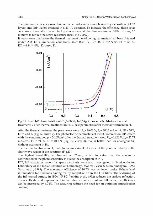
Solar Cells ndash Silicon Wafer-Based Technologies
314
The minimum efficiency was observed when solar cells were obtained by deposition of ITO layers onto InP wafers oriented in (111) A direction To increase the efficiency those solar cells were thermally treated in H2 atmosphere at the temperature of 3500C during 10 minutes to reduce the series resistance (Bruk et al 2007) It was shown that before the thermal treatment the following parameters had been obtained under AM 15 illumination conditions Uoc= 0651 V Isc= 1812 mAcm2 FF = 58 Eff = 684 (Fig 12 curve 1)
-02 00 02 04 06 08
-002
-001
000
001
3
21
J (
Ac
m2)
U (V)
Fig 12 Load I-V characteristics of СunITOpInPAgZn solar cells 1-before thermal treatment 2-after thermal treatment in H2 3-best parameters after thermal treatment in H2
After the thermal treatment the parameters were Uoc= 0658 V Isc= 2013 mAcm2 FF = 58 Eff= 768 (Fig12 curve 2) The photoelectric parameters of the SC received on InP wafers with the concentration p = 31017cm-3 after the thermal treatment were Uoc=0626 V Isc= 2272 mAcm2 FF = 71 Eff= 101 (Fig 12 curve 3) that is better than for analogous SC without treatment in H2 The thermal treatment in H2 leads to the undesirable decrease of the photo sensibility in the short wave region of the spectrum (Fig13) The highest sensibility is observed at 870nm which indicates that the maximum contribution in the photo sensibility is due to the absorption in InP ITOInP structures grown by spray pyrolysis were also investigated in Semiconductor Laboratory of the Indian Institute of Technology Madras (Vasu amp Subrahmanyam 1992 Vasu et al 1993) The maximum efficiency of 107 was achieved under 100mWcm2 illumination for junctions having 5 by weight of tin in the ITO films The texturing of the InP crystal surface in ITOInP SC (Jenkins et al 1992) reduces the surface reflection These cells showed improvement in both short circuit current and fill factor the efficiency can be increased by 674 The texturing reduces the need for an optimum antireflection coating
wwwintechopencom
Solar Cells on the Base of Semiconductor-Insulator-Semiconductor Structures
315
SIS structures for SC fabrication were also obtained on the base of other semiconductor materials besides Si and InP ITOCdTe (Adeeb et al 1987) and ITOGaAs (Simashkevich et al 1992) structures were obtained by spray pyrolysis of ITO layers on pCdTe and pGaAs crystals For ITOCdTe the efficiency was 6 for ITOGaAs SC it did not exceed 25
400 500 600 700 800 900 10000
20
40
60
80
100
120
140
160
180
2
1
I sc (
arb
un
)
(nm) Fig 13 The spectral photo sensibility of Cun+ITOpInPAgZn structure 1- before H2 annealing 2- after H2 annealing
234 Degradation of photoelectric parameters of ITOInP solar cells exposed to ionizing radiation The degradation of photoelectric parameters of ITOInP solar cells after their irradiation by protons with energies Ep=206MeV and flux density up to Fp=1013cm-2 and by electrons with Ec=1MeV and Fele1015cm-2 was investigated (Andronic et al 1998) The results of the photoelectrical parameter measurements at AM0 conditions after the irradiation are presented in Fig 14 Higher efficiency of 116 is obtained if the InP substrate is oriented in [100] plane
Fig 14 The degradation of ITOInP heterostructures photoelectric parameters under protons (a) and (b) electrons irradiation
wwwintechopencom
Solar Cells ndash Silicon Wafer-Based Technologies
316
We notice that after the irradiation of ITOInP solar cells with an integral proton flux of 1013cm-2 their efficiency decreases by 26 that is less than in the case of Si and GaAs based solar cells In the spectral characteristics of ITOpInP solar cells after proton irradiation a small decrease of the photosensitivity in the long wavelength region of the spectrum was observed due to the decrease of the diffusion length Comparing the results of the radiation stability study of ITOInP SC fabricated by spray pyrolysis with the results of similar investigations of other InP based structures it is possible to conclude that in this case the radiation stability is also determined by the low efficiency of radiation defects generation and hence by the low concentration of deep recombination centers reducing the efficiency of solar energy conversion in electric power
3 Fabrication of ITOnSi solar cells with enlarged area by spray pyrolisys
From the brief discussion above it can be concluded that the deposition of ITO layers by spray pyrolysis on the surface of different semiconductor materials allows manufacturing SC through a simple and less expensive technology The most effective are ITOInP SC but because of a very high cost of the InP crystals they cannot be widely used in terrestrial applications To this effect ITOnSi SC with the efficiency higher than 10 may be used but it is necessary to develop the technology for SC fabrication with the active area enlarged up to 70-80 cm2 as is the case of traditional silicon SC with p-n junction
31 Deposition of ITO layers on enlarged silicon wafers ITO layers are deposited on the nSi crystals surface using the specially designed installation (Simashkevich et al 2004 Simashkevich et al 2005) (Fig 15) that has four main units the spraying system (7) the system of displacement and rotation of the support on which the substrate is fixed (4 5) the system of heating the substrate and the system of the evacuation of the residual products of the pyrolysis (8) The heating system consists of an electric furnace (2) and a device for automatic regulation of the substrate temperature with the thermocouple (3) The rest of the installation parts are the power unit (1) the cover (10) and the shielding plate (12) Silicon wafers (11) are located on the support (9) and with the displacement mechanism are moved into the deposition zone of the electric furnace (6) The construction of this mechanism provides the rotation of the support with the velocity of 60 rotations per minute the speed necessary for the obtaining of thin films with uniform thickness on the all wafer surface The alcoholic solution of the mixture SnCl4 + InCl3 is sprayed with compressed oxygen into the stove on the silicon wafer substrate where the ITO thin film is formed due to thermal decomposition of the solution and the oxidation reaction On the heated up substrate there are the chemical reactions describe above in formulas (1) and (2) The BSF nn+ junction was fabricated on the rear side of the wafer by a diffusion process starting from POCl3 gas mixture The junction formation ended with a wet chemical etching of POCl3 residual in a 10 HF bath A junction depth of 1m was chosen in order to minimize recombination To reduce the surface recombination velocity the wafers were thermally oxidized at the temperature of 850oC The main steps of the fabrication of BSC are schematized in Fig 16
32 Properties of ITO layers The properties of the thus obtained ITO films depend on the concentration of indium chloride and tin chloride in the solution the temperature of the substrate the time of
wwwintechopencom
Solar Cells on the Base of Semiconductor-Insulator-Semiconductor Structures
317
spraying and the deposition speed ITO films had a microcrystalline structure that was influenced by the crystal lattice of the support as the X-ray analysis showed They had cubic structure with the lattice constant 1014Aring (Bruk et al 2009)) The SEM image of such an ITO film is presented in Fig 17
(a) (b)
Fig 15 Schematic a) and real b) view of the installation for ITO thin films deposition
ITOSiO2nSi solar cells with the active area of 81cm2 and 486cm2 were fabricated In some cases a BSF region was obtained at the rear contact by phosphor diffusion
Fig 16 SC process sequence
wwwintechopencom
Solar Cells ndash Silicon Wafer-Based Technologies
318
Fig 17 SEM image of ITO film
From Fig 17 it is clear that the ITO film with the thickness of 400nm has a columnar structure the column height being about 300nm and the width 50-100nm ITO films with the maximum conductivity 47middot103 Om-1cm-1 the electron concentration (35divide15)middot1021cm-3 the mobility (15divide30)cm2(Vmiddots) and maximum transmission coefficient in the visible range of the spectrum (87 ) were obtained from solutions containing 90 InCl3 and 10 SnCl4 at the substrate temperature 450degC deposition rate 100 Aringmin spraying time 45 s ITO layers with the thickness 02mm to 07mm and uniform properties on the surface up to 75cm2 were obtained The dependence of the electrical parameters of ITO layers as a function of their composition is given in Table 5
Parameters Ratio of InCl3SnCl4C2H5OH component in the solution
10010 950510 9110 851510 8210 01010 Smiddotcm-1 26middot102 26middot103 47middot103 26middot103 13middot103 424 n cm-3 11middot1020 55middot1020 11middot1021 65middot1020 58middot1020 53middot1019
μ cm-2(Vmiddots) 15 29 27 25 14 5
Table 5 The dependence of the electrical parameters of ITO layers as a function of their composition
The band gap width determined from the spectral dependence of the transmission coefficient is equal to 390eV and changes only for the content of 90-100 of InCl3 in the spraying solution If the content of InCl3 is less than 90 the band gap remains constant and equal to 344eV The optical transmission and reflectance spectra of the deposited on the glass substrate ITO thin films (Simashkevich et al 2004) shows that the transparence in the visible range of spectrum is about 80 20 of the incident radiation is reflected The ITO thin film thickness was varied by changing the quantity of the sprayed solution and it was evaluated from the reflectance spectrum (Simashkevich et al 2004) The thickness of the layer was determined using the relationship (Moss et al 1973)
d=1middot2(2-1)middot2n (4)
where n-refraction index equal to 18 for ITO (Chopra et al 1983) -the wavelengths for two neighboring maximum and minimum d-the thickness of the ITO layer Using this relation the thickness of ITO layers deposited on the nSi wafer surface in dependence on the quantity of the pulverized solution has been determined This relation is linear and the layer thickness varies from 035m up to 05m
wwwintechopencom
Solar Cells on the Base of Semiconductor-Insulator-Semiconductor Structures
319
33 Obtaining of ITOnSi structures The nSi wafers oriented in the (100) plane with resistivity 10 Ohmcm and 45 Ohmcm (concentrations 51015 cm-3 and 11015 cm-3) were used for the fabrication of SIS structures Insulator layers were obtained on the wafers surface by different methods anodic thermal or chemical oxidation The best results have been obtained at the utilization of the two last methods The chemical oxidation of the silicon surface was realized by immersing the silicon wafer into the concentrated nitric acid for 15 seconds A tunnel transparent for minority carriers insulator layers at the ITOSi interface have been obtained thermally if the deposition occurs in an oxygen containing atmosphere Ellipsometrical measurement showed that the thickness of the SiO2 insulator layer varies from 30 Aring to 60 Aring The frontal grid was obtained by Cu vacuum evaporation The investigation of the electrical properties of the obtained SIS structures demonstrates that these insulator layers are tunnel transparent for the current carriers Thereby the obtained ITOnSi SIS structures represent asymmetrical doped barrier structures in which a wide band gap oxide semiconductor plays the role of the transparent metal
4 Physical properties of n+ITOSiO2nSi structures
41 Electric properties Current-voltage characteristics in the temperature range 293Kndash413K were studied The general behavior of the I-V curves of directly biased devices in Fig 18 is characterized by the presence of two straight-line regions with different slopes (Simashkevich et al 2009) Two regions with different behavior could be observed from this figure In the first region at external voltages lower than 03 V the I-V curves are parallel ie the angle of their inclination is constant
00 01 02 03 04 05 06 0710
-7
10-6
10-5
10-4
10-3
10-2
10-1
region 2
Different
slopeI (A
)
U (V)
1-T= 20oC
2-T= 40oC
3-T= 60oC
4-T= 80oC
5-T=100oC
6-T=120oC
7-T=140oC
7 1
region 1
Equal
slope
Fig 18 Temperature dependent direct I-V characteristics in the dark of the n+ITOSiO2nSi solar cells
In this case according to (Riben amp Feucht 1966) the charge carrier transport through the potential barrier is implemented through the tunnel recombination processes in the
wwwintechopencom
Solar Cells ndash Silicon Wafer-Based Technologies
320
space charge region and the current-voltage dependence could be described by the relation
I = Ioexp(AV) exp(BT) (5)
where A and B are constant and do not depend on voltage and temperature respectively The numerical value of the constant A determined from dependences presented in Fig 18 is equal to 15 V-1 The value of the constant B which is equal to 0045 K-1 was calculated from the same dependences that have been re-plotted as lnI = f(T) In (Riben amp Feucht 1966) the constant A is expressed by the relation
A = 8π3hmiddot(me εs SNd)12 (6)
where me ndash is the electron effective mass (in Si in the case considered) εs ndash the dielectric permeability of the silicon and S represents the relative change of the electron energy after each step of the tunneling process Note that 1S represents the number of tunneling steps
(a) (b)
Fig 19 The energy band diagram for a) biases lower than 03 V (the region 1 in Fig 18) b) biases higher than 03 V (region 2 in Fig 18)
The numerical value of A is easily calculated since the other parameters in the respective expression represent fundamental constants or Si physical parameters Hence the mechanism of the charge carrier transport at direct biases of less than 03 V could be interpreted as multi-step tunnel recombination transitions of electrons from the silicon conduction band into the ITO conduction band (see the energy band diagram in Fig19a) the number of steps being about 100 At voltages higher than 03 V (see different slope region in Fig 18) the current flow mechanism through the ITOnSi structure changes The slopes of the I-V curves become temperature dependent that is confirmed by the constant value n about 16 of the parameter n in the relation
I = I0exp(qVankT) (7)
where
I0 = Cexp(-φBkT) (8)
C is a constant depending on the flux current model (emission or diffusion) (Milnes amp Feucht 1972)
wwwintechopencom
Solar Cells on the Base of Semiconductor-Insulator-Semiconductor Structures
321
Such an I-V dependence expressed by relations (7) and (8) is typical for transport mechanisms involving emission of electrons over potential barriers (Fig 19b) Thus at temperatures higher than 20degC an initial voltage that stimulates the electron emission from Si into ITO over the potential barrier at the SiITO interface in n+ITOSiO2nSi structures is of about 03 V From lnI = f (1kT) it is possible to determine the height of the potential barrier φB in ITOnSi structures because the slope of the above-mentioned dependence is equal to φB-qVa The calculated value of φB is 065eV which is in correlation with the experimental data A close value of the height of the potential barrier φB equal to 068 eV was determined also from relation (8) (Simashkevich et al 2009) To sum up in n+ITOSiO2nSi structures two mechanisms of the direct current flow are observed (i) tunneling recombination at direct voltages of less than 03 V and (ii) over barrier emission at voltages higher than 03 V In the former case the direct current flow could be interpreted as multi-step tunnel recombination transitions of electrons from the silicon conduction band into the ITO conduction band the number of steps being of about 100 The reduction of the influence of the former as well as a fine adjustment of the SiO2 thickness in investigated structures will lead to an increased efficiency of converting solar energy into electric energy
42 Photoelectric properties The spectral distribution of the quantum efficiency as well as the photosensitivity of the obtained PV cells have been studied (Simashkevich et al 2004) The monochromatic light from the spectrograph is falling on a semitransparent mirror and is divided into two equal fluxes One flux fall on the surface of a calibrated solar cell for the determination of the incident flux energy and the number (N) of incident photons The second flux falls on the surface of the analyzed sample and the short circuit current Jsc is measured thus permitting the calculation of the number of charge carriers generated by the light and separated by the junction and then the quantum efficiency for each wavelength (Fig 20)
400 600 800 1000 120000
01
02
03
04
05
06
07
08
09
10
00
01
02
03
04
05
06
07
08
09
10
Ph
oto
Sen
siti
vit
y (
AW
)
2
1
Qu
an
tum
Eff
icie
ncy
Wavelength (nm) Fig 20 Spectral distribution of the quantum efficiency (1) and photo sensitivity (2) of the n+ITOSiO2nSi solar cells
wwwintechopencom
Solar Cells ndash Silicon Wafer-Based Technologies
322
The reproducibility of the process and the performances of the devices during samples realization were checked in each batch of samples as well as batch-to-batch The enlargement of the area of the solar cells up to 486cm2 leads to the increasing of the series resistance and to the diminishing of the efficiency down to 7 Thus the method of obtaining n+ITOSiO2nSi structures based on the thin In2O3 Sn layers which are formed on the surface of Si wafers traditionally chemically treated passivated and heated to the temperature of 450degC by spraying chemical solutions of indium tin chloride was elaborated Solar cells based on n+ITOSiO2nSi structures with an active surface up to 486cm2 have been fabricated Maximum efficiency of 1052 is obtained in the case of (100) crystallographic orientation of Si wafer with BSF region at the rear surface and active area of 81 cm2 ITO thickness 03mm SiO2
thickness - 30Aring and the concentration of charge carriers (electrons) in silicon (1-5)times1015cm-3 (Fig 21)
00 01 02 03 04 050
10
20
30
40
Jsc
= 363 mAcm2
Voc
= 0475 V
Rs = 0085 Ohm
Rsh = 6 Ohm
FF = 609
Eff= 1058
Standart conditions
1000Wm2 25
oC AM15
Cu
rren
t d
en
sit
ym
Ac
m2
VoltageV Fig 21 Load I-V characteristic of the n+ITOndashSiO2ndashnSi cells with active area 81cm2 and BSF region at rear surface
The developed technology demonstrates the viability of manufacturing solar cells based on n+ITOSiO2nSi junctions by assembling two 15W and two 30W power solar panels (Fig 22) (Usatii 2011)
5 Bifacial n+SinSiSiO2n
+ITO solar cells
For the first time BSC that are able to convert the solar radiation incident of both sides of the cell into electric power have been produced and investigated fifty years ago (Mori 1960) This type of SC has potential advantages over traditional monofacial SC First there is the possibility of producing more electric power due to the absorption of solar energy by the frontal and rear sides of the device next they do not have a continuous metallic rear contact therefore they are transparent to the infrared radiation which warms
wwwintechopencom
Solar Cells on the Base of Semiconductor-Insulator-Semiconductor Structures
323
the monofacial SC and reduces their efficiency As was presented in (Cuevas 2005) different types of BSC have been fabricated since then but all those BSC are based on p-n junctions fabricated by impurity diffusion in the silicon wafer In case of BSF fabrication these difficulties increase since it is necessary to realize the simultaneous diffusion of different impurities which have an adverse influence on the silicon properties Therefore the problem of protecting the silicon surface from the undesirable impurities appears
(a) (b)
Fig 22 General view of ITOnSi photovoltaic converters a) SC with active aria 486 cm2 b) solar modules with different power
A novel type of BSC formed only by isotype junctions was proposed in (Simashkevich et al 2007) where the possibility was demonstrated to build BSC on the base of nSi crystals and indium tin oxide mixture (ITO) layers obtained by spraying that contain only homopolar junctions with a n+nn+ structure The utilization of such structures removes a considerable part of the above-mentioned problems of BSC fabrication because a single diffusion process is carried out
51 Fabrication and characterization of n+ITOSiO2nn
+Si bifacial solar cells
In the work (Simashkevich et al 2007) the results are presented of producing and investigating the silicon based BSC only on majority carriers The first frontal junction is a SIS structure formed by an ITO layer deposited on the surface of n-type silicon crystal The starting material is an n-type doped (07ndash45Ohmmiddotcm) single crystalline (100) oriented Cz-Silicon 375m thick nSi wafer with the diameter of 4 inches The electron concentrations were 1015cm-3 - 1017 cm-3 An usual BSF structure consisting of a highly doped nSi layer obtained by phosphorus diffusion was fabricated on the topside of the wafer by a diffusion process starting from POCl3 gas mixture The rear nn+ junction formation ends with a wet chemical etching of POCl3 residual in a 10 HF bath A junction depth of 1 m has been chosen in order to minimize recombination To reduce the surface recombination velocity the wafers have been thermally oxidized at a temperature of 850oC Grids obtained by Cu evaporation in vacuum were deposited on the
wwwintechopencom
Solar Cells ndash Silicon Wafer-Based Technologies
324
frontal and back surfaces for BSC fabrication The schematic view of the bifacial ITOnSi solar cell is presented in Fig 23
(a) (b)
Fig 23 The schematic a) and real b) view of the ITOnSi BSC
The spectral distribution of the quantum efficiency of BSC obtained on silicon wafers with different electron concentration has been studied at frontal and back illumination (Fig24) With the frontal illumination in the region of the wavelengths from 400nm to 870nm the value of QY changes in the limits 065ndash095 With the back illumination QY is equal to 06ndash08 in the same region of the spectrum (Bruk et al 2009)
400 500 600 700 800 900 1000 1100 120000
01
02
03
04
05
06
07
08
09
10
QY
arb
un
(nm)
1-(=10Ohmcm)
2-(=45Ohmcm)
3-(=45Ohmcm)
4-(=10Ohmcm)
1
3
2
4
Fig 24 Spectral distribution of the quantum efficiency 1 2-frontal illumination 3 4-rear illumination
wwwintechopencom
Solar Cells on the Base of Semiconductor-Insulator-Semiconductor Structures
325
The I-V load characteristics at AM15 spectral distribution and 1000Wm2 illumination are presented in Fig25
00 01 02 03 040000
0005
0010
0015
0020
0025
0030
0035
Rear illum
Jsc = 1323 mAcm
2
Voc
= 0392 V
FF = 6928
Eff= 360
Frontal illum
Jsc = 3263 mAcm
2
Voc
= 0425 V
FF = 6829
Eff= 947
Cu
rren
t d
ensi
ty
Ac
m2
Voltage V
Fig 25 The I-V load characteristics and the photoelectric parameters of the elaborated BSC at AM15 spectral distribution and 1000Wm2 illumination
The photoelectric parameters of the elaborated BSC have been determined in standard AM15 conditions for the frontal side Voc=0425V Jsc=3263mAcm2 FF=6829 Eff=947 Rser=208Ohm Rsh=67middot103Ohm for the back side Voc=0392V Jsc=1323mAcm2 FF=6928 Eff=36 Rser=340Ohm Rsh=126middot104Ohm The summary efficiency of the BSC is equal to 1307
52 n+ITOSiO2nn
+Si bifacial solar cells with textured surface of Si crystals
Using the method of n+ITOSiO2nn+Si bifacial solar cells fabrication described in (Simashkevich et al 2007) with improved parameters in conformity with p2 of this communication in (Simashkevich et al 2011) two types of bifacial solar cells have been obtained which have different profiles of silicon wafer surface (Fig 26 and Fig 27) It is seen from these data that the effected technology optimization allows to increase of the summary efficiency from 1307 to 1573 in the case of irregular etching of the silicon surface and to 2089 in the case of regular etching The bifaciality ratio also increases from 038 up to 075 On the basis of physical parameters of the silicon wafer ITO layers and of the results of our experiments the energy band diagram of the n+SinSiSiO2n+ITO structure was proposed (Simashkevich et al 2007)
wwwintechopencom
Solar Cells ndash Silicon Wafer-Based Technologies
326
00 01 02 03 04 050
5
10
15
20
25
30
35
Rear illumination
JSC
= 225mAcm2
UOC
= 0461V
FF = 594
Eff = 620
Frontal illumination
JSC
= 346mAcm2
UOC
= 0478V
FF = 574
Eff= 953
Cu
rren
t d
ensi
ty m
Ac
m2
Voltage V
Fig 26 Load I-V characteristic of n+ITOSiO2nn+Si BSC with irregular Si surface
00 01 02 03 04 050
5
10
15
20
25
30
35
Rear illumination
JSC
= 256mAcm2
UOC
= 0458V
FF = 769
Eff= 898
Frontal illumination
JSC
= 343mAcm2
UOC
= 0461V
FF = 750
Eff= 1191
Voltage V
Cu
rren
t d
ensi
ty m
Ac
m2
Fig 27 Load I-V characteristic of n+ITOSiO2nn+Si BSC with regular Si surface
wwwintechopencom
Solar Cells on the Base of Semiconductor-Insulator-Semiconductor Structures
327
Fig 28 Energy band diagram of the bifacial Cun+ITOSiO2nSin+SiCu structure
Fig 28 shows this energy band diagram at illumination in the short-circuit regime At the illumination through the frontal contact the solar radiation is absorbed in the silicon wafer The light generated carriers are separated by the nSiSiO2ITO junction The BSF of the n+SinSi junction facilitate the transport of the carriers to the back contact The same processes take place at the illumination through the rear contact
6 Conclusion
SC fabricated on the basis of semiconductor-insulator- semiconductor structures obtained by deposition of TCO films on the surface of different semiconductor solar materials (Si InP CdTe etc) are promising devices for solar energy conversion due to the simplicity of their fabrication and relatively low cost One of the main advantages of SIS based SC is the elimination of the high temperature diffusion process from the technological chain which is necessary for obtaining p-n junctions the maximum temperature at the SIS structure fabrication being not higher than 450oC The TCO films can be deposited by a variety of techniques among which the spray deposition method is particularly attractive since it is simple relatively fast and vacuum less Between different TCO materials the ITO layers are the most suitable for the fabrication of SIS structures based solar cells Silicon remains the most utilized absorbing semiconductor material for fabrication by spray pyrolysis of such type of SC The maximum efficiency of ITOnSi SC is 10-12 but in the case of textured surface of Si crystals the efficiency reaches more than 15 ITOnSi SC with enlarged area up to 48 cm2 have been obtained by the spray method the efficiency is 1058 for cells with area of 81cm2
wwwintechopencom
Solar Cells ndash Silicon Wafer-Based Technologies
328
InP based SIS structures fabricated by deposition of ITO layers onto pInP crystal surfaces have high efficiencies at the same time they are more simple to fabricate in comparison with diffusion junction cells The efficiency of ITOInP solar cells obtained by spray pyrolisis depends on the crystallographic orientation of the InP wafers The maximum efficiency of 116 was obtained in the case of fabrication of ITOpInPp+InP structures using InP wafers oriented in the (110) plane ITOInP SC obtained by spray pyrolysis demonstrates radiation stability After the irradiation of ITOInP solar cells with an integral proton flux of 1013cm-2 their efficiency decreases by 26 that is less than in the case of Si and GaAs based solar cells A new type of bifacial solar cells n+SinSiSiO2n+ITO based only on isotype junctions was elaborated and fabricated It was demonstrated that the simultaneous illumination of both frontal and rear surfaces of the structures allow to obtain a summary current The technological process of manufacturing such solar cells does not require sophisticated equipment Bifacial solar cells with summary efficiency of 21 and 65 bifaciality coefficient have been obtained using as an absorbent material of single crystalline silicon with a textured surface
7 Acknowledgment
The authors would like to acknowledge Drs EBobeico and VFedorov for carrying out the measurements of some parameters of ITOnSi based solar cells Dr IuUsatii for the help in developing the large-area deposition of ITO layers We thank the direction of the Institute of Applied Physics of the Academy of Sciences of Moldova for support and creation of favorable conditions for investigations We thank Dr Olga Iliasenco for technical assistance We also are grateful to those numerous scientists and engineers worldwide whose data have been included in this overview
8 References
Adeeb N Kretsu I Sherban D Sushkevich C amp Simashkevich A (1987) Spray deposited ITOCdTe solar cells Solar Energy Materials Vol 15 No1 (January 1987) pp9-19 ISSN 0927-0248
Aharoni H Coutts TJ Gessert T Dhere R amp Schilling L (1986) Ion Beam Sputtered Indium Tin Oxide for InP Solar Cells Journal of Vacuum Science and Technology A
VacuumSurfaces and Films Vol 4 No3 pp 428-431 Aharoni H (1999) ITOInP Photovoltaic Devices Proc of the International Solar Energy
Society (ISES) Solar World Congress ISES 1999 SWC Israel ISBN 008 043 8954 Vol 1 pp 95-108 Jerusalem Israel (July 1999)
Anderson RL (1975) Photocurrent suppression in heterojunctions solar cells ApplPhysLett Vol27 No12 (December 1975) pp691-694 ISSN 0003-6951
Andronic I Gagara L Gorceak L Potlog T Sherban D amp Simashkevich A (1998) InP based radiation stable solar cells Proc of the 2nd World Conf on PV Solar Energy
Conversion Vol3 pp3642-3645 ISBN 92-828-5179-6 Vienna (July 1998)
wwwintechopencom
Solar Cells on the Base of Semiconductor-Insulator-Semiconductor Structures
329
Ashok S Sharma PP amp Fonash SJ (1980) Spray-deposited ITOndashSilicon SIS heterojuction solar cells Electron Devices IEEE Transactions on Vol27 No4 725-730 ISSN 0018-9383
Bobeica E Varsano F Roca F amp Parretta A (2001) Light backscattering properties of textured silicon matirials Book of abstracts INFMMeeting ndash National Conferense on the
Physics of Matter pp242-243 Rome Italy (June 2001) Botnariuc VM Gagara LS Gorchac LV Russu EV Simashkevich AV Sherban DA
amp Do Quoc Hung (1990) ITOInP surface barrier solar cells obtained by spray method ApplSolEnergy No3 pp37-40 ISSN 0003-701X
Bruk L Simashkevich A Sherban D Gorceac L Coval A amp Usatii Iu (2007) The
influence of thermal treatment on the parameters of nITOpInP solar cells obtained by pyrolithic spraying method Proc of the 22th European PV Solar Energy Conf pp672-674 ISBN 3-936338-22-1 Milan Italy (September 2007)
Bruk L Fedorov V Sherban D Simashkevicha A Usatii I Bobeico E amp Morvillo P (2009) Isotype bifacial silicon solar cells obtained by ITO spray pyrolysis Materials Science and Engineering B Vol159ndash160 (March 2009) pp282ndash285 ISSN 0921-5107
Calderer J Manifacier JC Szepessy L Darolles JM amp M Perotin (1979) Caracteacuterisation des cellules solaires silicium (n)-In2O3 (dope Sn) preacutepareacutees par une meacutethode de vaporisation Revue de Physique Appliqueacutee Vol14 No3 page 485-490 HAL jpa-00244619 version 1
Chang NS amp Sites R (1978) Electronic characterization of indium tin oxidesilicon photodiodes JApplPhys Vol49 No9 (September 1978) pp4833 -4837 ISSN 0021-8979
Chapin DM Fuller CS amp Pearson GI (1954) A New Silicon p-n Junction Photocell for Converting Solar Radiation into Electrical Power J Appl Phys Vol 25 No5 (May 1954) pp676-677 ISSN 0021-8979
Chopra KL Major S amp Pandya DK (1983) Transparent conductors A status review Thin
Solid Films Vol102 No1 (April 1983) pp1-46 ISSN 0040-6090 Cuevas A (2005) The early history of bifacial solar cells Proc of the 20th European
Photovoltaic Solar Energy Conference pp801-805 ISBN 3-936338-19-1 Barcelona Spain (June 2005)
Dikusar AI Bruk LI Monaico EV Sherban DA Simashkevich AV amp Tiginyanu IM (2008) Photoelectric structures based on nanoporous p-InP Surface
Engineering and Applied Electrochemistry Vol44 No1 (February 2008) pp1-5 ISSN 1068-3755
DuBow J Burk D amp Sites J (1976) Efficient photovoltaic heterojunctions of indium tin oxides on silicon ApplPhysLett Vol29 No8 (October 1976) pp494-496 ISSN 0003-6951
Feng T Ghosh AK amp Fishman C (1979) Efficient electron-beam deposited ITOnSi solar cells JAppl Phys Vol50 No7 (June 1979) pp4972-4974 ISSN 0021-8979
Gagara L Gorcheac L Radu C Radu S Sherban D amp Simaschkevici A (1996) Photovoltaic converters of Solar Energy on the base of SIS structures Proc of the Int
Conf ldquoEuro Sun 96rdquo Vol2 pp665-669 Munchen (August 1996)
wwwintechopencom
Solar Cells ndash Silicon Wafer-Based Technologies
330
Garcia FJ Muci J amp Tomar MS (1982) Preparation of (thin film SnO2)(textured n-Si) solar cells by spray pyrolysis Thin Solid Films Vol97 No1 (November 1982) pp47-51 ISSN 0040-6090
Gessert TA Li X Wanlass MW amp Coutts TJ (1990) Progress in the ITOInP Solar Cell Proc of the second Int Conf rdquoIndium Phosphide and related materialsrdquo pp260-264 Denver CO USA (April 1990)
Gessert TA Li X Coutts TJ Phelps P amp Tsafaras WN (1991) Small-scale production of 4cm2 ITOInP photovoltaic solar cells Proc of the third Int Confrdquo Indium
Phosphide and related materialsrdquo pp32-35 ISBN 0-87942-626-8 Cardiff UK (April 1991)
Horvath ZsJ Subrahmanyam A Manivannan P amp Blasubramanian N (1998) Electrical and photovoltaic study of ITOGaAs and ITOInP heterojunctions Proc of the 2nd
World Conf on PV Solar Energy Conversion Vol3 pp3711-3714 ISBN 92-828-5179-6 Vienna (July 1998)
Jenkins P Landis GA Fatemi N LiX Scheiman D amp Bailey S (1992) Increased efficiency with surface texturing in ITOInP solar cells Proc of the fourth Int Conf ldquoIndium Phosphide and related materialsrdquo pp186-189 ISBN 0-87942-626-8 Newport RI USA (April 1992)
Kobayashi H IshidaT Nakato Y amp Tsubomura H (1991) Mechanism of carrier transport in highly efficient solar sells having indium tin oxideSi junction JApplPhys Vol69 No3 (February 1991) pp1736-1743 ISSN 0021-8979
Li X Wanlass MW Gessert TA Emery KA amp Coutts TJ (1989) High-efficiency indium tin oxideindium phosphide solar cells Appl Phys Lett Vol54 No26 (June 1989) pp2674-2676 ISSN 0003-6951
Malik A Baranyuk V amp Manasson V (1979) Solar cells based on the SnO2-SiO2-Si heterojunction ApplSolEnergy No2 pp83-84 ISSN 0003-701X
Malik A Baranyuk V amp Manasson V (1980) Improved model of solar cells based on the In2O3SnO2SiO2nSi structure Appl Sol Energy No1 pp1-2 ISSN 0003-701X
Malik O De la Hidalga-W FJ Zuniga ndashI C amp Ruiz-T G (2008) Efficient ITOSi solar cells fabricatd with a low temperature technology Results and perspectives Journal of Non -Crystalline Solids Vol354 No19-25 pp2472-2477 ISSN 0022-3093
Malik O amp FJavier De La Hidalga-W (2009) Efficient Silicon Solar Cells Fabricated with a Low Cost Spray Technique In Solar Energy Radu D Rugescu pp (81-104) In theh ISBN 978-953-307-052-0 Vukovar Croatia
Manifacier JC amp Szepessy L (1977) Efficient sprayed In2O3Sn n-type silicon heterojunction solar cell Appl Phys Lett Vol31 No7 (October 1977) pp459-462 ISSN 0003-6951
Marques F amp Chambouleyron I (1986) Surface barrier SnO2SiOxcSi(n) solar cells optimization of the fabrication process Solar Cells Vol17 No2-3 (April-May 1986) pp167-181 ISSN 0927-0248
Milnes AG amp Feucht DL (1972) Heterojunctions and metal-semiconductor junctions Academic Press Inc (October 1972) ISBN-10 0124980503 ISBN-13 978-0124980501 New-York and London 408 p
wwwintechopencom
Solar Cells on the Base of Semiconductor-Insulator-Semiconductor Structures
331
Mizrah T amp Adler D (1976) Operation of ITO-Si heterojunction solar cells ApplPhysLett Vol29 No8 (November 1976) pp682-684 ISSN 0003-6951
Moss TS Burrell GJ amp Ellis B (1973) Semiconductor Opto-Electronics Butterworths London
Nagatomo T Endo M amp Omoto O (1979) Fabrication and characterization of SnO2n-Si solar cells Jpn J Appl Phys Vol18 No6 (June 1979) pp1103-1109 ISSN 0021-4922
Nagatomo T Inagaki Y Amano Y amp Omoto O (1982) A comparison of spray deposited ITOn-Si and SnO2n-Si solar cells Jpn J Appl Phys Vol21 Suppl21-2 pp121-124 ISSN 0021-4922
Riben AR amp Feucht DL (1966) Electrical transport in nGe-pGaAs heterojunctions International Journal of Electronics Vol20 No6 (June 1966) pp583-599 ISSN 0020-7217
Saim HB amp Campbell DS (1987) Properties of indium-tin-oxide (ITO)silicon heterojunction solar cells by thick-film techniques Solar Energy Materials Vol15 No4 (May-June 1987) pp 249-260 ISSN 0927-0248
Shewchun J Dubow G Myszhkowsky A amp Singh R (1978) The operation of semiconductor-insulator-semiconductor (SIS) solar cells Theory J Appl Phys Vol49 No2 (February 1978) pp855-864 ISSN 0022-3727
Shewchun J Burk D Singh R Spitzer M amp Dubow G (1979) The semiconductor-insulator-semiconductor (indium tin oxide on silicon) solar cells characteristics and loss mechanisms JApplPhys Vol50 No10 (October 1979) pp6524-6533 ISSN 0021-8979
Shewchun J Dubow G Wilmsen C Singh R Burk D amp Wagner J (1979) The operation of semiconductor-insulator-semiconductor (SIS) solar cells Experiment JApplPhys Vol50 No4 (April 1979) pp2832-2839 ISSN 0021-8979
Shewchun J Burc D amp Spitzer MB (1980) MIS and SIS solar cells Electron Devices IEEE
Transactions on Vol27 No4 pp705-716 ISSN 0018-9383 Simashkevich A Toyi J-M Sherban D amp Yakubu H (1992) Investigation of ITO-GaAs
structures Bull of ASM Physamp Tech No3 pp26-29 Simashkevich A Do Quoc Hung Bobeico E Gorcheac L amp Sherban D (1999) Solar cells
based on SIS structures Proc of the 3rd Int Workshop on Material Science Part1 pp56-59 ISBN 90-5776-033-9 Hanoi Vietnam (November 1999)
Simashkevich A Sherban D Bruc L Coval A Fedorov V Bobeico E amp Usatii Iu (2004) I Spray-deposited ITOnSi solar cells with enlarged area Moldavian
Journal of Physical Sciences Vol3 No3-4 (December 2004) pp334-339 ISSN 1810-648X
Simashkevich A Serban D Bruc L Coval A Fedorov V Bobeico E amp Usatii Iu (2005) Spray deposited ITOnSi solar cells with enlarged area Proc of the 20th
European Photovoltaic Solar Energy Conference pp980-982 ISBN 3-936338-19-1 Barcelona Spain (June 2005)
wwwintechopencom
Solar Cells ndash Silicon Wafer-Based Technologies
332
Simashkevich A Sherban D Morvillo P Bobeico E Bruk L amp Usatii Iu (2007) Bifacial solar cells based on isotype junctions Proc of the 22th European PV Solar Energy
Conf ISBN 3-936338-22-1 Milan Italy (September 2007) pp484-486 Simashkevich A Sherban D Rusu M Bruk L amp Usatii Iu (2009) ITOnSi solar cells
voltage dependent charge transport mechanisms Proc of the 24th European
Photovoltaic Solar Energy Conference pp2230-2232 ISBN 3-936338-24-1 Hamburg Germany (September 2009)
Simashkevich A Serban D Bruc L Fyodorov V Coval A amp Usatii Iu (2010) Features of the mechanism of a current flowing through an ITOnSi isotype structure Surface engineering and applied electrochemistry Vol46 No1 (February 2010) pp40-42 ISSN 1068-3755
Simashkevich AV Sherban DA Bruk LI Usatii IuV amp Fedorov VM (2010) Transparent Conductive Oxide Layers and Their Application in Solar Energetic Physics and Chemistry of Solid State Vol11 No4 (October 2010) pp 950-956
Simashkevich AV Sherban DA Bruk LI Harea EE amp Usatii Iu (2011) Efficient ITOnSi solar cells with silicon textured surface Elektronnaya Obrabotka Materialov Vol47 No3 ( May-June 2011) pp79-84 ISSN 0013-5739
Tarr N amp Pulfrey D (1979) New experimental evidence for minority-carrier Appl Phys
Lett V34 No4 (February 1979) pp295-297 ISSN 0003-6951 Untila GG Chebotareva AV Osipov AS amp Samborsky DV (1998) Series resistance of
solar cell with antireflection coating of transparent conducting oxide Proc of the 2nd
World Conf on PV Solar Energy Conversion Vol1 pp300-302 ISBN 92-828-5179-6 Vienna (July 1998)
Usatii Iu (2011) Preparation of ITO-Si solar cells with enlarged area and the study of their properties (in Romanian) PhD Thesis Chisinau (February 2011)
Vasu V amp Aubrahmanyam A (1992) Photovoltaic properties of indium tin oxide (ITO)silicon junctions prepared by spray pyrolysis - dependence on oxidation time Semicond Sci and Tech Vol7 No3 (March 1992) pp320-323 ISSN 0268-1242
Vasu V Subrahmanyam A Kumar J amp Ramasamy P (1993) Spray-pyrolytic-grown ITOInP junctions effect of tin doping Semicond Sci Technol Vol8 No3 (March 1993) pp437-440 ISSN 0268-1242
Wishwakarma S Rahmatullah R amp Prasad HC (1993) Low cost SnO2PSiO2n-Si (textured) heterojunction solar cells JPhysDApplPhys v26 No6 (June 1993) pp959-962 ISSN 0022-3727
Yamamoto A Yamaguchi M amp Uemura C (1984) High conversion efficiency and high radiation resistance InP homojunction solar cells Appl Phys Lett Vol44 No6 (March 1984) pp611-614 ISSN 0003-6951
wwwintechopencom
Solar Cells - Silicon Wafer-Based TechnologiesEdited by Prof Leonid A Kosyachenko
ISBN 978-953-307-747-5Hard cover 364 pagesPublisher InTechPublished online 02 November 2011Published in print edition November 2011
InTech EuropeUniversity Campus STeP Ri Slavka Krautzeka 83A 51000 Rijeka Croatia Phone +385 (51) 770 447 Fax +385 (51) 686 166wwwintechopencom
InTech ChinaUnit 405 Office Block Hotel Equatorial Shanghai No65 Yan An Road (West) Shanghai 200040 China
Phone +86-21-62489820 Fax +86-21-62489821
The third book of four-volume edition of Solar Cells is devoted to solar cells based on silicon wafers ie themain material used in todays photovoltaics The volume includes the chapters that present new results ofresearch aimed to improve efficiency to reduce consumption of materials and to lower cost of wafer-basedsilicon solar cells as well as new methods of research and testing of the devices Light trapping design in c-Siand mc-Si solar cells solar-energy conversion as a function of the geometric-concentration factor designcriteria for spacecraft solar arrays are considered in several chapters A system for the micrometriccharacterization of solar cells for identifying the electrical parameters of PV solar generators a new model forextracting the physical parameters of solar cells LBIC method for characterization of solar cells non-idealitiesin the I-V characteristic of the PV generators are discussed in other chapters of the volume
How to referenceIn order to correctly reference this scholarly work feel free to copy and paste the following
Alexei Simaschevici Dormidont Serban and Leonid Bruc (2011) Solar Cells on the Base of Semiconductor-Insulator-Semiconductor Structures Solar Cells - Silicon Wafer-Based Technologies Prof Leonid AKosyachenko (Ed) ISBN 978-953-307-747-5 InTech Available fromhttpwwwintechopencombookssolar-cells-silicon-wafer-based-technologiessolar-cells-on-the-base-of-semiconductor-insulator-semiconductor-structures
copy 2011 The Author(s) Licensee IntechOpen This is an open access articledistributed under the terms of the Creative Commons Attribution 30License which permits unrestricted use distribution and reproduction inany medium provided the original work is properly cited

Solar Cells on the Base of Semiconductor-Insulator-Semiconductor Structures
315
SIS structures for SC fabrication were also obtained on the base of other semiconductor materials besides Si and InP ITOCdTe (Adeeb et al 1987) and ITOGaAs (Simashkevich et al 1992) structures were obtained by spray pyrolysis of ITO layers on pCdTe and pGaAs crystals For ITOCdTe the efficiency was 6 for ITOGaAs SC it did not exceed 25
400 500 600 700 800 900 10000
20
40
60
80
100
120
140
160
180
2
1
I sc (
arb
un
)
(nm) Fig 13 The spectral photo sensibility of Cun+ITOpInPAgZn structure 1- before H2 annealing 2- after H2 annealing
234 Degradation of photoelectric parameters of ITOInP solar cells exposed to ionizing radiation The degradation of photoelectric parameters of ITOInP solar cells after their irradiation by protons with energies Ep=206MeV and flux density up to Fp=1013cm-2 and by electrons with Ec=1MeV and Fele1015cm-2 was investigated (Andronic et al 1998) The results of the photoelectrical parameter measurements at AM0 conditions after the irradiation are presented in Fig 14 Higher efficiency of 116 is obtained if the InP substrate is oriented in [100] plane
Fig 14 The degradation of ITOInP heterostructures photoelectric parameters under protons (a) and (b) electrons irradiation
wwwintechopencom
Solar Cells ndash Silicon Wafer-Based Technologies
316
We notice that after the irradiation of ITOInP solar cells with an integral proton flux of 1013cm-2 their efficiency decreases by 26 that is less than in the case of Si and GaAs based solar cells In the spectral characteristics of ITOpInP solar cells after proton irradiation a small decrease of the photosensitivity in the long wavelength region of the spectrum was observed due to the decrease of the diffusion length Comparing the results of the radiation stability study of ITOInP SC fabricated by spray pyrolysis with the results of similar investigations of other InP based structures it is possible to conclude that in this case the radiation stability is also determined by the low efficiency of radiation defects generation and hence by the low concentration of deep recombination centers reducing the efficiency of solar energy conversion in electric power
3 Fabrication of ITOnSi solar cells with enlarged area by spray pyrolisys
From the brief discussion above it can be concluded that the deposition of ITO layers by spray pyrolysis on the surface of different semiconductor materials allows manufacturing SC through a simple and less expensive technology The most effective are ITOInP SC but because of a very high cost of the InP crystals they cannot be widely used in terrestrial applications To this effect ITOnSi SC with the efficiency higher than 10 may be used but it is necessary to develop the technology for SC fabrication with the active area enlarged up to 70-80 cm2 as is the case of traditional silicon SC with p-n junction
31 Deposition of ITO layers on enlarged silicon wafers ITO layers are deposited on the nSi crystals surface using the specially designed installation (Simashkevich et al 2004 Simashkevich et al 2005) (Fig 15) that has four main units the spraying system (7) the system of displacement and rotation of the support on which the substrate is fixed (4 5) the system of heating the substrate and the system of the evacuation of the residual products of the pyrolysis (8) The heating system consists of an electric furnace (2) and a device for automatic regulation of the substrate temperature with the thermocouple (3) The rest of the installation parts are the power unit (1) the cover (10) and the shielding plate (12) Silicon wafers (11) are located on the support (9) and with the displacement mechanism are moved into the deposition zone of the electric furnace (6) The construction of this mechanism provides the rotation of the support with the velocity of 60 rotations per minute the speed necessary for the obtaining of thin films with uniform thickness on the all wafer surface The alcoholic solution of the mixture SnCl4 + InCl3 is sprayed with compressed oxygen into the stove on the silicon wafer substrate where the ITO thin film is formed due to thermal decomposition of the solution and the oxidation reaction On the heated up substrate there are the chemical reactions describe above in formulas (1) and (2) The BSF nn+ junction was fabricated on the rear side of the wafer by a diffusion process starting from POCl3 gas mixture The junction formation ended with a wet chemical etching of POCl3 residual in a 10 HF bath A junction depth of 1m was chosen in order to minimize recombination To reduce the surface recombination velocity the wafers were thermally oxidized at the temperature of 850oC The main steps of the fabrication of BSC are schematized in Fig 16
32 Properties of ITO layers The properties of the thus obtained ITO films depend on the concentration of indium chloride and tin chloride in the solution the temperature of the substrate the time of
wwwintechopencom
Solar Cells on the Base of Semiconductor-Insulator-Semiconductor Structures
317
spraying and the deposition speed ITO films had a microcrystalline structure that was influenced by the crystal lattice of the support as the X-ray analysis showed They had cubic structure with the lattice constant 1014Aring (Bruk et al 2009)) The SEM image of such an ITO film is presented in Fig 17
(a) (b)
Fig 15 Schematic a) and real b) view of the installation for ITO thin films deposition
ITOSiO2nSi solar cells with the active area of 81cm2 and 486cm2 were fabricated In some cases a BSF region was obtained at the rear contact by phosphor diffusion
Fig 16 SC process sequence
wwwintechopencom
Solar Cells ndash Silicon Wafer-Based Technologies
318
Fig 17 SEM image of ITO film
From Fig 17 it is clear that the ITO film with the thickness of 400nm has a columnar structure the column height being about 300nm and the width 50-100nm ITO films with the maximum conductivity 47middot103 Om-1cm-1 the electron concentration (35divide15)middot1021cm-3 the mobility (15divide30)cm2(Vmiddots) and maximum transmission coefficient in the visible range of the spectrum (87 ) were obtained from solutions containing 90 InCl3 and 10 SnCl4 at the substrate temperature 450degC deposition rate 100 Aringmin spraying time 45 s ITO layers with the thickness 02mm to 07mm and uniform properties on the surface up to 75cm2 were obtained The dependence of the electrical parameters of ITO layers as a function of their composition is given in Table 5
Parameters Ratio of InCl3SnCl4C2H5OH component in the solution
10010 950510 9110 851510 8210 01010 Smiddotcm-1 26middot102 26middot103 47middot103 26middot103 13middot103 424 n cm-3 11middot1020 55middot1020 11middot1021 65middot1020 58middot1020 53middot1019
μ cm-2(Vmiddots) 15 29 27 25 14 5
Table 5 The dependence of the electrical parameters of ITO layers as a function of their composition
The band gap width determined from the spectral dependence of the transmission coefficient is equal to 390eV and changes only for the content of 90-100 of InCl3 in the spraying solution If the content of InCl3 is less than 90 the band gap remains constant and equal to 344eV The optical transmission and reflectance spectra of the deposited on the glass substrate ITO thin films (Simashkevich et al 2004) shows that the transparence in the visible range of spectrum is about 80 20 of the incident radiation is reflected The ITO thin film thickness was varied by changing the quantity of the sprayed solution and it was evaluated from the reflectance spectrum (Simashkevich et al 2004) The thickness of the layer was determined using the relationship (Moss et al 1973)
d=1middot2(2-1)middot2n (4)
where n-refraction index equal to 18 for ITO (Chopra et al 1983) -the wavelengths for two neighboring maximum and minimum d-the thickness of the ITO layer Using this relation the thickness of ITO layers deposited on the nSi wafer surface in dependence on the quantity of the pulverized solution has been determined This relation is linear and the layer thickness varies from 035m up to 05m
wwwintechopencom
Solar Cells on the Base of Semiconductor-Insulator-Semiconductor Structures
319
33 Obtaining of ITOnSi structures The nSi wafers oriented in the (100) plane with resistivity 10 Ohmcm and 45 Ohmcm (concentrations 51015 cm-3 and 11015 cm-3) were used for the fabrication of SIS structures Insulator layers were obtained on the wafers surface by different methods anodic thermal or chemical oxidation The best results have been obtained at the utilization of the two last methods The chemical oxidation of the silicon surface was realized by immersing the silicon wafer into the concentrated nitric acid for 15 seconds A tunnel transparent for minority carriers insulator layers at the ITOSi interface have been obtained thermally if the deposition occurs in an oxygen containing atmosphere Ellipsometrical measurement showed that the thickness of the SiO2 insulator layer varies from 30 Aring to 60 Aring The frontal grid was obtained by Cu vacuum evaporation The investigation of the electrical properties of the obtained SIS structures demonstrates that these insulator layers are tunnel transparent for the current carriers Thereby the obtained ITOnSi SIS structures represent asymmetrical doped barrier structures in which a wide band gap oxide semiconductor plays the role of the transparent metal
4 Physical properties of n+ITOSiO2nSi structures
41 Electric properties Current-voltage characteristics in the temperature range 293Kndash413K were studied The general behavior of the I-V curves of directly biased devices in Fig 18 is characterized by the presence of two straight-line regions with different slopes (Simashkevich et al 2009) Two regions with different behavior could be observed from this figure In the first region at external voltages lower than 03 V the I-V curves are parallel ie the angle of their inclination is constant
00 01 02 03 04 05 06 0710
-7
10-6
10-5
10-4
10-3
10-2
10-1
region 2
Different
slopeI (A
)
U (V)
1-T= 20oC
2-T= 40oC
3-T= 60oC
4-T= 80oC
5-T=100oC
6-T=120oC
7-T=140oC
7 1
region 1
Equal
slope
Fig 18 Temperature dependent direct I-V characteristics in the dark of the n+ITOSiO2nSi solar cells
In this case according to (Riben amp Feucht 1966) the charge carrier transport through the potential barrier is implemented through the tunnel recombination processes in the
wwwintechopencom
Solar Cells ndash Silicon Wafer-Based Technologies
320
space charge region and the current-voltage dependence could be described by the relation
I = Ioexp(AV) exp(BT) (5)
where A and B are constant and do not depend on voltage and temperature respectively The numerical value of the constant A determined from dependences presented in Fig 18 is equal to 15 V-1 The value of the constant B which is equal to 0045 K-1 was calculated from the same dependences that have been re-plotted as lnI = f(T) In (Riben amp Feucht 1966) the constant A is expressed by the relation
A = 8π3hmiddot(me εs SNd)12 (6)
where me ndash is the electron effective mass (in Si in the case considered) εs ndash the dielectric permeability of the silicon and S represents the relative change of the electron energy after each step of the tunneling process Note that 1S represents the number of tunneling steps
(a) (b)
Fig 19 The energy band diagram for a) biases lower than 03 V (the region 1 in Fig 18) b) biases higher than 03 V (region 2 in Fig 18)
The numerical value of A is easily calculated since the other parameters in the respective expression represent fundamental constants or Si physical parameters Hence the mechanism of the charge carrier transport at direct biases of less than 03 V could be interpreted as multi-step tunnel recombination transitions of electrons from the silicon conduction band into the ITO conduction band (see the energy band diagram in Fig19a) the number of steps being about 100 At voltages higher than 03 V (see different slope region in Fig 18) the current flow mechanism through the ITOnSi structure changes The slopes of the I-V curves become temperature dependent that is confirmed by the constant value n about 16 of the parameter n in the relation
I = I0exp(qVankT) (7)
where
I0 = Cexp(-φBkT) (8)
C is a constant depending on the flux current model (emission or diffusion) (Milnes amp Feucht 1972)
wwwintechopencom
Solar Cells on the Base of Semiconductor-Insulator-Semiconductor Structures
321
Such an I-V dependence expressed by relations (7) and (8) is typical for transport mechanisms involving emission of electrons over potential barriers (Fig 19b) Thus at temperatures higher than 20degC an initial voltage that stimulates the electron emission from Si into ITO over the potential barrier at the SiITO interface in n+ITOSiO2nSi structures is of about 03 V From lnI = f (1kT) it is possible to determine the height of the potential barrier φB in ITOnSi structures because the slope of the above-mentioned dependence is equal to φB-qVa The calculated value of φB is 065eV which is in correlation with the experimental data A close value of the height of the potential barrier φB equal to 068 eV was determined also from relation (8) (Simashkevich et al 2009) To sum up in n+ITOSiO2nSi structures two mechanisms of the direct current flow are observed (i) tunneling recombination at direct voltages of less than 03 V and (ii) over barrier emission at voltages higher than 03 V In the former case the direct current flow could be interpreted as multi-step tunnel recombination transitions of electrons from the silicon conduction band into the ITO conduction band the number of steps being of about 100 The reduction of the influence of the former as well as a fine adjustment of the SiO2 thickness in investigated structures will lead to an increased efficiency of converting solar energy into electric energy
42 Photoelectric properties The spectral distribution of the quantum efficiency as well as the photosensitivity of the obtained PV cells have been studied (Simashkevich et al 2004) The monochromatic light from the spectrograph is falling on a semitransparent mirror and is divided into two equal fluxes One flux fall on the surface of a calibrated solar cell for the determination of the incident flux energy and the number (N) of incident photons The second flux falls on the surface of the analyzed sample and the short circuit current Jsc is measured thus permitting the calculation of the number of charge carriers generated by the light and separated by the junction and then the quantum efficiency for each wavelength (Fig 20)
400 600 800 1000 120000
01
02
03
04
05
06
07
08
09
10
00
01
02
03
04
05
06
07
08
09
10
Ph
oto
Sen
siti
vit
y (
AW
)
2
1
Qu
an
tum
Eff
icie
ncy
Wavelength (nm) Fig 20 Spectral distribution of the quantum efficiency (1) and photo sensitivity (2) of the n+ITOSiO2nSi solar cells
wwwintechopencom
Solar Cells ndash Silicon Wafer-Based Technologies
322
The reproducibility of the process and the performances of the devices during samples realization were checked in each batch of samples as well as batch-to-batch The enlargement of the area of the solar cells up to 486cm2 leads to the increasing of the series resistance and to the diminishing of the efficiency down to 7 Thus the method of obtaining n+ITOSiO2nSi structures based on the thin In2O3 Sn layers which are formed on the surface of Si wafers traditionally chemically treated passivated and heated to the temperature of 450degC by spraying chemical solutions of indium tin chloride was elaborated Solar cells based on n+ITOSiO2nSi structures with an active surface up to 486cm2 have been fabricated Maximum efficiency of 1052 is obtained in the case of (100) crystallographic orientation of Si wafer with BSF region at the rear surface and active area of 81 cm2 ITO thickness 03mm SiO2
thickness - 30Aring and the concentration of charge carriers (electrons) in silicon (1-5)times1015cm-3 (Fig 21)
00 01 02 03 04 050
10
20
30
40
Jsc
= 363 mAcm2
Voc
= 0475 V
Rs = 0085 Ohm
Rsh = 6 Ohm
FF = 609
Eff= 1058
Standart conditions
1000Wm2 25
oC AM15
Cu
rren
t d
en
sit
ym
Ac
m2
VoltageV Fig 21 Load I-V characteristic of the n+ITOndashSiO2ndashnSi cells with active area 81cm2 and BSF region at rear surface
The developed technology demonstrates the viability of manufacturing solar cells based on n+ITOSiO2nSi junctions by assembling two 15W and two 30W power solar panels (Fig 22) (Usatii 2011)
5 Bifacial n+SinSiSiO2n
+ITO solar cells
For the first time BSC that are able to convert the solar radiation incident of both sides of the cell into electric power have been produced and investigated fifty years ago (Mori 1960) This type of SC has potential advantages over traditional monofacial SC First there is the possibility of producing more electric power due to the absorption of solar energy by the frontal and rear sides of the device next they do not have a continuous metallic rear contact therefore they are transparent to the infrared radiation which warms
wwwintechopencom
Solar Cells on the Base of Semiconductor-Insulator-Semiconductor Structures
323
the monofacial SC and reduces their efficiency As was presented in (Cuevas 2005) different types of BSC have been fabricated since then but all those BSC are based on p-n junctions fabricated by impurity diffusion in the silicon wafer In case of BSF fabrication these difficulties increase since it is necessary to realize the simultaneous diffusion of different impurities which have an adverse influence on the silicon properties Therefore the problem of protecting the silicon surface from the undesirable impurities appears
(a) (b)
Fig 22 General view of ITOnSi photovoltaic converters a) SC with active aria 486 cm2 b) solar modules with different power
A novel type of BSC formed only by isotype junctions was proposed in (Simashkevich et al 2007) where the possibility was demonstrated to build BSC on the base of nSi crystals and indium tin oxide mixture (ITO) layers obtained by spraying that contain only homopolar junctions with a n+nn+ structure The utilization of such structures removes a considerable part of the above-mentioned problems of BSC fabrication because a single diffusion process is carried out
51 Fabrication and characterization of n+ITOSiO2nn
+Si bifacial solar cells
In the work (Simashkevich et al 2007) the results are presented of producing and investigating the silicon based BSC only on majority carriers The first frontal junction is a SIS structure formed by an ITO layer deposited on the surface of n-type silicon crystal The starting material is an n-type doped (07ndash45Ohmmiddotcm) single crystalline (100) oriented Cz-Silicon 375m thick nSi wafer with the diameter of 4 inches The electron concentrations were 1015cm-3 - 1017 cm-3 An usual BSF structure consisting of a highly doped nSi layer obtained by phosphorus diffusion was fabricated on the topside of the wafer by a diffusion process starting from POCl3 gas mixture The rear nn+ junction formation ends with a wet chemical etching of POCl3 residual in a 10 HF bath A junction depth of 1 m has been chosen in order to minimize recombination To reduce the surface recombination velocity the wafers have been thermally oxidized at a temperature of 850oC Grids obtained by Cu evaporation in vacuum were deposited on the
wwwintechopencom
Solar Cells ndash Silicon Wafer-Based Technologies
324
frontal and back surfaces for BSC fabrication The schematic view of the bifacial ITOnSi solar cell is presented in Fig 23
(a) (b)
Fig 23 The schematic a) and real b) view of the ITOnSi BSC
The spectral distribution of the quantum efficiency of BSC obtained on silicon wafers with different electron concentration has been studied at frontal and back illumination (Fig24) With the frontal illumination in the region of the wavelengths from 400nm to 870nm the value of QY changes in the limits 065ndash095 With the back illumination QY is equal to 06ndash08 in the same region of the spectrum (Bruk et al 2009)
400 500 600 700 800 900 1000 1100 120000
01
02
03
04
05
06
07
08
09
10
QY
arb
un
(nm)
1-(=10Ohmcm)
2-(=45Ohmcm)
3-(=45Ohmcm)
4-(=10Ohmcm)
1
3
2
4
Fig 24 Spectral distribution of the quantum efficiency 1 2-frontal illumination 3 4-rear illumination
wwwintechopencom
Solar Cells on the Base of Semiconductor-Insulator-Semiconductor Structures
325
The I-V load characteristics at AM15 spectral distribution and 1000Wm2 illumination are presented in Fig25
00 01 02 03 040000
0005
0010
0015
0020
0025
0030
0035
Rear illum
Jsc = 1323 mAcm
2
Voc
= 0392 V
FF = 6928
Eff= 360
Frontal illum
Jsc = 3263 mAcm
2
Voc
= 0425 V
FF = 6829
Eff= 947
Cu
rren
t d
ensi
ty
Ac
m2
Voltage V
Fig 25 The I-V load characteristics and the photoelectric parameters of the elaborated BSC at AM15 spectral distribution and 1000Wm2 illumination
The photoelectric parameters of the elaborated BSC have been determined in standard AM15 conditions for the frontal side Voc=0425V Jsc=3263mAcm2 FF=6829 Eff=947 Rser=208Ohm Rsh=67middot103Ohm for the back side Voc=0392V Jsc=1323mAcm2 FF=6928 Eff=36 Rser=340Ohm Rsh=126middot104Ohm The summary efficiency of the BSC is equal to 1307
52 n+ITOSiO2nn
+Si bifacial solar cells with textured surface of Si crystals
Using the method of n+ITOSiO2nn+Si bifacial solar cells fabrication described in (Simashkevich et al 2007) with improved parameters in conformity with p2 of this communication in (Simashkevich et al 2011) two types of bifacial solar cells have been obtained which have different profiles of silicon wafer surface (Fig 26 and Fig 27) It is seen from these data that the effected technology optimization allows to increase of the summary efficiency from 1307 to 1573 in the case of irregular etching of the silicon surface and to 2089 in the case of regular etching The bifaciality ratio also increases from 038 up to 075 On the basis of physical parameters of the silicon wafer ITO layers and of the results of our experiments the energy band diagram of the n+SinSiSiO2n+ITO structure was proposed (Simashkevich et al 2007)
wwwintechopencom
Solar Cells ndash Silicon Wafer-Based Technologies
326
00 01 02 03 04 050
5
10
15
20
25
30
35
Rear illumination
JSC
= 225mAcm2
UOC
= 0461V
FF = 594
Eff = 620
Frontal illumination
JSC
= 346mAcm2
UOC
= 0478V
FF = 574
Eff= 953
Cu
rren
t d
ensi
ty m
Ac
m2
Voltage V
Fig 26 Load I-V characteristic of n+ITOSiO2nn+Si BSC with irregular Si surface
00 01 02 03 04 050
5
10
15
20
25
30
35
Rear illumination
JSC
= 256mAcm2
UOC
= 0458V
FF = 769
Eff= 898
Frontal illumination
JSC
= 343mAcm2
UOC
= 0461V
FF = 750
Eff= 1191
Voltage V
Cu
rren
t d
ensi
ty m
Ac
m2
Fig 27 Load I-V characteristic of n+ITOSiO2nn+Si BSC with regular Si surface
wwwintechopencom
Solar Cells on the Base of Semiconductor-Insulator-Semiconductor Structures
327
Fig 28 Energy band diagram of the bifacial Cun+ITOSiO2nSin+SiCu structure
Fig 28 shows this energy band diagram at illumination in the short-circuit regime At the illumination through the frontal contact the solar radiation is absorbed in the silicon wafer The light generated carriers are separated by the nSiSiO2ITO junction The BSF of the n+SinSi junction facilitate the transport of the carriers to the back contact The same processes take place at the illumination through the rear contact
6 Conclusion
SC fabricated on the basis of semiconductor-insulator- semiconductor structures obtained by deposition of TCO films on the surface of different semiconductor solar materials (Si InP CdTe etc) are promising devices for solar energy conversion due to the simplicity of their fabrication and relatively low cost One of the main advantages of SIS based SC is the elimination of the high temperature diffusion process from the technological chain which is necessary for obtaining p-n junctions the maximum temperature at the SIS structure fabrication being not higher than 450oC The TCO films can be deposited by a variety of techniques among which the spray deposition method is particularly attractive since it is simple relatively fast and vacuum less Between different TCO materials the ITO layers are the most suitable for the fabrication of SIS structures based solar cells Silicon remains the most utilized absorbing semiconductor material for fabrication by spray pyrolysis of such type of SC The maximum efficiency of ITOnSi SC is 10-12 but in the case of textured surface of Si crystals the efficiency reaches more than 15 ITOnSi SC with enlarged area up to 48 cm2 have been obtained by the spray method the efficiency is 1058 for cells with area of 81cm2
wwwintechopencom
Solar Cells ndash Silicon Wafer-Based Technologies
328
InP based SIS structures fabricated by deposition of ITO layers onto pInP crystal surfaces have high efficiencies at the same time they are more simple to fabricate in comparison with diffusion junction cells The efficiency of ITOInP solar cells obtained by spray pyrolisis depends on the crystallographic orientation of the InP wafers The maximum efficiency of 116 was obtained in the case of fabrication of ITOpInPp+InP structures using InP wafers oriented in the (110) plane ITOInP SC obtained by spray pyrolysis demonstrates radiation stability After the irradiation of ITOInP solar cells with an integral proton flux of 1013cm-2 their efficiency decreases by 26 that is less than in the case of Si and GaAs based solar cells A new type of bifacial solar cells n+SinSiSiO2n+ITO based only on isotype junctions was elaborated and fabricated It was demonstrated that the simultaneous illumination of both frontal and rear surfaces of the structures allow to obtain a summary current The technological process of manufacturing such solar cells does not require sophisticated equipment Bifacial solar cells with summary efficiency of 21 and 65 bifaciality coefficient have been obtained using as an absorbent material of single crystalline silicon with a textured surface
7 Acknowledgment
The authors would like to acknowledge Drs EBobeico and VFedorov for carrying out the measurements of some parameters of ITOnSi based solar cells Dr IuUsatii for the help in developing the large-area deposition of ITO layers We thank the direction of the Institute of Applied Physics of the Academy of Sciences of Moldova for support and creation of favorable conditions for investigations We thank Dr Olga Iliasenco for technical assistance We also are grateful to those numerous scientists and engineers worldwide whose data have been included in this overview
8 References
Adeeb N Kretsu I Sherban D Sushkevich C amp Simashkevich A (1987) Spray deposited ITOCdTe solar cells Solar Energy Materials Vol 15 No1 (January 1987) pp9-19 ISSN 0927-0248
Aharoni H Coutts TJ Gessert T Dhere R amp Schilling L (1986) Ion Beam Sputtered Indium Tin Oxide for InP Solar Cells Journal of Vacuum Science and Technology A
VacuumSurfaces and Films Vol 4 No3 pp 428-431 Aharoni H (1999) ITOInP Photovoltaic Devices Proc of the International Solar Energy
Society (ISES) Solar World Congress ISES 1999 SWC Israel ISBN 008 043 8954 Vol 1 pp 95-108 Jerusalem Israel (July 1999)
Anderson RL (1975) Photocurrent suppression in heterojunctions solar cells ApplPhysLett Vol27 No12 (December 1975) pp691-694 ISSN 0003-6951
Andronic I Gagara L Gorceak L Potlog T Sherban D amp Simashkevich A (1998) InP based radiation stable solar cells Proc of the 2nd World Conf on PV Solar Energy
Conversion Vol3 pp3642-3645 ISBN 92-828-5179-6 Vienna (July 1998)
wwwintechopencom
Solar Cells on the Base of Semiconductor-Insulator-Semiconductor Structures
329
Ashok S Sharma PP amp Fonash SJ (1980) Spray-deposited ITOndashSilicon SIS heterojuction solar cells Electron Devices IEEE Transactions on Vol27 No4 725-730 ISSN 0018-9383
Bobeica E Varsano F Roca F amp Parretta A (2001) Light backscattering properties of textured silicon matirials Book of abstracts INFMMeeting ndash National Conferense on the
Physics of Matter pp242-243 Rome Italy (June 2001) Botnariuc VM Gagara LS Gorchac LV Russu EV Simashkevich AV Sherban DA
amp Do Quoc Hung (1990) ITOInP surface barrier solar cells obtained by spray method ApplSolEnergy No3 pp37-40 ISSN 0003-701X
Bruk L Simashkevich A Sherban D Gorceac L Coval A amp Usatii Iu (2007) The
influence of thermal treatment on the parameters of nITOpInP solar cells obtained by pyrolithic spraying method Proc of the 22th European PV Solar Energy Conf pp672-674 ISBN 3-936338-22-1 Milan Italy (September 2007)
Bruk L Fedorov V Sherban D Simashkevicha A Usatii I Bobeico E amp Morvillo P (2009) Isotype bifacial silicon solar cells obtained by ITO spray pyrolysis Materials Science and Engineering B Vol159ndash160 (March 2009) pp282ndash285 ISSN 0921-5107
Calderer J Manifacier JC Szepessy L Darolles JM amp M Perotin (1979) Caracteacuterisation des cellules solaires silicium (n)-In2O3 (dope Sn) preacutepareacutees par une meacutethode de vaporisation Revue de Physique Appliqueacutee Vol14 No3 page 485-490 HAL jpa-00244619 version 1
Chang NS amp Sites R (1978) Electronic characterization of indium tin oxidesilicon photodiodes JApplPhys Vol49 No9 (September 1978) pp4833 -4837 ISSN 0021-8979
Chapin DM Fuller CS amp Pearson GI (1954) A New Silicon p-n Junction Photocell for Converting Solar Radiation into Electrical Power J Appl Phys Vol 25 No5 (May 1954) pp676-677 ISSN 0021-8979
Chopra KL Major S amp Pandya DK (1983) Transparent conductors A status review Thin
Solid Films Vol102 No1 (April 1983) pp1-46 ISSN 0040-6090 Cuevas A (2005) The early history of bifacial solar cells Proc of the 20th European
Photovoltaic Solar Energy Conference pp801-805 ISBN 3-936338-19-1 Barcelona Spain (June 2005)
Dikusar AI Bruk LI Monaico EV Sherban DA Simashkevich AV amp Tiginyanu IM (2008) Photoelectric structures based on nanoporous p-InP Surface
Engineering and Applied Electrochemistry Vol44 No1 (February 2008) pp1-5 ISSN 1068-3755
DuBow J Burk D amp Sites J (1976) Efficient photovoltaic heterojunctions of indium tin oxides on silicon ApplPhysLett Vol29 No8 (October 1976) pp494-496 ISSN 0003-6951
Feng T Ghosh AK amp Fishman C (1979) Efficient electron-beam deposited ITOnSi solar cells JAppl Phys Vol50 No7 (June 1979) pp4972-4974 ISSN 0021-8979
Gagara L Gorcheac L Radu C Radu S Sherban D amp Simaschkevici A (1996) Photovoltaic converters of Solar Energy on the base of SIS structures Proc of the Int
Conf ldquoEuro Sun 96rdquo Vol2 pp665-669 Munchen (August 1996)
wwwintechopencom
Solar Cells ndash Silicon Wafer-Based Technologies
330
Garcia FJ Muci J amp Tomar MS (1982) Preparation of (thin film SnO2)(textured n-Si) solar cells by spray pyrolysis Thin Solid Films Vol97 No1 (November 1982) pp47-51 ISSN 0040-6090
Gessert TA Li X Wanlass MW amp Coutts TJ (1990) Progress in the ITOInP Solar Cell Proc of the second Int Conf rdquoIndium Phosphide and related materialsrdquo pp260-264 Denver CO USA (April 1990)
Gessert TA Li X Coutts TJ Phelps P amp Tsafaras WN (1991) Small-scale production of 4cm2 ITOInP photovoltaic solar cells Proc of the third Int Confrdquo Indium
Phosphide and related materialsrdquo pp32-35 ISBN 0-87942-626-8 Cardiff UK (April 1991)
Horvath ZsJ Subrahmanyam A Manivannan P amp Blasubramanian N (1998) Electrical and photovoltaic study of ITOGaAs and ITOInP heterojunctions Proc of the 2nd
World Conf on PV Solar Energy Conversion Vol3 pp3711-3714 ISBN 92-828-5179-6 Vienna (July 1998)
Jenkins P Landis GA Fatemi N LiX Scheiman D amp Bailey S (1992) Increased efficiency with surface texturing in ITOInP solar cells Proc of the fourth Int Conf ldquoIndium Phosphide and related materialsrdquo pp186-189 ISBN 0-87942-626-8 Newport RI USA (April 1992)
Kobayashi H IshidaT Nakato Y amp Tsubomura H (1991) Mechanism of carrier transport in highly efficient solar sells having indium tin oxideSi junction JApplPhys Vol69 No3 (February 1991) pp1736-1743 ISSN 0021-8979
Li X Wanlass MW Gessert TA Emery KA amp Coutts TJ (1989) High-efficiency indium tin oxideindium phosphide solar cells Appl Phys Lett Vol54 No26 (June 1989) pp2674-2676 ISSN 0003-6951
Malik A Baranyuk V amp Manasson V (1979) Solar cells based on the SnO2-SiO2-Si heterojunction ApplSolEnergy No2 pp83-84 ISSN 0003-701X
Malik A Baranyuk V amp Manasson V (1980) Improved model of solar cells based on the In2O3SnO2SiO2nSi structure Appl Sol Energy No1 pp1-2 ISSN 0003-701X
Malik O De la Hidalga-W FJ Zuniga ndashI C amp Ruiz-T G (2008) Efficient ITOSi solar cells fabricatd with a low temperature technology Results and perspectives Journal of Non -Crystalline Solids Vol354 No19-25 pp2472-2477 ISSN 0022-3093
Malik O amp FJavier De La Hidalga-W (2009) Efficient Silicon Solar Cells Fabricated with a Low Cost Spray Technique In Solar Energy Radu D Rugescu pp (81-104) In theh ISBN 978-953-307-052-0 Vukovar Croatia
Manifacier JC amp Szepessy L (1977) Efficient sprayed In2O3Sn n-type silicon heterojunction solar cell Appl Phys Lett Vol31 No7 (October 1977) pp459-462 ISSN 0003-6951
Marques F amp Chambouleyron I (1986) Surface barrier SnO2SiOxcSi(n) solar cells optimization of the fabrication process Solar Cells Vol17 No2-3 (April-May 1986) pp167-181 ISSN 0927-0248
Milnes AG amp Feucht DL (1972) Heterojunctions and metal-semiconductor junctions Academic Press Inc (October 1972) ISBN-10 0124980503 ISBN-13 978-0124980501 New-York and London 408 p
wwwintechopencom
Solar Cells on the Base of Semiconductor-Insulator-Semiconductor Structures
331
Mizrah T amp Adler D (1976) Operation of ITO-Si heterojunction solar cells ApplPhysLett Vol29 No8 (November 1976) pp682-684 ISSN 0003-6951
Moss TS Burrell GJ amp Ellis B (1973) Semiconductor Opto-Electronics Butterworths London
Nagatomo T Endo M amp Omoto O (1979) Fabrication and characterization of SnO2n-Si solar cells Jpn J Appl Phys Vol18 No6 (June 1979) pp1103-1109 ISSN 0021-4922
Nagatomo T Inagaki Y Amano Y amp Omoto O (1982) A comparison of spray deposited ITOn-Si and SnO2n-Si solar cells Jpn J Appl Phys Vol21 Suppl21-2 pp121-124 ISSN 0021-4922
Riben AR amp Feucht DL (1966) Electrical transport in nGe-pGaAs heterojunctions International Journal of Electronics Vol20 No6 (June 1966) pp583-599 ISSN 0020-7217
Saim HB amp Campbell DS (1987) Properties of indium-tin-oxide (ITO)silicon heterojunction solar cells by thick-film techniques Solar Energy Materials Vol15 No4 (May-June 1987) pp 249-260 ISSN 0927-0248
Shewchun J Dubow G Myszhkowsky A amp Singh R (1978) The operation of semiconductor-insulator-semiconductor (SIS) solar cells Theory J Appl Phys Vol49 No2 (February 1978) pp855-864 ISSN 0022-3727
Shewchun J Burk D Singh R Spitzer M amp Dubow G (1979) The semiconductor-insulator-semiconductor (indium tin oxide on silicon) solar cells characteristics and loss mechanisms JApplPhys Vol50 No10 (October 1979) pp6524-6533 ISSN 0021-8979
Shewchun J Dubow G Wilmsen C Singh R Burk D amp Wagner J (1979) The operation of semiconductor-insulator-semiconductor (SIS) solar cells Experiment JApplPhys Vol50 No4 (April 1979) pp2832-2839 ISSN 0021-8979
Shewchun J Burc D amp Spitzer MB (1980) MIS and SIS solar cells Electron Devices IEEE
Transactions on Vol27 No4 pp705-716 ISSN 0018-9383 Simashkevich A Toyi J-M Sherban D amp Yakubu H (1992) Investigation of ITO-GaAs
structures Bull of ASM Physamp Tech No3 pp26-29 Simashkevich A Do Quoc Hung Bobeico E Gorcheac L amp Sherban D (1999) Solar cells
based on SIS structures Proc of the 3rd Int Workshop on Material Science Part1 pp56-59 ISBN 90-5776-033-9 Hanoi Vietnam (November 1999)
Simashkevich A Sherban D Bruc L Coval A Fedorov V Bobeico E amp Usatii Iu (2004) I Spray-deposited ITOnSi solar cells with enlarged area Moldavian
Journal of Physical Sciences Vol3 No3-4 (December 2004) pp334-339 ISSN 1810-648X
Simashkevich A Serban D Bruc L Coval A Fedorov V Bobeico E amp Usatii Iu (2005) Spray deposited ITOnSi solar cells with enlarged area Proc of the 20th
European Photovoltaic Solar Energy Conference pp980-982 ISBN 3-936338-19-1 Barcelona Spain (June 2005)
wwwintechopencom
Solar Cells ndash Silicon Wafer-Based Technologies
332
Simashkevich A Sherban D Morvillo P Bobeico E Bruk L amp Usatii Iu (2007) Bifacial solar cells based on isotype junctions Proc of the 22th European PV Solar Energy
Conf ISBN 3-936338-22-1 Milan Italy (September 2007) pp484-486 Simashkevich A Sherban D Rusu M Bruk L amp Usatii Iu (2009) ITOnSi solar cells
voltage dependent charge transport mechanisms Proc of the 24th European
Photovoltaic Solar Energy Conference pp2230-2232 ISBN 3-936338-24-1 Hamburg Germany (September 2009)
Simashkevich A Serban D Bruc L Fyodorov V Coval A amp Usatii Iu (2010) Features of the mechanism of a current flowing through an ITOnSi isotype structure Surface engineering and applied electrochemistry Vol46 No1 (February 2010) pp40-42 ISSN 1068-3755
Simashkevich AV Sherban DA Bruk LI Usatii IuV amp Fedorov VM (2010) Transparent Conductive Oxide Layers and Their Application in Solar Energetic Physics and Chemistry of Solid State Vol11 No4 (October 2010) pp 950-956
Simashkevich AV Sherban DA Bruk LI Harea EE amp Usatii Iu (2011) Efficient ITOnSi solar cells with silicon textured surface Elektronnaya Obrabotka Materialov Vol47 No3 ( May-June 2011) pp79-84 ISSN 0013-5739
Tarr N amp Pulfrey D (1979) New experimental evidence for minority-carrier Appl Phys
Lett V34 No4 (February 1979) pp295-297 ISSN 0003-6951 Untila GG Chebotareva AV Osipov AS amp Samborsky DV (1998) Series resistance of
solar cell with antireflection coating of transparent conducting oxide Proc of the 2nd
World Conf on PV Solar Energy Conversion Vol1 pp300-302 ISBN 92-828-5179-6 Vienna (July 1998)
Usatii Iu (2011) Preparation of ITO-Si solar cells with enlarged area and the study of their properties (in Romanian) PhD Thesis Chisinau (February 2011)
Vasu V amp Aubrahmanyam A (1992) Photovoltaic properties of indium tin oxide (ITO)silicon junctions prepared by spray pyrolysis - dependence on oxidation time Semicond Sci and Tech Vol7 No3 (March 1992) pp320-323 ISSN 0268-1242
Vasu V Subrahmanyam A Kumar J amp Ramasamy P (1993) Spray-pyrolytic-grown ITOInP junctions effect of tin doping Semicond Sci Technol Vol8 No3 (March 1993) pp437-440 ISSN 0268-1242
Wishwakarma S Rahmatullah R amp Prasad HC (1993) Low cost SnO2PSiO2n-Si (textured) heterojunction solar cells JPhysDApplPhys v26 No6 (June 1993) pp959-962 ISSN 0022-3727
Yamamoto A Yamaguchi M amp Uemura C (1984) High conversion efficiency and high radiation resistance InP homojunction solar cells Appl Phys Lett Vol44 No6 (March 1984) pp611-614 ISSN 0003-6951
wwwintechopencom
Solar Cells - Silicon Wafer-Based TechnologiesEdited by Prof Leonid A Kosyachenko
ISBN 978-953-307-747-5Hard cover 364 pagesPublisher InTechPublished online 02 November 2011Published in print edition November 2011
InTech EuropeUniversity Campus STeP Ri Slavka Krautzeka 83A 51000 Rijeka Croatia Phone +385 (51) 770 447 Fax +385 (51) 686 166wwwintechopencom
InTech ChinaUnit 405 Office Block Hotel Equatorial Shanghai No65 Yan An Road (West) Shanghai 200040 China
Phone +86-21-62489820 Fax +86-21-62489821
The third book of four-volume edition of Solar Cells is devoted to solar cells based on silicon wafers ie themain material used in todays photovoltaics The volume includes the chapters that present new results ofresearch aimed to improve efficiency to reduce consumption of materials and to lower cost of wafer-basedsilicon solar cells as well as new methods of research and testing of the devices Light trapping design in c-Siand mc-Si solar cells solar-energy conversion as a function of the geometric-concentration factor designcriteria for spacecraft solar arrays are considered in several chapters A system for the micrometriccharacterization of solar cells for identifying the electrical parameters of PV solar generators a new model forextracting the physical parameters of solar cells LBIC method for characterization of solar cells non-idealitiesin the I-V characteristic of the PV generators are discussed in other chapters of the volume
How to referenceIn order to correctly reference this scholarly work feel free to copy and paste the following
Alexei Simaschevici Dormidont Serban and Leonid Bruc (2011) Solar Cells on the Base of Semiconductor-Insulator-Semiconductor Structures Solar Cells - Silicon Wafer-Based Technologies Prof Leonid AKosyachenko (Ed) ISBN 978-953-307-747-5 InTech Available fromhttpwwwintechopencombookssolar-cells-silicon-wafer-based-technologiessolar-cells-on-the-base-of-semiconductor-insulator-semiconductor-structures
copy 2011 The Author(s) Licensee IntechOpen This is an open access articledistributed under the terms of the Creative Commons Attribution 30License which permits unrestricted use distribution and reproduction inany medium provided the original work is properly cited

Solar Cells ndash Silicon Wafer-Based Technologies
316
We notice that after the irradiation of ITOInP solar cells with an integral proton flux of 1013cm-2 their efficiency decreases by 26 that is less than in the case of Si and GaAs based solar cells In the spectral characteristics of ITOpInP solar cells after proton irradiation a small decrease of the photosensitivity in the long wavelength region of the spectrum was observed due to the decrease of the diffusion length Comparing the results of the radiation stability study of ITOInP SC fabricated by spray pyrolysis with the results of similar investigations of other InP based structures it is possible to conclude that in this case the radiation stability is also determined by the low efficiency of radiation defects generation and hence by the low concentration of deep recombination centers reducing the efficiency of solar energy conversion in electric power
3 Fabrication of ITOnSi solar cells with enlarged area by spray pyrolisys
From the brief discussion above it can be concluded that the deposition of ITO layers by spray pyrolysis on the surface of different semiconductor materials allows manufacturing SC through a simple and less expensive technology The most effective are ITOInP SC but because of a very high cost of the InP crystals they cannot be widely used in terrestrial applications To this effect ITOnSi SC with the efficiency higher than 10 may be used but it is necessary to develop the technology for SC fabrication with the active area enlarged up to 70-80 cm2 as is the case of traditional silicon SC with p-n junction
31 Deposition of ITO layers on enlarged silicon wafers ITO layers are deposited on the nSi crystals surface using the specially designed installation (Simashkevich et al 2004 Simashkevich et al 2005) (Fig 15) that has four main units the spraying system (7) the system of displacement and rotation of the support on which the substrate is fixed (4 5) the system of heating the substrate and the system of the evacuation of the residual products of the pyrolysis (8) The heating system consists of an electric furnace (2) and a device for automatic regulation of the substrate temperature with the thermocouple (3) The rest of the installation parts are the power unit (1) the cover (10) and the shielding plate (12) Silicon wafers (11) are located on the support (9) and with the displacement mechanism are moved into the deposition zone of the electric furnace (6) The construction of this mechanism provides the rotation of the support with the velocity of 60 rotations per minute the speed necessary for the obtaining of thin films with uniform thickness on the all wafer surface The alcoholic solution of the mixture SnCl4 + InCl3 is sprayed with compressed oxygen into the stove on the silicon wafer substrate where the ITO thin film is formed due to thermal decomposition of the solution and the oxidation reaction On the heated up substrate there are the chemical reactions describe above in formulas (1) and (2) The BSF nn+ junction was fabricated on the rear side of the wafer by a diffusion process starting from POCl3 gas mixture The junction formation ended with a wet chemical etching of POCl3 residual in a 10 HF bath A junction depth of 1m was chosen in order to minimize recombination To reduce the surface recombination velocity the wafers were thermally oxidized at the temperature of 850oC The main steps of the fabrication of BSC are schematized in Fig 16
32 Properties of ITO layers The properties of the thus obtained ITO films depend on the concentration of indium chloride and tin chloride in the solution the temperature of the substrate the time of
wwwintechopencom
Solar Cells on the Base of Semiconductor-Insulator-Semiconductor Structures
317
spraying and the deposition speed ITO films had a microcrystalline structure that was influenced by the crystal lattice of the support as the X-ray analysis showed They had cubic structure with the lattice constant 1014Aring (Bruk et al 2009)) The SEM image of such an ITO film is presented in Fig 17
(a) (b)
Fig 15 Schematic a) and real b) view of the installation for ITO thin films deposition
ITOSiO2nSi solar cells with the active area of 81cm2 and 486cm2 were fabricated In some cases a BSF region was obtained at the rear contact by phosphor diffusion
Fig 16 SC process sequence
wwwintechopencom
Solar Cells ndash Silicon Wafer-Based Technologies
318
Fig 17 SEM image of ITO film
From Fig 17 it is clear that the ITO film with the thickness of 400nm has a columnar structure the column height being about 300nm and the width 50-100nm ITO films with the maximum conductivity 47middot103 Om-1cm-1 the electron concentration (35divide15)middot1021cm-3 the mobility (15divide30)cm2(Vmiddots) and maximum transmission coefficient in the visible range of the spectrum (87 ) were obtained from solutions containing 90 InCl3 and 10 SnCl4 at the substrate temperature 450degC deposition rate 100 Aringmin spraying time 45 s ITO layers with the thickness 02mm to 07mm and uniform properties on the surface up to 75cm2 were obtained The dependence of the electrical parameters of ITO layers as a function of their composition is given in Table 5
Parameters Ratio of InCl3SnCl4C2H5OH component in the solution
10010 950510 9110 851510 8210 01010 Smiddotcm-1 26middot102 26middot103 47middot103 26middot103 13middot103 424 n cm-3 11middot1020 55middot1020 11middot1021 65middot1020 58middot1020 53middot1019
μ cm-2(Vmiddots) 15 29 27 25 14 5
Table 5 The dependence of the electrical parameters of ITO layers as a function of their composition
The band gap width determined from the spectral dependence of the transmission coefficient is equal to 390eV and changes only for the content of 90-100 of InCl3 in the spraying solution If the content of InCl3 is less than 90 the band gap remains constant and equal to 344eV The optical transmission and reflectance spectra of the deposited on the glass substrate ITO thin films (Simashkevich et al 2004) shows that the transparence in the visible range of spectrum is about 80 20 of the incident radiation is reflected The ITO thin film thickness was varied by changing the quantity of the sprayed solution and it was evaluated from the reflectance spectrum (Simashkevich et al 2004) The thickness of the layer was determined using the relationship (Moss et al 1973)
d=1middot2(2-1)middot2n (4)
where n-refraction index equal to 18 for ITO (Chopra et al 1983) -the wavelengths for two neighboring maximum and minimum d-the thickness of the ITO layer Using this relation the thickness of ITO layers deposited on the nSi wafer surface in dependence on the quantity of the pulverized solution has been determined This relation is linear and the layer thickness varies from 035m up to 05m
wwwintechopencom
Solar Cells on the Base of Semiconductor-Insulator-Semiconductor Structures
319
33 Obtaining of ITOnSi structures The nSi wafers oriented in the (100) plane with resistivity 10 Ohmcm and 45 Ohmcm (concentrations 51015 cm-3 and 11015 cm-3) were used for the fabrication of SIS structures Insulator layers were obtained on the wafers surface by different methods anodic thermal or chemical oxidation The best results have been obtained at the utilization of the two last methods The chemical oxidation of the silicon surface was realized by immersing the silicon wafer into the concentrated nitric acid for 15 seconds A tunnel transparent for minority carriers insulator layers at the ITOSi interface have been obtained thermally if the deposition occurs in an oxygen containing atmosphere Ellipsometrical measurement showed that the thickness of the SiO2 insulator layer varies from 30 Aring to 60 Aring The frontal grid was obtained by Cu vacuum evaporation The investigation of the electrical properties of the obtained SIS structures demonstrates that these insulator layers are tunnel transparent for the current carriers Thereby the obtained ITOnSi SIS structures represent asymmetrical doped barrier structures in which a wide band gap oxide semiconductor plays the role of the transparent metal
4 Physical properties of n+ITOSiO2nSi structures
41 Electric properties Current-voltage characteristics in the temperature range 293Kndash413K were studied The general behavior of the I-V curves of directly biased devices in Fig 18 is characterized by the presence of two straight-line regions with different slopes (Simashkevich et al 2009) Two regions with different behavior could be observed from this figure In the first region at external voltages lower than 03 V the I-V curves are parallel ie the angle of their inclination is constant
00 01 02 03 04 05 06 0710
-7
10-6
10-5
10-4
10-3
10-2
10-1
region 2
Different
slopeI (A
)
U (V)
1-T= 20oC
2-T= 40oC
3-T= 60oC
4-T= 80oC
5-T=100oC
6-T=120oC
7-T=140oC
7 1
region 1
Equal
slope
Fig 18 Temperature dependent direct I-V characteristics in the dark of the n+ITOSiO2nSi solar cells
In this case according to (Riben amp Feucht 1966) the charge carrier transport through the potential barrier is implemented through the tunnel recombination processes in the
wwwintechopencom
Solar Cells ndash Silicon Wafer-Based Technologies
320
space charge region and the current-voltage dependence could be described by the relation
I = Ioexp(AV) exp(BT) (5)
where A and B are constant and do not depend on voltage and temperature respectively The numerical value of the constant A determined from dependences presented in Fig 18 is equal to 15 V-1 The value of the constant B which is equal to 0045 K-1 was calculated from the same dependences that have been re-plotted as lnI = f(T) In (Riben amp Feucht 1966) the constant A is expressed by the relation
A = 8π3hmiddot(me εs SNd)12 (6)
where me ndash is the electron effective mass (in Si in the case considered) εs ndash the dielectric permeability of the silicon and S represents the relative change of the electron energy after each step of the tunneling process Note that 1S represents the number of tunneling steps
(a) (b)
Fig 19 The energy band diagram for a) biases lower than 03 V (the region 1 in Fig 18) b) biases higher than 03 V (region 2 in Fig 18)
The numerical value of A is easily calculated since the other parameters in the respective expression represent fundamental constants or Si physical parameters Hence the mechanism of the charge carrier transport at direct biases of less than 03 V could be interpreted as multi-step tunnel recombination transitions of electrons from the silicon conduction band into the ITO conduction band (see the energy band diagram in Fig19a) the number of steps being about 100 At voltages higher than 03 V (see different slope region in Fig 18) the current flow mechanism through the ITOnSi structure changes The slopes of the I-V curves become temperature dependent that is confirmed by the constant value n about 16 of the parameter n in the relation
I = I0exp(qVankT) (7)
where
I0 = Cexp(-φBkT) (8)
C is a constant depending on the flux current model (emission or diffusion) (Milnes amp Feucht 1972)
wwwintechopencom
Solar Cells on the Base of Semiconductor-Insulator-Semiconductor Structures
321
Such an I-V dependence expressed by relations (7) and (8) is typical for transport mechanisms involving emission of electrons over potential barriers (Fig 19b) Thus at temperatures higher than 20degC an initial voltage that stimulates the electron emission from Si into ITO over the potential barrier at the SiITO interface in n+ITOSiO2nSi structures is of about 03 V From lnI = f (1kT) it is possible to determine the height of the potential barrier φB in ITOnSi structures because the slope of the above-mentioned dependence is equal to φB-qVa The calculated value of φB is 065eV which is in correlation with the experimental data A close value of the height of the potential barrier φB equal to 068 eV was determined also from relation (8) (Simashkevich et al 2009) To sum up in n+ITOSiO2nSi structures two mechanisms of the direct current flow are observed (i) tunneling recombination at direct voltages of less than 03 V and (ii) over barrier emission at voltages higher than 03 V In the former case the direct current flow could be interpreted as multi-step tunnel recombination transitions of electrons from the silicon conduction band into the ITO conduction band the number of steps being of about 100 The reduction of the influence of the former as well as a fine adjustment of the SiO2 thickness in investigated structures will lead to an increased efficiency of converting solar energy into electric energy
42 Photoelectric properties The spectral distribution of the quantum efficiency as well as the photosensitivity of the obtained PV cells have been studied (Simashkevich et al 2004) The monochromatic light from the spectrograph is falling on a semitransparent mirror and is divided into two equal fluxes One flux fall on the surface of a calibrated solar cell for the determination of the incident flux energy and the number (N) of incident photons The second flux falls on the surface of the analyzed sample and the short circuit current Jsc is measured thus permitting the calculation of the number of charge carriers generated by the light and separated by the junction and then the quantum efficiency for each wavelength (Fig 20)
400 600 800 1000 120000
01
02
03
04
05
06
07
08
09
10
00
01
02
03
04
05
06
07
08
09
10
Ph
oto
Sen
siti
vit
y (
AW
)
2
1
Qu
an
tum
Eff
icie
ncy
Wavelength (nm) Fig 20 Spectral distribution of the quantum efficiency (1) and photo sensitivity (2) of the n+ITOSiO2nSi solar cells
wwwintechopencom
Solar Cells ndash Silicon Wafer-Based Technologies
322
The reproducibility of the process and the performances of the devices during samples realization were checked in each batch of samples as well as batch-to-batch The enlargement of the area of the solar cells up to 486cm2 leads to the increasing of the series resistance and to the diminishing of the efficiency down to 7 Thus the method of obtaining n+ITOSiO2nSi structures based on the thin In2O3 Sn layers which are formed on the surface of Si wafers traditionally chemically treated passivated and heated to the temperature of 450degC by spraying chemical solutions of indium tin chloride was elaborated Solar cells based on n+ITOSiO2nSi structures with an active surface up to 486cm2 have been fabricated Maximum efficiency of 1052 is obtained in the case of (100) crystallographic orientation of Si wafer with BSF region at the rear surface and active area of 81 cm2 ITO thickness 03mm SiO2
thickness - 30Aring and the concentration of charge carriers (electrons) in silicon (1-5)times1015cm-3 (Fig 21)
00 01 02 03 04 050
10
20
30
40
Jsc
= 363 mAcm2
Voc
= 0475 V
Rs = 0085 Ohm
Rsh = 6 Ohm
FF = 609
Eff= 1058
Standart conditions
1000Wm2 25
oC AM15
Cu
rren
t d
en
sit
ym
Ac
m2
VoltageV Fig 21 Load I-V characteristic of the n+ITOndashSiO2ndashnSi cells with active area 81cm2 and BSF region at rear surface
The developed technology demonstrates the viability of manufacturing solar cells based on n+ITOSiO2nSi junctions by assembling two 15W and two 30W power solar panels (Fig 22) (Usatii 2011)
5 Bifacial n+SinSiSiO2n
+ITO solar cells
For the first time BSC that are able to convert the solar radiation incident of both sides of the cell into electric power have been produced and investigated fifty years ago (Mori 1960) This type of SC has potential advantages over traditional monofacial SC First there is the possibility of producing more electric power due to the absorption of solar energy by the frontal and rear sides of the device next they do not have a continuous metallic rear contact therefore they are transparent to the infrared radiation which warms
wwwintechopencom
Solar Cells on the Base of Semiconductor-Insulator-Semiconductor Structures
323
the monofacial SC and reduces their efficiency As was presented in (Cuevas 2005) different types of BSC have been fabricated since then but all those BSC are based on p-n junctions fabricated by impurity diffusion in the silicon wafer In case of BSF fabrication these difficulties increase since it is necessary to realize the simultaneous diffusion of different impurities which have an adverse influence on the silicon properties Therefore the problem of protecting the silicon surface from the undesirable impurities appears
(a) (b)
Fig 22 General view of ITOnSi photovoltaic converters a) SC with active aria 486 cm2 b) solar modules with different power
A novel type of BSC formed only by isotype junctions was proposed in (Simashkevich et al 2007) where the possibility was demonstrated to build BSC on the base of nSi crystals and indium tin oxide mixture (ITO) layers obtained by spraying that contain only homopolar junctions with a n+nn+ structure The utilization of such structures removes a considerable part of the above-mentioned problems of BSC fabrication because a single diffusion process is carried out
51 Fabrication and characterization of n+ITOSiO2nn
+Si bifacial solar cells
In the work (Simashkevich et al 2007) the results are presented of producing and investigating the silicon based BSC only on majority carriers The first frontal junction is a SIS structure formed by an ITO layer deposited on the surface of n-type silicon crystal The starting material is an n-type doped (07ndash45Ohmmiddotcm) single crystalline (100) oriented Cz-Silicon 375m thick nSi wafer with the diameter of 4 inches The electron concentrations were 1015cm-3 - 1017 cm-3 An usual BSF structure consisting of a highly doped nSi layer obtained by phosphorus diffusion was fabricated on the topside of the wafer by a diffusion process starting from POCl3 gas mixture The rear nn+ junction formation ends with a wet chemical etching of POCl3 residual in a 10 HF bath A junction depth of 1 m has been chosen in order to minimize recombination To reduce the surface recombination velocity the wafers have been thermally oxidized at a temperature of 850oC Grids obtained by Cu evaporation in vacuum were deposited on the
wwwintechopencom
Solar Cells ndash Silicon Wafer-Based Technologies
324
frontal and back surfaces for BSC fabrication The schematic view of the bifacial ITOnSi solar cell is presented in Fig 23
(a) (b)
Fig 23 The schematic a) and real b) view of the ITOnSi BSC
The spectral distribution of the quantum efficiency of BSC obtained on silicon wafers with different electron concentration has been studied at frontal and back illumination (Fig24) With the frontal illumination in the region of the wavelengths from 400nm to 870nm the value of QY changes in the limits 065ndash095 With the back illumination QY is equal to 06ndash08 in the same region of the spectrum (Bruk et al 2009)
400 500 600 700 800 900 1000 1100 120000
01
02
03
04
05
06
07
08
09
10
QY
arb
un
(nm)
1-(=10Ohmcm)
2-(=45Ohmcm)
3-(=45Ohmcm)
4-(=10Ohmcm)
1
3
2
4
Fig 24 Spectral distribution of the quantum efficiency 1 2-frontal illumination 3 4-rear illumination
wwwintechopencom
Solar Cells on the Base of Semiconductor-Insulator-Semiconductor Structures
325
The I-V load characteristics at AM15 spectral distribution and 1000Wm2 illumination are presented in Fig25
00 01 02 03 040000
0005
0010
0015
0020
0025
0030
0035
Rear illum
Jsc = 1323 mAcm
2
Voc
= 0392 V
FF = 6928
Eff= 360
Frontal illum
Jsc = 3263 mAcm
2
Voc
= 0425 V
FF = 6829
Eff= 947
Cu
rren
t d
ensi
ty
Ac
m2
Voltage V
Fig 25 The I-V load characteristics and the photoelectric parameters of the elaborated BSC at AM15 spectral distribution and 1000Wm2 illumination
The photoelectric parameters of the elaborated BSC have been determined in standard AM15 conditions for the frontal side Voc=0425V Jsc=3263mAcm2 FF=6829 Eff=947 Rser=208Ohm Rsh=67middot103Ohm for the back side Voc=0392V Jsc=1323mAcm2 FF=6928 Eff=36 Rser=340Ohm Rsh=126middot104Ohm The summary efficiency of the BSC is equal to 1307
52 n+ITOSiO2nn
+Si bifacial solar cells with textured surface of Si crystals
Using the method of n+ITOSiO2nn+Si bifacial solar cells fabrication described in (Simashkevich et al 2007) with improved parameters in conformity with p2 of this communication in (Simashkevich et al 2011) two types of bifacial solar cells have been obtained which have different profiles of silicon wafer surface (Fig 26 and Fig 27) It is seen from these data that the effected technology optimization allows to increase of the summary efficiency from 1307 to 1573 in the case of irregular etching of the silicon surface and to 2089 in the case of regular etching The bifaciality ratio also increases from 038 up to 075 On the basis of physical parameters of the silicon wafer ITO layers and of the results of our experiments the energy band diagram of the n+SinSiSiO2n+ITO structure was proposed (Simashkevich et al 2007)
wwwintechopencom
Solar Cells ndash Silicon Wafer-Based Technologies
326
00 01 02 03 04 050
5
10
15
20
25
30
35
Rear illumination
JSC
= 225mAcm2
UOC
= 0461V
FF = 594
Eff = 620
Frontal illumination
JSC
= 346mAcm2
UOC
= 0478V
FF = 574
Eff= 953
Cu
rren
t d
ensi
ty m
Ac
m2
Voltage V
Fig 26 Load I-V characteristic of n+ITOSiO2nn+Si BSC with irregular Si surface
00 01 02 03 04 050
5
10
15
20
25
30
35
Rear illumination
JSC
= 256mAcm2
UOC
= 0458V
FF = 769
Eff= 898
Frontal illumination
JSC
= 343mAcm2
UOC
= 0461V
FF = 750
Eff= 1191
Voltage V
Cu
rren
t d
ensi
ty m
Ac
m2
Fig 27 Load I-V characteristic of n+ITOSiO2nn+Si BSC with regular Si surface
wwwintechopencom
Solar Cells on the Base of Semiconductor-Insulator-Semiconductor Structures
327
Fig 28 Energy band diagram of the bifacial Cun+ITOSiO2nSin+SiCu structure
Fig 28 shows this energy band diagram at illumination in the short-circuit regime At the illumination through the frontal contact the solar radiation is absorbed in the silicon wafer The light generated carriers are separated by the nSiSiO2ITO junction The BSF of the n+SinSi junction facilitate the transport of the carriers to the back contact The same processes take place at the illumination through the rear contact
6 Conclusion
SC fabricated on the basis of semiconductor-insulator- semiconductor structures obtained by deposition of TCO films on the surface of different semiconductor solar materials (Si InP CdTe etc) are promising devices for solar energy conversion due to the simplicity of their fabrication and relatively low cost One of the main advantages of SIS based SC is the elimination of the high temperature diffusion process from the technological chain which is necessary for obtaining p-n junctions the maximum temperature at the SIS structure fabrication being not higher than 450oC The TCO films can be deposited by a variety of techniques among which the spray deposition method is particularly attractive since it is simple relatively fast and vacuum less Between different TCO materials the ITO layers are the most suitable for the fabrication of SIS structures based solar cells Silicon remains the most utilized absorbing semiconductor material for fabrication by spray pyrolysis of such type of SC The maximum efficiency of ITOnSi SC is 10-12 but in the case of textured surface of Si crystals the efficiency reaches more than 15 ITOnSi SC with enlarged area up to 48 cm2 have been obtained by the spray method the efficiency is 1058 for cells with area of 81cm2
wwwintechopencom
Solar Cells ndash Silicon Wafer-Based Technologies
328
InP based SIS structures fabricated by deposition of ITO layers onto pInP crystal surfaces have high efficiencies at the same time they are more simple to fabricate in comparison with diffusion junction cells The efficiency of ITOInP solar cells obtained by spray pyrolisis depends on the crystallographic orientation of the InP wafers The maximum efficiency of 116 was obtained in the case of fabrication of ITOpInPp+InP structures using InP wafers oriented in the (110) plane ITOInP SC obtained by spray pyrolysis demonstrates radiation stability After the irradiation of ITOInP solar cells with an integral proton flux of 1013cm-2 their efficiency decreases by 26 that is less than in the case of Si and GaAs based solar cells A new type of bifacial solar cells n+SinSiSiO2n+ITO based only on isotype junctions was elaborated and fabricated It was demonstrated that the simultaneous illumination of both frontal and rear surfaces of the structures allow to obtain a summary current The technological process of manufacturing such solar cells does not require sophisticated equipment Bifacial solar cells with summary efficiency of 21 and 65 bifaciality coefficient have been obtained using as an absorbent material of single crystalline silicon with a textured surface
7 Acknowledgment
The authors would like to acknowledge Drs EBobeico and VFedorov for carrying out the measurements of some parameters of ITOnSi based solar cells Dr IuUsatii for the help in developing the large-area deposition of ITO layers We thank the direction of the Institute of Applied Physics of the Academy of Sciences of Moldova for support and creation of favorable conditions for investigations We thank Dr Olga Iliasenco for technical assistance We also are grateful to those numerous scientists and engineers worldwide whose data have been included in this overview
8 References
Adeeb N Kretsu I Sherban D Sushkevich C amp Simashkevich A (1987) Spray deposited ITOCdTe solar cells Solar Energy Materials Vol 15 No1 (January 1987) pp9-19 ISSN 0927-0248
Aharoni H Coutts TJ Gessert T Dhere R amp Schilling L (1986) Ion Beam Sputtered Indium Tin Oxide for InP Solar Cells Journal of Vacuum Science and Technology A
VacuumSurfaces and Films Vol 4 No3 pp 428-431 Aharoni H (1999) ITOInP Photovoltaic Devices Proc of the International Solar Energy
Society (ISES) Solar World Congress ISES 1999 SWC Israel ISBN 008 043 8954 Vol 1 pp 95-108 Jerusalem Israel (July 1999)
Anderson RL (1975) Photocurrent suppression in heterojunctions solar cells ApplPhysLett Vol27 No12 (December 1975) pp691-694 ISSN 0003-6951
Andronic I Gagara L Gorceak L Potlog T Sherban D amp Simashkevich A (1998) InP based radiation stable solar cells Proc of the 2nd World Conf on PV Solar Energy
Conversion Vol3 pp3642-3645 ISBN 92-828-5179-6 Vienna (July 1998)
wwwintechopencom
Solar Cells on the Base of Semiconductor-Insulator-Semiconductor Structures
329
Ashok S Sharma PP amp Fonash SJ (1980) Spray-deposited ITOndashSilicon SIS heterojuction solar cells Electron Devices IEEE Transactions on Vol27 No4 725-730 ISSN 0018-9383
Bobeica E Varsano F Roca F amp Parretta A (2001) Light backscattering properties of textured silicon matirials Book of abstracts INFMMeeting ndash National Conferense on the
Physics of Matter pp242-243 Rome Italy (June 2001) Botnariuc VM Gagara LS Gorchac LV Russu EV Simashkevich AV Sherban DA
amp Do Quoc Hung (1990) ITOInP surface barrier solar cells obtained by spray method ApplSolEnergy No3 pp37-40 ISSN 0003-701X
Bruk L Simashkevich A Sherban D Gorceac L Coval A amp Usatii Iu (2007) The
influence of thermal treatment on the parameters of nITOpInP solar cells obtained by pyrolithic spraying method Proc of the 22th European PV Solar Energy Conf pp672-674 ISBN 3-936338-22-1 Milan Italy (September 2007)
Bruk L Fedorov V Sherban D Simashkevicha A Usatii I Bobeico E amp Morvillo P (2009) Isotype bifacial silicon solar cells obtained by ITO spray pyrolysis Materials Science and Engineering B Vol159ndash160 (March 2009) pp282ndash285 ISSN 0921-5107
Calderer J Manifacier JC Szepessy L Darolles JM amp M Perotin (1979) Caracteacuterisation des cellules solaires silicium (n)-In2O3 (dope Sn) preacutepareacutees par une meacutethode de vaporisation Revue de Physique Appliqueacutee Vol14 No3 page 485-490 HAL jpa-00244619 version 1
Chang NS amp Sites R (1978) Electronic characterization of indium tin oxidesilicon photodiodes JApplPhys Vol49 No9 (September 1978) pp4833 -4837 ISSN 0021-8979
Chapin DM Fuller CS amp Pearson GI (1954) A New Silicon p-n Junction Photocell for Converting Solar Radiation into Electrical Power J Appl Phys Vol 25 No5 (May 1954) pp676-677 ISSN 0021-8979
Chopra KL Major S amp Pandya DK (1983) Transparent conductors A status review Thin
Solid Films Vol102 No1 (April 1983) pp1-46 ISSN 0040-6090 Cuevas A (2005) The early history of bifacial solar cells Proc of the 20th European
Photovoltaic Solar Energy Conference pp801-805 ISBN 3-936338-19-1 Barcelona Spain (June 2005)
Dikusar AI Bruk LI Monaico EV Sherban DA Simashkevich AV amp Tiginyanu IM (2008) Photoelectric structures based on nanoporous p-InP Surface
Engineering and Applied Electrochemistry Vol44 No1 (February 2008) pp1-5 ISSN 1068-3755
DuBow J Burk D amp Sites J (1976) Efficient photovoltaic heterojunctions of indium tin oxides on silicon ApplPhysLett Vol29 No8 (October 1976) pp494-496 ISSN 0003-6951
Feng T Ghosh AK amp Fishman C (1979) Efficient electron-beam deposited ITOnSi solar cells JAppl Phys Vol50 No7 (June 1979) pp4972-4974 ISSN 0021-8979
Gagara L Gorcheac L Radu C Radu S Sherban D amp Simaschkevici A (1996) Photovoltaic converters of Solar Energy on the base of SIS structures Proc of the Int
Conf ldquoEuro Sun 96rdquo Vol2 pp665-669 Munchen (August 1996)
wwwintechopencom
Solar Cells ndash Silicon Wafer-Based Technologies
330
Garcia FJ Muci J amp Tomar MS (1982) Preparation of (thin film SnO2)(textured n-Si) solar cells by spray pyrolysis Thin Solid Films Vol97 No1 (November 1982) pp47-51 ISSN 0040-6090
Gessert TA Li X Wanlass MW amp Coutts TJ (1990) Progress in the ITOInP Solar Cell Proc of the second Int Conf rdquoIndium Phosphide and related materialsrdquo pp260-264 Denver CO USA (April 1990)
Gessert TA Li X Coutts TJ Phelps P amp Tsafaras WN (1991) Small-scale production of 4cm2 ITOInP photovoltaic solar cells Proc of the third Int Confrdquo Indium
Phosphide and related materialsrdquo pp32-35 ISBN 0-87942-626-8 Cardiff UK (April 1991)
Horvath ZsJ Subrahmanyam A Manivannan P amp Blasubramanian N (1998) Electrical and photovoltaic study of ITOGaAs and ITOInP heterojunctions Proc of the 2nd
World Conf on PV Solar Energy Conversion Vol3 pp3711-3714 ISBN 92-828-5179-6 Vienna (July 1998)
Jenkins P Landis GA Fatemi N LiX Scheiman D amp Bailey S (1992) Increased efficiency with surface texturing in ITOInP solar cells Proc of the fourth Int Conf ldquoIndium Phosphide and related materialsrdquo pp186-189 ISBN 0-87942-626-8 Newport RI USA (April 1992)
Kobayashi H IshidaT Nakato Y amp Tsubomura H (1991) Mechanism of carrier transport in highly efficient solar sells having indium tin oxideSi junction JApplPhys Vol69 No3 (February 1991) pp1736-1743 ISSN 0021-8979
Li X Wanlass MW Gessert TA Emery KA amp Coutts TJ (1989) High-efficiency indium tin oxideindium phosphide solar cells Appl Phys Lett Vol54 No26 (June 1989) pp2674-2676 ISSN 0003-6951
Malik A Baranyuk V amp Manasson V (1979) Solar cells based on the SnO2-SiO2-Si heterojunction ApplSolEnergy No2 pp83-84 ISSN 0003-701X
Malik A Baranyuk V amp Manasson V (1980) Improved model of solar cells based on the In2O3SnO2SiO2nSi structure Appl Sol Energy No1 pp1-2 ISSN 0003-701X
Malik O De la Hidalga-W FJ Zuniga ndashI C amp Ruiz-T G (2008) Efficient ITOSi solar cells fabricatd with a low temperature technology Results and perspectives Journal of Non -Crystalline Solids Vol354 No19-25 pp2472-2477 ISSN 0022-3093
Malik O amp FJavier De La Hidalga-W (2009) Efficient Silicon Solar Cells Fabricated with a Low Cost Spray Technique In Solar Energy Radu D Rugescu pp (81-104) In theh ISBN 978-953-307-052-0 Vukovar Croatia
Manifacier JC amp Szepessy L (1977) Efficient sprayed In2O3Sn n-type silicon heterojunction solar cell Appl Phys Lett Vol31 No7 (October 1977) pp459-462 ISSN 0003-6951
Marques F amp Chambouleyron I (1986) Surface barrier SnO2SiOxcSi(n) solar cells optimization of the fabrication process Solar Cells Vol17 No2-3 (April-May 1986) pp167-181 ISSN 0927-0248
Milnes AG amp Feucht DL (1972) Heterojunctions and metal-semiconductor junctions Academic Press Inc (October 1972) ISBN-10 0124980503 ISBN-13 978-0124980501 New-York and London 408 p
wwwintechopencom
Solar Cells on the Base of Semiconductor-Insulator-Semiconductor Structures
331
Mizrah T amp Adler D (1976) Operation of ITO-Si heterojunction solar cells ApplPhysLett Vol29 No8 (November 1976) pp682-684 ISSN 0003-6951
Moss TS Burrell GJ amp Ellis B (1973) Semiconductor Opto-Electronics Butterworths London
Nagatomo T Endo M amp Omoto O (1979) Fabrication and characterization of SnO2n-Si solar cells Jpn J Appl Phys Vol18 No6 (June 1979) pp1103-1109 ISSN 0021-4922
Nagatomo T Inagaki Y Amano Y amp Omoto O (1982) A comparison of spray deposited ITOn-Si and SnO2n-Si solar cells Jpn J Appl Phys Vol21 Suppl21-2 pp121-124 ISSN 0021-4922
Riben AR amp Feucht DL (1966) Electrical transport in nGe-pGaAs heterojunctions International Journal of Electronics Vol20 No6 (June 1966) pp583-599 ISSN 0020-7217
Saim HB amp Campbell DS (1987) Properties of indium-tin-oxide (ITO)silicon heterojunction solar cells by thick-film techniques Solar Energy Materials Vol15 No4 (May-June 1987) pp 249-260 ISSN 0927-0248
Shewchun J Dubow G Myszhkowsky A amp Singh R (1978) The operation of semiconductor-insulator-semiconductor (SIS) solar cells Theory J Appl Phys Vol49 No2 (February 1978) pp855-864 ISSN 0022-3727
Shewchun J Burk D Singh R Spitzer M amp Dubow G (1979) The semiconductor-insulator-semiconductor (indium tin oxide on silicon) solar cells characteristics and loss mechanisms JApplPhys Vol50 No10 (October 1979) pp6524-6533 ISSN 0021-8979
Shewchun J Dubow G Wilmsen C Singh R Burk D amp Wagner J (1979) The operation of semiconductor-insulator-semiconductor (SIS) solar cells Experiment JApplPhys Vol50 No4 (April 1979) pp2832-2839 ISSN 0021-8979
Shewchun J Burc D amp Spitzer MB (1980) MIS and SIS solar cells Electron Devices IEEE
Transactions on Vol27 No4 pp705-716 ISSN 0018-9383 Simashkevich A Toyi J-M Sherban D amp Yakubu H (1992) Investigation of ITO-GaAs
structures Bull of ASM Physamp Tech No3 pp26-29 Simashkevich A Do Quoc Hung Bobeico E Gorcheac L amp Sherban D (1999) Solar cells
based on SIS structures Proc of the 3rd Int Workshop on Material Science Part1 pp56-59 ISBN 90-5776-033-9 Hanoi Vietnam (November 1999)
Simashkevich A Sherban D Bruc L Coval A Fedorov V Bobeico E amp Usatii Iu (2004) I Spray-deposited ITOnSi solar cells with enlarged area Moldavian
Journal of Physical Sciences Vol3 No3-4 (December 2004) pp334-339 ISSN 1810-648X
Simashkevich A Serban D Bruc L Coval A Fedorov V Bobeico E amp Usatii Iu (2005) Spray deposited ITOnSi solar cells with enlarged area Proc of the 20th
European Photovoltaic Solar Energy Conference pp980-982 ISBN 3-936338-19-1 Barcelona Spain (June 2005)
wwwintechopencom
Solar Cells ndash Silicon Wafer-Based Technologies
332
Simashkevich A Sherban D Morvillo P Bobeico E Bruk L amp Usatii Iu (2007) Bifacial solar cells based on isotype junctions Proc of the 22th European PV Solar Energy
Conf ISBN 3-936338-22-1 Milan Italy (September 2007) pp484-486 Simashkevich A Sherban D Rusu M Bruk L amp Usatii Iu (2009) ITOnSi solar cells
voltage dependent charge transport mechanisms Proc of the 24th European
Photovoltaic Solar Energy Conference pp2230-2232 ISBN 3-936338-24-1 Hamburg Germany (September 2009)
Simashkevich A Serban D Bruc L Fyodorov V Coval A amp Usatii Iu (2010) Features of the mechanism of a current flowing through an ITOnSi isotype structure Surface engineering and applied electrochemistry Vol46 No1 (February 2010) pp40-42 ISSN 1068-3755
Simashkevich AV Sherban DA Bruk LI Usatii IuV amp Fedorov VM (2010) Transparent Conductive Oxide Layers and Their Application in Solar Energetic Physics and Chemistry of Solid State Vol11 No4 (October 2010) pp 950-956
Simashkevich AV Sherban DA Bruk LI Harea EE amp Usatii Iu (2011) Efficient ITOnSi solar cells with silicon textured surface Elektronnaya Obrabotka Materialov Vol47 No3 ( May-June 2011) pp79-84 ISSN 0013-5739
Tarr N amp Pulfrey D (1979) New experimental evidence for minority-carrier Appl Phys
Lett V34 No4 (February 1979) pp295-297 ISSN 0003-6951 Untila GG Chebotareva AV Osipov AS amp Samborsky DV (1998) Series resistance of
solar cell with antireflection coating of transparent conducting oxide Proc of the 2nd
World Conf on PV Solar Energy Conversion Vol1 pp300-302 ISBN 92-828-5179-6 Vienna (July 1998)
Usatii Iu (2011) Preparation of ITO-Si solar cells with enlarged area and the study of their properties (in Romanian) PhD Thesis Chisinau (February 2011)
Vasu V amp Aubrahmanyam A (1992) Photovoltaic properties of indium tin oxide (ITO)silicon junctions prepared by spray pyrolysis - dependence on oxidation time Semicond Sci and Tech Vol7 No3 (March 1992) pp320-323 ISSN 0268-1242
Vasu V Subrahmanyam A Kumar J amp Ramasamy P (1993) Spray-pyrolytic-grown ITOInP junctions effect of tin doping Semicond Sci Technol Vol8 No3 (March 1993) pp437-440 ISSN 0268-1242
Wishwakarma S Rahmatullah R amp Prasad HC (1993) Low cost SnO2PSiO2n-Si (textured) heterojunction solar cells JPhysDApplPhys v26 No6 (June 1993) pp959-962 ISSN 0022-3727
Yamamoto A Yamaguchi M amp Uemura C (1984) High conversion efficiency and high radiation resistance InP homojunction solar cells Appl Phys Lett Vol44 No6 (March 1984) pp611-614 ISSN 0003-6951
wwwintechopencom
Solar Cells - Silicon Wafer-Based TechnologiesEdited by Prof Leonid A Kosyachenko
ISBN 978-953-307-747-5Hard cover 364 pagesPublisher InTechPublished online 02 November 2011Published in print edition November 2011
InTech EuropeUniversity Campus STeP Ri Slavka Krautzeka 83A 51000 Rijeka Croatia Phone +385 (51) 770 447 Fax +385 (51) 686 166wwwintechopencom
InTech ChinaUnit 405 Office Block Hotel Equatorial Shanghai No65 Yan An Road (West) Shanghai 200040 China
Phone +86-21-62489820 Fax +86-21-62489821
The third book of four-volume edition of Solar Cells is devoted to solar cells based on silicon wafers ie themain material used in todays photovoltaics The volume includes the chapters that present new results ofresearch aimed to improve efficiency to reduce consumption of materials and to lower cost of wafer-basedsilicon solar cells as well as new methods of research and testing of the devices Light trapping design in c-Siand mc-Si solar cells solar-energy conversion as a function of the geometric-concentration factor designcriteria for spacecraft solar arrays are considered in several chapters A system for the micrometriccharacterization of solar cells for identifying the electrical parameters of PV solar generators a new model forextracting the physical parameters of solar cells LBIC method for characterization of solar cells non-idealitiesin the I-V characteristic of the PV generators are discussed in other chapters of the volume
How to referenceIn order to correctly reference this scholarly work feel free to copy and paste the following
Alexei Simaschevici Dormidont Serban and Leonid Bruc (2011) Solar Cells on the Base of Semiconductor-Insulator-Semiconductor Structures Solar Cells - Silicon Wafer-Based Technologies Prof Leonid AKosyachenko (Ed) ISBN 978-953-307-747-5 InTech Available fromhttpwwwintechopencombookssolar-cells-silicon-wafer-based-technologiessolar-cells-on-the-base-of-semiconductor-insulator-semiconductor-structures
copy 2011 The Author(s) Licensee IntechOpen This is an open access articledistributed under the terms of the Creative Commons Attribution 30License which permits unrestricted use distribution and reproduction inany medium provided the original work is properly cited

Solar Cells on the Base of Semiconductor-Insulator-Semiconductor Structures
317
spraying and the deposition speed ITO films had a microcrystalline structure that was influenced by the crystal lattice of the support as the X-ray analysis showed They had cubic structure with the lattice constant 1014Aring (Bruk et al 2009)) The SEM image of such an ITO film is presented in Fig 17
(a) (b)
Fig 15 Schematic a) and real b) view of the installation for ITO thin films deposition
ITOSiO2nSi solar cells with the active area of 81cm2 and 486cm2 were fabricated In some cases a BSF region was obtained at the rear contact by phosphor diffusion
Fig 16 SC process sequence
wwwintechopencom
Solar Cells ndash Silicon Wafer-Based Technologies
318
Fig 17 SEM image of ITO film
From Fig 17 it is clear that the ITO film with the thickness of 400nm has a columnar structure the column height being about 300nm and the width 50-100nm ITO films with the maximum conductivity 47middot103 Om-1cm-1 the electron concentration (35divide15)middot1021cm-3 the mobility (15divide30)cm2(Vmiddots) and maximum transmission coefficient in the visible range of the spectrum (87 ) were obtained from solutions containing 90 InCl3 and 10 SnCl4 at the substrate temperature 450degC deposition rate 100 Aringmin spraying time 45 s ITO layers with the thickness 02mm to 07mm and uniform properties on the surface up to 75cm2 were obtained The dependence of the electrical parameters of ITO layers as a function of their composition is given in Table 5
Parameters Ratio of InCl3SnCl4C2H5OH component in the solution
10010 950510 9110 851510 8210 01010 Smiddotcm-1 26middot102 26middot103 47middot103 26middot103 13middot103 424 n cm-3 11middot1020 55middot1020 11middot1021 65middot1020 58middot1020 53middot1019
μ cm-2(Vmiddots) 15 29 27 25 14 5
Table 5 The dependence of the electrical parameters of ITO layers as a function of their composition
The band gap width determined from the spectral dependence of the transmission coefficient is equal to 390eV and changes only for the content of 90-100 of InCl3 in the spraying solution If the content of InCl3 is less than 90 the band gap remains constant and equal to 344eV The optical transmission and reflectance spectra of the deposited on the glass substrate ITO thin films (Simashkevich et al 2004) shows that the transparence in the visible range of spectrum is about 80 20 of the incident radiation is reflected The ITO thin film thickness was varied by changing the quantity of the sprayed solution and it was evaluated from the reflectance spectrum (Simashkevich et al 2004) The thickness of the layer was determined using the relationship (Moss et al 1973)
d=1middot2(2-1)middot2n (4)
where n-refraction index equal to 18 for ITO (Chopra et al 1983) -the wavelengths for two neighboring maximum and minimum d-the thickness of the ITO layer Using this relation the thickness of ITO layers deposited on the nSi wafer surface in dependence on the quantity of the pulverized solution has been determined This relation is linear and the layer thickness varies from 035m up to 05m
wwwintechopencom
Solar Cells on the Base of Semiconductor-Insulator-Semiconductor Structures
319
33 Obtaining of ITOnSi structures The nSi wafers oriented in the (100) plane with resistivity 10 Ohmcm and 45 Ohmcm (concentrations 51015 cm-3 and 11015 cm-3) were used for the fabrication of SIS structures Insulator layers were obtained on the wafers surface by different methods anodic thermal or chemical oxidation The best results have been obtained at the utilization of the two last methods The chemical oxidation of the silicon surface was realized by immersing the silicon wafer into the concentrated nitric acid for 15 seconds A tunnel transparent for minority carriers insulator layers at the ITOSi interface have been obtained thermally if the deposition occurs in an oxygen containing atmosphere Ellipsometrical measurement showed that the thickness of the SiO2 insulator layer varies from 30 Aring to 60 Aring The frontal grid was obtained by Cu vacuum evaporation The investigation of the electrical properties of the obtained SIS structures demonstrates that these insulator layers are tunnel transparent for the current carriers Thereby the obtained ITOnSi SIS structures represent asymmetrical doped barrier structures in which a wide band gap oxide semiconductor plays the role of the transparent metal
4 Physical properties of n+ITOSiO2nSi structures
41 Electric properties Current-voltage characteristics in the temperature range 293Kndash413K were studied The general behavior of the I-V curves of directly biased devices in Fig 18 is characterized by the presence of two straight-line regions with different slopes (Simashkevich et al 2009) Two regions with different behavior could be observed from this figure In the first region at external voltages lower than 03 V the I-V curves are parallel ie the angle of their inclination is constant
00 01 02 03 04 05 06 0710
-7
10-6
10-5
10-4
10-3
10-2
10-1
region 2
Different
slopeI (A
)
U (V)
1-T= 20oC
2-T= 40oC
3-T= 60oC
4-T= 80oC
5-T=100oC
6-T=120oC
7-T=140oC
7 1
region 1
Equal
slope
Fig 18 Temperature dependent direct I-V characteristics in the dark of the n+ITOSiO2nSi solar cells
In this case according to (Riben amp Feucht 1966) the charge carrier transport through the potential barrier is implemented through the tunnel recombination processes in the
wwwintechopencom
Solar Cells ndash Silicon Wafer-Based Technologies
320
space charge region and the current-voltage dependence could be described by the relation
I = Ioexp(AV) exp(BT) (5)
where A and B are constant and do not depend on voltage and temperature respectively The numerical value of the constant A determined from dependences presented in Fig 18 is equal to 15 V-1 The value of the constant B which is equal to 0045 K-1 was calculated from the same dependences that have been re-plotted as lnI = f(T) In (Riben amp Feucht 1966) the constant A is expressed by the relation
A = 8π3hmiddot(me εs SNd)12 (6)
where me ndash is the electron effective mass (in Si in the case considered) εs ndash the dielectric permeability of the silicon and S represents the relative change of the electron energy after each step of the tunneling process Note that 1S represents the number of tunneling steps
(a) (b)
Fig 19 The energy band diagram for a) biases lower than 03 V (the region 1 in Fig 18) b) biases higher than 03 V (region 2 in Fig 18)
The numerical value of A is easily calculated since the other parameters in the respective expression represent fundamental constants or Si physical parameters Hence the mechanism of the charge carrier transport at direct biases of less than 03 V could be interpreted as multi-step tunnel recombination transitions of electrons from the silicon conduction band into the ITO conduction band (see the energy band diagram in Fig19a) the number of steps being about 100 At voltages higher than 03 V (see different slope region in Fig 18) the current flow mechanism through the ITOnSi structure changes The slopes of the I-V curves become temperature dependent that is confirmed by the constant value n about 16 of the parameter n in the relation
I = I0exp(qVankT) (7)
where
I0 = Cexp(-φBkT) (8)
C is a constant depending on the flux current model (emission or diffusion) (Milnes amp Feucht 1972)
wwwintechopencom
Solar Cells on the Base of Semiconductor-Insulator-Semiconductor Structures
321
Such an I-V dependence expressed by relations (7) and (8) is typical for transport mechanisms involving emission of electrons over potential barriers (Fig 19b) Thus at temperatures higher than 20degC an initial voltage that stimulates the electron emission from Si into ITO over the potential barrier at the SiITO interface in n+ITOSiO2nSi structures is of about 03 V From lnI = f (1kT) it is possible to determine the height of the potential barrier φB in ITOnSi structures because the slope of the above-mentioned dependence is equal to φB-qVa The calculated value of φB is 065eV which is in correlation with the experimental data A close value of the height of the potential barrier φB equal to 068 eV was determined also from relation (8) (Simashkevich et al 2009) To sum up in n+ITOSiO2nSi structures two mechanisms of the direct current flow are observed (i) tunneling recombination at direct voltages of less than 03 V and (ii) over barrier emission at voltages higher than 03 V In the former case the direct current flow could be interpreted as multi-step tunnel recombination transitions of electrons from the silicon conduction band into the ITO conduction band the number of steps being of about 100 The reduction of the influence of the former as well as a fine adjustment of the SiO2 thickness in investigated structures will lead to an increased efficiency of converting solar energy into electric energy
42 Photoelectric properties The spectral distribution of the quantum efficiency as well as the photosensitivity of the obtained PV cells have been studied (Simashkevich et al 2004) The monochromatic light from the spectrograph is falling on a semitransparent mirror and is divided into two equal fluxes One flux fall on the surface of a calibrated solar cell for the determination of the incident flux energy and the number (N) of incident photons The second flux falls on the surface of the analyzed sample and the short circuit current Jsc is measured thus permitting the calculation of the number of charge carriers generated by the light and separated by the junction and then the quantum efficiency for each wavelength (Fig 20)
400 600 800 1000 120000
01
02
03
04
05
06
07
08
09
10
00
01
02
03
04
05
06
07
08
09
10
Ph
oto
Sen
siti
vit
y (
AW
)
2
1
Qu
an
tum
Eff
icie
ncy
Wavelength (nm) Fig 20 Spectral distribution of the quantum efficiency (1) and photo sensitivity (2) of the n+ITOSiO2nSi solar cells
wwwintechopencom
Solar Cells ndash Silicon Wafer-Based Technologies
322
The reproducibility of the process and the performances of the devices during samples realization were checked in each batch of samples as well as batch-to-batch The enlargement of the area of the solar cells up to 486cm2 leads to the increasing of the series resistance and to the diminishing of the efficiency down to 7 Thus the method of obtaining n+ITOSiO2nSi structures based on the thin In2O3 Sn layers which are formed on the surface of Si wafers traditionally chemically treated passivated and heated to the temperature of 450degC by spraying chemical solutions of indium tin chloride was elaborated Solar cells based on n+ITOSiO2nSi structures with an active surface up to 486cm2 have been fabricated Maximum efficiency of 1052 is obtained in the case of (100) crystallographic orientation of Si wafer with BSF region at the rear surface and active area of 81 cm2 ITO thickness 03mm SiO2
thickness - 30Aring and the concentration of charge carriers (electrons) in silicon (1-5)times1015cm-3 (Fig 21)
00 01 02 03 04 050
10
20
30
40
Jsc
= 363 mAcm2
Voc
= 0475 V
Rs = 0085 Ohm
Rsh = 6 Ohm
FF = 609
Eff= 1058
Standart conditions
1000Wm2 25
oC AM15
Cu
rren
t d
en
sit
ym
Ac
m2
VoltageV Fig 21 Load I-V characteristic of the n+ITOndashSiO2ndashnSi cells with active area 81cm2 and BSF region at rear surface
The developed technology demonstrates the viability of manufacturing solar cells based on n+ITOSiO2nSi junctions by assembling two 15W and two 30W power solar panels (Fig 22) (Usatii 2011)
5 Bifacial n+SinSiSiO2n
+ITO solar cells
For the first time BSC that are able to convert the solar radiation incident of both sides of the cell into electric power have been produced and investigated fifty years ago (Mori 1960) This type of SC has potential advantages over traditional monofacial SC First there is the possibility of producing more electric power due to the absorption of solar energy by the frontal and rear sides of the device next they do not have a continuous metallic rear contact therefore they are transparent to the infrared radiation which warms
wwwintechopencom
Solar Cells on the Base of Semiconductor-Insulator-Semiconductor Structures
323
the monofacial SC and reduces their efficiency As was presented in (Cuevas 2005) different types of BSC have been fabricated since then but all those BSC are based on p-n junctions fabricated by impurity diffusion in the silicon wafer In case of BSF fabrication these difficulties increase since it is necessary to realize the simultaneous diffusion of different impurities which have an adverse influence on the silicon properties Therefore the problem of protecting the silicon surface from the undesirable impurities appears
(a) (b)
Fig 22 General view of ITOnSi photovoltaic converters a) SC with active aria 486 cm2 b) solar modules with different power
A novel type of BSC formed only by isotype junctions was proposed in (Simashkevich et al 2007) where the possibility was demonstrated to build BSC on the base of nSi crystals and indium tin oxide mixture (ITO) layers obtained by spraying that contain only homopolar junctions with a n+nn+ structure The utilization of such structures removes a considerable part of the above-mentioned problems of BSC fabrication because a single diffusion process is carried out
51 Fabrication and characterization of n+ITOSiO2nn
+Si bifacial solar cells
In the work (Simashkevich et al 2007) the results are presented of producing and investigating the silicon based BSC only on majority carriers The first frontal junction is a SIS structure formed by an ITO layer deposited on the surface of n-type silicon crystal The starting material is an n-type doped (07ndash45Ohmmiddotcm) single crystalline (100) oriented Cz-Silicon 375m thick nSi wafer with the diameter of 4 inches The electron concentrations were 1015cm-3 - 1017 cm-3 An usual BSF structure consisting of a highly doped nSi layer obtained by phosphorus diffusion was fabricated on the topside of the wafer by a diffusion process starting from POCl3 gas mixture The rear nn+ junction formation ends with a wet chemical etching of POCl3 residual in a 10 HF bath A junction depth of 1 m has been chosen in order to minimize recombination To reduce the surface recombination velocity the wafers have been thermally oxidized at a temperature of 850oC Grids obtained by Cu evaporation in vacuum were deposited on the
wwwintechopencom
Solar Cells ndash Silicon Wafer-Based Technologies
324
frontal and back surfaces for BSC fabrication The schematic view of the bifacial ITOnSi solar cell is presented in Fig 23
(a) (b)
Fig 23 The schematic a) and real b) view of the ITOnSi BSC
The spectral distribution of the quantum efficiency of BSC obtained on silicon wafers with different electron concentration has been studied at frontal and back illumination (Fig24) With the frontal illumination in the region of the wavelengths from 400nm to 870nm the value of QY changes in the limits 065ndash095 With the back illumination QY is equal to 06ndash08 in the same region of the spectrum (Bruk et al 2009)
400 500 600 700 800 900 1000 1100 120000
01
02
03
04
05
06
07
08
09
10
QY
arb
un
(nm)
1-(=10Ohmcm)
2-(=45Ohmcm)
3-(=45Ohmcm)
4-(=10Ohmcm)
1
3
2
4
Fig 24 Spectral distribution of the quantum efficiency 1 2-frontal illumination 3 4-rear illumination
wwwintechopencom
Solar Cells on the Base of Semiconductor-Insulator-Semiconductor Structures
325
The I-V load characteristics at AM15 spectral distribution and 1000Wm2 illumination are presented in Fig25
00 01 02 03 040000
0005
0010
0015
0020
0025
0030
0035
Rear illum
Jsc = 1323 mAcm
2
Voc
= 0392 V
FF = 6928
Eff= 360
Frontal illum
Jsc = 3263 mAcm
2
Voc
= 0425 V
FF = 6829
Eff= 947
Cu
rren
t d
ensi
ty
Ac
m2
Voltage V
Fig 25 The I-V load characteristics and the photoelectric parameters of the elaborated BSC at AM15 spectral distribution and 1000Wm2 illumination
The photoelectric parameters of the elaborated BSC have been determined in standard AM15 conditions for the frontal side Voc=0425V Jsc=3263mAcm2 FF=6829 Eff=947 Rser=208Ohm Rsh=67middot103Ohm for the back side Voc=0392V Jsc=1323mAcm2 FF=6928 Eff=36 Rser=340Ohm Rsh=126middot104Ohm The summary efficiency of the BSC is equal to 1307
52 n+ITOSiO2nn
+Si bifacial solar cells with textured surface of Si crystals
Using the method of n+ITOSiO2nn+Si bifacial solar cells fabrication described in (Simashkevich et al 2007) with improved parameters in conformity with p2 of this communication in (Simashkevich et al 2011) two types of bifacial solar cells have been obtained which have different profiles of silicon wafer surface (Fig 26 and Fig 27) It is seen from these data that the effected technology optimization allows to increase of the summary efficiency from 1307 to 1573 in the case of irregular etching of the silicon surface and to 2089 in the case of regular etching The bifaciality ratio also increases from 038 up to 075 On the basis of physical parameters of the silicon wafer ITO layers and of the results of our experiments the energy band diagram of the n+SinSiSiO2n+ITO structure was proposed (Simashkevich et al 2007)
wwwintechopencom
Solar Cells ndash Silicon Wafer-Based Technologies
326
00 01 02 03 04 050
5
10
15
20
25
30
35
Rear illumination
JSC
= 225mAcm2
UOC
= 0461V
FF = 594
Eff = 620
Frontal illumination
JSC
= 346mAcm2
UOC
= 0478V
FF = 574
Eff= 953
Cu
rren
t d
ensi
ty m
Ac
m2
Voltage V
Fig 26 Load I-V characteristic of n+ITOSiO2nn+Si BSC with irregular Si surface
00 01 02 03 04 050
5
10
15
20
25
30
35
Rear illumination
JSC
= 256mAcm2
UOC
= 0458V
FF = 769
Eff= 898
Frontal illumination
JSC
= 343mAcm2
UOC
= 0461V
FF = 750
Eff= 1191
Voltage V
Cu
rren
t d
ensi
ty m
Ac
m2
Fig 27 Load I-V characteristic of n+ITOSiO2nn+Si BSC with regular Si surface
wwwintechopencom
Solar Cells on the Base of Semiconductor-Insulator-Semiconductor Structures
327
Fig 28 Energy band diagram of the bifacial Cun+ITOSiO2nSin+SiCu structure
Fig 28 shows this energy band diagram at illumination in the short-circuit regime At the illumination through the frontal contact the solar radiation is absorbed in the silicon wafer The light generated carriers are separated by the nSiSiO2ITO junction The BSF of the n+SinSi junction facilitate the transport of the carriers to the back contact The same processes take place at the illumination through the rear contact
6 Conclusion
SC fabricated on the basis of semiconductor-insulator- semiconductor structures obtained by deposition of TCO films on the surface of different semiconductor solar materials (Si InP CdTe etc) are promising devices for solar energy conversion due to the simplicity of their fabrication and relatively low cost One of the main advantages of SIS based SC is the elimination of the high temperature diffusion process from the technological chain which is necessary for obtaining p-n junctions the maximum temperature at the SIS structure fabrication being not higher than 450oC The TCO films can be deposited by a variety of techniques among which the spray deposition method is particularly attractive since it is simple relatively fast and vacuum less Between different TCO materials the ITO layers are the most suitable for the fabrication of SIS structures based solar cells Silicon remains the most utilized absorbing semiconductor material for fabrication by spray pyrolysis of such type of SC The maximum efficiency of ITOnSi SC is 10-12 but in the case of textured surface of Si crystals the efficiency reaches more than 15 ITOnSi SC with enlarged area up to 48 cm2 have been obtained by the spray method the efficiency is 1058 for cells with area of 81cm2
wwwintechopencom
Solar Cells ndash Silicon Wafer-Based Technologies
328
InP based SIS structures fabricated by deposition of ITO layers onto pInP crystal surfaces have high efficiencies at the same time they are more simple to fabricate in comparison with diffusion junction cells The efficiency of ITOInP solar cells obtained by spray pyrolisis depends on the crystallographic orientation of the InP wafers The maximum efficiency of 116 was obtained in the case of fabrication of ITOpInPp+InP structures using InP wafers oriented in the (110) plane ITOInP SC obtained by spray pyrolysis demonstrates radiation stability After the irradiation of ITOInP solar cells with an integral proton flux of 1013cm-2 their efficiency decreases by 26 that is less than in the case of Si and GaAs based solar cells A new type of bifacial solar cells n+SinSiSiO2n+ITO based only on isotype junctions was elaborated and fabricated It was demonstrated that the simultaneous illumination of both frontal and rear surfaces of the structures allow to obtain a summary current The technological process of manufacturing such solar cells does not require sophisticated equipment Bifacial solar cells with summary efficiency of 21 and 65 bifaciality coefficient have been obtained using as an absorbent material of single crystalline silicon with a textured surface
7 Acknowledgment
The authors would like to acknowledge Drs EBobeico and VFedorov for carrying out the measurements of some parameters of ITOnSi based solar cells Dr IuUsatii for the help in developing the large-area deposition of ITO layers We thank the direction of the Institute of Applied Physics of the Academy of Sciences of Moldova for support and creation of favorable conditions for investigations We thank Dr Olga Iliasenco for technical assistance We also are grateful to those numerous scientists and engineers worldwide whose data have been included in this overview
8 References
Adeeb N Kretsu I Sherban D Sushkevich C amp Simashkevich A (1987) Spray deposited ITOCdTe solar cells Solar Energy Materials Vol 15 No1 (January 1987) pp9-19 ISSN 0927-0248
Aharoni H Coutts TJ Gessert T Dhere R amp Schilling L (1986) Ion Beam Sputtered Indium Tin Oxide for InP Solar Cells Journal of Vacuum Science and Technology A
VacuumSurfaces and Films Vol 4 No3 pp 428-431 Aharoni H (1999) ITOInP Photovoltaic Devices Proc of the International Solar Energy
Society (ISES) Solar World Congress ISES 1999 SWC Israel ISBN 008 043 8954 Vol 1 pp 95-108 Jerusalem Israel (July 1999)
Anderson RL (1975) Photocurrent suppression in heterojunctions solar cells ApplPhysLett Vol27 No12 (December 1975) pp691-694 ISSN 0003-6951
Andronic I Gagara L Gorceak L Potlog T Sherban D amp Simashkevich A (1998) InP based radiation stable solar cells Proc of the 2nd World Conf on PV Solar Energy
Conversion Vol3 pp3642-3645 ISBN 92-828-5179-6 Vienna (July 1998)
wwwintechopencom
Solar Cells on the Base of Semiconductor-Insulator-Semiconductor Structures
329
Ashok S Sharma PP amp Fonash SJ (1980) Spray-deposited ITOndashSilicon SIS heterojuction solar cells Electron Devices IEEE Transactions on Vol27 No4 725-730 ISSN 0018-9383
Bobeica E Varsano F Roca F amp Parretta A (2001) Light backscattering properties of textured silicon matirials Book of abstracts INFMMeeting ndash National Conferense on the
Physics of Matter pp242-243 Rome Italy (June 2001) Botnariuc VM Gagara LS Gorchac LV Russu EV Simashkevich AV Sherban DA
amp Do Quoc Hung (1990) ITOInP surface barrier solar cells obtained by spray method ApplSolEnergy No3 pp37-40 ISSN 0003-701X
Bruk L Simashkevich A Sherban D Gorceac L Coval A amp Usatii Iu (2007) The
influence of thermal treatment on the parameters of nITOpInP solar cells obtained by pyrolithic spraying method Proc of the 22th European PV Solar Energy Conf pp672-674 ISBN 3-936338-22-1 Milan Italy (September 2007)
Bruk L Fedorov V Sherban D Simashkevicha A Usatii I Bobeico E amp Morvillo P (2009) Isotype bifacial silicon solar cells obtained by ITO spray pyrolysis Materials Science and Engineering B Vol159ndash160 (March 2009) pp282ndash285 ISSN 0921-5107
Calderer J Manifacier JC Szepessy L Darolles JM amp M Perotin (1979) Caracteacuterisation des cellules solaires silicium (n)-In2O3 (dope Sn) preacutepareacutees par une meacutethode de vaporisation Revue de Physique Appliqueacutee Vol14 No3 page 485-490 HAL jpa-00244619 version 1
Chang NS amp Sites R (1978) Electronic characterization of indium tin oxidesilicon photodiodes JApplPhys Vol49 No9 (September 1978) pp4833 -4837 ISSN 0021-8979
Chapin DM Fuller CS amp Pearson GI (1954) A New Silicon p-n Junction Photocell for Converting Solar Radiation into Electrical Power J Appl Phys Vol 25 No5 (May 1954) pp676-677 ISSN 0021-8979
Chopra KL Major S amp Pandya DK (1983) Transparent conductors A status review Thin
Solid Films Vol102 No1 (April 1983) pp1-46 ISSN 0040-6090 Cuevas A (2005) The early history of bifacial solar cells Proc of the 20th European
Photovoltaic Solar Energy Conference pp801-805 ISBN 3-936338-19-1 Barcelona Spain (June 2005)
Dikusar AI Bruk LI Monaico EV Sherban DA Simashkevich AV amp Tiginyanu IM (2008) Photoelectric structures based on nanoporous p-InP Surface
Engineering and Applied Electrochemistry Vol44 No1 (February 2008) pp1-5 ISSN 1068-3755
DuBow J Burk D amp Sites J (1976) Efficient photovoltaic heterojunctions of indium tin oxides on silicon ApplPhysLett Vol29 No8 (October 1976) pp494-496 ISSN 0003-6951
Feng T Ghosh AK amp Fishman C (1979) Efficient electron-beam deposited ITOnSi solar cells JAppl Phys Vol50 No7 (June 1979) pp4972-4974 ISSN 0021-8979
Gagara L Gorcheac L Radu C Radu S Sherban D amp Simaschkevici A (1996) Photovoltaic converters of Solar Energy on the base of SIS structures Proc of the Int
Conf ldquoEuro Sun 96rdquo Vol2 pp665-669 Munchen (August 1996)
wwwintechopencom
Solar Cells ndash Silicon Wafer-Based Technologies
330
Garcia FJ Muci J amp Tomar MS (1982) Preparation of (thin film SnO2)(textured n-Si) solar cells by spray pyrolysis Thin Solid Films Vol97 No1 (November 1982) pp47-51 ISSN 0040-6090
Gessert TA Li X Wanlass MW amp Coutts TJ (1990) Progress in the ITOInP Solar Cell Proc of the second Int Conf rdquoIndium Phosphide and related materialsrdquo pp260-264 Denver CO USA (April 1990)
Gessert TA Li X Coutts TJ Phelps P amp Tsafaras WN (1991) Small-scale production of 4cm2 ITOInP photovoltaic solar cells Proc of the third Int Confrdquo Indium
Phosphide and related materialsrdquo pp32-35 ISBN 0-87942-626-8 Cardiff UK (April 1991)
Horvath ZsJ Subrahmanyam A Manivannan P amp Blasubramanian N (1998) Electrical and photovoltaic study of ITOGaAs and ITOInP heterojunctions Proc of the 2nd
World Conf on PV Solar Energy Conversion Vol3 pp3711-3714 ISBN 92-828-5179-6 Vienna (July 1998)
Jenkins P Landis GA Fatemi N LiX Scheiman D amp Bailey S (1992) Increased efficiency with surface texturing in ITOInP solar cells Proc of the fourth Int Conf ldquoIndium Phosphide and related materialsrdquo pp186-189 ISBN 0-87942-626-8 Newport RI USA (April 1992)
Kobayashi H IshidaT Nakato Y amp Tsubomura H (1991) Mechanism of carrier transport in highly efficient solar sells having indium tin oxideSi junction JApplPhys Vol69 No3 (February 1991) pp1736-1743 ISSN 0021-8979
Li X Wanlass MW Gessert TA Emery KA amp Coutts TJ (1989) High-efficiency indium tin oxideindium phosphide solar cells Appl Phys Lett Vol54 No26 (June 1989) pp2674-2676 ISSN 0003-6951
Malik A Baranyuk V amp Manasson V (1979) Solar cells based on the SnO2-SiO2-Si heterojunction ApplSolEnergy No2 pp83-84 ISSN 0003-701X
Malik A Baranyuk V amp Manasson V (1980) Improved model of solar cells based on the In2O3SnO2SiO2nSi structure Appl Sol Energy No1 pp1-2 ISSN 0003-701X
Malik O De la Hidalga-W FJ Zuniga ndashI C amp Ruiz-T G (2008) Efficient ITOSi solar cells fabricatd with a low temperature technology Results and perspectives Journal of Non -Crystalline Solids Vol354 No19-25 pp2472-2477 ISSN 0022-3093
Malik O amp FJavier De La Hidalga-W (2009) Efficient Silicon Solar Cells Fabricated with a Low Cost Spray Technique In Solar Energy Radu D Rugescu pp (81-104) In theh ISBN 978-953-307-052-0 Vukovar Croatia
Manifacier JC amp Szepessy L (1977) Efficient sprayed In2O3Sn n-type silicon heterojunction solar cell Appl Phys Lett Vol31 No7 (October 1977) pp459-462 ISSN 0003-6951
Marques F amp Chambouleyron I (1986) Surface barrier SnO2SiOxcSi(n) solar cells optimization of the fabrication process Solar Cells Vol17 No2-3 (April-May 1986) pp167-181 ISSN 0927-0248
Milnes AG amp Feucht DL (1972) Heterojunctions and metal-semiconductor junctions Academic Press Inc (October 1972) ISBN-10 0124980503 ISBN-13 978-0124980501 New-York and London 408 p
wwwintechopencom
Solar Cells on the Base of Semiconductor-Insulator-Semiconductor Structures
331
Mizrah T amp Adler D (1976) Operation of ITO-Si heterojunction solar cells ApplPhysLett Vol29 No8 (November 1976) pp682-684 ISSN 0003-6951
Moss TS Burrell GJ amp Ellis B (1973) Semiconductor Opto-Electronics Butterworths London
Nagatomo T Endo M amp Omoto O (1979) Fabrication and characterization of SnO2n-Si solar cells Jpn J Appl Phys Vol18 No6 (June 1979) pp1103-1109 ISSN 0021-4922
Nagatomo T Inagaki Y Amano Y amp Omoto O (1982) A comparison of spray deposited ITOn-Si and SnO2n-Si solar cells Jpn J Appl Phys Vol21 Suppl21-2 pp121-124 ISSN 0021-4922
Riben AR amp Feucht DL (1966) Electrical transport in nGe-pGaAs heterojunctions International Journal of Electronics Vol20 No6 (June 1966) pp583-599 ISSN 0020-7217
Saim HB amp Campbell DS (1987) Properties of indium-tin-oxide (ITO)silicon heterojunction solar cells by thick-film techniques Solar Energy Materials Vol15 No4 (May-June 1987) pp 249-260 ISSN 0927-0248
Shewchun J Dubow G Myszhkowsky A amp Singh R (1978) The operation of semiconductor-insulator-semiconductor (SIS) solar cells Theory J Appl Phys Vol49 No2 (February 1978) pp855-864 ISSN 0022-3727
Shewchun J Burk D Singh R Spitzer M amp Dubow G (1979) The semiconductor-insulator-semiconductor (indium tin oxide on silicon) solar cells characteristics and loss mechanisms JApplPhys Vol50 No10 (October 1979) pp6524-6533 ISSN 0021-8979
Shewchun J Dubow G Wilmsen C Singh R Burk D amp Wagner J (1979) The operation of semiconductor-insulator-semiconductor (SIS) solar cells Experiment JApplPhys Vol50 No4 (April 1979) pp2832-2839 ISSN 0021-8979
Shewchun J Burc D amp Spitzer MB (1980) MIS and SIS solar cells Electron Devices IEEE
Transactions on Vol27 No4 pp705-716 ISSN 0018-9383 Simashkevich A Toyi J-M Sherban D amp Yakubu H (1992) Investigation of ITO-GaAs
structures Bull of ASM Physamp Tech No3 pp26-29 Simashkevich A Do Quoc Hung Bobeico E Gorcheac L amp Sherban D (1999) Solar cells
based on SIS structures Proc of the 3rd Int Workshop on Material Science Part1 pp56-59 ISBN 90-5776-033-9 Hanoi Vietnam (November 1999)
Simashkevich A Sherban D Bruc L Coval A Fedorov V Bobeico E amp Usatii Iu (2004) I Spray-deposited ITOnSi solar cells with enlarged area Moldavian
Journal of Physical Sciences Vol3 No3-4 (December 2004) pp334-339 ISSN 1810-648X
Simashkevich A Serban D Bruc L Coval A Fedorov V Bobeico E amp Usatii Iu (2005) Spray deposited ITOnSi solar cells with enlarged area Proc of the 20th
European Photovoltaic Solar Energy Conference pp980-982 ISBN 3-936338-19-1 Barcelona Spain (June 2005)
wwwintechopencom
Solar Cells ndash Silicon Wafer-Based Technologies
332
Simashkevich A Sherban D Morvillo P Bobeico E Bruk L amp Usatii Iu (2007) Bifacial solar cells based on isotype junctions Proc of the 22th European PV Solar Energy
Conf ISBN 3-936338-22-1 Milan Italy (September 2007) pp484-486 Simashkevich A Sherban D Rusu M Bruk L amp Usatii Iu (2009) ITOnSi solar cells
voltage dependent charge transport mechanisms Proc of the 24th European
Photovoltaic Solar Energy Conference pp2230-2232 ISBN 3-936338-24-1 Hamburg Germany (September 2009)
Simashkevich A Serban D Bruc L Fyodorov V Coval A amp Usatii Iu (2010) Features of the mechanism of a current flowing through an ITOnSi isotype structure Surface engineering and applied electrochemistry Vol46 No1 (February 2010) pp40-42 ISSN 1068-3755
Simashkevich AV Sherban DA Bruk LI Usatii IuV amp Fedorov VM (2010) Transparent Conductive Oxide Layers and Their Application in Solar Energetic Physics and Chemistry of Solid State Vol11 No4 (October 2010) pp 950-956
Simashkevich AV Sherban DA Bruk LI Harea EE amp Usatii Iu (2011) Efficient ITOnSi solar cells with silicon textured surface Elektronnaya Obrabotka Materialov Vol47 No3 ( May-June 2011) pp79-84 ISSN 0013-5739
Tarr N amp Pulfrey D (1979) New experimental evidence for minority-carrier Appl Phys
Lett V34 No4 (February 1979) pp295-297 ISSN 0003-6951 Untila GG Chebotareva AV Osipov AS amp Samborsky DV (1998) Series resistance of
solar cell with antireflection coating of transparent conducting oxide Proc of the 2nd
World Conf on PV Solar Energy Conversion Vol1 pp300-302 ISBN 92-828-5179-6 Vienna (July 1998)
Usatii Iu (2011) Preparation of ITO-Si solar cells with enlarged area and the study of their properties (in Romanian) PhD Thesis Chisinau (February 2011)
Vasu V amp Aubrahmanyam A (1992) Photovoltaic properties of indium tin oxide (ITO)silicon junctions prepared by spray pyrolysis - dependence on oxidation time Semicond Sci and Tech Vol7 No3 (March 1992) pp320-323 ISSN 0268-1242
Vasu V Subrahmanyam A Kumar J amp Ramasamy P (1993) Spray-pyrolytic-grown ITOInP junctions effect of tin doping Semicond Sci Technol Vol8 No3 (March 1993) pp437-440 ISSN 0268-1242
Wishwakarma S Rahmatullah R amp Prasad HC (1993) Low cost SnO2PSiO2n-Si (textured) heterojunction solar cells JPhysDApplPhys v26 No6 (June 1993) pp959-962 ISSN 0022-3727
Yamamoto A Yamaguchi M amp Uemura C (1984) High conversion efficiency and high radiation resistance InP homojunction solar cells Appl Phys Lett Vol44 No6 (March 1984) pp611-614 ISSN 0003-6951
wwwintechopencom
Solar Cells - Silicon Wafer-Based TechnologiesEdited by Prof Leonid A Kosyachenko
ISBN 978-953-307-747-5Hard cover 364 pagesPublisher InTechPublished online 02 November 2011Published in print edition November 2011
InTech EuropeUniversity Campus STeP Ri Slavka Krautzeka 83A 51000 Rijeka Croatia Phone +385 (51) 770 447 Fax +385 (51) 686 166wwwintechopencom
InTech ChinaUnit 405 Office Block Hotel Equatorial Shanghai No65 Yan An Road (West) Shanghai 200040 China
Phone +86-21-62489820 Fax +86-21-62489821
The third book of four-volume edition of Solar Cells is devoted to solar cells based on silicon wafers ie themain material used in todays photovoltaics The volume includes the chapters that present new results ofresearch aimed to improve efficiency to reduce consumption of materials and to lower cost of wafer-basedsilicon solar cells as well as new methods of research and testing of the devices Light trapping design in c-Siand mc-Si solar cells solar-energy conversion as a function of the geometric-concentration factor designcriteria for spacecraft solar arrays are considered in several chapters A system for the micrometriccharacterization of solar cells for identifying the electrical parameters of PV solar generators a new model forextracting the physical parameters of solar cells LBIC method for characterization of solar cells non-idealitiesin the I-V characteristic of the PV generators are discussed in other chapters of the volume
How to referenceIn order to correctly reference this scholarly work feel free to copy and paste the following
Alexei Simaschevici Dormidont Serban and Leonid Bruc (2011) Solar Cells on the Base of Semiconductor-Insulator-Semiconductor Structures Solar Cells - Silicon Wafer-Based Technologies Prof Leonid AKosyachenko (Ed) ISBN 978-953-307-747-5 InTech Available fromhttpwwwintechopencombookssolar-cells-silicon-wafer-based-technologiessolar-cells-on-the-base-of-semiconductor-insulator-semiconductor-structures
copy 2011 The Author(s) Licensee IntechOpen This is an open access articledistributed under the terms of the Creative Commons Attribution 30License which permits unrestricted use distribution and reproduction inany medium provided the original work is properly cited

Solar Cells ndash Silicon Wafer-Based Technologies
318
Fig 17 SEM image of ITO film
From Fig 17 it is clear that the ITO film with the thickness of 400nm has a columnar structure the column height being about 300nm and the width 50-100nm ITO films with the maximum conductivity 47middot103 Om-1cm-1 the electron concentration (35divide15)middot1021cm-3 the mobility (15divide30)cm2(Vmiddots) and maximum transmission coefficient in the visible range of the spectrum (87 ) were obtained from solutions containing 90 InCl3 and 10 SnCl4 at the substrate temperature 450degC deposition rate 100 Aringmin spraying time 45 s ITO layers with the thickness 02mm to 07mm and uniform properties on the surface up to 75cm2 were obtained The dependence of the electrical parameters of ITO layers as a function of their composition is given in Table 5
Parameters Ratio of InCl3SnCl4C2H5OH component in the solution
10010 950510 9110 851510 8210 01010 Smiddotcm-1 26middot102 26middot103 47middot103 26middot103 13middot103 424 n cm-3 11middot1020 55middot1020 11middot1021 65middot1020 58middot1020 53middot1019
μ cm-2(Vmiddots) 15 29 27 25 14 5
Table 5 The dependence of the electrical parameters of ITO layers as a function of their composition
The band gap width determined from the spectral dependence of the transmission coefficient is equal to 390eV and changes only for the content of 90-100 of InCl3 in the spraying solution If the content of InCl3 is less than 90 the band gap remains constant and equal to 344eV The optical transmission and reflectance spectra of the deposited on the glass substrate ITO thin films (Simashkevich et al 2004) shows that the transparence in the visible range of spectrum is about 80 20 of the incident radiation is reflected The ITO thin film thickness was varied by changing the quantity of the sprayed solution and it was evaluated from the reflectance spectrum (Simashkevich et al 2004) The thickness of the layer was determined using the relationship (Moss et al 1973)
d=1middot2(2-1)middot2n (4)
where n-refraction index equal to 18 for ITO (Chopra et al 1983) -the wavelengths for two neighboring maximum and minimum d-the thickness of the ITO layer Using this relation the thickness of ITO layers deposited on the nSi wafer surface in dependence on the quantity of the pulverized solution has been determined This relation is linear and the layer thickness varies from 035m up to 05m
wwwintechopencom
Solar Cells on the Base of Semiconductor-Insulator-Semiconductor Structures
319
33 Obtaining of ITOnSi structures The nSi wafers oriented in the (100) plane with resistivity 10 Ohmcm and 45 Ohmcm (concentrations 51015 cm-3 and 11015 cm-3) were used for the fabrication of SIS structures Insulator layers were obtained on the wafers surface by different methods anodic thermal or chemical oxidation The best results have been obtained at the utilization of the two last methods The chemical oxidation of the silicon surface was realized by immersing the silicon wafer into the concentrated nitric acid for 15 seconds A tunnel transparent for minority carriers insulator layers at the ITOSi interface have been obtained thermally if the deposition occurs in an oxygen containing atmosphere Ellipsometrical measurement showed that the thickness of the SiO2 insulator layer varies from 30 Aring to 60 Aring The frontal grid was obtained by Cu vacuum evaporation The investigation of the electrical properties of the obtained SIS structures demonstrates that these insulator layers are tunnel transparent for the current carriers Thereby the obtained ITOnSi SIS structures represent asymmetrical doped barrier structures in which a wide band gap oxide semiconductor plays the role of the transparent metal
4 Physical properties of n+ITOSiO2nSi structures
41 Electric properties Current-voltage characteristics in the temperature range 293Kndash413K were studied The general behavior of the I-V curves of directly biased devices in Fig 18 is characterized by the presence of two straight-line regions with different slopes (Simashkevich et al 2009) Two regions with different behavior could be observed from this figure In the first region at external voltages lower than 03 V the I-V curves are parallel ie the angle of their inclination is constant
00 01 02 03 04 05 06 0710
-7
10-6
10-5
10-4
10-3
10-2
10-1
region 2
Different
slopeI (A
)
U (V)
1-T= 20oC
2-T= 40oC
3-T= 60oC
4-T= 80oC
5-T=100oC
6-T=120oC
7-T=140oC
7 1
region 1
Equal
slope
Fig 18 Temperature dependent direct I-V characteristics in the dark of the n+ITOSiO2nSi solar cells
In this case according to (Riben amp Feucht 1966) the charge carrier transport through the potential barrier is implemented through the tunnel recombination processes in the
wwwintechopencom
Solar Cells ndash Silicon Wafer-Based Technologies
320
space charge region and the current-voltage dependence could be described by the relation
I = Ioexp(AV) exp(BT) (5)
where A and B are constant and do not depend on voltage and temperature respectively The numerical value of the constant A determined from dependences presented in Fig 18 is equal to 15 V-1 The value of the constant B which is equal to 0045 K-1 was calculated from the same dependences that have been re-plotted as lnI = f(T) In (Riben amp Feucht 1966) the constant A is expressed by the relation
A = 8π3hmiddot(me εs SNd)12 (6)
where me ndash is the electron effective mass (in Si in the case considered) εs ndash the dielectric permeability of the silicon and S represents the relative change of the electron energy after each step of the tunneling process Note that 1S represents the number of tunneling steps
(a) (b)
Fig 19 The energy band diagram for a) biases lower than 03 V (the region 1 in Fig 18) b) biases higher than 03 V (region 2 in Fig 18)
The numerical value of A is easily calculated since the other parameters in the respective expression represent fundamental constants or Si physical parameters Hence the mechanism of the charge carrier transport at direct biases of less than 03 V could be interpreted as multi-step tunnel recombination transitions of electrons from the silicon conduction band into the ITO conduction band (see the energy band diagram in Fig19a) the number of steps being about 100 At voltages higher than 03 V (see different slope region in Fig 18) the current flow mechanism through the ITOnSi structure changes The slopes of the I-V curves become temperature dependent that is confirmed by the constant value n about 16 of the parameter n in the relation
I = I0exp(qVankT) (7)
where
I0 = Cexp(-φBkT) (8)
C is a constant depending on the flux current model (emission or diffusion) (Milnes amp Feucht 1972)
wwwintechopencom
Solar Cells on the Base of Semiconductor-Insulator-Semiconductor Structures
321
Such an I-V dependence expressed by relations (7) and (8) is typical for transport mechanisms involving emission of electrons over potential barriers (Fig 19b) Thus at temperatures higher than 20degC an initial voltage that stimulates the electron emission from Si into ITO over the potential barrier at the SiITO interface in n+ITOSiO2nSi structures is of about 03 V From lnI = f (1kT) it is possible to determine the height of the potential barrier φB in ITOnSi structures because the slope of the above-mentioned dependence is equal to φB-qVa The calculated value of φB is 065eV which is in correlation with the experimental data A close value of the height of the potential barrier φB equal to 068 eV was determined also from relation (8) (Simashkevich et al 2009) To sum up in n+ITOSiO2nSi structures two mechanisms of the direct current flow are observed (i) tunneling recombination at direct voltages of less than 03 V and (ii) over barrier emission at voltages higher than 03 V In the former case the direct current flow could be interpreted as multi-step tunnel recombination transitions of electrons from the silicon conduction band into the ITO conduction band the number of steps being of about 100 The reduction of the influence of the former as well as a fine adjustment of the SiO2 thickness in investigated structures will lead to an increased efficiency of converting solar energy into electric energy
42 Photoelectric properties The spectral distribution of the quantum efficiency as well as the photosensitivity of the obtained PV cells have been studied (Simashkevich et al 2004) The monochromatic light from the spectrograph is falling on a semitransparent mirror and is divided into two equal fluxes One flux fall on the surface of a calibrated solar cell for the determination of the incident flux energy and the number (N) of incident photons The second flux falls on the surface of the analyzed sample and the short circuit current Jsc is measured thus permitting the calculation of the number of charge carriers generated by the light and separated by the junction and then the quantum efficiency for each wavelength (Fig 20)
400 600 800 1000 120000
01
02
03
04
05
06
07
08
09
10
00
01
02
03
04
05
06
07
08
09
10
Ph
oto
Sen
siti
vit
y (
AW
)
2
1
Qu
an
tum
Eff
icie
ncy
Wavelength (nm) Fig 20 Spectral distribution of the quantum efficiency (1) and photo sensitivity (2) of the n+ITOSiO2nSi solar cells
wwwintechopencom
Solar Cells ndash Silicon Wafer-Based Technologies
322
The reproducibility of the process and the performances of the devices during samples realization were checked in each batch of samples as well as batch-to-batch The enlargement of the area of the solar cells up to 486cm2 leads to the increasing of the series resistance and to the diminishing of the efficiency down to 7 Thus the method of obtaining n+ITOSiO2nSi structures based on the thin In2O3 Sn layers which are formed on the surface of Si wafers traditionally chemically treated passivated and heated to the temperature of 450degC by spraying chemical solutions of indium tin chloride was elaborated Solar cells based on n+ITOSiO2nSi structures with an active surface up to 486cm2 have been fabricated Maximum efficiency of 1052 is obtained in the case of (100) crystallographic orientation of Si wafer with BSF region at the rear surface and active area of 81 cm2 ITO thickness 03mm SiO2
thickness - 30Aring and the concentration of charge carriers (electrons) in silicon (1-5)times1015cm-3 (Fig 21)
00 01 02 03 04 050
10
20
30
40
Jsc
= 363 mAcm2
Voc
= 0475 V
Rs = 0085 Ohm
Rsh = 6 Ohm
FF = 609
Eff= 1058
Standart conditions
1000Wm2 25
oC AM15
Cu
rren
t d
en
sit
ym
Ac
m2
VoltageV Fig 21 Load I-V characteristic of the n+ITOndashSiO2ndashnSi cells with active area 81cm2 and BSF region at rear surface
The developed technology demonstrates the viability of manufacturing solar cells based on n+ITOSiO2nSi junctions by assembling two 15W and two 30W power solar panels (Fig 22) (Usatii 2011)
5 Bifacial n+SinSiSiO2n
+ITO solar cells
For the first time BSC that are able to convert the solar radiation incident of both sides of the cell into electric power have been produced and investigated fifty years ago (Mori 1960) This type of SC has potential advantages over traditional monofacial SC First there is the possibility of producing more electric power due to the absorption of solar energy by the frontal and rear sides of the device next they do not have a continuous metallic rear contact therefore they are transparent to the infrared radiation which warms
wwwintechopencom
Solar Cells on the Base of Semiconductor-Insulator-Semiconductor Structures
323
the monofacial SC and reduces their efficiency As was presented in (Cuevas 2005) different types of BSC have been fabricated since then but all those BSC are based on p-n junctions fabricated by impurity diffusion in the silicon wafer In case of BSF fabrication these difficulties increase since it is necessary to realize the simultaneous diffusion of different impurities which have an adverse influence on the silicon properties Therefore the problem of protecting the silicon surface from the undesirable impurities appears
(a) (b)
Fig 22 General view of ITOnSi photovoltaic converters a) SC with active aria 486 cm2 b) solar modules with different power
A novel type of BSC formed only by isotype junctions was proposed in (Simashkevich et al 2007) where the possibility was demonstrated to build BSC on the base of nSi crystals and indium tin oxide mixture (ITO) layers obtained by spraying that contain only homopolar junctions with a n+nn+ structure The utilization of such structures removes a considerable part of the above-mentioned problems of BSC fabrication because a single diffusion process is carried out
51 Fabrication and characterization of n+ITOSiO2nn
+Si bifacial solar cells
In the work (Simashkevich et al 2007) the results are presented of producing and investigating the silicon based BSC only on majority carriers The first frontal junction is a SIS structure formed by an ITO layer deposited on the surface of n-type silicon crystal The starting material is an n-type doped (07ndash45Ohmmiddotcm) single crystalline (100) oriented Cz-Silicon 375m thick nSi wafer with the diameter of 4 inches The electron concentrations were 1015cm-3 - 1017 cm-3 An usual BSF structure consisting of a highly doped nSi layer obtained by phosphorus diffusion was fabricated on the topside of the wafer by a diffusion process starting from POCl3 gas mixture The rear nn+ junction formation ends with a wet chemical etching of POCl3 residual in a 10 HF bath A junction depth of 1 m has been chosen in order to minimize recombination To reduce the surface recombination velocity the wafers have been thermally oxidized at a temperature of 850oC Grids obtained by Cu evaporation in vacuum were deposited on the
wwwintechopencom
Solar Cells ndash Silicon Wafer-Based Technologies
324
frontal and back surfaces for BSC fabrication The schematic view of the bifacial ITOnSi solar cell is presented in Fig 23
(a) (b)
Fig 23 The schematic a) and real b) view of the ITOnSi BSC
The spectral distribution of the quantum efficiency of BSC obtained on silicon wafers with different electron concentration has been studied at frontal and back illumination (Fig24) With the frontal illumination in the region of the wavelengths from 400nm to 870nm the value of QY changes in the limits 065ndash095 With the back illumination QY is equal to 06ndash08 in the same region of the spectrum (Bruk et al 2009)
400 500 600 700 800 900 1000 1100 120000
01
02
03
04
05
06
07
08
09
10
QY
arb
un
(nm)
1-(=10Ohmcm)
2-(=45Ohmcm)
3-(=45Ohmcm)
4-(=10Ohmcm)
1
3
2
4
Fig 24 Spectral distribution of the quantum efficiency 1 2-frontal illumination 3 4-rear illumination
wwwintechopencom
Solar Cells on the Base of Semiconductor-Insulator-Semiconductor Structures
325
The I-V load characteristics at AM15 spectral distribution and 1000Wm2 illumination are presented in Fig25
00 01 02 03 040000
0005
0010
0015
0020
0025
0030
0035
Rear illum
Jsc = 1323 mAcm
2
Voc
= 0392 V
FF = 6928
Eff= 360
Frontal illum
Jsc = 3263 mAcm
2
Voc
= 0425 V
FF = 6829
Eff= 947
Cu
rren
t d
ensi
ty
Ac
m2
Voltage V
Fig 25 The I-V load characteristics and the photoelectric parameters of the elaborated BSC at AM15 spectral distribution and 1000Wm2 illumination
The photoelectric parameters of the elaborated BSC have been determined in standard AM15 conditions for the frontal side Voc=0425V Jsc=3263mAcm2 FF=6829 Eff=947 Rser=208Ohm Rsh=67middot103Ohm for the back side Voc=0392V Jsc=1323mAcm2 FF=6928 Eff=36 Rser=340Ohm Rsh=126middot104Ohm The summary efficiency of the BSC is equal to 1307
52 n+ITOSiO2nn
+Si bifacial solar cells with textured surface of Si crystals
Using the method of n+ITOSiO2nn+Si bifacial solar cells fabrication described in (Simashkevich et al 2007) with improved parameters in conformity with p2 of this communication in (Simashkevich et al 2011) two types of bifacial solar cells have been obtained which have different profiles of silicon wafer surface (Fig 26 and Fig 27) It is seen from these data that the effected technology optimization allows to increase of the summary efficiency from 1307 to 1573 in the case of irregular etching of the silicon surface and to 2089 in the case of regular etching The bifaciality ratio also increases from 038 up to 075 On the basis of physical parameters of the silicon wafer ITO layers and of the results of our experiments the energy band diagram of the n+SinSiSiO2n+ITO structure was proposed (Simashkevich et al 2007)
wwwintechopencom
Solar Cells ndash Silicon Wafer-Based Technologies
326
00 01 02 03 04 050
5
10
15
20
25
30
35
Rear illumination
JSC
= 225mAcm2
UOC
= 0461V
FF = 594
Eff = 620
Frontal illumination
JSC
= 346mAcm2
UOC
= 0478V
FF = 574
Eff= 953
Cu
rren
t d
ensi
ty m
Ac
m2
Voltage V
Fig 26 Load I-V characteristic of n+ITOSiO2nn+Si BSC with irregular Si surface
00 01 02 03 04 050
5
10
15
20
25
30
35
Rear illumination
JSC
= 256mAcm2
UOC
= 0458V
FF = 769
Eff= 898
Frontal illumination
JSC
= 343mAcm2
UOC
= 0461V
FF = 750
Eff= 1191
Voltage V
Cu
rren
t d
ensi
ty m
Ac
m2
Fig 27 Load I-V characteristic of n+ITOSiO2nn+Si BSC with regular Si surface
wwwintechopencom
Solar Cells on the Base of Semiconductor-Insulator-Semiconductor Structures
327
Fig 28 Energy band diagram of the bifacial Cun+ITOSiO2nSin+SiCu structure
Fig 28 shows this energy band diagram at illumination in the short-circuit regime At the illumination through the frontal contact the solar radiation is absorbed in the silicon wafer The light generated carriers are separated by the nSiSiO2ITO junction The BSF of the n+SinSi junction facilitate the transport of the carriers to the back contact The same processes take place at the illumination through the rear contact
6 Conclusion
SC fabricated on the basis of semiconductor-insulator- semiconductor structures obtained by deposition of TCO films on the surface of different semiconductor solar materials (Si InP CdTe etc) are promising devices for solar energy conversion due to the simplicity of their fabrication and relatively low cost One of the main advantages of SIS based SC is the elimination of the high temperature diffusion process from the technological chain which is necessary for obtaining p-n junctions the maximum temperature at the SIS structure fabrication being not higher than 450oC The TCO films can be deposited by a variety of techniques among which the spray deposition method is particularly attractive since it is simple relatively fast and vacuum less Between different TCO materials the ITO layers are the most suitable for the fabrication of SIS structures based solar cells Silicon remains the most utilized absorbing semiconductor material for fabrication by spray pyrolysis of such type of SC The maximum efficiency of ITOnSi SC is 10-12 but in the case of textured surface of Si crystals the efficiency reaches more than 15 ITOnSi SC with enlarged area up to 48 cm2 have been obtained by the spray method the efficiency is 1058 for cells with area of 81cm2
wwwintechopencom
Solar Cells ndash Silicon Wafer-Based Technologies
328
InP based SIS structures fabricated by deposition of ITO layers onto pInP crystal surfaces have high efficiencies at the same time they are more simple to fabricate in comparison with diffusion junction cells The efficiency of ITOInP solar cells obtained by spray pyrolisis depends on the crystallographic orientation of the InP wafers The maximum efficiency of 116 was obtained in the case of fabrication of ITOpInPp+InP structures using InP wafers oriented in the (110) plane ITOInP SC obtained by spray pyrolysis demonstrates radiation stability After the irradiation of ITOInP solar cells with an integral proton flux of 1013cm-2 their efficiency decreases by 26 that is less than in the case of Si and GaAs based solar cells A new type of bifacial solar cells n+SinSiSiO2n+ITO based only on isotype junctions was elaborated and fabricated It was demonstrated that the simultaneous illumination of both frontal and rear surfaces of the structures allow to obtain a summary current The technological process of manufacturing such solar cells does not require sophisticated equipment Bifacial solar cells with summary efficiency of 21 and 65 bifaciality coefficient have been obtained using as an absorbent material of single crystalline silicon with a textured surface
7 Acknowledgment
The authors would like to acknowledge Drs EBobeico and VFedorov for carrying out the measurements of some parameters of ITOnSi based solar cells Dr IuUsatii for the help in developing the large-area deposition of ITO layers We thank the direction of the Institute of Applied Physics of the Academy of Sciences of Moldova for support and creation of favorable conditions for investigations We thank Dr Olga Iliasenco for technical assistance We also are grateful to those numerous scientists and engineers worldwide whose data have been included in this overview
8 References
Adeeb N Kretsu I Sherban D Sushkevich C amp Simashkevich A (1987) Spray deposited ITOCdTe solar cells Solar Energy Materials Vol 15 No1 (January 1987) pp9-19 ISSN 0927-0248
Aharoni H Coutts TJ Gessert T Dhere R amp Schilling L (1986) Ion Beam Sputtered Indium Tin Oxide for InP Solar Cells Journal of Vacuum Science and Technology A
VacuumSurfaces and Films Vol 4 No3 pp 428-431 Aharoni H (1999) ITOInP Photovoltaic Devices Proc of the International Solar Energy
Society (ISES) Solar World Congress ISES 1999 SWC Israel ISBN 008 043 8954 Vol 1 pp 95-108 Jerusalem Israel (July 1999)
Anderson RL (1975) Photocurrent suppression in heterojunctions solar cells ApplPhysLett Vol27 No12 (December 1975) pp691-694 ISSN 0003-6951
Andronic I Gagara L Gorceak L Potlog T Sherban D amp Simashkevich A (1998) InP based radiation stable solar cells Proc of the 2nd World Conf on PV Solar Energy
Conversion Vol3 pp3642-3645 ISBN 92-828-5179-6 Vienna (July 1998)
wwwintechopencom
Solar Cells on the Base of Semiconductor-Insulator-Semiconductor Structures
329
Ashok S Sharma PP amp Fonash SJ (1980) Spray-deposited ITOndashSilicon SIS heterojuction solar cells Electron Devices IEEE Transactions on Vol27 No4 725-730 ISSN 0018-9383
Bobeica E Varsano F Roca F amp Parretta A (2001) Light backscattering properties of textured silicon matirials Book of abstracts INFMMeeting ndash National Conferense on the
Physics of Matter pp242-243 Rome Italy (June 2001) Botnariuc VM Gagara LS Gorchac LV Russu EV Simashkevich AV Sherban DA
amp Do Quoc Hung (1990) ITOInP surface barrier solar cells obtained by spray method ApplSolEnergy No3 pp37-40 ISSN 0003-701X
Bruk L Simashkevich A Sherban D Gorceac L Coval A amp Usatii Iu (2007) The
influence of thermal treatment on the parameters of nITOpInP solar cells obtained by pyrolithic spraying method Proc of the 22th European PV Solar Energy Conf pp672-674 ISBN 3-936338-22-1 Milan Italy (September 2007)
Bruk L Fedorov V Sherban D Simashkevicha A Usatii I Bobeico E amp Morvillo P (2009) Isotype bifacial silicon solar cells obtained by ITO spray pyrolysis Materials Science and Engineering B Vol159ndash160 (March 2009) pp282ndash285 ISSN 0921-5107
Calderer J Manifacier JC Szepessy L Darolles JM amp M Perotin (1979) Caracteacuterisation des cellules solaires silicium (n)-In2O3 (dope Sn) preacutepareacutees par une meacutethode de vaporisation Revue de Physique Appliqueacutee Vol14 No3 page 485-490 HAL jpa-00244619 version 1
Chang NS amp Sites R (1978) Electronic characterization of indium tin oxidesilicon photodiodes JApplPhys Vol49 No9 (September 1978) pp4833 -4837 ISSN 0021-8979
Chapin DM Fuller CS amp Pearson GI (1954) A New Silicon p-n Junction Photocell for Converting Solar Radiation into Electrical Power J Appl Phys Vol 25 No5 (May 1954) pp676-677 ISSN 0021-8979
Chopra KL Major S amp Pandya DK (1983) Transparent conductors A status review Thin
Solid Films Vol102 No1 (April 1983) pp1-46 ISSN 0040-6090 Cuevas A (2005) The early history of bifacial solar cells Proc of the 20th European
Photovoltaic Solar Energy Conference pp801-805 ISBN 3-936338-19-1 Barcelona Spain (June 2005)
Dikusar AI Bruk LI Monaico EV Sherban DA Simashkevich AV amp Tiginyanu IM (2008) Photoelectric structures based on nanoporous p-InP Surface
Engineering and Applied Electrochemistry Vol44 No1 (February 2008) pp1-5 ISSN 1068-3755
DuBow J Burk D amp Sites J (1976) Efficient photovoltaic heterojunctions of indium tin oxides on silicon ApplPhysLett Vol29 No8 (October 1976) pp494-496 ISSN 0003-6951
Feng T Ghosh AK amp Fishman C (1979) Efficient electron-beam deposited ITOnSi solar cells JAppl Phys Vol50 No7 (June 1979) pp4972-4974 ISSN 0021-8979
Gagara L Gorcheac L Radu C Radu S Sherban D amp Simaschkevici A (1996) Photovoltaic converters of Solar Energy on the base of SIS structures Proc of the Int
Conf ldquoEuro Sun 96rdquo Vol2 pp665-669 Munchen (August 1996)
wwwintechopencom
Solar Cells ndash Silicon Wafer-Based Technologies
330
Garcia FJ Muci J amp Tomar MS (1982) Preparation of (thin film SnO2)(textured n-Si) solar cells by spray pyrolysis Thin Solid Films Vol97 No1 (November 1982) pp47-51 ISSN 0040-6090
Gessert TA Li X Wanlass MW amp Coutts TJ (1990) Progress in the ITOInP Solar Cell Proc of the second Int Conf rdquoIndium Phosphide and related materialsrdquo pp260-264 Denver CO USA (April 1990)
Gessert TA Li X Coutts TJ Phelps P amp Tsafaras WN (1991) Small-scale production of 4cm2 ITOInP photovoltaic solar cells Proc of the third Int Confrdquo Indium
Phosphide and related materialsrdquo pp32-35 ISBN 0-87942-626-8 Cardiff UK (April 1991)
Horvath ZsJ Subrahmanyam A Manivannan P amp Blasubramanian N (1998) Electrical and photovoltaic study of ITOGaAs and ITOInP heterojunctions Proc of the 2nd
World Conf on PV Solar Energy Conversion Vol3 pp3711-3714 ISBN 92-828-5179-6 Vienna (July 1998)
Jenkins P Landis GA Fatemi N LiX Scheiman D amp Bailey S (1992) Increased efficiency with surface texturing in ITOInP solar cells Proc of the fourth Int Conf ldquoIndium Phosphide and related materialsrdquo pp186-189 ISBN 0-87942-626-8 Newport RI USA (April 1992)
Kobayashi H IshidaT Nakato Y amp Tsubomura H (1991) Mechanism of carrier transport in highly efficient solar sells having indium tin oxideSi junction JApplPhys Vol69 No3 (February 1991) pp1736-1743 ISSN 0021-8979
Li X Wanlass MW Gessert TA Emery KA amp Coutts TJ (1989) High-efficiency indium tin oxideindium phosphide solar cells Appl Phys Lett Vol54 No26 (June 1989) pp2674-2676 ISSN 0003-6951
Malik A Baranyuk V amp Manasson V (1979) Solar cells based on the SnO2-SiO2-Si heterojunction ApplSolEnergy No2 pp83-84 ISSN 0003-701X
Malik A Baranyuk V amp Manasson V (1980) Improved model of solar cells based on the In2O3SnO2SiO2nSi structure Appl Sol Energy No1 pp1-2 ISSN 0003-701X
Malik O De la Hidalga-W FJ Zuniga ndashI C amp Ruiz-T G (2008) Efficient ITOSi solar cells fabricatd with a low temperature technology Results and perspectives Journal of Non -Crystalline Solids Vol354 No19-25 pp2472-2477 ISSN 0022-3093
Malik O amp FJavier De La Hidalga-W (2009) Efficient Silicon Solar Cells Fabricated with a Low Cost Spray Technique In Solar Energy Radu D Rugescu pp (81-104) In theh ISBN 978-953-307-052-0 Vukovar Croatia
Manifacier JC amp Szepessy L (1977) Efficient sprayed In2O3Sn n-type silicon heterojunction solar cell Appl Phys Lett Vol31 No7 (October 1977) pp459-462 ISSN 0003-6951
Marques F amp Chambouleyron I (1986) Surface barrier SnO2SiOxcSi(n) solar cells optimization of the fabrication process Solar Cells Vol17 No2-3 (April-May 1986) pp167-181 ISSN 0927-0248
Milnes AG amp Feucht DL (1972) Heterojunctions and metal-semiconductor junctions Academic Press Inc (October 1972) ISBN-10 0124980503 ISBN-13 978-0124980501 New-York and London 408 p
wwwintechopencom
Solar Cells on the Base of Semiconductor-Insulator-Semiconductor Structures
331
Mizrah T amp Adler D (1976) Operation of ITO-Si heterojunction solar cells ApplPhysLett Vol29 No8 (November 1976) pp682-684 ISSN 0003-6951
Moss TS Burrell GJ amp Ellis B (1973) Semiconductor Opto-Electronics Butterworths London
Nagatomo T Endo M amp Omoto O (1979) Fabrication and characterization of SnO2n-Si solar cells Jpn J Appl Phys Vol18 No6 (June 1979) pp1103-1109 ISSN 0021-4922
Nagatomo T Inagaki Y Amano Y amp Omoto O (1982) A comparison of spray deposited ITOn-Si and SnO2n-Si solar cells Jpn J Appl Phys Vol21 Suppl21-2 pp121-124 ISSN 0021-4922
Riben AR amp Feucht DL (1966) Electrical transport in nGe-pGaAs heterojunctions International Journal of Electronics Vol20 No6 (June 1966) pp583-599 ISSN 0020-7217
Saim HB amp Campbell DS (1987) Properties of indium-tin-oxide (ITO)silicon heterojunction solar cells by thick-film techniques Solar Energy Materials Vol15 No4 (May-June 1987) pp 249-260 ISSN 0927-0248
Shewchun J Dubow G Myszhkowsky A amp Singh R (1978) The operation of semiconductor-insulator-semiconductor (SIS) solar cells Theory J Appl Phys Vol49 No2 (February 1978) pp855-864 ISSN 0022-3727
Shewchun J Burk D Singh R Spitzer M amp Dubow G (1979) The semiconductor-insulator-semiconductor (indium tin oxide on silicon) solar cells characteristics and loss mechanisms JApplPhys Vol50 No10 (October 1979) pp6524-6533 ISSN 0021-8979
Shewchun J Dubow G Wilmsen C Singh R Burk D amp Wagner J (1979) The operation of semiconductor-insulator-semiconductor (SIS) solar cells Experiment JApplPhys Vol50 No4 (April 1979) pp2832-2839 ISSN 0021-8979
Shewchun J Burc D amp Spitzer MB (1980) MIS and SIS solar cells Electron Devices IEEE
Transactions on Vol27 No4 pp705-716 ISSN 0018-9383 Simashkevich A Toyi J-M Sherban D amp Yakubu H (1992) Investigation of ITO-GaAs
structures Bull of ASM Physamp Tech No3 pp26-29 Simashkevich A Do Quoc Hung Bobeico E Gorcheac L amp Sherban D (1999) Solar cells
based on SIS structures Proc of the 3rd Int Workshop on Material Science Part1 pp56-59 ISBN 90-5776-033-9 Hanoi Vietnam (November 1999)
Simashkevich A Sherban D Bruc L Coval A Fedorov V Bobeico E amp Usatii Iu (2004) I Spray-deposited ITOnSi solar cells with enlarged area Moldavian
Journal of Physical Sciences Vol3 No3-4 (December 2004) pp334-339 ISSN 1810-648X
Simashkevich A Serban D Bruc L Coval A Fedorov V Bobeico E amp Usatii Iu (2005) Spray deposited ITOnSi solar cells with enlarged area Proc of the 20th
European Photovoltaic Solar Energy Conference pp980-982 ISBN 3-936338-19-1 Barcelona Spain (June 2005)
wwwintechopencom
Solar Cells ndash Silicon Wafer-Based Technologies
332
Simashkevich A Sherban D Morvillo P Bobeico E Bruk L amp Usatii Iu (2007) Bifacial solar cells based on isotype junctions Proc of the 22th European PV Solar Energy
Conf ISBN 3-936338-22-1 Milan Italy (September 2007) pp484-486 Simashkevich A Sherban D Rusu M Bruk L amp Usatii Iu (2009) ITOnSi solar cells
voltage dependent charge transport mechanisms Proc of the 24th European
Photovoltaic Solar Energy Conference pp2230-2232 ISBN 3-936338-24-1 Hamburg Germany (September 2009)
Simashkevich A Serban D Bruc L Fyodorov V Coval A amp Usatii Iu (2010) Features of the mechanism of a current flowing through an ITOnSi isotype structure Surface engineering and applied electrochemistry Vol46 No1 (February 2010) pp40-42 ISSN 1068-3755
Simashkevich AV Sherban DA Bruk LI Usatii IuV amp Fedorov VM (2010) Transparent Conductive Oxide Layers and Their Application in Solar Energetic Physics and Chemistry of Solid State Vol11 No4 (October 2010) pp 950-956
Simashkevich AV Sherban DA Bruk LI Harea EE amp Usatii Iu (2011) Efficient ITOnSi solar cells with silicon textured surface Elektronnaya Obrabotka Materialov Vol47 No3 ( May-June 2011) pp79-84 ISSN 0013-5739
Tarr N amp Pulfrey D (1979) New experimental evidence for minority-carrier Appl Phys
Lett V34 No4 (February 1979) pp295-297 ISSN 0003-6951 Untila GG Chebotareva AV Osipov AS amp Samborsky DV (1998) Series resistance of
solar cell with antireflection coating of transparent conducting oxide Proc of the 2nd
World Conf on PV Solar Energy Conversion Vol1 pp300-302 ISBN 92-828-5179-6 Vienna (July 1998)
Usatii Iu (2011) Preparation of ITO-Si solar cells with enlarged area and the study of their properties (in Romanian) PhD Thesis Chisinau (February 2011)
Vasu V amp Aubrahmanyam A (1992) Photovoltaic properties of indium tin oxide (ITO)silicon junctions prepared by spray pyrolysis - dependence on oxidation time Semicond Sci and Tech Vol7 No3 (March 1992) pp320-323 ISSN 0268-1242
Vasu V Subrahmanyam A Kumar J amp Ramasamy P (1993) Spray-pyrolytic-grown ITOInP junctions effect of tin doping Semicond Sci Technol Vol8 No3 (March 1993) pp437-440 ISSN 0268-1242
Wishwakarma S Rahmatullah R amp Prasad HC (1993) Low cost SnO2PSiO2n-Si (textured) heterojunction solar cells JPhysDApplPhys v26 No6 (June 1993) pp959-962 ISSN 0022-3727
Yamamoto A Yamaguchi M amp Uemura C (1984) High conversion efficiency and high radiation resistance InP homojunction solar cells Appl Phys Lett Vol44 No6 (March 1984) pp611-614 ISSN 0003-6951
wwwintechopencom
Solar Cells - Silicon Wafer-Based TechnologiesEdited by Prof Leonid A Kosyachenko
ISBN 978-953-307-747-5Hard cover 364 pagesPublisher InTechPublished online 02 November 2011Published in print edition November 2011
InTech EuropeUniversity Campus STeP Ri Slavka Krautzeka 83A 51000 Rijeka Croatia Phone +385 (51) 770 447 Fax +385 (51) 686 166wwwintechopencom
InTech ChinaUnit 405 Office Block Hotel Equatorial Shanghai No65 Yan An Road (West) Shanghai 200040 China
Phone +86-21-62489820 Fax +86-21-62489821
The third book of four-volume edition of Solar Cells is devoted to solar cells based on silicon wafers ie themain material used in todays photovoltaics The volume includes the chapters that present new results ofresearch aimed to improve efficiency to reduce consumption of materials and to lower cost of wafer-basedsilicon solar cells as well as new methods of research and testing of the devices Light trapping design in c-Siand mc-Si solar cells solar-energy conversion as a function of the geometric-concentration factor designcriteria for spacecraft solar arrays are considered in several chapters A system for the micrometriccharacterization of solar cells for identifying the electrical parameters of PV solar generators a new model forextracting the physical parameters of solar cells LBIC method for characterization of solar cells non-idealitiesin the I-V characteristic of the PV generators are discussed in other chapters of the volume
How to referenceIn order to correctly reference this scholarly work feel free to copy and paste the following
Alexei Simaschevici Dormidont Serban and Leonid Bruc (2011) Solar Cells on the Base of Semiconductor-Insulator-Semiconductor Structures Solar Cells - Silicon Wafer-Based Technologies Prof Leonid AKosyachenko (Ed) ISBN 978-953-307-747-5 InTech Available fromhttpwwwintechopencombookssolar-cells-silicon-wafer-based-technologiessolar-cells-on-the-base-of-semiconductor-insulator-semiconductor-structures
copy 2011 The Author(s) Licensee IntechOpen This is an open access articledistributed under the terms of the Creative Commons Attribution 30License which permits unrestricted use distribution and reproduction inany medium provided the original work is properly cited

Solar Cells on the Base of Semiconductor-Insulator-Semiconductor Structures
319
33 Obtaining of ITOnSi structures The nSi wafers oriented in the (100) plane with resistivity 10 Ohmcm and 45 Ohmcm (concentrations 51015 cm-3 and 11015 cm-3) were used for the fabrication of SIS structures Insulator layers were obtained on the wafers surface by different methods anodic thermal or chemical oxidation The best results have been obtained at the utilization of the two last methods The chemical oxidation of the silicon surface was realized by immersing the silicon wafer into the concentrated nitric acid for 15 seconds A tunnel transparent for minority carriers insulator layers at the ITOSi interface have been obtained thermally if the deposition occurs in an oxygen containing atmosphere Ellipsometrical measurement showed that the thickness of the SiO2 insulator layer varies from 30 Aring to 60 Aring The frontal grid was obtained by Cu vacuum evaporation The investigation of the electrical properties of the obtained SIS structures demonstrates that these insulator layers are tunnel transparent for the current carriers Thereby the obtained ITOnSi SIS structures represent asymmetrical doped barrier structures in which a wide band gap oxide semiconductor plays the role of the transparent metal
4 Physical properties of n+ITOSiO2nSi structures
41 Electric properties Current-voltage characteristics in the temperature range 293Kndash413K were studied The general behavior of the I-V curves of directly biased devices in Fig 18 is characterized by the presence of two straight-line regions with different slopes (Simashkevich et al 2009) Two regions with different behavior could be observed from this figure In the first region at external voltages lower than 03 V the I-V curves are parallel ie the angle of their inclination is constant
00 01 02 03 04 05 06 0710
-7
10-6
10-5
10-4
10-3
10-2
10-1
region 2
Different
slopeI (A
)
U (V)
1-T= 20oC
2-T= 40oC
3-T= 60oC
4-T= 80oC
5-T=100oC
6-T=120oC
7-T=140oC
7 1
region 1
Equal
slope
Fig 18 Temperature dependent direct I-V characteristics in the dark of the n+ITOSiO2nSi solar cells
In this case according to (Riben amp Feucht 1966) the charge carrier transport through the potential barrier is implemented through the tunnel recombination processes in the
wwwintechopencom
Solar Cells ndash Silicon Wafer-Based Technologies
320
space charge region and the current-voltage dependence could be described by the relation
I = Ioexp(AV) exp(BT) (5)
where A and B are constant and do not depend on voltage and temperature respectively The numerical value of the constant A determined from dependences presented in Fig 18 is equal to 15 V-1 The value of the constant B which is equal to 0045 K-1 was calculated from the same dependences that have been re-plotted as lnI = f(T) In (Riben amp Feucht 1966) the constant A is expressed by the relation
A = 8π3hmiddot(me εs SNd)12 (6)
where me ndash is the electron effective mass (in Si in the case considered) εs ndash the dielectric permeability of the silicon and S represents the relative change of the electron energy after each step of the tunneling process Note that 1S represents the number of tunneling steps
(a) (b)
Fig 19 The energy band diagram for a) biases lower than 03 V (the region 1 in Fig 18) b) biases higher than 03 V (region 2 in Fig 18)
The numerical value of A is easily calculated since the other parameters in the respective expression represent fundamental constants or Si physical parameters Hence the mechanism of the charge carrier transport at direct biases of less than 03 V could be interpreted as multi-step tunnel recombination transitions of electrons from the silicon conduction band into the ITO conduction band (see the energy band diagram in Fig19a) the number of steps being about 100 At voltages higher than 03 V (see different slope region in Fig 18) the current flow mechanism through the ITOnSi structure changes The slopes of the I-V curves become temperature dependent that is confirmed by the constant value n about 16 of the parameter n in the relation
I = I0exp(qVankT) (7)
where
I0 = Cexp(-φBkT) (8)
C is a constant depending on the flux current model (emission or diffusion) (Milnes amp Feucht 1972)
wwwintechopencom
Solar Cells on the Base of Semiconductor-Insulator-Semiconductor Structures
321
Such an I-V dependence expressed by relations (7) and (8) is typical for transport mechanisms involving emission of electrons over potential barriers (Fig 19b) Thus at temperatures higher than 20degC an initial voltage that stimulates the electron emission from Si into ITO over the potential barrier at the SiITO interface in n+ITOSiO2nSi structures is of about 03 V From lnI = f (1kT) it is possible to determine the height of the potential barrier φB in ITOnSi structures because the slope of the above-mentioned dependence is equal to φB-qVa The calculated value of φB is 065eV which is in correlation with the experimental data A close value of the height of the potential barrier φB equal to 068 eV was determined also from relation (8) (Simashkevich et al 2009) To sum up in n+ITOSiO2nSi structures two mechanisms of the direct current flow are observed (i) tunneling recombination at direct voltages of less than 03 V and (ii) over barrier emission at voltages higher than 03 V In the former case the direct current flow could be interpreted as multi-step tunnel recombination transitions of electrons from the silicon conduction band into the ITO conduction band the number of steps being of about 100 The reduction of the influence of the former as well as a fine adjustment of the SiO2 thickness in investigated structures will lead to an increased efficiency of converting solar energy into electric energy
42 Photoelectric properties The spectral distribution of the quantum efficiency as well as the photosensitivity of the obtained PV cells have been studied (Simashkevich et al 2004) The monochromatic light from the spectrograph is falling on a semitransparent mirror and is divided into two equal fluxes One flux fall on the surface of a calibrated solar cell for the determination of the incident flux energy and the number (N) of incident photons The second flux falls on the surface of the analyzed sample and the short circuit current Jsc is measured thus permitting the calculation of the number of charge carriers generated by the light and separated by the junction and then the quantum efficiency for each wavelength (Fig 20)
400 600 800 1000 120000
01
02
03
04
05
06
07
08
09
10
00
01
02
03
04
05
06
07
08
09
10
Ph
oto
Sen
siti
vit
y (
AW
)
2
1
Qu
an
tum
Eff
icie
ncy
Wavelength (nm) Fig 20 Spectral distribution of the quantum efficiency (1) and photo sensitivity (2) of the n+ITOSiO2nSi solar cells
wwwintechopencom
Solar Cells ndash Silicon Wafer-Based Technologies
322
The reproducibility of the process and the performances of the devices during samples realization were checked in each batch of samples as well as batch-to-batch The enlargement of the area of the solar cells up to 486cm2 leads to the increasing of the series resistance and to the diminishing of the efficiency down to 7 Thus the method of obtaining n+ITOSiO2nSi structures based on the thin In2O3 Sn layers which are formed on the surface of Si wafers traditionally chemically treated passivated and heated to the temperature of 450degC by spraying chemical solutions of indium tin chloride was elaborated Solar cells based on n+ITOSiO2nSi structures with an active surface up to 486cm2 have been fabricated Maximum efficiency of 1052 is obtained in the case of (100) crystallographic orientation of Si wafer with BSF region at the rear surface and active area of 81 cm2 ITO thickness 03mm SiO2
thickness - 30Aring and the concentration of charge carriers (electrons) in silicon (1-5)times1015cm-3 (Fig 21)
00 01 02 03 04 050
10
20
30
40
Jsc
= 363 mAcm2
Voc
= 0475 V
Rs = 0085 Ohm
Rsh = 6 Ohm
FF = 609
Eff= 1058
Standart conditions
1000Wm2 25
oC AM15
Cu
rren
t d
en
sit
ym
Ac
m2
VoltageV Fig 21 Load I-V characteristic of the n+ITOndashSiO2ndashnSi cells with active area 81cm2 and BSF region at rear surface
The developed technology demonstrates the viability of manufacturing solar cells based on n+ITOSiO2nSi junctions by assembling two 15W and two 30W power solar panels (Fig 22) (Usatii 2011)
5 Bifacial n+SinSiSiO2n
+ITO solar cells
For the first time BSC that are able to convert the solar radiation incident of both sides of the cell into electric power have been produced and investigated fifty years ago (Mori 1960) This type of SC has potential advantages over traditional monofacial SC First there is the possibility of producing more electric power due to the absorption of solar energy by the frontal and rear sides of the device next they do not have a continuous metallic rear contact therefore they are transparent to the infrared radiation which warms
wwwintechopencom
Solar Cells on the Base of Semiconductor-Insulator-Semiconductor Structures
323
the monofacial SC and reduces their efficiency As was presented in (Cuevas 2005) different types of BSC have been fabricated since then but all those BSC are based on p-n junctions fabricated by impurity diffusion in the silicon wafer In case of BSF fabrication these difficulties increase since it is necessary to realize the simultaneous diffusion of different impurities which have an adverse influence on the silicon properties Therefore the problem of protecting the silicon surface from the undesirable impurities appears
(a) (b)
Fig 22 General view of ITOnSi photovoltaic converters a) SC with active aria 486 cm2 b) solar modules with different power
A novel type of BSC formed only by isotype junctions was proposed in (Simashkevich et al 2007) where the possibility was demonstrated to build BSC on the base of nSi crystals and indium tin oxide mixture (ITO) layers obtained by spraying that contain only homopolar junctions with a n+nn+ structure The utilization of such structures removes a considerable part of the above-mentioned problems of BSC fabrication because a single diffusion process is carried out
51 Fabrication and characterization of n+ITOSiO2nn
+Si bifacial solar cells
In the work (Simashkevich et al 2007) the results are presented of producing and investigating the silicon based BSC only on majority carriers The first frontal junction is a SIS structure formed by an ITO layer deposited on the surface of n-type silicon crystal The starting material is an n-type doped (07ndash45Ohmmiddotcm) single crystalline (100) oriented Cz-Silicon 375m thick nSi wafer with the diameter of 4 inches The electron concentrations were 1015cm-3 - 1017 cm-3 An usual BSF structure consisting of a highly doped nSi layer obtained by phosphorus diffusion was fabricated on the topside of the wafer by a diffusion process starting from POCl3 gas mixture The rear nn+ junction formation ends with a wet chemical etching of POCl3 residual in a 10 HF bath A junction depth of 1 m has been chosen in order to minimize recombination To reduce the surface recombination velocity the wafers have been thermally oxidized at a temperature of 850oC Grids obtained by Cu evaporation in vacuum were deposited on the
wwwintechopencom
Solar Cells ndash Silicon Wafer-Based Technologies
324
frontal and back surfaces for BSC fabrication The schematic view of the bifacial ITOnSi solar cell is presented in Fig 23
(a) (b)
Fig 23 The schematic a) and real b) view of the ITOnSi BSC
The spectral distribution of the quantum efficiency of BSC obtained on silicon wafers with different electron concentration has been studied at frontal and back illumination (Fig24) With the frontal illumination in the region of the wavelengths from 400nm to 870nm the value of QY changes in the limits 065ndash095 With the back illumination QY is equal to 06ndash08 in the same region of the spectrum (Bruk et al 2009)
400 500 600 700 800 900 1000 1100 120000
01
02
03
04
05
06
07
08
09
10
QY
arb
un
(nm)
1-(=10Ohmcm)
2-(=45Ohmcm)
3-(=45Ohmcm)
4-(=10Ohmcm)
1
3
2
4
Fig 24 Spectral distribution of the quantum efficiency 1 2-frontal illumination 3 4-rear illumination
wwwintechopencom
Solar Cells on the Base of Semiconductor-Insulator-Semiconductor Structures
325
The I-V load characteristics at AM15 spectral distribution and 1000Wm2 illumination are presented in Fig25
00 01 02 03 040000
0005
0010
0015
0020
0025
0030
0035
Rear illum
Jsc = 1323 mAcm
2
Voc
= 0392 V
FF = 6928
Eff= 360
Frontal illum
Jsc = 3263 mAcm
2
Voc
= 0425 V
FF = 6829
Eff= 947
Cu
rren
t d
ensi
ty
Ac
m2
Voltage V
Fig 25 The I-V load characteristics and the photoelectric parameters of the elaborated BSC at AM15 spectral distribution and 1000Wm2 illumination
The photoelectric parameters of the elaborated BSC have been determined in standard AM15 conditions for the frontal side Voc=0425V Jsc=3263mAcm2 FF=6829 Eff=947 Rser=208Ohm Rsh=67middot103Ohm for the back side Voc=0392V Jsc=1323mAcm2 FF=6928 Eff=36 Rser=340Ohm Rsh=126middot104Ohm The summary efficiency of the BSC is equal to 1307
52 n+ITOSiO2nn
+Si bifacial solar cells with textured surface of Si crystals
Using the method of n+ITOSiO2nn+Si bifacial solar cells fabrication described in (Simashkevich et al 2007) with improved parameters in conformity with p2 of this communication in (Simashkevich et al 2011) two types of bifacial solar cells have been obtained which have different profiles of silicon wafer surface (Fig 26 and Fig 27) It is seen from these data that the effected technology optimization allows to increase of the summary efficiency from 1307 to 1573 in the case of irregular etching of the silicon surface and to 2089 in the case of regular etching The bifaciality ratio also increases from 038 up to 075 On the basis of physical parameters of the silicon wafer ITO layers and of the results of our experiments the energy band diagram of the n+SinSiSiO2n+ITO structure was proposed (Simashkevich et al 2007)
wwwintechopencom
Solar Cells ndash Silicon Wafer-Based Technologies
326
00 01 02 03 04 050
5
10
15
20
25
30
35
Rear illumination
JSC
= 225mAcm2
UOC
= 0461V
FF = 594
Eff = 620
Frontal illumination
JSC
= 346mAcm2
UOC
= 0478V
FF = 574
Eff= 953
Cu
rren
t d
ensi
ty m
Ac
m2
Voltage V
Fig 26 Load I-V characteristic of n+ITOSiO2nn+Si BSC with irregular Si surface
00 01 02 03 04 050
5
10
15
20
25
30
35
Rear illumination
JSC
= 256mAcm2
UOC
= 0458V
FF = 769
Eff= 898
Frontal illumination
JSC
= 343mAcm2
UOC
= 0461V
FF = 750
Eff= 1191
Voltage V
Cu
rren
t d
ensi
ty m
Ac
m2
Fig 27 Load I-V characteristic of n+ITOSiO2nn+Si BSC with regular Si surface
wwwintechopencom
Solar Cells on the Base of Semiconductor-Insulator-Semiconductor Structures
327
Fig 28 Energy band diagram of the bifacial Cun+ITOSiO2nSin+SiCu structure
Fig 28 shows this energy band diagram at illumination in the short-circuit regime At the illumination through the frontal contact the solar radiation is absorbed in the silicon wafer The light generated carriers are separated by the nSiSiO2ITO junction The BSF of the n+SinSi junction facilitate the transport of the carriers to the back contact The same processes take place at the illumination through the rear contact
6 Conclusion
SC fabricated on the basis of semiconductor-insulator- semiconductor structures obtained by deposition of TCO films on the surface of different semiconductor solar materials (Si InP CdTe etc) are promising devices for solar energy conversion due to the simplicity of their fabrication and relatively low cost One of the main advantages of SIS based SC is the elimination of the high temperature diffusion process from the technological chain which is necessary for obtaining p-n junctions the maximum temperature at the SIS structure fabrication being not higher than 450oC The TCO films can be deposited by a variety of techniques among which the spray deposition method is particularly attractive since it is simple relatively fast and vacuum less Between different TCO materials the ITO layers are the most suitable for the fabrication of SIS structures based solar cells Silicon remains the most utilized absorbing semiconductor material for fabrication by spray pyrolysis of such type of SC The maximum efficiency of ITOnSi SC is 10-12 but in the case of textured surface of Si crystals the efficiency reaches more than 15 ITOnSi SC with enlarged area up to 48 cm2 have been obtained by the spray method the efficiency is 1058 for cells with area of 81cm2
wwwintechopencom
Solar Cells ndash Silicon Wafer-Based Technologies
328
InP based SIS structures fabricated by deposition of ITO layers onto pInP crystal surfaces have high efficiencies at the same time they are more simple to fabricate in comparison with diffusion junction cells The efficiency of ITOInP solar cells obtained by spray pyrolisis depends on the crystallographic orientation of the InP wafers The maximum efficiency of 116 was obtained in the case of fabrication of ITOpInPp+InP structures using InP wafers oriented in the (110) plane ITOInP SC obtained by spray pyrolysis demonstrates radiation stability After the irradiation of ITOInP solar cells with an integral proton flux of 1013cm-2 their efficiency decreases by 26 that is less than in the case of Si and GaAs based solar cells A new type of bifacial solar cells n+SinSiSiO2n+ITO based only on isotype junctions was elaborated and fabricated It was demonstrated that the simultaneous illumination of both frontal and rear surfaces of the structures allow to obtain a summary current The technological process of manufacturing such solar cells does not require sophisticated equipment Bifacial solar cells with summary efficiency of 21 and 65 bifaciality coefficient have been obtained using as an absorbent material of single crystalline silicon with a textured surface
7 Acknowledgment
The authors would like to acknowledge Drs EBobeico and VFedorov for carrying out the measurements of some parameters of ITOnSi based solar cells Dr IuUsatii for the help in developing the large-area deposition of ITO layers We thank the direction of the Institute of Applied Physics of the Academy of Sciences of Moldova for support and creation of favorable conditions for investigations We thank Dr Olga Iliasenco for technical assistance We also are grateful to those numerous scientists and engineers worldwide whose data have been included in this overview
8 References
Adeeb N Kretsu I Sherban D Sushkevich C amp Simashkevich A (1987) Spray deposited ITOCdTe solar cells Solar Energy Materials Vol 15 No1 (January 1987) pp9-19 ISSN 0927-0248
Aharoni H Coutts TJ Gessert T Dhere R amp Schilling L (1986) Ion Beam Sputtered Indium Tin Oxide for InP Solar Cells Journal of Vacuum Science and Technology A
VacuumSurfaces and Films Vol 4 No3 pp 428-431 Aharoni H (1999) ITOInP Photovoltaic Devices Proc of the International Solar Energy
Society (ISES) Solar World Congress ISES 1999 SWC Israel ISBN 008 043 8954 Vol 1 pp 95-108 Jerusalem Israel (July 1999)
Anderson RL (1975) Photocurrent suppression in heterojunctions solar cells ApplPhysLett Vol27 No12 (December 1975) pp691-694 ISSN 0003-6951
Andronic I Gagara L Gorceak L Potlog T Sherban D amp Simashkevich A (1998) InP based radiation stable solar cells Proc of the 2nd World Conf on PV Solar Energy
Conversion Vol3 pp3642-3645 ISBN 92-828-5179-6 Vienna (July 1998)
wwwintechopencom
Solar Cells on the Base of Semiconductor-Insulator-Semiconductor Structures
329
Ashok S Sharma PP amp Fonash SJ (1980) Spray-deposited ITOndashSilicon SIS heterojuction solar cells Electron Devices IEEE Transactions on Vol27 No4 725-730 ISSN 0018-9383
Bobeica E Varsano F Roca F amp Parretta A (2001) Light backscattering properties of textured silicon matirials Book of abstracts INFMMeeting ndash National Conferense on the
Physics of Matter pp242-243 Rome Italy (June 2001) Botnariuc VM Gagara LS Gorchac LV Russu EV Simashkevich AV Sherban DA
amp Do Quoc Hung (1990) ITOInP surface barrier solar cells obtained by spray method ApplSolEnergy No3 pp37-40 ISSN 0003-701X
Bruk L Simashkevich A Sherban D Gorceac L Coval A amp Usatii Iu (2007) The
influence of thermal treatment on the parameters of nITOpInP solar cells obtained by pyrolithic spraying method Proc of the 22th European PV Solar Energy Conf pp672-674 ISBN 3-936338-22-1 Milan Italy (September 2007)
Bruk L Fedorov V Sherban D Simashkevicha A Usatii I Bobeico E amp Morvillo P (2009) Isotype bifacial silicon solar cells obtained by ITO spray pyrolysis Materials Science and Engineering B Vol159ndash160 (March 2009) pp282ndash285 ISSN 0921-5107
Calderer J Manifacier JC Szepessy L Darolles JM amp M Perotin (1979) Caracteacuterisation des cellules solaires silicium (n)-In2O3 (dope Sn) preacutepareacutees par une meacutethode de vaporisation Revue de Physique Appliqueacutee Vol14 No3 page 485-490 HAL jpa-00244619 version 1
Chang NS amp Sites R (1978) Electronic characterization of indium tin oxidesilicon photodiodes JApplPhys Vol49 No9 (September 1978) pp4833 -4837 ISSN 0021-8979
Chapin DM Fuller CS amp Pearson GI (1954) A New Silicon p-n Junction Photocell for Converting Solar Radiation into Electrical Power J Appl Phys Vol 25 No5 (May 1954) pp676-677 ISSN 0021-8979
Chopra KL Major S amp Pandya DK (1983) Transparent conductors A status review Thin
Solid Films Vol102 No1 (April 1983) pp1-46 ISSN 0040-6090 Cuevas A (2005) The early history of bifacial solar cells Proc of the 20th European
Photovoltaic Solar Energy Conference pp801-805 ISBN 3-936338-19-1 Barcelona Spain (June 2005)
Dikusar AI Bruk LI Monaico EV Sherban DA Simashkevich AV amp Tiginyanu IM (2008) Photoelectric structures based on nanoporous p-InP Surface
Engineering and Applied Electrochemistry Vol44 No1 (February 2008) pp1-5 ISSN 1068-3755
DuBow J Burk D amp Sites J (1976) Efficient photovoltaic heterojunctions of indium tin oxides on silicon ApplPhysLett Vol29 No8 (October 1976) pp494-496 ISSN 0003-6951
Feng T Ghosh AK amp Fishman C (1979) Efficient electron-beam deposited ITOnSi solar cells JAppl Phys Vol50 No7 (June 1979) pp4972-4974 ISSN 0021-8979
Gagara L Gorcheac L Radu C Radu S Sherban D amp Simaschkevici A (1996) Photovoltaic converters of Solar Energy on the base of SIS structures Proc of the Int
Conf ldquoEuro Sun 96rdquo Vol2 pp665-669 Munchen (August 1996)
wwwintechopencom
Solar Cells ndash Silicon Wafer-Based Technologies
330
Garcia FJ Muci J amp Tomar MS (1982) Preparation of (thin film SnO2)(textured n-Si) solar cells by spray pyrolysis Thin Solid Films Vol97 No1 (November 1982) pp47-51 ISSN 0040-6090
Gessert TA Li X Wanlass MW amp Coutts TJ (1990) Progress in the ITOInP Solar Cell Proc of the second Int Conf rdquoIndium Phosphide and related materialsrdquo pp260-264 Denver CO USA (April 1990)
Gessert TA Li X Coutts TJ Phelps P amp Tsafaras WN (1991) Small-scale production of 4cm2 ITOInP photovoltaic solar cells Proc of the third Int Confrdquo Indium
Phosphide and related materialsrdquo pp32-35 ISBN 0-87942-626-8 Cardiff UK (April 1991)
Horvath ZsJ Subrahmanyam A Manivannan P amp Blasubramanian N (1998) Electrical and photovoltaic study of ITOGaAs and ITOInP heterojunctions Proc of the 2nd
World Conf on PV Solar Energy Conversion Vol3 pp3711-3714 ISBN 92-828-5179-6 Vienna (July 1998)
Jenkins P Landis GA Fatemi N LiX Scheiman D amp Bailey S (1992) Increased efficiency with surface texturing in ITOInP solar cells Proc of the fourth Int Conf ldquoIndium Phosphide and related materialsrdquo pp186-189 ISBN 0-87942-626-8 Newport RI USA (April 1992)
Kobayashi H IshidaT Nakato Y amp Tsubomura H (1991) Mechanism of carrier transport in highly efficient solar sells having indium tin oxideSi junction JApplPhys Vol69 No3 (February 1991) pp1736-1743 ISSN 0021-8979
Li X Wanlass MW Gessert TA Emery KA amp Coutts TJ (1989) High-efficiency indium tin oxideindium phosphide solar cells Appl Phys Lett Vol54 No26 (June 1989) pp2674-2676 ISSN 0003-6951
Malik A Baranyuk V amp Manasson V (1979) Solar cells based on the SnO2-SiO2-Si heterojunction ApplSolEnergy No2 pp83-84 ISSN 0003-701X
Malik A Baranyuk V amp Manasson V (1980) Improved model of solar cells based on the In2O3SnO2SiO2nSi structure Appl Sol Energy No1 pp1-2 ISSN 0003-701X
Malik O De la Hidalga-W FJ Zuniga ndashI C amp Ruiz-T G (2008) Efficient ITOSi solar cells fabricatd with a low temperature technology Results and perspectives Journal of Non -Crystalline Solids Vol354 No19-25 pp2472-2477 ISSN 0022-3093
Malik O amp FJavier De La Hidalga-W (2009) Efficient Silicon Solar Cells Fabricated with a Low Cost Spray Technique In Solar Energy Radu D Rugescu pp (81-104) In theh ISBN 978-953-307-052-0 Vukovar Croatia
Manifacier JC amp Szepessy L (1977) Efficient sprayed In2O3Sn n-type silicon heterojunction solar cell Appl Phys Lett Vol31 No7 (October 1977) pp459-462 ISSN 0003-6951
Marques F amp Chambouleyron I (1986) Surface barrier SnO2SiOxcSi(n) solar cells optimization of the fabrication process Solar Cells Vol17 No2-3 (April-May 1986) pp167-181 ISSN 0927-0248
Milnes AG amp Feucht DL (1972) Heterojunctions and metal-semiconductor junctions Academic Press Inc (October 1972) ISBN-10 0124980503 ISBN-13 978-0124980501 New-York and London 408 p
wwwintechopencom
Solar Cells on the Base of Semiconductor-Insulator-Semiconductor Structures
331
Mizrah T amp Adler D (1976) Operation of ITO-Si heterojunction solar cells ApplPhysLett Vol29 No8 (November 1976) pp682-684 ISSN 0003-6951
Moss TS Burrell GJ amp Ellis B (1973) Semiconductor Opto-Electronics Butterworths London
Nagatomo T Endo M amp Omoto O (1979) Fabrication and characterization of SnO2n-Si solar cells Jpn J Appl Phys Vol18 No6 (June 1979) pp1103-1109 ISSN 0021-4922
Nagatomo T Inagaki Y Amano Y amp Omoto O (1982) A comparison of spray deposited ITOn-Si and SnO2n-Si solar cells Jpn J Appl Phys Vol21 Suppl21-2 pp121-124 ISSN 0021-4922
Riben AR amp Feucht DL (1966) Electrical transport in nGe-pGaAs heterojunctions International Journal of Electronics Vol20 No6 (June 1966) pp583-599 ISSN 0020-7217
Saim HB amp Campbell DS (1987) Properties of indium-tin-oxide (ITO)silicon heterojunction solar cells by thick-film techniques Solar Energy Materials Vol15 No4 (May-June 1987) pp 249-260 ISSN 0927-0248
Shewchun J Dubow G Myszhkowsky A amp Singh R (1978) The operation of semiconductor-insulator-semiconductor (SIS) solar cells Theory J Appl Phys Vol49 No2 (February 1978) pp855-864 ISSN 0022-3727
Shewchun J Burk D Singh R Spitzer M amp Dubow G (1979) The semiconductor-insulator-semiconductor (indium tin oxide on silicon) solar cells characteristics and loss mechanisms JApplPhys Vol50 No10 (October 1979) pp6524-6533 ISSN 0021-8979
Shewchun J Dubow G Wilmsen C Singh R Burk D amp Wagner J (1979) The operation of semiconductor-insulator-semiconductor (SIS) solar cells Experiment JApplPhys Vol50 No4 (April 1979) pp2832-2839 ISSN 0021-8979
Shewchun J Burc D amp Spitzer MB (1980) MIS and SIS solar cells Electron Devices IEEE
Transactions on Vol27 No4 pp705-716 ISSN 0018-9383 Simashkevich A Toyi J-M Sherban D amp Yakubu H (1992) Investigation of ITO-GaAs
structures Bull of ASM Physamp Tech No3 pp26-29 Simashkevich A Do Quoc Hung Bobeico E Gorcheac L amp Sherban D (1999) Solar cells
based on SIS structures Proc of the 3rd Int Workshop on Material Science Part1 pp56-59 ISBN 90-5776-033-9 Hanoi Vietnam (November 1999)
Simashkevich A Sherban D Bruc L Coval A Fedorov V Bobeico E amp Usatii Iu (2004) I Spray-deposited ITOnSi solar cells with enlarged area Moldavian
Journal of Physical Sciences Vol3 No3-4 (December 2004) pp334-339 ISSN 1810-648X
Simashkevich A Serban D Bruc L Coval A Fedorov V Bobeico E amp Usatii Iu (2005) Spray deposited ITOnSi solar cells with enlarged area Proc of the 20th
European Photovoltaic Solar Energy Conference pp980-982 ISBN 3-936338-19-1 Barcelona Spain (June 2005)
wwwintechopencom
Solar Cells ndash Silicon Wafer-Based Technologies
332
Simashkevich A Sherban D Morvillo P Bobeico E Bruk L amp Usatii Iu (2007) Bifacial solar cells based on isotype junctions Proc of the 22th European PV Solar Energy
Conf ISBN 3-936338-22-1 Milan Italy (September 2007) pp484-486 Simashkevich A Sherban D Rusu M Bruk L amp Usatii Iu (2009) ITOnSi solar cells
voltage dependent charge transport mechanisms Proc of the 24th European
Photovoltaic Solar Energy Conference pp2230-2232 ISBN 3-936338-24-1 Hamburg Germany (September 2009)
Simashkevich A Serban D Bruc L Fyodorov V Coval A amp Usatii Iu (2010) Features of the mechanism of a current flowing through an ITOnSi isotype structure Surface engineering and applied electrochemistry Vol46 No1 (February 2010) pp40-42 ISSN 1068-3755
Simashkevich AV Sherban DA Bruk LI Usatii IuV amp Fedorov VM (2010) Transparent Conductive Oxide Layers and Their Application in Solar Energetic Physics and Chemistry of Solid State Vol11 No4 (October 2010) pp 950-956
Simashkevich AV Sherban DA Bruk LI Harea EE amp Usatii Iu (2011) Efficient ITOnSi solar cells with silicon textured surface Elektronnaya Obrabotka Materialov Vol47 No3 ( May-June 2011) pp79-84 ISSN 0013-5739
Tarr N amp Pulfrey D (1979) New experimental evidence for minority-carrier Appl Phys
Lett V34 No4 (February 1979) pp295-297 ISSN 0003-6951 Untila GG Chebotareva AV Osipov AS amp Samborsky DV (1998) Series resistance of
solar cell with antireflection coating of transparent conducting oxide Proc of the 2nd
World Conf on PV Solar Energy Conversion Vol1 pp300-302 ISBN 92-828-5179-6 Vienna (July 1998)
Usatii Iu (2011) Preparation of ITO-Si solar cells with enlarged area and the study of their properties (in Romanian) PhD Thesis Chisinau (February 2011)
Vasu V amp Aubrahmanyam A (1992) Photovoltaic properties of indium tin oxide (ITO)silicon junctions prepared by spray pyrolysis - dependence on oxidation time Semicond Sci and Tech Vol7 No3 (March 1992) pp320-323 ISSN 0268-1242
Vasu V Subrahmanyam A Kumar J amp Ramasamy P (1993) Spray-pyrolytic-grown ITOInP junctions effect of tin doping Semicond Sci Technol Vol8 No3 (March 1993) pp437-440 ISSN 0268-1242
Wishwakarma S Rahmatullah R amp Prasad HC (1993) Low cost SnO2PSiO2n-Si (textured) heterojunction solar cells JPhysDApplPhys v26 No6 (June 1993) pp959-962 ISSN 0022-3727
Yamamoto A Yamaguchi M amp Uemura C (1984) High conversion efficiency and high radiation resistance InP homojunction solar cells Appl Phys Lett Vol44 No6 (March 1984) pp611-614 ISSN 0003-6951
wwwintechopencom
Solar Cells - Silicon Wafer-Based TechnologiesEdited by Prof Leonid A Kosyachenko
ISBN 978-953-307-747-5Hard cover 364 pagesPublisher InTechPublished online 02 November 2011Published in print edition November 2011
InTech EuropeUniversity Campus STeP Ri Slavka Krautzeka 83A 51000 Rijeka Croatia Phone +385 (51) 770 447 Fax +385 (51) 686 166wwwintechopencom
InTech ChinaUnit 405 Office Block Hotel Equatorial Shanghai No65 Yan An Road (West) Shanghai 200040 China
Phone +86-21-62489820 Fax +86-21-62489821
The third book of four-volume edition of Solar Cells is devoted to solar cells based on silicon wafers ie themain material used in todays photovoltaics The volume includes the chapters that present new results ofresearch aimed to improve efficiency to reduce consumption of materials and to lower cost of wafer-basedsilicon solar cells as well as new methods of research and testing of the devices Light trapping design in c-Siand mc-Si solar cells solar-energy conversion as a function of the geometric-concentration factor designcriteria for spacecraft solar arrays are considered in several chapters A system for the micrometriccharacterization of solar cells for identifying the electrical parameters of PV solar generators a new model forextracting the physical parameters of solar cells LBIC method for characterization of solar cells non-idealitiesin the I-V characteristic of the PV generators are discussed in other chapters of the volume
How to referenceIn order to correctly reference this scholarly work feel free to copy and paste the following
Alexei Simaschevici Dormidont Serban and Leonid Bruc (2011) Solar Cells on the Base of Semiconductor-Insulator-Semiconductor Structures Solar Cells - Silicon Wafer-Based Technologies Prof Leonid AKosyachenko (Ed) ISBN 978-953-307-747-5 InTech Available fromhttpwwwintechopencombookssolar-cells-silicon-wafer-based-technologiessolar-cells-on-the-base-of-semiconductor-insulator-semiconductor-structures
copy 2011 The Author(s) Licensee IntechOpen This is an open access articledistributed under the terms of the Creative Commons Attribution 30License which permits unrestricted use distribution and reproduction inany medium provided the original work is properly cited

Solar Cells ndash Silicon Wafer-Based Technologies
320
space charge region and the current-voltage dependence could be described by the relation
I = Ioexp(AV) exp(BT) (5)
where A and B are constant and do not depend on voltage and temperature respectively The numerical value of the constant A determined from dependences presented in Fig 18 is equal to 15 V-1 The value of the constant B which is equal to 0045 K-1 was calculated from the same dependences that have been re-plotted as lnI = f(T) In (Riben amp Feucht 1966) the constant A is expressed by the relation
A = 8π3hmiddot(me εs SNd)12 (6)
where me ndash is the electron effective mass (in Si in the case considered) εs ndash the dielectric permeability of the silicon and S represents the relative change of the electron energy after each step of the tunneling process Note that 1S represents the number of tunneling steps
(a) (b)
Fig 19 The energy band diagram for a) biases lower than 03 V (the region 1 in Fig 18) b) biases higher than 03 V (region 2 in Fig 18)
The numerical value of A is easily calculated since the other parameters in the respective expression represent fundamental constants or Si physical parameters Hence the mechanism of the charge carrier transport at direct biases of less than 03 V could be interpreted as multi-step tunnel recombination transitions of electrons from the silicon conduction band into the ITO conduction band (see the energy band diagram in Fig19a) the number of steps being about 100 At voltages higher than 03 V (see different slope region in Fig 18) the current flow mechanism through the ITOnSi structure changes The slopes of the I-V curves become temperature dependent that is confirmed by the constant value n about 16 of the parameter n in the relation
I = I0exp(qVankT) (7)
where
I0 = Cexp(-φBkT) (8)
C is a constant depending on the flux current model (emission or diffusion) (Milnes amp Feucht 1972)
wwwintechopencom
Solar Cells on the Base of Semiconductor-Insulator-Semiconductor Structures
321
Such an I-V dependence expressed by relations (7) and (8) is typical for transport mechanisms involving emission of electrons over potential barriers (Fig 19b) Thus at temperatures higher than 20degC an initial voltage that stimulates the electron emission from Si into ITO over the potential barrier at the SiITO interface in n+ITOSiO2nSi structures is of about 03 V From lnI = f (1kT) it is possible to determine the height of the potential barrier φB in ITOnSi structures because the slope of the above-mentioned dependence is equal to φB-qVa The calculated value of φB is 065eV which is in correlation with the experimental data A close value of the height of the potential barrier φB equal to 068 eV was determined also from relation (8) (Simashkevich et al 2009) To sum up in n+ITOSiO2nSi structures two mechanisms of the direct current flow are observed (i) tunneling recombination at direct voltages of less than 03 V and (ii) over barrier emission at voltages higher than 03 V In the former case the direct current flow could be interpreted as multi-step tunnel recombination transitions of electrons from the silicon conduction band into the ITO conduction band the number of steps being of about 100 The reduction of the influence of the former as well as a fine adjustment of the SiO2 thickness in investigated structures will lead to an increased efficiency of converting solar energy into electric energy
42 Photoelectric properties The spectral distribution of the quantum efficiency as well as the photosensitivity of the obtained PV cells have been studied (Simashkevich et al 2004) The monochromatic light from the spectrograph is falling on a semitransparent mirror and is divided into two equal fluxes One flux fall on the surface of a calibrated solar cell for the determination of the incident flux energy and the number (N) of incident photons The second flux falls on the surface of the analyzed sample and the short circuit current Jsc is measured thus permitting the calculation of the number of charge carriers generated by the light and separated by the junction and then the quantum efficiency for each wavelength (Fig 20)
400 600 800 1000 120000
01
02
03
04
05
06
07
08
09
10
00
01
02
03
04
05
06
07
08
09
10
Ph
oto
Sen
siti
vit
y (
AW
)
2
1
Qu
an
tum
Eff
icie
ncy
Wavelength (nm) Fig 20 Spectral distribution of the quantum efficiency (1) and photo sensitivity (2) of the n+ITOSiO2nSi solar cells
wwwintechopencom
Solar Cells ndash Silicon Wafer-Based Technologies
322
The reproducibility of the process and the performances of the devices during samples realization were checked in each batch of samples as well as batch-to-batch The enlargement of the area of the solar cells up to 486cm2 leads to the increasing of the series resistance and to the diminishing of the efficiency down to 7 Thus the method of obtaining n+ITOSiO2nSi structures based on the thin In2O3 Sn layers which are formed on the surface of Si wafers traditionally chemically treated passivated and heated to the temperature of 450degC by spraying chemical solutions of indium tin chloride was elaborated Solar cells based on n+ITOSiO2nSi structures with an active surface up to 486cm2 have been fabricated Maximum efficiency of 1052 is obtained in the case of (100) crystallographic orientation of Si wafer with BSF region at the rear surface and active area of 81 cm2 ITO thickness 03mm SiO2
thickness - 30Aring and the concentration of charge carriers (electrons) in silicon (1-5)times1015cm-3 (Fig 21)
00 01 02 03 04 050
10
20
30
40
Jsc
= 363 mAcm2
Voc
= 0475 V
Rs = 0085 Ohm
Rsh = 6 Ohm
FF = 609
Eff= 1058
Standart conditions
1000Wm2 25
oC AM15
Cu
rren
t d
en
sit
ym
Ac
m2
VoltageV Fig 21 Load I-V characteristic of the n+ITOndashSiO2ndashnSi cells with active area 81cm2 and BSF region at rear surface
The developed technology demonstrates the viability of manufacturing solar cells based on n+ITOSiO2nSi junctions by assembling two 15W and two 30W power solar panels (Fig 22) (Usatii 2011)
5 Bifacial n+SinSiSiO2n
+ITO solar cells
For the first time BSC that are able to convert the solar radiation incident of both sides of the cell into electric power have been produced and investigated fifty years ago (Mori 1960) This type of SC has potential advantages over traditional monofacial SC First there is the possibility of producing more electric power due to the absorption of solar energy by the frontal and rear sides of the device next they do not have a continuous metallic rear contact therefore they are transparent to the infrared radiation which warms
wwwintechopencom
Solar Cells on the Base of Semiconductor-Insulator-Semiconductor Structures
323
the monofacial SC and reduces their efficiency As was presented in (Cuevas 2005) different types of BSC have been fabricated since then but all those BSC are based on p-n junctions fabricated by impurity diffusion in the silicon wafer In case of BSF fabrication these difficulties increase since it is necessary to realize the simultaneous diffusion of different impurities which have an adverse influence on the silicon properties Therefore the problem of protecting the silicon surface from the undesirable impurities appears
(a) (b)
Fig 22 General view of ITOnSi photovoltaic converters a) SC with active aria 486 cm2 b) solar modules with different power
A novel type of BSC formed only by isotype junctions was proposed in (Simashkevich et al 2007) where the possibility was demonstrated to build BSC on the base of nSi crystals and indium tin oxide mixture (ITO) layers obtained by spraying that contain only homopolar junctions with a n+nn+ structure The utilization of such structures removes a considerable part of the above-mentioned problems of BSC fabrication because a single diffusion process is carried out
51 Fabrication and characterization of n+ITOSiO2nn
+Si bifacial solar cells
In the work (Simashkevich et al 2007) the results are presented of producing and investigating the silicon based BSC only on majority carriers The first frontal junction is a SIS structure formed by an ITO layer deposited on the surface of n-type silicon crystal The starting material is an n-type doped (07ndash45Ohmmiddotcm) single crystalline (100) oriented Cz-Silicon 375m thick nSi wafer with the diameter of 4 inches The electron concentrations were 1015cm-3 - 1017 cm-3 An usual BSF structure consisting of a highly doped nSi layer obtained by phosphorus diffusion was fabricated on the topside of the wafer by a diffusion process starting from POCl3 gas mixture The rear nn+ junction formation ends with a wet chemical etching of POCl3 residual in a 10 HF bath A junction depth of 1 m has been chosen in order to minimize recombination To reduce the surface recombination velocity the wafers have been thermally oxidized at a temperature of 850oC Grids obtained by Cu evaporation in vacuum were deposited on the
wwwintechopencom
Solar Cells ndash Silicon Wafer-Based Technologies
324
frontal and back surfaces for BSC fabrication The schematic view of the bifacial ITOnSi solar cell is presented in Fig 23
(a) (b)
Fig 23 The schematic a) and real b) view of the ITOnSi BSC
The spectral distribution of the quantum efficiency of BSC obtained on silicon wafers with different electron concentration has been studied at frontal and back illumination (Fig24) With the frontal illumination in the region of the wavelengths from 400nm to 870nm the value of QY changes in the limits 065ndash095 With the back illumination QY is equal to 06ndash08 in the same region of the spectrum (Bruk et al 2009)
400 500 600 700 800 900 1000 1100 120000
01
02
03
04
05
06
07
08
09
10
QY
arb
un
(nm)
1-(=10Ohmcm)
2-(=45Ohmcm)
3-(=45Ohmcm)
4-(=10Ohmcm)
1
3
2
4
Fig 24 Spectral distribution of the quantum efficiency 1 2-frontal illumination 3 4-rear illumination
wwwintechopencom
Solar Cells on the Base of Semiconductor-Insulator-Semiconductor Structures
325
The I-V load characteristics at AM15 spectral distribution and 1000Wm2 illumination are presented in Fig25
00 01 02 03 040000
0005
0010
0015
0020
0025
0030
0035
Rear illum
Jsc = 1323 mAcm
2
Voc
= 0392 V
FF = 6928
Eff= 360
Frontal illum
Jsc = 3263 mAcm
2
Voc
= 0425 V
FF = 6829
Eff= 947
Cu
rren
t d
ensi
ty
Ac
m2
Voltage V
Fig 25 The I-V load characteristics and the photoelectric parameters of the elaborated BSC at AM15 spectral distribution and 1000Wm2 illumination
The photoelectric parameters of the elaborated BSC have been determined in standard AM15 conditions for the frontal side Voc=0425V Jsc=3263mAcm2 FF=6829 Eff=947 Rser=208Ohm Rsh=67middot103Ohm for the back side Voc=0392V Jsc=1323mAcm2 FF=6928 Eff=36 Rser=340Ohm Rsh=126middot104Ohm The summary efficiency of the BSC is equal to 1307
52 n+ITOSiO2nn
+Si bifacial solar cells with textured surface of Si crystals
Using the method of n+ITOSiO2nn+Si bifacial solar cells fabrication described in (Simashkevich et al 2007) with improved parameters in conformity with p2 of this communication in (Simashkevich et al 2011) two types of bifacial solar cells have been obtained which have different profiles of silicon wafer surface (Fig 26 and Fig 27) It is seen from these data that the effected technology optimization allows to increase of the summary efficiency from 1307 to 1573 in the case of irregular etching of the silicon surface and to 2089 in the case of regular etching The bifaciality ratio also increases from 038 up to 075 On the basis of physical parameters of the silicon wafer ITO layers and of the results of our experiments the energy band diagram of the n+SinSiSiO2n+ITO structure was proposed (Simashkevich et al 2007)
wwwintechopencom
Solar Cells ndash Silicon Wafer-Based Technologies
326
00 01 02 03 04 050
5
10
15
20
25
30
35
Rear illumination
JSC
= 225mAcm2
UOC
= 0461V
FF = 594
Eff = 620
Frontal illumination
JSC
= 346mAcm2
UOC
= 0478V
FF = 574
Eff= 953
Cu
rren
t d
ensi
ty m
Ac
m2
Voltage V
Fig 26 Load I-V characteristic of n+ITOSiO2nn+Si BSC with irregular Si surface
00 01 02 03 04 050
5
10
15
20
25
30
35
Rear illumination
JSC
= 256mAcm2
UOC
= 0458V
FF = 769
Eff= 898
Frontal illumination
JSC
= 343mAcm2
UOC
= 0461V
FF = 750
Eff= 1191
Voltage V
Cu
rren
t d
ensi
ty m
Ac
m2
Fig 27 Load I-V characteristic of n+ITOSiO2nn+Si BSC with regular Si surface
wwwintechopencom
Solar Cells on the Base of Semiconductor-Insulator-Semiconductor Structures
327
Fig 28 Energy band diagram of the bifacial Cun+ITOSiO2nSin+SiCu structure
Fig 28 shows this energy band diagram at illumination in the short-circuit regime At the illumination through the frontal contact the solar radiation is absorbed in the silicon wafer The light generated carriers are separated by the nSiSiO2ITO junction The BSF of the n+SinSi junction facilitate the transport of the carriers to the back contact The same processes take place at the illumination through the rear contact
6 Conclusion
SC fabricated on the basis of semiconductor-insulator- semiconductor structures obtained by deposition of TCO films on the surface of different semiconductor solar materials (Si InP CdTe etc) are promising devices for solar energy conversion due to the simplicity of their fabrication and relatively low cost One of the main advantages of SIS based SC is the elimination of the high temperature diffusion process from the technological chain which is necessary for obtaining p-n junctions the maximum temperature at the SIS structure fabrication being not higher than 450oC The TCO films can be deposited by a variety of techniques among which the spray deposition method is particularly attractive since it is simple relatively fast and vacuum less Between different TCO materials the ITO layers are the most suitable for the fabrication of SIS structures based solar cells Silicon remains the most utilized absorbing semiconductor material for fabrication by spray pyrolysis of such type of SC The maximum efficiency of ITOnSi SC is 10-12 but in the case of textured surface of Si crystals the efficiency reaches more than 15 ITOnSi SC with enlarged area up to 48 cm2 have been obtained by the spray method the efficiency is 1058 for cells with area of 81cm2
wwwintechopencom
Solar Cells ndash Silicon Wafer-Based Technologies
328
InP based SIS structures fabricated by deposition of ITO layers onto pInP crystal surfaces have high efficiencies at the same time they are more simple to fabricate in comparison with diffusion junction cells The efficiency of ITOInP solar cells obtained by spray pyrolisis depends on the crystallographic orientation of the InP wafers The maximum efficiency of 116 was obtained in the case of fabrication of ITOpInPp+InP structures using InP wafers oriented in the (110) plane ITOInP SC obtained by spray pyrolysis demonstrates radiation stability After the irradiation of ITOInP solar cells with an integral proton flux of 1013cm-2 their efficiency decreases by 26 that is less than in the case of Si and GaAs based solar cells A new type of bifacial solar cells n+SinSiSiO2n+ITO based only on isotype junctions was elaborated and fabricated It was demonstrated that the simultaneous illumination of both frontal and rear surfaces of the structures allow to obtain a summary current The technological process of manufacturing such solar cells does not require sophisticated equipment Bifacial solar cells with summary efficiency of 21 and 65 bifaciality coefficient have been obtained using as an absorbent material of single crystalline silicon with a textured surface
7 Acknowledgment
The authors would like to acknowledge Drs EBobeico and VFedorov for carrying out the measurements of some parameters of ITOnSi based solar cells Dr IuUsatii for the help in developing the large-area deposition of ITO layers We thank the direction of the Institute of Applied Physics of the Academy of Sciences of Moldova for support and creation of favorable conditions for investigations We thank Dr Olga Iliasenco for technical assistance We also are grateful to those numerous scientists and engineers worldwide whose data have been included in this overview
8 References
Adeeb N Kretsu I Sherban D Sushkevich C amp Simashkevich A (1987) Spray deposited ITOCdTe solar cells Solar Energy Materials Vol 15 No1 (January 1987) pp9-19 ISSN 0927-0248
Aharoni H Coutts TJ Gessert T Dhere R amp Schilling L (1986) Ion Beam Sputtered Indium Tin Oxide for InP Solar Cells Journal of Vacuum Science and Technology A
VacuumSurfaces and Films Vol 4 No3 pp 428-431 Aharoni H (1999) ITOInP Photovoltaic Devices Proc of the International Solar Energy
Society (ISES) Solar World Congress ISES 1999 SWC Israel ISBN 008 043 8954 Vol 1 pp 95-108 Jerusalem Israel (July 1999)
Anderson RL (1975) Photocurrent suppression in heterojunctions solar cells ApplPhysLett Vol27 No12 (December 1975) pp691-694 ISSN 0003-6951
Andronic I Gagara L Gorceak L Potlog T Sherban D amp Simashkevich A (1998) InP based radiation stable solar cells Proc of the 2nd World Conf on PV Solar Energy
Conversion Vol3 pp3642-3645 ISBN 92-828-5179-6 Vienna (July 1998)
wwwintechopencom
Solar Cells on the Base of Semiconductor-Insulator-Semiconductor Structures
329
Ashok S Sharma PP amp Fonash SJ (1980) Spray-deposited ITOndashSilicon SIS heterojuction solar cells Electron Devices IEEE Transactions on Vol27 No4 725-730 ISSN 0018-9383
Bobeica E Varsano F Roca F amp Parretta A (2001) Light backscattering properties of textured silicon matirials Book of abstracts INFMMeeting ndash National Conferense on the
Physics of Matter pp242-243 Rome Italy (June 2001) Botnariuc VM Gagara LS Gorchac LV Russu EV Simashkevich AV Sherban DA
amp Do Quoc Hung (1990) ITOInP surface barrier solar cells obtained by spray method ApplSolEnergy No3 pp37-40 ISSN 0003-701X
Bruk L Simashkevich A Sherban D Gorceac L Coval A amp Usatii Iu (2007) The
influence of thermal treatment on the parameters of nITOpInP solar cells obtained by pyrolithic spraying method Proc of the 22th European PV Solar Energy Conf pp672-674 ISBN 3-936338-22-1 Milan Italy (September 2007)
Bruk L Fedorov V Sherban D Simashkevicha A Usatii I Bobeico E amp Morvillo P (2009) Isotype bifacial silicon solar cells obtained by ITO spray pyrolysis Materials Science and Engineering B Vol159ndash160 (March 2009) pp282ndash285 ISSN 0921-5107
Calderer J Manifacier JC Szepessy L Darolles JM amp M Perotin (1979) Caracteacuterisation des cellules solaires silicium (n)-In2O3 (dope Sn) preacutepareacutees par une meacutethode de vaporisation Revue de Physique Appliqueacutee Vol14 No3 page 485-490 HAL jpa-00244619 version 1
Chang NS amp Sites R (1978) Electronic characterization of indium tin oxidesilicon photodiodes JApplPhys Vol49 No9 (September 1978) pp4833 -4837 ISSN 0021-8979
Chapin DM Fuller CS amp Pearson GI (1954) A New Silicon p-n Junction Photocell for Converting Solar Radiation into Electrical Power J Appl Phys Vol 25 No5 (May 1954) pp676-677 ISSN 0021-8979
Chopra KL Major S amp Pandya DK (1983) Transparent conductors A status review Thin
Solid Films Vol102 No1 (April 1983) pp1-46 ISSN 0040-6090 Cuevas A (2005) The early history of bifacial solar cells Proc of the 20th European
Photovoltaic Solar Energy Conference pp801-805 ISBN 3-936338-19-1 Barcelona Spain (June 2005)
Dikusar AI Bruk LI Monaico EV Sherban DA Simashkevich AV amp Tiginyanu IM (2008) Photoelectric structures based on nanoporous p-InP Surface
Engineering and Applied Electrochemistry Vol44 No1 (February 2008) pp1-5 ISSN 1068-3755
DuBow J Burk D amp Sites J (1976) Efficient photovoltaic heterojunctions of indium tin oxides on silicon ApplPhysLett Vol29 No8 (October 1976) pp494-496 ISSN 0003-6951
Feng T Ghosh AK amp Fishman C (1979) Efficient electron-beam deposited ITOnSi solar cells JAppl Phys Vol50 No7 (June 1979) pp4972-4974 ISSN 0021-8979
Gagara L Gorcheac L Radu C Radu S Sherban D amp Simaschkevici A (1996) Photovoltaic converters of Solar Energy on the base of SIS structures Proc of the Int
Conf ldquoEuro Sun 96rdquo Vol2 pp665-669 Munchen (August 1996)
wwwintechopencom
Solar Cells ndash Silicon Wafer-Based Technologies
330
Garcia FJ Muci J amp Tomar MS (1982) Preparation of (thin film SnO2)(textured n-Si) solar cells by spray pyrolysis Thin Solid Films Vol97 No1 (November 1982) pp47-51 ISSN 0040-6090
Gessert TA Li X Wanlass MW amp Coutts TJ (1990) Progress in the ITOInP Solar Cell Proc of the second Int Conf rdquoIndium Phosphide and related materialsrdquo pp260-264 Denver CO USA (April 1990)
Gessert TA Li X Coutts TJ Phelps P amp Tsafaras WN (1991) Small-scale production of 4cm2 ITOInP photovoltaic solar cells Proc of the third Int Confrdquo Indium
Phosphide and related materialsrdquo pp32-35 ISBN 0-87942-626-8 Cardiff UK (April 1991)
Horvath ZsJ Subrahmanyam A Manivannan P amp Blasubramanian N (1998) Electrical and photovoltaic study of ITOGaAs and ITOInP heterojunctions Proc of the 2nd
World Conf on PV Solar Energy Conversion Vol3 pp3711-3714 ISBN 92-828-5179-6 Vienna (July 1998)
Jenkins P Landis GA Fatemi N LiX Scheiman D amp Bailey S (1992) Increased efficiency with surface texturing in ITOInP solar cells Proc of the fourth Int Conf ldquoIndium Phosphide and related materialsrdquo pp186-189 ISBN 0-87942-626-8 Newport RI USA (April 1992)
Kobayashi H IshidaT Nakato Y amp Tsubomura H (1991) Mechanism of carrier transport in highly efficient solar sells having indium tin oxideSi junction JApplPhys Vol69 No3 (February 1991) pp1736-1743 ISSN 0021-8979
Li X Wanlass MW Gessert TA Emery KA amp Coutts TJ (1989) High-efficiency indium tin oxideindium phosphide solar cells Appl Phys Lett Vol54 No26 (June 1989) pp2674-2676 ISSN 0003-6951
Malik A Baranyuk V amp Manasson V (1979) Solar cells based on the SnO2-SiO2-Si heterojunction ApplSolEnergy No2 pp83-84 ISSN 0003-701X
Malik A Baranyuk V amp Manasson V (1980) Improved model of solar cells based on the In2O3SnO2SiO2nSi structure Appl Sol Energy No1 pp1-2 ISSN 0003-701X
Malik O De la Hidalga-W FJ Zuniga ndashI C amp Ruiz-T G (2008) Efficient ITOSi solar cells fabricatd with a low temperature technology Results and perspectives Journal of Non -Crystalline Solids Vol354 No19-25 pp2472-2477 ISSN 0022-3093
Malik O amp FJavier De La Hidalga-W (2009) Efficient Silicon Solar Cells Fabricated with a Low Cost Spray Technique In Solar Energy Radu D Rugescu pp (81-104) In theh ISBN 978-953-307-052-0 Vukovar Croatia
Manifacier JC amp Szepessy L (1977) Efficient sprayed In2O3Sn n-type silicon heterojunction solar cell Appl Phys Lett Vol31 No7 (October 1977) pp459-462 ISSN 0003-6951
Marques F amp Chambouleyron I (1986) Surface barrier SnO2SiOxcSi(n) solar cells optimization of the fabrication process Solar Cells Vol17 No2-3 (April-May 1986) pp167-181 ISSN 0927-0248
Milnes AG amp Feucht DL (1972) Heterojunctions and metal-semiconductor junctions Academic Press Inc (October 1972) ISBN-10 0124980503 ISBN-13 978-0124980501 New-York and London 408 p
wwwintechopencom
Solar Cells on the Base of Semiconductor-Insulator-Semiconductor Structures
331
Mizrah T amp Adler D (1976) Operation of ITO-Si heterojunction solar cells ApplPhysLett Vol29 No8 (November 1976) pp682-684 ISSN 0003-6951
Moss TS Burrell GJ amp Ellis B (1973) Semiconductor Opto-Electronics Butterworths London
Nagatomo T Endo M amp Omoto O (1979) Fabrication and characterization of SnO2n-Si solar cells Jpn J Appl Phys Vol18 No6 (June 1979) pp1103-1109 ISSN 0021-4922
Nagatomo T Inagaki Y Amano Y amp Omoto O (1982) A comparison of spray deposited ITOn-Si and SnO2n-Si solar cells Jpn J Appl Phys Vol21 Suppl21-2 pp121-124 ISSN 0021-4922
Riben AR amp Feucht DL (1966) Electrical transport in nGe-pGaAs heterojunctions International Journal of Electronics Vol20 No6 (June 1966) pp583-599 ISSN 0020-7217
Saim HB amp Campbell DS (1987) Properties of indium-tin-oxide (ITO)silicon heterojunction solar cells by thick-film techniques Solar Energy Materials Vol15 No4 (May-June 1987) pp 249-260 ISSN 0927-0248
Shewchun J Dubow G Myszhkowsky A amp Singh R (1978) The operation of semiconductor-insulator-semiconductor (SIS) solar cells Theory J Appl Phys Vol49 No2 (February 1978) pp855-864 ISSN 0022-3727
Shewchun J Burk D Singh R Spitzer M amp Dubow G (1979) The semiconductor-insulator-semiconductor (indium tin oxide on silicon) solar cells characteristics and loss mechanisms JApplPhys Vol50 No10 (October 1979) pp6524-6533 ISSN 0021-8979
Shewchun J Dubow G Wilmsen C Singh R Burk D amp Wagner J (1979) The operation of semiconductor-insulator-semiconductor (SIS) solar cells Experiment JApplPhys Vol50 No4 (April 1979) pp2832-2839 ISSN 0021-8979
Shewchun J Burc D amp Spitzer MB (1980) MIS and SIS solar cells Electron Devices IEEE
Transactions on Vol27 No4 pp705-716 ISSN 0018-9383 Simashkevich A Toyi J-M Sherban D amp Yakubu H (1992) Investigation of ITO-GaAs
structures Bull of ASM Physamp Tech No3 pp26-29 Simashkevich A Do Quoc Hung Bobeico E Gorcheac L amp Sherban D (1999) Solar cells
based on SIS structures Proc of the 3rd Int Workshop on Material Science Part1 pp56-59 ISBN 90-5776-033-9 Hanoi Vietnam (November 1999)
Simashkevich A Sherban D Bruc L Coval A Fedorov V Bobeico E amp Usatii Iu (2004) I Spray-deposited ITOnSi solar cells with enlarged area Moldavian
Journal of Physical Sciences Vol3 No3-4 (December 2004) pp334-339 ISSN 1810-648X
Simashkevich A Serban D Bruc L Coval A Fedorov V Bobeico E amp Usatii Iu (2005) Spray deposited ITOnSi solar cells with enlarged area Proc of the 20th
European Photovoltaic Solar Energy Conference pp980-982 ISBN 3-936338-19-1 Barcelona Spain (June 2005)
wwwintechopencom
Solar Cells ndash Silicon Wafer-Based Technologies
332
Simashkevich A Sherban D Morvillo P Bobeico E Bruk L amp Usatii Iu (2007) Bifacial solar cells based on isotype junctions Proc of the 22th European PV Solar Energy
Conf ISBN 3-936338-22-1 Milan Italy (September 2007) pp484-486 Simashkevich A Sherban D Rusu M Bruk L amp Usatii Iu (2009) ITOnSi solar cells
voltage dependent charge transport mechanisms Proc of the 24th European
Photovoltaic Solar Energy Conference pp2230-2232 ISBN 3-936338-24-1 Hamburg Germany (September 2009)
Simashkevich A Serban D Bruc L Fyodorov V Coval A amp Usatii Iu (2010) Features of the mechanism of a current flowing through an ITOnSi isotype structure Surface engineering and applied electrochemistry Vol46 No1 (February 2010) pp40-42 ISSN 1068-3755
Simashkevich AV Sherban DA Bruk LI Usatii IuV amp Fedorov VM (2010) Transparent Conductive Oxide Layers and Their Application in Solar Energetic Physics and Chemistry of Solid State Vol11 No4 (October 2010) pp 950-956
Simashkevich AV Sherban DA Bruk LI Harea EE amp Usatii Iu (2011) Efficient ITOnSi solar cells with silicon textured surface Elektronnaya Obrabotka Materialov Vol47 No3 ( May-June 2011) pp79-84 ISSN 0013-5739
Tarr N amp Pulfrey D (1979) New experimental evidence for minority-carrier Appl Phys
Lett V34 No4 (February 1979) pp295-297 ISSN 0003-6951 Untila GG Chebotareva AV Osipov AS amp Samborsky DV (1998) Series resistance of
solar cell with antireflection coating of transparent conducting oxide Proc of the 2nd
World Conf on PV Solar Energy Conversion Vol1 pp300-302 ISBN 92-828-5179-6 Vienna (July 1998)
Usatii Iu (2011) Preparation of ITO-Si solar cells with enlarged area and the study of their properties (in Romanian) PhD Thesis Chisinau (February 2011)
Vasu V amp Aubrahmanyam A (1992) Photovoltaic properties of indium tin oxide (ITO)silicon junctions prepared by spray pyrolysis - dependence on oxidation time Semicond Sci and Tech Vol7 No3 (March 1992) pp320-323 ISSN 0268-1242
Vasu V Subrahmanyam A Kumar J amp Ramasamy P (1993) Spray-pyrolytic-grown ITOInP junctions effect of tin doping Semicond Sci Technol Vol8 No3 (March 1993) pp437-440 ISSN 0268-1242
Wishwakarma S Rahmatullah R amp Prasad HC (1993) Low cost SnO2PSiO2n-Si (textured) heterojunction solar cells JPhysDApplPhys v26 No6 (June 1993) pp959-962 ISSN 0022-3727
Yamamoto A Yamaguchi M amp Uemura C (1984) High conversion efficiency and high radiation resistance InP homojunction solar cells Appl Phys Lett Vol44 No6 (March 1984) pp611-614 ISSN 0003-6951
wwwintechopencom
Solar Cells - Silicon Wafer-Based TechnologiesEdited by Prof Leonid A Kosyachenko
ISBN 978-953-307-747-5Hard cover 364 pagesPublisher InTechPublished online 02 November 2011Published in print edition November 2011
InTech EuropeUniversity Campus STeP Ri Slavka Krautzeka 83A 51000 Rijeka Croatia Phone +385 (51) 770 447 Fax +385 (51) 686 166wwwintechopencom
InTech ChinaUnit 405 Office Block Hotel Equatorial Shanghai No65 Yan An Road (West) Shanghai 200040 China
Phone +86-21-62489820 Fax +86-21-62489821
The third book of four-volume edition of Solar Cells is devoted to solar cells based on silicon wafers ie themain material used in todays photovoltaics The volume includes the chapters that present new results ofresearch aimed to improve efficiency to reduce consumption of materials and to lower cost of wafer-basedsilicon solar cells as well as new methods of research and testing of the devices Light trapping design in c-Siand mc-Si solar cells solar-energy conversion as a function of the geometric-concentration factor designcriteria for spacecraft solar arrays are considered in several chapters A system for the micrometriccharacterization of solar cells for identifying the electrical parameters of PV solar generators a new model forextracting the physical parameters of solar cells LBIC method for characterization of solar cells non-idealitiesin the I-V characteristic of the PV generators are discussed in other chapters of the volume
How to referenceIn order to correctly reference this scholarly work feel free to copy and paste the following
Alexei Simaschevici Dormidont Serban and Leonid Bruc (2011) Solar Cells on the Base of Semiconductor-Insulator-Semiconductor Structures Solar Cells - Silicon Wafer-Based Technologies Prof Leonid AKosyachenko (Ed) ISBN 978-953-307-747-5 InTech Available fromhttpwwwintechopencombookssolar-cells-silicon-wafer-based-technologiessolar-cells-on-the-base-of-semiconductor-insulator-semiconductor-structures
copy 2011 The Author(s) Licensee IntechOpen This is an open access articledistributed under the terms of the Creative Commons Attribution 30License which permits unrestricted use distribution and reproduction inany medium provided the original work is properly cited

Solar Cells on the Base of Semiconductor-Insulator-Semiconductor Structures
321
Such an I-V dependence expressed by relations (7) and (8) is typical for transport mechanisms involving emission of electrons over potential barriers (Fig 19b) Thus at temperatures higher than 20degC an initial voltage that stimulates the electron emission from Si into ITO over the potential barrier at the SiITO interface in n+ITOSiO2nSi structures is of about 03 V From lnI = f (1kT) it is possible to determine the height of the potential barrier φB in ITOnSi structures because the slope of the above-mentioned dependence is equal to φB-qVa The calculated value of φB is 065eV which is in correlation with the experimental data A close value of the height of the potential barrier φB equal to 068 eV was determined also from relation (8) (Simashkevich et al 2009) To sum up in n+ITOSiO2nSi structures two mechanisms of the direct current flow are observed (i) tunneling recombination at direct voltages of less than 03 V and (ii) over barrier emission at voltages higher than 03 V In the former case the direct current flow could be interpreted as multi-step tunnel recombination transitions of electrons from the silicon conduction band into the ITO conduction band the number of steps being of about 100 The reduction of the influence of the former as well as a fine adjustment of the SiO2 thickness in investigated structures will lead to an increased efficiency of converting solar energy into electric energy
42 Photoelectric properties The spectral distribution of the quantum efficiency as well as the photosensitivity of the obtained PV cells have been studied (Simashkevich et al 2004) The monochromatic light from the spectrograph is falling on a semitransparent mirror and is divided into two equal fluxes One flux fall on the surface of a calibrated solar cell for the determination of the incident flux energy and the number (N) of incident photons The second flux falls on the surface of the analyzed sample and the short circuit current Jsc is measured thus permitting the calculation of the number of charge carriers generated by the light and separated by the junction and then the quantum efficiency for each wavelength (Fig 20)
400 600 800 1000 120000
01
02
03
04
05
06
07
08
09
10
00
01
02
03
04
05
06
07
08
09
10
Ph
oto
Sen
siti
vit
y (
AW
)
2
1
Qu
an
tum
Eff
icie
ncy
Wavelength (nm) Fig 20 Spectral distribution of the quantum efficiency (1) and photo sensitivity (2) of the n+ITOSiO2nSi solar cells
wwwintechopencom
Solar Cells ndash Silicon Wafer-Based Technologies
322
The reproducibility of the process and the performances of the devices during samples realization were checked in each batch of samples as well as batch-to-batch The enlargement of the area of the solar cells up to 486cm2 leads to the increasing of the series resistance and to the diminishing of the efficiency down to 7 Thus the method of obtaining n+ITOSiO2nSi structures based on the thin In2O3 Sn layers which are formed on the surface of Si wafers traditionally chemically treated passivated and heated to the temperature of 450degC by spraying chemical solutions of indium tin chloride was elaborated Solar cells based on n+ITOSiO2nSi structures with an active surface up to 486cm2 have been fabricated Maximum efficiency of 1052 is obtained in the case of (100) crystallographic orientation of Si wafer with BSF region at the rear surface and active area of 81 cm2 ITO thickness 03mm SiO2
thickness - 30Aring and the concentration of charge carriers (electrons) in silicon (1-5)times1015cm-3 (Fig 21)
00 01 02 03 04 050
10
20
30
40
Jsc
= 363 mAcm2
Voc
= 0475 V
Rs = 0085 Ohm
Rsh = 6 Ohm
FF = 609
Eff= 1058
Standart conditions
1000Wm2 25
oC AM15
Cu
rren
t d
en
sit
ym
Ac
m2
VoltageV Fig 21 Load I-V characteristic of the n+ITOndashSiO2ndashnSi cells with active area 81cm2 and BSF region at rear surface
The developed technology demonstrates the viability of manufacturing solar cells based on n+ITOSiO2nSi junctions by assembling two 15W and two 30W power solar panels (Fig 22) (Usatii 2011)
5 Bifacial n+SinSiSiO2n
+ITO solar cells
For the first time BSC that are able to convert the solar radiation incident of both sides of the cell into electric power have been produced and investigated fifty years ago (Mori 1960) This type of SC has potential advantages over traditional monofacial SC First there is the possibility of producing more electric power due to the absorption of solar energy by the frontal and rear sides of the device next they do not have a continuous metallic rear contact therefore they are transparent to the infrared radiation which warms
wwwintechopencom
Solar Cells on the Base of Semiconductor-Insulator-Semiconductor Structures
323
the monofacial SC and reduces their efficiency As was presented in (Cuevas 2005) different types of BSC have been fabricated since then but all those BSC are based on p-n junctions fabricated by impurity diffusion in the silicon wafer In case of BSF fabrication these difficulties increase since it is necessary to realize the simultaneous diffusion of different impurities which have an adverse influence on the silicon properties Therefore the problem of protecting the silicon surface from the undesirable impurities appears
(a) (b)
Fig 22 General view of ITOnSi photovoltaic converters a) SC with active aria 486 cm2 b) solar modules with different power
A novel type of BSC formed only by isotype junctions was proposed in (Simashkevich et al 2007) where the possibility was demonstrated to build BSC on the base of nSi crystals and indium tin oxide mixture (ITO) layers obtained by spraying that contain only homopolar junctions with a n+nn+ structure The utilization of such structures removes a considerable part of the above-mentioned problems of BSC fabrication because a single diffusion process is carried out
51 Fabrication and characterization of n+ITOSiO2nn
+Si bifacial solar cells
In the work (Simashkevich et al 2007) the results are presented of producing and investigating the silicon based BSC only on majority carriers The first frontal junction is a SIS structure formed by an ITO layer deposited on the surface of n-type silicon crystal The starting material is an n-type doped (07ndash45Ohmmiddotcm) single crystalline (100) oriented Cz-Silicon 375m thick nSi wafer with the diameter of 4 inches The electron concentrations were 1015cm-3 - 1017 cm-3 An usual BSF structure consisting of a highly doped nSi layer obtained by phosphorus diffusion was fabricated on the topside of the wafer by a diffusion process starting from POCl3 gas mixture The rear nn+ junction formation ends with a wet chemical etching of POCl3 residual in a 10 HF bath A junction depth of 1 m has been chosen in order to minimize recombination To reduce the surface recombination velocity the wafers have been thermally oxidized at a temperature of 850oC Grids obtained by Cu evaporation in vacuum were deposited on the
wwwintechopencom
Solar Cells ndash Silicon Wafer-Based Technologies
324
frontal and back surfaces for BSC fabrication The schematic view of the bifacial ITOnSi solar cell is presented in Fig 23
(a) (b)
Fig 23 The schematic a) and real b) view of the ITOnSi BSC
The spectral distribution of the quantum efficiency of BSC obtained on silicon wafers with different electron concentration has been studied at frontal and back illumination (Fig24) With the frontal illumination in the region of the wavelengths from 400nm to 870nm the value of QY changes in the limits 065ndash095 With the back illumination QY is equal to 06ndash08 in the same region of the spectrum (Bruk et al 2009)
400 500 600 700 800 900 1000 1100 120000
01
02
03
04
05
06
07
08
09
10
QY
arb
un
(nm)
1-(=10Ohmcm)
2-(=45Ohmcm)
3-(=45Ohmcm)
4-(=10Ohmcm)
1
3
2
4
Fig 24 Spectral distribution of the quantum efficiency 1 2-frontal illumination 3 4-rear illumination
wwwintechopencom
Solar Cells on the Base of Semiconductor-Insulator-Semiconductor Structures
325
The I-V load characteristics at AM15 spectral distribution and 1000Wm2 illumination are presented in Fig25
00 01 02 03 040000
0005
0010
0015
0020
0025
0030
0035
Rear illum
Jsc = 1323 mAcm
2
Voc
= 0392 V
FF = 6928
Eff= 360
Frontal illum
Jsc = 3263 mAcm
2
Voc
= 0425 V
FF = 6829
Eff= 947
Cu
rren
t d
ensi
ty
Ac
m2
Voltage V
Fig 25 The I-V load characteristics and the photoelectric parameters of the elaborated BSC at AM15 spectral distribution and 1000Wm2 illumination
The photoelectric parameters of the elaborated BSC have been determined in standard AM15 conditions for the frontal side Voc=0425V Jsc=3263mAcm2 FF=6829 Eff=947 Rser=208Ohm Rsh=67middot103Ohm for the back side Voc=0392V Jsc=1323mAcm2 FF=6928 Eff=36 Rser=340Ohm Rsh=126middot104Ohm The summary efficiency of the BSC is equal to 1307
52 n+ITOSiO2nn
+Si bifacial solar cells with textured surface of Si crystals
Using the method of n+ITOSiO2nn+Si bifacial solar cells fabrication described in (Simashkevich et al 2007) with improved parameters in conformity with p2 of this communication in (Simashkevich et al 2011) two types of bifacial solar cells have been obtained which have different profiles of silicon wafer surface (Fig 26 and Fig 27) It is seen from these data that the effected technology optimization allows to increase of the summary efficiency from 1307 to 1573 in the case of irregular etching of the silicon surface and to 2089 in the case of regular etching The bifaciality ratio also increases from 038 up to 075 On the basis of physical parameters of the silicon wafer ITO layers and of the results of our experiments the energy band diagram of the n+SinSiSiO2n+ITO structure was proposed (Simashkevich et al 2007)
wwwintechopencom
Solar Cells ndash Silicon Wafer-Based Technologies
326
00 01 02 03 04 050
5
10
15
20
25
30
35
Rear illumination
JSC
= 225mAcm2
UOC
= 0461V
FF = 594
Eff = 620
Frontal illumination
JSC
= 346mAcm2
UOC
= 0478V
FF = 574
Eff= 953
Cu
rren
t d
ensi
ty m
Ac
m2
Voltage V
Fig 26 Load I-V characteristic of n+ITOSiO2nn+Si BSC with irregular Si surface
00 01 02 03 04 050
5
10
15
20
25
30
35
Rear illumination
JSC
= 256mAcm2
UOC
= 0458V
FF = 769
Eff= 898
Frontal illumination
JSC
= 343mAcm2
UOC
= 0461V
FF = 750
Eff= 1191
Voltage V
Cu
rren
t d
ensi
ty m
Ac
m2
Fig 27 Load I-V characteristic of n+ITOSiO2nn+Si BSC with regular Si surface
wwwintechopencom
Solar Cells on the Base of Semiconductor-Insulator-Semiconductor Structures
327
Fig 28 Energy band diagram of the bifacial Cun+ITOSiO2nSin+SiCu structure
Fig 28 shows this energy band diagram at illumination in the short-circuit regime At the illumination through the frontal contact the solar radiation is absorbed in the silicon wafer The light generated carriers are separated by the nSiSiO2ITO junction The BSF of the n+SinSi junction facilitate the transport of the carriers to the back contact The same processes take place at the illumination through the rear contact
6 Conclusion
SC fabricated on the basis of semiconductor-insulator- semiconductor structures obtained by deposition of TCO films on the surface of different semiconductor solar materials (Si InP CdTe etc) are promising devices for solar energy conversion due to the simplicity of their fabrication and relatively low cost One of the main advantages of SIS based SC is the elimination of the high temperature diffusion process from the technological chain which is necessary for obtaining p-n junctions the maximum temperature at the SIS structure fabrication being not higher than 450oC The TCO films can be deposited by a variety of techniques among which the spray deposition method is particularly attractive since it is simple relatively fast and vacuum less Between different TCO materials the ITO layers are the most suitable for the fabrication of SIS structures based solar cells Silicon remains the most utilized absorbing semiconductor material for fabrication by spray pyrolysis of such type of SC The maximum efficiency of ITOnSi SC is 10-12 but in the case of textured surface of Si crystals the efficiency reaches more than 15 ITOnSi SC with enlarged area up to 48 cm2 have been obtained by the spray method the efficiency is 1058 for cells with area of 81cm2
wwwintechopencom
Solar Cells ndash Silicon Wafer-Based Technologies
328
InP based SIS structures fabricated by deposition of ITO layers onto pInP crystal surfaces have high efficiencies at the same time they are more simple to fabricate in comparison with diffusion junction cells The efficiency of ITOInP solar cells obtained by spray pyrolisis depends on the crystallographic orientation of the InP wafers The maximum efficiency of 116 was obtained in the case of fabrication of ITOpInPp+InP structures using InP wafers oriented in the (110) plane ITOInP SC obtained by spray pyrolysis demonstrates radiation stability After the irradiation of ITOInP solar cells with an integral proton flux of 1013cm-2 their efficiency decreases by 26 that is less than in the case of Si and GaAs based solar cells A new type of bifacial solar cells n+SinSiSiO2n+ITO based only on isotype junctions was elaborated and fabricated It was demonstrated that the simultaneous illumination of both frontal and rear surfaces of the structures allow to obtain a summary current The technological process of manufacturing such solar cells does not require sophisticated equipment Bifacial solar cells with summary efficiency of 21 and 65 bifaciality coefficient have been obtained using as an absorbent material of single crystalline silicon with a textured surface
7 Acknowledgment
The authors would like to acknowledge Drs EBobeico and VFedorov for carrying out the measurements of some parameters of ITOnSi based solar cells Dr IuUsatii for the help in developing the large-area deposition of ITO layers We thank the direction of the Institute of Applied Physics of the Academy of Sciences of Moldova for support and creation of favorable conditions for investigations We thank Dr Olga Iliasenco for technical assistance We also are grateful to those numerous scientists and engineers worldwide whose data have been included in this overview
8 References
Adeeb N Kretsu I Sherban D Sushkevich C amp Simashkevich A (1987) Spray deposited ITOCdTe solar cells Solar Energy Materials Vol 15 No1 (January 1987) pp9-19 ISSN 0927-0248
Aharoni H Coutts TJ Gessert T Dhere R amp Schilling L (1986) Ion Beam Sputtered Indium Tin Oxide for InP Solar Cells Journal of Vacuum Science and Technology A
VacuumSurfaces and Films Vol 4 No3 pp 428-431 Aharoni H (1999) ITOInP Photovoltaic Devices Proc of the International Solar Energy
Society (ISES) Solar World Congress ISES 1999 SWC Israel ISBN 008 043 8954 Vol 1 pp 95-108 Jerusalem Israel (July 1999)
Anderson RL (1975) Photocurrent suppression in heterojunctions solar cells ApplPhysLett Vol27 No12 (December 1975) pp691-694 ISSN 0003-6951
Andronic I Gagara L Gorceak L Potlog T Sherban D amp Simashkevich A (1998) InP based radiation stable solar cells Proc of the 2nd World Conf on PV Solar Energy
Conversion Vol3 pp3642-3645 ISBN 92-828-5179-6 Vienna (July 1998)
wwwintechopencom
Solar Cells on the Base of Semiconductor-Insulator-Semiconductor Structures
329
Ashok S Sharma PP amp Fonash SJ (1980) Spray-deposited ITOndashSilicon SIS heterojuction solar cells Electron Devices IEEE Transactions on Vol27 No4 725-730 ISSN 0018-9383
Bobeica E Varsano F Roca F amp Parretta A (2001) Light backscattering properties of textured silicon matirials Book of abstracts INFMMeeting ndash National Conferense on the
Physics of Matter pp242-243 Rome Italy (June 2001) Botnariuc VM Gagara LS Gorchac LV Russu EV Simashkevich AV Sherban DA
amp Do Quoc Hung (1990) ITOInP surface barrier solar cells obtained by spray method ApplSolEnergy No3 pp37-40 ISSN 0003-701X
Bruk L Simashkevich A Sherban D Gorceac L Coval A amp Usatii Iu (2007) The
influence of thermal treatment on the parameters of nITOpInP solar cells obtained by pyrolithic spraying method Proc of the 22th European PV Solar Energy Conf pp672-674 ISBN 3-936338-22-1 Milan Italy (September 2007)
Bruk L Fedorov V Sherban D Simashkevicha A Usatii I Bobeico E amp Morvillo P (2009) Isotype bifacial silicon solar cells obtained by ITO spray pyrolysis Materials Science and Engineering B Vol159ndash160 (March 2009) pp282ndash285 ISSN 0921-5107
Calderer J Manifacier JC Szepessy L Darolles JM amp M Perotin (1979) Caracteacuterisation des cellules solaires silicium (n)-In2O3 (dope Sn) preacutepareacutees par une meacutethode de vaporisation Revue de Physique Appliqueacutee Vol14 No3 page 485-490 HAL jpa-00244619 version 1
Chang NS amp Sites R (1978) Electronic characterization of indium tin oxidesilicon photodiodes JApplPhys Vol49 No9 (September 1978) pp4833 -4837 ISSN 0021-8979
Chapin DM Fuller CS amp Pearson GI (1954) A New Silicon p-n Junction Photocell for Converting Solar Radiation into Electrical Power J Appl Phys Vol 25 No5 (May 1954) pp676-677 ISSN 0021-8979
Chopra KL Major S amp Pandya DK (1983) Transparent conductors A status review Thin
Solid Films Vol102 No1 (April 1983) pp1-46 ISSN 0040-6090 Cuevas A (2005) The early history of bifacial solar cells Proc of the 20th European
Photovoltaic Solar Energy Conference pp801-805 ISBN 3-936338-19-1 Barcelona Spain (June 2005)
Dikusar AI Bruk LI Monaico EV Sherban DA Simashkevich AV amp Tiginyanu IM (2008) Photoelectric structures based on nanoporous p-InP Surface
Engineering and Applied Electrochemistry Vol44 No1 (February 2008) pp1-5 ISSN 1068-3755
DuBow J Burk D amp Sites J (1976) Efficient photovoltaic heterojunctions of indium tin oxides on silicon ApplPhysLett Vol29 No8 (October 1976) pp494-496 ISSN 0003-6951
Feng T Ghosh AK amp Fishman C (1979) Efficient electron-beam deposited ITOnSi solar cells JAppl Phys Vol50 No7 (June 1979) pp4972-4974 ISSN 0021-8979
Gagara L Gorcheac L Radu C Radu S Sherban D amp Simaschkevici A (1996) Photovoltaic converters of Solar Energy on the base of SIS structures Proc of the Int
Conf ldquoEuro Sun 96rdquo Vol2 pp665-669 Munchen (August 1996)
wwwintechopencom
Solar Cells ndash Silicon Wafer-Based Technologies
330
Garcia FJ Muci J amp Tomar MS (1982) Preparation of (thin film SnO2)(textured n-Si) solar cells by spray pyrolysis Thin Solid Films Vol97 No1 (November 1982) pp47-51 ISSN 0040-6090
Gessert TA Li X Wanlass MW amp Coutts TJ (1990) Progress in the ITOInP Solar Cell Proc of the second Int Conf rdquoIndium Phosphide and related materialsrdquo pp260-264 Denver CO USA (April 1990)
Gessert TA Li X Coutts TJ Phelps P amp Tsafaras WN (1991) Small-scale production of 4cm2 ITOInP photovoltaic solar cells Proc of the third Int Confrdquo Indium
Phosphide and related materialsrdquo pp32-35 ISBN 0-87942-626-8 Cardiff UK (April 1991)
Horvath ZsJ Subrahmanyam A Manivannan P amp Blasubramanian N (1998) Electrical and photovoltaic study of ITOGaAs and ITOInP heterojunctions Proc of the 2nd
World Conf on PV Solar Energy Conversion Vol3 pp3711-3714 ISBN 92-828-5179-6 Vienna (July 1998)
Jenkins P Landis GA Fatemi N LiX Scheiman D amp Bailey S (1992) Increased efficiency with surface texturing in ITOInP solar cells Proc of the fourth Int Conf ldquoIndium Phosphide and related materialsrdquo pp186-189 ISBN 0-87942-626-8 Newport RI USA (April 1992)
Kobayashi H IshidaT Nakato Y amp Tsubomura H (1991) Mechanism of carrier transport in highly efficient solar sells having indium tin oxideSi junction JApplPhys Vol69 No3 (February 1991) pp1736-1743 ISSN 0021-8979
Li X Wanlass MW Gessert TA Emery KA amp Coutts TJ (1989) High-efficiency indium tin oxideindium phosphide solar cells Appl Phys Lett Vol54 No26 (June 1989) pp2674-2676 ISSN 0003-6951
Malik A Baranyuk V amp Manasson V (1979) Solar cells based on the SnO2-SiO2-Si heterojunction ApplSolEnergy No2 pp83-84 ISSN 0003-701X
Malik A Baranyuk V amp Manasson V (1980) Improved model of solar cells based on the In2O3SnO2SiO2nSi structure Appl Sol Energy No1 pp1-2 ISSN 0003-701X
Malik O De la Hidalga-W FJ Zuniga ndashI C amp Ruiz-T G (2008) Efficient ITOSi solar cells fabricatd with a low temperature technology Results and perspectives Journal of Non -Crystalline Solids Vol354 No19-25 pp2472-2477 ISSN 0022-3093
Malik O amp FJavier De La Hidalga-W (2009) Efficient Silicon Solar Cells Fabricated with a Low Cost Spray Technique In Solar Energy Radu D Rugescu pp (81-104) In theh ISBN 978-953-307-052-0 Vukovar Croatia
Manifacier JC amp Szepessy L (1977) Efficient sprayed In2O3Sn n-type silicon heterojunction solar cell Appl Phys Lett Vol31 No7 (October 1977) pp459-462 ISSN 0003-6951
Marques F amp Chambouleyron I (1986) Surface barrier SnO2SiOxcSi(n) solar cells optimization of the fabrication process Solar Cells Vol17 No2-3 (April-May 1986) pp167-181 ISSN 0927-0248
Milnes AG amp Feucht DL (1972) Heterojunctions and metal-semiconductor junctions Academic Press Inc (October 1972) ISBN-10 0124980503 ISBN-13 978-0124980501 New-York and London 408 p
wwwintechopencom
Solar Cells on the Base of Semiconductor-Insulator-Semiconductor Structures
331
Mizrah T amp Adler D (1976) Operation of ITO-Si heterojunction solar cells ApplPhysLett Vol29 No8 (November 1976) pp682-684 ISSN 0003-6951
Moss TS Burrell GJ amp Ellis B (1973) Semiconductor Opto-Electronics Butterworths London
Nagatomo T Endo M amp Omoto O (1979) Fabrication and characterization of SnO2n-Si solar cells Jpn J Appl Phys Vol18 No6 (June 1979) pp1103-1109 ISSN 0021-4922
Nagatomo T Inagaki Y Amano Y amp Omoto O (1982) A comparison of spray deposited ITOn-Si and SnO2n-Si solar cells Jpn J Appl Phys Vol21 Suppl21-2 pp121-124 ISSN 0021-4922
Riben AR amp Feucht DL (1966) Electrical transport in nGe-pGaAs heterojunctions International Journal of Electronics Vol20 No6 (June 1966) pp583-599 ISSN 0020-7217
Saim HB amp Campbell DS (1987) Properties of indium-tin-oxide (ITO)silicon heterojunction solar cells by thick-film techniques Solar Energy Materials Vol15 No4 (May-June 1987) pp 249-260 ISSN 0927-0248
Shewchun J Dubow G Myszhkowsky A amp Singh R (1978) The operation of semiconductor-insulator-semiconductor (SIS) solar cells Theory J Appl Phys Vol49 No2 (February 1978) pp855-864 ISSN 0022-3727
Shewchun J Burk D Singh R Spitzer M amp Dubow G (1979) The semiconductor-insulator-semiconductor (indium tin oxide on silicon) solar cells characteristics and loss mechanisms JApplPhys Vol50 No10 (October 1979) pp6524-6533 ISSN 0021-8979
Shewchun J Dubow G Wilmsen C Singh R Burk D amp Wagner J (1979) The operation of semiconductor-insulator-semiconductor (SIS) solar cells Experiment JApplPhys Vol50 No4 (April 1979) pp2832-2839 ISSN 0021-8979
Shewchun J Burc D amp Spitzer MB (1980) MIS and SIS solar cells Electron Devices IEEE
Transactions on Vol27 No4 pp705-716 ISSN 0018-9383 Simashkevich A Toyi J-M Sherban D amp Yakubu H (1992) Investigation of ITO-GaAs
structures Bull of ASM Physamp Tech No3 pp26-29 Simashkevich A Do Quoc Hung Bobeico E Gorcheac L amp Sherban D (1999) Solar cells
based on SIS structures Proc of the 3rd Int Workshop on Material Science Part1 pp56-59 ISBN 90-5776-033-9 Hanoi Vietnam (November 1999)
Simashkevich A Sherban D Bruc L Coval A Fedorov V Bobeico E amp Usatii Iu (2004) I Spray-deposited ITOnSi solar cells with enlarged area Moldavian
Journal of Physical Sciences Vol3 No3-4 (December 2004) pp334-339 ISSN 1810-648X
Simashkevich A Serban D Bruc L Coval A Fedorov V Bobeico E amp Usatii Iu (2005) Spray deposited ITOnSi solar cells with enlarged area Proc of the 20th
European Photovoltaic Solar Energy Conference pp980-982 ISBN 3-936338-19-1 Barcelona Spain (June 2005)
wwwintechopencom
Solar Cells ndash Silicon Wafer-Based Technologies
332
Simashkevich A Sherban D Morvillo P Bobeico E Bruk L amp Usatii Iu (2007) Bifacial solar cells based on isotype junctions Proc of the 22th European PV Solar Energy
Conf ISBN 3-936338-22-1 Milan Italy (September 2007) pp484-486 Simashkevich A Sherban D Rusu M Bruk L amp Usatii Iu (2009) ITOnSi solar cells
voltage dependent charge transport mechanisms Proc of the 24th European
Photovoltaic Solar Energy Conference pp2230-2232 ISBN 3-936338-24-1 Hamburg Germany (September 2009)
Simashkevich A Serban D Bruc L Fyodorov V Coval A amp Usatii Iu (2010) Features of the mechanism of a current flowing through an ITOnSi isotype structure Surface engineering and applied electrochemistry Vol46 No1 (February 2010) pp40-42 ISSN 1068-3755
Simashkevich AV Sherban DA Bruk LI Usatii IuV amp Fedorov VM (2010) Transparent Conductive Oxide Layers and Their Application in Solar Energetic Physics and Chemistry of Solid State Vol11 No4 (October 2010) pp 950-956
Simashkevich AV Sherban DA Bruk LI Harea EE amp Usatii Iu (2011) Efficient ITOnSi solar cells with silicon textured surface Elektronnaya Obrabotka Materialov Vol47 No3 ( May-June 2011) pp79-84 ISSN 0013-5739
Tarr N amp Pulfrey D (1979) New experimental evidence for minority-carrier Appl Phys
Lett V34 No4 (February 1979) pp295-297 ISSN 0003-6951 Untila GG Chebotareva AV Osipov AS amp Samborsky DV (1998) Series resistance of
solar cell with antireflection coating of transparent conducting oxide Proc of the 2nd
World Conf on PV Solar Energy Conversion Vol1 pp300-302 ISBN 92-828-5179-6 Vienna (July 1998)
Usatii Iu (2011) Preparation of ITO-Si solar cells with enlarged area and the study of their properties (in Romanian) PhD Thesis Chisinau (February 2011)
Vasu V amp Aubrahmanyam A (1992) Photovoltaic properties of indium tin oxide (ITO)silicon junctions prepared by spray pyrolysis - dependence on oxidation time Semicond Sci and Tech Vol7 No3 (March 1992) pp320-323 ISSN 0268-1242
Vasu V Subrahmanyam A Kumar J amp Ramasamy P (1993) Spray-pyrolytic-grown ITOInP junctions effect of tin doping Semicond Sci Technol Vol8 No3 (March 1993) pp437-440 ISSN 0268-1242
Wishwakarma S Rahmatullah R amp Prasad HC (1993) Low cost SnO2PSiO2n-Si (textured) heterojunction solar cells JPhysDApplPhys v26 No6 (June 1993) pp959-962 ISSN 0022-3727
Yamamoto A Yamaguchi M amp Uemura C (1984) High conversion efficiency and high radiation resistance InP homojunction solar cells Appl Phys Lett Vol44 No6 (March 1984) pp611-614 ISSN 0003-6951
wwwintechopencom
Solar Cells - Silicon Wafer-Based TechnologiesEdited by Prof Leonid A Kosyachenko
ISBN 978-953-307-747-5Hard cover 364 pagesPublisher InTechPublished online 02 November 2011Published in print edition November 2011
InTech EuropeUniversity Campus STeP Ri Slavka Krautzeka 83A 51000 Rijeka Croatia Phone +385 (51) 770 447 Fax +385 (51) 686 166wwwintechopencom
InTech ChinaUnit 405 Office Block Hotel Equatorial Shanghai No65 Yan An Road (West) Shanghai 200040 China
Phone +86-21-62489820 Fax +86-21-62489821
The third book of four-volume edition of Solar Cells is devoted to solar cells based on silicon wafers ie themain material used in todays photovoltaics The volume includes the chapters that present new results ofresearch aimed to improve efficiency to reduce consumption of materials and to lower cost of wafer-basedsilicon solar cells as well as new methods of research and testing of the devices Light trapping design in c-Siand mc-Si solar cells solar-energy conversion as a function of the geometric-concentration factor designcriteria for spacecraft solar arrays are considered in several chapters A system for the micrometriccharacterization of solar cells for identifying the electrical parameters of PV solar generators a new model forextracting the physical parameters of solar cells LBIC method for characterization of solar cells non-idealitiesin the I-V characteristic of the PV generators are discussed in other chapters of the volume
How to referenceIn order to correctly reference this scholarly work feel free to copy and paste the following
Alexei Simaschevici Dormidont Serban and Leonid Bruc (2011) Solar Cells on the Base of Semiconductor-Insulator-Semiconductor Structures Solar Cells - Silicon Wafer-Based Technologies Prof Leonid AKosyachenko (Ed) ISBN 978-953-307-747-5 InTech Available fromhttpwwwintechopencombookssolar-cells-silicon-wafer-based-technologiessolar-cells-on-the-base-of-semiconductor-insulator-semiconductor-structures
copy 2011 The Author(s) Licensee IntechOpen This is an open access articledistributed under the terms of the Creative Commons Attribution 30License which permits unrestricted use distribution and reproduction inany medium provided the original work is properly cited

Solar Cells ndash Silicon Wafer-Based Technologies
322
The reproducibility of the process and the performances of the devices during samples realization were checked in each batch of samples as well as batch-to-batch The enlargement of the area of the solar cells up to 486cm2 leads to the increasing of the series resistance and to the diminishing of the efficiency down to 7 Thus the method of obtaining n+ITOSiO2nSi structures based on the thin In2O3 Sn layers which are formed on the surface of Si wafers traditionally chemically treated passivated and heated to the temperature of 450degC by spraying chemical solutions of indium tin chloride was elaborated Solar cells based on n+ITOSiO2nSi structures with an active surface up to 486cm2 have been fabricated Maximum efficiency of 1052 is obtained in the case of (100) crystallographic orientation of Si wafer with BSF region at the rear surface and active area of 81 cm2 ITO thickness 03mm SiO2
thickness - 30Aring and the concentration of charge carriers (electrons) in silicon (1-5)times1015cm-3 (Fig 21)
00 01 02 03 04 050
10
20
30
40
Jsc
= 363 mAcm2
Voc
= 0475 V
Rs = 0085 Ohm
Rsh = 6 Ohm
FF = 609
Eff= 1058
Standart conditions
1000Wm2 25
oC AM15
Cu
rren
t d
en
sit
ym
Ac
m2
VoltageV Fig 21 Load I-V characteristic of the n+ITOndashSiO2ndashnSi cells with active area 81cm2 and BSF region at rear surface
The developed technology demonstrates the viability of manufacturing solar cells based on n+ITOSiO2nSi junctions by assembling two 15W and two 30W power solar panels (Fig 22) (Usatii 2011)
5 Bifacial n+SinSiSiO2n
+ITO solar cells
For the first time BSC that are able to convert the solar radiation incident of both sides of the cell into electric power have been produced and investigated fifty years ago (Mori 1960) This type of SC has potential advantages over traditional monofacial SC First there is the possibility of producing more electric power due to the absorption of solar energy by the frontal and rear sides of the device next they do not have a continuous metallic rear contact therefore they are transparent to the infrared radiation which warms
wwwintechopencom
Solar Cells on the Base of Semiconductor-Insulator-Semiconductor Structures
323
the monofacial SC and reduces their efficiency As was presented in (Cuevas 2005) different types of BSC have been fabricated since then but all those BSC are based on p-n junctions fabricated by impurity diffusion in the silicon wafer In case of BSF fabrication these difficulties increase since it is necessary to realize the simultaneous diffusion of different impurities which have an adverse influence on the silicon properties Therefore the problem of protecting the silicon surface from the undesirable impurities appears
(a) (b)
Fig 22 General view of ITOnSi photovoltaic converters a) SC with active aria 486 cm2 b) solar modules with different power
A novel type of BSC formed only by isotype junctions was proposed in (Simashkevich et al 2007) where the possibility was demonstrated to build BSC on the base of nSi crystals and indium tin oxide mixture (ITO) layers obtained by spraying that contain only homopolar junctions with a n+nn+ structure The utilization of such structures removes a considerable part of the above-mentioned problems of BSC fabrication because a single diffusion process is carried out
51 Fabrication and characterization of n+ITOSiO2nn
+Si bifacial solar cells
In the work (Simashkevich et al 2007) the results are presented of producing and investigating the silicon based BSC only on majority carriers The first frontal junction is a SIS structure formed by an ITO layer deposited on the surface of n-type silicon crystal The starting material is an n-type doped (07ndash45Ohmmiddotcm) single crystalline (100) oriented Cz-Silicon 375m thick nSi wafer with the diameter of 4 inches The electron concentrations were 1015cm-3 - 1017 cm-3 An usual BSF structure consisting of a highly doped nSi layer obtained by phosphorus diffusion was fabricated on the topside of the wafer by a diffusion process starting from POCl3 gas mixture The rear nn+ junction formation ends with a wet chemical etching of POCl3 residual in a 10 HF bath A junction depth of 1 m has been chosen in order to minimize recombination To reduce the surface recombination velocity the wafers have been thermally oxidized at a temperature of 850oC Grids obtained by Cu evaporation in vacuum were deposited on the
wwwintechopencom
Solar Cells ndash Silicon Wafer-Based Technologies
324
frontal and back surfaces for BSC fabrication The schematic view of the bifacial ITOnSi solar cell is presented in Fig 23
(a) (b)
Fig 23 The schematic a) and real b) view of the ITOnSi BSC
The spectral distribution of the quantum efficiency of BSC obtained on silicon wafers with different electron concentration has been studied at frontal and back illumination (Fig24) With the frontal illumination in the region of the wavelengths from 400nm to 870nm the value of QY changes in the limits 065ndash095 With the back illumination QY is equal to 06ndash08 in the same region of the spectrum (Bruk et al 2009)
400 500 600 700 800 900 1000 1100 120000
01
02
03
04
05
06
07
08
09
10
QY
arb
un
(nm)
1-(=10Ohmcm)
2-(=45Ohmcm)
3-(=45Ohmcm)
4-(=10Ohmcm)
1
3
2
4
Fig 24 Spectral distribution of the quantum efficiency 1 2-frontal illumination 3 4-rear illumination
wwwintechopencom
Solar Cells on the Base of Semiconductor-Insulator-Semiconductor Structures
325
The I-V load characteristics at AM15 spectral distribution and 1000Wm2 illumination are presented in Fig25
00 01 02 03 040000
0005
0010
0015
0020
0025
0030
0035
Rear illum
Jsc = 1323 mAcm
2
Voc
= 0392 V
FF = 6928
Eff= 360
Frontal illum
Jsc = 3263 mAcm
2
Voc
= 0425 V
FF = 6829
Eff= 947
Cu
rren
t d
ensi
ty
Ac
m2
Voltage V
Fig 25 The I-V load characteristics and the photoelectric parameters of the elaborated BSC at AM15 spectral distribution and 1000Wm2 illumination
The photoelectric parameters of the elaborated BSC have been determined in standard AM15 conditions for the frontal side Voc=0425V Jsc=3263mAcm2 FF=6829 Eff=947 Rser=208Ohm Rsh=67middot103Ohm for the back side Voc=0392V Jsc=1323mAcm2 FF=6928 Eff=36 Rser=340Ohm Rsh=126middot104Ohm The summary efficiency of the BSC is equal to 1307
52 n+ITOSiO2nn
+Si bifacial solar cells with textured surface of Si crystals
Using the method of n+ITOSiO2nn+Si bifacial solar cells fabrication described in (Simashkevich et al 2007) with improved parameters in conformity with p2 of this communication in (Simashkevich et al 2011) two types of bifacial solar cells have been obtained which have different profiles of silicon wafer surface (Fig 26 and Fig 27) It is seen from these data that the effected technology optimization allows to increase of the summary efficiency from 1307 to 1573 in the case of irregular etching of the silicon surface and to 2089 in the case of regular etching The bifaciality ratio also increases from 038 up to 075 On the basis of physical parameters of the silicon wafer ITO layers and of the results of our experiments the energy band diagram of the n+SinSiSiO2n+ITO structure was proposed (Simashkevich et al 2007)
wwwintechopencom
Solar Cells ndash Silicon Wafer-Based Technologies
326
00 01 02 03 04 050
5
10
15
20
25
30
35
Rear illumination
JSC
= 225mAcm2
UOC
= 0461V
FF = 594
Eff = 620
Frontal illumination
JSC
= 346mAcm2
UOC
= 0478V
FF = 574
Eff= 953
Cu
rren
t d
ensi
ty m
Ac
m2
Voltage V
Fig 26 Load I-V characteristic of n+ITOSiO2nn+Si BSC with irregular Si surface
00 01 02 03 04 050
5
10
15
20
25
30
35
Rear illumination
JSC
= 256mAcm2
UOC
= 0458V
FF = 769
Eff= 898
Frontal illumination
JSC
= 343mAcm2
UOC
= 0461V
FF = 750
Eff= 1191
Voltage V
Cu
rren
t d
ensi
ty m
Ac
m2
Fig 27 Load I-V characteristic of n+ITOSiO2nn+Si BSC with regular Si surface
wwwintechopencom
Solar Cells on the Base of Semiconductor-Insulator-Semiconductor Structures
327
Fig 28 Energy band diagram of the bifacial Cun+ITOSiO2nSin+SiCu structure
Fig 28 shows this energy band diagram at illumination in the short-circuit regime At the illumination through the frontal contact the solar radiation is absorbed in the silicon wafer The light generated carriers are separated by the nSiSiO2ITO junction The BSF of the n+SinSi junction facilitate the transport of the carriers to the back contact The same processes take place at the illumination through the rear contact
6 Conclusion
SC fabricated on the basis of semiconductor-insulator- semiconductor structures obtained by deposition of TCO films on the surface of different semiconductor solar materials (Si InP CdTe etc) are promising devices for solar energy conversion due to the simplicity of their fabrication and relatively low cost One of the main advantages of SIS based SC is the elimination of the high temperature diffusion process from the technological chain which is necessary for obtaining p-n junctions the maximum temperature at the SIS structure fabrication being not higher than 450oC The TCO films can be deposited by a variety of techniques among which the spray deposition method is particularly attractive since it is simple relatively fast and vacuum less Between different TCO materials the ITO layers are the most suitable for the fabrication of SIS structures based solar cells Silicon remains the most utilized absorbing semiconductor material for fabrication by spray pyrolysis of such type of SC The maximum efficiency of ITOnSi SC is 10-12 but in the case of textured surface of Si crystals the efficiency reaches more than 15 ITOnSi SC with enlarged area up to 48 cm2 have been obtained by the spray method the efficiency is 1058 for cells with area of 81cm2
wwwintechopencom
Solar Cells ndash Silicon Wafer-Based Technologies
328
InP based SIS structures fabricated by deposition of ITO layers onto pInP crystal surfaces have high efficiencies at the same time they are more simple to fabricate in comparison with diffusion junction cells The efficiency of ITOInP solar cells obtained by spray pyrolisis depends on the crystallographic orientation of the InP wafers The maximum efficiency of 116 was obtained in the case of fabrication of ITOpInPp+InP structures using InP wafers oriented in the (110) plane ITOInP SC obtained by spray pyrolysis demonstrates radiation stability After the irradiation of ITOInP solar cells with an integral proton flux of 1013cm-2 their efficiency decreases by 26 that is less than in the case of Si and GaAs based solar cells A new type of bifacial solar cells n+SinSiSiO2n+ITO based only on isotype junctions was elaborated and fabricated It was demonstrated that the simultaneous illumination of both frontal and rear surfaces of the structures allow to obtain a summary current The technological process of manufacturing such solar cells does not require sophisticated equipment Bifacial solar cells with summary efficiency of 21 and 65 bifaciality coefficient have been obtained using as an absorbent material of single crystalline silicon with a textured surface
7 Acknowledgment
The authors would like to acknowledge Drs EBobeico and VFedorov for carrying out the measurements of some parameters of ITOnSi based solar cells Dr IuUsatii for the help in developing the large-area deposition of ITO layers We thank the direction of the Institute of Applied Physics of the Academy of Sciences of Moldova for support and creation of favorable conditions for investigations We thank Dr Olga Iliasenco for technical assistance We also are grateful to those numerous scientists and engineers worldwide whose data have been included in this overview
8 References
Adeeb N Kretsu I Sherban D Sushkevich C amp Simashkevich A (1987) Spray deposited ITOCdTe solar cells Solar Energy Materials Vol 15 No1 (January 1987) pp9-19 ISSN 0927-0248
Aharoni H Coutts TJ Gessert T Dhere R amp Schilling L (1986) Ion Beam Sputtered Indium Tin Oxide for InP Solar Cells Journal of Vacuum Science and Technology A
VacuumSurfaces and Films Vol 4 No3 pp 428-431 Aharoni H (1999) ITOInP Photovoltaic Devices Proc of the International Solar Energy
Society (ISES) Solar World Congress ISES 1999 SWC Israel ISBN 008 043 8954 Vol 1 pp 95-108 Jerusalem Israel (July 1999)
Anderson RL (1975) Photocurrent suppression in heterojunctions solar cells ApplPhysLett Vol27 No12 (December 1975) pp691-694 ISSN 0003-6951
Andronic I Gagara L Gorceak L Potlog T Sherban D amp Simashkevich A (1998) InP based radiation stable solar cells Proc of the 2nd World Conf on PV Solar Energy
Conversion Vol3 pp3642-3645 ISBN 92-828-5179-6 Vienna (July 1998)
wwwintechopencom
Solar Cells on the Base of Semiconductor-Insulator-Semiconductor Structures
329
Ashok S Sharma PP amp Fonash SJ (1980) Spray-deposited ITOndashSilicon SIS heterojuction solar cells Electron Devices IEEE Transactions on Vol27 No4 725-730 ISSN 0018-9383
Bobeica E Varsano F Roca F amp Parretta A (2001) Light backscattering properties of textured silicon matirials Book of abstracts INFMMeeting ndash National Conferense on the
Physics of Matter pp242-243 Rome Italy (June 2001) Botnariuc VM Gagara LS Gorchac LV Russu EV Simashkevich AV Sherban DA
amp Do Quoc Hung (1990) ITOInP surface barrier solar cells obtained by spray method ApplSolEnergy No3 pp37-40 ISSN 0003-701X
Bruk L Simashkevich A Sherban D Gorceac L Coval A amp Usatii Iu (2007) The
influence of thermal treatment on the parameters of nITOpInP solar cells obtained by pyrolithic spraying method Proc of the 22th European PV Solar Energy Conf pp672-674 ISBN 3-936338-22-1 Milan Italy (September 2007)
Bruk L Fedorov V Sherban D Simashkevicha A Usatii I Bobeico E amp Morvillo P (2009) Isotype bifacial silicon solar cells obtained by ITO spray pyrolysis Materials Science and Engineering B Vol159ndash160 (March 2009) pp282ndash285 ISSN 0921-5107
Calderer J Manifacier JC Szepessy L Darolles JM amp M Perotin (1979) Caracteacuterisation des cellules solaires silicium (n)-In2O3 (dope Sn) preacutepareacutees par une meacutethode de vaporisation Revue de Physique Appliqueacutee Vol14 No3 page 485-490 HAL jpa-00244619 version 1
Chang NS amp Sites R (1978) Electronic characterization of indium tin oxidesilicon photodiodes JApplPhys Vol49 No9 (September 1978) pp4833 -4837 ISSN 0021-8979
Chapin DM Fuller CS amp Pearson GI (1954) A New Silicon p-n Junction Photocell for Converting Solar Radiation into Electrical Power J Appl Phys Vol 25 No5 (May 1954) pp676-677 ISSN 0021-8979
Chopra KL Major S amp Pandya DK (1983) Transparent conductors A status review Thin
Solid Films Vol102 No1 (April 1983) pp1-46 ISSN 0040-6090 Cuevas A (2005) The early history of bifacial solar cells Proc of the 20th European
Photovoltaic Solar Energy Conference pp801-805 ISBN 3-936338-19-1 Barcelona Spain (June 2005)
Dikusar AI Bruk LI Monaico EV Sherban DA Simashkevich AV amp Tiginyanu IM (2008) Photoelectric structures based on nanoporous p-InP Surface
Engineering and Applied Electrochemistry Vol44 No1 (February 2008) pp1-5 ISSN 1068-3755
DuBow J Burk D amp Sites J (1976) Efficient photovoltaic heterojunctions of indium tin oxides on silicon ApplPhysLett Vol29 No8 (October 1976) pp494-496 ISSN 0003-6951
Feng T Ghosh AK amp Fishman C (1979) Efficient electron-beam deposited ITOnSi solar cells JAppl Phys Vol50 No7 (June 1979) pp4972-4974 ISSN 0021-8979
Gagara L Gorcheac L Radu C Radu S Sherban D amp Simaschkevici A (1996) Photovoltaic converters of Solar Energy on the base of SIS structures Proc of the Int
Conf ldquoEuro Sun 96rdquo Vol2 pp665-669 Munchen (August 1996)
wwwintechopencom
Solar Cells ndash Silicon Wafer-Based Technologies
330
Garcia FJ Muci J amp Tomar MS (1982) Preparation of (thin film SnO2)(textured n-Si) solar cells by spray pyrolysis Thin Solid Films Vol97 No1 (November 1982) pp47-51 ISSN 0040-6090
Gessert TA Li X Wanlass MW amp Coutts TJ (1990) Progress in the ITOInP Solar Cell Proc of the second Int Conf rdquoIndium Phosphide and related materialsrdquo pp260-264 Denver CO USA (April 1990)
Gessert TA Li X Coutts TJ Phelps P amp Tsafaras WN (1991) Small-scale production of 4cm2 ITOInP photovoltaic solar cells Proc of the third Int Confrdquo Indium
Phosphide and related materialsrdquo pp32-35 ISBN 0-87942-626-8 Cardiff UK (April 1991)
Horvath ZsJ Subrahmanyam A Manivannan P amp Blasubramanian N (1998) Electrical and photovoltaic study of ITOGaAs and ITOInP heterojunctions Proc of the 2nd
World Conf on PV Solar Energy Conversion Vol3 pp3711-3714 ISBN 92-828-5179-6 Vienna (July 1998)
Jenkins P Landis GA Fatemi N LiX Scheiman D amp Bailey S (1992) Increased efficiency with surface texturing in ITOInP solar cells Proc of the fourth Int Conf ldquoIndium Phosphide and related materialsrdquo pp186-189 ISBN 0-87942-626-8 Newport RI USA (April 1992)
Kobayashi H IshidaT Nakato Y amp Tsubomura H (1991) Mechanism of carrier transport in highly efficient solar sells having indium tin oxideSi junction JApplPhys Vol69 No3 (February 1991) pp1736-1743 ISSN 0021-8979
Li X Wanlass MW Gessert TA Emery KA amp Coutts TJ (1989) High-efficiency indium tin oxideindium phosphide solar cells Appl Phys Lett Vol54 No26 (June 1989) pp2674-2676 ISSN 0003-6951
Malik A Baranyuk V amp Manasson V (1979) Solar cells based on the SnO2-SiO2-Si heterojunction ApplSolEnergy No2 pp83-84 ISSN 0003-701X
Malik A Baranyuk V amp Manasson V (1980) Improved model of solar cells based on the In2O3SnO2SiO2nSi structure Appl Sol Energy No1 pp1-2 ISSN 0003-701X
Malik O De la Hidalga-W FJ Zuniga ndashI C amp Ruiz-T G (2008) Efficient ITOSi solar cells fabricatd with a low temperature technology Results and perspectives Journal of Non -Crystalline Solids Vol354 No19-25 pp2472-2477 ISSN 0022-3093
Malik O amp FJavier De La Hidalga-W (2009) Efficient Silicon Solar Cells Fabricated with a Low Cost Spray Technique In Solar Energy Radu D Rugescu pp (81-104) In theh ISBN 978-953-307-052-0 Vukovar Croatia
Manifacier JC amp Szepessy L (1977) Efficient sprayed In2O3Sn n-type silicon heterojunction solar cell Appl Phys Lett Vol31 No7 (October 1977) pp459-462 ISSN 0003-6951
Marques F amp Chambouleyron I (1986) Surface barrier SnO2SiOxcSi(n) solar cells optimization of the fabrication process Solar Cells Vol17 No2-3 (April-May 1986) pp167-181 ISSN 0927-0248
Milnes AG amp Feucht DL (1972) Heterojunctions and metal-semiconductor junctions Academic Press Inc (October 1972) ISBN-10 0124980503 ISBN-13 978-0124980501 New-York and London 408 p
wwwintechopencom
Solar Cells on the Base of Semiconductor-Insulator-Semiconductor Structures
331
Mizrah T amp Adler D (1976) Operation of ITO-Si heterojunction solar cells ApplPhysLett Vol29 No8 (November 1976) pp682-684 ISSN 0003-6951
Moss TS Burrell GJ amp Ellis B (1973) Semiconductor Opto-Electronics Butterworths London
Nagatomo T Endo M amp Omoto O (1979) Fabrication and characterization of SnO2n-Si solar cells Jpn J Appl Phys Vol18 No6 (June 1979) pp1103-1109 ISSN 0021-4922
Nagatomo T Inagaki Y Amano Y amp Omoto O (1982) A comparison of spray deposited ITOn-Si and SnO2n-Si solar cells Jpn J Appl Phys Vol21 Suppl21-2 pp121-124 ISSN 0021-4922
Riben AR amp Feucht DL (1966) Electrical transport in nGe-pGaAs heterojunctions International Journal of Electronics Vol20 No6 (June 1966) pp583-599 ISSN 0020-7217
Saim HB amp Campbell DS (1987) Properties of indium-tin-oxide (ITO)silicon heterojunction solar cells by thick-film techniques Solar Energy Materials Vol15 No4 (May-June 1987) pp 249-260 ISSN 0927-0248
Shewchun J Dubow G Myszhkowsky A amp Singh R (1978) The operation of semiconductor-insulator-semiconductor (SIS) solar cells Theory J Appl Phys Vol49 No2 (February 1978) pp855-864 ISSN 0022-3727
Shewchun J Burk D Singh R Spitzer M amp Dubow G (1979) The semiconductor-insulator-semiconductor (indium tin oxide on silicon) solar cells characteristics and loss mechanisms JApplPhys Vol50 No10 (October 1979) pp6524-6533 ISSN 0021-8979
Shewchun J Dubow G Wilmsen C Singh R Burk D amp Wagner J (1979) The operation of semiconductor-insulator-semiconductor (SIS) solar cells Experiment JApplPhys Vol50 No4 (April 1979) pp2832-2839 ISSN 0021-8979
Shewchun J Burc D amp Spitzer MB (1980) MIS and SIS solar cells Electron Devices IEEE
Transactions on Vol27 No4 pp705-716 ISSN 0018-9383 Simashkevich A Toyi J-M Sherban D amp Yakubu H (1992) Investigation of ITO-GaAs
structures Bull of ASM Physamp Tech No3 pp26-29 Simashkevich A Do Quoc Hung Bobeico E Gorcheac L amp Sherban D (1999) Solar cells
based on SIS structures Proc of the 3rd Int Workshop on Material Science Part1 pp56-59 ISBN 90-5776-033-9 Hanoi Vietnam (November 1999)
Simashkevich A Sherban D Bruc L Coval A Fedorov V Bobeico E amp Usatii Iu (2004) I Spray-deposited ITOnSi solar cells with enlarged area Moldavian
Journal of Physical Sciences Vol3 No3-4 (December 2004) pp334-339 ISSN 1810-648X
Simashkevich A Serban D Bruc L Coval A Fedorov V Bobeico E amp Usatii Iu (2005) Spray deposited ITOnSi solar cells with enlarged area Proc of the 20th
European Photovoltaic Solar Energy Conference pp980-982 ISBN 3-936338-19-1 Barcelona Spain (June 2005)
wwwintechopencom
Solar Cells ndash Silicon Wafer-Based Technologies
332
Simashkevich A Sherban D Morvillo P Bobeico E Bruk L amp Usatii Iu (2007) Bifacial solar cells based on isotype junctions Proc of the 22th European PV Solar Energy
Conf ISBN 3-936338-22-1 Milan Italy (September 2007) pp484-486 Simashkevich A Sherban D Rusu M Bruk L amp Usatii Iu (2009) ITOnSi solar cells
voltage dependent charge transport mechanisms Proc of the 24th European
Photovoltaic Solar Energy Conference pp2230-2232 ISBN 3-936338-24-1 Hamburg Germany (September 2009)
Simashkevich A Serban D Bruc L Fyodorov V Coval A amp Usatii Iu (2010) Features of the mechanism of a current flowing through an ITOnSi isotype structure Surface engineering and applied electrochemistry Vol46 No1 (February 2010) pp40-42 ISSN 1068-3755
Simashkevich AV Sherban DA Bruk LI Usatii IuV amp Fedorov VM (2010) Transparent Conductive Oxide Layers and Their Application in Solar Energetic Physics and Chemistry of Solid State Vol11 No4 (October 2010) pp 950-956
Simashkevich AV Sherban DA Bruk LI Harea EE amp Usatii Iu (2011) Efficient ITOnSi solar cells with silicon textured surface Elektronnaya Obrabotka Materialov Vol47 No3 ( May-June 2011) pp79-84 ISSN 0013-5739
Tarr N amp Pulfrey D (1979) New experimental evidence for minority-carrier Appl Phys
Lett V34 No4 (February 1979) pp295-297 ISSN 0003-6951 Untila GG Chebotareva AV Osipov AS amp Samborsky DV (1998) Series resistance of
solar cell with antireflection coating of transparent conducting oxide Proc of the 2nd
World Conf on PV Solar Energy Conversion Vol1 pp300-302 ISBN 92-828-5179-6 Vienna (July 1998)
Usatii Iu (2011) Preparation of ITO-Si solar cells with enlarged area and the study of their properties (in Romanian) PhD Thesis Chisinau (February 2011)
Vasu V amp Aubrahmanyam A (1992) Photovoltaic properties of indium tin oxide (ITO)silicon junctions prepared by spray pyrolysis - dependence on oxidation time Semicond Sci and Tech Vol7 No3 (March 1992) pp320-323 ISSN 0268-1242
Vasu V Subrahmanyam A Kumar J amp Ramasamy P (1993) Spray-pyrolytic-grown ITOInP junctions effect of tin doping Semicond Sci Technol Vol8 No3 (March 1993) pp437-440 ISSN 0268-1242
Wishwakarma S Rahmatullah R amp Prasad HC (1993) Low cost SnO2PSiO2n-Si (textured) heterojunction solar cells JPhysDApplPhys v26 No6 (June 1993) pp959-962 ISSN 0022-3727
Yamamoto A Yamaguchi M amp Uemura C (1984) High conversion efficiency and high radiation resistance InP homojunction solar cells Appl Phys Lett Vol44 No6 (March 1984) pp611-614 ISSN 0003-6951
wwwintechopencom
Solar Cells - Silicon Wafer-Based TechnologiesEdited by Prof Leonid A Kosyachenko
ISBN 978-953-307-747-5Hard cover 364 pagesPublisher InTechPublished online 02 November 2011Published in print edition November 2011
InTech EuropeUniversity Campus STeP Ri Slavka Krautzeka 83A 51000 Rijeka Croatia Phone +385 (51) 770 447 Fax +385 (51) 686 166wwwintechopencom
InTech ChinaUnit 405 Office Block Hotel Equatorial Shanghai No65 Yan An Road (West) Shanghai 200040 China
Phone +86-21-62489820 Fax +86-21-62489821
The third book of four-volume edition of Solar Cells is devoted to solar cells based on silicon wafers ie themain material used in todays photovoltaics The volume includes the chapters that present new results ofresearch aimed to improve efficiency to reduce consumption of materials and to lower cost of wafer-basedsilicon solar cells as well as new methods of research and testing of the devices Light trapping design in c-Siand mc-Si solar cells solar-energy conversion as a function of the geometric-concentration factor designcriteria for spacecraft solar arrays are considered in several chapters A system for the micrometriccharacterization of solar cells for identifying the electrical parameters of PV solar generators a new model forextracting the physical parameters of solar cells LBIC method for characterization of solar cells non-idealitiesin the I-V characteristic of the PV generators are discussed in other chapters of the volume
How to referenceIn order to correctly reference this scholarly work feel free to copy and paste the following
Alexei Simaschevici Dormidont Serban and Leonid Bruc (2011) Solar Cells on the Base of Semiconductor-Insulator-Semiconductor Structures Solar Cells - Silicon Wafer-Based Technologies Prof Leonid AKosyachenko (Ed) ISBN 978-953-307-747-5 InTech Available fromhttpwwwintechopencombookssolar-cells-silicon-wafer-based-technologiessolar-cells-on-the-base-of-semiconductor-insulator-semiconductor-structures
copy 2011 The Author(s) Licensee IntechOpen This is an open access articledistributed under the terms of the Creative Commons Attribution 30License which permits unrestricted use distribution and reproduction inany medium provided the original work is properly cited

Solar Cells on the Base of Semiconductor-Insulator-Semiconductor Structures
323
the monofacial SC and reduces their efficiency As was presented in (Cuevas 2005) different types of BSC have been fabricated since then but all those BSC are based on p-n junctions fabricated by impurity diffusion in the silicon wafer In case of BSF fabrication these difficulties increase since it is necessary to realize the simultaneous diffusion of different impurities which have an adverse influence on the silicon properties Therefore the problem of protecting the silicon surface from the undesirable impurities appears
(a) (b)
Fig 22 General view of ITOnSi photovoltaic converters a) SC with active aria 486 cm2 b) solar modules with different power
A novel type of BSC formed only by isotype junctions was proposed in (Simashkevich et al 2007) where the possibility was demonstrated to build BSC on the base of nSi crystals and indium tin oxide mixture (ITO) layers obtained by spraying that contain only homopolar junctions with a n+nn+ structure The utilization of such structures removes a considerable part of the above-mentioned problems of BSC fabrication because a single diffusion process is carried out
51 Fabrication and characterization of n+ITOSiO2nn
+Si bifacial solar cells
In the work (Simashkevich et al 2007) the results are presented of producing and investigating the silicon based BSC only on majority carriers The first frontal junction is a SIS structure formed by an ITO layer deposited on the surface of n-type silicon crystal The starting material is an n-type doped (07ndash45Ohmmiddotcm) single crystalline (100) oriented Cz-Silicon 375m thick nSi wafer with the diameter of 4 inches The electron concentrations were 1015cm-3 - 1017 cm-3 An usual BSF structure consisting of a highly doped nSi layer obtained by phosphorus diffusion was fabricated on the topside of the wafer by a diffusion process starting from POCl3 gas mixture The rear nn+ junction formation ends with a wet chemical etching of POCl3 residual in a 10 HF bath A junction depth of 1 m has been chosen in order to minimize recombination To reduce the surface recombination velocity the wafers have been thermally oxidized at a temperature of 850oC Grids obtained by Cu evaporation in vacuum were deposited on the
wwwintechopencom
Solar Cells ndash Silicon Wafer-Based Technologies
324
frontal and back surfaces for BSC fabrication The schematic view of the bifacial ITOnSi solar cell is presented in Fig 23
(a) (b)
Fig 23 The schematic a) and real b) view of the ITOnSi BSC
The spectral distribution of the quantum efficiency of BSC obtained on silicon wafers with different electron concentration has been studied at frontal and back illumination (Fig24) With the frontal illumination in the region of the wavelengths from 400nm to 870nm the value of QY changes in the limits 065ndash095 With the back illumination QY is equal to 06ndash08 in the same region of the spectrum (Bruk et al 2009)
400 500 600 700 800 900 1000 1100 120000
01
02
03
04
05
06
07
08
09
10
QY
arb
un
(nm)
1-(=10Ohmcm)
2-(=45Ohmcm)
3-(=45Ohmcm)
4-(=10Ohmcm)
1
3
2
4
Fig 24 Spectral distribution of the quantum efficiency 1 2-frontal illumination 3 4-rear illumination
wwwintechopencom
Solar Cells on the Base of Semiconductor-Insulator-Semiconductor Structures
325
The I-V load characteristics at AM15 spectral distribution and 1000Wm2 illumination are presented in Fig25
00 01 02 03 040000
0005
0010
0015
0020
0025
0030
0035
Rear illum
Jsc = 1323 mAcm
2
Voc
= 0392 V
FF = 6928
Eff= 360
Frontal illum
Jsc = 3263 mAcm
2
Voc
= 0425 V
FF = 6829
Eff= 947
Cu
rren
t d
ensi
ty
Ac
m2
Voltage V
Fig 25 The I-V load characteristics and the photoelectric parameters of the elaborated BSC at AM15 spectral distribution and 1000Wm2 illumination
The photoelectric parameters of the elaborated BSC have been determined in standard AM15 conditions for the frontal side Voc=0425V Jsc=3263mAcm2 FF=6829 Eff=947 Rser=208Ohm Rsh=67middot103Ohm for the back side Voc=0392V Jsc=1323mAcm2 FF=6928 Eff=36 Rser=340Ohm Rsh=126middot104Ohm The summary efficiency of the BSC is equal to 1307
52 n+ITOSiO2nn
+Si bifacial solar cells with textured surface of Si crystals
Using the method of n+ITOSiO2nn+Si bifacial solar cells fabrication described in (Simashkevich et al 2007) with improved parameters in conformity with p2 of this communication in (Simashkevich et al 2011) two types of bifacial solar cells have been obtained which have different profiles of silicon wafer surface (Fig 26 and Fig 27) It is seen from these data that the effected technology optimization allows to increase of the summary efficiency from 1307 to 1573 in the case of irregular etching of the silicon surface and to 2089 in the case of regular etching The bifaciality ratio also increases from 038 up to 075 On the basis of physical parameters of the silicon wafer ITO layers and of the results of our experiments the energy band diagram of the n+SinSiSiO2n+ITO structure was proposed (Simashkevich et al 2007)
wwwintechopencom
Solar Cells ndash Silicon Wafer-Based Technologies
326
00 01 02 03 04 050
5
10
15
20
25
30
35
Rear illumination
JSC
= 225mAcm2
UOC
= 0461V
FF = 594
Eff = 620
Frontal illumination
JSC
= 346mAcm2
UOC
= 0478V
FF = 574
Eff= 953
Cu
rren
t d
ensi
ty m
Ac
m2
Voltage V
Fig 26 Load I-V characteristic of n+ITOSiO2nn+Si BSC with irregular Si surface
00 01 02 03 04 050
5
10
15
20
25
30
35
Rear illumination
JSC
= 256mAcm2
UOC
= 0458V
FF = 769
Eff= 898
Frontal illumination
JSC
= 343mAcm2
UOC
= 0461V
FF = 750
Eff= 1191
Voltage V
Cu
rren
t d
ensi
ty m
Ac
m2
Fig 27 Load I-V characteristic of n+ITOSiO2nn+Si BSC with regular Si surface
wwwintechopencom
Solar Cells on the Base of Semiconductor-Insulator-Semiconductor Structures
327
Fig 28 Energy band diagram of the bifacial Cun+ITOSiO2nSin+SiCu structure
Fig 28 shows this energy band diagram at illumination in the short-circuit regime At the illumination through the frontal contact the solar radiation is absorbed in the silicon wafer The light generated carriers are separated by the nSiSiO2ITO junction The BSF of the n+SinSi junction facilitate the transport of the carriers to the back contact The same processes take place at the illumination through the rear contact
6 Conclusion
SC fabricated on the basis of semiconductor-insulator- semiconductor structures obtained by deposition of TCO films on the surface of different semiconductor solar materials (Si InP CdTe etc) are promising devices for solar energy conversion due to the simplicity of their fabrication and relatively low cost One of the main advantages of SIS based SC is the elimination of the high temperature diffusion process from the technological chain which is necessary for obtaining p-n junctions the maximum temperature at the SIS structure fabrication being not higher than 450oC The TCO films can be deposited by a variety of techniques among which the spray deposition method is particularly attractive since it is simple relatively fast and vacuum less Between different TCO materials the ITO layers are the most suitable for the fabrication of SIS structures based solar cells Silicon remains the most utilized absorbing semiconductor material for fabrication by spray pyrolysis of such type of SC The maximum efficiency of ITOnSi SC is 10-12 but in the case of textured surface of Si crystals the efficiency reaches more than 15 ITOnSi SC with enlarged area up to 48 cm2 have been obtained by the spray method the efficiency is 1058 for cells with area of 81cm2
wwwintechopencom
Solar Cells ndash Silicon Wafer-Based Technologies
328
InP based SIS structures fabricated by deposition of ITO layers onto pInP crystal surfaces have high efficiencies at the same time they are more simple to fabricate in comparison with diffusion junction cells The efficiency of ITOInP solar cells obtained by spray pyrolisis depends on the crystallographic orientation of the InP wafers The maximum efficiency of 116 was obtained in the case of fabrication of ITOpInPp+InP structures using InP wafers oriented in the (110) plane ITOInP SC obtained by spray pyrolysis demonstrates radiation stability After the irradiation of ITOInP solar cells with an integral proton flux of 1013cm-2 their efficiency decreases by 26 that is less than in the case of Si and GaAs based solar cells A new type of bifacial solar cells n+SinSiSiO2n+ITO based only on isotype junctions was elaborated and fabricated It was demonstrated that the simultaneous illumination of both frontal and rear surfaces of the structures allow to obtain a summary current The technological process of manufacturing such solar cells does not require sophisticated equipment Bifacial solar cells with summary efficiency of 21 and 65 bifaciality coefficient have been obtained using as an absorbent material of single crystalline silicon with a textured surface
7 Acknowledgment
The authors would like to acknowledge Drs EBobeico and VFedorov for carrying out the measurements of some parameters of ITOnSi based solar cells Dr IuUsatii for the help in developing the large-area deposition of ITO layers We thank the direction of the Institute of Applied Physics of the Academy of Sciences of Moldova for support and creation of favorable conditions for investigations We thank Dr Olga Iliasenco for technical assistance We also are grateful to those numerous scientists and engineers worldwide whose data have been included in this overview
8 References
Adeeb N Kretsu I Sherban D Sushkevich C amp Simashkevich A (1987) Spray deposited ITOCdTe solar cells Solar Energy Materials Vol 15 No1 (January 1987) pp9-19 ISSN 0927-0248
Aharoni H Coutts TJ Gessert T Dhere R amp Schilling L (1986) Ion Beam Sputtered Indium Tin Oxide for InP Solar Cells Journal of Vacuum Science and Technology A
VacuumSurfaces and Films Vol 4 No3 pp 428-431 Aharoni H (1999) ITOInP Photovoltaic Devices Proc of the International Solar Energy
Society (ISES) Solar World Congress ISES 1999 SWC Israel ISBN 008 043 8954 Vol 1 pp 95-108 Jerusalem Israel (July 1999)
Anderson RL (1975) Photocurrent suppression in heterojunctions solar cells ApplPhysLett Vol27 No12 (December 1975) pp691-694 ISSN 0003-6951
Andronic I Gagara L Gorceak L Potlog T Sherban D amp Simashkevich A (1998) InP based radiation stable solar cells Proc of the 2nd World Conf on PV Solar Energy
Conversion Vol3 pp3642-3645 ISBN 92-828-5179-6 Vienna (July 1998)
wwwintechopencom
Solar Cells on the Base of Semiconductor-Insulator-Semiconductor Structures
329
Ashok S Sharma PP amp Fonash SJ (1980) Spray-deposited ITOndashSilicon SIS heterojuction solar cells Electron Devices IEEE Transactions on Vol27 No4 725-730 ISSN 0018-9383
Bobeica E Varsano F Roca F amp Parretta A (2001) Light backscattering properties of textured silicon matirials Book of abstracts INFMMeeting ndash National Conferense on the
Physics of Matter pp242-243 Rome Italy (June 2001) Botnariuc VM Gagara LS Gorchac LV Russu EV Simashkevich AV Sherban DA
amp Do Quoc Hung (1990) ITOInP surface barrier solar cells obtained by spray method ApplSolEnergy No3 pp37-40 ISSN 0003-701X
Bruk L Simashkevich A Sherban D Gorceac L Coval A amp Usatii Iu (2007) The
influence of thermal treatment on the parameters of nITOpInP solar cells obtained by pyrolithic spraying method Proc of the 22th European PV Solar Energy Conf pp672-674 ISBN 3-936338-22-1 Milan Italy (September 2007)
Bruk L Fedorov V Sherban D Simashkevicha A Usatii I Bobeico E amp Morvillo P (2009) Isotype bifacial silicon solar cells obtained by ITO spray pyrolysis Materials Science and Engineering B Vol159ndash160 (March 2009) pp282ndash285 ISSN 0921-5107
Calderer J Manifacier JC Szepessy L Darolles JM amp M Perotin (1979) Caracteacuterisation des cellules solaires silicium (n)-In2O3 (dope Sn) preacutepareacutees par une meacutethode de vaporisation Revue de Physique Appliqueacutee Vol14 No3 page 485-490 HAL jpa-00244619 version 1
Chang NS amp Sites R (1978) Electronic characterization of indium tin oxidesilicon photodiodes JApplPhys Vol49 No9 (September 1978) pp4833 -4837 ISSN 0021-8979
Chapin DM Fuller CS amp Pearson GI (1954) A New Silicon p-n Junction Photocell for Converting Solar Radiation into Electrical Power J Appl Phys Vol 25 No5 (May 1954) pp676-677 ISSN 0021-8979
Chopra KL Major S amp Pandya DK (1983) Transparent conductors A status review Thin
Solid Films Vol102 No1 (April 1983) pp1-46 ISSN 0040-6090 Cuevas A (2005) The early history of bifacial solar cells Proc of the 20th European
Photovoltaic Solar Energy Conference pp801-805 ISBN 3-936338-19-1 Barcelona Spain (June 2005)
Dikusar AI Bruk LI Monaico EV Sherban DA Simashkevich AV amp Tiginyanu IM (2008) Photoelectric structures based on nanoporous p-InP Surface
Engineering and Applied Electrochemistry Vol44 No1 (February 2008) pp1-5 ISSN 1068-3755
DuBow J Burk D amp Sites J (1976) Efficient photovoltaic heterojunctions of indium tin oxides on silicon ApplPhysLett Vol29 No8 (October 1976) pp494-496 ISSN 0003-6951
Feng T Ghosh AK amp Fishman C (1979) Efficient electron-beam deposited ITOnSi solar cells JAppl Phys Vol50 No7 (June 1979) pp4972-4974 ISSN 0021-8979
Gagara L Gorcheac L Radu C Radu S Sherban D amp Simaschkevici A (1996) Photovoltaic converters of Solar Energy on the base of SIS structures Proc of the Int
Conf ldquoEuro Sun 96rdquo Vol2 pp665-669 Munchen (August 1996)
wwwintechopencom
Solar Cells ndash Silicon Wafer-Based Technologies
330
Garcia FJ Muci J amp Tomar MS (1982) Preparation of (thin film SnO2)(textured n-Si) solar cells by spray pyrolysis Thin Solid Films Vol97 No1 (November 1982) pp47-51 ISSN 0040-6090
Gessert TA Li X Wanlass MW amp Coutts TJ (1990) Progress in the ITOInP Solar Cell Proc of the second Int Conf rdquoIndium Phosphide and related materialsrdquo pp260-264 Denver CO USA (April 1990)
Gessert TA Li X Coutts TJ Phelps P amp Tsafaras WN (1991) Small-scale production of 4cm2 ITOInP photovoltaic solar cells Proc of the third Int Confrdquo Indium
Phosphide and related materialsrdquo pp32-35 ISBN 0-87942-626-8 Cardiff UK (April 1991)
Horvath ZsJ Subrahmanyam A Manivannan P amp Blasubramanian N (1998) Electrical and photovoltaic study of ITOGaAs and ITOInP heterojunctions Proc of the 2nd
World Conf on PV Solar Energy Conversion Vol3 pp3711-3714 ISBN 92-828-5179-6 Vienna (July 1998)
Jenkins P Landis GA Fatemi N LiX Scheiman D amp Bailey S (1992) Increased efficiency with surface texturing in ITOInP solar cells Proc of the fourth Int Conf ldquoIndium Phosphide and related materialsrdquo pp186-189 ISBN 0-87942-626-8 Newport RI USA (April 1992)
Kobayashi H IshidaT Nakato Y amp Tsubomura H (1991) Mechanism of carrier transport in highly efficient solar sells having indium tin oxideSi junction JApplPhys Vol69 No3 (February 1991) pp1736-1743 ISSN 0021-8979
Li X Wanlass MW Gessert TA Emery KA amp Coutts TJ (1989) High-efficiency indium tin oxideindium phosphide solar cells Appl Phys Lett Vol54 No26 (June 1989) pp2674-2676 ISSN 0003-6951
Malik A Baranyuk V amp Manasson V (1979) Solar cells based on the SnO2-SiO2-Si heterojunction ApplSolEnergy No2 pp83-84 ISSN 0003-701X
Malik A Baranyuk V amp Manasson V (1980) Improved model of solar cells based on the In2O3SnO2SiO2nSi structure Appl Sol Energy No1 pp1-2 ISSN 0003-701X
Malik O De la Hidalga-W FJ Zuniga ndashI C amp Ruiz-T G (2008) Efficient ITOSi solar cells fabricatd with a low temperature technology Results and perspectives Journal of Non -Crystalline Solids Vol354 No19-25 pp2472-2477 ISSN 0022-3093
Malik O amp FJavier De La Hidalga-W (2009) Efficient Silicon Solar Cells Fabricated with a Low Cost Spray Technique In Solar Energy Radu D Rugescu pp (81-104) In theh ISBN 978-953-307-052-0 Vukovar Croatia
Manifacier JC amp Szepessy L (1977) Efficient sprayed In2O3Sn n-type silicon heterojunction solar cell Appl Phys Lett Vol31 No7 (October 1977) pp459-462 ISSN 0003-6951
Marques F amp Chambouleyron I (1986) Surface barrier SnO2SiOxcSi(n) solar cells optimization of the fabrication process Solar Cells Vol17 No2-3 (April-May 1986) pp167-181 ISSN 0927-0248
Milnes AG amp Feucht DL (1972) Heterojunctions and metal-semiconductor junctions Academic Press Inc (October 1972) ISBN-10 0124980503 ISBN-13 978-0124980501 New-York and London 408 p
wwwintechopencom
Solar Cells on the Base of Semiconductor-Insulator-Semiconductor Structures
331
Mizrah T amp Adler D (1976) Operation of ITO-Si heterojunction solar cells ApplPhysLett Vol29 No8 (November 1976) pp682-684 ISSN 0003-6951
Moss TS Burrell GJ amp Ellis B (1973) Semiconductor Opto-Electronics Butterworths London
Nagatomo T Endo M amp Omoto O (1979) Fabrication and characterization of SnO2n-Si solar cells Jpn J Appl Phys Vol18 No6 (June 1979) pp1103-1109 ISSN 0021-4922
Nagatomo T Inagaki Y Amano Y amp Omoto O (1982) A comparison of spray deposited ITOn-Si and SnO2n-Si solar cells Jpn J Appl Phys Vol21 Suppl21-2 pp121-124 ISSN 0021-4922
Riben AR amp Feucht DL (1966) Electrical transport in nGe-pGaAs heterojunctions International Journal of Electronics Vol20 No6 (June 1966) pp583-599 ISSN 0020-7217
Saim HB amp Campbell DS (1987) Properties of indium-tin-oxide (ITO)silicon heterojunction solar cells by thick-film techniques Solar Energy Materials Vol15 No4 (May-June 1987) pp 249-260 ISSN 0927-0248
Shewchun J Dubow G Myszhkowsky A amp Singh R (1978) The operation of semiconductor-insulator-semiconductor (SIS) solar cells Theory J Appl Phys Vol49 No2 (February 1978) pp855-864 ISSN 0022-3727
Shewchun J Burk D Singh R Spitzer M amp Dubow G (1979) The semiconductor-insulator-semiconductor (indium tin oxide on silicon) solar cells characteristics and loss mechanisms JApplPhys Vol50 No10 (October 1979) pp6524-6533 ISSN 0021-8979
Shewchun J Dubow G Wilmsen C Singh R Burk D amp Wagner J (1979) The operation of semiconductor-insulator-semiconductor (SIS) solar cells Experiment JApplPhys Vol50 No4 (April 1979) pp2832-2839 ISSN 0021-8979
Shewchun J Burc D amp Spitzer MB (1980) MIS and SIS solar cells Electron Devices IEEE
Transactions on Vol27 No4 pp705-716 ISSN 0018-9383 Simashkevich A Toyi J-M Sherban D amp Yakubu H (1992) Investigation of ITO-GaAs
structures Bull of ASM Physamp Tech No3 pp26-29 Simashkevich A Do Quoc Hung Bobeico E Gorcheac L amp Sherban D (1999) Solar cells
based on SIS structures Proc of the 3rd Int Workshop on Material Science Part1 pp56-59 ISBN 90-5776-033-9 Hanoi Vietnam (November 1999)
Simashkevich A Sherban D Bruc L Coval A Fedorov V Bobeico E amp Usatii Iu (2004) I Spray-deposited ITOnSi solar cells with enlarged area Moldavian
Journal of Physical Sciences Vol3 No3-4 (December 2004) pp334-339 ISSN 1810-648X
Simashkevich A Serban D Bruc L Coval A Fedorov V Bobeico E amp Usatii Iu (2005) Spray deposited ITOnSi solar cells with enlarged area Proc of the 20th
European Photovoltaic Solar Energy Conference pp980-982 ISBN 3-936338-19-1 Barcelona Spain (June 2005)
wwwintechopencom
Solar Cells ndash Silicon Wafer-Based Technologies
332
Simashkevich A Sherban D Morvillo P Bobeico E Bruk L amp Usatii Iu (2007) Bifacial solar cells based on isotype junctions Proc of the 22th European PV Solar Energy
Conf ISBN 3-936338-22-1 Milan Italy (September 2007) pp484-486 Simashkevich A Sherban D Rusu M Bruk L amp Usatii Iu (2009) ITOnSi solar cells
voltage dependent charge transport mechanisms Proc of the 24th European
Photovoltaic Solar Energy Conference pp2230-2232 ISBN 3-936338-24-1 Hamburg Germany (September 2009)
Simashkevich A Serban D Bruc L Fyodorov V Coval A amp Usatii Iu (2010) Features of the mechanism of a current flowing through an ITOnSi isotype structure Surface engineering and applied electrochemistry Vol46 No1 (February 2010) pp40-42 ISSN 1068-3755
Simashkevich AV Sherban DA Bruk LI Usatii IuV amp Fedorov VM (2010) Transparent Conductive Oxide Layers and Their Application in Solar Energetic Physics and Chemistry of Solid State Vol11 No4 (October 2010) pp 950-956
Simashkevich AV Sherban DA Bruk LI Harea EE amp Usatii Iu (2011) Efficient ITOnSi solar cells with silicon textured surface Elektronnaya Obrabotka Materialov Vol47 No3 ( May-June 2011) pp79-84 ISSN 0013-5739
Tarr N amp Pulfrey D (1979) New experimental evidence for minority-carrier Appl Phys
Lett V34 No4 (February 1979) pp295-297 ISSN 0003-6951 Untila GG Chebotareva AV Osipov AS amp Samborsky DV (1998) Series resistance of
solar cell with antireflection coating of transparent conducting oxide Proc of the 2nd
World Conf on PV Solar Energy Conversion Vol1 pp300-302 ISBN 92-828-5179-6 Vienna (July 1998)
Usatii Iu (2011) Preparation of ITO-Si solar cells with enlarged area and the study of their properties (in Romanian) PhD Thesis Chisinau (February 2011)
Vasu V amp Aubrahmanyam A (1992) Photovoltaic properties of indium tin oxide (ITO)silicon junctions prepared by spray pyrolysis - dependence on oxidation time Semicond Sci and Tech Vol7 No3 (March 1992) pp320-323 ISSN 0268-1242
Vasu V Subrahmanyam A Kumar J amp Ramasamy P (1993) Spray-pyrolytic-grown ITOInP junctions effect of tin doping Semicond Sci Technol Vol8 No3 (March 1993) pp437-440 ISSN 0268-1242
Wishwakarma S Rahmatullah R amp Prasad HC (1993) Low cost SnO2PSiO2n-Si (textured) heterojunction solar cells JPhysDApplPhys v26 No6 (June 1993) pp959-962 ISSN 0022-3727
Yamamoto A Yamaguchi M amp Uemura C (1984) High conversion efficiency and high radiation resistance InP homojunction solar cells Appl Phys Lett Vol44 No6 (March 1984) pp611-614 ISSN 0003-6951
wwwintechopencom
Solar Cells - Silicon Wafer-Based TechnologiesEdited by Prof Leonid A Kosyachenko
ISBN 978-953-307-747-5Hard cover 364 pagesPublisher InTechPublished online 02 November 2011Published in print edition November 2011
InTech EuropeUniversity Campus STeP Ri Slavka Krautzeka 83A 51000 Rijeka Croatia Phone +385 (51) 770 447 Fax +385 (51) 686 166wwwintechopencom
InTech ChinaUnit 405 Office Block Hotel Equatorial Shanghai No65 Yan An Road (West) Shanghai 200040 China
Phone +86-21-62489820 Fax +86-21-62489821
The third book of four-volume edition of Solar Cells is devoted to solar cells based on silicon wafers ie themain material used in todays photovoltaics The volume includes the chapters that present new results ofresearch aimed to improve efficiency to reduce consumption of materials and to lower cost of wafer-basedsilicon solar cells as well as new methods of research and testing of the devices Light trapping design in c-Siand mc-Si solar cells solar-energy conversion as a function of the geometric-concentration factor designcriteria for spacecraft solar arrays are considered in several chapters A system for the micrometriccharacterization of solar cells for identifying the electrical parameters of PV solar generators a new model forextracting the physical parameters of solar cells LBIC method for characterization of solar cells non-idealitiesin the I-V characteristic of the PV generators are discussed in other chapters of the volume
How to referenceIn order to correctly reference this scholarly work feel free to copy and paste the following
Alexei Simaschevici Dormidont Serban and Leonid Bruc (2011) Solar Cells on the Base of Semiconductor-Insulator-Semiconductor Structures Solar Cells - Silicon Wafer-Based Technologies Prof Leonid AKosyachenko (Ed) ISBN 978-953-307-747-5 InTech Available fromhttpwwwintechopencombookssolar-cells-silicon-wafer-based-technologiessolar-cells-on-the-base-of-semiconductor-insulator-semiconductor-structures
copy 2011 The Author(s) Licensee IntechOpen This is an open access articledistributed under the terms of the Creative Commons Attribution 30License which permits unrestricted use distribution and reproduction inany medium provided the original work is properly cited

Solar Cells ndash Silicon Wafer-Based Technologies
324
frontal and back surfaces for BSC fabrication The schematic view of the bifacial ITOnSi solar cell is presented in Fig 23
(a) (b)
Fig 23 The schematic a) and real b) view of the ITOnSi BSC
The spectral distribution of the quantum efficiency of BSC obtained on silicon wafers with different electron concentration has been studied at frontal and back illumination (Fig24) With the frontal illumination in the region of the wavelengths from 400nm to 870nm the value of QY changes in the limits 065ndash095 With the back illumination QY is equal to 06ndash08 in the same region of the spectrum (Bruk et al 2009)
400 500 600 700 800 900 1000 1100 120000
01
02
03
04
05
06
07
08
09
10
QY
arb
un
(nm)
1-(=10Ohmcm)
2-(=45Ohmcm)
3-(=45Ohmcm)
4-(=10Ohmcm)
1
3
2
4
Fig 24 Spectral distribution of the quantum efficiency 1 2-frontal illumination 3 4-rear illumination
wwwintechopencom
Solar Cells on the Base of Semiconductor-Insulator-Semiconductor Structures
325
The I-V load characteristics at AM15 spectral distribution and 1000Wm2 illumination are presented in Fig25
00 01 02 03 040000
0005
0010
0015
0020
0025
0030
0035
Rear illum
Jsc = 1323 mAcm
2
Voc
= 0392 V
FF = 6928
Eff= 360
Frontal illum
Jsc = 3263 mAcm
2
Voc
= 0425 V
FF = 6829
Eff= 947
Cu
rren
t d
ensi
ty
Ac
m2
Voltage V
Fig 25 The I-V load characteristics and the photoelectric parameters of the elaborated BSC at AM15 spectral distribution and 1000Wm2 illumination
The photoelectric parameters of the elaborated BSC have been determined in standard AM15 conditions for the frontal side Voc=0425V Jsc=3263mAcm2 FF=6829 Eff=947 Rser=208Ohm Rsh=67middot103Ohm for the back side Voc=0392V Jsc=1323mAcm2 FF=6928 Eff=36 Rser=340Ohm Rsh=126middot104Ohm The summary efficiency of the BSC is equal to 1307
52 n+ITOSiO2nn
+Si bifacial solar cells with textured surface of Si crystals
Using the method of n+ITOSiO2nn+Si bifacial solar cells fabrication described in (Simashkevich et al 2007) with improved parameters in conformity with p2 of this communication in (Simashkevich et al 2011) two types of bifacial solar cells have been obtained which have different profiles of silicon wafer surface (Fig 26 and Fig 27) It is seen from these data that the effected technology optimization allows to increase of the summary efficiency from 1307 to 1573 in the case of irregular etching of the silicon surface and to 2089 in the case of regular etching The bifaciality ratio also increases from 038 up to 075 On the basis of physical parameters of the silicon wafer ITO layers and of the results of our experiments the energy band diagram of the n+SinSiSiO2n+ITO structure was proposed (Simashkevich et al 2007)
wwwintechopencom
Solar Cells ndash Silicon Wafer-Based Technologies
326
00 01 02 03 04 050
5
10
15
20
25
30
35
Rear illumination
JSC
= 225mAcm2
UOC
= 0461V
FF = 594
Eff = 620
Frontal illumination
JSC
= 346mAcm2
UOC
= 0478V
FF = 574
Eff= 953
Cu
rren
t d
ensi
ty m
Ac
m2
Voltage V
Fig 26 Load I-V characteristic of n+ITOSiO2nn+Si BSC with irregular Si surface
00 01 02 03 04 050
5
10
15
20
25
30
35
Rear illumination
JSC
= 256mAcm2
UOC
= 0458V
FF = 769
Eff= 898
Frontal illumination
JSC
= 343mAcm2
UOC
= 0461V
FF = 750
Eff= 1191
Voltage V
Cu
rren
t d
ensi
ty m
Ac
m2
Fig 27 Load I-V characteristic of n+ITOSiO2nn+Si BSC with regular Si surface
wwwintechopencom
Solar Cells on the Base of Semiconductor-Insulator-Semiconductor Structures
327
Fig 28 Energy band diagram of the bifacial Cun+ITOSiO2nSin+SiCu structure
Fig 28 shows this energy band diagram at illumination in the short-circuit regime At the illumination through the frontal contact the solar radiation is absorbed in the silicon wafer The light generated carriers are separated by the nSiSiO2ITO junction The BSF of the n+SinSi junction facilitate the transport of the carriers to the back contact The same processes take place at the illumination through the rear contact
6 Conclusion
SC fabricated on the basis of semiconductor-insulator- semiconductor structures obtained by deposition of TCO films on the surface of different semiconductor solar materials (Si InP CdTe etc) are promising devices for solar energy conversion due to the simplicity of their fabrication and relatively low cost One of the main advantages of SIS based SC is the elimination of the high temperature diffusion process from the technological chain which is necessary for obtaining p-n junctions the maximum temperature at the SIS structure fabrication being not higher than 450oC The TCO films can be deposited by a variety of techniques among which the spray deposition method is particularly attractive since it is simple relatively fast and vacuum less Between different TCO materials the ITO layers are the most suitable for the fabrication of SIS structures based solar cells Silicon remains the most utilized absorbing semiconductor material for fabrication by spray pyrolysis of such type of SC The maximum efficiency of ITOnSi SC is 10-12 but in the case of textured surface of Si crystals the efficiency reaches more than 15 ITOnSi SC with enlarged area up to 48 cm2 have been obtained by the spray method the efficiency is 1058 for cells with area of 81cm2
wwwintechopencom
Solar Cells ndash Silicon Wafer-Based Technologies
328
InP based SIS structures fabricated by deposition of ITO layers onto pInP crystal surfaces have high efficiencies at the same time they are more simple to fabricate in comparison with diffusion junction cells The efficiency of ITOInP solar cells obtained by spray pyrolisis depends on the crystallographic orientation of the InP wafers The maximum efficiency of 116 was obtained in the case of fabrication of ITOpInPp+InP structures using InP wafers oriented in the (110) plane ITOInP SC obtained by spray pyrolysis demonstrates radiation stability After the irradiation of ITOInP solar cells with an integral proton flux of 1013cm-2 their efficiency decreases by 26 that is less than in the case of Si and GaAs based solar cells A new type of bifacial solar cells n+SinSiSiO2n+ITO based only on isotype junctions was elaborated and fabricated It was demonstrated that the simultaneous illumination of both frontal and rear surfaces of the structures allow to obtain a summary current The technological process of manufacturing such solar cells does not require sophisticated equipment Bifacial solar cells with summary efficiency of 21 and 65 bifaciality coefficient have been obtained using as an absorbent material of single crystalline silicon with a textured surface
7 Acknowledgment
The authors would like to acknowledge Drs EBobeico and VFedorov for carrying out the measurements of some parameters of ITOnSi based solar cells Dr IuUsatii for the help in developing the large-area deposition of ITO layers We thank the direction of the Institute of Applied Physics of the Academy of Sciences of Moldova for support and creation of favorable conditions for investigations We thank Dr Olga Iliasenco for technical assistance We also are grateful to those numerous scientists and engineers worldwide whose data have been included in this overview
8 References
Adeeb N Kretsu I Sherban D Sushkevich C amp Simashkevich A (1987) Spray deposited ITOCdTe solar cells Solar Energy Materials Vol 15 No1 (January 1987) pp9-19 ISSN 0927-0248
Aharoni H Coutts TJ Gessert T Dhere R amp Schilling L (1986) Ion Beam Sputtered Indium Tin Oxide for InP Solar Cells Journal of Vacuum Science and Technology A
VacuumSurfaces and Films Vol 4 No3 pp 428-431 Aharoni H (1999) ITOInP Photovoltaic Devices Proc of the International Solar Energy
Society (ISES) Solar World Congress ISES 1999 SWC Israel ISBN 008 043 8954 Vol 1 pp 95-108 Jerusalem Israel (July 1999)
Anderson RL (1975) Photocurrent suppression in heterojunctions solar cells ApplPhysLett Vol27 No12 (December 1975) pp691-694 ISSN 0003-6951
Andronic I Gagara L Gorceak L Potlog T Sherban D amp Simashkevich A (1998) InP based radiation stable solar cells Proc of the 2nd World Conf on PV Solar Energy
Conversion Vol3 pp3642-3645 ISBN 92-828-5179-6 Vienna (July 1998)
wwwintechopencom
Solar Cells on the Base of Semiconductor-Insulator-Semiconductor Structures
329
Ashok S Sharma PP amp Fonash SJ (1980) Spray-deposited ITOndashSilicon SIS heterojuction solar cells Electron Devices IEEE Transactions on Vol27 No4 725-730 ISSN 0018-9383
Bobeica E Varsano F Roca F amp Parretta A (2001) Light backscattering properties of textured silicon matirials Book of abstracts INFMMeeting ndash National Conferense on the
Physics of Matter pp242-243 Rome Italy (June 2001) Botnariuc VM Gagara LS Gorchac LV Russu EV Simashkevich AV Sherban DA
amp Do Quoc Hung (1990) ITOInP surface barrier solar cells obtained by spray method ApplSolEnergy No3 pp37-40 ISSN 0003-701X
Bruk L Simashkevich A Sherban D Gorceac L Coval A amp Usatii Iu (2007) The
influence of thermal treatment on the parameters of nITOpInP solar cells obtained by pyrolithic spraying method Proc of the 22th European PV Solar Energy Conf pp672-674 ISBN 3-936338-22-1 Milan Italy (September 2007)
Bruk L Fedorov V Sherban D Simashkevicha A Usatii I Bobeico E amp Morvillo P (2009) Isotype bifacial silicon solar cells obtained by ITO spray pyrolysis Materials Science and Engineering B Vol159ndash160 (March 2009) pp282ndash285 ISSN 0921-5107
Calderer J Manifacier JC Szepessy L Darolles JM amp M Perotin (1979) Caracteacuterisation des cellules solaires silicium (n)-In2O3 (dope Sn) preacutepareacutees par une meacutethode de vaporisation Revue de Physique Appliqueacutee Vol14 No3 page 485-490 HAL jpa-00244619 version 1
Chang NS amp Sites R (1978) Electronic characterization of indium tin oxidesilicon photodiodes JApplPhys Vol49 No9 (September 1978) pp4833 -4837 ISSN 0021-8979
Chapin DM Fuller CS amp Pearson GI (1954) A New Silicon p-n Junction Photocell for Converting Solar Radiation into Electrical Power J Appl Phys Vol 25 No5 (May 1954) pp676-677 ISSN 0021-8979
Chopra KL Major S amp Pandya DK (1983) Transparent conductors A status review Thin
Solid Films Vol102 No1 (April 1983) pp1-46 ISSN 0040-6090 Cuevas A (2005) The early history of bifacial solar cells Proc of the 20th European
Photovoltaic Solar Energy Conference pp801-805 ISBN 3-936338-19-1 Barcelona Spain (June 2005)
Dikusar AI Bruk LI Monaico EV Sherban DA Simashkevich AV amp Tiginyanu IM (2008) Photoelectric structures based on nanoporous p-InP Surface
Engineering and Applied Electrochemistry Vol44 No1 (February 2008) pp1-5 ISSN 1068-3755
DuBow J Burk D amp Sites J (1976) Efficient photovoltaic heterojunctions of indium tin oxides on silicon ApplPhysLett Vol29 No8 (October 1976) pp494-496 ISSN 0003-6951
Feng T Ghosh AK amp Fishman C (1979) Efficient electron-beam deposited ITOnSi solar cells JAppl Phys Vol50 No7 (June 1979) pp4972-4974 ISSN 0021-8979
Gagara L Gorcheac L Radu C Radu S Sherban D amp Simaschkevici A (1996) Photovoltaic converters of Solar Energy on the base of SIS structures Proc of the Int
Conf ldquoEuro Sun 96rdquo Vol2 pp665-669 Munchen (August 1996)
wwwintechopencom
Solar Cells ndash Silicon Wafer-Based Technologies
330
Garcia FJ Muci J amp Tomar MS (1982) Preparation of (thin film SnO2)(textured n-Si) solar cells by spray pyrolysis Thin Solid Films Vol97 No1 (November 1982) pp47-51 ISSN 0040-6090
Gessert TA Li X Wanlass MW amp Coutts TJ (1990) Progress in the ITOInP Solar Cell Proc of the second Int Conf rdquoIndium Phosphide and related materialsrdquo pp260-264 Denver CO USA (April 1990)
Gessert TA Li X Coutts TJ Phelps P amp Tsafaras WN (1991) Small-scale production of 4cm2 ITOInP photovoltaic solar cells Proc of the third Int Confrdquo Indium
Phosphide and related materialsrdquo pp32-35 ISBN 0-87942-626-8 Cardiff UK (April 1991)
Horvath ZsJ Subrahmanyam A Manivannan P amp Blasubramanian N (1998) Electrical and photovoltaic study of ITOGaAs and ITOInP heterojunctions Proc of the 2nd
World Conf on PV Solar Energy Conversion Vol3 pp3711-3714 ISBN 92-828-5179-6 Vienna (July 1998)
Jenkins P Landis GA Fatemi N LiX Scheiman D amp Bailey S (1992) Increased efficiency with surface texturing in ITOInP solar cells Proc of the fourth Int Conf ldquoIndium Phosphide and related materialsrdquo pp186-189 ISBN 0-87942-626-8 Newport RI USA (April 1992)
Kobayashi H IshidaT Nakato Y amp Tsubomura H (1991) Mechanism of carrier transport in highly efficient solar sells having indium tin oxideSi junction JApplPhys Vol69 No3 (February 1991) pp1736-1743 ISSN 0021-8979
Li X Wanlass MW Gessert TA Emery KA amp Coutts TJ (1989) High-efficiency indium tin oxideindium phosphide solar cells Appl Phys Lett Vol54 No26 (June 1989) pp2674-2676 ISSN 0003-6951
Malik A Baranyuk V amp Manasson V (1979) Solar cells based on the SnO2-SiO2-Si heterojunction ApplSolEnergy No2 pp83-84 ISSN 0003-701X
Malik A Baranyuk V amp Manasson V (1980) Improved model of solar cells based on the In2O3SnO2SiO2nSi structure Appl Sol Energy No1 pp1-2 ISSN 0003-701X
Malik O De la Hidalga-W FJ Zuniga ndashI C amp Ruiz-T G (2008) Efficient ITOSi solar cells fabricatd with a low temperature technology Results and perspectives Journal of Non -Crystalline Solids Vol354 No19-25 pp2472-2477 ISSN 0022-3093
Malik O amp FJavier De La Hidalga-W (2009) Efficient Silicon Solar Cells Fabricated with a Low Cost Spray Technique In Solar Energy Radu D Rugescu pp (81-104) In theh ISBN 978-953-307-052-0 Vukovar Croatia
Manifacier JC amp Szepessy L (1977) Efficient sprayed In2O3Sn n-type silicon heterojunction solar cell Appl Phys Lett Vol31 No7 (October 1977) pp459-462 ISSN 0003-6951
Marques F amp Chambouleyron I (1986) Surface barrier SnO2SiOxcSi(n) solar cells optimization of the fabrication process Solar Cells Vol17 No2-3 (April-May 1986) pp167-181 ISSN 0927-0248
Milnes AG amp Feucht DL (1972) Heterojunctions and metal-semiconductor junctions Academic Press Inc (October 1972) ISBN-10 0124980503 ISBN-13 978-0124980501 New-York and London 408 p
wwwintechopencom
Solar Cells on the Base of Semiconductor-Insulator-Semiconductor Structures
331
Mizrah T amp Adler D (1976) Operation of ITO-Si heterojunction solar cells ApplPhysLett Vol29 No8 (November 1976) pp682-684 ISSN 0003-6951
Moss TS Burrell GJ amp Ellis B (1973) Semiconductor Opto-Electronics Butterworths London
Nagatomo T Endo M amp Omoto O (1979) Fabrication and characterization of SnO2n-Si solar cells Jpn J Appl Phys Vol18 No6 (June 1979) pp1103-1109 ISSN 0021-4922
Nagatomo T Inagaki Y Amano Y amp Omoto O (1982) A comparison of spray deposited ITOn-Si and SnO2n-Si solar cells Jpn J Appl Phys Vol21 Suppl21-2 pp121-124 ISSN 0021-4922
Riben AR amp Feucht DL (1966) Electrical transport in nGe-pGaAs heterojunctions International Journal of Electronics Vol20 No6 (June 1966) pp583-599 ISSN 0020-7217
Saim HB amp Campbell DS (1987) Properties of indium-tin-oxide (ITO)silicon heterojunction solar cells by thick-film techniques Solar Energy Materials Vol15 No4 (May-June 1987) pp 249-260 ISSN 0927-0248
Shewchun J Dubow G Myszhkowsky A amp Singh R (1978) The operation of semiconductor-insulator-semiconductor (SIS) solar cells Theory J Appl Phys Vol49 No2 (February 1978) pp855-864 ISSN 0022-3727
Shewchun J Burk D Singh R Spitzer M amp Dubow G (1979) The semiconductor-insulator-semiconductor (indium tin oxide on silicon) solar cells characteristics and loss mechanisms JApplPhys Vol50 No10 (October 1979) pp6524-6533 ISSN 0021-8979
Shewchun J Dubow G Wilmsen C Singh R Burk D amp Wagner J (1979) The operation of semiconductor-insulator-semiconductor (SIS) solar cells Experiment JApplPhys Vol50 No4 (April 1979) pp2832-2839 ISSN 0021-8979
Shewchun J Burc D amp Spitzer MB (1980) MIS and SIS solar cells Electron Devices IEEE
Transactions on Vol27 No4 pp705-716 ISSN 0018-9383 Simashkevich A Toyi J-M Sherban D amp Yakubu H (1992) Investigation of ITO-GaAs
structures Bull of ASM Physamp Tech No3 pp26-29 Simashkevich A Do Quoc Hung Bobeico E Gorcheac L amp Sherban D (1999) Solar cells
based on SIS structures Proc of the 3rd Int Workshop on Material Science Part1 pp56-59 ISBN 90-5776-033-9 Hanoi Vietnam (November 1999)
Simashkevich A Sherban D Bruc L Coval A Fedorov V Bobeico E amp Usatii Iu (2004) I Spray-deposited ITOnSi solar cells with enlarged area Moldavian
Journal of Physical Sciences Vol3 No3-4 (December 2004) pp334-339 ISSN 1810-648X
Simashkevich A Serban D Bruc L Coval A Fedorov V Bobeico E amp Usatii Iu (2005) Spray deposited ITOnSi solar cells with enlarged area Proc of the 20th
European Photovoltaic Solar Energy Conference pp980-982 ISBN 3-936338-19-1 Barcelona Spain (June 2005)
wwwintechopencom
Solar Cells ndash Silicon Wafer-Based Technologies
332
Simashkevich A Sherban D Morvillo P Bobeico E Bruk L amp Usatii Iu (2007) Bifacial solar cells based on isotype junctions Proc of the 22th European PV Solar Energy
Conf ISBN 3-936338-22-1 Milan Italy (September 2007) pp484-486 Simashkevich A Sherban D Rusu M Bruk L amp Usatii Iu (2009) ITOnSi solar cells
voltage dependent charge transport mechanisms Proc of the 24th European
Photovoltaic Solar Energy Conference pp2230-2232 ISBN 3-936338-24-1 Hamburg Germany (September 2009)
Simashkevich A Serban D Bruc L Fyodorov V Coval A amp Usatii Iu (2010) Features of the mechanism of a current flowing through an ITOnSi isotype structure Surface engineering and applied electrochemistry Vol46 No1 (February 2010) pp40-42 ISSN 1068-3755
Simashkevich AV Sherban DA Bruk LI Usatii IuV amp Fedorov VM (2010) Transparent Conductive Oxide Layers and Their Application in Solar Energetic Physics and Chemistry of Solid State Vol11 No4 (October 2010) pp 950-956
Simashkevich AV Sherban DA Bruk LI Harea EE amp Usatii Iu (2011) Efficient ITOnSi solar cells with silicon textured surface Elektronnaya Obrabotka Materialov Vol47 No3 ( May-June 2011) pp79-84 ISSN 0013-5739
Tarr N amp Pulfrey D (1979) New experimental evidence for minority-carrier Appl Phys
Lett V34 No4 (February 1979) pp295-297 ISSN 0003-6951 Untila GG Chebotareva AV Osipov AS amp Samborsky DV (1998) Series resistance of
solar cell with antireflection coating of transparent conducting oxide Proc of the 2nd
World Conf on PV Solar Energy Conversion Vol1 pp300-302 ISBN 92-828-5179-6 Vienna (July 1998)
Usatii Iu (2011) Preparation of ITO-Si solar cells with enlarged area and the study of their properties (in Romanian) PhD Thesis Chisinau (February 2011)
Vasu V amp Aubrahmanyam A (1992) Photovoltaic properties of indium tin oxide (ITO)silicon junctions prepared by spray pyrolysis - dependence on oxidation time Semicond Sci and Tech Vol7 No3 (March 1992) pp320-323 ISSN 0268-1242
Vasu V Subrahmanyam A Kumar J amp Ramasamy P (1993) Spray-pyrolytic-grown ITOInP junctions effect of tin doping Semicond Sci Technol Vol8 No3 (March 1993) pp437-440 ISSN 0268-1242
Wishwakarma S Rahmatullah R amp Prasad HC (1993) Low cost SnO2PSiO2n-Si (textured) heterojunction solar cells JPhysDApplPhys v26 No6 (June 1993) pp959-962 ISSN 0022-3727
Yamamoto A Yamaguchi M amp Uemura C (1984) High conversion efficiency and high radiation resistance InP homojunction solar cells Appl Phys Lett Vol44 No6 (March 1984) pp611-614 ISSN 0003-6951
wwwintechopencom
Solar Cells - Silicon Wafer-Based TechnologiesEdited by Prof Leonid A Kosyachenko
ISBN 978-953-307-747-5Hard cover 364 pagesPublisher InTechPublished online 02 November 2011Published in print edition November 2011
InTech EuropeUniversity Campus STeP Ri Slavka Krautzeka 83A 51000 Rijeka Croatia Phone +385 (51) 770 447 Fax +385 (51) 686 166wwwintechopencom
InTech ChinaUnit 405 Office Block Hotel Equatorial Shanghai No65 Yan An Road (West) Shanghai 200040 China
Phone +86-21-62489820 Fax +86-21-62489821
The third book of four-volume edition of Solar Cells is devoted to solar cells based on silicon wafers ie themain material used in todays photovoltaics The volume includes the chapters that present new results ofresearch aimed to improve efficiency to reduce consumption of materials and to lower cost of wafer-basedsilicon solar cells as well as new methods of research and testing of the devices Light trapping design in c-Siand mc-Si solar cells solar-energy conversion as a function of the geometric-concentration factor designcriteria for spacecraft solar arrays are considered in several chapters A system for the micrometriccharacterization of solar cells for identifying the electrical parameters of PV solar generators a new model forextracting the physical parameters of solar cells LBIC method for characterization of solar cells non-idealitiesin the I-V characteristic of the PV generators are discussed in other chapters of the volume
How to referenceIn order to correctly reference this scholarly work feel free to copy and paste the following
Alexei Simaschevici Dormidont Serban and Leonid Bruc (2011) Solar Cells on the Base of Semiconductor-Insulator-Semiconductor Structures Solar Cells - Silicon Wafer-Based Technologies Prof Leonid AKosyachenko (Ed) ISBN 978-953-307-747-5 InTech Available fromhttpwwwintechopencombookssolar-cells-silicon-wafer-based-technologiessolar-cells-on-the-base-of-semiconductor-insulator-semiconductor-structures
copy 2011 The Author(s) Licensee IntechOpen This is an open access articledistributed under the terms of the Creative Commons Attribution 30License which permits unrestricted use distribution and reproduction inany medium provided the original work is properly cited

Solar Cells on the Base of Semiconductor-Insulator-Semiconductor Structures
325
The I-V load characteristics at AM15 spectral distribution and 1000Wm2 illumination are presented in Fig25
00 01 02 03 040000
0005
0010
0015
0020
0025
0030
0035
Rear illum
Jsc = 1323 mAcm
2
Voc
= 0392 V
FF = 6928
Eff= 360
Frontal illum
Jsc = 3263 mAcm
2
Voc
= 0425 V
FF = 6829
Eff= 947
Cu
rren
t d
ensi
ty
Ac
m2
Voltage V
Fig 25 The I-V load characteristics and the photoelectric parameters of the elaborated BSC at AM15 spectral distribution and 1000Wm2 illumination
The photoelectric parameters of the elaborated BSC have been determined in standard AM15 conditions for the frontal side Voc=0425V Jsc=3263mAcm2 FF=6829 Eff=947 Rser=208Ohm Rsh=67middot103Ohm for the back side Voc=0392V Jsc=1323mAcm2 FF=6928 Eff=36 Rser=340Ohm Rsh=126middot104Ohm The summary efficiency of the BSC is equal to 1307
52 n+ITOSiO2nn
+Si bifacial solar cells with textured surface of Si crystals
Using the method of n+ITOSiO2nn+Si bifacial solar cells fabrication described in (Simashkevich et al 2007) with improved parameters in conformity with p2 of this communication in (Simashkevich et al 2011) two types of bifacial solar cells have been obtained which have different profiles of silicon wafer surface (Fig 26 and Fig 27) It is seen from these data that the effected technology optimization allows to increase of the summary efficiency from 1307 to 1573 in the case of irregular etching of the silicon surface and to 2089 in the case of regular etching The bifaciality ratio also increases from 038 up to 075 On the basis of physical parameters of the silicon wafer ITO layers and of the results of our experiments the energy band diagram of the n+SinSiSiO2n+ITO structure was proposed (Simashkevich et al 2007)
wwwintechopencom
Solar Cells ndash Silicon Wafer-Based Technologies
326
00 01 02 03 04 050
5
10
15
20
25
30
35
Rear illumination
JSC
= 225mAcm2
UOC
= 0461V
FF = 594
Eff = 620
Frontal illumination
JSC
= 346mAcm2
UOC
= 0478V
FF = 574
Eff= 953
Cu
rren
t d
ensi
ty m
Ac
m2
Voltage V
Fig 26 Load I-V characteristic of n+ITOSiO2nn+Si BSC with irregular Si surface
00 01 02 03 04 050
5
10
15
20
25
30
35
Rear illumination
JSC
= 256mAcm2
UOC
= 0458V
FF = 769
Eff= 898
Frontal illumination
JSC
= 343mAcm2
UOC
= 0461V
FF = 750
Eff= 1191
Voltage V
Cu
rren
t d
ensi
ty m
Ac
m2
Fig 27 Load I-V characteristic of n+ITOSiO2nn+Si BSC with regular Si surface
wwwintechopencom
Solar Cells on the Base of Semiconductor-Insulator-Semiconductor Structures
327
Fig 28 Energy band diagram of the bifacial Cun+ITOSiO2nSin+SiCu structure
Fig 28 shows this energy band diagram at illumination in the short-circuit regime At the illumination through the frontal contact the solar radiation is absorbed in the silicon wafer The light generated carriers are separated by the nSiSiO2ITO junction The BSF of the n+SinSi junction facilitate the transport of the carriers to the back contact The same processes take place at the illumination through the rear contact
6 Conclusion
SC fabricated on the basis of semiconductor-insulator- semiconductor structures obtained by deposition of TCO films on the surface of different semiconductor solar materials (Si InP CdTe etc) are promising devices for solar energy conversion due to the simplicity of their fabrication and relatively low cost One of the main advantages of SIS based SC is the elimination of the high temperature diffusion process from the technological chain which is necessary for obtaining p-n junctions the maximum temperature at the SIS structure fabrication being not higher than 450oC The TCO films can be deposited by a variety of techniques among which the spray deposition method is particularly attractive since it is simple relatively fast and vacuum less Between different TCO materials the ITO layers are the most suitable for the fabrication of SIS structures based solar cells Silicon remains the most utilized absorbing semiconductor material for fabrication by spray pyrolysis of such type of SC The maximum efficiency of ITOnSi SC is 10-12 but in the case of textured surface of Si crystals the efficiency reaches more than 15 ITOnSi SC with enlarged area up to 48 cm2 have been obtained by the spray method the efficiency is 1058 for cells with area of 81cm2
wwwintechopencom
Solar Cells ndash Silicon Wafer-Based Technologies
328
InP based SIS structures fabricated by deposition of ITO layers onto pInP crystal surfaces have high efficiencies at the same time they are more simple to fabricate in comparison with diffusion junction cells The efficiency of ITOInP solar cells obtained by spray pyrolisis depends on the crystallographic orientation of the InP wafers The maximum efficiency of 116 was obtained in the case of fabrication of ITOpInPp+InP structures using InP wafers oriented in the (110) plane ITOInP SC obtained by spray pyrolysis demonstrates radiation stability After the irradiation of ITOInP solar cells with an integral proton flux of 1013cm-2 their efficiency decreases by 26 that is less than in the case of Si and GaAs based solar cells A new type of bifacial solar cells n+SinSiSiO2n+ITO based only on isotype junctions was elaborated and fabricated It was demonstrated that the simultaneous illumination of both frontal and rear surfaces of the structures allow to obtain a summary current The technological process of manufacturing such solar cells does not require sophisticated equipment Bifacial solar cells with summary efficiency of 21 and 65 bifaciality coefficient have been obtained using as an absorbent material of single crystalline silicon with a textured surface
7 Acknowledgment
The authors would like to acknowledge Drs EBobeico and VFedorov for carrying out the measurements of some parameters of ITOnSi based solar cells Dr IuUsatii for the help in developing the large-area deposition of ITO layers We thank the direction of the Institute of Applied Physics of the Academy of Sciences of Moldova for support and creation of favorable conditions for investigations We thank Dr Olga Iliasenco for technical assistance We also are grateful to those numerous scientists and engineers worldwide whose data have been included in this overview
8 References
Adeeb N Kretsu I Sherban D Sushkevich C amp Simashkevich A (1987) Spray deposited ITOCdTe solar cells Solar Energy Materials Vol 15 No1 (January 1987) pp9-19 ISSN 0927-0248
Aharoni H Coutts TJ Gessert T Dhere R amp Schilling L (1986) Ion Beam Sputtered Indium Tin Oxide for InP Solar Cells Journal of Vacuum Science and Technology A
VacuumSurfaces and Films Vol 4 No3 pp 428-431 Aharoni H (1999) ITOInP Photovoltaic Devices Proc of the International Solar Energy
Society (ISES) Solar World Congress ISES 1999 SWC Israel ISBN 008 043 8954 Vol 1 pp 95-108 Jerusalem Israel (July 1999)
Anderson RL (1975) Photocurrent suppression in heterojunctions solar cells ApplPhysLett Vol27 No12 (December 1975) pp691-694 ISSN 0003-6951
Andronic I Gagara L Gorceak L Potlog T Sherban D amp Simashkevich A (1998) InP based radiation stable solar cells Proc of the 2nd World Conf on PV Solar Energy
Conversion Vol3 pp3642-3645 ISBN 92-828-5179-6 Vienna (July 1998)
wwwintechopencom
Solar Cells on the Base of Semiconductor-Insulator-Semiconductor Structures
329
Ashok S Sharma PP amp Fonash SJ (1980) Spray-deposited ITOndashSilicon SIS heterojuction solar cells Electron Devices IEEE Transactions on Vol27 No4 725-730 ISSN 0018-9383
Bobeica E Varsano F Roca F amp Parretta A (2001) Light backscattering properties of textured silicon matirials Book of abstracts INFMMeeting ndash National Conferense on the
Physics of Matter pp242-243 Rome Italy (June 2001) Botnariuc VM Gagara LS Gorchac LV Russu EV Simashkevich AV Sherban DA
amp Do Quoc Hung (1990) ITOInP surface barrier solar cells obtained by spray method ApplSolEnergy No3 pp37-40 ISSN 0003-701X
Bruk L Simashkevich A Sherban D Gorceac L Coval A amp Usatii Iu (2007) The
influence of thermal treatment on the parameters of nITOpInP solar cells obtained by pyrolithic spraying method Proc of the 22th European PV Solar Energy Conf pp672-674 ISBN 3-936338-22-1 Milan Italy (September 2007)
Bruk L Fedorov V Sherban D Simashkevicha A Usatii I Bobeico E amp Morvillo P (2009) Isotype bifacial silicon solar cells obtained by ITO spray pyrolysis Materials Science and Engineering B Vol159ndash160 (March 2009) pp282ndash285 ISSN 0921-5107
Calderer J Manifacier JC Szepessy L Darolles JM amp M Perotin (1979) Caracteacuterisation des cellules solaires silicium (n)-In2O3 (dope Sn) preacutepareacutees par une meacutethode de vaporisation Revue de Physique Appliqueacutee Vol14 No3 page 485-490 HAL jpa-00244619 version 1
Chang NS amp Sites R (1978) Electronic characterization of indium tin oxidesilicon photodiodes JApplPhys Vol49 No9 (September 1978) pp4833 -4837 ISSN 0021-8979
Chapin DM Fuller CS amp Pearson GI (1954) A New Silicon p-n Junction Photocell for Converting Solar Radiation into Electrical Power J Appl Phys Vol 25 No5 (May 1954) pp676-677 ISSN 0021-8979
Chopra KL Major S amp Pandya DK (1983) Transparent conductors A status review Thin
Solid Films Vol102 No1 (April 1983) pp1-46 ISSN 0040-6090 Cuevas A (2005) The early history of bifacial solar cells Proc of the 20th European
Photovoltaic Solar Energy Conference pp801-805 ISBN 3-936338-19-1 Barcelona Spain (June 2005)
Dikusar AI Bruk LI Monaico EV Sherban DA Simashkevich AV amp Tiginyanu IM (2008) Photoelectric structures based on nanoporous p-InP Surface
Engineering and Applied Electrochemistry Vol44 No1 (February 2008) pp1-5 ISSN 1068-3755
DuBow J Burk D amp Sites J (1976) Efficient photovoltaic heterojunctions of indium tin oxides on silicon ApplPhysLett Vol29 No8 (October 1976) pp494-496 ISSN 0003-6951
Feng T Ghosh AK amp Fishman C (1979) Efficient electron-beam deposited ITOnSi solar cells JAppl Phys Vol50 No7 (June 1979) pp4972-4974 ISSN 0021-8979
Gagara L Gorcheac L Radu C Radu S Sherban D amp Simaschkevici A (1996) Photovoltaic converters of Solar Energy on the base of SIS structures Proc of the Int
Conf ldquoEuro Sun 96rdquo Vol2 pp665-669 Munchen (August 1996)
wwwintechopencom
Solar Cells ndash Silicon Wafer-Based Technologies
330
Garcia FJ Muci J amp Tomar MS (1982) Preparation of (thin film SnO2)(textured n-Si) solar cells by spray pyrolysis Thin Solid Films Vol97 No1 (November 1982) pp47-51 ISSN 0040-6090
Gessert TA Li X Wanlass MW amp Coutts TJ (1990) Progress in the ITOInP Solar Cell Proc of the second Int Conf rdquoIndium Phosphide and related materialsrdquo pp260-264 Denver CO USA (April 1990)
Gessert TA Li X Coutts TJ Phelps P amp Tsafaras WN (1991) Small-scale production of 4cm2 ITOInP photovoltaic solar cells Proc of the third Int Confrdquo Indium
Phosphide and related materialsrdquo pp32-35 ISBN 0-87942-626-8 Cardiff UK (April 1991)
Horvath ZsJ Subrahmanyam A Manivannan P amp Blasubramanian N (1998) Electrical and photovoltaic study of ITOGaAs and ITOInP heterojunctions Proc of the 2nd
World Conf on PV Solar Energy Conversion Vol3 pp3711-3714 ISBN 92-828-5179-6 Vienna (July 1998)
Jenkins P Landis GA Fatemi N LiX Scheiman D amp Bailey S (1992) Increased efficiency with surface texturing in ITOInP solar cells Proc of the fourth Int Conf ldquoIndium Phosphide and related materialsrdquo pp186-189 ISBN 0-87942-626-8 Newport RI USA (April 1992)
Kobayashi H IshidaT Nakato Y amp Tsubomura H (1991) Mechanism of carrier transport in highly efficient solar sells having indium tin oxideSi junction JApplPhys Vol69 No3 (February 1991) pp1736-1743 ISSN 0021-8979
Li X Wanlass MW Gessert TA Emery KA amp Coutts TJ (1989) High-efficiency indium tin oxideindium phosphide solar cells Appl Phys Lett Vol54 No26 (June 1989) pp2674-2676 ISSN 0003-6951
Malik A Baranyuk V amp Manasson V (1979) Solar cells based on the SnO2-SiO2-Si heterojunction ApplSolEnergy No2 pp83-84 ISSN 0003-701X
Malik A Baranyuk V amp Manasson V (1980) Improved model of solar cells based on the In2O3SnO2SiO2nSi structure Appl Sol Energy No1 pp1-2 ISSN 0003-701X
Malik O De la Hidalga-W FJ Zuniga ndashI C amp Ruiz-T G (2008) Efficient ITOSi solar cells fabricatd with a low temperature technology Results and perspectives Journal of Non -Crystalline Solids Vol354 No19-25 pp2472-2477 ISSN 0022-3093
Malik O amp FJavier De La Hidalga-W (2009) Efficient Silicon Solar Cells Fabricated with a Low Cost Spray Technique In Solar Energy Radu D Rugescu pp (81-104) In theh ISBN 978-953-307-052-0 Vukovar Croatia
Manifacier JC amp Szepessy L (1977) Efficient sprayed In2O3Sn n-type silicon heterojunction solar cell Appl Phys Lett Vol31 No7 (October 1977) pp459-462 ISSN 0003-6951
Marques F amp Chambouleyron I (1986) Surface barrier SnO2SiOxcSi(n) solar cells optimization of the fabrication process Solar Cells Vol17 No2-3 (April-May 1986) pp167-181 ISSN 0927-0248
Milnes AG amp Feucht DL (1972) Heterojunctions and metal-semiconductor junctions Academic Press Inc (October 1972) ISBN-10 0124980503 ISBN-13 978-0124980501 New-York and London 408 p
wwwintechopencom
Solar Cells on the Base of Semiconductor-Insulator-Semiconductor Structures
331
Mizrah T amp Adler D (1976) Operation of ITO-Si heterojunction solar cells ApplPhysLett Vol29 No8 (November 1976) pp682-684 ISSN 0003-6951
Moss TS Burrell GJ amp Ellis B (1973) Semiconductor Opto-Electronics Butterworths London
Nagatomo T Endo M amp Omoto O (1979) Fabrication and characterization of SnO2n-Si solar cells Jpn J Appl Phys Vol18 No6 (June 1979) pp1103-1109 ISSN 0021-4922
Nagatomo T Inagaki Y Amano Y amp Omoto O (1982) A comparison of spray deposited ITOn-Si and SnO2n-Si solar cells Jpn J Appl Phys Vol21 Suppl21-2 pp121-124 ISSN 0021-4922
Riben AR amp Feucht DL (1966) Electrical transport in nGe-pGaAs heterojunctions International Journal of Electronics Vol20 No6 (June 1966) pp583-599 ISSN 0020-7217
Saim HB amp Campbell DS (1987) Properties of indium-tin-oxide (ITO)silicon heterojunction solar cells by thick-film techniques Solar Energy Materials Vol15 No4 (May-June 1987) pp 249-260 ISSN 0927-0248
Shewchun J Dubow G Myszhkowsky A amp Singh R (1978) The operation of semiconductor-insulator-semiconductor (SIS) solar cells Theory J Appl Phys Vol49 No2 (February 1978) pp855-864 ISSN 0022-3727
Shewchun J Burk D Singh R Spitzer M amp Dubow G (1979) The semiconductor-insulator-semiconductor (indium tin oxide on silicon) solar cells characteristics and loss mechanisms JApplPhys Vol50 No10 (October 1979) pp6524-6533 ISSN 0021-8979
Shewchun J Dubow G Wilmsen C Singh R Burk D amp Wagner J (1979) The operation of semiconductor-insulator-semiconductor (SIS) solar cells Experiment JApplPhys Vol50 No4 (April 1979) pp2832-2839 ISSN 0021-8979
Shewchun J Burc D amp Spitzer MB (1980) MIS and SIS solar cells Electron Devices IEEE
Transactions on Vol27 No4 pp705-716 ISSN 0018-9383 Simashkevich A Toyi J-M Sherban D amp Yakubu H (1992) Investigation of ITO-GaAs
structures Bull of ASM Physamp Tech No3 pp26-29 Simashkevich A Do Quoc Hung Bobeico E Gorcheac L amp Sherban D (1999) Solar cells
based on SIS structures Proc of the 3rd Int Workshop on Material Science Part1 pp56-59 ISBN 90-5776-033-9 Hanoi Vietnam (November 1999)
Simashkevich A Sherban D Bruc L Coval A Fedorov V Bobeico E amp Usatii Iu (2004) I Spray-deposited ITOnSi solar cells with enlarged area Moldavian
Journal of Physical Sciences Vol3 No3-4 (December 2004) pp334-339 ISSN 1810-648X
Simashkevich A Serban D Bruc L Coval A Fedorov V Bobeico E amp Usatii Iu (2005) Spray deposited ITOnSi solar cells with enlarged area Proc of the 20th
European Photovoltaic Solar Energy Conference pp980-982 ISBN 3-936338-19-1 Barcelona Spain (June 2005)
wwwintechopencom
Solar Cells ndash Silicon Wafer-Based Technologies
332
Simashkevich A Sherban D Morvillo P Bobeico E Bruk L amp Usatii Iu (2007) Bifacial solar cells based on isotype junctions Proc of the 22th European PV Solar Energy
Conf ISBN 3-936338-22-1 Milan Italy (September 2007) pp484-486 Simashkevich A Sherban D Rusu M Bruk L amp Usatii Iu (2009) ITOnSi solar cells
voltage dependent charge transport mechanisms Proc of the 24th European
Photovoltaic Solar Energy Conference pp2230-2232 ISBN 3-936338-24-1 Hamburg Germany (September 2009)
Simashkevich A Serban D Bruc L Fyodorov V Coval A amp Usatii Iu (2010) Features of the mechanism of a current flowing through an ITOnSi isotype structure Surface engineering and applied electrochemistry Vol46 No1 (February 2010) pp40-42 ISSN 1068-3755
Simashkevich AV Sherban DA Bruk LI Usatii IuV amp Fedorov VM (2010) Transparent Conductive Oxide Layers and Their Application in Solar Energetic Physics and Chemistry of Solid State Vol11 No4 (October 2010) pp 950-956
Simashkevich AV Sherban DA Bruk LI Harea EE amp Usatii Iu (2011) Efficient ITOnSi solar cells with silicon textured surface Elektronnaya Obrabotka Materialov Vol47 No3 ( May-June 2011) pp79-84 ISSN 0013-5739
Tarr N amp Pulfrey D (1979) New experimental evidence for minority-carrier Appl Phys
Lett V34 No4 (February 1979) pp295-297 ISSN 0003-6951 Untila GG Chebotareva AV Osipov AS amp Samborsky DV (1998) Series resistance of
solar cell with antireflection coating of transparent conducting oxide Proc of the 2nd
World Conf on PV Solar Energy Conversion Vol1 pp300-302 ISBN 92-828-5179-6 Vienna (July 1998)
Usatii Iu (2011) Preparation of ITO-Si solar cells with enlarged area and the study of their properties (in Romanian) PhD Thesis Chisinau (February 2011)
Vasu V amp Aubrahmanyam A (1992) Photovoltaic properties of indium tin oxide (ITO)silicon junctions prepared by spray pyrolysis - dependence on oxidation time Semicond Sci and Tech Vol7 No3 (March 1992) pp320-323 ISSN 0268-1242
Vasu V Subrahmanyam A Kumar J amp Ramasamy P (1993) Spray-pyrolytic-grown ITOInP junctions effect of tin doping Semicond Sci Technol Vol8 No3 (March 1993) pp437-440 ISSN 0268-1242
Wishwakarma S Rahmatullah R amp Prasad HC (1993) Low cost SnO2PSiO2n-Si (textured) heterojunction solar cells JPhysDApplPhys v26 No6 (June 1993) pp959-962 ISSN 0022-3727
Yamamoto A Yamaguchi M amp Uemura C (1984) High conversion efficiency and high radiation resistance InP homojunction solar cells Appl Phys Lett Vol44 No6 (March 1984) pp611-614 ISSN 0003-6951
wwwintechopencom
Solar Cells - Silicon Wafer-Based TechnologiesEdited by Prof Leonid A Kosyachenko
ISBN 978-953-307-747-5Hard cover 364 pagesPublisher InTechPublished online 02 November 2011Published in print edition November 2011
InTech EuropeUniversity Campus STeP Ri Slavka Krautzeka 83A 51000 Rijeka Croatia Phone +385 (51) 770 447 Fax +385 (51) 686 166wwwintechopencom
InTech ChinaUnit 405 Office Block Hotel Equatorial Shanghai No65 Yan An Road (West) Shanghai 200040 China
Phone +86-21-62489820 Fax +86-21-62489821
The third book of four-volume edition of Solar Cells is devoted to solar cells based on silicon wafers ie themain material used in todays photovoltaics The volume includes the chapters that present new results ofresearch aimed to improve efficiency to reduce consumption of materials and to lower cost of wafer-basedsilicon solar cells as well as new methods of research and testing of the devices Light trapping design in c-Siand mc-Si solar cells solar-energy conversion as a function of the geometric-concentration factor designcriteria for spacecraft solar arrays are considered in several chapters A system for the micrometriccharacterization of solar cells for identifying the electrical parameters of PV solar generators a new model forextracting the physical parameters of solar cells LBIC method for characterization of solar cells non-idealitiesin the I-V characteristic of the PV generators are discussed in other chapters of the volume
How to referenceIn order to correctly reference this scholarly work feel free to copy and paste the following
Alexei Simaschevici Dormidont Serban and Leonid Bruc (2011) Solar Cells on the Base of Semiconductor-Insulator-Semiconductor Structures Solar Cells - Silicon Wafer-Based Technologies Prof Leonid AKosyachenko (Ed) ISBN 978-953-307-747-5 InTech Available fromhttpwwwintechopencombookssolar-cells-silicon-wafer-based-technologiessolar-cells-on-the-base-of-semiconductor-insulator-semiconductor-structures
copy 2011 The Author(s) Licensee IntechOpen This is an open access articledistributed under the terms of the Creative Commons Attribution 30License which permits unrestricted use distribution and reproduction inany medium provided the original work is properly cited

Solar Cells ndash Silicon Wafer-Based Technologies
326
00 01 02 03 04 050
5
10
15
20
25
30
35
Rear illumination
JSC
= 225mAcm2
UOC
= 0461V
FF = 594
Eff = 620
Frontal illumination
JSC
= 346mAcm2
UOC
= 0478V
FF = 574
Eff= 953
Cu
rren
t d
ensi
ty m
Ac
m2
Voltage V
Fig 26 Load I-V characteristic of n+ITOSiO2nn+Si BSC with irregular Si surface
00 01 02 03 04 050
5
10
15
20
25
30
35
Rear illumination
JSC
= 256mAcm2
UOC
= 0458V
FF = 769
Eff= 898
Frontal illumination
JSC
= 343mAcm2
UOC
= 0461V
FF = 750
Eff= 1191
Voltage V
Cu
rren
t d
ensi
ty m
Ac
m2
Fig 27 Load I-V characteristic of n+ITOSiO2nn+Si BSC with regular Si surface
wwwintechopencom
Solar Cells on the Base of Semiconductor-Insulator-Semiconductor Structures
327
Fig 28 Energy band diagram of the bifacial Cun+ITOSiO2nSin+SiCu structure
Fig 28 shows this energy band diagram at illumination in the short-circuit regime At the illumination through the frontal contact the solar radiation is absorbed in the silicon wafer The light generated carriers are separated by the nSiSiO2ITO junction The BSF of the n+SinSi junction facilitate the transport of the carriers to the back contact The same processes take place at the illumination through the rear contact
6 Conclusion
SC fabricated on the basis of semiconductor-insulator- semiconductor structures obtained by deposition of TCO films on the surface of different semiconductor solar materials (Si InP CdTe etc) are promising devices for solar energy conversion due to the simplicity of their fabrication and relatively low cost One of the main advantages of SIS based SC is the elimination of the high temperature diffusion process from the technological chain which is necessary for obtaining p-n junctions the maximum temperature at the SIS structure fabrication being not higher than 450oC The TCO films can be deposited by a variety of techniques among which the spray deposition method is particularly attractive since it is simple relatively fast and vacuum less Between different TCO materials the ITO layers are the most suitable for the fabrication of SIS structures based solar cells Silicon remains the most utilized absorbing semiconductor material for fabrication by spray pyrolysis of such type of SC The maximum efficiency of ITOnSi SC is 10-12 but in the case of textured surface of Si crystals the efficiency reaches more than 15 ITOnSi SC with enlarged area up to 48 cm2 have been obtained by the spray method the efficiency is 1058 for cells with area of 81cm2
wwwintechopencom
Solar Cells ndash Silicon Wafer-Based Technologies
328
InP based SIS structures fabricated by deposition of ITO layers onto pInP crystal surfaces have high efficiencies at the same time they are more simple to fabricate in comparison with diffusion junction cells The efficiency of ITOInP solar cells obtained by spray pyrolisis depends on the crystallographic orientation of the InP wafers The maximum efficiency of 116 was obtained in the case of fabrication of ITOpInPp+InP structures using InP wafers oriented in the (110) plane ITOInP SC obtained by spray pyrolysis demonstrates radiation stability After the irradiation of ITOInP solar cells with an integral proton flux of 1013cm-2 their efficiency decreases by 26 that is less than in the case of Si and GaAs based solar cells A new type of bifacial solar cells n+SinSiSiO2n+ITO based only on isotype junctions was elaborated and fabricated It was demonstrated that the simultaneous illumination of both frontal and rear surfaces of the structures allow to obtain a summary current The technological process of manufacturing such solar cells does not require sophisticated equipment Bifacial solar cells with summary efficiency of 21 and 65 bifaciality coefficient have been obtained using as an absorbent material of single crystalline silicon with a textured surface
7 Acknowledgment
The authors would like to acknowledge Drs EBobeico and VFedorov for carrying out the measurements of some parameters of ITOnSi based solar cells Dr IuUsatii for the help in developing the large-area deposition of ITO layers We thank the direction of the Institute of Applied Physics of the Academy of Sciences of Moldova for support and creation of favorable conditions for investigations We thank Dr Olga Iliasenco for technical assistance We also are grateful to those numerous scientists and engineers worldwide whose data have been included in this overview
8 References
Adeeb N Kretsu I Sherban D Sushkevich C amp Simashkevich A (1987) Spray deposited ITOCdTe solar cells Solar Energy Materials Vol 15 No1 (January 1987) pp9-19 ISSN 0927-0248
Aharoni H Coutts TJ Gessert T Dhere R amp Schilling L (1986) Ion Beam Sputtered Indium Tin Oxide for InP Solar Cells Journal of Vacuum Science and Technology A
VacuumSurfaces and Films Vol 4 No3 pp 428-431 Aharoni H (1999) ITOInP Photovoltaic Devices Proc of the International Solar Energy
Society (ISES) Solar World Congress ISES 1999 SWC Israel ISBN 008 043 8954 Vol 1 pp 95-108 Jerusalem Israel (July 1999)
Anderson RL (1975) Photocurrent suppression in heterojunctions solar cells ApplPhysLett Vol27 No12 (December 1975) pp691-694 ISSN 0003-6951
Andronic I Gagara L Gorceak L Potlog T Sherban D amp Simashkevich A (1998) InP based radiation stable solar cells Proc of the 2nd World Conf on PV Solar Energy
Conversion Vol3 pp3642-3645 ISBN 92-828-5179-6 Vienna (July 1998)
wwwintechopencom
Solar Cells on the Base of Semiconductor-Insulator-Semiconductor Structures
329
Ashok S Sharma PP amp Fonash SJ (1980) Spray-deposited ITOndashSilicon SIS heterojuction solar cells Electron Devices IEEE Transactions on Vol27 No4 725-730 ISSN 0018-9383
Bobeica E Varsano F Roca F amp Parretta A (2001) Light backscattering properties of textured silicon matirials Book of abstracts INFMMeeting ndash National Conferense on the
Physics of Matter pp242-243 Rome Italy (June 2001) Botnariuc VM Gagara LS Gorchac LV Russu EV Simashkevich AV Sherban DA
amp Do Quoc Hung (1990) ITOInP surface barrier solar cells obtained by spray method ApplSolEnergy No3 pp37-40 ISSN 0003-701X
Bruk L Simashkevich A Sherban D Gorceac L Coval A amp Usatii Iu (2007) The
influence of thermal treatment on the parameters of nITOpInP solar cells obtained by pyrolithic spraying method Proc of the 22th European PV Solar Energy Conf pp672-674 ISBN 3-936338-22-1 Milan Italy (September 2007)
Bruk L Fedorov V Sherban D Simashkevicha A Usatii I Bobeico E amp Morvillo P (2009) Isotype bifacial silicon solar cells obtained by ITO spray pyrolysis Materials Science and Engineering B Vol159ndash160 (March 2009) pp282ndash285 ISSN 0921-5107
Calderer J Manifacier JC Szepessy L Darolles JM amp M Perotin (1979) Caracteacuterisation des cellules solaires silicium (n)-In2O3 (dope Sn) preacutepareacutees par une meacutethode de vaporisation Revue de Physique Appliqueacutee Vol14 No3 page 485-490 HAL jpa-00244619 version 1
Chang NS amp Sites R (1978) Electronic characterization of indium tin oxidesilicon photodiodes JApplPhys Vol49 No9 (September 1978) pp4833 -4837 ISSN 0021-8979
Chapin DM Fuller CS amp Pearson GI (1954) A New Silicon p-n Junction Photocell for Converting Solar Radiation into Electrical Power J Appl Phys Vol 25 No5 (May 1954) pp676-677 ISSN 0021-8979
Chopra KL Major S amp Pandya DK (1983) Transparent conductors A status review Thin
Solid Films Vol102 No1 (April 1983) pp1-46 ISSN 0040-6090 Cuevas A (2005) The early history of bifacial solar cells Proc of the 20th European
Photovoltaic Solar Energy Conference pp801-805 ISBN 3-936338-19-1 Barcelona Spain (June 2005)
Dikusar AI Bruk LI Monaico EV Sherban DA Simashkevich AV amp Tiginyanu IM (2008) Photoelectric structures based on nanoporous p-InP Surface
Engineering and Applied Electrochemistry Vol44 No1 (February 2008) pp1-5 ISSN 1068-3755
DuBow J Burk D amp Sites J (1976) Efficient photovoltaic heterojunctions of indium tin oxides on silicon ApplPhysLett Vol29 No8 (October 1976) pp494-496 ISSN 0003-6951
Feng T Ghosh AK amp Fishman C (1979) Efficient electron-beam deposited ITOnSi solar cells JAppl Phys Vol50 No7 (June 1979) pp4972-4974 ISSN 0021-8979
Gagara L Gorcheac L Radu C Radu S Sherban D amp Simaschkevici A (1996) Photovoltaic converters of Solar Energy on the base of SIS structures Proc of the Int
Conf ldquoEuro Sun 96rdquo Vol2 pp665-669 Munchen (August 1996)
wwwintechopencom
Solar Cells ndash Silicon Wafer-Based Technologies
330
Garcia FJ Muci J amp Tomar MS (1982) Preparation of (thin film SnO2)(textured n-Si) solar cells by spray pyrolysis Thin Solid Films Vol97 No1 (November 1982) pp47-51 ISSN 0040-6090
Gessert TA Li X Wanlass MW amp Coutts TJ (1990) Progress in the ITOInP Solar Cell Proc of the second Int Conf rdquoIndium Phosphide and related materialsrdquo pp260-264 Denver CO USA (April 1990)
Gessert TA Li X Coutts TJ Phelps P amp Tsafaras WN (1991) Small-scale production of 4cm2 ITOInP photovoltaic solar cells Proc of the third Int Confrdquo Indium
Phosphide and related materialsrdquo pp32-35 ISBN 0-87942-626-8 Cardiff UK (April 1991)
Horvath ZsJ Subrahmanyam A Manivannan P amp Blasubramanian N (1998) Electrical and photovoltaic study of ITOGaAs and ITOInP heterojunctions Proc of the 2nd
World Conf on PV Solar Energy Conversion Vol3 pp3711-3714 ISBN 92-828-5179-6 Vienna (July 1998)
Jenkins P Landis GA Fatemi N LiX Scheiman D amp Bailey S (1992) Increased efficiency with surface texturing in ITOInP solar cells Proc of the fourth Int Conf ldquoIndium Phosphide and related materialsrdquo pp186-189 ISBN 0-87942-626-8 Newport RI USA (April 1992)
Kobayashi H IshidaT Nakato Y amp Tsubomura H (1991) Mechanism of carrier transport in highly efficient solar sells having indium tin oxideSi junction JApplPhys Vol69 No3 (February 1991) pp1736-1743 ISSN 0021-8979
Li X Wanlass MW Gessert TA Emery KA amp Coutts TJ (1989) High-efficiency indium tin oxideindium phosphide solar cells Appl Phys Lett Vol54 No26 (June 1989) pp2674-2676 ISSN 0003-6951
Malik A Baranyuk V amp Manasson V (1979) Solar cells based on the SnO2-SiO2-Si heterojunction ApplSolEnergy No2 pp83-84 ISSN 0003-701X
Malik A Baranyuk V amp Manasson V (1980) Improved model of solar cells based on the In2O3SnO2SiO2nSi structure Appl Sol Energy No1 pp1-2 ISSN 0003-701X
Malik O De la Hidalga-W FJ Zuniga ndashI C amp Ruiz-T G (2008) Efficient ITOSi solar cells fabricatd with a low temperature technology Results and perspectives Journal of Non -Crystalline Solids Vol354 No19-25 pp2472-2477 ISSN 0022-3093
Malik O amp FJavier De La Hidalga-W (2009) Efficient Silicon Solar Cells Fabricated with a Low Cost Spray Technique In Solar Energy Radu D Rugescu pp (81-104) In theh ISBN 978-953-307-052-0 Vukovar Croatia
Manifacier JC amp Szepessy L (1977) Efficient sprayed In2O3Sn n-type silicon heterojunction solar cell Appl Phys Lett Vol31 No7 (October 1977) pp459-462 ISSN 0003-6951
Marques F amp Chambouleyron I (1986) Surface barrier SnO2SiOxcSi(n) solar cells optimization of the fabrication process Solar Cells Vol17 No2-3 (April-May 1986) pp167-181 ISSN 0927-0248
Milnes AG amp Feucht DL (1972) Heterojunctions and metal-semiconductor junctions Academic Press Inc (October 1972) ISBN-10 0124980503 ISBN-13 978-0124980501 New-York and London 408 p
wwwintechopencom
Solar Cells on the Base of Semiconductor-Insulator-Semiconductor Structures
331
Mizrah T amp Adler D (1976) Operation of ITO-Si heterojunction solar cells ApplPhysLett Vol29 No8 (November 1976) pp682-684 ISSN 0003-6951
Moss TS Burrell GJ amp Ellis B (1973) Semiconductor Opto-Electronics Butterworths London
Nagatomo T Endo M amp Omoto O (1979) Fabrication and characterization of SnO2n-Si solar cells Jpn J Appl Phys Vol18 No6 (June 1979) pp1103-1109 ISSN 0021-4922
Nagatomo T Inagaki Y Amano Y amp Omoto O (1982) A comparison of spray deposited ITOn-Si and SnO2n-Si solar cells Jpn J Appl Phys Vol21 Suppl21-2 pp121-124 ISSN 0021-4922
Riben AR amp Feucht DL (1966) Electrical transport in nGe-pGaAs heterojunctions International Journal of Electronics Vol20 No6 (June 1966) pp583-599 ISSN 0020-7217
Saim HB amp Campbell DS (1987) Properties of indium-tin-oxide (ITO)silicon heterojunction solar cells by thick-film techniques Solar Energy Materials Vol15 No4 (May-June 1987) pp 249-260 ISSN 0927-0248
Shewchun J Dubow G Myszhkowsky A amp Singh R (1978) The operation of semiconductor-insulator-semiconductor (SIS) solar cells Theory J Appl Phys Vol49 No2 (February 1978) pp855-864 ISSN 0022-3727
Shewchun J Burk D Singh R Spitzer M amp Dubow G (1979) The semiconductor-insulator-semiconductor (indium tin oxide on silicon) solar cells characteristics and loss mechanisms JApplPhys Vol50 No10 (October 1979) pp6524-6533 ISSN 0021-8979
Shewchun J Dubow G Wilmsen C Singh R Burk D amp Wagner J (1979) The operation of semiconductor-insulator-semiconductor (SIS) solar cells Experiment JApplPhys Vol50 No4 (April 1979) pp2832-2839 ISSN 0021-8979
Shewchun J Burc D amp Spitzer MB (1980) MIS and SIS solar cells Electron Devices IEEE
Transactions on Vol27 No4 pp705-716 ISSN 0018-9383 Simashkevich A Toyi J-M Sherban D amp Yakubu H (1992) Investigation of ITO-GaAs
structures Bull of ASM Physamp Tech No3 pp26-29 Simashkevich A Do Quoc Hung Bobeico E Gorcheac L amp Sherban D (1999) Solar cells
based on SIS structures Proc of the 3rd Int Workshop on Material Science Part1 pp56-59 ISBN 90-5776-033-9 Hanoi Vietnam (November 1999)
Simashkevich A Sherban D Bruc L Coval A Fedorov V Bobeico E amp Usatii Iu (2004) I Spray-deposited ITOnSi solar cells with enlarged area Moldavian
Journal of Physical Sciences Vol3 No3-4 (December 2004) pp334-339 ISSN 1810-648X
Simashkevich A Serban D Bruc L Coval A Fedorov V Bobeico E amp Usatii Iu (2005) Spray deposited ITOnSi solar cells with enlarged area Proc of the 20th
European Photovoltaic Solar Energy Conference pp980-982 ISBN 3-936338-19-1 Barcelona Spain (June 2005)
wwwintechopencom
Solar Cells ndash Silicon Wafer-Based Technologies
332
Simashkevich A Sherban D Morvillo P Bobeico E Bruk L amp Usatii Iu (2007) Bifacial solar cells based on isotype junctions Proc of the 22th European PV Solar Energy
Conf ISBN 3-936338-22-1 Milan Italy (September 2007) pp484-486 Simashkevich A Sherban D Rusu M Bruk L amp Usatii Iu (2009) ITOnSi solar cells
voltage dependent charge transport mechanisms Proc of the 24th European
Photovoltaic Solar Energy Conference pp2230-2232 ISBN 3-936338-24-1 Hamburg Germany (September 2009)
Simashkevich A Serban D Bruc L Fyodorov V Coval A amp Usatii Iu (2010) Features of the mechanism of a current flowing through an ITOnSi isotype structure Surface engineering and applied electrochemistry Vol46 No1 (February 2010) pp40-42 ISSN 1068-3755
Simashkevich AV Sherban DA Bruk LI Usatii IuV amp Fedorov VM (2010) Transparent Conductive Oxide Layers and Their Application in Solar Energetic Physics and Chemistry of Solid State Vol11 No4 (October 2010) pp 950-956
Simashkevich AV Sherban DA Bruk LI Harea EE amp Usatii Iu (2011) Efficient ITOnSi solar cells with silicon textured surface Elektronnaya Obrabotka Materialov Vol47 No3 ( May-June 2011) pp79-84 ISSN 0013-5739
Tarr N amp Pulfrey D (1979) New experimental evidence for minority-carrier Appl Phys
Lett V34 No4 (February 1979) pp295-297 ISSN 0003-6951 Untila GG Chebotareva AV Osipov AS amp Samborsky DV (1998) Series resistance of
solar cell with antireflection coating of transparent conducting oxide Proc of the 2nd
World Conf on PV Solar Energy Conversion Vol1 pp300-302 ISBN 92-828-5179-6 Vienna (July 1998)
Usatii Iu (2011) Preparation of ITO-Si solar cells with enlarged area and the study of their properties (in Romanian) PhD Thesis Chisinau (February 2011)
Vasu V amp Aubrahmanyam A (1992) Photovoltaic properties of indium tin oxide (ITO)silicon junctions prepared by spray pyrolysis - dependence on oxidation time Semicond Sci and Tech Vol7 No3 (March 1992) pp320-323 ISSN 0268-1242
Vasu V Subrahmanyam A Kumar J amp Ramasamy P (1993) Spray-pyrolytic-grown ITOInP junctions effect of tin doping Semicond Sci Technol Vol8 No3 (March 1993) pp437-440 ISSN 0268-1242
Wishwakarma S Rahmatullah R amp Prasad HC (1993) Low cost SnO2PSiO2n-Si (textured) heterojunction solar cells JPhysDApplPhys v26 No6 (June 1993) pp959-962 ISSN 0022-3727
Yamamoto A Yamaguchi M amp Uemura C (1984) High conversion efficiency and high radiation resistance InP homojunction solar cells Appl Phys Lett Vol44 No6 (March 1984) pp611-614 ISSN 0003-6951
wwwintechopencom
Solar Cells - Silicon Wafer-Based TechnologiesEdited by Prof Leonid A Kosyachenko
ISBN 978-953-307-747-5Hard cover 364 pagesPublisher InTechPublished online 02 November 2011Published in print edition November 2011
InTech EuropeUniversity Campus STeP Ri Slavka Krautzeka 83A 51000 Rijeka Croatia Phone +385 (51) 770 447 Fax +385 (51) 686 166wwwintechopencom
InTech ChinaUnit 405 Office Block Hotel Equatorial Shanghai No65 Yan An Road (West) Shanghai 200040 China
Phone +86-21-62489820 Fax +86-21-62489821
The third book of four-volume edition of Solar Cells is devoted to solar cells based on silicon wafers ie themain material used in todays photovoltaics The volume includes the chapters that present new results ofresearch aimed to improve efficiency to reduce consumption of materials and to lower cost of wafer-basedsilicon solar cells as well as new methods of research and testing of the devices Light trapping design in c-Siand mc-Si solar cells solar-energy conversion as a function of the geometric-concentration factor designcriteria for spacecraft solar arrays are considered in several chapters A system for the micrometriccharacterization of solar cells for identifying the electrical parameters of PV solar generators a new model forextracting the physical parameters of solar cells LBIC method for characterization of solar cells non-idealitiesin the I-V characteristic of the PV generators are discussed in other chapters of the volume
How to referenceIn order to correctly reference this scholarly work feel free to copy and paste the following
Alexei Simaschevici Dormidont Serban and Leonid Bruc (2011) Solar Cells on the Base of Semiconductor-Insulator-Semiconductor Structures Solar Cells - Silicon Wafer-Based Technologies Prof Leonid AKosyachenko (Ed) ISBN 978-953-307-747-5 InTech Available fromhttpwwwintechopencombookssolar-cells-silicon-wafer-based-technologiessolar-cells-on-the-base-of-semiconductor-insulator-semiconductor-structures
copy 2011 The Author(s) Licensee IntechOpen This is an open access articledistributed under the terms of the Creative Commons Attribution 30License which permits unrestricted use distribution and reproduction inany medium provided the original work is properly cited

Solar Cells on the Base of Semiconductor-Insulator-Semiconductor Structures
327
Fig 28 Energy band diagram of the bifacial Cun+ITOSiO2nSin+SiCu structure
Fig 28 shows this energy band diagram at illumination in the short-circuit regime At the illumination through the frontal contact the solar radiation is absorbed in the silicon wafer The light generated carriers are separated by the nSiSiO2ITO junction The BSF of the n+SinSi junction facilitate the transport of the carriers to the back contact The same processes take place at the illumination through the rear contact
6 Conclusion
SC fabricated on the basis of semiconductor-insulator- semiconductor structures obtained by deposition of TCO films on the surface of different semiconductor solar materials (Si InP CdTe etc) are promising devices for solar energy conversion due to the simplicity of their fabrication and relatively low cost One of the main advantages of SIS based SC is the elimination of the high temperature diffusion process from the technological chain which is necessary for obtaining p-n junctions the maximum temperature at the SIS structure fabrication being not higher than 450oC The TCO films can be deposited by a variety of techniques among which the spray deposition method is particularly attractive since it is simple relatively fast and vacuum less Between different TCO materials the ITO layers are the most suitable for the fabrication of SIS structures based solar cells Silicon remains the most utilized absorbing semiconductor material for fabrication by spray pyrolysis of such type of SC The maximum efficiency of ITOnSi SC is 10-12 but in the case of textured surface of Si crystals the efficiency reaches more than 15 ITOnSi SC with enlarged area up to 48 cm2 have been obtained by the spray method the efficiency is 1058 for cells with area of 81cm2
wwwintechopencom
Solar Cells ndash Silicon Wafer-Based Technologies
328
InP based SIS structures fabricated by deposition of ITO layers onto pInP crystal surfaces have high efficiencies at the same time they are more simple to fabricate in comparison with diffusion junction cells The efficiency of ITOInP solar cells obtained by spray pyrolisis depends on the crystallographic orientation of the InP wafers The maximum efficiency of 116 was obtained in the case of fabrication of ITOpInPp+InP structures using InP wafers oriented in the (110) plane ITOInP SC obtained by spray pyrolysis demonstrates radiation stability After the irradiation of ITOInP solar cells with an integral proton flux of 1013cm-2 their efficiency decreases by 26 that is less than in the case of Si and GaAs based solar cells A new type of bifacial solar cells n+SinSiSiO2n+ITO based only on isotype junctions was elaborated and fabricated It was demonstrated that the simultaneous illumination of both frontal and rear surfaces of the structures allow to obtain a summary current The technological process of manufacturing such solar cells does not require sophisticated equipment Bifacial solar cells with summary efficiency of 21 and 65 bifaciality coefficient have been obtained using as an absorbent material of single crystalline silicon with a textured surface
7 Acknowledgment
The authors would like to acknowledge Drs EBobeico and VFedorov for carrying out the measurements of some parameters of ITOnSi based solar cells Dr IuUsatii for the help in developing the large-area deposition of ITO layers We thank the direction of the Institute of Applied Physics of the Academy of Sciences of Moldova for support and creation of favorable conditions for investigations We thank Dr Olga Iliasenco for technical assistance We also are grateful to those numerous scientists and engineers worldwide whose data have been included in this overview
8 References
Adeeb N Kretsu I Sherban D Sushkevich C amp Simashkevich A (1987) Spray deposited ITOCdTe solar cells Solar Energy Materials Vol 15 No1 (January 1987) pp9-19 ISSN 0927-0248
Aharoni H Coutts TJ Gessert T Dhere R amp Schilling L (1986) Ion Beam Sputtered Indium Tin Oxide for InP Solar Cells Journal of Vacuum Science and Technology A
VacuumSurfaces and Films Vol 4 No3 pp 428-431 Aharoni H (1999) ITOInP Photovoltaic Devices Proc of the International Solar Energy
Society (ISES) Solar World Congress ISES 1999 SWC Israel ISBN 008 043 8954 Vol 1 pp 95-108 Jerusalem Israel (July 1999)
Anderson RL (1975) Photocurrent suppression in heterojunctions solar cells ApplPhysLett Vol27 No12 (December 1975) pp691-694 ISSN 0003-6951
Andronic I Gagara L Gorceak L Potlog T Sherban D amp Simashkevich A (1998) InP based radiation stable solar cells Proc of the 2nd World Conf on PV Solar Energy
Conversion Vol3 pp3642-3645 ISBN 92-828-5179-6 Vienna (July 1998)
wwwintechopencom
Solar Cells on the Base of Semiconductor-Insulator-Semiconductor Structures
329
Ashok S Sharma PP amp Fonash SJ (1980) Spray-deposited ITOndashSilicon SIS heterojuction solar cells Electron Devices IEEE Transactions on Vol27 No4 725-730 ISSN 0018-9383
Bobeica E Varsano F Roca F amp Parretta A (2001) Light backscattering properties of textured silicon matirials Book of abstracts INFMMeeting ndash National Conferense on the
Physics of Matter pp242-243 Rome Italy (June 2001) Botnariuc VM Gagara LS Gorchac LV Russu EV Simashkevich AV Sherban DA
amp Do Quoc Hung (1990) ITOInP surface barrier solar cells obtained by spray method ApplSolEnergy No3 pp37-40 ISSN 0003-701X
Bruk L Simashkevich A Sherban D Gorceac L Coval A amp Usatii Iu (2007) The
influence of thermal treatment on the parameters of nITOpInP solar cells obtained by pyrolithic spraying method Proc of the 22th European PV Solar Energy Conf pp672-674 ISBN 3-936338-22-1 Milan Italy (September 2007)
Bruk L Fedorov V Sherban D Simashkevicha A Usatii I Bobeico E amp Morvillo P (2009) Isotype bifacial silicon solar cells obtained by ITO spray pyrolysis Materials Science and Engineering B Vol159ndash160 (March 2009) pp282ndash285 ISSN 0921-5107
Calderer J Manifacier JC Szepessy L Darolles JM amp M Perotin (1979) Caracteacuterisation des cellules solaires silicium (n)-In2O3 (dope Sn) preacutepareacutees par une meacutethode de vaporisation Revue de Physique Appliqueacutee Vol14 No3 page 485-490 HAL jpa-00244619 version 1
Chang NS amp Sites R (1978) Electronic characterization of indium tin oxidesilicon photodiodes JApplPhys Vol49 No9 (September 1978) pp4833 -4837 ISSN 0021-8979
Chapin DM Fuller CS amp Pearson GI (1954) A New Silicon p-n Junction Photocell for Converting Solar Radiation into Electrical Power J Appl Phys Vol 25 No5 (May 1954) pp676-677 ISSN 0021-8979
Chopra KL Major S amp Pandya DK (1983) Transparent conductors A status review Thin
Solid Films Vol102 No1 (April 1983) pp1-46 ISSN 0040-6090 Cuevas A (2005) The early history of bifacial solar cells Proc of the 20th European
Photovoltaic Solar Energy Conference pp801-805 ISBN 3-936338-19-1 Barcelona Spain (June 2005)
Dikusar AI Bruk LI Monaico EV Sherban DA Simashkevich AV amp Tiginyanu IM (2008) Photoelectric structures based on nanoporous p-InP Surface
Engineering and Applied Electrochemistry Vol44 No1 (February 2008) pp1-5 ISSN 1068-3755
DuBow J Burk D amp Sites J (1976) Efficient photovoltaic heterojunctions of indium tin oxides on silicon ApplPhysLett Vol29 No8 (October 1976) pp494-496 ISSN 0003-6951
Feng T Ghosh AK amp Fishman C (1979) Efficient electron-beam deposited ITOnSi solar cells JAppl Phys Vol50 No7 (June 1979) pp4972-4974 ISSN 0021-8979
Gagara L Gorcheac L Radu C Radu S Sherban D amp Simaschkevici A (1996) Photovoltaic converters of Solar Energy on the base of SIS structures Proc of the Int
Conf ldquoEuro Sun 96rdquo Vol2 pp665-669 Munchen (August 1996)
wwwintechopencom
Solar Cells ndash Silicon Wafer-Based Technologies
330
Garcia FJ Muci J amp Tomar MS (1982) Preparation of (thin film SnO2)(textured n-Si) solar cells by spray pyrolysis Thin Solid Films Vol97 No1 (November 1982) pp47-51 ISSN 0040-6090
Gessert TA Li X Wanlass MW amp Coutts TJ (1990) Progress in the ITOInP Solar Cell Proc of the second Int Conf rdquoIndium Phosphide and related materialsrdquo pp260-264 Denver CO USA (April 1990)
Gessert TA Li X Coutts TJ Phelps P amp Tsafaras WN (1991) Small-scale production of 4cm2 ITOInP photovoltaic solar cells Proc of the third Int Confrdquo Indium
Phosphide and related materialsrdquo pp32-35 ISBN 0-87942-626-8 Cardiff UK (April 1991)
Horvath ZsJ Subrahmanyam A Manivannan P amp Blasubramanian N (1998) Electrical and photovoltaic study of ITOGaAs and ITOInP heterojunctions Proc of the 2nd
World Conf on PV Solar Energy Conversion Vol3 pp3711-3714 ISBN 92-828-5179-6 Vienna (July 1998)
Jenkins P Landis GA Fatemi N LiX Scheiman D amp Bailey S (1992) Increased efficiency with surface texturing in ITOInP solar cells Proc of the fourth Int Conf ldquoIndium Phosphide and related materialsrdquo pp186-189 ISBN 0-87942-626-8 Newport RI USA (April 1992)
Kobayashi H IshidaT Nakato Y amp Tsubomura H (1991) Mechanism of carrier transport in highly efficient solar sells having indium tin oxideSi junction JApplPhys Vol69 No3 (February 1991) pp1736-1743 ISSN 0021-8979
Li X Wanlass MW Gessert TA Emery KA amp Coutts TJ (1989) High-efficiency indium tin oxideindium phosphide solar cells Appl Phys Lett Vol54 No26 (June 1989) pp2674-2676 ISSN 0003-6951
Malik A Baranyuk V amp Manasson V (1979) Solar cells based on the SnO2-SiO2-Si heterojunction ApplSolEnergy No2 pp83-84 ISSN 0003-701X
Malik A Baranyuk V amp Manasson V (1980) Improved model of solar cells based on the In2O3SnO2SiO2nSi structure Appl Sol Energy No1 pp1-2 ISSN 0003-701X
Malik O De la Hidalga-W FJ Zuniga ndashI C amp Ruiz-T G (2008) Efficient ITOSi solar cells fabricatd with a low temperature technology Results and perspectives Journal of Non -Crystalline Solids Vol354 No19-25 pp2472-2477 ISSN 0022-3093
Malik O amp FJavier De La Hidalga-W (2009) Efficient Silicon Solar Cells Fabricated with a Low Cost Spray Technique In Solar Energy Radu D Rugescu pp (81-104) In theh ISBN 978-953-307-052-0 Vukovar Croatia
Manifacier JC amp Szepessy L (1977) Efficient sprayed In2O3Sn n-type silicon heterojunction solar cell Appl Phys Lett Vol31 No7 (October 1977) pp459-462 ISSN 0003-6951
Marques F amp Chambouleyron I (1986) Surface barrier SnO2SiOxcSi(n) solar cells optimization of the fabrication process Solar Cells Vol17 No2-3 (April-May 1986) pp167-181 ISSN 0927-0248
Milnes AG amp Feucht DL (1972) Heterojunctions and metal-semiconductor junctions Academic Press Inc (October 1972) ISBN-10 0124980503 ISBN-13 978-0124980501 New-York and London 408 p
wwwintechopencom
Solar Cells on the Base of Semiconductor-Insulator-Semiconductor Structures
331
Mizrah T amp Adler D (1976) Operation of ITO-Si heterojunction solar cells ApplPhysLett Vol29 No8 (November 1976) pp682-684 ISSN 0003-6951
Moss TS Burrell GJ amp Ellis B (1973) Semiconductor Opto-Electronics Butterworths London
Nagatomo T Endo M amp Omoto O (1979) Fabrication and characterization of SnO2n-Si solar cells Jpn J Appl Phys Vol18 No6 (June 1979) pp1103-1109 ISSN 0021-4922
Nagatomo T Inagaki Y Amano Y amp Omoto O (1982) A comparison of spray deposited ITOn-Si and SnO2n-Si solar cells Jpn J Appl Phys Vol21 Suppl21-2 pp121-124 ISSN 0021-4922
Riben AR amp Feucht DL (1966) Electrical transport in nGe-pGaAs heterojunctions International Journal of Electronics Vol20 No6 (June 1966) pp583-599 ISSN 0020-7217
Saim HB amp Campbell DS (1987) Properties of indium-tin-oxide (ITO)silicon heterojunction solar cells by thick-film techniques Solar Energy Materials Vol15 No4 (May-June 1987) pp 249-260 ISSN 0927-0248
Shewchun J Dubow G Myszhkowsky A amp Singh R (1978) The operation of semiconductor-insulator-semiconductor (SIS) solar cells Theory J Appl Phys Vol49 No2 (February 1978) pp855-864 ISSN 0022-3727
Shewchun J Burk D Singh R Spitzer M amp Dubow G (1979) The semiconductor-insulator-semiconductor (indium tin oxide on silicon) solar cells characteristics and loss mechanisms JApplPhys Vol50 No10 (October 1979) pp6524-6533 ISSN 0021-8979
Shewchun J Dubow G Wilmsen C Singh R Burk D amp Wagner J (1979) The operation of semiconductor-insulator-semiconductor (SIS) solar cells Experiment JApplPhys Vol50 No4 (April 1979) pp2832-2839 ISSN 0021-8979
Shewchun J Burc D amp Spitzer MB (1980) MIS and SIS solar cells Electron Devices IEEE
Transactions on Vol27 No4 pp705-716 ISSN 0018-9383 Simashkevich A Toyi J-M Sherban D amp Yakubu H (1992) Investigation of ITO-GaAs
structures Bull of ASM Physamp Tech No3 pp26-29 Simashkevich A Do Quoc Hung Bobeico E Gorcheac L amp Sherban D (1999) Solar cells
based on SIS structures Proc of the 3rd Int Workshop on Material Science Part1 pp56-59 ISBN 90-5776-033-9 Hanoi Vietnam (November 1999)
Simashkevich A Sherban D Bruc L Coval A Fedorov V Bobeico E amp Usatii Iu (2004) I Spray-deposited ITOnSi solar cells with enlarged area Moldavian
Journal of Physical Sciences Vol3 No3-4 (December 2004) pp334-339 ISSN 1810-648X
Simashkevich A Serban D Bruc L Coval A Fedorov V Bobeico E amp Usatii Iu (2005) Spray deposited ITOnSi solar cells with enlarged area Proc of the 20th
European Photovoltaic Solar Energy Conference pp980-982 ISBN 3-936338-19-1 Barcelona Spain (June 2005)
wwwintechopencom
Solar Cells ndash Silicon Wafer-Based Technologies
332
Simashkevich A Sherban D Morvillo P Bobeico E Bruk L amp Usatii Iu (2007) Bifacial solar cells based on isotype junctions Proc of the 22th European PV Solar Energy
Conf ISBN 3-936338-22-1 Milan Italy (September 2007) pp484-486 Simashkevich A Sherban D Rusu M Bruk L amp Usatii Iu (2009) ITOnSi solar cells
voltage dependent charge transport mechanisms Proc of the 24th European
Photovoltaic Solar Energy Conference pp2230-2232 ISBN 3-936338-24-1 Hamburg Germany (September 2009)
Simashkevich A Serban D Bruc L Fyodorov V Coval A amp Usatii Iu (2010) Features of the mechanism of a current flowing through an ITOnSi isotype structure Surface engineering and applied electrochemistry Vol46 No1 (February 2010) pp40-42 ISSN 1068-3755
Simashkevich AV Sherban DA Bruk LI Usatii IuV amp Fedorov VM (2010) Transparent Conductive Oxide Layers and Their Application in Solar Energetic Physics and Chemistry of Solid State Vol11 No4 (October 2010) pp 950-956
Simashkevich AV Sherban DA Bruk LI Harea EE amp Usatii Iu (2011) Efficient ITOnSi solar cells with silicon textured surface Elektronnaya Obrabotka Materialov Vol47 No3 ( May-June 2011) pp79-84 ISSN 0013-5739
Tarr N amp Pulfrey D (1979) New experimental evidence for minority-carrier Appl Phys
Lett V34 No4 (February 1979) pp295-297 ISSN 0003-6951 Untila GG Chebotareva AV Osipov AS amp Samborsky DV (1998) Series resistance of
solar cell with antireflection coating of transparent conducting oxide Proc of the 2nd
World Conf on PV Solar Energy Conversion Vol1 pp300-302 ISBN 92-828-5179-6 Vienna (July 1998)
Usatii Iu (2011) Preparation of ITO-Si solar cells with enlarged area and the study of their properties (in Romanian) PhD Thesis Chisinau (February 2011)
Vasu V amp Aubrahmanyam A (1992) Photovoltaic properties of indium tin oxide (ITO)silicon junctions prepared by spray pyrolysis - dependence on oxidation time Semicond Sci and Tech Vol7 No3 (March 1992) pp320-323 ISSN 0268-1242
Vasu V Subrahmanyam A Kumar J amp Ramasamy P (1993) Spray-pyrolytic-grown ITOInP junctions effect of tin doping Semicond Sci Technol Vol8 No3 (March 1993) pp437-440 ISSN 0268-1242
Wishwakarma S Rahmatullah R amp Prasad HC (1993) Low cost SnO2PSiO2n-Si (textured) heterojunction solar cells JPhysDApplPhys v26 No6 (June 1993) pp959-962 ISSN 0022-3727
Yamamoto A Yamaguchi M amp Uemura C (1984) High conversion efficiency and high radiation resistance InP homojunction solar cells Appl Phys Lett Vol44 No6 (March 1984) pp611-614 ISSN 0003-6951
wwwintechopencom
Solar Cells - Silicon Wafer-Based TechnologiesEdited by Prof Leonid A Kosyachenko
ISBN 978-953-307-747-5Hard cover 364 pagesPublisher InTechPublished online 02 November 2011Published in print edition November 2011
InTech EuropeUniversity Campus STeP Ri Slavka Krautzeka 83A 51000 Rijeka Croatia Phone +385 (51) 770 447 Fax +385 (51) 686 166wwwintechopencom
InTech ChinaUnit 405 Office Block Hotel Equatorial Shanghai No65 Yan An Road (West) Shanghai 200040 China
Phone +86-21-62489820 Fax +86-21-62489821
The third book of four-volume edition of Solar Cells is devoted to solar cells based on silicon wafers ie themain material used in todays photovoltaics The volume includes the chapters that present new results ofresearch aimed to improve efficiency to reduce consumption of materials and to lower cost of wafer-basedsilicon solar cells as well as new methods of research and testing of the devices Light trapping design in c-Siand mc-Si solar cells solar-energy conversion as a function of the geometric-concentration factor designcriteria for spacecraft solar arrays are considered in several chapters A system for the micrometriccharacterization of solar cells for identifying the electrical parameters of PV solar generators a new model forextracting the physical parameters of solar cells LBIC method for characterization of solar cells non-idealitiesin the I-V characteristic of the PV generators are discussed in other chapters of the volume
How to referenceIn order to correctly reference this scholarly work feel free to copy and paste the following
Alexei Simaschevici Dormidont Serban and Leonid Bruc (2011) Solar Cells on the Base of Semiconductor-Insulator-Semiconductor Structures Solar Cells - Silicon Wafer-Based Technologies Prof Leonid AKosyachenko (Ed) ISBN 978-953-307-747-5 InTech Available fromhttpwwwintechopencombookssolar-cells-silicon-wafer-based-technologiessolar-cells-on-the-base-of-semiconductor-insulator-semiconductor-structures
copy 2011 The Author(s) Licensee IntechOpen This is an open access articledistributed under the terms of the Creative Commons Attribution 30License which permits unrestricted use distribution and reproduction inany medium provided the original work is properly cited

Solar Cells ndash Silicon Wafer-Based Technologies
328
InP based SIS structures fabricated by deposition of ITO layers onto pInP crystal surfaces have high efficiencies at the same time they are more simple to fabricate in comparison with diffusion junction cells The efficiency of ITOInP solar cells obtained by spray pyrolisis depends on the crystallographic orientation of the InP wafers The maximum efficiency of 116 was obtained in the case of fabrication of ITOpInPp+InP structures using InP wafers oriented in the (110) plane ITOInP SC obtained by spray pyrolysis demonstrates radiation stability After the irradiation of ITOInP solar cells with an integral proton flux of 1013cm-2 their efficiency decreases by 26 that is less than in the case of Si and GaAs based solar cells A new type of bifacial solar cells n+SinSiSiO2n+ITO based only on isotype junctions was elaborated and fabricated It was demonstrated that the simultaneous illumination of both frontal and rear surfaces of the structures allow to obtain a summary current The technological process of manufacturing such solar cells does not require sophisticated equipment Bifacial solar cells with summary efficiency of 21 and 65 bifaciality coefficient have been obtained using as an absorbent material of single crystalline silicon with a textured surface
7 Acknowledgment
The authors would like to acknowledge Drs EBobeico and VFedorov for carrying out the measurements of some parameters of ITOnSi based solar cells Dr IuUsatii for the help in developing the large-area deposition of ITO layers We thank the direction of the Institute of Applied Physics of the Academy of Sciences of Moldova for support and creation of favorable conditions for investigations We thank Dr Olga Iliasenco for technical assistance We also are grateful to those numerous scientists and engineers worldwide whose data have been included in this overview
8 References
Adeeb N Kretsu I Sherban D Sushkevich C amp Simashkevich A (1987) Spray deposited ITOCdTe solar cells Solar Energy Materials Vol 15 No1 (January 1987) pp9-19 ISSN 0927-0248
Aharoni H Coutts TJ Gessert T Dhere R amp Schilling L (1986) Ion Beam Sputtered Indium Tin Oxide for InP Solar Cells Journal of Vacuum Science and Technology A
VacuumSurfaces and Films Vol 4 No3 pp 428-431 Aharoni H (1999) ITOInP Photovoltaic Devices Proc of the International Solar Energy
Society (ISES) Solar World Congress ISES 1999 SWC Israel ISBN 008 043 8954 Vol 1 pp 95-108 Jerusalem Israel (July 1999)
Anderson RL (1975) Photocurrent suppression in heterojunctions solar cells ApplPhysLett Vol27 No12 (December 1975) pp691-694 ISSN 0003-6951
Andronic I Gagara L Gorceak L Potlog T Sherban D amp Simashkevich A (1998) InP based radiation stable solar cells Proc of the 2nd World Conf on PV Solar Energy
Conversion Vol3 pp3642-3645 ISBN 92-828-5179-6 Vienna (July 1998)
wwwintechopencom
Solar Cells on the Base of Semiconductor-Insulator-Semiconductor Structures
329
Ashok S Sharma PP amp Fonash SJ (1980) Spray-deposited ITOndashSilicon SIS heterojuction solar cells Electron Devices IEEE Transactions on Vol27 No4 725-730 ISSN 0018-9383
Bobeica E Varsano F Roca F amp Parretta A (2001) Light backscattering properties of textured silicon matirials Book of abstracts INFMMeeting ndash National Conferense on the
Physics of Matter pp242-243 Rome Italy (June 2001) Botnariuc VM Gagara LS Gorchac LV Russu EV Simashkevich AV Sherban DA
amp Do Quoc Hung (1990) ITOInP surface barrier solar cells obtained by spray method ApplSolEnergy No3 pp37-40 ISSN 0003-701X
Bruk L Simashkevich A Sherban D Gorceac L Coval A amp Usatii Iu (2007) The
influence of thermal treatment on the parameters of nITOpInP solar cells obtained by pyrolithic spraying method Proc of the 22th European PV Solar Energy Conf pp672-674 ISBN 3-936338-22-1 Milan Italy (September 2007)
Bruk L Fedorov V Sherban D Simashkevicha A Usatii I Bobeico E amp Morvillo P (2009) Isotype bifacial silicon solar cells obtained by ITO spray pyrolysis Materials Science and Engineering B Vol159ndash160 (March 2009) pp282ndash285 ISSN 0921-5107
Calderer J Manifacier JC Szepessy L Darolles JM amp M Perotin (1979) Caracteacuterisation des cellules solaires silicium (n)-In2O3 (dope Sn) preacutepareacutees par une meacutethode de vaporisation Revue de Physique Appliqueacutee Vol14 No3 page 485-490 HAL jpa-00244619 version 1
Chang NS amp Sites R (1978) Electronic characterization of indium tin oxidesilicon photodiodes JApplPhys Vol49 No9 (September 1978) pp4833 -4837 ISSN 0021-8979
Chapin DM Fuller CS amp Pearson GI (1954) A New Silicon p-n Junction Photocell for Converting Solar Radiation into Electrical Power J Appl Phys Vol 25 No5 (May 1954) pp676-677 ISSN 0021-8979
Chopra KL Major S amp Pandya DK (1983) Transparent conductors A status review Thin
Solid Films Vol102 No1 (April 1983) pp1-46 ISSN 0040-6090 Cuevas A (2005) The early history of bifacial solar cells Proc of the 20th European
Photovoltaic Solar Energy Conference pp801-805 ISBN 3-936338-19-1 Barcelona Spain (June 2005)
Dikusar AI Bruk LI Monaico EV Sherban DA Simashkevich AV amp Tiginyanu IM (2008) Photoelectric structures based on nanoporous p-InP Surface
Engineering and Applied Electrochemistry Vol44 No1 (February 2008) pp1-5 ISSN 1068-3755
DuBow J Burk D amp Sites J (1976) Efficient photovoltaic heterojunctions of indium tin oxides on silicon ApplPhysLett Vol29 No8 (October 1976) pp494-496 ISSN 0003-6951
Feng T Ghosh AK amp Fishman C (1979) Efficient electron-beam deposited ITOnSi solar cells JAppl Phys Vol50 No7 (June 1979) pp4972-4974 ISSN 0021-8979
Gagara L Gorcheac L Radu C Radu S Sherban D amp Simaschkevici A (1996) Photovoltaic converters of Solar Energy on the base of SIS structures Proc of the Int
Conf ldquoEuro Sun 96rdquo Vol2 pp665-669 Munchen (August 1996)
wwwintechopencom
Solar Cells ndash Silicon Wafer-Based Technologies
330
Garcia FJ Muci J amp Tomar MS (1982) Preparation of (thin film SnO2)(textured n-Si) solar cells by spray pyrolysis Thin Solid Films Vol97 No1 (November 1982) pp47-51 ISSN 0040-6090
Gessert TA Li X Wanlass MW amp Coutts TJ (1990) Progress in the ITOInP Solar Cell Proc of the second Int Conf rdquoIndium Phosphide and related materialsrdquo pp260-264 Denver CO USA (April 1990)
Gessert TA Li X Coutts TJ Phelps P amp Tsafaras WN (1991) Small-scale production of 4cm2 ITOInP photovoltaic solar cells Proc of the third Int Confrdquo Indium
Phosphide and related materialsrdquo pp32-35 ISBN 0-87942-626-8 Cardiff UK (April 1991)
Horvath ZsJ Subrahmanyam A Manivannan P amp Blasubramanian N (1998) Electrical and photovoltaic study of ITOGaAs and ITOInP heterojunctions Proc of the 2nd
World Conf on PV Solar Energy Conversion Vol3 pp3711-3714 ISBN 92-828-5179-6 Vienna (July 1998)
Jenkins P Landis GA Fatemi N LiX Scheiman D amp Bailey S (1992) Increased efficiency with surface texturing in ITOInP solar cells Proc of the fourth Int Conf ldquoIndium Phosphide and related materialsrdquo pp186-189 ISBN 0-87942-626-8 Newport RI USA (April 1992)
Kobayashi H IshidaT Nakato Y amp Tsubomura H (1991) Mechanism of carrier transport in highly efficient solar sells having indium tin oxideSi junction JApplPhys Vol69 No3 (February 1991) pp1736-1743 ISSN 0021-8979
Li X Wanlass MW Gessert TA Emery KA amp Coutts TJ (1989) High-efficiency indium tin oxideindium phosphide solar cells Appl Phys Lett Vol54 No26 (June 1989) pp2674-2676 ISSN 0003-6951
Malik A Baranyuk V amp Manasson V (1979) Solar cells based on the SnO2-SiO2-Si heterojunction ApplSolEnergy No2 pp83-84 ISSN 0003-701X
Malik A Baranyuk V amp Manasson V (1980) Improved model of solar cells based on the In2O3SnO2SiO2nSi structure Appl Sol Energy No1 pp1-2 ISSN 0003-701X
Malik O De la Hidalga-W FJ Zuniga ndashI C amp Ruiz-T G (2008) Efficient ITOSi solar cells fabricatd with a low temperature technology Results and perspectives Journal of Non -Crystalline Solids Vol354 No19-25 pp2472-2477 ISSN 0022-3093
Malik O amp FJavier De La Hidalga-W (2009) Efficient Silicon Solar Cells Fabricated with a Low Cost Spray Technique In Solar Energy Radu D Rugescu pp (81-104) In theh ISBN 978-953-307-052-0 Vukovar Croatia
Manifacier JC amp Szepessy L (1977) Efficient sprayed In2O3Sn n-type silicon heterojunction solar cell Appl Phys Lett Vol31 No7 (October 1977) pp459-462 ISSN 0003-6951
Marques F amp Chambouleyron I (1986) Surface barrier SnO2SiOxcSi(n) solar cells optimization of the fabrication process Solar Cells Vol17 No2-3 (April-May 1986) pp167-181 ISSN 0927-0248
Milnes AG amp Feucht DL (1972) Heterojunctions and metal-semiconductor junctions Academic Press Inc (October 1972) ISBN-10 0124980503 ISBN-13 978-0124980501 New-York and London 408 p
wwwintechopencom
Solar Cells on the Base of Semiconductor-Insulator-Semiconductor Structures
331
Mizrah T amp Adler D (1976) Operation of ITO-Si heterojunction solar cells ApplPhysLett Vol29 No8 (November 1976) pp682-684 ISSN 0003-6951
Moss TS Burrell GJ amp Ellis B (1973) Semiconductor Opto-Electronics Butterworths London
Nagatomo T Endo M amp Omoto O (1979) Fabrication and characterization of SnO2n-Si solar cells Jpn J Appl Phys Vol18 No6 (June 1979) pp1103-1109 ISSN 0021-4922
Nagatomo T Inagaki Y Amano Y amp Omoto O (1982) A comparison of spray deposited ITOn-Si and SnO2n-Si solar cells Jpn J Appl Phys Vol21 Suppl21-2 pp121-124 ISSN 0021-4922
Riben AR amp Feucht DL (1966) Electrical transport in nGe-pGaAs heterojunctions International Journal of Electronics Vol20 No6 (June 1966) pp583-599 ISSN 0020-7217
Saim HB amp Campbell DS (1987) Properties of indium-tin-oxide (ITO)silicon heterojunction solar cells by thick-film techniques Solar Energy Materials Vol15 No4 (May-June 1987) pp 249-260 ISSN 0927-0248
Shewchun J Dubow G Myszhkowsky A amp Singh R (1978) The operation of semiconductor-insulator-semiconductor (SIS) solar cells Theory J Appl Phys Vol49 No2 (February 1978) pp855-864 ISSN 0022-3727
Shewchun J Burk D Singh R Spitzer M amp Dubow G (1979) The semiconductor-insulator-semiconductor (indium tin oxide on silicon) solar cells characteristics and loss mechanisms JApplPhys Vol50 No10 (October 1979) pp6524-6533 ISSN 0021-8979
Shewchun J Dubow G Wilmsen C Singh R Burk D amp Wagner J (1979) The operation of semiconductor-insulator-semiconductor (SIS) solar cells Experiment JApplPhys Vol50 No4 (April 1979) pp2832-2839 ISSN 0021-8979
Shewchun J Burc D amp Spitzer MB (1980) MIS and SIS solar cells Electron Devices IEEE
Transactions on Vol27 No4 pp705-716 ISSN 0018-9383 Simashkevich A Toyi J-M Sherban D amp Yakubu H (1992) Investigation of ITO-GaAs
structures Bull of ASM Physamp Tech No3 pp26-29 Simashkevich A Do Quoc Hung Bobeico E Gorcheac L amp Sherban D (1999) Solar cells
based on SIS structures Proc of the 3rd Int Workshop on Material Science Part1 pp56-59 ISBN 90-5776-033-9 Hanoi Vietnam (November 1999)
Simashkevich A Sherban D Bruc L Coval A Fedorov V Bobeico E amp Usatii Iu (2004) I Spray-deposited ITOnSi solar cells with enlarged area Moldavian
Journal of Physical Sciences Vol3 No3-4 (December 2004) pp334-339 ISSN 1810-648X
Simashkevich A Serban D Bruc L Coval A Fedorov V Bobeico E amp Usatii Iu (2005) Spray deposited ITOnSi solar cells with enlarged area Proc of the 20th
European Photovoltaic Solar Energy Conference pp980-982 ISBN 3-936338-19-1 Barcelona Spain (June 2005)
wwwintechopencom
Solar Cells ndash Silicon Wafer-Based Technologies
332
Simashkevich A Sherban D Morvillo P Bobeico E Bruk L amp Usatii Iu (2007) Bifacial solar cells based on isotype junctions Proc of the 22th European PV Solar Energy
Conf ISBN 3-936338-22-1 Milan Italy (September 2007) pp484-486 Simashkevich A Sherban D Rusu M Bruk L amp Usatii Iu (2009) ITOnSi solar cells
voltage dependent charge transport mechanisms Proc of the 24th European
Photovoltaic Solar Energy Conference pp2230-2232 ISBN 3-936338-24-1 Hamburg Germany (September 2009)
Simashkevich A Serban D Bruc L Fyodorov V Coval A amp Usatii Iu (2010) Features of the mechanism of a current flowing through an ITOnSi isotype structure Surface engineering and applied electrochemistry Vol46 No1 (February 2010) pp40-42 ISSN 1068-3755
Simashkevich AV Sherban DA Bruk LI Usatii IuV amp Fedorov VM (2010) Transparent Conductive Oxide Layers and Their Application in Solar Energetic Physics and Chemistry of Solid State Vol11 No4 (October 2010) pp 950-956
Simashkevich AV Sherban DA Bruk LI Harea EE amp Usatii Iu (2011) Efficient ITOnSi solar cells with silicon textured surface Elektronnaya Obrabotka Materialov Vol47 No3 ( May-June 2011) pp79-84 ISSN 0013-5739
Tarr N amp Pulfrey D (1979) New experimental evidence for minority-carrier Appl Phys
Lett V34 No4 (February 1979) pp295-297 ISSN 0003-6951 Untila GG Chebotareva AV Osipov AS amp Samborsky DV (1998) Series resistance of
solar cell with antireflection coating of transparent conducting oxide Proc of the 2nd
World Conf on PV Solar Energy Conversion Vol1 pp300-302 ISBN 92-828-5179-6 Vienna (July 1998)
Usatii Iu (2011) Preparation of ITO-Si solar cells with enlarged area and the study of their properties (in Romanian) PhD Thesis Chisinau (February 2011)
Vasu V amp Aubrahmanyam A (1992) Photovoltaic properties of indium tin oxide (ITO)silicon junctions prepared by spray pyrolysis - dependence on oxidation time Semicond Sci and Tech Vol7 No3 (March 1992) pp320-323 ISSN 0268-1242
Vasu V Subrahmanyam A Kumar J amp Ramasamy P (1993) Spray-pyrolytic-grown ITOInP junctions effect of tin doping Semicond Sci Technol Vol8 No3 (March 1993) pp437-440 ISSN 0268-1242
Wishwakarma S Rahmatullah R amp Prasad HC (1993) Low cost SnO2PSiO2n-Si (textured) heterojunction solar cells JPhysDApplPhys v26 No6 (June 1993) pp959-962 ISSN 0022-3727
Yamamoto A Yamaguchi M amp Uemura C (1984) High conversion efficiency and high radiation resistance InP homojunction solar cells Appl Phys Lett Vol44 No6 (March 1984) pp611-614 ISSN 0003-6951
wwwintechopencom
Solar Cells - Silicon Wafer-Based TechnologiesEdited by Prof Leonid A Kosyachenko
ISBN 978-953-307-747-5Hard cover 364 pagesPublisher InTechPublished online 02 November 2011Published in print edition November 2011
InTech EuropeUniversity Campus STeP Ri Slavka Krautzeka 83A 51000 Rijeka Croatia Phone +385 (51) 770 447 Fax +385 (51) 686 166wwwintechopencom
InTech ChinaUnit 405 Office Block Hotel Equatorial Shanghai No65 Yan An Road (West) Shanghai 200040 China
Phone +86-21-62489820 Fax +86-21-62489821
The third book of four-volume edition of Solar Cells is devoted to solar cells based on silicon wafers ie themain material used in todays photovoltaics The volume includes the chapters that present new results ofresearch aimed to improve efficiency to reduce consumption of materials and to lower cost of wafer-basedsilicon solar cells as well as new methods of research and testing of the devices Light trapping design in c-Siand mc-Si solar cells solar-energy conversion as a function of the geometric-concentration factor designcriteria for spacecraft solar arrays are considered in several chapters A system for the micrometriccharacterization of solar cells for identifying the electrical parameters of PV solar generators a new model forextracting the physical parameters of solar cells LBIC method for characterization of solar cells non-idealitiesin the I-V characteristic of the PV generators are discussed in other chapters of the volume
How to referenceIn order to correctly reference this scholarly work feel free to copy and paste the following
Alexei Simaschevici Dormidont Serban and Leonid Bruc (2011) Solar Cells on the Base of Semiconductor-Insulator-Semiconductor Structures Solar Cells - Silicon Wafer-Based Technologies Prof Leonid AKosyachenko (Ed) ISBN 978-953-307-747-5 InTech Available fromhttpwwwintechopencombookssolar-cells-silicon-wafer-based-technologiessolar-cells-on-the-base-of-semiconductor-insulator-semiconductor-structures
copy 2011 The Author(s) Licensee IntechOpen This is an open access articledistributed under the terms of the Creative Commons Attribution 30License which permits unrestricted use distribution and reproduction inany medium provided the original work is properly cited

Solar Cells on the Base of Semiconductor-Insulator-Semiconductor Structures
329
Ashok S Sharma PP amp Fonash SJ (1980) Spray-deposited ITOndashSilicon SIS heterojuction solar cells Electron Devices IEEE Transactions on Vol27 No4 725-730 ISSN 0018-9383
Bobeica E Varsano F Roca F amp Parretta A (2001) Light backscattering properties of textured silicon matirials Book of abstracts INFMMeeting ndash National Conferense on the
Physics of Matter pp242-243 Rome Italy (June 2001) Botnariuc VM Gagara LS Gorchac LV Russu EV Simashkevich AV Sherban DA
amp Do Quoc Hung (1990) ITOInP surface barrier solar cells obtained by spray method ApplSolEnergy No3 pp37-40 ISSN 0003-701X
Bruk L Simashkevich A Sherban D Gorceac L Coval A amp Usatii Iu (2007) The
influence of thermal treatment on the parameters of nITOpInP solar cells obtained by pyrolithic spraying method Proc of the 22th European PV Solar Energy Conf pp672-674 ISBN 3-936338-22-1 Milan Italy (September 2007)
Bruk L Fedorov V Sherban D Simashkevicha A Usatii I Bobeico E amp Morvillo P (2009) Isotype bifacial silicon solar cells obtained by ITO spray pyrolysis Materials Science and Engineering B Vol159ndash160 (March 2009) pp282ndash285 ISSN 0921-5107
Calderer J Manifacier JC Szepessy L Darolles JM amp M Perotin (1979) Caracteacuterisation des cellules solaires silicium (n)-In2O3 (dope Sn) preacutepareacutees par une meacutethode de vaporisation Revue de Physique Appliqueacutee Vol14 No3 page 485-490 HAL jpa-00244619 version 1
Chang NS amp Sites R (1978) Electronic characterization of indium tin oxidesilicon photodiodes JApplPhys Vol49 No9 (September 1978) pp4833 -4837 ISSN 0021-8979
Chapin DM Fuller CS amp Pearson GI (1954) A New Silicon p-n Junction Photocell for Converting Solar Radiation into Electrical Power J Appl Phys Vol 25 No5 (May 1954) pp676-677 ISSN 0021-8979
Chopra KL Major S amp Pandya DK (1983) Transparent conductors A status review Thin
Solid Films Vol102 No1 (April 1983) pp1-46 ISSN 0040-6090 Cuevas A (2005) The early history of bifacial solar cells Proc of the 20th European
Photovoltaic Solar Energy Conference pp801-805 ISBN 3-936338-19-1 Barcelona Spain (June 2005)
Dikusar AI Bruk LI Monaico EV Sherban DA Simashkevich AV amp Tiginyanu IM (2008) Photoelectric structures based on nanoporous p-InP Surface
Engineering and Applied Electrochemistry Vol44 No1 (February 2008) pp1-5 ISSN 1068-3755
DuBow J Burk D amp Sites J (1976) Efficient photovoltaic heterojunctions of indium tin oxides on silicon ApplPhysLett Vol29 No8 (October 1976) pp494-496 ISSN 0003-6951
Feng T Ghosh AK amp Fishman C (1979) Efficient electron-beam deposited ITOnSi solar cells JAppl Phys Vol50 No7 (June 1979) pp4972-4974 ISSN 0021-8979
Gagara L Gorcheac L Radu C Radu S Sherban D amp Simaschkevici A (1996) Photovoltaic converters of Solar Energy on the base of SIS structures Proc of the Int
Conf ldquoEuro Sun 96rdquo Vol2 pp665-669 Munchen (August 1996)
wwwintechopencom
Solar Cells ndash Silicon Wafer-Based Technologies
330
Garcia FJ Muci J amp Tomar MS (1982) Preparation of (thin film SnO2)(textured n-Si) solar cells by spray pyrolysis Thin Solid Films Vol97 No1 (November 1982) pp47-51 ISSN 0040-6090
Gessert TA Li X Wanlass MW amp Coutts TJ (1990) Progress in the ITOInP Solar Cell Proc of the second Int Conf rdquoIndium Phosphide and related materialsrdquo pp260-264 Denver CO USA (April 1990)
Gessert TA Li X Coutts TJ Phelps P amp Tsafaras WN (1991) Small-scale production of 4cm2 ITOInP photovoltaic solar cells Proc of the third Int Confrdquo Indium
Phosphide and related materialsrdquo pp32-35 ISBN 0-87942-626-8 Cardiff UK (April 1991)
Horvath ZsJ Subrahmanyam A Manivannan P amp Blasubramanian N (1998) Electrical and photovoltaic study of ITOGaAs and ITOInP heterojunctions Proc of the 2nd
World Conf on PV Solar Energy Conversion Vol3 pp3711-3714 ISBN 92-828-5179-6 Vienna (July 1998)
Jenkins P Landis GA Fatemi N LiX Scheiman D amp Bailey S (1992) Increased efficiency with surface texturing in ITOInP solar cells Proc of the fourth Int Conf ldquoIndium Phosphide and related materialsrdquo pp186-189 ISBN 0-87942-626-8 Newport RI USA (April 1992)
Kobayashi H IshidaT Nakato Y amp Tsubomura H (1991) Mechanism of carrier transport in highly efficient solar sells having indium tin oxideSi junction JApplPhys Vol69 No3 (February 1991) pp1736-1743 ISSN 0021-8979
Li X Wanlass MW Gessert TA Emery KA amp Coutts TJ (1989) High-efficiency indium tin oxideindium phosphide solar cells Appl Phys Lett Vol54 No26 (June 1989) pp2674-2676 ISSN 0003-6951
Malik A Baranyuk V amp Manasson V (1979) Solar cells based on the SnO2-SiO2-Si heterojunction ApplSolEnergy No2 pp83-84 ISSN 0003-701X
Malik A Baranyuk V amp Manasson V (1980) Improved model of solar cells based on the In2O3SnO2SiO2nSi structure Appl Sol Energy No1 pp1-2 ISSN 0003-701X
Malik O De la Hidalga-W FJ Zuniga ndashI C amp Ruiz-T G (2008) Efficient ITOSi solar cells fabricatd with a low temperature technology Results and perspectives Journal of Non -Crystalline Solids Vol354 No19-25 pp2472-2477 ISSN 0022-3093
Malik O amp FJavier De La Hidalga-W (2009) Efficient Silicon Solar Cells Fabricated with a Low Cost Spray Technique In Solar Energy Radu D Rugescu pp (81-104) In theh ISBN 978-953-307-052-0 Vukovar Croatia
Manifacier JC amp Szepessy L (1977) Efficient sprayed In2O3Sn n-type silicon heterojunction solar cell Appl Phys Lett Vol31 No7 (October 1977) pp459-462 ISSN 0003-6951
Marques F amp Chambouleyron I (1986) Surface barrier SnO2SiOxcSi(n) solar cells optimization of the fabrication process Solar Cells Vol17 No2-3 (April-May 1986) pp167-181 ISSN 0927-0248
Milnes AG amp Feucht DL (1972) Heterojunctions and metal-semiconductor junctions Academic Press Inc (October 1972) ISBN-10 0124980503 ISBN-13 978-0124980501 New-York and London 408 p
wwwintechopencom
Solar Cells on the Base of Semiconductor-Insulator-Semiconductor Structures
331
Mizrah T amp Adler D (1976) Operation of ITO-Si heterojunction solar cells ApplPhysLett Vol29 No8 (November 1976) pp682-684 ISSN 0003-6951
Moss TS Burrell GJ amp Ellis B (1973) Semiconductor Opto-Electronics Butterworths London
Nagatomo T Endo M amp Omoto O (1979) Fabrication and characterization of SnO2n-Si solar cells Jpn J Appl Phys Vol18 No6 (June 1979) pp1103-1109 ISSN 0021-4922
Nagatomo T Inagaki Y Amano Y amp Omoto O (1982) A comparison of spray deposited ITOn-Si and SnO2n-Si solar cells Jpn J Appl Phys Vol21 Suppl21-2 pp121-124 ISSN 0021-4922
Riben AR amp Feucht DL (1966) Electrical transport in nGe-pGaAs heterojunctions International Journal of Electronics Vol20 No6 (June 1966) pp583-599 ISSN 0020-7217
Saim HB amp Campbell DS (1987) Properties of indium-tin-oxide (ITO)silicon heterojunction solar cells by thick-film techniques Solar Energy Materials Vol15 No4 (May-June 1987) pp 249-260 ISSN 0927-0248
Shewchun J Dubow G Myszhkowsky A amp Singh R (1978) The operation of semiconductor-insulator-semiconductor (SIS) solar cells Theory J Appl Phys Vol49 No2 (February 1978) pp855-864 ISSN 0022-3727
Shewchun J Burk D Singh R Spitzer M amp Dubow G (1979) The semiconductor-insulator-semiconductor (indium tin oxide on silicon) solar cells characteristics and loss mechanisms JApplPhys Vol50 No10 (October 1979) pp6524-6533 ISSN 0021-8979
Shewchun J Dubow G Wilmsen C Singh R Burk D amp Wagner J (1979) The operation of semiconductor-insulator-semiconductor (SIS) solar cells Experiment JApplPhys Vol50 No4 (April 1979) pp2832-2839 ISSN 0021-8979
Shewchun J Burc D amp Spitzer MB (1980) MIS and SIS solar cells Electron Devices IEEE
Transactions on Vol27 No4 pp705-716 ISSN 0018-9383 Simashkevich A Toyi J-M Sherban D amp Yakubu H (1992) Investigation of ITO-GaAs
structures Bull of ASM Physamp Tech No3 pp26-29 Simashkevich A Do Quoc Hung Bobeico E Gorcheac L amp Sherban D (1999) Solar cells
based on SIS structures Proc of the 3rd Int Workshop on Material Science Part1 pp56-59 ISBN 90-5776-033-9 Hanoi Vietnam (November 1999)
Simashkevich A Sherban D Bruc L Coval A Fedorov V Bobeico E amp Usatii Iu (2004) I Spray-deposited ITOnSi solar cells with enlarged area Moldavian
Journal of Physical Sciences Vol3 No3-4 (December 2004) pp334-339 ISSN 1810-648X
Simashkevich A Serban D Bruc L Coval A Fedorov V Bobeico E amp Usatii Iu (2005) Spray deposited ITOnSi solar cells with enlarged area Proc of the 20th
European Photovoltaic Solar Energy Conference pp980-982 ISBN 3-936338-19-1 Barcelona Spain (June 2005)
wwwintechopencom
Solar Cells ndash Silicon Wafer-Based Technologies
332
Simashkevich A Sherban D Morvillo P Bobeico E Bruk L amp Usatii Iu (2007) Bifacial solar cells based on isotype junctions Proc of the 22th European PV Solar Energy
Conf ISBN 3-936338-22-1 Milan Italy (September 2007) pp484-486 Simashkevich A Sherban D Rusu M Bruk L amp Usatii Iu (2009) ITOnSi solar cells
voltage dependent charge transport mechanisms Proc of the 24th European
Photovoltaic Solar Energy Conference pp2230-2232 ISBN 3-936338-24-1 Hamburg Germany (September 2009)
Simashkevich A Serban D Bruc L Fyodorov V Coval A amp Usatii Iu (2010) Features of the mechanism of a current flowing through an ITOnSi isotype structure Surface engineering and applied electrochemistry Vol46 No1 (February 2010) pp40-42 ISSN 1068-3755
Simashkevich AV Sherban DA Bruk LI Usatii IuV amp Fedorov VM (2010) Transparent Conductive Oxide Layers and Their Application in Solar Energetic Physics and Chemistry of Solid State Vol11 No4 (October 2010) pp 950-956
Simashkevich AV Sherban DA Bruk LI Harea EE amp Usatii Iu (2011) Efficient ITOnSi solar cells with silicon textured surface Elektronnaya Obrabotka Materialov Vol47 No3 ( May-June 2011) pp79-84 ISSN 0013-5739
Tarr N amp Pulfrey D (1979) New experimental evidence for minority-carrier Appl Phys
Lett V34 No4 (February 1979) pp295-297 ISSN 0003-6951 Untila GG Chebotareva AV Osipov AS amp Samborsky DV (1998) Series resistance of
solar cell with antireflection coating of transparent conducting oxide Proc of the 2nd
World Conf on PV Solar Energy Conversion Vol1 pp300-302 ISBN 92-828-5179-6 Vienna (July 1998)
Usatii Iu (2011) Preparation of ITO-Si solar cells with enlarged area and the study of their properties (in Romanian) PhD Thesis Chisinau (February 2011)
Vasu V amp Aubrahmanyam A (1992) Photovoltaic properties of indium tin oxide (ITO)silicon junctions prepared by spray pyrolysis - dependence on oxidation time Semicond Sci and Tech Vol7 No3 (March 1992) pp320-323 ISSN 0268-1242
Vasu V Subrahmanyam A Kumar J amp Ramasamy P (1993) Spray-pyrolytic-grown ITOInP junctions effect of tin doping Semicond Sci Technol Vol8 No3 (March 1993) pp437-440 ISSN 0268-1242
Wishwakarma S Rahmatullah R amp Prasad HC (1993) Low cost SnO2PSiO2n-Si (textured) heterojunction solar cells JPhysDApplPhys v26 No6 (June 1993) pp959-962 ISSN 0022-3727
Yamamoto A Yamaguchi M amp Uemura C (1984) High conversion efficiency and high radiation resistance InP homojunction solar cells Appl Phys Lett Vol44 No6 (March 1984) pp611-614 ISSN 0003-6951
wwwintechopencom
Solar Cells - Silicon Wafer-Based TechnologiesEdited by Prof Leonid A Kosyachenko
ISBN 978-953-307-747-5Hard cover 364 pagesPublisher InTechPublished online 02 November 2011Published in print edition November 2011
InTech EuropeUniversity Campus STeP Ri Slavka Krautzeka 83A 51000 Rijeka Croatia Phone +385 (51) 770 447 Fax +385 (51) 686 166wwwintechopencom
InTech ChinaUnit 405 Office Block Hotel Equatorial Shanghai No65 Yan An Road (West) Shanghai 200040 China
Phone +86-21-62489820 Fax +86-21-62489821
The third book of four-volume edition of Solar Cells is devoted to solar cells based on silicon wafers ie themain material used in todays photovoltaics The volume includes the chapters that present new results ofresearch aimed to improve efficiency to reduce consumption of materials and to lower cost of wafer-basedsilicon solar cells as well as new methods of research and testing of the devices Light trapping design in c-Siand mc-Si solar cells solar-energy conversion as a function of the geometric-concentration factor designcriteria for spacecraft solar arrays are considered in several chapters A system for the micrometriccharacterization of solar cells for identifying the electrical parameters of PV solar generators a new model forextracting the physical parameters of solar cells LBIC method for characterization of solar cells non-idealitiesin the I-V characteristic of the PV generators are discussed in other chapters of the volume
How to referenceIn order to correctly reference this scholarly work feel free to copy and paste the following
Alexei Simaschevici Dormidont Serban and Leonid Bruc (2011) Solar Cells on the Base of Semiconductor-Insulator-Semiconductor Structures Solar Cells - Silicon Wafer-Based Technologies Prof Leonid AKosyachenko (Ed) ISBN 978-953-307-747-5 InTech Available fromhttpwwwintechopencombookssolar-cells-silicon-wafer-based-technologiessolar-cells-on-the-base-of-semiconductor-insulator-semiconductor-structures
copy 2011 The Author(s) Licensee IntechOpen This is an open access articledistributed under the terms of the Creative Commons Attribution 30License which permits unrestricted use distribution and reproduction inany medium provided the original work is properly cited

Solar Cells ndash Silicon Wafer-Based Technologies
330
Garcia FJ Muci J amp Tomar MS (1982) Preparation of (thin film SnO2)(textured n-Si) solar cells by spray pyrolysis Thin Solid Films Vol97 No1 (November 1982) pp47-51 ISSN 0040-6090
Gessert TA Li X Wanlass MW amp Coutts TJ (1990) Progress in the ITOInP Solar Cell Proc of the second Int Conf rdquoIndium Phosphide and related materialsrdquo pp260-264 Denver CO USA (April 1990)
Gessert TA Li X Coutts TJ Phelps P amp Tsafaras WN (1991) Small-scale production of 4cm2 ITOInP photovoltaic solar cells Proc of the third Int Confrdquo Indium
Phosphide and related materialsrdquo pp32-35 ISBN 0-87942-626-8 Cardiff UK (April 1991)
Horvath ZsJ Subrahmanyam A Manivannan P amp Blasubramanian N (1998) Electrical and photovoltaic study of ITOGaAs and ITOInP heterojunctions Proc of the 2nd
World Conf on PV Solar Energy Conversion Vol3 pp3711-3714 ISBN 92-828-5179-6 Vienna (July 1998)
Jenkins P Landis GA Fatemi N LiX Scheiman D amp Bailey S (1992) Increased efficiency with surface texturing in ITOInP solar cells Proc of the fourth Int Conf ldquoIndium Phosphide and related materialsrdquo pp186-189 ISBN 0-87942-626-8 Newport RI USA (April 1992)
Kobayashi H IshidaT Nakato Y amp Tsubomura H (1991) Mechanism of carrier transport in highly efficient solar sells having indium tin oxideSi junction JApplPhys Vol69 No3 (February 1991) pp1736-1743 ISSN 0021-8979
Li X Wanlass MW Gessert TA Emery KA amp Coutts TJ (1989) High-efficiency indium tin oxideindium phosphide solar cells Appl Phys Lett Vol54 No26 (June 1989) pp2674-2676 ISSN 0003-6951
Malik A Baranyuk V amp Manasson V (1979) Solar cells based on the SnO2-SiO2-Si heterojunction ApplSolEnergy No2 pp83-84 ISSN 0003-701X
Malik A Baranyuk V amp Manasson V (1980) Improved model of solar cells based on the In2O3SnO2SiO2nSi structure Appl Sol Energy No1 pp1-2 ISSN 0003-701X
Malik O De la Hidalga-W FJ Zuniga ndashI C amp Ruiz-T G (2008) Efficient ITOSi solar cells fabricatd with a low temperature technology Results and perspectives Journal of Non -Crystalline Solids Vol354 No19-25 pp2472-2477 ISSN 0022-3093
Malik O amp FJavier De La Hidalga-W (2009) Efficient Silicon Solar Cells Fabricated with a Low Cost Spray Technique In Solar Energy Radu D Rugescu pp (81-104) In theh ISBN 978-953-307-052-0 Vukovar Croatia
Manifacier JC amp Szepessy L (1977) Efficient sprayed In2O3Sn n-type silicon heterojunction solar cell Appl Phys Lett Vol31 No7 (October 1977) pp459-462 ISSN 0003-6951
Marques F amp Chambouleyron I (1986) Surface barrier SnO2SiOxcSi(n) solar cells optimization of the fabrication process Solar Cells Vol17 No2-3 (April-May 1986) pp167-181 ISSN 0927-0248
Milnes AG amp Feucht DL (1972) Heterojunctions and metal-semiconductor junctions Academic Press Inc (October 1972) ISBN-10 0124980503 ISBN-13 978-0124980501 New-York and London 408 p
wwwintechopencom
Solar Cells on the Base of Semiconductor-Insulator-Semiconductor Structures
331
Mizrah T amp Adler D (1976) Operation of ITO-Si heterojunction solar cells ApplPhysLett Vol29 No8 (November 1976) pp682-684 ISSN 0003-6951
Moss TS Burrell GJ amp Ellis B (1973) Semiconductor Opto-Electronics Butterworths London
Nagatomo T Endo M amp Omoto O (1979) Fabrication and characterization of SnO2n-Si solar cells Jpn J Appl Phys Vol18 No6 (June 1979) pp1103-1109 ISSN 0021-4922
Nagatomo T Inagaki Y Amano Y amp Omoto O (1982) A comparison of spray deposited ITOn-Si and SnO2n-Si solar cells Jpn J Appl Phys Vol21 Suppl21-2 pp121-124 ISSN 0021-4922
Riben AR amp Feucht DL (1966) Electrical transport in nGe-pGaAs heterojunctions International Journal of Electronics Vol20 No6 (June 1966) pp583-599 ISSN 0020-7217
Saim HB amp Campbell DS (1987) Properties of indium-tin-oxide (ITO)silicon heterojunction solar cells by thick-film techniques Solar Energy Materials Vol15 No4 (May-June 1987) pp 249-260 ISSN 0927-0248
Shewchun J Dubow G Myszhkowsky A amp Singh R (1978) The operation of semiconductor-insulator-semiconductor (SIS) solar cells Theory J Appl Phys Vol49 No2 (February 1978) pp855-864 ISSN 0022-3727
Shewchun J Burk D Singh R Spitzer M amp Dubow G (1979) The semiconductor-insulator-semiconductor (indium tin oxide on silicon) solar cells characteristics and loss mechanisms JApplPhys Vol50 No10 (October 1979) pp6524-6533 ISSN 0021-8979
Shewchun J Dubow G Wilmsen C Singh R Burk D amp Wagner J (1979) The operation of semiconductor-insulator-semiconductor (SIS) solar cells Experiment JApplPhys Vol50 No4 (April 1979) pp2832-2839 ISSN 0021-8979
Shewchun J Burc D amp Spitzer MB (1980) MIS and SIS solar cells Electron Devices IEEE
Transactions on Vol27 No4 pp705-716 ISSN 0018-9383 Simashkevich A Toyi J-M Sherban D amp Yakubu H (1992) Investigation of ITO-GaAs
structures Bull of ASM Physamp Tech No3 pp26-29 Simashkevich A Do Quoc Hung Bobeico E Gorcheac L amp Sherban D (1999) Solar cells
based on SIS structures Proc of the 3rd Int Workshop on Material Science Part1 pp56-59 ISBN 90-5776-033-9 Hanoi Vietnam (November 1999)
Simashkevich A Sherban D Bruc L Coval A Fedorov V Bobeico E amp Usatii Iu (2004) I Spray-deposited ITOnSi solar cells with enlarged area Moldavian
Journal of Physical Sciences Vol3 No3-4 (December 2004) pp334-339 ISSN 1810-648X
Simashkevich A Serban D Bruc L Coval A Fedorov V Bobeico E amp Usatii Iu (2005) Spray deposited ITOnSi solar cells with enlarged area Proc of the 20th
European Photovoltaic Solar Energy Conference pp980-982 ISBN 3-936338-19-1 Barcelona Spain (June 2005)
wwwintechopencom
Solar Cells ndash Silicon Wafer-Based Technologies
332
Simashkevich A Sherban D Morvillo P Bobeico E Bruk L amp Usatii Iu (2007) Bifacial solar cells based on isotype junctions Proc of the 22th European PV Solar Energy
Conf ISBN 3-936338-22-1 Milan Italy (September 2007) pp484-486 Simashkevich A Sherban D Rusu M Bruk L amp Usatii Iu (2009) ITOnSi solar cells
voltage dependent charge transport mechanisms Proc of the 24th European
Photovoltaic Solar Energy Conference pp2230-2232 ISBN 3-936338-24-1 Hamburg Germany (September 2009)
Simashkevich A Serban D Bruc L Fyodorov V Coval A amp Usatii Iu (2010) Features of the mechanism of a current flowing through an ITOnSi isotype structure Surface engineering and applied electrochemistry Vol46 No1 (February 2010) pp40-42 ISSN 1068-3755
Simashkevich AV Sherban DA Bruk LI Usatii IuV amp Fedorov VM (2010) Transparent Conductive Oxide Layers and Their Application in Solar Energetic Physics and Chemistry of Solid State Vol11 No4 (October 2010) pp 950-956
Simashkevich AV Sherban DA Bruk LI Harea EE amp Usatii Iu (2011) Efficient ITOnSi solar cells with silicon textured surface Elektronnaya Obrabotka Materialov Vol47 No3 ( May-June 2011) pp79-84 ISSN 0013-5739
Tarr N amp Pulfrey D (1979) New experimental evidence for minority-carrier Appl Phys
Lett V34 No4 (February 1979) pp295-297 ISSN 0003-6951 Untila GG Chebotareva AV Osipov AS amp Samborsky DV (1998) Series resistance of
solar cell with antireflection coating of transparent conducting oxide Proc of the 2nd
World Conf on PV Solar Energy Conversion Vol1 pp300-302 ISBN 92-828-5179-6 Vienna (July 1998)
Usatii Iu (2011) Preparation of ITO-Si solar cells with enlarged area and the study of their properties (in Romanian) PhD Thesis Chisinau (February 2011)
Vasu V amp Aubrahmanyam A (1992) Photovoltaic properties of indium tin oxide (ITO)silicon junctions prepared by spray pyrolysis - dependence on oxidation time Semicond Sci and Tech Vol7 No3 (March 1992) pp320-323 ISSN 0268-1242
Vasu V Subrahmanyam A Kumar J amp Ramasamy P (1993) Spray-pyrolytic-grown ITOInP junctions effect of tin doping Semicond Sci Technol Vol8 No3 (March 1993) pp437-440 ISSN 0268-1242
Wishwakarma S Rahmatullah R amp Prasad HC (1993) Low cost SnO2PSiO2n-Si (textured) heterojunction solar cells JPhysDApplPhys v26 No6 (June 1993) pp959-962 ISSN 0022-3727
Yamamoto A Yamaguchi M amp Uemura C (1984) High conversion efficiency and high radiation resistance InP homojunction solar cells Appl Phys Lett Vol44 No6 (March 1984) pp611-614 ISSN 0003-6951
wwwintechopencom
Solar Cells - Silicon Wafer-Based TechnologiesEdited by Prof Leonid A Kosyachenko
ISBN 978-953-307-747-5Hard cover 364 pagesPublisher InTechPublished online 02 November 2011Published in print edition November 2011
InTech EuropeUniversity Campus STeP Ri Slavka Krautzeka 83A 51000 Rijeka Croatia Phone +385 (51) 770 447 Fax +385 (51) 686 166wwwintechopencom
InTech ChinaUnit 405 Office Block Hotel Equatorial Shanghai No65 Yan An Road (West) Shanghai 200040 China
Phone +86-21-62489820 Fax +86-21-62489821
The third book of four-volume edition of Solar Cells is devoted to solar cells based on silicon wafers ie themain material used in todays photovoltaics The volume includes the chapters that present new results ofresearch aimed to improve efficiency to reduce consumption of materials and to lower cost of wafer-basedsilicon solar cells as well as new methods of research and testing of the devices Light trapping design in c-Siand mc-Si solar cells solar-energy conversion as a function of the geometric-concentration factor designcriteria for spacecraft solar arrays are considered in several chapters A system for the micrometriccharacterization of solar cells for identifying the electrical parameters of PV solar generators a new model forextracting the physical parameters of solar cells LBIC method for characterization of solar cells non-idealitiesin the I-V characteristic of the PV generators are discussed in other chapters of the volume
How to referenceIn order to correctly reference this scholarly work feel free to copy and paste the following
Alexei Simaschevici Dormidont Serban and Leonid Bruc (2011) Solar Cells on the Base of Semiconductor-Insulator-Semiconductor Structures Solar Cells - Silicon Wafer-Based Technologies Prof Leonid AKosyachenko (Ed) ISBN 978-953-307-747-5 InTech Available fromhttpwwwintechopencombookssolar-cells-silicon-wafer-based-technologiessolar-cells-on-the-base-of-semiconductor-insulator-semiconductor-structures
copy 2011 The Author(s) Licensee IntechOpen This is an open access articledistributed under the terms of the Creative Commons Attribution 30License which permits unrestricted use distribution and reproduction inany medium provided the original work is properly cited

copy 2011 The Author(s) Licensee IntechOpen This is an open access articledistributed under the terms of the Creative Commons Attribution 30License which permits unrestricted use distribution and reproduction inany medium provided the original work is properly cited