ECE 751- Cells: A Virtual Mobile Smartphone Architecture Mikkel Nielsen mnielsen3 @wisc.edu.

Solar CellsECE 3080/ECE 3040 Lecture
Dr. DoolittleFebruary 22, 2008
References –
PVCDROM by Dr. Honsberg at the University of Delaware
www.udel.edu/igert/pvcdrom
National Renewable Energy Laboratory
www.nrel.gov
University Center of Excellence for Photovoltaics
www.ece.gatech.edu/research/UCEP
Elaissa Trybus – [email protected]

What is the highest efficiency Solar Cell?

GT CRC Roof-Mounted PV Systemλ Largest single PV structure at the time of it’s construction for
the 1996 Olympic gamesλ Produced more than 1 billion watt hrs. of electrical energy that
has been fed into the GT power grid
PV - Photovoltaic
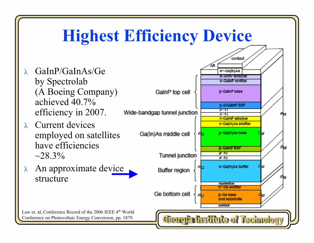
Law et. al, Conference Record of the 2006 IEEE 4th World Conference on Photovoltaic Energy Conversion, pp. 1879.
λ GaInP/GaInAs/Ge by Spectrolab (A Boeing Company) achieved 40.7% efficiency in 2007.
λ Current devices employed on satellites have efficiencies ~28.3%
λ An approximate device structure
Highest Efficiency Device

Energy of a PhotonE [eV] = hc = 1.24
λ λ[µm] c = 3×10⁸ [m/s]h = 6.626×10⁻³⁴ [J·s]
λis the wavelength of light in meters
J = 1.602×10⁻¹⁹ [eV]
Bandgap [eV] Wavelength [µm]
Ge 0.67 1.85
Si 1.12 1.107
GaAs 1.42 0.873
GaN 3.4 0.365

Photovoltaic Effectλ Solar cells are:
– p-n junctions – Minority carrier devices– Voltage is not directly applied
λ The photocurrent produces a voltage drop across the resistive load, which forward biases the pn junction.
R
P N--
--
--
+
+
+
hν
+ V -
IF
Itotal
IL
E-Field

Photovoltaic Effect
Power = V×I
Current
Absorption of light
Creation of additional
EHP
Voltage
Excitation of electrons
Separation by e- field
Movement in e- field
λ Fundamental absorption is from:– annihilation or absorption of photons by the excitation of an electron from
the valence band to the conduction band– leaves a hole in the valence band
λ Ideally, each incident photon with Ehν > EG will create one electron flowing in the external device
λ Ehν < EG : semiconductor is transparent to light

llumination and GenerationIncident light on a solar cell causes an electron to be excited from the valence band into the conduction band (creating electron-hole pairs) everywhere in the device. Ehν < EG : the device is transparent to the incident light.Ehν ≥ EG : photons are absorbed and EHP are photogenerated in the device.Ehν > EG : energy generated is lost as heat to the device.
hν
Ehν ≥ EGEhν < EG
EC
EVEhν > EG

Diode at Equilibrium
EC
EFEi
EV
Drift Diffusion
Diffusion Drift
-qVbi

Depletion RegionEvery EHP generated in the:
o Depletion region o Within a diffusion length (L = √Dτ) away from the depletion region are:
Swept across the junction by an electric field. Referred to as photocurrent and is in the “reverse bias” direction. All other EHP recombine before they can be collected.Photocurrent is always in the “reverse bias” direction, therefore the net solar cell current is also in the “reverse bias” direction.
ECEFEi
EV
-qVbi
Depletion Region
-xp xn

Drift
Diffusion
EC
EV
EFn
EFpEi
Diffusion
Drift
Forward Bias Photogeneration
Voltage is generated internallyfrom EHP being swept acrossthe junction by an electric field.Current is dominated by Drift.
Voltage applied externally.Current is dominated by Diffusion.
qVA
DriftDiffusion
EC
EV
EFn
EFpEi
Diffusion Drift
qVA

Law of the JunctionVA is the difference between Fermi level on the n-
side and the p-side when a voltage is applied to a pn junction.
VA = (kT/q)ln{(np(x=-xp)×pn(x=xn)/ni2}
It is related to the minority carriers in each region.VA will be the same in the forward bias case and in
the photogenerated case.

Current Collection
R
P N--
--
--
+
+
+
hν
+ V -
IF
Itotal
IL
E-Field
Itotal = IF – IL
= Is{exp(qV/kT) -1} – IL
IF = Forward-bias current
IL = Photocurrent
Is = Ideal reverse saturation current

λ Using the Ideal diode law: I = IO(e{qV/kT} – 1) λ I = IL – IO(e{[V+IrS]/nVT} – 1) – ({V + IrS}/rshunt)λ IL is the light induced current or short circuit current (ISC)λ VOC = kT/q (ln {[IL/IOC] +1})λ rS is the series resistance due to bulk material resistance and metal contact resistances.λ rSh is the shunt resistance due to lattice defects in the depletion region and leakage
current on the edges of the cell.λ VT = kT/qλ n – non ideality factor, = 1 for an ideal diode
Solar Cell Equivalent CircuitI
V_
+

λ Vm and Im – the operating point yielding the maximum power outputλ FF – fill factor – measure of how “square” the output characteristics are and used to
determine efficiency.FF = VmIm / VOCISC
λ η - power conversion efficiency.η = Pmax / Pin
= VmIm / Pin
= FFVOCISC / Pin
λ If EG↓ then: – More photons have the energy required
to create an EHP – ISC ↑ and VOC ↓
λ Large RS and low RShreduces VOC and ISC
IV Curves
V
I
ISC
VOCIm
Vm
LightDark

V
Log(I)
IO1
IO2 RSh
RS
IC Curves – Dark measurement

Highest Efficiency Device
1.8eV = 689nm
1.4eV = 886nm
0.67eV = 1850nm

Si Technologyλ Textured top layerλ Incident light will:
– Become trapped– Bounced around in the texture– Absorbed in the device
hν

Dr. Doolittle’s Solar Cell Research
Fabricated MBE InGaN solar cell with interdigitated grid contacts
Al2O3
Mg doped - GaN
Ni/Au contact
Ti/Al/Ti/Aucontact
Si doped - GaN
AlN
Si doped - InGaNundoped - InGaN
Schematic of the interdigitated grid contactsInGaN bandgap: 2.8eV = 442nm

What is a Tunnel Junction?

Tunnel JunctionTunnel junction requires degenerate doping!
EC
EV
Non-degenerately Doped
p nn
EC
EV
Degenerately Doped – highly material
p nn

EC
EF
EVSpace Charge Region
Energy-band diagram in thermal equilibrium – n and p-region are degenerately doped
EC
EV
e-
e-
Large forward-bias voltage – the maximum number of electrons in the n-region is opposite the maximum number of empty states in the p-region; maximum tunneling current is produced.
Increased forward-bias voltage – the number of electrons directly opposite the holes decreases and the tunneling current decreases.
Tunnel Junction

Non-IdealitiesBulk defects – dislocations and stacking faults, due to lattice mismatch with the substrate. Surface recombination defects – EHP generated by the absorption of light can recombine before they cross the junction, therefore not contributing to the power output of the solar cell.Bulk recombination defects – EHP generated further away from the junction have a large probability of recombining before they reach the device terminals.Insufficient photon energy: hν < EgExcessive photon energy : hν > EgSolar cell is too thin – some of the light of the appropriate energy is not coupled into the cell and is passed through the device.Open circuit Voltage (VOC) losses – recombination of EHP in trap levels in the depletion region that lowers VOC.Fill Factor losses – related to VOC, series resistance, and shunt resistance.Reflection losses

Anti-Reflection Coating
Prevents incident light from reflecting off of the device.The AR coating needs to have the correct refractive index for the material system and be transparent.Deposited as noncrystalline or amorphous layer which prevents problems with light scattering at grain boundaries.A double layer AR coating reduces the reflection of usable sunlight to ~ 4%.