Solar Cell Nanotechnology (Tiwari/Solar) || Control of ZnO Nanorods for Polymer Solar Cells
23
135 Atul Tiwari, Rabah Boukherroub, and Maheshwar Sharon (eds.) Solar Cell Nanotechnology, (135–158) 2014 © Scrivener Publishing LLC 5 Control of ZnO Nanorods for Polymer Solar Cells Hsin-Yi Chen 1 , Ching-Fuh Lin 1,2, * 1 Graduate Institute of Photonics and Optoelectronics Engineering, National Taiwan University, Taipei, Taiwan (R.O.C.) 2 Graduate Institute of Electronics Engineering, National Taiwan University, Taipei, Taiwan (R.O.C.) Abstract Zinc oxide (ZnO), an n-type inorganic semiconductor, has been exten- sively utilized in polymer solar cells due to its salient characteristics such as low cost, non-toxicity, high stability, and good optoelectronic proper- ties. Their one-dimensional counterparts, ZnO nanorods (NRs), are par- ticularly attracting more and more attention in recent years. Compared with devices in a planar configuration, this device architecture has sev- eral advantages, including that the morphology of the composite can be controlled in a systematic and reproducible way; devices using vertically- aligned ZnO NRs can increase electron donor/acceptor interface areas; and this device structure provides direct electron transport pathways toward the electrode that possesses high electron mobility. Therefore, the understanding of ZnO NRs for the control of polymer solar cells is criti- cal. In this chapter, we will review the preparation, characterization and morphology control of ZnO NRs. The latest technology and principles of utilizing ZnO NRs to enhance device performance in polymer solar cells will also be reported in detail. Keywords: Zinc oxide (ZnO), nanorod (NR), morphology, polymer solar cell *Corresponding author: cfl[email protected]
Transcript of Solar Cell Nanotechnology (Tiwari/Solar) || Control of ZnO Nanorods for Polymer Solar Cells

135
Atul Tiwari, Rabah Boukherroub, and Maheshwar Sharon (eds.) Solar Cell Nanotechnology, (135–158) 2014 © Scrivener Publishing LLC
5
Control of ZnO Nanorods for Polymer Solar Cells
Hsin-Yi Chen1, Ching-Fuh Lin1,2,*
1Graduate Institute of Photonics and Optoelectronics Engineering, National Taiwan University, Taipei, Taiwan (R.O.C.)
2Graduate Institute of Electronics Engineering, National Taiwan University, Taipei, Taiwan (R.O.C.)
AbstractZinc oxide (ZnO), an n-type inorganic semiconductor, has been exten-sively utilized in polymer solar cells due to its salient characteristics such as low cost, non-toxicity, high stability, and good optoelectronic proper-ties. Their one-dimensional counterparts, ZnO nanorods (NRs), are par-ticularly attracting more and more attention in recent years. Compared with devices in a planar confi guration, this device architecture has sev-eral advantages, including that the morphology of the composite can be controlled in a systematic and reproducible way; devices using vertically-aligned ZnO NRs can increase electron donor/acceptor interface areas; and this device structure provides direct electron transport pathways toward the electrode that possesses high electron mobility. Therefore, the understanding of ZnO NRs for the control of polymer solar cells is criti-cal. In this chapter, we will review the preparation, characterization and morphology control of ZnO NRs. The latest technology and principles of utilizing ZnO NRs to enhance device performance in polymer solar cells will also be reported in detail.
Keywords: Zinc oxide (ZnO), nanorod (NR), morphology, polymer solar cell
*Corresponding author: cfl [email protected]

136 Solar Cell Nanotechnology
5.1 Introduction
Organic solar cells (OSCs) are good alternatives compared to con-ventional inorganic photovoltaic devices because they can be fabri-cated on fl exible substrates by solution process. However, in order to overcome the short exciton diffusion length in most organic semi-conductors, a bulk heterojunction (BHJ) structure is widely utilized in organic solar cells. In terms of BHJ cells, poly(3-hexylthiophene) (P3HT) and (6, 6)-phenyl C61 butyric acid methyl ester (PCBM) are the most commonly utilized materials for electron donor and acceptor with a high power conversion effi ciency (PCE) of 5% [1–3]. A number of inorganic semiconductors, such as TiO2 [4, 5], ZnO [6, 7] and CdSe [8] have also been applied as electron acceptors. Although effi cient charge separation is achieved by a large inter-facial area between electron donor and acceptor, BHJ devices usu-ally suffer from discontinuous charge transport pathways [9]. In addition, the percolation network is susceptible for process, which makes it diffi cult to achieve a reliable performance. Consequently, creation of vertically-aligned inorganic nanostructures with respect to the substrate is thus considered to be a potential approach to overcome the above disadvantages.
In an ideal case, vertically-aligned nanostructures could be syn-thesized with an optimized dimension which is short enough for the most excitons to diffuse through the interface between the inor-ganic and organic materials. By controlling the dimension of the vertically-aligned nanostructure, polymer chains are also allowed to align themselves perpendicular to the substrate. The inter-chain cou-pling is thus improved, causing better exciton diffusion and charge transport in conjugated polymers [10–12]. On the other hand, for electrons, there is also a direct transport pathway to reach the elec-trode in vertically-aligned nanostructures. Among those nanostruc-tures, ZnO NRs are the most extensively utilized nanostructures for organic solar cells in the past few years due to their excellent opti-cal characterization, good structural property, large-area availability and low cost synthesis process. As a result, in this chapter, we will review the recent work focusing on the control of ZnO NRs for poly-mer solar cells. The preparation, characterization and morphology control of ZnO NRs will be demonstrated. The latest technology and principle by utilizing ZnO NRs to improve the surface morphology and enhance charge separation in polymer solar cells (PSC) will also be addressed in detail in this chapter.

Control of ZnO Nanorods for Polymer Solar Cells 137
5.2 Preparation and Characterization of ZnO NRs
ZnO are receiving considerable interest because of their excel-lent photonic properties, as well as a wide bandgap of 3.4 eV that is benefi cial to short wavelength optoelectronic applications. Its transparent property is also good for visible light transmis-sion. Its nanostructure counterparts, ZnO NRs, are able to facili-tate more effi cient carrier transport because of decreased grain boundaries, surface defects, disorders, and discontinuous inter-faces [13, 14]. Conventionally, various methods of growing ZnO NRs include vapor liquid-solid (VLS) deposition and chemical vapor deposition (CVD) [15]. So far, the simplest, most energy-effi cient method for synthesizing ZnO NRs is using the hydro-thermal method [15, 16]. This technique has been shown to be the most economical synthesis process compared to the conven-tional growth method [16]. Consequently, in terms of the prepa-ration of ZnO NRs, we will focus on the ZnO NRs preparation and characterization by hydrothermal method in the following section.
5.2.1 ZnO NRs Prepared by Hydrothermal Method
The hydrothermal method is generally regarded as a solution-phase synthesis compared to vapor-phase synthesis. The growth process is carried out in a liquid. Normally aqueous solutions are introduced and the process is then referred to as “hydrothermal” growth process. Some of the solution-phase synthesis processes are Zinc Acetate Hydrate (ZAH) derived nanocolloidal sol-gel route [17], ZAH in alcoholic solutions with sodium hydroxide (NaOH) or tetra methyl ammonium hydroxide (TMAH) [18–20] and template-assisted growth [21].
So far, the general hydrothermal process to synthesize ZnO NRs is as follows: Si (or alternative substrate) is cleaned by a stan-dard cleaning method. Approximately 200–500 nm ZnO thin fi lm is deposited on the substrate using RF magnetron sputtering at room temperature. The samples are then heated in air at various temperatures (250–450°C) for 10–30 min to obtain ZnO seeds for hydrothermal growth. Other method like sol-gel processes can also be applied to form this thin fi lm of seed layer [17]. ZnO nanopar-ticles have also been used for the seed layer by directly coating the

138 Solar Cell Nanotechnology
solution that contains the suspended colloidal nanoparticles on the substrates, followed by a simple annealing step to remove the sol-vent [21]. The ZnO-seeded samples are then placed in a solution containing zinc nitrate (Zn(NO3)2) and hexamethylamine (HMT) as a precursor. The hydrothermal reaction is usually performed in a preheated oven at a certain temperature (usually < 100°C) for sev-eral hours. In the hydrothermal process, several factors are often considered to affect the synthesis of the ZnO NRs, including control of HMT and Zn(NO3)2, control of seed layer synthesis and heating temperature, as well as morphology control of ZnO NRs. Herein we will discuss the above three important parameters to obtain excellent ZnO NRs.
5.2.1.1 Control of HMT and Zn(NO3)2
Vayssieres et al. [22] fi rst utilized the hydrothermal method for the controlled fabrication of ZnO NRs on glass and Si substrates by the thermal decomposition of methenamine and zinc nitrate. To initi-ate the growth from the substrate, a thin layer of ZnO nanoparticles is put on the substrate. Methenamine, also known as hexamethy-lenetetramine (HMT), is a highly water soluble, non-ionic tetraden-tate cyclic tertiary amine. Thermal degradation of HMT releases hydroxyl ions which react with Zn2+ ions to form ZnO [23]. This can be described in the following equations:
(CH2)6N4 + 6H2O 6HCHO + 4NH3, (5.1)
NH3 +H2O NH+4 +OH−, (5.2)
2OH− + Zn2+ ZnO(s) +H2O. (5.3)
It is generally known that the role of HMT is to supply the hydroxyl ions to drive the precipitation reaction [24]. Besides, HMT also acts as a buffer as the rate of its hydrolysis decreases with an increase in the pH value [25]. Ashfold et al. [24] have demonstrated that the rate of decomposition of HMT is independent of the reaction and that HMT does act as a kinetic buffer. In the initial growth stage, the pH value and the concentration of Zn2+ ions are higher so that the ZnO growth will be through Zn(OH)2. With the gradual increase in the pH value and the concentration of the Zn ions, Zn(OH)2 becomes ther-modynamically unstable and the Zn(OH)2 formed on the substrate begins dissolving. Further growth of the NRs will be through direct

Control of ZnO Nanorods for Polymer Solar Cells 139
deposition of ZnO [24]. The contribution of HMT in the growth pro-cess of ZnO NRs has also been discussed by Sugunan et al. [26]. It was proposed that HMT, a long-chain polymer and a nonpolar chelating agent, will preferentially attach to the nonpolar facets of the zincite crystal. Therefore, it cuts off the access of Zn2+ ions to them, leaving only the polar (001) face for epitaxial growth. That is, HMT acts more like a shape-inducing polymer surfactant rather than as a buffer.
There is a lot of research investigating the growth mechanism of ZnO NRs synthesized using Zn(NO3)2 and HMT, such as the effect of substrates and seed layers on the morphology of nanorods [27–29], as well as the control of aspect ratio through the addition of citrate anions [30]. Pal and Santiago [31] have controlled the mor-phology of ZnO nanostructures by varying the amount of a soft sur-factant, ethylenediamine and the pH value of the reaction mixture composed of sodium hydroxide and the surfactant. Homogenous growth was observed at a pH value of 12 with inhomogeneity creeping as the pH decreases [31]. A 10% concentration of ethyl-enediamine obtained higher aspect ratio than 5% concentration. ZnO NRs have been successfully synthesized using different sur-factants which are available from numerous reports. Tang et al. [32] synthesized ZnO NRs by using zinc acetylacetonate Zn(acac)2 ·H2O as a single source precursor and investigated the growth condition of the nanorods in the presence of four different surfactants: poly-vinyl alcohol (PVA), polyethylene glycol (PEG), sodium dodecyl sulphate (SDS) and cetyltrimethyl ammonium bromide (CTAB). The usage of PVA resulted in more regular and defect-free rods than PEG, SDS and CTAB. Li et al. [33] have reported the growth of tapered ZnO NRs with diameter decreasing from 400 nm at the body to about 80 nm at the tip from CTAB-assisted hydrothermal growth. Chen et al. [34] studied the effect of potassium iodide (KI) as a surfactant in the crystallization of ZnO nanorod clusters from a chemical bath containing zinc nitrate hexahydrate and hydrazine hydrate. They obtained step growth of hexagonal nanorod clusters, which is attributed to the presence of iodine ions in the growth bath. The further results clearly demonstrated that the source of Zn ions could also affect the morphology. Ni et al. [35] obtained ZnO NRs in place of stepped columns simply by changing the source of Zn ions from Zn(Ac)2 to ZnCl2, and all other conditions remain. It is noted that the presence of Zn2+ containing salts is not a necessity for the growth of ZnO nanostructures through the hydrothermal growth method. Li et al. [36] have successfully grown large-scale arrays of

140 Solar Cell Nanotechnology
ZnO NRs on zinc foil without the assistance of any template, oxi-dant or coating of metal oxide layers. It is simply synthesized by dipping the foil into a 25% aqueous solution of ammonia and heat-ing at a temperature 80°C in a Tefl on-lined stainless steel autoclave. From the above research, it was observed that the thickness, den-sity and morphology of the ZnO NRs are affected by the pH value and the concentration of HMT and Zn(NO3)2 in the growth bath. A good understanding of control of HMT and Zn(NO3)2 can promote high quality ZnO NR growth.
5.2.1.2 Control of Seed Layer Synthesis and Heating Temperature
In this hydrothermal method technique, the seeded substrates are utilized to achieve well-controlled morphology and growth orien-tation of ZnO NRs. Heterogeneous nucleation can favor the ZnO NR growth because the interfacial energy between crystals and substrate is usually smaller than the interfacial energy between crystals and solution [37]. Therefore, pre-coating the substrate with seed materials that are similar to nanocrystals can effectively con-trol nanorod orientation and morphology.
A variety of methods have been employed to produce seeds such as thermal evaporation [14, 15], metal organic chemical vapor depo-sition (MOCVD) [38–40], spin coating [41], and sputtering [42–46]. Li et al. [42] and Song et al. [43] deposited ZnO on silicon substrate by using RF sputtering followed by hydrothermal reaction without any heat treatment and obtained columnar ZnO NRs. The above results show the importance of the heat treatment of ZnO seed lay-ers in forming ZnO NRs using the hydrothermal method. ZnO NRs have been grown on a seeded Zn sheet, and the optimum ZnO seed formation was obtained after oxidation at 300°C [15]. Above 300°C, ZnO fl akes other than spherical ZnO seeds form on the Zn sheet. For a Zn thin fi lm sputtered on PTFE substrate, thermal oxidation was performed at 300°C followed by hydrothermal reaction to grow ZnO NRs. Liu et al. [46] used ZnO deposited on Si substrate by ion beam sputtering followed by annealing temperature at 200–600°C. The high annealing temperature could limit future applications of ZnO NRs because the ZnO buffer layer would degrade. This degra-dation can be caused by interdiffusion between the buffer layer and the Si substrate, and by the thinning of the buffer layer because of heating at high temperature [47].
Control of ZnO Nanorods for Polymer Solar Cells 141
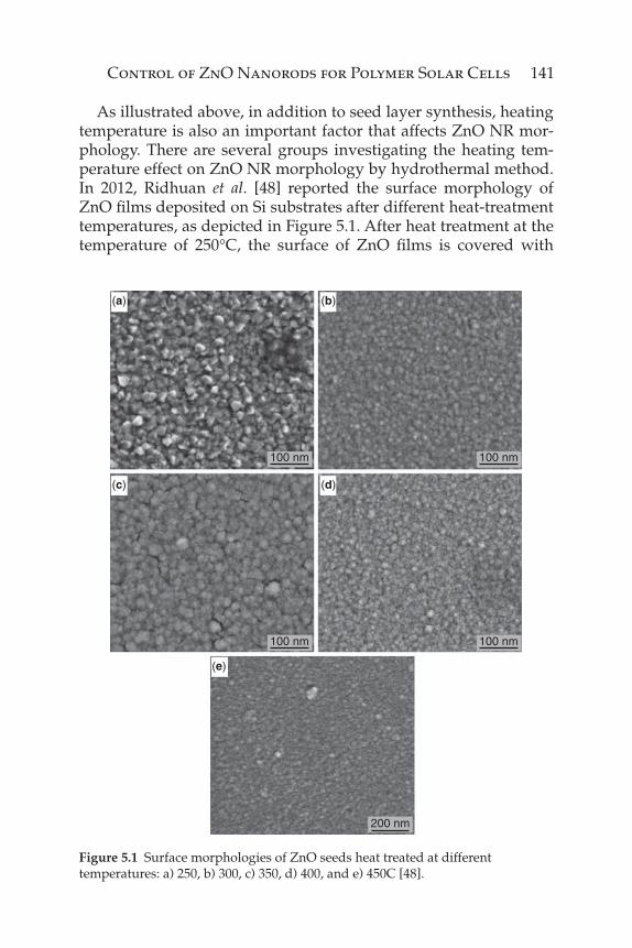
As illustrated above, in addition to seed layer synthesis, heating temperature is also an important factor that affects ZnO NR mor-phology. There are several groups investigating the heating tem-perature effect on ZnO NR morphology by hydrothermal method. In 2012, Ridhuan et al. [48] reported the surface morphology of ZnO fi lms deposited on Si substrates after different heat-treatment temperatures, as depicted in Figure 5.1. After heat treatment at the temperature of 250°C, the surface of ZnO fi lms is covered with
(a) (b)
(c)
(e)
(d)
100 nm 100 nm
100 nm
200 nm
100 nm
Figure 5.1 Surface morphologies of ZnO seeds heat treated at different temperatures: a) 250, b) 300, c) 350, d) 400, and e) 450C [48].

142 Solar Cell Nanotechnology
dispersed particulate grain size and an average diameter of 90 nm is obtained. The surface morphology of ZnO seed layer transforms from a fl aky structure at 250°C to a circular structure with heat-ing temperature increasing from 300°C to 450°C [48]. Obviously, the ZnO seed size decreases with increased heating temperature. With high heating temperature treatment, the seed layer particles tend to dislocate and pile up. At high heating temperatures, atoms vibrate at their lattice positions and exchange energy with neigh-boring atoms. As the atoms reach suffi cient energy, they diffuse to achieve the lowest strain energy and form small seeds. That is, smaller grains form with increasing heating temperature. On the other hand, to achieve excellent nanorod formation by the hydro-thermal method, ZnO seeds need to have uniform size and distri-bution. The ZnO seeds are required to provide enough spaces for ZnO nanorod growth during a hydrothermal reaction. From the FESEM images in Figure 5.2, the ZnO seeds which are treated at 400°C depict the best morphology for ZnO NRs formation.
The heat-treated seeded substrates are then subjected to hydro-thermal growth at 80°C for 4 h to investigate the ZnO seeds effect on ZnO NRs formation. Figures 5.2(a)–5.2(e) [48] illustrate ZnO NRs growth on ZnO seed substrates at different heating tempera-tures corresponding to Figure 5.1. The average lengths of ZnO NRs are 105, 184, 231, 742, and 605 nm for ZnO seeds heat treated at 250, 300, 350, 400, and 450°C, respectively [48]. The average diam-eter of the ZnO NRs gradually increases from 64 nm to 80 nm with increased heating temperature of the seed layer. The increase in ZnO nanorod length is due to increasing reactivity of the seed layer surface during the nucleation stage [46]. Generally, the ZnO crystal structure consists of a number of alternating planes com-posed of coordinated Zn and O atoms along the c-axis direction. The Zn-terminated [0001] is at the top surface of the ZnO crystal structure, whereas the O-terminated [000)] is at the bottom surface, causing a dipole moment and a polar surface of ZnO seed layer [46]. As a result, the presence of two charges (Zn2+ and OH- ions) results in the polar surface of the ZnO seed layer.
On the other hand, because Zn(OH)2 forms and produces ZnO upon dehydration, the increased heating temperature can effec-tively improve the reactivity of the seed layer. This reactivity is stronger than the electrostatic interaction of the polar surface of the ZnO seed layer with the charges (Zn2+ and OH-) because of the energy supplied during heat treatment [46]. Therefore, more

Control of ZnO Nanorods for Polymer Solar Cells 143
Zn2+ and OH- ions are diffused on the ZnO seeds, which bring out increased ZnO nanorods length with heating temperature from 250°C to 400°C. However, further increase annealing temperature to 450°C results in decreased ZnO nanorod length. It clearly dem-onstrates that there is a threshold annealing temperature for the ZnO seed layer which leads to the structural deterioration.
The X-ray diffraction spectra of ZnO NRs with different heating temperatures are also shown to identify the structural property [48].
(a) (b)
(c)
(e)
(d)
100 nm 100 nm
200 nm
200 nm
200 nm
Figure 5.2 FESEM images of ZnO NRs grown on seeds heat treated at different temperatures: a) 250, b) 300, c) 350, d) 400, and e) 450C [48].

144 Solar Cell Nanotechnology
It illustrates two peaks corresponding to wurtzite ZnO with a strong (002) peak and a small (103) peak at 2θ= 34.4° and 61.7°, respectively. It is depicted that the (002) peak intensity increases with the rising heating temperature. This is because, when the annealing temper-ature increases, more energy is supplied, thus causing Zn and O atoms to move into the proper sites. As a result, the crystal quality is improved to reduce the Gibbs free energy and high-quality ZnO crystals are formed under thermal equilibrium [47]. As mentioned above, Figure 5.1 demonstrates that the increased heating tempera-ture produces smaller ZnO seeds. A larger ratio of the surface area to volume also increases the surface area, thus increasing the ZnO growth rate. On the other hand, it demonstrates that the peak shifts to a slightly higher 2θ from 34.2°
to 34.6° at higher temperature [48]. This
may be due to the release of intrinsic strain induced by the presence of residual strain from structural imperfections, such as vacancies, stacking faults, and interstitials. According to the research investiga-tion by Shin et al. [39], the lattice mismatch between ZnO fi lm and Si-substrate could cause structural defects during the growth. Thus, an annealing treatment of the ZnO fi lm deposited on Si-substrate could remove the intrinsic strain because the Zn and O atoms would be stacked in order. From the above results and discussions, the good control of seed layer synthesis and heating temperature for ZnO NRs growth by hydrothermal method is shown to be of great importance.
5.2.2 Morphology Control of ZnO NRs
As generally known, ZnO is regarded as a polar crystal. In its crys-tal structure, O2− is in hexagonal closest packing and each Zn2+ lies within a tetrahedral group of four oxygen ions [49]. Zn and O atoms are stacked alternatively along the c-axis. The formation of hexago-nal prism and pyramid of ZnO crystals is attributed to the differ-ence in the growth velocities of various crystal facets. The growth velocities under hydrothermal conditions along the different direc-tions are known to follow the relation V(0001) > V(1011) > V(1010) [50]. Therefore, the relative growth rate of these crystal faces will determine the fi nal shape and aspect ratio of the ZnO NRs.
Besides the ZnO NRs morphology affected by growth velocity in different directions, it is also signifi cant to address the mechanism to bring out different morphology of ZnO NRs infl uenced by differ-ent Zn(NO3)2 concentration and reaction time. Li et al. [51] proposed the formation mechanism of ZnO NRs effected by different Zn(NO3)2

Control of ZnO Nanorods for Polymer Solar Cells 145
concentration and reaction time. In their experiment, the ZnO NRs are synthesized by a simple solution-phase method in two different kinds of solution [51]. The fi rst solution contained 1.5 g ammonia (25.0%) and 5 g Zn(NO3)2·6H2O (99.0%), and the second one contained 1.5 g ammonia and 3 g Zn(NO3)2·6H2O. Then two 2×3 cm2 zinc foils were put into the above two kinds of aqueous solution, respectively, followed by 12 hours heating at a constant temperature of 80°C.
The formation mechanism and the schemes have been illustrated in Figure 5.3 and Figure 5.4, respectively [51]. The only difference in the two conditions is that the added Zn(NO3)2·6H2O is less in the second solution. Therefore, the zinc precursor for the growth of ZnO crystals in the second solution mainly comes from the metal zinc, which leads to the supply of Zn2+ from Zn(NO3)2·6H2O being very little. Then the zinc precursor is transported from the root regions of NRs to the top regions because of the gradient of concentration. As a result, the lower concentration region is around the tops of NRs. The growth of ZnO crystals is relatively slow compared with the root of NRs, thus causing the formation of ZnO NRs with sharp tops (Figure 5.3(b)). On the other hand, for the fi rst solution with more Zn(NO3)2·6H2O, there is almost no gradient of concentration.
Crystalline grains
Crystalline grains
Diffusion of zinc precursor fromzinc foil and Zn(NO3)2•6H2O
Diffusion of zinc precursorfrom zinc foil
(a)
(b)
Figure 5.3 Growth diagram of the ZnO NRs (a) with fl at-top for 12 h in the fi rst solution; (b) with sharp-top for 12 h in the second solution. [51].

146 Solar Cell Nanotechnology
The concentration of zinc precursor is uniform throughout, which results in the formation of ZnO NRs with fl at tops (Figure 5.3(a)).
Furthermore, with increasing reaction time, it also brings out different morphology as shown in Figure 5.4. As two single NR contact with each other, the local supersaturation of the solution is enhanced, which results in the secondary growth of crystals around the interface between the two NRs [52], and then the fl at-top nanorods are formed reasonably well. On the other hand, the lath-like nanorods are also found during the growth, as shown in Figure 5.4(b). From the viewpoint of crystal growth, the six crystal planes have the same growth speed and it can not extend two crys-tal planes in one direction [53]. However, as shown in Figure 5.4(b), when two fl at-top nanorods are closely parallel to each other, the secondary growth of crystals will happen in the interface regions and carry out the coalescence. If this situation continues, a lath-like crystal will be obtained thereby. It can elucidate the lath-like crystal which happens with the increasing reaction time.
5.2.3 Summary of ZnO NR Growth
The hydrothermal method is so far the simplest and most effi -cient process to synthesize ZnO NRs. Various additives are used
Sharp-top Flat-top
Flat-top Lath-like
(a)
(b)
Figure 5.4 Mechanism of the morphology transition of ZnO NRs with increasing reaction time in the second solution. [51].

Control of ZnO Nanorods for Polymer Solar Cells 147
in aqueous medium to successfully synthesize ZnO NRs of dif-ferent morphologies. A mixture of Zn(NO3)2 and HMT is the most popular solution in the growth process. Based on the investigations above, ZnO NRs are attractive candidates for applications in opto-electronic devices such as solar cells, sensors, and energy genera-tors. Good control of HMT and Zn(NO3)2, seed layer synthesis and heating temperature is benefi cial to synthesize excellent vertically-aligned ZnO NRs, which can promote higher device effi ciency in organic solar cells.
5.3 Application of ZnO NR in Polymer Solar Cells
In the past decade, rapid progress in the development of polymer solar cells has raised the power conversion effi ciency from 3% to almost 9%, refl ecting a promising future for production possibility. Polymer solar cells are processed from solution in organic solvents, whereas small molecule solar cells are usually processed using thermal evaporation deposition that requires vacuum equipment. Besides, PSCs are considerably attractive owing to a number of advantageous features, including thin-fi lm architecture, less mate-rial consumption, and low manufacturing energy demands. On the other hand, as mentioned previously, vertically-aligned inorganic nanostructures are considered to be a practical method for promot-ing effi cient charge transport in organic solar cells. As a result, over the recent years, ZnO NRs are extensively utilized in polymer solar cells to form organic-inorganic hybrid solar cells (HSC).
Organic-inorganic HSCs, which use a combination of organic and inorganic semiconductors, have been widely studied as an alternative to fully OSCs. This type of solar cell has been achieved by combining organic materials and inorganic semiconductors together. In general cases, a p-type organic semiconductor usually serves as both light harvester and electron donor, and the n-type inorganic semiconductor serves as electron acceptor. HSCs device structure possesses some advantages compared to OSCs. For exam-ple, the inorganic semiconductor of HSCs usually has higher elec-tron mobility than the counterpart of organic materials. Besides, inorganic semiconductors usually have higher physical and chemi-cal stability compared to that of organic semiconductors. Among these n-type inorganic semiconductors, ZnO has attracted a lot of attention in HSCs because it is less toxic than many other II–VI

148 Solar Cell Nanotechnology
semiconductors and is relatively easy to synthesize in large quan-tities with low cost techniques. As an n-type semiconductor with a wide bandgap, ZnO also has very good optical property, which makes ZnO an excellent candidate as a good cathode buffer layer (CBL) or a transparent electrode in HSCs. In this section, we will report on the recent development of solar cells containing ZnO NRs and organic semiconductors. We will focus on the research of pho-tovoltaic devices where ZnO acts as an electron acceptor or elec-trode buffer layer and transparent electrode.
5.3.1 ZnO-NR/Polymer Solar Cells Based on Vertically-Aligned Zno NRs
Compared with photovoltaic devices with a planar confi guration, this kind of device confi guration has several advantages. For instance, the morphology of the composite can be controlled in a reproducible way through controlling ZnO NR growth. The devices using vertically-aligned ZnO NRs can increase electron donor/acceptor interface areas, which can create direct electron transport pathways toward the electrode. Olson et al. fi rst reported the study on ZnO-NR/P3HT HSCs based on vertically-aligned ZnO NRs in 2006 [54]. ZnO/P3HT HSCs with this device structure produced a VOC of 0.44 V, a JSC of 2.2 mA/cm2, a fi ll factor (FF) of 0.56, and a PCE of 0.53%. They also investigated the effect of polymer on ZnO-NR/P3HT solar cell per-formance. The device performance was improved when dichloro-benzene was used as the solvent instead of chloroform, due to the enhanced infi ltration. Furthermore, they reported that thermal annealing can improve the infi ltration of the P3HT into the ZnO NRs, which is one of the most important issues for solar cells with this ver-tically-aligned NR structure [55]. Figure 5.5 depicts the cross-sectional SEM images of ZnO-NR/P3HT solar cells with and without anneal-ing. It clearly indicates that the infi ltration of the P3HT polymer is improved with increasing annealing temperature. It is also observed that more P3HT polymer adheres to the ZnO NRs for annealed cases after removing the polymer on top of the NRs.
In addition to P3HT, another polymer semiconductor poly(1-methoxy-4-(2ethylhexyloxy)-p-phenylenevinylene) (MEH-PPV) has also been utilized in this kind of device. ZnO-NR/MEH-PPV with vertically-aligned ZnO NRs has been reported by Wang et al. They prepared high quality ZnO NRs with low defect concentrations by electrodeposition method [56]. In order to further improve device

Control of ZnO Nanorods for Polymer Solar Cells 149
performance of ZnO-NR/organic HSCs, a lot of approaches have been investigated to modify and optimize the ZnO-NR/organic inter-face [57–59]. Furthermore, the ZnO surface can be modifi ed by coating with a thin layer of other materials. The electrical properties of ZnO can be well controlled by the different doping level or coating com-position. Various doping and surface treatment methods are demon-strated to modify the performance of HSCs with this device structure. For example, Ravirajan et al. [60] demonstrated the characterization of dye modifi ed ZnO-NR/polymer solar cells with vertically-aligned NRs acting as electron acceptor materials. Three different solution chemicals were investigated for the synthesis of ZnO. An amphiphilic polypyridyl ruthenium complex dye was used to modify interfacial electron transfer between P3HT and the ZnO nanostructure surface,
Ag
(a) (d)
(d) (e)
(c) (f)
P3HT
ZnO
Figure 5.5 Cross-sectional SEM images of P3HT/ZnO NRs composite PV devices: (a) without annealing; (b) with annealing at 150 C; (c) with annealing at 225 C. Also shown are images after removing the polymer on top of the rods: (d) no anneal; (e) annealing at 150 C; (f) annealing at 225 C. Scale bars: 200 nm [55].
150 Solar Cell Nanotechnology
resulting in improved device performance compared to devices with-out dye treatment. The improvement is probably due to slower charge recombination after the amphiphilic dye modifi cation treatment [60]. Other than these organic materials, inorganic coating has also been uti-lized to improve the device performance of ZnO-NR/organic HSCs. For example, Xu et al. [61] reported a simple and low-cost electrodepo-sition method to deposit n-type CdSe on the ZnO surface. ZnO-NR/P3HT solar cells with vertically-aligned ZnO NRs coated by CdSe exhibited an improved PCE of 0.88%, with short-circuit current den-sity (Jsc) 4.89 mA/cm2 and open-circuit voltage (Voc) of 0.51 V [61].
5.3.2 ZnO NR as a Cathode Buffer Layer in Polymer Solar Cells
In addition to acting as electron acceptor material in the active layer of ZnO/organic solar cells, ZnO can also be used as an cathode buf-fer layer (CBL) as well as a transparent electrode, which has attracted increasing attention during the past fi ve years. As mentioned previ-ously, ZnO is one of the n-type semiconductors with a wide bandgap of 3.4 eV, exhibiting attractive features such as high electron mobil-ity, good optical transmittance, and excellent stability [62]. It also has attractive features such as non-toxicity, low cost process and large-scale area availability. Using ZnO as a CBL in solar cells can enhance the PCE by collecting and extracting electron carriers, as well as blocking positive hole carriers. Therefore, the ZnO is sometimes regarded as electron transport layer or hole blocking layer besides CBL. Furthermore, such ZnO CBL is considered as the optical spacer and oxygen barrier in solar cell devices to enhance their stabilities and lifetimes, which effectively improves the overall device performance [63, 64]. As a result, great efforts have been carried out to improve the performance of organic/inorganic HSCs by using ZnO NRs [65–67].
ZnO NRs were developed with an important role to construct an effi cient CBL in polymer solar cells. Using ZnO NRs layer instead of a ZnO planar structure brings out the rapid collection of generated carriers because the ZnO NRs provide a directly conducting and ordered path from the point of photogeneration to the electrode, thus effectively reducing the electron recombination losses and improving the device performance [68]. It is particularly noted that, so far, ZnO NR are applied more often in inverted structure solar cells than conventional solar cells because of the stability issue. In conventional solar cells, it has been proven that acidic PEDOT:PSS
Control of ZnO Nanorods for Polymer Solar Cells 151
layer is detrimental to the organic layer [69–71], and the low work function metal cathode is easily oxidized in air even with a delicate encapsulation [69, 72]. To effectively ameliorate the stability of con-ventional structure, a new device design of inverted HSC is pro-posed [73, 74]. Therefore, we will focus here on the recent research of ZnO NR utilized in inverted polymer solar cells.
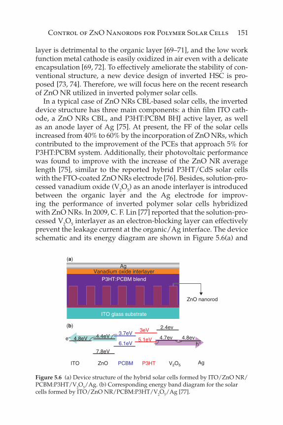
In a typical case of ZnO NRs CBL-based solar cells, the inverted device structure has three main components: a thin fi lm ITO cath-ode, a ZnO NRs CBL, and P3HT:PCBM BHJ active layer, as well as an anode layer of Ag [75]. At present, the FF of the solar cells increased from 40% to 60% by the incorporation of ZnO NRs, which contributed to the improvement of the PCEs that approach 5% for P3HT:PCBM system. Additionally, their photovoltaic performance was found to improve with the increase of the ZnO NR average length [75], similar to the reported hybrid P3HT/CdS solar cells with the FTO-coated ZnO NRs electrode [76]. Besides, solution-pro-cessed vanadium oxide (V2O5) as an anode interlayer is introduced between the organic layer and the Ag electrode for improv-ing the performance of inverted polymer solar cells hybridized with ZnO NRs. In 2009, C. F. Lin [77] reported that the solution-pro-cessed V2O5 interlayer as an electron-blocking layer can effectively prevent the leakage current at the organic/Ag interface. The device schematic and its energy diagram are shown in Figure 5.6(a) and
Ag
Ag
Vanadium oxide interlayer
P3HT:PCBM blend
ZnO nanorod
ITO glass substrate
ITO
(a)
(b)
ZnO
4.8eVe– 4.4eV 3.7eV3eV 2.4ev
4.7ev 4.8evh+
5.1eV6.1eV
7.8eV
PCBM P3HT V2O5
Figure 5.6 (a) Device structure of the hybrid solar cells formed by ITO/ZnO NR/PCBM:P3HT/V2O5/Ag. (b) Corresponding energy band diagram for the solar cells formed by ITO/ZnO NR/PCBM:P3HT/V2O5/Ag [77].

152 Solar Cell Nanotechnology
(b), respectively. The power conversion effi ciency is improved from 2.5% to 3.56% by the introduction of the V2O5 interlayer [77]. The interlayer also serves as an optical spacer to enhance light absorp-tion, and thereby increases the photocurrent. Moreover, the mixture structure by incorporating different transition metal oxides could also effi ciently enhance the device effi ciency. In 2010, C. F. Lin fi rst demonstrated mixed oxides as anodic modification through sim-ple solution processing to improve the efficiency and stability of inverted polymer photovoltaic devices [78]. The measured device performance is shown in Figure 5.7. The control device exhibits a Jsc of 10.67 mA/cm2, a Voc of 0.53 V, and an FF of 54.82%, resulting in a PCE of 3.1%. Either V2O5 or WO3 inserted, the device perfor-mance is improved (PCE of 3.74% for WO3 and 3.81% for V2O5). When the mixed oxides are introduced, the device has a signifi cant improvement, so Jsc increases to 11.97 mA/cm2, Voc to 0.56 V, and FF to 62.06%. Therefore, the PCE is notably improved to 4.16%, a 34% enhancement. These investigations show that the mixed oxides can suppress the leakage current, enhance the light absorption, and provide a temporally durable device.
It was found that the solidifi cation time of the active layer could also infl uence the device performance of inverted polymer/ZnO NRs solar cells. By slow drying the active layer, a device effi ciency
0.0
–12
–10
–8
–6
–4
–2
0
0.1
Control device
V2O5
WO3
WO3–V2O5mixed oxides
0.2 0.3 0.4Voltage (V)
Cu
rren
t d
ensi
ty (
mA
/cm
2 )
0.5 0.6
Figure 5.7 J-V curves of the photovoltaic devices shown in Figure. 5.6 with the different anode modifi cation under 100 mW/cm2 AM 1.5G irradiation [77].
Control of ZnO Nanorods for Polymer Solar Cells 153
of 3.58% was achieved, which could be attributed to the enhanced crystallinity of the polymer and the infi ltration of the active mate-rials [79]. The improved infi ltration situation led to the increased interface region and good contact property, resulting in an improvement of the charge transport and better charge collection. Furthermore, the vertical phase separation effect with the slow dry-ing conditions is benefi cial to the enhanced electrode selectivity in favor of improved device performance [80].
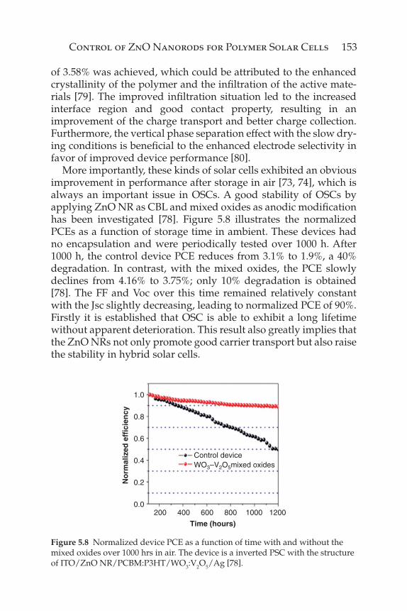
More importantly, these kinds of solar cells exhibited an obvious improvement in performance after storage in air [73, 74], which is always an important issue in OSCs. A good stability of OSCs by applying ZnO NR as CBL and mixed oxides as anodic modification has been investigated [78]. Figure 5.8 illustrates the normalized PCEs as a function of storage time in ambient. These devices had no encapsulation and were periodically tested over 1000 h. After 1000 h, the control device PCE reduces from 3.1% to 1.9%, a 40% degradation. In contrast, with the mixed oxides, the PCE slowly declines from 4.16% to 3.75%; only 10% degradation is obtained [78]. The FF and Voc over this time remained relatively constant with the Jsc slightly decreasing, leading to normalized PCE of 90%. Firstly it is established that OSC is able to exhibit a long lifetime without apparent deterioration. This result also greatly implies that the ZnO NRs not only promote good carrier transport but also raise the stability in hybrid solar cells.
2000.0
0.2
0.4
0.6
0.8
1.0
400 600
Time (hours)
No
rmal
ized
eff
icie
ncy
800 1000 1200
Control deviceWO3–V2O5mixed oxides
Figure 5.8 Normalized device PCE as a function of time with and without the mixed oxides over 1000 hrs in air. The device is a inverted PSC with the structure of ITO/ZnO NR/PCBM:P3HT/WO3:V2O5/Ag [78].

154 Solar Cell Nanotechnology
5.4 Conclusion and Outlook
This chapter provides an overview of the preparation and charac-terization of ZnO NR, as well as the most recent research devel-opments in the application of ZnO NRs in polymer solar cells. Vertically-aligned nanostructures have been exhaustively applied as electron transport material in polymer solar cells. They could introduce a high surface area for higher interface between the light-harvesting materials (polymer) and increase the photon absorp-tion. Over the past few years, outstanding progress has been observed on the synthesis of vertically-aligned ZnO NRs. The good electron transport by applying ZnO NRs is a reality. The current densities have been effectively raised by applying verti-cal nanostructures compared to their planar counterparts. So far, the best solar cell performance by applying ZnO nanostructures in PSCs can achieve an effi ciency of 7.2%. In order to further increase solar cell effi ciency, the surface area of the nanostructured ZnO electrode must be enriched. In an effort to increase surface area and the interface between the semiconductor and the organic material (polymer), a synthesis technique that is able to control the vertically-aligned nanostructures at the 3D level will be in great demand in the future. Therefore, the vertical ZnO nanostructures such as branched nanorods or nanosheets, appear to be promis-ing candidates to carry out high effi ciency polymer solar cells. The ZnO nanostructures, which demonstrate most of the characteristics required for high electron transport and high solar cell effi ciency of high density nanostructure, high surface area, low voids concentra-tion, and single-crystalline structure for electron transport without grain boundaries, will still be a critical material applied in PSCs in the future.
References
1. F. Padinger, R. S. Rittberger and N. S. Sariciftci, Advanced Functional Materials, Vol. 13, p. 85, 2003.
2. G . Li, V. Shrotriya, J. S. Huang, Y. Yao, T. Moriarty, K. Emery and Y. Yang, Nature Materials, Vol. 4, p. 864, 2005.
3. M. Reyse-Reyes, K. Kim and D. L Carroll, Applied Physical Letters, Vol. 87, 083506, 2005.
4. C. Y. Kwong, A. B. Djurisic, P. C. Chui, K. W. Cheng and W. K. Chan, Chemical Physics Letters, Vol. 384, p. 372, 2004.

Control of ZnO Nanorods for Polymer Solar Cells 155
5. P. A. van Hal, M. M. Wienk, J. M. Kroon, W. J. H. Verhees, L. H. Slooff, W. J. H. van Gennip, P. Jonkheijm and R. A. J. Janssen, Advanced Materials, Vol. 15, p. 118, 2003.
6. W. J. E. Beek, M. M. Wienk and R. A. J. Janssen, Advanced Materials, Vol. 16, p. 1009, 2004.
7. W. J. E. Beek, L. H. Slooff, M. M. Wienk, J. M. Kroon and R. A. J. Janssen, Advanced Functional Materials, Vol. 15, p. 1703, 2005.
8. W. U. Huynh, J. J. Dittmer and A. P. Alivisatos, Science, Vol. 295, p. 2425, 2002. 9. S. D. Oosterhout, M. M. Wienk, S. S. van Bavel, R. Thiedmann, L. J. A. Koster,
J. Gilot, J. Loos, V. Schmidt and R. A. J. Janssen, Nature Materials, Vol. 8, p. 818, 2009.10. H. Sirringhaus et al, Nature, Vol. 401, p. 685, 1999.11. K. M. Coakley, Y. X. Liu, M. D. McGehee, K. L. Frindell and G. D. Stucky,
Advanced Functional Materials, Vol. 13, p. 301, 2003.12. K. M. Coakley, B. S. Srinivasan, J. M. Ziebarth, C. Goh, X. Y. Liu and
M. D. McGehee, Advanced Functional Materials, Vol. 15, p. 1927, 2005.13. J. Chen, J. Li, J. Li, G. Xiao and X. Yang, Journal of Alloys and Compounds,
Vol. 509, p. 740, 2010.14. W. K. Tan, K. A. Razak, K. Ibrahim and Z. Lockman, Journal of Alloys and
Compounds, Vol. 509, p. 820, 2010.15. Z. Lockman, Y. P. Fong, T. W. Kian, K. Ibrahim and K. A. Razak, Journal of
Alloys and Compounds, Vol. 493, p. 699, 2010.16. S. Baruah and J. Dutta, Journal of Sol-gel Science and Technology, Vol. 50, p. 456,
2009.17. L. Spanhel, Journal of Sol-gel Science and Technology, Vol. 39, p. 7, 2006.18. X. Ma, H. Zhang, Y. Ji, J. Xu and D. Yang, Materials Letters, Vol. 59, p. 3393,
2005.19. M. Kohls, M. Bonnani and L. Spanhel, Applied Physical Letters, Vol. 81, p. 3858,
2002.20. H. Y. Xu, H. Wang, Y. C. Zhang, S. Wang, M. Zhu and H. Yan, Crystal
Research and Technology, Vol. 38, p. 429, 2003.21. S. Shingubara, Journal of Nanoparticle Research, Vol. 5, p. 17, 2003.22. L. Vayssieres, K. Keis and S. E. Lindquist, Journal of Physical Chemistry B,
Vol. 105, p. 3350, 2001.23. L. Schmidt-Mende and J. L. MacManus-Driscoll, Materials Today, Vol. 10, p. 40,
2007.24. M. N. R. Ashfold, R. P. Doherty, N. G. Ndifor-Angwafor, D. J. Riley and Y. Sun,
Thin Solid Films, Vol. 515, p. 8679, 2007.25. K. Govender, D. S. Boyle, P. B. Kenway and P. O’Brien, Journal of Materials
Chemistry, Vol. 14, p. 2575, 2004.26. A. Sugunan, H. C. Warad,M. Boman and J. Dutta, Journal of Sol-gel Science and
Technology, Vol. 39, p. 49, 2006.27. L. Vayssieres, K. Keis, S. E. Lindquist and A. Hagfeldt, Journal of Physical
Chemistry B, Vol. 105, p. 3350, 2001.28. L. Vayssieres, Advanced Materials, Vol. 15, p. 464, 2003.29. Y. Sun, D. J. Riley and M. N. R. Ashfold, Journal of Physical Chemistry B, Vol. 110,
p. 15186, 2006.30. Z. R. Tian, J. A. Voigt , J. Liu, B. Mckenzie, M. J. Mcdermott, M. A. Rodriguez,
H. Konishi and H. Xu, Nature Materials, Vol. 2, p. 821, 2003.31. U. Pal and P. Santiago, Journal of Physical Chemistry B, Vol. 109, p. 15317, 2005.

156 Solar Cell Nanotechnology
32. L. Tang, X. B. Bao, H. Zhou and A. H. Yuan, Physica E, Vol. 40, p. 924, 2008.33. Li F, Hu L, Li Z and Huang X, Journal of Alloys and Compounds, Vol. 465, p. L14,
2007.34. Y. Chen, R. Yu, Q. Shi, J. Qin and F. Zheng, Materials Letters, Vol. 61, p. 4438,
2007.35. Y. H. Ni, X. W. Wei, X. Ma and J. M. Hong, Journal of Crystal Growth, Vol. 283,
p. 48, 2005.36. Z. Li, X. Huang, J. Liu, Y. Li, X. Ji and G. Li, Materials Letters, Vol. 61, p. 4362,
2007. 37. N. S. Ridhuan, Y. P. Fong, Z. Lockman, K. A. Razak, Applied Mechanics and
Materials, Vol. 83, p.116, 2011.38. X. Zhao, J. Y. Lee, C. R. Kim, J. Heo, C. M. Shin et al., Physica E, Vol. p. 41,
p. 1423, 2009.39. C. M. Shin, J. Y. Lee, J. H. Heo, J. H. Park, C. R. Kim et al., Applied Surface
Science, Vol. 255, p. 8501, 2009.40. X. Q. Zhao, C. R. Kim, J. Y. Lee, C. M. Shin, J. H. Heo et al., Applied Surface
Science, Vol. 255, p. 5861, 2009.41. M. Guo, P. Diao and S. Cai, Journal of Solid State Chemistry, Vol. 178, p. 1864, 2005.42. Q. Li, J. Bian, J. Sun, J. Wang, Y. Luo et al., Applied Surface Science, Vol. 256,
p. 1698, 2010.43. J. Song, S. Baek, J. Lee, S. Lim, Journal of Chemical Technology and Biotechnology,
Vol. 83, p. 345, 2008.44. S. F. Wang, T. Y. Tseng, Y. R. Wang, C. Y. Wang, H. C. Lu et al., International
Journal of Applied Ceramic Technology, Vol. 5, p. 419, 2008.45. N. Liu, G. Fang, W. Zeng, H. Zhou, F. Cheng et al., ACS Applied Materials and
Interfaces, Vol. 2, p. 1973, 2010.46. S. Y. Liu, T. Chen, J. Wan, G. P. Ru, B. Z. Li et al., Applied Physics A, Vol. 94,
p. 775, 2009.47. X. Q. Zhao, C. R. Kim, J. Y. Lee, J. H. Heo, C. M. Shin et al., Applied Surface
Science, Vol. 255, p. 4461, 2009.48. N. S. Ridhuan, K. A. Razak, Z. Lockman and A. A. Aziz, PLoS one, Vol. 7,
e50405, 2012.49. R. B. Peterson, C. L. Fields and B. A. Gregg, Langmuir, Vol. 20, p. 5114, 2004.50. Z. Zhang and J. Mu, Journal of Colloid Interface Science, Vol. 307, p. 79, 2007.51. Z. Li, X. Huang, J. Liu, Y. Li, G. Li, Materials Letters, Vol. 62, p. 1503, 2008.52. X. X. Liu, Z. G. Jin, S. J. Bu, J. Zhao, K. Yu, Materials Science Engineering B,
Vol. 129, p. 139, 2006.53. C. Herring, Structure and Properties of Solid Surfaces, University Chicago Press,
Chicago, IL, 1953.54. D. C. Olson, J. Piris, R. T. Collins, S. E. Shaheen and D. S. Ginley, Thin Solid
Films, Vol. 496, p. 26, 2006.55. D. C. Olson, Y. J. Lee, M. S. White, N. Kopidakis, S. E. Shaheen, D. S. Ginley,
J. A. Voigt and J. W. P. Hsu, Journal of Physical Chemistry C, Vol. 111, p. 16640, 2007.
56. D. Q. Bi, F. Wu, W. J. Yue, Y. Guo, W. Shen, R. X. Peng, H. A. Wu, X. K. Wang and M. T. Wang, Journal of Physical Chemistry C, Vol. 114, p. 13846, 2010.
57. P. Atienzar, T. Ishwara, B. N. Illy, M. P. Ryan, B. C. O’Regan, J. R. Durrant and J. Nelson, Journal of Physical Chemical Letters, Vol. 1, p. 708, 2010.

Control of ZnO Nanorods for Polymer Solar Cells 157
58. D. C. Olson, Y. J. Lee, M. S. White, N. Kopidakis, S. E. Shaheen, D. S. Ginley, J. A. Voigt and J. W. P. Hsu, Journal of Physical Chemistry C, Vol. 112, p. 9544, 2008.
59. Y. Z. Hao, J. Pei, Y. Wei, Y. H. Cao, S. H. Jiao, F. Zhu, J. J. Li and D. H. Xu, Journal of Physical Chemistry C, Vol. 114, p. 8622, 2010.
60. A. M. Peiro, P. Ravirajan, K. Govender, D. S. Boyle, P. O’Brien, D. D. C. Bradley, J. Nelson and J. R. Durrant, Journal of Materials Chemistry, Vol. 16, p. 2088, 2006.
61. Y. Z. Hao, J. Pei, Y. Wei, Y. H. Cao, S. H. Jiao, F. Zhu, J. J. Li and D. H. Xu, Journal of Physical Chemistry C, Vol. 114, p. 8622, 2010.
62. U. Ozgur, Y. I. Alivov, C. Liu, A. Teke, M. A. Reshchikov, S. Dogan, V. Avrutin, S. J. Cho and H. Morkoc, Journal of Applied Physics, Vol. 98, 041301, 2005.
63. W. U. Huynh, J. J. Dittmer and A. P. Alivisatos, Science, Vol. 295, p. 2425, 2002.64. C. Y. Kwong, A. B. Djurisic, P. C. Chui, K. W. Cheng and W. K. Chan, Chemical
Physics Letters, Vol. 384, p. 372, 2004.65. R. Po, C. Carbonera, A. Bernardi and N. Camaioni, Energy Environmental
Science, Vol. 4, p. 285, 2011.66. A. B. Djurisic, A. M. C. Ng and X. Y. Chen, Progress in Quantum Electronics,
Vol. 34, p. 191, 2010.67. S. K. Hau, H. L. Yip and A. K. Y. Jen, Polymer Reviews, Vol. 50, p. 474, 2010.68. U. Ozgur, D. Hofstetter and H. Morkoc, Proceedings of the IEEE, Vol. 98, p. 1255,
2010. 69. M. Jørgensen, K. Norrman and F. C. Krebs, Solar Energy Materials and Solar
Cells, Vol. 92, p. 686, 2008.70. F. C. Krebs and K. Norrman, Progress in Photovoltaics: Research and Applications,
Vol. 15, p. 697, 2007.71. M. P. de Jong, L. J. van Ijzendoorn and M. J. A. de Voigt, Applied Physical Letters,
Vol. 77, p. 2255, 2000.72. M. Jørgensen, K. Norrman, S. A. Gevorgyan, T. Tromholt, B. Anderreasen and
F. C. Krebs, Advanced Materials, Vol. 24, p. 580, 2012.73. G. Li, C. W. Chu, V. Shrotriya, J. Huang and Y. Yang, Applied Physical Letters,
Vol. 88, 253503, 2006.74. M. S. White, D. C. Olson, S. E. Shaheen, N. Kopidakis, D. S. Ginley, Applied
Physical Letters, Vol. 89, 143517, 2006.75. K. Takanezawa, K. Hirota, Q. S. Wei, K. Tajima and K. Hashimoto, Journal of
Physical Chemistry C, Vol. 111, p. 7218, 2007.76. H. C. Liao, C. C. Lin, Y. W. Chen, T. C. Liu and S. Y. Chen, Journal of Materials
Chemistry, Vol. 20, p. 5429, 2010.77. J. S. Huang, C. Y. Chou, M. Y. Liu, K. H. Tsai, W. H. Lin and C. F. Lin, Organic
Electronics, Vol. 10, p. 1060, 2009,78. J. S. Huang, C. Y. Chou and C. F. Lin, IEEE Electron Device Letters, Vol. 31,
p. 332, 2010. 79. C. Y. Chou, J. S. Huang, C. H. Wu, C. Y. Lee and C. F. Lin, Solar Energy Materials
and Solar Cells, Vol. 93, p. 1608, 2009.80. M. Campoy-Quiles, T. Ferenczi, T. Agostinelli, P. G. Etchegoin, Y. Kim,
T. D. Anthopoulos, P. N. Stavrinou, D. D. C. Bradley and J. Nelson, Nature Materials, Vol. 7, p. 158, 2008.