SOJ, TSOP, FP-BGA 128K x 8 1Mb Asynchronous SRAM DD SS · • Industrial Temperature Option:...
16
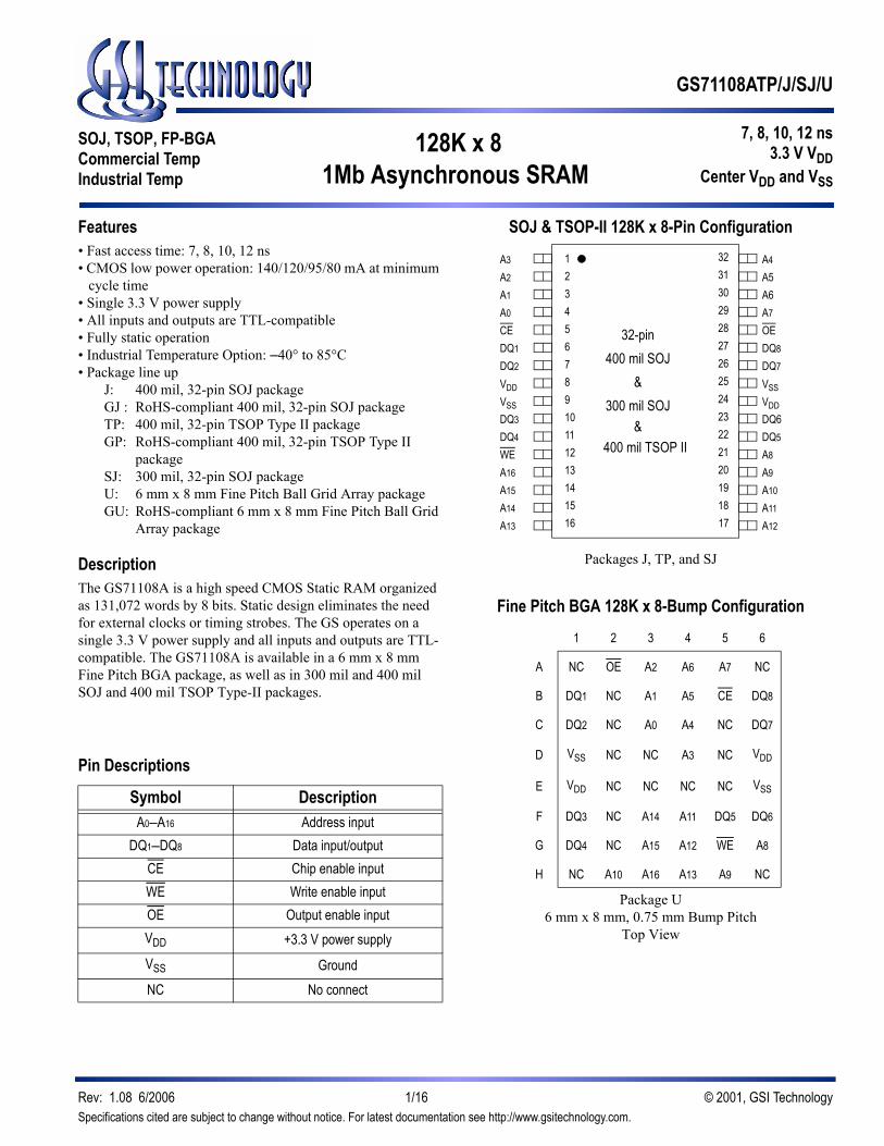
GS71108ATP/J/SJ/U 128K x 8 1Mb Asynchronous SRAM 7, 8, 10, 12 ns 3.3 V V DD Center V DD and V SS SOJ, TSOP, FP-BGA Commercial Temp Industrial Temp Rev: 1.08 6/2006 1/16 © 2001, GSI Technology Specifications cited are subject to change without notice. For latest documentation see http://www.gsitechnology.com. Features • Fast access time: 7, 8, 10, 12 ns • CMOS low power operation: 140/120/95/80 mA at minimum cycle time • Single 3.3 V power supply • All inputs and outputs are TTL-compatible • Fully static operation • Industrial Temperature Option: –40° to 85°C • Package line up J: 400 mil, 32-pin SOJ package GJ : RoHS-compliant 400 mil, 32-pin SOJ package TP: 400 mil, 32-pin TSOP Type II package GP: RoHS-compliant 400 mil, 32-pin TSOP Type II package SJ: 300 mil, 32-pin SOJ package U: 6 mm x 8 mm Fine Pitch Ball Grid Array package GU: RoHS-compliant 6 mm x 8 mm Fine Pitch Ball Grid Array package Description The GS71108A is a high speed CMOS Static RAM organized as 131,072 words by 8 bits. Static design eliminates the need for external clocks or timing strobes. The GS operates on a single 3.3 V power supply and all inputs and outputs are TTL- compatible. The GS71108A is available in a 6 mm x 8 mm Fine Pitch BGA package, as well as in 300 mil and 400 mil SOJ and 400 mil TSOP Type-II packages. Pin Descriptions Symbol Description A0–A16 Address input DQ1–DQ8 Data input/output CE Chip enable input WE Write enable input OE Output enable input V +3.3 V power supply V Ground NC No connect 32 31 30 29 28 27 26 25 24 23 22 21 20 19 18 17 1 2 3 4 5 6 7 8 9 10 11 12 13 14 15 16 A3 A2 A1 A0 CE DQ1 DQ2 V DD V SS DQ3 DQ4 WE A16 A15 A14 A13 A4 A5 A6 A7 OE DQ8 DQ7 V SS V DD DQ6 DQ5 A8 A9 A10 A11 A12 32-pin 400 mil SOJ 300 mil SOJ & & 400 mil TSOP II SOJ & TSOP-II 128K x 8-Pin Configuration Packages J, TP, and SJ 1 2 3 4 5 6 A NC OE A2 A6 A7 NC B DQ1 NC A1 A5 CE DQ8 C DQ2 NC A0 A4 NC DQ7 D V SS NC NC A3 NC V DD E V DD NC NC NC NC V SS F DQ3 NC A14 A11 DQ5 DQ6 G DQ4 NC A15 A12 WE A8 H NC A10 A16 A13 A9 NC Fine Pitch BGA 128K x 8-Bump Configuration Package U 6 mm x 8 mm, 0.75 mm Bump Pitch Top View DD SS
Transcript of SOJ, TSOP, FP-BGA 128K x 8 1Mb Asynchronous SRAM DD SS · • Industrial Temperature Option:...
GS71108ATP/J/SJ/U
128K x 81Mb Asynchronous SRAM
7, 8, 10, 12 ns3.3 V VDD
Center VDD and VSS
SOJ, TSOP, FP-BGACommercial TempIndustrial Temp
Features• Fast access time: 7, 8, 10, 12 ns• CMOS low power operation: 140/120/95/80 mA at minimum
cycle time• Single 3.3 V power supply• All inputs and outputs are TTL-compatible• Fully static operation• Industrial Temperature Option: –40° to 85°C• Package line up
J: 400 mil, 32-pin SOJ packageGJ : RoHS-compliant 400 mil, 32-pin SOJ packageTP: 400 mil, 32-pin TSOP Type II packageGP: RoHS-compliant 400 mil, 32-pin TSOP Type II
packageSJ: 300 mil, 32-pin SOJ packageU: 6 mm x 8 mm Fine Pitch Ball Grid Array packageGU: RoHS-compliant 6 mm x 8 mm Fine Pitch Ball Grid
Array package
DescriptionThe GS71108A is a high speed CMOS Static RAM organized as 131,072 words by 8 bits. Static design eliminates the need for external clocks or timing strobes. The GS operates on a single 3.3 V power supply and all inputs and outputs are TTL-compatible. The GS71108A is available in a 6 mm x 8 mm Fine Pitch BGA package, as well as in 300 mil and 400 mil SOJ and 400 mil TSOP Type-II packages.
Pin Descriptions
Symbol DescriptionA0–A16 Address input
DQ1–DQ8 Data input/outputCE Chip enable inputWE Write enable inputOE Output enable inputV +3.3 V power supplyV GroundNC No connect
32313029282726252423222120191817
12345678910111213141516
A3
A2
A1
A0
CEDQ1
DQ2
VDDVSSDQ3
DQ4
WEA16
A15
A14
A13
A4
A5A6A7
OEDQ8
DQ7
VSSVDDDQ6DQ5
A8
A9
A10
A11
A12
32-pin400 mil SOJ
300 mil SOJ&
&400 mil TSOP II
SOJ & TSOP-II 128K x 8-Pin Configuration
Packages J, TP, and SJ
1 2 3 4 5 6
A NC OE A2 A6 A7 NC
B DQ1 NC A1 A5 CE DQ8
C DQ2 NC A0 A4 NC DQ7
D VSS NC NC A3 NC VDD
E VDD NC NC NC NC VSS
F DQ3 NC A14 A11 DQ5 DQ6
G DQ4 NC A15 A12 WE A8
H NC A10 A16 A13 A9 NC
Fine Pitch BGA 128K x 8-Bump Configuration
Package U6 mm x 8 mm, 0.75 mm Bump Pitch
Top ViewDD
SS
Rev: 1.08 6/2006 1/16 © 2001, GSI TechnologySpecifications cited are subject to change without notice. For latest documentation see http://www.gsitechnology.com.
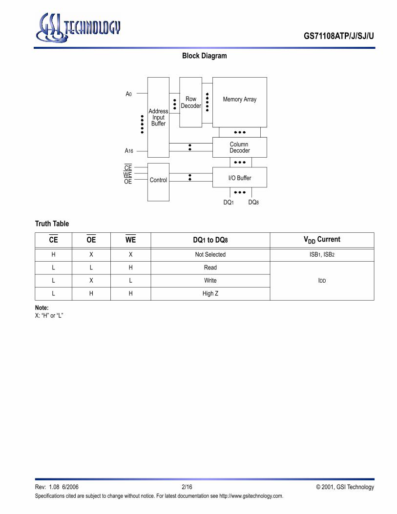
GS71108ATP/J/SJ/U
Memory ArrayRowDecoder
Column Decoder
AddressInputBuffer
Control I/O Buffer
A0
CEWEOE
DQ1
A16
DQ8
Block Diagram
Truth Table
CE OE WE DQ1 to DQ8 VDD Current
H X X Not Selected ISB1, ISB2
L L H Read
IDDL X L Write
L H H High Z
Note: X: “H” or “L”
Specifications cited are subject to change without notice. For latest documentation see http://www.gsitechnology.com.Rev: 1.08 6/2006 2/16 © 2001, GSI Technology

GS71108ATP/J/SJ/U
Absolute Maximum Ratings
Parameter Symbol Rating UnitSupply Voltage VDD –0.5 to +4.6 V
Input Voltage VIN–0.5 to VDD +0.5(≤ 4.6 V max.) V
Output Voltage VOUT–0.5 to VDD +0.5(≤ 4.6 V max.)
V
Allowable power dissipation PD 0.7 W
Storage temperature TSTG –55 to 150 oC
Note: Permanent device damage may occur if Absolute Maximum Ratings are exceeded. Functional operation shall be restricted to Recommended Operating Conditions. Exposure to higher than recommended voltages for extended periods of time could affect device reliability.
Recommended Operating Conditions
Parameter Symbol Min Typ Max Unit
Supply Voltage for -7/-8/-10/-12 VDD 3.0 3.3 3.6 V
Input High Voltage VIH 2.0 — VDD +0.3 V
Input Low Voltage VIL –0.3 — 0.8 V
Ambient Temperature, Commercial Range TAc 0 — 70 oC
Ambient Temperature,Industrial Range TAI –40 — 85 oC
Notes: 1. Input overshoot voltage should be less than VDD +2 V and not exceed 20 ns. 2. Input undershoot voltage should be greater than –2 V and not exceed 20 ns.
Specifications cited are subject to change without notice. For latest documentation see http://www.gsitechnology.com.Rev: 1.08 6/2006 3/16 © 2001, GSI Technology

GS71108ATP/J/SJ/U
Capacitance
Parameter Symbol Test Condition Max UnitInput Capacitance C V = 0 V 5 pF
Output Capacitance C V = 0 V 7 pF
Notes: 1. Tested at TA = 25°C, f = 1 MHz2. These parameters are sampled and are not 100% tested.
DC I/O Pin Characteristics
Parameter Symbol Test Conditions Min MaxInput Leakage
Current IIL VIN = 0 to VDD –1 uA 1 uA
Output Leakage Current ILO
Output High ZVOUT = 0 to VDD
–1 uA 1 uA
Output High Voltage VOH I = –4 mA 2.4 —
Output Low Voltage VOL I = +4 mA — 0.4 V
Power Supply Currents
Parameter Symbol Test Conditions0 to 70°C –40 to 85°C
7 ns 8 ns 10 ns 12 ns 7 ns 8 ns 10 ns 12 ns
OperatingSupplyCurrent
I
CE ≤ VAll other inputs ≥ V or ≤ V
Min. cycle timeI = 0 mA
140 mA 120 mA 95 mA 80 mA 145 mA 125 mA 100 mA 85 mA
StandbyCurrent I
CE ≥ V All other inputs≥ V or ≤V
Min. cycle time
25 mA 20 mA 20 mA 15 mA 30 mA 25 mA 25 mA 20 mA
StandbyCurrent I
CE ≥ V – 0.2 VAll other inputs
≥ V – 0.2 V or ≤ 0.2 V2 mA 5 mA
IN IN
OUT OUT
OH
LO
DD
IL
IH IL
OUT
SB1
IH
IH IL
SB2DD
DD
Specifications cited are subject to change without notice. For latest documentation see http://www.gsitechnology.com.Rev: 1.08 6/2006 4/16 © 2001, GSI Technology

GS71108ATP/J/SJ/U
DQ
VT = 1.4 V
50Ω 30pF1
DQ
3.3 V
Output Load 1
Output Load 2
589Ω
434Ω5pF1Notes:1. Include scope and jig capacitance.2. Test conditions as specified with output loading as shown in Fig. 1
unless otherwise noted.3. Output load 2 for tLZ, tHZ, tOLZ and tOHZ
Parameter ConditionsInput high level VIH = 2.4 V
Input low level VIL = 0.4 V
Input rise time tr = 1 V/ns
Input fall time tf = 1 V/ns
Input reference level 1.4 V
Output reference level 1.4 V
Output load Fig. 1& 2
AC Test Conditions
AC Characteristics
Read Cycle
Parameter Symbol-7 -8 -10 -12
UnitMin Max Min Max Min Max Min Max
Read cycle time t 7 — 8 — 10 — 12 — ns
Address access time t — 7 — 8 — 10 — 12 ns
Chip enable access time (CE) t — 7 — 8 — 10 — 12 ns
Output enable to output valid (OE) t — 3 — 3.5 — 4 — 5 ns
Output hold from address change t 3 — 3 — 3 — 3 — ns
Chip enable to output in low Z (CE) t * 3 — 3 — 3 — 3 — ns
Output enable to output in low Z (OE) t * 0 — 0 — 0 — 0 — ns
Chip disable to output in High Z (CE) t * — 3.5 — 4 — 5 — 6 ns
Output disable to output in High Z (OE) t * — 3 — 3.5 — 4 — 5 ns
* These parameters are sampled and are not 100% tested
RC
AA
AC
OE
OH
LZ
OLZ
HZ
OHZ
Specifications cited are subject to change without notice. For latest documentation see http://www.gsitechnology.com.Rev: 1.08 6/2006 5/16 © 2001, GSI Technology

GS71108ATP/J/SJ/U
tAA
tOH
tRC
Address
Data Out Previous Data Data valid
Read Cycle 1: CE = OE = VIL, WE = VIH
tAA
tRC
Address
tAC
tLZ
tOE
tOLZ
CE
OE
Data Out
tHZ
tOHZ
DATA VALID
High impedance
Read Cycle 2: WE = VIH
Specifications cited are subject to change without notice. For latest documentation see http://www.gsitechnology.com.Rev: 1.08 6/2006 6/16 © 2001, GSI Technology

GS71108ATP/J/SJ/U
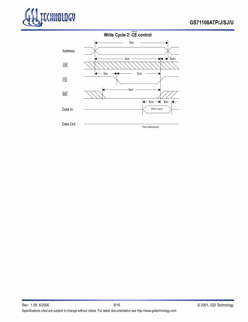
Write Cycle
Parameter Symbol-7 -8 -10 -12
UnitMin Max Min Max Min Max Min Max
Write cycle time tWC 7 — 8 — 10 — 12 — ns
Address valid to end of write tAW 5 — 5.5 — 7 — 8 — ns
Chip enable to end of write tCW 5 — 5.5 — 7 — 8 — ns
Data set up time tDW 3 — 4 — 5 — 6 — ns
Data hold time tDH 0 — 0 — 0 — 0 — ns
Write pulse width tWP 5 — 5.5 — 7 — 8 — ns
Address set up time tAS 0 — 0 — 0 — 0 — ns
Write recovery time (WE) tWR 0 — 0 — 0 — 0 — ns
Write recovery time (CE) tWR1 0 — 0 — 0 — 0 — ns
Output Low Z from end of write tWLZ* 3 — 3 — 3 — 3 — ns
Write to output in High Z tWHZ* — 3 — 3.5 — 4 — 5 ns
* These parameters are sampled and are not 100% tested
tWC
Address
CE
WE
Data In
OE
Data Out
tAW
tCW
tAS tWP
tWR
tDW tDH
tWLZtWHZ
DATA VALID
HIGH IMPEDANCE
Write Cycle 1: WE control
Specifications cited are subject to change without notice. For latest documentation see http://www.gsitechnology.com.Rev: 1.08 6/2006 7/16 © 2001, GSI Technology
GS71108ATP/J/SJ/U
tWC
Address
CE
WE
Data In
OE
Data Out
tAW
tWP
tAS tCW
tWR1
tDW tDH
DATA VALID
HIGH IMPEDANCE
Write Cycle 2: CE control
Specifications cited are subject to change without notice. For latest documentation see http://www.gsitechnology.com.Rev: 1.08 6/2006 8/16 © 2001, GSI Technology
GS71108ATP/J/SJ/U
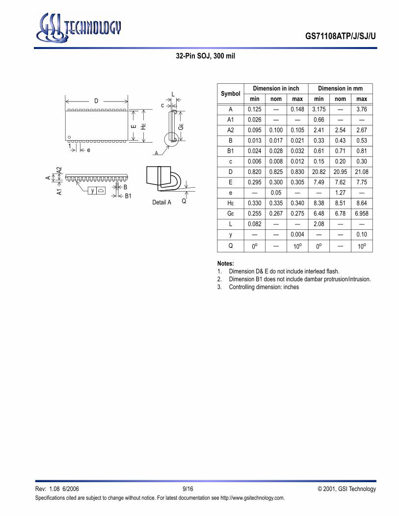
1 e
B1
D
A1A2
y
E HE
Q
cL
GE
Detail A
A
B
A
Notes:1. Dimension D& E do not include interlead flash.2. Dimension B1 does not include dambar protrusion/intrusion.3. Controlling dimension: inches
SymbolDimension in inch Dimension in mm
min nom max min nom maxA 0.125 — 0.148 3.175 — 3.76
A1 0.026 — — 0.66 — —A2 0.095 0.100 0.105 2.41 2.54 2.67B 0.013 0.017 0.021 0.33 0.43 0.53
B1 0.024 0.028 0.032 0.61 0.71 0.81c 0.006 0.008 0.012 0.15 0.20 0.30D 0.820 0.825 0.830 20.82 20.95 21.08E 0.295 0.300 0.305 7.49 7.62 7.75e — 0.05 — — 1.27 —
HE 0.330 0.335 0.340 8.38 8.51 8.64GE 0.255 0.267 0.275 6.48 6.78 6.958L 0.082 — — 2.08 — —y — — 0.004 — — 0.10Q 0o — 10o 0o — 10o
32-Pin SOJ, 300 mil
Specifications cited are subject to change without notice. For latest documentation see http://www.gsitechnology.com.Rev: 1.08 6/2006 9/16 © 2001, GSI Technology

GS71108ATP/J/SJ/U
1 e
B1
D
A1A2
y
E HE
Q
cL
GE
Detail A
A
B
A
Notes:1. Dimension D& E do not include interlead flash.2. Dimension B1 does not include dambar protrusion/intrusion.3. Controlling dimension: inches
SymbolDimension in inch Dimension in mm
min nom max min nom maxA — — 0.146 — — 3.70
A1 0.026 — — 0.66 — —A2 0.105 0.110 0.115 2.67 2.80 2.92B 0.013 0.017 0.021 0.33 0.43 0.53
B1 0.024 0.028 0.032 0.61 0.71 0.81c 0.006 0.008 0.012 0.15 0.20 0.30D 0.820 0.824 0.829 20.83 20.93 21.06E 0.395 0.400 0.405 10.04 10.16 10.28e — 0.05 — — 1.27 —
HE 0.430 0.435 0.440 10.93 11.05 11.17GE 0.354 0.366 0.378 9.00 9.30 9.60L 0.082 — — 2.08 — —y — — 0.004 — — 0.10Q 0o — 10o 0o — 10o
32-Pin SOJ, 400 mil
Specifications cited are subject to change without notice. For latest documentation see http://www.gsitechnology.com.Rev: 1.08 6/2006 10/16 © 2001, GSI Technology

GS71108ATP/J/SJ/U
D
1
32
e b
Q
A
A1A2
y
c
Detail A
E1 E
L
A
ZD
L1
Notes:1. Dimension D includes mold flash, protrusions or gate burrs.2. Dimension E does not include interlead flash3. Controlling dimension: mm
SymbolDimension in inch Dimension in mm
min nom max min nom maxA 0.039 — 0.05 — — 1.27
A1 0.002 — 0.006 0.01 — 0.15A2 0.037 0.040 0.045 0.90 1.02 1.14b 0.012 0.016 0.018 0.30 0.40 0.45c 0.0047 0.0051 0.0062 0.12 0.13 0.16D 0.820 0.825 0.830 20.82 20.95 21.08
ZD — 0.037 — — 0.95 —E 0.455 0.463 0.471 11.56 11.76 11.96
E1 0.395 0.400 0.405 10.03 10.16 10.29e — 0.05 — — 1.27 —L 0.017 0.020 0.023 0.40 0.50 0.60
L1 0.024 0.031 0.039 0.60 0.80 1.00y 0.00 — 0.003 0.00 — 0.76Q 0o — 5o 0o — 5o
32-Pin TSOP-II, 400mil
Specifications cited are subject to change without notice. For latest documentation see http://www.gsitechnology.com.Rev: 1.08 6/2006 11/16 © 2001, GSI Technology
GS71108ATP/J/SJ/U
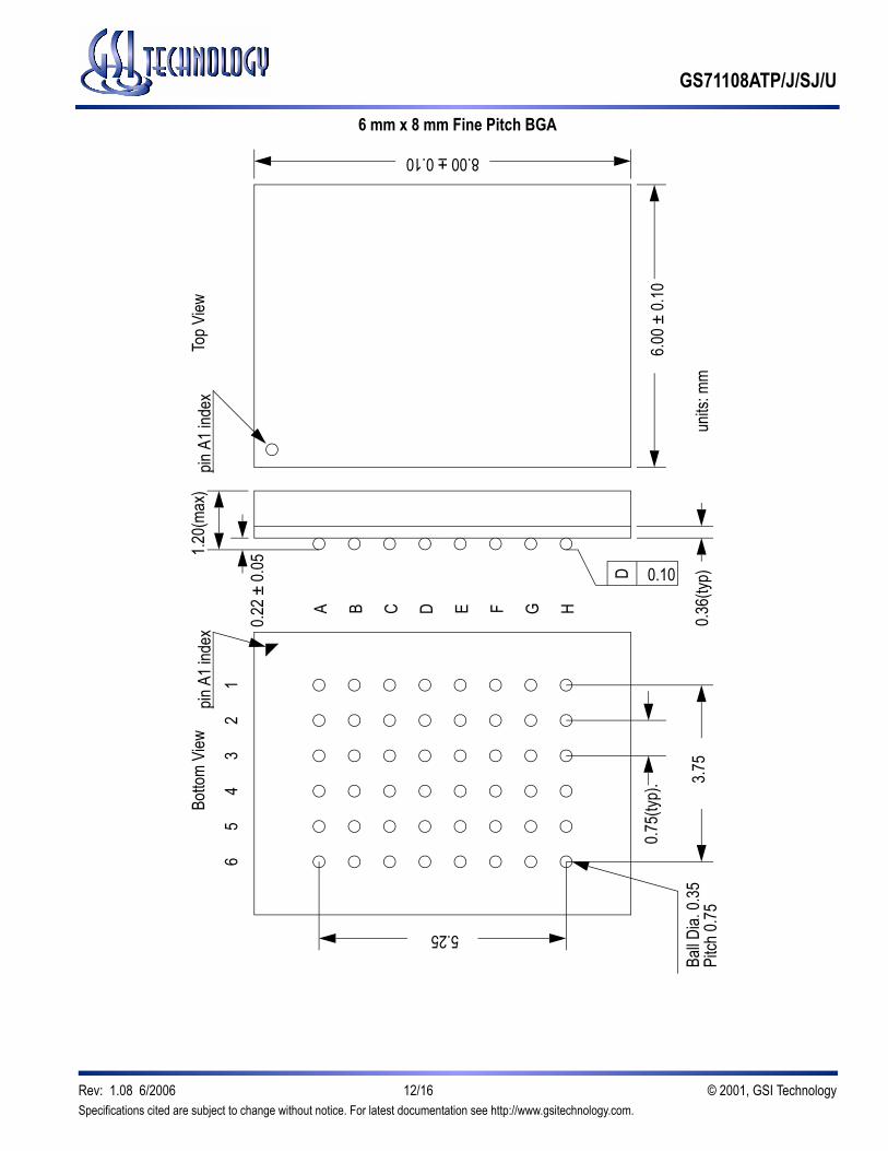
C
5.25
0.75(
typ). 3.7
5
pin A
1 ind
ex6
54
32
1
A B D E F G H
0.22 ±
0.05
1.20(
max)
0.36(
typ)
Ball D
ia. 0.
35Pi
tch 0.
75
D 0.10
pin A
1 ind
exBo
ttom
View
Top V
iew
6.00 ±
0.10
8.00 ± 0.10
units
: mm
6 mm x 8 mm Fine Pitch BGA
Specifications cited are subject to change without notice. For latest documentation see http://www.gsitechnology.com.Rev: 1.08 6/2006 12/16 © 2001, GSI Technology

GS71108ATP/J/SJ/U
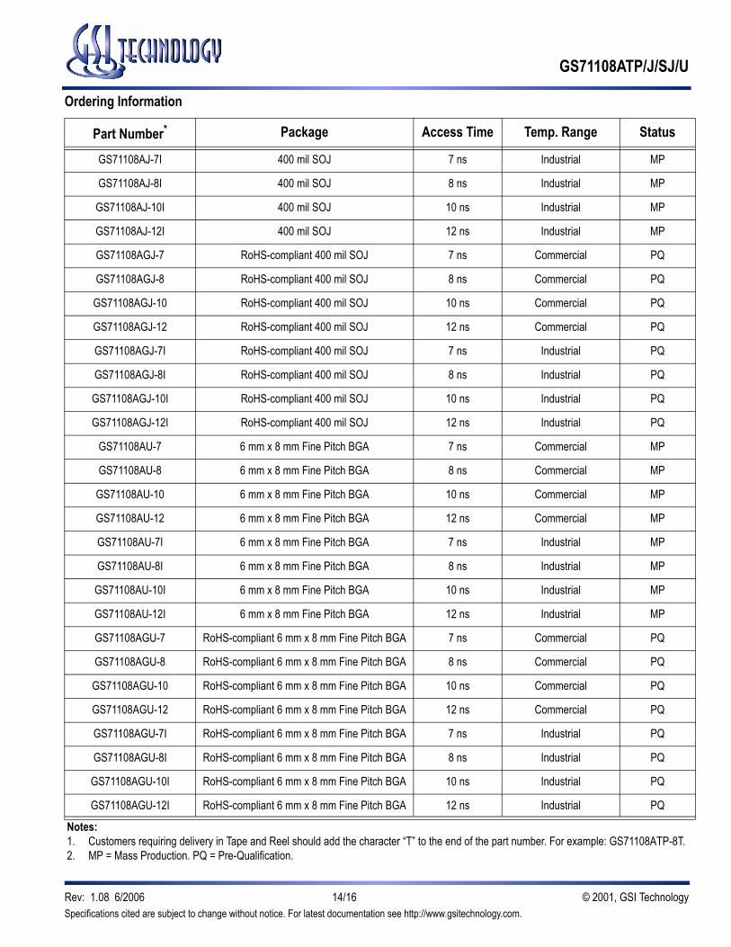
Ordering Information
Part Number* Package Access Time Temp. Range Status
GS71108ATP-7 400 mil TSOP-II 7 ns Commercial MP
GS71108ATP-8 400 mil TSOP-II 8 ns Commercial MP
GS71108ATP-10 400 mil TSOP-II 10 ns Commercial MP
GS71108ATP-12 400 mil TSOP-II 12 ns Commercial MP
GS71108ATP-7I 400 mil TSOP-II 7 ns Industrial MP
GS71108ATP-8I 400 mil TSOP-II 8 ns Industrial MP
GS71108ATP-10I 400 mil TSOP-II 10 ns Industrial MP
GS71108ATP-12I 400 mil TSOP-II 12 ns Industrial MP
GS71108AGP-7 RoHS-compliant 400 mil TSOP-II 7 ns Commercial PQ
GS71108AGP-8 RoHS-compliant 400 mil TSOP-II 8 ns Commercial PQ
GS71108AGP-10 RoHS-compliant 400 mil TSOP-II 10 ns Commercial PQ
GS71108AGP-12 RoHS-compliant 400 mil TSOP-II 12 ns Commercial PQ
GS71108AGP-7I RoHS-compliant 400 mil TSOP-II 7 ns Industrial PQ
GS71108AGP-8I RoHS-compliant 400 mil TSOP-II 8 ns Industrial PQ
GS71108AGP-10I RoHS-compliant 400 mil TSOP-II 10 ns Industrial PQ
GS71108AGP-12I RoHS-compliant 400 mil TSOP-II 12 ns Industrial PQ
GS71108ASJ-7 300 mil SOJ 7 ns Commercial MP
GS71108ASJ-8 300 mil SOJ 8 ns Commercial MP
GS71108ASJ-10 300 mil SOJ 10 ns Commercial MP
GS71108ASJ-12 300 mil SOJ 12 ns Commercial MP
GS71108ASJ-7I 300 mil SOJ 7 ns Industrial MP
GS71108ASJ-8I 300 mil SOJ 8 ns Industrial MP
GS71108ASJ-10I 300 mil SOJ 10 ns Industrial MP
GS71108ASJ-12I 300 mil SOJ 12 ns Industrial MP
GS71108AJ-7 400 mil SOJ 7 ns Commercial MP
GS71108AJ-8 400 mil SOJ 8 ns Commercial MP
GS71108AJ-10 400 mil SOJ 10 ns Commercial MP
GS71108AJ-12 400 mil SOJ 12 ns Commercial MP
Notes:1. Customers requiring delivery in Tape and Reel should add the character “T” to the end of the part number. For example: GS71108ATP-8T.2. MP = Mass Production. PQ = Pre-Qualification.
Specifications cited are subject to change without notice. For latest documentation see http://www.gsitechnology.com.Rev: 1.08 6/2006 13/16 © 2001, GSI Technology
GS71108ATP/J/SJ/U
GS71108AJ-7I 400 mil SOJ 7 ns Industrial MP
GS71108AJ-8I 400 mil SOJ 8 ns Industrial MP
GS71108AJ-10I 400 mil SOJ 10 ns Industrial MP
GS71108AJ-12I 400 mil SOJ 12 ns Industrial MP
GS71108AGJ-7 RoHS-compliant 400 mil SOJ 7 ns Commercial PQ
GS71108AGJ-8 RoHS-compliant 400 mil SOJ 8 ns Commercial PQ
GS71108AGJ-10 RoHS-compliant 400 mil SOJ 10 ns Commercial PQ
GS71108AGJ-12 RoHS-compliant 400 mil SOJ 12 ns Commercial PQ
GS71108AGJ-7I RoHS-compliant 400 mil SOJ 7 ns Industrial PQ
GS71108AGJ-8I RoHS-compliant 400 mil SOJ 8 ns Industrial PQ
GS71108AGJ-10I RoHS-compliant 400 mil SOJ 10 ns Industrial PQ
GS71108AGJ-12I RoHS-compliant 400 mil SOJ 12 ns Industrial PQ
GS71108AU-7 6 mm x 8 mm Fine Pitch BGA 7 ns Commercial MP
GS71108AU-8 6 mm x 8 mm Fine Pitch BGA 8 ns Commercial MP
GS71108AU-10 6 mm x 8 mm Fine Pitch BGA 10 ns Commercial MP
GS71108AU-12 6 mm x 8 mm Fine Pitch BGA 12 ns Commercial MP
GS71108AU-7I 6 mm x 8 mm Fine Pitch BGA 7 ns Industrial MP
GS71108AU-8I 6 mm x 8 mm Fine Pitch BGA 8 ns Industrial MP
GS71108AU-10I 6 mm x 8 mm Fine Pitch BGA 10 ns Industrial MP
GS71108AU-12I 6 mm x 8 mm Fine Pitch BGA 12 ns Industrial MP
GS71108AGU-7 RoHS-compliant 6 mm x 8 mm Fine Pitch BGA 7 ns Commercial PQ
GS71108AGU-8 RoHS-compliant 6 mm x 8 mm Fine Pitch BGA 8 ns Commercial PQ
GS71108AGU-10 RoHS-compliant 6 mm x 8 mm Fine Pitch BGA 10 ns Commercial PQ
GS71108AGU-12 RoHS-compliant 6 mm x 8 mm Fine Pitch BGA 12 ns Commercial PQ
GS71108AGU-7I RoHS-compliant 6 mm x 8 mm Fine Pitch BGA 7 ns Industrial PQ
GS71108AGU-8I RoHS-compliant 6 mm x 8 mm Fine Pitch BGA 8 ns Industrial PQ
GS71108AGU-10I RoHS-compliant 6 mm x 8 mm Fine Pitch BGA 10 ns Industrial PQ
GS71108AGU-12I RoHS-compliant 6 mm x 8 mm Fine Pitch BGA 12 ns Industrial PQ
Ordering Information
Part Number* Package Access Time Temp. Range Status
Notes:1. Customers requiring delivery in Tape and Reel should add the character “T” to the end of the part number. For example: GS71108ATP-8T.2. MP = Mass Production. PQ = Pre-Qualification.
Specifications cited are subject to change without notice. For latest documentation see http://www.gsitechnology.com.Rev: 1.08 6/2006 14/16 © 2001, GSI Technology

GS71108ATP/J/SJ/U
Specifications cited are subject to change without notice. For latest documentation see http://www.gsitechnology.com.Rev: 1.08 6/2006 15/16 © 2001, GSI Technology
GS71108ATP/J/SJ/U
1Mb Asynchronous Datasheet Revision History
Rev. Code: Old;New
Types of ChangesFormat or Content Page #/Revisions/Reason
71108A_r1 • Creation of new datasheet
71108A_r1; 71108A_r1_01 Content • Added 6 ns speed bin to entire document
71108A_r1_01; 71108A _r1_02 Content • Updated all power numbers• Changed 6 mm x 10 mm package designator from U to X
71108A_r1_02; 71108A _r1_03 Content• Updated Recommended Operating Conditions table on page 3• Updated Power Supply Currents table• Changed FPBGA package from 6 x 10 to 6 x 8 (package U)
71108A_r1_03; 71108A _r1_04 Content • Removed 6 ns speed bin from entire document• Added 7 ns speed bin to entire document
71108A_r1_04; 71108A _r1_05 Content • Added missing 300 mil SOJ mechanical drawing
71108A_r1_05; 71108A _r1_06 Content • Updated format• Added RoHS-compliant information for TSOP-II package
71108A_r1_06; 71108A _r1_07 Content • Added RoHS-compliant information for FP-BGA package
71108A_r1_07; 71108A _r1_08 Content • Added RoHS-compliant 400 mil, 32-pin SOJ
Specifications cited are subject to change without notice. For latest documentation see http://www.gsitechnology.com.Rev: 1.08 6/2006 16/16 © 2001, GSI Technology