Software Defined Radio Handbook · Software Defined Radio Handbook Preface SDR (Software Defined...
53
Pentek, Inc. • One Park Way, Upper Saddle River, NJ 07458 • Tel: (201) 818-5900 • Fax: (201) 818-5904 • Email: [email protected] • http://www.pentek.com 1 Software Defined Radio Handbook Eighth Edition Pentek, Inc. One Park Way, Upper Saddle River, New Jersey 07458 Tel: (201) 818-5900 • Fax: (201) 818-5904 Email: [email protected] • http://www.pentek.com Copyright © 1998, 2001, 2003, 2006, 2008, 2009, 2010 Pentek Inc. Last updated: January 2010 All rights reserved. Contents of this publication may not be reproduced in any form without written permission. Specifications are subject to change without notice. Pentek, GateFlow, ReadyFow and VIM are registered trademarks of Pentek, Inc. Sampling Principles of SDR Technology Products Applications Summary Links by Rodger H. Hosking Vice-President & Cofounder of Pentek, Inc. ®
Transcript of Software Defined Radio Handbook · Software Defined Radio Handbook Preface SDR (Software Defined...
Pentek, Inc. • One Park Way, Upper Saddle River, NJ 07458 • Tel: (201) 818-5900 • Fax: (201) 818-5904 • Email: [email protected] • http://www.pentek.com
1
Software Defined Radio Handbook
Eighth Edition
Pentek, Inc.One Park Way, Upper Saddle River, New Jersey 07458
Tel: (201) 818-5900 • Fax: (201) 818-5904
Email: [email protected] • http://www.pentek.com
Copyright © 1998, 2001, 2003, 2006, 2008, 2009, 2010 Pentek Inc.
Last updated: January 2010
All rights reserved.
Contents of this publication may not be reproduced in any form without written permission.
Specifications are subject to change without notice.
Pentek, GateFlow, ReadyFow and VIM are registered trademarks of Pentek, Inc.
Sampling
Principles of SDR
Technology
Products
Applications
Summary
Links
by
Rodger H. HoskingVice-President & Cofounder of Pentek, Inc.
®

Pentek, Inc. • One Park Way, Upper Saddle River, NJ 07458 • Tel: (201) 818-5900 • Fax: (201) 818-5904 • Email: [email protected] • http://www.pentek.com
2
Software Defined Radio Handbook
Preface
SDR (Software Defined Radio) has revolutionized electronic systems for avariety of applications including communications, data acquisition and signal processing.
This handbook shows how DDCs (Digital Downconverters) and DUCs (Digital Upconverters),the fundamental building blocks of SDR, can replace conventional analog receiver designs,
offering significant benefits in performance, density and cost.
In order to fully appreciate the benefits of SDR, a conventional analog receiversystem will be compared to its digital receiver counterpart, highlighting similarities and differences.
The inner workings of the SDR will be explored with an in-depth description of the internalstructure and the devices used. Finally, some actual board- and system-level implementations and available
off-the-shelf SDR products for embedded systems will be described.

Pentek, Inc. • One Park Way, Upper Saddle River, NJ 07458 • Tel: (201) 818-5900 • Fax: (201) 818-5904 • Email: [email protected] • http://www.pentek.com
3
Software Defined Radio Handbook
Before we look at SDR and its various implementa-tions in embedded systems, we’ll review a theoremfundamental to sampled data systems such as thoseencountered in software defined radios.
Nyquist’s Theorem:
“Any signal can be represented by discretesamples if the sampling frequency is at least twice
the bandwidth of the signal.”
Notice that we highlighted the word bandwidthrather than frequency. In what follows, we’ll attempt toshow the implications of this theorem and the correctinterpretation of sampling frequency, also known assampling rate.
Sampling
A Simple Technique to Visualize Sampling
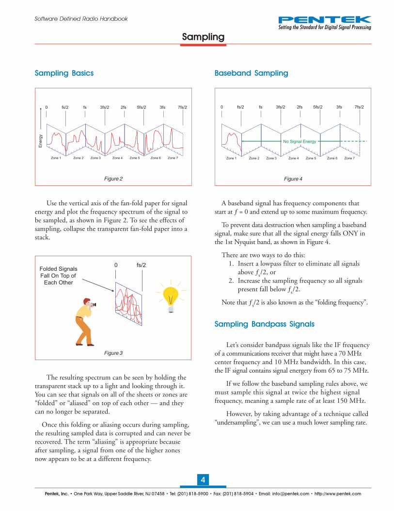
To visualize what happens in sampling, imaginethat you are using transparent “fan-fold” computerpaper. Use the horizontal edge of the paper as thefrequency axis and scale it so that the paper folds lineup with integer multiples of one-half of the samplingfrequency ƒs. Each sheet of paper now represent what wewill call a “Nyquist Zone”, as shown in Figure 1.
Figure 1
Nyquist’s Theorem and Sampling
fs/2 fs 3fs/2 2fs 5fs/2 3fs 7fs/20
Zone 1 Zone 2 Zone 3 Zone 4 Zone 5 Zone 6 Zone 7
Frequency
Pentek, Inc. • One Park Way, Upper Saddle River, NJ 07458 • Tel: (201) 818-5900 • Fax: (201) 818-5904 • Email: [email protected] • http://www.pentek.com
4
Software Defined Radio Handbook
Sampling
Figure 3
Baseband Sampling
Figure 4
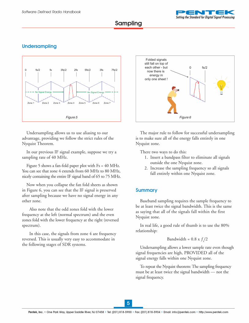
A baseband signal has frequency components thatstart at ƒ = 0 and extend up to some maximum frequency.
To prevent data destruction when sampling a basebandsignal, make sure that all the signal energy falls ONY inthe 1st Nyquist band, as shown in Figure 4.
There are two ways to do this:1. Insert a lowpass filter to eliminate all signals
above ƒs/2, or2. Increase the sampling frequency so all signals
present fall below ƒs/2.
Note that ƒs/2 is also known as the “folding frequency”.
Sampling Bandpass Signals
Figure 2
Use the vertical axis of the fan-fold paper for signalenergy and plot the frequency spectrum of the signal tobe sampled, as shown in Figure 2. To see the effects ofsampling, collapse the transparent fan-fold paper into astack.
Sampling Basics
The resulting spectrum can be seen by holding thetransparent stack up to a light and looking through it.You can see that signals on all of the sheets or zones are“folded” or “aliased” on top of each other — and theycan no longer be separated.
Once this folding or aliasing occurs during sampling,the resulting sampled data is corrupted and can never berecovered. The term “aliasing” is appropriate becauseafter sampling, a signal from one of the higher zonesnow appears to be at a different frequency.
Let’s consider bandpass signals like the IF frequencyof a communications receiver that might have a 70 MHzcenter frequency and 10 MHz bandwidth. In this case,the IF signal contains signal energery from 65 to 75 MHz.
If we follow the baseband sampling rules above, wemust sample this signal at twice the highest signalfrequency, meaning a sample rate of at least 150 MHz.
However, by taking advantage of a technique called“undersampling”, we can use a much lower sampling rate.
fs/2 fs 3fs/2 2fs 5fs/2 3fs 7fs/20
Zone 1 Zone 2 Zone 3 Zone 4 Zone 5 Zone 6 Zone 7
En
erg
y
fs/2 fs 3fs/2 2fs 5fs/2 3fs 7fs/20
Zone 1 Zone 2 Zone 3 Zone 4 Zone 5 Zone 6 Zone 7
No Signal Energy
fs/20Folded Signals
Fall On Top of
Each Other
Pentek, Inc. • One Park Way, Upper Saddle River, NJ 07458 • Tel: (201) 818-5900 • Fax: (201) 818-5904 • Email: [email protected] • http://www.pentek.com
5
Software Defined Radio Handbook
fs/20
Folded signals
still fall on top of
each other - but
now there is
energy in
only one sheet !
Undersampling
Figure 5
Sampling
Figure 6
fs/2 fs 3fs/2 2fs 5fs/2 3fs 7fs/20
Zone 1 Zone 2 Zone 3 Zone 4 Zone 5 Zone 6 Zone 7
No Signal EnergyNo Signal Energy
Undersampling allows us to use aliasing to ouradvantage, providing we follow the strict rules of theNyquist Theorem.
In our previous IF signal example, suppose we try asampling rate of 40 MHz.
Figure 5 shows a fan-fold paper plot with Fs = 40 MHz.You can see that zone 4 extends from 60 MHz to 80 MHz,nicely containing the entire IF signal band of 65 to 75 MHz.
Now when you collapse the fan fold sheets as shownin Figure 6, you can see that the IF signal is preservedafter sampling because we have no signal energy in anyother zone.
Also note that the odd zones fold with the lowerfrequency at the left (normal spectrum) and the evenzones fold with the lower frequency at the right (reversedspectrum).
In this case, the signals from zone 4 are frequencyreversed. This is usually very easy to accommodate inthe following stages of SDR systems.
Summary
Baseband sampling requires the sample frequency tobe at least twice the signal bandwidth. This is the sameas saying that all of the signals fall within the firstNyquist zone.
In real life, a good rule of thumb is to use the 80%relationship:
Bandwidth = 0.8 x ƒs/2
Undersampling allows a lower sample rate even thoughsignal frequencies are high, PROVIDED all of thesignal energy falls within one Nyquist zone.
To repeat the Nyquist theorem: The sampling frequencymust be at least twice the signal bandwidth — not thesignal frequency.
The major rule to follow for successful undersamplingis to make sure all of the energy falls entirely in oneNyquist zone.
There two ways to do this:1. Insert a bandpass filter to eliminate all signals
outside the one Nyquist zone.2. Increase the sampling frequency so all signals
fall entirely within one Nyquist zone.
Pentek, Inc. • One Park Way, Upper Saddle River, NJ 07458 • Tel: (201) 818-5900 • Fax: (201) 818-5904 • Email: [email protected] • http://www.pentek.com
6
Software Defined Radio Handbook
Figure 7
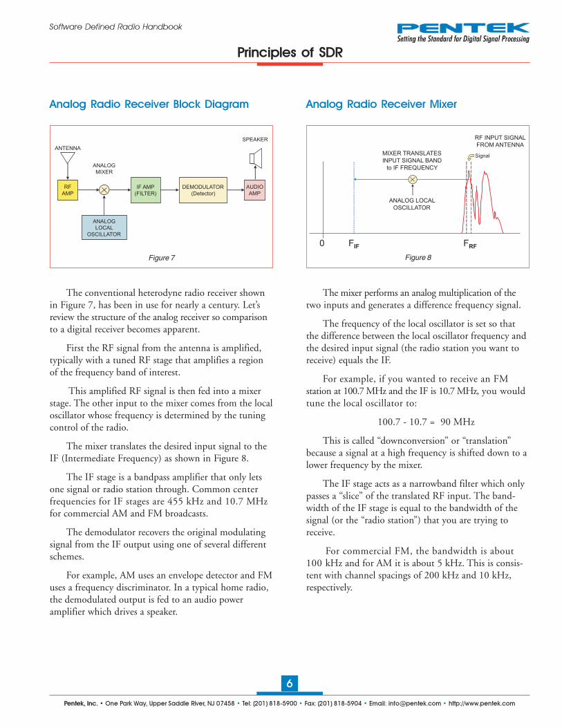
The conventional heterodyne radio receiver shownin Figure 7, has been in use for nearly a century. Let’sreview the structure of the analog receiver so comparisonto a digital receiver becomes apparent.
First the RF signal from the antenna is amplified,typically with a tuned RF stage that amplifies a regionof the frequency band of interest.
This amplified RF signal is then fed into a mixerstage. The other input to the mixer comes from the localoscillator whose frequency is determined by the tuningcontrol of the radio.
The mixer translates the desired input signal to theIF (Intermediate Frequency) as shown in Figure 8.
The IF stage is a bandpass amplifier that only letsone signal or radio station through. Common centerfrequencies for IF stages are 455 kHz and 10.7 MHzfor commercial AM and FM broadcasts.
The demodulator recovers the original modulatingsignal from the IF output using one of several differentschemes.
For example, AM uses an envelope detector and FMuses a frequency discriminator. In a typical home radio,the demodulated output is fed to an audio poweramplifier which drives a speaker.
Figure 8
Analog Radio Receiver Block Diagram Analog Radio Receiver Mixer
The mixer performs an analog multiplication of thetwo inputs and generates a difference frequency signal.
The frequency of the local oscillator is set so thatthe difference between the local oscillator frequency andthe desired input signal (the radio station you want toreceive) equals the IF.
For example, if you wanted to receive an FMstation at 100.7 MHz and the IF is 10.7 MHz, you wouldtune the local oscillator to:
100.7 - 10.7 = 90 MHz
This is called “downconversion” or “translation”because a signal at a high frequency is shifted down to alower frequency by the mixer.
The IF stage acts as a narrowband filter which onlypasses a “slice” of the translated RF input. The band-width of the IF stage is equal to the bandwidth of thesignal (or the “radio station”) that you are trying toreceive.
For commercial FM, the bandwidth is about100 kHz and for AM it is about 5 kHz. This is consis-tent with channel spacings of 200 kHz and 10 kHz,respectively.
Principles of SDR
ANALOG
LOCAL
OSCILLATOR
IF AMP
(FILTER)
SPEAKER
ANTENNA
DEMODULATOR
(Detector)
ANALOG
MIXER
AUDIO
AMP
RF
AMP
0
RF INPUT SIGNAL
FROM ANTENNA
MIXER TRANSLATES
INPUT SIGNAL BAND
to IF FREQUENCY
ANALOG LOCAL
OSCILLATOR
FRFFIF
Signal
Pentek, Inc. • One Park Way, Upper Saddle River, NJ 07458 • Tel: (201) 818-5900 • Fax: (201) 818-5904 • Email: [email protected] • http://www.pentek.com
7
Software Defined Radio Handbook
0 FSIG
MIXER TRANSLATES
INPUT SIGNAL
BAND to DC
DIGITAL LOCAL
OSCILLATOR
FLO = FSIG
CHANNEL
BANDWIDTH
IF BWSignal
DIGITAL
MIXER
DIGITAL
LOCAL
OSC
DSP
DDC
Digital Downconverter
RF
TUNER
Analog
IF Signal
Analog
RF SignalA/D
CONV
Digital IF
Samples LOWPASS
FILTER
Digital
Baseband
Samples
SDR Receiver Block Diagram
Figure 9
Principles of SDR
Figure 10
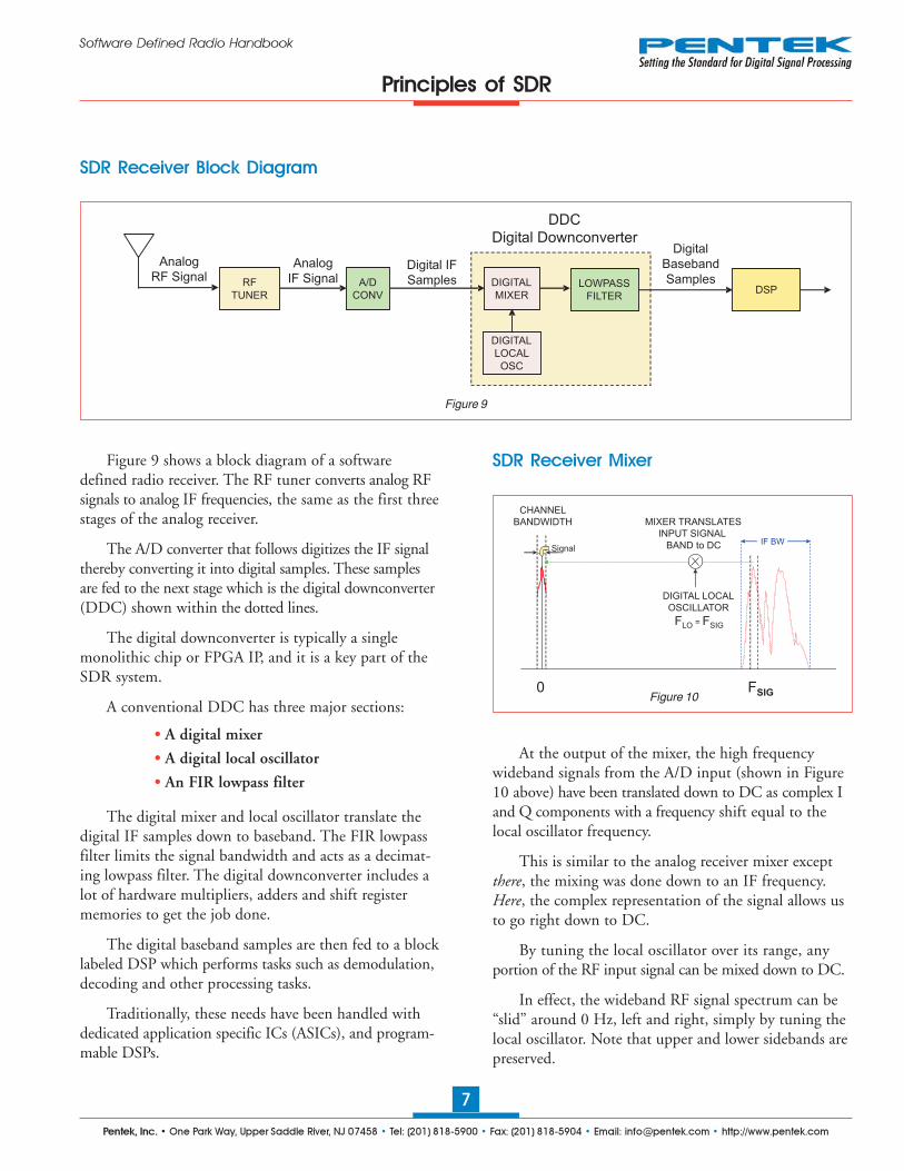
SDR Receiver MixerFigure 9 shows a block diagram of a softwaredefined radio receiver. The RF tuner converts analog RFsignals to analog IF frequencies, the same as the first threestages of the analog receiver.
The A/D converter that follows digitizes the IF signalthereby converting it into digital samples. These samplesare fed to the next stage which is the digital downconverter(DDC) shown within the dotted lines.
The digital downconverter is typically a singlemonolithic chip or FPGA IP, and it is a key part of theSDR system.
A conventional DDC has three major sections:
• A digital mixer
• A digital local oscillator
• An FIR lowpass filter
The digital mixer and local oscillator translate thedigital IF samples down to baseband. The FIR lowpassfilter limits the signal bandwidth and acts as a decimat-ing lowpass filter. The digital downconverter includes alot of hardware multipliers, adders and shift registermemories to get the job done.
The digital baseband samples are then fed to a blocklabeled DSP which performs tasks such as demodulation,decoding and other processing tasks.
Traditionally, these needs have been handled withdedicated application specific ICs (ASICs), and program-mable DSPs.
At the output of the mixer, the high frequencywideband signals from the A/D input (shown in Figure10 above) have been translated down to DC as complex Iand Q components with a frequency shift equal to thelocal oscillator frequency.
This is similar to the analog receiver mixer exceptthere, the mixing was done down to an IF frequency.Here, the complex representation of the signal allows usto go right down to DC.
By tuning the local oscillator over its range, anyportion of the RF input signal can be mixed down to DC.
In effect, the wideband RF signal spectrum can be“slid” around 0 Hz, left and right, simply by tuning thelocal oscillator. Note that upper and lower sidebands arepreserved.

Pentek, Inc. • One Park Way, Upper Saddle River, NJ 07458 • Tel: (201) 818-5900 • Fax: (201) 818-5904 • Email: [email protected] • http://www.pentek.com
8
Software Defined Radio Handbook
DIGITAL
MIXER
DIGITAL
LOCAL
OSC
A/D
CONV
Digital IF
SamplesLOWPASS
FILTER
Digital
Baseband
Samples
Translation Filtering
Tuning Freq Decimation
DDC Signal Processing
Figure 12
Principles of SDR
Figure 11A Local Oscillator Frequency Switching
DDC Local Oscillator and Decimation
F1 F2 F3
90O
A/D Sample Rate(before decimation)
Sample Rate: Fs
Decimated
Filter OutputSample Rate: Fs/N
Figure 11B FIR Filter Decimation
Because the local oscillator uses a digital phaseaccumulator, it has some very nice features. It switchesbetween frequencies with phase continuity, so you cangenerate FSK signals or sweeps very precisely with notransients as shown in Figure 11A.
The frequency accuracy and stability are determinedentirely by the A/D clock so it’s inherently synchronousto the sampling frequency. There is no aging, drift orcalibration since it’s implemented entirely with digital logic.
Since the output of the FIR filter is band limited, theNyquist theorem allows us to lower the sample rate. Ifwe are keeping only one out of every N samples, as shownin Figure 11B above, we have dropped the sampling rateby a factor of N.
This process is called decimation and it means keepingone out of every N signal samples. If the decimatedoutput sample rate is kept higher than twice the outputbandwidth, no information is lost.
The clear benefit is that decimated signals can beprocessed easier, can be transmitted at a lower rate, orstored in less memory. As a result, decimation candramatically reduce system costs!
As shown in Figure 12, the DDC performs twosignal processing operations:
1. Frequency translation with the tuning controlledby the local oscillator.
2. Lowpass filtering with the bandwidth controlledby the decimation setting.
We will next turn our attention to the SoftwareDefined Radio Transmitter.

Pentek, Inc. • One Park Way, Upper Saddle River, NJ 07458 • Tel: (201) 818-5900 • Fax: (201) 818-5904 • Email: [email protected] • http://www.pentek.com
9
Software Defined Radio Handbook
DUC Signal Processing
Figure 14
Principles of SDR
SDR Transmitter Block Diagram
Figure 13
The input to the transmit side of an SDR system isa digital baseband signal, typically generated by a DSPstage as shown in Figure 13 above.
The digital hardware block in the dotted lines is aDUC (digital upconverter) that translates the basebandsignal to the IF frequency.
The D/A converter that follows converts the digitalIF samples into the analog IF signal.
Next, the RF upconverter converts the analog IFsignal to RF frequencies.
Finally, the power amplifier boosts signal energy tothe antenna.
Inside the DUC shown in Figure 14, the digitalmixer and local oscillator at the right translate basebandsamples up to the IF frequency. The IF translationfrequency is determined by the local oscillator.
The mixer generates one output sample for each ofits two input samples. And, the sample frequency atthe mixer output must be equal to the D/A samplefrequency ƒs.
Therefore, the local oscillator sample rate and thebaseband sample rate must be equal to the D/A samplefrequency ƒs.
The local oscillator already operates at a sample rateof ƒs, but the input baseband sample frequency at theleft is usually much lower. This problem is solved withthe Interpolation Filter.
Digital
Baseband
Samples
Fs/N
DIGITAL
MIXER
DIGITAL
LOCAL
OSC
DUC
Digital Up
Converter
INTERPOLATION
FILTER
Digital IF
Samples
Fs
Digital
Baseband
Samples
Fs
DUC
Digital Up
Converter
Analog
IF
SignalD/A
CONV
Analog
RF
SignalRF
Upconverter
Power
AmplifierDSP
Digital
Baseband
Samples
Fs/N
DIGITAL
MIXER
DIGITAL
LOCAL
OSC
INTERPOLATION
FILTER
Digital IF
Samples
Fs
Digital
Baseband
Samples
Fs

Pentek, Inc. • One Park Way, Upper Saddle River, NJ 07458 • Tel: (201) 818-5900 • Fax: (201) 818-5904 • Email: [email protected] • http://www.pentek.com
10
Software Defined Radio Handbook
Interpolation Filter: Time domain
Figure 15 Figure 16
Interpolation Filter: Frequency Domain
Principles of SDR
INTERPOLATING
LOW PASS
FIR FILTER
Fs/N
I
Q
INTERPOLATION
FACTOR = N
BASEBAND
INPUT
Interpolating
Filter OutputSample Rate: Fs
Baseband InputSample Rate: Fs/N
Fs
INTER-
POLATED
OUTPUT
I
Q
0 IF Freq
LOCAL
OSCILLATOR
F = IF Freq
MIXER
INTERPOLATED
BASEBAND INPUT TRANSLATED OUTPUT
Digital
Baseband
Samples
Fs/N
DIGITAL
MIXER
DIGITAL
LOCAL
OSC
DUC
Digital Up
Converter
INTERPOLATION
FILTER
Digital IF
Samples
Fs
Digital
Baseband
Samples
Fs
The interpolation filter must boost the basebandinput sample frequency of ƒs/N up to the required mixerinput and D/A output sample frequency of ƒs.
The interpolation filter increases the sample frequencyof the baseband input signal by a factor N, known asthe interpolation factor.
At the bottom of Figure 15, the effect of theinterpolation filter is shown in the time domain.
Notice the baseband signal frequency content iscompletely preserved by filling in additional samples inthe spaces between the original input samples.
The signal processing operation performed by theinterpolation filter is the inverse of the decimation filterwe discussed previously in the DDC section.
Figure 16 is a frequency domain view of the digitalupconversion process.
This is exactly the opposite of the frequency domainview of the DDC in Figure 10.
The local oscillator setting is set equal to therequired IF signal frequency, just as with the DDC.
Pentek, Inc. • One Park Way, Upper Saddle River, NJ 07458 • Tel: (201) 818-5900 • Fax: (201) 818-5904 • Email: [email protected] • http://www.pentek.com
11
Software Defined Radio Handbook
DIGITAL
MIXER
DIGITAL
LOCAL
OSC
¸ N
A/D
CONVLOWPASS
FILTER
Translation Filtering
DSP
Fs Fb
Tuning
Freq uency
Bandwidth
Deci mation
DIGITAL
MIXER
DIGITAL
LOCAL
OSC
´ N
INTERPOLATE
FILTER
TranslationFiltering
D/A
CONVDSP
Fb Fs
Tuning
Freq uencyInter polation
Bandwidth
DDC Processing DUC Processing
Figure 17 Figure 18
Principles of SDR
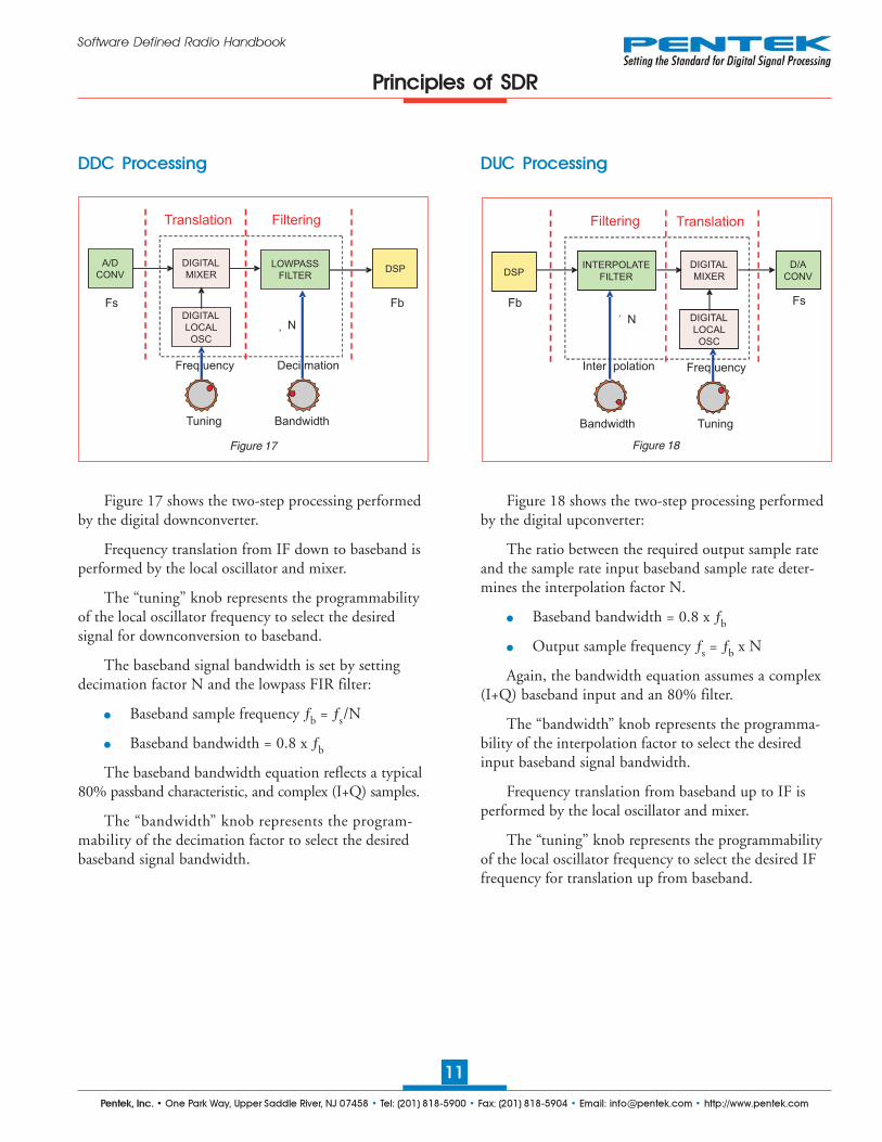
Figure 17 shows the two-step processing performedby the digital downconverter.
Frequency translation from IF down to baseband isperformed by the local oscillator and mixer.
The “tuning” knob represents the programmabilityof the local oscillator frequency to select the desiredsignal for downconversion to baseband.
The baseband signal bandwidth is set by settingdecimation factor N and the lowpass FIR filter:
● Baseband sample frequency ƒb = ƒs/N
● Baseband bandwidth = 0.8 x ƒb
The baseband bandwidth equation reflects a typical80% passband characteristic, and complex (I+Q) samples.
The “bandwidth” knob represents the program-mability of the decimation factor to select the desiredbaseband signal bandwidth.
Figure 18 shows the two-step processing performedby the digital upconverter:
The ratio between the required output sample rateand the sample rate input baseband sample rate deter-mines the interpolation factor N.
● Baseband bandwidth = 0.8 x ƒb
● Output sample frequency ƒs = ƒb x N
Again, the bandwidth equation assumes a complex(I+Q) baseband input and an 80% filter.
The “bandwidth” knob represents the programma-bility of the interpolation factor to select the desiredinput baseband signal bandwidth.
Frequency translation from baseband up to IF isperformed by the local oscillator and mixer.
The “tuning” knob represents the programmabilityof the local oscillator frequency to select the desired IFfrequency for translation up from baseband.
Pentek, Inc. • One Park Way, Upper Saddle River, NJ 07458 • Tel: (201) 818-5900 • Fax: (201) 818-5904 • Email: [email protected] • http://www.pentek.com
12
Software Defined Radio Handbook
Key DDC and DUC Benefits SDR Tasks
Figure 19
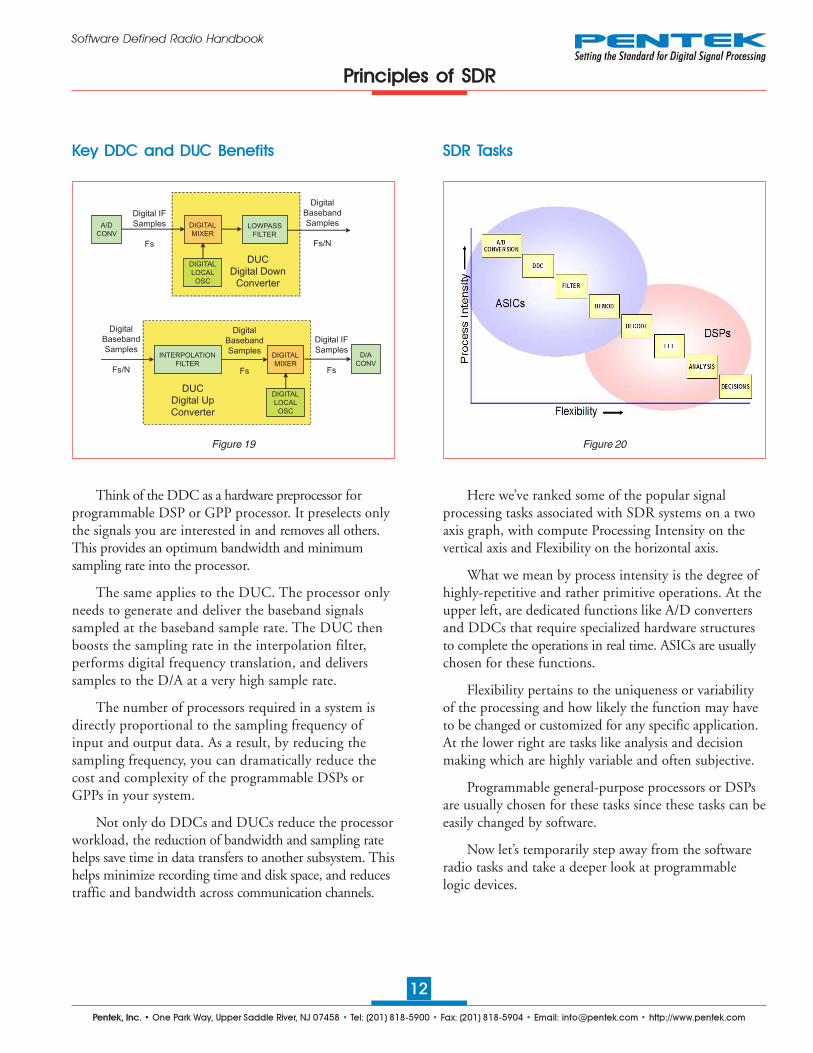
Here we’ve ranked some of the popular signalprocessing tasks associated with SDR systems on a twoaxis graph, with compute Processing Intensity on thevertical axis and Flexibility on the horizontal axis.
What we mean by process intensity is the degree ofhighly-repetitive and rather primitive operations. At theupper left, are dedicated functions like A/D convertersand DDCs that require specialized hardware structuresto complete the operations in real time. ASICs are usuallychosen for these functions.
Flexibility pertains to the uniqueness or variabilityof the processing and how likely the function may haveto be changed or customized for any specific application.At the lower right are tasks like analysis and decisionmaking which are highly variable and often subjective.
Programmable general-purpose processors or DSPsare usually chosen for these tasks since these tasks can beeasily changed by software.
Now let’s temporarily step away from the softwareradio tasks and take a deeper look at programmablelogic devices.
Figure 20
DIGITAL
MIXER
DIGITAL
LOCAL
OSC
A/D
CONV
Digital IF
Samples
Fs
LOWPASS
FILTER
Digital
Baseband
Samples
Fs/N
DUC
Digital Up
Converter
D/A
CONV
Digital
Baseband
Samples
Fs/N
DIGITAL
MIXER
DIGITAL
LOCAL
OSC
INTERPOLATION
FILTER
Digital IF
Samples
Fs
Digital
Baseband
Samples
Fs
DUC
Digital Down
Converter
Think of the DDC as a hardware preprocessor forprogrammable DSP or GPP processor. It preselects onlythe signals you are interested in and removes all others.This provides an optimum bandwidth and minimumsampling rate into the processor.
The same applies to the DUC. The processor onlyneeds to generate and deliver the baseband signalssampled at the baseband sample rate. The DUC thenboosts the sampling rate in the interpolation filter,performs digital frequency translation, and deliverssamples to the D/A at a very high sample rate.
The number of processors required in a system isdirectly proportional to the sampling frequency ofinput and output data. As a result, by reducing thesampling frequency, you can dramatically reduce thecost and complexity of the programmable DSPs orGPPs in your system.
Not only do DDCs and DUCs reduce the processorworkload, the reduction of bandwidth and sampling ratehelps save time in data transfers to another subsystem. Thishelps minimize recording time and disk space, and reducestraffic and bandwidth across communication channels.
Principles of SDR

Pentek, Inc. • One Park Way, Upper Saddle River, NJ 07458 • Tel: (201) 818-5900 • Fax: (201) 818-5904 • Email: [email protected] • http://www.pentek.com
13
Software Defined Radio Handbook
Early Roles for FPGAs Legacy FPGA Design Methodologies
Figure 21 Figure 22
Technology
As true programmable gate functions becameavailable in the 1970’s, they were used extensively byhardware engineers to replace control logic, registers,gates, and state machines which otherwise would haverequired many discrete, dedicated ICs.
Often these programmable logic devices were one-time factory-programmed parts that were soldered downand never changed after the design went into production.
These programmable logic devices were mostly thedomain of hardware engineers and the software toolswere tailored to meet their needs. You had tools foraccepting boolean equations or even schematics to helpgenerate the interconnect pattern for the growingnumber of gates.
Then, programmable logic vendors started offeringpredefined logic blocks for flip-flops, registers andcounters that gave the engineer a leg up on popularhardware functions.
Nevertheless, the hardware engineer was stillintimately involved with testing and evaluating thedesign using the same skills he needed for testingdiscrete logic designs. He had to worry about propaga-tion delays, loading, clocking and synchronizing—alltricky problems that usually had to be solved the hardway—with oscilloscopes or logic analyzers.
� Used primarily to replace discrete digital
hardware circuitry for:
� Control logic
� Glue logic
� Registers and gates
� State machines
� Counters and dividers
� Devices were selected by hardware engineers
� Programmed functions were seldom changed
after the design went into production
� Tools were oriented to hardware engineers
� Schematic processors
� Boolean processors
� Gates, registers, counters, multipliers
� Successful designs required high-level
hardware engineering skills for:
� Critical paths and propagation delays
� Pin assignment and pin locking
� Signal loading and drive capabilities
� Clock distribution
� Input signal synchronization and skew analysis
Pentek, Inc. • One Park Way, Upper Saddle River, NJ 07458 • Tel: (201) 818-5900 • Fax: (201) 818-5904 • Email: [email protected] • http://www.pentek.com
14
Software Defined Radio Handbook
FPGAs: New Device Technology FPGAs: New Development Tools
Figure 23 Figure 24
Technology
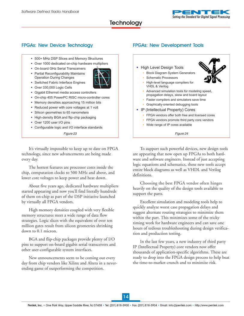
It’s virtually impossible to keep up to date on FPGAtechnology, since new advancements are being madeevery day.
The hottest features are processor cores inside thechip, computation clocks to 500 MHz and above, andlower core voltages to keep power and heat down.
About five years ago, dedicated hardware multipliersstarted appearing and now you’ll find literally hundredsof them on-chip as part of the DSP initiative launchedby virtually all FPGA vendors.
High memory densities coupled with very flexiblememory structures meet a wide range of data flowstrategies. Logic slices with the equivalent of over tenmillion gates result from silicon geometries shrinkingdown to 0.1 micron.
BGA and flip-chip packages provide plenty of I/Opins to support on-board gigabit serial transceivers andother user-configurable system interfaces.
New announcements seem to be coming out everyday from chip vendors like Xilinx and Altera in a never-ending game of outperforming the competition.
To support such powerful devices, new design toolsare appearing that now open up FPGAs to both hard-ware and software engineers. Instead of just acceptinglogic equations and schematics, these new tools acceptentire block diagrams as well as VHDL and Verilogdefinitions.
Choosing the best FPGA vendor often hingesheavily on the quality of the design tools available tosupport the parts.
Excellent simulation and modeling tools help toquickly analyze worst case propagation delays andsuggest alternate routing strategies to minimize themwithin the part. This minimizes some of the trickytiming work for hardware engineers and can save onehours of tedious troubleshooting during design verifica-tion and production testing.
In the last few years, a new industry of third partyIP (Intellectual Property) core vendors now offerthousands of application-specific algorithms. These areready to drop into the FPGA design process to help beatthe time-to-market crunch and to minimize risk.
� 500+ MHz DSP Slices and Memory Structures
� Over 1000 dedicated on-chip hardware multipliers
� On-board GHz Serial Transceivers
� Partial Reconfigurability Maintains
Operation During Changes
� Switched Fabric Interface Engines
� Over 330,000 Logic Cells
� Gigabit Ethernet media access controllers
� On-chip 405 PowerPC RISC micro-controller cores
� Memory densities approaching 15 million bits
� Reduced power with core voltages at 1 volt
� Silicon geometries to 65 nanometers
� High-density BGA and flip-chip packaging
� Over 1200 user I/O pins
� Configurable logic and I/O interface standards
� High Level Design Tools
� Block Diagram System Generators
� Schematic Processors
� High-level language compilers for
VHDL & Verilog
� Advanced simulation tools for modeling speed,
propagation delays, skew and board layout
� Faster compilers and simulators save time
� Graphically-oriented debugging tools
� IP (Intellectual Property) Cores
� FPGA vendors offer both free and licensed cores
� FPGA vendors promote third party core vendors
� Wide range of IP cores available
Pentek, Inc. • One Park Way, Upper Saddle River, NJ 07458 • Tel: (201) 818-5900 • Fax: (201) 818-5904 • Email: [email protected] • http://www.pentek.com
15
Software Defined Radio Handbook
FPGAs for SDR FPGAs Bridge the SDR Application Space
Figure 25 Figure 26
Technology
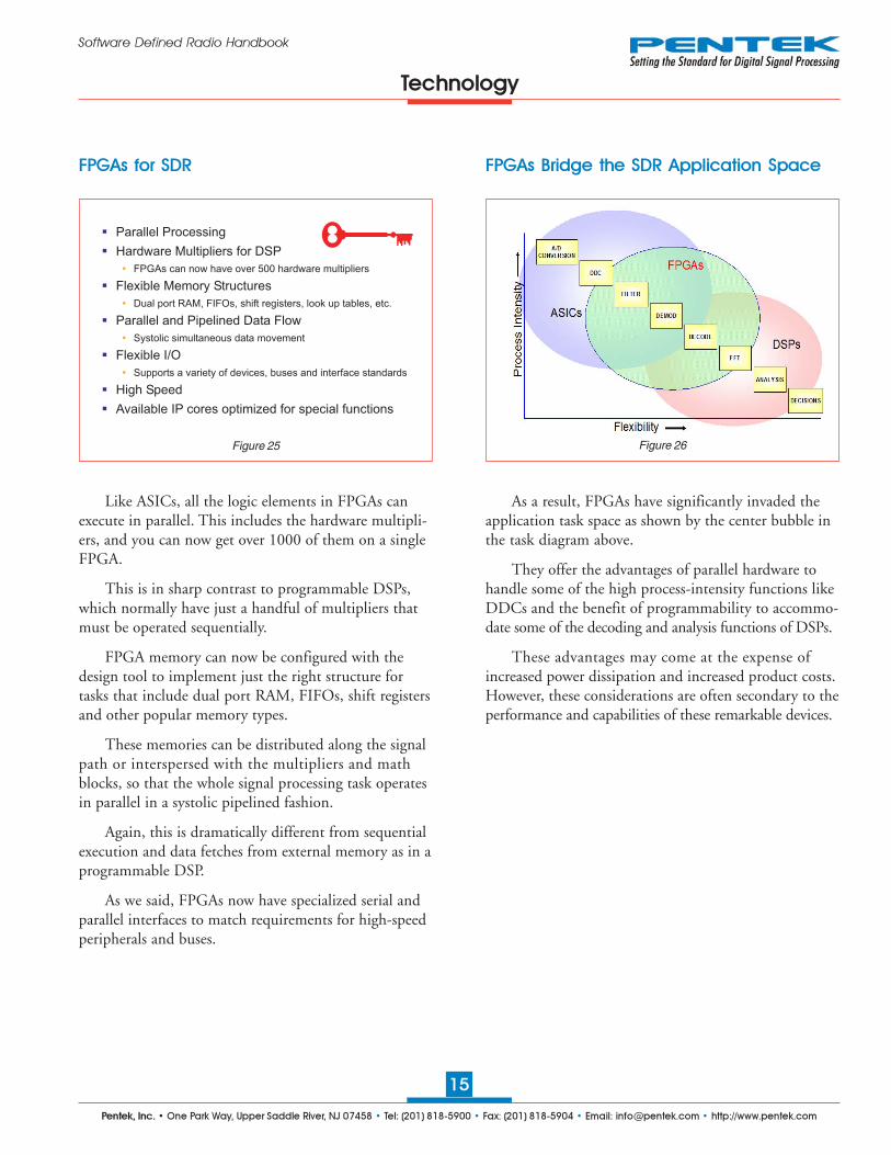
As a result, FPGAs have significantly invaded theapplication task space as shown by the center bubble inthe task diagram above.
They offer the advantages of parallel hardware tohandle some of the high process-intensity functions likeDDCs and the benefit of programmability to accommo-date some of the decoding and analysis functions of DSPs.
These advantages may come at the expense ofincreased power dissipation and increased product costs.However, these considerations are often secondary to theperformance and capabilities of these remarkable devices.
Like ASICs, all the logic elements in FPGAs canexecute in parallel. This includes the hardware multipli-ers, and you can now get over 1000 of them on a singleFPGA.
This is in sharp contrast to programmable DSPs,which normally have just a handful of multipliers thatmust be operated sequentially.
FPGA memory can now be configured with thedesign tool to implement just the right structure fortasks that include dual port RAM, FIFOs, shift registersand other popular memory types.
These memories can be distributed along the signalpath or interspersed with the multipliers and mathblocks, so that the whole signal processing task operatesin parallel in a systolic pipelined fashion.
Again, this is dramatically different from sequentialexecution and data fetches from external memory as in aprogrammable DSP.
As we said, FPGAs now have specialized serial andparallel interfaces to match requirements for high-speedperipherals and buses.
� Parallel Processing
� Hardware Multipliers for DSP
� FPGAs can now have over 500 hardware multipliers
� Flexible Memory Structures
� Dual port RAM, FIFOs, shift registers, look up tables, etc.
� Parallel and Pipelined Data Flow
� Systolic simultaneous data movement
� Flexible I/O
� Supports a variety of devices, buses and interface standards
� High Speed
� Available IP cores optimized for special functions
Pentek, Inc. • One Park Way, Upper Saddle River, NJ 07458 • Tel: (201) 818-5900 • Fax: (201) 818-5904 • Email: [email protected] • http://www.pentek.com
16
Software Defined Radio Handbook
ModelModel
FeatureFeature7141-4307141-430 7141-4207141-420 7142-4287142-428 71517151 71527152 71537153
125 MHz125 MHzMax Sample RateMax Sample Rate 125 MHz125 MHz 125 MHz125 MHz 200 MHz200 MHz 200 MHz200 MHz 200 MHz200 MHz
14-Bit14-BitInput ResolutionInput Resolution 14-Bit14-Bit 14-Bit14-Bit 16-Bit16-Bit 16-Bit16-Bit 16-Bit16-Bit
11Input ChannelsInput Channels 22 44 44 44 44
256256DDC ChannelsDDC Channels 2 or 42 or 4 44 256256 3232 2 or 42 or 4
1K-10K1K-10KDecimation RangeDecimation Range Core: 2,4,8,16,32,64
GC4016: 32to 16k
Core: 2,4,8,16,32,64
GC4016: 32to 16k2 to 64K
Steps of 1
2 to 64K
Steps of 1128 to 1024
Steps of 64
128 to 1024
Steps of 6416 to 8192
Steps of 8
16 to 8192
Steps of 82 Ch: 2 to 65536
4 Ch: 2 to 256
2 Ch: 2 to 65536
4 Ch: 2 to 256
24*DEC/51224*DEC/512No. of Filter TapsNo. of Filter Taps Core: 28*DECCore: 28*DEC 28*DEC28*DEC 24*DEC/6424*DEC/64 28*DEC/828*DEC/8 28*DEC28*DEC
Normal I/QNormal I/QOutput FormatOutput Format I/Q, Offset,
Inverse, Real
I/Q, Offset,
Inverse, RealI/Q,
Offset, Inverse
I/Q,
Offset, InverseI/Q,
Offset, Inverse
I/Q,
Offset, InverseI/Q,
Offset, Inverse
I/Q,
Offset, InverseI/Q,
Offset, Inverse
I/Q,
Offset, Inverse
16-Bit16-BitOutput ResolutionOutput Resolution 16-Bit, 24-Bit16-Bit, 24-Bit 16-Bit, 24-Bit16-Bit, 24-Bit 16-Bit, 24-Bit16-Bit, 24-Bit 16-Bit, 24-Bit16-Bit, 24-Bit 16-Bit, 24-Bit16-Bit, 24-Bit
32-bits - 0 to Fs32-bits - 0 to FsTuning FrequencyTuning Frequency 32-bits - 0 to Fs32-bits - 0 to Fs 32-bits - 0 to Fs32-bits - 0 to Fs 32-bits - 0 to Fs32-bits - 0 to Fs 32-bits - 0 to Fs32-bits - 0 to Fs 32-bits - 0 to Fs32-bits - 0 to Fs
--Phase OffsetPhase Offset 32-bits ± 180 deg32-bits ± 180 deg 32-bits ± 180 deg32-bits ± 180 deg 32-bits ± 180 deg32-bits ± 180 deg 32-bits ± 180 deg32-bits ± 180 deg 32-bits ± 180 deg32-bits ± 180 deg
32 bits32 bitsGain ControlGain Control 32 bits32 bits 32 bits32 bits 32 bits32 bits 32 bits32 bits 32 bits32 bits
NoneNoneDAC InterpolationDAC Interpolation 2 - 327682 - 32768 2 - 327682 - 32768 NoneNone NoneNone NoneNone
NoneNonePower MetersPower Meters NoneNone NoneNone NoneNone 3232 2 or 42 or 4
NoneNoneThresh DetectorsThresh Detectors NoneNone NoneNone NoneNone 3232 2 or 42 or 4
NoneNoneChannel SummersChannel Summers NoneNone NoneNone NoneNone 32 channels32 channels 2 or 4 channels2 or 4 channels
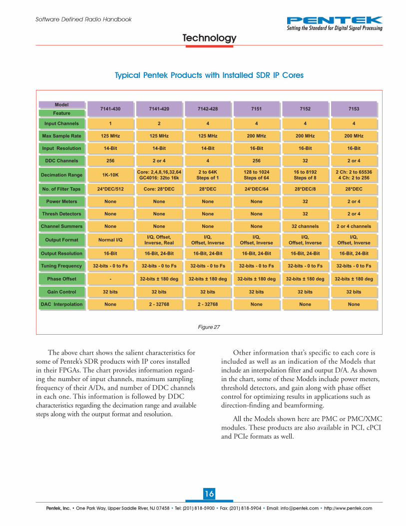
The above chart shows the salient characteristics forsome of Pentek’s SDR products with IP cores installedin their FPGAs. The chart provides information regard-ing the number of input channels, maximum samplingfrequency of their A/Ds, and number of DDC channelsin each one. This information is followed by DDCcharacteristics regarding the decimation range and availablesteps along with the output format and resolution.
Technology
Typical Pentek Products with Installed SDR IP Cores
Other information that’s specific to each core isincluded as well as an indication of the Models thatinclude an interpolation filter and output D/A. As shownin the chart, some of these Models include power meters,threshold detectors, and gain along with phase offsetcontrol for optimizing results in applications such asdirection-finding and beamforming.
All the Models shown here are PMC or PMC/XMCmodules. These products are also available in PCI, cPCIand PCIe formats as well.
Figure 27

Pentek, Inc. • One Park Way, Upper Saddle River, NJ 07458 • Tel: (201) 818-5900 • Fax: (201) 818-5904 • Email: [email protected] • http://www.pentek.com
17
Software Defined Radio Handbook
Technology
FPGA Resource Comparison
Figure 28
The above chart compares the available resources inthe four Xilinx FPGA families that are used in most ofthe Pentek products.
● Virtex-II Pro: VP50 and VP70● Virtex-4: FX, LX and SX● Virtex-5: FXT, LXT and SXT● Virtex-6: LXT and SXT
The Virtex-II family includes hardware multipliersthat support digital filters, averagers, demodulatorsand FFTs—a major benefit for software radio signalprocessing. The Virtex-II Pro family dramaticallyincreased the number of hardware multipliers and alsoadded embedded PowerPC microcontrollers.
The Virtex-4 family is offered as three subfamiliesthat dramatically boost clock speeds and reduce powerdissipation over previous generations.
The Virtex-4 LX family delivers maximum logicand I/O pins while the SX family boasts of 512 DSPslices for maximum DSP performance. The FX family isa generous mix of all resources and is the only family tooffer RocketIO, PowerPC cores, and the newly addedgigabit Ethenet ports.
*Virtex-II Pro and Virtex-4 Slices actually require 2.25 Logic Cells;
Virtex-5 and Virtex-6 Slices actually require 6.4 Logic Cells
Virtex-II Pro Virtex-4 Virtex-5 Virtex-6
VP50, VP70 FX, LX, SX FXT, LXT, SXT LXT, SXT
Logic Cells 53K–74K 41K–152K 46K–156K 128K–476K
Slices* 24K–33K 18K–68K 7K–24K 20K–74K
CLB Flip-Flops 47K–66K 49K–93K 150K–207K 160K–595K
Block RAM (kb) 4,176–5,904 1,728–6,768 2,160–8,784 9,504–38,304
DSP Hard IP 18x18 Multipliers DSP48 DSP48E DSP48E
DSP Slices 132–328 64–512 48–640 480–2,016
Serial Gbit Transceivers – 0–20 12–16 20
PCI Express Blocks – – – 2
SelectIO – 448–768 480–640 600
The Virtex-5 family LXT devices offer maximumlogic resources, gigabit serial transceivers, and Ethernetmedia access controllers. The SXT devices push DSPcapabilities with all of the same extras as the LXT. TheFXT devices follow as the embedded system resource devices.
The Virtex-5 devices offer lower power dissipation,faster clock speeds and enhanced logic slices. They alsoimprove the clocking features to handle faster memoryand gigabit interfaces. They support faster single-endedand differential parallel I/O buses to handle fasterperipheral devices.
The Virtex-6 devices offer higher density, moreprocessing power, lower power consumption, andupdated interface features to match the latest technologyI/O requirements including PCI Express. Virtex-6supports PCI Express 2.0 in x1 through x8 configurations.
The ample DSP slices are responsible for themajority of the processing power of the Virtex-6 family.Increases in operating speed from 500 MHz in V-4 to550 MHz in V-5 to 600 MHz in V-6 and increasingdensity allows more DSP slices to be included in thesame-size package. As shown in the chart, Virtex-6 topsout at an impressive 2016 DSP slices.
Pentek, Inc. • One Park Way, Upper Saddle River, NJ 07458 • Tel: (201) 818-5900 • Fax: (201) 818-5904 • Email: [email protected] • http://www.pentek.com
18
Software Defined Radio Handbook
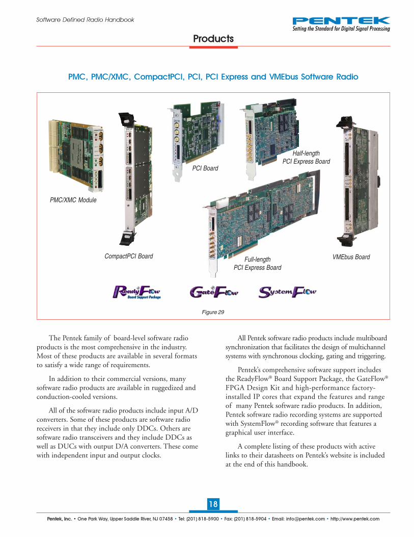
PMC, PMC/XMC, CompactPCI, PCI, PCI Express and VMEbus Software Radio
The Pentek family of board-level software radioproducts is the most comprehensive in the industry.Most of these products are available in several formatsto satisfy a wide range of requirements.
In addition to their commercial versions, manysoftware radio products are available in ruggedized andconduction-cooled versions.
All of the software radio products include input A/Dconverters. Some of these products are software radioreceivers in that they include only DDCs. Others aresoftware radio transceivers and they include DDCs aswell as DUCs with output D/A converters. These comewith independent input and output clocks.
All Pentek software radio products include multiboardsynchronization that facilitates the design of multichannelsystems with synchronous clocking, gating and triggering.
Pentek’s comprehensive software support includesthe ReadyFlow® Board Support Package, the GateFlow®
FPGA Design Kit and high-performance factory-installed IP cores that expand the features and rangeof many Pentek software radio products. In addition,Pentek software radio recording systems are supportedwith SystemFlow® recording software that features agraphical user interface.
A complete listing of these products with activelinks to their datasheets on Pentek’s website is includedat the end of this handbook.
PMC/XMC Module
Products
Figure 29
CompactPCI Board
PCI Board
VMEbus BoardFull-lengthPCI Express Board
Half-lengthPCI Express Board

Pentek, Inc. • One Park Way, Upper Saddle River, NJ 07458 • Tel: (201) 818-5900 • Fax: (201) 818-5904 • Email: [email protected] • http://www.pentek.com
19
Software Defined Radio Handbook
Multiband Receivers
The unit supports the channel combining mode ofthe 4016s such that two or four individual 2.5 MHzchannels can be combined for output bandwidths of5 MHz or 10 MHz, respectively.
The sampling clock can be sourced from an internal100 MHz crystal oscillator or from an external clock suppliedthrough an SMA connector or the LVDS clock/sync bus onthe front panel. The LVDS bus allows multiple modules to besynchronized with the same sample clock, gating, triggeringand frequency switching signals. Up to 80 modules can besynchronized with the Model 9190 Clock and Sync Genera-tor. Custom interfaces can be implemented by using the 64user-defined FPGA I/O pins on the P4 connector.
Versions of the 7131 are also available as a PCIboard (Model 7631A), 6U cPCI (Models 7231 and7231D dual density), or 3U cPCI (Model 7331). Allthese products have similar features.
Products
The Model 7131, a 16-Channel Multiband Receiver,is a PMC module. The 7131 PMC may be attached to awide range of industry processor platforms equippedwith PMC sites.
Two 14-bit 105 MHz A/D Converters accepttransformer-coupled RF inputs through two front panelSMA connectors. Both inputs are connected to fourTI/GC4016 quad DDC chips, so that all 16 DDCchannels can independently select either A/D.
Four parallel outputs from the four DDCs deliverdata into the Virtex-II FPGA which can be either theXC2V1000 or XC2V3000. The outputs of the two A/Dconverters are also connected directly to the FPGA tosupport the DDC bypass path to the PCI bus and for directprocessing of the wideband A/D signals by the FPGA.
Model 7131 PMC ●●●●● Model 7231 6U cPCI ●●●●● Model 7331 3U cPCI ●●●●● Model 7631A PCI
Figure 30
Model 7231D6U cPCI
Model 73313U cPCI
Model 7631APCI
Model 7131PMC
Pentek, Inc. • One Park Way, Upper Saddle River, NJ 07458 • Tel: (201) 818-5900 • Fax: (201) 818-5904 • Email: [email protected] • http://www.pentek.com
20
Software Defined Radio Handbook
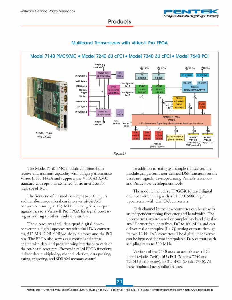
Multiband Transceivers with Virtex-II Pro FPGA
Products
Figure 31
Model 7140 PMC/XMC ●●●●● Model 7240 6U cPCI ●●●●● Model 7340 3U cPCI ●●●●● Model 7640 PCI
Model 7140PMC/XMC
The Model 7140 PMC module combines bothreceive and transmit capability with a high-performanceVirtex II-Pro FPGA and supports the VITA 42 XMCstandard with optional switched fabric interfaces forhigh-speed I/O.
The front end of the module accepts two RF inputsand transformer-couples them into two 14-bit A/Dconverters running at 105 MHz. The digitized outputsignals pass to a Virtex-II Pro FPGA for signal process-ing or routing to other module resources.
These resources include a quad digital down-converter, a digital upconverter with dual D/A convert-ers, 512 MB DDR SDRAM delay memory and the PCIbus. The FPGA also serves as a control and statusengine with data and programming interfaces to each ofthe on-board resources. Factory-installed FPGA functionsinclude data multiplexing, channel selection, data packing,gating, triggering, and SDRAM memory control.
In addition to acting as a simple transceiver, themodule can perform user-defined DSP functions on thebaseband signals, developed using Pentek’s GateFlowand ReadyFlow development tools.
The module includes a TI/GC4016 quad digitaldownconverter along with a TI DAC5686 digitalupconverter with dual D/A converters.
Each channel in the downconverter can be set withan independent tuning frequency and bandwidth. Theupconverter translates a real or complex baseband signal toany IF center frequency from DC to 160 MHz and candeliver real or complex (I + Q) analog outputs throughits two 16-bit D/A converters. The digital upconvertercan be bypassed for two interpolated D/A outputs withsampling rates to 500 MHz.
Versions of the 7140 are also available as a PCIboard (Model 7640), 6U cPCI (Models 7240 and7240D dual density), or 3U cPCI (Model 7340). Allthese products have similar features.
VIRTEX-II Pro FPGA
XC2VP50
DSP – Channelizer – Digital Delay – Demodulation – Decoding – Control – etc.Control/
Status
GC4016
4-CHANNEL
DIGITAL
RECEIVER
16
16
16
14
24
FLASH
16 MB
16
DDR
SDRAM
256 MB
DDR
SDRAM
128 MB
DDR
SDRAM
128 MB
32 32 32
PCI 2.2 INTERFACE
(64 Bits / 66 MHz)
PCI BUS
(64 Bits / 66 MHz)
64
TIMING BUS
GENERATOR A
XTL
OSC A
SYNC
INTERRUPTS
& CONTROL
TIMING BUS
GENERATOR B
XTL
OSC B
Sample
Clock B In
Sample
Clock A In
LVDS Clock A
LVDS Sync A
LVDS Gate A
TTL Gate/
Trigger
TTL Sync
LVDS Clock B
LVDS Sync B
LVDS Gate B
Clock/Sync/Gate
Bus A
Clock/Sync/Gate
Bus B
To All
Sections
32
RF XFORMR RF XFORMR
RF Out RF Out
DAC5686
DIGITAL UPCONVERTER
16-bit D/A 16-bit D/A
14
RF
XFORMR
RF
XFORMR
RF In RF In
14
AD6645
105 MHz
14-bit A/D
AD6645
105 MHz
14-bit A/D
P15 XMC
VITA 42.0
(Serial RapidIO,
PCI-Express, etc.)
P4 PMC
FPGA I/O
(Option –104)
648X

Pentek, Inc. • One Park Way, Upper Saddle River, NJ 07458 • Tel: (201) 818-5900 • Fax: (201) 818-5904 • Email: [email protected] • http://www.pentek.com
21
Software Defined Radio Handbook
Products
Transceivers with Dual Wideband DDC and Interpolation Filter Installed Cores
Model 7140-420 PMC/XMC ●●●●● Model 7240-420 6U cPCI
Model 7340-420 3U cPCI ●●●●● Model 7640-420 PCI
Figure 32
The Pentek IP Core 420 includes a dual high-performance wideband DDC and an interpolation filter.Factory-installed in the Model 7140 FPGA, they extendthe range of both the GC4016 ASIC DDC and theDAC5686 DUC.
Like the GC4016, each of the core 420 DDCstranslates any frequency band within the input band-width range down to zero frequency. A complex FIR lowpass filter removes any out-of-band frequency components.An output decimator and formatter deliver either complexor real data. An input gain block scales both I and Qdata streams by a 16-bit gain term.
The mixer utilizes four 18x18-bit multipliers tohandle the complex inputs from the NCO and thecomplex data input samples. The FIR filter is capable ofstoring and utilizing up to four independent sets of18-bit coefficients for each decimation value. Thesecoefficients are user-programmable by using RAMstructures within the FPGA.
The decimation settings of 2, 4, 8, 16, 32, and 64provide output bandwidths from 40 MHz down to1.25 MHz for an A/D sampling of 100 MHz. A multi-plexer in front of the Core 420 DDCs allows data to besourced from either the A/Ds or the GC4016, extendingthe maximum cascaded decimation range to 1,048,576.
The interpolation filter included in the 420 Core,expands the interpolation factor from 2 to 32,768programmable in steps of 2, and relieves the hostprocessor from performing upsampling tasks. Includingthe DUC, the maximum interpolation factor is 32,768which is comparable to the maximum decimation of theGC4016 narrowband DDC.
In addition to the Core 420, all the standardfeatures of the 7140 are retained.
Versions of the 7140-420 are also available as a PCIboard (Model 7640-420), 6U cPCI (Models 7240-420and 7240D-420 dual density), or 3U cPCI (Model7340-420). All these products have similar features.
.
RF
XFORMR
RF
XFORMR
RF
XFORMR
RF
XFORMR
AD6645
105 MHz
14-bit A/D
AD6645
105 MHz
14-bit A/D
CLOCK &
SYNC
GENERATOR
XTAL
OSC A
XTAL
OSC B
MUX
GC4016 DIGITAL
DOWNCONVERTR
DAC 5686
DIGITAL
UPCONVERTER
16-bit
500 MHZ
D/A
16-bit
500 MHZ
D/A
128 MB DDR
SDRAM
128 MB DDR
SDRAM
256 MB DDR
SDRAM
PCI 2.2
INTERFACE
MEMORY
CONTROL
&
DATA ROUTING
MEM W
FIFO
MEM W
FIFO
A/D A
FIFO
A/D B
FIFO
DDC A
FIFO
DDC B
FIFO
DDC C
FIFO
DDC D
FIFO
D/A A
FIFO
D/A B
FIFO
MUX
MUX
CFIR
FILTER
CIC
FILTER
MUX
WIDEBAND
DIGITAL
DOWNCONVERTR A
DECIMATION: 2 – 64
WIDEBAND
DIGITAL
DOWNCONVERTR A
DECIMATION: 2 – 64
M
U
X
M
U
X
MUX
CH A
RF In
CH B
RF In
CH A
RF Out
CH B
RF Out
Sample
Clock A In
Clock/Sync
Bus
Sample
Clock B In
A B C D
A B C D
MEMORY
MEMORY
DDC C
DDC D
D/A A
D/A B
A/D A
A/D B
A/D A
A/D B
DDC A
DDC B
A/D A
A/D B
DDC A
DDC BWB DDC A
DDC A
WB DDC B
DDC B
MEMORY
D/A A FIFO
MEMORY
D/A B FIFO
PCI BUS
64 bit /
66 MHz
WIDEBAND DDC CORE
INTERPOLATION CORE
XC2VP50
RF
XFORMR
RF
XFORMR
RF
XFORMR
RF
XFORMR
AD6645
105 MHz
14-bit A/D
AD6645
105 MHz
14-bit A/D
CLOCK &
SYNC
GENERATOR
XTAL
OSC A
XTAL
OSC B
MUX
GC4016 DIGITAL
DOWNCONVERTR
DAC 5686
DIGITAL
UPCONVERTER
16-bit
500 MHZ
D/A
16-bit
500 MHZ
D/A
128 MB DDR
SDRAM
128 MB DDR
SDRAM
256 MB DDR
SDRAM
PCI 2.2
INTERFACE
Pentek, Inc. • One Park Way, Upper Saddle River, NJ 07458 • Tel: (201) 818-5900 • Fax: (201) 818-5904 • Email: [email protected] • http://www.pentek.com
22
Software Defined Radio Handbook
Model 7140-430 PMC/XMC ●●●●● Model 7240-430 6U cPCI
Model 7340-430 3U cPCI ●●●●● Model 7640-430 PCI
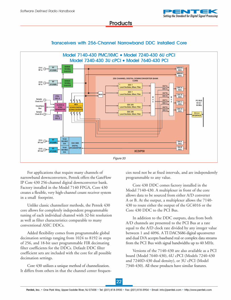
Transceivers with 256-Channel Narrowband DDC Installed Core
Products
Figure 33
For applications that require many channels ofnarrowband downconverters, Pentek offers the GateFlowIP Core 430 256-channel digital downconverter bank.Factory installed in the Model 7140 FPGA, Core 430creates a flexible, very high-channel count receiver systemin a small footprint.
Unlike classic channelizer methods, the Pentek 430core allows for completely independent programmabletuning of each individual channel with 32-bit resolutionas well as filter characteristics comparable to manyconventional ASIC DDCs.
Added flexibility comes from programmable globaldecimation settings ranging from 1024 to 8192 in stepsof 256, and 18-bit user programmable FIR decimatingfilter coefficients for the DDCs. Default DDC filtercoefficient sets are included with the core for all possibledecimation settings.
Core 430 utilizes a unique method of channelization.It differs from others in that the channel center frequen-
cies need not be at fixed intervals, and are independentlyprogrammable to any value.
Core 430 DDC comes factory installed in theModel 7140-430. A multiplexer in front of the coreallows data to be sourced from either A/D converterA or B. At the output, a multiplexer allows the 7140-430 to route either the output of the GC4016 or theCore 430 DDC to the PCI Bus.
In addition to the DDC outputs, data from bothA/D channels are presented to the PCI Bus at a rateequal to the A/D clock rate divided by any integer valuebetween 1 and 4096. A TI DAC5686 digital upconverterand dual D/A accepts baseband real or complex data streamsfrom the PCI Bus with signal bandwidths up to 40 MHz.
Versions of the 7140-430 are also available as a PCIboard (Model 7640-430), 6U cPCI (Models 7240-430and 7240D-430 dual density), or 3U cPCI (Model7340-430). All these products have similar features.
.
RF
XFORMR
RF
XFORMR
RF
XFORMR
RF
XFORMR
AD6645
105 MHz
14-bit A/D
AD6645
105 MHz
14-bit A/D
CLOCK &
SYNC
GENERATOR
XTAL
OSC A
XTAL
OSC B
MUX
GC4016 DIGITAL
DOWNCONVERTR
DAC 5686
DIGITAL
UPCONVERTER
16-bit
500 MHZ
D/A
16-bit
500 MHZ
D/A
PCI 2.2
INT
MEM W
FIFO
MEM W
FIFO
D/A A
FIFO
D/A B
FIFO
CH A
RF In
CH B
RF In
CH A
RF Out
CH B
RF Out
Sample
Clock A In
Clock/Sync
Bus
Sample
Clock B In
A B C D
A B C D
DDC 1
Local Oscillator, Mixer, Filter
M
U
X
1
2
255
256
MUX
M
U
X
DDC A
FIFO
DDC B
FIFO
DDC C
FIFO
DDC D
FIFO
OUT A
DDC A
OUT B
DDC B
OUT C
DDC C
OUT D
DDC D
PCI BUS
64 bit /
66 MHz
256 CHANNEL DIGITAL DOWNCONVERTER BANK
CORE
XC2VP50
RF
XFORMR
RF
XFORMR
RF
XFORMR
RF
XFORMR
AD6645
105 MHz
14-bit A/D
AD6645
105 MHz
14-bit A/D
CLOCK &
SYNC
GENERATOR
XTAL
OSC A
XTAL
OSC B
MUX
GC4016 DIGITAL
DOWNCONVERTR
DAC 5686
DIGITAL
UPCONVERTER
16-bit
500 MHZ
D/A
16-bit
500 MHZ
D/A
PCI 2.2
INTERFACE
DDC 1
Local Oscillator, Mixer, Filter
DDC 255
Local Oscillator, Mixer, Filter
DDC 256
Local Oscillator, Mixer, Filter

Pentek, Inc. • One Park Way, Upper Saddle River, NJ 07458 • Tel: (201) 818-5900 • Fax: (201) 818-5904 • Email: [email protected] • http://www.pentek.com
23
Software Defined Radio Handbook
Multiband Transceivers with Virtex-II Pro FPGA
Products
Figure 34
Model 7141PMC/XMC
AD6645
105 MHz
14-BIT A/D
AD6645
105 MHz
14-BIT A/D
TIMING BUS
GENERATOR A
XTL
OSC A
SYNC
INTERRUPTS
& CONTROL
TIMING BUS
GENERATOR B
XTL
OSC B
RF
XFORMR
RF
XFORMR
GC4016
4-CHANNEL
DIGITAL
RECEIVER
VIRTEX-II Pro FPGA
XC2VP50
DSP – Channelizer – Digital Delay – Demodulation – Decoding – Control – etc.
FLASH
16 MB
DDR
SDRAM
256 MB
DDR
SDRAM
128 MB
DDR
SDRAM
128 MBPCI 2.2 INTERFACE
(64 Bits / 66 MHz)
Sample
Clock B In
Sample
Clock A In
LVDS Clock A
LVDS Sync A
LVDS Gate A
TTL Gate/
Trigger
TTL Sync
LVDS Clock B
LVDS Sync B
LVDS Gate B
RF In RF In
Clock/Sync/Gate
Bus A
Clock/Sync/Gate
Bus B
To All
Sections Control/
Status
PCI BUS
(64 Bits / 66 MHz)
P15 XMC
VITA 42.0
(Serial RapidIO,
PCI-Express, etc.)
P4 PMC
FPGA I/O
(Option –104)
14 14
16
16
16
14
24
32
16
32 32 3264 64
RF XFORMR RF XFORMR
RF Out RF Out
DAC5686
DIGITAL UPCONVERTER
16-bit D/A 16-bit D/A
LTC2255
125 MHz
14-bit A/D
LTC2255
125 MHz
14-bit A/D
FRONT
PANEL
CONNECTOR
The Model 7141 PMC/XMC module combinesboth receive and transmit capabilities with a high-performance Virtex II-Pro FPGA and supports theVITA 42 XMC standard with optional switched fabricinterfaces for high-speed I/O.
The front end of the module accepts two RF inputsand transformer-couples them into two 14-bit A/Dconverters running at 125 MHz. The digitized outputsignals pass to a Virtex-II Pro FPGA for signal process-ing or routing to other module resources.
These resources include a quad digital down-converter, a digital upconverter with dual D/A converters,512 MB DDR SDRAM delay memory and the PCIbus. The FPGA also serves as a control and statusengine with data and programming interfaces to each ofthe on-board resources. Factory-installed FPGA functionsinclude data multiplexing, channel selection, data packing,gating, triggering, and SDRAM memory control.
In addition to acting as a simple transceiver, themodule can perform user-defined DSP functions on the
baseband signals, developed using Pentek’s GateFlowand ReadyFlow development tools.
The module includes a TI/GC4016 quad digitaldownconverter along with a TI DAC5686 digitalupconverter with dual D/A converters.
Each channel in the downconverter can be set withan independent tuning frequency and bandwidth. Theupconverter translates a real or complex baseband signal toany IF center frequency from DC to 160 MHz and candeliver real or complex (I + Q) analog outputs throughits two 16-bit D/A converters. The digital upconvertercan be bypassed for two interpolated D/A outputs withsampling rates to 500 MHz.
Versions of the 7141 are also available as a PCIefull-length board (Models 7741 and 7741D dual density),PCIe half-length board (Model 7841), PCI board(Model 7641), 6U cPCI (Models 7241 and 7241Ddual density), and 3U cPCI (Model 7341).
Model 7141-703 is a conduction-cooled version.
Model 7141 PMC/XMC ●●●●● Model 7241 6U cPCI ●●●●● Model 7341 3U cPCI
Model 7641 PCI ●●●●● Model 7741 Full-length PCIe ●●●●● Model 7841 Half-length PCIe

Pentek, Inc. • One Park Way, Upper Saddle River, NJ 07458 • Tel: (201) 818-5900 • Fax: (201) 818-5904 • Email: [email protected] • http://www.pentek.com
24
Software Defined Radio Handbook
Products
Transceivers with Dual Wideband DDC and Interpolation Filter Installed Cores
Figure 35
.
RF
XFORMR
RF
XFORMR
RF
XFORMR
RF
XFORMR
AD6645
105 MHz
14-bit A/D
AD6645
105 MHz
14-bit A/D
CLOCK &
SYNC
GENERATOR
XTAL
OSC A
XTAL
OSC B
MUX
GC4016 DIGITAL
DOWNCONVERTR
DAC 5686
DIGITAL
UPCONVERTER
16-bit
500 MHZ
D/A
16-bit
500 MHZ
D/A
128 MB DDR
SDRAM
128 MB DDR
SDRAM
256 MB DDR
SDRAM
PCI 2.2
INTERFACE
MEMORY
CONTROL
&
DATA ROUTING
MEM W
FIFO
MEM W
FIFO
A/D A
FIFO
A/D B
FIFO
DDC A
FIFO
DDC B
FIFO
DDC C
FIFO
DDC D
FIFO
D/A A
FIFO
D/A B
FIFO
MUX
MUX
CFIR
FILTER
CIC
FILTER
MUX
WIDEBAND
DIGITAL
DOWNCONVERTR A
DECIMATION: 2 – 64
WIDEBAND
DIGITAL
DOWNCONVERTR A
DECIMATION: 2 – 64
M
U
X
M
U
X
MUX
CH A
RF In
CH B
RF In
CH A
RF Out
CH B
RF Out
Sample
Clock A In
Clock/Sync
Bus
Sample
Clock B In
A B C D
A B C D
MEMORY
MEMORY
DDC C
DDC D
D/A A
D/A B
A/D A
A/D B
A/D A
A/D B
DDC A
DDC B
A/D A
A/D B
DDC A
DDC BWB DDC A
DDC A
WB DDC B
DDC B
MEMORY
D/A A FIFO
MEMORY
D/A B FIFO
PCI BUS
64 bit /
66 MHz
WIDEBAND DDC CORE
INTERPOLATION CORE
XC2VP50
RF
XFORMR
RF
XFORMR
RF
XFORMR
RF
XFORMR
LTC2255
125 MHz
14-bit A/D
LTC2255
125 MHz
14-bit A/D
CLOCK &
SYNC
GENERATOR
XTAL
OSC A
XTAL
OSC B
MUX
GC4016 DIGITAL
DOWNCONVERTR
DAC 5686
DIGITAL
UPCONVERTER
16-bit
500 MHZ
D/A
16-bit
500 MHZ
D/A
128 MB DDR
SDRAM
128 MB DDR
SDRAM
256 MB DDR
SDRAM
PCI 2.2
INTERFACE
Model 7141-420 PMC/XMC ●●●●● Model 7241-420 6U cPCI ●●●●● Model 7341-420 3U cPCI
Model 7641-420 PCI ●●●●● Model 7741-420 Full-length PCIe ●●●●● Model 7841-420 Half-length PCIe
The Pentek IP Core 420 includes a dual high-performance wideband DDC and an interpolation filter.Factory-installed in the Model 7141 FPGA, they extendthe range of both the GC4016 ASIC DDC and theDAC5686 DUC.
Each of the core 420 DDCs translates any frequencyband within the input bandwidth range down to zerofrequency. A complex FIR low pass filter removes any out-of-band frequency components. An output decimator andformatter deliver either complex or real data. An input gainblock scales both I and Q data streams by a 16-bit gainterm.
The mixer utilizes four 18x18-bit multipliers tohandle the complex inputs from the NCO and thecomplex data input samples. The FIR filter is capable ofstoring and utilizing up to four independent sets of18-bit coefficients for each decimation value. Thesecoefficients are user-programmable by using RAMstructures within the FPGA.
The decimation settings of 2, 4, 8, 16, 32, and 64provide output bandwidths from 40 MHz down to 1.25MHz for an A/D sampling of 100 MHz. A multiplexerin front of the Core 420 DDCs allows data to be sourcedfrom either the A/Ds or the GC4016, extending themaximum cascaded decimation range to 1,048,576.
The interpolation filter included in the 420 Core,expands the interpolation factor from 2 to 32,768programmable in steps of 2, and relieves the hostprocessor from performing upsampling tasks. Includingthe DUC, the maximum interpolation factor is 32,768which is comparable to the maximum decimation of theGC4016 narrowband DDC.
Versions of the 7141-420 are also available as a PCIefull-length board (Models 7741-420 and 7741D-420 dualdensity), PCIe half-length board (Model 7841-420), PCIboard (Model 7641-420), 6U cPCI (Models 7241-420 and7241D-420 dual density), or 3U cPCI (Model 7341-420).
Model 7141-703-420 is a conduction-cooled version.

Pentek, Inc. • One Park Way, Upper Saddle River, NJ 07458 • Tel: (201) 818-5900 • Fax: (201) 818-5904 • Email: [email protected] • http://www.pentek.com
25
Software Defined Radio Handbook
Transceivers with 256-Channel Narrowband DDC Installed Core
Products
Figure 36
.
RF
XFORMR
RF
XFORMR
RF
XFORMR
RF
XFORMR
AD6645
105 MHz
14-bit A/D
AD6645
105 MHz
14-bit A/D
CLOCK &
SYNC
GENERATOR
XTAL
OSC A
XTAL
OSC B
MUX
GC4016 DIGITAL
DOWNCONVERTR
DAC 5686
DIGITAL
UPCONVERTER
16-bit
500 MHZ
D/A
16-bit
500 MHZ
D/A
PCI 2.2
INT
MEM W
FIFO
MEM W
FIFO
D/A A
FIFO
D/A B
FIFO
CH A
RF In
CH B
RF In
CH A
RF Out
CH B
RF Out
Sample
Clock A In
Clock/Sync
Bus
Sample
Clock B In
A B C D
A B C D
DDC 1
Local Oscillator, Mixer, Filter
M
U
X
1
2
255
256
MUX
M
U
X
DDC A
FIFO
DDC B
FIFO
DDC C
FIFO
DDC D
FIFO
OUT A
DDC A
OUT B
DDC B
OUT C
DDC C
OUT D
DDC D
PCI BUS
64 bit /
66 MHz
256 CHANNEL DIGITAL DOWNCONVERTER BANK
CORE
XC2VP50
RF
XFORMR
RF
XFORMR
RF
XFORMR
RF
XFORMR
LTC2255
125 MHz
14-bit A/D
LTC2255
125 MHz
14-bit A/D
CLOCK &
SYNC
GENERATOR
XTAL
OSC A
XTAL
OSC B
MUX
GC4016 DIGITAL
DOWNCONVERTR
DAC 5686
DIGITAL
UPCONVERTER
16-bit
500 MHZ
D/A
16-bit
500 MHZ
D/A
PCI 2.2
INTERFACE
DDC 1
Local Oscillator, Mixer, Filter
DDC 255
Local Oscillator, Mixer, Filter
DDC 256
Local Oscillator, Mixer, Filter
Model 7141-430 PMC/XMC ●●●●● Model 7241-430 6U cPCI ●●●●● Model 7341-430 3U cPCI
Model 7641-430 PCI ●●●●● Model 7741-430 Full-length PCIe ●●●●● Model 7841-430 Half-length PCIe
For applications that require many channels ofnarrowband downconverters, Pentek offers the GateFlowIP Core 430 256-channel digital downconverter bank.Factory installed in the Model 7141 FPGA, Core 430creates a flexible, very high-channel count receiversystem in a small footprint.
Unlike classic channelizer methods, the Pentek 430core allows for completely independent programmabletuning of each individual channel with 32-bit resolutionas well as filter characteristics comparable to manyconventional ASIC DDCs.
Added flexibility comes from programmable globaldecimation settings ranging from 1024 to 8192 in stepsof 256, and 18-bit user programmable FIR decimatingfilter coefficients for the DDCs. Default DDC filtercoefficient sets are included with the core for all possibledecimation settings.
Core 430 utilizes a unique method of channelization.It differs from others in that the channel center frequen-
cies need not be at fixed intervals, and are independentlyprogrammable to any value.
Core 430 DDC comes factory installed in the Model7141-430. A multiplexer in front of the core allows data to besourced from either A/D converter A or B. At the output, amultiplexer allows the 7141-430 to route either the output ofthe GC4016 or the Core 430 DDC to the PCI Bus.
In addition to the DDC outputs, data from bothA/D channels are presented to the PCI Bus at a rate equalto the A/D clock rate divided by any integer value between1 and 4096. A TI DAC5686 digital upconverter and dualD/A accepts baseband real or complex data streams fromthe PCI Bus with signal bandwidths up to 50 MHz.
Versions of the 7141-430 are also available as a PCIefull-length board (Models 7741-430 and 7741D-430 dualdensity), PCIe half-length board (Model 7841-430), PCIboard (Model 7641-430), 6U cPCI (Models 7241-430 and7241D-430 dual density), or 3U cPCI (Model 7341-430).Model 7141-703-430 is a conduction-cooled version.
Pentek, Inc. • One Park Way, Upper Saddle River, NJ 07458 • Tel: (201) 818-5900 • Fax: (201) 818-5904 • Email: [email protected] • http://www.pentek.com
26
Software Defined Radio Handbook
DDR 2
SDRAM
256 MB
DDR 2
SDRAM
256 MB
DDR 2
SDRAM
256 MB
32 32 32
32
RF
XFORMR
RF Out
DAC5686
DIGITAL
UPCONVERTER
16-bit D/A
RF
XFORMR
LTC2255
125MHz
14-bit A/D
RF In
14
RF
XFORMR
LTC2255
125MHz
14-bit A/D
RF In
14
RF
XFORMR
LTC2255
125MHz
14-bit A/D
RF In
14
RF
XFORMR
LTC2255
125MHz
14-bit A/D
RF In
14
P15 XMC
VITA 42.0
P4 PMC
FPGA I/O
(Option –104)
64
64LOCAL
BUS
VIRTEX-4 FPGA
XC4VFX60 or XC4VFX100
PCI BUS
(64 Bits / 66 MHz)
PCI 2.2
INTERFACE
SERIAL
INTERFACE
32 32 32HI-SPEED
BUSES
VIRTEX-4 FPGA
XC4VSX55
DSP – Channelizer – Digital Delay – Demodulation – Decoding – Control – etc.
Control/
Status
TIMING BUS
GENERATOR A
XTL
OSC A
SYNC
INTERRUPTS
& CONTROL
TIMING BUS
GENERATOR B
XTL
OSC B
LVDS Clock A
LVDS Sync A
LVDS Gate A
TTL Gate/
Trigger
TTL Sync
LVDS Clock B
LVDS Sync B
LVDS Gate B
Clock/Sync/Gate
Bus A
Clock/Sync/Gate
Bus B
To All
Sections
Sample
Clock In
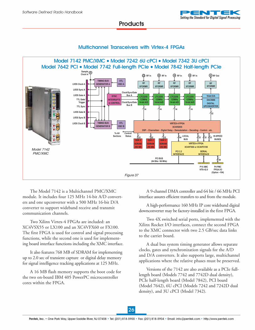
Multichannel Transceivers with Virtex-4 FPGAs
Products
Model 7142PMC/XMC
Figure 37
Model 7142 PMC/XMC ●●●●● Model 7242 6U cPCI ●●●●● Model 7342 3U cPCI
Model 7642 PCI ●●●●● Model 7742 Full-length PCIe ●●●●● Model 7842 Half-length PCIe
The Model 7142 is a Multichannel PMC/XMCmodule. It includes four 125 MHz 14-bit A/D convert-ers and one upconverter with a 500 MHz 16-bit D/Aconverter to support wideband receive and transmitcommunication channels.
Two Xilinx Virtex-4 FPGAs are included: anXC4VSX55 or LX100 and an XC4VFX60 or FX100.The first FPGA is used for control and signal processingfunctions, while the second one is used for implement-ing board interface functions including the XMC interface.
It also features 768 MB of SDRAM for implementingup to 2.0 sec of transient capture or digital delay memoryfor signal intelligence tracking applications at 125 MHz.
A 16 MB flash memory supports the boot code forthe two on-board IBM 405 PowerPC microcontrollercores within the FPGA.
A 9-channel DMA controller and 64 bit / 66 MHz PCIinterface assures efficient transfers to and from the module.
A high-performance 160 MHz IP core wideband digitaldownconverter may be factory-installed in the first FPGA.
Two 4X switched serial ports, implemented with theXilinx Rocket I/O interfaces, connect the second FPGAto the XMC connector with two 2.5 GB/sec data linksto the carrier board.
A dual bus system timing generator allows separateclocks, gates and synchronization signals for the A/Dand D/A converters. It also supports large, multichannelapplications where the relative phases must be preserved.
Versions of the 7142 are also available as a PCIe full-length board (Models 7742 and 7742D dual density),PCIe half-length board (Model 7842), PCI board(Model 7642), 6U cPCI (Models 7242 and 7242D dualdensity), and 3U cPCI (Model 7342).
Pentek, Inc. • One Park Way, Upper Saddle River, NJ 07458 • Tel: (201) 818-5900 • Fax: (201) 818-5904 • Email: [email protected] • http://www.pentek.com
27
Software Defined Radio Handbook
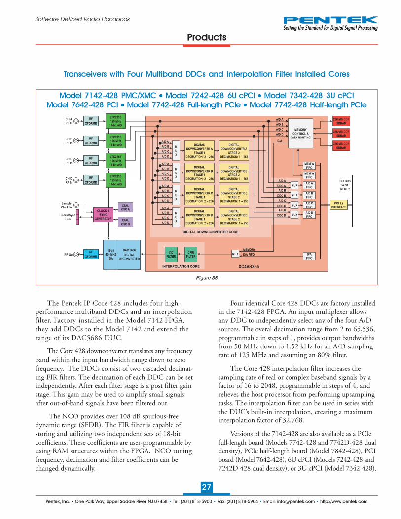
Transceivers with Four Multiband DDCs and Interpolation Filter Installed Cores
Products
Figure 38
.
RF
XFORMR
RF
XFORMR
RF
XFORMR
AD6645
105 MHz
14-bit A/D
CLOCK &
SYNC
GENERATOR
DAC 5686
DIGITAL
UPCONVERTER
16-bit
500 MHZ
D/A
PCI 2.2
INTERFACE
MEMORY
CONTROL &
DATA ROUTING
D/A
FIFO
MUXCFIR
FILTER
CIC
FILTER
MUX
DIGITAL
DOWNCONVERTR A
STAGE 1
DECIMATION: 2 – 256
CH A
RF In
CH B
RF In
RF Out
Sample
Clock In
Clock/Sync
Bus
A/D A
A/D A
A/D B
A/D A
MEMORY
D/A FIFO
PCI BUS
64 bit /
66 MHz
DIGITAL DOWNCONVERTER CORE
INTERPOLATION CORE XC4VSX55
RF
XFORMR
RF
XFORMR
RF
XFORMR
LTC2255
125 MHz
14-bit A/D
CLOCK &
SYNC
GENERATOR
XTAL
OSC A
XTAL
OSC B
DAC 5686
DIGITAL
UPCONVERTER
16-bit
500 MHZ
D/A
PCI 2.2
INTERFACE
LTC2255
125 MHz
14-bit A/D
RF
XFORMR
CH C
RF In
RF
XFORMR
LTC2255
125 MHz
14-bit A/D
RF
XFORMR
CH D
RF In
RF
XFORMR
LTC2255
125 MHz
14-bit A/D
A/D B
A/D C
A/D D
A/D C
A/D D
DIGITAL
DOWNCONVERTR A
STAGE 2
DECIMATION: 1 – 256
DIGITAL
DOWNCONVERTR B
STAGE 1
DECIMATION: 2 – 256
A/D A
A/D B
A/D C
A/D D
DIGITAL
DOWNCONVERTR B
STAGE 2
DECIMATION: 1 – 256
DIGITAL
DOWNCONVERTR C
STAGE 1
DECIMATION: 2 – 256
A/D A
A/D B
A/D C
A/D D
DIGITAL
DOWNCONVERTR C
STAGE 2
DECIMATION: 1 – 256
DIGITAL
DOWNCONVERTR D
STAGE 1
DECIMATION: 2 – 256
A/D A
A/D B
A/D C
A/D D
DIGITAL
DOWNCONVERTR D
STAGE 2
DECIMATION: 1 – 256
DDC A
MUX
A/D B
DDC B
MUX
A/D C
DDC C
MUX
A/D D
DDC D
D/A
M
U
X
M
U
X
M
U
X
M
U
X
MEM W
FIFO
MEM W
FIFO
A/D A
FIFO
A/D B
FIFO
A/D C
FIFO
A/D D
FIFO
256 MB DDR
SDRAM
256 MB DDR
SDRAM
256 MB DDR
SDRAM
Model 7142-428 PMC/XMC ●●●●● Model 7242-428 6U cPCI ●●●●● Model 7342-428 3U cPCI
Model 7642-428 PCI ●●●●● Model 7742-428 Full-length PCIe ●●●●● Model 7742-428 Half-length PCIe
The Pentek IP Core 428 includes four high-performance multiband DDCs and an interpolationfilter. Factory-installed in the Model 7142 FPGA,they add DDCs to the Model 7142 and extend therange of its DAC5686 DUC.
The Core 428 downconverter translates any frequencyband within the input bandwidth range down to zerofrequency. The DDCs consist of two cascaded decimat-ing FIR filters. The decimation of each DDC can be setindependently. After each filter stage is a post filter gainstage. This gain may be used to amplify small signalsafter out-of-band signals have been filtered out.
The NCO provides over 108 dB spurious-freedynamic range (SFDR). The FIR filter is capable ofstoring and utilizing two independent sets of 18-bitcoefficients. These coefficients are user-programmable byusing RAM structures within the FPGA. NCO tuningfrequency, decimation and filter coefficients can bechanged dynamically.
Four identical Core 428 DDCs are factory installedin the 7142-428 FPGA. An input multiplexer allowsany DDC to independently select any of the four A/Dsources. The overal decimation range from 2 to 65,536,programmable in steps of 1, provides output bandwidthsfrom 50 MHz down to 1.52 kHz for an A/D samplingrate of 125 MHz and assuming an 80% filter.
The Core 428 interpolation filter increases thesampling rate of real or complex baseband signals by afactor of 16 to 2048, programmable in steps of 4, andrelieves the host processor from performing upsamplingtasks. The interpolation filter can be used in series withthe DUC’s built-in interpolation, creating a maximuminterpolation factor of 32,768.
Versions of the 7142-428 are also available as a PCIefull-length board (Models 7742-428 and 7742D-428 dualdensity), PCIe half-length board (Model 7842-428), PCIboard (Model 7642-428), 6U cPCI (Models 7242-428 and7242D-428 dual density), or 3U cPCI (Model 7342-428).

Pentek, Inc. • One Park Way, Upper Saddle River, NJ 07458 • Tel: (201) 818-5900 • Fax: (201) 818-5904 • Email: [email protected] • http://www.pentek.com
28
Software Defined Radio Handbook
256-Channel DDC Installed Core with Quad 200 MHz, 16-bit A/D
Products
Figure 39
.
RF
XFORMR
RF
XFORMR
AD6645
105 MHz
14-bit A/D
PCI 2.2
INTERFACE
MUXDIGITAL
DOWNCONVERTR
BANK 1: CH 1 - 64
DECIMATION: 128 - 1024
CH A
RF In
CH B
RF In
Sample
Clock In
Sync Bus
A/D A
A/D BI & Q
PCI BUS
64 bit /
66 MHz
DIGITAL DOWNCONVERTER CORE
XC5VSX95T
RF
XFORMR
RF
XFORMR
ADS5485
200 MHz
16-bit A/D
TIMING BUS
GENERATOR
Clock / Gate /
Sync / PPS
XTAL
OSC
PCI 2.2
INTERFACE
ADS5485
200 MHz
16-bit A/D
RF
XFORMR
CH C
RF In
RF
XFORMR
ADS5485
200 MHz
16-bit A/D
RF
XFORMR
CH D
RF In
RF
XFORMR
ADS5485
200 MHz
16-bit A/D
A/D C
A/D D
DDC BANK 1
MUX
MUX
MUX
M
U
X
M
U
X
M
U
X
M
U
X
A/D A
FIFO
A/D B
FIFO
A/D C
FIFO
A/D D
FIFO
PPS In
TTL In
A/D A
A/D B
A/D C
A/D D
A/D A
A/D B
A/D C
A/D D
A/D A
A/D B
A/D C
A/D D
DIGITAL
DOWNCONVERTR
BANK 2: CH 65 - 128
DECIMATION: 128 - 1024
DIGITAL
DOWNCONVERTR
BANK 3: CH 129 - 192
DECIMATION: 128 - 1024
DIGITAL
DOWNCONVERTR
BANK 4: CH 193 - 256
DECIMATION: 128 - 1024
A/D B
DDC BANK 2
A/D C
DDC BANK 3
A/D D
DDC BANK 4
I & Q
I & Q
I & Q
The Model 7151 PMC module is a 4-channel high-speed digitizer with a factory-installed 256-channelDDC core. The front end of the module accepts fourRF inputs and transformer-couples them into four16-bit A/D converters running at 200 MHz. Thedigitized output signals pass to a Virtex-5 FPGA forrouting, formatting and DDC signal processing.
The Model 7151 employs an advanced FPGA-baseddigital downconverter engine consisting of four identical64-channel DDC banks. Four independently controllableinput multiplexers select one of the four A/Ds as theinput source for each DDC bank. Each of the 256 DDCshas an independent 32-bit tuning frequency setting.
All of the 64 channels within a bank share a commondecimation setting that can range from 128 to 1024,programmable in steps of 64. For example, with a samplingrate of 200 MHz, the available output bandwidthsrange from 156.25 kHz to 1.25 MHz. Each 64-channelbank can have its own unique decimation setting
supporting as many as four different output bandwidthsfor the board.
The decimating filter for each DDC bank accepts aunique set of user-supplied 18-bit coefficients. The 80%default filters deliver an output bandwidth of 0.8*ƒs/N,where N is the decimation setting. The rejection ofadjacent-band components within the 80% output band-width is better than 100 dB.
Each DDC delivers a complex output streamconsisting of 24-bit I + 24-bit Q samples. Any numberof channels can be enabled within each bank, selectablefrom 0 to 64. Each bank includes an output sampleinterleaver that delivers a channel-multiplexed stream forall enabled channels within the bank.
Versions of the 7151 are also available as a PCIefull-length board (Models 7751 and 7751D dual density),PCIe half-length board (Model 7851), PCI board(Model 7651), 6U cPCI (Models 7251 and 7251D dualdensity), or 3U cPCI (Model 7351).
Model 7151 PMC ●●●●● Model 7251 6U cPCI ●●●●● Model 7351 3U cPCI
Model 7651 PCI ●●●●● Model 7751 Full-length PCIe ●●●●● Model 7851 Half-length PCIe

Pentek, Inc. • One Park Way, Upper Saddle River, NJ 07458 • Tel: (201) 818-5900 • Fax: (201) 818-5904 • Email: [email protected] • http://www.pentek.com
29
Software Defined Radio Handbook
32-Channel DDC Installed Core with Quad 200 MHz, 16-bit A/D
Products
Figure 40
.
RF
XFORMR
RF
XFORMR
AD6645
105 MHz
14-bit A/D
PCI 2.2
INTERFACE
MUXDIGITAL
DOWNCONVERTR
BANK 1: CH 1 - 8
DEC: 16 - 8192
CH A
RF In
CH B
RF In
Sample
Clock In
Sync Bus
A/D A
A/D BI & Q
PCI BUS
64 bit /
66 MHz
DIGITAL DOWNCONVERTER CORE
XC5VSX95T
RF
XFORMR
RF
XFORMR
ADS5485
200 MHz
16-bit A/D
TIMING BUS
GENERATOR
Clock / Gate /
Sync / PPS
XTAL
OSC
PCI 2.2
INTERFACE
ADS5485
200 MHz
16-bit A/D
RF
XFORMR
CH C
RF In
RF
XFORMR
ADS5485
200 MHz
16-bit A/D
RF
XFORMR
CH D
RF In
RF
XFORMR
ADS5485
200 MHz
16-bit A/D
A/D C
A/D D
BANK 1
MUX
MUX
MUX
M
U
X
M
U
X
M
U
X
M
U
X
A/D A
FIFO
A/D B
FIFO
A/D C
FIFO
A/D D
FIFO
PPS In
TTL In
A/D A
A/D B
A/D C
A/D D
A/D A
A/D B
A/D C
A/D D
A/D A
A/D B
A/D C
A/D D
DIGITAL
DOWNCONVERTR
BANK 2: CH 9 - 16
DEC: 16 - 8192
DIGITAL
DOWNCONVERTR
BANK 3: CH 17 - 24
DEC: 16 - 8192
DIGITAL
DOWNCONVERTR
BANK 4: CH 25 - 32
DEC: 16 - 8192
A/D B
BANK 2
A/D C
BANK 3
A/D D
BANK 4
8 x 4
CHANNEL
SUMMATION
POWER
METER &
THRESHOLD
DETECT
POWER
METER &
THRESHOLD
DETECT
POWER
METER &
THRESHOLD
DETECT
POWER
METER &
THRESHOLD
DETECT
A/D B
I & Q
I & Q
I & Q
SUM
Model 7152 PMC ●●●●● Model 7252 6U cPCI ●●●●● Model 7352 3U cPCI
Model 7652 PCI ●●●●● Model 7752 Full-length PCIe ●●●●● Model 7852 Half-length PCIe
The Model 7152 PMC module is a 4-channel high-speed digitizer with a factory-installed 32-channel DDCcore. The front end of the module accepts four RFinputs and transformer-couples them into four16-bit A/D converters running at 200 MHz. Thedigitized output signals pass to a Virtex-5 FPGA forrouting, formatting and DDC signal processing.
The Model 7152 employs an advanced FPGA-baseddigital downconverter engine consisting of four identical8-channel DDC banks. Four independently controllableinput multiplexers select one of the four A/Ds as theinput source for each DDC bank. Each of the 32 DDCshas an independent 32-bit tuning frequency setting.
All of the 8 channels within a bank share a commondecimation setting that can range from 16 to 8192,programmable in steps of 8. For example, with a samplingrate of 200 MHz, the available output bandwidths rangefrom 19.53 kHz to 10.0 MHz. Each 8-channel bank can
have its own unique decimation setting supporting asmany as four different output bandwidths for the board.
The decimating filter for each DDC bank accepts a uniqueset of user-supplied 18-bit coefficients. The 80% default filtersdeliver an output bandwidth of 0.8*ƒs/N, where N is thedecimation setting. The rejection of adjacent-band componentswithin the 80% output band-width is better than 100 dB.
Each DDC delivers a complex output stream consist-ing of 24-bit I + 24-bit Q samples. Any number of channelscan be enabled within each bank, selectable from 0 to 8.Each bank includes an output sample interleaver thatdelivers a channel-multiplexed stream for all enabledchannels within the bank. Gain and phase control, powermeters and threshold detectors are included.
Versions of the 7152 are also available as a PCIe full-length board (Models 7752 and 7752D dual density), PCIehalf-length board (Model 7852), PCI board (Model 7652),6U cPCI (Models 7252 and 7252D dual density), or 3UcPCI (Model 7352).
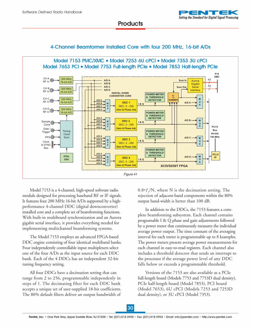
Pentek, Inc. • One Park Way, Upper Saddle River, NJ 07458 • Tel: (201) 818-5900 • Fax: (201) 818-5904 • Email: [email protected] • http://www.pentek.com
30
Software Defined Radio Handbook
4-Channel Beamformer Installed Core with four 200 MHz, 16-bit A/Ds
Products
Figure 41
Model 7153 is a 4-channel, high-speed software radiomodule designed for processing baseband RF or IF signals.It features four 200 MHz 16-bit A/Ds supported by a high-performance 4-channel DDC (digital downconverter)installed core and a complete set of beamforming functions.With built-in multiboard synchronization and an Auroragigabit serial interface, it provides everything needed forimplementing multichannel beamforming systems.
The Model 7153 employs an advanced FPGA-basedDDC engine consisting of four identical multiband banks.Four independently controllable input multiplexers selectone of the four A/Ds as the input source for each DDCbank. Each of the 4 DDCs has an independent 32-bittuning frequency setting.
All four DDCs have a decimation setting that canrange from 2 to 256, programmable independenly insteps of 1. The decimating filter for each DDC bankaccepts a unique set of user-supplied 18-bit coefficients.The 80% default filters deliver an output bandwidth of
0.8*ƒs/N, where N is the decimation setting. Therejection of adjacent-band components within the 80%output band-width is better than 100 dB.
In addition to the DDCs, the 7153 features a com-plete beamforming subsystem. Each channel containsprogramable I & Q phase and gain adjustments followedby a power meter that continuously measures the individualaverage power output. The time constant of the averaginginterval for each meter is programmable up to 8 ksamples.The power meters present average power measurements foreach channel in easy-to-read registers. Each channel alsoincludes a threshold detector that sends an interrupt tothe processor if the average power level of any DDCfalls below or exceeds a programmable threshold.
Versions of the 7153 are also available as a PCIefull-length board (Models 7753 and 7753D dual density),PCIe half-length board (Model 7853), PCI board(Model 7653), 6U cPCI (Models 7253 and 7253Ddual density), or 3U cPCI (Model 7353).
Model 7153 PMC/XMC ●●●●● Model 7253 6U cPCI ●●●●● Model 7353 3U cPCI
Model 7653 PCI ●●●●● Model 7753 Full-length PCIe ●●●●● Model 7853 Half-length PCIe
DDC 1
DEC: 2 - 256
Gain & Phase Adj
A/D A
A/D B I & Q
PCI-X
I/F
A/D C
A/D D
MU
X
200 MHz
16-bit A/D
200 MHz
16-bit A/D
200 MHz
16-bit A/D
200 MHz
16-bit A/D
CH B
RF In
CH A
RF In
CH D
RF In
CH C
RF In
Sample
Clock
Clock
& SYNC
Bus
Timing
Clock
Sync
Gate /
Trigger
PPS
XTAL
OSC
DDC 2
DEC: 2 - 256
Gain & Phase Adj
DDC 3
DEC: 2 - 256
Gain & Phase Adj
DDC 4
DEC: 2 - 256
Gain & Phase Adj
M
U
X
M
UX
M
U
X
MU
X
A/D A
A/D A
A/D B
A/D C
A/D D
M
UX
A/D A
A/D B
A/D C
A/D D
MU
X
A/D A
A/D B
A/D C
A/D D
M
UX
PCI-X
Bus
64-bits
100 MHz
I & Q
I & Q
I & Q
POWER METER
& THRESHOLD
DETECTOR
POWER METER
& THRESHOLDDETECTOR
POWER METER
& THRESHOLDDETECTOR
POWER METER
& THRESHOLD
DETECTOR
�SUMMER
DIGITAL DOWN
CONVERTER CORE
XC5VSX50T FPGA
A/D A
A/D B
A/D C
A/D D
A/D B
A/D C
A/D D
Aurora
Gigabit
Serial
Interface
Sum In
Sum Out
P15
XMC
4X
4X

Pentek, Inc. • One Park Way, Upper Saddle River, NJ 07458 • Tel: (201) 818-5900 • Fax: (201) 818-5904 • Email: [email protected] • http://www.pentek.com
31
Software Defined Radio Handbook
Products
Dual SDR Transceivers with 400 MHz A/D, 800 MHz D/A, and Virtex-5 FPGAs
Model 7156PMC/XMC
RF In
14
ADS5474
400 MHz
14-bit A/D
RF
XFORMR
RF In
14
ADS5474
400 MHz
14-bit A/D
RF
XFORMR
TIMING BUS
GENERATOR
Clock/ Sync /
Gate / PPS
Sample Clock In
TTL Gate / Trig
A/D Clock Bus
TTL Sync / PPS
Sample Clk
Sync Clk
Gate A
Gate B
Sync
PPS
PPS In
PROCESSING FPGA
VIRTEX –5: LX50T, SX50T, SX95T or FX100TTo All
Sections
Control/
Status
VCXO
GTP GTP GTP
INTERFACE FPGA
VIRTEX-5: LX30T, SX50T or FX70T
PCI-X BUS
(64 Bits
100 MHz)
P15 XMC
VITA 42.x
(PCIe, etc.)
P4 PMC
FPGA
I/O
64
32
4X
4X
4X4X
GTP
PCI-X GTP
1632 32
DDR 2
SDRAM
512 MB
DDR 2
SDRAM
512 MB
FLASH
32 MB
32
LVDS
LVDS
Timing Bus
D/A Clock Bus
32
RF
XFORMR
RF
XFORMR
RF Out RF Out
DIGITAL UPCONVERTER
800 MHz
16-bit D/A
800 MHz
16-bit D/A
64
Model 7156 is a dual high-speed data convertersuitable for connection as the HF or IF input of acommunications system. It features two 400 MHz 14-bitA/Ds, a DUC with two 800 MHz 16-bit D/As, andtwo Virtex-5 FPGAs. Model 7156 uses the popularPMC format and supports the VITA 42 XMC standardfor switched fabric interfaces.
The Model 7156 architecture includes two Virtex-5FPGAs. The first FPGA is used primarily for signalprocessing while the second one is dedicated to boardinterfaces. All of the board’s data and control paths areaccessible by the FPGAs, enabling factory installedfunctions such as data multiplexing, channel selection, datapacking, gating, triggering and SDRAM memory control.
Two independent 512 MB banks of DDR2 SDRAMare available to the signal processing FPGA. Built-inmemory functions include an A/D data transient capturemode with pre- and post-triggering. All memory bankscan be easily accessed through the PCI-X interface.
A high-performance IP core wideband DDC may befactory-installed in the processing FPGA.
A 5-channel DMA controller and 64 bit/100 MHz PCI-X interface assures efficient transfers to and from the module.
Two 4X switched serial ports implemented with theXilinx Rocket I/O interfaces, connect the FPGA to theXMC connector with two 2.5 GB/sec data links to thecarrier board.
A dual bus system timing generator allows separateclocks, gates and synchronization signals for the A/Dand D/A converters. It also supports large, multichannelapplications where the relative phases must be preserved.
Versions of the 7156 are also available as a PCIe full-length board (Models 7756 and 7756D dual density),PCIe half-length board (Model 7856), PCI board(Model 7656), 6U cPCI (Models 7256 and 7256D dualdensity), or 3U cPCI (Model 7356). All these productshave similar features.
Figure 42
Model 7156 PMC/XMC ●●●●● Model 7256 6U cPCI ●●●●● Model 7356 3U cPCI
Model 7656 PCI ●●●●● Model 7756 Full-length PCIe ●●●●● Model 7856 Half-length PCIe

Pentek, Inc. • One Park Way, Upper Saddle River, NJ 07458 • Tel: (201) 818-5900 • Fax: (201) 818-5904 • Email: [email protected] • http://www.pentek.com
32
Software Defined Radio Handbook
Model 7158 is a dual high-speed data convertersuitable for connection as the HF or IF input of acommunications system. It features two 500 MHz 12-bitA/Ds, a digital upconverter with two 800 MHz 16-bitD/As, and two Virtex-5 FPGAs. Model 7158 uses thepopular PMC format and supports the VITA 42 XMCstandard for switched fabric interfaces.
The Model 7158 architecture includes two Virtex-5FPGAs. The first FPGA is used primarily for signalprocessing while the second one is dedicated to boardinterfaces. All of the board’s data and control paths areaccessible by the FPGAs, enabling factory installedfunctions such as data multiplexing, channel selection, datapacking, gating, triggering and SDRAM memory control.
Two independent 256 MB banks of DDR2 SDRAMare available to the signal processing FPGA. Built-inmemory functions include an A/D data transient capturemode with pre- and post-triggering. All memory bankscan be easily accessed through the PCI-X interface.
A 5-channel DMA controller and 64 bit / 100 MHzPCI-X interface assures efficient transfers to and from themodule.
Two 4X switched serial ports implemented with theXilinx Rocket I/O interfaces, connect the FPGA to theXMC connector with two 2.5 GB/sec data links to thecarrier board.
A dual bus system timing generator allows separateclocks, gates and synchronization signals for the A/Dand D/A converters. It also supports large, multichannelapplications where the relative phases must be preserved.
Versions of the 7158 are also available as a PCIe full-length board (Models 7758 and 7758D dual density),PCIe half-length board (Model 7858), PCI board(Model 7658), 6U cPCI (Models 7258 and 7258D dualdensity), or 3U cPCI (Model 7358). All these productshave similar features.
Dual SDR Transceivers with 500 MHz A/D, 800 MHz D/A, and Virtex-5 FPGAs
Model 7158 PMC/XMC ●●●●● Model 7258 6U cPCI ●●●●● Model 7358 3U cPCI
Model 7658 PCI ●●●●● Model 7758 Full-length PCIe ●●●●● Model 7858 Half-length PCIe
Figure 43
Products
Model 7158PMC/XMC
RF In
14
ADS5463
500 MHz
12-bit A/D
RF
XFORMR
RF In
14
ADS5463
500 MHz
12-bit A/D
RF
XFORMR
TIMING BUS
GENERATOR
Clock/ Sync /
Gate / PPS
Sample Clock /
Reference Clock In
TTL Gate / Trig
A/D Clock Bus
TTL Sync / PPS
Sample Clk
Sync Clk
Gate A
Gate B
Sync
PPS
PPS In
PROCESSING FPGA
VIRTEX –5: LX50T, LX155T, SX50T, SX95T or FX100TTo All
Sections
Control/
Status
VCXO
GTP GTP GTP
INTERFACE FPGA
VIRTEX-5: LX30T, SX50T or FX70T
PCI-X BUS
(64 Bits
100 MHz)
P15 XMC
VITA 42.x
(PCIe, etc.)
P4 PMC
FPGA
I/O
64
32
4X
4X
4X4X
GTP
PCI-X GTP
1632 32
DDR 2
SDRAM
256 MB
DDR 2
SDRAM
256 MB
FLASH
32 MB
32
LVDS
LVDS
Timing Bus
D/A Clock Bus
32
RF
XFORMR
RF
XFORMR
RF Out RF Out
DIGITAL UPCONVERTER
800 MHz
16-bit D/A
800 MHz
16-bit D/A
64
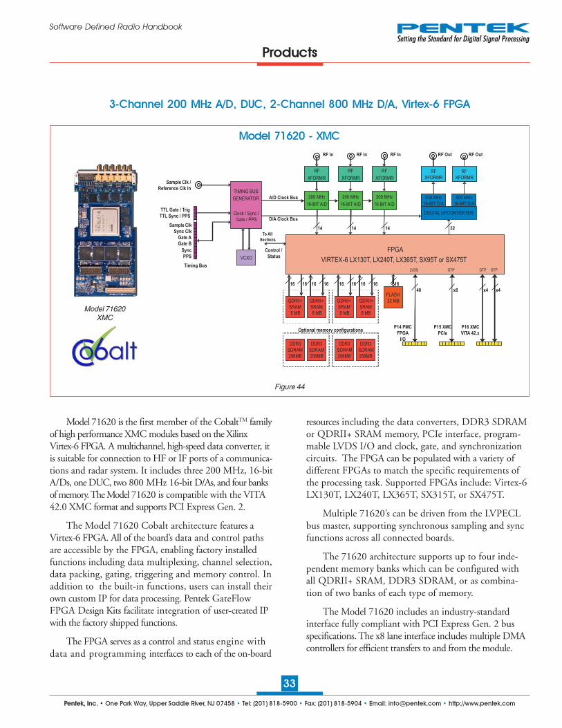
Pentek, Inc. • One Park Way, Upper Saddle River, NJ 07458 • Tel: (201) 818-5900 • Fax: (201) 818-5904 • Email: [email protected] • http://www.pentek.com
33
Software Defined Radio Handbook
3-Channel 200 MHz A/D, DUC, 2-Channel 800 MHz D/A, Virtex-6 FPGA
Model 71620 - XMC
Figure 44
Products
Model 71620XMC
TIMING BUS
GENERATOR
Clock / Sync /
Gate / PPS
Sample Clk /
Reference Clk In
Sample Clk
TTL Gate / Trig
TTL Sync / PPS
Sync Clk
Gate A
Gate B
Sync
PPS
Timing Bus
VCXO
DIGITAL UPCONVERTER
800 MHz
16-BIT D/A
800 MHz
16-BIT D/A
RF
XFORMR
RF
XFORMR
RF OutRF Out
RF
XFORMR
200 MHz
16-BIT A/D
RF In
200 MHz
16-BIT A/D
RF
XFORMR
RF In
321414
RF
XFORMR
RF In
200 MHz
16-BIT A/D
14
A/D Clock Bus
D/A Clock Bus
FPGA
VIRTEX-6 LX130T, LX240T, LX365T, SX95T or SX475T
Control /
Status
To All
Sections
FLASH
32 MB
16
40
P14 PMC
FPGA
I/O
x8
P15 XMC
PCIe
x4 x4
P16 XMC
VITA 42.x
16
QDRII+
SRAM
8 MB
16 16
QDRII+
SRAM
8 MB
16 16
QDRII+
SRAM
8 MB
16 16
QDRII+
SRAM
8 MB
16
DDR3
SDRAM
256MB
DDR3
SDRAM
256MB
DDR3
SDRAM
256MB
DDR3
SDRAM
256MB
Optional memory configurations
LVDS GTP GTP GTP
Model 71620 is the first member of the CobaltTM familyof high performance XMC modules based on the XilinxVirtex-6 FPGA. A multichannel, high-speed data converter, itis suitable for connection to HF or IF ports of a communica-tions and radar system. It includes three 200 MHz, 16-bitA/Ds, one DUC, two 800 MHz 16-bit D/As, and four banksof memory. The Model 71620 is compatible with the VITA42.0 XMC format and supports PCI Express Gen. 2.
The Model 71620 Cobalt architecture features aVirtex-6 FPGA. All of the board’s data and control pathsare accessible by the FPGA, enabling factory installedfunctions including data multiplexing, channel selection,data packing, gating, triggering and memory control. Inaddition to the built-in functions, users can install theirown custom IP for data processing. Pentek GateFlowFPGA Design Kits facilitate integration of user-created IPwith the factory shipped functions.
The FPGA serves as a control and status engine withdata and programming interfaces to each of the on-board
resources including the data converters, DDR3 SDRAMor QDRII+ SRAM memory, PCIe interface, program-mable LVDS I/O and clock, gate, and synchronizationcircuits. The FPGA can be populated with a variety ofdifferent FPGAs to match the specific requirements ofthe processing task. Supported FPGAs include: Virtex-6LX130T, LX240T, LX365T, SX315T, or SX475T.
Multiple 71620’s can be driven from the LVPECLbus master, supporting synchronous sampling and syncfunctions across all connected boards.
The 71620 architecture supports up to four inde-pendent memory banks which can be configured withall QDRII+ SRAM, DDR3 SDRAM, or as combina-tion of two banks of each type of memory.
The Model 71620 includes an industry-standardinterface fully compliant with PCI Express Gen. 2 busspecifications. The x8 lane interface includes multiple DMAcontrollers for efficient transfers to and from the module.
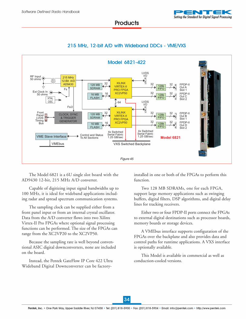
Pentek, Inc. • One Park Way, Upper Saddle River, NJ 07458 • Tel: (201) 818-5900 • Fax: (201) 818-5904 • Email: [email protected] • http://www.pentek.com
34
Software Defined Radio Handbook
215 MHz, 12-bit A/D with Wideband DDCs - VME/VXS
The Model 6821 is a 6U single slot board with theAD9430 12-bit, 215 MHz A/D converter.
Capable of digitizing input signal bandwidths up to100 MHz, it is ideal for wideband applications includ-ing radar and spread spectrum communication systems.
The sampling clock can be supplied either from afront panel input or from an internal crystal oscillator.Data from the A/D converter flows into two XilinxVirtex-II Pro FPGAs where optional signal processingfunctions can be performed. The size of the FPGAs canrange from the XC2VP20 to the XC2VP50.
Because the sampling rate is well beyond conven-tional ASIC digital downconverters, none are includedon the board.
Instead, the Pentek GateFlow IP Core 422 UltraWideband Digital Downconverter can be factory-
installed in one or both of the FPGAs to perform thisfunction.
Two 128 MB SDRAMs, one for each FPGA,support large memory applications such as swingingbuffers, digital filters, DSP algorithms, and digital delaylines for tracking receivers.
Either two or four FPDP-II ports connect the FPGAsto external digital destinations such as processor boards,memory boards or storage devices.
A VMEbus interface supports configuration of theFPGAs over the backplane and also provides data andcontrol paths for runtime applications. A VXS interfaceis optionally available.
This Model is available in commercial as well asconduction-cooled versions.
Figure 45
Model 6821-422
Products
128kFIFO
FPDP-IIOut CSlot 2
FPDP-IIOut BSlot 1
32 32
128kFIFO
FPDP-IIOut DSlot 2
32 32
128kFIFO
FPDP-IIOut ASlot 1
32 32
32 32
128kFIFO
16 MB
FLASH
16
128 MB
SDRAM
32
16 MB
FLASH
16
128 MB
SDRAM
32
XILINX
VIRTEX-II
PRO FPGA
XC2VP50
64
XILINX
VIRTEX-II
PRO FPGA
XC2VP50
215 MHz
12-Bit A/D
AD9430
RF Input50 ohms
VMEbus
VME Slave Interface
XTAL
OSC
Ext Clock In50 ohms
CLOCK, SYNC
& TRIGGER
GENERATOR
Fs/2
FrontPanelLVDS
TimingBus
Control and StatusTo All Sections
Fs
Model 6821
4x SwitchedSerial Fabric1.25 GB/sec
VXS Switched Backplane
4x SwitchedSerial Fabric1.25 GB/sec
LVDSI/O
LVDSI/O
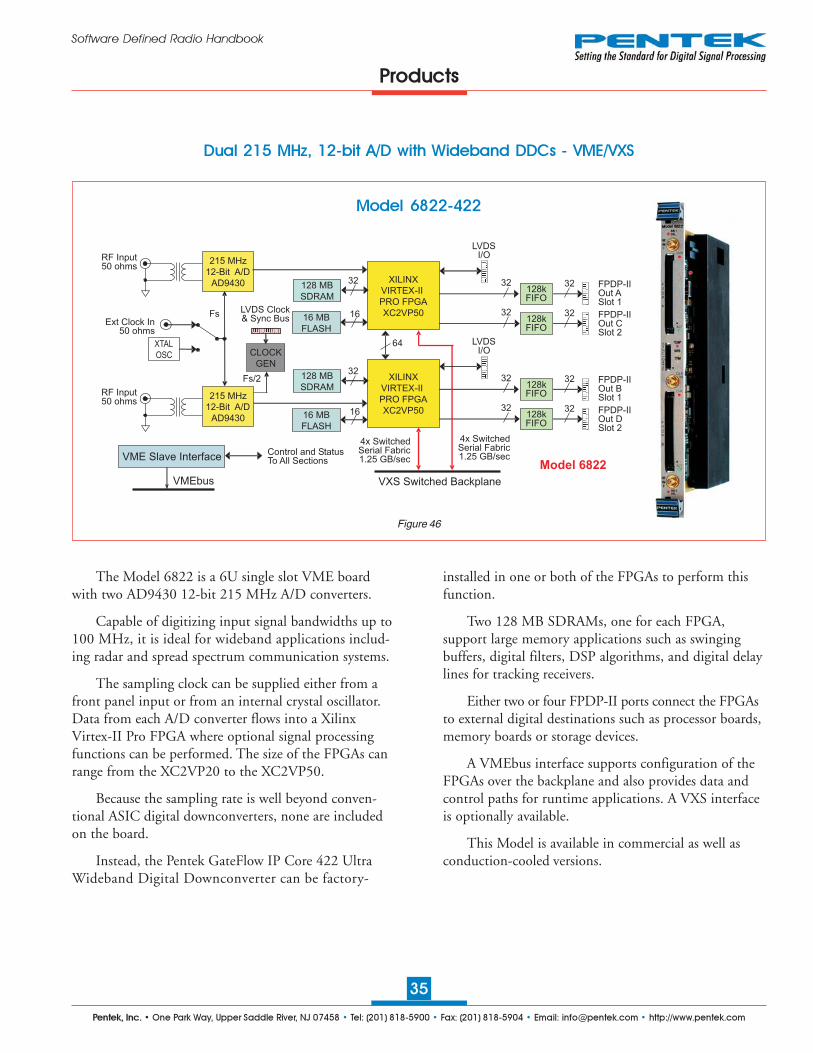
Pentek, Inc. • One Park Way, Upper Saddle River, NJ 07458 • Tel: (201) 818-5900 • Fax: (201) 818-5904 • Email: [email protected] • http://www.pentek.com
35
Software Defined Radio Handbook
Dual 215 MHz, 12-bit A/D with Wideband DDCs - VME/VXS
The Model 6822 is a 6U single slot VME boardwith two AD9430 12-bit 215 MHz A/D converters.
Capable of digitizing input signal bandwidths up to100 MHz, it is ideal for wideband applications includ-ing radar and spread spectrum communication systems.
The sampling clock can be supplied either from afront panel input or from an internal crystal oscillator.Data from each A/D converter flows into a XilinxVirtex-II Pro FPGA where optional signal processingfunctions can be performed. The size of the FPGAs canrange from the XC2VP20 to the XC2VP50.
Because the sampling rate is well beyond conven-tional ASIC digital downconverters, none are includedon the board.
Instead, the Pentek GateFlow IP Core 422 UltraWideband Digital Downconverter can be factory-
installed in one or both of the FPGAs to perform thisfunction.
Two 128 MB SDRAMs, one for each FPGA,support large memory applications such as swingingbuffers, digital filters, DSP algorithms, and digital delaylines for tracking receivers.
Either two or four FPDP-II ports connect the FPGAsto external digital destinations such as processor boards,memory boards or storage devices.
A VMEbus interface supports configuration of theFPGAs over the backplane and also provides data andcontrol paths for runtime applications. A VXS interfaceis optionally available.
This Model is available in commercial as well asconduction-cooled versions.
Model 6822-422
Figure 46
Products
FPDP-IIOut ASlot 1
32 32
32 32
128kFIFO
XILINX
VIRTEX-II
PRO FPGA
XC2VP50
FPDP-IIOut BSlot 1
32XILINX
VIRTEX-II
PRO FPGA
XC2VP50
32
128kFIFO
FPDP-IIOut DSlot 2
32 32
4x SwitchedSerial Fabric1.25 GB/sec
4x SwitchedSerial Fabric1.25 GB/sec
VXS Switched Backplane
215 MHz
12-Bit A/D
AD9430
RF Input50 ohms
XTAL
OSC
Ext Clock In50 ohms
CLOCK
GEN
LVDS Clock& Sync Bus
Fs
215 MHz
12-Bit A/D
AD9430
RF Input50 ohms
VMEbus
VME Slave InterfaceControl and StatusTo All Sections
Fs/2
16 MB
FLASH
16
64
128 MB
SDRAM
32
16 MB
FLASH
16
128 MB
SDRAM
32
Model 6822
128kFIFO
LVDSI/O
128kFIFO
FPDP-IIOut CSlot 2
LVDSI/O
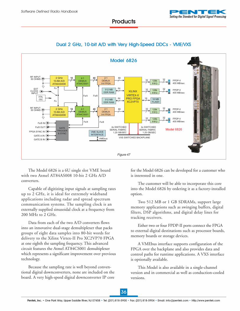
Pentek, Inc. • One Park Way, Upper Saddle River, NJ 07458 • Tel: (201) 818-5900 • Fax: (201) 818-5904 • Email: [email protected] • http://www.pentek.com
36
Software Defined Radio Handbook
Dual 2 GHz, 10-bit A/D with Very High-Speed DDCs - VME/VXS
The Model 6826 is a 6U single slot VME boardwith two Atmel AT84AS008 10-bit 2 GHz A/Dconverters.
Capable of digitizing input signals at sampling ratesup to 2 GHz, it is ideal for extremely widebandapplications including radar and spread spectrumcommunication systems. The sampling clock is anexternally supplied sinusoidal clock at a frequency from200 MHz to 2 GHz.
Data from each of the two A/D converters flowsinto an innovative dual-stage demultiplexer that packsgroups of eight data samples into 80-bit words fordelivery to the Xilinx Virtex-II Pro XC2VP70 FPGAat one eighth the sampling frequency. This advancedcircuit features the Atmel AT84CS001 demultiplexerwhich represents a significant improvement over previoustechnology.
Because the sampling rate is well beyond conven-tional digital downconverters, none are included on theboard. A very high-speed digital downconverter IP core
Model 6826
Products
Figure 47
for the Model 6826 can be developed for a customer whois interested in one.
The customer will be able to incorporate this coreinto the Model 6826 by ordering it as a factory-installedoption.
Two 512 MB or 1 GB SDRAMs, support largememory applications such as swinging buffers, digitalfilters, DSP algorithms, and digital delay lines fortracking receivers.
Either two or four FPDP-II ports connect the FPGAto external digital destinations such as processor boards,memory boards or storage devices.
A VMEbus interface supports configuration of theFPGA over the backplane and also provides data andcontrol paths for runtime applications. A VXS interfaceis optionally available.
This Model is also available in a single-channelversion and in commercial as well as conduction-cooledversions.
4:1
DEMUX
AT84CS001
40 2:1
DEMUX
V4 FPGA
10
40 2:1
DEMUX
V4 FPGA
10 4:1
DEMUX
AT84CS001
16 MB
FLASH
16
VMEbus
VME SLAVE
INTERFACE
Model 6826
128k
FIFO
FPDP-II
400 MB/sec
32 32
128k
FIFO
32 FPDP-II
400 MB/sec
32
128k
FIFO
FPDP-II
400 MB/sec
32 32
128k
FIFO
32 FPDP-II
400 MB/sec
32
VXS SWITCHED BACKPLANE
4x SWITCHED
SERIAL FABRIC
1.25 GB/SEC
4x SWITCHED
SERIAL FABRIC
1.25 GB/SEC
512 MB
DDR RAM
64
512 MB
DDR RAM
64
XILINX
VIRTEX-II
PRO FPGA
XC2VP70
80
80
4:1
DEMUX
AT84CS001
40 2:1
DEMUX
V4 FPGA
10
40 2:1
DEMUX
V4 FPGA
10 4:1
DEMUX
AT84CS001
2 GHz
10-Bit A/D
AT84AS008
RF INPUT50 OHMS
XTAL
OSC
Fs
2 GHz
10-Bit A/D
AT84AS008
RF INPUT50 OHMS
Fs
EXTCLOCKINPUT
GATE
TRIGGER
& SYNC
Fs/4
Fs/4 Fs/8
Fs/8
Fs/8 IN
Fs/8 OUT
FPGA SYNC IN
GATE A IN
GATE B IN

Pentek, Inc. • One Park Way, Upper Saddle River, NJ 07458 • Tel: (201) 818-5900 • Fax: (201) 818-5904 • Email: [email protected] • http://www.pentek.com
37
Software Defined Radio Handbook
Products
Figure 48
Model 6890 - VME
2.2 GHz Clock, Sync and Gate Distribution Board
BUFFER1:2
BUFFER1:2
BUFFER1:2
PROGDELAY
PROGDELAY
MUX2:1
MUX2:1
FrontPanelSync
Output
FrontPanelClock
Output
FrontPanelGate
Output
Ch 1
Ch 1
Ch 1
Ch 2
Ch 2
Ch 2
Ch 3
Ch 3
Ch 3
Ch 4
Ch 4
Ch 4
Ch 5
Ch 5
Ch 5
Ch 6
Ch 6
Ch 6
Ch 7
Ch 7
Ch 7
Ch 8
Ch 8
Ch 8
LVPECLBUFFER
1:8
LVPECLBUFFER
1:8
POWERSPLITTER
1:8
POWERSPLITTER
1:2
TTL / PECLSELECTOR
TTL / PECLSELECTOR
TTL / PECLSELECTOR
TTL / PECLSELECTOR
GATECONTROL
SYNCCONTROL
FrontPanelClockInput
FrontPanelGateInput
FrontPanelSyncInput
FrontPanelGate
Enable
FrontPanelSync
Enable REG
REG
Model 6890VME
Model 6890 Clock, Sync and Gate DistributionBoard synchronizes multiple Pentek I/O boards within asystem. It enables synchronous sampling and timingfor a wide range of multichannel high-speed dataacquisition, DSP and software radio applications. Upto eight boards can be synchronized using the 6890,each receiving a common clock of up to 2.2 GHz alongwith timing signals that can be used for synchronizing,triggering and gating functions.
Clock signals are applied from an external sourcesuch as a high performance sine wave generator. Gateand sync signals can come from an external source, orfrom one supported board set to act as the master.
The 6890 accepts clock input at +10 dBm to +14 dBmwith a frequency range from 800 MHz to 2.2 GHz anduses a 1:2 power splitter to distribute the clock. The firstoutput of this power splitter sends the clock signal to a1:8 splitter for distribution to up to eight boards usingSMA connectors. The second output of the 1:2 power
splitter feeds a 1:2 buffer which distributes the clocksignal to both the gate and synchronization circuits.
The 6890 features separate inputs for gate/triggerand sync signals with user-selectable polarity. Each ofthese inputs can be TTL or LVPECL. Separate GateEnable and Sync Enable inputs allow the user to enableor disable these circuits using an external signal.
A programmable delay allows the user to maketiming adjustments on the gate and sync signals beforethey are sent to an LVPECL buffer. A bank of eightMMCX connectors at the output of each buffer deliverssignals to up to eight boards.
A 2:1 multiplexer in each circuit allows the gate/trigger and sync signals to be registered with the inputclock signal before output, if desired.
Sets of input and output cables for two to eightboards are available from Pentek.
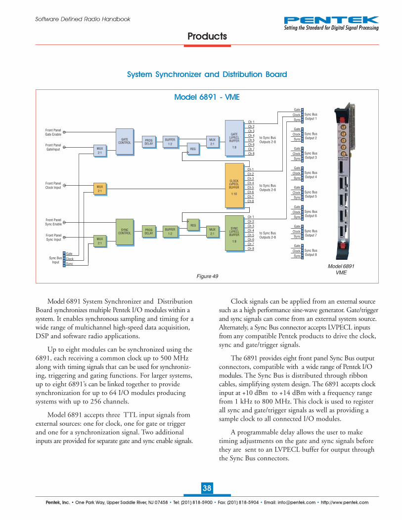
Pentek, Inc. • One Park Way, Upper Saddle River, NJ 07458 • Tel: (201) 818-5900 • Fax: (201) 818-5904 • Email: [email protected] • http://www.pentek.com
38
Software Defined Radio Handbook
Products
Figure 49
System Synchronizer and Distribution Board
Model 6891 - VME
BUFFER1:2
BUFFER1:2
PROGDELAY
PROGDELAY
MUX2:1
MUX2:1
Ch 1
Ch 1
Ch 1
Ch 2
Ch 2
Ch 2
Ch 3
Ch 3
Ch 3
Ch 4
Ch 4
Ch 4
Ch 5
Ch 5
Ch 5
Ch 6
Ch 6
Ch 6
Ch 7
Ch 7
Ch 7
Ch 8
Ch 8
Ch 8
SYNCLVPECLBUFFER
1:8
GATELVPECLBUFFER
1:8
CLOCKLVPECLBUFFER
1:10
GATECONTROL
Front PanelClock Input
Front PanelGateInput
Front PanelSync Input
Front PanelGate Enable
Front PanelSync Enable REG
REG
Gate
SyncClockSync Bus
Input
MUX2:1
MUX2:1
MUX2:1
SYNCCONTROL
Gate
SyncClock Sync Bus
Output 8
Gate
SyncClock Sync Bus
Output 7
Gate
SyncClock Sync Bus
Output 6
Gate
SyncClock Sync Bus
Output 5
Gate
SyncClock Sync Bus
Output 4
Gate
SyncClock Sync Bus
Output 3
Gate
SyncClock Sync Bus
Output 2
Gate
SyncClock Sync Bus
Output 1
to Sync BusOutputs 2-8
to Sync BusOutputs 2-8
to Sync BusOutputs 2-8
Model 6891VME
Model 6891 System Synchronizer and DistributionBoard synchronizes multiple Pentek I/O modules within asystem. It enables synchronous sampling and timing for awide range of multichannel high-speed data acquisition,DSP and software radio applications.
Up to eight modules can be synchronized using the6891, each receiving a common clock up to 500 MHzalong with timing signals that can be used for synchroniz-ing, triggering and gating functions. For larger systems,up to eight 6891’s can be linked together to providesynchronization for up to 64 I/O modules producingsystems with up to 256 channels.
Model 6891 accepts three TTL input signals fromexternal sources: one for clock, one for gate or triggerand one for a synchronization signal. Two additionalinputs are provided for separate gate and sync enable signals.
Clock signals can be applied from an external sourcesuch as a high performance sine-wave generator. Gate/triggerand sync signals can come from an external system source.Alternately, a Sync Bus connector accepts LVPECL inputsfrom any compatible Pentek products to drive the clock,sync and gate/trigger signals.
The 6891 provides eight front panel Sync Bus outputconnectors, compatible with a wide range of Pentek I/Omodules. The Sync Bus is distributed through ribboncables, simplifying system design. The 6891 accepts clockinput at +10 dBm to +14 dBm with a frequency rangefrom 1 kHz to 800 MHz. This clock is used to registerall sync and gate/trigger signals as well as providing asample clock to all connected I/O modules.
A programmable delay allows the user to maketiming adjustments on the gate and sync signals beforethey are sent to an LVPECL buffer for output throughthe Sync Bus connectors.

Pentek, Inc. • One Park Way, Upper Saddle River, NJ 07458 • Tel: (201) 818-5900 • Fax: (201) 818-5904 • Email: [email protected] • http://www.pentek.com
39
Software Defined Radio Handbook
Products
Figure 50
Multifrequency Clock Synthesizer
Model 7190 PMC ●●●●● Model 7290 6U cPCI ●●●●● Model 7390 3U cPCI
Model 7690 PCI ●●●●● Model 7790 Full-length PCIe ●●●●● Model 7890 Half-length PCIe
ReferenceIn
Control
QUADVCXO
A
PCI INTERFACE
PCI BUS(32 Bits / 66 MHz)32
Clock Out1
Clock Out2
Clock Out3
Clock Out4
Clock Out5
Clock Out6
Clock Out7
Clock Out8
QUADVCXO
B
QUADVCXO
C
QUADVCXO
D
NON-VOLATILECONFIGURATION
MEMORY
CLOCKSYNTHESIZER
AND JITTERCLEANER
A
CLOCKSYNTHESIZER
AND JITTERCLEANER
B
CLOCKSYNTHESIZER
AND JITTERCLEANER
C
CLOCKSYNTHESIZER
AND JITTERCLEANER
D
Model 7190PMC
Model 7190 generates up to eight synthesized clocksignals suitable for driving A/D and D/A converters inhigh-performance real-time data acquisition and softwareradio systems. The clocks offer exceptionally low phasenoise and jitter to preserve the signal quality of the dataconverters. These clocks are synthesized from an inputreference signal using phase-locked oscillators.
The 7190 uses four Texas Instruments CDC7005clock synthesizer and jitter cleaner devices. Each deviceincludes phase-locking circuitry that locks the frequencyof its associated quad VCXO (Voltage Controlled CrystalOscillator) to the input reference clock. This reference is a 5or 10 MHz signal supplied to a front panel SMC connec-tor. Each quad VCXO is programmed to generate one offour base frequencies.
Each CDC7005 generates five output signals. Eachsignal is independently programmable as a submultiple ofthe associated VCXO base frequency using divisors of 1, 2,4, 8 or 16.
The five clock output signals from each of the fourCDC7005s are joined into five clock buses. Each outputcan be independently enabled to drive each bus, therebyallowing any combination of output signals from the fourCDC7005s.
Eight front panel SMC connectors supply synthesizedclock outputs driven from the five clock buses, as shownin the block diagram. This supports a single identicalclock to all eight outputs or five different clocks to variousoutputs; numerous other combinations are possible.
The 7190 is equipped with a non-volatile memory.Once configured, the settings return to the savedconfiguration upon power up.
Versions of the 7190 are also available as a PCIe full-length board (Models 7790 and 7790D dual density),PCIe half-length board (Model 7890), PCI board(Model 7690), 6U cPCI (Models 7290 and 7290D dualdensity), or 3U cPCI (Model 7390).

Pentek, Inc. • One Park Way, Upper Saddle River, NJ 07458 • Tel: (201) 818-5900 • Fax: (201) 818-5904 • Email: [email protected] • http://www.pentek.com
40
Software Defined Radio Handbook
Products
Figure 51
Clock and Sync Generator for I/O Modules
ToModuleNo. 80
FromModuleMasterSource
ToModuleNo. 2
ToModuleNo. 1
OPTIONALINTERNAL
OSCILLATOR
LVDSDIFF.
RECEIVER
LVDSDIFF.
DRIVERS
LVDSDIFF.
DRIVERS
LVDSDIFF.
DRIVERS
FrontPanel
OutputSMA
Connectors
LINEDRIVERS
FrontPanelInputSMA
Connectors
TimingSignals
MultiplexerSwitches
TimingSignals
TimingSignals
Ext. Clock
ClockLINERCVRS
Model 9190
Model 9190 - Rack-mount
Model 9190 Clock and Sync Generator synchronizesmultiple Pentek I/O modules within a system to providesynchronous sampling and timing for a wide range ofhigh-speed, multichannel data acquisition, DSP andsoftware radio applications. Up to 80 I/O modules canbe driven from the Model 9190, each receiving acommon clock and up to five different timing signalswhich can be used for synchronizing, triggering andgating functions.
Clock and timing signals can come from six frontpanel SMA user inputs or from one I/O module set to actas the timing signal master. (In this case, the master I/Omodule will not be synchronous with the slave modulesdue to delays through the 9190.) Alternately, the masterclock can come from a socketed, user-replaceable crystaloscillator within the Model 9190.
Buffered versions of the clock and five timingsignals are available as outputs on the 9190’s front panelSMA connectors.
Model 9190 is housed in a line-powered, 1.75 in.high metal chassis suitable for mounting in a standard19 in. equipment rack, either above or below the cageholding the I/O modules.
Separate cable assemblies extend from openings inthe front panel of the 9190 to the front panel clock andsync connectors of each I/O module. Mounted betweentwo standard rack-mount card cages, Model 9190 candrive a maximum of 80 clock and sync cables, 40 to thecard cage above and 40 to the card cage below. Fewercables may be installed for smaller systems.
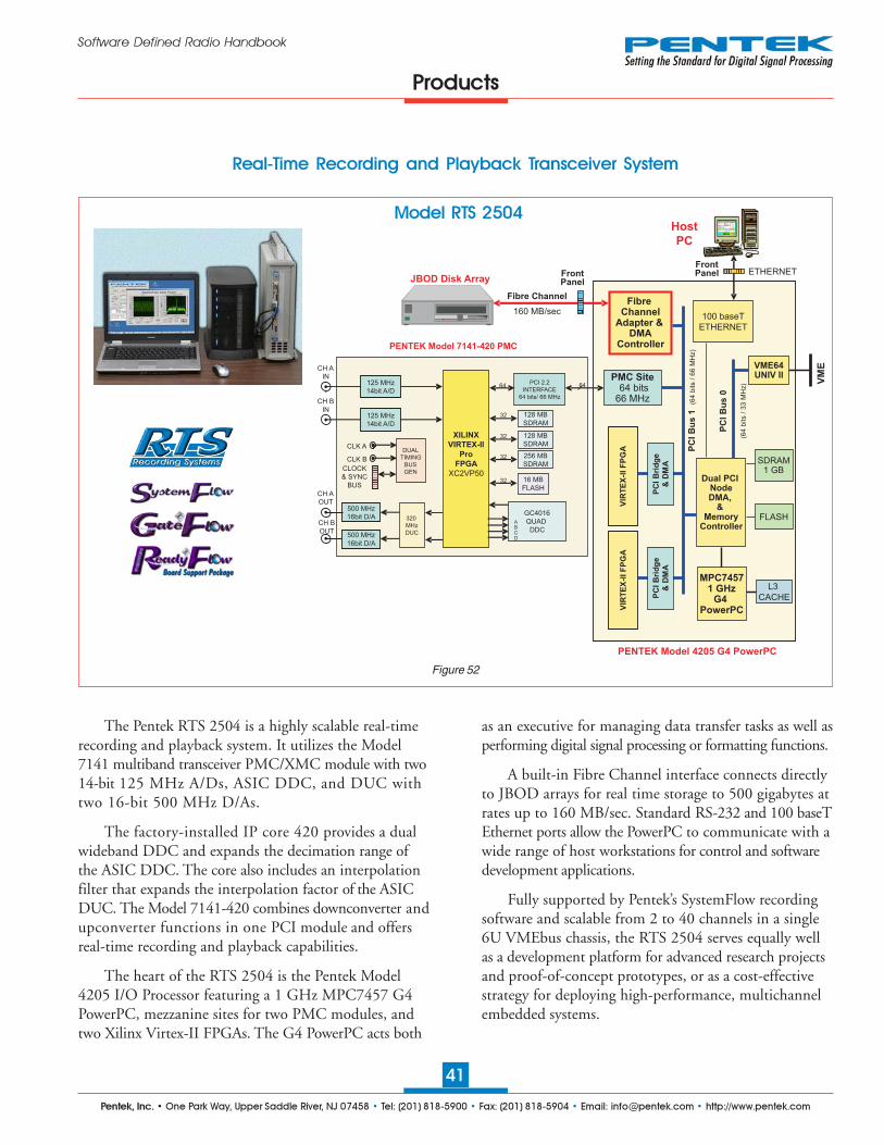
Pentek, Inc. • One Park Way, Upper Saddle River, NJ 07458 • Tel: (201) 818-5900 • Fax: (201) 818-5904 • Email: [email protected] • http://www.pentek.com
41
Software Defined Radio Handbook
Host
PC
Dual PCINodeDMA,
&Memory
Controller
FibreChannel
Adapter &DMA
Controller
VME64UNIV II
SDRAM1 GB
PC
IB
us
1(6
4bits
/66
MH
z)
PENTEK Model 4205 G4 PowerPC
100 baseT
ETHERNET
L3
CACHE
MPC74571 GHz
G4PowerPC
FLASH
VM
E
PC
IB
us
0
(64
bits
/33
MH
z)
PC
IB
rid
ge
&D
MA
VIR
TE
X-I
IF
PG
A
ETHERNETFrontPanel
PC
IB
rid
ge
&D
MA
VIR
TE
X-I
IF
PG
A
FrontPanel
Fibre Channel
160 MB/sec
PENTEK Model 7141-420 PMC
XILINX
VIRTEX-II
Pro
FPGA
XC2VP50
PCI 2.2
INTERFACE
64 bits/ 66 MHz
64 64
16 MB
FLASH32
256 MB
SDRAM
128 MB
SDRAM
128 MB
SDRAM
GC4016
QUAD
DDC
ABCD
DUAL
TIMING
BUS
GEN
CLK A
CLOCK
& SYNC
BUS
CLK B
320
MHz
DUC
CH A
OUT
CH B
OUT
500 MHz
16bit D/A
500 MHz
16bit D/A
125 MHz
14bit A/D
CH A
IN
125 MHz
14bit A/D
CH B
IN
32
32
32
PMC Site64 bits
66 MHz
JBOD Disk Array
Products
Real-Time Recording and Playback Transceiver System
The Pentek RTS 2504 is a highly scalable real-timerecording and playback system. It utilizes the Model7141 multiband transceiver PMC/XMC module with two14-bit 125 MHz A/Ds, ASIC DDC, and DUC withtwo 16-bit 500 MHz D/As.
The factory-installed IP core 420 provides a dualwideband DDC and expands the decimation range ofthe ASIC DDC. The core also includes an interpolationfilter that expands the interpolation factor of the ASICDUC. The Model 7141-420 combines downconverter andupconverter functions in one PCI module and offersreal-time recording and playback capabilities.
The heart of the RTS 2504 is the Pentek Model4205 I/O Processor featuring a 1 GHz MPC7457 G4PowerPC, mezzanine sites for two PMC modules, andtwo Xilinx Virtex-II FPGAs. The G4 PowerPC acts both
as an executive for managing data transfer tasks as well asperforming digital signal processing or formatting functions.
A built-in Fibre Channel interface connects directlyto JBOD arrays for real time storage to 500 gigabytes atrates up to 160 MB/sec. Standard RS-232 and 100 baseTEthernet ports allow the PowerPC to communicate with awide range of host workstations for control and softwaredevelopment applications.
Fully supported by Pentek’s SystemFlow recordingsoftware and scalable from 2 to 40 channels in a single6U VMEbus chassis, the RTS 2504 serves equally wellas a development platform for advanced research projectsand proof-of-concept prototypes, or as a cost-effectivestrategy for deploying high-performance, multichannelembedded systems.
Model RTS 2504
Figure 52

Pentek, Inc. • One Park Way, Upper Saddle River, NJ 07458 • Tel: (201) 818-5900 • Fax: (201) 818-5904 • Email: [email protected] • http://www.pentek.com
42
Software Defined Radio Handbook
Products
Rack-mount Real-Time Recording and Playback Transceiver Instrument
Model RTS 2701
Figure 53
The Pentek RTS 2701 is a highly scalable recordingand playback system in an industrial rack-mount PC serverchassis. Built on the Windows XP professional workstation,it utilizes the Model 7641-420 multiband transceiverPCI module with two 14-bit 125 MHz A/Ds, ASICDDC, and DUC with two 16-bit 500 MHz D/As.
The factory-installed IP core 420 provides a dualwideband DDC and expands the decimation range ofthe ASIC DDC. The core also includes an interpolationfilter that expands the interpolation factor of the ASICDUC. The Model 7641-420 combines downconverter andupconverter functions in one PCI module and offersrecording and playback capabilities.
Included with this instrument is Pentek’s System-Flow recording software.The RTS 2701 uses a nativeNTFS record/playback file format for easy access by user
applications for analysis, signal processing, and waveformgeneration. File headers include recording parametersettings and time stamping so that the signal viewercorrectly formats and annotates the displayed signals.
A high-performance PCI Express SATA RAIDcontroller connects to multiple SATA hard drives tosupport storage to 5 terabytes and real-time recordingrates to 480 MB/sec.
Multiple RAID levels, including 0, 1, 5, 6, 10 and50, provide a choice for the required level of redundancy.The Pentek RTS 2701 serves equally well as a develop-ment platform for advanced research projects and proof-of-concept prototypes, or as a cost-effective strategy fordeploying high-performance, multichannel embeddedsystems.
DDR
SDRAM
RAID
CONTROLLER
INTEL
PROCESSOR
RAID ARRAY
DATA
DRIVES
DATA
DRIVES
DATA
DRIVES
DATA
DRIVES
SYSTEMDRIVE
SAMPLE
CLOCK
AND
SYNC
GENERATOR
125 MHz
14-BIT A/DCH 2 IN
500 MHz
16-BIT D/ACH 1 OUT
CLK A IN
CLK B IN
TTL GATE/
TRIG IN
CLOCK
SYNC
BUS
125 MHz
14-BIT A/DCH 1 IN
DIGITAL
DOWN
CONVERTER
DIGITAL
DOWN
CONVERTER
DIGITAL
UP
CONVERTER
XTAL
OSC
A
XTAL
OSC
B
GIGABIT ENET
USB 2.0
PS/2 KEYBOARD
PS/2 MOUSE
AUX VIDEO OUT
PENTEK RTS 2701 RECORDER
MODEL 7641-420TRANSCEIVER
-
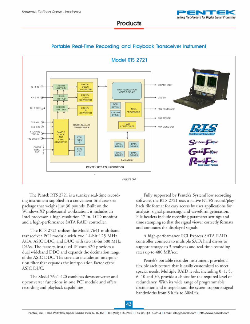
Pentek, Inc. • One Park Way, Upper Saddle River, NJ 07458 • Tel: (201) 818-5900 • Fax: (201) 818-5904 • Email: [email protected] • http://www.pentek.com
43
Software Defined Radio Handbook
Products
Portable Real-Time Recording and Playback Transceiver Instrument
Model RTS 2721
Figure 54
The Pentek RTS 2721 is a turnkey real-time record-ing instrument supplied in a convenient briefcase-sizepackage that weighs just 30 pounds. Built on theWindows XP professional workstation, it includes anIntel processor, a high-resolution 17 in. LCD monitorand a high-performance SATA RAID controller.
The RTS 2721 utilizes the Model 7641 multibandtransceiver PCI module with two 14-bit 125 MHzA/Ds, ASIC DDC, and DUC with two 16-bit 500 MHzD/As. The factory-installed IP core 420 provides adual wideband DDC and expands the decimation rangeof the ASIC DDC. The core also includes an interpola-tion filter that expands the interpolation factor of theASIC DUC.
The Model 7641-420 combines downconverter andupconverter functions in one PCI module and offersrecording and playback capabilities.
Fully supported by Pentek’s SystemFlow recordingsoftware, the RTS 2721 uses a native NTFS record/play-back file format for easy access by user applications foranalysis, signal processing, and waveform generation.File headers include recording parameter settings andtime stamping so that the signal viewer correctly formatsand annotates the displayed signals.
A high-performance PCI Express SATA RAIDcontroller connects to multiple SATA hard drives tosupport storage to 3 terabytes and real-time recordingrates up to 480 MB/sec.
Pentek’s portable recorder instrument provides aflexible architecture that is easily customized to meetspecial needs. Multiple RAID levels, including 0, 1, 5,6, 10 and 50, provide a choice for the required level ofredundancy. With its wide range of programmabledecimation and interpolation, the system supports signalbandwidths from 8 kHz to 60MHz.
DDR
SDRAM
RAID
CONTROLLER
INTEL
PROCESSOR
RAID ARRAY
DATA
DRIVES
DATA
DRIVES
DATA
DRIVES
DATA
DRIVES
SYSTEMDRIVE
SAMPLE
CLOCK
AND
SYNC
GENERATOR
125 MHz
14-BIT A/DCH 2 IN
500 MHz
16-BIT D/ACH 1 OUT
CLK A IN
CLK B IN
TTL GATE/
TRIG IN
CLOCK
SYNC
BUS
TTL SYNC IN
125 MHz
14-BIT A/DCH 1 IN
HIGH RESOLUTION
VIDEO DISPLAY
DIGITAL
DOWN
CONVERTER
DIGITAL
DOWN
CONVERTER
DIGITAL
UP
CONVERTER
XTAL
OSC
A
XTAL
OSC
B
GIGABIT ENET
USB 2.0
PS/2 KEYBOARD
PS/2 MOUSE
AUX VIDEO OUT
PENTEK RTS 2721 RECORDER
MODEL 7641-420TRANSCEIVER
-
Pentek, Inc. • One Park Way, Upper Saddle River, NJ 07458 • Tel: (201) 818-5900 • Fax: (201) 818-5904 • Email: [email protected] • http://www.pentek.com
44
Software Defined Radio Handbook
Applications
Applications of Software Defined Radio
Software Radio can be used in many different systems:
Tracking receivers can be highly automated becausesoftware radio allows DSPs to perform the signalidentification and analysis functions as well as theadaptable tuning functions.
Signal intelligence applications and radar benefitfrom the tight coupling of the A/D, DDC, DUC, andDSP functions to process wideband signals.
Cellular phone applications are one of the strongesthigh-volume applications because of the high density of
tightly-packed frequency division multiplexed voicechannels.
Direction finding and beamforming are idealapplications for digital receivers because of their excel-lent channel-to-channel phase and gain matching andconsistent delay characteristics.
As a general capability, any system requiring atunable bandpass filter should be considered a candidatefor using DDCs. Take a look at the following applicationexamples to give you some more details.
● Tracking Receiver System
● Software Radio Transceiver System
● 512-Channel SDR System in a single VMEbus Slot
● Radar Signal Processing System
● 8-Channel Beamforming System
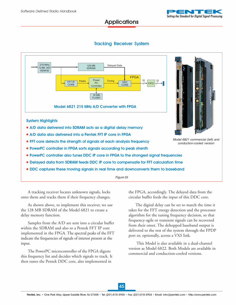
Pentek, Inc. • One Park Way, Upper Saddle River, NJ 07458 • Tel: (201) 818-5900 • Fax: (201) 818-5904 • Email: [email protected] • http://www.pentek.com
45
Software Defined Radio Handbook
Tracking Receiver System
A tracking receiver locates unknown signals, locksonto them and tracks them if their frequency changes.
As shown above, to implement this receiver, we usethe 128 MB SDRAM of the Model 6821 to create adelay memory function.
Samples from the A/D are sent into a circular bufferwithin the SDRAM and also to a Pentek FFT IP coreimplemented in the FPGA. The spectral peaks of the FFTindicate the frequencies of signals of interest present at theinput.
The PowerPC microcontroller of the FPGA digeststhis frequency list and decides which signals to track. Itthen tunes the Pentek DDC core, also implemented in
the FPGA, accordingly. The delayed data from thecircular buffer feeds the input of this DDC core.
The digital delay can be set to match the time ittakes for the FFT energy detection and the processoralgorithm for the tuning frequency decision, so thatfrequency-agile or transient signals can be recoveredfrom their onset. The dehopped baseband output isdelivered to the rest of the system through the FPDPport or, optionally, across a VXS link.
This Model is also available in a dual-channelversion as Model 6822. Both Models are available incommercial and conduction-cooled versions.
Figure 55
Applications
System Highlights
● ● ● ● ● A/D data delivered into SDRAM acts as a digital delay memory
● ● ● ● ● A/D data also delivered into a Pentek FFT IP core in FPGA
● ● ● ● ● FFT core detects the strength of signals at each analysis frequency
● ● ● ● ● PowerPC controller in FPGA sorts signals according to peak strenth
● ● ● ● ● PowerPC controller also tunes DDC IP core in FPGA to the strongest signal frequencies
● ● ● ● ● Delayed data from SDRAM feeds DDC IP core to compensate for FFT calculation time
● ● ● ● ● DDC captures these moving signals in real time and downconverts them to baseband
Model 6821 215 MHz A/D Converter with FPGA
Model 6821 commercial (left) andconduction-cooled version
32 32FIFO
Delayed Data
16 MBFLASH
Power
PC
Controller
DDCCORE
Tuning
128 MBSDRAM
215 MHz
12-Bit A/D
AD9430
FFT IPCORE
Peaks
FPGA

Pentek, Inc. • One Park Way, Upper Saddle River, NJ 07458 • Tel: (201) 818-5900 • Fax: (201) 818-5904 • Email: [email protected] • http://www.pentek.com
46
Software Defined Radio Handbook
4-Channel Software Radio Transceiver System
Figure 56
This system accepts four analog inputs frombaseband or IF signals with bandwidths up to 50 MHzand IF center frequencies up to 150 MHz. A total ofeight DDC channels are independently tunable acrossthe input band and can deliver downconverted outputsignal bandwidths from audio up to 2.5 MHz.
Four analog outputs can deliver baseband or IFsignals with bandwidths up to about 50 MHz and IFcenter frequencies up to 100 MHz. The system supportsfour independent D/A channels or two upconvertedchannels with real or quadrature outputs.
Signal processing resources include the FreescaleMPC8641 AltiVec processor and an FX60 or FX100Virtex-4 FPGA on the Model 4207 I/O processor, plusa Virtex-II VP-50 FPGA on each PMC module.
Using these on-board processing resources thispowerful system can process analog input data locallyand deliver it to the analog outputs. It can also be usedas a pre- and post-processing I/O front end for sendingand receiving data to other system boards connectedover the VMEbus or through switched fabric links usingthe VXS interface.
Ruggedized and conduction-cooled versions of theboards used in this system are available.
Applications
P14
PENTEK Model 7141
256 MB
SDRAM
128 MBSDRAM
128 MBSDRAM
CH A IN
32
32
32
CH B IN
64
320 MHzDUC
PCI INTERFACE
PCI
PENTEK Model 7141
256 MB
SDRAM
128 MBSDRAM
128 MBSDRAM
CH A IN
32
32
32
CH B IN
64
320 MHz
DUC
16 MB
FLASH
32
4
4QUADDDC
GC4106
125 MHz14bit A/D
125 MHz
14bit A/D
PCI INTERFACE
PCI
XILINX
VIRTEX-II
PRO
VP50
16 MB
FLASH
32
4
4QUAD
DDCGC4106
CLK A
CLOCK& SYNC
BUS
CLK BDUAL TIMINGBUS GEN
125 MHz14bit A/D
125 MHz14bit A/D
PCI-X Bus 0(64 Bits, 100 MHz)
PCI-X Bus 1(64 Bits, 100 MHz)
VME64x
2eSST
VME64x
ZeroLatencyCrossbarSwitch
Dual 4 GbitFibre Channel
Dual 4 Gb FibreChannel Controller
MPC8641Single/Dual Core
32 MBFLASHFLASH256 MB
32 MBFLASHFLASH128 MB
DDR2 SDRAM1 GB
Front PanelOptical
Interface
2x
Dual4x
Dual4x
8xSRIO4x
Dual4x
2x
XMC /
PMC Site
XMC /
PMC Site
XMC /
PMC Site
XMC /
PMC Site
PCIe toPCI-X Bridge
PCIe toPCI-X Bridge
DDR2SDRAM
1 GB
VXS VITA 41
Dual4x
2xGigabit
ENET-x
Virtex-4 FPGA
XC4VFX60 / FX100
To VME P2
PENTEK Model 4207
Dual1000BT
Enet
QuadRS-
232C
CLOCK& SYNC
BUS
CLK A
CLK B DUAL TIMINGBUS GEN
XILINX
VIRTEX-II
PRO
VP50
CH AOUT
500 MHz
16bit D/A
CH BOUT
CH AOUT
500 MHz
16bit D/A
CH BOUT

Pentek, Inc. • One Park Way, Upper Saddle River, NJ 07458 • Tel: (201) 818-5900 • Fax: (201) 818-5904 • Email: [email protected] • http://www.pentek.com
47
Software Defined Radio Handbook
512-Channel Software Radio Recording System in a Single VMEbus Slot
Figure 57
Each Model 7141 PMC features the Xilinx Virtex-IIPro VP50 with a Pentek 256-Channel Digital Down-converter (DDC) IP Core 430. Each channel providesindependent tuning frequency with a global decimationfrom 1024 to 9984. Either one of the two 14-bit A/Dconverters operating at 125 MHz sample rate can feedthis core producing a range of output bandwidths from10 kHz to 100 kHz.
A dual 4-Gbit Fibre Channel copper interfaceallows wideband A/D data or DDC outputs from all512 channels to be recorded in real time to a RAID orJBOD disk array at aggregate rates up to 640 MB/sec.
Pentek’s SystemFlow® software presents an intuitivegraphical user interface (GUI) to set up the DDCchannels and recording mode. The GUI executes on aWindows host PC connected to the 4207 via Ethernet.
A SystemFlow signal viewer on the PC allowspreviewing of data prior to recording and viewing ofrecorded data files in both time and frequency domains.Files can be moved between the Fibre Channel disk andthe PC over Ethernet.
This system is ideal for downconverting and capturingreal time signal data from a very large number ofchannels in an extremely compact, low cost system.
Applications
P14
PENTEK Model 7141-430
256 MB
SDRAM
128 MB
SDRAM
128 MB
SDRAM
CH A IN
32
32
32
CH B IN
64
320 MHz
DUC
PCI INTERFACE
PCI
PENTEK Model 7141-430
256 MB
SDRAM
128 MB
SDRAM
128 MB
SDRAM
CH A IN
32
32
32
CH B IN
64
320 MHz
DUC
16 MB
FLASH
32
4
4QUAD
DDC
GC4106
125 MHz
14bit A/D
125 MHz
14bit A/D
PCI INTERFACE
PCI
XILINX
VIRTEX-II
PRO
VP50
IP CORE
430
256-CHAN
DIGITAL
DOWN
CONVERTER
16 MB
FLASH
32
4
4QUAD
DDC
GC4106
CLK A
CLOCK
& SYNC
BUS
CLK BDUAL TIMING
BUS GEN
125 MHz
14bit A/D
125 MHz
14bit A/D
PCI-X Bus 0
(64 Bits, 100 MHz)
PCI-X Bus 1
(64 Bits, 100 MHz)
VME64x
2eSST
VME64x
ZeroLatency
CrossbarSwitch
Dual 4 Gbit
Fibre Channel
Dual 4 Gb FibreChannel Controller
MPC8641Single/Dual Core
32 MBFLASHFLASH256 MB
32 MBFLASHFLASH128 MB
DDR2 SDRAM1 GB
Front PanelOptical
Interface
2x
Dual4x
Dual4x
8x
SRIO8x
Dual4x
2x
XMC /
PMC Site
XMC /
PMC Site
XMC /
PMC Site
XMC /
PMC Site
PCIe toPCI-X Bridge
PCIe toPCI-X Bridge
DDR2SDRAM
1 GB
VXS VITA 41
Dual4x2xGigabit
ENET-x
Virtex-4 FPGA
XC4VFX60 / FX100
To VME P2
PENTEK Model 4207
Dual1000BT
Enet
QuadRS-
232C
CLOCK
& SYNC
BUS
CLK A
CLK B DUAL TIMING
BUS GEN
XILINX
VIRTEX-II
PRO
VP50
CH A
OUT
500 MHz
16bit D/A
CH B
OUT
CH A
OUT
500 MHz
16bit D/A
CH B
OUT
JBOD Disk Array
2x
IP CORE
430
256-CHAN
DIGITAL
DOWN
CONVERTER
IP CORE
430
256-CHAN
DIGITAL
DOWN
CONVERTER

Pentek, Inc. • One Park Way, Upper Saddle River, NJ 07458 • Tel: (201) 818-5900 • Fax: (201) 818-5904 • Email: [email protected] • http://www.pentek.com
48
Software Defined Radio Handbook
Radar Signal Processing System
Applications
Radar is well served by high-speed A/D convertersand wideband digital downconverters. The channelizedsystem shown above, takes advantage of a Model7142-428 multichannel transceiver with an installedFPGA core that includes four wideband DDCs and aninterpolation filter.
Operating at sampling rates up to 125 MHz, theA/D converters can digitize baseband signals withbandwidths up to 50 MHz. After frequency translationand filtering, the DDCs deliver complex (I & Q) datato the Model 4207 processor board. Here, data may beprocessed by custom user-defined algorithms before it issent across the VXS interface for recording and off-lineprocessing.
The optional GateFlow FPGA Design Kit can beused to install custom algorithms in the Model 4207
FPGA. Factory-installed IP cores such as pulse compres-sion and FFT are available and can be factory installedin this FPGA.
The upconverter with the interpolation filter can beused to generate arbitrary radar pulse waveforms thatcan be used to calibrate the system. The D/A output canalso be used for countermeasures, such as jamming orspoofing.
Jamming blasts energy that disables radars, andspoofing deceives radars by making it seem that thetarget is a different shape, speed, direction or distance byusing DSP techniques. This is especially useful for a jetor UAV to prevent it from getting shot down.
Note that one more PMC/XMC site is available forinstallation of an additional module.
P14
PENTEK Model 7142-428
256 MB
SDRAM
256 MB
SDRAM
256 MB
SDRAM
CH A IN
32
32
32
CH B IN
64
320 MHz
DUC
16 MB
FLASH
32
125 MHz
14bit A/D
125 MHz
14bit A/D
PCI-X Bus 0
(64 Bits, 100 MHz)
PCI-X Bus 1
(64 Bits, 100 MHz)
VME64x
2eSST
VME64x
ZeroLatency
CrossbarSwitch
Dual 4 Gbit
Fibre Channel
Dual 4 Gb FibreChannel Controller
MPC8641Single/Dual Core
32 MBFLASHFLASH256 MB
32 MBFLASHFLASH128 MB
DDR2 SDRAM1 GB
Front PanelOptical
Interface
2x
Dual4x
Dual4x
8x
SRIO4x
Dual4x
2x
XMC /
PMC SiteXMC /
PMC Site
XMC /
PMC Site
XMC /
PMC Site
PCIe toPCI-X Bridge
PCIe toPCI-X Bridge
DDR2SDRAM
1 GB
VXS VITA 41
Dual4x2xGigabit
ENET-x
Virtex-4 FPGA
XC4VFX60 / FX100
To VME P2
PENTEK Model 4207
Dual1000BT
Enet
QuadRS-
232C
CLOCK
& SYNC
BUS
XILINX
VIRTEX-4
FPGA
With
4-chan.
DDC &
Interpol.
Filter
CH A
OUT500 MHz
16bit D/A
CLK ADUAL TIMING
BUS GEN
CH C IN
CH D IN
125 MHz
14bit A/D
125 MHz
14bit A/D
VIRTEX-4 FPGA
FX60 or FX100
PCI XMCI/O
Dual4x
96
Figure 58
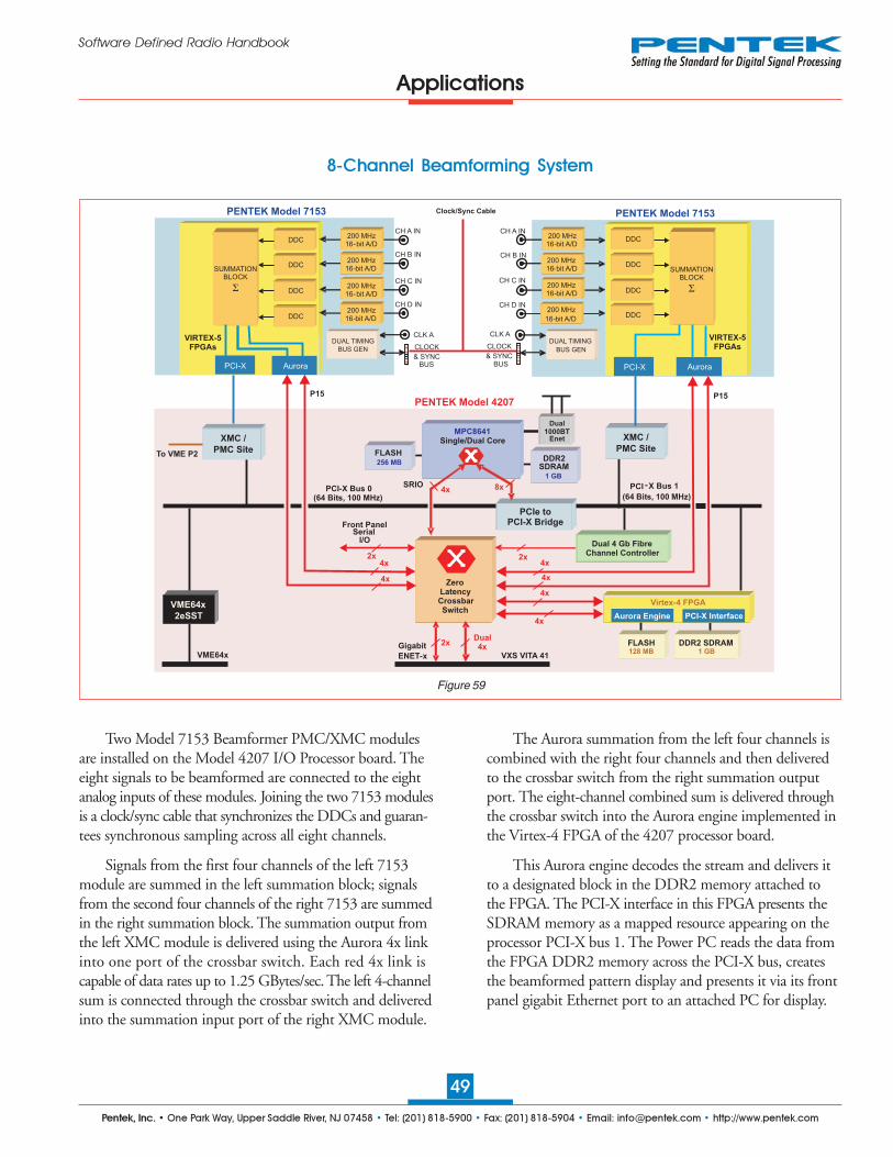
Pentek, Inc. • One Park Way, Upper Saddle River, NJ 07458 • Tel: (201) 818-5900 • Fax: (201) 818-5904 • Email: [email protected] • http://www.pentek.com
49
Software Defined Radio Handbook
Applications
Figure 59
8-Channel Beamforming System
P15 P15
PENTEK Model 7153
CH A IN
CH B IN
PENTEK Model 7153
CH A IN
CH B IN
200 MHz16-bit A/D
200 MHz16-bit A/D
CLOCK
Clock/Sync Cable
& SYNCBUS
CLK ADUAL TIMING
BUS GEN
200 MHzDDC
DDC
DDC
DDC
16-bit A/D
200 MHz16-bit A/D
PCI-X Bus 0(64 Bits, 100 MHz)
PCI -X Bus 1
(64 Bits, 100 MHz)
VME64x
2eSST
VME64x
ZeroLatencyCrossbarSwitch
Dual 4 GbitFibre Channel
Dual 4 Gb FibreChannel Controller
MPC8641Single/Dual Core
32 MBFLASHFLASH256 MB
32 MBFLASHFLASH128 MB
DDR2 SDRAM1 GB
Front PanelSerial
I/O
2x
4x
4x
4x
4x
8xSRIO4x
4x
4x
2x
XMC /
PMC Site
XMC /
PMC Site
XMC /
PMC Site
XMC /
PMC Site
PCIe toPCI-X Bridge
PCIe toPCI-X Bridge
DDR2SDRAM
1 GB
VXS VITA 41
Dual4x
2xGigabit
ENET-x
Virtex-4 FPGA
To VME P2
PENTEK Model 4207
CLOCK
& SYNCBUS
CH C IN
CH D IN
200 MHz16-bit A/D
200 MHz16-bit A/D
VIRTEX-5FPGAs
PCI-X Aurora
CLK A
CH C IN
CH D IN
200 MHz16-bit A/D
200 MHz
16-bit A/D
SUMMATIONBLOCK
�
DDC
DDC
DDC
DDC
PCI-X Aurora
SUMMATIONBLOCK
�
DUAL TIMING
BUS GEN
VIRTEX-5FPGAs
Aurora Engine PCI-X Interface
Dual1000BT
Enet
Two Model 7153 Beamformer PMC/XMC modulesare installed on the Model 4207 I/O Processor board. Theeight signals to be beamformed are connected to the eightanalog inputs of these modules. Joining the two 7153 modulesis a clock/sync cable that synchronizes the DDCs and guaran-tees synchronous sampling across all eight channels.
Signals from the first four channels of the left 7153module are summed in the left summation block; signalsfrom the second four channels of the right 7153 are summedin the right summation block. The summation output fromthe left XMC module is delivered using the Aurora 4x linkinto one port of the crossbar switch. Each red 4x link iscapable of data rates up to 1.25 GBytes/sec. The left 4-channelsum is connected through the crossbar switch and deliveredinto the summation input port of the right XMC module.
The Aurora summation from the left four channels iscombined with the right four channels and then deliveredto the crossbar switch from the right summation outputport. The eight-channel combined sum is delivered throughthe crossbar switch into the Aurora engine implemented inthe Virtex-4 FPGA of the 4207 processor board.
This Aurora engine decodes the stream and delivers itto a designated block in the DDR2 memory attached tothe FPGA. The PCI-X interface in this FPGA presents theSDRAM memory as a mapped resource appearing on theprocessor PCI-X bus 1. The Power PC reads the data fromthe FPGA DDR2 memory across the PCI-X bus, createsthe beamformed pattern display and presents it via its frontpanel gigabit Ethernet port to an attached PC for display.

Pentek, Inc. • One Park Way, Upper Saddle River, NJ 07458 • Tel: (201) 818-5900 • Fax: (201) 818-5904 • Email: [email protected] • http://www.pentek.com
50
Software Defined Radio Handbook
• Reduction of DSP processing demands
• Very fast tuning
• Fast bandwidth selection
• Zero frequency drift and error
• Precise, stable filter characteristics
• Excellent dynamic range
SDR Benefits
Benefits of Software Defined Radio:
To summarize, we restate the major benefits:
SDRs can dramatically reduce the DSP requirements forsystems which need to process signals contained within a certainfrequency band of a wideband signal.
The fast tuning of the digital local oscillator and theeasy bandwidth selection in the decimating digital filterand interpolation filter make the SDR easy to control.
Since the entire circuitry uses digital signal process-ing, the characteristics are precise, predictable, and willnot drift with time, temperature or aging. This alsomeans excellent channel-to-channel matching and no needfor calibration, alignment or maintenance.
With the addition of FPGA technology, dramaticincreases in system density have been coupled with asignificantly lower cost per channel. Furthermore,FPGA technology allows one to incorporate customalgorithms right at the front end of these systems.
As we have seen, there are inherently many benefitsand advantages to when using SDR. We hope that thisintroduction has been informative. We stand ready todiscuss your requirements and help you configure acomplete SDR system.
For all the latest information about Pentek SDRs,DSP boards and data acquisition products, be sure tovisit Pentek’s comprehensive website regularly.
Pentek offers a comprehensive array of VMEbusDSP boards featuring the AltiVec G4 PowerPC fromFreescale and the TMS320C6000 family of processorproducts from Texas Instruments.
On-board processor densities range from one toeight DSPs with many different memory and interfaceoptions available.
The Models 4205 and 4207 I/O processor boardsfeature the latest G4 PowerPCs, accept PMC mezzaninesand include built-in Fibre Channel interfaces.
The Models 4294 and 4295 processor boards featurefour MPC74xx G4 PowerPC processors utilizing theAltiVec vector processor capable of delivering severalGFLOPS of processing power.
The Models 4292 and 4293 processor boards featurethe Texas Instruments latest TMS320C6000 family offixed-point DSPs that represent a 10-fold increase inprocessing power over previous designs.
Once again, the ability of the system designer tofreely choose the most appropriate DSP processor foreach software radio application, facilitates systemrequirement changes and performance upgrades.
Full software development tools are available for work-stations running Windows and Linux with many differentdevelopment system configurations available.
DSP Boards for VMEbus
Summary
Figure 60
• Freescale Altivec G4PowerPC
• Texas InstrumentsC6000 DSPs
• Single, Dual, Quad andOctal Processor versions
• PMC, PMC/XMC, PCIand cPCI I/O peripherals
• VME/VXS platforms
Figure 61
Pentek, Inc. • One Park Way, Upper Saddle River, NJ 07458 • Tel: (201) 818-5900 • Fax: (201) 818-5904 • Email: [email protected] • http://www.pentek.com
51
Software Defined Radio Handbook
Links
More links on the next page ➤
The following links provide you with additional information about the Pentek productspresented in this handbook: just click on the Model number. Links are also provided to otherhandbooks or brochures that may be of interest in your software radio development projects.
Model Description Page
7131 Multiband Receiver - PMC 19
7231 Multiband Receiver - 6U cPCI 19
7331 Multiband Receiver - 3U cPCI 19
7631A Multiband Receiver - PCI 19
7140 Multiband Transceiver with Virtex-II Pro FPGA - PMC/XMC 20
7240 Multiband Transceiver with Virtex-II Pro FPGA - 6U cPCI 20
7340 Multiband Transceiver with Virtex-II Pro FPGA - 3U cPCI 20
7640 Multiband Transceiver with Virtex-II Pro FPGA - PCI 20
7140-420 Transceiver w. Dual Wideband DDC and Interpolation Filter - PMC/XMC 21
7240-420 Transceiver w. Dual Wideband DDC and Interpolation - 6U cPCI 21
7340-420 Transceiver w. Dual Wideband DDC and Interpolation - 3U cPCI 21
7640-420 Transceiver w. Dual Wideband DDC and Interpolation - PCI 21
7140-430 Transceiver w. 256-Channel Narrowband DDC - PMC/XMC 22
7240-430 Transceiver w. 256-Channel Narrowband DDC - 6U cPCI 22
7340-430 Transceiver w. 256-Channel Narrowband DDC - 3U cPCI 22
7640-430 Transceiver w. 256-Channel Narrowband DDC - PCI 22
7141 Multiband Transceiver with Virtex-II Pro FPGA - PMC/XMC 23
7241 Multiband Transceiver with Virtex-II Pro FPGA - 6U cPCI 23
7341 Multiband Transceiver with Virtex-II Pro FPGA - 3U cPCI 23
7641 Multiband Transceiver with Virtex-II Pro FPGA - PCI 23
7741 Multiband Transceiver with Virtex-II Pro FPGA - Full-length PCIe 23
7841 Multiband Transceiver with Virtex-II Pro FPGA - Half-length PCIe 23
7141-420 Transceiver w. Dual Wideband DDC and Interpolation Filter - PMC/XMC 24
7241-420 Transceiver w. Dual Wideband DDC and Interpolation Filter - 6U cPCI 24
7341-420 Transceiver w. Dual Wideband DDC and Interpolation Filter - 3U cPCI 24
7641-420 Transceiver w. Dual Wideband DDC and Interpolation Filter - PCI 24
7741-420 Transceiver w. Dual Wideband DDC and Interpolation Filter - Full-length PCIe 24
7841-420 Transceiver w. Dual Wideband DDC and Interpolation Filter - Half-length PCIe 24
7141-430 Transceiver w. 256-Channel Narrowband DDC - PMC/XMC 25
7241-430 Transceiver w. 256-Channel Narrowband DDC - 6U cPCI 25
7341-430 Transceiver w. 256-Channel Narrowband DDC - 3U cPCI 25
7641-430 Transceiver w. 256-Channel Narrowband DDC - PCI 25
7741-430 Transceiver w. 256-Channel Narrowband DDC - Full-length PCIe 25
7841-430 Transceiver w. 256-Channel Narrowband DDC - Half-length PCIe 25
7141-703 Conduction-cooled Multiband Transceiver - PMC/XMC 25
7142 Multichannel Transceiver with Virtex-4 FPGAs - PMC/XMC 26
7242 Multichannel Transceiver with Virtex-4 FPGAs - 6U cPCI 26
7342 Multichannel Transceiver with Virtex-4 FPGAs - 3U cPCI 26
7642 Multichannel Transceiver with Virtex-4 FPGAs - PCI 26
7742 Multichannel Transceiver with Virtex-4 FPGAs - Full-length PCIe 26
7842 Multichannel Transceiver with Virtex-4 FPGAs - Half-length PCIe 26
Pentek, Inc. • One Park Way, Upper Saddle River, NJ 07458 • Tel: (201) 818-5900 • Fax: (201) 818-5904 • Email: [email protected] • http://www.pentek.com
52
Software Defined Radio Handbook
Links
Model Description Page
7142-428 Multichannel Transceiver w. Four Multiband DDCs and Interpolation Filter - PMC/XMC 27
7242-428 Multichannel Transceiver w. Four Multiband DDCs and Interpolation Filter- 6U cPCI 27
7342-428 Multichannel Transceiver w. Four Multiband DDCs and Interpolation Filter- 3U cPCI 27
7642-428 Multichannel Transceiver w. Four Multiband DDCs and Interpolation Filter- PCI 27
7742-428 Multichannel Transceiver w. Four Multiband DDCs and Interpolation Filter- Full-length PCIe 27
7842-428 Multichannel Transceiver w. Four Multiband DDCs and Interpolation Filter- Half-length PCIe 27
7151 256-Channel DDC with Quad 200 MHz, 16-bit A/D - PMC 28
7251 256-Channel DDC with Quad 200 MHz, 16-bit A/D - 6U cPCI 28
7351 256-Channel DDC with Quad 200 MHz, 16-bit A/D - 3U cPCI 28
7651 256-Channel DDC with Quad 200 MHz, 16-bit A/D - PCI 28
7751 256-Channel DDC with Quad 200 MHz, 16-bit A/D - Full-length PCIe 28
7851 256-Channel DDC with Quad 200 MHz, 16-bit A/D - Half-length PCIe 28
7152 32-Channel DDC with Quad 200 MHz, 16-bit A/D - PMC 29
7252 32-Channel DDC with Quad 200 MHz, 16-bit A/D - 6U cPCI 29
7352 32-Channel DDC with Quad 200 MHz, 16-bit A/D - 3U cPCI 29
7652 32-Channel DDC with Quad 200 MHz, 16-bit A/D - PCI 29
7752 32-Channel DDC with Quad 200 MHz, 16-bit A/D - Full-length PCIe 29
7852 32-Channel DDC with Quad 200 MHz, 16-bit A/D - Half-length PCIe 29
7153 4-Channel DDC with Quad 200 MHz, 16-bit A/D - PMC/XMC 30
7253 4-Channel DDC with Quad 200 MHz, 16-bit A/D - 6U cPCI 30
7353 4-Channel DDC with Quad 200 MHz, 16-bit A/D - 3U cPCI 30
7653 4-Channel DDC with Quad 200 MHz, 16-bit A/D - PCI 30
7753 4-Channel DDC with Quad 200 MHz, 16-bit A/D - Full-length PCIe 30
7853 4-Channel DDC with Quad 200 MHz, 16-bit A/D - Half-length PCIe 30
7156 Dual SDR Transceiver, 400 MHz A/D, 800 MHz D/A, Virtex-5 FPGAs - PMC/XMC 31
7256 Dual SDR Transceiver, 400 MHz A/D, 800 MHz D/A, Virtex-5 FPGAs - 6U cPCI 31
7356 Dual SDR Transceiver, 400 MHz A/D, 800 MHz D/A, Virtex-5 FPGAs - 3U cPCI 31
7656 Dual SDR Transceiver, 400 MHz A/D, 800 MHz D/A, Virtex-5 FPGAs - PCI 31
7756 Dual SDR Transceiver, 400 MHz A/D, 800 MHz D/A, Virtex-5 FPGAs - Full-length PCIe 31
7856 Dual SDR Transceiver, 400 MHz A/D, 800 MHz D/A, Virtex-5 FPGAs - Half-length PCIe 31
7158 Dual SDR Transceiver, 500 MHz A/D, 800 MHz D/A, Virtex-5 FPGAs - PMC/XMC 32
7258 Dual SDR Transceiver, 500 MHz A/D, 800 MHz D/A, Virtex-5 FPGAs - 6U cPCI 32
7358 Dual SDR Transceiver, 500 MHz A/D, 800 MHz D/A, Virtex-5 FPGAs - 3U cPCI 32
7658 Dual SDR Transceiver, 500 MHz A/D, 800 MHz D/A, Virtex-5 FPGAs - PCI 32
7758 Dual SDR Transceiver, 500 MHz A/D, 800 MHz D/A, Virtex-5 FPGAs - Full-length PCIe 32
7858 Dual SDR Transceiver, 500 MHz A/D, 800 MHz D/A, Virtex-5 FPGAs - Half-length PCIe 32
71620 3-Channel 200 MHz A/D, DUC, 2-Channel 800 MHz D/A, Virtex-6 FPGA 33
More links on the next page ➤

Pentek, Inc. • One Park Way, Upper Saddle River, NJ 07458 • Tel: (201) 818-5900 • Fax: (201) 818-5904 • Email: [email protected] • http://www.pentek.com
53
Software Defined Radio Handbook
Model Description Page
Links
6821-422 215 MHz, 12-bit A/D with Wideband DDCs - VME/VXS 34
6822-422 Dual 215 MHz, 12-bit A/D with Wideband DDCs - VME/VXS 35
6826 Dual 2 GHz 10-bit A/D - VME/VXS 36
6890 2.2 GHz Clock, Sync and Gate Distribution Board - VME 37
6891 System Synchronizer and Distribution Board - VME 38
7190 Multifrequency Clock Synthesizer - PMC 39
7290 Multifrequency Clock Synthesizer - 6U cPCI 39
7390 Multifrequency Clock Synthesizer - 3U cPCI 39
7690 Multifrequency Clock Synthesizer - PCI 39
7790 Multifrequency Clock Synthesizer - Full-length PCIe 39
7890 Multifrequency Clock Synthesizer - Half-length PCIe 39
9190 Clock and Sync Generator for I/O Modules 40
RTS 2504 Real-Time Recording and Playback Transceiver System 41
4205 PowerPC I/O Processor - VME 41
RTS 2701 Rack-Mount Real-Time Recording and Playback Transceiver System 42
RTS 2721 Portable Real-Time Recording and Playback Transceiver Instrument 43
4207 PowerPC and FPGA I/O Processor - VME/VXS 46
Handbooks and Brochures
Click here Putting FPGAs to Work for Software Radio Hanbook
Click here Critical Techniques for High-Speed A/D Converters in Real-Time Systems Handbook
Click here High-Speed Switched Serial Fabrics Improve System Design Handbook
Click here Model 4207 PowerPC and FPGA I/O Processor Board Brochure