Soft-Switching in DC-DC Convertersaboutme.samexent.com/classes/spring09/ee5741/Soft... ·...
31
1 Soft-Switching in DC-DC Converters: Principles, Practical Topologies, Design Techniques, Latest Developments Raja Ayyanar Arizona State University Ned Mohan University of Minnesota Eric Persson International Rectifier © 2002, N. Mohan, R. Ayyanar, E. Persson APEC 2002 Some of the slides in this presentation are used for the course EE5741 Advanced Power Electronics given by Prof Robbins and Prof Mohan at the University of Minnesota
Transcript of Soft-Switching in DC-DC Convertersaboutme.samexent.com/classes/spring09/ee5741/Soft... ·...

1
Soft-Switching in DC-DC Converters: Principles, Practical Topologies,
Design Techniques, Latest Developments
Raja AyyanarArizona State University
Ned MohanUniversity of Minnesota
Eric PerssonInternational Rectifier
©
2002, N. Mohan, R. Ayyanar, E. Persson APEC 2002
Some of the slides in this presentation are used for the course EE5741 Advanced Power Electronics given by Prof Robbins and Prof Mohan at the University of Minnesota
2
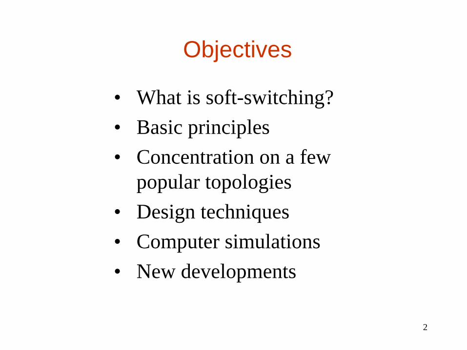
Objectives
• What is soft-switching?• Basic principles• Concentration on a few
popular topologies• Design techniques• Computer simulations• New developments

4
What is Soft-Switching
• Switching transitions occur under favorable conditions – device voltage or current is zero
• Reduced switching losses, switch stress, possibly low EMI, easier thermal management
• A must for very high frequency operation, (also medium frequency at high power levels)
• Usually involves compromises in conduction loss, switch rating, passive components etc.

5
Relationship Between Efficiency and Power Density
0.8 0.82 0.84 0.86 0.88 0.9 0.92 0.94 0.96
0
50
100
150
200
250
300
350
400
450
500
Pow
er R
atin
g
20lossP W=
10lossP W=
Efficiency0 8. 0 84. 0 88. 0 92. 0 96.
100
200
300
400
500
0
1
out
out loss
out loss
PP P
P P
η
ηη
=+
∴ =−

6
Hard-SwitchingiLiL +
-
+
-Vd
vT
vdiodei IL o≈
iT +
-
+
-Vd
vT
vdiodei IL o≈
iT
+
−gatev
Tv
Ti
lossP
diodei
diodev
( ) ( )on offsw s c cP f t t⎡ ⎤⎣ ⎦∝ +
7
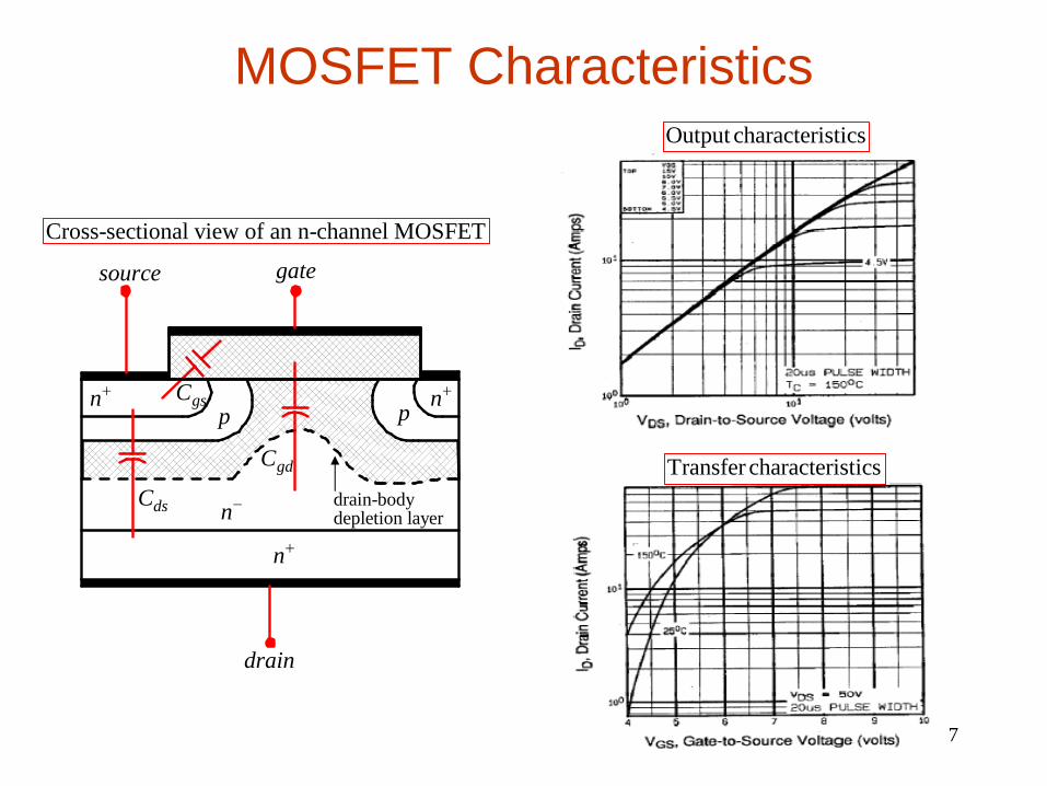
n+p
n−dsCgdC
drain-bodydepletion layer
gsCp n+
gatesource
drain
n+
Cross-sectional view of an n-channel MOSFET
MOSFET CharacteristicsOutput characteristics
Transfer characteristics

8
MOSFET Characteristics
inV
GGV
GRgdC
gsC
fDoI
( )D gsi f V=
MOSFET model valid inactive and cutoff regions
Variation of capacitances with dsV

9 Time
0s 0.5us 1.0us 1.5us 2.0us 2.5us 3.0us 3.5us 4.0usV(M1:d)/4 ID(M1)*2 V(R2:2) V(V3:+)
-10
0
10
200
V150V
80
D2I3
1A
R2
25.0
M1
IRF150
R31m
L2
40nH
Simulation of Hard Switching Converters
DSv
gateinput
DiGSv
Ideal diode
IRF150

10
Simulation of Hard Switching Converters
• Diode reverse recovery
Time
30.9500us 31.0000us 31.0500us 31.1000us30.9154us 31.1299us-I(R3) V(M1:1)/3 V(M1:2) I(I1)
0
20.0
38.5
Time
32.95us 33.00us 33.05us 33.10us 33.15us 33.20us 33.25us 33.30us33.34us-I(R3) V(M1:1)/3 V(M1:2) I(I1)
0
20.0
38.5
V1100
R2
10
M1
MTB
20N
20E
V4
TD = 1u
TF = 1nPW = 2uPER = {1/fs}
V1 = 0
TR = 1n
V2 = 15
PARAMETERS:
fs = 100kR_LOAD = 1
I15A
MU
R20
20R
D5
MTB20N20E
MUR2020R
Time
30.0us 30.4us 30.8us 31.2us 31.6us 32.0us 32.4us 32.8us 33.2us 33.6us 34.0us-I(R3) V(M1:1)/2 V(M1:2) I(I1)
0
20
40
-10
55
dsv
gsv
dsioI
dsv
oIgsvdsi
dsv
dsi oI
gsv

11
Problems of Hard-Switching
Possible Solutions (combination)• Snubbers to reduce di/dt and dv/dt
• Circuit layout to reduce stray inductances• Gate drive
• Soft switching to achieve ZVS and/or ZCS
usually no change in losses (unless loss recovery)
circuit layoutturn on / off speeds
• Switching losses • Device stress, thermal management• EMI due to high di/dt and dv/dt• Energy loss in stray L and C

12
Snubbers• Passive components (R, L, C) and a diode to shape
switching trajectories
Turn-on snubber (seldom used)
i t VL
tTd
s( )=
• low di/dt• lower turn-on losses in the device• low reverse recovery current
At turn-on
Price to be paid at turn-off• 1/2 LI2 energy dissipated during off interval• off interval > 2 to 3 times LS /RS time constant• switch voltage rating increases by RS IO
iT
Ls Rs
Io
+-
vT
t
Vd
vT
iTt0
0
iT
Ls Rs
Io
+-
vT
t
Vd
vT
iTt0
0

13
Turn-off Snubbers
At turn-off• while builds up
• switch turn-off loss decreases• lower dv/dt
i I iT o CS
i DC SS
= −( flows through )
Issues at turn-on• 1/2 CV2 energy dissipated in RS and switch• switch current rating increases by• ON interval > 2 to 3 times RS CS time constant
vT
Vd /R S
iT
Io
+
-vT CS
RS
Vd
DSiCS
iT
Io
+
-vT CS
RS
Vd
DSiCS
vT
iTIo
Vd0
CS1
CS2CS3
0C C CS S S3 2 1
> >
CS =0
vT
iTIo
Vd0
CS1
CS2CS3
0C C CS S S3 2 1
> >
CS =0

14
Soft-Switching
• ZVS (Zero Voltage Switching)• ZCS (Zero Current Switching)
Advantages - Lower losses (may be !) - Low EMI (may be !) - Allows high frequency operation

15
ZVS (Zero Voltage Switching)
Turn OFFTurn ON
• Switch voltage brought to zero before gate voltage is applied
• Ideal, zero-loss transition
• Low-loss transition• Parallel capacitor as a
loss-less snubber
• Preferred scheme for very high frequency applications using MOSFETs

16
ZCS (Zero Current Switching)
Best suited for converters with IGBTs due to tail current at turn-off
• Switch current brought to zero before gate voltage is removed
• Ideal, zero-loss transition
Turn OFF
Turn ON• Low-loss transition• Series inductor as a loss-less snubber• Energy in junction capacitance is lost

17
ZVS and Hard-Switched Waveforms
Zero-voltage switched Hard-switched
gate sourcev −
drain sourcev −
12V−
12V
gate sourcev −
drain sourcev −
0V 0V
12V−

18
An Example: Zero Voltage Transition (ZVT)
At t =0 is turned off, T +
( )( )
0 0
0-
C
dC
v
v V+ =
=
- dC Cv v V+ + =
dV
+
+
−
−oV
T+
T−
D+
D−
L
Li
C+
-C
Ci +
-Ci
A
Synchronous Buck Converter
Li
0

19
- dC CSince v v V+ + =
0-C C
s s
dv dvC C
dt dt++ =
0-C Ci i+∴ + =
0
-
C
dC
v
v V+∴ =
=0
dV
- LC CAlso, i - i i+ =
2-L
C C
ii -i+∴ = =
• At the end of this charge/discharge interval, positive iL is carried by
• Subsequently, is turned on; iL must reverse direction
D−
T−
dV
+
+
−
−oV
T+
T−
D+
D−
L
Li
sC+
-sC
Ci +
-Ci
A
Zero Voltage Transition (ZVT)

20
Zero Voltage Transition
dV
+
+
−
−oV
T+
T−
D+
D−
L
Li
sC+
-sC
Ci +
-Ci
A
ConductingDevices
0t 0’t 0
"t 1t 1’t 2t 3t
dVoV
Li
T+ T−D−
None NoneD+ T+
None
t
t
( )av t
0
0
( )Av t

21 Time
9us 10us 11us 12us 13us 14us 15us 16us 17usV(M2:d)/2 ID(M2)*2 V(M2:g) I(L1)*2 V(V8:+)
-20
-10
0
10
20
0
L1
20uHIC = 2A
V121V
C21000uFIC = 10V
M1
IRF150
M2
IRF150V8
TD = {TDLY2}
V7
TD = {TDLY1}
R7
25
R8
25
PARAMETERS:
PulseWidth = 4.5us
Period = 10us
TDLY1 = 5.5us
TDLY2 = 0.5us
R6
10.0
Simulation of a ZVT Buck Converter
DSv gateinput
Di
GSvLi
ZVT_buck.opj
22
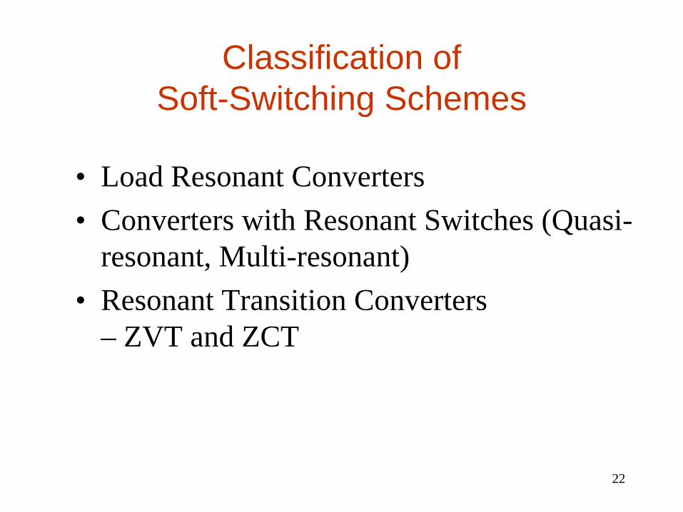
Classification of Soft-Switching Schemes
• Load Resonant Converters• Converters with Resonant Switches (Quasi-
resonant, Multi-resonant)• Resonant Transition Converters
– ZVT and ZCT

47
Makes use of switch capacitances and transformer leakage inductance and magnetizing current
Phase Shift Controlled Full-Bridge Converter (ZVT)
TA+
TA− TB
−
TB+
Db+
Db−Da
−
Da+
+−dV oIA
Ba
b
• Poles A & B switched at nearly 50% duty-cycle• Output voltage regulation is achieved by phase
modulating the two pole outputs
48
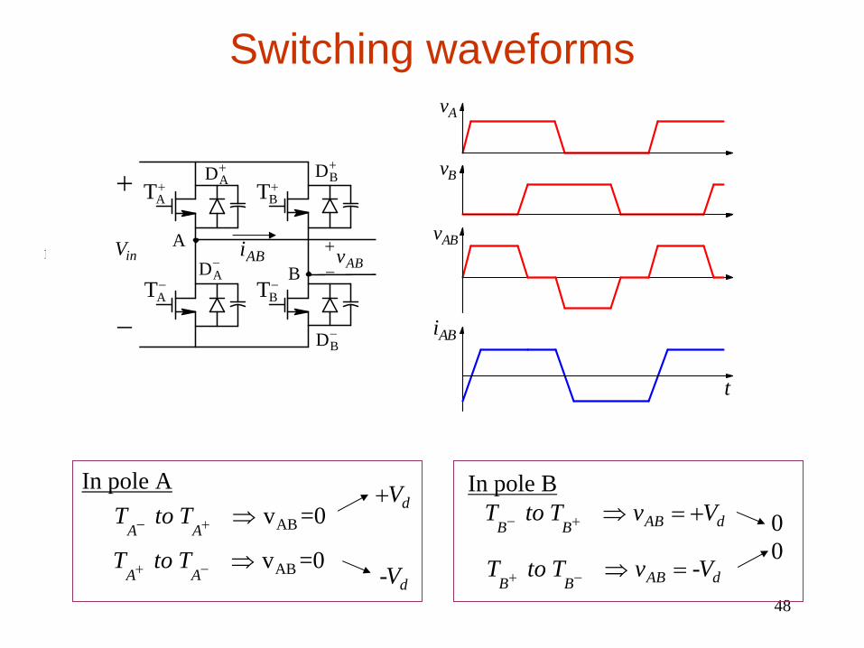
TA+
TA− TB
−
TB+
Db+
Db−Da
−
Da++
−2dV
oIA
B
a
b+−2
dV
DA+
DA−
DB−
DB+
lTL
0ficticious Li
+
−
inV ABi +− ABv
Switching waveforms
In pole A
ABv =0A A
T to T− + ⇒dV+
ABv =0A A
T to T+ − ⇒d-V
In pole BAB dB B
T to T v V− + ⇒ = +
AB dB BT to T v -V+ − ⇒ =
00
ABv
Bv
Av
ABi
t

49
Transitions - Pole B
T to TB B− +
0AB dv V= +
L oi stays at I
•
•
0AB dv -V=•
• L oi stays at - I
TA+
TB−
TB+
Db−
Da+
+−
IoA
Ba
bdV
Li
ABv
ABi
- +B BT to T
+ -B BT to T
t

50
Transitions - Pole A
0ABA AT to T v+ − ⇒ =
d-V
• All four diodes conduct• Leakage inductance resonates with switch capacitance• Determination of Tdel critical for ZVS design• Load dependent ZVS
Db−
Da+
LiTB
+
+−
oI
AB
abdV
TA−
TA+
ABvABi
+ -A AT to T
t

51
Methods to increase ZVS range• Use of external series inductor
DisadvantagesLoss of volt-sec
higher turns-ratio
higher conduction loss increased
VA ratings
Load dependent ZVS
+
−
Vin
+
−
VoA B
iAB
Lo
Lseries
+
−
vrect
iAB
vAB
0
left-leg
vrect
52
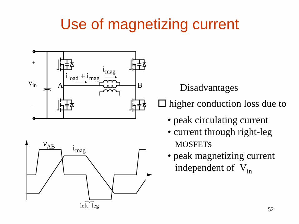
Use of magnetizing current
Disadvantageshigher conduction loss due to
• peak circulating current• current through right-leg
MOSFETs• peak magnetizing current
independent of Vin
i iload mag+imag
A B
+
−
Vin
imagvAB
left leg−2

53
Design of other parameters like Lo, Co, transformer etcidentical to hard switched PWM
Factors Affecting ZVS
Capacitance across MOSFETs– internal and external
Leakage inductanceDelay timeMagnetizing current
ZVS Load Range

54
Designing for ZVS
( ) ( )2
eqds in mag _ pk refl
ds
Lv V I I sin t
Cω= − +
12 eq dsL C
ωπ
=
( )12
eqmag _ pk refl in,max
ds
L. I I V
C+ ≥
2 22delay eq ds. T L . Cπ
=
Conditions for ZVS
MOSFET voltage during critical turn-on transition
dsv
t2
2 Lk dsL Cπ

55
A Possible Design Approach Using MathCAD
• Sweep for all practical values of
•
•
• Calculate total losses. Iterate for different ZVS ranges
dsC - based on limiting voltage rise during turn-offdelayT - as a percentage of switching period
mag,pk lkCalculate required I and L for each set
Calculate switch peak current and RMS current
Turn-off loss Conduction loss
Designing for ZVS
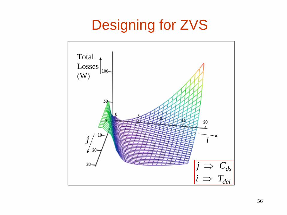
56
Designing for ZVS
Total_loss
Total Losses(W)
deli T⇒dsj C⇒
ij


![KEY-[1991]Novel Soft Switching PWM Converter Using a New Parallel Resonant DC-Link](https://static.fdocuments.in/doc/165x107/55cf96d2550346d0338e00ce/key-1991novel-soft-switching-pwm-converter-using-a-new-parallel-resonant.jpg)